KR101495580B1 - Leadframe, wiring board, light emitting unit, and illuminating apparatus - Google Patents
Leadframe, wiring board, light emitting unit, and illuminating apparatusDownload PDFInfo
- Publication number
- KR101495580B1 KR101495580B1KR1020127026385AKR20127026385AKR101495580B1KR 101495580 B1KR101495580 B1KR 101495580B1KR 1020127026385 AKR1020127026385 AKR 1020127026385AKR 20127026385 AKR20127026385 AKR 20127026385AKR 101495580 B1KR101495580 B1KR 101495580B1
- Authority
- KR
- South Korea
- Prior art keywords
- light emitting
- unit
- light
- led chip
- heat transfer
- Prior art date
- Legal status (The legal status is an assumption and is not a legal conclusion. Google has not performed a legal analysis and makes no representation as to the accuracy of the status listed.)
- Expired - Fee Related
Links
Images


Classifications
- H—ELECTRICITY
- H10—SEMICONDUCTOR DEVICES; ELECTRIC SOLID-STATE DEVICES NOT OTHERWISE PROVIDED FOR
- H10H—INORGANIC LIGHT-EMITTING SEMICONDUCTOR DEVICES HAVING POTENTIAL BARRIERS
- H10H20/00—Individual inorganic light-emitting semiconductor devices having potential barriers, e.g. light-emitting diodes [LED]
- H10H20/80—Constructional details
- H10H20/85—Packages
- H10H20/858—Means for heat extraction or cooling
- H—ELECTRICITY
- H05—ELECTRIC TECHNIQUES NOT OTHERWISE PROVIDED FOR
- H05K—PRINTED CIRCUITS; CASINGS OR CONSTRUCTIONAL DETAILS OF ELECTRIC APPARATUS; MANUFACTURE OF ASSEMBLAGES OF ELECTRICAL COMPONENTS
- H05K1/00—Printed circuits
- H05K1/02—Details
- H05K1/0201—Thermal arrangements, e.g. for cooling, heating or preventing overheating
- H05K1/0203—Cooling of mounted components
- F—MECHANICAL ENGINEERING; LIGHTING; HEATING; WEAPONS; BLASTING
- F21—LIGHTING
- F21K—NON-ELECTRIC LIGHT SOURCES USING LUMINESCENCE; LIGHT SOURCES USING ELECTROCHEMILUMINESCENCE; LIGHT SOURCES USING CHARGES OF COMBUSTIBLE MATERIAL; LIGHT SOURCES USING SEMICONDUCTOR DEVICES AS LIGHT-GENERATING ELEMENTS; LIGHT SOURCES NOT OTHERWISE PROVIDED FOR
- F21K9/00—Light sources using semiconductor devices as light-generating elements, e.g. using light-emitting diodes [LED] or lasers
- F21K9/20—Light sources comprising attachment means
- F21K9/27—Retrofit light sources for lighting devices with two fittings for each light source, e.g. for substitution of fluorescent tubes
- F—MECHANICAL ENGINEERING; LIGHTING; HEATING; WEAPONS; BLASTING
- F21—LIGHTING
- F21K—NON-ELECTRIC LIGHT SOURCES USING LUMINESCENCE; LIGHT SOURCES USING ELECTROCHEMILUMINESCENCE; LIGHT SOURCES USING CHARGES OF COMBUSTIBLE MATERIAL; LIGHT SOURCES USING SEMICONDUCTOR DEVICES AS LIGHT-GENERATING ELEMENTS; LIGHT SOURCES NOT OTHERWISE PROVIDED FOR
- F21K9/00—Light sources using semiconductor devices as light-generating elements, e.g. using light-emitting diodes [LED] or lasers
- F21K9/90—Methods of manufacture
- F—MECHANICAL ENGINEERING; LIGHTING; HEATING; WEAPONS; BLASTING
- F21—LIGHTING
- F21V—FUNCTIONAL FEATURES OR DETAILS OF LIGHTING DEVICES OR SYSTEMS THEREOF; STRUCTURAL COMBINATIONS OF LIGHTING DEVICES WITH OTHER ARTICLES, NOT OTHERWISE PROVIDED FOR
- F21V19/00—Fastening of light sources or lamp holders
- F21V19/001—Fastening of light sources or lamp holders the light sources being semiconductors devices, e.g. LEDs
- F21V19/003—Fastening of light source holders, e.g. of circuit boards or substrates holding light sources
- F21V19/004—Fastening of light source holders, e.g. of circuit boards or substrates holding light sources by deformation of parts or snap action mountings, e.g. using clips
- H—ELECTRICITY
- H01—ELECTRIC ELEMENTS
- H01L—SEMICONDUCTOR DEVICES NOT COVERED BY CLASS H10
- H01L24/00—Arrangements for connecting or disconnecting semiconductor or solid-state bodies; Methods or apparatus related thereto
- H01L24/93—Batch processes
- H01L24/95—Batch processes at chip-level, i.e. with connecting carried out on a plurality of singulated devices, i.e. on diced chips
- H01L24/97—Batch processes at chip-level, i.e. with connecting carried out on a plurality of singulated devices, i.e. on diced chips the devices being connected to a common substrate, e.g. interposer, said common substrate being separable into individual assemblies after connecting
- H—ELECTRICITY
- H05—ELECTRIC TECHNIQUES NOT OTHERWISE PROVIDED FOR
- H05K—PRINTED CIRCUITS; CASINGS OR CONSTRUCTIONAL DETAILS OF ELECTRIC APPARATUS; MANUFACTURE OF ASSEMBLAGES OF ELECTRICAL COMPONENTS
- H05K1/00—Printed circuits
- H05K1/18—Printed circuits structurally associated with non-printed electric components
- H05K1/181—Printed circuits structurally associated with non-printed electric components associated with surface mounted components
- F—MECHANICAL ENGINEERING; LIGHTING; HEATING; WEAPONS; BLASTING
- F21—LIGHTING
- F21K—NON-ELECTRIC LIGHT SOURCES USING LUMINESCENCE; LIGHT SOURCES USING ELECTROCHEMILUMINESCENCE; LIGHT SOURCES USING CHARGES OF COMBUSTIBLE MATERIAL; LIGHT SOURCES USING SEMICONDUCTOR DEVICES AS LIGHT-GENERATING ELEMENTS; LIGHT SOURCES NOT OTHERWISE PROVIDED FOR
- F21K9/00—Light sources using semiconductor devices as light-generating elements, e.g. using light-emitting diodes [LED] or lasers
- F21K9/20—Light sources comprising attachment means
- F—MECHANICAL ENGINEERING; LIGHTING; HEATING; WEAPONS; BLASTING
- F21—LIGHTING
- F21V—FUNCTIONAL FEATURES OR DETAILS OF LIGHTING DEVICES OR SYSTEMS THEREOF; STRUCTURAL COMBINATIONS OF LIGHTING DEVICES WITH OTHER ARTICLES, NOT OTHERWISE PROVIDED FOR
- F21V29/00—Protecting lighting devices from thermal damage; Cooling or heating arrangements specially adapted for lighting devices or systems
- F21V29/50—Cooling arrangements
- F21V29/70—Cooling arrangements characterised by passive heat-dissipating elements, e.g. heat-sinks
- F21V29/74—Cooling arrangements characterised by passive heat-dissipating elements, e.g. heat-sinks with fins or blades
- F21V29/76—Cooling arrangements characterised by passive heat-dissipating elements, e.g. heat-sinks with fins or blades with essentially identical parallel planar fins or blades, e.g. with comb-like cross-section
- F21V29/767—Cooling arrangements characterised by passive heat-dissipating elements, e.g. heat-sinks with fins or blades with essentially identical parallel planar fins or blades, e.g. with comb-like cross-section the planes containing the fins or blades having directions perpendicular to the light emitting axis
- F—MECHANICAL ENGINEERING; LIGHTING; HEATING; WEAPONS; BLASTING
- F21—LIGHTING
- F21Y—INDEXING SCHEME ASSOCIATED WITH SUBCLASSES F21K, F21L, F21S and F21V, RELATING TO THE FORM OR THE KIND OF THE LIGHT SOURCES OR OF THE COLOUR OF THE LIGHT EMITTED
- F21Y2103/00—Elongate light sources, e.g. fluorescent tubes
- F21Y2103/10—Elongate light sources, e.g. fluorescent tubes comprising a linear array of point-like light-generating elements
- F—MECHANICAL ENGINEERING; LIGHTING; HEATING; WEAPONS; BLASTING
- F21—LIGHTING
- F21Y—INDEXING SCHEME ASSOCIATED WITH SUBCLASSES F21K, F21L, F21S and F21V, RELATING TO THE FORM OR THE KIND OF THE LIGHT SOURCES OR OF THE COLOUR OF THE LIGHT EMITTED
- F21Y2105/00—Planar light sources
- F21Y2105/10—Planar light sources comprising a two-dimensional array of point-like light-generating elements
- F—MECHANICAL ENGINEERING; LIGHTING; HEATING; WEAPONS; BLASTING
- F21—LIGHTING
- F21Y—INDEXING SCHEME ASSOCIATED WITH SUBCLASSES F21K, F21L, F21S and F21V, RELATING TO THE FORM OR THE KIND OF THE LIGHT SOURCES OR OF THE COLOUR OF THE LIGHT EMITTED
- F21Y2107/00—Light sources with three-dimensionally disposed light-generating elements
- F21Y2107/90—Light sources with three-dimensionally disposed light-generating elements on two opposite sides of supports or substrates
- F—MECHANICAL ENGINEERING; LIGHTING; HEATING; WEAPONS; BLASTING
- F21—LIGHTING
- F21Y—INDEXING SCHEME ASSOCIATED WITH SUBCLASSES F21K, F21L, F21S and F21V, RELATING TO THE FORM OR THE KIND OF THE LIGHT SOURCES OR OF THE COLOUR OF THE LIGHT EMITTED
- F21Y2115/00—Light-generating elements of semiconductor light sources
- F21Y2115/10—Light-emitting diodes [LED]
- H—ELECTRICITY
- H01—ELECTRIC ELEMENTS
- H01L—SEMICONDUCTOR DEVICES NOT COVERED BY CLASS H10
- H01L2224/00—Indexing scheme for arrangements for connecting or disconnecting semiconductor or solid-state bodies and methods related thereto as covered by H01L24/00
- H01L2224/01—Means for bonding being attached to, or being formed on, the surface to be connected, e.g. chip-to-package, die-attach, "first-level" interconnects; Manufacturing methods related thereto
- H01L2224/42—Wire connectors; Manufacturing methods related thereto
- H01L2224/44—Structure, shape, material or disposition of the wire connectors prior to the connecting process
- H01L2224/45—Structure, shape, material or disposition of the wire connectors prior to the connecting process of an individual wire connector
- H01L2224/45001—Core members of the connector
- H01L2224/45099—Material
- H01L2224/451—Material with a principal constituent of the material being a metal or a metalloid, e.g. boron (B), silicon (Si), germanium (Ge), arsenic (As), antimony (Sb), tellurium (Te) and polonium (Po), and alloys thereof
- H01L2224/45117—Material with a principal constituent of the material being a metal or a metalloid, e.g. boron (B), silicon (Si), germanium (Ge), arsenic (As), antimony (Sb), tellurium (Te) and polonium (Po), and alloys thereof the principal constituent melting at a temperature of greater than or equal to 400°C and less than 950°C
- H01L2224/45124—Aluminium (Al) as principal constituent
- H—ELECTRICITY
- H01—ELECTRIC ELEMENTS
- H01L—SEMICONDUCTOR DEVICES NOT COVERED BY CLASS H10
- H01L2224/00—Indexing scheme for arrangements for connecting or disconnecting semiconductor or solid-state bodies and methods related thereto as covered by H01L24/00
- H01L2224/01—Means for bonding being attached to, or being formed on, the surface to be connected, e.g. chip-to-package, die-attach, "first-level" interconnects; Manufacturing methods related thereto
- H01L2224/42—Wire connectors; Manufacturing methods related thereto
- H01L2224/44—Structure, shape, material or disposition of the wire connectors prior to the connecting process
- H01L2224/45—Structure, shape, material or disposition of the wire connectors prior to the connecting process of an individual wire connector
- H01L2224/45001—Core members of the connector
- H01L2224/45099—Material
- H01L2224/451—Material with a principal constituent of the material being a metal or a metalloid, e.g. boron (B), silicon (Si), germanium (Ge), arsenic (As), antimony (Sb), tellurium (Te) and polonium (Po), and alloys thereof
- H01L2224/45138—Material with a principal constituent of the material being a metal or a metalloid, e.g. boron (B), silicon (Si), germanium (Ge), arsenic (As), antimony (Sb), tellurium (Te) and polonium (Po), and alloys thereof the principal constituent melting at a temperature of greater than or equal to 950°C and less than 1550°C
- H01L2224/45139—Silver (Ag) as principal constituent
- H—ELECTRICITY
- H01—ELECTRIC ELEMENTS
- H01L—SEMICONDUCTOR DEVICES NOT COVERED BY CLASS H10
- H01L2224/00—Indexing scheme for arrangements for connecting or disconnecting semiconductor or solid-state bodies and methods related thereto as covered by H01L24/00
- H01L2224/01—Means for bonding being attached to, or being formed on, the surface to be connected, e.g. chip-to-package, die-attach, "first-level" interconnects; Manufacturing methods related thereto
- H01L2224/42—Wire connectors; Manufacturing methods related thereto
- H01L2224/44—Structure, shape, material or disposition of the wire connectors prior to the connecting process
- H01L2224/45—Structure, shape, material or disposition of the wire connectors prior to the connecting process of an individual wire connector
- H01L2224/45001—Core members of the connector
- H01L2224/45099—Material
- H01L2224/451—Material with a principal constituent of the material being a metal or a metalloid, e.g. boron (B), silicon (Si), germanium (Ge), arsenic (As), antimony (Sb), tellurium (Te) and polonium (Po), and alloys thereof
- H01L2224/45138—Material with a principal constituent of the material being a metal or a metalloid, e.g. boron (B), silicon (Si), germanium (Ge), arsenic (As), antimony (Sb), tellurium (Te) and polonium (Po), and alloys thereof the principal constituent melting at a temperature of greater than or equal to 950°C and less than 1550°C
- H01L2224/45144—Gold (Au) as principal constituent
- H—ELECTRICITY
- H01—ELECTRIC ELEMENTS
- H01L—SEMICONDUCTOR DEVICES NOT COVERED BY CLASS H10
- H01L2224/00—Indexing scheme for arrangements for connecting or disconnecting semiconductor or solid-state bodies and methods related thereto as covered by H01L24/00
- H01L2224/01—Means for bonding being attached to, or being formed on, the surface to be connected, e.g. chip-to-package, die-attach, "first-level" interconnects; Manufacturing methods related thereto
- H01L2224/42—Wire connectors; Manufacturing methods related thereto
- H01L2224/47—Structure, shape, material or disposition of the wire connectors after the connecting process
- H01L2224/48—Structure, shape, material or disposition of the wire connectors after the connecting process of an individual wire connector
- H01L2224/4805—Shape
- H01L2224/4809—Loop shape
- H01L2224/48091—Arched
- H—ELECTRICITY
- H01—ELECTRIC ELEMENTS
- H01L—SEMICONDUCTOR DEVICES NOT COVERED BY CLASS H10
- H01L2224/00—Indexing scheme for arrangements for connecting or disconnecting semiconductor or solid-state bodies and methods related thereto as covered by H01L24/00
- H01L2224/01—Means for bonding being attached to, or being formed on, the surface to be connected, e.g. chip-to-package, die-attach, "first-level" interconnects; Manufacturing methods related thereto
- H01L2224/42—Wire connectors; Manufacturing methods related thereto
- H01L2224/47—Structure, shape, material or disposition of the wire connectors after the connecting process
- H01L2224/48—Structure, shape, material or disposition of the wire connectors after the connecting process of an individual wire connector
- H01L2224/481—Disposition
- H01L2224/48135—Connecting between different semiconductor or solid-state bodies, i.e. chip-to-chip
- H01L2224/48137—Connecting between different semiconductor or solid-state bodies, i.e. chip-to-chip the bodies being arranged next to each other, e.g. on a common substrate
- H—ELECTRICITY
- H01—ELECTRIC ELEMENTS
- H01L—SEMICONDUCTOR DEVICES NOT COVERED BY CLASS H10
- H01L2224/00—Indexing scheme for arrangements for connecting or disconnecting semiconductor or solid-state bodies and methods related thereto as covered by H01L24/00
- H01L2224/01—Means for bonding being attached to, or being formed on, the surface to be connected, e.g. chip-to-package, die-attach, "first-level" interconnects; Manufacturing methods related thereto
- H01L2224/42—Wire connectors; Manufacturing methods related thereto
- H01L2224/47—Structure, shape, material or disposition of the wire connectors after the connecting process
- H01L2224/48—Structure, shape, material or disposition of the wire connectors after the connecting process of an individual wire connector
- H01L2224/481—Disposition
- H01L2224/48151—Connecting between a semiconductor or solid-state body and an item not being a semiconductor or solid-state body, e.g. chip-to-substrate, chip-to-passive
- H01L2224/48221—Connecting between a semiconductor or solid-state body and an item not being a semiconductor or solid-state body, e.g. chip-to-substrate, chip-to-passive the body and the item being stacked
- H01L2224/48225—Connecting between a semiconductor or solid-state body and an item not being a semiconductor or solid-state body, e.g. chip-to-substrate, chip-to-passive the body and the item being stacked the item being non-metallic, e.g. insulating substrate with or without metallisation
- H01L2224/48227—Connecting between a semiconductor or solid-state body and an item not being a semiconductor or solid-state body, e.g. chip-to-substrate, chip-to-passive the body and the item being stacked the item being non-metallic, e.g. insulating substrate with or without metallisation connecting the wire to a bond pad of the item
- H01L2224/48228—Connecting between a semiconductor or solid-state body and an item not being a semiconductor or solid-state body, e.g. chip-to-substrate, chip-to-passive the body and the item being stacked the item being non-metallic, e.g. insulating substrate with or without metallisation connecting the wire to a bond pad of the item the bond pad being disposed in a recess of the surface of the item
- H—ELECTRICITY
- H01—ELECTRIC ELEMENTS
- H01L—SEMICONDUCTOR DEVICES NOT COVERED BY CLASS H10
- H01L2224/00—Indexing scheme for arrangements for connecting or disconnecting semiconductor or solid-state bodies and methods related thereto as covered by H01L24/00
- H01L2224/01—Means for bonding being attached to, or being formed on, the surface to be connected, e.g. chip-to-package, die-attach, "first-level" interconnects; Manufacturing methods related thereto
- H01L2224/42—Wire connectors; Manufacturing methods related thereto
- H01L2224/47—Structure, shape, material or disposition of the wire connectors after the connecting process
- H01L2224/49—Structure, shape, material or disposition of the wire connectors after the connecting process of a plurality of wire connectors
- H01L2224/491—Disposition
- H01L2224/4911—Disposition the connectors being bonded to at least one common bonding area, e.g. daisy chain
- H01L2224/49113—Disposition the connectors being bonded to at least one common bonding area, e.g. daisy chain the connectors connecting different bonding areas on the semiconductor or solid-state body to a common bonding area outside the body, e.g. converging wires
- H—ELECTRICITY
- H01—ELECTRIC ELEMENTS
- H01L—SEMICONDUCTOR DEVICES NOT COVERED BY CLASS H10
- H01L2224/00—Indexing scheme for arrangements for connecting or disconnecting semiconductor or solid-state bodies and methods related thereto as covered by H01L24/00
- H01L2224/01—Means for bonding being attached to, or being formed on, the surface to be connected, e.g. chip-to-package, die-attach, "first-level" interconnects; Manufacturing methods related thereto
- H01L2224/42—Wire connectors; Manufacturing methods related thereto
- H01L2224/47—Structure, shape, material or disposition of the wire connectors after the connecting process
- H01L2224/49—Structure, shape, material or disposition of the wire connectors after the connecting process of a plurality of wire connectors
- H01L2224/491—Disposition
- H01L2224/4912—Layout
- H01L2224/49171—Fan-out arrangements
- H—ELECTRICITY
- H01—ELECTRIC ELEMENTS
- H01L—SEMICONDUCTOR DEVICES NOT COVERED BY CLASS H10
- H01L2224/00—Indexing scheme for arrangements for connecting or disconnecting semiconductor or solid-state bodies and methods related thereto as covered by H01L24/00
- H01L2224/73—Means for bonding being of different types provided for in two or more of groups H01L2224/10, H01L2224/18, H01L2224/26, H01L2224/34, H01L2224/42, H01L2224/50, H01L2224/63, H01L2224/71
- H01L2224/732—Location after the connecting process
- H01L2224/73251—Location after the connecting process on different surfaces
- H01L2224/73265—Layer and wire connectors
- H—ELECTRICITY
- H01—ELECTRIC ELEMENTS
- H01L—SEMICONDUCTOR DEVICES NOT COVERED BY CLASS H10
- H01L24/00—Arrangements for connecting or disconnecting semiconductor or solid-state bodies; Methods or apparatus related thereto
- H01L24/01—Means for bonding being attached to, or being formed on, the surface to be connected, e.g. chip-to-package, die-attach, "first-level" interconnects; Manufacturing methods related thereto
- H01L24/42—Wire connectors; Manufacturing methods related thereto
- H01L24/44—Structure, shape, material or disposition of the wire connectors prior to the connecting process
- H01L24/45—Structure, shape, material or disposition of the wire connectors prior to the connecting process of an individual wire connector
- H—ELECTRICITY
- H01—ELECTRIC ELEMENTS
- H01L—SEMICONDUCTOR DEVICES NOT COVERED BY CLASS H10
- H01L25/00—Assemblies consisting of a plurality of semiconductor or other solid state devices
- H01L25/03—Assemblies consisting of a plurality of semiconductor or other solid state devices all the devices being of a type provided for in a single subclass of subclasses H10B, H10D, H10F, H10H, H10K or H10N, e.g. assemblies of rectifier diodes
- H01L25/04—Assemblies consisting of a plurality of semiconductor or other solid state devices all the devices being of a type provided for in a single subclass of subclasses H10B, H10D, H10F, H10H, H10K or H10N, e.g. assemblies of rectifier diodes the devices not having separate containers
- H01L25/075—Assemblies consisting of a plurality of semiconductor or other solid state devices all the devices being of a type provided for in a single subclass of subclasses H10B, H10D, H10F, H10H, H10K or H10N, e.g. assemblies of rectifier diodes the devices not having separate containers the devices being of a type provided for in group H10H20/00
- H01L25/0753—Assemblies consisting of a plurality of semiconductor or other solid state devices all the devices being of a type provided for in a single subclass of subclasses H10B, H10D, H10F, H10H, H10K or H10N, e.g. assemblies of rectifier diodes the devices not having separate containers the devices being of a type provided for in group H10H20/00 the devices being arranged next to each other
- H—ELECTRICITY
- H01—ELECTRIC ELEMENTS
- H01L—SEMICONDUCTOR DEVICES NOT COVERED BY CLASS H10
- H01L2924/00—Indexing scheme for arrangements or methods for connecting or disconnecting semiconductor or solid-state bodies as covered by H01L24/00
- H01L2924/0001—Technical content checked by a classifier
- H01L2924/00011—Not relevant to the scope of the group, the symbol of which is combined with the symbol of this group
- H—ELECTRICITY
- H01—ELECTRIC ELEMENTS
- H01L—SEMICONDUCTOR DEVICES NOT COVERED BY CLASS H10
- H01L2924/00—Indexing scheme for arrangements or methods for connecting or disconnecting semiconductor or solid-state bodies as covered by H01L24/00
- H01L2924/0001—Technical content checked by a classifier
- H01L2924/00014—Technical content checked by a classifier the subject-matter covered by the group, the symbol of which is combined with the symbol of this group, being disclosed without further technical details
- H—ELECTRICITY
- H01—ELECTRIC ELEMENTS
- H01L—SEMICONDUCTOR DEVICES NOT COVERED BY CLASS H10
- H01L2924/00—Indexing scheme for arrangements or methods for connecting or disconnecting semiconductor or solid-state bodies as covered by H01L24/00
- H01L2924/10—Details of semiconductor or other solid state devices to be connected
- H01L2924/11—Device type
- H01L2924/12—Passive devices, e.g. 2 terminal devices
- H01L2924/1203—Rectifying Diode
- H01L2924/12035—Zener diode
- H—ELECTRICITY
- H01—ELECTRIC ELEMENTS
- H01L—SEMICONDUCTOR DEVICES NOT COVERED BY CLASS H10
- H01L2924/00—Indexing scheme for arrangements or methods for connecting or disconnecting semiconductor or solid-state bodies as covered by H01L24/00
- H01L2924/10—Details of semiconductor or other solid state devices to be connected
- H01L2924/11—Device type
- H01L2924/12—Passive devices, e.g. 2 terminal devices
- H01L2924/1204—Optical Diode
- H01L2924/12041—LED
- H—ELECTRICITY
- H01—ELECTRIC ELEMENTS
- H01L—SEMICONDUCTOR DEVICES NOT COVERED BY CLASS H10
- H01L2924/00—Indexing scheme for arrangements or methods for connecting or disconnecting semiconductor or solid-state bodies as covered by H01L24/00
- H01L2924/10—Details of semiconductor or other solid state devices to be connected
- H01L2924/11—Device type
- H01L2924/12—Passive devices, e.g. 2 terminal devices
- H01L2924/1204—Optical Diode
- H01L2924/12042—LASER
- H—ELECTRICITY
- H01—ELECTRIC ELEMENTS
- H01L—SEMICONDUCTOR DEVICES NOT COVERED BY CLASS H10
- H01L2924/00—Indexing scheme for arrangements or methods for connecting or disconnecting semiconductor or solid-state bodies as covered by H01L24/00
- H01L2924/15—Details of package parts other than the semiconductor or other solid state devices to be connected
- H01L2924/181—Encapsulation
- H—ELECTRICITY
- H05—ELECTRIC TECHNIQUES NOT OTHERWISE PROVIDED FOR
- H05K—PRINTED CIRCUITS; CASINGS OR CONSTRUCTIONAL DETAILS OF ELECTRIC APPARATUS; MANUFACTURE OF ASSEMBLAGES OF ELECTRICAL COMPONENTS
- H05K1/00—Printed circuits
- H05K1/02—Details
- H05K1/0271—Arrangements for reducing stress or warp in rigid printed circuit boards, e.g. caused by loads, vibrations or differences in thermal expansion
- H—ELECTRICITY
- H05—ELECTRIC TECHNIQUES NOT OTHERWISE PROVIDED FOR
- H05K—PRINTED CIRCUITS; CASINGS OR CONSTRUCTIONAL DETAILS OF ELECTRIC APPARATUS; MANUFACTURE OF ASSEMBLAGES OF ELECTRICAL COMPONENTS
- H05K1/00—Printed circuits
- H05K1/02—Details
- H05K1/03—Use of materials for the substrate
- H05K1/05—Insulated conductive substrates, e.g. insulated metal substrate
- H05K1/056—Insulated conductive substrates, e.g. insulated metal substrate the metal substrate being covered by an organic insulating layer
- H—ELECTRICITY
- H05—ELECTRIC TECHNIQUES NOT OTHERWISE PROVIDED FOR
- H05K—PRINTED CIRCUITS; CASINGS OR CONSTRUCTIONAL DETAILS OF ELECTRIC APPARATUS; MANUFACTURE OF ASSEMBLAGES OF ELECTRICAL COMPONENTS
- H05K2201/00—Indexing scheme relating to printed circuits covered by H05K1/00
- H05K2201/10—Details of components or other objects attached to or integrated in a printed circuit board
- H05K2201/10007—Types of components
- H05K2201/10106—Light emitting diode [LED]
- H—ELECTRICITY
- H05—ELECTRIC TECHNIQUES NOT OTHERWISE PROVIDED FOR
- H05K—PRINTED CIRCUITS; CASINGS OR CONSTRUCTIONAL DETAILS OF ELECTRIC APPARATUS; MANUFACTURE OF ASSEMBLAGES OF ELECTRICAL COMPONENTS
- H05K3/00—Apparatus or processes for manufacturing printed circuits
- H05K3/10—Apparatus or processes for manufacturing printed circuits in which conductive material is applied to the insulating support in such a manner as to form the desired conductive pattern
- H05K3/20—Apparatus or processes for manufacturing printed circuits in which conductive material is applied to the insulating support in such a manner as to form the desired conductive pattern by affixing prefabricated conductor pattern
- H05K3/202—Apparatus or processes for manufacturing printed circuits in which conductive material is applied to the insulating support in such a manner as to form the desired conductive pattern by affixing prefabricated conductor pattern using self-supporting metal foil pattern
- H—ELECTRICITY
- H10—SEMICONDUCTOR DEVICES; ELECTRIC SOLID-STATE DEVICES NOT OTHERWISE PROVIDED FOR
- H10H—INORGANIC LIGHT-EMITTING SEMICONDUCTOR DEVICES HAVING POTENTIAL BARRIERS
- H10H20/00—Individual inorganic light-emitting semiconductor devices having potential barriers, e.g. light-emitting diodes [LED]
- H10H20/80—Constructional details
- H10H20/85—Packages
- H10H20/8506—Containers
- H—ELECTRICITY
- H10—SEMICONDUCTOR DEVICES; ELECTRIC SOLID-STATE DEVICES NOT OTHERWISE PROVIDED FOR
- H10H—INORGANIC LIGHT-EMITTING SEMICONDUCTOR DEVICES HAVING POTENTIAL BARRIERS
- H10H20/00—Individual inorganic light-emitting semiconductor devices having potential barriers, e.g. light-emitting diodes [LED]
- H10H20/80—Constructional details
- H10H20/85—Packages
- H10H20/857—Interconnections, e.g. lead-frames, bond wires or solder balls
- Y—GENERAL TAGGING OF NEW TECHNOLOGICAL DEVELOPMENTS; GENERAL TAGGING OF CROSS-SECTIONAL TECHNOLOGIES SPANNING OVER SEVERAL SECTIONS OF THE IPC; TECHNICAL SUBJECTS COVERED BY FORMER USPC CROSS-REFERENCE ART COLLECTIONS [XRACs] AND DIGESTS
- Y02—TECHNOLOGIES OR APPLICATIONS FOR MITIGATION OR ADAPTATION AGAINST CLIMATE CHANGE
- Y02P—CLIMATE CHANGE MITIGATION TECHNOLOGIES IN THE PRODUCTION OR PROCESSING OF GOODS
- Y02P70/00—Climate change mitigation technologies in the production process for final industrial or consumer products
- Y02P70/50—Manufacturing or production processes characterised by the final manufactured product
- Y—GENERAL TAGGING OF NEW TECHNOLOGICAL DEVELOPMENTS; GENERAL TAGGING OF CROSS-SECTIONAL TECHNOLOGIES SPANNING OVER SEVERAL SECTIONS OF THE IPC; TECHNICAL SUBJECTS COVERED BY FORMER USPC CROSS-REFERENCE ART COLLECTIONS [XRACs] AND DIGESTS
- Y10—TECHNICAL SUBJECTS COVERED BY FORMER USPC
- Y10S—TECHNICAL SUBJECTS COVERED BY FORMER USPC CROSS-REFERENCE ART COLLECTIONS [XRACs] AND DIGESTS
- Y10S362/00—Illumination
- Y10S362/80—Light emitting diode
Landscapes
- Engineering & Computer Science (AREA)
- Microelectronics & Electronic Packaging (AREA)
- General Engineering & Computer Science (AREA)
- Physics & Mathematics (AREA)
- Optics & Photonics (AREA)
- Manufacturing & Machinery (AREA)
- Computer Hardware Design (AREA)
- Power Engineering (AREA)
- Led Device Packages (AREA)
Abstract
Translated fromKorean
Description
Translated fromKorean본 발명은 리드 프레임, 배선판, 발광 유닛, 조명 장치에 관한 것이다.The present invention relates to a lead frame, a wiring board, a light emitting unit, and a lighting apparatus.
종래부터, LED 칩을 이용한 발광 장치의 제조에 사용되는 리드 프레임이 제안되어 있다(예를 들면, 일본 공개특허공보 제2006-93470호: 특허 문헌 1).Background Art [0002] A lead frame used for manufacturing a light emitting device using an LED chip has been proposed (for example, Japanese Patent Laid-Open Publication No. 2006-93470: Patent Document 1).
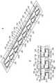
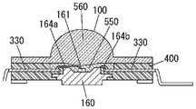
이 특허 문헌 1에는, 도 60에 나타낸 바와 같이, 히트 싱크(heat sink)(160), 이 히트 싱크(160)에 마운트된 LED 칩(161), LED 칩(161) 및 히트 싱크(160)에 각각 본딩 와이어(164a, 164b)를 통하여 전기적으로 접속된 한 쌍의 리드부(330), 히트 싱크(100) 및 각 리드부(330)를 일체적으로 유지하는 동시에 LED 칩(161)을 전면 측에서 노출시키는 수지 패키지(400), 및 이 수지 패키지(400)의 전면 측에 광투과성의 수지부(550)를 개재하여 덮도록 장착된 보조 렌즈(attachment lens)(560)를 구비한 발광 장치(100)가 기재되어 있다.60, a
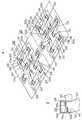
또, 특허 문헌 1에는, 도 60의 발광 장치(100)의 제조에 사용하는 리드 프레임(300)으로서 도 61에 나타낸 구성의 것이 기재되어 있다. 이 리드 프레임(300)은, 서로 평행하게 형성된 한 쌍의 장척(長尺)의 평행 프레임부(310), 평행 프레임부(310)의 길이 방향에 있어서 등간격으로 배치되고 대향하는 평행 프레임부(310)끼리를 연결하는 연결 프레임부(320), 서로 인접하는 연결 프레임부(320)의 중앙부에서 서로 근접하는 방향으로 연장되어 단부끼리가 서로 일정하게 정해진(소정) 거리를 두고 대치하도록 형성된 한 쌍의 리드부(330), 및 한 쌍의 평행 프레임부(310)로부터 각각의 리드부(330)의 단부를 향해 연장된 지지 프레임부(340)가 일체적으로 형성되어 있다.In addition,
또, 종래부터, 도 62의 A, 도 62의 B에 나타낸 바와 같이, 광원 장치(101)와, 광원 장치(101)에 동작 전원을 공급하는 전원 장치(102)와, 및 이들을 수납하는 기구 본체(103)를 구비한 조명 기구(L)가 제안되어 있다(일본 공개특허공보 제2007-35890호: 특허 문헌 2).As shown in Figs. 62A and 62B, a
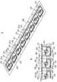
광원 장치(101)는, 광원 블록(BK)과, 광원 블록(BK)을 수납하는 케이스(106)를 구비하고 있다. 광원 블록(BK)은, 도 63에 나타낸 바와 같이, 배선 패턴(111)이 일면 측(표면 측)에 형성된 장척형의 인쇄 기판(110)과, 인쇄 기판(110)의 배선 패턴(111)에 리플로우 납땜(reflow soldering)에 의해 면실장되는 복수의 발광 다이오드(4A∼4L)를 구비하고 있다.The
발광 다이오드(4A∼4L)는, 이른바 면실장형의 고휘도 백색 발광 다이오드이고, 표면(表面)이 출사구(40)(도 64의 A 참조)를 구비한 출사면, 이면(裏面)이 애노드 단자(도시하지 않음) 및 캐소드 단자(도시하지 않음)가 노출된 실장면으로 되어 있다. 그리고, 특허 문헌 2에는, 발광 다이오드(4A∼4L)가, 도 64의 A에 나타낸 바와 같이, 인쇄 기판(110)의 길이 방향으로 대략 등간격으로 줄지어 설치되어, 의사적인 선(線) 광원으로서 사용되는 취지가 기재되어 있다.The
인쇄 기판(110)은, 도 63의 A, 도 63의 B에 나타낸 바와 같이, 장척 직사각형 판형으로 형성된 편면 실장 기판이며, 좌단 측에는, 배선 패턴(111)에 전원 장치(102)의 출력용 전원선(107a∼107c)(도 62의 A 참조)을 접속하기 위한 3개의 관통 구멍(110a)이 관통 설치되어 있다. 또, 이 인쇄 기판(110)의 길이 방향의 양단부 및 중앙부에는, 인쇄 기판(110)을 기구 본체(103)에 고정하기 위한 고정 나사(S1)(도 62 참조)가 장착되는 나사 구멍(110b)이 관통 설치되어 있다.The printed
인쇄 기판(110)의 재료로서는, 종이 기재(base material) 에폭시 수지 동장적층판 등의 종이 기재 동장적층판, 유리섬유(glass fabric) 기재 에폭시 수지 동장적층판 등의 유리 섬유 기재 동장적층판, 유리섬유 부직포(glass nonwoven fabric) 기재 에폭시 수지 동장적층판 등의 유리섬유 부직포 동장적층판이 기재되어 있다.Examples of the material of the printed
이 인쇄 기판(110)의 표면 측에는, 도 63의 A에 나타낸 바와 같이, 발광 다이오드(4A∼4L) 등이 접속되는 배선 패턴(111)이 형성되어 있다.A
이 배선 패턴(111)은 동박 등의 도전 재료를 사용하여 형성되어 있다. 이 인쇄 기판(110)에서는, 발광 다이오드(4A∼4F)의 직렬 회로와, 발광 다이오드(4G∼4L)의 직렬 회로가 순방향으로 병렬 접속된다.The
또, 인쇄 기판(110)의 표면 측에는, 배선 패턴(111)에서, 발광 다이오드(4A∼4L) 등과의 접속에 필요한 부분만을 노출시켜, 필요한 곳 외에 땜납이 부착되는 것을 방지하기 위한 솔더 레지스트(solder resist)(112)(도 64의 A 참조)가 형성되어 있다.On the surface side of the printed
한편, 인쇄 기판(110) 다른 면 측(이면 측)에는, 휨 방지부(113)가 형성되어 있다. 이 휨 방지부(113)는, 도 63의 B에 나타낸 바와 같이, 동박을 사용하여 배선 패턴(111)과 대략 같은 형상으로 형성되어 있다. 즉, 휨 방지부(113)는 배선 패턴(111)과 대략 같은 형상의 더미용 배선 패턴이다.On the other hand, on the other surface side (back side) of the printed
발광 다이오드(4A∼4L)는 인쇄 기판(110)에 면실장되어 있지만, 이것은 리플로우 납땜에 의해 행해지고 있다. 인쇄 기판(110)을 리플로우 노(爐)를 통과시켰을 때는, 인쇄 기판(110)의 열팽창 계수보다 배선 패턴(111)의 열팽창 계수가 작으므로, 이들 열팽창 계수의 차이에 의해, 인쇄 기판(110)의 표면 측의 열팽창이 억제되어, 인쇄 기판(110)에는 표면 측으로 휘게 하는 힘이 생기게 된다. 그러나, 전술한 인쇄 기판(110)은, 이면 측에 배선 패턴(111)과 대략 같은 형상의 휨 방지부(113)를 형성하고 있으므로, 휨 방지부(113)와 인쇄 기판(110)과의 열팽창 계수의 차이에 의해, 인쇄 기판(110)의 이면 측에서도 열팽창이 억제되고, 인쇄 기판(110)에는 이면 측으로 휘게 하는 힘이 생긴다. 그러므로, 인쇄 기판(110)에서는, 양면(표면 및 이면)에서 열팽창이 억제되고, 그 결과, 배선 패턴(111)과 인쇄 기판(110)의 열팽창 계수의 차에 기인하는 휨과, 휨 방지부(113)와 인쇄 기판(110)과의 열팽창 계수의 차에 기인하는 휨은 서로 상쇄되고, 인쇄 기판(110)의 휨은 감소된다. 그리고, 리플로우 노를 통과한 후에, 인쇄 기판(110)의 온도가 떨어졌을 때도 온도 변화에 의해 휘어지려고 하지만, 상기와 동일한 이유로 인쇄 기판(110)의 휨은 감소된다.The
광원 블록(BK)이 수납되는 케이스(106)는 아크릴 수지 등의 투광성을 가지는 합성 수지를 사용하여, 하면이 개구된 장척 상자형으로 형성되어 있고, 그 길이 방향의 양 내측면의 하단 에지부에는, 케이스(106) 내에 수납된 인쇄 기판(110)을 지지하기 위한 지지편(106a, 106a)이 일체로 돌출 설치되어 있다.The
광원 장치(101)의 케이스(106) 내에는, 케이스(106)를 전체적으로 빛나게 하기 위하여, 그리고 광원 블록(BK)의 방열성과 방수성을 향상시키기 위하여, 실리콘 수지 등의 투광성을 가지는 수지로 이루어지는 밀봉재(P)가 충전되어 가열·경화되어 있다.A sealing material made of a resin having translucency such as silicone resin is used in order to shine the
특허 문헌 2에는, 도 64의 B에 나타낸 바와 같이, 반사 방지부(113)로서 실크 인쇄(실크 스크린 인쇄)에 의해, 실크 인쇄용의 잉크를 인쇄 기판(110)의 이면 측의 전면(全面)을 덮도록 도포한 것을 사용할 수 있다는 취지가 기재되어 있다. 또, 특허 문헌 2에는, 휨 방지부(113)로서 배선 패턴(111)과 동일한 재료, 또는 배선 패턴(111)과 대략 같은 열팽창 계수를 가지는 금속 재료를 사용하여 인쇄 기판(110)의 이면 측의 전면을 덮도록 형성한 것을 사용해도 된다는 것이 기재되어 있다. 또, 이 경우에는, 인쇄 기판(110)에 실장되는 발광 다이오드(4A∼4L)와 같은 발열 부품의 방열성을 향상시킬 수 있다는 취지가 기재되어 있다.In
종래부터, 가시광선 발광 다이오드 칩(가시광선 LED 칩)을 이용한 면광원으로서, 도 65에 나타낸 구성의 광원 장치가 제안되어 있다(일본 공개특허공보 평11-162233호: 특허 문헌 3).Description of the Related Art [0002] Conventionally, a light source device having the configuration shown in Fig. 65 has been proposed as a surface light source using a visible light emitting diode chip (visible light LED chip) (Japanese Patent Application Laid-Open No. 11-162233: Patent Document 3).
도 65에 나타낸 구성의 광원 장치는, 제1 가시광선 LED 칩(103)과, 제1 가시광선 LED 칩(103)이 실장되는 제1 투명 기판(161)과, 제1 투명 기판(161)에 설치되어 제1 가시광선 LED 칩(103)에 급전하는 제1 투명 전극(171)을 구비하고 있다. 또, 광원 장치는, 제2 가시광선 LED 칩(104)과, 제1 투명 기판(161)의 실장면 측에 대향 배치되고 제2 가시광선 LED 칩(104)이 실장되는 제2 투명 기판(162)과, 제2 투명 기판(162)에 설치되어 제2 가시광선 LED 칩(104)에 급전하는 제2 투명 전극(172)을 구비하고 있다.65 includes a first visible
도 65에 나타낸 구성의 광원 장치에서는, 제1 가시광선 LED 칩(103)으로부터의 광을 제2 투명 전극(172) 및 제2 투명 기판(162)을 통해 외부로 인출할 수 있고, 또한 제2 가시광선 LED 칩(104)으로부터의 광을 제1 투명 전극(171) 및 제1 투명 기판(161)을 통해 외부로 인출할 수 있다.65, the light from the first visible
또, 종래부터, 도 66에 나타낸 바와 같이, LED 발광체(603)를 내장하여 이루어지는 조명 장치(600)가 제안되어 있다(일본 공개특허공보 제2009-266432호: 특허 문헌 4).66, an
이 조명 장치(600)의 발광부 본체(602)는, 한 쌍의 장착 기판(604, 604)과 장착 기판(604, 604)끼리를 일체로 연결 고정하고 장착 기판(604, 604) 사이에 공극(610)을 형성하는 스페이서(spacer)(611)를 구비하고 있다. 또, 발광부 본체(602)는, 장착 기판(604, 604)의 표면에 붙여 일체로 장착한 LED 발광체(603)를 위한 플라스틱제의 배선 기판(608, 608)과, 장착 기판(604, 604)의 표면 측에 장착되는 투광성의 커버(605, 605)를 구비하고 있다. 그리고, 장착 기판(604)은 장척의 얇은 스트립판형을 이루는 것으로, 알루미늄의 압출형재가 사용되어 있다. 또, 배선 기판(608)은, 도 66 및 도 67에 나타낸 바와 같이, 복수의 LED 발광체(603)가 소정 간격으로 배치되어 있다.The light emitting unit
그런데, 도 60에 나타낸 구성의 발광 장치(100)를 일반 조명 등과 같이 비교적 큰 광출력을 필요로 하는 용도로 사용하는 경우, 1개의 발광 장치(100)로는 원하는 광출력을 얻을 수 없다.However, when the
그래서, 복수 개의 발광 장치(100)를 1개의 배선판에 실장하여, 예를 들면 직렬 접속한 LED 유닛(발광 유닛)을 구성하는 것이 고려된다. 이 경우, 발광 장치(100)에서의 LED 칩(161)의 온도 상승을 억제하여 광출력의 고출력화를 도모하기 위하여, 배선판으로서 금속 베이스 인쇄 배선판을 사용하는 것이 고려된다. 이와 같은 LED 유닛의 제조 시에는, 발광 장치(100) 각각의 한 쌍의 리드부(330)를, 배선판의 금속 베이스 인쇄 배선판의 동박 패턴으로 이루어지는 배선 패턴에 납땜하면 된다.Thus, it is considered that a plurality of
그러나, 이 LED 유닛에서는, 각 발광 장치(100)마다 히트 싱크(160)를 장착할 필요가 있는 동시에, 금속 베이스 인쇄 배선판이 필요하며, 또한 발광 장치(100) 각각을 금속 베이스 인쇄 배선판에 위치를 맞추어 실장할 필요가 있어, 비용이 상승한다.However, in this LED unit, it is necessary to mount the
또, 전술한 광원 블록(BK)과 같은 발광 유닛에서는, 인쇄 기판(110)의 휨을 감소시키는 것이 가능해진다. 그러나, 전술한 광원 블록(BK)과 같은 발광 유닛에서는, 발광 다이오드(4A∼4L)에서 발생한 열이 인쇄 기판(110)을 통해 방열되므로, 예를 들면, 개개의 발광 다이오드(4A∼4L)의 광출력의 증가 등에 의해 광원 블록(BK) 전체의 광출력의 고출력화를 도모한 경우에, 발광 다이오드(4A∼4L)의 온도 상승을 충분히 억제할 수 없게 될 우려가 있다. 그러므로, 전술한 광원 블록(BK)에서는, 광출력의 고출력화가 제한될 가능성이 있다.In the light emitting unit such as the above-described light source block BK, it is possible to reduce warping of the printed
도 65의 구성의 광원 장치에서는, 제1 가시광선 LED 칩(103)에서 발생한 열이 주로 제1 투명 전극(171)과 제1 투명 기판(161)을 통해 방열되는 것으로 생각되고, 제2 가시광선 LED 칩(104)에서 발생한 열이 주로 제2 투명 전극(172) 및 제2 투명 기판(162)을 통해 방열되는 것으로 생각된다. 그러므로, 이 광원 장치에서는, 예를 들면, 제1 가시광선 LED 칩(103) 및 제2 가시광선 LED 칩(104)의 광출력의 증가 등에 의해 광원 장치 전체의 광출력의 고출력화를 도모한 경우에, 제1 가시광선 LED 칩(103) 및 제2 가시광선 LED 칩(104)의 온도 상승을 충분히 억제할 수 없게 될 우려가 있다. 그러므로, 도 65의 구성의 광원 장치에서는, 광출력의 고출력화가 제한될 가능성이 있다.65, it is considered that the heat generated in the first visible
또, 도 66에 나타낸 구성의 발광부 본체(602) 및 조명 장치(600)에서는, LED 발광체(603)에서 발생한 열이, 주로 배선 기판(608)과 장착 기판(604)을 통해 방열되는 것으로 생각된다. 그러므로, 발광부 본체(602) 및 조명 장치(600)에서는, LED 발광체(603)의 광출력의 증가 등에 의해 발광부 본체(602) 전체 및 조명 장치(600) 전체의 광출력의 고출력화를 도모한 경우에, LED 발광체(603)의 온도 상승을 충분히 억제할 수 없게 될 우려가 있다. 그러므로, 전술한 발광부 본체(602) 및 조명 장치(600)에서는, 광출력의 고출력화가 제한될 가능성이 있다.In the light emitting unit
본 발명은 상기 사유에 감안하여 이루어진 것이며, 그 목적은, 광출력의 고출력화를 도모하고, 또한 복수의 고체 발광 소자를 직렬 접속하여 사용하는 발광 유닛의 저비용화를 도모하는 리드 프레임, 배선판, 광출력의 고출력화를 도모할 수 있는 발광 유닛 및 조명 장치를 제공하는 것에 있다.SUMMARY OF THE INVENTION The present invention has been made in view of the above-described circumstances, and an object of the present invention is to provide a lead frame, a wiring board, a light guide plate, and a light guide plate, And to provide a light emitting unit and a lighting apparatus capable of achieving high output of output.
본 발명의 리드 프레임은, 금속판을 사용하여 형성되고 1 피치의 바깥 프레임부의 내측에 지지편을 개재하여 원하는 배선 패턴이 지지된 리드 프레임으로서, 상기 배선 패턴은, 고체 발광 소자를 탑재하는 다이 패드(die pad), 상기 다이 패드로부터 상기 다이 패드를 둘러싸도록 연장 설치된 히트 싱크, 및 한쪽의 전극이 상기 히트 싱크에 전기적으로 접속되는 상기 고체 발광 소자의 다른 쪽의 전극과 전기적으로 접속되는 리드를 포함하는 단위 유닛을 복수 포함하고, 서로 인접하는 상기 단위 유닛의, 한쪽의 상기 단위 유닛의 상기 리드와 다른 쪽의 상기 단위 유닛의 상기 히트 싱크가 연결되고 전기적으로 직렬 접속되어 이루어지는 것을 특징으로 한다.A lead frame of the present invention is a lead frame formed by using a metal plate and having a desired wiring pattern supported on the inner side of one pitch outer frame portion via a supporting piece. The wiring pattern includes a die pad a die pad, a heat sink extending from the die pad to surround the die pad, and a lead electrically connected to the other electrode of the solid light emitting element in which one electrode is electrically connected to the heat sink Wherein the plurality of unit units include a plurality of unit units and the leads of one unit unit and the heat sinks of the other unit unit of the unit units adjacent to each other are connected and electrically connected in series.
이 리드 프레임에 있어서, 상기 리드는, 상기 히트 싱크의 외주(外周) 에지로부터 상기 다이 패드를 향해 형성된 컷팅홈의 내측에 배치되어 이루어지는 것이 바람직하다.In this lead frame, it is preferable that the lead is disposed inside the cut groove formed toward the die pad from the outer circumference edge of the heat sink.
이 리드 프레임에 있어서, 상기 복수의 단위 유닛이 상기 바깥 프레임부의 길이 방향을 따라 배열되어 이루어지는 것이 바람직하다.In this lead frame, it is preferable that the plurality of unit units are arranged along the longitudinal direction of the outer frame portion.
이 리드 프레임에 있어서, 상기 배선 패턴은 상기 복수의 단위 유닛에 걸쳐 상기 히트 싱크의 옆쪽에 배치된 배선을 포함하고, 상기 배선은 상기 바깥 프레임부의 상기 길이 방향에서의 일단의 상기 단위 유닛의 상기 리드와 연결되어 전기적으로 접속되어 이루어지는 것이 바람직하다.In this lead frame, the wiring pattern includes wiring arranged on the side of the heat sink across the plurality of unit units, and the wiring is connected to the lead of the one unit unit in the longitudinal direction of the outer frame part And are electrically connected to each other.
이 리드 프레임에 있어서, 상기 배선 패턴은, 상기 복수의 단위 유닛에 걸쳐 상기 히트 싱크의 옆쪽에 배치된 배선을 포함하고, 상기 배선은, 상기 바깥 프레임부의 상기 길이 방향에서의 일단의 상기 단위 유닛의 리드와 연결되어 전기적으로 접속되어 이루어지는 것이 바람직하다.In this lead frame, the wiring pattern includes wirings arranged on the side of the heat sink across the plurality of unit units, and the wirings are connected to the ends of the one unit unit in the longitudinal direction of the outer frame portion And is electrically connected to the lead.
이 리드 프레임에 있어서, 상기 배선 패턴은, 상기 복수의 단위 유닛에 걸쳐 상기 히트 싱크의 옆쪽에 배치된 배선을 포함하는 것이 바람직하다.In this lead frame, it is preferable that the wiring pattern includes a wiring disposed on a side of the heat sink across the plurality of unit units.
이 리드 프레임에 있어서, 상기 복수의 단위 유닛이, 상기 바깥 프레임부에 의해 둘러싸인 영역의 중심을 둘러싸도록 배치되어 이루어지는 것이 바람직하다.In this lead frame, it is preferable that the plurality of unit units are disposed so as to surround the center of the region surrounded by the outer frame portion.
본 발명의 배선판은, 제1 금속판을 사용하여 형성되고 주표면 측에 배치되는 복수의 고체 발광 소자의 직렬 접속이 가능한 배선 패턴을 가지는 모듈, 상기 모듈의 이면 측에 배치된 제2 금속판, 및 전기 절연성 및 열 전도성을 가지고 상기 모듈과 상기 제2 금속판 사이에 개재하여 상기 배선 패턴과 상기 제2 금속판을 열 결합하는 절연층을 포함하고, 상기 배선 패턴은, 상기 고체 발광 소자를 탑재하는 다이 패드, 상기 다이 패드로부터 상기 다이 패드를 둘러싸도록 연장 설치된 히트 싱크, 및 한쪽의 전극이 상기 히트 싱크에 전기적으로 접속되는 상기 고체 발광 소자의 다른 쪽의 전극과 전기적으로 접속되는 리드를 포함하는 복수의 단위 유닛을 포함하고, 서로 인접하는 상기 단위 유닛의, 한쪽의 상기 단위 유닛의 상기 리드와 다른 쪽의 상기 단위 유닛의 상기 히트 싱크가 연결되어 전기적으로 직렬 접속되어 이루어지고, 상기 모듈은, 상기 단위 유닛마다 상기 다이 패드와 상기 히트 싱크와 상기 리드를 유지하는 절연성 재료로 이루어지는 유지부를 포함하는 것을 특징으로 한다.A wiring board of the present invention comprises a module having a wiring pattern formed by using a first metal plate and capable of series connection of a plurality of solid state light emitting elements arranged on the main surface side, a second metal plate arranged on the back side of the module, And an insulating layer interposed between the module and the second metal plate to thermally couple the wiring pattern and the second metal plate to each other with insulation and thermal conductivity, wherein the wiring pattern comprises a die pad for mounting the solid light emitting element, A plurality of unit units including a heat sink extending from the die pad to surround the die pad and a lead electrically connected to the other electrode of the solid light emitting element having one electrode electrically connected to the heat sink, , Wherein the lead of one of the unit units adjacent to each other and the unit of the other unit And the heat sink is electrically connected in series, wherein the module includes a holding portion made of an insulating material for holding the die pad, the heat sink and the lead for each unit unit.
이 배선판에 있어서, 상기 모듈은, 상기 배선 패턴의 측 에지에 상기 유지부와의 밀착성을 향상시키는 요철 구조부가 설치되어 이루어지는 것이 바람직하다.In this wiring board, it is preferable that the module has a concavo-convex structure portion provided on the side edge of the wiring pattern for improving the adhesion with the holding portion.
이 배선판에 있어서, 상기 배선 패턴의 이면에, 상기 제1 금속판에 비해 내산화성 및 내부식성이 높은 금속 재료로 이루어지고 상기 절연층과의 밀착성을 높이는 제1 도금층이 형성되어 이루어지는 것이 바람직하다.In the wiring board, it is preferable that a first plating layer is formed on the back surface of the wiring pattern, the first plating layer being made of a metal material having higher oxidation resistance and corrosion resistance than the first metal plate and improving adhesion to the insulating layer.
이 배선판에 있어서, 상기 다이 패드 및 상기 고체 발광 소자와 전기적으로 접속되는 부위의 주표면에, 상기 제1 금속판에 비해 내산화성 및 내부식성이 높은 금속 재료로 이루어지는 제2 도금층이 형성되어 이루어지는 것이 바람직하다.In this wiring board, it is preferable that a second plating layer made of a metal material having higher oxidation resistance and corrosion resistance than the first metal sheet is formed on a main surface of a portion electrically connected to the die pad and the solid light emitting element Do.
이 배선판에 있어서, 상기 제1 금속판의 재료가 Cu이고, 상기 제2 도금층은 Ni막, Pd막, 및 Au막의 적층막으로 이루어지는 것이 바람직하다.In this wiring board, it is preferable that the material of the first metal plate is Cu and the second plating layer is composed of a laminated film of a Ni film, a Pd film, and an Au film.
이 배선판에 있어서, 서로 인접하는 상기 단위 유닛의, 한쪽의 상기 단위 유닛의 상기 리드와 다른 쪽의 상기 단위 유닛의 상기 히트 싱크를 연결하는 연결편을 포함하고, 상기 연결편과 상기 절연층 사이에 공간을 가지고, 상기 연결편은, 상기 제1 금속판과 상기 제2 금속판과의 선팽창율 차에 기인하여 상기 배선 패턴에 작용하는 응력을 완화하도록 구부러진 응력 완화부를 구비하고 있는 것이 바람직하다.And a connecting piece for connecting the lead of one of the unit units and the heat sink of the other unit unit of the unit unit adjacent to each other in the wiring board, wherein a space is provided between the connecting piece and the insulating layer The connecting piece preferably includes a stress relieving portion bent to relax a stress acting on the wiring pattern due to a difference in coefficient of linear expansion between the first metal plate and the second metal plate.
본 발명의 발광 유닛은, 상기 배선판의 상기 다이 패드 각각에 상기 고체 발광 소자가 탑재되고, 상기 고체 발광 소자는, 두께 방향의 일면 측에 상기 한쪽의 전극이 설치되는 동시에 타면 측에 상기 다른 쪽의 전극이 설치된 것이며, 상기 한쪽의 전극이 상기 다이 패드를 통하여 상기 히트 싱크에 전기적으로 접속되는 동시에 상기 다른 쪽의 전극이 와이어를 통하여 상기 리드와 전기적으로 접속되어 이루어지는 것을 특징으로 한다.In the light emitting unit of the present invention, the solid light emitting element is mounted on each of the die pads of the wiring board, the solid light emitting element is provided with one electrode on one side in the thickness direction and the other electrode on the other side, Wherein the one electrode is electrically connected to the heat sink through the die pad and the other electrode is electrically connected to the lead via a wire.
본 발명의 발광 유닛은, 상기 배선판의 상기 다이 패드 각각에 상기 고체 발광 소자가 탑재되고, 상기 고체 발광 소자는, 두께 방향의 일면 측에 상기 한쪽의 전극과 상기 다른 쪽의 전극이 설치된 것이며, 상기 한쪽의 전극이 제1 와이어를 통하여 상기 히트 싱크와 전기적으로 접속되고, 상기 다른 쪽의 전극이 제2 와이어를 통하여 상기 리드와 전기적으로 접속되어 이루어지는 것을 특징으로 한다.In the light emitting unit of the present invention, the solid light emitting element is mounted on each of the die pads of the wiring board, and the solid light emitting element is provided with the one electrode and the other electrode on one side in the thickness direction, One electrode is electrically connected to the heat sink through a first wire, and the other electrode is electrically connected to the lead via a second wire.
이 발광 유닛에 있어서, 상기 단위 유닛마다, 상기 고체 발광 소자로부터 방사된 광의 배광(配光)을 제어하는 광학 부재로서 상기 배선판과의 사이에 상기 고체 발광 소자를 수납하는 돔형의 광학 부재, 상기 광학 부재와 상기 배선판으로 둘러싸인 공간에 채워져 상기 고체 발광 소자를 밀봉한 제1 투광성 재료로 이루어지는 밀봉부, 및 상기 고체 발광 소자로부터 방사되고 상기 밀봉부 및 상기 광학 부재를 투과한 광에 의해 여기되어 상기 고체 발광 소자의 발광색과는 상이한 색의 광을 방사하는 형광체 및 제2 투광성 재료에 의해 형성되고 상기 광학 부재를 둘러싸는 형태로 설치된 돔형의 색 변환 부재를 포함하고, 상기 배선판의 상기 유지부는, 상기 광학 부재의 외측에, 상기 광학 부재를 상기 배선판에 고착(固着)할 때 넘쳐나온 상기 제1 투광성 재료를 막는 환형의 둑부(堰部)가 돌출 설치되고, 상기 둑부는, 상기 둑부의 내주면에서 내측으로 연장되어 상기 둑부의 중심과 상기 광학 부재의 중심축을 센터링(centering)하는 복수의 발톱부(爪部)가 둘레 방향으로 이격되어 설치되고, 또한 상기 색 변환 부재의 위치 결정부를 겸하는 것이 바람직하다.In this light emitting unit, a dome-shaped optical member for accommodating the solid light emitting element between the wiring board and the optical member for controlling the light distribution of the light emitted from the solid light emitting element for each unit unit, And a sealing member made of a first translucent material filled in a space surrounded by the member and the wiring board to seal the solid light emitting element, and a sealing member that is excited by the light emitted from the solid light emitting element and transmitted through the sealing member and the optical member, And a dome-shaped color conversion member formed by a second translucent material and surrounding the optical member, wherein the holding portion of the wiring board includes a light emitting element for emitting light of a color different from that of the light emitting element, Wherein the optical member is fixed to the wiring board on the outer side of the member, Wherein the weir portion extends inward from the inner circumferential surface of the weir portion and has a plurality of claws (nails) for centering the center of the weir portion and the central axis of the optical member, Is provided to be spaced apart in the circumferential direction, and also serves as a positioning portion of the color conversion member.
또, 본 출원은, 방열성을 향상시키는 것이 가능하고, 또한 광출력의 고출력화를 도모하는 것이 가능한 발광 유닛의 발명도 포함한다. 이 경우에는, 발광 유닛은, 실장 기판과, 상기 실장 기판의 일면 측에 배치된 복수의 고체 발광 소자를 포함하고, 상기 실장 기판은, 제1 금속판에 의해 형성되고 상기 각 고체 발광 소자가 일면 측에 탑재되는 전열판, 제2 금속판에 의해 형성되어 상기 전열판의 타면 측에 배치되고 상기 고체 발광 소자가 전기적으로 접속되는 배선 패턴, 및 상기 전열판과 상기 배선 패턴 사이에 개재하는 절연층을 포함한 것을 특징으로 한다.The present application also includes an invention of a light emitting unit capable of improving heat dissipation and capable of achieving high output of light output. In this case, the light emitting unit includes a mounting substrate, and a plurality of solid light emitting elements arranged on one side of the mounting substrate, wherein the mounting substrate is formed by a first metal plate, A wiring pattern formed by the second metal plate and disposed on the other surface side of the heat transfer plate and electrically connected to the solid light emitting device, and an insulating layer interposed between the heat transfer plate and the wiring pattern do.
이 발광 유닛에 있어서, 상기 절연층은, 열경화성 수지에 상기 열경화성 수지에 비해 열전도율이 높은 필러(filler)를 함유하고 있는 것이 바람직하다.In this light emitting unit, it is preferable that the insulating layer contains a filler having a higher thermal conductivity than the thermosetting resin in the thermosetting resin.
이 발광 유닛에 있어서, 상기 고체 발광 소자는 LED 칩인 것이 바람직하다.In this light emitting unit, it is preferable that the solid light emitting element is an LED chip.
이 발광 유닛에 있어서, 상기 전열판은, 상기 제1 금속판이 알루미늄판이고, 상기 알루미늄판에서의 상기 절연층 측과는 반대 측에 상기 알루미늄판보다 고순도의 알루미늄막이 적층되고, 상기 알루미늄막에 굴절률이 상이한 2종류의 유전체막으로 이루어지는 증반사막(增反射膜)이 적층되어 이루어지는 것이 바람직하다.In this light emitting unit, the first metal plate is an aluminum plate, and an aluminum film of higher purity than the aluminum plate is laminated on the side of the aluminum plate opposite to the side of the insulating layer, and the refractive index It is preferable that a retroreflective film (an increase reflective film) composed of two different kinds of dielectric films are laminated.
이 발광 유닛에 있어서, 상기 LED 칩으로부터 방사된 광에 의해 여기되어 상기 LED 칩의 발광색과는 상이한 색의 광을 방사하는 형광체 및 투광성 재료를 포함하는 색 변환부를 포함하고, 상기 색 변환부는 상기 전열판에 접하고 있는 것이 바람직하다.And a color conversion unit including a phosphor and a translucent material which is excited by the light emitted from the LED chip and emits light of a color different from the color of light emitted from the LED chip in the light emitting unit, As shown in Fig.
이 발광 유닛에 있어서, 상기 각 LED 칩은, 두께 방향의 일면 측에 제1 전극과 제2 전극이 설치된 것이며, 상기 제1 전극 및 상기 제2 전극 각각이 와이어를 통하여 상기 배선 패턴과 전기적으로 접속되어 이루어지고, 상기 전열판은 상기 와이어 각각을 통과시키는 관통 구멍이 형성되어 이루어지는 것이 바람직하다.In this light emitting unit, each of the LED chips is provided with a first electrode and a second electrode on one side in the thickness direction, and each of the first electrode and the second electrode is electrically connected to the wiring pattern through a wire And the heat transfer plate is preferably formed with a through-hole for allowing the wires to pass therethrough.
이 발광 유닛에 있어서, 상기 전열판이 장척형의 형상이며, 상기 고체 발광 소자가 상기 전열판의 길이 방향을 따라 배치되어 이루어지고, 상기 제2 금속판보다 상기 제1 금속판과의 선팽창율 차가 작고 상기 배선 패턴에서의 상기 전열판 측과는 반대 측에 배치되는 장척형의 베이스 기판을 포함하는 것이 바람직하다.Wherein the heat transfer plate has an elongated shape and the solid light emitting elements are arranged along the longitudinal direction of the heat transfer plate, the difference in coefficient of linear thermal expansion between the second metal plate and the first metal plate is small, And a long base substrate disposed on the side opposite to the heat transfer plate side.
이 발광 유닛에 있어서, 상기 베이스 기판은, 수지에 상기 수지보다 열전도율이 높은 필러를 혼합한 수지 기판으로 이루어지는 것이 바람직하다.In this light emitting unit, it is preferable that the base substrate is made of a resin substrate in which a resin is mixed with a filler having a thermal conductivity higher than that of the resin.
이 발광 유닛에 있어서, 상기 베이스 기판이 상기 제1 금속판과 같은 재료로 이루어지는 제3 금속판에 의해 형성되고, 상기 베이스 기판과 상기 배선 패턴 사이에 상기 절연층인 제1 절연층과 같은 재료로 이루어지는 제2 절연층이 개재되어 있는 것이 바람직하다.In this light emitting unit, the base substrate is made of a third metal plate made of the same material as that of the first metal plate, and between the base substrate and the wiring pattern, a material made of the same material as the first insulating layer It is preferable that two insulating layers are interposed.
또, 본 출원은, 방열성을 향상시키는 것이 가능하고, 또한 광출력의 고출력화를 도모하는 것이 가능한 조명 장치의 발명도 포함한다. 이 경우에는, 조명 장치는, 상기 발광 유닛을 구비하는 것을 특징으로 한다.The present application also includes an invention of an illumination device capable of improving heat dissipation and capable of achieving high output of light output. In this case, the illumination device is characterized by including the light-emitting unit.
또, 본 출원은, 방열성을 향상시키는 것이 가능하고, 또한 광출력의 고출력화를 도모하는 것이 가능한 발광 유닛 및 조명 장치의 발명도 포함한다. 이 경우에는, 발광 유닛은, 제1 금속판에 의해 형성되어 이루어지고 두께 방향으로 이격되어 배치되는 한 쌍의 전열판, 상기 각 전열판에서의 서로의 대향면과는 반대의 일면 측에 탑재된 고체 발광 소자, 제2 금속판에 의해 형성되어 이루어지고 상기 양 전열판 사이에 배치된 상기 각 고체 발광 소자가 전기적으로 접속되는 배선 패턴, 및 상기 각 전열판과 상기 배선 패턴 각각의 사이에 개재하는 한 쌍의 절연층을 포함한 것을 특징으로 한다.The present application also includes an invention of a light emitting unit and a lighting device capable of improving heat dissipation and capable of achieving high output of light output. In this case, the light emitting unit may include a pair of heat transfer plates formed by the first metal plate and spaced apart in the thickness direction, a solid light emitting element mounted on one surface of the heat transfer plates opposite to each other, A wiring pattern formed by a second metal plate and electrically connected to the respective solid light emitting elements disposed between the both heat transfer plates, and a pair of insulating layers interposed between the respective heat transfer plates and the wiring patterns .
이 발광 유닛에 있어서, 상기 고체 발광 소자는 LED 칩인 것이 바람직하다.In this light emitting unit, it is preferable that the solid light emitting element is an LED chip.
이 발광 유닛에 있어서, 상기 전열판은, 상기 제1 금속판이 알루미늄판이고, 상기 알루미늄판에서의 상기 절연층 측과는 반대 측에 상기 알루미늄판보다 고순도의 알루미늄막이 적층되고, 상기 알루미늄막에 굴절률이 상이한 2종류의 유전체막으로 이루어지는 증반사막이 적층되어 이루어지는 것이 바람직하다.In this light emitting unit, the first metal plate is an aluminum plate, and an aluminum film of higher purity than the aluminum plate is laminated on the side of the aluminum plate opposite to the side of the insulating layer, and the refractive index It is preferable that a retroreflective film made of two different dielectric films is laminated.
이 발광 유닛에 있어서, 상기 LED 칩으로부터 방사된 광에 의해 여기되어 상기 LED 칩의 발광색과는 상이한 색의 광을 방사하는 형광체 및 투광성 재료를 포함하는 색 변환부를 포함하고, 상기 색 변환부는 상기 전열판에 접하고 있는 것이 바람직하다.And a color conversion unit including a phosphor and a translucent material which is excited by the light emitted from the LED chip and emits light of a color different from the color of light emitted from the LED chip in the light emitting unit, As shown in Fig.
이 발광 유닛에 있어서, 상기 각 LED 칩은, 두께 방향의 일면 측에 제1 전극과 제2 전극이 설치된 것이며, 상기 제1 전극 및 상기 제2 전극 각각이 와이어를 통하여 상기 배선 패턴과 전기적으로 접속되어 이루어지고, 상기 전열판은 상기 와이어 각각을 통과시키는 관통 구멍이 형성되어 이루어지는 것이 바람직하다.In this light emitting unit, each of the LED chips is provided with a first electrode and a second electrode on one side in the thickness direction, and each of the first electrode and the second electrode is electrically connected to the wiring pattern through a wire And the heat transfer plate is preferably formed with a through-hole for allowing the wires to pass therethrough.
또, 조명 장치는, 상기 발광 유닛을 구비하는 것을 특징으로 한다.Further, the illumination device is characterized by including the light-emitting unit.
도 1의 A는 실시예 1에서의 리드 프레임의 1 피치분의 개략 사시도이고, 도 1의 B는 실시예 1에서의 리드 프레임의 주요부 개략 평면도이며, 도 1의 C는 실시예 1에서의 리드 프레임의 단위 유닛의 개략 평면도이다.
도 2는 실시예 1에서의 리드 프레임에의 LED 칩의 실장예를 나타내는 개략 평면도이다.
도 3은 실시예 1에서의 리드 프레임에의 LED 칩의 실장예를 나타내는 개략 평면도이다.
도 4는 실시예 1에서의 리드 프레임의 제조에 사용하는 금속판의 개략 사시도이다.
도 5의 A는 실시예 1에서의 배선판의 개략 사시도이고, 도 5의 B는 실시예 1에서의 배선판의 주요부 개략 평면도이다.
도 6은 실시예 1에서의 배선판에의 LED 칩 및 제너 다이오드의 실장예를 나타내는 개략 단면도이다.
도 7의 A는 실시예 1에서의 LED 유닛의 일부를 분해하고 파단한 개략 사시도이고, 도 7의 B는 주요부 개략 평면도이다.
도 8은 실시예 1에서의 LED 유닛의 개략 단면도이다.
도 9는 실시예 1에서의 LED 유닛의 다른 구성예에서의 개략 단면도이다.
도 10의 A는 실시예 1에서의 LED 유닛의 제조 방법을 설명하기 위한 개략 사시도이고, 도 10의 B는 실시예 1에서의 LED 유닛의 제조 방법을 설명하기 위한 주요부 개략 평면도이다.
도 11의 A는 실시예 1에서의 LED 유닛의 제조 방법을 설명하기 위한 개략 사시도이고, 도 11의 B는 실시예 1에서의 LED 유닛의 제조 방법을 설명하기 위한 주요부 개략 평면도이다.
도 12의 A는 실시예 1에서의 LED 유닛의 제조 방법을 설명하기 위한 개략 사시도이고, 도 12의 B는 실시예 1에서의 LED 유닛의 제조 방법을 설명하기 위한 주요부 개략 평면도이다.
도 13은 실시예 1에서의 리드 프레임에의 LED 칩의 실장예를 나타내는 개략 평면도이다.
도 14의 A는 실시예 1에서의 배선판의 다른 구성예를 나타낸 주요부 개략 평면도이고, 도 14의 B는 실시예 1에서의 배선판의 다른 구성예를 나타낸 주요부 개략 단면도이다.
도 15는 실시예 1에서의 배선판의 다른 구성예에서의 LED 칩의 탑재예를 나타내는 개략 평면도이다.
도 16은 실시예 1에서의 배선판의 또 다른 구성예를 나타낸 개략 사시도이다.
도 17의 A는 실시예 1에서의 배선판의 다른 구성예를 나타낸 개략 사시도이고, 도 17의 B는 실시예 1에서의 배선판의 다른 구성예를 나타낸 주요부 사시도이다.
도 18의 A는 실시예 2에서의 리드 프레임의 2 피치분의 개략 사시도이고, 도 18의 B는 실시예 2에서의 리드 프레임의 주요부 개략 평면도이다.
도 19의 A는 실시예 2에서의 LED 유닛의 제조 방법을 설명하기 위한 개략 사시도이고, 도 19의 B는 실시예 2에서의 LED 유닛의 제조 방법을 설명하기 위한 주요부 개략 평면도이다.
도 20의 A는 실시예 2에서의 LED 유닛의 제조 방법을 설명하기 위한 개략 사시도이고, 도 20의 B는 실시예 2에서의 LED 유닛의 제조 방법을 설명하기 위한 주요부 개략 평면도이다.
도 21은 실시예 2에서의 LED 유닛의 제조 방법을 설명하기 위한 개략 사시도이다.
도 22는 실시예 2에서의 LED 유닛의 제조 방법을 설명하기 위한 개략 사시도이다.
도 23은 실시예 2에서의 LED 유닛의 제조 방법을 설명하기 위한 개략 사시도이다.
도 24는 실시예 2에서의 LED 유닛의 제조 방법을 설명하기 위한 개략 사시도이다.
도 25의 A는 실시예 3의 발광 유닛의 주요부 개략 사시도이고, 도 25의 B는 실시예 3의 발광 유닛의 일부 파단한 주요부 사시도이다.
도 26은 실시예 3의 발광 유닛의 일부 파단한 개략 사시도이다.
도 27은 실시예 3의 발광 유닛의 주요부 개략 단면도이다.
도 28은 실시예 3의 발광 유닛에서의 실장 기판의 개략 사시도이다.
도 29는 실시예 3의 발광 유닛에서의 실장 기판의 개략 분해 사시도이다.
도 30은 실시예 3의 발광 유닛에서의 실장 기판의 주요부 사시도이다.
도 31은 실시예 3의 발광 유닛에서의 실장 기판의 제조 방법의 설명도이다.
도 32는 실시예 3의 발광 유닛에서의 실장 기판의 제조 방법의 설명도이다.
도 33은 실시예 3의 발광 유닛의 다른 구성예의 주요부 개략 단면도이다.
도 34는 실시예 3의 발광 유닛의 또다른 구성예의 주요부 개략 단면도이다.
도 35는 실시예 3의 발광 유닛의 다른 구성예의 주요부 개략 단면도이다.
도 36은 실시예 3의 조명 장치의 일부 파단한 개략 사시도이다.
도 37은 실시예 4의 발광 유닛의 개략 사시도이다.
도 38은 실시예 4의 발광 유닛에서의 실장 기판의 개략 분해 사시도이다.
도 39는 실시예 5의 발광 유닛의 개략 분해 사시도이다.
도 40은 실시예 5의 조명 장치의 주요부 개략 사시도이다.
도 41은 실시예 5의 조명 장치의 주요부 개략 분해 사시도이다.
도 42는 실시예 5의 조명 장치의 주요부 설명도이다.
도 43은 실시예 3∼5의 발광 유닛의 다른 구성예의 주요부 개략 단면도이다.
도 44는 실시예 3∼5의 발광 유닛의 다른 구성예의 주요부 개략 사시도이다.
도 45는 실시예 6의 발광 유닛의 개략 사시도이다.
도 46의 A는 실시예 7의 양면 발광 유닛의 주요부 개략 사시도이고, 도 46의 B는 실시예 7의 양면 발광 유닛의 일부 파단한 주요부 사시도이다.
도 47은 실시예 7의 양면 발광 유닛의 개략 사시도이다.
도 48은 실시예 7의 양면 발광 유닛에서의 실장 기판의 개략 분해 사시도이다.
도 49는 실시예 7의 양면 발광 유닛의 개략 단면도이다.
도 50은 실시예 7의 양면 발광 유닛에서의 실장 기판의 주요부 사시도이다.
도 51은 실시예 7의 양면 발광 유닛에서의 실장 기판의 제조 방법의 설명도이다.
도 52는 실시예 7의 양면 발광 유닛에서의 실장 기판의 제조 방법의 설명도이다.
도 53은 실시예 7의 양면 발광 유닛의 다른 구성예의 개략 단면도이다.
도 54는 실시예 7의 양면 발광 유닛의 또 다른 구성예의 개략 단면도이다.
도 55는 실시예 7의 양면 발광 유닛의 다른 구성예의 개략 단면도이다.
도 56은 실시예 7의 양면 발광 유닛의 또 다른 구성예의 일부 파단한 주요부 사시도이다.
도 57은 실시예 7의 조명 장치의 개략 사시도이다.
도 58은 실시예 8의 양면 발광 유닛의 개략 사시도이다.
도 59는 실시예 8의 조명 장치의 개략 분해 사시도이다.
도 60은 종래의 발광 장치를 나타낸 개략 단면도이다.
도 61은 상기의 발광 장치의 제조에 사용하는 리드 프레임의 개략 평면도이다.
도 62의 A는 종래예의 조명 기구의 일부의 단면도이고, 도 62의 B는 종래예의 조명 기구의 일부를 투시한 상면도이다.
도 63의 A는 종래예의 조명 기구에 사용하는 인쇄 기판의 표면도이고, 도 63의 B는 종래예의 조명 기구에 사용하는 인쇄 기판의 이면도이다.
도 64의 A는 발광 다이오드가 실장된 인쇄 기판의 표면도이고, 도 64의 B는 다른 예를 나타내는 인쇄 기판의 이면도이다.
도 65는 종래예의 광원 장치의 개략 구성도이다.
도 66은 종래예의 조명 장치의 주요부 단면도이다.
도 67은 종래예의 발광부 본체에서의 장착 기판의 일부를 잘라낸 평면도이다.1B is a schematic plan view of a main part of a lead frame in the first embodiment, and FIG. 1C is a cross-sectional view of a lead frame according to the first embodiment. FIG. 1A is a schematic perspective view of one pitch of the lead frame in the first embodiment, 1 is a schematic plan view of a unit unit of a frame.
Fig. 2 is a schematic plan view showing an example of mounting an LED chip on a lead frame in
3 is a schematic plan view showing an example of mounting an LED chip on a lead frame in the first embodiment.
4 is a schematic perspective view of a metal plate used for manufacturing the lead frame in Example 1. Fig.
Fig. 5A is a schematic perspective view of the wiring board in the first embodiment, and Fig. 5B is a schematic plan view of a main part of the wiring board in the first embodiment.
6 is a schematic cross-sectional view showing an example of mounting an LED chip and a zener diode on the wiring board in the first embodiment.
Fig. 7A is a schematic perspective view of a part of the LED unit according to the first embodiment disassembled and broken, and Fig. 7B is a schematic plan view of the main part.
8 is a schematic sectional view of the LED unit in
9 is a schematic cross-sectional view of another example of the LED unit in the first embodiment.
FIG. 10A is a schematic perspective view for explaining the manufacturing method of the LED unit in
11A is a schematic perspective view for explaining the manufacturing method of the LED unit in the first embodiment, and FIG. 11B is a schematic plan view for explaining the manufacturing method of the LED unit in the first embodiment.
12A is a schematic perspective view for explaining the manufacturing method of the LED unit in the first embodiment, and FIG. 12B is a schematic plan view of a main part for explaining the manufacturing method of the LED unit in the first embodiment.
13 is a schematic plan view showing an example of mounting an LED chip on a lead frame in the first embodiment.
FIG. 14A is a schematic plan view of a main part showing another structural example of the wiring board in the first embodiment, and FIG. 14B is a schematic sectional view of a main part showing another structural example of the wiring board in the first embodiment.
15 is a schematic plan view showing an example of mounting the LED chip in another configuration example of the wiring board in the first embodiment.
16 is a schematic perspective view showing still another structural example of the wiring board according to the first embodiment.
FIG. 17A is a schematic perspective view showing another configuration example of the wiring board in the first embodiment, and FIG. 17B is a perspective view of a main part showing another configuration example of the wiring board in the first embodiment.
FIG. 18A is a schematic perspective view of two pitches of the lead frame in the second embodiment, and FIG. 18B is a schematic plan view of a main part of the lead frame in the second embodiment.
FIG. 19A is a schematic perspective view for explaining the manufacturing method of the LED unit in the second embodiment, and FIG. 19B is a schematic plan view for explaining the manufacturing method of the LED unit in the second embodiment.
20A is a schematic perspective view for explaining the manufacturing method of the LED unit in the second embodiment, and FIG. 20B is a schematic plan view for explaining the manufacturing method of the LED unit in the second embodiment.
21 is a schematic perspective view for explaining the manufacturing method of the LED unit in the second embodiment.
22 is a schematic perspective view for explaining the manufacturing method of the LED unit in the second embodiment.
23 is a schematic perspective view for explaining the manufacturing method of the LED unit in the second embodiment.
24 is a schematic perspective view for explaining the manufacturing method of the LED unit in the second embodiment.
25A is a schematic perspective view of the main part of the light emitting unit of the third embodiment, and FIG. 25B is a partially broken perspective view of the light emitting unit of the third embodiment.
26 is a partially cutaway perspective view of the light emitting unit of the third embodiment.
27 is a schematic sectional view of a main part of the light emitting unit of the third embodiment.
28 is a schematic perspective view of a mounting substrate in the light emitting unit of the third embodiment.
29 is a schematic exploded perspective view of a mounting substrate in the light emitting unit of the third embodiment.
30 is a perspective view of a main part of a mounting substrate in the light emitting unit of the third embodiment.
31 is an explanatory diagram of a manufacturing method of a mounting substrate in the light emitting unit according to the third embodiment.
32 is an explanatory diagram of a manufacturing method of a mounting substrate in the light emitting unit of the third embodiment.
33 is a schematic sectional view of a main part of another example of the structure of the light emitting unit of the third embodiment.
34 is a schematic sectional view of a main part of another configuration example of the light emitting unit of the third embodiment.
35 is a schematic sectional view of a main part of another example of the structure of the light emitting unit of the third embodiment.
36 is a partially cutaway perspective view of the illumination device of the third embodiment.
37 is a schematic perspective view of the light emitting unit of the fourth embodiment.
38 is a schematic exploded perspective view of the mounting substrate in the light emitting unit of the fourth embodiment.
39 is a schematic exploded perspective view of the light emitting unit of the fifth embodiment.
40 is a schematic perspective view of a main part of the illumination device of the fifth embodiment.
41 is a schematic exploded perspective view of a main part of a lighting apparatus according to a fifth embodiment.
42 is an explanatory view of a main part of a lighting apparatus according to the fifth embodiment.
Fig. 43 is a schematic sectional view of the main parts of another configuration example of the light-emitting units of Examples 3 to 5. Fig.
44 is a schematic perspective view of a main part of another configuration example of the light-emitting units of Examples 3 to 5. Fig.
45 is a schematic perspective view of the light emitting unit of the sixth embodiment.
46A is a schematic perspective view of a main part of a double-side light-emitting unit according to
47 is a schematic perspective view of a double-side light-emitting unit of
48 is a schematic exploded perspective view of the mounting substrate in the double-sided light emitting unit according to the seventh embodiment.
49 is a schematic cross-sectional view of the double-side light-emitting unit of
50 is a perspective view of a main part of a mounting substrate in the double-sided light emitting unit according to the seventh embodiment.
51 is an explanatory diagram of a manufacturing method of a mounting substrate in the double-sided light emitting unit according to the seventh embodiment.
52 is an explanatory diagram of a manufacturing method of a mounting board in the double-sided light emitting unit according to the seventh embodiment.
53 is a schematic cross-sectional view of another example of the configuration of the double-side light-emitting unit of
54 is a schematic cross-sectional view of still another example of the configuration of the double-side light-emitting unit of
55 is a schematic cross-sectional view of another example of the configuration of the double-side light-emitting unit of
56 is a partially cut-away main part perspective view of still another example of the configuration of the double-side light-emitting unit of
57 is a schematic perspective view of the lighting apparatus of the seventh embodiment.
58 is a schematic perspective view of the double-sided light emitting unit of the eighth embodiment.
59 is a schematic exploded perspective view of the illumination device of the eighth embodiment.
60 is a schematic sectional view showing a conventional light emitting device.
61 is a schematic plan view of a lead frame used for manufacturing the above light emitting device.
62A is a cross-sectional view of a part of a conventional lighting device, and FIG. 62B is a top view of a part of a conventional lighting device.
63A is a front view of a printed board used in a conventional lighting apparatus, and FIG. 63B is a back view of a printed board used in a conventional lighting apparatus.
64A is a front view of a printed board on which a light emitting diode is mounted, and FIG. 64B is a rear view of a printed board showing another example.
65 is a schematic configuration diagram of a conventional light source device.
66 is a sectional view of a main part of a conventional illumination device.
67 is a plan view showing a part of a mounting substrate in a conventional light emitting unit main body.
(실시예 1)(Example 1)
먼저, 리드 프레임에 대하여 도 1∼도 3을 참조하면서 설명한다.First, a lead frame will be described with reference to Figs. 1 to 3. Fig.
본 실시예에서의 리드 프레임(230)은, 1 피치의 바깥 프레임부(231)의 내측에 지지편(232)을 통하여 원하는 패턴(233)이 지지된 리드 프레임(230)이다. 이 리드 프레임(230)은 스트립형의 금속판(203)(도 4 참조)을 사용하여 형성되어 있고, 바깥 프레임부(231)은 직사각형 프레임형으로 형성되어 있고, 외주 형상이 가늘고 긴 직사각형으로 되어 있다. 그리고, 도 4의 스트립형의 금속판(203)은 리드 프레임(230)의 1 피치분에 대응하는 부분만 도시되어 있지만, 이 스트립형의 금속판(203)을 금속 후프(hoop)재의 일부에 의해 구성해도 된다. 또, 본 실시예에서는, 패턴(233)이 배선 패턴을 구성하고 있다.The
리드 프레임(230)의 패턴(233)은, 한 쌍의 전극을 가지는 LED 칩(210)(도 2, 도 3 참조)을 탑재하는 다이 패드(234)와, 다이 패드(234)로부터 이 다이 패드(234)를 둘러싸도록 연장 설치된 히트 싱크(235)와, 한 쌍의 전극 중 한쪽의 전극이 히트 싱크(235)에 전기적으로 접속되는 LED 칩(210)의 다른 쪽의 전극과 전기적으로 접속되는 리드(236)를 구비하는 단위 유닛(233a)(도 1의 C에, 단위 유닛(233a)만을 도시하고, 해칭함)을 복수 구비하고, 서로 인접하는 단위 유닛(233a)의, 한쪽의 단위 유닛(233a)의 리드(236)와 다른 쪽의 단위 유닛(233a)의 히트 싱크(235)가 연결되어 전기적으로 직렬 접속되어 있다. 그리고, 본 실시예에서는, LED 칩(210)이 고체 발광 소자를 구성하고 있다.The
여기서, 한쪽의 단위 유닛(233a)의 리드(236)와 다른 쪽의 단위 유닛(233a)의 히트 싱크(235)는, 리드(236)에 비해 광폭의 연결편(237)을 통하여 연결되어 있다.Here, the
리드 프레임(230)의 각 단위 유닛(233a)마다, LED 칩(210)으로서 두께 방향의 일면 측에 한 쌍의 전극이 형성되어 있는 것을 실장하는 경우에는, 예를 들면, 도 2에 나타낸 바와 같이, LED 칩(210)의 한쪽의 전극을 본딩 와이어(214)를 통하여 히트 싱크(235)에 전기적으로 접속하고, LED 칩(210)의 다른 쪽의 전극을 본딩 와이어(214)를 통하여 리드(236)에 전기적으로 접속하면 된다. 그리고, 이와 같은 LED 칩(210)의 경우, 한쪽의 전극을 다이 패드(234)에 제1 범프를 통하여 전기적으로 접속하고, 다른 쪽의 전극을 리드(236)에 제2 범프를 통하여 접속하도록 한 형태의 플립칩 실장도 가능하다. 또, 본 실시예에서는, 본딩 와이어(214)가 와이어를 구성하고 있다.In the case where a pair of electrodes are formed on one surface of the
또, LED 칩(210)으로서 두께 방향의 양면에 전극이 형성되어 있는 것을 실장하는 경우에는, 예를 들면, 도 3에 나타낸 바와 같이, LED 칩(210)의 한쪽의 전극을 다이 패드(234)를 통하여 히트 싱크(235)에 전기적으로 접속하고, LED 칩(210)의 다른 쪽의 전극을 본딩 와이어(214)를 통하여 리드(236)에 전기적으로 접속하면 된다. 그리고, 본 실시예에서의 리드 프레임(230)에서는, 1 피치당 단위 유닛(233a)의 수를 8개로 하고 있지만, 이 수는 특히 한정되지 않고, 복수이면 된다.3, when one of the electrodes of the
전술한 리드 프레임(230)은, 복수의 단위 유닛(233a)이 바깥 프레임부(231)의 길이 방향(도 1의 B의 좌우 방향)에 따라 배열되어 있다. 또, 리드 프레임(230)의 패턴(233)은, 복수의 단위 유닛(233a)에 걸쳐 히트 싱크(235)의 옆쪽에 배치된 직선형의 배선(238)을 구비하고 있다. 이 배선(238)은, 예를 들면, 바깥 프레임부(231)의 길이 방향(즉, 단위 유닛(233a)의 배열 방향)에서의 일단의 단위 유닛(233a)(도 1의 A의 좌단의 단위 유닛(233a))의 리드(236)와 연결되어 전기적으로 접속되어 있다. 따라서, 각 단위 유닛(233a)마다 1개의 LED 칩(210)이 실장된 패턴(233)이 바깥 프레임부(231)로부터 분리된 상태에서, 복수의 단위 유닛(233a)의 배열 방향의 타단의 단위 유닛(233a)(도 1의 A의 우단의 단위 유닛(233a))의 히트 싱크(235)와 배선(238) 사이에 급전함으로써, 모든 LED 칩(210)의 직렬 회로에 대하여 급전할 수 있다.In the
전술한 리드(236)는 히트 싱크(235)의 외주 에지로부터 다이 패드(234)를 향해 형성된 컷팅홈(235a)의 내측에 배치되어 있다. 또, 도 1에 나타낸 리드 프레임(230)에는, 단위 유닛(233a)마다 리드(236)가 2개 설치되는 동시에, 히트 싱크(235)에 2개의 컷팅홈(235a)이 서로 가까워지는 방향으로, 또한 중심선의 위치를 어긋나게 하여 형성되어 있다. 이 2개의 리드(236) 중 한쪽의 리드(236)는 직선형으로 형성되어 있고, 한쪽의 컷팅홈(235a)의 내측에 배치되어 있다. 또, 다른 쪽의 리드(236)는 다른 쪽의 컷팅홈(235a)의 내측에 배치된 직선형의 제1 부위와 상기 제1 부위에서의 다이 패드(234) 측과는 반대 측의 단부로부터 연결편(237)까지 연장되고 히트 싱크(235)의 외측 에지를 따라 배치된 제2 부위로 구성되어 있다.The above-described
리드 프레임(230)의 기초가 되는 금속판(203)(도 4 참조)의 재료로서는, 금속 재료 중 열전도율이 비교적 높은 동(동의 열전도율은 398W/m·K정도)이 바람직하지만, 동에 한정되지 않고, 예를 들면, 인청동 등이라도 된다. 또, 금속판(203)의 재료는 동합금(예를 들면, 42 합금 등)이라도 좋다. 또, 금속판(203)의 두께는, 예를 들면, 100μm∼1500μm 정도의 범위로 설정하는 것이 바람직하다. 그리고, 금속판(203)의 두께를 두껍게 함에 따라 컷팅홈(235a)의 내주면과 리드(236)의 외측 에지와의 거리가 길어지므로, 금속판(203)의 두께의 상한으로서는 1500μm 정도가 바람직하다. 단위 유닛(233a)에서는, 히트 싱크(235)에 컷팅홈(235a)을 설치하지 않고 히트 싱크(235)의 외측에 리드(236)를 배치해도 된다. 그러나, 이 경우에는, LED 칩(210)과 리드(236)와의 거리가 길어져 본딩 와이어(214)의 전체 길이가 길어지므로, 예를 들면, 도 1과 같이 히트 싱크(235)에 컷팅홈(235a)을 설치하여 컷팅홈(235a)의 내측에 뒤얽히도록 리드(236)를 배치하는 것이 바람직하다.As the material of the metal plate 203 (see Fig. 4) serving as a base of the
이하, 전술한 리드 프레임(230)을 사용하여 제조되는 배선판(240)에 대하여 도 5 및 도 6을 참조하면서 설명하고, 그 배선판(240)을 사용하여 제조되는 LED 유닛(250)에 대하여, 도 7 및 도 8을 참조하면서 설명한다. 그리고, 도 6은, 배선판(240)에 LED 칩(210) 및 후술하는 제너 다이오드(ZD)를 실장한 상태의 개략 단면도이다.5 and 6, a
배선판(240)은, 리드 프레임(230)을 사용하여 형성되고 주표면 측에 배치되는 복수의 LED 칩(210)의 직렬 접속이 가능한 패턴(233)을 가지는 모듈(241)을 구비하고 있다. 즉, 배선판(240)은, 도 4에 나타낸 금속판(203)(이하, 제1 금속판(203)이라 함)을 사용하여 형성된 리드 프레임(230)의 패턴(233)을 가지고 있다.The
따라서, 배선판(240)의 패턴(233)은, 전술한 다이 패드(234)와 히트 싱크(235)와 리드(236)를 구비하는 단위 유닛(233a)을 복수 구비하고, 서로 인접하는 단위 유닛(233a)의, 한쪽의 단위 유닛(233a)의 리드(236)와 다른 쪽의 단위 유닛(233a)의 히트 싱크(235)가 연결되고 전기적으로 직렬 접속되어 있다. 그리고, 배선판(240)의 모듈(241)은, 단위 유닛(233a)마다 다이 패드(234)와 히트 싱크(235)와 리드(236)를 둘러싸서 유지하는 절연성 재료로 이루어지는 유지부(244)를 구비하고 있다. 유지부(244)는, 다이 패드(234), 및, 리드(236), 히트 싱크(235), 배선(238) 각각의 일부를 제외하고 패턴(233)의 표면을 덮는 형태로 형성하고 있지만, 도 6에 나타낸 바와 같이, 패턴(233)의 표면을 전체에 걸쳐 노출시켜도 된다. 요컨대, 유지부(244)는, 도 6에 나타낸 바와 같이, 적어도 패턴(233)의 이면과 전자 부품(LED 칩(210), 제너 다이오드(ZD), 후술하는 커넥터(CN) 등)의 실장 부위를 노출시키는 형태로 형성하면 된다.The
전술한 유지부(244)는, 인젝션 성형(injection molding, 사출 성형)에 의해 형성되어 있다. 유지부(244)의 절연 재료로서는, 제1 금속판(203)과의 선팽창율 차가 작은 재료가 바람직하고, 액정 폴리머를 채용하고 있지만, 이에 한정되지 않고, 예를 들면, 폴리아미드계 수지나, 에폭시 수지 등의 다른 수지 재료나, 알루미나 등의 세라믹 등을 채용해도 된다. 또, 유지부(244)의 절연 재료로서는, LED 칩(210)으로부터 방사되는 광에 대한 반사율이 높은 백색의 재료가 바람직하다.The holding
또, 배선판(240)은, 전술한 모듈(241) 외에, 모듈(241)의 이면 측에 배치된 제2 금속판(242)과, 모듈(241)과 제2 금속판(242) 사이에 개재하는 절연층(243)을 구비하고 있다. 여기서, 절연층(243)은, 전기 절연성 및 열전도성을 가지고, 패턴(233)과 제2 금속판(242)를 열결합하는 기능을 가지고 있다. 제2 금속판(242)은, 방열판(전열판)으로서 기능하는 것이며, 제2 금속판(242)의 재료로서는, 동, 알루미늄 등의 열전도율이 높은 금속 재료를 채용하는 것이 바람직하다. 또, 제2 금속판(242)의 두께는, 예를 들면, 0.5mm∼10mm 정도의 범위에서 설정하면 된다. 그리고, 알루미늄의 열전도율은, 237 W/m·K정도이다.The
또, 전술한 절연층(243)은, 실리카나 알루미나 등의 필러로 이루어지는 충전재를 함유하고 또한 가열 시에 저점도화(低粘度化)하는 동시에 유동성이 높아지는 성질을 가지는 B 스테이지의 에폭시 수지층과 플라스틱 필름(PET 필름)이 적층된 열경화형의 시트형 접착제(예를 들면, 도레이(Toray) 주식회사에서 제조한 접착제 시트 TSA 등)의 에폭시 수지층을 열경화시킴으로써 형성되어 있다. 여기서, 시트형 접착제의 에폭시 수지층은, 전기 절연성을 가지는 동시에 열전도율이 높고 가열 시의 유동성이 높고 요철면에의 밀착성이 높다는 성질이 있다. 따라서, 절연층(243)과 패턴(233) 및 제2 금속판(242)과의 사이에 공극이 발생하는 것을 방지할 수 있어 밀착 신뢰성이 향상되는 동시에, 밀착 부족에 의한 열저항의 증대나 불균일의 발생을 억제할 수 있다. 따라서, 패턴(233)과 제2 금속판(242) 사이에 사콘(등록상표)과 같은 고무 시트형의 방열 시트 등을 사이에 끼우는 경우에 비하여, 각 LED 칩(210)에서 제2 금속판(242)까지의 열저항을 감소시킬 수 있는 동시에, 열저항의 불균일을 감소시킬 수 있으므로, 방열성이 향상되고, 각 LED 칩(210)의 접합(junction) 온도의 온도 상승을 억제할 수 있으므로, 입력 전력을 증대할 수 있어 광출력의 고출력화를 도모할 수 있다. 전술한 에폭시 수지층의 두께는, 100μm로 설정하고 있지만, 이값은 일례이며, 특히 한정되지 않고, 예를 들면, 50μm∼150μm 정도의 범위에서 적당히 설정하면 된다. 그리고, 전술한 에폭시 수지층의 열전도율은, 4W/m·K 이상인 것이 바람직하다. 또, 시트형 접착제의 플라스틱 필름은, 모듈(241)과 제2 금속판(242)을 중첩하기 전에, 에폭시 수지층에서 박리된다. 요컨대, 에폭시 수지층에서의 플라스틱 필름 측과는 반대 측의 일면을 대상물에 고착한 후, 플라스틱 필름을 박리한다.The above-described
여기서, 절연층(243)을 형성할 때는, 제2 금속판(242)과 에폭시 수지층과 모듈(241)을 중첩한 상태로 적당히 가압하도록 해도 된다. 그리고, 제2 금속판(242)의 열용량의 크기에 따라서는, 에폭시 수지층의 가열 온도를 170℃ 정도까지 올려 경화시키면 모듈(241)과 제2 금속판(242)과의 고착 성능이 저하되고, 가열 온도를 150℃ 정도까지 내려 경화시키면 모듈(241)과 제2 금속판(242) 사이의 전기 절연성이 저하되는 경우가 있다. 즉, 고착 성능과 전기 절연성이 트레이드오프(trade-off)의 관계를 가진다. 그래서, 제2 금속판(242)의 열용량이 큰 것에 기인하여 고착 성능과 전기 절연성 양쪽의 요구를 만족할 수 없는 경우에는, 예를 들면, 2개의 시트형 접착제의 에폭시 수지층을 중첩하도록 하고, 한쪽의 에폭시 수지층을 170℃에서 경화시킴으로써 전기 절연성 및 열전도성을 확보하고, 다른 쪽의 에폭시 수지층을 150℃에서 경화시킴으로써 고착 성능 및 열전도성을 확보하도록 하면 된다. 추가로 설명하면, 한쪽의 에폭시 수지층을 대상물인 제2 금속판(242)의 일면에 170℃에서 고착시킨 후, 다른 쪽의 에폭시 수지층 및 모듈(241)을 중첩시켜 상기 다른 쪽의 에폭시 수지층을 150℃에서 경화시키도록 하면 된다.Here, when the insulating
절연층(243) 및 제2 금속판(242) 각각의 외주 형상을 결정하는 외형 사이즈는, 리드 프레임(230)의 바깥 프레임부(231)의 외형 사이즈와 일치시키고 있지만, 반드시 일치시킬 필요는 없다.The outer size determining the outer shape of each of the insulating
또, 배선판(240)은, 패턴(233)의 이면에, 제1 금속판(203)에 비해 내산화성 및 내부식성이 높은 금속 재료로 이루어지는 절연층(243)과의 밀착성이 높은 제1 도금층(도시하지 않음)이 형성되어 있다. 여기서, 제1 금속판(203)의 재료가 Cu인 경우에는, 제1 도금층의 재료로서, 예를 들면, Ni 등을 채용하면 된다. 배선판(240)은, 패턴(233)의 이면에 제1 도금층이 형성되어 있는 것에 의해, 패턴(233)의 산화나 부식을 억제할 수 있고, 패턴(233)과 절연층(243)과의 고착 성능의 열화를 억제하는 것이 가능해진다. 그 결과, 다이 패드(234) 및 히트 싱크(235)와 제2 금속판(242)과의 사이의 열저항의 경시 변화를 억제하는 것이 가능해진다.The
또, 모듈(241)은, 패턴(233)의 측 에지에 유지부(244)와의 밀착성을 향상시키는 요철 구조부(239)(도 6 참조)가 설치되어 있다. 요컨대, 전술한 리드 프레임(230)은, 제조 시에, 패턴(233)의 측 에지에 요철 구조부(239)를 형성하고 있다. 이 요철 구조부(239)는, 리드 프레임(230)의 두께 방향의 양면 중 적어도 한쪽에 두께를 얇게 하는 단차를 설치함으로써 형성되어 있다. 이와 같은 요철 구조부(239)의 형성 방법으로서는, 예를 들면, 프레스 가공법이나 에칭법 등을 적당히 채용하면 된다. 어쨌든, 리드 프레임(230)은, 제1 금속판(203)을 프레스 가공이나 에칭 가공 등에 의해 패터닝함으로써 형성되어 있다.The
전술한 모듈(241)은, 패턴(233)의 측 에지에 요철 구조부(239)가 설치되어 있는 것에 의해, 패턴(233)과 유지부(244)와의 밀착성을 향상시킬 수 있다. 따라서, 리드 프레임(230)으로부터 모듈(241)을 절단할 때, 패턴(233)에서 유지부(244)가 박리되거나 탈락하거나 하는 것을 방지할 수 있다. 또, 배선판(240)은, 패턴(233)의 측 에지에 요철 구조부(239)가 설치되어 있음으로써, 다이 패드(234)에 탑재되는 LED 칩(210)과 제2 금속판(242) 사이의 연면 거리(沿面距離, creeping distance)를 길게 할 수 있다.The
또, 배선판(240)은, 패턴(233)에 있어서, 다이 패드(234) 및 LED 칩(210)과 전기적으로 접속되는 부위(본딩 와이어(214)가 접합될 가능성이 있는 리드(236)의 선단부), 제너 다이오드(ZD)를 실장 가능하게 하는 부위, 후술하는 급전용의 커넥터(CN)를 실장 가능하게 하는 부위, 각각의 주표면에, 제1 금속판(203)에 비해 내산화성 및 내부식성이 높은 금속 재료로 이루어지는 제2 도금층(247)(도 10의 B 참조)이 형성되어 있다. 따라서, 패턴(233)의 산화에 기인하여 LED 칩(210), 제너 다이오드(ZD), 커넥터(CN) 등과의 밀착성이 저하되거나, 패턴(233)의 부식에 기인하여 LED 칩(210), 제너 다이오드(ZD), 커넥터(CN)의 고착 성능이 저하되는 것을 억제하는 것이 가능해진다. 여기서, 제1 금속판(203)의 재료가 Cu인 경우에는, 제2 도금층(247)은, 예를 들면, Ni막과 Pd막과 Au막과의 적층막에 의해 구성되면, LED 칩(210)으로부터 방사된 광의 일부를 제2 도금층(247)에 의해 반사할 수 있고, 광인출 효율의 향상을 도모할 수 있다.The
또, 배선판(240)은, 패턴(233)의 주표면 측에 있어서 제2 도금층(247)이 형성되어 있지 않은 부위에, 제2 도금층(247)의 최하층인 Ni막과 동시에 형성된 Ni막으로 이루어지는 제3 도금층(도시하지 않음)이 형성되어 있다.The
제2 금속판(242)은, 장척의 판형으로 형성되어 있지만, 모듈(241) 측과는 반대 측에 복수의 핀을 설치해도 된다. 이 경우의 핀은, 예를 들면, 제2 금속판(242)의 길이 방향을 따라 형성되고, 제2 금속판(242)의 폭 방향에 같은 피치로 배열되도록 하면 된다.Although the
LED 유닛(250)은, 전술한 배선판(240)의 다이 패드(234) 각각에 LED 칩(210)이 탑재되어 있다. LED 칩(210)은, 두께 방향의 일면 측에 한 쌍의 전극(211, 212)(도 6 참조)이 설치된 것이며, 한쪽의 전극(211)이 본딩 와이어(214)를 통하여 리드(236)와 전기적으로 접속되고, 다른 쪽의 전극(212)이 본딩 와이어(214)를 통하여 히트 싱크(235)와 전기적으로 접속되어 있다. 단, LED 칩(210)은, 두께 방향의 양면에 전극이 형성된 것이라도 되고, 이 경우에는, 한쪽의 전극이 다이 패드(234)를 통하여 히트 싱크(235)에 전기적으로 접속되는 동시에 다른 쪽의 전극이 본딩 와이어를 통하여 리드(236)와 전기적으로 접속되도록 하면 된다(도 3 참조).In the
또, LED 유닛(250)의 배선판(240)에는, LED 칩(210)에 과전압이 인가되는 것을 방지하기 위하여, 과전압 방지용의 표면 실장형 제너 다이오드(ZD)가, 히트 싱크(235)와 본딩 와이어(214)의 본딩되어 있지 않은 리드(236)에 걸치도록 배치되어 있다. 따라서, 제너 다이오드(ZD)가 히트 싱크(235)와 리드(236)에 전기적으로 접속되어 있다. 그리고, 제너 다이오드(ZD)는, 이 제너 다이오드(ZD)의 한 쌍의 외부 접속 전극 각각이 땜납 등에 의해 히트 싱크(235), 리드(236) 각각의 제2 도금층(247)과 접합되어 전기적으로 접속된다.In order to prevent an overvoltage from being applied to the
LED 유닛(250)은, 패턴(233)의 단위 유닛(233a)마다, LED 칩(210)으로부터 방사된 광의 배광을 제어하는 광학 부재(260)를 구비하고 있다. 광학 부재(260)는, 투광성 재료에 의해 돔형으로 형성되어 있고, 배선판(240)과의 사이에 LED 칩(210)을 수납하는 형태로 배선판(240)의 주표면 측에 고착되어 있다.The
광학 부재(260)와 배선판(240)으로 둘러싸인 공간에는, LED 칩(210) 및 LED 칩(210)에 전기적으로 접속된 본딩 와이어(214)를 밀봉한 제1 투광성 재료로 이루어지는 밀봉부(255)가 채워져 있다. 여기서, 밀봉부(255)는, 예를 들면, 제1 투광성 재료로서, 실리콘 수지를 채용하여, 겔상으로 하는 것이 바람직하다.A sealing
또, LED 유닛(250)은, LED 칩(210)으로부터 방사되어 밀봉부(255) 및 광학 부재(260)를 투과한 광에 의해 여기되어 LED 칩(210)의 발광색과는 상이한 색의 광을 방사하는 형광체 및 제2 투광성 재료에 의해 형성된 돔형의 색 변환 부재(270)를 구비하고 있다. 여기서, 색 변환 부재(270)는, 배선판(240)의 주표면 측에서 배선판(240)과의 사이에 LED 칩(210) 등을 둘러싸는 형태로 설치된다. 더 설명하면, 색 변환 부재(270)는, 배선판(240)의 상기 일표면 측에 있어서 광학 부재(260)의 광 출사면(260b) 사이에 공기층(280)이 형성되도록 설치되어 있다. 또, 배선판(240)의 유지부(244)는, 상기 일표면에서 광학 부재(260)의 외측에, 광학 부재(260)를 배선판(240)에 고착할 때 넘쳐나온 제1 투광성 재료를 막는 환형의 둑부(245)가 돌출 설치되어 있다.The
또, 둑부(245)는, 둑부(245)의 내주면으로부터 내측으로 연장되어 둑부(245)의 중심과 광학 부재(260)의 중심축을 센터링하는 복수(본 실시예에서는, 4개)의 발톱부(246)가 둘레 방향으로 이격되어 설치되고, 또한 색 변환 부재(270)의 위치 결정부를 겸하고 있다.The
이상 설명한 LED 유닛(250)은, 단위 유닛(233a)과, 유지부(244)와, LED 칩(210)과, 밀봉부(255)와 광학 부재(260)와 색 변환 부재(270)로 구성되는 발광 장치(201)를 단위 유닛(233a)마다 구비하고 있고, 단위 유닛(233a)의 배열 방향에 있어서 인접하는 발광 장치(201)끼리가 연결편(237)에 의해 연결되는 동시에 전기적으로 직렬 접속되어 있다.The
이하, 각 구성 요소에 대하여 추가로 설명한다.Hereinafter, each component will be further described.
LED 칩(210)은, 청색광을 방사하는 GaN계 청색 LED 칩이며, 결정 성장용 기판의 주표면 측에 GaN계 화합물 반도체 재료에 의해 형성되어 예를 들면, 이중 헤테로 구조(double heterostructure)를 가지는 적층 구조부로 이루어지는 발광부 등을 에피택셜 성장한 후에 발광부를 지지하는 지지 기판(예를 들면, Si 기판 등)을 발광부에 고착하고 나서, 결정 성장용 기판 등을 제거한 것을 사용하고 있다. LED 칩(210)의 구조는 특히 한정되지 않고, 예를 들면, n형의 SiC 기판이나 n형의 GaN 기판 등으로 이루어지는 결정 성장용 기판의 주표면 측에 발광부를 구비하고, 두께 방향의 양면에 전극을 구비한 것이라도 된다. 그리고, 각 전극은, 예를 들면, Ni막과 Au막과의 적층막에 의해 구성하고 있지만, 이들 재료는 특히 한정되지 않고, 양호한 오믹 특성을 얻을 수 있는 재료이면 되고, 예를 들면, 알루미늄 등을 채용해도 된다.The
LED 칩(210)으로서, 전술한 바와 같이 Si 기판과 같은 지지 기판을 구비한 것이나, SiC 기판이나 GaN 기판을 사용한 경우에는 결정 성장용 기판으로서 절연체인 사파이어 기판을 사용하여 남기는 경우에 비하여, 발광부로부터 다이 패드(234)까지의 열저항을 작게 하는 것이 가능해진다. 또, LED 칩(210)으로부터 방사되는 광은 청색광에 한정되지 않고, 예를 들면, 자색광, 자외광 등이라도 된다.As compared with the case where a SiC substrate or a GaN substrate is used as the
LED 칩(10)은, 도 8에 나타낸 바와 같이 배선판(240)의 다이 패드(234)에 탑재되어 있다. 따라서, LED 칩(210)에서 발생한 열을 다이 패드(234), 절연층(243), 제2 금속판(242)의 경로로 방열시킬 수 있다.The LED chip 10 is mounted on the
단, LED 칩(210)은, 도 9에 나타낸 바와 같이, LED 칩(210)과 다이 패드(234)와의 선팽창율의 차에 기인하여 LED 칩(210)에 작용하는 응력을 완화하는 서브마운트 부재(215)를 통하여 다이 패드(234)에 탑재하도록 해도 된다. 여기서, 서브마운트 부재(215)는 LED 칩(210)의 칩 사이즈보다 큰 평면 사이즈의 직사각형 판형으로 형성되어 있다.9, the
서브마운트 부재(215)는 상기 응력을 완화하는 기능뿐만 아니라, LED 칩(210)에서 발생한 열을 단위 유닛(233a)에 있어서 LED 칩(210)의 칩 사이즈보다 넓은 범위에 전열시키는 열전도 기능을 가진다. 따라서, LED 유닛(250)은 LED 칩(210)에서 발생한 열을 서브마운트 부재(215) 및 단위 유닛(233a) 및 제2 금속판(242)을 통하여 양호한 효율로 방열시킬 수 있다. 또, 발광 장치(201)는 서브마운트 부재(215)를 구비함으로써, LED 칩(210)과 다이 패드(234)와의 선팽창율의 차에 기인하여 LED 칩(210)에 작용하는 응력을 완화할 수 있다.The
서브마운트 부재(215)의 재료로서는 열전도율이 비교적 높고 또한 절연성을 가지는 AlN를 채용하고 있다. 그리고, LED 칩(210)과 서브마운트 부재(215)는, 예를 들면, SnPb, AuSn, SnAgCu 등의 땜납이나, 은페이스트 등을 사용하여 접합하면 되지만, AuSn, SnAgCu 등의 무연 땜납을 사용하여 접합하는 것이 바람직하다. 서브마운트 부재(215)가 AlN이고, AuSn를 사용하여 접합하는 경우에는, 서브마운트 부재(215) 및 LED 칩(210)에서의 접합 표면에 미리 Au 또는 Ag으로 이루어지는 금속층을 형성하는 전처리가 필요하다. 또, 서브마운트 부재(215)와 다이 패드(234)는, 예를 들면, AuSn, SnAgCu 등의 무연 땜납을 사용하여 접합하는 것이 바람직하다. 여기서, AuSn를 사용하여 접합하는 경우에는, 다이 패드(234)에서의 접합 표면에 미리 Au 또는 Ag으로 이루어지는 금속층을 형성하는 전 처리가 필요하였다.As the material of the
서브마운트 부재(215)의 재료는, AlN에 한정되지 않고, LED 칩(210)과의 선팽창율 차가 비교적 작고 또한 열전도율이 비교적 높은 재료이면 되고, 예를 들면, 복합 SiC, Si, CuW 등을 채용해도 된다. 또, 서브마운트 부재(215)의 두께 치수는, 상기 서브마운트 부재(215)의 표면이 배선판(240)의 둑부(245)의 표면보다 단위 유닛(233a)으로부터 이격되도록 설정하는 것이 바람직하다. 서브마운트 부재(215)를, 이와 같은 두께 치수로 설정함으로써, LED 칩(210)으로부터 옆쪽으로 방사된 광이 둑부(245)의 내주면을 통해 유지부(244)에 흡수되는 것을 방지하는 것이 가능해진다.The material of the
또, 서브마운트 부재(215)는, LED 칩(210)이 접합되는 측의 표면에서의 LED 칩(210)과의 접합 부위(즉, LED 칩(210)에 중첩되는 부위)의 주위에, LED 칩(210)으로부터 방사된 광을 반사하는 반사막이 형성되어 있다. 따라서, LED 칩(210)의 측면으로부터 방사된 광이 서브마운트 부재(215)에 흡수되는 것을 방지할 수 있고, 외부로의 광인출 효율을 더욱 높일 수 있다. 여기서, 서브마운트 부재(215)에서의 반사막은, 예를 들면, Ni막과 Ag막과의 적층막에 의해 구성하면 되지만, 반사막의 재료는 특히 한정되지 않고, 예를 들면, LED 칩(210)의 발광 파장에 따라 적당히 선택하면 된다. 그리고, LED 칩(210)으로서 두께 방향의 양면에 전극이 설치된 것을 사용하는 경우에는, 서브마운트 부재(215)에, LED 칩(210)에 있어서 서브마운트 부재(215) 측에 배치되는 전극에 전기적으로 접속되는 도체 패턴을 설치하여 두고, 상기 도체 패턴과 히트 싱크(235)를 금속 세선(예를 들면, 금 세선, 알루미늄 세선 등)으로 이루어지는 본딩 와이어를 통하여 전기적으로 접속하도록 하면 된다.The
그런데, 배선판(240)의 유지부(244)는, 전술한 바와 같이 각 단위 유닛(233a)마다 설치되어 있고, 유지부(244)의 중앙부에는, 다이 패드(234) 및 각 리드(236)의 일부를 노출시키는 원형상의 제1 개구부(244a)(도 5의 B 참조)가 형성되는 동시에, 제너 다이오드(ZD)를 실장시키는 부위를 노출시키는 직사각형의 제2 개구부(244b)(도 5의 B 참조)가 형성되어 있다. 이 제2 개구부(244B)는, 리드(236)중 히트 싱크(235)의 외주 에지를 따라 배치되어 있는 부위의 일부와, 히트 싱크(235)에서의 상기 일부의 근방의 부위를 노출시키도록 형성되어 있다. 또, 유지부(244)는, 후술하는 커넥터(CN)를 실장 가능하게 하는 부위를 노출시키는 직사각형의 제3 개구부(244c)(도 5의 B 참조)가 형성되어 있다. 이 제3 개구부(244c)는, 배선(238)의 일부와, 히트 싱크(235)에서의 상기 일부의 근방의 부위를 노출시키도록 형성되어 있다.The holding
또, 배선판(240)은, 패턴(233)의 표면 측에 있어서, 제2 개구부(244b) 및 제3 개구부(244c) 각각에 의해 노출되는 부위에도, Ni막과 Pd막과 Au막과의 적층막으로 이루어지는 제2 도금층(247)이 형성되어 있다. 또, 패턴(233)의 표면 측에 있어서, 제2 도금층(247)이 형성되어 있는 부위 이외는, Ni막으로 이루어지는 제3 도금층이 형성되어 있다.The
전술한 밀봉부(255)의 제1 투광성 재료로서는, 실리콘 수지를 사용하고 있지만, 실리콘 수지에 한정되지 않고, 예를 들면, 아크릴 수지 등을 사용해도 된다. 또, 제1 투광성 재료로서는 유리를 사용해도 된다.Although the silicone resin is used as the first translucent material of the sealing
광학 부재(260)는 투광성 재료(예를 들면, 실리콘 수지, 아크릴 수지, 유리 등)의 성형품으로서 돔형으로 형성되어 있다. 여기서, 본 실시예에서는, 광학 부재(260)를 실리콘 수지의 성형품에 의해 구성하고 있으므로, 광학 부재(260)와 밀봉부(255)와의 굴절률 차 및 선팽창율 차를 작게 할 수 있다. 그리고, 밀봉부(255)의 재료가 아크릴 수지인 경우에는, 광학 부재(260)도 아크릴 수지로 형성하는 것이 바람직하다.The
그런데, 광학 부재(260)는, 광 출사면(260b)이 광 입사면(260a)으로부터 입사한 광을 광 출사면(260b)과 전술한 공기층(280)과의 경계에서 전반사시키지 않는 볼록 곡면상에 형성되어 있고, LED 칩(210)과 광축이 일치하도록 배치되어 있다. 따라서, LED 칩(210)으로부터 방사되어 광학 부재(260)의 광 입사면(260a)에 입사된 광이 광 출사면(260b)과 공기층(280)과의 경계에서 전반사되지 않고 색 변환 부재(270)까지 도달하기 쉬워져, 전체 광속(光束)을 높일 수 있다. 또, LED 칩(210)의 측면으로부터 방사된 광은 밀봉부(255) 및 광학 부재(260) 및 공기층(280)을 전파하여 색 변환 부재(270)까지 도달하여 색 변환 부재(270)의 형광체를 여기시키거나, 형광체에 의해 산란되거나, 형광체에는 충돌하지 않고 색 변환 부재(270)를 투과하거나 한다. 그리고, 광학 부재(260)는, 위치에 관계없이 법선 방향을 따라 두께가 균일하도록 형성되어 있다.The
색 변환 부재(270)는, 실리콘 수지와 같은 제2 투광성 재료와 LED 칩(210)으로부터 방사된 청색광에 의해 여기되어 넓은(broad) 황색계의 광을 방사하는 황색 형광체의 입자를 혼합한 혼합물의 성형품에 의해 구성되어 있다. 따라서, LED 유닛(250)은, LED 칩(210)으로부터 방사된 청색광과 황색 형광체로부터 방사된 광이 색 변환 부재(270)의 외면(270b)을 통해 방사되게 되어, 백색광을 얻을 수 있다. 색 변환 부재(270)의 재료로서 사용하는 제2 투광성 재료는, 실리콘 수지에 한정되지 않고, 예를 들면, 아크릴 수지, 유리, 유기 성분과 무기 성분이 nm 레벨 또는 분자 레벨로 혼합, 결합한 유기·무기 하이브리드 재료 등을 채용해도 된다. 또, 색 변환 부재(270)의 재료로서 사용하는 제2 투광성 재료에 혼합하는 형광체의 입자도 황색 형광체에 한정되지 않고, 예를 들면, 적색 형광체와 녹색 형광체를 혼합해도 백색광을 얻을 수 있고, 적색 형광체와 녹색 형광체를 혼합한 경우가 연색성을 높일 수 있다.The
여기서, 색 변환 부재(270)는, 내면(270a)이 광학 부재(260)의 광 출사면(260b)을 따른 형상으로 형성되어 있다. 따라서, 광학 부재(260)의 광 출사면(260b)의 위치에 관계없이 법선 방향에서의 광 출사면(260b)과 색 변환 부재(270)의 내면(270a) 사이의 거리가 대략 일정한 값이 된다. 또, 색 변환 부재(270)는, 위치에 관계없이 법선 방향에 따른 두께가 균일하도록 성형되어 있다. 또, 색 변환 부재(270)는, 배선판(240) 측의 단부 에지(개구부의 둘레 에지)를 배선판(240)에 대하여, 예를 들면, 접착제(예를 들면, 실리콘 수지, 에폭시 수지 등)를 사용하여 고착하면 된다.The
둑부(245)는 색 변환 부재(270)의 위치 결정부를 겸하고 있다. 여기서, 전술한 센터링용의 발톱부(246)의 수는 4개로 한정하는 것은 아니지만, 적어도 3개 설치하는 것이 바람직하다. 또, 발톱부(246)의 폭 치수는, 둑부(245)와 광학 부재(260)와의 사이에 모을 수 있는 제1 투광성 재료의 허용량을 많게 하기 위하여, 작은 편이 바람직하다. 또, 둑부(245)를 설치하지 않고, 배선판(240)에 색 변환 부재(270)의 위치를 결정하는 원환형의 오목한 홈을 설치해도 된다.The weir part (245) also serves as a positioning part of the color conversion member (270). Although the number of the centering
또, 색 변환 부재(270)는, 배선판(240) 측의 단부 에지에, 둑부(245)에 맞물리는 컷팅부(271)(도 8 참조)가 둘레 전체에 걸쳐 형성되어 있다. 따라서, 본 실시예에서의 발광 장치(201)에서는, 배선판(240)의 유지부(244)에 대한 색 변환 부재(270)의 위치 결정 정밀도를 높일 수 있고, 또, 색 변환 부재(270)와 광학 부재(260)와의 간격을 짧게 할 수 있다. 그리고, 컷팅부(271)는 색 변환 부재(270)의 단부 에지 측과 내면(270a) 측이 개방되어 있다.The cutout portion 271 (see Fig. 8) engaged with the
LED 유닛(250)의 복수의 발광 장치(201) 중, 복수의 단위 유닛(233a)의 배열 방향의 상기 일단의 단위 유닛(233a)을 구비한 발광 장치(201)(도 7의 A에서의 좌단의 발광 장치(201)) 및 상기 타단의 단위 유닛(233a)을 구비한 발광 장치(201)(도 7의 A에서의 우단의 발광 장치(201))에는, 커넥터(CN)가 실장되어 있다. 여기서, 커넥터(CN)는 표면 실장형의 커넥터이며, 한 쌍의 접점(contact) 중 한쪽의 접점이 히트 싱크(235)에 대하여 납땜에 의해 접합되어 전기적으로 접속되고, 다른 쪽의 접점이 배선(238)에 대하여 납땜에 의해 접합되어 전기적으로 접속되어 있다. 따라서, 예를 들면, LED 유닛(250)의 우단의 발광 장치(201)의 커넥터(CN)에 탈착 가능하게 접속되는 커넥터(이하, 출력용 커넥터라고 함)(291)를 일단에 구비한 한 쌍의 전선(290)의 타단의 커넥터(이하, 입력용 커넥터라고 함)(292)를 도시하지 않은 점등 장치의 출력단의 커넥터에 접속하면, 점등 장치로부터, LED 유닛(250)의 LED 칩(210)의 직렬 회로에 전력을 공급하여 점등시킬 수 있다. 그리고, 도 7에 나타낸 예에서는, LED 유닛(250)의 우단의 발광 장치(201)의 커넥터(CN) 및 입력용 커넥터(292) 각각을 암형(female) 커넥터, 출력용 커넥터(291) 및 LED 유닛(250)의 좌단의 발광 장치(201)의 커넥터(CN) 각각을 수형(male) 커넥터로 하고 있지만, 암형과 수형은 반대로 해도 된다. 또, 각 발광 장치(201)마다 커넥터(CN)를 실장하는 것이 가능하므로, LED 유닛(250)의 제조 시에, 리드 프레임(230)의 1 피치당 제작 가능한 복수(도 7의 예에서는 8개)의 발광 장치(201) 중 임의의 수의 발광 장치(201)만을 잘라 사용하는 것도 가능하다.A
이하, LED 유닛(250)의 제조 방법에 대하여 도 10∼도 12 및 도 5, 도 7을 참조하면서 간단하게 설명한다.Hereinafter, a method of manufacturing the
먼저, 도 4에 나타낸 제1 금속판(203)에 대하여 프레스 가공이나 에칭 가공을 행함으로써 도 1에 나타낸 리드 프레임(230)을 형성하는 패턴 형성 공정(전(前) 공정)을 행한 후, 예를 들면, 패턴(233)의 이면에 Ni막으로 이루어지는 제1 도금층을 형성하는 동시에 패턴(233)의 주표면에 Ni막으로 이루어지는 제3 도금층을 형성하는 제1 도금 공정을 행하고, 이어서, 제2 도금층(247)의 Pd막과 Au막을 형성하는 제2 도금 공정을 행함으로써, 도 10에 나타낸 구조를 얻는다. 그리고, 제1 도금 공정에서는, 리드 프레임(230)의 지지편(232) 중 유지부(244)의 외주 에지보다 내측에 위치하는 부위에도 제1 도금층 및 제3 도금층을 형성한다. 또, 제2 도금 공정에서는, 스폿 도금법에 의해 제3 도금층을 형성함으로써, Au의 사용량을 줄일 수 있어, 저비용화를 도모할 수 있다.First, a pattern forming step (previous step) for forming the
제2 도금 공정 후, 유지부(244)를 인젝션 성형(사출 성형)하는 성형 공정을 행함으로써, 모듈(241)이 지지편(232)를 통하여 바깥 프레임부(231)에 지지된 도 11에 나타내는 구조를 얻는다.11 in which the
그 후, 도 12에 나타낸 바와 같이, 모듈(241)을 리드 프레임(230)의 지지편(232)로부터 절단하는 절단 공정을 행하고, 모듈(241)과 제2 금속판(242)을 절연층(243)을 개재하여 접합하는 접합 공정을 행함으로써, 도 5에 나타내는 구조의 배선판(240)을 얻는다.12, the
그 후, LED 칩(210)을 다이 패드(234)에 탑재하는 동시에 제너 다이오드(ZD) 및 커넥터(CN)를 실장하고, LED 칩(210)과 단위 유닛(233a)의 적당한 부위(도 2의 경우에는, 리드(236) 및 히트 싱크(235), 도 3의 경우에는, 리드(236)만)와의 본딩 와이어(214)에 의한 전기적 접속을 행하는 실장 공정을 행한다. 그 후, LED 칩(210) 및 본딩 와이어(214)를 밀봉부(255)에 의해 밀봉하는 밀봉 공정을 행한다. 이 밀봉 공정에서는, 먼저, LED 칩(210)의 외측면과 제1 개구부(244a)의 내주면과의 간극에 밀봉부(255)의 일부가 되는 액상(液狀)의 제1 투광성 재료(예를 들면, 실리콘 수지, 아크릴 수지, 유리 등)를 주입한 후에 경화시킨다. 다음에, 돔형의 광학 부재(260)의 내측에 전술한 밀봉부(255)의 나머지의 부분이 되는 액상의 제1 투광성 재료(예를 들면, 실리콘 수지, 아크릴 수지, 유리 등)를 주입한다. 이어서, 광학 부재(260)를 배선판(240)에서의 소정 위치에 배치하여 제1 투광성 재료를 경화시킴으로써 밀봉부(255)를 형성하는 동시에 광학 부재(260)를 배선판(240)에 고착한다. 이 밀봉 공정에 있어서, 광학 부재(260)에 액상의 제1 투광성 재료를 넉넉하게 주입함으로써, 제조과정에 있어서 밀봉부(255)에 기포(보이드(void))가 발생하는 것을 방지하는 것이 가능해진다. 그리고, 밀봉 공정 전의 실장 공정(제1 실장 공정)에서는, LED 칩(210)만을 실장하도록 하고, 밀봉 공정 다음에, 제너 다이오드(ZD) 및 커넥터(CN)를 실장하는 제2 실장 공정을 행하도록 해도 된다.Thereafter, the
전술한 LED 칩(210), 제너 다이오드(ZD), 커넥터(CN)의 실장이 종료하는 동시에 밀봉부(255)의 형성이 종료한 후, 색 변환 부재(270)를 배선판(240)에 고착하는 고착 공정을 행함으로써, 도 7에 나타내는 구조의 LED 유닛(250)을 얻는다.After the mounting of the
이상 설명한 본 실시예에서의 리드 프레임(230)은, 1 피치의 바깥 프레임부(231)의 내측에 지지편(232)를 통하여 지지된 패턴(233)이, LED 칩(210)을 탑재하는 다이 패드(234)와, 다이 패드(234)로부터 다이 패드(234)를 둘러싸도록 연장 설치된 히트 싱크(235)와, 한쪽의 전극(211)이 히트 싱크(235)에 전기적으로 접속되는 LED 칩(210)의 다른 쪽의 전극과 전기적으로 접속되는 리드(236)를 구비하는 단위 유닛(233a)을 복수 구비하고, 서로 인접하는 단위 유닛(233a)의, 한쪽의 단위 유닛(233a)의 리드(236)와 다른 쪽의 단위 유닛(233a)의 히트 싱크(235)가 연결되어 전기적으로 직렬 접속되어 있다. 따라서, 본 실시예에서의 리드 프레임(230)은, LED 칩(210)의 온도 상승을 억제할 수 있어 광출력의 고출력화를 도모할 수 있고, 또한 복수의 LED 칩(210)을 직렬 접속하여 사용하는 LED 유닛(250)의 저비용화를 도모할 수 있다. 예를 들면, 이 리드 프레임(230)을 사용하여 제조하는 LED 유닛(250)은, 도 61의 리드 프레임(300)을 이용하여 제조되는 도 60의 구성의 발광 장치(100)를 금속 베이스 인쇄 배선판에 복수 개 실장하고 복수의 LED 칩(161)을 직렬 접속하여 사용하는 LED 유닛에 비하여, 저비용화를 도모할 수 있다.The
또, 본 실시예에서의 리드 프레임(230)은, 리드(236)가, 히트 싱크(235)의 외주 에지로부터 다이 패드(234)를 향해 형성된 컷팅홈(235a)의 내측에 배치되어 있으므로, 다이 패드(234)와 리드(236)와의 거리를 짧게 할 수 있다. 그 결과, LED 칩(210)과 리드(236)와의 거리를 짧게 할 수 있고, LED 칩(210)에 접속되는 본딩 와이어(214)의 길이를 짧게 할 수 있으므로, 광학 부재(260) 및 색 변환 부재(270)의 소형화를 도모할 수 있다.Since the
또, 본 실시예의 리드 프레임(230)은, 복수의 단위 유닛(233a)이 바깥 프레임부(231)의 길이 방향을 따라 배열되어 있으므로, 가늘고 긴 LED 유닛(250)의 제조에 이용하는 것이 가능해진다.The
또, 본 실시예에서의 리드 프레임(230)은, 패턴(233)이 복수의 단위 유닛(233a)에 걸쳐 히트 싱크(235)의 옆쪽에 배치된 배선(238)을 구비하고, 이 배선(238)이 바깥 프레임부(231)의 길이 방향에서의 일단의 단위 유닛(233a)의 리드(236)와 연결되어 전기적으로 접속되어 있다. 이로써, 리드 프레임(230)은, 전술한 LED 유닛(250)처럼, 각 단위 유닛(233a)마다 1개의 LED 칩(210)이 실장되어 패턴(233)이 바깥 프레임부(231)로부터 분리된 상태로 사용하는 경우에, 복수의 단위 유닛(233a)의 배열 방향의 타단의 단위 유닛(233a)의 히트 싱크(235)와 배선(238) 사이에 급전함으로써, 모든 LED 칩(210)의 직렬 회로에 대하여 급전할 수 있다.The
또, 본 실시예에서의 배선판(240)은, 제1 금속판(203)을 사용하여 형성되어 주표면 측에 배치되는 복수의 LED 칩(210)의 직렬 접속이 가능한 패턴(233)을 가지는 모듈(241)과, 모듈(241)의 이면 측에 배치된 제2 금속판(242)과, 전기 절연성 및 열전도성을 가지고 모듈(241)과 제2 금속판(242) 사이에 개재하여 패턴(233)과 제2 금속판(242)을 열결합하는 절연층(243)을 구비하고, 패턴(233)이 전술한 리드 프레임(230)으로부터 절단된 것이다. 그리고, 배선판(240)은, 모듈(241)이, 패턴(233)의 단위 유닛(233a)마다 다이 패드(234)와 히트 싱크(235)와 리드(236)를 유지하는 절연성 재료로 이루어지는 유지부(244)를 구비하고 있으므로, LED 칩(210)의 온도 상승을 억제할 수 있어 광출력의 고출력화를 도모할 수 있고, 또한 복수의 LED 칩(210)을 직렬 접속하여 사용하는 LED 유닛(250)의 저비용화를 도모할 수 있다.The
본 실시예에서의 LED 유닛(250)은, 전술한 배선판(240)의 다이 패드(234) 각각에 LED 칩(210)이 탑재되어 있고, LED 칩(210)의 두께 방향의 일면 측에 양(兩) 전극이 설치되어 있는 경우에는, 도 2와 같이 LED 칩(210)의 각 전극과 리드(236) 및 히트 싱크(235)를 각각 본딩 와이어(214)를 통하여 전기적으로 접속하고 있다. 따라서, 본 실시예의 LED 유닛(250)에 있어서는, LED 칩(210)에서 발생한 열이 전술한 리드 프레임(230)을 사용하여 형성된 다이 패드(234) 및 히트 싱크(235)로부터 제2 금속판(242)을 통해 효율적으로 방열되게 되고, LED 칩(210)의 온도 상승을 억제할 수 있어 광출력의 고출력화를 도모할 수 있고, 또한 저비용화를 도모할 수 있다.The
또, LED 유닛(250)은, LED 칩(210)의 두께 방향의 양면에 전극이 설치되어 있는 경우에는, 도 3과 같이 LED 칩(210)의 한쪽의 전극이 다이 패드(234)를 통하여 히트 싱크(235)에 전기적으로 접속되는 동시에 다른 쪽의 전극이 본딩 와이어(214)를 통하여 리드(236)과 전기적으로 접속되어 있고, 이 구성에 있어서도, LED 칩(210)의 온도 상승을 억제할 수 있어 광출력의 고출력화를 도모할 수 있고, 또한 저비용화를 도모할 수 있다.3, one electrode of the
또, 본 실시예에서의 LED 유닛(250)의 발광 장치(201) 각각은, 돔형의 색 변환 부재(270)와 광학 부재(260) 사이에 공기층(280)이 개재되어 있으므로, LED 칩(210)으로부터 방사되어 밀봉부(255) 및 광학 부재(260)를 통해 색 변환 부재(270)에 입사하여 색 변환 부재(270)의 형광체의 입자에 의해 산란된 광 중에 광학 부재(260) 측으로 산란되어 광학 부재(260)를 투과하는 광의 광량을 감소시킬 수 있어 발광 장치(201) 각각의 외부로의 광인출 효율을 향상시킬 수 있다.In each of the
또, 본 실시예에서의 LED 유닛(250)에서는, 배선판(240)의 유지부(244)에 제2 개구부(244b) 및 제3 개구부(244c)가 형성되어 있으므로, 리드(236), 히트 싱크(235), 배선(238) 각각에 있어서 제2 개구부(244b) 및 제3 개구부(244c)에 의해 노출되는 부위에 제2 도금층(247)을 스폿 도금에 의해 형성하여 두면 되고, 또, 제2 개구부(244b) 및 제3 개구부(244c) 각각을 표적으로 하여 제너 다이오드(ZD) 및 커넥터(CN) 각각을 위치 정밀도 양호하게 실장하는 것이 가능해진다.In the
그리고, 전술한 예에서는, 1개의 단위 유닛(233a)에 대하여, 칩 사이즈가 1mm□의 LED 칩(210)을 1개씩 실장하고 있지만, LED 칩(210)의 칩 사이즈나 수는 특히 한정되지 않고, 예를 들면, 칩 사이즈가 0.3mm□의 LED 칩(210)을 사용해도 되고, 또, 도 13에 나타낸 바와 같이, 1개의 단위 유닛(233a)에 대하여 복수 개(도시한 예에서는, 2개)의 LED 칩(210)을 실장해도 된다. 이 경우, 1개의 단위 유닛(233a)마다 2개의 LED 칩(210)이 병렬 접속되고, 2개의 LED 칩(210)의 병렬 회로가 단위 유닛(233a)의 수만큼 직렬 접속되게 된다. 또, 도 9에 나타낸 서브마운트 부재(215) 위에 복수 개의 LED 칩(210)을 탑재하도록 해도 된다.In the example described above, one
또, 전술한 리드 프레임(230)을 사용한 배선판(240)에서는, 패턴(233)이 복수의 단위 유닛(233a)에 걸쳐 히트 싱크(235)의 옆쪽에 배치된 배선(238)을 구비하고, 이 배선(238)이 바깥 프레임부(231)의 길이 방향에서의 일단의 단위 유닛(233a)의 리드(236)와 연결되어 전기적으로 접속되어 있지만, 이에 한정되지 않는다. 예를 들면, 리드 프레임(230)은, 배선(238)과 상기 일단의 단위 유닛(233a)의 리드(236)를 연결하지 않고, 배선(238)을 급전 배선(feed wire)으로서 이용할 수 있도록 한 구성으로 해도 된다. 이와 같은 리드 프레임(230)을 사용한 배선판(240)을 제작하는 경우에는, 리드(236)와 배선(238) 각각에 별개로 전기 접속되는 접점(contact)을 구비한 급전 배선용의 커넥터를 실장 가능하도록, 도 14에 나타낸 바와 같이, 리드(236) 및 배선(238) 각각에 형성된 제2 도금층(247)(도 14의 A에서의 좌측 상부의 2개의 제2 도금층(247))을 노출시켜 두면 된다. 이 경우, 복수의 LED 유닛(250)을 일직선 상에 정렬하여, 인접하는 LED 유닛(250) 사이에서, 한쪽의 LED 유닛(250)의 상기 일단의 단위 유닛(233a)에 접속된 급전 배선용의 커넥터와, 다른 쪽의 LED 유닛(250)의 상기 타단의 단위 유닛(233a)에 실장된 커넥터(CN)를 커넥터 케이블에 의해 전기적으로 접속함으로써, 모든 LED 유닛(250)에 대하여, 1개의 점등 장치로부터 전력을 공급하여 점등시키는 것이 가능하다.In the
그리고, 도 14에 나타낸 배선판(240)의 제작에 사용하는 리드 프레임(230)에서는, 히트 싱크(235)의 2개의 컷팅홈(235a)이 서로 가까워지는 방향으로, 또한 중심선의 위치를 정렬하고 있으므로, 도 15에 나타낸 바와 같이, 다이 패드(234)에 다수의 LED 칩(210)을 탑재하는 경우의 LED 칩(210)의 배치의 설계 자유도가 높아진다.In the
그런데, 여기까지에 설명한 배선판(240)이나 LED 유닛(250)에서는, 리드 프레임(230)을 사용하여 형성된 패턴(233)이, 서로 인접하는 단위 유닛(233a)의, 한쪽의 단위 유닛(233a)의 리드(236)와 다른 쪽의 단위 유닛(233a)의 히트 싱크(235)를 연결하는 연결편(237)을 구비하고 있으므로, LED 유닛(250)의 저비용화를 도모하는 것이 가능해진다.In the
그러나, 전술한 배선판(240)이나 LED 유닛(250)에서는, 패턴(233)의 대략 전체가 절연층(243)과 접합되어 있으므로, 예를 들면, 제1 금속판(203)과 제2 금속판(242)으로 선팽창율이 상이한 재료를 채용한 경우 등, 사용 온도 범위에서 제1 금속판(203)과 제2 금속판(242)과의 선팽창율 차에 기인하여 패턴(233)에 작용하는 응력에 기인하여, 패턴(233)이 절연층(243)에서 박리될 우려가 있다.However, in the above-described
그래서, 예를 들면, 도 16에 나타낸 바와 같이, 배선판(240)에 있어서, 연결편(237)과 절연층(243) 사이에 공간(248)을 가지도록 하고, 연결편(237)이 제1 금속판(203)과 제2 금속판(242)과의 선팽창율 차에 기인하여 패턴(233)에 작용하는 응력을 완화하도록 구부러진 응력 완화부(237b)를 구비하도록 해도 된다. 또, 도 16에 나타낸 배선판(240)의 패턴(233)은, 배선(238)도 구비하고 있으므로, 배선(238)에 대해도, 연결편(237)의 옆쪽에 위치하는 부위에 관련하여, 배선(238)과 절연층(243) 사이에 공간(249)을 가지도록 하고, 제1 금속판(203)과 제2 금속판(242)과의 선팽창율 차에 기인하여 패턴(233)에 작용하는 응력을 완화하도록 구부러진 응력 완화부(238b)를 구비하도록 되어 있다. 이 도 16에 나타낸 예에서는, 제2 금속판(242)의 길이 방향(즉, 단위 유닛(233a)의 정렬된 방향)을 x축 방향, 제2 금속판(242)의 폭방향을 y축 방향, 제2 금속판(242)의 두께 방향을 z축 방향으로 하면, 패턴(233)과 절연층(243)을 접합하기 전에, 연결편(237) 및 배선(238)을 z 축 방향으로 굽히는 프레스 가공을 행함으로써, 응력 완화부(237b, 238b)를 형성하면 된다. 여기에서, 도 16에서의 응력 완화부(237b, 238B)는, y축 방향으로 직교하는 단면(xz 평면)의 형상이 역 V자형이 되도록 구부러져 형성되어 있다. 이 도면(16)과 같은 배선판(240)에 의하면, 응력 완화부(237b, 238b)가 형성되어 있으므로, 제1 금속판(203)과 제2 금속판(242)으로 선팽창율이 상이한 재료를 채용한 경우라도, 제1 금속판(203)과 제2 금속판(242)과의 선팽창율 차에 기인하여 패턴(233)에 작용하는 응력에 기인하여 패턴(233)이 절연층(243)에서 박리되는 것을 억제하는 것이 가능해진다.16, a
응력 완화부(237b, 238b)의 형상은 도 16의 예에 한정되지 않고, 예를 들면, 도 17에 나타낸 바와 같은 형상이라도 된다. 도 17에서의 응력 완화부(237b, 238b)는, 연결편(237) 및 배선(238) 각각을 제2 금속판(242)에서의 절연층(243)과의 접합면에 평행한 면 내(xy 평면)에서 V자형으로 구부러져 형성되어 있다. 여기에서, 연결편(237)의 응력 완화부(237b)와 배선(238)의 응력 완화부(238b)는, 각각의 중앙부끼리가 양단부끼리보다 이격되도록 구부러져 형성되어 있다.The shape of the
그리고, 응력 완화부(237b, 238b)의 형상은, 특히 V자형으로 한정되지 않고, 이외의 형상이라도 된다. 또, 도 16 및 도 17에 나타낸 예에서는, 패턴(233)이 배선(238)을 구비하고 있지만, 배선(238)을 반드시 구비할 필요는 없다.The shapes of the
(실시예 2)(Example 2)
도 18의 A, 도 18의 B에 나타내는 본 실시예의 리드 프레임(230)의 기본 구성은 실시예 1과 대략 같으며, 복수의 단위 유닛(233a)이 바깥 프레임부(231)에 의해 둘러싸인 영역의 중심을 둘러싸도록 배치되어 있는 점 등이 상위하다. 그리고, 실시예 1와 동일한 구성 요소에는 동일한 부호를 부여하여 설명을 적당히 생략한다. 또, 도 18의 A는 리드 프레임(230)의 2 피치분의 개략 사시도이다.The basic structure of the
본 실시예에서의 리드 프레임(230)은, 복수(도시한 예에서는, 10개)의 단위 유닛(233a)을 2개의 동심형의 가상원 상에 나누어 배치하고 있으므로, 상대적으로 내측에 위치하는 가상원 상의 다이 패드(234)의 수에 비하여, 상대적으로 외측에 위치하는 가상원 상의 다이 패드(234)의 수를 많게 하고 있다. 따라서, 이 리드 프레임(230)을 이용하여 제조되는 배선판(240)(도 22 참조)에서도 리드 프레임(230)과 같은 다이 패드(234)의 배치가 된다. 또, 이 배선판(240)을 사용하여 제조되는 LED 유닛(250)(도 24 참조)에서는, 각 다이 패드(234)에 탑재하는 LED 칩(210)(도 8, 도 9 참조)의 수를 같게(예를 들면, 1개) 하면, 이들 2개의 가상원을 기준으로 하여, 상대적으로 내측에 위치하는 가상원 상의 LED 칩(210)의 수에 비하여, 상대적으로 외측에 위치하는 가상원 상의 LED 칩(210)의 수가 많아진다.Since the
또, 리드 프레임(230)의 패턴(233)은, LED 칩(210)의 직렬 회로에 급전하기 위해 2개의 단위 유닛(233a)의 히트 싱크(235) 각각으로부터 연장 설치된 2개의 급전 라인(139)을 구비하고 있다.The
그리고, 배선판(240)에서는, 이 2개의 급전 라인(139)의 선단부의 주표면에, Ni막과 Pd막과 Au막의 적층 구조를 가지는 제2 도금층(247)(도 22 참조)이 형성되어 있다. 따라서, 예를 들면, 2개의 급전 라인(139)의 제2 도금층(247) 각각에 점 등 장치(도시하지 않음)로부터의 급전용의 전선을 접속함으로써, LED 유닛(210)의 직렬 회로에 급전하여 점등시키는 것이 가능해진다.22) having a stacked structure of a Ni film, a Pd film, and an Au film is formed on the main surface of the front end of the two
도 24에 나타낸 바와 같이, 배선판(240) 및 LED 유닛(250)은, 제2 금속판(242)이 원판형으로 형성되어 있고, 제2 금속판(242)의 중앙부에, 급전용의 한 쌍의 전선을 삽입 통과시킬 수 있는 전선 삽입 구멍(242c)이 형성되어 있다. 또, 제2 금속판(242)의 둘레부에는, LED 유닛(250)을 조명 기구의 기구 본체 등의 다른 부재에 장착할 때 사용하는 나사를 삽입 통과시킬 수 있는 복수(도시한 예에서는, 4개)의 구멍(242d)이 제2 금속판(242)의 둘레 방향에 있어서 대략 등간격으로 형성되어 있다.24, the
이하, LED 유닛(250)의 제조 방법에 대하여 도 18∼도 24를 참조하면서 설명하지만, 실시예 1과 동일한 공정에 대하여는 설명을 적당히 생략한다.Hereinafter, a method of manufacturing the
먼저, 제1 금속판(203)에 대하여 프레스 가공이나 에칭 가공을 행함으로써 도 18에 나타낸 리드 프레임(230)을 형성하는 패턴 형성 공정을 행한 후, 예를 들면, 패턴(233)의 이면에 Ni막으로 이루어지는 제1 도금층을 형성하는 동시에 패턴(233)의 주표면에 Ni막으로 이루어지는 제3 도금층을 형성하는 제1 도금 공정을 행하고, 이어서, 제2 도금층(247)의 Pd막과 Au막을 형성하는 제2 도금 공정을 행함으로써, 도 19에 나타내는 구조를 얻는다.First, after the pattern forming process for forming the
제2 도금 공정 후, 유지부(244)를 인젝션 성형(사출 성형)하는 성형 공정을 행함으로써, 모듈(241)이 지지편(232)을 통하여 바깥 프레임부(231)에 지지된 도 20에 나타내는 구조를 얻는다.20 in which the
그 후, 도 21에 나타낸 바와 같이, 모듈(241)을 리드 프레임(230)의 지지편(232)으로부터 절단하는 절단 공정을 행하고, 모듈(241)과 제2 금속판(242)을 절연층(243)을 개재하여 접합하는 접합 공정을 행함으로써, 도 22에 나타내는 구조의 배선판(240)을 얻는다. 그리고, 제2 금속판(242) 및 절연층(243)으로서는, 멀티 캐비티(multi-cavity)가 가능한 것을 사용하고 있다.21, the
그 후, LED 칩(210)을 다이 패드(234)에 탑재하는 동시에 제너 다이오드(ZD)(도 23 참조)를 실장하고, LED 칩(210)과 단위 유닛(233a)의 적당히 부위와의 본딩 와이어(214)에 의한 전기적 접속을 행하는 실장 공정을 행한다. 그 후, LED 칩(210) 및 본딩 와이어(214)(도 2, 도 3 참조)를 밀봉부(255)(도 8, 도 9 참조)에 의해 밀봉하는 밀봉 공정을 행한다. 이 밀봉 공정에서는, 먼저, LED 칩(210)의 외측면과 제1 개구부(244a)(도 20의 B 참조)의 내주면과의 간극에 밀봉부(255)의 일부가 되는 액상의 제1 투광성 재료(예를 들면, 실리콘 수지, 아크릴 수지, 유리 등)를 주입한 후에 경화시킨다. 다음에, 돔형의 광학 부재(260)(도 8, 도 9, 도 23 참조)의 내측에 전술한 밀봉부(255)의 나머지 부분이 되는 액상의 제1 투광성 재료(예를 들면, 실리콘 수지, 아크릴 수지, 유리 등)를 주입한다. 이어서, 광학 부재(260)를 배선판(240)에서의 소정 위치에 배치하여 제1 투광성 재료를 경화시킴으로써 밀봉부(255)를 형성하는 동시에 광학 부재(260)를 배선판(240)에 고착한다. 그리고, 밀봉 공정 전의 실장 공정(제1 실장 공정)에서는, LED 칩(210)만을 실장하도록 하고, 밀봉 공정 후에, 제너 다이오드(ZD) 및 커넥터(CN)를 실장하는 제2 실장 공정을 행하도록 해도 된다.Thereafter, the
전술한 LED 칩(210), 제너 다이오드(ZD), 커넥터(CN)의 실장이 종료하고 또한, 밀봉부(255)의 형성이 종료한 후, 색 변환 부재(270)를 배선판(240)에 고착하는 고착 공정을 행함으로써, 도 23에 나타낸 바와 같이 복수의 LED 유닛(250)을 얻는다. 그 후, 개개의 LED 유닛(250)으로 절단함으로써, 도 24에 나타내는 LED 유닛(250)을 얻는다.After the mounting of the
이상 설명한 본 실시예에서의 리드 프레임(230)은, 복수의 단위 유닛(233a)이, 바깥 프레임부(231)에 의해 둘러싸인 영역의 중심을 둘러싸도록 배치되어 있으므로, 복수의 LED 칩(210)을 직렬 접속하여 사용하는 원형상의 LED 유닛(250)의 저비용화를 도모할 수 있다.Since the plurality of
또, 본 실시예에서의 배선판(240)도, 실시예 1과 마찬가지로, LED 칩(210)의 온도 상승을 억제할 수 있어 광출력의 고출력화를 도모할 수 있고, 또한 복수의 LED 칩(210)을 직렬 접속하여 사용하는 LED 유닛(250)의 저비용화를 도모할 수 있다.The
또, 본 실시예의 LED 유닛(250)에 있어서는, 실시예 1과 마찬가지로, LED 칩(210)에서 발생한 열이 전술한 리드 프레임(230)을 사용하여 형성된 다이 패드(234) 및 히트 싱크(235)로부터 제2 금속판(242)를 통해 효율적으로 방열됨으로써, LED 칩(210)의 온도 상승을 억제할 수 있어 광출력의 고출력화를 도모할 수 있고, 또한 저비용화를 도모할 수 있다.In the
또, 본 실시예의 배선판(240) 및 LED 유닛(250)에 있어서도, 전술한 도 16이나 도 17을 사용하여 설명한 공간(248), 응력 완화부(237b) 등을 설치하도록 해도 된다.In the
상기 각 실시예에서는, 발광 장치(201)가 색 변환 부재(270)를 구비하고 있지만, LED 칩(210) 단일체로 백색광을 방사할 수 있는 경우나, 밀봉부(255)에 형광체를 분산시킨 경우에는, 전술한 색 변환 부재(270)를 구비하고 있지 않은 구조를 채용할 수 있다.In the above embodiments, the
(실시예 3)(Example 3)
이하, 본 실시예의 발광 유닛(1)에 대하여 도 25∼도 32에 따라 설명한다.Hereinafter, the
발광 유닛(1)은, 실장 기판(2)과 실장 기판(2)의 일면 측에 배치된 복수의 고체 발광 소자(3)를 구비하고 있다.The
실장 기판(2)은, 각 고체 발광 소자(3)가 일면 측에 탑재되는 전열판(21)과, 전열판(21)의 타면 측에 배치되고 고체 발광 소자(3)가 전기적으로 접속되는 배선 패턴(22)과, 전열판(21)과 배선 패턴(22) 사이에 개재하는 절연층(23)(제1 절연층(23))을 구비한다. 여기서, 전열판(21)은 제1 금속판에 의해 형성되어 있고, 배선 패턴(22)은 제1 금속판과는 선팽창율이 상이한 제2 금속판에 의해 형성되어 있다. 또, 실장 기판(2)은, 제2 금속판보다 제1 금속판과의 선팽창율 차가 작고 배선 패턴(22)에서의 전열판(21) 측과는 반대 측에 배치되는 베이스 기판(24)과, 배선 패턴(22)과 베이스 기판(24) 사이에 개재하는 제2 절연층(25)을 구비하고 있다.The mounting
이하, 발광 유닛(1)의 각 구성 요소에 대하여 상세하게 설명한다.Hereinafter, each component of the
실장 기판(2)은 장척형으로 형성되어 있고, 상기 일면 측에 있어서, 복수의 고체 발광 소자(3)가 실장 기판(2)의 길이 방향을 따라 배치되어 있다.A plurality of solid
전열판(21)은, 장척형(여기서는, 가늘고 긴 직사각형 판형)에 형성되어 있다. 전열판(21)의 기초가 되는 제1 금속판의 재료로서는, 알루미늄, 동 등의 열전도율이 높은 금속이 바람직하다. 단, 제1 금속판의 재료는, 이들에 한정되지 않고, 예를 들면, 스테인리스나 스틸 등이라도 된다.The
또, 전열판(21)은, 반사판으로서의 기능을 가지는 것이 바람직하고, 제1 금속판의 재료로서 알루미늄을 채용하는 것이 더욱 바람직하다. 또, 전열판(21)은, 제1 금속판이 알루미늄판이며, 알루미늄판에서의 제1 절연층(23) 측과는 반대 측에 알루미늄판보다 고순도의 알루미늄막이 적층되고, 알루미늄막에 굴절률이 상이한 2종류의 유전체막으로 이루어지는 증반사막이 적층되어 있는 것이 바람직하다. 여기서, 2종류의 유전체막으로서는, 예를 들면, SiO2막과 TiO2막을 채용하는 것이 바람직하다. 이와 같은 전열판(21)을 사용함으로써, 가시광선에 대한 반사율을 95% 이상으로 하는 것이 가능해진다. 이 전열판(21)으로서는, 예를 들면, 알라노드(alanod)사의 MIRO2, MIRO(등록상표)를 사용할 수 있다. 전술한 알루미늄판으로서는, 표면이 양극(陽極) 산화 처리된 것을 사용해도 된다. 그리고, 전열판(21)의 두께는, 예를 들면, 0.2∼3mm 정도의 범위에서 적당히 설정하면 된다.It is preferable that the
고체 발광 소자(3)로서는, LED 칩을 사용하고 있지만, 이에 한정되지 않고, 예를 들면, LED 칩이 패키지에 수납된 것이라도 된다. 또, 고체 발광 소자(3)로서는, 예를 들면, 레이저 다이오드(반도체 레이저)나, 유기 EL 소자 등을 사용해도 된다.As the solid
고체 발광 소자(3)는, 도 27에 나타낸 바와 같이, 두께 방향의 일면 측에 제1 전극(애노드 전극)(31)과 제2 전극(캐소드 전극)(32)이 설치되어 있고, 두께 방향의 타면 측이 접합부(35)를 통하여 전열판(21)에 접합되어 있다. 그리고, 고체 발광 소자(3)는, 제1 전극(31) 및 제2 전극(32) 각각이 와이어(본딩 와이어)(26)를 통하여 배선 패턴(22)과 전기적으로 접속되어 있다. 여기에서, 전열판(21)은 와이어(26) 각각을 통과시키는 관통 구멍(21b)이 형성되어 있다. 관통 구멍(21b)은 전열판(21)의 폭 방향에 있어서 고체 발광 소자(3)의 탑재 영역의 양측에 형성되어 있다. 관통 구멍(21b)은 개구 형상을 원형상으로 하고 있다. 관통 구멍(21b)의 내경은 0.5mm로 설정하고 있지만, 이값은 일례이며, 특히 한정하는 것은 아니다. 관통 구멍(21b)의 형상은 원형상에 한정되지 않고, 예를 들면, 직사각형, 타원 형상 등이라도 된다. 고체 발광 소자(3)가 LED 칩인 경우, 접합부(35)는 다이 본드재(die bonding material)에 의해 형성하면 된다.27, a first electrode (anode electrode) 31 and a second electrode (cathode electrode) 32 are provided on one surface side in the thickness direction of the solid
LED 칩은, 청색광을 방사하는 GaN계 청색 LED 칩이며, 기판으로서 사파이어 기판을 구비한 것을 사용하고 있다. 단, LED 칩의 기판은 사파이어 기판에 한정되지 않고, 예를 들면, GaN 기판, SiC 기판, Si 기판 등이라도 된다. 그리고, LED 칩의 구조는 특히 한정하는 것은 아니다.The LED chip is a GaN-based blue LED chip that emits blue light and uses a sapphire substrate as a substrate. However, the substrate of the LED chip is not limited to the sapphire substrate but may be a GaN substrate, a SiC substrate, a Si substrate, or the like. The structure of the LED chip is not particularly limited.
LED 칩의 칩 사이즈는 특히 한정되지 않고, 예를 들면, 칩 사이즈가 0.3mm□나 0.45mm□나 1mm□인 것 등을 사용할 수 있다.The chip size of the LED chip is not particularly limited. For example, a chip size of 0.3 mm?, 0.45 mm? Or 1 mm? Can be used.
또, LED 칩의 발광층의 재료나 발광색은 특히 한정하는 것은 아니다. 즉, LED 칩으로서는 청색 LED 칩에 한정되지 않고, 예를 들면, 자색광 LED 칩, 자외광 LED 칩, 적색 LED 칩, 녹색 LED 칩 등을 사용해도 된다.The material of the light emitting layer of the LED chip and the light emitting color are not particularly limited. That is, the LED chip is not limited to the blue LED chip, and for example, a purple light LED chip, an ultraviolet LED chip, a red LED chip, a green LED chip, or the like may be used.
다이 본드재로서는, 예를 들면, 실리콘계의 다이 본드재, 에폭시계의 다이 본드재, 은페이스트 등을 사용할 수 있다.As the die bond material, for example, a silicone-based die bond material, an epoxy-based die bond material, a silver paste, or the like can be used.
또, 와이어(26)로서는, 예를 들면, 금 와이어, 알루미늄 와이어 등을 사용할 수 있다.As the
그런데, 발광 유닛(1)은, 고체 발광 소자(3)로서 LED 칩을 사용하고 있는 경우, 예를 들면, 도 27에 나타낸 바와 같이, 전열판(21)의 상기 일면 측에 있어서 고체 발광 소자(3) 및 와이어(26)를 밀봉한 밀봉부(36)를 구비하는 것이 바람직하다. 도 27에서는, 밀봉부(36)의 재료로서, 제1 투광성 재료인 실리콘 수지를 사용하고 있다. 제1 투광성 재료는 실리콘 수지에 한정되지 않고, 예를 들면, 에폭시 수지, 아크릴 수지, 유리 등을 사용해도 된다.27, when the LED chip is used as the solid light-emitting
또, 발광 유닛(1)은 고체 발광 소자(3)로서 LED 칩을 사용하고 있는 경우, 고출력의 백색광을 얻기 위해서는, LED 칩의 발광색과는 상이한 색의 광을 방사하는 파장 변환 재료를 가지는 색 변환부(37)를 구비하고 있는 것이 바람직하다. 이와 같은 색 변환부(37)로서는, 예를 들면, LED 칩으로부터 방사된 광에 의해 여기되어 LED 칩의 발광색과는 상이한 색의 광을 방사하는 형광체를 파장 변환 재료로서 사용하고, 형광체 및 제2 투광성 재료를 포함하는 것이 바람직하다.When the LED chip is used as the solid-state light-emitting
발광 유닛(1)은, 예를 들면, LED 칩으로서 청색 LED 칩을 사용하고, 색 변환부(37)의 형광체로서 황색 형광체를 사용하면, 백색광을 얻는 것이 가능해진다. 즉, 발광 유닛(1)은, LED 칩으로부터 방사된 청색광과 황색 형광체로부터 방사된 광이 색 변환부(37)의 표면을 통해 방사되게 되어, 백색광을 얻을 수 있다. 색 변환부(37)의 재료로 사용하는 제2 투광성 재료로서 실리콘 수지를 사용하고 있지만, 이에 한정되지 않고, 예를 들면, 아크릴 수지, 유리, 유기 성분과 무기 성분이 nm 레벨 또는 분자 레벨로 혼합, 결합한 유기·무기 하이브리드 재료 등을 채용해도 된다. 또, 색 변환부(37)의 재료로서 사용하는 형광체도 황색 형광체에 한정되지 않고, 예를 들면, 황색 형광체와 적색 형광체를 사용하거나, 적색 형광체와 녹색 형광체를 사용함으로써 연색성을 높이는 것이 가능해진다. 또, 색 변환부(37)의 재료로서 사용하는 형광체는, 1종류의 황색 형광체에 한정되지 않고, 발광 피크 파장이 상이한 2종류의 황색 형광체를 사용해도 된다.For example, when the blue LED chip is used as the LED chip and the yellow phosphor is used as the phosphor of the
또, LED 칩 단일체와 백색광을 방사할 수 있는 경우나, 밀봉부(36)에 형광체를 분산시킨 경우나, 발광 유닛(1)으로 얻고 싶은 광의 색이 LED 칩의 발광색과 같은 경우에는, 색 변환부(37)를 구비하지 않은 구조를 채용할 수 있다.In the case where the LED chip single body and the white light can be emitted or the phosphor is dispersed in the sealing
발광 유닛(1)은, 색 변환부(37)가 전열판(21)에 접하고 있는 것이 바람직하다. 이로써, 발광 유닛(1)은 LED 칩에서 발생한 열뿐 아니라, 색 변환부(37)에서 발생한 열도 전열판(21)을 통해 방열시키는 것이 가능해지고, 광출력의 고출력화를 도모하는 것이 가능해진다. 도 27에 나타낸 예에서는, 색 변환부(37)가, 반원통형의 형상으로 형성되어 있고, 전열판(21)의 상기 일면 측에 있어 전열판(21) 사이에 LED 칩 및 밀봉부(36) 등을 둘러싸는 형태로 설치되어 있다. 더 설명하면, 색 변환부(37)는 전열판(21)의 상기 일면 측에 있어 밀봉부(36) 사이에 기체층(예를 들면, 공기층)(38)이 형성되도록 설치되어 있다. 발광 유닛(1)은, 도 33에 나타낸 바와 같이, 색 변환부(37)를 반구형의 형상으로 하여, 색 변환부(37)에 의해 고체 발광 소자(3)인 LED 칩 및 와이어(26)를 밀봉하도록 해도 된다. 또, 발광 유닛(1)은, 도 34에 나타낸 바와 같이, 색 변환부(37)를 돔형의 형상으로 하여, 색 변환부(37)에 의해 고체 발광 소자(3)인 LED 칩 및 와이어(26)를 밀봉하도록 해도 된다. 또, 발광 유닛(1)은, 도 35에 나타낸 바와 같이, 색 변환부(37)를 층형의 형상으로 하여, 색 변환부(37)에 의해 고체 발광 소자(3)인 LED 칩 및 와이어(26)를 밀봉하도록 해도 된다. 그리고, 도 27이나 도 34와 같은 색 변환부(37)는 성형한 것을 사용하고, 전열판(21) 측의 단부 에지(개구부의 둘레 에지)를 전열판(21)에 대하여, 예를 들면, 접착제(예를 들면, 실리콘 수지, 에폭시 수지 등)를 사용하여 고착하면 된다.In the light-emitting
또, 도 33에 나타낸 바와 같은 색 변환부(37)는, 예를 들면, 성형법에 의해 형성할 수 있다. 또, 도 35에 나타낸 바와 같은 색 변환부(37)는, 예를 들면, 디스펜서를 사용한 도포법이나, 스크린 인쇄법 등에 의해 형성할 수 있다.The
배선 패턴(22)은, 전술한 바와 같이 전열판(21)과는 선팽창율이 상이한 제2 금속판에 의해 형성되어 있다. 여기서, 제2 금속판은 금속 후프재에 대하여 프레스에 의한 펀칭 가공을 행함으로써 형성한 리드 프레임(120)(도 32의 C참조)을 사용하고 있다.The
제2 금속판의 재료로서는 금속 중 열전도율이 비교적 높은 동(동의 열전도율은, 398W/m·K정도)이 바람직하지만, 동에 한정되지 않고, 예를 들면, 인청동 등이라도 되고, 구리합금(예를 들면, 42 합금 등) 등이라도 된다. 또, 제2 금속판의 두께는, 예를 들면, 100μm∼1500μm 정도의 범위로 설정하는 것이 바람직하다.As the material of the second metal plate, a copper having a relatively high thermal conductivity (copper thermal conductivity: about 398 W / m · K) is preferable, but the material is not limited to copper and may be phosphor bronze or the like, , 42 alloy, etc.). The thickness of the second metal plate is preferably set to, for example, about 100 m to 1500 m.
리드 프레임(120)은, 바깥 프레임부(121)의 내측에 지지편(122)(도 32의 D 참조)를 통하여 배선 패턴(22)이 지지된 것이다.The
배선 패턴(22)은, 고체 발광 소자(3)의 제1 전극(31)이 접속되는 제1 패턴(22a)과, 제2 전극(32)이 접속되는 제2 패턴(22b)이 전열판(21)의 폭방향으로 나란히 배치되어 있다. 또, 배선 패턴(22)은 제1 패턴(22a) 및 제2 패턴(22b) 각각을 규정 개수(예를 들면, 16개)씩 구비하고 있고, 도 30에 나타낸 바와 같이, 제1 패턴(22a) 및 제2 패턴(22b) 각각이, 전열판(21)의 길이 방향으로 나란히 배치되어 있다. 제1 패턴(22a) 및 제2 패턴(22b)은 직사각형으로 형성되어 있고, 전열판(21)과 길이 방향이 일치하도록 배치되어 있다. 그리고, 배선 패턴(22)은, 전열판(21)의 길이 방향으로 정렬된 제1 패턴(22a)이 2개씩 세트로 나뉘어 세트를 이루는 제1 패턴(22a)끼리가 연결편(22c)에 의해 연결되어 있다. 또, 배선 패턴(22)은 전열판(21)의 길이 방향으로 정렬된 규정 개수(예를 들면, 16개)의 제2 패턴(22b)이, 2개씩 세트로 나뉘어 세트를 이루는 제2 패턴(22b)끼리가 연결편(22d)에 의해 연결되고 전기적으로 접속되어 있다. 연결편(22c, 22d)은 전열판(21)의 폭방향을 따라 배치된 직선형의 제1 부위(22ca, 22da)와, 이 제1 부위(22ca, 22da)의 길이 방향의 양단부로부터 전열판(21)의 길이 방향에 있어서 역방향으로 연장 설치된 제2 부위(22cb, 22db) 및 제3 부위(22cc, 22dc)로 구성되어 있다. 또, 연결편(22c)은 제1 패턴(22a)보다 협폭으로 형성되고, 연결편(22d)은 제2 패턴(22b)보다 협폭으로 형성되어 있다. 여기서, 배선 패턴(22)은 세트를 이루는 2개의 제1 패턴(22a), 이들 2개의 제1 패턴(22a)을 연결한 연결편(22c), 세트를 이루는 2개의 제2 패턴(22b), 및 이들 2개의 제2 패턴(22b)을 연결한 연결편(22d)으로 1개의 단위 패턴(22u)을 구성하고 있다. 전술한 리드 프레임(120)은, 복수의 단위 유닛(22u)이 바깥 프레임부(121)의 길이 방향을 따라 배열되어 있다. 또, 배선 패턴(22)은 전열판(21)의 길이 방향에 있어 인접하는 단위 패턴(22u)끼리에 있어서, 한쪽의 단위 패턴(22u)의 제1 패턴(22a)과 다른 쪽의 단위 패턴(22u)의 제2 패턴(22b)이 연락편(22e)에 의해 연결되어 전기적으로 접속되어 있다. 연락편(22e)은 제1 패턴(22a) 및 제2 패턴(22b)보다 협폭으로 형성되어 있다.The
배선 패턴(22)은 단위 패턴(22u)마다 전열판(21)의 길이 방향으로 나란히 배치되는 소정 수(예를 들면, 6개)의 고체 발광 소자(3)를 병렬 접속하여 병렬 회로를 구성할 수 있도록 되어 있고, 인접하는 단위 패턴(22u)마다 형성되는 병렬 회로를 직렬 접속 가능하도록 되어 있다. 따라서, 전열판(21)의 길이 방향의 일단부의 제1 패턴(22a)과 타단부의 제2 패턴(22b)과의 사이에 급전함으로써, 모든 고체 발광 소자(3)에 대하여 급전할 수 있다.The
또, 제1 절연층(23)은 실리카나 알루미나 등의 필러로 이루어지는 충전재를 함유하고 또한, 가열 시에 저점도화하는 동시에 유동성이 높아지는 성질을 가지는 B 스테이지의 에폭시 수지층(열경화성 수지)과 플라스틱 필름(PET 필름)이 적층된 열경화형의 시트형 접착제(예를 들면, 도레이 가부시키가이샤에서 제조한 접착제 시트 TSA 등)의 에폭시 수지층을 열 경화시킴으로써 형성되어 있다. 필러로서는, 열경화성 수지인 에폭시 수지보다 열전도율이 높은 절연성 재료를 이용하면 된다. 여기에서, 시트형 접착제의 에폭시 수지층은, 전기 절연성을 가지는 동시에 열전도율이 높고 가열 시의 유동성이 높고 요철면에의 밀착성이 높다는 성질이 있다. 따라서, 제1 절연층(23)과 전열판(21) 및 배선 패턴(22)과의 사이에 공극이 발생하는 것을 방지할 수 있어 밀착 신뢰성이 향상되는 동시에, 밀착 부족에 의한 열저항의 증대나 불균일의 발생을 억제하는 것이 가능해진다. 따라서, 전열판(21)과 배선 패턴(22)과의 사이에 사콘(등록상표)과 같은 고무 시트형의 방열 시트 등을 사이에 끼우는 경우에 비하여, 각 고체 발광 소자(3)로부터 배선 패턴(22)까지의 열저항을 감소시킬 수 있는 동시에, 열저항의 불균일을 감소시킬 수 있으므로, 방열성이 향상되고, 각 고체 발광 소자(3)의 교차점 온도의 온도 상승을 억제할 수 있으므로,입력 전력을 증대할 수 있어 광출력의 고출력화를 도모하는 것이 가능해진다. 전술한 에폭시 수지층의 두께는 100μm로 설정하고 있지만, 이값은 일례이며, 특히 한정되지 않고, 예를 들면, 50μm∼150μm 정도의 범위에서 적당히 설정하면 된다. 그리고, 전술한 에폭시 수지층의 열전도율은 4W/m·K 이상인 것이 바람직하다. 또, 시트형 접착제의 플라스틱 필름은, 배선 패턴(22)과 전열판(21)을 중첩하기 전에, 에폭시 수지층에서 박리된다. 요컨대, 에폭시 수지층에서의 플라스틱 필름 측과는 반대 측의 일면을 대상물에 고착한 후, 플라스틱 필름을 박리한다.The first insulating
여기서, 제1 절연층(23)을 형성할 때는, 전열판(21)과 에폭시 수지층과 배선 패턴(22)을 가지는 리드 프레임(120)을 중첩시킨 상태에서 적당히 가압하도록 해도 된다.Here, when the first insulating
제1 절연층(23)의 외형 사이즈는, 리드 프레임(120)의 외형 사이즈에 따라 적당히 설정하면 된다. 여기서, 제1 절연층(23)은 전기 절연성 및 열전도성을 가지고, 전열판(21)과 배선 패턴(22)을 전기적으로 절연하는 기능 및 열결합하는 기능을 가지고 있다.The external size of the first insulating
또, 제1 절연층(23)은, 전열판(21)의 관통 구멍(21b) 각각에 이어져 통하는 관통 구멍(23b)이 형성되어 있다. 따라서, 발광 유닛(1)의 제조 시에는, 와이어(26)를 전열판(21)의 관통 구멍(21b)과 제1 절연층(23)의 관통 구멍(23b)을 통해 배선 패턴(22)에 본딩할 수 있다. 여기서, 발광 유닛(1)의 제조 시에는, 고체 발광 소자(3)의 제1 전극(31) 및 제2 전극(32) 각각과 제1 패턴(22a) 및 제2 패턴(22b)을 와이어(26)를 통하여 접속한 후에, 예를 들면, 디스펜서 등에 의해, 관통 구멍(21b) 및 관통 구멍(23b)에 밀봉부(36)(도 27 참조)의 재료를 충전하여 와이어(26)가 제1 금속판에 접촉되지 않도록 하고, 그 후, 밀봉부(36)를 형성하면 된다.The first insulating
그런데, 배선 패턴(22)은, 제2 금속판에 비해 내산화성 및 내부식성이 높은 금속 재료로 이루어지고 제1 절연층(23)과의 밀착성이 높은 표면 처리층(도시하지 않음)이 형성되어 있는 것이 바람직하다. 제2 금속판의 재료가 Cu인 경우, 표면 처리층으로서는, 예를 들면, Ni막, Ni막과 Au막과의 적층막, Ni막과 Pd막과 Au막과의 적층막 등을 형성하는 것이 바람직하다.The
그리고, 표면 처리층은, 예를 들면, 도금법에 의해 형성하면 된다. 베이스 기판(24)은 장척형(여기서는, 가늘고 긴 직사각형 판형)에 형성되어 있다. 베이스 기판(24)은 제2 금속판보다 제1 금속판과의 선팽창율 차가 작은 재료에 의해 형성하는 것이 바람직하다. 본 실시예에서는, 베이스 기판(24)을 제1 금속판과 같은 재료로 이루어지는 제3 금속판에 의해 형성하고 있다. 따라서, 제3 금속판의 재료로서는 알루미늄, 동 등의 열전도율이 높은 금속이 바람직하다. 단, 제3 금속판의 재료는 이들에 한정되지 않고, 예를 들면, 스테인리스나 스틸 등이라도 된다. 그리고, 알루미늄의 열전도율은 23ppm 정도, 동의 열전도율은 17ppm 정도이다.The surface treatment layer may be formed by plating, for example. The
또, 배선 패턴(22)과 베이스 기판(24) 사이에 개재하는 제2 절연층(25)의 재료로서는 제1 절연층(23)과 같은 재료를 채용하는 것이 바람직하다.It is preferable to use the same material as the first insulating
그런데, 전열판(21)의 열용량의 크기에 따라서는, 전술한 에폭시 수지층의 가열 온도를 170℃ 정도까지 올려 경화시키면 전열판(21)과 배선 패턴(22)과의 고착 성능이 저하되고, 가열 온도를 150℃ 정도까지 내려 경화시키면 전열판(21)과 배선 패턴(22) 사이의 전기 절연성이 저하될 우려가 있다. 즉, 고착 성능과 전기 절연성이 트레이드 오프의 관계를 가진다. 그래서, 본 실시예에서는, 후술하는 바와 같이, 시트형 접착제(123, 133)(도 31의 B 및 도 32의 A 참조)의 에폭시 수지층(123a, 133a)(도 31의 C 및 도 32의 B 참조)를 중첩시키도록 하고, 한쪽의 에폭시 수지층(123a)을 170℃에서 경화시킴으로써 전기 절연성 및 열전도성을 확보하고, 다른 쪽의 에폭시 수지층(133a)을 150℃에서 경화시킴으로써 고착 성능 및 열전도성을 확보하도록 하고 있다. 더 설명하면, 한쪽의 에폭시 수지층(123a)을 대상물인 전열판(21)에 170℃에서 고착시킨 후, 다른 쪽의 에폭시 수지층(133a) 및 리드 프레임(120)을 중첩시켜 상기 다른 쪽의 에폭시 수지층(133a)을 150℃에서 경화시키도록 하면 된다. 이로써, 본 실시예의 발광 유닛(1)의 제조 시에는, 전열판(21)의 열용량에 관계없이, 고착 성능과 전기 절연성 양쪽의 요구를 충족시키는 것이 가능해진다.However, depending on the size of the heat capacity of the
이하, 실장 기판(2)의 제조 방법에 대하여 도 31 및 도 32를 참조하면서 간단하게 설명한다.Hereinafter, a method of manufacturing the mounting
먼저, 전열판(21)에 관통 구멍(21b) 등을 형성함으로써, 도 31의 A에 나타낸 구조를 얻는다.First, a through
그 후, 도 31의 B에 나타낸 바와 같이, 전열판(21)의 상기 타면 측에 시트형 접착제(123)를 에폭시 수지층(123a)이 전열판(21)에 접하도록 중첩하여, 원주형의 고무 롤러(140)에 의해 소정 압력(예를 들면, 0.5MPa)으로 가압하는 동시에 에폭시 수지층(123a)의 경화 온도보다 낮은 제1 규정 온도(예를 들면, 110℃∼120℃)로 가열하여 시트형 접착제(123)를 전열판(21)에 가(假)고착한다. 이어서, 시트형 접착제(123)를 적당한 길이로 절단한다.31A, a sheet-
그 후, 시트형 접착제(123)가 가고착되어 있는 전열판(21)을 자연 냉각시킨다. 이어서, 도 31의 C에 나타낸 바와 같이, 에폭시 수지층(123a)에서 플라스틱 필름(123b)을 벗긴다.Thereafter, the
그 후, 에폭시 수지층(123a)이 가고착되어 있는 전열판(21)을 건조로(도시하지 않음) 내에 투입하여 에폭시 수지층(123a)을 상기 경화 온도 이상의 온도(예를 들면, 170℃)로 가열하여 경화시킴으로써 에폭시 수지층(123a)을 전열판(21)에 본(本)고착한다.Thereafter, the
그 후, 에폭시 수지층(123a)에 시트형 접착제(133)를 에폭시 수지층(133a)이 에폭시 수지층(123a)에 접하도록 중첩하여, 원주형의 고무 롤러(140)에 의해 소정 압력(예를 들면, 0.5MPa)으로 가압하는 동시에 에폭시 수지층(133a)의 경화 온도보다 낮은 제1 규정 온도(예를 들면, 110℃∼120℃)로 가열하여 시트형 접착제(133)를 에폭시 수지층(123a)에 가고착한다. 이어서, 시트형 접착제(133)를 적당한 길이로 절단한다.Thereafter, the sheet-like
그 후, 에폭시 수지층(123a)과 에폭시 수지층(133a)과의 적층 구조에 있어서, 절연층(23)의 관통 구멍(23b)에 대응하는 각 영역에, 도 32의 A에 나타낸 바와 같이, 예를 들면, 레이저 장치(150)에 의해 관통 구멍(134)을 형성한다. 그리고, 관통 구멍(134)을 형성하는 수단은 레이저 장치(150)에 한정되지 않고, 예를 들면, 드릴 등을 사용해도 된다.Thereafter, in the laminated structure of the
그 후, 도 32의 B에 나타낸 바와 같이, 에폭시 수지층(133a)에서 플라스틱 필름(133b)를 벗긴다.Thereafter, as shown in Fig. 32B, the
그 후, 도 32의 C에 나타낸 바와 같이, 리드 프레임(120)을 에폭시 수지층(133a) 위에 탑재하여 적당한 하중을 인가한 후, 건조로(도시하지 않음) 내에서 에폭시 수지층(133a)을 상기 경화 온도 이상의 온도(예를 들면, 150℃)로 경화시킴으로써 리드 프레임(120)과 에폭시 수지층(133a)을 본고착한다. 이로써, 제1 절연층(23)이 형성된다.Thereafter, as shown in Fig. 32C, the
그 후, 배선 패턴(22)을 리드 프레임(120)의 지지편(122)으로부터 절단하고, 도 32의 D에 나타낸 바와 같이, 리드 프레임(120) 중 배선 패턴(22) 이외의 부분을 떼어낸다.Thereafter, the
그 후, 전열판(21)과 배선 패턴(22)을 제1 절연층(23)을 개재하여 접합한 것과 같은 방법으로, 베이스 기판(24)과 배선 패턴(22)을 제2 절연층(25)을 개재하여 접합함으로써, 도 28의 실장 기판(2)을 얻을 수 있다.Thereafter, the
발광 유닛(1)의 제조 시에는, 실장 기판(2)의 상기 일면 측에 고체 발광 소자(3)를 접합하고 나서, 각 고체 발광 소자(3)의 제1 전극(31) 및 제2 전극(32) 각각과 제1 패턴(22a) 및 제2 패턴(22b)을 와이어(26)를 통하여 전기적으로 접속하면 된다. 그 후, 필요에 따라 밀봉부(36), 색 변환부(37)를 실장 기판(2)의 상기 일면 측에 설치하면 된다.The solid
그런데, 전술한 발광 유닛(1)은, 전열판(21)과 리드 프레임(120)을 사용하여 형성되는 배선 패턴(22)을 구비하고 있는 것에 의해, 고체 발광 소자(3)를 금속 베이스 인쇄 배선판에 실장하여 사용하는 경우에 비하여, 저비용화로 광출력의 고출력화를 도모하는 것이 가능해진다. 또한, 발광 유닛(1)은, 전열판(21)으로서, 반사판으로서의 기능을 가지는 것을 사용함으로써, 전열판(21)에서의 광 손실을 감소시키는 것이 가능해지고, 광출력의 고출력화를 도모하는 것이 가능해진다. 따라서, 본 실시예의 발광 유닛(1)은 저소비 전력화를 도모하는 것도 가능해진다. 여기서, 발광 유닛(1)은, 전열판(21)의 제1 금속판이 알루미늄판이고, 알루미늄판에서의 제1 절연층(23) 측과는 반대 측에 알루미늄판보다 고순도의 알루미늄막이 적층되고, 알루미늄막에 굴절률이 상이한 2종류의 유전체막으로 이루어지는 증반사막이 적층되어 있는 것을 사용함으로써, 광출력의 고출력화를 도모하는 것이 가능해진다. 특히, 발광 유닛(1)은, 고체 발광 소자(3)로서 LED 칩을 사용하고 있는 경우에, LED 칩에서 발생한 열을 효율적으로 방열시키는 것이 가능하게 되어 광출력의 고출력화를 도모할 수 있고, 이에 더하여, LED 칩으로부터 방사된 광의 이용 효율의 향상을 도모하는 것이 가능해진다. 또, 발광 유닛(1)은, 색 변환부(37)(도 27 등 참조)를 구비하고 있는 경우, 색 변환부(37)의 파장 변환 재료인 형광체로부터 전열판(21)측에 방사된 광이나, LED 칩으로부터 방사되어 형광체로 전열판(21) 측에 산란된 광 등을 반사시키는 것이 가능하므로, 광의 이용 효율의 향상을 도모하는 것이 가능해진다.The
그런데, 전술한 발광 유닛(1)에서는, 실장 기판(2)이 장척형이며, 배선 패턴(22)의 대략 전체가 제1 절연층(23)과 접합되어 있으므로, 예를 들면, 제1 금속판과 제2 금속판과의 선팽창율의 차에 기인하여, 제조 시나 사용 시의 온도 변화에 의해 전열판(21)이 휘거나 배선 패턴(22)이 제1 절연층(23)에서 박리될 우려가 있다. 본원 발명자들은, 배선 패턴(22)에 작용하는 응력을 완화하기 위하여, 전술한 연결편(22c, 22d) 및 연락편(22e) 각각을 구부러진 형상으로서 있지만, 베이스 기판(24) 및 제2 절연층(25)을 구비하고 있지 않은 시작품(試作品)에 있어서, 전열판(21)의 길이나 제1 패턴(22a) 및 제2 패턴(22b)의 길이에 따라서는 제1 금속판과 제2 금속판과의 선팽창율의 차에 기인하여, 전열판(21)에 휨이 발생할 수 있다는 지견(知見)을 얻었다.In the above-described
이에 대하여, 본 실시예의 발광 유닛(1)에서는, 전술한 베이스 기판(24)을 구비하고 있다. 또, 본 실시예의 발광 유닛(1)에서는, 베이스 기판(24)이 제3 금속판에 의해 형성되어 있으므로, 베이스 기판(24)과 배선 패턴(22)을 전기적으로 절연하기 위하여, 베이스 기판(24)과 배선 패턴(22) 사이에 제2 절연층(25)을 개재시키고 있다.On the other hand, in the
본 실시예의 발광 유닛(1)은, 전술한 바와 같이, 실장 기판(2)과 실장 기판(2)의 상기 일면 측에 배치된 복수의 고체 발광 소자(3)를 구비하고 있다. 그리고, 발광 유닛(1)은, 실장 기판(2)이, 제1 금속판에 의해 형성되고 각 고체 발광 소자(3)가 상기 일면 측에 탑재되는 전열판(21)과, 제2 금속판에 의해 형성되어 이루어지고 전열판(21)의 상기 타면 측에 배치되고 고체 발광 소자(3)가 전기적으로 접속되는 배선 패턴(22)과, 전열판(21)과 배선 패턴(22) 사이에 개재하는 절연층(23)을 구비하고 있다. 이로써, 발광 유닛(1)은, 각 고체 발광 소자(3)에서 발생한 열을 전열판(21)에 의해 가로 방향으로 효율적으로 전열시켜 방열시키는 것이 가능해지고, 또, 전열판(21)의 두께 방향으로도 전열시켜 방열시키는 것이 가능해진다. 따라서, 발광 유닛(1)은 방열성을 향상시키는 것이 가능하여 각 고체 발광 소자(3)의 온도 상승을 억제할 수 있고, 또한 광출력의 고출력화를 도모하는 것이 가능해진다.The
또, 본 실시예의 발광 유닛(1)은, 제1 절연층(23)이 열경화성 수지에 이 열경화성 수지에 비해 열전도율이 높은 필러를 함유하고 있으므로, 고체 발광 소자(3)에서 발생한 열을 더욱 양호한 효율로 방열시키는 것이 가능해진다.In the
또, 본 실시예의 발광 유닛(1)에서는, 고체 발광 소자(3)를 LED 칩으로 함으로써, LED 칩에서 발생한 열을 전열판(21)에 의해 가로 방향에 전열시켜 양호한 효율로 방열시키는 것이 가능해진다.In the light-emitting
또, 본 실시예의 발광 유닛(1)에서는, 전열판(21)의 기초가 되는 제1 금속판이 알루미늄판이며, 알루미늄판에서의 제1 절연층(23) 측과는 반대 측에 알루미늄판보다 고순도의 알루미늄막이 적층되고, 알루미늄막에 굴절률이 상이한 2종류의 유전체막으로 이루어지는 증반사막이 적층되어 있으므로, LED 칩으로부터 방사되어 전열판(21)의 상기 일면에 입사한 광을 양호한 효율로 반사하는 것이 가능해진다.In the
또, 본 실시예의 발광 유닛(1)은, 전열판(21)이 장척형의 형상이며, 고체 발광 소자(3)가 전열판(21)의 길이 방향을 따라 배치되어 있고, 제2 금속판보다 제1 금속판과의 선팽창율 차가 작고 배선 패턴(22)에서의 전열판(21) 측과는 반대 측에 배치되는 장척형의 베이스 기판(24)을 구비하고 있으므로, 실장 기판(2)을 장척형으로 한 경우라도, 전열판(21)의 휨을 억제하는 것이 가능해지고, 발광 유닛(1) 전체의 휨을 억제하는 것이 가능해진다. 이로써, 발광 유닛(1)은, 제조 시의 수율의 향상에 의한 저비용화를 도모하는 것이 가능해지는 동시에, 제품으로서의 신뢰성의 향상을 도모하는 것이 가능해진다.In the
또, 발광 유닛(1)은, 베이스 기판(24)이 제1 금속판과 같은 재료로 이루어지는 제3 금속판에 의해 형성되고, 베이스 기판(24)과 배선 패턴(22) 사이에 제1 절연층(23)과 같은 재료로 이루어지는 제2 절연층(25)이 개재하고 있으므로, 전열판(21)의 윔을 더욱 억제하는 것이 가능해진다. 그리고, 베이스 기판(24)의 길이 방향의 치수는 전열판(21)의 길이 방향의 치수와 같은 것이 바람직하다.The
또, 본 실시예의 발광 유닛(1)에서는, 고체 발광 소자(3)가 LED 칩이며, 두께 방향의 일면 측에 제1 전극(31)과 제2 전극(32)이 설치되어 있고, 제1 전극(31) 및 제2 전극(32) 각각이 와이어(26)를 통하여 배선 패턴(22)과 전기적으로 접속되어 이루어지며, 전열판(21)에, 와이어(26) 각각을 통과시키는 관통 구멍(21b)이 형성되어 있으므로, LED 칩을 전열판(21)에 다이 본드할 수 있고, LED 칩에서 발생한 열이 전열판(21)의 가로 방향에 전열되기 쉬워져, 방열성을 향상시키는 것이 가능해진다.In the
그리고, 고체 발광 소자(3)로서 LED 칩을 사용하는 경우, 고체 발광 소자(3)와 전열판(21)과의 선팽창율의 차에 기인하여 LED 칩에 작용하는 응력을 완화하는 서브마운트 부재를 통하여 전열판(21)에 다이 본드하도록 해도 된다. 여기서, 서브마운트 부재는, LED 칩의 칩 사이즈보다 큰 평면 사이즈로 형성한 것을 사용하는 것이 바람직하다. 그리고, LED 칩이 GaN계 청색 LED 칩이며, 제1 금속판이 알루미늄판인 경우, 서브마운트 부재의 재료로서는, 예를 들면, AlN, 복합 SiC, Si, CuW 등을 채용할 수 있다. 또, 서브마운트 부재는, LED 칩이 접합되는 측의 표면에서의 LED 칩과의 접합 부위(즉, LED 칩과 중첩하는 부위)의 주위에, LED 칩으로부터 방사된 광을 반사하는 반사막이 형성되어 있는 것이 바람직하다. 또, LED 칩으로서 두께 방향의 양면에 전극이 설치된 것을 사용하는 경우에는, 서브마운트 부재에, LED 칩에 있어서 서브마운트 부재 측에 배치되는 제1 전극(31) 또는 제2 전극(32)에 전기적으로 접속되는 도체 패턴을 설치하여 두고, 상기 도체 패턴과 제1 패턴(22a) 또는 제2 패턴(22b)을 와이어(26)를 통하여 전기적으로 접속하도록 하면 된다.When the LED chip is used as the solid light-emitting
도 36에, 발광 유닛(1)을 구비한 조명 장치(7)의 일례를 나타낸다. 이 조명 장치(7)는 조명 기구가며, 발광 유닛(1)과 발광 유닛(1)을 유지하는 기구(器具) 본체(71)를 구비하고 있다.36 shows an example of a
기구 본체(71)는, 발광 유닛(1)보다 평면 사이즈가 큰 장척형(여기서는, 직사각형 판형)으로 형성되어 있고, 발광 유닛(1)에서의 전열판(21)의 상기 타면 측의 배선 패턴(22), 베이스 기판(24) 등을 수납하는 오목부(71a)가 기구 본체(71)의 길이 방향을 따라 형성되어 있다.The
그리고, 조명 장치(7)는, 발광 유닛(1)이 복수의 수지제의 나사로 이루어지는 장착 도구(8)에 의해 기구 본체(71)에 유지되어 있다. 여기에서, 발광 유닛(1)은 전열판(21)에서의 폭 방향의 양측 에지 각각에 반원형의 컷팅부(21c)(도 25의 A 참조)가 전열판(21)의 길이 방향으로 이격되어 대략 등간격으로 형성되어 있다. 따라서, 발광 유닛(1)의 전열판(21)에서의 컷팅부(21c)를, 장착 도구(8)를 구성하는 나사의 원형상의 헤드부보다 반경의 작은 반원형으로 하면, 나사의 헤드부와 기구 본체(71)로 발광 유닛(1)을 사이에 끼워 유지할 수 있다. 이 조명 장치(7)에서는, 도 62 및 도 63과 같이 인쇄 기판(110)의 길이 방향의 양단부 및 중앙부에, 인쇄 기판(110)을 기구 본체(103)에 고정하기 위한 고정 나사(S1)가 나사 장착되는 나사 구멍(110b)이 관통 설치되어 있는 구성을 채용한 조명 기구(L)에서의 발광 다이오드(4A∼4L)에 비하여, 각 고체 발광 소자(3)나 각 접합부(35)에 가해지는 응력을 감소시키는 것이 가능해진다.The illuminating
발광 유닛(1)은, 배선 패턴(22)에 납땜 등에 의해 접속된 2개의 전선(73)을 통하여 전원 유닛(도시하지 않음)에 접속되어 있고, 전원 유닛으로부터 발광 유닛(1)에 전력을 공급함으로써 각 고체 발광 소자(3)를 발광시키는 것이 가능하다. 그리고, 도 36에서는, 전열판(21)의 길이 방향의 일단부 측에서 제1 패턴(22a)에 연결된 제1 단자 패턴(22f)에 접속된 1개의 전선(73)만을 도시하고 있지만, 전열판(21)의 길이 방향의 타단부 측에서는 제2 패턴(22b)에 연결된 제2 단자 패턴(도시하지 않음)에 1개의 전선(73)이 접속되어 있다. 그리고, 제1 단자 패턴(22f) 및 제2 단자 패턴은, 전술한 리드 프레임(120)으로 형성되는 배선 패턴(22)의 일부에 의해 구성되어 있다.The
발광 유닛(1)은 전열판(21)의 휨을 억제할 수 있으므로, 고체 발광 소자(3)의 배열 피치를 짧게 함으로써, 개개의 고체 발광 소자(3)가 점광원으로서 알알이 빛나고 있는 것처럼 보이는 것을 억제하는 것이 가능해지고, 선형 광원으로 보이도록 하는 것이 가능해진다.The
이상 설명한 본 실시예의 조명 장치(7)에서는, 전술한 발광 유닛(1)을 구비함으로써, 방열성을 향상시키는 것이 가능하고, 또한 광출력의 고출력화를 도모하는 것이 가능해진다.In the illuminating
(실시예 4)(Example 4)
이하, 본 실시예의 발광 유닛(1)에 대하여 도 37 및 도 38에 따라 설명한다.Hereinafter, the
본 실시예의 발광 유닛(1)의 기본 구성은 실시예 3과 대략 같으며, 실장 기판(2)에서의 베이스 기판(24)을, 전열판(21)과 동일한 형상으로 한 점 등이 상위하다. 그리고, 실시예 3과 동일한 구성 요소에는 동일한 부호를 부여하여 설명을 생략한다.The basic structure of the
베이스 기판(24)은, 전열판(21)의 관통 구멍(21b)에 대응하는 부위에 관통 구멍(24b)이 형성되고, 전열판(21)의 컷팅부(21c)에 대응하는 부위에 컷팅부(24c)가 형성되어 있다. 또, 제2 절연층(25)은, 제1 절연층(23)과 동일한 형상이며, 제1 절연층(23)의 관통 구멍(23b)에 대응하는 부위에 관통 구멍(25b)이 형성되어 있다.A through
본 실시예의 발광 유닛(1)에서는, 실시예 3의 발광 유닛(1)과 마찬가지로 방열성을 향상시키는 것이 가능하고, 또한 광출력의 고출력화를 도모하는 것이 가능해진다. 또, 본 실시예의 발광 유닛(1)에 있어서도, 장척형의 전열판(21)의 휨을 억제하는 것이 가능해진다.In the
또, 본 실시예의 발광 유닛(1)에서는, 전열판(21)과 같은 재료에 의해 형성되는 베이스 기판(24)의 형상을 전열판(21)과 동일한 형상으로 함으로써, 발광 유닛(1)의 휨을 더욱 억제하는 것이 가능해진다. 또, 본 실시예의 발광 유닛(1)은, 전열판(21)과 베이스 기판(24)과의 부품의 공통화를 도모할 수 있고, 저비용화를 도모하는 것도 가능해진다.In the
또, 본 실시예의 발광 유닛(1)을, 실시예 3에서 설명한 조명 장치(7)의 발광 유닛(1)을 대신하여 사용해도 된다.The
또, 본 실시예의 발광 유닛(1)은, 베이스 기판(24)에서의 제2 절연층(25) 측과는 반대 측에도 고체 발광 소자(3)를 탑재하도록 하면, 실장 기판(2)의 두께 방향의 일면 측과 타면 측 양쪽으로 광을 방사하는 것이 가능해지고, 양면 발광 유닛으로서 사용할 수 있다. 여기에서, 본 실시예의 발광 유닛(1)에서는, 베이스 기판(24)도 전열판으로서의 기능을 가지고, 실장 기판(2)의 상기 일면 측의 고체 발광 소자(3) 등에서 발생한 열은 전열판(21)에 의해 가로 방향으로 양호한 효율로 전열되어 방열되고, 실장 기판(2)의 상기 타면 측의 고체 발광 소자(3) 등에서 발생한 열은 베이스 기판(24)에 의해 가로 방향에 양호한 효율로 전열되어 방열된다. 발광 유닛(1)은, 양면 발광 유닛을 구성하는 경우, 베이스 기판(24)이 전열판(21)과 동일한 전열판의 기능과, 반사판의 기능을 가지게 된다.In the
(실시예 5)(Example 5)
이하, 본 실시예의 발광 유닛(1)에 대하여 도 39에 따라 설명한다.Hereinafter, the
본 실시예의 발광 유닛(1)의 기본 구성은 실시예 3과 대략 같으며, 베이스 기판(24)이 수지에 이 수지보다 열전도율이 높은 필러를 혼합한 수지 기판으로 이루어지는 점 등이 상위하다. 그리고, 실시예 3과 동일한 구성 요소에는 동일한 부호를 부여하여 설명을 생략한다.The basic structure of the
수지 기판의 수지로서는, 전열판(21)의 기초가 되는 제1 금속판과의 선팽창율의 차가 작은 것이 바람직하고, 예를 들면, 제1 금속판의 재료가 알루미늄, 제2 금속판의 재료가 구리이면, 비닐 에스테르 수지, 불포화 폴리에스테르 수지 등을 사용하는 것이 바람직하다. 또, 필러로서는, 예를 들면, 산화 마그네슘, 질화 붕소, 수산화 알루미늄, 유리 섬유 등을 사용하는 것이 바람직하다. 또, 필러의 충전율은, 60 체적 퍼센트∼75 체적 퍼센트 정도가 바람직하고, 이로써, 수지 기판의 열전도율을 4W/m·K∼10W/m·K정도로 하는 것이 가능해진다.The resin of the resin substrate preferably has a small difference in coefficient of linear expansion from the first metal plate as a base of the
일례를 들면, 수지 기판은, 수지로서 비닐 에스테르 수지를, 필러의 재료로서 산화 마그네슘을 각각 채용하고, 필러의 충전율을 67 체적 퍼센트로 하면, 열전도율을 5W/m·K, 선팽창율을 18∼22ppm 정도로 하는 것이 가능해진다. 그리고, 전술한 바와 같이, 알루미늄의 열전도율은 23ppm 정도, 동의 열전도율은 17ppm 정도이다.For example, the resin substrate may have a thermal conductivity of 5 W / m · K and a coefficient of linear expansion of 18 to 22 ppm when the vinyl ester resin is used as the resin and magnesium oxide is used as the filler, Or more. As described above, the thermal conductivity of aluminum is about 23 ppm and the thermal conductivity of copper is about 17 ppm.
본 실시예의 발광 유닛(1)에서는, 실시예 3의 발광 유닛(1)과 마찬가지로 방열성을 향상시키는 것이 가능하고, 또한 광출력의 고출력화를 도모하는 것이 가능해진다. 또, 본 실시예의 발광 유닛(1)에 있어서도, 장척형의 전열판(21)의 휨을 억제하는 것이 가능해진다.In the
본 실시예의 발광 유닛(1)에서는, 베이스 기판(24)으로서 수지 기판을 사용하고 있으므로, 베이스 기판(24)을 실시예 3에서 설명한 도 25의 발광 유닛(1)과 같이 제1 금속판과 같은 재료로 이루어지는 제3 금속판에 의해 형성하고, 배선 패턴(22)과 베이스 기판(24) 사이에 제2 절연층(25)을 개재시키는 경우에 비하여, 저비용화를 도모하는 것이 가능해진다.Since the resin substrate is used as the
본 실시예의 발광 유닛(1)에서는, 제조 시에, 베이스 기판(24)과 배선 패턴(22)을 동시 성형하는 것이 가능해지고, 제조 비용의 감소에 의한 저비용화를 도모하는 것이 가능해진다.In the
도 40에 발광 유닛(1)을 구비한 조명 장치(7)의 일례를 나타낸다. 이 조명 장치(7)는 조명 기구가며, 발광 유닛(1)과 발광 유닛(1)을 유지하는 기구 본체(71)를 구비하고 있다.Fig. 40 shows an example of a
그런데, 발광 유닛(1)은 베이스 기판(24)의 폭 치수를 전열판(21)의 폭 치수보다 크게 설정하고 있다. 따라서, 기구 본체(71)가 금속제로 도전성을 가지는 경우라도, 베이스 기판(24)의 폭 치수를 적당히 설정함으로써, 전열판(21)이나 배선 패턴(22)과 기구 본체(71) 사이의 연면 거리를 길게 하는 것이 가능해지고, 소정의 연면 거리를 확보하는 것이 가능해진다. 본 실시예의 조명 장치(7)에서는, 기구 본체(71)를 금속제로 하면, 발광 유닛(1)에서 발생한 열을 더욱 양호한 효율로 방열시키는 것이 가능해진다. 그리고, 기구 본체(71)가 도전성을 가지지 않은 경우에는, 반드시 베이스 기판(24)의 폭 치수를 전열판(21)의 폭 치수보다 크게 할 필요는 없다.In the
또, 본 실시예의 조명 장치(7)에서는, 발광 유닛(1)을 기구 본체(71)에 장착하기 위한 복수의 장착 도구(8)를 구비하고 있다. 장착 도구(8)는 합성 수지제이며, 기구 본체(71)와 베이스 기판(24)의 길이 방향을 따른 측면에 맞닿는 기대부(基臺部)(81)와, 기대부(81)로부터 연장되고 기구 본체(71)와의 사이에 발광 유닛(1)을 유지하는 유지부(82)를 가지고 있다. 도 40에서의 장착 도구(8)는, 장착 도구(8)를 기구 본체(71)에 고정하기 위한 나사(도시하지 않음)를 삽입 통과시키는 삽입 구멍(83)이 형성되어 있다. 또, 본 실시예의 조명 장치(7)에서는, 장착 도구(8)의 유지부(82)가 전열판(21)의 폭 방향의 측부와 중첩하도록 배치되므로, 전열판(21)의 휨을 억제하는 것이 가능해진다.The
장착 도구(8)는 나사에 의해 기구 본체(71)에 고정하는 것에 한정되지 않고, 예를 들면, 도 41에 나타낸 바와 같이, 기구 본체(71)의 장착 구멍(9)에 삽입하여 장착하는 것이라도 된다. 여기서, 도 41에서의 장착 도구(8)는, 기대부(81)에서의 기구 본체(71) 측의 일면으로부터 T자형의 슬라이드편(84)이 돌출 설치되어 있다. 한편, 기구 본체(71)의 장착 구멍(9)은 슬라이드편(84)을 삽입 가능한 광폭부(91)와, 광폭부(91)보다 개구 폭이 좁은 협폭부(92)가 연속된 평면에서 볼 때 T자형으로 형성되어 있다. 따라서, 장착 도구(8)는, 슬라이드편(84)을 장착 구멍(9)의 광폭부(91)에서 삽입하고, 협폭부(92) 측으로 슬라이딩시킴으로써, 협폭부(92)의 둘레부에 슬라이드편(84)이 맞물려 정지한다.. 이로써, 조명 장치(7)는 나사를 사용하지 않고, 발광 유닛(1)을 기구 본체(71)에 장착하는 것이 가능해진다.The mounting
또, 본 실시예의 발광 유닛(1)은, 베이스 기판(24)의 길이 방향의 일단면으로부터 다른 부위보다 얇은 제1 돌출편(24d)이 돌출 설치되고, 길이 방향의 타단 면으로부터 다른 부위보다 얇은 제2 돌출편(24e)이 돌출 설치되어 있다. 여기서, 제1 돌출편(24d)은 두께 방향의 한쪽 면이 베이스 기판(24)의 상기 일면과 동일 평면 상에 있다. 또, 제2 돌출편(24e)은, 두께 방향의 한쪽 면이 베이스 기판(24)의 상기 타면과 동일 평면상에 있다. 또, 베이스 기판(24)은, 제1 돌출편(24d)의 두께 치수와 제2 돌출편(24e)의 두께 치수의 합계 치수가, 베이스 기판(24)의 두께 치수와 같아지도록 설계하고 있다.The
따라서, 복수의 발광 유닛(1)을 일직선상에 정렬하여 배치하는 경우에, 인접하는 발광 유닛(1) 중 한쪽의 발광 유닛(1)에서의 베이스 기판(24)의 제1 돌출편(24d)과, 다른 쪽의 발광 유닛(1)에서의 베이스 기판(24)의 제2 돌출편(24e)을, 도 42의 A, 도 42의 B와 같이 중첩하여 배치하는 것이 가능해진다. 이로써, 본 실시예의 조명 장치(7)에서는, 제1 돌출편(24d) 및 제2 돌출편(24e)을 설치하지 않은 베이스 기판(24)의 단면끼리를 맞대어 배치하는 경우에 비하여, 전열판(21)이나 배선 패턴(22)과 기구 본체(71) 사이의 연면 거리를 길게 하는 것이 가능해진다. 그리고, 인접하는 발광 유닛(1)은, 배선 패턴(22)끼리를, 예를 들면, 급전 배선용의 전선(도시하지 않음)이나 커넥터(도시하지 않음) 등에 의해 전기적으로 접속하도록 하면 된다. 이로써, 복수의 발광 유닛(1)을 구비한 조명 장치(7)에서는, 발광 유닛(1)의 직렬 회로에 대하여, 1개의 전원 유닛으로부터 전력을 공급하여, 각 발광 유닛(1)의 모든 고체 발광 소자(3)를 발광시키는 것이 가능해진다.The first projecting
그런데, 실시예 3∼5에서는, 전열판(21)의 상기 타면 측에 배치된 배선 패턴(22)에 와이어(26)를 본딩하고 있지만, 도 43에 나타낸 바와 같이, 배선 패턴(22)의 일부에 제1 절연층(23)의 관통 구멍(23b) 및 전열판(21)의 관통 구멍(21b)에 삽입되는 돌출부(22h)를 설치하여 두고, 돌출부(22h)의 선단면에 와이어(26)를 본딩하도록 해도 된다.In the third to fifth embodiments, the
또, 실시예 3∼5의 발광 유닛(1)에서는, 관통 구멍(21b)을 전열판(21)의 폭방향에 있어서 고체 발광 소자(3)의 탑재 영역의 양측에 형성하고 있다. 다시 말해, 전열판(21)의 폭방향에 있어서 정렬된 2개의 관통 구멍(21b) 사이의 부위에 고체 발광 소자(3)를 탑재하고 있다. 그러나, 이들에 한정되지 않고, 예를 들면, 도 44에 나타낸 바와 같이, 전열판(21)의 폭방향에 있어서 정렬된 2개의 관통 구멍(21b) 세트 중 전열판(21)의 길이 방향으로 정렬된 2개의 세트의 사이에, 고체 발광 소자(3)를 배치하도록 해도 된다.In the
(실시예 6)(Example 6)
이하, 본 실시예의 발광 유닛(1)에 대하여 도 45에 따라 설명한다.Hereinafter, the
본 실시예의 발광 유닛(1)의 기본 구성은 실시예 3과 대략 같으며, 실장 기판(2)의 형상 등이 상위하다. 그리고, 실시예 3과 동일한 구성 요소에는 동일한 부호를 부여하여 설명을 생략한다.The basic structure of the
실시예 3의 발광 유닛(1)은, 예를 들면, 베이스 라이트(base light) 등의 조명 기구로 이루어지는 조명 장치(7)(도 36 참조)의 광원으로서 사용할 수 있는 것에 대해, 본 실시예 1의 발광 유닛(1)은, 예를 들면, 다운 라이트(down light) 등의 조명 기구로 이루어지는 조명 장치(도시하지 않음)의 광원으로서 사용할 수 있다.The
그리고, 본 실시예의 발광 유닛(1)에서의 배선 패턴(22)도 리드 프레임(도시하지 않음)을 사용하여 형성되어 있다. 그리고, 발광 유닛(1)은 제1 단자 패턴(22f) 및 제2 단자 패턴(22g) 각각에 땜납 등에 의해 전선을 접속하여 전원 유닛으로부터 전력을 공급할 수 있다.The
본 실시예의 발광 유닛(1)에서는, 실시예 3의 발광 유닛(1)과 마찬가지로 방열성을 향상시키는 것이 가능하고, 또한 광출력의 고출력화를 도모하는 것이 가능해진다.In the
(실시예 7)(Example 7)
이하, 본 실시예의 발광 유닛(이하, 양면 발광 유닛이라고 함)(1)에 대하여 도 46∼도 52에 기초하여 설명한다.Hereinafter, a light emitting unit (hereinafter, referred to as a both-side light emitting unit) 1 of this embodiment will be described with reference to Figs. 46 to 52. Fig.
양면 발광 유닛(1)은, 두께 방향으로 이격되어 배치되는 한 쌍의 전열판(21, 24)과, 각 전열판(21, 24)에서의 서로의 대향면과는 반대의 일면 측에 탑재된 고체 발광 소자(3, 3)를 구비하고 있다. 또, 양면 발광 유닛(1)은, 양 전열판(21, 24)의 사이에 배치되고 각 고체 발광 소자(3, 3)가 전기적으로 접속되는 배선 패턴(22)과, 각 전열판(21, 24)과 배선 패턴(22) 각각의 사이에 개재하는 한 쌍의 절연층(23, 25)을 구비하고 있다. 여기서, 각 전열판(21, 24)은 제1 금속판에 의해 형성되어 있고, 배선 패턴(22)은 제2 금속판에 의해 형성되어 있다. 그리고, 본 실시예에서는, 한 쌍의 전열판(21, 24)과 한 쌍의 절연층(23, 25)과 배선 패턴(22)으로, 모든 고체 발광 소자(3)가 실장되는 실장 기판(2)을 구성하고 있다.The double-sided light-emitting
이하, 양면 발광 유닛(1)의 각 구성 요소에 대하여 상세하게 설명한다.Hereinafter, each component of the double-sided
각 전열판(21, 24)은 장척형(여기서는, 가늘고 긴 직사각형 판형)으로 형성되어 있다. 또, 각 전열판(21, 24)은, 상기 일면 측에 있어서, 복수의 고체 발광 소자(3)가 각 전열판(21, 24)의 길이 방향을 따라 배치되어 있다.Each of the
각 전열판(21, 24)의 기초가 되는 제1 금속판의 재료로서는, 알루미늄, 동 등의 열전도율이 높은 금속이 바람직하다. 단, 제1 금속판의 재료는 이들에 한정되지 않고, 예를 들면, 스테인리스나 스틸 등이라도 된다.As a material of the first metal plate serving as a base of each of the
또, 각 전열판(21, 24)은 반사판으로서의 기능을 가지는 것이 바람직하고, 제1 금속판의 재료로서 알루미늄을 채용하는 것이 더욱 바람직하다. 또, 각 전열판(21, 24)은, 제1 금속판이 알루미늄판이고, 알루미늄판에서의 절연층(23, 25) 측과는 반대 측에 알루미늄판보다 고순도의 알루미늄막이 적층되고, 알루미늄막에 굴절률이 상이한 2종류의 유전체막으로 이루어지는 증반사막이 적층되어 있는 것이 바람직하다. 여기서, 2종류의 유전체막으로서는, 예를 들면, SiO2막과 TiO2막을 채용하는 것이 바람직하다. 이와 같은 전열판(21, 24)을 사용함으로써, 가시광선에 대한 반사율을 95% 이상으로 하는 것이 가능해진다. 이와 같은 전열판(21, 24)으로서는, 예를 들면, 알라노드(alanod)사의 MIRO2나 MIRO(등록상표) 등을 사용할 수 있다. 전술한 알루미늄판으로서는, 표면이 양극 산화 처리된 것을 사용해도 된다. 그리고, 각 전열판(21, 24)의 두께는, 예를 들면, 0.2∼3mm 정도의 범위에서 적당히 설정하면 된다.It is preferable that each of the
고체 발광 소자(3)로서는, LED 칩을 사용하고 있지만, 이에 한정되지 않고, 예를 들면, LED 칩이 패키지에 수납된 것이라도 된다. 또, 고체 발광 소자(3)로서는, 예를 들면, 레이저 다이오드(반도체 레이저)나, 유기 EL 소자 등을 사용해도 된다.As the solid
각 전열판(21, 24)에 탑재되는 고체 발광 소자(3)는, 도 49에 나타낸 바와 같이, 두께 방향의 일면 측에 제1 전극(애노드 전극)(31)과 제2 전극(캐소드 전극)(32)이 설치되어 있고, 두께 방향 타면 측이 접합부(35)를 통하여 전열판(21, 24)에 접합되어 있다. 그리고, 고체 발광 소자(3)는, 제1 전극(31) 및 제2 전극(32) 각각이 와이어(본딩 와이어)(26)를 통하여 배선 패턴(22)과 전기적으로 접속되어 있다. 여기에서, 전열판(21, 24)은 와이어(26) 각각을 통과시키는 관통 구멍(21b, 24b)이 형성되어 있다. 관통 구멍(21b, 24b)는, 전열판(21, 24)의 폭방향에 있어서 고체 발광 소자(3)의 탑재 영역의 양측에 형성하고 있다. 관통 구멍(21b, 24b)은 개구 형상을 원형상으로 하고 있다. 관통 구멍(21b, 24b)의 내경은 0.5mm로 설정하고 있지만, 이값은 일례이며, 특히 한정하는 것은 아니다. 관통 구멍(21b, 24b)의 형상은 원형상에 한정되지 않고, 예를 들면, 직사각형, 타원 형상 등이라도 된다. 고체 발광 소자(3)가 LED 칩의 경우, 접합부(35)는, 다이 본드재에 의해 형성하면 된다.The solid
LED 칩은 청색광을 방사하는 GaN계 청색 LED 칩이며, 기판으로서 사파이어 기판을 구비한 것을 사용하고 있다. 단, LED 칩의 기판은 사파이어 기판에 한정되지 않고, 예를 들면, GaN 기판, SiC 기판, Si 기판 등이라도 된다. 그리고, LED 칩의 구조는 특히 한정하는 것은 아니다.The LED chip is a GaN-based blue LED chip that emits blue light, and a sapphire substrate is used as the substrate. However, the substrate of the LED chip is not limited to the sapphire substrate but may be a GaN substrate, a SiC substrate, a Si substrate, or the like. The structure of the LED chip is not particularly limited.
LED 칩의 칩 사이즈는 특히 한정되지 않고, 예를 들면, 칩 사이즈가 0.3mm□나 0.45mm□나 1mm□의 것 등을 사용할 수 있다.The chip size of the LED chip is not particularly limited. For example, a chip size of 0.3 mm?, 0.45 mm? Or 1 mm? Can be used.
또, LED 칩의 발광층의 재료나 발광색은 특히 한정되는 것은 아니다. 즉, LED 칩으로서는 청색 LED 칩에 한정되지 않고, 예를 들면, 자색광 LED 칩, 자외광 LED 칩, 적색 LED 칩, 녹색 LED 칩 등을 사용해도 된다.The material of the light emitting layer of the LED chip and the light emitting color are not particularly limited. That is, the LED chip is not limited to the blue LED chip, and for example, a purple light LED chip, an ultraviolet LED chip, a red LED chip, a green LED chip, or the like may be used.
다이 본드재로서는, 예를 들면, 실리콘계의 다이 본드재, 에폭시계의 다이 본드재, 은페이스트 등을 사용할 수 있다.As the die bond material, for example, a silicone-based die bond material, an epoxy-based die bond material, a silver paste, or the like can be used.
또, 와이어(26)로서는, 예를 들면, 금 와이어, 알루미늄 와이어 등을 사용할 수 있다.As the
그런데, 양면 발광 유닛(1)은, 고체 발광 소자(3)로서 LED 칩을 사용하고 있는 경우, 예를 들면, 도 49에 나타낸 바와 같이, 전열판(21, 24)의 상기 일면 측에서 고체 발광 소자(3) 및 와이어(26)를 밀봉한 밀봉부(36)를 구비하는 것이 바람직하다. 도 49에서는, 밀봉부(36)의 재료로서 제1 투광성 재료인 실리콘 수지를 사용하고 있다. 제1 투광성 재료는 실리콘 수지에 한정되지 않고, 예를 들면, 에폭시 수지, 아크릴 수지, 유리 등을 사용해도 된다.49, when the LED chip is used as the solid light-emitting
또, 양면 발광 유닛(1)은, 고체 발광 소자(3)로서 LED 칩을 사용하고 있는 경우, 고출력의 백색광을 얻기 위해서는, LED 칩의 발광색과는 상이한 색의 광을 방사하는 파장 변환 재료를 가지는 색 변환부(37)를 구비하고 있는 것이 바람직하다. 이와 같은 색 변환부(37)로서는, 예를 들면, LED 칩으로부터 방사된 광에 의해 여기되어 LED 칩의 발광색과는 상이한 색의 광을 방사하는 형광체를 파장 변환 재료로서 사용하고, 형광체 및 제2 투광성 재료를 포함하는 것이 바람직하다.When the LED chip is used as the solid light-emitting
양면 발광 유닛(1)은, 예를 들면, LED 칩으로서 청색 LED 칩을 사용하고, 색 변환부(37)의 형광체로서 황색 형광체를 사용하면, 백색광을 얻는 것이 가능해진다. 즉, 양면 발광 유닛(1)은, LED 칩으로부터 방사된 청색광과 황색 형광체로부터 방사된 광이 색 변환부(37)의 표면을 통해 방사되게 되어, 백색광을 얻을 수 있다. 색 변환부(37)의 재료로서 사용하는 제2 투광성 재료로서 실리콘 수지를 사용하고 있지만, 이에 한정되지 않고, 예를 들면, 아크릴 수지, 유리, 유기 성분과 무기 성분이 nm 레벨 또는 분자 레벨로 혼합, 결합한 유기·무기 하이브리드 재료 등을 채용해도 된다. 또, 색 변환부(37)의 재료로서 사용하는 형광체도 황색 형광체에 한정되지 않고, 예를 들면, 황색 형광체와 적색 형광체를 사용하거나, 적색 형광체와 녹색 형광체를 사용함으로써, 연색성을 높이는 것이 가능해진다. 또, 색 변환부(37)의 재료로서 사용하는 형광체는, 1 종류의 황색 형광체에 한정되지 않고, 발광 피크 파장이 상이한 2종류의 황색 형광체를 사용해도 된다.When the blue LED chip is used as the LED chip and the yellow phosphor is used as the phosphor of the
또, LED 칩 단일체로 백색광을 방사할 수 있는 경우나, 밀봉부(36)에 형광체를 분산시킨 경우나, 양면 발광 유닛(1)으로 얻고 싶은 광의 색이 LED 칩의 발광색과 같은 경우에는, 색 변환부(37)를 구비하지 않은 구조를 채용할 수 있다.In the case where white light can be emitted by a single LED chip or when a phosphor is dispersed in the sealing
양면 발광 유닛(1)은, 색 변환부(37가 전열판(21, 24)에 접하고 있는 것이 바람직하다. 이로써, 양면 발광 유닛(1)은 LED 칩에서 발생한 열뿐만 아니고, 색 변환부(37)에서 발생한 열도 전열판(21, 24)을 통해 방열시키는 것이 가능해지고, 광출력의 고출력화를 도모하는 것이 가능해진다. 도 49에 나타낸 예에서는, 색 변환부(37)가, 반 원통형의 형상으로 형성되어 있고, 전열판(21, 24)의 상기 일면 측에 있어서 전열판(21, 24) 사이에 LED 칩 및 밀봉부(36) 등을 둘러싸는 형태로 설치되어 있다. 더 설명하면, 색 변환부(37)는, 전열판(21)의 상기 일면 측에 있어서 밀봉부(36) 사이에 기체층(예를 들면, 공기층)(38)이 형성되도록 배치 설치되어 있다. 양면 발광 유닛(1)은, 도 53에 나타낸 바와 같이, 색 변환부(37)를 반구형의 형상으로 하여, 색 변환부(37)에 의해 고체 발광 소자(3)인 LED 칩 및 와이어(26)를 밀봉하도록 해도 된다. 또, 양면 발광 유닛(1)은, 도 54에 나타낸 바와 같이, 색 변환부(37)를 돔형의 형상으로 하여, 색 변환부(37)에 의해 고체 발광 소자(3)인 LED 칩 및 와이어(26)를 밀봉하도록 해도 된다. 또, 양면 발광 유닛(1)은, 도 55에 나타낸 바와 같이, 색 변환부(37)를 층형의 형상으로 하여, 색 변환부(37)에 의해 고체 발광 소자(3)인 LED 칩 및 와이어(26)를 밀봉하도록 해도 된다. 그리고, 도 49나 도 54와 같은 색 변환부(37)는 성형한 것을 사용하고, 전열판(21, 24) 측의 단부 에지(개구부의 둘레 에지)를 전열판(21, 24)에 대하여, 예를 들면, 접착제(예를 들면, 실리콘 수지, 에폭시 수지 등)를 사용하여 고착하면 된다. 또, 도 53에 나타낸 바와 같은 색 변환부(37)는, 예를 들면, 성형법에 의해 형성할 수 있다. 또, 도 55에 나타낸 바와 같은 색 변환부(37)는, 예를 들면, 디스펜서를 사용한 도포법이나, 스크린 인쇄법 등에 의해 형성할 수 있다.The double-sided light-emitting
배선 패턴(22)은, 전술한 바와 같이 전열판(21, 24)과는 선팽창율이 상이한 제2 금속판에 의해 형성되어 있다. 여기서, 제2 금속판은, 금속 후프재에 대하여 프레스에 의한 펀칭 가공을 행함으로써 형성한 리드 프레임(120)(도 52의 C 참조)을 사용하고 있다.The
제2 금속판의 재료로서는, 금속 중 열전도율이 비교적 높은 동(동의 열전도율은, 398W/m·K 정도)이 바람직하지만, 동에 한정되지 않고, 예를 들면, 인청동 등이라도 되고, 구리합금(예를 들면, 42 합금 등) 등이라도 된다. 또, 제2 금속판의 두께는, 예를 들면, 100μm∼1500μm 정도의 범위로 설정하는 것이 바람직하다.The material of the second metal plate is preferably a copper having a relatively high thermal conductivity among metals (the copper thermal conductivity is about 398 W / m · K), but is not limited to copper and may be phosphor bronze or the like, 42 alloy or the like). The thickness of the second metal plate is preferably set to, for example, about 100 m to 1500 m.
리드 프레임(120)은 바깥 프레임부(121)의 내측에 지지편(122)(도 52의 D 참조)을 통하여 배선 패턴(22)이 지지된 것이다. 배선 패턴(22)은, 고체 발광 소자(3)의 제1 전극(31)이 접속되는 제1 패턴(22a)과 제2 전극(32)이 접속되는 제2 패턴(22b)이, 전열판(21, 24)의 폭방향으로 나란히 배치되어 있다. 또, 배선 패턴(22)은, 제1 패턴(22a) 및 제2 패턴(22b) 각각을 규정 개수(예를 들면, 16개)씩 구비하고 있고, 제1 패턴(22a) 및 제2 패턴(22b) 각각이 전열판(21, 24)의 길이 방향으로 나란히 배치되어 있다(도 50 참조). 제1 패턴(22a) 및 제2 패턴(22b)은 직사각형으로 형성되어 있고, 전열판(21, 24)과 길이 방향이 일치하도록 배치되어 있다. 그리고, 배선 패턴(22)은 전열판(21, 24)의 길이 방향으로 정렬된 제1 패턴(22a)이, 2개씩 세트로 나뉘고, 세트를 이루는 제1 패턴(22a)끼리가 연결편(22c)에 의해 연결되어 있다. 또, 배선 패턴(22)은 전열판(21, 24)의 길이 방향으로 정렬된 규정 개수(예를 들면, 16개)의 제2 패턴(22b)이, 2개씩 세트로 나뉘고, 세트를 이루는 제2 패턴(22b)끼리가 연결편(22d)에 의해 연결되고 전기적으로 접속되어 있다. 연결편(22c, 22d)은 전열판(21, 24)의 폭방향을 따라 배치된 직선형의 제1 부위(22ca, 22da)와, 이 제1 부위(22ca, 22da)의 길이 방향의 양단부로부터 전열판(21)의 길이 방향에 있어서 역방향으로 연장 설치된 제2 부위(22cb, 22db) 및 제3 부위(22cc, 22dc)로 구성되어 있다. 또, 연결편(22c)은 제1 패턴(22a)보다 협폭으로 형성되고, 연결편(22d)은 제2 패턴(22b)보다 협폭으로 형성되어 있다. 여기서, 배선 패턴(22)은, 세트를 이루는 2개의 제1 패턴(22a), 이들 2개의 제1 패턴(22a)을 연결한 연결편(22c), 세트를 이루는 2개의 제2 패턴(22b), 및 이들 2개의 제2 패턴(22b)을 연결한 연결편(22d)으로, 1개의 단위 패턴(22u)을 구성하고 있다. 전술한 리드 프레임(120)은, 복수의 단위 유닛(22u)이 바깥 프레임부(121)의 길이 방향을 따라 배열되어 있다. 또, 배선 패턴(22)은 전열판(21, 24)의 길이 방향에서 인접하는 단위 패턴(22u)끼리에 있어서, 한쪽의 단위 패턴(22u)의 제1 패턴(22a)과 다른 쪽의 단위 패턴(22u)의 제2 패턴(22b)이 연락편(22e)에 의해 연결되고 전기적으로 접속되어 있다. 연락편(22e)은 제1 패턴(22a) 및 제2 패턴(22b)보다 협폭으로 형성되어 있다.The
배선 패턴(22)은, 단위 패턴(22u)마다 전열판(21, 24)의 길이 방향으로 나란히 배치되는 소정 개수(예를 들면, 6개)의 고체 발광 소자(3)를 병렬 접속하여 병렬 회로를 구성할 수 있도록 되어 있고, 인접하는 단위 패턴(22u)마다 형성되는 병렬 회로를 직렬 접속 가능하도록 되어 있다. 따라서, 전열판(21, 24)의 길이 방향의 일단부의 제1 패턴(22a)과 타단부의 제2 패턴(22b) 사이에 급전함으로써, 모든 고체 발광 소자(3)에 대하여 급전할 수 있다.The
또, 절연층(23, 25)은, 실리카나 알루미나 등의 필러로 이루어지는 충전재를 함유하고 또한 가열 시에 저점도화하는 동시에 유동성이 높아지는 성질을 가지는 B 스테이지의 에폭시 수지층(열경화성 수지)과 플라스틱 필름(PET 필름)이 적층된 열경화형의 시트형 접착제(예를 들면, 도레이 가부시키가이샤에서 제조한 접착제 시트 TSA 등)의 에폭시 수지층을 열경화시킴으로써 형성되어 있다. 필러로서는 열경화성 수지인 에폭시 수지보다 열전도율이 높은 절연성 재료를 이용하면 된다. 여기에서, 시트형 접착제의 에폭시 수지층은 전기 절연성을 가지는 동시에 열전도율이 높고 가열 시의 유동성이 높으며 요철면에의 밀착성이 높다는 성질을 가진다. 따라서, 절연층(23, 25)과 전열판(21, 24) 및 배선 패턴(22)과의 사이에 공극이 발생하는 것을 방지할 수 있어 밀착 신뢰성이 향상되는 동시에, 밀착 부족에 의한 열저항의 증대나 불균일의 발생을 억제하는 것이 가능해진다. 따라서, 전열판(21, 24)과 배선 패턴(22) 사이에 서콘(등록상표)과 같은 고무 시트형의 방열 시트 등을 끼우는 경우에 비하여, 각 고체 발광 소자(3)에서 배선 패턴(22)까지의 열저항을 감소시킬 수 있는 동시에, 열저항의 불균일을 감소시킬 수 있으므로, 방열성이 향상되고, 각 고체 발광 소자(3)의 접합부(junction) 온도의 온도 상승을 억제 가능하므로, 입력 전력을 크게 할 수 있어 광출력의 고출력화를 도모하는 것이 가능해진다. 전술한 에폭시 수지층의 두께는 100μm로 설정하고 있지만, 이값은 일례이며, 특히 한정되지 않고, 예를 들면, 50μm∼150μm 정도의 범위에서 적당히 설정하면 된다. 그리고, 전술한 에폭시 수지층의 열전도율은 4W/m·K 이상인 것이 바람직하다. 또, 시트형 접착제의 플라스틱 필름은 배선 패턴(22)과 전열판(21, 24)을 중첩하기 전에, 에폭시 수지층에서 박리된다. 요컨대, 에폭시 수지층에서의 플라스틱 필름 측과는 반대 측의 일면을 대상물에 고착한 후, 플라스틱 필름을 박리한다.The insulating layers 23 and 25 are made of an epoxy resin layer (thermosetting resin) having a property of containing a filler made of a filler such as silica or alumina and having a low viscosity and high fluidity at the time of heating, (For example, an adhesive sheet TSA manufactured by Toray Industries, Inc.) having a thermosetting adhesive layer (PET film) laminated thereon. As the filler, an insulating material having a higher thermal conductivity than an epoxy resin as a thermosetting resin may be used. Here, the epoxy resin layer of the sheet-like adhesive has electrical insulating properties, high thermal conductivity, high fluidity at the time of heating, and high adhesiveness to uneven surfaces. Therefore, it is possible to prevent the occurrence of gaps between the insulating
여기서, 절연층(23, 25)의 형성 시에는, 전열판(21, 24)과 에폭시 수지층과 배선 패턴(22)을 가지는 리드 프레임(120)을 중첩한 상태로 적당히 가압하도록 해도 된다.Here, at the time of forming the insulating
절연층(23, 25)의 외형 사이즈는 리드 프레임(120)의 외형 사이즈에 따라 적당히 설정하면 된다. 여기서, 절연층(23, 25)은 전기 절연성 및 열전도성을 가지고, 전열판(21, 24)과 배선 패턴(22)을 전기적으로 절연하는 기능 및 열결합하는 기능을 가진다.The outer size of the insulating
또, 절연층(23, 25)은 전열판(21, 24)의 관통 구멍(21b, 24b) 각각에 이어져 통하는 관통 구멍(23b, 25b)이 형성되어 있다. 따라서, 양면 발광 유닛(1)의 제조 시에는, 와이어(26)를 전열판(21, 24)의 관통 구멍(21b, 24b)과 절연층(23, 25)의 관통 구멍(23b, 25b)을 통과시켜 배선 패턴(22)에 본딩할 수 있다. 여기서, 양면 발광 유닛(1)의 제조 시에는, 고체 발광 소자(3)의 제1 전극(31) 및 제2 전극(32) 각각과 제1 패턴(22a) 및 제2 패턴(22b)을 와이어(26)를 통하여 접속한 후에, 예를 들면, 디스펜서 등에 의해, 관통 구멍(21b, 24b) 및 관통 구멍(23b, 25b)에 밀봉부(36)(도 49 참조)의 재료를 충전하여 와이어(26)가 제1 금속판에 접촉되지 않도록 하고, 그 후, 밀봉부(36)를 형성하면 된다.The insulating layers 23 and 25 are formed with through
그런데, 배선 패턴(22)은 제2 금속판에 비해 내산화성 및 내부식성이 높은 금속 재료로 이루어지고 절연층(23, 25)과의 밀착성이 높은 표면 처리층(도시하지 않음)이 형성되어 있는 것이 바람직하다. 제2 금속판의 재료가 Cu인 경우, 표면 처리층으로서는, 예를 들면, Ni막, Ni막과 Au막과의 적층막, Ni막과 Pd막과 Au막과의 적층막 등을 형성하는 것이 바람직하다. 그리고, 표면 처리층은, 예를 들면, 도금법에 의해 형성하면 된다.The
그런데, 전열판(21, 24)의 열용량의 크기에 따라서는, 전술한 에폭시 수지층의 가열 온도를 170℃ 정도까지 올려 경화시키면 전열판(21, 24)과 배선 패턴(22)과의 고착 성능이 저하되고, 가열 온도를 150℃ 정도까지 내려 경화시키면 전열판(21, 24)과 배선 패턴(22) 사이의 전기 절연성이 저하될 우려가 있다. 즉, 고착 성능과 전기 절연성이 트레이드 오프의 관계를 가진다. 그래서, 본 실시예에서는, 후술하는 바와 같이, 시트형 접착제(123, 133)(도 51의 B 및 도 52의 A 참조)의 에폭시 수지층(123a, 133a)(도 51의 C 및 도 52의 B 참조)을 중첩시키도록 하고, 한쪽의 에폭시 수지층(123a)을 170℃에서 경화시킴으로써 전기 절연성 및 열전도성을 확보하고, 다른 쪽의 에폭시 수지층(133a)을 150℃에서 경화시킴으로써 고착 성능 및 열전도성을 확보하도록 하고 있다. 더 설명하면, 한쪽의 에폭시 수지층(123a)을 대상물인 전열판(21)에 170℃에서 고착시킨 후, 다른 쪽의 에폭시 수지층(133a) 및 리드 프레임(120)을 중첩시켜 상기 다른 쪽의 에폭시 수지층(133a)을 150℃에서 경화시키도록 하면 된다. 이로써, 본 실시예의 양면 발광 유닛(1)을 제조할 때는, 전열판(21, 24)의 열용량에 관계없이, 고착 성능과 전기 절연성 양쪽의 요구를 만족시키는 것이 가능해진다.However, depending on the size of the heat capacity of the
이하, 전열판(21)과 배선 패턴(22)과의 접합 방법에 대하여 도 51 및 도 52를 참조하면서 간단하게 설명한다.Hereinafter, a method of joining the
먼저, 전열판(21)에 관통 구멍(21b) 등을 형성함으로써, 도 51의 A에 나타내는 구조를 얻는다.First, a through
그 후, 도 51의 B에 나타낸 바와 같이, 전열판(21)의 상기 타면 측에 시트형 접착제(123)를 에폭시 수지층(123a)이 전열판(21)에 접하도록 중첩하여, 원주형의 고무 롤러(140)에 의해 소정 압력(예를 들면, 0.5MPa)으로 가압하는 동시에 에폭시 수지층(123a)의 경화 온도보다 낮은 제1 규정 온도(예를 들면, 110℃∼120℃)로 가열하여 시트형 접착제(123)를 전열판(21)에 가고착한다. 이어서, 시트형 접착제(123)를 적당한 길이로 절단한다.51B, a sheet-
그 후, 시트형 접착제(123)가 가고착되어 있는 전열판(21)을 자연 냉각시킨다. 이어서, 도 51의 C에 나타낸 바와 같이, 에폭시 수지층(123a)으로부터 플라스틱 필름(123b)을 벗긴다.Thereafter, the
그 후, 에폭시 수지층(123a)이 가고착되어 있는 전열판(21)을 건조로(도시하지 않음) 내에 투입해 에폭시 수지층(123a)을 상기 경화 온도 이상의 온도(예를 들면, 170℃)로 가열하여 경화시킴으로써 에폭시 수지층(123a)을 전열판(21)에 본고착한다.Thereafter, the
그 후, 에폭시 수지층(123a)에 시트형 접착제(133)를 에폭시 수지층(133a)이 에폭시 수지층(123a)에 접하도록 중첩하여, 원주형의 고무 롤러(140)에 의해 소정 압력(예를 들면, 0.5MPa)으로 가압하는 동시에 에폭시 수지층(133a)의 경화 온도보다 낮은 제1 규정 온도(예를 들면, 110℃∼120℃)로 가열하여 시트형 접착제(133)를 에폭시 수지층(123a)에 가고착한다. 이어서, 시트형 접착제(133)를 적당한 길이로 절단한다.Thereafter, the sheet-like
그 후, 에폭시 수지층(123a)과 에폭시 수지층(133a)과의 적층 구조에 있어서, 절연층(23)의 관통 구멍(23b)에 대응하는 각 영역에, 도 52의 A에 나타낸 바와 같이, 예를 들면, 레이저 장치(150)에 의해 관통 구멍(134)을 형성한다. 그리고, 관통 구멍(134)을 형성하는 수단은 레이저 장치(150)에 한정되지 않고, 예를 들면, 드릴 등을 사용해도 된다.Thereafter, in each of the regions corresponding to the through
그 후, 도 52의 B에 나타낸 바와 같이, 에폭시 수지층(133a)에서 플라스틱 필름(133b)을 벗긴다.Thereafter, as shown in Fig. 52B, the
그 후, 도 52의 C에 나타낸 바와 같이, 리드 프레임(120)을 에폭시 수지층(133a) 상에 탑재하여 적당한 하중을 인가한 후, 건조로(도시하지 않음) 내에서 에폭시 수지층(133a)을 상기 경화 온도 이상의 온도(예를 들면, 150℃)로 경화시킴으로써 리드 프레임(120)과 에폭시 수지층(133a)을 본고착한다. 이로써, 절연층(23)이 형성된다.52C, the
그 후, 배선 패턴(22)을 리드 프레임(120)의 지지편(122)에서 절단하고, 도 52의 D)에 나타낸 바와 같이, 리드 프레임(120) 중 배선 패턴(22) 이외의 부분을 떼어낸다.Thereafter, the
그 후, 전열판(21)과 배선 패턴(22)을 절연층(23)을 개재하여 접합한 것과 동일하게, 전열판(24)과 배선 패턴(22)을 절연층(25)을 개재하여 접합함으로써, 실장 기판(2)을 얻을 수 있다.The
양면 발광 유닛(1)의 제조 시에는, 전열판(21, 24)의 상기 일면 측에 고체 발광 소자(3)를 접합하고 나서, 각 고체 발광 소자(3)의 제1 전극(31) 및 제2 전극(32) 각각과 제1 패턴(22a) 및 제2 패턴(22b)을 와이어(26)를 통하여 전기적으로 접속하면 된다. 그 후, 필요에 따라 밀봉부(36), 색 변환부(37)를 전열판(21, 24)의 상기 일면 측에 설치하면 된다.The solid
본 실시예의 양면 발광 유닛(1)은, 전술한 바와 같이, 제1 금속판에 의해 형성되어 이루어지고 두께 방향으로 이격되어 배치되는 한 쌍의 전열판(21, 24), 각 전열판(21, 24)에서의 서로의 대향면과는 반대의 상기 일면 측에 탑재된 고체 발광 소자(3, 3), 제2 금속판에 의해 형성되어 이루어지고 양 전열판(21, 24) 사이에 배치되어 각 고체 발광 소자(3)가 전기적으로 접속되는 배선 패턴(22), 및 각 전열판(21, 24)과 배선 패턴(22) 각각의 사이에 개재하는 한 쌍의 절연층(23, 25)을 구비하고 있다. 이로써, 본 실시예의 양면 발광 유닛(1)은, 각 고체 발광 소자(3)에서 발생한 열을, 전열판(21, 24)에 의해 가로 방향으로 효율적으로 전열시켜 방열시키는 것이 가능해진다. 따라서, 본 실시예의 양면 발광 유닛(1)에서는, 방열성을 향상시키는 것이 가능하여 각 고체 발광 소자(3)의 온도 상승을 억제할 수 있고, 또한 광출력의 고출력화를 도모하는 것이 가능해진다.As described above, the double-sided light-emitting
또, 본 실시예의 양면 발광 유닛(1)에서는, 고체 발광 소자(3)를 LED 칩으로 함으로써, LED 칩에서 발생한 열을 전열판(21, 24)에 의해 가로 방향으로 전열시켜 양호한 효율로 방열시키는 것이 가능해진다.In the double-side light-emitting
또, 본 실시예의 양면 발광 유닛(1)에서는, 전열판(21, 24) 각각의 기초가 되는 각 제1 금속판이 알루미늄판이며, 각 알루미늄판에서의 절연층(23, 25) 측과는 반대 측에 알루미늄판보다 고순도의 알루미늄막이 적층되고, 알루미늄막에 굴절률이 상이한 2종류의 유전체막으로 이루어지는 증반사막이 적층되어 있으므로, LED 칩으로부터 방사되어 전열판(21, 24)의 상기 일면에 입사한 광을 양호한 효율로 반사하는 것이 가능해진다. 요컨대, 양면 발광 유닛(1)은, 전열판(21, 24)으로 반사판으로서의 기능을 가지는 것을 사용함으로써, 전열판(21, 24)에서의 광 손실을 감소시키는 것이 가능해지고, 광출력의 고출력화를 도모하는 것이 가능해진다. 특히, 양면 발광 유닛(1)은, 고체 발광 소자(3)로서 LED 칩을 사용하고 있는 경우에, LED 칩에서 발생한 열을 효율적으로 방열시키는 것이 가능하게 되어 광출력의 고출력화를 도모할 수 있고, 이에 더하여, LED 칩으로부터 방사된 광의 이용 효율의 향상을 도모하는 것이 가능해진다. 또, 양면 발광 유닛(1)은, 색 변환부(37)(도 49 등 참조)를 구비하고 있는 경우, 색 변환부(37)의 파장 변환 재료인 형광체로부터 전열판(21, 24) 측으로 방사된 광이나, LED 칩으로부터 방사되어 형광체에 의해 전열판(21, 24) 측으로 산란된 광 등을 반사시키는 것이 가능하므로, 광의 이용 효율의 향상을 도모하는 것이 가능해진다.In the double-sided light-emitting
또, 본 실시예의 양면 발광 유닛(1)은, 전열판(21, 24)과 리드 프레임(120)을 사용하여 형성되는 배선 패턴(22)을 구비함으로써, 고체 발광 소자(3)를 2개의 금속 베이스 인쇄 배선판에 실장하여 사용하는 경우에 비하여, 저비용화로 광출력의 고출력화를 도모하는 것이 가능해진다.The double-side light-emitting
또, 본 실시예의 양면 발광 유닛(1)에서는, 고체 발광 소자(3)가 LED 칩이며, 두께 방향의 일면 측에 제1 전극(31)과 제2 전극(32)이 설치되어 있고, 제1 전극(31) 및 제2 전극(32) 각각이 와이어(26)를 통하여 배선 패턴(22)과 전기적으로 접속되어 이루어지고, 전열판(21, 24)에, 와이어(26) 각각을 통과시키는 관통 구멍(21b, 24b)이 형성되어 있으므로, LED 칩을 전열판(21, 24)에 다이 본드할 수 있고, LED 칩에서 발생한 열이 전열판(21, 24)의 가로 방향으로 전열되기 쉬워져, 방열성을 향상시키는 것이 가능해진다.In the two-sided
그리고, 고체 발광 소자(3)로서 LED 칩을 사용하는 경우, 고체 발광 소자(3)와 전열판(21, 24)과의 선팽창율의 차에 기인하여 LED 칩에 작용하는 응력을 완화하는 서브마운트 부재를 통하여 전열판(21, 24)에 다이 본드하도록 해도 된다. 여기서, 서브마운트 부재는, LED 칩의 칩 사이즈보다 큰 평면 사이즈에 형성한 것을 사용하는 것이 바람직하다. 그리고, LED 칩이 GaN계 청색 LED 칩이며, 제1 금속판이 알루미늄판인 경우, 서브마운트 부재의 재료로서는, 예를 들면, AlN, 복합 SiC, Si, CuW 등을 채용할 수 있다. 또, 서브마운트 부재는, LED 칩이 접합되는 측의 표면에서의 LED 칩과의 접합 부위(즉, LED 칩과 중첩되는 부위)의 주위에, LED 칩으로부터 방사된 광을 반사하는 반사막이 형성되어 있는 것이 바람직하다. 또, LED 칩으로서 두께 방향의 양면에 전극이 설치된 것을 사용하는 경우에는, 서브마운트 부재에, LED 칩에 있어서 서브마운트 부재 측에 배치되는 제1 전극(31) 또는 제2 전극(32)에 전기적으로 접속되는 도체 패턴을 설치하여 두고, 이 도체 패턴과 제1 패턴(22a) 또는 제2 패턴(22b)을 와이어(26)를 통하여 전기적으로 접속하도록 하면 된다.When the LED chip is used as the solid light-emitting
또, 전술한 양면 발광 유닛(1)에서는, 관통 구멍(21b)을 전열판(21)의 폭방향에 있어서 고체 발광 소자(3)의 탑재 영역의 양측에 형성하고 있다. 다시 말해, 전열판(21)의 폭방향에 있어서 정렬된 2개의 관통 구멍(21b) 사이의 부위에 고체 발광 소자(3)를 탑재하고 있다. 그러나, 이들에 한정되지 않고, 예를 들면, 도 56에 나타낸 바와 같이, 전열판(21)의 폭방향에 있어서 정렬된 2개의 관통 구멍(21b) 세트 중 전열판(21)의 길이 방향으로 정렬된 2개의 세트 사이에, 고체 발광 소자(3)를 배치하도록 해도 된다. 그리고, 전열판(24)에 탑재하는 고체 발광 소자(3)에 대해서도, 도 56과 동일하게 배치하여도 된다.In the above-described double-sided
본 실시예의 양면 발광 유닛(1)은, 각종 조명 장치의 광원으로서 사용할 수 있다. 예를 들면, 본 실시예의 양면 발광 유닛(1)을 구비한 조명 장치의 일례로서, 도 57에 나타낸 바와 같은 직관형(直管形) LED 램프(700)를 구성할 수 있다. 그리고, 일반적인 직관형 LED 램프에 대하여는, 예를 들면, 사단법인 일본전구공업회에 의해, "L자형 핀 꼭지쇠 GX16t-5부 직관형 LED 램프 시스템(일반 조명용"(JEL 801)이 규격화되어 있고, 도 57의 직관형 LED 램프(700)는 JEL 801의 규격을 만족시키도록 설계되어 있다.The double-side light-emitting
도 57의 직관형 LED 램프(700)는 투광성 재료(예를 들면, 유리 등)에 의해 형성된 직관형의 관 본체(702)와, 관 본체(702)의 길이 방향의 일단부 및 타단부 각각에 설치된 꼭지쇠(703, 704)를 구비하고, 관 본체(702) 내에 전술한 양면 발광 유닛(1)(도 46 등 참조)이 수납되어 있다.The
관 본체(702)의 길이 방향의 일단부에 설치된 꼭지쇠(703)에는, 조명 기구의 제1 램프 소켓 및 제2 램프 소켓 중 제1 램프 소켓에 유지되는 동시에 관 본체(702) 내의 양면 발광 유닛(1)에 급전하기 위한 2개의 제1 램프 핀(단자)(714)가 설치되어 있다. 또, 관 본체(702)의 길이 방향의 타단부의 꼭지쇠(704)에는, 제2 램프 소켓에 유지되는 접지용의 1개의 제2 램프 핀(단자)(715)가 설치되어 있다.The first lamp socket of the lighting apparatus and the first lamp socket of the second lamp socket are connected to the
2개의 제1 램프 핀(714)은 꼭지쇠(703)의 단면(제1 꼭지쇠 기준면)으로부터 관 본체(702) 측과는 반대 측으로 돌출되어 있다. 여기서, 제1 램프 핀(714)은, 관 본체(702) 내에 수납되어 있는 양면 발광 유닛(1)의 배선 패턴(22)과 전기적으로 접속되어 있다.The two first lamp pins 714 protrude from the end face of the vertex 703 (the first vertex reference face) to the side opposite to the side of the tube
각 제1 램프 핀(714)는, 꼭지쇠(703)의 단면으로부터 돌출된 부분의 형상이 L자형이며, 관 본체(702)의 길이 방향을 따라 돌출된 핀 본체(714a)와, 핀 본체(714a)의 선단부로부터 관 본체(702)의 하나의 직경 방향을 따라 연장 설치된 열쇠부(714b)로 구성되어 있다. 여기서, 2개의 열쇠부(714b)는 서로 이격되는 방향으로 연장되어 있다. 그리고, 제1 램프 핀(714)은 가늘고 긴 도전판을 절곡함으로써 형성되어 있다.Each of the first lamp pins 714 has a L-shaped portion protruding from the end surface of the
제2 램프 핀(715)은, 꼭지쇠(704)의 단면(제2 꼭지쇠 기준면)으로부터 관 본체(702) 측과는 반대 측으로 돌출되어 있다. 여기서, 제2 램프 핀(715)은, 꼭지쇠(704)의 단면으로부터 돌출된 부분의 형상이 T자형이며, 관 본체(702)의 길이 방향을 따라 돌출된 핀 본체(715a)와, 핀 본체(715a)의 선단부에 설치된, 정면에서 볼 때, 긴 원형의 단자부(715b)로 구성되어 있다.The
본 실시예의 직관형 LED 램프(700)에서는, 종래의 직관형 LED 램프나, 도 66에 나타낸 조명 장치(600)에 비하여, 방열성을 향상시키는 것이 가능하고, 또한 광출력의 고출력화를 도모하는 것이 가능해진다.The
본 실시예의 양면 발광 유닛(1)을 구비한 조명 장치는, 전술한 직관형 LED 램프(700)에 한정되지 않고, 예를 들면, 양면 발광 유닛(1)을 수납하는 기구 본체를 구비한 조명 기구가라도 된다. 여기에서, 양면 발광 유닛(1)은, 전열판(21, 24)에서의 폭 방향의 양측 에지 각각에, 반원형의 커팅부(21c, 24c)가 전열판(21, 24)의 길이 방향으로 이격되어 대략 등간격으로 형성되어 있다. 따라서, 양면 발광 유닛(1)의 전열판(21, 24)에서의 커팅부(21c, 24c)를, 양면 발광 유닛(1)을 기구 본체에 장착하기 위한 나사의 원형상의 헤드부보다 반경이 작은 반원형으로 하면, 나사의 헤드부와 기구 본체에 의해 양면 발광 유닛(1)을 사이에 끼워 지지할 수 있다. 이 조명 장치에서는, 각 고체 발광 소자(3)나 각 접합부(35)에 관한 응력을 감소키는 것이 가능해진다.The illumination device provided with the double-sided
이상 설명한 본 실시예의 조명 장치에서는, 전술한 양면 발광 유닛(1)을 구비하고 있음으로써, 방열성을 향상시키는 것이 가능하고, 또한 광출력의 고출력화를 도모하는 것이 가능해진다.In the lighting apparatus of the present embodiment described above, since the double-sided
그리고, 조명 장치에서의 양면 발광 유닛(1)의 배치는 특히 한정되는 것은 아니다. 예를 들면, 조명 장치에서는, 복수의 양면 발광 유닛(1)을 일직선상에 나란히 배치해도 되고, 이 경우, 인접하는 양면 발광 유닛(1)의 배선 패턴(22)끼리를, 예를 들면, 급전 배선용의 전선(도시하지 않음)이나 커넥터(도시하지 않음) 등에 의해 전기적으로 접속하도록 하면 된다. 이로써, 복수의 양면 발광 유닛(1)을 구비한 조명 장치에서는, 양면 발광 유닛(1)의 직렬 회로에 대하여, 1개의 전원 유닛으로부터 전력을 공급하여, 각 양면 발광 유닛(1)의 모든 고체 발광 소자(3)를 발광시키는 것이 가능해진다.The arrangement of the double-side light-emitting
(실시예 8)(Example 8)
이하, 본 실시예의 양면 발광 유닛(1)에 대하여 도 58에 기초하여 설명한다. 그리고, 본 실시예에서는, 양면 발광 유닛(1)이, 발광 유닛을 구성하고 있다.Hereinafter, the double-sided
본 실시예의 발광 유닛(1)의 기본 구성은 실시예 7과 대략 같으며, 실장 기판(2)의 형상 등이 상위하다. 그리고, 실시예 7과 동일한 구성 요소에는 동일한 부호를 부여하여 설명을 생략한다.The basic structure of the
본 실시예의 양면 발광 유닛(1)에서는, 전열판(21, 24)을 평면에서 볼 때의 형상이 팔각형 형상이며, 각 전열판(21, 24)의 상기 일면 측 각각에 있어서, 복수(도시한 예에서는, 12× 6개)의 고체 발광 소자(3)가 2차원 어레이형으로 배치되어 있다. 여기서, 전열판(21, 24)의 형상은, 팔각형 형상에 한정되지 않고, 예를 들면, 다른 다각형 형상이라도 되고, 원형상, 타원 형상 등이라도 된다.In the double-sided
그리고, 본 실시예의 양면 발광 유닛(1)에서의 배선 패턴(22)도 리드 프레임(도시하지 않음)을 사용하여 형성되어 있다. 그리고, 양면 발광 유닛(1)은, 배선 패턴(22)의 제1 단자 패턴(22f) 및 제2 단자 패턴(22g) 각각에 땜납 등에 의해 전선(63, 63)(도 59 참조)을 접속하여 전원 유닛으로부터 전력을 공급할 수 있다.The
본 실시예의 양면 발광 유닛(1)에서는, 실시예 7의 양면 발광 유닛(1)과 마찬가지로, 방열성을 향상시키는 것이 가능하고, 또한 광출력의 고출력화를 도모하는 것이 가능해진다.In the double-sided
여기서, 전술한 양면 발광 유닛(1)을 구비한 조명 장치의 일례로서, 도 59에 나타내는 구성의 조명 기구(40)를 예시한다.Here, as an example of the illumination apparatus having the double-sided
도 59에 나타낸 구성의 조명 기구(40)는, 두께 방향의 일면에 양면 발광 유닛(1)을 수납하는 수납 오목부(51)가 형성된 편평한 제1 커버 부재(50)와, 제1 커버 부재(50)의 수납 오목부(51)에 양면 발광 유닛(1)을 덮도록 수납되는 제2 커버 부재(60)로 기구 본체를 구성하고 있다. 그리고, 양면 발광 유닛(1)과 제1 커버 부재(50) 및 제2 커버 부재(60) 사이 각각에는, 스페이서(도시하지 않음)를 설치하고 있다. 또, 제1 커버 부재(50)에는, 양면 발광 유닛(1)에의 급전용의 전선(63, 63)을 삽입 통과시키는 커팅부(54)가 형성되어 있다. 여기서, 각 전선(63, 63)에 있어서, 양면 발광 유닛(1)의 제1 단자 패턴(22f) 및 제2 단자 패턴(22g)에 접속되는 일단 측과는 반대 측에는, 별도로 설치된 전원 유닛(도시하지 않음)의 출력용의 제1 커넥터(도시하지 않음)에 탈착 가능하게 접속되는 제2 커넥터(70)가 설치되어 있다.The
제1 커버 부재(50) 및 제2 커버 부재(60)는, 예를 들면, 전체를 투광성 재료에 의해 형성해도 되고, 양면 발광 유닛(1)으로부터 방사되는 광을 인출하는 부위만을 투광성 재료에 의해 형성해도 된다. 또, 조명 장치를 구성하는 조명 기구는 기구 본체의 형상이나 구성도 특히 한정되는 것은 아니다. 또, 조명 장치는 조명 기구(40)에 한정되지 않고, 예를 들면, 표시 장치 등이라도 된다.The
이상 설명한 본 실시예의 조명 장치에서는, 전술한 양면 발광 유닛(1)을 구비함으로써, 방열성을 향상시키는 것이 가능하고, 또한 광출력의 고출력화를 도모하는 것이 가능해진다.In the illumination device of the present embodiment described above, the heat dissipation property can be improved and the light output can be made higher by providing the double-sided
Claims (31)
Translated fromKorean상기 실장 기판은, 제1 금속판에 의해 형성되고 상기 각 고체 발광 소자가 일면 측에 탑재되는 전열판, 제2 금속판에 의해 형성되어 이루어지고 상기 전열판 타면 측에 배치되고 상기 고체 발광 소자가 전기적으로 접속되는 배선 패턴, 및
상기 전열판과 상기 배선 패턴 사이에 개재하는 절연층을 포함하고,
상기 고체 발광 소자는 LED 칩이며,
상기 각 LED 칩은, 두께 방향의 일면 측에 제1 전극과 제2 전극이 설치된 것이며, 상기 제1 전극 및 상기 제2 전극 각각이 와이어를 통하여 상기 배선 패턴과 전기적으로 접속되어 이루어지고, 상기 전열판은 상기 와이어 각각을 통과시키는 관통 구멍이 형성되어 이루어지는,
발광 유닛.
And a plurality of solid state light emitting elements arranged on one side of the mounting substrate,
Wherein the mounting substrate is formed by a first metal plate and a heat transfer plate and a second metal plate on which the respective solid light emitting elements are mounted on one surface side and is disposed on the other surface side of the heat transfer plate and the solid light emitting elements are electrically connected Wiring pattern, and
And an insulating layer interposed between the heat transfer plate and the wiring pattern,
The solid light emitting device is an LED chip,
Wherein each of the LED chips is provided with a first electrode and a second electrode on one side in the thickness direction and each of the first electrode and the second electrode is electrically connected to the wiring pattern via a wire, Wherein a through hole is formed through each of the wires,
Emitting unit.
상기 절연층은 열경화성 수지에 상기 열경화성 수지에 비해 열전도율이 높은 필러를 함유하고 있는, 발광 유닛.The method according to claim 1,
Wherein the insulating layer contains a filler having a higher thermal conductivity than the thermosetting resin in the thermosetting resin.
상기 전열판은, 상기 제1 금속판이 알루미늄판이며, 상기 알루미늄판에서의 상기 절연층 측과는 반대 측에 상기 알루미늄판보다 고순도의 알루미늄막이 적층되고, 상기 알루미늄막에 굴절률이 상이한 2종류의 유전체막으로 이루어지는 증반사막이 적층되어 이루어지는, 발광 유닛.The method according to claim 1,
Wherein the first metal plate is an aluminum plate and an aluminum film having a higher purity than that of the aluminum plate is laminated on the side of the aluminum plate opposite to the side of the insulating layer and the two kinds of dielectric films And a light-emitting layer formed on the light-emitting layer.
상기 LED 칩으로부터 방사된 광에 의해 여기되어 상기 LED 칩의 발광색과는 상이한 색의 광을 방사하는 형광체 및 투광성 재료를 포함하는 색 변환부를 포함하고, 상기 색 변환부는 상기 전열판에 접하고 있는, 발광 유닛.The method according to claim 1,
And a color conversion section including a phosphor and a translucent material which is excited by light emitted from the LED chip and emits light of a color different from a color of light emitted from the LED chip, .
상기 전열판이 장척형의 형상이며, 상기 고체 발광 소자가 상기 전열판의 길이 방향을 따라 배치되어 있고, 상기 제2 금속판보다 상기 제1 금속판과의 선팽창율 차가 작고 상기 배선 패턴에서의 상기 전열판 측과는 반대 측에 배치되는 장척형의 베이스 기판을 포함하는, 발광 유닛.3. The method according to claim 1 or 2,
Wherein the heat transfer plate has a long shape and the solid light emitting elements are arranged along the longitudinal direction of the heat transfer plate and the difference in coefficient of linear thermal expansion between the second metal plate and the first metal plate is small, And an elongated base substrate disposed on the opposite side.
상기 베이스 기판은 수지에 상기 수지보다 열전도율이 높은 필러를 혼합한 수지 기판으로 이루어지는, 발광 유닛.8. The method of claim 7,
Wherein the base substrate is made of a resin substrate in which a resin is mixed with a filler having a thermal conductivity higher than that of the resin.
상기 베이스 기판이 상기 제1 금속판과 같은 재료로 이루어지는 제3 금속판에 의해 형성되고, 상기 절연층은 제1 절연층이며, 상기 베이스 기판과 상기 배선 패턴 사이에 상기 제1 절연층과 같은 재료로 이루어지는 제2 절연층이 개재되어 있는, 발광 유닛.8. The method of claim 7,
The base plate is formed by a third metal plate made of the same material as the first metal plate, the insulating layer is a first insulating layer, and the base plate and the wiring pattern are made of the same material as the first insulating layer Wherein a second insulating layer is interposed.
상기 각 전열판에서의 서로의 대향면과는 반대의 일면 측에 탑재된 고체 발광 소자,
제2 금속판에 의해 형성되어 이루어지고 상기 양 전열판 사이에 배치되고 상기 각 고체 발광 소자가 전기적으로 접속되는 배선 패턴, 및
상기 각 전열판과 상기 배선 패턴 각각의 사이에 개재하는 한 쌍의 절연층
을 포함하고,
상기 고체 발광 소자는 LED 칩이며,
상기 각 LED 칩은, 두께 방향의 일면 측에 제1 전극과 제2 전극이 설치된 것이며, 상기 제1 전극 및 상기 제2 전극 각각이 와이어를 통하여 상기 배선 패턴과 전기적으로 접속되어 이루어지고, 상기 전열판은, 상기 와이어 각각을 통과시키는 관통 구멍이 형성되어 이루어지는,
발광 유닛.A pair of heat transfer plates formed by the first metal plate and spaced apart in the thickness direction,
A solid light emitting element mounted on one surface of the heat transfer plate opposite to the mutually facing surfaces,
A wiring pattern formed by a second metal plate and disposed between the both heat transfer plates and electrically connected to the respective solid light emitting elements, and
A pair of insulating layers interposed between the respective heat transfer plates and the wiring patterns,
/ RTI >
The solid light emitting device is an LED chip,
Wherein each of the LED chips is provided with a first electrode and a second electrode on one side in the thickness direction and each of the first electrode and the second electrode is electrically connected to the wiring pattern via a wire, Wherein a through hole is formed through each of the wires,
Emitting unit.
상기 전열판은, 상기 제1 금속판이 알루미늄판이며, 상기 알루미늄판에서의 상기 절연층 측과는 반대 측에 상기 알루미늄판보다 고순도의 알루미늄막이 적층되고, 상기 알루미늄막에 굴절률이 상이한 2종류의 유전체막으로 이루어지는 증반사막이 적층되어 이루어지는, 발광 유닛.12. The method of claim 11,
Wherein the first metal plate is an aluminum plate and an aluminum film having a higher purity than that of the aluminum plate is laminated on the side of the aluminum plate opposite to the side of the insulating layer and the two kinds of dielectric films And a light-emitting layer formed on the light-emitting layer.
상기 LED 칩으로부터 방사된 광에 의해 여기되어 상기 LED 칩의 발광색과는 상이한 색의 광을 방사하는 형광체 및 투광성 재료를 포함하는 색 변환부를 포함하고, 상기 색 변환부는 상기 전열판에 접하고 있는, 발광 유닛.14. The method according to claim 11 or 13,
And a color conversion section including a phosphor and a translucent material which is excited by light emitted from the LED chip and emits light of a color different from a color of light emitted from the LED chip, .
Applications Claiming Priority (11)
| Application Number | Priority Date | Filing Date | Title |
|---|---|---|---|
| JP2010101182 | 2010-04-26 | ||
| JPJP-P-2010-101182 | 2010-04-26 | ||
| JPJP-P-2010-125097 | 2010-05-31 | ||
| JP2010125097AJP2011249737A (en) | 2010-04-26 | 2010-05-31 | Lead frame, wiring board, and led unit using the same |
| JPJP-P-2011-072773 | 2011-03-29 | ||
| JPJP-P-2011-072774 | 2011-03-29 | ||
| JP2011072772AJP5011441B1 (en) | 2011-03-29 | 2011-03-29 | Light emitting unit and lighting device |
| JPJP-P-2011-072772 | 2011-03-29 | ||
| JP2011072774AJP2012209366A (en) | 2011-03-29 | 2011-03-29 | Double sided light emitting unit and lighting device |
| JP2011072773AJP5011442B1 (en) | 2011-03-29 | 2011-03-29 | Light emitting unit and lighting device |
| PCT/JP2011/060193WO2011136236A1 (en) | 2010-04-26 | 2011-04-26 | Leadframe, wiring board, light emitting unit, and illuminating apparatus |
Publications (2)
| Publication Number | Publication Date |
|---|---|
| KR20120123601A KR20120123601A (en) | 2012-11-08 |
| KR101495580B1true KR101495580B1 (en) | 2015-02-25 |
Family
ID=47629989
Family Applications (1)
| Application Number | Title | Priority Date | Filing Date |
|---|---|---|---|
| KR1020127026385AExpired - Fee RelatedKR101495580B1 (en) | 2010-04-26 | 2011-04-26 | Leadframe, wiring board, light emitting unit, and illuminating apparatus |
Country Status (5)
| Country | Link |
|---|---|
| US (1) | US8967827B2 (en) |
| EP (1) | EP2565951B1 (en) |
| KR (1) | KR101495580B1 (en) |
| CN (1) | CN102893418B (en) |
| WO (1) | WO2011136236A1 (en) |
Families Citing this family (66)
| Publication number | Priority date | Publication date | Assignee | Title |
|---|---|---|---|---|
| US8143631B2 (en) | 2008-03-06 | 2012-03-27 | Metrospec Technology Llc | Layered structure for use with high power light emitting diode systems |
| US10334735B2 (en) | 2008-02-14 | 2019-06-25 | Metrospec Technology, L.L.C. | LED lighting systems and methods |
| US8007286B1 (en) | 2008-03-18 | 2011-08-30 | Metrospec Technology, Llc | Circuit boards interconnected by overlapping plated through holes portions |
| US11266014B2 (en) | 2008-02-14 | 2022-03-01 | Metrospec Technology, L.L.C. | LED lighting systems and method |
| US8851356B1 (en) | 2008-02-14 | 2014-10-07 | Metrospec Technology, L.L.C. | Flexible circuit board interconnection and methods |
| JP5528900B2 (en)* | 2010-04-30 | 2014-06-25 | ローム株式会社 | Light emitting element module |
| DE102011003608A1 (en)* | 2010-08-20 | 2012-02-23 | Tridonic Gmbh & Co. Kg | Housed LED module |
| JP5283195B2 (en)* | 2010-09-07 | 2013-09-04 | シーシーエス株式会社 | LED wiring board and light irradiation device |
| JP5049382B2 (en)* | 2010-12-21 | 2012-10-17 | パナソニック株式会社 | LIGHT EMITTING DEVICE AND LIGHTING DEVICE USING THE SAME |
| JP2012186450A (en)* | 2011-02-16 | 2012-09-27 | Rohm Co Ltd | Led module |
| JP5404705B2 (en)* | 2011-07-25 | 2014-02-05 | 京セラコネクタプロダクツ株式会社 | Manufacturing method of semiconductor light emitting element mounting module, and manufacturing method of semiconductor light emitting element module |
| KR101869554B1 (en)* | 2011-08-19 | 2018-06-21 | 엘지이노텍 주식회사 | Display device |
| JP5236843B1 (en)* | 2011-10-11 | 2013-07-17 | パナソニック株式会社 | LIGHT EMITTING DEVICE AND LIGHTING DEVICE USING THE SAME |
| WO2013115379A1 (en)* | 2012-02-02 | 2013-08-08 | シチズンホールディングス株式会社 | Semiconductor light emitting device and fabrication method for same |
| EP2639491A1 (en)* | 2012-03-12 | 2013-09-18 | Panasonic Corporation | Light Emitting Device, And Illumination Apparatus And Luminaire Using Same |
| US8587099B1 (en)* | 2012-05-02 | 2013-11-19 | Texas Instruments Incorporated | Leadframe having selective planishing |
| JP2014135471A (en)* | 2012-12-10 | 2014-07-24 | Nitto Denko Corp | Light emitting device, light emitting device assembly, and substrate with electrode |
| JP5938623B2 (en)* | 2012-06-21 | 2016-06-22 | パナソニックIpマネジメント株式会社 | Mounting substrate, manufacturing method thereof, and LED module |
| JP5954657B2 (en)* | 2012-06-21 | 2016-07-20 | パナソニックIpマネジメント株式会社 | Mounting substrate, manufacturing method thereof, and LED module |
| US9557020B2 (en)* | 2012-07-19 | 2017-01-31 | Sharp Kabushiki Kaisha | Columnar light emitting device and manufacturing method of the same |
| EP2888517A1 (en)* | 2012-08-22 | 2015-07-01 | Metrospec Technology, L.L.C. | Led lighting systems and methods |
| JP6209874B2 (en)* | 2012-08-31 | 2017-10-11 | 日亜化学工業株式会社 | Light emitting device and manufacturing method thereof |
| US9494285B2 (en) | 2013-01-13 | 2016-11-15 | Mag Instrument, Inc | Lighting devices |
| US9748164B2 (en) | 2013-03-05 | 2017-08-29 | Nichia Corporation | Semiconductor device |
| US10094523B2 (en)* | 2013-04-19 | 2018-10-09 | Cree, Inc. | LED assembly |
| KR102085888B1 (en) | 2013-05-08 | 2020-03-06 | 엘지이노텍 주식회사 | Light emitting device |
| TW201500774A (en)* | 2013-06-25 | 2015-01-01 | Hon Hai Prec Ind Co Ltd | Lens and method for manufacturing the same |
| TWI589964B (en)* | 2013-12-26 | 2017-07-01 | 鴻海精密工業股份有限公司 | Light emitting device and backlight module |
| CN103872207A (en)* | 2014-02-21 | 2014-06-18 | 东莞美盛电器制品有限公司 | Strong-light LED (light emitting diode) light source module and production process thereof |
| CH709337B1 (en)* | 2014-03-04 | 2016-12-30 | Robert Alderton | An LED lighting unit and method of manufacturing such a unit. |
| CN103968347A (en)* | 2014-04-04 | 2014-08-06 | 厦门市东林电子有限公司 | Metal heat dissipating support of LED lamp, LED light source plate and integration heat dissipating type LED lamp |
| KR102273875B1 (en)* | 2014-08-01 | 2021-07-05 | 엘지디스플레이 주식회사 | Led array for backlight unit and method of fabricating the same |
| JP6372257B2 (en)* | 2014-08-29 | 2018-08-15 | 東芝ライテック株式会社 | LIGHT EMITTING MODULE FOR VEHICLE, LIGHTING DEVICE FOR VEHICLE, AND VEHICLE LIGHT |
| EP3238278B1 (en) | 2014-12-22 | 2020-03-04 | MAG Instrument, Inc. | Improved efficiency lighting apparatus with led directly mounted to a heatsink |
| DE102015107657A1 (en)* | 2015-05-15 | 2016-12-01 | Alanod Gmbh & Co. Kg | Method for producing a connection carrier, connection carrier and optoelectronic semiconductor component with a connection carrier |
| JP6380314B2 (en)* | 2015-09-24 | 2018-08-29 | 日亜化学工業株式会社 | Light emitting device |
| CN113090968B (en)* | 2015-10-26 | 2023-06-23 | J·P·霍夫曼 | LED Light Linear Strips, Mounting Structures and Clip Assemblies |
| JP6728676B2 (en)* | 2015-12-26 | 2020-07-22 | 日亜化学工業株式会社 | Light emitting device |
| US10381294B2 (en)* | 2016-02-01 | 2019-08-13 | Advanced Semiconductor Engineering, Inc. | Semiconductor package device |
| US20170328544A1 (en)* | 2016-05-16 | 2017-11-16 | GE Lighting Solutions, LLC | Snap-in assembling of led boards in luminaires |
| JP6720747B2 (en) | 2016-07-19 | 2020-07-08 | 日亜化学工業株式会社 | Semiconductor device, base and manufacturing method thereof |
| CN205863332U (en)* | 2016-07-29 | 2017-01-04 | 泰科电子(上海)有限公司 | Temperature measurement component, electric appliance component, battery bag connect assembly and automobile batteries bag |
| JP6246879B1 (en) | 2016-09-20 | 2017-12-13 | 株式会社東芝 | Optical semiconductor module and manufacturing method thereof |
| US11056629B2 (en)* | 2017-03-21 | 2021-07-06 | Lumileds Llc | Mounting an LED element on a flat carrier |
| US10260683B2 (en) | 2017-05-10 | 2019-04-16 | Cree, Inc. | Solid-state lamp with LED filaments having different CCT's |
| TW201901894A (en)* | 2017-05-18 | 2019-01-01 | 復盛精密工業股份有限公司 | Method for manufacturing lead frame with line and structure thereof |
| JP6680274B2 (en)* | 2017-06-27 | 2020-04-15 | 日亜化学工業株式会社 | Light emitting device and lead frame with resin |
| DE102017126044A1 (en)* | 2017-11-08 | 2019-05-09 | HELLA GmbH & Co. KGaA | Circuit arrangement of a lighting unit of a headlight for a vehicle |
| JP6958274B2 (en)* | 2017-11-16 | 2021-11-02 | 富士電機株式会社 | Power semiconductor devices |
| CN110020578A (en) | 2018-01-10 | 2019-07-16 | 广东欧珀移动通信有限公司 | Image processing method, image processing device, storage medium and electronic equipment |
| US20190267525A1 (en) | 2018-02-26 | 2019-08-29 | Semicon Light Co., Ltd. | Semiconductor Light Emitting Devices And Method Of Manufacturing The Same |
| US10775851B2 (en)* | 2018-03-30 | 2020-09-15 | Sara Stewart | Memory aid |
| CN110504244B (en)* | 2018-05-18 | 2025-01-17 | 深圳市聚飞光电股份有限公司 | LED and light-emitting device |
| JP7197765B2 (en)* | 2018-08-03 | 2022-12-28 | 日亜化学工業株式会社 | light emitting device |
| US10566513B1 (en)* | 2018-09-17 | 2020-02-18 | Chieh-Chen Tseng | LED circuit structure |
| US10849200B2 (en) | 2018-09-28 | 2020-11-24 | Metrospec Technology, L.L.C. | Solid state lighting circuit with current bias and method of controlling thereof |
| DE102018124471B3 (en)* | 2018-10-04 | 2019-12-05 | Ledvance Gmbh | Method for producing a leadframe for a tube lamp, leadframe and tube lamp |
| US10801679B2 (en)* | 2018-10-08 | 2020-10-13 | RAB Lighting Inc. | Apparatuses and methods for assembling luminaires |
| TWI688308B (en)* | 2018-10-12 | 2020-03-11 | 聯嘉光電股份有限公司 | Uniformly emitting linear led light source component and method thereof |
| US11032976B1 (en) | 2020-03-16 | 2021-06-15 | Hgci, Inc. | Light fixture for indoor grow application and components thereof |
| USD933872S1 (en) | 2020-03-16 | 2021-10-19 | Hgci, Inc. | Light fixture |
| USD933881S1 (en) | 2020-03-16 | 2021-10-19 | Hgci, Inc. | Light fixture having heat sink |
| US12199210B2 (en)* | 2021-10-18 | 2025-01-14 | Hamamatsu Photonics K.K. | Optical semiconductor element |
| CN114286513B (en)* | 2021-11-30 | 2024-02-06 | 通元科技(惠州)有限公司 | An asymmetric prestressed elimination LED backplane and its manufacturing method |
| US11729915B1 (en)* | 2022-03-22 | 2023-08-15 | Tactotek Oy | Method for manufacturing a number of electrical nodes, electrical node module, electrical node, and multilayer structure |
| CN116772131B (en)* | 2023-06-26 | 2024-08-23 | 惠科股份有限公司 | Lamp panel, manufacturing method of lamp panel and display device |
Citations (3)
| Publication number | Priority date | Publication date | Assignee | Title |
|---|---|---|---|---|
| KR100610650B1 (en)* | 2005-06-17 | 2006-08-09 | (주) 파이오닉스 | LED package and manufacturing method |
| JP2007258619A (en)* | 2006-03-24 | 2007-10-04 | Ngk Spark Plug Co Ltd | Light-emitting element housing package |
| US20080128739A1 (en)* | 2006-11-30 | 2008-06-05 | Toshiba Lighting & Technology Corporation | Illumination device with semiconductor light-emitting elements |
Family Cites Families (30)
| Publication number | Priority date | Publication date | Assignee | Title |
|---|---|---|---|---|
| US5660461A (en) | 1994-12-08 | 1997-08-26 | Quantum Devices, Inc. | Arrays of optoelectronic devices and method of making same |
| JP3627478B2 (en) | 1997-11-25 | 2005-03-09 | 松下電工株式会社 | Light source device |
| JP4190095B2 (en)* | 1999-07-29 | 2008-12-03 | 三洋電機株式会社 | Hybrid integrated circuit device |
| JP4412787B2 (en) | 1999-06-09 | 2010-02-10 | 三洋電機株式会社 | Irradiation device and irradiation module using metal substrate |
| US6489637B1 (en) | 1999-06-09 | 2002-12-03 | Sanyo Electric Co., Ltd. | Hybrid integrated circuit device |
| JP2000353826A (en)* | 1999-06-09 | 2000-12-19 | Sanyo Electric Co Ltd | Hybrid integrated circuit device and light irradiating device |
| JP2001068742A (en) | 1999-08-25 | 2001-03-16 | Sanyo Electric Co Ltd | Hybrid integrated circuit device |
| US6548832B1 (en) | 1999-06-09 | 2003-04-15 | Sanyo Electric Co., Ltd. | Hybrid integrated circuit device |
| JP3696020B2 (en) | 2000-01-20 | 2005-09-14 | 三洋電機株式会社 | Hybrid integrated circuit device |
| TW567619B (en)* | 2001-08-09 | 2003-12-21 | Matsushita Electric Industrial Co Ltd | LED lighting apparatus and card-type LED light source |
| US20080043444A1 (en) | 2004-04-27 | 2008-02-21 | Kyocera Corporation | Wiring Board for Light-Emitting Element |
| JP2006147999A (en) | 2004-11-24 | 2006-06-08 | Kyocera Corp | WIRING BOARD FOR LIGHT EMITTING ELEMENT AND LIGHT EMITTING DEVICE |
| JP2006066631A (en) | 2004-08-26 | 2006-03-09 | Kyocera Corp | WIRING BOARD, ELECTRIC DEVICE, AND LIGHT EMITTING DEVICE |
| JP2006093470A (en) | 2004-09-24 | 2006-04-06 | Toshiba Corp | Lead frame, light emitting device, and method of manufacturing light emitting device |
| KR100631901B1 (en)* | 2005-01-31 | 2006-10-11 | 삼성전기주식회사 | LED package frame and LED package employing the same |
| JP4810913B2 (en) | 2005-07-26 | 2011-11-09 | パナソニック電工株式会社 | Light source device and lighting apparatus using the same |
| US8779444B2 (en)* | 2006-11-03 | 2014-07-15 | Relume Technologies, Inc. | LED light engine with applied foil construction |
| JP4245041B2 (en)* | 2006-11-27 | 2009-03-25 | セイコーエプソン株式会社 | Lighting device and projector |
| WO2008078791A1 (en)* | 2006-12-27 | 2008-07-03 | Showa Denko K.K. | Method of producing light emission device |
| KR100802393B1 (en)* | 2007-02-15 | 2008-02-13 | 삼성전기주식회사 | Package board and its manufacturing method |
| US7938558B2 (en)* | 2007-05-04 | 2011-05-10 | Ruud Lighting, Inc. | Safety accommodation arrangement in LED package/lens structure |
| JP4888280B2 (en) | 2007-08-28 | 2012-02-29 | パナソニック電工株式会社 | Light emitting device |
| JP5538671B2 (en)* | 2007-09-19 | 2014-07-02 | シャープ株式会社 | Light emitting device and LED lamp |
| JP2009105379A (en) | 2007-10-05 | 2009-05-14 | Panasonic Electric Works Co Ltd | Light emitting device |
| JP2009130300A (en) | 2007-11-27 | 2009-06-11 | Panasonic Electric Works Co Ltd | Method for manufacturing light emitting device |
| JP5149601B2 (en)* | 2007-11-27 | 2013-02-20 | パナソニック株式会社 | Light emitting device |
| TW200923262A (en)* | 2007-11-30 | 2009-06-01 | Tysun Inc | High heat dissipation optic module for light emitting diode and its manufacturing method |
| US20110095310A1 (en)* | 2008-03-26 | 2011-04-28 | Shimane Prefectural Government | Semiconductor light emitting module and method of manufacturing the same |
| JP4627088B2 (en) | 2008-04-22 | 2011-02-09 | 明和ベンディクス株式会社 | Illumination device incorporating LED light emitter |
| US7973332B2 (en)* | 2008-05-26 | 2011-07-05 | Rohm Co., Ltd. | Lamp and method of making the same |
- 2011
- 2011-04-26KRKR1020127026385Apatent/KR101495580B1/ennot_activeExpired - Fee Related
- 2011-04-26USUS13/641,483patent/US8967827B2/ennot_activeExpired - Fee Related
- 2011-04-26CNCN201180020874.8Apatent/CN102893418B/ennot_activeExpired - Fee Related
- 2011-04-26EPEP11775017.4Apatent/EP2565951B1/enactiveActive
- 2011-04-26WOPCT/JP2011/060193patent/WO2011136236A1/enactiveApplication Filing
Patent Citations (3)
| Publication number | Priority date | Publication date | Assignee | Title |
|---|---|---|---|---|
| KR100610650B1 (en)* | 2005-06-17 | 2006-08-09 | (주) 파이오닉스 | LED package and manufacturing method |
| JP2007258619A (en)* | 2006-03-24 | 2007-10-04 | Ngk Spark Plug Co Ltd | Light-emitting element housing package |
| US20080128739A1 (en)* | 2006-11-30 | 2008-06-05 | Toshiba Lighting & Technology Corporation | Illumination device with semiconductor light-emitting elements |
Also Published As
| Publication number | Publication date |
|---|---|
| US8967827B2 (en) | 2015-03-03 |
| KR20120123601A (en) | 2012-11-08 |
| WO2011136236A1 (en) | 2011-11-03 |
| EP2565951B1 (en) | 2019-07-31 |
| EP2565951A4 (en) | 2017-05-03 |
| US20130070452A1 (en) | 2013-03-21 |
| CN102893418A (en) | 2013-01-23 |
| CN102893418B (en) | 2015-07-22 |
| EP2565951A1 (en) | 2013-03-06 |
Similar Documents
| Publication | Publication Date | Title |
|---|---|---|
| KR101495580B1 (en) | Leadframe, wiring board, light emitting unit, and illuminating apparatus | |
| KR100983836B1 (en) | LED lighting equipment | |
| KR101114719B1 (en) | Light emitting device and lighting system having same | |
| JP5209910B2 (en) | LED lighting fixtures | |
| JP2005158957A (en) | Light emitting device | |
| JP4981600B2 (en) | lighting equipment | |
| JP2013038018A (en) | Lighting fixture | |
| JP2011035264A (en) | Package for light emitting element and method of manufacturing light emitting element | |
| JP2007200727A (en) | Lighting device | |
| JP5935078B2 (en) | LED module and method for manufacturing the same, lighting apparatus, and straight tube LED lamp | |
| JP2011249737A (en) | Lead frame, wiring board, and led unit using the same | |
| JP4976982B2 (en) | LED unit | |
| KR101163901B1 (en) | Light emitting device and lighing system | |
| JP5935074B2 (en) | Mounting board and light emitting module | |
| JP5011441B1 (en) | Light emitting unit and lighting device | |
| KR101125437B1 (en) | Light emitting device and lighing system | |
| JP5011442B1 (en) | Light emitting unit and lighting device | |
| WO2013190849A1 (en) | Light source apparatus | |
| JP5938623B2 (en) | Mounting substrate, manufacturing method thereof, and LED module | |
| JP2012209366A (en) | Double sided light emitting unit and lighting device | |
| JP2012209563A (en) | Light emitting unit | |
| JP5954657B2 (en) | Mounting substrate, manufacturing method thereof, and LED module | |
| JP4449897B2 (en) | LED package | |
| KR101856217B1 (en) | Film type optical component package and manufacturing method thereof | |
| KR101114094B1 (en) | Light emitting device and lighting system having same |
Legal Events
| Date | Code | Title | Description |
|---|---|---|---|
| A201 | Request for examination | ||
| E13-X000 | Pre-grant limitation requested | St.27 status event code:A-2-3-E10-E13-lim-X000 | |
| P11-X000 | Amendment of application requested | St.27 status event code:A-2-2-P10-P11-nap-X000 | |
| P13-X000 | Application amended | St.27 status event code:A-2-2-P10-P13-nap-X000 | |
| PA0105 | International application | St.27 status event code:A-0-1-A10-A15-nap-PA0105 | |
| PA0201 | Request for examination | St.27 status event code:A-1-2-D10-D11-exm-PA0201 | |
| PG1501 | Laying open of application | St.27 status event code:A-1-1-Q10-Q12-nap-PG1501 | |
| E902 | Notification of reason for refusal | ||
| PE0902 | Notice of grounds for rejection | St.27 status event code:A-1-2-D10-D21-exm-PE0902 | |
| E13-X000 | Pre-grant limitation requested | St.27 status event code:A-2-3-E10-E13-lim-X000 | |
| P11-X000 | Amendment of application requested | St.27 status event code:A-2-2-P10-P11-nap-X000 | |
| P13-X000 | Application amended | St.27 status event code:A-2-2-P10-P13-nap-X000 | |
| E90F | Notification of reason for final refusal | ||
| PE0902 | Notice of grounds for rejection | St.27 status event code:A-1-2-D10-D21-exm-PE0902 | |
| P11-X000 | Amendment of application requested | St.27 status event code:A-2-2-P10-P11-nap-X000 | |
| P13-X000 | Application amended | St.27 status event code:A-2-2-P10-P13-nap-X000 | |
| E701 | Decision to grant or registration of patent right | ||
| PE0701 | Decision of registration | St.27 status event code:A-1-2-D10-D22-exm-PE0701 | |
| GRNT | Written decision to grant | ||
| PR0701 | Registration of establishment | St.27 status event code:A-2-4-F10-F11-exm-PR0701 | |
| PR1002 | Payment of registration fee | St.27 status event code:A-2-2-U10-U12-oth-PR1002 Fee payment year number:1 | |
| PG1601 | Publication of registration | St.27 status event code:A-4-4-Q10-Q13-nap-PG1601 | |
| FPAY | Annual fee payment | Payment date:20180119 Year of fee payment:4 | |
| PR1001 | Payment of annual fee | St.27 status event code:A-4-4-U10-U11-oth-PR1001 Fee payment year number:4 | |
| PR1001 | Payment of annual fee | St.27 status event code:A-4-4-U10-U11-oth-PR1001 Fee payment year number:5 | |
| PC1903 | Unpaid annual fee | St.27 status event code:A-4-4-U10-U13-oth-PC1903 Not in force date:20200217 Payment event data comment text:Termination Category : DEFAULT_OF_REGISTRATION_FEE | |
| PC1903 | Unpaid annual fee | St.27 status event code:N-4-6-H10-H13-oth-PC1903 Ip right cessation event data comment text:Termination Category : DEFAULT_OF_REGISTRATION_FEE Not in force date:20200217 | |
| PN2301 | Change of applicant | St.27 status event code:A-5-5-R10-R13-asn-PN2301 St.27 status event code:A-5-5-R10-R11-asn-PN2301 | |
| PN2301 | Change of applicant | St.27 status event code:A-5-5-R10-R13-asn-PN2301 St.27 status event code:A-5-5-R10-R11-asn-PN2301 | |
| P22-X000 | Classification modified | St.27 status event code:A-4-4-P10-P22-nap-X000 |