KR101491043B1 - Crystallization method and apparatus - Google Patents
Crystallization method and apparatusDownload PDFInfo
- Publication number
- KR101491043B1 KR101491043B1KR20080086341AKR20080086341AKR101491043B1KR 101491043 B1KR101491043 B1KR 101491043B1KR 20080086341 AKR20080086341 AKR 20080086341AKR 20080086341 AKR20080086341 AKR 20080086341AKR 101491043 B1KR101491043 B1KR 101491043B1
- Authority
- KR
- South Korea
- Prior art keywords
- mirror
- light
- partial
- laser light
- partial transmission
- Prior art date
- Legal status (The legal status is an assumption and is not a legal conclusion. Google has not performed a legal analysis and makes no representation as to the accuracy of the status listed.)
- Expired - Fee Related
Links
Images


Classifications
- H—ELECTRICITY
- H01—ELECTRIC ELEMENTS
- H01L—SEMICONDUCTOR DEVICES NOT COVERED BY CLASS H10
- H01L21/00—Processes or apparatus adapted for the manufacture or treatment of semiconductor or solid state devices or of parts thereof
- H01L21/02—Manufacture or treatment of semiconductor devices or of parts thereof
- H01L21/04—Manufacture or treatment of semiconductor devices or of parts thereof the devices having potential barriers, e.g. a PN junction, depletion layer or carrier concentration layer
- H01L21/18—Manufacture or treatment of semiconductor devices or of parts thereof the devices having potential barriers, e.g. a PN junction, depletion layer or carrier concentration layer the devices having semiconductor bodies comprising elements of Group IV of the Periodic Table or AIIIBV compounds with or without impurities, e.g. doping materials
- H01L21/20—Deposition of semiconductor materials on a substrate, e.g. epitaxial growth solid phase epitaxy
- B—PERFORMING OPERATIONS; TRANSPORTING
- B23—MACHINE TOOLS; METAL-WORKING NOT OTHERWISE PROVIDED FOR
- B23K—SOLDERING OR UNSOLDERING; WELDING; CLADDING OR PLATING BY SOLDERING OR WELDING; CUTTING BY APPLYING HEAT LOCALLY, e.g. FLAME CUTTING; WORKING BY LASER BEAM
- B23K26/00—Working by laser beam, e.g. welding, cutting or boring
- B23K26/02—Positioning or observing the workpiece, e.g. with respect to the point of impact; Aligning, aiming or focusing the laser beam
- B23K26/06—Shaping the laser beam, e.g. by masks or multi-focusing
- B23K26/073—Shaping the laser spot
- B—PERFORMING OPERATIONS; TRANSPORTING
- B23—MACHINE TOOLS; METAL-WORKING NOT OTHERWISE PROVIDED FOR
- B23K—SOLDERING OR UNSOLDERING; WELDING; CLADDING OR PLATING BY SOLDERING OR WELDING; CUTTING BY APPLYING HEAT LOCALLY, e.g. FLAME CUTTING; WORKING BY LASER BEAM
- B23K26/00—Working by laser beam, e.g. welding, cutting or boring
- B23K26/02—Positioning or observing the workpiece, e.g. with respect to the point of impact; Aligning, aiming or focusing the laser beam
- B23K26/06—Shaping the laser beam, e.g. by masks or multi-focusing
- B23K26/0604—Shaping the laser beam, e.g. by masks or multi-focusing by a combination of beams
- B23K26/0608—Shaping the laser beam, e.g. by masks or multi-focusing by a combination of beams in the same heat affected zone [HAZ]
- B—PERFORMING OPERATIONS; TRANSPORTING
- B23—MACHINE TOOLS; METAL-WORKING NOT OTHERWISE PROVIDED FOR
- B23K—SOLDERING OR UNSOLDERING; WELDING; CLADDING OR PLATING BY SOLDERING OR WELDING; CUTTING BY APPLYING HEAT LOCALLY, e.g. FLAME CUTTING; WORKING BY LASER BEAM
- B23K26/00—Working by laser beam, e.g. welding, cutting or boring
- B23K26/02—Positioning or observing the workpiece, e.g. with respect to the point of impact; Aligning, aiming or focusing the laser beam
- B23K26/06—Shaping the laser beam, e.g. by masks or multi-focusing
- B23K26/067—Dividing the beam into multiple beams, e.g. multifocusing
- B23K26/0676—Dividing the beam into multiple beams, e.g. multifocusing into dependently operating sub-beams, e.g. an array of spots with fixed spatial relationship or for performing simultaneously identical operations
- H—ELECTRICITY
- H01—ELECTRIC ELEMENTS
- H01L—SEMICONDUCTOR DEVICES NOT COVERED BY CLASS H10
- H01L21/00—Processes or apparatus adapted for the manufacture or treatment of semiconductor or solid state devices or of parts thereof
- H01L21/02—Manufacture or treatment of semiconductor devices or of parts thereof
- H01L21/02104—Forming layers
- H01L21/02365—Forming inorganic semiconducting materials on a substrate
- H01L21/02518—Deposited layers
- H01L21/02521—Materials
- H01L21/02524—Group 14 semiconducting materials
- H01L21/02532—Silicon, silicon germanium, germanium
- H—ELECTRICITY
- H01—ELECTRIC ELEMENTS
- H01L—SEMICONDUCTOR DEVICES NOT COVERED BY CLASS H10
- H01L21/00—Processes or apparatus adapted for the manufacture or treatment of semiconductor or solid state devices or of parts thereof
- H01L21/02—Manufacture or treatment of semiconductor devices or of parts thereof
- H01L21/02104—Forming layers
- H01L21/02365—Forming inorganic semiconducting materials on a substrate
- H01L21/02656—Special treatments
- H01L21/02664—Aftertreatments
- H01L21/02667—Crystallisation or recrystallisation of non-monocrystalline semiconductor materials, e.g. regrowth
- H01L21/02675—Crystallisation or recrystallisation of non-monocrystalline semiconductor materials, e.g. regrowth using laser beams
- H01L21/02686—Pulsed laser beam
- Y—GENERAL TAGGING OF NEW TECHNOLOGICAL DEVELOPMENTS; GENERAL TAGGING OF CROSS-SECTIONAL TECHNOLOGIES SPANNING OVER SEVERAL SECTIONS OF THE IPC; TECHNICAL SUBJECTS COVERED BY FORMER USPC CROSS-REFERENCE ART COLLECTIONS [XRACs] AND DIGESTS
- Y10—TECHNICAL SUBJECTS COVERED BY FORMER USPC
- Y10T—TECHNICAL SUBJECTS COVERED BY FORMER US CLASSIFICATION
- Y10T117/00—Single-crystal, oriented-crystal, and epitaxy growth processes; non-coating apparatus therefor
- Y10T117/10—Apparatus
- Y10T117/1004—Apparatus with means for measuring, testing, or sensing
Landscapes
- Physics & Mathematics (AREA)
- Optics & Photonics (AREA)
- Engineering & Computer Science (AREA)
- Plasma & Fusion (AREA)
- Mechanical Engineering (AREA)
- Condensed Matter Physics & Semiconductors (AREA)
- General Physics & Mathematics (AREA)
- Manufacturing & Machinery (AREA)
- Computer Hardware Design (AREA)
- Microelectronics & Electronic Packaging (AREA)
- Power Engineering (AREA)
- Recrystallisation Techniques (AREA)
Abstract
Translated fromKoreanDescription
Translated fromKorean본 발명은 반도체막의 결정화방법 및 결정화장치에 관하며, 특히, 어몰퍼스 실리콘막과 같은 비단결정 반도체막에 펄스레이저광을 조사해서 결정화 반도체막을 형성하기 위한 결정화방법 및 결정화장치에 관한 것이다.The present invention relates to a crystallization method and a crystallization apparatus for a semiconductor film, and more particularly to a crystallization method and a crystallization apparatus for forming a crystallized semiconductor film by irradiating pulsed laser light to a non-single crystal semiconductor film such as an amorphous silicon film.
액정표시장치(LCD)나 유기 일렉트로루미네센스(유기EL) 표시장치 등에서는 스위칭소자로서 화소마다 박막트랜지스터(TFT)가 설치되고, 또 구동회로에도 TFT가 사용되고 있다. 이동도의 향상, 임계값전압의 감소, 특성이 고르지 못한 현상의 감소 등, TFT의 성능이 향상되면, 회로의 고속화, 저소비전력화, 고화질화 등의 효과가 생긴다. 다결정질 실리콘의 TFT는 비정질 실리콘에 비해서 이동도가 높기 때문에, 널리 실용화되고 있다.In a liquid crystal display (LCD) or an organic electroluminescent (organic EL) display device, a thin film transistor (TFT) is provided for each pixel as a switching element, and a TFT is also used for a driving circuit. When the performance of the TFT is improved, such as improvement of the mobility, decrease of the threshold voltage, and reduction of the uneven characteristic, the effect of speeding up the circuit, lowering the power consumption, and improving the image quality is obtained. TFTs of polycrystalline silicon are widely used because they have higher mobility than amorphous silicon.
다결정 실리콘박막의 형성에는 비정질 실리콘에 엑시머 레이저광을 조사해서 해당 영역을 용융하고, 결정화하는 엑시머레이저 어닐링(ELA)법이 실용화되고 있다. 이 방법에서는 피처리기판이 비정질 실리콘의 용융온도까지 상승하지만, 좁은 영역에 순간적인 가열온도가 되기 때문에, 피처리기판에 열손상을 주지 않고 비정질 실리콘을 결정화할 수 있다. 그 때문에, 피처리기판으로서 값이 싼 유리기판을 사용할 수 있음과 함께, 입경 0.1에서 1㎛ 정도의 다결정 실리콘을 형성할 수 있다.In order to form a polycrystalline silicon thin film, an excimer laser annealing (ELA) method of irradiating excimer laser light to amorphous silicon to melt and crystallize the region is put to practical use. In this method, the substrate to be processed is heated to the melting temperature of the amorphous silicon, but the heating temperature instantaneously reaches a narrow region. Therefore, the amorphous silicon can be crystallized without causing thermal damage to the substrate to be processed. Therefore, a glass substrate having a low value can be used as a substrate to be processed, and polycrystalline silicon having a grain size of about 0.1 to 1 mu m can be formed.
이와 같이 해서 얻어진 다결정 실리콘박막에 TFT를 형성했을 경우, TFT의 채널영역에 다수의 결정입계가 포함되고, 이동도는 100~200cm2/Vs정도가 되어, 단결정Si에 형성된 MOS트랜지스터와 비교하면 대폭 떨어진다.When a TFT is formed in the thus obtained polycrystalline silicon thin film, a large number of grain boundaries are contained in the channel region of the TFT, and the mobility is about 100 to 200 cm2 / Vs. In comparison with the MOS transistor formed in the monocrystalline Si, Falls.
본 발명자들은 먼저 비정질 실리콘층에 레이저광을 조사함으로써 적어도 1개의 박막트랜지스터의 채널부분을 형성할 수 있는 정도로 큰 결정립을 형성하는 공업적 기술을 개발하고 있다. 단일 결정립내에 TFT를 형성하는 것은 채널영역내에 결정립계가 형성된 종래의 트랜지스터와 달리, 결정립계의 악영향이 없고, TFT특성이 대폭 개선된다는 이점이 있다. 이와 같은 결정화방법으로서 본 발명자들은 예를 들면 W. Yeh and M. Matsumura Jpn.Appl.Phys.Vol.41(2002)1909.나 일본특허공개2005-O76190호 공보 등에 기재된 결정화방법을 제안하고 있다.The inventors of the present invention have developed an industrial technique of forming a crystal grain large enough to form a channel portion of at least one thin film transistor by irradiating laser light to the amorphous silicon layer. Formation of a TFT in a single crystal grain is advantageous in that unlike a conventional transistor in which a crystal grain boundary is formed in a channel region, grain boundaries are not adversely affected and TFT characteristics are greatly improved. As such a crystallization method, the present inventors have proposed, for example, a crystallization method described in W. Yeh and M. Matsumura Jpn. Appl. Phys. Vol. 41 (2002) 1909. and Japanese Patent Application Laid-Open No. 2005-076190.
전자의 비특허문헌에는 SiON/SiO2캡막이나 SiO2캡막을 통해서 비정질 실리콘막에 플루언스0.8J/cm2의 위상변조된 레이저광을 조사함으로써 막에 평행한 방향으로 결정립을 레터럴성장시키고, 비정질 실리콘막을 결정화하는 방법이 기재되어 있다.In the former non-patent document, crystal grains are grown in a direction parallel to the film by irradiating an amorphous silicon film with a phase-modulated laser beam of 0.8 J / cm2 in fluence through a SiON / SiO2 cap film or an SiO2 cap film, A method of crystallizing an amorphous silicon film is disclosed.
또, 후자의 특허문헌에는, 광흡수특성을 갖는 비화학양론적인 산화실리콘, SiOx막(x는 2 미만)을 캡막으로 이용하고, 위상변조된 레이저광을 조사함으로써 비 정질 실리콘막을 레터럴방향으로 결정성장시키는 방법이 기재되어 있다.In the latter patent document, a non-stoichiometric silicon oxide film or an SiOx film (where x is less than 2) having light absorption characteristics is used as a cap film and a phase-modulated laser light is irradiated to form an amorphous silicon film in a letter direction A crystal growth method is disclosed.
그러나, 비특허문헌의 방법에서 광투과성의 SiO2캡막을 이용하는 경우, 캡막 자체의 발열은 없이, 실리콘층의 냉각을 억제하는 효과는 있지만 불충분하다. 그 결과, 결정성장에 적합한 온도를 유지하지 않고 결정성장시간을 길게 할 수 없다. 얻어진 결정조직의 입경도 커지지 않는다.However, in the case of using the light-transmitting SiO2 cap film in the method of the non-patent document, the cap film itself does not generate heat but has an effect of suppressing the cooling of the silicon layer, but is insufficient. As a result, the crystal growing time can not be extended without maintaining a temperature suitable for crystal growth. The grain size of the obtained crystal structure is not increased.
또, 상기 비특허문헌 및 특허문헌에서의, 광흡수성의 SiON 혹은 SiOx캡막에서는 막 중의 산소원자와 질소원자의 비율이나, 실리콘원자와 산소원자의 비율을 변화시킴으로써 광의 흡수스펙트럼이 변화한다. 즉, 성막조건의 아주 작은 차이에 의해 흡수특성이 크게 바뀌어 버린다. 그 결과, 기판마다 또는 기판면 내의 결정립에 불균형이 생기고, 회로의 동작불량이나 표시 흐트러짐 등의 불량이 발생하기 쉽다는 문제가 있다.In the light absorptive SiON or SiOx cap film in the above non-patent documents and patent documents, the absorption spectrum of light is changed by changing the ratio of the oxygen atom to the nitrogen atom in the film or the ratio of the silicon atom to the oxygen atom. That is, the absorption characteristics are largely changed due to a very small difference in deposition conditions. As a result, there is a problem in that an unbalance occurs in the crystal grains in each substrate or in the substrate surface, and defects such as a malfunction of a circuit, a display disorder, and the like easily occur.
또한, 어떤 방법에 있어서도, 가열광원으로서 엑시머레이저를 사용했을 경우에는 레이저광의 펄스폭이 짧고, 즉 가열시간이 짧기 때문에 레이저광 조사후에 실리콘막의 온도가 급격히 감소되어 버려, 결정성장시간을 충분히 길게 할 수 없다.In any of the methods, when the excimer laser is used as the heating light source, the pulse width of the laser beam is short, that is, the heating time is short, so that the temperature of the silicon film is rapidly reduced after the laser light irradiation, I can not.
본 발명의 목적은 결정성장시간을 충분히 길게 해서 대입경의 결정을 얻을 수 있는 반도체막의 결정화방법, 및 결정화장치를 제공하는 데 있다.SUMMARY OF THE INVENTION An object of the present invention is to provide a crystallization method of a semiconductor film and a crystallization apparatus capable of obtaining a crystal of a large particle size with a sufficiently long crystal growth time.
본 발명의 제1 태양에 의하면, 레이저발진기로부터 발진된 펄스레이저광을, 분할하고 서로 광로길이가 다른 광로를 진행한 후에 합성하는 것, 합성된 펄스레이저광을 위상변조소자에 의해 소정의 광강도 분포를 갖는 펄스레이저광으로 변조하는 것, 및 상기 소정의 광강도 분포를 갖는 레이저광을 비단결정막에 조사하고, 비단결정을 결정화하는 것을 구비하고, 상기 펄스레이저광을 분할하고 합성하는 것은, 순서대로 배열된 3개 이상의 광학적 분할·합성수단에서, 1개의 광학적 분할·합성수단에 의해 분할된 한쪽의 펄스레이저광을, 다음의 분할·합성수단에 의해 순차분할함과 함께, 1개의 광학적 분할·합성수단에 의해 분할된 다른쪽의 펄스레이저광을 앞의 분할·합성수단에 의해 분할된 다른쪽의 펄스레이저광과 합성하는 것을 특징으로 하는 결정화방법이 제공된다.According to the first aspect of the present invention, the pulsed laser light oscillated from the laser oscillator is divided and synthesized after advancing the optical paths having different optical path lengths from each other. The synthesized pulsed laser light is modulated by the phase modulation element to have a predetermined light intensity And irradiating the laser beam having the predetermined light intensity distribution to the non-fixed film to crystallize the non-monocrystal, and dividing and synthesizing the pulsed laser light are performed in order In the three or more optical splitting / synthesizing means arranged as one optical splitting / synthesizing means, one pulse splitting laser beam split by one optical splitting / synthesizing means is sequentially divided by the following splitting / synthesizing means, Synthesizing means for synthesizing the other pulsed laser light divided by the synthesizing means with the other pulsed laser light divided by the preceding dividing / synthesizing means, This screen method is provided.
본 발명의 제2 태양에 의하면, 펄스레이저광을 발진하는 레이저발진기, 상기 발진된 펄스레이저광을 분할하고, 서로 광로길이가 다른 광로를 진행한 후에 합성하는 광학적 분할·합성수단, 합성된 펄스레이저광을 소정의 광강도 분포를 갖는 펄스레이저광으로 변조하는 위상변조소자, 및 상기 소정의 광강도 분포를 갖는 레이저광을 비단결정막에 조사하는 결상광학계를 구비하고, 상기 펄스레이저광을 분할하고 합성하는 광학적 분할·합성수단은 3개 이상 배열되고, 분할된 한쪽의 펄스레이저광을 하류의 분할·합성수단에 의해 순차분할함과 함께, 분할된 다른쪽의 펄스레이저광을 상류의 분할·합성수단으로 되돌려 분할된 다른쪽의 펄스레이저광과 합성하는 결정화장치가 제공된다.According to a second aspect of the present invention, there is provided a laser oscillator comprising: a laser oscillator for oscillating pulsed laser light; an optical dividing / synthesizing means for dividing the oscillated pulsed laser light, A phase modulation element for modulating light into pulsed laser light having a predetermined light intensity distribution and an imaging optical system for irradiating the laser light having the predetermined light intensity distribution to an unfixed film, The optical splitting / synthesizing means for splitting / synthesizing means divides the one pulsed laser light sequentially by the downstream splitting / synthesizing means, and splits the other divided pulsed laser light into upstream split / synthesized means And combining the laser beam with the other pulsed laser beam.
본 발명에 의하면, 레이저광의 조사시간이 길어지기 때문에 결정성장 시간을 충분히 길게 해서 대입경의 결정을 얻을 수 있다.According to the present invention, since the irradiation time of the laser light is prolonged, the crystal growth time can be sufficiently elongated and the crystal grain size can be determined.
이하, 본 발명의 실시형태에 관해서 설명하겠다.Hereinafter, embodiments of the present invention will be described.
본 발명의 일실시형태에 따른 결정화방법은 비단결정 반도체막에, 펄스레이저광을 조사해서 조사부를 결정화하는 결정화방법으로서, 펄스레이저광은 레이저발진기로부터 발진된 후, 적어도 3개의 부분투과미러나 편광빔 스프리터 등의 분할·합성 광학소자에 있어서, 복수의 레이저광으로 분할되고, 분할된 펄스레이저광은 서로 광로길이가 다른 광로를 진행한 후에 다시 합성되고, 조명광학계를 거쳐서 위상변조소자에 의해 원하는 광강도 분포로 변조된 후, 투영광학계를 거쳐 비단결정 반도체막에 조사되고, 비단결정 반도체막을 결정화하는 것이다.A crystallization method according to one embodiment of the present invention is a crystallization method for crystallizing an irradiated portion by irradiating pulsed laser light to a non-single crystal semiconductor film, wherein the pulsed laser light is emitted from a laser oscillator and then transmitted through at least three partial transmission mirrors In a split / combined optical element such as a beam splitter, the divided pulsed laser light is synthesized again after proceeding to the optical paths whose optical path lengths are different from each other, and is synthesized again by the phase modulation element through the illumination optical system Is modulated with a light intensity distribution, and is irradiated onto a non-single crystal semiconductor film through a projection optical system to crystallize the non-single crystal semiconductor film.
여기서, 레이저 발진기로부터 발진된 펄스레이저광으로서 파장이 248nm 이상이며, 반값 전폭이 15ns~30ns인 것을 이용할 수 있다.Here, pulsed laser light oscillated from a laser oscillator may have a wavelength of 248 nm or more and a full width at half maximum of 15 ns to 30 ns.
비단결정 반도체막에는 필요에 따라서 캡층을 설치할 수 있다. 캡층은 그 반도체막을 지지하는 기판과는 반대의 면에 설치된 광투과성 또는 광흡수성 막이다. 광투과성 캡층은 SiO2로 이루어지고, 그 두께가 50nm에서 650nm인 것이 바람직하다. SiO2막은 종래의 SiOx막 등의 광흡수성 캡막과 비교해서 안정적으로 성막할 수 있기 때문에, 결정화된 반도체막의 품질이 불균일해지는 것을 줄일 수 있다.The non-single crystal semiconductor film can be provided with a cap layer if necessary. The cap layer is a light-transmitting or light-absorbing film provided on the surface opposite to the substrate supporting the semiconductor film. The light-transmitting cap layer is made of SiO2 and preferably has a thickness of 50 nm to 650 nm. Since the SiO2 film can be formed stably in comparison with the conventional light-absorbing cap film such as a SiOx film, the quality of the crystallized semiconductor film can be prevented from becoming uneven.
광강도의 시간적 변화에 대해서는 비단결정 반도체막으로부터 기판, 혹은 기 판과 캡층의 양쪽으로 확산되는 열을 보충하도록 광을 지속시키는 것이 중요하며, 본 실시형태에서는 이것을 달성하기 위해서 3개 이상의 분할·합성광학소자를 이용했다. 이에 의해, 펄스레이저광의 펄스폭이 확장되고, 펄스레이저광의 조사시간이 연장된다. 이와 같이 연장된 펄스레이저광의 조사시간 중, 반도체막은 상한에 가까운 온도로 유지됨과 동시에, 기판과 캡층의 온도가 상승하고, 광조사 종료후의 열확산이 완만해진다. 그 결과, 반도체막의 냉각속도는 느려지고, 용융시간은 길어져서 결정성장 거리가 길어져 대입경의 결정을 얻을 수 있다.With respect to the temporal change of the light intensity, it is important to keep the light from the non-single crystal semiconductor film to supplement the heat diffused to the substrate or both the substrate and the cap layer. In this embodiment, Optical element was used. Thereby, the pulse width of the pulse laser light is extended, and the irradiation time of the pulse laser light is extended. During the irradiation time of the pulsed laser light thus extended, the semiconductor film is maintained at a temperature close to the upper limit, the temperature of the substrate and the cap layer is raised, and the thermal diffusion after the irradiation of light is gentle. As a result, the cooling rate of the semiconductor film becomes slow, the melting time becomes long, and the crystal growth distance becomes long, so that the crystal grain size can be determined.
광강도 분포에 대해서는 위상변조소자에 의해 역피크상의 분포를 형성하고, 광강도가 위치에 대해서 연속적으로 변화하는 것을 이용한다. 1차원 결정의 경우와 2차원 결정의 경우에서 그 광강도 분포를 선택할 수 있다.For the light intensity distribution, a distribution in the form of a reverse peak is formed by the phase modulation element, and the fact that the light intensity continuously changes with respect to the position is used. The light intensity distribution can be selected in the case of one-dimensional crystal and the case of two-dimensional crystal.
다음으로, 본 발명의 기본적 원리에 대해서, 광분할·합성광학소자로서, 2개의 편광빔 스프리터를 구비하는 결정화장치를 예로 들어 설명하겠다. 본 발명은 3개 이상의 광분할·합성광학소자를 이용하는 것으로서 그에 따라 2개의 광분할·합성광학소자를 이용한 경우에 비해서 특히 현저한 펄스폭 확장효과를 얻을 수 있지만, 그 기본적 원리는 2개의 광분할·합성광학소자를 이용한 경우와 동일하다.Next, with reference to the basic principle of the present invention, a crystallization apparatus having two polarization beam splitters will be described as an example of a light-dividing / synthesizing optical element. The present invention uses three or more light-dividing / synthesizing optical elements, whereby a remarkable effect of expanding the pulse width can be obtained as compared with the case where two light-dividing / synthesizing optical elements are used. However, the basic principle is that two light- Is the same as in the case of using a synthetic optical element.
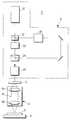
도 1에 나타내는 결정화장치(1)는 프로젝션방식의 조사장치로서, 위상변조소자(2), 조명계(3), 결상광학계(4) 및 기판스테이지(6)를 구비하고 있다. 기판스테이지(6)상에는 피처리기판(5)이 재치되고, 펄스레이저광이 조명계(3)→위상변조소자(2)→결상광학계(4)를 통해서 순서대로 피처리기판(5)에 조사되도록 되어 있다. 피처리기판(5)의 피조사면에는 결정화 대상막으로서의 비단결정 반도체막(예를 들 면 어몰퍼스 실리콘막) 및 캡막(예를 들면 산화실리콘막)이 피복형성되어 있다.A
위상변조소자(2)는 조명계(3)와 결상광학계(4) 사이에 설치되고, 소정의 단차를 가지며, 단차진 곳에서 레이저광선군에 프레넬회절을 일으켜 입사광속의 위상을 변조하는 것이다. 이에 따라 펄스레이저광은 결정화대상막을 최적으로 용융·결정화시키기 위한 소망의 프로파일을 갖게 된다.The
조명계(3)는 피처리기판(5)의 비단결정 반도체막을 용융시키기 위한 에너지광을 출력하는 광원(31)으로서 XeCl엑시머레이저 발진기를 구비하고 있다. 이 광원(31)은 파장이 308nm, 펄스폭(반값폭)이 30ns인 펄스레이저광을 발진하는 고유한 특성을 갖고 있다. 또한, 도 1에 나타내는 예에서는, 광원(31)으로서 XeCl엑시머레이저 발진기의 예에 대해서 설명하지만, 이 이외의 다른 광원으로서 KrF엑시머레이저 발진기, ArF엑시머레이저 발진기 또는 YAG레이저 발진기 등을 이용할 수도 있다.The illumination system 3 includes a XeCl excimer laser oscillator as a
또한, 조명계(3)는 광원(31)에 이어서 광분할수단으로서의 빔스프리터(32), 레이저강도 조정수단으로서의 2개의 감쇠기(33, 35), 광합성수단으로서의 빔스프리터(34), 및 위상변조소자(2)에 대향해서 배치되는 조명광학계(37)를 구비하고 있다. 광원(31)으로부터 출사된 펄스레이저광은 빔스프리터(32)에 의해 P편광성분(P1)과 S편광성분(P2)으로 분할되고, P편광성분(P1)은 광원(31)의 광축을 따라서 직진해서 제1 감쇠기(33)를 통해서 광합성수단으로서의 빔스프리터(34)에 입사되는 한편, S편광성분(P2)은 광원광축에 직교하는 방향으로 진행해서 제2 감쇠기(35)를 통해서 광합성수단으로서의 빔스프리터(34)로 입사된다.The illumination system 3 includes a
이 경우, 직진하는 P편광성분(P1)을 짧은 레이저광로로 통과시켜서 선행시키고, 직교방향의 S편광성분(P2)을 (예를 들면 10m의 광로길이 차를 갖는다)긴 레이저광로로 통과시켜서 전자보다도 약간 늦어지게 한다. P편광성분(P1)과 S편광성분(P2)의 광강도 분포는 피크치를 갖는 정현파상의 광강도 분포이다. 이 P편광성분(P1)에 대한 S편광성분(P2)의 지연시간은 P편광성분(P1)광의 조사영역내에서 감쇠되는 광강도 분포의 위치내에 S편광성분(P2)광을 조사하는 것이다.In this case, the straight P polarized light component P1 is passed through the short laser light path and preceded, and the S polarized light component P2 in the orthogonal direction is passed through the long laser light path (having, for example, an optical path length difference of 10 m) To be a little slower than. The light intensity distribution of the P polarized light component P1 and the S polarized light component P2 is a sine wave light intensity distribution having a peak value. The delay time of the S polarization component P2 with respect to the P polarization component P1 is to irradiate the S polarization component P2 light within the position of the light intensity distribution attenuated in the irradiation region of the P polarization component P1.
이 P편광성분과 S편광성분은 감쇠기 등의 레이저강도 조정수단(33)에 의해 원하는 펄스강도비(P1/P2)로 설정된다. 또한, P편광성분(P1)과 S편광성분(P2)은 예를 들면 편광빔스프리터(34) 등의 광합성수단에 의해 합성되고, 도 2에 나타내는 것과 같이, 폭이 넓은 펄스파형의 합성광(P3)이 된다. 이 합성광(P3)은 1개의 펄스레이저광으로서 위상변조소자 및 결상광학계를 통과하여 최종적으로 피처리기판상의 비단결정 반도체막으로 입사된다.The P-polarized light component and the S-polarized light component are set to a desired pulse intensity ratio (P1 / P2) by a laser intensity adjusting means 33 such as an attenuator. The P polarized light component P1 and the S polarized light component P2 are synthesized by, for example, a photosynthesis means such as a
이 합성광(P3)의 수광면은 용융되고, 펄스레이저광이 차단된 후의 강온기간내의 응고과정에서 결정화된다. 이 경우에, 합성광(P3)의 펄스폭(반값폭)을 기준광 펄스폭(반값폭)의 1.1~2.5배의 범위로 하는 것이 바람직하다. 합성광(P3)의 펄스폭이 1.1배를 하회하면 폭이 넓은 펄스광을 조사한다는 발명의 효과를 잃어버리고, 2.5배를 상회하면 1 펄스광으로서의 집합이 저하되어 균일하게 용융·결정화시킬 수 없어지기 때문이다.The light receiving surface of the composite light P3 is melted and crystallized in the solidification process during the temperature lowering period after the pulsed laser light is cut off. In this case, it is preferable to set the pulse width (half width) of the combined light P3 within a range of 1.1 to 2.5 times the reference light pulse width (half width). If the pulse width of the combined light P3 is less than 1.1 times, the effect of the invention of irradiating a pulse light with a wide width is lost. If the pulse width of the combined light P3 is 2.5 times or more, the aggregation as one pulse light is lowered and can not be uniformly melted and crystallized It is because.
바꿔 말하면, 합성광(P3)의 수광면이란 기판스테이지(6)상에 재치된 피처리기판(5)이 미리 정해진 속도로 예를 들면 X축 방향으로 이동하고 있는 상태에서, 우선 P편광성분(P1)광에 의해 피처리기판(5)을 조사하고, 상기 지연시간 후에, S편광성분(P2)광에 의해 피처리기판(5)을 조사하는 것이다.In other words, the light-receiving surface of the combined light P3 is a light-receiving surface of the P-polarized light component (for example, the light-receiving surface of the combined light P3) in the state in which the
그 결과, 합성광(P3)의 수광면은, 광원으로부터 출사된 레이저광(P)에 의한 수광면보다 도 2에 나타내는 것과 같이 광범위해진다. 이만큼 결정화영역은 넓어진다. 도 2의 광강도 분포는 광합성수단(34)의 출사광의 광강도 분포를 나타내고 있다. 이상의 결과, 레이저광원(31)으로부터 1발의 레이저광으로 큰 결정화영역을 형성할 수 있다.As a result, the light receiving surface of the combined light P3 becomes wider as shown in Fig. 2 than the light receiving surface by the laser light P emitted from the light source. The crystallization zone is enlarged as much as this. The light intensity distribution of FIG. 2 shows the light intensity distribution of the outgoing light of the photosynthesis means 34. As a result, a large crystallization region can be formed from one laser beam from the
도 1에 나타내는 예에서는, 설명상, 펄스레이저광의 광학적 분할·합성수단으로서 2개의 빔스프리터(32, 34)를 이용하고 있지만, 본 발명에서는 펄스레이저광의 광학적 분할·합성수단을 3개 이상, 바람직하게는 3~12개 이용할 필요가 있다. 이와 같이, 3개 이상의 광학적 분할·합성수단을 이용함으로써 보다 펄스폭이 넓은 펄스레이저광을 얻을 수 있다. 또한, 12개를 넘는 광학적 분할·합성수단을 배치하면, 장치가 복잡하면서도 커지고 값이 비싸지므로 바람직하지 않다.In the example shown in Fig. 1, two
광분할·합성수단에는 장치코스트나 성능의 안정성 등을 종합적으로 감안해서 편광빔 스프리터 또는 부분투과미러 또는 이들의 조합에서 선택할 수 있다. 편광빔 스프리터를 이용하는 경우의 광의 분할각도는 5°~175° 범위에서 임의의 값으로 설정할 수 있지만, 장치의 구조가 간단하고, 주변 기기와의 간섭을 고려한 레이아웃설계가 용이하다는 것 등의 이유에서 90°±1°로 하는 것이 바람직하다.The light dividing and synthesizing means can be selected from a polarization beam splitter or a partial transmission mirror or a combination thereof in consideration of the apparatus cost and the stability of performance. The angle of division of light in the case of using a polarization beam splitter can be set to any value in a range of 5 to 175 degrees. However, since the structure of the apparatus is simple and layout designing in consideration of interference with peripheral devices is easy, etc. 90 DEG +/- 1 DEG.
광학적 분할·합성수단으로서 3개 이상, 바람직하게는 3~12개의 부분투과미러를 이용하는 경우, 이 부분투과미러들은 광로상에서 레이저발진기에 가까운 쪽부 터 세서 1번째의 부분투과미러의 반사율(R1)이 0.3 이상 0.6이하이며, 2번째 이하 n번째까지의 부분투과미러의 반사율은, R2〈(R1/3), 또한, R2〈R3〈R3〈R4…〈Rn이며, n번째의 부분투과미러의 후단에 전반사미러가 설치되어 있으며, 인접하는 미러와의 광로길이는 2250mm 이상 5000mm이하로 할 수 있다.When three or more, preferably three to twelve, partial transmitting mirrors are used as the optical dividing / combining means, the partial transmitting mirrors are arranged such that the reflectance R1 of the first partial transmitting mirror on the side closer to the laser oscillator on the optical path is 0.3 or more and 0.6 or less, and the reflection ratios of the partial transmission mirrors of the second through nth partial transmission mirrors satisfy R2 <(R1 / 3) and R2 <R3 <R3 <R4 <Rn, the total reflection mirror is provided at the rear end of the nth partial transmission mirror, and the optical path length with the adjacent mirror can be set at 2250 mm or more and 5000 mm or less.
R1이 0.3미만인 경우는 1번째의 부분반사판에서 반사하는 레이저광의 강도가 약하여 비단결정 반도체막을 용융하기 위해서 필요한 에너지에 도달하지 못해서 효율적이지 않다. R1이 0.6을 넘으면, 2번째 이후의 미러에 도달하는 열을 보충하는 효과가 약해진다. 2번째 이후 n번째까지의 부분투과미러의 반사율을, R2〈(R1/3), 또한, R2〈R3〈R3〈R4…〈Rn으로 함으로써 비단결정 반도체막에서 기판 혹은 캡층으로 확산되는 열을 효과적으로 보충할 수 있다.When R1 is less than 0.3, the intensity of the laser beam reflected by the first partial reflector is weak and it is not efficient because it does not reach the energy required to melt the non-single crystalline semiconductor film. If R1 exceeds 0.6, the effect of supplementing the heat reaching the second and subsequent mirrors is weakened. The reflection ratios of the second through nth partial transmission mirrors are defined as R2 <(R1 / 3), and R2 <R3 <R3 <R4 ... ≪ Rn, the heat diffused from the non-single crystal semiconductor film to the substrate or the cap layer can be effectively supplemented.
부분투과미러를 7장으로 구성하는 경우, 광로상에서 레이저발진기에 가까운 쪽으로부터 세서 n번째의 부분투과미러의 반사율(Rn)은 R1=0.56±0.03, R2=0.07±0.03, R3=0.14±0.03, R4=0.17±0.03, R5=0.25±0.03, R6=0.35±0.03, R7=0.45±0.03으로서, 반사율(R7)의 부분투과미러의 다음에 전반사미러가 배치되어 있으며, 이 7장의 부분투과미러와 1장의 전반사미러는 인접하는 미러와의 광로길이가 4500mm 떨어져 설치되어 있으며, 1번째의 부분투과미러를 투과한 광은 2번째의 부분투과미러로 입사되고, 1번째의 부분투과미러에서 반사한 광은 조명광학계로 도입되고, 2번째의 부분투과미러를 투과한 광은 3번째의 부분투과미러로 입사되고, 2번째의 부분투과미러에서 반사한 광은 1번째의 부분투과미러를 거쳐 조명광학계로 도입되고, 이하, n번째의 부분투과미러를 투과한 광은 n+1번째의 부분투과미러로 도 입되고, n번째의 부분투과미러에서 반사한 광은 n-1, n-2…, 1번째의 부분투과미러를 거쳐 조명광학계로 도입되고, 단 7번째의 부분투과미러를 투과한 광은 전반사미러에서 반사되어 7, 6, …, 1번째의 부분투과미러를 거쳐 조명광학계로 도입되는 것으로 할 수 있다.The reflectance Rn of the nth partial transmitting mirror from the side closer to the laser oscillator on the optical path is R1 = 0.56 +/- 0.03, R2 = 0.07 +/- 0.03, R3 = 0.14 +/- 0.03, The total reflection mirror is disposed after the partial transmission mirror with the reflectance R7 and the partial reflection mirrors are disposed after the partial reflection mirrors with the reflectance R7 and R7 = 0.17 + 0.03, R5 = 0.25 + 0.03, R6 = 0.35 + 0.03, One total reflection mirror is provided with an optical path length of 4500 mm from the adjacent mirror. The light transmitted through the first partial transmission mirror is incident on the second partial transmission mirror, and the light reflected by the first partial transmission mirror The light transmitted through the second partial transmitting mirror enters the third partial transmitting mirror and the light reflected by the second partial transmitting mirror passes through the first partial transmitting mirror to the illumination optical system The light transmitted through the nth partial transmission mirror is introduced into the (n + 1) th Partial transmission mirror also being input to the light reflected by the partial transmission mirror of the n th n-1, n-2 ... , The first partial transmission mirror, and the seventh partial transmission mirror is reflected by the total reflection mirror so as to be transmitted through the seventh, sixth, , And is introduced into the illumination optical system through the first partial transmission mirror.
n번째의 부분투과미러의 반사율(Rn)은 R1=0.40±0.03, R2=0.07±0.03, R3=0.085±0.03, R4=0.095±0.03, R5=0.125±0.03, R6=0.017±0.03, R7=0.25±0.03으로 할 수 있다.The reflectance Rn of the nth partial transmitting mirror is R1 = 0.40 + 0.03, R2 = 0.07 + 0.03, R3 = 0.085 + 0.03, R4 = 0.095 + 0.03, R5 = 0.125 + 0.03, R6 = 0.017 + 0.03, 0.25 0.03.
또, 분할한 레이저광을 합성할 때의 각각의 지연시간으로서는 레이저펄스의 반값 전폭 정도가 바람직하다. 그 이유는, 지연시간이 짧으면 레이저광을 분할·합성하는 효과가 약해지고, 한편, 지연시간이 너무 길어지면, 펄스폭을 확대한 단일 레이저펄스라기 보다도 오히려 복수의 레이저펄스에 가까워지기 때문이다.It is preferable that the delay time when combining the divided laser beams is about half of the full width of the laser pulse. The reason is that if the delay time is short, the effect of dividing and synthesizing the laser light is weakened. On the other hand, if the delay time becomes too long, the laser pulse becomes closer to a plurality of laser pulses rather than a single laser pulse with an enlarged pulse width.
레이저광은 전술한 것과 같이 그 반값 전폭이 15ns에서 30ns정도인 것을 고를 수 있다. 레이저광이 15ns, 30ns로 진행하는 거리는 각각 4500mm, 9000mm이다. 따라서, 인접하는 미러의 광로길이를 2250mm에서 4500mm로 설정하면, 광이 미러 사이를 왕복하는 시간(지연시간)을 15ns에서 30ns로 설정할 수 있다. 5000mm으로 설정했을 경우에는 33ns의 지연시간을 설정할 수 있다.As described above, the laser beam can be selected to have a full width at half maximum of 15 ns to 30 ns. The distances that the laser beam travels for 15 ns and 30 ns are 4500 mm and 9000 mm, respectively. Therefore, if the optical path length of the adjacent mirror is set from 2250 mm to 4500 mm, the time (delay time) in which the light travels between the mirrors can be set to 15 ns to 30 ns. When it is set to 5000 mm, a delay time of 33 ns can be set.
다음으로, 도 3을 참조해서 조명광학계(37)의 상세에 대해서 설명하겠다.Next, details of the illumination
조명광학계(37)에 입사된 합성광(P3)은 빔익스팬더(3a)를 통해서 확대된 후, 제1 플라이아이렌즈(3b)로 입사된다. 이렇게 해서 제1 플라이아이렌즈(3b)의 후측 초점면에는 복수의 소광원이 형성되고, 이 복수의 소광원으로부터의 광속은 제1 컨 덴서 광학계(3c)를 통해서 제2 플라이아이렌즈(3d)의 입사면을 중첩적으로 조명한다. 그 결과, 제2 플라이아이렌즈(3d)의 후측 초점면에는 제1 플라이아이렌즈(3b)의 후측 초점면보다도 많은 복수의 소광원이 형성된다.The combined light P3 incident on the illumination
제2 플라이아이렌즈(3d)의 후측 초점면에 형성된 복수의 소광원으로부터의 광속은 제2 컨덴서광학계(3e)를 통해서 위상변조소자(2)를 중첩적으로 조명한다. 여기서, 제1 플라이아이렌즈(3b) 및 제1 컨덴서광학계(3c)는 제1 호모지나이저를 구성하고, 이 제1 호모지나이저에 의해 광원(31)으로부터 공급된 레이저광에 대해서 위상변조소자(2)상에서의 입사각도에 관한 균일화를 꾀할 수 있다.The light flux from the plurality of small light sources formed on the rear focal plane of the second fly's
제2 플라이아이렌즈(3d) 및 제2 컨덴서광학계(3e)는 제2 호모지나이저를 구성하고, 이 제2 호모지나이저에 의해 제1 호모지나이저로부터의 입사각도가 균일화된 레이저광에 대해서 위상변조소자(2)상에서의 면내 각 위치에서의 광강도에 관한 균일화를 꾀할 수 있다. 이렇게 해서, 조명계(3)는 거의 균일한 광강도 분포를 갖는 레이저광에 의해 위상변조소자(2)를 조명한다.The second fly-
이어서, 위상변조소자(2)에서 위상변조된 레이저광은 역피크 패턴상의 광강도 분포의 광이다. 역피크 패턴상의 광강도 분포란 1발의 레이저광의 빔 직경내에서 최소 광강도값과 최대 광강도값이 연속해서 광강도가 변화되는 분포이다. 최소 광강도값은 피처리기판에서의 비단결정 반도체막의 융점 이하의 온도로 설정된다. 결상광학계(4)를 통해서 피처리기판(5)으로 입사된다.Subsequently, the laser beam phase-modulated by the
여기서, 결상광학계(4)는 위상변조소자(2)의 패턴면과 피처리기판(5)(엄밀하게는 비단결정 반도체막의 상면)을 광학적으로 공역으로 배치하고 있다. 바꿔 말하 면, 피처리기판(5)은 위상변조소자(2)의 패턴면과 광학적으로 공역인 면(결상광학계(4)의 상면)에 설정되어 있다. 결상광학계(4)는 전정렌즈군(4a)과 후정렌즈군(4b)의 사이에 개구조리개(4c)를 구비하고 있다. 개구조리개(4c)는 예를 들면 개구부(광투과부)의 크기가 다른 복수의 개구조리개로 이루어지며, 이 복수의 개구조리개(4c)는 광로에 대해서 교환가능하게 구성되어 있어도 좋다. 또는, 개구조리개(4c)로서 개구부의 크기를 연속적으로 변화시킬 수 있는 홍채조리개를 이용해도 좋다. 어떻게 해도 개구조리개(4c)의 개구부의 크기(더 나아가서는 결상광학계(4)의 상측 개구수(NA))는 후술하는 것과 같이, 피처리기판(5)의 반도체층상에서 소요의 광강도 분포를 발생시키도록 설정되어 있다. 이 결상광학계(4)는 굴절형의 광학계여도 좋고, 반사형의 광학계여도 좋고, 굴절반사형 광학계에도 좋다.Here, the imaging
최종적으로, 합성광(P3)은 피처리기판(5)의 비정질 박막상에 결상된다. 이에 따라, 비정질박막이 용융되고, 응고되는 과정에서 결정화된다. 피처리기판(5)은 예를 들면 액정디스플레이용 판유리기판상에 화학기상성장법(CVD)에 의해 하지막 및 비정질 실리콘막(반도체층) 및 캡막이 순차형성된 것이다. 하지절연막은 절연재, 예를 들면, SiO2로 형성되어 있고, 비정질 실리콘막과 유리기판이 직접 접촉해서 유리기판내의 Na등의 이물질이 비정질 실리콘막에 혼입되는 것을 방지함과 함께, 비정질 실리콘막의 용융온도가 집적 유리기판에 전열되는 것을 방지한다. 비정질 실리콘막은 결정화되는 반도체막으로서, 비단결정막이며 비정질 반도체막이나 다결정 반도체 등이다.Finally, the synthetic light P3 is imaged on the amorphous thin film of the
비단결정막은 상기 반도체막에 한정되지 않고, 비단결정의 금속 등의 비단결정재료로 형성되어 있는 막이어도 좋다. 바람직하게는, 비정질 실리콘막상에는 캡막으로서 절연막 예를 들면 SiO2막이 성막되어 있다. 캡막은 비정질 실리콘막에 입사되는 광빔의 일부에 의해 가열되고, 이 가열된 온도를 축열한다. 이 축열효과는 캡막이 없으면 광빔의 입사가 차단되었을 때, 비정질 실리콘막의 피조사면에서 고온부가 상대적으로 급속히 강온되지만, 이 강온구배를 완화시켜 대입경의 횡방향의 결정성장을 촉진시킨다. 피처리기판(5)은 진공척이나 정전척 등에 의해 기판스테이지(6)상에서 미리 정해진 소정의 위치에 위치결정되어 유지된다.The non-single crystal film is not limited to the semiconductor film but may be a film formed of a non-single crystal material such as a non-single crystal metal. Preferably, an insulating film such as an SiO2 film is formed as a cap film on the amorphous silicon film. The cap film is heated by a part of the light beam incident on the amorphous silicon film and accumulates the heated temperature. The heat storage effect is such that, when the incidence of the light beam is interrupted without the cap film, the high temperature portion is relatively rapidly lowered at the surface to be irradiated of the amorphous silicon film, but this temperature gradient is relaxed to promote the crystal growth in the transverse direction. The
다음으로, 본 발명의 일실시형태에 따른 결정화방법 및 결정화장치의 개략에 대해서 도 4를 참조해서 설명하겠다.Next, the outline of the crystallization method and the crystallization apparatus according to one embodiment of the present invention will be described with reference to Fig.
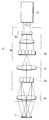
도 4에 나타내는 결정화장치는 레이저광원, 7장의 부분투과미러(R1~R7), 전반사미러, 조명광학계, 위상변조소자, 투영광학계, 및 기판스테이지를 구비하고 있다. 기판스테이지상에는 비단결정 반도체막을 갖는 피처리기판이 재치되어 있다.The crystallization apparatus shown in Fig. 4 has a laser light source, seven partial transmission mirrors R1 to R7, a total reflection mirror, an illumination optical system, a phase modulation element, a projection optical system, and a substrate stage. A substrate to be processed having a non-single crystal semiconductor film is placed on the substrate stage.
레이저광원으로부터의 펄스레이저광이, 부분투과미러 및 전반사미러, 조명광학계, 위상변조소자, 및 투영광학계를 통해서, 피처리기판에 조사되도록 되어 있다.The pulse laser light from the laser light source is irradiated to the substrate to be processed through the partial transmission mirror and the total reflection mirror, the illumination optical system, the phase modulation element, and the projection optical system.
레이저발진기에 의해 발진되는 펄스레이저광으로서는 파장 308nm, 반값 전폭 약 25ns인 XeCl엑시머레이저를 사용했다. 레이저발진기로부터 발진된 레이저광은 7장의 부분투과미러와 1장의 전반사미러와, 이 광학소자들의 서로의 거리와 광로를 적절하게 설정하기 위한 전반사 요면경(凹面鏡)으로 이루어지는 광학장치에 도입된다. 부분투과미러의 반사율(Rn)은 광로상의 위치가 레이저에 가까운 순으로, R1=0.40, R2=0.07, R3=0.085, R4=0.095, R5=0.125, R6=0.17, R7=0.25로 했다. 반사율(R7)의 부분투과미러의 후역에는 전반사미러를 설치했다. 이웃하는 미러와의 광로길이는 4500mm로 했다.As the pulsed laser light oscillated by the laser oscillator, an XeCl excimer laser having a wavelength of 308 nm and a half full width of about 25 ns was used. The laser light emitted from the laser oscillator is introduced into an optical device composed of seven partial transmissive mirrors, one total reflection mirror, and a total reflection peripheral mirror (concave mirror) for appropriately setting the distances and optical paths of the optical elements. The reflectance Rn of the partial transmissive mirror is R1 = 0.40, R2 = 0.07, R3 = 0.085, R4 = 0.095, R5 = 0.125, R6 = 0.17 and R7 = 0.25 in the order of position on the optical path. A total reflection mirror is provided in the rear portion of the partial transmission mirror of reflectance R7. The optical path length to the neighboring mirror was 4500 mm.
또한, 본 실시형태에서는 전반사의 요면경 사이에 부분투과미러를 설치했지만, 요면경 대신에 평판미러를 사용해도 좋고, 도 4에 나타내는 것과 같이, 이 미러들을 이용하지 않고 부분투과미러를 직선적으로 배치해도 좋다.Further, in the present embodiment, the partial transmission mirror is provided between the concave surfaces of the total reflection. However, a flat mirror may be used instead of the concave mirror, or a partial transmission mirror may be linearly arranged without using these mirrors .
이상과 같은 도 4에 나타내는 결정화장치에 있어서, 7장의 부분투과미러에 의한 펄스레이저광의 투과·반사는 다음과 같이 해서 행해진다. 즉, 1번째의 부분투과미러(R1)를 투과한 광은 2번째의 부분투과미러(R2)로 입사되고, 1번째의 부분투과미러(R1)에서 반사한 광은 조명광학계로 도입되고, 2번째의 부분투과미러(R2)를 투과한 광은 3번째의 부분투과미러(R3)로 도입되고, 2번째의 부분투과미러(R2)에서 반사한 광은 1번째의 부분투과미러(R1)를 거쳐서 조명광학계로 도입되고, 이하, n번째의 부분투과미러를 투과한 광은 n+1번째의 부분투과미러로 입사되고, n번째의 부분투과미러에서 반사한 광은 n-1, n-2…, 1번째의 부분투과미러(R1)를 거쳐 조명광학계로 도입된다.In the above-described crystallization apparatus shown in Fig. 4, transmission and reflection of pulsed laser light by seven partial transmission mirrors are performed as follows. That is, the light transmitted through the first partial transmission mirror R1 is incident on the second partial transmission mirror R2, the light reflected by the first partial transmission mirror R1 is introduced into the illumination optical system, The light transmitted through the second partial
또한, 7번째의 부분투과미러(R7)를 투과한 광은 전반사미러에서 반사되어 7, 6, …, 1번째의 부분투과미러를 거쳐 조명광학계로 도입된다.Further, the light transmitted through the seventh partial transmission mirror R7 is reflected by the total reflection mirror 7, 6, ... , And is introduced into the illumination optical system via the first partial transmission mirror.
이와 같은 투과·반사의 반복에 의해 펄스폭은 확장되고, 피처리기판에 대한 조사시간은 연장된다. 그 결과 실리콘막의 온도가 최고에 달했을 시각에 펄스폭을 확장하지 않은 경우보다도 많은 열이 실리콘막으로부터 캡막 및 하지SiO2층으로 확산되고, 이 온도들이 상승하고 있다. 그에 따라 실리콘막의 냉각속도가 느려지고, 실리콘막의 용융시간은 길어져, 결정성장의 거리가 길어진다. 그 결과, 대입경의 결정을 얻을 수 있다.By repeating the transmission and reflection, the pulse width is extended and the irradiation time with respect to the substrate to be processed is extended. As a result, more heat is diffused from the silicon film to the cap film and the underlying SiO2 layer than when the pulse width is not expanded at the time when the temperature of the silicon film reaches the maximum, and these temperatures are rising. As a result, the cooling rate of the silicon film becomes slow, the melting time of the silicon film becomes long, and the distance of crystal growth becomes long. As a result, a large-scale decision can be obtained.
이에 비해, 이와 같은 펄스레이저광의 파형 제어가 되지 않는 경우에는 실리콘막의 온도가 최고로 달한 시각에서 캡막과 하지SiO2층으로 확산되고 있는 열량이 적다. 이 때문에 실리콘막의 냉각속도는 파형제어된 경우에 비해서 빠르고, 따라서 실리콘막의 용융시간이 짧아져 결정성장거리가 짧아진다.On the other hand, when the waveform control of such pulsed laser light can not be performed, the amount of heat diffused into the cap film and the underlying SiO2 layer at the time when the temperature of the silicon film reaches the maximum is small. Therefore, the cooling rate of the silicon film is faster than that in the case of controlling the waveform, so that the melting time of the silicon film is shortened and the crystal growth distance is shortened.
이 모습들을 나타내는 것으로서, 도 5a 및 도 5b에, 레이저광 조사직후의 시료단면의 온도분포를 도시한다. 또한, 도 5a는 펄스레이저광의 파형제어가 되지 않는 경우, 도 5b는 펄스레이저광의 파형제어가 된 경우를 각각 나타낸다.5A and 5B show the temperature distribution of the cross section of the sample just after the laser light irradiation. Fig. 5A shows the case where the pulse laser light is not controlled, and Fig. 5B shows the case where the pulse laser light is controlled.
이하, 본 발명의 실시예를 나타내고, 본 발명에 대해서 구체적으로 설명하겠다.Hereinafter, examples of the present invention will be described, and the present invention will be specifically described.
실시예1Example 1
본 실시예는 펄스레이저광을 사용해서 상면에 캡막을 형성한 비정질 실리콘막을 결정화한 예이다.The present embodiment is an example of crystallizing an amorphous silicon film having a cap film formed on its upper surface by using pulsed laser light.
석영기판상에 PECVD법에 의해 성막한, 막두께 50nm의 비정질 실리콘막을 600℃로 가열하고, 막중의 수소함유량을 줄인 시료를 이용했다. 도 4에 나타내는 것과 같은 결정화장치를 이용해서 7장의 부분투과미러에 의해 파형제어를 행하고, 위상변조소자에 의해 원하는 광강도 분포로 한 펄스레이저광을 시료에 조사하여 비정질 실리콘막을 결정화했다.A 50 nm-thick amorphous silicon film formed by PECVD on a quartz substrate was heated to 600 占 폚 and a hydrogen content in the film was reduced. Waveform control was performed with seven partial transmission mirrors using a crystallization apparatus as shown in Fig. 4, and the amorphous silicon film was crystallized by irradiating the sample with pulsed laser light having a desired light intensity distribution by the phase modulation element.
도 6은, 막두께50nm의 비정질 실리콘막상에 캡막으로서 50nm~550nm의 SiO2막을 성막한 시료에 대해서, 위상변조소자에 의한 V자형 광강도 분포의 펄스레이저광을 조사해서 얻어진 침상 결정의 입자길이(㎛)를 나타내고 있다. 또 같은 도에서는, 뒤에 실시예2에서 설명할 캡층이 없는 시료에 대해서도 그 결과를 나타내고 있다.6 is a graph showing the relationship between the particle length of the acicular crystal obtained by irradiating pulsed laser light having a V-shaped light intensity distribution by a phase modulation device on a sample in which a SiO2 film having a thickness of 50 nm to 550 nm is formed as a cap film on an amorphous silicon film having a film thickness of 50 nm (占 퐉). In the same figure, the results are also shown for a sample having no cap layer to be described later in the second embodiment.
도 6으로부터, 부분투과미러에 의해 파형제어를 행하지 않는 종래 기술에서는 입자길이의 최대는 7.5㎛인 데 비해서, 7장의 부분투과미러에 의해 파형제어를 행한 본 실시예에서는 최대 25㎛의 결정립이 성장하고 있다.6, in the prior art in which the waveform control is not performed by the partial transmission mirror, the maximum grain length is 7.5 m, whereas in this embodiment in which waveform control is performed by seven partial transmission mirrors, .
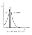
이 현상에 대해서, 비정질 실리콘막상에 550nm의 캡층을 형성한 경우에 대해서 설명하겠다. 도 7a에 시간에 의한 레이저강도의 변화, 즉 펄스파형을 나타내고, 도 7b에 실리콘막의 과도온도 변화를 나타낸다. 이것들은 계산치이며, 또 스케일은 모두 임의눈금이다. 펄스파형은 도 4에서 레이저광이 조명광학계로 입사되는 직전의 위치, 혹은 조명광학계보다 하류의 위치에서, 산란광을 포토다이오드 등의 센서로 검출하고, 그 출력을 고속 오실로스코프로 관측함으로써 측정할 수 있다.In this phenomenon, a case where a cap layer of 550 nm is formed on an amorphous silicon film will be described. Fig. 7A shows a change in laser intensity with time, that is, a pulse waveform, and Fig. 7B shows a change in transient temperature of the silicon film. These are calculated values, and all scales are arbitrary scales. The pulse waveform can be measured by detecting scattered light with a sensor such as a photodiode at a position immediately before the laser light is incident on the illumination optical system or a position downstream of the illumination optical system in FIG. 4, and observing the output with a high-speed oscilloscope .
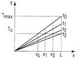
도 7b에 나타내는 실리콘막의 온도는 위상변조소자에 의해 얻은 V자형 광강도에서 광강도가 가장 높은 곳의 온도를 나타내고 있다. 온도가 최고에 달하면, 광 강도가 가장 약한 곳, 즉 약 50%의 광강도 부분에서 결정핵이 발생하고, 횡방향 결정성장을 개시한다. 또한 결정핵이 발생하는 위치는 실리콘막이 완전용융되는 임계치에 상당한다.The temperature of the silicon film shown in Fig. 7B indicates the temperature where the light intensity is highest at the V-shaped light intensity obtained by the phase modulation element. When the temperature reaches the maximum, crystal nuclei are generated in a portion where the light intensity is the weakest, that is, about 50% of the light intensity portion, and the lateral crystal growth starts. The position at which crystal nuclei are generated corresponds to a threshold at which the silicon film is completely melted.
본 실시예에서는, 횡방향성장이 개시한 후에도 소정시간, 펄스레이저광의 강도가 유지되고 있는 것을 도 7a 및 도 7b로부터 알 수 있다. 그 사이, 실리콘막으로부터 기판 및 캡층에 대한 열의 확산이 생기지만, 그 열을 보충해야 하는 펄스레이저광이 조사되도록, 부분투과미러의 투과율을 설정하고 있다.In the present embodiment, it can be seen from Figs. 7A and 7B that the intensity of the pulse laser light is maintained for a predetermined time even after the lateral growth starts. In the meantime, the transmittance of the partial transmission mirror is set so that heat is diffused from the silicon film to the substrate and the cap layer, but pulse laser light to be supplemented with the heat is emitted.
이와 같이, 펄스레이저광의 조사시간이 길기 때문에, 실리콘막의 온도가 최고에 달한 후의 실리콘막의 냉각속도는 파형제어를 하지 않는 종래기술에 비교해서 늦어진다. 그 때문에, 실리콘막의 용융시간이 종래기술보다도 길어지고, 결정성장의 거리가 길어진다.As described above, since the irradiation time of the pulsed laser light is long, the cooling rate of the silicon film after reaching the maximum temperature of the silicon film is delayed as compared with the prior art in which the waveform control is not performed. Therefore, the melting time of the silicon film becomes longer than that of the prior art, and the distance of crystal growth becomes longer.
실리콘막의 온도가 내려감과 동시에 결정성장이 진행되지만, 펄스레이저광의 V자형 광강도에서 광강도가 가장 높은 곳의 온도가, 실리콘막이 완전용융되는 임계치까지 내려가는 곳에서 랜덤한 핵발생이 생기고, 횡방향의 결정성장이 정지된다.The crystal growth progresses at the same time as the temperature of the silicon film is lowered. However, random nucleation occurs at a position where the light intensity is highest at the V-shaped light intensity of the pulsed laser light to a threshold at which the silicon film is completely melted, Is stopped.
이상으로부터, 도 7b를 이용해서 결정성장의 시간을 구할 수 있다. 문헌(Y.Takami et.al 210th ECS(2006)E-15(TFT-8))에서 결정성장속도를 13m/s로 가정하면, 결정성장거리는 약 22㎛가 되어 도 6에 나타내는 결과와 잘 일치한다.From the above, the time for crystal growth can be obtained using Fig. 7B. Assuming a crystal growth rate of 13 m / s in the literature (Y.Takami et al 210th ECS (2006) E-15 (TFT-8)), the crystal growth distance becomes about 22 탆, do.
한편, 도 8에, 파형제어를 행하지 않는 종래기술에서의 실리콘막의 과도온도 변화를 나타내고 있다. 본 실시예와 같은 계산을 하면, 결정성장거리는 약 7.5㎛로 구해져 도 6에 나타내는 결과와 거의 합치한다. 또한, 도 8의 횡축은 임의단위지 만, 도 7b의 횡축과 대응하고 있다.On the other hand, Fig. 8 shows the transient temperature change of the silicon film in the prior art in which the waveform control is not performed. When the calculation is performed in the same manner as in the present embodiment, the crystal growth distance is found to be about 7.5 mu m, which is almost the same as the result shown in Fig. The horizontal axis in Fig. 8 corresponds to the horizontal axis in Fig.
앞에서 서술한 것과 같이, 도 6은 V자형 광강도 분포를 이용한 경우의 결정입자 길이를 나타내고 있다. 본 발명자들은 위상변조소자로 형성한 V자형 광강도 분포 대신에, 메탈마스크로 형성한 스텝형 광강도 분포에 대해서도 같은 실험을 해서 캡층이 있는 경우와 없는 경우의 결정립 길이를 조사했다. 그 결과, 캡층이 있는 시료에 대해서 스텝형 광강도 분포의 펄스를 조사한 경우에는 펄스파형 제어를 하지 않는 경우에 2.8㎛, 펄스파형제어를 한 경우에 9㎛가 되었다.As described above, FIG. 6 shows the crystal grain length when the V-shaped light intensity distribution is used. Instead of the V-shaped light intensity distribution formed by the phase modulation device, the present inventors conducted the same experiment on the stepped light intensity distribution formed by the metal mask to examine the crystal grain length with and without the cap layer. As a result, in the case of irradiating the sample having the cap layer with the pulse of the step type light intensity distribution, it was 2.8 占 퐉 when the pulse waveform control was not performed, and 9 占 퐉 when the pulse waveform control was performed.
이상과 같이, 위상변조소자를 이용한 경우에는 메탈마스크에 의해서 스텝상의 광강도 분포를 형성한 경우에 비해서 2배 이상 긴 결정립을 얻을 수 있었다. 이 이유를 도 9a~9d를 이용해서 설명하겠다. 도 9a 및 도 9b는 위상변조소자를 이용한 경우의 광강도 분포, 및 과도온도 변화를 각각 나타내고 있다. 도 9c 및 도 9d는 메탈마스크를 사용한 경우의 광강도 분포와 과도온도 변화를 각각 나타내고 있다.As described above, in the case of using the phase modulation element, a crystal grain longer than twice as long as that in the case where the light intensity distribution in the step was formed by the metal mask was obtained. This reason will be explained using Figs. 9A to 9D. 9A and 9B show the light intensity distribution and the transient temperature change when the phase modulation element is used, respectively. 9C and 9D show light intensity distributions and transient temperature changes when a metal mask is used, respectively.
위상변조소자를 이용한 경우에는 시각(t0)에서, x=xc의 온도가 결정핵 발생의 임계온도(Tc,x=L)의 온도가 실리콘막의 최고온도(Tmax)로 되어 있다. 시각이 t1, t2, t3로 진행함에 따라서 광강도 분포가 약해지는 모습을 나타내고 있다. 과도온도변화를 나타내는 도에서는, x=xc, x1, x2, L에서의 온도의 시간적 변화를 나타내고 있다. 위상변조소자를 이용한 경우에는 시각(t0)에 위치(xc)에서 발생한 결정핵으로부터 결정이 횡방향성장을 개시하고, 시각(t1)에서는 위치(x1)까지 결정성장하고 있 다. 시각이 지남에 따라서 결정이 성장하고, 위치(L)의 온도가 Tc로 내려가는 시각(t3)까지 결정성장이 지속된다. 즉, 결정입자는 시각 t0에서 t3에 걸쳐서 성장한다.When the phase modulation device is used, the temperature of x = xc at the time t0 , and the temperature at the critical temperature (Tc ,x = L) of crystal nucleation is the maximum temperature Tmax of the silicon film. And the light intensity distribution becomes weak as the time progresses to t1 , t2 , and t3 . The diagram showing the transient temperature change shows the temporal change of the temperature at x = xc , x1 , x2 , L. When a phase modulation device is used, crystals start to grow laterally from a crystal nucleus generated at a position (xc ) at a time (t0 ) and grow to a position (x1 ) at a time (t1 ). The crystal grows as the time passes and the crystal growth continues until the time (t3 ) at which the temperature of the position (L) falls to Tc . That is, the crystal grain grows from time t0 to time t3 .
한편, 메탈마스크를 사용한 경우에는, 시각(t0)에서 위치(Xc)의 온도가 Tc이 되고, 위치(x1, x2, x3)의 온도는 Tmax가 되어 있다. 시각(t0)에 위치(xc)에서 발생한 결정핵은 온도가 높은 방향(같은 도의 오른쪽)으로 향해서 성장하려고 하지만, 시각(t1)에서는 x1에서의 온도는 당연히 Tc보다도 높고, 고화될 수 없다, 즉 횡방향으로 결정성장할 수 없다. 위치(x1)의 온도가 Tc까지 내려가는 것은 시각(t3)으로서, 이 시각에서 겨우 결정이 위치(x1)까지 성장한다. 그러나 시각(t3)에는 위치(x2, x3)의 온도가 Tc까지 내려가 있다. 따라서, 이 x2, x3들의 위치에서는 랜덤한 핵 발생이 생기고, 미소한 결정립이 다수 발생하여, 횡방향 성장은 종료되어 버린다.On the other hand, when the metal mask is used, the temperature of the position (Xc ) becomes Tc and the temperature of the position (x1 , x2 , x3 ) becomes Tmax at the time t0 . At the time (t0), nucleation occurs at a position (xc) to try to temperature is grown toward a higher direction (degrees right of the same), but the time (t1) the temperature of the x1 is of course higher than the Tc, solidification It can not grow in the lateral direction. It is the time t3 that the temperature of the position (x1 ) falls to Tc , at which time crystals grow to the position (x1 ). At time t3 , however, the temperature at position (x2 , x3 ) drops to Tc . Therefore, at the positions of x2 and x3 , random nucleation occurs, a lot of fine grains are generated, and the lateral growth is completed.
이와 같이, 위상변조소자를 사용한 경우는 메탈마스크를 사용한 경우에 비해서 횡방향성장의 거리를 늘릴 수 있다.Thus, in the case of using a phase modulation element, the distance of lateral growth can be increased as compared with the case of using a metal mask.
실시예2Example 2
본 실시예에서는 비정질 실리콘막의 상부에 캡막을 설치하지 않는 것을 빼고 본 실시예1과 동일하게 해서 비정질 실리콘막을 결정화했다.In this embodiment, the amorphous silicon film is crystallized in the same manner as in the first embodiment except that the cap film is not provided on the amorphous silicon film.
그 결과, 도 6에 나타내는 것과 같이 파형 제어를 행하지 않는 종래기술의 펄스레이저로 결정화한 경우, 입자 길이 약 2.5㎛의 결정립밖에 얻을 수 없었다. 한편, 본 실시예에서는 결정립의 입자길이는 약 11㎛였다.As a result, as shown in Fig. 6, when crystallized by a pulse laser of the prior art which does not perform waveform control, only a crystal grain having a grain length of about 2.5 mu m could be obtained. On the other hand, in this embodiment, the grain length of the crystal grain was about 11 mu m.
실시예1과 동일하게, 본 실시예와 종래기술의 경우에 대해서 결정성장거리를 계산한 결과, 종래기술에서는 약 2㎛, 본 실시예에서는 13㎛가 되어, 도 6의 결과와 잘 일치했다.As in the case of the first embodiment, the crystal growth distance in the case of this embodiment and the prior art was calculated and found to be about 2 탆 in the conventional technology and 13 탆 in the present embodiment.
이와 같이, 본 실시예에 의하면, 엑시머레이저를 이용한 결정화에서, 캡층을 설치하지 않는 경우에도 입자길이 10㎛이상의 결정립이 얻어지는 것을 알 수 있다. 종래, TFT를 제작하는 경우에는 결정화한 후에는 캡층을 에칭으로 박리하고 제거하는 공정이 필요했다. 그러나, 본 실시예에 의하면, 캡층이 없어도 대입경의 결정립을 형성할 수 있으므로, 캡층을 성막하는 공정과, 결정화 후에 이것을 제거하는 공정은 불필요하다. 이것은 TFT나 그것을 이용한 LCD, OLED 등의 제품의 양산에서 제조비나 수율면에서 상당히 유리하다.As described above, according to the present embodiment, it is understood that, in the case of crystallization using an excimer laser, even when a cap layer is not provided, crystal grains having a particle size of 10 mu m or more can be obtained. Conventionally, in the case of manufacturing a TFT, after the crystallization, a step of peeling and removing the cap layer by etching is required. However, according to this embodiment, crystal grains of a large diameter can be formed even without a cap layer, so that a step of forming a cap layer and a step of removing it after crystallization are unnecessary. This is advantageous in terms of manufacturing cost and yield in mass production of TFTs and LCD and OLED products using the same.
실시예1, 2에서 나타낸 것과 같이, 캡막의 유무에 따라서 결정성장이 다르다. 이것은 도 10에 의해서 이해할 수 있다. 즉, 캡막이 없는 경우(도 10a)에는 실리콘막에 흡수된 열은 하지SiO2측(기판측)에만 확산된다. 한편 캡막이 있는 경우(도 10b)에는 실리콘막에 흡수된 열이 캡막과 하지SiO2의 양쪽에 확산된다. 캡막에 확산된 열은 시간이 경과하면 다시 실리콘막으로 확산된다. 이 때문에, 캡막이 있는 경우 쪽이 실리콘막의 용융시간이 길어져 결정입자 길이가 길어진다.As shown in Examples 1 and 2, crystal growth varies depending on the presence or absence of a cap film. This can be understood from FIG. That is, when there is no cap film (Fig. 10A), the heat absorbed by the silicon film is diffused only to the underlying SiO2 side (substrate side). On the other hand, when the cap film is present (FIG. 10B), heat absorbed in the silicon film diffuses to both the cap film and the underlying SiO2 . The heat diffused into the cap film diffuses back into the silicon film after a lapse of time. Therefore, when the cap film is present, the melting time of the silicon film becomes longer, and the crystal grain length becomes longer.
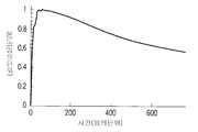
실시예1, 2에서 나타낸 캡막의 유무의 각 경우에서, 결정입자 길이의 에너지 밀도 의존성을 도 11에 나타낸다. 캡막 550nm의 경우에서 20㎛ 이상의 결정립을 얻도록 한 경우에는 에너지밀도 마진은 150mJ/cm2 이상이다. 동일하게, 캡막이 없는 경우에서 10㎛ 이상의 결정립을 얻도록 한 경우의 에너지밀도 마진도 150mJ/cm2 이상이다. 따라서, 레이저의 펄스마다의 에너지 불균일에 대해서도 충분한 마진을 갖는다고 생각할 수 있다.The energy density dependency of the crystal grain length in each case of the presence or absence of the cap film shown in Examples 1 and 2 is shown in Fig. In the case of obtaining a crystal grains of 20 m or more in the case of a cap film of 550 nm, the energy density margin is 150 mJ / cm2 or more. Similarly, the energy density margin2 over 150mJ / cm in the case where to obtain 10㎛ or more crystal grains in the case without the cap film. Therefore, it can be considered that even with respect to energy nonuniformity per pulse of the laser, there is a sufficient margin.
실시예1, 2에서 나타낸 캡막의 유무의 각 경우의 결정에 대해서, SEM이미지 및 SEM-EBSP해석을 한 결과, 파형제어를 한 경우에는 파형제어를 하지 않은 경우에 비해서 1차원 결정(침상 결정)의 입자폭이 넓다는 것을 알았다.As a result of SEM image and SEM-EBSP analysis for the determination of the presence or absence of the cap film shown in Examples 1 and 2, it was found that when waveform control was performed, one-dimensional crystal (needle crystal) The particle width of the particles was wide.
실시예3Example 3
본 실시예에서는 대입경으로 성장하는 결정립에 대해서, 그 결정핵의 발생을 제어하고, 결정립이 2차원적인 퍼짐을 갖는 것에 관한 것이다.The present embodiment relates to crystal grains grown on a large scale by controlling the generation of crystal nuclei and having crystal grains having a two-dimensional spread.
막두께 50nm의 비정질 실리콘막의 상면에 캡층으로서 550nm의 SiO2를 형성한 시료를 사용해 결정립이 2차원적으로 성장하도록 설계한 위상변조소자를 사용한 것을 빼고 실시예1과 동일하게 해서 비정질 실리콘막을 결정화했다.The amorphous silicon film was crystallized in the same manner as in Example 1 except that a phase modulation device designed to grow crystal grains in two dimensions using a sample in which 550 nm of SiO2 was formed as a cap layer on the upper surface of a 50 nm thick amorphous silicon film .
결정립이 2차원적으로 성장한다는 것은 단일의 결정핵으로부터 성장을 개시한 결정립이 2차원적으로 성장하여, 의사적인 단결정으로 간주할 수 있다는 것이다. 파형제어를 하지 않은 종래기술에서 이와 같은 위상변조소자를 사용하면, 예를 들면 5㎛각 정도의 크기의 결정립이 형성된다. 이에 비해서, 본 실시예에서의 파형제어를 한 펄스레이저를 조사하면, 5㎛×20㎛, 또는 20㎛×20㎛ 정도의 결정립을 형성할 수 있다. 도 12에 일예로서 5㎛×10㎛의 결정립의 SEM상을 나타낸다.The fact that crystal grains grow two-dimensionally means that grains that start to grow from a single crystal nucleus grow two-dimensionally and can be regarded as a pseudo-single crystal. When such a phase modulation element is used in the prior art without wave form control, for example, a crystal grain size of about 5 탆 square is formed. On the other hand, by irradiating the pulsed laser with the waveform control in this embodiment, crystal grains of about 5
또한, 캡층이 없는 시료구조에서도 침상 결정으로 결정입자 직경이 확대된 것과 동일하게 2차원적인 의사단결정의 입자 직경을 확대할 수 있다.Further, even in the sample structure without the cap layer, the particle diameter of the two-dimensional pseudo-single crystal can be enlarged like the case where the crystal grain diameter is enlarged by the needle crystal.
이와 같이, 본 실시예에 의하면, 실시예1, 2에서 나타낸 것과 같은 1차원의 침상 결정만이 아니라, 2차원의 의사단결정 실리콘의 입자 직경확대에도 효과가 있다. 1차원 결정인지 2차원 결정인지의 선택, 혹은 그 결정 사이즈의 선택은 위상변조소자의 설계에 의해 자유롭게 변경할 수 있다.As described above, according to this embodiment, not only one-dimensional needle crystals shown in Examples 1 and 2 but also two-dimensional pseudocrystalline silicon are effective for increasing the particle diameter. Selection of one-dimensional crystal or two-dimensional crystal, or selection of crystal size thereof can be freely changed by designing a phase modulation element.
도 1은, 본 발명의 기본적 원리를 설명하기 위한 펄스레이저 조사에 의한 결정화장치의 전체 개요를 나타내는 구성 블럭도이다.BRIEF DESCRIPTION OF DRAWINGS FIG. 1 is a structural block diagram showing the entire outline of a crystallization apparatus by pulsed laser irradiation for explaining the basic principle of the present invention. FIG.
도 2는, 분할 및 합성된 펄스레이저광의 광강도 분포를 나타내는 도이다.Fig. 2 is a diagram showing a light intensity distribution of segmented and synthesized pulsed laser light. Fig.
도 3은, 도 1에 나타내는 장치의 광학계를 나타내는 구성블럭도이다.3 is a block diagram showing the optical system of the apparatus shown in Fig.
도 4는, 본 발명의 일실시형태에 따른 결정화장치를 나타내는 구성블럭도이다.4 is a block diagram showing a crystallization apparatus according to an embodiment of the present invention.
도 5a 및 도 5b는, 레이저조사후의 시료단면의 온도분포를 나타내는 도이다.5A and 5B are diagrams showing the temperature distribution of the sample cross section after laser irradiation.
도 6은, 비정질 실리콘막상의 캡막의 막두께와, 펄스레이저광을 조사해서 얻어진 침상 결정의 입자길이(㎛)의 관계를 나타내는 특성도이다.Fig. 6 is a characteristic diagram showing the relationship between the film thickness of the cap film on the amorphous silicon film and the particle length (mu m) of acicular crystals obtained by irradiation with pulsed laser light.
도 7a 및 도 7b는, 실시예1에서의 시간에 의한 레이저강도 및 실리콘막의 온도 변화를 나타내는 특성도이다.7A and 7B are characteristic diagrams showing changes in laser intensity and temperature of the silicon film with time in the first embodiment.
도 8은, 실시예1에서의 펄스레이저광의 조사에 의한 실리콘막의 온도변화를 나타내는 특성도이다.8 is a characteristic diagram showing the temperature change of the silicon film by irradiation with the pulsed laser light in the first embodiment.
도 9a 내지 도 9d는, 위상변조소자 및 메탈마스크를 사용했을 경우의 광강도 분포와 과도온도변화를 나타내는 도면이다.9A to 9D are diagrams showing the light intensity distribution and the transient temperature change when the phase modulation element and the metal mask are used.
도 10a 및 도 10b는, 캡막이 있는 경우와 없는 경우의 시료단면의 과도온도분포를 나타내는 도면이다.10A and 10B are diagrams showing the transient temperature distribution of a sample cross section with and without a cap film.
도 11은, 파형제어된 경우의 1차원 결정의 입자길이와 레이저의 에너지밀도의 관계를 나타내는 도면이다.11 is a diagram showing the relationship between the particle length of one-dimensional crystal and the energy density of the laser when the waveform is controlled.
도 12는, 실시예3에서의 단일성장핵으로부터 성장한 2차원 결정의 SEM상이다.12 is an SEM image of a two-dimensional crystal grown from single growth nuclei in Example 3. Fig.
Claims (15)
Translated fromKoreanApplications Claiming Priority (2)
| Application Number | Priority Date | Filing Date | Title |
|---|---|---|---|
| JPJP-P-2007-00228128 | 2007-09-03 | ||
| JP2007228128AJP5371220B2 (en) | 2007-09-03 | 2007-09-03 | Crystallization method and crystallizer |
Publications (2)
| Publication Number | Publication Date |
|---|---|
| KR20090024087A KR20090024087A (en) | 2009-03-06 |
| KR101491043B1true KR101491043B1 (en) | 2015-02-06 |
Family
ID=40408134
Family Applications (1)
| Application Number | Title | Priority Date | Filing Date |
|---|---|---|---|
| KR20080086341AExpired - Fee RelatedKR101491043B1 (en) | 2007-09-03 | 2008-09-02 | Crystallization method and apparatus |
Country Status (3)
| Country | Link |
|---|---|
| US (1) | US7727913B2 (en) |
| JP (1) | JP5371220B2 (en) |
| KR (1) | KR101491043B1 (en) |
Families Citing this family (5)
| Publication number | Priority date | Publication date | Assignee | Title |
|---|---|---|---|---|
| TW200422749A (en)* | 2003-04-22 | 2004-11-01 | Adv Lcd Tech Dev Ct Co Ltd | Crystallization apparatus, crystallization method, phase modulation element, device and display apparatus |
| DE102014201739B4 (en)* | 2014-01-31 | 2021-08-12 | Trumpf Laser- Und Systemtechnik Gmbh | Laser processing device and method for generating two partial beams |
| JP6706155B2 (en)* | 2016-06-15 | 2020-06-03 | 株式会社日本製鋼所 | Method for manufacturing polycrystalline semiconductor film, laser annealing device, thin film transistor, and display |
| US12255273B2 (en)* | 2019-02-15 | 2025-03-18 | Samsung Display Co., Ltd. | Display device and method for fabricating the same |
| KR20230024468A (en)* | 2021-08-11 | 2023-02-21 | 삼성전자주식회사 | Apparatus for laser annealing and operating method thereof |
Citations (3)
| Publication number | Priority date | Publication date | Assignee | Title |
|---|---|---|---|---|
| JPH1174216A (en)* | 1997-08-29 | 1999-03-16 | Japan Steel Works Ltd:The | Pulse light irradiation method and pulse light irradiation device |
| JP2005317938A (en)* | 2004-03-31 | 2005-11-10 | Advanced Lcd Technologies Development Center Co Ltd | Device for crystallization, method for crystallization, device, optical modulating element, and display device |
| KR20060046344A (en)* | 2004-06-04 | 2006-05-17 | 가부시키가이샤 에키쇼센탄 기쥬쓰 가이하쓰센타 | Crystallization method, thin film transistor manufacturing method, thin film transistor and display device |
Family Cites Families (7)
| Publication number | Priority date | Publication date | Assignee | Title |
|---|---|---|---|---|
| CA2256699C (en)* | 1996-05-28 | 2003-02-25 | The Trustees Of Columbia University In The City Of New York | Crystallization processing of semiconductor film regions on a substrate, and devices made therewith |
| US6961117B2 (en)* | 2000-11-27 | 2005-11-01 | The Trustees Of Columbia University In The City Of New York | Process and mask projection system for laser crystallization processing of semiconductor film regions on a substrate |
| JP2002280322A (en)* | 2001-03-15 | 2002-09-27 | Ishikawajima Harima Heavy Ind Co Ltd | Laser irradiation device and laser irradiation method |
| TWI227913B (en)* | 2003-05-02 | 2005-02-11 | Au Optronics Corp | Method of fabricating polysilicon film by excimer laser crystallization process |
| TWI239936B (en)* | 2004-02-27 | 2005-09-21 | Au Optronics Corp | Laser annealing apparatus and laser annealing method |
| TW200541078A (en)* | 2004-03-31 | 2005-12-16 | Adv Lcd Tech Dev Ct Co Ltd | Crystallization apparatus, crystallization method, device, optical modulation element, and display apparatus |
| JP4769491B2 (en) | 2004-06-04 | 2011-09-07 | 株式会社 液晶先端技術開発センター | Crystallization method, thin film transistor manufacturing method, thin film transistor, and display device |
- 2007
- 2007-09-03JPJP2007228128Apatent/JP5371220B2/enactiveActive
- 2008
- 2008-09-02KRKR20080086341Apatent/KR101491043B1/ennot_activeExpired - Fee Related
- 2008-09-02USUS12/202,651patent/US7727913B2/ennot_activeExpired - Fee Related
Patent Citations (3)
| Publication number | Priority date | Publication date | Assignee | Title |
|---|---|---|---|---|
| JPH1174216A (en)* | 1997-08-29 | 1999-03-16 | Japan Steel Works Ltd:The | Pulse light irradiation method and pulse light irradiation device |
| JP2005317938A (en)* | 2004-03-31 | 2005-11-10 | Advanced Lcd Technologies Development Center Co Ltd | Device for crystallization, method for crystallization, device, optical modulating element, and display device |
| KR20060046344A (en)* | 2004-06-04 | 2006-05-17 | 가부시키가이샤 에키쇼센탄 기쥬쓰 가이하쓰센타 | Crystallization method, thin film transistor manufacturing method, thin film transistor and display device |
Also Published As
| Publication number | Publication date |
|---|---|
| US7727913B2 (en) | 2010-06-01 |
| JP2009060041A (en) | 2009-03-19 |
| US20090061603A1 (en) | 2009-03-05 |
| KR20090024087A (en) | 2009-03-06 |
| JP5371220B2 (en) | 2013-12-18 |
Similar Documents
| Publication | Publication Date | Title |
|---|---|---|
| US9058994B2 (en) | Laser annealing method and device | |
| US7943936B2 (en) | Crystallizing method, thin-film transistor manufacturing method, thin-film transistor, and display device | |
| JP2000068520A (en) | Semiconductor thin film, method of manufacturing the same, manufacturing apparatus, semiconductor element, and method of manufacturing the same | |
| TWI549164B (en) | Laser annealing method and apparatus | |
| KR101491043B1 (en) | Crystallization method and apparatus | |
| KR20060048219A (en) | Method for manufacturing semiconductor thin film and apparatus for manufacturing semiconductor thin film | |
| KR20080103390A (en) | Crystallization Apparatus and Crystallization Method | |
| KR100913618B1 (en) | Crystallization apparatus and crystallization method | |
| US20090038536A1 (en) | Crystallization apparatus, crystallization method, device, optical modulation element, and display apparatus | |
| US7998841B2 (en) | Method for dehydrogenation treatment and method for forming crystalline silicon film | |
| KR20060048396A (en) | Method and apparatus for manufacturing semiconductor thin film | |
| JP2002261015A (en) | Semiconductor thin film, method for manufacturing the same, manufacturing apparatus, semiconductor element, and method for manufacturing the same | |
| TW588128B (en) | Method and apparatus for forming a semiconductor thin film | |
| JPWO2012029488A1 (en) | Laser annealing apparatus and laser annealing method | |
| JP2009130231A (en) | Crystal silicon array and method for manufacturing thin film transistor | |
| KR100619197B1 (en) | Crystal growth apparatus and crystal growth method for semiconductor thin film | |
| JP2005317938A (en) | Device for crystallization, method for crystallization, device, optical modulating element, and display device | |
| JP2006295097A (en) | Crystallizing method, thin-film transistor manufacturing method, crystallized substrate, thin-film transistor, and display device | |
| JPH09213651A (en) | Semiconductor thin film manufacturing apparatus and semiconductor thin film manufacturing method | |
| JP2001176797A (en) | Method and apparatus for manufacturing thin-film semiconductor device | |
| JP4377442B2 (en) | Semiconductor thin film forming method, semiconductor thin film forming apparatus, crystallization method and crystallization apparatus | |
| JP2007005412A (en) | Method of forming polysilicon film | |
| JP2002198313A (en) | Method for forming semiconductor thin film, pulse laser radiation apparatus and semiconductor device |
Legal Events
| Date | Code | Title | Description |
|---|---|---|---|
| PA0109 | Patent application | St.27 status event code:A-0-1-A10-A12-nap-PA0109 | |
| PG1501 | Laying open of application | St.27 status event code:A-1-1-Q10-Q12-nap-PG1501 | |
| R18-X000 | Changes to party contact information recorded | St.27 status event code:A-3-3-R10-R18-oth-X000 | |
| N231 | Notification of change of applicant | ||
| P11-X000 | Amendment of application requested | St.27 status event code:A-2-2-P10-P11-nap-X000 | |
| P13-X000 | Application amended | St.27 status event code:A-2-2-P10-P13-nap-X000 | |
| PN2301 | Change of applicant | St.27 status event code:A-3-3-R10-R13-asn-PN2301 St.27 status event code:A-3-3-R10-R11-asn-PN2301 | |
| A201 | Request for examination | ||
| PA0201 | Request for examination | St.27 status event code:A-1-2-D10-D11-exm-PA0201 | |
| D13-X000 | Search requested | St.27 status event code:A-1-2-D10-D13-srh-X000 | |
| D14-X000 | Search report completed | St.27 status event code:A-1-2-D10-D14-srh-X000 | |
| E902 | Notification of reason for refusal | ||
| PE0902 | Notice of grounds for rejection | St.27 status event code:A-1-2-D10-D21-exm-PE0902 | |
| E13-X000 | Pre-grant limitation requested | St.27 status event code:A-2-3-E10-E13-lim-X000 | |
| P11-X000 | Amendment of application requested | St.27 status event code:A-2-2-P10-P11-nap-X000 | |
| P13-X000 | Application amended | St.27 status event code:A-2-2-P10-P13-nap-X000 | |
| N231 | Notification of change of applicant | ||
| PN2301 | Change of applicant | St.27 status event code:A-3-3-R10-R13-asn-PN2301 St.27 status event code:A-3-3-R10-R11-asn-PN2301 | |
| P11-X000 | Amendment of application requested | St.27 status event code:A-2-2-P10-P11-nap-X000 | |
| P13-X000 | Application amended | St.27 status event code:A-2-2-P10-P13-nap-X000 | |
| E701 | Decision to grant or registration of patent right | ||
| PE0701 | Decision of registration | St.27 status event code:A-1-2-D10-D22-exm-PE0701 | |
| GRNT | Written decision to grant | ||
| PR0701 | Registration of establishment | St.27 status event code:A-2-4-F10-F11-exm-PR0701 | |
| PR1002 | Payment of registration fee | St.27 status event code:A-2-2-U10-U11-oth-PR1002 Fee payment year number:1 | |
| PG1601 | Publication of registration | St.27 status event code:A-4-4-Q10-Q13-nap-PG1601 | |
| FPAY | Annual fee payment | Payment date:20180126 Year of fee payment:4 | |
| PR1001 | Payment of annual fee | St.27 status event code:A-4-4-U10-U11-oth-PR1001 Fee payment year number:4 | |
| PR1001 | Payment of annual fee | St.27 status event code:A-4-4-U10-U11-oth-PR1001 Fee payment year number:5 | |
| PR1001 | Payment of annual fee | St.27 status event code:A-4-4-U10-U11-oth-PR1001 Fee payment year number:6 | |
| PR1001 | Payment of annual fee | St.27 status event code:A-4-4-U10-U11-oth-PR1001 Fee payment year number:7 | |
| PC1903 | Unpaid annual fee | St.27 status event code:A-4-4-U10-U13-oth-PC1903 Not in force date:20220203 Payment event data comment text:Termination Category : DEFAULT_OF_REGISTRATION_FEE | |
| PC1903 | Unpaid annual fee | St.27 status event code:N-4-6-H10-H13-oth-PC1903 Ip right cessation event data comment text:Termination Category : DEFAULT_OF_REGISTRATION_FEE Not in force date:20220203 |