KR101488521B1 - Semiconductor device - Google Patents
Semiconductor deviceDownload PDFInfo
- Publication number
- KR101488521B1 KR101488521B1KR1020137017757AKR20137017757AKR101488521B1KR 101488521 B1KR101488521 B1KR 101488521B1KR 1020137017757 AKR1020137017757 AKR 1020137017757AKR 20137017757 AKR20137017757 AKR 20137017757AKR 101488521 B1KR101488521 B1KR 101488521B1
- Authority
- KR
- South Korea
- Prior art keywords
- transistor
- oxide semiconductor
- potential
- electrode
- semiconductor layer
- Prior art date
- Legal status (The legal status is an assumption and is not a legal conclusion. Google has not performed a legal analysis and makes no representation as to the accuracy of the status listed.)
- Active
Links
Images


Classifications
- H—ELECTRICITY
- H10—SEMICONDUCTOR DEVICES; ELECTRIC SOLID-STATE DEVICES NOT OTHERWISE PROVIDED FOR
- H10F—INORGANIC SEMICONDUCTOR DEVICES SENSITIVE TO INFRARED RADIATION, LIGHT, ELECTROMAGNETIC RADIATION OF SHORTER WAVELENGTH OR CORPUSCULAR RADIATION
- H10F39/00—Integrated devices, or assemblies of multiple devices, comprising at least one element covered by group H10F30/00, e.g. radiation detectors comprising photodiode arrays
- H10F39/011—Manufacture or treatment of image sensors covered by group H10F39/12
- H10F39/026—Wafer-level processing
- H—ELECTRICITY
- H04—ELECTRIC COMMUNICATION TECHNIQUE
- H04N—PICTORIAL COMMUNICATION, e.g. TELEVISION
- H04N25/00—Circuitry of solid-state image sensors [SSIS]; Control thereof
- H04N25/70—SSIS architectures; Circuits associated therewith
- H04N25/76—Addressed sensors, e.g. MOS or CMOS sensors
- H04N25/77—Pixel circuitry, e.g. memories, A/D converters, pixel amplifiers, shared circuits or shared components
- H04N25/778—Pixel circuitry, e.g. memories, A/D converters, pixel amplifiers, shared circuits or shared components comprising amplifiers shared between a plurality of pixels, i.e. at least one part of the amplifier must be on the sensor array itself
- H—ELECTRICITY
- H10—SEMICONDUCTOR DEVICES; ELECTRIC SOLID-STATE DEVICES NOT OTHERWISE PROVIDED FOR
- H10B—ELECTRONIC MEMORY DEVICES
- H10B10/00—Static random access memory [SRAM] devices
- H10B10/18—Peripheral circuit regions
- H—ELECTRICITY
- H10—SEMICONDUCTOR DEVICES; ELECTRIC SOLID-STATE DEVICES NOT OTHERWISE PROVIDED FOR
- H10D—INORGANIC ELECTRIC SEMICONDUCTOR DEVICES
- H10D30/00—Field-effect transistors [FET]
- H10D30/60—Insulated-gate field-effect transistors [IGFET]
- H10D30/67—Thin-film transistors [TFT]
- H10D30/6729—Thin-film transistors [TFT] characterised by the electrodes
- H10D30/673—Thin-film transistors [TFT] characterised by the electrodes characterised by the shapes, relative sizes or dispositions of the gate electrodes
- H—ELECTRICITY
- H10—SEMICONDUCTOR DEVICES; ELECTRIC SOLID-STATE DEVICES NOT OTHERWISE PROVIDED FOR
- H10D—INORGANIC ELECTRIC SEMICONDUCTOR DEVICES
- H10D30/00—Field-effect transistors [FET]
- H10D30/60—Insulated-gate field-effect transistors [IGFET]
- H10D30/67—Thin-film transistors [TFT]
- H10D30/674—Thin-film transistors [TFT] characterised by the active materials
- H10D30/6755—Oxide semiconductors, e.g. zinc oxide, copper aluminium oxide or cadmium stannate
- H10D30/6756—Amorphous oxide semiconductors
- H—ELECTRICITY
- H10—SEMICONDUCTOR DEVICES; ELECTRIC SOLID-STATE DEVICES NOT OTHERWISE PROVIDED FOR
- H10D—INORGANIC ELECTRIC SEMICONDUCTOR DEVICES
- H10D86/00—Integrated devices formed in or on insulating or conducting substrates, e.g. formed in silicon-on-insulator [SOI] substrates or on stainless steel or glass substrates
- H10D86/201—Integrated devices formed in or on insulating or conducting substrates, e.g. formed in silicon-on-insulator [SOI] substrates or on stainless steel or glass substrates the substrates comprising an insulating layer on a semiconductor body, e.g. SOI
- H—ELECTRICITY
- H10—SEMICONDUCTOR DEVICES; ELECTRIC SOLID-STATE DEVICES NOT OTHERWISE PROVIDED FOR
- H10D—INORGANIC ELECTRIC SEMICONDUCTOR DEVICES
- H10D86/00—Integrated devices formed in or on insulating or conducting substrates, e.g. formed in silicon-on-insulator [SOI] substrates or on stainless steel or glass substrates
- H10D86/40—Integrated devices formed in or on insulating or conducting substrates, e.g. formed in silicon-on-insulator [SOI] substrates or on stainless steel or glass substrates characterised by multiple TFTs
- H10D86/421—Integrated devices formed in or on insulating or conducting substrates, e.g. formed in silicon-on-insulator [SOI] substrates or on stainless steel or glass substrates characterised by multiple TFTs having a particular composition, shape or crystalline structure of the active layer
- H10D86/423—Integrated devices formed in or on insulating or conducting substrates, e.g. formed in silicon-on-insulator [SOI] substrates or on stainless steel or glass substrates characterised by multiple TFTs having a particular composition, shape or crystalline structure of the active layer comprising semiconductor materials not belonging to the Group IV, e.g. InGaZnO
- H—ELECTRICITY
- H10—SEMICONDUCTOR DEVICES; ELECTRIC SOLID-STATE DEVICES NOT OTHERWISE PROVIDED FOR
- H10D—INORGANIC ELECTRIC SEMICONDUCTOR DEVICES
- H10D86/00—Integrated devices formed in or on insulating or conducting substrates, e.g. formed in silicon-on-insulator [SOI] substrates or on stainless steel or glass substrates
- H10D86/40—Integrated devices formed in or on insulating or conducting substrates, e.g. formed in silicon-on-insulator [SOI] substrates or on stainless steel or glass substrates characterised by multiple TFTs
- H10D86/60—Integrated devices formed in or on insulating or conducting substrates, e.g. formed in silicon-on-insulator [SOI] substrates or on stainless steel or glass substrates characterised by multiple TFTs wherein the TFTs are in active matrices
- H—ELECTRICITY
- H10—SEMICONDUCTOR DEVICES; ELECTRIC SOLID-STATE DEVICES NOT OTHERWISE PROVIDED FOR
- H10F—INORGANIC SEMICONDUCTOR DEVICES SENSITIVE TO INFRARED RADIATION, LIGHT, ELECTROMAGNETIC RADIATION OF SHORTER WAVELENGTH OR CORPUSCULAR RADIATION
- H10F30/00—Individual radiation-sensitive semiconductor devices in which radiation controls the flow of current through the devices, e.g. photodetectors
- H10F30/10—Individual radiation-sensitive semiconductor devices in which radiation controls the flow of current through the devices, e.g. photodetectors the devices being sensitive to infrared radiation, visible or ultraviolet radiation, and having no potential barriers, e.g. photoresistors
- H10F30/15—Individual radiation-sensitive semiconductor devices in which radiation controls the flow of current through the devices, e.g. photodetectors the devices being sensitive to infrared radiation, visible or ultraviolet radiation, and having no potential barriers, e.g. photoresistors comprising amorphous semiconductors
- H—ELECTRICITY
- H10—SEMICONDUCTOR DEVICES; ELECTRIC SOLID-STATE DEVICES NOT OTHERWISE PROVIDED FOR
- H10F—INORGANIC SEMICONDUCTOR DEVICES SENSITIVE TO INFRARED RADIATION, LIGHT, ELECTROMAGNETIC RADIATION OF SHORTER WAVELENGTH OR CORPUSCULAR RADIATION
- H10F39/00—Integrated devices, or assemblies of multiple devices, comprising at least one element covered by group H10F30/00, e.g. radiation detectors comprising photodiode arrays
- H10F39/10—Integrated devices
- H10F39/12—Image sensors
- H10F39/18—Complementary metal-oxide-semiconductor [CMOS] image sensors; Photodiode array image sensors
- H—ELECTRICITY
- H10—SEMICONDUCTOR DEVICES; ELECTRIC SOLID-STATE DEVICES NOT OTHERWISE PROVIDED FOR
- H10F—INORGANIC SEMICONDUCTOR DEVICES SENSITIVE TO INFRARED RADIATION, LIGHT, ELECTROMAGNETIC RADIATION OF SHORTER WAVELENGTH OR CORPUSCULAR RADIATION
- H10F39/00—Integrated devices, or assemblies of multiple devices, comprising at least one element covered by group H10F30/00, e.g. radiation detectors comprising photodiode arrays
- H10F39/80—Constructional details of image sensors
- H10F39/803—Pixels having integrated switching, control, storage or amplification elements
- H10F39/8037—Pixels having integrated switching, control, storage or amplification elements the integrated elements comprising a transistor
- H10F39/80377—Pixels having integrated switching, control, storage or amplification elements the integrated elements comprising a transistor characterised by the channel of the transistor, e.g. channel having a doping gradient
- H—ELECTRICITY
- H10—SEMICONDUCTOR DEVICES; ELECTRIC SOLID-STATE DEVICES NOT OTHERWISE PROVIDED FOR
- H10F—INORGANIC SEMICONDUCTOR DEVICES SENSITIVE TO INFRARED RADIATION, LIGHT, ELECTROMAGNETIC RADIATION OF SHORTER WAVELENGTH OR CORPUSCULAR RADIATION
- H10F39/00—Integrated devices, or assemblies of multiple devices, comprising at least one element covered by group H10F30/00, e.g. radiation detectors comprising photodiode arrays
- H10F39/80—Constructional details of image sensors
- H10F39/806—Optical elements or arrangements associated with the image sensors
- H10F39/8063—Microlenses
Landscapes
- Engineering & Computer Science (AREA)
- Multimedia (AREA)
- Signal Processing (AREA)
- Thin Film Transistor (AREA)
- Solid State Image Pick-Up Elements (AREA)
- Transforming Light Signals Into Electric Signals (AREA)
- Metal-Oxide And Bipolar Metal-Oxide Semiconductor Integrated Circuits (AREA)
Abstract
Translated fromKorean
Description
Translated fromKorean본 발명의 일형태는 산화물 반도체를 이용한 전계 효과형 트랜지스터를 가지는 반도체 장치에 관한 것이다.One aspect of the present invention relates to a semiconductor device having a field effect transistor using an oxide semiconductor.
또한, 본 명세서 중에 있어서 반도체 장치란, 반도체 특성을 이용함으로써 기능할 수 있는 장치 전반을 가리키고, 전기 광학 장치, 반도체 회로 및 전자기기는 모두 반도체 장치이다.In the present specification, a semiconductor device refers to the entire device capable of functioning by using semiconductor characteristics, and the electro-optical device, the semiconductor circuit, and the electronic device are all semiconductor devices.
절연 표면을 가지는 기판 위에 형성된 반도체 박막을 이용하여 박막 트랜지스터를 구성하는 기술이 주목되고 있다. 박막 트랜지스터에 적용 가능한 반도체 박막으로서는 실리콘계 반도체 재료가 공지되어 있지만, 그 외의 재료로서 산화물 반도체가 주목되고 있다.A technique of forming a thin film transistor using a semiconductor thin film formed on a substrate having an insulating surface has been attracting attention. Silicon-based semiconductor materials are known as semiconductor thin films applicable to thin film transistors, but oxide semiconductors have attracted attention as other materials.
산화물 반도체의 재료로서는, 산화 아연 또는 산화 아연을 포함하는 재료가 알려져 있다. 그리고, 전자 캐리어 농도가 1018/cm3 미만인 비정질 산화물(산화물 반도체)로 형성된 박막 트랜지스터가 개시되어 있다(특허문헌 1 내지 특허문헌 3).
As a material of the oxide semiconductor, a material containing zinc oxide or zinc oxide is known. Further, a thin film transistor formed of an amorphous oxide (oxide semiconductor) having an electron carrier concentration of less than 1018 / cm3 is disclosed (
한편으로, 표시 장치에 가깝게 구성되어 있으면서도, 우수한 전기 특성이 요구되는 고체 촬상 소자 등에서는 SOI 기판이나 벌크의 단결정 실리콘 기판을 이용한 전계 효과형 트랜지스터가 일반적으로 이용되고 있다.On the other hand, a field effect transistor using an SOI substrate or a bulk monocrystalline silicon substrate is generally used in a solid-state image pickup device or the like which is configured close to a display device and requires excellent electric characteristics.
하지만, 단결정 실리콘을 이용한 전계 효과형 트랜지스터이어도 이상적인 전기 특성을 가지고 있다고는 할 수 없고, 예를 들어 오프 전류(리크 전류 등이라고도 칭함)는 실질적으로 제로라고 말할 수 있을 정도로 작진 않다. 또한, 실리콘은 온도 특성의 변화가 비교적 큰 재료이기도 하고, 특히 오프 전류는 변화하기 쉽다. 따라서, 고체 촬상 소자 등 전하 보유형의 반도체 장치를 구성하는 경우에는, 주위의 환경에 좌우되지 않고, 충분한 전위 보유 기간의 확보가 가능하고, 보다 오프 전류가 저감된 디바이스의 개발을 바라고 있다.However, even a field-effect transistor using single crystal silicon does not have an ideal electric characteristic. For example, an off current (also referred to as a leak current or the like) is not so small as to be substantially zero. Silicon is also a material having a relatively large change in temperature characteristic, and off current is particularly likely to change. Therefore, in the case of constructing a charge holding semiconductor device such as a solid-state image pickup device, it is desired to develop a device in which a sufficient potential holding period can be ensured without depending on the surrounding environment, and the off current is further reduced.
그래서, 개시하는 본 발명의 일양태는 안정된 전기 특성(예를 들어, 오프 전류가 매우 낮음)을 가지는 박막 트랜지스터를 포함하는 고체 촬상 소자를 제공하는 것을 목적으로 한다.Therefore, one aspect of the present invention which is disclosed is to provide a solid-state image pickup device including a thin film transistor having stable electrical characteristics (for example, very low off current).
본 발명의 일양태는 실리콘 반도체를 이용하여 형성된 광전 변환 소자 및 증폭 트랜지스터를 적어도 가지고, 리셋 트랜지스터 및 전송 트랜지스터가 산화물 반도체로 형성된 화소를 가지는 고체 촬상 소자에 관한 것이다.One aspect of the present invention relates to a solid-state image pickup device having at least a photoelectric conversion element and an amplification transistor formed using a silicon semiconductor, and having a reset transistor and a pixel in which the transfer transistor is formed of an oxide semiconductor.
또한, 본 발명의 일양태에 있어서의 산화물 반도체는 전자 공여체(도너)가 되는 불순물을 제거함으로써, 진성 또는 실질적으로 진성인 반도체이고, 실리콘 반도체보다도 에너지 갭이 크다.In addition, the oxide semiconductor in one embodiment of the present invention is an intrinsic or substantially intrinsic semiconductor by removing impurities serving as an electron donor (donor), and has an energy gap larger than that of the silicon semiconductor.
즉, 본 발명의 일양태는 산화물 반도체에 포함되는 수소의 농도가, 이차 이온 질량 분석법(SIMS:Secondary Ion Mass Spectroscopy)에 의해 측정된 최저값으로서 5×10¹⁹/cm3 이하, 바람직하게는 5×10¹⁸/cm3 이하, 보다 바람직하게는 5×10¹⁷/cm3 이하 또는 1×10¹⁶/cm3 미만이 되도록 산화물 반도체에 포함되는 수소 또는 OH기를 제거하고, 캐리어 농도를 1×10¹⁴/cm3 미만, 바람직하게는 1×10¹²/cm3 이하로 한 산화물 반도체막으로 채널 영역이 형성되는 박막 트랜지스터를 가지는 고체 촬상 소자이다.That is, one aspect of the present invention is that the concentration of hydrogen contained in the oxide semiconductor is 5 × 10¹⁹ / cm3 or less as the lowest value measured by secondary ion mass spectroscopy (SIMS), preferably 5 × 10¹⁸ / cm3 or less, more preferably 5 × 10¹⁷ / cm3 or less, or 1 × 10¹⁶ / cm is less than3 to remove a hydrogen or OH contained in the oxide semiconductor is, 1 × 10 a carrier concentration of14 / cm <3 >, preferably 1 x 10 <12 > / cm <3 > or less.
산화물 반도체의 에너지 갭은 2 eV 이상, 바람직하게는 2.5 eV 이상, 보다 바람직하게는 3 eV 이상으로 하고, 도너를 형성하는 수소 등의 불순물을 극력 저감하고, 캐리어 농도를 1×10¹⁴/cm3 이하, 바람직하게는 1×10¹²/cm3 이하가 되도록 한다.The energy gap of the oxide semiconductor is set to 2 eV or more, preferably 2.5 eV or more, more preferably 3 eV or more, the impurity such as hydrogen which forms the donor is reduced as much as possible and the carrier concentration is set to 1 x 10¹⁴ / cm3 Or less, preferably 1 x 10 <12 > / cm <3 > or less.
이와 같이 고순도화된 산화물 반도체는 박막 트랜지스터의 채널 형성 영역에 이용함으로써, 전기 특성이 노멀리 오프를 나타내고, 1 V부터 10 V의 드레인 전압에 있어서, 그 오프 전류는 1×10-13A 이하, 또는 100 aA/μm(μm는 박막 트랜지스터의 채널 폭) 이하, 바람직하게는 10 aA/μm 이하, 더욱 바람직하게는 1 aA/μm 이하가 된다.The high-purity oxide semiconductor is used in the channel forming region of the thin-film transistor, whereby the electrical characteristics show a normally-off state, and the off current is 1 × 10-13 A or less at a drain voltage of 1 V to 10 V, Or less, preferably 10 aA / μm or less, and more preferably 1 aA / μm or less, of 100 aA / μm (μm is the channel width of the thin film transistor).
본 명세서에서 개시하는 본 발명의 일양태는 실리콘 반도체 기판에 매설된 광전 변환 소자부와, 전송 트랜지스터를 통하여 광전 변환 소자부와 전기적으로 접속되는 신호 전하 축적부와, 신호 전하 축적부과 전기적으로 접속되는 리셋 트랜지스터와, 신호 전하 축적부에 게이트 전극이 전기적으로 접속되는 증폭 트랜지스터를 가지고, 전송 트랜지스터 및 리셋 트랜지스터의 채널 형성 영역은 산화물 반도체로 형성되어 있고, 증폭 트랜지스터의 채널 형성 영역은 실리콘 반도체로 형성된 화소부를 가지는 것을 특징으로 하는 반도체 장치이다.One aspect of the present invention disclosed in this specification relates to a semiconductor device comprising a photoelectric conversion element portion buried in a silicon semiconductor substrate, a signal charge storage portion electrically connected to the photoelectric conversion element portion through a transfer transistor, and a signal charge storage portion electrically connected to the signal charge storage portion Wherein the channel forming region of the transfer transistor and the reset transistor is formed of an oxide semiconductor and the channel forming region of the amplifying transistor is formed of a pixel formed of a silicon semiconductor And a semiconductor substrate.
또한, 상기 증폭 트랜지스터도 산화물 반도체를 이용한 박막 트랜지스터로 형성하여도 좋다. 상기 화소부에는 선택 트랜지스터가 더 형성되어 있어도 좋다. 또한, 화소부와 접속되는 주변 회로부는 실리콘 반도체를 포함하는 벌크 트랜지스터를 이용하여 상보형 트랜지스터가 형성되는 것이 바람직하다.The amplifying transistor may also be formed of a thin film transistor using an oxide semiconductor. A selection transistor may be further formed in the pixel portion. It is preferable that a complementary transistor is formed using a bulk transistor including a silicon semiconductor as the peripheral circuit portion connected to the pixel portion.
본 명세서 등에 있어서 「전극」이나 「배선」이란 용어는 이것들의 구성 요소를 기능적으로 한정하는 것은 아니다. 예를 들어, 「전극」은 「배선」의 일부로서 이용되는 경우가 있고, 「배선」은 「전극」의 일부로서 이용되는 경우가 있다. 또한, 「전극」이나 「배선」이라는 용어는, 예컨대 복수의 「전극」이나 「배선」이 일체가 되어 형성되어 있는 경우 등도 포함한다.In the present specification and the like, the terms " electrode " and " wiring " do not functionally limit these constituent elements. For example, the " electrode " may be used as a part of the " wiring " and the " wiring " may be used as a part of the " electrode ". The term " electrode " or " wiring " includes, for example, a case where a plurality of " electrodes "
또한, 「SOI 기판」에는 실리콘 웨이퍼 등의 반도체 기판에 한정되지 않고, 유리 기판이나 석영 기판, 사파이어 기판, 금속 기판 등의 비반도체 기판도 포함된다. 즉, 절연체 기판 위에 반도체 재료로 이루어지는 층을 가지는 것도, 넓게는 「SOI 기판」에 포함된다. 또한, 본 명세서 등에 있어서, 「반도체 기판」은 반도체 재료만으로 이루어지는 기판을 가리킬 뿐만 아니라, 반도체 재료를 포함하는 기판 전반을 가리키기로 한다. 즉, 본 명세서 등에 있어서는 「SOI 기판」도 「반도체 기판」에 포함된다.The " SOI substrate " is not limited to a semiconductor substrate such as a silicon wafer and includes a non-semiconductor substrate such as a glass substrate, a quartz substrate, a sapphire substrate, or a metal substrate. That is, it is broadly included in the " SOI substrate " having a layer made of a semiconductor material on an insulator substrate. In this specification and the like, the term " semiconductor substrate " refers not only to a substrate made of only a semiconductor material but also to a substrate including a semiconductor material. That is, in this specification and the like, the "SOI substrate" is also included in the "semiconductor substrate".
본 발명의 일형태에 의하면, 오프 전류가 매우 작은 산화물 반도체를 이용한 박막 트랜지스터를 리셋 트랜지스터 및 전송 트랜지스터의 양쪽에 이용함으로써 신호 전하 축적부의 전위가 일정하게 유지되고, 다이나믹 레인지를 향상시킬 수 있다. 또한, 주변 회로에 상보형 트랜지스터용으로 이용될 수 있는 실리콘 반도체를 이용함으로써 동작이 고속이고, 저소비 전력의 반도체 장치를 제작할 수 있다.According to one aspect of the present invention, by using a thin film transistor using an oxide semiconductor having a very small off current, for both the reset transistor and the transfer transistor, the potential of the signal charge storage portion can be kept constant and the dynamic range can be improved. Further, by using a silicon semiconductor which can be used for a complementary transistor in a peripheral circuit, a semiconductor device with high operation speed and low power consumption can be manufactured.
도 1은 고체 촬상 소자의 화소의 구성에 대하여 설명한 단면도.
도 2는 고체 촬상 소자의 화소의 구성에 대하여 설명한 단면도.
도 3은 고체 촬상 소자의 화소의 구성에 대하여 설명한 단면도.
도 4는 고체 촬상 소자의 제작 방법에 대하여 설명한 단면도.
도 5는 고체 촬상 소자의 제작 방법에 대하여 설명한 단면도.
도 6은 산화물 반도체를 이용한 박막 트랜지스터의 Vg-Id 특성을 나타낸 도면.
도 7은 산화물 반도체를 이용한 박막 트랜지스터의 사진.
도 8은 산화물 반도체를 이용한 박막 트랜지스터의 Vg-Id 특성(온도 특성)을 나타낸 도면.
도 9는 산화물 반도체를 이용한 역스태거형의 박막 트랜지스터의 종(縱)단면도.
도 10은 도 9에 나타낸 A-A' 단면에 있어서의 에너지 밴드도(모식도).
도 11은 도 9에 나타낸 B-B' 단면에 있어서의 에너지 밴드도(모식도)이고, 도 11(A)는 게이트(G1)에 정(正)의 전위(+VG)가 인가된 상태를 나타내고, 도 11(B)는 게이트(G1)에 부(負)의 전위(-VG)가 인가된 상태를 나타낸 도면.
도 12는 진공 준위와 금속의 일함수(ΦM), 산화물 반도체의 전자 친화력(χ)의 관계를 나타낸 도면.
도 13은 고체 촬상 소자의 화소의 구성에 대하여 설명한 도면.
도 14는 고체 촬상 소자의 화소의 동작에 대하여 설명한 도면.
도 15는 포토 다이오드의 동작에 대하여 설명한 도면.
도 16은 고체 촬상 소자의 화소의 구성에 대하여 설명한 도면.
도 17은 고체 촬상 소자의 화소의 동작에 대하여 설명한 도면.
도 18은 고체 촬상 소자의 화소의 구성에 대하여 설명한 도면.
도 19는 고체 촬상 소자의 화소의 동작에 대하여 설명한 도면.
도 20는 고체 촬상 소자의 화소의 구성에 대하여 설명한 도면.
도 21은 고체 촬상 소자의 화소의 동작에 대하여 설명한 도면.
도 22는 고체 촬상 소자의 화소의 구성에 대하여 설명한 도면.
도 23은 고체 촬상 소자의 화소의 동작에 대하여 설명한 도면.
도 24는 고체 촬상 소자의 구성에 대하여 설명한 도면.
도 25는 리셋 단자 구동 회로 및 전송 단자 구동 회로의 구성에 대하여 설명한 도면.
도 26는 수직 출력선 구동 회로의 구성에 대하여 설명한 도면.
도 27은 시프트 레지스터와 버퍼 회로의 일례를 나타낸 도면.
도 28은 고체 촬상 소자의 화소의 구성에 대하여 설명한 단면도.BRIEF DESCRIPTION OF THE DRAWINGS Fig. 1 is a cross-sectional view illustrating a configuration of a pixel of a solid-state imaging device. Fig.
2 is a cross-sectional view illustrating a configuration of a pixel of a solid-state imaging device.
3 is a cross-sectional view illustrating a configuration of a pixel of a solid-state imaging device.
4 is a cross-sectional view illustrating a method of manufacturing a solid-state imaging device.
5 is a cross-sectional view illustrating a method of manufacturing a solid-state imaging device.
6 is a graph showing Vg-Id characteristics of a thin film transistor using an oxide semiconductor.
7 is a photograph of a thin film transistor using an oxide semiconductor.
8 is a graph showing Vg-Id characteristics (temperature characteristics) of a thin film transistor using an oxide semiconductor.
9 is a cross-sectional view of a reverse stagger type thin film transistor using an oxide semiconductor.
10 is an energy band diagram (schematic diagram) taken along the line A-A 'shown in Fig.
FIG. 11A is a diagram showing a state in which a positive potential (+ VG) is applied to the gate G1, FIG. 11B is an energy band diagram (schematic diagram) 11B is a diagram showing a state in which a negative potential (-VG) is applied to the gate G1.
12 is a graph showing a relationship between a vacuum level and a work function? M of a metal and an electron affinity (?) Of an oxide semiconductor.
13 is a view for explaining a configuration of a pixel of a solid-state image pickup device.
14 is a view for explaining the operation of the pixel of the solid-state image pickup device.
15 is a view for explaining the operation of the photodiode;
16 is a view for explaining a configuration of a pixel of a solid-state image pickup device;
17 is a view for explaining the operation of the pixel of the solid-state imaging element.
18 is a view for explaining a configuration of a pixel of a solid-state image pickup device.
19 is a view for explaining the operation of the pixel of the solid-state image pickup device.
20 is a view for explaining a configuration of a pixel of a solid-state image pickup device;
21 is a view for explaining the operation of the pixel of the solid-state image pickup device;
22 is a view for explaining a configuration of a pixel of a solid-state image pickup device;
23 is a view for explaining the operation of the pixel of the solid-state imaging element.
24 is a view for explaining a configuration of a solid-state image pickup device;
Fig. 25 is a diagram for explaining a configuration of a reset terminal drive circuit and a transfer terminal drive circuit; Fig.
26 is a view for explaining a configuration of a vertical output line driving circuit;
27 is a diagram showing an example of a shift register and a buffer circuit;
28 is a cross-sectional view illustrating a configuration of a pixel of a solid-state imaging element;
본 발명의 실시형태에 대하여, 도면을 이용하여 상세하게 설명한다. 단, 본 발명은 이하의 설명으로 한정되지 않고, 본 발명의 취지 및 그 범위로부터 일탈하지 않고 그 형태 및 상세한 사항을 여러 가지로 변경할 수 있는 것은 당업자이라면 용이하게 이해된다. 따라서, 본 발명은 이하에 나타낸 실시형태의 기재 내용으로 한정하여 해석되지 않는다. 또한, 이하에 설명하는 본 발명의 구성에 있어서, 동일 부분 또는 동일한 기능을 가지는 부분에는 동일한 부호를 상이한 도면 사이에서 공통으로 이용하고, 그 반복 설명은 생략한다.BEST MODE FOR CARRYING OUT THE INVENTION Embodiments of the present invention will be described in detail with reference to the drawings. However, the present invention is not limited to the following description, and it is easily understood by those skilled in the art that the form and detail of the present invention can be changed without departing from the spirit and scope of the present invention. Therefore, the present invention is not construed as being limited to the contents of the embodiments described below. In the following description of the present invention, the same reference numerals are used for the same portions or portions having the same functions in common between different drawings, and a repetitive description thereof will be omitted.
또한, 본 명세서에서 설명하는 각 도면에 있어서, 각 구성 요소이나 영역의 크기 및 층의 두께 등은 명료화를 위하여 과장된 경우가 있다. 따라서, 반드시 그 스케일로 한정되지 않는다.In addition, in each of the drawings described in the present specification, the size of each component or area, the thickness of the layer, and the like may be exaggerated for clarity. Therefore, it is not necessarily limited to the scale.
또한, 본 명세서에서 이용하는 제 1, 제 2, 제 3 등의 용어는 구성 요소의 혼동을 피하기 위하여 붙인 것이며, 순서 등을 한정하지 않는다. 그 때문에, 예를 들어 「제 1」을 「제 2」 또는 「제 3」 등과 적절히 치환하여 설명할 수 있다.
In addition, the terms first, second, third, etc. used in this specification are added to avoid confusion of components, and the order and the like are not limited. For this reason, for example, " first " can be appropriately replaced with " second "
(실시형태 1)(Embodiment 1)
본 발명의 일양태는, 금속 절연물 반도체 소자, 소위 MIS(Metal Insulator Semiconductor) 트랜지스터를 이용한 반도체 장치이다. 본 명세서에서는 채널 형성 영역에 박막 반도체를 이용한 소자를 박막 트랜지스터라고 칭하고, 채널 형성 영역에 벌크 반도체를 이용한 소자를 벌크 트랜지스터라고 칭한다. 단, SOI(Silicon on Insulator) 기판에 형성되어 있는 반도체층은 박막이라고 할 수 있지만, 본 명세서에서는 이 반도체층에서 형성한 트랜지스터는 벌크 트랜지스터의 일종으로 한다.One aspect of the present invention is a semiconductor device using a metal insulator semiconductor element, so-called MIS (Metal Insulator Semiconductor) transistor. In this specification, a device using a thin film semiconductor in a channel forming region is referred to as a thin film transistor, and a device using a bulk semiconductor in a channel forming region is referred to as a bulk transistor. Though the semiconductor layer formed on an SOI (silicon on insulator) substrate can be regarded as a thin film, in this specification, the transistor formed in this semiconductor layer is a kind of bulk transistor.
본 발명의 일양태에 있어서의 박막 트랜지스터를 포함하는 고체 촬상 소자의 화소를 구성하는 예를 이하에 설명한다. 본 실시형태에서는 일례로서, 고체 촬상 소자에 있어서의 화소가 가지는 박막 트랜지스터와, 이 박막 트랜지스터에 접속된 광전 변환 소자 및 실리콘 반도체에서 형성된 벌크 트랜지스터에 대하여 설명한다. 또한 화소란, 고체 촬상 소자에 형성된 각 소자, 예를 들어 광전 변환 소자, 트랜지스터 및 배선 등으로 이루어지고, 전기적인 신호의 입출력으로 화상을 출력시키기 위한 소자로 구성되는 소자군인 것을 말한다.An example of constituting a pixel of a solid-state image pickup element including a thin film transistor according to an embodiment of the present invention will be described below. In this embodiment, as an example, a description will be given of a thin film transistor of a pixel in a solid-state image sensor, a photoelectric conversion element connected to the thin film transistor, and a bulk transistor formed of a silicon semiconductor. The term " pixel " means an element group composed of elements formed in the solid-state image sensor, for example, a photoelectric conversion element, a transistor, a wiring, and the like, and configured to output an image by inputting and outputting an electrical signal.
또한 화소는 도 28(A)의 단면도에 나타낸 바와 같이 기판 표면 측에 형성된 렌즈(600), 컬러 필터(602) 및 층간 절연막(606) 등을 통하여 입사광을 광전 변환 소자(608)에 수광시키는 구조로 할 수 있다. 단, 점선 테로 둘러싼 영역에 나타낸 바와 같이, 화살표로 나타낸 광로의 일부가 배선층(604)의 일부에 의하여 차광되게 되는 경우가 있고, 도 28(B)에 나타낸 바와 같이 기판 이면 측에 렌즈(610) 및 컬러 필터(612)를 형성하여 입사광을 광전 변환 소자(618)에 효율 좋게 수광시키는 구조로 하여도 좋다.The pixel also has a structure in which incident light is received by the
또한, A와 B가 접속된다고 기재하는 경우는 A와 B가 전기적으로 접속되는 경우와, A와 B가 직접 접속된 경우를 포함하기로 한다. 여기에서, A, B는 대상물(예를 들어, 장치, 소자, 회로, 배선, 전극, 단자, 도전막, 층 등)인 것으로 한다.When A and B are connected, A and B are electrically connected, and A and B are directly connected. Here, A and B are assumed to be objects (e.g., devices, elements, circuits, wires, electrodes, terminals, conductive films, layers, etc.).
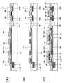
본 발명의 일양태인 고체 촬상 소자의 화소 부분의 일례를 도 1에 단면도로 나타낸다. 도 1은 전송 트랜지스터(101) 및 리셋 트랜지스터(121)에 산화물 반도체를 가지는 박막 트랜지스터를 이용한 예이고, 증폭 트랜지스터(131)는 단결정 실리콘 기판(100)에 형성된 n채널형의 벌크 트랜지스터로 형성한다. 광전 변환 소자(110)는 n형 영역(112)과 얇은 p형 영역(114)을 포함하는 포토 다이오드이고, 전송 트랜지스터(101)의 소스 전극(104)으로 접속된다. 또한, 전송 트랜지스터(101)의 드레인 전극 하방 및 리셋 트랜지스터의 소스 전극 하방에는 신호 전하 축적부(116)(플로팅 디퓨젼(floating diffusion)이라고도 함)가 형성된다. 전송 트랜지스터(101) 및 리셋 트랜지스터(121)은 산화물 반도체층이 채널 영역이 되는 탑 게이트 구조를 하고 있고, 전송 트랜지스터(101)의 드레인 전극(106)이 리셋 트랜지스터의 소스 전극(124)과 전기적으로 접속된다. 증폭 트랜지스터(131)는 n형 영역(132a, 132b)과 게이트 전극(138)을 포함하는 n채널형의 벌크 트랜지스터이고, 도시하지는 않았지만, 증폭 트랜지스터의 게이트 전극(138)은 신호 전하 축적부(116)와 전기적으로 접속된다.Fig. 1 is a cross-sectional view showing an example of a pixel portion of the solid-state image pickup device of the present invention. 1 shows an example in which a thin film transistor having an oxide semiconductor is used for the
또한, 도 1의 구조에 있어서, 벌크 트랜지스터의 게이트 절연층(136)은 박막 트랜지스터인 전송 트랜지스터(101) 및 리셋 트랜지스터(121)의 베이스 절연층을 겸하고, 신호 전하 축적부(116)는 게이트 절연층(136)을 유전체로서 용량을 형성한다. 또한, 박막 트랜지스터의 게이트 절연층(118)은 벌크 트랜지스터의 층간 절연층의 일부로서 기능한다.1, the
산화물 반도체를 채널 형성 영역에 이용한 박막 트랜지스터는 탑 게이트형을 예로서 나타내었지만, 역스태거 구조 등의 보텀 게이트형을 이용하여도 좋다. 또한, 광전 변환 소자(110)에 광을 조사할 필요가 있기 때문에, 전송 트랜지스터(101)의 소스 전극의 일부를 광전 변환 소자(110)의 수광부에 접속시키는 예를 들었지만, 소스 전극을 투광성 도전 재료로 형성하고, 광전 변환 소자(110)와의 접속 상태를 바꿔도 좋다. 예를 들어, 도 2(A)에 나타낸 바와 같이, 투광성 도전 재료로 형성한 소스 전극(204)을 가지는 트랜지스터(201)를 전송 트랜지스터로서 이용하면, 소스 전극은 광전 변환 소자(210)의 수광면의 일부 또는 전면에 접속할 수 있다. 또한, 도 2(B)에 나타낸 바와 같이 광전 변환 소자(310)로의 광로를 확보할 수 있도록, 저항이 낮은 금속층을 소스 전극(304) 및 드레인 전극(306)로 하고, 투광성 도전 재료층을 버퍼층(305, 307)으로 하여 적층한 트랜지스터(301)을 전송 트랜지스터로서 이용하여도 좋다.Though the top gate type thin film transistor using the oxide semiconductor as the channel forming region is shown as an example, a bottom gate type such as a reverse stagger structure may be used. Although it is necessary to irradiate the
광전 변환 소자으로서는, p형 단결정 실리콘 기판(SOI의 경우는 p형 단결정 실리콘층)에 n형 영역을 형성하고, 그 상부에 얇은 p형 영역을 형성한 소위 매립형 포토 다이오드를 형성한다. 포토 다이오드의 표면에 p형 영역을 형성함으로써 표면에서 발생하는 암(暗)전류, 즉 노이즈를 저감할 수 있다.As the photoelectric conversion element, a so-called buried photodiode in which an n-type region is formed in a p-type single crystal silicon substrate (p-type single crystal silicon layer in the case of SOI) and a thin p- By forming the p-type region on the surface of the photodiode, the dark current (i.e., noise) generated on the surface can be reduced.
또한, 상기에서는 단결정 반도체 기판을 이용한 예를 나타내었지만, SOI 구조의 기판이어도 좋다. 또한, 벌크 트랜지스터의 구조는 이것으로 한정되지 않고, 게이트 전극단에 사이드 월을 형성한 LDD(Lightly Doped Drain) 구조나 소스 또는 드레인 영역의 일부에 저저항의 실리사이드 등을 형성한 구조이어도 좋다.Although an example using a single crystal semiconductor substrate is shown above, it may be a substrate having an SOI structure. In addition, the structure of the bulk transistor is not limited to this, and a LDD (Lightly Doped Drain) structure in which a sidewall is formed at the gate front end or a structure in which a low-resistance silicide or the like is formed in a part of the source or drain region.
또한, 상기 화소부에는 증폭 트랜지스터(131)와 전기적으로 접속되는 선택 트랜지스터를 설치하여도 좋다. 증폭 트랜지스터 및 선택 트랜지스터는 동시에 실리콘 반도체, 산화물 반도체 중 어느 것을 이용하여도 형성할 수 있다. 단, 증폭 트랜지스터는 보다 증폭율이 높은 실리콘 반도체층을 이용한 벌크 트랜지스터로 형성하는 것이 바람직하다.A selection transistor electrically connected to the amplifying
또한, 벌크 트랜지스터의 상부에 절연층을 형성하고, 그 위에 박막 트랜지스터를 형성할 수도 있다. 예를 들어, 박막 트랜지스터에서 형성하는 전송 트랜지스터, 또는 리셋 트랜지스터 중 어느 한쪽을 벌크 트랜지스터에서 설치하는 증폭 트랜지스터의 상부에 설치하면, 한 화소 당 필요한 트랜지스터의 면적이 2/3 정도가 되고, 집적도의 향상이나 포토 다이오드의 수광 면적을 증가시킬 수 있고, 노이즈를 저감시킬 수도 있다. 도 3(A)는 그 일례이다. 박막 트랜지스터로 형성된 전송 트랜지스터(401)와 벌크 트랜지스터로 형성된 증폭 트랜지스터(431)가 병설되고, 그 상부에 절연층(441)을 통하여 박막 트랜지스터로 형성된 리셋 트랜지스터(421)가 설치된 구조를 하고 있다. 또한, 도 3(B)는, 하층에 광전 변환 소자(510)와 벌크 트랜지스터로 형성된 증폭 트랜지스터(531)를 형성하고, 절연막(541)을 통하여 상층에 박막 트랜지스터로 형성된 전송 트랜지스터(501)와 리셋 트랜지스터(521)를 설치한 예가 있고, 광전 변환 소자 및 벌크 트랜지스터와 박막 트랜지스터의 제작 공정이 분리될 수 있기 때문에, 공정의 제어가 용이하게 된다. 단, 신호 전하 축적부(516)를 형성하기 위한 용량 전극(540)을 설치해 두는 것이 바람직하다.Further, an insulating layer may be formed on the upper portion of the bulk transistor, and a thin film transistor may be formed thereon. For example, when either the transfer transistor or the reset transistor formed in the thin film transistor is provided on the upper portion of the amplification transistor provided in the bulk transistor, the area of the transistor required per pixel is about 2/3, Or the light receiving area of the photodiode can be increased, and the noise can be reduced. 3 (A) is an example thereof. A structure in which a
이상의 박막 트랜지스터와 벌크 트랜지스터를 조합시키는 구성에 의하여, 신호 전하 축적부의 전위의 보유 기능을 높이고, 다이나믹 레인지가 넓은 고체 촬상 소자의 화소부를 형성할 수 있다. 단, 본 발명의 일양태를 실현하기 위해서는 오프 전류가 매우 낮은 박막 트랜지스터를 이용하는 것이 바람직하다. 다음에 그 제작 방법을 설명한다.By combining the above-described thin-film transistor and bulk transistor, the pixel portion of the solid-state image pickup device having a wider dynamic range can be formed by enhancing the potential holding function of the signal charge storage portion. However, in order to realize an aspect of the present invention, it is preferable to use a thin film transistor having a very low off current. Next, the manufacturing method will be described.
본 발명의 일양태는, 단결정 실리콘 반도체를 이용한 벌크 트랜지스터와 전기 특성이 매우 양호한 산화물 반도체를 이용한 박막 트랜지스터를 조합시킴으로써 고체 촬상 소자의 화소부를 형성하는 것이다. 따라서, 산화물 반도체를 이용한 박막 트랜지스터의 제작 방법을 중심으로 상세하게 설명한다.One aspect of the present invention is to form a pixel portion of a solid-state image pickup device by combining a bulk transistor using a single crystal silicon semiconductor and a thin film transistor using an oxide semiconductor having a very good electric characteristic. Therefore, a method of manufacturing a thin film transistor using an oxide semiconductor will be described in detail.
일례로서, 도 1의 구조의 제작 방법을 도 4 및 도 5의 단면도를 이용하여 설명한다. 먼저, P형의 단결정 실리콘 기판(100)에 절연막(140)(필드 산화막이라고도 함)으로 분리한 소자 형성 영역을 형성한다. 소자 분리 영역의 형성은 LOCOS법(Local Oxidation Of Silicon법)이나 STI법(Shallow Trench Isolation) 등을 이용할 수 있다.As an example, a manufacturing method of the structure of FIG. 1 will be described with reference to FIGS. 4 and 5. First, an element formation region isolated by an insulating film 140 (also referred to as a field oxide film) is formed on a P-type single
여기에서 기판은 단결정 실리콘 기판으로 한정되지 않고, SOI(Silicon On Insulator) 기판 등을 이용할 수도 있다.Here, the substrate is not limited to a single crystal silicon substrate, and an SOI (Silicon On Insulator) substrate or the like may be used.
또한, 본 실시형태에서는 매립형의 포토 다이오드및 n채널형의 벌크 트랜지스터를 이용하는 구성이기 때문에, p형 단결정 실리콘 기판을 이용하지만, p웰(p-well)을 형성하면 n형 단결정 실리콘 기판을 이용할 수도 있다.In this embodiment, a p-type single crystal silicon substrate is used because a buried photodiode and an n-channel type bulk transistor are used. However, if a p-well is formed, an n-type single crystal silicon substrate may be used have.
다음에, 소자 형성 영역을 덮도록 게이트 절연층(136)을 형성한다. 예를 들어, 열처리를 행하여 단결정 실리콘 기판(100)에 형성된 소자 형성 영역의 표면을 산화시킴으로써 산화 실리콘막을 형성할 수 있다. 또한, 열산화법에 의하여 산화 실리콘막을 형성한 후에, 질화 처리를 행함으로써 산화 실리콘막의 표면을 질화시킴으로써, 산화 실리콘막과 산질화 실리콘막과의 적층 구조로 형성하여도 좋다.Next, the
다른 방법으로는 예를 들어, 단결정 실리콘 기판(100)에 형성된 소자 형성 영역의 표면에 고밀도 플라즈마 처리에 의하여 산화 처리 또는 질화 처리를 행함으로써, 게이트 절연층(136)으로서 산화 실리콘막 또는 질화 실리콘막으로 형성할 수 있다. 또한, 고밀도 플라즈마 처리에 의하여 소자 형성 영역의 표면에 산화 처리를 행한 후에, 재차 고밀도 플라즈마 처리를 행함으로써 질화 처리를 행하여도 좋다. 이 경우, 소자 형성 영역의 표면에 접하여 산화 실리콘막이 형성되고, 이 산화 실리콘막 위에 산질화 실리콘막이 형성되고, 게이트 절연층(136)은 산화 실리콘막과 산질화 실리콘막이 적층된 층이 된다.Alternatively, for example, the surface of the element formation region formed in the single
다음에, 게이트 절연층(136)을 덮도록 도전층을 형성한다. 여기에서는 도전층(138a)과 도전층(138b)을 순서대로 적층하여 형성한다. 물론, 도전층은 단층 또는 2층 이상의 적층 구조로 형성하여도 좋다.Next, a conductive layer is formed so as to cover the
도전층(138a, 138b)으로서는, 탄탈(Ta), 텅스텐(W), 티탄(Ti), 몰리브덴(Mo), 알루미늄(Al), 구리(Cu), 크롬(Cr), 니오브(Nb) 등에서 선택된 원소 또는 이것들의 원소를 주성분으로 하는 합금 재료나 화합물 재료로 형성할 수 있다. 또한, 이것들의 원소를 질화한 금속 질화막으로 형성할 수도 있다. 그 외에도, 인 등의 불순물 원소를 도핑한 다결정 실리콘으로 대표되는 반도체 재료에 의하여 형성할 수도 있다.The
여기에서는, 도전층(138a)으로서 질화 탄탈을 이용하여 형성하고, 그 위에 도전층(138b)으로서 텅스텐을 이용하여 적층 구조로 형성한다. 또한, 그 외에도 도전층(138a)으로서 질화 텅스텐, 질화 몰리브덴 또는 질화 티탄에서 선택된 단층 또는 적층막을 이용하고, 도전층(138b)으로서 탄탈, 몰리브덴, 티탄에서 선택된 단층 또는 적층막을 이용할 수 있다.
Here, tantalum nitride is used as the
*다음에, 적층하여 형성된 도전층(138a, 138b)을 선택적으로 에칭하여 제거함으로써, 게이트 절연층(136) 상방의 일부에 도전층(138a, 138b)을 잔존시켜, 게이트 전극(138)을 형성한다.Next, the
다음에, 소자 형성 영역 이외를 덮도록 레지스트 마스크를 선택적으로 형성하고, 이 레지스트 마스크 및 게이트 전극(138)을 마스크로 하여 불순물 원소를 도입함으로써 n형 영역(132a, 132b)의 불순물 영역을 형성한다. 여기에서는 n채널형의 벌크 트랜지스터를 형성하기 때문에, 불순물 원소로서는 n형을 부여하는 불순물 원소인 인(P)나 비소(As) 등을 이용할 수 있다.Next, a resist mask is selectively formed to cover the regions other than the element formation regions, and an impurity element is introduced using the resist mask and the
다음에, 광전 변환 소자인 포토 다이오드를 제작하기 위하여 레지스트 마스크를 선택적으로 형성한다. 먼저, n형을 부여하는 불순물 원소인 인(P)이나 비소(As)를 p형 단결정 실리콘 기판에 도입시켜 pn 접합을 형성한 후, p형을 부여하는 불순물 원소인 붕소(B)를 n형 영역의 표층으로 도입함으로써 매립형의 포토 다이오드를 형성할 수 있다.Next, a resist mask is selectively formed to fabricate a photodiode which is a photoelectric conversion element. First, phosphorus (P) or arsenic (As), which is an impurity element imparting n-type conductivity, is introduced into a p-type single crystal silicon substrate to form a pn junction and then boron (B) Type photodiodes can be formed by introducing them into the surface layer of the region.
이 단계에서, 도 4(A)의 우측에 나타낸 벌크 트랜지스터와 좌측에 나타낸 포토 다이오드의 구조가 완성된다.At this stage, the structure of the bulk transistor shown on the right side of Fig. 4 (A) and the photodiode shown on the left side are completed.
다음에 산화물 반도체층을 채널 영역으로 하는 박막 트랜지스터의 제작 방법에 대하여 설명한다.Next, a method of manufacturing a thin film transistor having the oxide semiconductor layer as a channel region will be described.
본 실시형태에서는 이미 단결정 실리콘 기판(100)에 형성된 벌크 트랜지스터의 게이트 절연층(136) 위에 박막 트랜지스터를 형성한다. 즉, 게이트 절연층(136)은 박막 트랜지스터의 베이스막과 벌크 트랜지스터의 게이트 절연층을 겸할 수 있다. 단, 다음의 방법을 이용하여 절연층을 성막하고, 베이스막을 적층하여도 좋다.In the present embodiment, a thin film transistor is formed on the
산화물 반도체층과 접하는 절연층으로는 산화 실리콘층, 산화 질화 실리콘층, 산화 알루미늄층 또는 산화 질화 알루미늄층 등의 산화물 절연층을 이용하는 것이 바람직하다. 절연층의 형성 방법으로서는, 플라즈마 CVD법 또는 스퍼터링법 등을 이용할 수 있지만, 절연층 중에 수소가 다량으로 포함되지 않도록 하기 위해서는, 스퍼터링법으로 절연층을 성막하는 것이 바람직하다.As the insulating layer in contact with the oxide semiconductor layer, it is preferable to use an oxide insulating layer such as a silicon oxide layer, a silicon oxynitride layer, an aluminum oxide layer or an aluminum oxynitride layer. Plasma CVD, sputtering, or the like can be used as a method of forming the insulating layer. In order to prevent a large amount of hydrogen from being contained in the insulating layer, it is preferable to form the insulating layer by the sputtering method.
절연층으로서, 스퍼터링법에 의하여 산화 실리콘층을 형성하는 예를 설명한다. 단결정 실리콘 기판(100)를 처리실로 반송하고, 수소 및 수분이 제거된 고순도 산소를 포함하는 스퍼터링 가스를 도입하여 실리콘 타겟을 이용하고, 그런 방법으로 단결정 실리콘 기판(100)에 절연층으로서 산화 실리콘층을 성막한다. 또한 단결정 실리콘 기판(100)은 실온이어도 좋고, 가열되어도 좋다.As an insulating layer, an example of forming a silicon oxide layer by a sputtering method will be described. A single
예를 들어, 석영(바람직하게는 합성 석영)을 타겟으로서 이용하고, 기판 온도 108℃, 기판과 타겟 사이의 거리(T-S 사이 거리)를 60 mm, 압력 0.4 Pa, 고주파 전원 1.5 kW 산소 및 아르곤(산소 유량 25 sccm:아르곤 유량 25 sccm=1:1)분위기 하에서 RF 스퍼터링법에 의하여 산화 실리콘층을 성막한다. 막 두께는 100 nm로 한다. 또한, 석영을 대신하여 실리콘을 산화 실리콘층을 성막하기 위한 타겟으로서 이용할 수 있다. 이 때, 스퍼터링 가스로서는 산소 또는 산소 및 아르곤의 혼합 가스를 이용하여 행한다.For example, quartz (preferably synthetic quartz) is used as a target, and the substrate temperature is 108 占 폚, the distance between the substrate and the target (distance between T and S) is 60 mm, the pressure is 0.4 Pa, A silicon oxide layer is formed by RF sputtering under an atmosphere of argon (oxygen flow rate 25 sccm: argon flow rate 25 sccm = 1: 1). The film thickness is set to 100 nm. Further, silicon can be used as a target for forming a silicon oxide layer in place of quartz. At this time, oxygen or a mixed gas of argon and oxygen is used as the sputtering gas.
이 경우에서, 처리실 내의 잔류 수분을 제거하면서 절연층을 성막하는 것이 바람직하다. 절연층에 수소, 수산기 또는 수분이 포함되지 않도록 하기 위함이다.In this case, it is preferable to form the insulating layer while removing residual moisture in the treatment chamber. So that the insulating layer does not contain hydrogen, hydroxyl or water.
처리실 내의 잔류 수분을 제거하기 위해서는, 흡착형의 진공 펌프를 이용하는 것이 바람직하다. 예를 들어, 크라이오 펌프, 이온 펌프, 티탄 서블리메이션 펌프를 이용하는 것이 바람직하다. 또한, 배기 수단으로서는, 터보 펌프에 콜드 트랩을 더한 것이어도 좋다. 크라이오 펌프를 이용하여 배기한 처리실은 예를 들어, 수소 원자나, 물(H2O) 등 수소 원자를 포함하는 화합물 등이 배기되기 때문에, 이 처리실에서 성막하여 절연층에 포함되는 불순물의 농도를 저감할 수 있다.In order to remove the residual moisture in the treatment chamber, it is preferable to use an adsorption type vacuum pump. For example, it is preferable to use a cryo pump, an ion pump, and a titanium sublimation pump. As the exhaust means, a cold trap may be added to the turbo pump. Since the treatment chamber evacuated by using the cryo pump is exhausted from, for example, a hydrogen atom or a compound containing a hydrogen atom such as water (H2 O), the concentration of the impurity contained in the insulating layer Can be reduced.
절연층을 성막할 때에 이용하는 스퍼터링 가스는 수소, 물, 수산기 또는 수소화물 등의 불순물이 ppm정도의 농도 또는 ppb정도의 농도까지 제거된 고순도 가스를 이용하는 것이 바람직하다.The sputtering gas used when depositing the insulating layer is preferably a high purity gas in which impurities such as hydrogen, water, hydroxyl, or hydride are removed to a concentration of about ppm or a concentration of about ppb.
스퍼터링법에는 스퍼터링용 전원에 고주파 전원을 이용하는 RF 스퍼터링법, DC 스퍼터링법, 또한 펄스적으로 바이어스를 주는 펄스 DC 스퍼터링법이 있다. RF 스퍼터링법은 주로 절연막을 성막하는 경우에 이용되고, DC 스퍼터링법은 주로 도전막을 성막하는 경우에 이용된다.The sputtering method includes RF sputtering using a high frequency power source as a power source for sputtering, DC sputtering, and pulse DC sputtering with a pulse bias. The RF sputtering method is mainly used for forming an insulating film, and the DC sputtering method is mainly used for forming a conductive film.
또한, 재료가 상이한 타겟을 복수 설치할 수 있는 다원 스퍼터링 장치도 있다. 다원 스퍼터링 장치는 동일 체임버에서 상이한 재료막을 적층 성막하는 것도, 동일 체임버에서 복수 종류의 재료의 막을 동시에 방전시켜 성막할 수도 있다.There is also a multi-sputtering apparatus in which a plurality of targets having different materials can be provided. The multi-sputtering apparatus may be formed by depositing a different material film in the same chamber or by simultaneously discharging a film of a plurality of kinds of materials in the same chamber.
또한, 체임버 내부에 자석 기구를 구비한 마그네트론 스퍼터링법을 이용하는 스퍼터링 장치나, 글로 방전을 사용하지 않고 마이크로파를 이용하여 발생시킨 플라즈마를 이용하는 ECR 스퍼터링을 이용하는 스퍼터링 장치가 있다.There is also a sputtering apparatus using a magnetron sputtering method having a magnet mechanism inside a chamber or a sputtering apparatus using ECR sputtering using a plasma generated by using microwaves without using a glow discharge.
또한, 스퍼터링법을 이용하는 성막 방법으로서, 성막 중에 타겟 물질과 스퍼터링 가스 성분을 서로 화학 반응시킨 그것들의 화합물 박막을 형성하는 리액티브 스퍼터링법이나, 성막 중에 기판에도 전압을 가하는 바이어스 스퍼터링법도 있다.As a film forming method using the sputtering method, a reactive sputtering method of forming a compound thin film in which a target material and a sputtering gas component are chemically reacted with each other during film formation, or a bias sputtering method of applying a voltage to a substrate during film formation.
또한, 절연층은 적층 구조이어도 좋고, 예를 들어, 기판 측으로부터 질화 실리콘층, 질화 산화 실리콘층, 질화 알루미늄층, 또는 질화 산화 알루미늄층 등의 질화물 절연층과, 상기 산화물 순서로 절연층의 적층 구조로 하여도 좋다.The insulating layer may be a laminated structure. For example, a nitride insulating layer such as a silicon nitride layer, a silicon nitride oxide layer, an aluminum nitride layer, or an aluminum nitride oxide layer may be laminated from the substrate side, Structure.
예를 들어, 산화 실리콘층과 기판의 사이에 수소 및 수분이 제거된 고순도 질소를 포함하는 스퍼터링 가스를 도입하고 실리콘 타겟을 이용하여 질화 실리콘층을 성막한다. 이 경우에서도, 산화 실리콘층과 마찬가지로, 처리실 내의 잔류 수분을 제거하면서 질화 실리콘층을 성막하는 것이 바람직하다.For example, a sputtering gas containing hydrogen and moisture-removed high-purity nitrogen is introduced between the silicon oxide layer and the substrate, and the silicon nitride layer is formed using the silicon target. Also in this case, similarly to the silicon oxide layer, it is preferable to form the silicon nitride layer while removing residual moisture in the processing chamber.
질화 실리콘층을 형성하는 경우도, 성막 시에 기판을 가열하여도 좋다.In the case of forming the silicon nitride layer, the substrate may be heated at the time of film formation.
절연층으로서 질화 실리콘층과 산화 실리콘층을 적층하는 경우, 질화 실리콘층과 산화 실리콘층을 같은 처리실에서, 공통의 실리콘 타겟을 이용하여 성막할 수 있다. 먼저 질소를 포함하는 스퍼터링 가스를 도입하고, 처리실 내에 장착된 실리콘 타겟을 이용하여 질화 실리콘층을 형성하고, 다음에 스퍼터링 가스를 산소를 포함하는 스퍼터링 가스로 변경하여 같은 실리콘 타겟을 이용하여 산화 실리콘층을 성막한다. 질화 실리콘층과 산화 실리콘층을 대기에 노출시키지 않고 연속하여 형성할 수 있기 때문에, 질화 실리콘층 표면에 수소나 수분 등의 불순물이 흡착하는 것을 방지할 수 있다.When the silicon nitride layer and the silicon oxide layer are laminated as the insulating layer, the silicon nitride layer and the silicon oxide layer can be formed in the same processing chamber using a common silicon target. First, a sputtering gas containing nitrogen is introduced, a silicon nitride layer is formed by using a silicon target mounted in the processing chamber, and then a sputtering gas containing oxygen is changed to a sputtering gas, and a silicon oxide layer . It is possible to continuously form the silicon nitride layer and the silicon oxide layer without exposing the silicon nitride layer to the atmosphere, so that impurities such as hydrogen and moisture can be prevented from being adsorbed on the surface of the silicon nitride layer.
다음으로, 절연층 위(본 실시형태에서는 게이트 절연층(136) 위)에, 막 두께 2 nm 이상 200 nm 이하의 산화물 반도체막을 스퍼터링법으로 형성한다.Next, an oxide semiconductor film having a thickness of 2 nm or more and 200 nm or less is formed on the insulating layer (on the
또한, 산화물 반도체막에 수소, 수산기 그룹 및 수분이 되도록 포함되지 않도록 하기 위하여, 성막의 전처리로서, 스퍼터링 장치의 예비 가열실에서 단결정 실리콘 기판(100)을 예비 가열하고, 이 기판에 흡착한 수소, 수분 등의 불순물을 이탈하여 배기하는 것이 바람직하다. 또한, 예비 가열실에 형성하는 배기 수단은 크라이오 펌프가 바람직하다. 또한, 이 예비 가열 처리는 생략할 수 있다. 또한, 이 예비 가열은 후에 형성하는 박막 트랜지스터의 게이트 절연층(118)의 성막 전에 행하여도 좋고, 후에 형성하는 소스 전극 및 드레인 전극이 되는 도전층의 성막 전에 행하여도 좋다.In order to prevent the oxide semiconductor film from being included in the hydrogen, hydroxyl group and moisture, the single
또한, 산화물 반도체막을 스퍼터링법에 의하여 성막하기 전에, 아르곤 가스를 도입하여 플라즈마를 발생시키는 역스퍼터링을 행하고, 절연층의 표면에 부착한 먼지를 제거하는 것이 바람직하다. 역스퍼터링이란, 아르곤 분위기 하에서 기판 측에 RF 전원을 이용하여 전압을 인가하고, 이온화한 아르곤을 기판에 충돌시켜 표면을 개질하는 방법이다. 또한, 아르곤을 대신하여 질소, 헬륨, 산소 등을 이용하여도 좋다.Before the oxide semiconductor film is formed by the sputtering method, it is preferable to carry out reverse sputtering in which argon gas is introduced to generate plasma to remove dust adhering to the surface of the insulating layer. Inverse sputtering is a method in which a voltage is applied to a substrate side in an argon atmosphere using an RF power source and ionized argon is collided with a substrate to modify the surface. In place of argon, nitrogen, helium, oxygen, or the like may be used.
산화물 반도체막은 스퍼터링법에 의하여 성막한다. 산화물 반도체막으로서는 사원계 금속 산화물인 In-Sn-Ga-Zn-O막이나, 삼원계 금속 산화물인 In-Ga-Zn-O막, In-Sn-Zn-O막, In-Al-Zn-O막, Sn-Ga-Zn-O막, Al-Ga-Zn-O막, Sn-Al-Zn-O막이나, 이원계 금속 산화물인 In-Zn-O막, Sn-Zn-O막, Al-Zn-O막, Zn-Mg-O막, Sn-Mg-O막, In-Mg-O막이나, In-O막, Sn-O막, Zn-O막 등의 산화물 반도체막을 이용할 수 있다. 또한, 상기 산화물 반도체막에 SiO2를 포함하여도 좋다.The oxide semiconductor film is formed by a sputtering method. As the oxide semiconductor film, an In-Sn-Ga-Zn-O film which is an epitaxial metal oxide, an In-Ga-Zn-O film which is a ternary metal oxide, an In- An In-Zn-O film, a Sn-Zn-O film, an Al-Ga-Zn-O film, a Sn- An oxide semiconductor film such as a -Zn-O film, a Zn-Mg-O film, a Sn-Mg-O film, an In-Mg-O film, an In-O film, a Sn-O film and a Zn- . It is also possible, including SiO2 in the oxide semiconductor film.
또한, 산화물 반도체막은 InMO3(ZnO)m(m>0)으로 표기되는 박막을 이용할 수 있다. 여기에서, M은 Ga, Al, Mn 및 Co에서 선택된 하나 또는 복수의 금속 원소를 나타낸다. 예를 들어 M으로서 Ga, Ga 와 Al, Ga 와 Mn 또는 Ga 와 Co 등이 있다. InMO3(ZnO)m(m>0)으로 표기되는 구조의 산화물 반도체막 중, M으로서 Ga를 포함하는 구조의 산화물 반도체를 In-Ga-Zn-O 산화물 반도체라고 칭하고, 그 박막을 In-Ga-Zn-O막이라고도 칭하기로 한다.The oxide semiconductor film may be a thin film denoted by InMO3 (ZnO)m (m > 0). Here, M represents one or a plurality of metal elements selected from Ga, Al, Mn and Co. For example, Ga, Ga and Al, Ga and Mn, or Ga and Co as M, for example. Among the oxide semiconductor films having a structure represented by InMO3 (ZnO)m (m > 0), an oxide semiconductor having a structure including Ga as M is referred to as an In-Ga-Zn-O oxide semiconductor, -Zn-O film.
본 실시형태에서는, 산화물 반도체막을 In-Ga-Zn-O계 금속 산화물 타겟을 이용하여 스퍼터링법에 의하여 성막한다. 또한, 산화물 반도체막은 희가스(대표적으로는 아르곤) 분위기 하, 산소 분위기 하 또는 그것들의 혼합 분위기 하에 있어서 스퍼터링법에 의하여 형성할 수 있다.In this embodiment mode, an oxide semiconductor film is formed by a sputtering method using an In-Ga-Zn-O-based metal oxide target. Further, the oxide semiconductor film can be formed by a sputtering method under an atmosphere of rare gas (typically argon) in an oxygen atmosphere or a mixed atmosphere thereof.
산화물 반도체막을 성막할 때에 이용하는 스퍼터링 가스는 수소, 물, 수산기 또는 수소화물 등의 불순물이 ppm정도의 농도 또는 ppb정도의 농도까지 제거된 고순도 가스를 이용하는 것이 바람직하다.As the sputtering gas used for forming the oxide semiconductor film, it is preferable to use a high purity gas in which impurities such as hydrogen, water, hydroxyl, or hydride are removed to a concentration of about ppm or a concentration of about ppb.
산화물 반도체막을 스퍼터링법으로 제작하기 위한 타겟으로서는 산화 아연을 주성분으로 하는 금속 산화물의 타겟을 이용할 수 있다. 예를 들어, 조성비로서, IN2O3:Ga2O3:ZnO=1:1:1[mol수비]의 금속 산화물 타겟을 이용하면 좋다. 또한, IN2O3:Ga2O3:ZnO=1:1:2[mol수비]의 금속 산화물 타겟을 이용하여도 좋다. 금속 산화물 타겟의 충진율은 90% 이상 100% 이하, 바람직하게는 95% 이상 99.9% 이하이다. 충진율이 높은 금속 산화물 타겟을 이용함으로써, 성막한 산화물 반도체막은 치밀한 막이 된다.As a target for forming an oxide semiconductor film by a sputtering method, a metal oxide target containing zinc oxide as a main component can be used. For example, a metal oxide target of IN2 O3 : Ga2 O3 : ZnO = 1: 1: 1 [molar ratio] may be used as a composition ratio. A metal oxide target of IN2 O3 : Ga2 O3 : ZnO = 1: 1: 2 [molar ratio] may also be used. The filling rate of the metal oxide target is 90% or more and 100% or less, preferably 95% or more and 99.9% or less. By using the metal oxide target having a high filling rate, the deposited oxide semiconductor film becomes a dense film.
산화물 반도체막은 감압 상태로 보유된 처리실 내에 기판을 보유하고, 처리실 내의 잔류 수분을 제거하면서 수소 및 수분이 제거된 스퍼터링 가스를 도입하고, 금속 산화물을 타겟으로 하여 절연층 위에 산화물 반도체막을 성막한다. 처리실 내의 잔류 수분을 제거하기 위해서는 흡착형의 진공 펌프를 이용하는 것이 바람직하다. 예를 들어, 크라이오 펌프, 이온 펌프, 티탄 서블리메이션 펌프를 이용하는 것이 바람직하다. 또한, 배기 수단으로서는 터보 펌프에 콜드 트랩을 더한 것이어도 좋다. 크라이오 펌프를 이용하여 배기한 처리실은 예를 들어, 수소 원자, 물(H2O) 등 수소 원자를 포함하는 화합물(보다 바람직하게는 탄소 원자를 포함하는 화합물도) 등이 배기되기 때문에, 이 처리실에서 성막한 산화물 반도체막에 포함되는 불순물의 농도를 저감할 수 있다. 또한, 산화물 반도체막 성막 시에 기판을 가열하여도 좋다.The oxide semiconductor film holds a substrate in a processing chamber held in a reduced pressure state, introduces sputtering gas from which hydrogen and moisture have been removed while removing residual moisture in the processing chamber, and forms an oxide semiconductor film on the insulating layer with the metal oxide as a target. In order to remove the residual moisture in the treatment chamber, it is preferable to use an adsorption type vacuum pump. For example, it is preferable to use a cryo pump, an ion pump, and a titanium sublimation pump. As the exhaust means, a cold trap may be added to the turbo pump. Since the treatment chamber evacuated by using the cryo pump is evacuated, for example, a hydrogen atom, a compound containing a hydrogen atom such as water (H2 O) (more preferably a compound containing a carbon atom) The concentration of the impurity contained in the oxide semiconductor film formed in the treatment chamber can be reduced. Further, the substrate may be heated at the time of forming the oxide semiconductor film.
성막 조건의 일례로서는, 기판 온도는 실온으로 기판과 타겟 사이의 거리를 110 mm, 압력 0.4 Pa, 직류(DC) 전원 0.5 kW, 산소 및 아르곤(산소 유량 15 sccm:아르곤 유량 30 sccm) 분위기 하의 조건이 적용된다. 또한, 펄스 직류(DC) 전원을 이용하면, 성막 시에 발생하는 분상 물질(파티클, 먼지라고도 함)이 경감되고, 막 두께 분포도 균일하게 되기 때문에 바람직하다. 산화물 반도체막은 바람직하게는 5 nm 이상 30 nm 이하로 한다. 또한, 산화물 반도체막의 적절한 두께는 재료에 따라 상이하고, 재료에 따라서 적절히 두께를 선택하면 좋다.As an example of the film forming conditions, the substrate temperature was set to room temperature under conditions of a distance of 110 mm between the substrate and the target, a pressure of 0.4 Pa, a direct current (DC) power of 0.5 kW, oxygen and argon (
다음으로, 산화물 반도체막을 제 1 포토리소그래피 공정 및 에칭 공정에 의하여 섬 형상의 산화물 반도체층(102, 122)으로 가공한다(도 4(B) 참조). 여기에서, 산화물 반도체층(102)은 제 1 박막 트랜지스터의 채널 영역을 형성하는 반도체층이고, 산화물 반도체층(122)은 제 2 박막 트랜지스터의 채널 영역을 형성하는 반도체층이다.Next, the oxide semiconductor film is processed into island-shaped oxide semiconductor layers 102 and 122 by a first photolithography process and an etching process (see Fig. 4 (B)). Here, the
또한, 섬 형상의 산화물 반도체층을 형성하기 위하여 이용된 레지스트 마스크는 잉크젯법으로 형성하여도 좋다. 잉크젯법에서는 포토 마스크를 사용하지 않기 때문에, 제조 원가를 저감할 수 있다. 또한, 여기에서의 산화물 반도체막의 에칭은 건식 에칭이어도 습식 에칭이어도 좋고, 둘 다 이용하여도 좋다.The resist mask used for forming the island-shaped oxide semiconductor layer may be formed by an ink-jet method. In the ink-jet method, since the photomask is not used, the manufacturing cost can be reduced. Here, the etching of the oxide semiconductor film may be dry etching, wet etching, or both.
건식 에칭에 이용하는 에칭 가스로서는, 염소를 포함하는 가스(염소계 가스, 예를 들어 염소(Cl2), 염화 붕소(BCl3), 염화 규소(SiCl4), 사염화탄소(CCl4) 등)가 바람직하다.As the etching gas used for dry etching, a gas containing chlorine (chlorine-based gas such as chlorine (Cl2 ), boron chloride (BCl3 ), silicon chloride (SiCl4 ), carbon tetrachloride (CCl4 ) .
또한, 불소를 포함하는 가스(불소계 가스, 예를 들어 사불화 탄소(CF4), 육불화 유황(SF6), 삼불화 질소(NF3), 트리플루오로메탄(CHF3) 등), 브롬화 수소(HBr), 산소(O2), 이것들의 가스에 헬륨(He)이나 아르곤(Ar) 등의 희가스를 첨가한 가스 등을 이용할 수 있다.(Fluorine-based gas such as carbon tetrafluoride (CF4 ), hexafluorosulfide (SF6 ), nitrogen trifluoride (NF3 ), trifluoromethane (CHF3 ), etc.) Hydrogen (HBr), oxygen (O2 ), a gas obtained by adding a rare gas such as helium (He) or argon (Ar) to these gases, or the like can be used.
건식 에칭법으로서는, 평행 평판형 RIE(Reactive Ion Etching)법이나, ICP(Inductively Coupled Plasma:유도 결합형 플라즈마) 에칭법을 이용할 수 있다. 소망의 가공 형상으로 에칭될 수 있도록, 에칭 조건(코일형의 전극에 인가되는 전력량, 기판 측의 전극에 인가되는 전력량, 기판 측의 전극 온도 등)을 적절히 조절한다.As the dry etching method, parallel plate type RIE (Reactive Ion Etching) method or ICP (Inductively Coupled Plasma) etching method can be used. (The amount of electric power applied to the coil-shaped electrode, the amount of electric power applied to the electrode on the substrate side, the electrode temperature on the substrate side, and the like) are appropriately controlled so as to be etched into a desired processed shape.
습식 에칭에 이용하는 에칭액으로서는, 인산과 초산과 질산을 섞은 용액, 암모니아 과수 혼합액(31 중량 % 과산화 수소수:28 중량 % 암모니아수:물=5:2:2) 등을 이용할 수 있다. 또한, ITO-07N(KANTO CHEMICAL CO.,INC 제작)을 이용하여도 좋다.As the etching solution used for the wet etching, a solution in which phosphoric acid is mixed with acetic acid and nitric acid, a mixed solution of ammonia water (31 wt% hydrogen peroxide: 28 wt% ammonia water: water = 5: 2: 2) and the like can be used. ITO-07N (manufactured by KANTO CHEMICAL CO. INC.) May also be used.
또한, 습식 에칭 후의 에칭액은 에칭된 재료와 함께 세정에 의하여 제거된다. 그 제거된 재료를 포함하는 에칭액의 폐액을 정제하고, 포함되는 재료를 재이용하여도 좋다. 이 에칭 후의 폐액에서 산화물 반도체층에 포함되는 인듐 등의 재료를 회수하여 재이용함으로써, 자원을 유효 활용하여 원가를 저감할 수 있다.Further, the etchant after the wet etching is removed by cleaning together with the etched material. The waste liquid of the etchant containing the removed material may be refined and the contained material may be reused. The material such as indium contained in the oxide semiconductor layer in the waste solution after the etching is recovered and reused, so that the resources can be effectively utilized and the cost can be reduced.
소망의 형상으로 에칭할 수 있도록, 재료에 맞추어 에칭 조건(에칭액, 에칭 시간, 온도 등)을 적절히 조절한다.The etching conditions (etching solution, etching time, temperature, and the like) are appropriately adjusted according to the material so that the desired shape can be etched.
본 실시형태에서는, 에칭액으로서 인산과 초산과 질산을 섞은 용액을 이용한 습식 에칭법에 의하여, 산화물 반도체막을 섬 형상의 산화물 반도체층(102, 122)으로 가공한다.In this embodiment, the oxide semiconductor film is processed into the island-shaped oxide semiconductor layers 102 and 122 by a wet etching method using a solution in which phosphoric acid, acetic acid and nitric acid are mixed as an etching solution.
본 실시형태에서는 산화물 반도체층(102, 122)에 대하여 질소 또는 헬륨, 네온, 아르곤 등의 희가스 분위기 하에서 제 1 가열 처리를 행한다. 제 1 가열 처리의 온도는 400℃ 이상 750℃ 이하, 바람직하게는 400℃ 이상 기판의 변형점 미만으로 한다. 여기에서는 가열 처리 장치 중 하나인 전기로에 기판을 도입하고, 산화물 반도체층에 대하여 질소 분위기 하 450℃에서 1시간의 가열 처리를 행한다. 가열 처리 온도로부터의 강온(降溫)일 때에는, 분위기를 산소로 대신하여도 좋다. 이 제 1 가열 처리에 의하여 산화물 반도체층(102, 122)의 탈수화 또는 탈수소화를 행할 수 있다.In the present embodiment, the first heat treatment is performed on the oxide semiconductor layers 102 and 122 in a rare gas atmosphere such as nitrogen or helium, neon, or argon. The temperature of the first heat treatment is set to 400 ° C or more and 750 ° C or less, preferably 400 ° C or more, and less than the strain point of the substrate. Here, a substrate is introduced into an electric furnace, which is one of the heat treatment apparatuses, and the oxide semiconductor layer is subjected to a heat treatment at 450 DEG C for 1 hour in a nitrogen atmosphere. When the temperature is lowered from the heat treatment temperature, the atmosphere may be replaced by oxygen. By this first heat treatment, the oxide semiconductor layers 102 and 122 can be dehydrated or dehydrogenated.
또한, 가열 처리 장치는 전기로에 한정되지 않고, 저항 발열체 등의 발열체로부터의 열전도 또는 열복사에 의하여, 피처리물을 가열하는 장치를 구비하여도 좋다. 예를 들어, GRTA(Gas Rapid Thermal Annealing) 장치, LRTA(Lamp Rapid Thermal Annealing) 장치 등의 RTA(Rapid Thermal Annealing) 장치를 이용할 수 있다. LRTA 장치는 할로겐 램프, 메탈핼라이드 램프, 크세논 아크 램프, 카본 아크 램프, 고압 나트륨 램프, 고압 수은 램프 등의 램프로부터 발하는 광(전자파)의 복사에 의하여, 피처리물을 가열하는 장치이다. GRTA 장치는 고온의 가스를 이용하여 가열 처리를 행하는 장치이다. 기체에는 아르곤 등의 희가스 또는 질소와 같이 가열 처리에 의하여 피처리물과 반응하지 않는 불활성 기체가 이용된다.Further, the heat treatment apparatus is not limited to the electric furnace, but may be provided with a device for heating the object to be treated by thermal conduction or heat radiation from a heating element such as a resistance heating element. For example, an RTA (Rapid Thermal Annealing) device such as a GRTA (Gas Rapid Thermal Annealing) device or an LRTA (Lamp Rapid Thermal Annealing) device can be used. The LRTA apparatus is an apparatus for heating an object to be processed by radiating light (electromagnetic waves) emitted from a lamp such as a halogen lamp, a metal halide lamp, a xenon arc lamp, a carbon arc lamp, a high pressure sodium lamp or a high pressure mercury lamp. The GRTA apparatus is a device that performs a heating process using a high-temperature gas. An inert gas such as rare gas such as argon or nitrogen which does not react with the object to be treated by heat treatment is used for the gas.
예를 들어, 제 1 가열 처리로서, 650℃ 이상 700℃ 이하의 고온으로 가열한 불활성 가스 중에 기판을 넣고, 수 분간 가열한 후에 기판 불활성 가스 중에서부터 꺼내는 GRTA를 행하여도 좋다. GRTA를 이용하면 단시간에서의 고온 가열 처리가 가능하게 된다.For example, as the first heat treatment, GRTA may be performed in which the substrate is placed in an inert gas heated to a high temperature of 650 ° C to 700 ° C, heated for several minutes, and then taken out from the substrate inert gas. The use of GRTA enables high-temperature heating treatment in a short time.
또한, 제 1 가열 처리에서는 질소, 헬륨, 네온 또는 아르곤 등의 분위기 가스에 물, 수소 등이 포함되지 않은 것이 바람직하다. 또는, 이 분위기 가스의 순도를 6 N(99.9999%) 이상, 바람직하게는 7 N(99.99999%) 이상, (즉 불순물 농도를 1ppm 이하, 바람직하게는 0.1ppm 이하)으로 한다. 분위기 가스로서 산소를 이용하는 경우도 동일한 순도인 것이 바람직하다.In the first heat treatment, it is preferable that atmospheric gas such as nitrogen, helium, neon or argon does not contain water, hydrogen or the like. Alternatively, the purity of the atmosphere gas is set to 6 N (99.9999%) or more, preferably 7 N (99.99999%) or more (that is, the impurity concentration is 1 ppm or less, preferably 0.1 ppm or less). When oxygen is used as the atmospheric gas, the same purity is also preferable.
또한, 제 1 가열 처리의 조건 또는 산화물 반도체층의 재료에 따라서는 산화물 반도체층이 결정화하고, 미결정층 또는 다결정층이 되는 경우도 있다. 예를 들어, 결정화율이 90% 이상 또는 80% 이상의 미결정의 산화물 반도체층이 되는 경우도 있다. 또한, 제 1 가열 처리의 조건 또는 산화물 반도체층의 재료에 따라서는 결정 성분을 포함하지 않은 비정질의 산화물 반도체층이 되는 경우도 있다. 또한, 비정질의 산화물 반도체층의 중에 미결정부(입경 1 nm 이상 20 nm 이하(대표적으로는 2 nm 이상 4 nm 이하))가 혼재하는 산화물 반도체층이 되는 경우도 있다.Depending on the conditions of the first heat treatment or the material of the oxide semiconductor layer, the oxide semiconductor layer may be crystallized to become a microcrystalline layer or a polycrystalline layer. For example, the crystallization rate may be 90% or more or 80% or more of a microcrystalline oxide semiconductor layer. Depending on the conditions of the first heat treatment or the material of the oxide semiconductor layer, there may be an amorphous oxide semiconductor layer not containing a crystal component. In some cases, an oxide semiconductor layer in which amorphous oxide semiconductor layer has a crystal grain size (1 nm or more and 20 nm or less (typically 2 nm or more and 4 nm or less)) may be mixed.
또한, 산화물 반도체층의 제 1 가열 처리는 섬 형상의 산화물 반도체층에 가공하기 전의 산화물 반도체막에 행할 수도 있다.Further, the first heat treatment of the oxide semiconductor layer may be performed on the oxide semiconductor film before being processed into the island-shaped oxide semiconductor layer.
산화물 반도체층에 대한 탈수화, 탈수소화의 효과를 얻는 가열 처리는 산화물 반도체층 성막 후, 산화물 반도체층 위에 소스 전극 및 드레인 전극을 적층시킨 후, 소스 전극 및 드레인 전극 위에 게이트 절연층을 형성한 후, 둘 중 어느 것을 행하여도 좋다.In the heat treatment for obtaining the effect of dehydration and dehydrogenation of the oxide semiconductor layer, after forming the oxide semiconductor layer, a source electrode and a drain electrode are laminated on the oxide semiconductor layer, and then a gate insulating layer is formed on the source electrode and the drain electrode , Or either of them may be performed.
다음으로, 제 2 포토리소그래피 공정 및 에칭 공정에 의하여 포토 다이오드 상층의 P+층에 달하는 개구부를 절연층에 형성하고, 절연층 및 산화물 반도체층(102, 122) 위에 도전층을 형성한다. 도전층을 스퍼터링법이나 진공 증착법으로 형성하면 좋다. 도전층의 재료로서는 알루미늄, 크롬, 구리, 탄탈, 티탄, 몰리브덴, 텅스텐에서 선택된 원소 또는 상기 원소를 성분으로 하는 합금이나, 상기한 원소를 조합한 합금막 등을 들 수 있다. 또한, 망간, 마그네슘, 지르코늄, 베릴륨, 이트륨 중 어느 하나 또는 복수에서 선택된 재료를 이용하여도 좋다. 또한, 금속 도전층은 단층 구조이어도 좋고, 2층 이상의 적층 구조로 하여도 좋다. 예를 들어, 실리콘을 포함하는 알루미늄막의 단층 구조, 알루미늄막 위에 티탄막을 적층하는 2층 구조, 티탄막과, 그 티탄막 위에 겹쳐서 알루미늄막을 적층하고, 그 위에 티탄막을 더 성막하는 3층 구조 등을 들 수 있다. 또한, 알루미늄에 티탄, 탄탈, 텅스텐, 몰리브덴, 크롬, 네오듐, 스칸듐에서 선택된 원소를 단수 또는 복수 조합한 막, 합금막, 또는 질화막을 이용하여도 좋다.Next, an opening reaching the P+ layer of the upper layer of the photodiode is formed in the insulating layer by a second photolithography process and an etching process, and a conductive layer is formed on the insulating layer and the oxide semiconductor layers 102 and 122. The conductive layer may be formed by a sputtering method or a vacuum deposition method. As the material of the conductive layer, an element selected from the group consisting of aluminum, chromium, copper, tantalum, titanium, molybdenum and tungsten, an alloy containing the above element, and an alloy film obtained by combining these elements can be given. Further, a material selected from any one or more of manganese, magnesium, zirconium, beryllium, and yttrium may be used. The metal conductive layer may have a single-layer structure or a laminated structure of two or more layers. For example, a three-layer structure in which a single layer structure of an aluminum film containing silicon, a two-layer structure of a titanium film laminated on an aluminum film, a titanium film, an aluminum film superimposed on the titanium film, . Further, a film, an alloy film, or a nitride film in which a single element or a plurality of elements selected from titanium, tantalum, tungsten, molybdenum, chromium, neodymium, and scandium are combined with aluminum may be used.
다음에, 제 3 포토리소그래피 공정에서 도전층 위에 레지스트 마스크를 형성하고, 선택적으로 에칭을 행하여, 제 1 박막 트랜지스터의 소스 전극(104) 및 드레인 전극(106), 제 2 박막 트랜지스터의 소스 전극(124) 및 드레인 전극(126)을 형성한 후, 레지스트 마스크를 제거한다(도 4(C) 참조). 여기에서, 제 1 박막 트랜지스터의 드레인 전극(106)과 제 2 박막 트랜지스터의 소스 전극(124)은 전기적으로 접속된 상태로 형성되지만 절연된 상태여도 좋고, 후에 배선을 이용하여 전기적으로 접속하여도 좋다. 또한, 형성된 소스 전극, 드레인 전극의 단부가 테이퍼라면, 위에 적층하는 게이트 절연층의 피복성이 향상되기 때문에 바람직하다.Then, a resist mask is formed on the conductive layer in the third photolithography process and selectively etched to form the
본 실시형태에서는 소스 전극(104, 124), 드레인 전극(106, 126)으로서, 스퍼터링법에 의하여 막 두께 150 nm의 티탄막을 형성한다.In this embodiment, as the
또한, 도전층의 에칭 시에, 산화물 반도체층(102, 122)은 산화물 반도체층의 일부가 제거되지 않고, 그 아래의 절연층이 노출하지 않도록 각각의 재료 및 에칭 조건을 적절히 조절한다.Further, at the time of etching the conductive layer, the oxide semiconductor layers 102 and 122 appropriately adjust the respective materials and the etching conditions so that a part of the oxide semiconductor layer is not removed and the insulating layer below it is not exposed.
본 실시형태에서는 도전층으로서 티탄막을 이용하고, 산화물 반도체층(102, 122)에는 In-Ga-Zn-O계 산화물 반도체를 이용하고, 암모니아 과수 혼합액(암모니아, 물, 과산화 수소수의 혼합액)을 이용한다.In this embodiment, an In-Ga-Zn-O-based oxide semiconductor is used for the oxide semiconductor layers 102 and 122 and a mixed solution of ammonia water and water .
또한, 제 3 포토리소그래피 공정 및 에칭 공정으로는 산화물 반도체층(102, 122)은 일부만이 에칭되고, 홈부(오목부)를 가지는 산화물 반도체층이 되는 것도 있다. 또한, 소스 전극(104, 124), 드레인 전극(106, 126)을 형성하기 위하여 레지스트 마스크를 잉크젯법으로 형성하여도 좋다. 잉크젯법은 포토 마스크를 사용하지 않기 때문에, 제조 원가를 저감할 수 있다.In the third photolithography process and the etching process, only a part of the oxide semiconductor layers 102 and 122 is etched to be an oxide semiconductor layer having a trench (recess). In order to form the
제 3 포토리소그래피 공정에서의 레지스트 마스크 형성 시의 노광에는 적외선이나 KrF 레이저광이나 ArF 레이저광을 이용한다. 산화물 반도체층(102, 122) 위에서 서로 인접하는 소스 전극의 하단부와 드레인 전극의 하단부의 간격 폭에 의하여 후에 형성되는 박막 트랜지스터의 채널 길이(L)가 결정된다. 또한, 채널 길이(L)=25 nm 미만의 노광을 행하는 경우에는, 수 nm∼수 10 nm와 파장이 매우 짧은 초적외선(Extreme Ultraviolet)을 이용하여 제 2 포토리소그래피 공정에서의 레지스트 마스크 형성 시의 노광을 행한다. 초적외선에 의하여 노광은 해상도가 높고 초점 심도도 크다. 따라서, 후에 형성되는 박막 트랜지스터의 채널 길이(L)를 10 nm 이상 1000 nm 이하로 하는 것도 가능하고, 회로의 동작 속도를 고속화할 수 있고 또한, 오프 전류값이 매우 작기 때문에, 저소비 전력화도 도모할 수 있다.Infrared rays, KrF laser light, or ArF laser light are used for exposure in forming the resist mask in the third photolithography step. The channel length L of the thin film transistor to be formed later is determined by the gap width between the lower end of the source electrode and the lower end of the drain electrode adjacent to each other on the oxide semiconductor layers 102 and 122. In the case of performing exposure with a channel length L of less than 25 nm, it is preferable to use a resist film having a thickness of several nm to several tens nm and a very short wavelength (Extreme Ultraviolet) for forming a resist mask in the second photolithography process Exposure is performed. The ultraviolet ray exposure has a high resolution and a large depth of focus. Therefore, the channel length L of the thin film transistor to be formed later can be set to 10 nm or more and 1000 nm or less, the operation speed of the circuit can be increased, and the off current value is very small. .
다음으로, 절연층, 산화물 반도체층(102, 122), 소스 전극(104, 124), 드레인 전극(106, 126) 위에 게이트 절연층(118)을 형성한다(도 5(A) 참조). 이 때, 벌크 트랜지스터 위에도 게이트 절연층(118)은 성막되고, 층간 절연막의 일부가 된다.
Next, a
*여기에서, 불순물을 제거함으로써 i형화 또는 실질적으로 i형화된 산화물 반도체(고순도화된 산화물 반도체)는 계면 준위, 계면 전하에 대하여 매우 민감하기 때문에, 게이트 절연층과의 계면은 중요하다. 그 때문에 고순도화된 산화물 반도체에 접하는 게이트 절연층(GI)은 고품질화가 요구된다.Here, the interface with the gate insulating layer is important because an oxide semiconductor (highly purified oxide semiconductor) that is i-type or substantially i-shaped by removing impurities is very sensitive to interface levels and interface charges. Therefore, the quality of the gate insulating layer (GI) in contact with the high-purity oxide semiconductor is required to be high.
예를 들어, 마이크로파(2.45 GHz)를 이용한 고밀도 플라즈마 CVD는 치밀하고 절연 내압이 높은 고품질의 절연층을 형성할 수 있으므로 바람직하다. 고순도화된 산화물 반도체와 고품질 게이트 절연층이 밀접함으로써, 계면 준위를 저감하여 계면 특성을 양호한 것으로 할 수 있다. 물론, 게이트 절연층으로서 양질의 절연층을 형성할 수 있는 것이라면, 스퍼터링법이나 플라즈마 CVD법 등 외의 성막 방법을 적용할 수 있다. 또한, 성막 후의 열처리에 의하여 게이트 절연층의 막질, 산화물 반도체와의 계면 특성이 개질되는 절연층이어도 좋다. 어느 것으로 하여도, 게이트 절연층으로서의 막질이 양호한 것은 물론, 산화물 반도체와의 계면 준위 밀도를 저감하고, 양호한 계면을 형성할 수 있는 것이면 좋다.For example, high-density plasma CVD using microwaves (2.45 GHz) is preferable because it can form a high-quality insulating layer with high density and high withstand voltage. Since the high-purity oxide semiconductor and the high-quality gate insulating layer are in close contact with each other, the interfacial level can be reduced and the interface characteristics can be improved. Of course, any film forming method other than the sputtering method, the plasma CVD method, or the like can be applied as long as a good quality insulating layer can be formed as the gate insulating layer. An insulating layer may be used in which the film quality of the gate insulating layer and the interface characteristics with the oxide semiconductor are modified by heat treatment after film formation. Any film may be used as long as it has a good film quality as the gate insulating layer and can reduce the interface level density with the oxide semiconductor and form a good interface.
또한, 85℃, 2×10⁶V/cm, 12시간의 바이어스·열 스트레스 시험(BT 시험)에서는 불순물이 산화물 반도체에 첨가되어 있으면, 불순물과 산화물 반도체의 주성분과의 결합이, 강전계(B:바이어스)와 고온(T:온도)에 의하여 절단되고, 생성된 미결합수가 스레숄드 전압(Vth)의 시프트를 유발하게 된다. 이것에 대하여, 본 발명의 일양태는 산화물 반도체의 불순물, 특히 수소나 물 등을 극력 제거하고, 상기와 같이 게이트 절연층과의 계면 특성을 양호하게 함으로써, BT 시험을 행하여도 안정된 박막 트랜지스터를 얻는 것을 가능하게 한다.If impurities are added to the oxide semiconductor in the bias and thermal stress test (BT test) at 85 占 폚 and 2 占06 V / cm for 12 hours, the bond between the impurity and the main component of the oxide semiconductor becomes stronger : Bias) and a high temperature (T: temperature), and the generated unbonded number causes a shift of the threshold voltage Vth. On the other hand, one aspect of the present invention is to obtain a stable thin film transistor even when the BT test is performed by removing the impurities of the oxide semiconductor, particularly hydrogen or water, as much as possible and improving the interface characteristics with the gate insulating layer as described above Lt; / RTI >
본 실시형태에 있어서, 게이트 절연층(118)의 형성은 마이크로파(2.45GHz)를 이용한 고밀도 플라즈마 CVD 장치에 의하여 행한다. 여기에서는, 고밀도 플라즈마 CVD 장치는 1×10¹¹/cm3 이상의 플라즈마 밀도를 달성할 수 있는 장치를 가리킨다. 예를 들어, 3 kW 이상 6 kW 이하의 마이크로파 전력을 인가하여 플라즈마를 발생시켜 절연층의 성막을 행한다.In this embodiment, the
체임버에 재료 가스로서 모노실란 가스(SiH4)와 아산화 질소(N2O)와 희가스를 도입하고, 10 Pa∼30 Pa의 압력 하에서 고밀도 플라즈마를 발생시켜 기판 위에 절연층을 형성한다. 그 후, 모노실란 가스의 공급을 정지하고, 대기에 노출되지 않고 아산화 질소(N2O)와 희가스를 도입하여 절연층 표면에 플라즈마 처리를 행하여도 좋다. 적어도 아산화 질소(N2O)와 희가스를 도입하여 절연층 표면에 행하는 플라즈마 처리는 절연층의 성막보다 후에 행한다. 상기 프로세스를 거친 절연층은 막 두께가 얇고, 예를 들어 100 nm 미만이어도 신뢰성을 확보할 수 있다.Monosilane gas (SiH4 ), nitrous oxide (N2 O) and rare gas are introduced into the chamber as a material gas, and a high-density plasma is generated under a pressure of 10 Pa to 30 Pa to form an insulating layer on the substrate. Thereafter, the supply of the monosilane gas may be stopped, and nitrous oxide (N2 O) and a rare gas may be introduced into the insulating layer without being exposed to the atmosphere to perform the plasma treatment on the surface of the insulating layer. At least the nitrous oxide (N2 O) and the rare gas are introduced to perform the plasma treatment on the surface of the insulating layer after the formation of the insulating layer. The insulating layer that has been subjected to the above process can have reliability even when the film thickness is thin, for example, less than 100 nm.
게이트 절연층(118)의 형성 시, 체임버에 도입하는 모노실란 가스(SiH4)와 아산화 질소(N2O)의 유량비는 1:10에서 1:200의 범위로 한다. 또한, 체임버에 도입하는 희가스로서는 헬륨, 아르곤, 크립톤, 크세논 등을 이용할 수 있지만, 그 중에서도 저렴한 아르곤을 이용하는 것이 바람직하다.The flow rate ratio of the monosilane gas (SiH4 ) and the nitrous oxide (N2 O) introduced into the chamber in the formation of the
또한, 고밀도 플라즈마 CVD 장치에 의하여 얻어지는 절연층은 단차 피복성이 우수하고, 막 두께를 정확하게 제어할 수 있다.In addition, the insulating layer obtained by the high-density plasma CVD apparatus is excellent in step coverage, and the film thickness can be accurately controlled.
상기 프로세스를 거친 절연층은 종래의 평행 평판형의 PECVD 장치에서 얻어지는 절연층과는 막질이 크게 상이하고, 같은 에천트를 이용한 에칭 속도에 비교하여, 평행 평판형의 PECVD 장치에서 얻어지는 절연층의 10% 이상 또는 20% 이상 에칭 속도가 늦고, 고밀도 플라즈마 CVD 장치에서 얻어지는 절연층은 치밀한 층이라고 할 수 있다.The insulating layer that has undergone the above process is significantly different in film quality from the insulating layer obtained in the conventional parallel plate type PECVD apparatus, and the etching rate of the insulating layer obtained in the parallel plate type PECVD apparatus % Or more than 20%, and the insulating layer obtained by the high-density plasma CVD apparatus is a dense layer.
본 실시형태에서는 게이트 절연층(118)으로서 고밀도 플라즈마 CVD 장치에 의하여 막 두께 100 nm의 산화 질화 규소층(SiOxNy라고도 함, 단, x>y>0)을 이용한다.In the present embodiment (also referred to as SiOxNy, stage, x>y> 0), the
그 외의 방법으로서, 게이트 절연층(118)은 플라즈마 CVD법 또는 스퍼터링법 등을 이용하여 산화 실리콘층, 질화 실리콘층, 산화 질화 실리콘층, 질화 산화 실리콘층 또는 산화 알루미늄층을 단층으로 또는 적층하여 형성할 수 있다. 또한, 게이트 절연층(118) 중에 수소가 다량으로 포함되지 않도록 하기 위해서는 스퍼터링법으로 게이트 절연층(118)을 성막하는 것도 바람직하다. 스퍼터링법에 의하여 산화 실리콘층을 성막하는 경우에는 타겟으로서 실리콘 또는 석영을 이용하고, 스퍼터링 가스로서 산소 또는 산소 및 아르곤의 혼합 가스를 이용하여 행한다.As another method, the
게이트 절연층(118)은 소스 전극(104, 124) 및 드레인 전극(106, 126) 측으로 부터 산화 실리콘층과 질화 실리콘층을 적층한 구조로 할 수도 있다. 예를 들어, 제 1 게이트 절연층으로서 막 두께 5 nm 이상 300 nm 이하의 산화 실리콘층(SiOx(x>0))을 형성하고, 제 1 게이트 절연층 상에 제 2 게이트 절연층으로서 스퍼터링법에 의하여 막 두께 50 nm 이상 200 nm 이하의 질화 실리콘층(SiNy(y>0))을 적층하고, 막 두께 100 nm의 게이트 절연층으로 하여도 좋다.The
다음으로, 제 4 포토리소그래피 공정에 의하여 레지스트 마스크를 형성하고, 선택적으로 에칭을 행하여 게이트 절연층(118)의 일부를 제거하고, 박막 트랜지스터의 드레인 전극(126) 및 벌크 트랜지스터의 소스 영역 또는 드레인 영역이 되는 n형 영역(132a, 132b)에 달하는 개구부를 형성한다(도 5(B) 참조).Next, a resist mask is formed by a fourth photolithography process, and etching is selectively performed to remove a part of the
다음에, 개구부가 형성된 게이트 절연층(118) 위에 도전층을 형성한 후, 제 5 포토리소그래피 공정 및 에칭 공정에 의하여 게이트 전극(108, 128) 및 배선층(151, 152, 153)을 형성한다. 또한, 레지스트 마스크를 잉크젯법으로 형성하여도 좋다. 잉크젯법은 포토 마스크를 사용하지 않기 때문에, 제조 원가를 저감할 수 있다.Next, after the conductive layer is formed on the
또한, 게이트 전극(108, 128) 및 배선층(151, 152, 153)은 몰리브덴, 티탄, 크롬, 탄탈, 텅스텐, 알루미늄, 구리, 네오듐, 스칸듐 등의 금속 재료 또는 이것들을 주성분으로 하는 합금 재료를 이용하여, 단층 또는 적층하여 형성할 수 있다.The
예를 들어, 게이트 전극(108, 128) 및 배선층(151, 152, 153)을 2층으로 하는 적층 구조로서는, 알루미늄층 위에 몰리브덴층이 적층된 2층의 적층 구조 또는 구리층 위에 몰리브덴층을 적층한 2층 구조 또는 구리층 위에 질화 티탄층 또는 질화 탄탈을 적층한 2층 구조, 질화 티탄층과 몰리브덴층을 적층한 2층 구조로 하는 것이 바람직하다. 3층의 적층 구조로서는 텅스텐층 또는 질화 텅스텐층과, 알루미늄과 실리콘의 합금 또는 알루미늄과 티탄의 합금과, 질화 티탄층 또는 티탄층을 적층한 적층으로 하는 것이 바람직하다. 또한, 투광성을 가지는 도전층을 이용하여 게이트 전극을 형성할 수도 있다. 투광성을 가지는 도전층으로서는 투광성 도전성 산화물 등을 그 재료의 예로 들 수 있다.For example, as the lamination structure in which the
본 실시형태에서는 게이트 전극(108, 128) 및 배선층(151, 152, 153)으로서 막 두께 150 nm의 티탄막을 스퍼터링법에 의하여 형성한다.In this embodiment, a titanium film with a thickness of 150 nm is formed as the
다음으로, 불활성 가스 분위기 하 또는 산소 가스 분위기 하에서 제 2 가열 처리(바람직하게는 200℃ 이상 400℃ 이하, 예를 들어 250℃ 이상 350℃ 이하)를 행한다. 본 실시형태에서는 질소 분위기 하에서 250℃, 1시간의 제 2 가열 처리를 행한다. 또한, 제 2 가열 처리는 제 1 박막 트랜지스터, 제 2 박막 트랜지스터 및 벌크 트랜지스터 위에 보호 절연층이나 평탄화 절연층을 형성하고 나서 행하여도 좋다.Next, the second heat treatment (preferably 200 deg. C or more and 400 deg. C or less, for example, 250 deg. C or more and 350 deg. C or less) is performed in an inert gas atmosphere or an oxygen gas atmosphere. In the present embodiment, the second heat treatment is performed at 250 캜 for one hour in a nitrogen atmosphere. The second heat treatment may be performed after forming the protective insulating layer or the planarization insulating layer on the first thin film transistor, the second thin film transistor, and the bulk transistor.
또한 대기 중, 100℃ 이상 200℃ 이하, 1시간 이상 30시간 이하에서 가열 처리를 행하여도 좋다. 이 가열 처리는 일정의 가열 온도를 보유하고 가열하여도 좋고, 실온에서 100℃ 이상 200℃의 가열 온도로의 승온과, 가열 온도에서 실온까지의 강온을 복수회 반복하여 행하여도 좋다. 또한, 이 가열 처리를 산화물 절연층의 형성 전에, 감압 하에서 행하여도 좋다. 감압 하에서 가열 처리를 행하면, 가열 시간을 단축할 수 있다.The heat treatment may be carried out in the atmosphere at 100 ° C or more and 200 ° C or less for 1 hour or more and 30 hours or less. This heating treatment may be carried out by heating to a heating temperature of 100 占 폚 or more and 200 占 폚 at room temperature and cooling the room temperature to room temperature a plurality of times. The heat treatment may be performed under reduced pressure before formation of the oxide insulating layer. When the heat treatment is performed under reduced pressure, the heating time can be shortened.
이상의 공정에서 수소, 수분, 수소화물, 수산화물의 농도가 저감된 산화물 반도체층을 각각 가지는 제 1 박막 트랜지스터 및 제 2 박막 트랜지스터를 형성할 수 있다(도 5(C) 참조). 여기에서, 제 1 박막 트랜지스터는 전송 트랜지스터(101)로서 적용할 수 있고, 제 2 박막 트랜지스터는 리셋 트랜지스터(121)로서 적용할 수 있고, 벌크 트랜지스터는 증폭 트랜지스터(131)로서 적용할 수 있다.In the above process, the first thin film transistor and the second thin film transistor each having an oxide semiconductor layer in which the concentration of hydrogen, moisture, hydride and hydroxide are reduced can be formed (see Fig. 5 (C)). Here, the first thin film transistor can be applied as the
또한, 박막 트랜지스터 및 벌크 트랜지스터 위에 보호 절연층(142)이나, 평탄화를 위한 평탄화 절연층을 형성하여도 좋다. 예를 들어, 보호 절연층(142)으로서 산화 실리콘층, 질화 실리콘층, 산화 질화 실리콘층, 질화 산화 실리콘층 또는 산화 알루미늄층을 단층 또는 적층하여 형성할 수 있다.A protective insulating
또한, 평탄화 절연층으로서는 폴리이미드, 아크릴, 벤조시클로부텐, 폴리아미드, 에폭시 등의, 내열성을 가지는 유기 재료를 이용할 수 있다. 또한 상기 유기 재료 외에, 저유전율 재료(low-k 재료), 실록산계 수지, PSG(phosphosilicate glass), BPSG(borophosphosilicate glass) 등을 이용할 수 있다. 또한, 이것들의 재료로 형성되는 절연막을 복수 적층시킴으로써, 평탄화 절연층을 형성하여도 좋다.As the planarization insulating layer, an organic material having heat resistance such as polyimide, acrylic, benzocyclobutene, polyamide, and epoxy can be used. In addition to the above organic materials, a low dielectric constant material (low-k material), siloxane-based resin, PSG (phosphosilicate glass), BPSG (borophosphosilicate glass) and the like can be used. Further, a plurality of insulating films formed of these materials may be stacked to form a planarization insulating layer.
또한, 실록산계 수지란, 실록산계 재료를 출발 재료로 하여 형성된 Si-O-Si 결합을 포함하는 수지에 상당한다. 실록산계 수지는, 치환기로서는 유기기(예를 들어 알킬기나 아릴기)를 이용하여도 좋다. 또한, 유기기는 플루오로기를 가져도 좋다.The siloxane-based resin corresponds to a resin containing a Si-O-Si bond formed from a siloxane-based material as a starting material. In the siloxane-based resin, as the substituent, an organic group (for example, an alkyl group or an aryl group) may be used. The organic group may also have a fluoro group.
평탄화 절연층의 형성법은 특별히 한정되지 않고, 그 재료에 따라서, 스퍼터링법, SOG법, 스핀코트법, 딥법, 스프레이 도포법, 액적 토출법(잉크젯법, 스크린 인쇄법, 오프셋 인쇄법 등) 등의 방법이나, 닥터 나이프, 롤 코터, 커텐 코터, 나이프 코터 등의 기구를 이용할 수 있다.The method for forming the planarization insulating layer is not particularly limited and the sputtering method, the SOG method, the spin coating method, the dipping method, the spray coating method, the droplet discharging method (inkjet method, screen printing method, offset printing method, etc.) A method such as a doctor knife, a roll coater, a curtain coater, and a knife coater can be used.
상기와 같이 산화물 반도체막을 성막할 때에, 분위기 중의 잔류 수분을 제거함으로써, 이 산화물 반도체막 중의 수소 및 수소화물의 농도를 저감할 수 있다. 그것에 의하여 산화물 반도체막의 안정화를 도모할 수 있다.When the oxide semiconductor film is formed as described above, the concentration of hydrogen and hydride in the oxide semiconductor film can be reduced by removing residual moisture in the atmosphere. Thereby stabilizing the oxide semiconductor film.
이상과 같이, 산화물 반도체층을 이용하는 박막 트랜지스터를 가지는 반도체 장치에 있어서, 안정된 전기 특성을 가진 신뢰성이 높은 반도체 장치를 제공할 수 있다.As described above, in the semiconductor device having the thin film transistor using the oxide semiconductor layer, a highly reliable semiconductor device having stable electric characteristics can be provided.
본 실시형태는 다른 실시형태와 적절히 조합하여 실시하는 것이 가능하다.
The present embodiment can be implemented in appropriate combination with other embodiments.
(실시형태 2)(Embodiment 2)
본 발명의 일형태는 산화물 반도체 중에서 캐리어의 공여체(도너 또는 억셉터)가 될 수 있는 불순물을 매우 적은 레벨까지 제거함으로써, 진성 또는 실질적으로 진성인 반도체인 산화물 반도체를 박막 트랜지스터에 적용하는 것이다. 본 실시형태에서는 평가용 소자 그룹(TEG라고도 함)으로의 오프 전류의 측정값에 대하여 이하에 설명한다.One aspect of the present invention is to apply an oxide semiconductor, which is an intrinsic or substantially intrinsic semiconductor, to a thin film transistor by removing impurities that can become a donor (donor or acceptor) of carriers in an oxide semiconductor to a very small level. In the present embodiment, measured values of the off current to the evaluation element group (also referred to as TEG) will be described below.
도 6에 L/W=3μm/50μm의 박막 트랜지스터를 200개 병렬로 접속하고, L/W=3μm/10000μm의 박막 트랜지스터의 초기 특성을 나타낸다. 또한, 박막 트랜지스터의 상면도를 도 7(A)에 나타내고, 그 일부를 확대한 도면을 도 7(B)에 나타낸다. 도 7(B)의 점선으로 둘러싼 영역이 L/W=3μm/50μm, Lov=1.5μm의 1단분의 박막 트랜지스터이다. 박막 트랜지스터의 초기 특성을 측정하기 위하여, 기판 온도를 실온으로 하고, 소스-드레인 사이 전압(이하, 드레인 전압 또는 Vd라고 함)을 10 V로 하고, 소스-게이트 사이 전압(이하, 게이트 전압 또는 Vg라고 함)을 -20 V∼+20 V까지 변화시켰을 때의 소스-드레인 전류(이하, 드레인 전류 또는 Id라고 함)의 변화 특성, 즉 Vg-Id 특성을 측정하였다. 또한, 도 7에서는 Vg를 -20 V∼+5 V까지의 범위로 나타낸다.In FIG. 6, 200 thin film transistors having L / W = 3 μm / 50 μm are connected in parallel to show initial characteristics of thin film transistors with L / W = 3 μm / 10000 μm. 7A is a top view of the thin film transistor, and FIG. 7B is a partially enlarged view of the thin film transistor. The area enclosed by the dotted line in Fig. 7 (B) is a thin film transistor for one stage of L / W = 3 mu m / 50 mu m and Lov = 1.5 mu m. In order to measure the initial characteristics of the thin film transistor, the substrate temperature is set to room temperature, the source-drain voltage (hereinafter, referred to as a drain voltage or Vd) is set to 10 V, (Hereinafter referred to as a drain current or Id) when the voltage was changed from -20 V to +20 V, that is, the Vg-Id characteristic was measured. In Fig. 7, Vg is shown in the range of -20 V to +5 V.
도 6에 나타낸 바와 같이 채널 폭(W)이 10000μm의 박막 트랜지스터는 Vd가 1 V 및 10 V에 있어서 오프 전류는 1×10-13[A] 이하로 되어 있고, 측정기(반도체 파라미터·애널라이저, Agilent 4156C;Agilent Technologies Inc 제작)의 분해능(100 fA) 이하로 되어 있다.As shown in FIG. 6, in the case of a thin film transistor having a channel width W of 10,000 m, Vd is 1 V and 10 V, and the off current is 1 10-13 [A] or less. 4156C manufactured by Agilent Technologies Inc) (100 fA).
즉, 상기의 박막 트랜지스터는 전기 특성이 노멀리 오프를 나타내고, 1 V에서 10 V의 드레인 전압에 있어서, 채널 폭 1μm 당의 오프 전류는 100 aA/μm 이하, 바람직하게는 10 aA/μm 이하, 더욱 바람직하게는 1 aA/μm 이하가 되도록 작용시킬 수 있다.That is, the above-mentioned thin film transistor exhibits the normally off state of electric characteristics, and the off current per 1 μm channel width is 100 aA / μm or less, preferably 10 aA / μm or less at a drain voltage of 1 V to 10 V, Mu] m or less, preferably 1 aA / μm or less.
측정한 박막 트랜지스터의 제작 방법에 대하여 설명한다.A method of manufacturing the measured thin film transistor will be described.
먼저, 유리 기판 상에 베이스층으로서, CVD법에 의하여 질화 규소층을 형성하고, 질화 규소층 위에 산화 질화 규소층을 형성하였다. 산화 질화 규소층 위에 게이트 전극으로서 스퍼터링법에 의하여 텅스텐층을 형성하였다. 여기에서, 텅스텐층을 선택적으로 에칭하여 게이트 전극을 형성하였다.First, a silicon nitride layer was formed as a base layer on a glass substrate by the CVD method, and a silicon oxynitride layer was formed on the silicon nitride layer. A tungsten layer was formed as a gate electrode on the silicon oxynitride layer by a sputtering method. Here, the tungsten layer was selectively etched to form a gate electrode.
다음에, 게이트 전극 상에 게이트 절연층으로서 CVD법에 의하여 두께 100 nm의 산화 질화 규소층을 형성하였다.Next, a silicon oxynitride layer having a thickness of 100 nm was formed as a gate insulating layer on the gate electrode by the CVD method.
다음에, 게이트 절연층 위에, 스퍼터링법에 의하여 In-Ga-Zn-O계 산화물 반도체 타겟(mol수비로, IN2O3:Ga2O3:ZnO=1:1:2)을 이용하고, 두께 50 nm의 산화물 반도체층을 형성하였다. 여기에서, 산화물 반도체층을 선택적으로 에칭하고, 섬 형상의 산화물 반도체층을 형성하였다.Next, an In-Ga-Zn-O-based oxide semiconductor target (IN2 O3 : Ga2 O3 : ZnO = 1: 1: 2 in molar ratio) was formed on the gate insulating layer by a sputtering method, An oxide semiconductor layer having a thickness of 50 nm was formed. Here, the oxide semiconductor layer was selectively etched to form an island-shaped oxide semiconductor layer.
다음에, 산화물 반도체층을 클린 오븐에서 질소 분위기 하, 450℃, 1시간의 제 1 열처리를 행하였다.Next, the oxide semiconductor layer was subjected to a first heat treatment in a clean oven at 450 DEG C for one hour in a nitrogen atmosphere.
다음에, 산화물 반도체층 위에 소스 전극 및 드레인 전극으로서 티탄층(두께 150 nm)을 스퍼터링법에 의하여 형성하였다. 여기에서, 티탄층을 선택적으로 에칭함으로써 소스 전극 및 드레인 전극을 형성하고, 하나의 박막 트랜지스터의 채널 길이(L)가 3μm, 채널 폭(W)이 50μm로 하고, 200개를 병렬로 함으로써, L/W=3μm/10000μm가 되도록 하였다.Next, a titanium layer (thickness: 150 nm) was formed as a source electrode and a drain electrode on the oxide semiconductor layer by a sputtering method. Here, the source electrode and the drain electrode are formed by selectively etching the titanium layer, and the channel length (L) of one thin film transistor is set to 3 mu m, the channel width (W) is set to 50 mu m, / W = 3 占 퐉 / 10000 占 퐉.
다음에, 산화물 반도체층에 접하도록 보호 절연층으로서 리액티브 스퍼터링법에 의하여 산화 규소층을 막 두께 300 nm로 형성하였다. 여기에서, 보호층인 산화 규소층을 선택적으로 에칭하고, 게이트 전극, 소스 전극 및 드레인 전극 위에 개구부를 형성하였다. 그 후, 질소 분위기 하, 250℃에서 1시간, 제 2 열처리를 행하였다.Next, a silicon oxide layer was formed to a thickness of 300 nm as a protective insulating layer so as to be in contact with the oxide semiconductor layer by a reactive sputtering method. Here, the silicon oxide layer as the protective layer was selectively etched to form openings on the gate electrode, the source electrode, and the drain electrode. Thereafter, the second heat treatment was performed at 250 캜 for one hour in a nitrogen atmosphere.
그리고, Vg-Id 특성을 측정하기 전에 150℃, 10시간의 가열을 행하였다.Then, the substrate was heated at 150 DEG C for 10 hours before measuring the Vg-Id characteristics.
이상의 공정에 의하여, 보텀 게이트형의 박막 트랜지스터를 제작하였다. Through the above steps, a bottom gate type thin film transistor was manufactured.
도 6에 나타낸 바와 같이 박막 트랜지스터의 오프 전류가, 1×10-13[A] 정도인 것은, 상기 제작 공정에서 산화물 반도체층 중에 있어서의 수소 농도를 충분히 저감되었기 때문이다. 산화물 반도체층 중의 수소 농도는 5×10¹⁹atoms/cm3 이하, 바람직하게는 5×10¹⁸atoms/cm3 이하, 더욱 바람직하게는 5×10¹⁷atoms/cm3 이하 또는 1×10¹⁶/cm3 미만으로 한다. 또한, 산화물 반도체층 중의 수소 농도 측정은 이차 이온 질량 분석법(SIMS:Secondary Ion Mass Spectroscopy)으로 행한다.As shown in Fig. 6, the off current of the thin film transistor is about 1 x 10 <-13 > [A] because the hydrogen concentration in the oxide semiconductor layer is sufficiently reduced in the manufacturing process. The hydrogen concentration in the oxide semiconductor layer is 5 x 10¹⁹ atoms / cm3 or less, preferably 5 x 10¹⁸ atoms / cm3 or less, more preferably 5 x 10¹⁷ atoms / cm3 or less, or 1x10¹⁶ / cm 33 . The hydrogen concentration in the oxide semiconductor layer is measured by secondary ion mass spectroscopy (SIMS).
또한, In-Ga-Zn-O계 산화물 반도체를 이용하는 예를 나타내었지만, 특별히 한정되지 않고, 다른 산화물 반도체 재료, 예를 들어, In-Sn-Zn-O계, Sn-Ga-Zn-O계, Al-Ga-Zn-O계, Sn-Al-Zn-O계, In-Zn-O계, In-Sn-O계, Sn-Zn-O계, Al-Zn-O계, In-O계, Sn-O계, Zn-O계 등을 이용할 수 있다. 또한, 산화물 반도체 재료로서, Al을 2.5∼10 wt% 혼입한 In-Al-Zn-O계나, Si를 2.5∼10 wt% 혼입한 In-Zn-O계를 이용할 수 있다.In addition, although an example using an In-Ga-Zn-O-based oxide semiconductor is shown, other oxide semiconductor materials such as In-Sn-Zn-O-based, Sn-Ga-Zn- Zn-O-based, Al-Zn-O-based, Sn-Al-Zn-O based, In-Zn-O based, In-Sn-O based, Sn-O-based, Zn-O-based, and the like can be used. As the oxide semiconductor material, an In-Al-Zn-O system in which 2.5-10 wt% of Al is mixed and an In-Zn-O system in which 2.5-10 wt% Si is mixed can be used.
또한, 홀 측정기에서 측정되는 산화물 반도체층의 캐리어 농도는 5×10¹⁴/cm3 미만, 바람직하게는 5×10¹²/cm3 이하, 더욱 바람직하게는 실리콘의 캐리어 농도 1.45×10¹⁰/cm3와 동등하거나, 또는 그 이하이다. 즉, 산화물 반도체층의 캐리어 농도는 한없이 제로에 가깝게 할 수 있다.The carrier concentration of the oxide semiconductor layer measured by the hole measuring device is less than 5 x 10¹⁴ / cm3 , preferably not more than 5 x 10¹² / cm3 , more preferably the carrier concentration of silicon is 1.45 x 10¹⁰ / cm3 ≪ / RTI > or less. That is, the carrier concentration of the oxide semiconductor layer can be made as close to zero as possible.
또한, 박막 트랜지스터의 채널 길이(L)를 10 nm 이상 1000 nm 이하로 하는 것도 가능하고, 회로의 동작 속도를 고속화할 수 있고, 오프 전류값이 매우 작기 때문에, 저소비 전력화도 더욱 도모할 수 있다.Further, the channel length L of the thin film transistor can be set to 10 nm or more and 1000 nm or less, the operation speed of the circuit can be increased, and the off current value is very small, thereby further reducing the power consumption.
또한, 박막 트랜지스터의 오프 상태에 있어서, 산화물 반도체층은 절연체라고 간주하고 회로 설계를 행할 수 있다.Further, in the off state of the thin film transistor, the oxide semiconductor layer can be regarded as an insulator and circuit design can be performed.
계속해서, 본 실시형태에서 제작한 박막 트랜지스터에 대하여 오프 전류의 온도 특성을 평가하였다. 온도 특성은 박막 트랜지스터가 사용되는 최종 제품의 내환경성이나, 성능의 유지 등을 고려할 때 중요하다. 당연히, 변화량이 작을수록 바람직하고, 제품 설계의 자유도가 증가된다.Then, the temperature characteristic of the off current was evaluated for the thin film transistor fabricated in the present embodiment. The temperature characteristic is important in consideration of the environmental resistance of the final product in which the thin film transistor is used, the maintenance of performance, and the like. Naturally, the smaller the change amount is, the more preferable, and the degree of freedom of product design is increased.
온도 특성은 항온조를 이용하여, -30℃, 0℃, 25℃, 40℃, 60℃, 80℃, 100℃ 및 120℃ 각각의 온도에서 박막 트랜지스터를 형성한 기판을 일정 온도로 하고, 드레인 전압을 6 V, 게이트 전압을 -20 V∼+20 V로 변화시킨 Vg-Id 특성을 취득하였다.The temperature characteristics were obtained by setting the temperature of the substrate on which the thin film transistor was formed at a temperature of -30 DEG C, 0 DEG C, 25 DEG C, 40 DEG C, 60 DEG C, 80 DEG C, 100 DEG C and 120 DEG C at a constant temperature, And the gate voltage was changed from -20 V to +20 V to obtain a Vg-Id characteristic.
도 8(A)에 나타낸 것은, 상기 각각의 온도에서 측정한 Vg-Id 특성을 겹쳐 쓰기 한 것이고, 점선으로 둘러싼 오프 전류의 영역을 확대한 것을 도 8(B)에 나타낸다. 도면 중의 화살표로 나타낸 우단의 곡선이 -30℃, 좌단이 120℃에서 취득한 곡선에, 그 외의 온도에서 취득한 곡선은 그 사이에 위치한다. 온 전류의 온도 의존성은 거의 보이지 않는다. 한편, 오프 전류는 확대도의 도 8(B)에서도 명백하게 알 수 있는 바와 같이, 게이트 전압이 20 V 근방을 제외하고, 전부의 온도에서 측정기의 분해능 근방의 1×10-12[A] 이하로 되어 있고, 온도 의존성도 없다. 즉, 120℃의 고온에서도, 오프 전류가 1×10-12[A] 이하를 유지하고 있고, 채널 폭(W)이 10000μm인 것을 고려하면, 오프 전류가 상당히 작은 것을 알 수 있다.FIG. 8 (A) shows the Vg-Id characteristics measured at the respective temperatures, which are overwritten, and FIG. 8 (B) shows an enlarged view of the area of the off current surrounded by the dotted line. Curves obtained at the temperature of -30 ° C at the right end indicated by an arrow in the drawing and at 120 ° C at the left end and curves acquired at other temperatures are located therebetween. The temperature dependence of the on-current is hardly seen. On the other hand, as can be seen clearly from FIG. 8 (B) of the enlarged view, the off current is not more than 1 × 10-12 [A] in the vicinity of the resolution of the measuring device at all temperatures except for the vicinity of 20 V And there is no temperature dependency. That is, even when the off-state current is kept at 1 x 10 <-12 > [A] or less even at a high temperature of 120 DEG C and the channel width W is 10,000 mu m,
고순도화된 산화물 반도체(purified Oxide Semiconductor)를 이용한 박막 트랜지스터는, 오프 전류의 온도 의존성이 거의 나타나지 않는다. 이것은 도 10(A)의 밴드도에 나타낸 바와 같이 산화물 반도체가 고순도화됨으로써, 도전형이 한없이 진성형에 가깝고, 페르미 준위가 금지대의 중앙에 위치하기 때문에, 온도 의존성을 나타내지 않게 된다고 할 수 있다. 또한, 이것은 산화물 반도체의 에너지 갭이 3 eV 이상이고, 열여기 캐리어가 매우 적은 것에도 기인한다. 또한, 소스 영역 및 드레인 영역은 축퇴한 상태이므로 온도 의존성이 나타나지 않는 요인이 된다. 박막 트랜지스터의 동작은 축퇴한 소스 영역부터 거의 산화물 반도체에 주입된 캐리어에 의한 것이고, 캐리어 밀도의 온도 의존성이 없으므로 상기 특성(오프 전류의 온도 의존성 없음)을 설명할 수 있다. 또한, 이 매우 낮은 오프 전류에 대하여, 이하에 밴드도를 이용하여 설명한다.In a thin film transistor using purified oxide semiconductors, temperature dependency of off current hardly appears. This is because as shown in the band diagram of Fig. 10 (A), the oxide semiconductor becomes highly pure, so that the conductivity type is close to the infinite molding and the Fermi level is located at the center of the forbidden band. This is also due to the fact that the energy gap of the oxide semiconductor is 3 eV or more and the thermal excitation carrier is very small. Further, since the source region and the drain region are in an extended state, the temperature dependence does not appear. The operation of the thin film transistor can be explained by the above characteristics (no temperature dependence of the off current) because the operation of the thin film transistor is due to the carrier injected into the oxide semiconductor from the source region where the axis is reduced and there is no temperature dependency of the carrier density. The extremely low off current will be described below using the band diagrams.
도 9는 산화물 반도체를 이용한 역스태거형의 박막 트랜지스터의 종단면도가다. 게이트 전극(GE1) 위에 게이트 절연막(GI)을 통하여 산화물 반도체층(OS)이 형성되고, 그 위에 소스 전극(S) 및 드레인 전극(D)이 형성된다.9 is a longitudinal sectional view of a reverse stagger type thin film transistor using an oxide semiconductor. The oxide semiconductor layer OS is formed on the gate electrode GE1 through the gate insulating film GI and the source electrode S and the drain electrode D are formed thereon.
도 10은 도 9에 나타낸 A-A' 단면에서의 에너지 밴드도(모식도)이다. 도 10(A)는 소스와 드레인 사이의 전압을 등전위(VD=0V)로 한 경우를 나타내고, 도 10(B)는 드레인에 정의 전위(VD>0)를 가한 경우를 나타낸다.10 is an energy band diagram (schematic diagram) taken along the line A-A 'shown in Fig. 10A shows the case where the voltage between the source and the drain is set to the equal potential (VD = 0V), and FIG. 10B shows the case where the positive potential (VD > 0) is added to the drain.
도 11은 도 9에서의 B-B'의 단면에서의 에너지 밴드도(모식도)이다. 도 11(A)는 게이트(G1)에 정의 전위(+VG)가 인가된 상태이고, 소스와 드레인 사이에 캐리어(전자)가 흐르는 온 상태를 나타낸다. 또한, 도 11(B)는 게이트(G1)에 부의 전위(-VG)가 인가된 상태이고, 박막 트랜지스터가 오프 상태(소수 캐리어는 흐르지 않음)인 경우를 나타낸다.Fig. 11 is an energy band diagram (schematic diagram) at a cross section taken along the line B-B 'in Fig. 11A shows a state in which a positive potential (+ VG ) is applied to the gate G1 and an on state in which carriers (electrons) flow between the source and the drain. 11B shows a state in which the negative potential (-VG ) is applied to the gate G1 and the thin film transistor is in the off state (the minority carriers do not flow).
도 12는 진공 준위와 금속의 일함수(ΦM), 산화물 반도체의 전자 친화력(χ)의 관계를 나타낸다.12 shows the relationship between the vacuum level and the work function? M of the metal and the electron affinity (?) Of the oxide semiconductor.
종래의 산화물 반도체는 일반적인 n형이고, 그 경우의 페르미 준위(EF)는 밴드 갭 중앙에 위치하는 진성 페르미 준위(Ei)에서 떨어져, 전도대 가까이에 위치한다. 또한, 산화물 반도체에 있어서 수소의 일부는 도너가 되고, n형화하는 하나의 요인인 것이 알려져 있다.The conventional oxide semiconductor is generally n-type, and the Fermi level (EF) in this case is located near the conduction band away from the intrinsic Fermi level (Ei) located at the center of the band gap. It is also known that a part of hydrogen in the oxide semiconductor becomes a donor and is one of the factors of n-type formation.
이것에 대하여 본 발명의 일양태에 관한 산화물 반도체는 n형 불순물인 수소를 산화물 반도체에서 제거하고, 산화물 반도체의 주성분 이외에 불순물이 극력 포함되지 않도록 고순도화함으로써 진성(i형)으로 하거나, 또는 진성형으로 한 것이다. 즉, 불순물을 첨가하여 i형화하는 것이 아니라, 수소나 물 등의 불순물을 극력 제거함으로써, 고순도화된 i형(진성) 반도체 또는 그것에 가까운 것을 특징으로 한다. 그렇게 함으로써, 페르미 준위(EF)는 진성 페르미 준위(Ei)와 같은 레벨로까지 할 수 있다.On the other hand, oxide semiconductors according to one embodiment of the present invention are formed by removing hydrogen as an n-type impurity from oxide semiconductors and converting them into intrinsic (i-type) by making purity so as not to contain impurities as much as possible, . That is, the present invention is characterized by i-type (intrinsic) semiconductors having high purity by removing impurities such as hydrogen and water as much as possible, or near i-type semiconductors, instead of adding i-type impurities. By doing so, the Fermi level EF can reach the same level as the intrinsic Fermi level Ei.
산화물 반도체의 밴드 갭(Eg)이 3.15 eV인 경우, 전자 친화력(χ)은 4.3e V라고 말한다. 소스 전극 및 드레인 전극을 구성하는 티탄(Ti)의 일함수는 산화물 반도체의 전자 친화력(χ)과 거의 같다. 이 경우, 금속-산화물 반도체 계면에 있어서, 전자에 대하여 쇼트키형의 장벽은 형성되지 않는다.When the band gap Eg of the oxide semiconductor is 3.15 eV, the electron affinity (?) Is 4.3 eV. The work function of titanium (Ti) constituting the source electrode and the drain electrode is almost equal to the electron affinity (x) of the oxide semiconductor. In this case, a Schottky barrier is not formed with respect to electrons in the metal-oxide semiconductor interface.
즉, 금속의 일함수(ΦM)와 산화물 반도체의 전자 친화력(χ)이 같은 경우, 양자가 접촉하면 도 10(A)에 나타낸 바와 같이 에너지 밴드도(모식도)으로 나타난다.That is, when the work function? M of the metal is equal to the electron affinity (?) Of the oxide semiconductor, the energy band is also shown (schematic diagram) as shown in FIG.
도 10(B)에 있어서 검은 동그라미(●)는 전자를 나타내고, 드레인에 정의 전위가 인가되면, 전자는 배리어(h)를 넘어서 산화물 반도체에 주입되고, 드레인을 향하여 흐른다. 이 경우, 배리어(h)의 높이는 게이트 전압과 드레인 전압에 의존하여 변화하지만, 정의 드레인 전압이 인가된 경우에는 전압 인가가 없는 도 10(A)의 배리어의 높이 즉 밴드 갭(Eg)의 1/2보다도 배리어의 높이(h)는 작은 값이 된다.In FIG. 10B, a black circle (●) represents electrons. When a positive potential is applied to the drain, electrons are injected into the oxide semiconductor beyond the barrier h and flow toward the drain. In this case, the height of the barrier h varies depending on the gate voltage and the drain voltage. However, when the positive drain voltage is applied, the height of the barrier shown in Fig. 10 (A) The height h of the barrier becomes smaller than the barrier height h.
이 때 산화물 반도체에 주입된 전자는 도 11(A)에 나타낸 바와 같이 산화물 반도체을 통해 흐른다. 또한, 도 11(B)에 있어서, 게이트 전극(G1)에 부의 전위가 인가되면, 소수 캐리어인 홀은 실질적으로 제로이기 때문에, 전류는 거의 흐르지 않게 된다.At this time, electrons injected into the oxide semiconductor flow through the oxide semiconductor as shown in Fig. 11 (A). In Fig. 11B, when a negative potential is applied to the gate electrode G1, the hole as a minority carrier is substantially zero, so that the current hardly flows.
예를 들어, 박막 트랜지스터의 채널 폭(W)이 1×104μm로 채널 길이(L)가 3μm의 소자이어도, 오프 전류가 10-13A 이하이고, 서브 스레숄드 스윙값(S값)이 0.1 V/dec.(게이트 절연막 두께는 100 nm)인 전기 특성이 얻어진다.For example, even if the channel width W of the thin film transistor is 1 x 104 μm and the channel length L is 3 μm, the off current is 10-13 A or less and the subthreshold swing value (S value) is 0.1 V / dec. (Gate insulating film thickness is 100 nm).
실리콘 반도체의 진성 캐리어 밀도는 1.45×10¹⁰/cm3(300K)이고, 실온에서도 캐리어가 존재한다. 이것은 실온에서도 열여기 캐리어가 존재하는 것을 의미한다. 또한, 실리콘 반도체의 밴드 갭은 1.12 eV이기 때문에, 실리콘 반도체를 이용한 트랜지스터는 온도에 의존하여 오프 전류가 크게 변동하게 된다.The intrinsic carrier density of the silicon semiconductor is 1.45 x 10¹⁰ / cm3 (300 K), and carriers are present even at room temperature. This means that a thermally excited carrier is present even at room temperature. Further, since the band gap of the silicon semiconductor is 1.12 eV, the off-state current of the transistor using the silicon semiconductor varies greatly depending on the temperature.
따라서, 단지 밴드 갭이 넓은 산화물 반도체를 트랜지스터에 적용하는 것이 아니라, 산화물 반도체의 주성분 이외의 불순물이 극력 포함되지 않도록 고순도화함으로써, 산화물 반도체에서 캐리어 농도를 1×10¹⁴/cm3 이하, 바람직하게는 1×10¹²/cm3 이하가 되도록 함으로써, 실용적인 동작 온도에서 열적으로 여기되는 캐리어가 거의 없고, 소스 측으로부터 주입되는 전자만으로 인하여 트랜지스터를 동작시킬 수 있다. 그것에 의하여, 오프 전류를 1×10-13A 이하로까지 내리는 것과 동시에, 온도 변화에 의하여 오프 전류가 거의 변화하지 않는 매우 안정적으로 동작하는 트랜지스터를 얻을 수 있다.Thus, rather than merely applying an oxide semiconductor have a band gap wider in the transistor, since high purity of impurities other than the main component of the oxide semiconductor does not include as much as possible, the carrier concentration of 1 × 10¹⁴ / cm3 or less, preferably in the oxide semiconductor Is not more than 1 x 10¹² / cm3 , there is almost no carrier thermally excited at a practical operating temperature, and the transistor can be operated only by the electrons injected from the source side. Thereby, the off current is reduced to 1 x 10 <-13 > A or less, and a transistor that operates very stably with almost no change of the off current due to the temperature change can be obtained.
본 발명의 일양태에 있어서의 기술 사상은 산화물 반도체 중에, 불순물을 더하지 않고 역으로 의도치 않게 존재하는 물, 수소와 같은 불순물을 제거함으로써, 산화물 반도체 자체를 고순도화할 수 있다. 즉, 도너 준위를 만드는 물 또는 수소를 제거하고, 이것과 동시에 산소 결핍 상태가 된 산화물 반도체에 산소를 보충함으로써, 산화물 반도체 자체를 고순도화하는 것을 특징으로 한다.The technical idea in one aspect of the present invention is to purify the oxide semiconductor itself by removing impurities such as water and hydrogen that are not inadvertently added to the oxide semiconductor without adding impurities. That is, water or hydrogen for forming the donor level is removed, and at the same time oxygen is supplemented to the oxygen semiconductor which is in an oxygen deficiency state, whereby the oxide semiconductor itself is highly purified.
산화물 반도체는 성막 직후에서 조차 1020/cm3의 레벨인 수소가 SIMS(이차 이온 질량 분석)으로 관찰된다. 도너 준위를 만드는 물 또는 수소와 같은 불순물을 의도적으로 제거하고, 물 또는 수소의 제거에 수반하는 동시에 감소하게 되는 산소를 더욱 보충함으로써, 산화물 반도체를 고순도화하고, 전기적으로 i형(진성) 반도체로 하는 것을 기술 사상 중 하나로 한다.
The oxide semiconductors are observed with a SIMS (secondary ion mass spectrometry) at a level of 1020 / cm3 even after the film formation. The oxide semiconductor is highly purified by intentionally removing impurities such as water or hydrogen to make the donor level and further reducing oxygen accompanying the removal of water or hydrogen, Is one of the technical ideas to do.
*결과로서, 수소의 양은 적으면 적을 수록 좋고, 산화물 반도체 중의 캐리어도 적으면 적을수록 좋다. 산화물 반도체는 박막 트랜지스터로 이용하는 경우에 전류를 흐르게 하기 위한 캐리어를 의도적으로 가진다기보다는, 역으로 산화물 반도체 중의 캐리어는 없어지게 되고, 소스부터 공급되는 캐리어(전자)를 통과시키는 통로로서 기능하는, 이른바 고순도화한 i형(진성) 반도체이다.* As a result, the smaller the amount of hydrogen, the better, and the smaller the number of carriers in the oxide semiconductor, the better. In the case of using an oxide semiconductor as a thin film transistor, the carrier in the oxide semiconductor disappears rather than having a carrier intentionally to flow a current, and functions as a passageway for passing a carrier (electron) supplied from a source. It is an i-type (intrinsic) semiconductor with high purity.
그 결과, 산화물 반도체 중에 캐리어를 없애거나 또는 매우 작게함으로써, 트랜지스터의 오프 전류가 적게 되는 것이 본 발명의 일양태에 있어서의 기술 사상이다. 즉, 그 지표로서 수소 농도는 5×10¹⁹/cm3 이하, 바람직하게는 5×10¹⁸/cm3 이하, 더욱 바람직하게는 5×10¹⁷/cm3 이하 또는 1×10¹⁶/cm3 미만, 또한 캐리어 밀도는 1×10¹⁴/cm3 미만, 바람직하게는 1×10¹²/cm3 이하가 요구된다.As a result, it is a technical idea in an aspect of the present invention that the off current of the transistor is reduced by eliminating or reducing the carrier in the oxide semiconductor. That is, the concentration of hydrogen as the indicator is 5 × 10¹⁹ / cm3 or less, preferably 5 × 10¹⁸ / cm3 or less, more preferably 5 × 10¹⁷ / cm3 or less, or 1 × 10¹⁶ / cm under3 , And the carrier density is less than 1 x 10¹⁴ / cm3 , preferably 1 x 10¹² / cm3 or less.
또한 결과로서, 산화물 반도체는 통로(path)로서 기능하고, 산화물 반도체 자체가 캐리어를 공급하지 않거나 또는 거의 공급하지 않도록 고순도화한 i형(진성)으로 하고, 캐리어는 소스, 드레인에 의하여 공급된다. 공급의 정도는 산화물 반도체의 전자 친화력(χ) 및 페르미 레벨, 이상적으로는 진성 페르미 레벨과 일치한 페르미 레벨과, 소스, 드레인의 일함수라기 보다는, 배리어 하이트(장벽 높이)에 의해 결정된다.As a result, the oxide semiconductor functions as a path, and the oxide semiconductor itself is made of i-type (intrinsic) which is highly purified so as not to supply or supply substantially no carrier, and the carrier is supplied by source and drain. The degree of supply is determined by the barrier height (barrier height) rather than the Fermi level and the work function of the source and drain, which are in agreement with the electron affinity (?) And Fermi level of the oxide semiconductor, ideally the intrinsic Fermi level.
이 때문에, 오프 전류는 적으면 적을수록 좋고, 1∼10 V 사이의 어느 것의 드레인 전압을 인가한 경우의 트랜지스터 특성에 있어서, 100 aA/μm(채널 폭(W)=1μm 당의 전류) 이하, 바람직하게는 10 aA/μm 이하, 더욱 바람직하게는 1 aA/μm 이하인 것을 특징으로 한다.For this reason, it is preferable that the off current is as small as possible, preferably not more than 100 a A / μm (channel width (W) = current per 1 μm) in the transistor characteristics when a drain voltage of between 1 and 10 V is applied Is preferably 10 aA / μm or less, and more preferably 1 aA / μm or less.
이와 같이 오프 전류가 매우 작은 박막 트랜지스터를 이용하여 기억 회로(기억 소자) 등을 제작한 경우, 오프 전류가 작고 거의 리크가 없기 때문에, 전위 보유 시간이 길고, 기억 데이터를 장시간 보유하는 것이 가능하게 된다.When a memory circuit (storage element) or the like is fabricated using a thin film transistor having a very small off current, since the off current is small and there is almost no leakage, the potential holding time is long and the storage data can be held for a long time .
본 실시형태는 다른 실시형태에 기재한 구성과 적절히 조합하여 실시할 수 있다.
The present embodiment can be implemented in appropriate combination with the configuration described in the other embodiments.
(실시형태 3)(Embodiment 3)
본 발명의 일양태에 있어서의 박막 트랜지스터를 포함하는 고체 촬상 소자의 동작에 대하여 설명한다.The operation of the solid-state image pickup device including the thin film transistor in one aspect of the present invention will be described.
CMOS(Complementary Metal Oxide Semiconductor) 이미지 센서는 신호 전하 축적부에 전위를 보유하고, 그 전위를 증폭 트랜지스터를 통하여 수직 출력선으로 출력하는 고체 촬상 소자이다. CMOS 이미지 센서에 포함되는 리셋 트랜지스터 및 / 또는 전송 트랜지스터에 리크 전류가 있으면, 그 리크 전류에 의한 충전 또는 방전이 일어나고, 신호 전하 축적부의 전위가 변화한다. 신호 전하 축적부의 전위가 변하면 증폭 트랜지스터의 전위도 변하게 되어, 전위들의 레벨이 본래의 전위로부터 어긋난 값이 되고, 촬상된 영상이 열화하게 된다.A CMOS (Complementary Metal Oxide Semiconductor) image sensor is a solid-state image sensor that holds a potential in a signal charge storage portion and outputs the potential to a vertical output line through an amplifying transistor. When there is a leakage current in the reset transistor and / or the transfer transistor included in the CMOS image sensor, charge or discharge is caused by the leak current, and the potential of the signal charge storage portion changes. When the potential of the signal charge storage portion changes, the potential of the amplification transistor also changes, and the level of the potentials deviates from the original potential, and the captured image deteriorates.
본 실시형태에서는 실시형태 1 및 실시형태 2에 나타낸 박막 트랜지스터를 CMOS 이미지 센서의 리셋 트랜지스터 및 전송 트랜지스터에 적용한 경우의 동작 효과를 설명한다. 또한, 증폭 트랜지스터는 박막 트랜지스터 또는 벌크 트랜지스터 중 어느 것을 적용하여도 좋다.In this embodiment mode, an operation effect when the thin film transistors shown in
도 13은 CMOS 이미지 센서의 화소 구성의 일례를 나타낸 도면이다. 화소는 광전 변환 소자인 포토 다이오드(1002), 전송 트랜지스터(1004), 리셋 트랜지스터(1006), 증폭 트랜지스터(1008) 및 각종 배선으로 구성되고, 매트릭스 모양으로 복수 배치되어 센서를 구성한다. 또한, 증폭 트랜지스터(1008)와 전기적으로 접속되는 선택 트랜지스터를 설치하여도 좋다. 또한, 트랜지스터 기호에 적혀있는 「OS」는 산화물 반도체(Oxide Semiconductor)를 나타내고, 「Si」는 실리콘을 나타내고, 각각의 트랜지스터에 적용하면 바람직한 재료를 나타낸다. 이후의 도면에 대하여도 마찬가지이다.13 is a diagram showing an example of the pixel configuration of the CMOS image sensor. The pixel includes a
여기에서, 포토 다이오드(1002)는 전송 트랜지스터(1004)의 소스측에 접속되고, 전송 트랜지스터(1004)의 드레인 측에는 신호 전하 축적부(1010)(FD:플로팅 디퓨젼이라고도 함)가 형성된다. 신호 전하 축적부(1010)에는 리셋 트랜지스터(1006)의 소스 및 증폭 트랜지스터(1008)의 게이트가 접속된다. 다른 구성으로서 리셋 전원선(1110)을 삭제할 수도 있다. 예를 들어, 리셋 트랜지스터(1006)의 드레인을 리셋 전원선(1110)이 아닌, 전원선(1100) 또는 수직 출력선(1120)에 연결하는 방법이 있다.Here, the
다음에 도 14의 타이밍 차트를 이용하여 동작을 설명한다. 먼저, 전원 단자에 전원 전압이 공급된다. 이어서, 리셋 트랜지스터(1006)의 게이트에 리셋 펄스가 입력되고, 리셋 트랜지스터(1006)가 온한다. 신호 전하 축적부(1010)에는 리셋 전원의 전위가 저장된다. 그 후, 리셋 트랜지스터(1006)는 오프가 되고 신호 전하 축적부(1010)는 리셋 전원의 전위에 보유된다(기간 T1). 여기에서, 리셋 트랜지스터(1006) 및 전송 트랜지스터(1004)에 리크 전류가 거의 흐르지 않으면, 다음의 트랜지스터의 동작이 시작할 때까지 전위는 보유된다. 다음에, 전송 트랜지스터(1004)가 온하면 신호 전하 축적부(1010)로부터 전류가 포토 다이오드로 흐르고, 신호 전하 축적부(1010)의 전위는 저하한다 (기간 T2). 전송 트랜지스터(1004)가 오프하면, 오프한 시점에서의 전위가 신호 전하 축적부(1010)에 보유된다(기간 T3). 리셋 트랜지스터(1006) 및 전송 트랜지스터(1004)에 리크 전류가 거의 흐르지 않으면, 다음의 트랜지스터의 동작이 시작할 때까지 전위는 보유된다. 그리고, 증폭 트랜지스터(1008)를 통하여 수직 출력선(1120)으로 전위가 출력된다. 그 후, 전원 단자로의 전원 전압의 공급이 차단된다. 이와 같은 순서로 신호가 출력된다.Next, the operation will be described using the timing chart of Fig. First, the power supply voltage is supplied to the power supply terminal. Subsequently, a reset pulse is input to the gate of the
즉, 리셋 트랜지스터(1006) 및 전송 트랜지스터(1004)에 실시형태 1 및 실시형태 2에 나타낸 오프 전류가 매우 낮은 산화물 반도체의 박막 트랜지스터를 적용함으로써, 박막 트랜지스터를 통하여 신호 전하 축적부(1010)로부터 흐르는 리크 전류를 거의 없앨 수 있고, 상기 기간 T1 및 기간 T3의 보유 기간 중에 매우 장시간 동안 전위가 보유될 수 있다.That is, by applying a thin film transistor of an oxide semiconductor having a very low off current as shown in
다음에 포토 다이오드(1002)의 동작에 대하여 도 15를 이용하여 설명한다. 포토 다이오드는 광이 조사되지 않을 때는 통상의 다이오드와 같은 전압 전류 특성을 나타낸다(도 15에 나타낸 A의 곡선). 광이 조사되면, 특히 역바이어스 인가 시에 있어서, 광 조사가 없는 경우에 비교하여 큰 전류가 흐른다(도 15에 나타낸 B의 곡선). 포토 다이오드 동작점을 도 13의 화소의 동작에 맞춰 설명한다. 전송 트랜지스터(1004)가 오프 상태에서는, 포토 다이오드(1002)에 전류 경로가 없기 때문에, 광이 조사되면 포토 다이오드의 캐소드는 도 15의 c점에 위치한다. 리셋 트랜지스터(1006)가 온하여 신호 전하 축적부(1010)가 리셋 전원 전위에 보유된 후, 전송 트랜지스터(1004)가 온하면 포토 다이오드(1002)의 캐소드 전위는 리셋 전원 전위가 되고, 포토 다이오드(1002)의 캐소드도 도 15에서는 d점으로 이동한다. 그리고, 신호 전하 축적부(1010)로부터 전송 트랜지스터(1004)를 통하여, 방전 전류가 포토 다이오드(1002)에 흐르고, 신호 전하 축적부(1010)의 전위는 저하한다. 전송 트랜지스터(1004)가 오프할 때, 방전은 멈추고, 그 때의 도 15에서의 동작점을 e로 하면 동작점 d와 동작점 e 사이의 전위차가 포토 다이오드(1002)의 방전에 의하여 얻어진 신호의 전위차가 된다.Next, the operation of the
다음에, 리셋 트랜지스터, 증폭 트랜지스터, 각 신호선을 복수의 화소에서 겸용하는 경우의 동작에 대하여 설명한다. 도 16은 리셋 트랜지스터, 전송 트랜지스터, 증폭 트랜지스터, 포토 다이오드가 각 화소에 하나씩 있고, 또한 리셋선, 전송 스위치선, 수직 출력선이 화소에 접속된 기본 구조이다.Next, the operation when the reset transistor, the amplifying transistor, and each signal line are shared by a plurality of pixels will be described. 16 is a basic structure in which a reset transistor, a transfer transistor, an amplifying transistor, and a photodiode are provided for each pixel, and a reset line, a transfer switch line, and a vertical output line are connected to the pixel.
기본형의 동작을 도 17의 타이밍 차트에 따라서 설명한다. 제 1 라인의 구동에 대해서는, 먼저 제 1 리셋선(1240)의 전위(RST1)가 고전위이 되면, 제 1 리셋 트랜지스터(1216)을 온시킨다. 이것으로 제 1 신호 전하 축적부(1210)의 전위(FD1)가 전원 전위(이하, VDD)까지 올라간다. 제 1 리셋선(1240)의 전위(RST1)가 저전위가 되고, 제 1 리셋 트랜지스터(1216)가 오프하여도, 전류 패스(current path)가 없으면 제 1 신호 전하 축적부(1210)의 전위는 VDD로 보유된다. 다음에, 제 1 전송 스위치선(1250)의 전위(TRF1)가 고전위가 되면, 제 1 전송 트랜지스터(1214)가 온하고, 제 1 포토 다이오드(1212)에 조사되는 광에 따른 전류가 제 1 포토 다이오드(1212)와 제 1 전송 트랜지스터(1214)에 흐르고, 제 1 신호 전하 축적부(1210)의 전위(FD1)가 방전에 의하여 저하한다. 제 1 전송 스위치선(1250)의 전위(TRF1)가 저전위가 되면, 제 1 전송 트랜지스터(1214)가 오프하고, 다시 전류 패스가 없어지기 때문에 제 1 신호 전하 축적부(1210)의 전위(FD1)는 보유된다. 이 전위를 제 1 증폭 트랜지스터(1218)를 통하여 수직 출력선(1220)으로 출력한다. 다음에 제 2 리셋선(1340) 및 제 2 전송 스위치선(1350)을 가지는 제 2 라인의 구동이 행하여 진다. 이와 같이 하여 순서대로 구동된다. 또한, 도 17의 RST2, TRF2 및 FD2는 제 2 라인의 구동에 있어서의 타이밍 차트를 나타낸다.The operation of the basic type will be described with reference to the timing chart of Fig. With regard to the driving of the first line, first, when the potential RST1 of the
도 18은 상기의 기본형과는 상이하게, 세로 4개의 화소에 대하여, 리셋 트랜지스터, 증폭 트랜지스터, 리셋선을 겸용하는 수직 4 화소 공유형의 구성을 나타낸다. 트랜지스터 및 배선의 수를 삭감함으로써 화소 면적이 축소에 의한 미세화나, 포토 다이오드의 수광 면적 확대에 의하여 노이즈를 저감할 수 있다. 세로 4개의 각 화소의 전송 트랜지스터의 드레인 측이 전기적으로 접속되고, 신호 전하 축적부(1410)가 형성되고, 신호 전하 축적부(1410)에는 리셋 트랜지스터(1406)의 소스 및 증폭 트랜지스터(1408)의 게이트가 접속된다.Fig. 18 shows a configuration of a vertical four-pixel shared type in which a reset transistor, an amplifying transistor, and a reset line are commonly used for four vertical pixels, which is different from the above basic type. By reducing the number of transistors and wirings, it is possible to reduce the noise due to miniaturization due to the reduction of the pixel area and enlargement of the light receiving area of the photodiode. The source of the
수직 4 화소 공유형의 동작을 도 19의 타이밍 차트에 따라서 설명한다. 제 1 라인의 구동은 먼저 제 1 리셋선(1461)의 전위(RST1)가 고전위가 되고, 제 1 리셋 트랜지스터(1406)이 온한다. 이것으로, 신호 전하 축적부(1410)의 전위(FD)가 VDD까지 올라간다. 제 1 리셋선(1461)의 전위(RST1)가 저전위가 되고, 제 1 리셋 트랜지스터(1406)이 오프하여도 전류 패스가 없으면 신호 전하 축적부(1410)의 전위(FD)는 VDD로 보유된다. 다음에, 제 1 전송 스위치선(1451)의 전위(TRF1)가 고전위가 되고, 제 1 전송 트랜지스터(1414)가 온하고, 제 1 포토 다이오드(1412)에 조사되는 광에 따른 전류가 제 1 포토 다이오드(1412)와 제 1 전송 트랜지스터(1414)에 흐르고, 신호 전하 축적부(1410)의 전위(FD)가 방전에 의하여 저하한다. 제 1 전송 스위치선(1451) 전위(TRF1)가 저전위가 되면 제 1 전송 트랜지스터(1414)가 오프하고, 다시 전류 패스가 없어지기 때문에 신호 전하 축적부(1410)의 전위(FD)는 보유된다. 이 전위를 제 1 증폭 트랜지스터(1408)를 통하여 수직 출력선(1470)에 출력한다.The operation of the vertical four-pixel shared type will be described with reference to the timing chart of Fig. In the driving of the first line, the potential (RST1) of the
제 2 라인의 구동은 다시 제 1 리셋선(1461)의 전위(RST1)가 고전위가 되고, 제 1 리셋 트랜지스터(1406)가 온한다. 이것으로, 신호 전하 축적부(1410)의 전위(FD)가 VDD까지 올라간다. 제 1 리셋선(1461)의 전위(RST1)가 저전위가 되고, 제 1 리셋 트랜지스터(1406)가 오프하여도 전류 패스가 없으면 신호 전하 축적부(1410)의 전위(FD)는 VDD로 보유된다. 다음에, 제 2 전송 스위치선(1452)의 전위(TRF2)가 고전위가 되고, 제 2 전송 트랜지스터(1424)가 온하고, 제 2 포토 다이오드(1422)에 조사되는 광에 따른 전류가 제 2 포토 다이오드(1422)와 제 2 전송 트랜지스터(1424)로 흐르고, 신호 전하 축적부(1410)의 전위(FD)가 방전에 의하여 저하한다. 제 2 전송 스위치선(1452)의 전위(TRF2)가 저전위가 되면 제 2 전송 트랜지스터(1424)가 오프하고, 다시 전류 패스가 없어지기 때문에 신호 전하 축적부(1410)의 전위(FD)는 보유된다. 이 전위를 제 1 증폭 트랜지스터(1408)를 통하여 수직 출력선(1470)에 출력한다.In the driving of the second line, the potential RST1 of the
제 3 라인의 구동은 다시 제 1 리셋선(1461)의 전위(RST1)가 고전위가 되고, 제 1 리셋 트랜지스터(1406)가 온한다. 이것으로, 신호 전하 축적부(1410)의 전위(FD)가 VDD까지 올라간다. 제 1 리셋선(1461)의 전위(RST1)가 저전위가 되고, 제 1 리셋 트랜지스터(1406)가 오프하여도 전류 패스가 없으면 신호 전하 축적부(1410)의 전위(FD)는 VDD로 보유된다. 다음에, 제 3 전송 스위치선(1453)의 전위(TRF3)가 고전위가 되고, 제 3 전송 트랜지스터(1434)가 온하고, 제 3 포토 다이오드(1432)에 조사되는 광에 따른 전류가 제 3 포토 다이오드(1432)와 제 3 전송 트랜지스터(1434)에 흐르고, 신호 전하 축적부(1410)의 전위(FD)가 방전에 의하여 저하한다. 제 3 전송 스위치선(1453)의 전위(TRF3)가 저전위가 되면 제 3 전송 트랜지스터(1434)가 오프하고, 다시 전류 패스가 없어지기 때문에 신호 전하 축적부(1410)의 전위(FD)는 보유된다. 이 전위를 제 1 증폭 트랜지스터(1408)를 통하여 수직 출력선(1470)에 출력한다.In the driving of the third line, the potential (RST1) of the
제 4 라인의 구동는 다시 제 1 리셋선(1461)의 전위(RST1)가 고전위가 되고, 제 1 리셋 트랜지스터(1406)가 온한다. 이것으로, 신호 전하 축적부(1410)의 전위(FD)가 VDD까지 올라간다. 제 1 리셋선(1461)의 전위(RST1)가 저전위가 되고, 제 1 리셋 트랜지스터(1406)가 오프하여도 전류 패스가 없으면 신호 전하 축적부(1410)의 전위(FD)는 VDD로 보유된다. 다음에, 제 4 전송 스위치선(1454)의 전위(TRF4)가 고전위가 되고, 제 4 전송 트랜지스터(1444)가 온하고, 제 4 포토 다이오드(1442)에 조사되는 광에 따른 전류가 제 4 포토 다이오드(1442)와 제 4 전송 트랜지스터(1444)에 흐르고, 신호 전하 축적부(1410)의 전위(FD)가 방전에 의하여 저하한다. 제 4 전송 스위치선(1454)의 전위(TRF4)가 저전위가 되면 제 4 전송 트랜지스터(1444)가 오프하고, 다시 전류 패스가 없어지기 때문에 신호 전하 축적부(1410)의 전위(FD)는 보유된다. 이 전위를 제 1 증폭 트랜지스터(1408)를 통하여 수직 출력선(1470)에 출력한다. 제 5 라인에서 제 8 라인까지의 구동에 대해서는, 제 2 리셋선의 전위(RST2)를 제어함으로써, 제 1 라인에서 제 4 라인까지와 마찬가지로 순서대로 구동된다.In the driving of the fourth line, the potential (RST1) of the
도 20은 도 18와는 상이한 화소 공유 구성으로 수직, 수평 각각 2개씩의 화소에 대하여, 리셋선, 리셋 트랜지스터, 증폭 트랜지스터를 겸용하는 수직 수평 4 화소 공유형이다. 수직 4 화소 공유형과 마찬가지로, 트랜지스터 및 배선의 수를 삭감함으로써 화소 면적의 축소에 의하여 미세화나, 포토 다이오드의 수광 면적 확대에 의한 노이즈를 저감할 수 있다. 종횡으로 서로 인접하는 4개의 화소에 대하여, 각 화소의 전송 트랜지스터의 드레인 측이 전기적으로 접속되고, 신호 전하 축적부(1510)가 형성되고, 신호 전하 축적부(1510)에는 리셋 트랜지스터(1506)의 소스 및 증폭 트랜지스터(1508)의 게이트가 접속된다.20 is a vertically and horizontally four-pixel shared type in which a reset line, a reset transistor, and an amplifying transistor are commonly used for two vertical and horizontal pixels in a pixel shared configuration different from that of FIG. As in the case of the vertical four-pixel shared type, the number of transistors and wirings can be reduced, thereby making it possible to miniaturize the pixel area by reducing the pixel area and reduce noise due to enlargement of the light receiving area of the photodiode. The drain side of the transfer transistor of each pixel is electrically connected to the four pixels vertically and horizontally adjacent to each other to form the signal
수직 수평 4 화소 공유형의 동작을 도 21의 타이밍 차트에 따라서 설명한다. 제 1 라인의 구동은 먼저 제 1 리셋선(1561)의 전위(RST1)가 고전위가 되고, 제 1 리셋 트랜지스터(1506)가 온한다. 이것으로 신호 전하 축적부(1510)의 전위(FD)가 VDD까지 올라간다. 제 1 리셋선(1561)의 전위(RST1)가 저전위가 되고, 제 1 리셋 트랜지스터(1506)가 오프한다. 제 1 리셋 트랜지스터(1506)가 오프하여도 전류 패스가 없으면 신호 전하 축적부(1510)의 전위(FD)는 VDD로 보유된다. 다음에, 제 1 전송 스위치선(1551)의 전위(TRF1)가 고전위가 되고, 제 1 전송 트랜지스터(1514)가 온하고, 제 1 포토 다이오드(1512)에 조사되는 광에 따른 전류가, 제 1 포토 다이오드(1512)와 제 1 전송 트랜지스터(1514)에 흐르고, 신호 전하 축적부(1510)의 전위(FD)가 방전에 의하여 저하한다. 제 1 전송 스위치선(1551)의 전위(TRF1)가 저전위가 되면, 제 1 전송 트랜지스터(1514)가 오프하고, 다시 전류 패스가 없어지기 때문에 신호 전하 축적부(1510)의 전위(FD)는 보유된다. 이 전위를 제 1 증폭 트랜지스터(1508)를 통하여 수직 출력선(1570)에 출력한다.The operation of the vertical / horizontal 4-pixel shared type will be described with reference to the timing chart of FIG. In the driving of the first line, the potential (RST1) of the
다음에, 재차 제 1 리셋선(1561)의 전위(RST1)가 고전위가 되고, 제 1 리셋 트랜지스터(1506)가 온한다. 이것으로 신호 전하 축적부(1510)의 전위(FD)가 VDD까지 올라간다. 제 1 리셋선(1561)의 전위(RST1)가 저전위가 되고, 제 1 리셋 트랜지스터(1506)가 오프한다. 제 1 리셋 트랜지스터(1506)가 오프하여도 전류 패스가 없으면 신호 전하 축적부(1510)의 전위(FD)는 VDD로 보유된다. 다음에, 제 2 전송 스위치선(1552)의 전위(TRF2)가 고전위가 되고, 제 2 전송 트랜지스터(1524)가 온하고, 제 2 포토 다이오드(1522)에 조사되는 광에 따른 전류가 제 2 포토 다이오드(1522)와 제 2 전송 트랜지스터(1524)에 흐르고, 신호 전하 축적부(1510)의 전위(FD)가 방전에 의하여 저하한다. 제 2 전송 스위치선(1552)의 전위(TRF2)가 저전위가 되면, 제 2 전송 트랜지스터(1524)가 오프하고, 다시 전류 패스가 없어지기 때문에 신호 전하 축적부(1510)의 전위(FD)는 보유된다. 이 전위를 제 1 증폭 트랜지스터(1508)를 통하여 수직 출력선(1570)에 출력한다. 이 2개의 동작으로 제 1 라인의 화소의 출력이 순서대로 수직 출력선(1570)으로 출력된다.Next, the potential RST1 of the
제 2 라인의 구동은, 다시 제 1 리셋선(1561)의 전위(RST1)가 고전위가 되고, 제 1 리셋 트랜지스터(1506)가 온한다. 이것으로 신호 전하 축적부(1510)의 전위(FD)가 VDD까지 올라간다. 제 1 리셋선(1561)의 전위(RST1)가 저전위가 되고, 제 1 리셋 트랜지스터(1506)가 오프한다. 제 1 리셋 트랜지스터(1506)가 오프하여도 전류 패스가 없으면 신호 전하 축적부(1510)의 전위(FD)는 VDD로 보유된다. 다음에, 제 3 전송 스위치선(1553)의 전위(TRF3)가 고전위가 되고, 제 3 전송 트랜지스터(1534)가 온하고, 제 3 포토 다이오드(1532)에 조사되는 광에 따른 전류가 제 3 포토 다이오드(1532)와 제 3 전송 트랜지스터(1534)에 흐르고, 신호 전하 축적부(1510)의 전위(FD)가 방전에 의하여 저하한다. 제 3 전송 스위치선(1553)의 전위(TRF3)가 저전위가 되면, 제 3 전송 트랜지스터(1534)가 오프하고, 다시 전류 패스가 없어지기 때문에 신호 전하 축적부(1510)의 전위는 보유된다. 이 전위를 제 1 증폭 트랜지스터(1508)를 통하여 수직 출력선(1570)에 출력한다.In the driving of the second line, the potential RST1 of the
다음에, 재차 제 1 리셋선(1561)의 전위(RST1)가 고전위가 되고, 제 1 리셋 트랜지스터(1506)가 온한다. 이것으로 신호 전하 축적부(1510)의 전위(FD)가 VDD까지 올라간다. 제 1 리셋선(1561)의 전위(RST1)가 저전위가 되고, 제 1 리셋 트랜지스터(1506)가 오프한다. 제 1 리셋 트랜지스터(1506)가 오프하여도 전류 패스가 없으면 신호 전하 축적부(1510)의 전위(FD)는 VDD로 보유된다. 다음에, 제 4 전송 스위치선(1554)의 전위(TRF4)가 고전위가 되고, 제 4 전송 트랜지스터(1544)가 온하고, 제 4 포토 다이오드(1542)에 조사되는 광에 따른 전류가 제 4 포토 다이오드(1542)와 제 4 전송 트랜지스터(1544)에 흐르고, 신호 전하 축적부(1510)의 전위(FD)가 방전에 의하여 저하한다. 제 4 전송 스위치선(1554)의 전위(TRF4)가 저전위가 되면, 제 4 전송 트랜지스터(1544)가 오프하고, 다시 전류 패스가 없어지기 때문에 신호 전하 축적부(1510)의 전위(FD)는 보유된다. 이 전위를 제 1 증폭 트랜지스터(1508)를 통하여 수직 출력선(1570)에 출력한다. 다음에, 제 2 리셋선(1562)의 전위(RST2)를 제어함으로써, 제 1 라인 및 제 2 라인와 마찬가지로 제 3 라인 및 제 4 라인의 구동을 순차적으로 행한다.Next, the potential RST1 of the
도 22는 수직, 수평 각각 2개씩의 화소에 대하여, 리셋선, 전송 스위치선, 리셋 트랜지스터, 증폭 트랜지스터를 겸용하는 전송 스위치선 공유형이다. 상기 화소 공유형에 전송 스위치선을 더 공유시킴으로서, 트랜지스터 및 배선의 수를 삭감함으로써 화소 면적의 축소에 의한 미세화나, 포토 다이오드의 수광 면적 확대에 의한 노이즈를 저감할 수 있다. 종횡으로 서로 인접하는 4개의 화소에 대하여, 각 화소의 전송 트랜지스터의 드레인측이 전기적으로 접속되고, 신호 전하 축적부가 형성되고, 신호 전하 축적부에는 리셋 트랜지스터의 소스 및 증폭 트랜지스터의 게이트가 접속된다. 또한, 이 구성은 수직 방향에 위치하는 2개의 전송 트랜지스터가 전송 스위치선을 공유함으로써, 수평 방향뿐만 아니라, 수직 방향에도 동시에 움직이는 트랜지스터가 있는 것을 특징으로 한다.22 is a transfer switch line sharing type in which two reset lines, a transfer switch line, a reset transistor, and an amplifying transistor are used for two vertical and horizontal pixels, respectively. By further sharing the transfer switch line with the pixel shared type, it is possible to reduce the number of transistors and wirings, thereby miniaturizing the pixel area by reducing the pixel area and reducing noise due to enlargement of the light receiving area of the photodiode. The drain side of the transfer transistor of each pixel is electrically connected to four pixels adjacent to each other vertically and horizontally to form a signal charge storage portion and the source of the reset transistor and the gate of the amplification transistor are connected to the signal charge storage portion. Further, this configuration is characterized in that the two transfer transistors located in the vertical direction share a transfer switch line so that there is a transistor that moves simultaneously in the vertical direction as well as in the horizontal direction.
전송 스위치선 공유형의 동작을 도 23의 타이밍 차트에 따라서 설명한다. 제 1 라인, 제 2 라인의 구동은 먼저 제 1 리셋선(1665)의 전위(RST1) 및 제 2 리셋선(1666)의 전위(RST2)가 고전위가 되고, 제 1 리셋 트랜지스터(1616) 및 제 2 리셋 트랜지스터(1626)가 온한다. 이것으로 제 1 신호 전하 축적부(1610)의 전위(FD1) 및 제 2 신호 전하 축적부(1620)의 전위(FD2)가 VDD까지 올라간다. 제 1 리셋선(1665)의 전위(RST1) 및 제 2 리셋선(1666)의 전위(RST2)가 저전위가 되고, 제 1 리셋 트랜지스터(1616) 및 제 2 리셋 트랜지스터(1626)가 오프한다. 제 1 리셋 트랜지스터(1616) 및 제 2 리셋 트랜지스터(1626)가 오프하여도 전류 패스가 없으면 제 1 신호 전하 축적부(1610)의 전위(FD1) 및 제 2 신호 전하 축적부(1620)의 전위(FD2)는 VDD로 보유된다.The operation of the transfer switch line sharing type will be described with reference to the timing chart of FIG. The potential of the
다음에 제 1 전송 스위치선(1751)의 전위(TRF1)가 고전위가 되고, 제 1 전송 트랜지스터(1614) 및 제 3 전송 트랜지스터(1634)가 온하고, 제 1 포토 다이오드(1612) 및 제 3 포토 다이오드(1632)에 조사되는 광에 따른 전류가 제 1 포토 다이오드(1612) 및 제 3 포토 다이오드(1632)와 제 1 전송 트랜지스터(1614) 및 제 3 전송 트랜지스터(1634)에 흐르고, 제 1 신호 전하 축적부(1610)의 전위(FD1) 및 제 2 신호 전하 축적부(1620)의 전위(FD2)가 방전에 의하여 저하한다. 제 1 전송 스위치선(1751)의 전위(RST1)가 저전위가 되면 제 1 전송 트랜지스터(1614) 및 제 3 전송 트랜지스터(1634)가 오프하고, 다시 전류 패스가 없어지기 때문에 제 1 신호 전하 축적부(1610)의 전위(FD1) 및 제 2 신호 전하 축적부(1620)의 전위(FD2)는 보유된다. 이것들의 전위를 제 1 증폭 트랜지스터(1618)를 통하여 제 1 수직 출력선(1675)에 출력하고, 제 2 증폭 트랜지스터(1628)을 통하여 제 2 수직 출력선(1676)에 출력한다.Next, the potential TRF1 of the first
다음에, 재차 제 1 리셋선(1665)의 전위(RST1) 및 제 2 리셋선(1666)의 전위(RST2)가 고전위가 되고, 제 1 리셋 트랜지스터(1616) 및 제 2 리셋 트랜지스터(1626)가 온한다. 이것으로 제 1 신호 전하 축적부(1610)의 전위(FD1) 및 제 2 신호 전하 축적부(1620)의 전위(FD2)가 VDD까지 올라간다. 제 1 리셋선(1665)의 전위(RST1) 및 제 2 리셋선(1666)의 전위(RST2)가 저전위가 되고, 제 1 리셋 트랜지스터(1616) 및 제 2 리셋 트랜지스터(1626)가 오프한다. 제 1 리셋 트랜지스터(1616) 및 제 2 리셋 트랜지스터(1626)가 오프하여도 전류 패스가 없으면 제 1 신호 전하 축적부(1610)의 전위(FD1) 및 제 2 신호 전하 축적부(1620)의 전위(FD2)는 VDD로 보유된다.The potential RST1 of the
다음에, 제 2 전송 스위치선(1752)의 전위(TRF2)의 전위가 고전위가 되고, 제 2 전송 트랜지스터(1624) 및 제 4 전송 트랜지스터(1644)가 온하고, 제 2 포토 다이오드(1622) 및 제 4 포토 다이오드(1642)에 조사되는 광에 따른 전류가 제 2 포토 다이오드(1622) 및 제 4 포토 다이오드(1642)와 제 2 전송 트랜지스터(1624) 및 제 4 전송 트랜지스터(1644)에 흐르고, 제 1 신호 전하 축적부(1610)의 전위(FD1) 및 제 2 신호 전하 축적부(1620)의 전위(FD2)가 방전에 의하여 저하한다. 제 2 전송 스위치선(1752)의 전위(TRF2)가 저전위가 되면 제 2 전송 트랜지스터(1624) 및 제 4 전송 트랜지스터(1644)가 오프하고, 다시 전류 패스가 없어지기 때문에 제 1 신호 전하 축적부(1610)의 전위(FD1) 및 제 2 신호 전하 축적부(1620)의 전위(FD2)는 보유된다. 이것들의 전위를 제 1 증폭 트랜지스터(1618)를 통하여 제 1 수직 출력선(1675)에 출력하고, 제 2 증폭 트랜지스터(1628)를 통하여 제 2 수직 출력선(1676)에 출력한다. 이것들의 동작으로 제 1 라인 및 제 2 라인의 화소의 출력이 순서대로 제 1 수직 출력선(1675) 및 제 2 수직 출력선(1676)에 출력된다.Next, the potential of the potential TRF2 of the second
다음에 제 3 라인, 제 4 라인의 구동에 대하여 설명한다. 먼저 제 2 리셋선(1666)의 전위(RST2) 및 제 3 리셋선(1667)의 전위(RST3)가 고전위가 되고, 제 2 리셋 트랜지스터(1626) 및 제 3 리셋 트랜지스터(1636)가 온한다. 이것으로 제 2 신호 전하 축적부(1620)의 전위(FD2) 및 제 3 신호 전하 축적부(1630)의 전위(FD3)가 VDD까지 올라간다. 제 2 리셋선(1666)의 전위(RST2) 및 제 3 리셋선(1667)의 전위(RST3)가 저전위가 되고, 제 2 리셋 트랜지스터(1626) 및 제 3 리셋 트랜지스터(1636)가 오프한다. 제 2 리셋 트랜지스터(1626) 및 제 3 리셋 트랜지스터(1636)가 오프하여도 전류 패스가 없으면 제 2 신호 전하 축적부(1620)의 전위(FD1) 및 제 3 신호 전하 축적부(1630)의 전위(FD2)는 VDD로 보유된다.Next, the driving of the third line and the fourth line will be described. The potential RST2 of the
다음에, 제 3 전송 스위치선(1753)의 전위(TRF3)의 전위가 고전위가 되고, 제 5 전송 트랜지스터(1654) 및 제 7 전송 트랜지스터(1674)가 온하고, 제 5 포토 다이오드(1652) 및 제 7 포토 다이오드(1672)에 조사되는 광에 따른 전류가 제 5 포토 다이오드(1652) 및 제 7 포토 다이오드(1672)와 제 5 전송 트랜지스터(1654) 및 제 7 전송 트랜지스터(1674)에 흐르고, 제 2 신호 전하 축적부(1620)의 전위(FD2) 및 제 3 신호 전하 축적부(1630)의 전위(FD3)가 방전에 의하여 저하한다. 제 3 전송 스위치선(1753)의 전위(TRF3)가 저전위가 되면 제 5 전송 트랜지스터(1654) 및 제 7 전송 트랜지스터(1674)가 오프하고, 다시 전류 패스가 없어지기 때문에 제 2 신호 전하 축적부(1620)의 전위(FD2) 및 제 3 신호 전하 축적부(1630)의 전위(FD3)는 보유된다. 이것들의 전위를 제 2 증폭 트랜지스터(1628)를 통하여 제 2 수직 출력선(1676)에 출력하고, 제 3 증폭 트랜지스터(1638)를 통하여 제 1 수직 출력선(1675)에 출력한다.Next, the potential of the potential TRF3 of the third
다음에, 제 2 리셋선(1666)의 전위(RST2) 및 제 3 리셋선(1667)의 전위(RST3)가 고전위가 되고, 제 2 리셋 트랜지스터(1626) 및 제 3 리셋 트랜지스터(1636)가 온한다. 이것으로 제 2 신호 전하 축적부(1620)의 전위(FD2) 및 제 3 신호 전하 축적부(1630)의 전위(FD3)가 VDD까지 올라간다. 제 2 리셋선(1666)의 전위(RST2) 및 제 3 리셋선(1667)의 전위(RST3)가 저전위가 되고, 제 2 제 2 리셋 트랜지스터(1626) 및 제 3 리셋 트랜지스터(1636)가 오프한다. 제 2 리셋 트랜지스터(1626) 및 제 3 리셋 트랜지스터(1636)가 오프하여도 전류 패스가 없다면 제 2 신호 전하 축적부(1620)의 전위(FD2) 및 제 3 신호 전하 축적부(1630)의 전위(FD3)는 VDD로 보유된다.Next, the potential RST2 of the
다음에, 제 4 전송 스위치선(1754)의 전위(TRF4)의 전위가 고전위가 되고, 제 6 전송 트랜지스터(1664) 및 제 8 전송 트랜지스터(1684)가 온하고, 제 6 포토 다이오드(1662) 및 제 8 포토 다이오드(1682)에 조사되는 광에 따른 전류가 제 6 포토 다이오드(1662) 및 제 8 포토 다이오드(1682)와 제 6 전송 트랜지스터(1664) 및 제 8 전송 트랜지스터(1684)에 흐르고, 제 2 신호 전하 축적부(1620)의 전위(FD2) 및 제 3 신호 전하 축적부(1630) 전위(FD3)가 방전에 의하여 저하한다. 제 4 전송 스위치선(1754)의 전위(TRF4)가 저전위가 되면 제 6 전송 트랜지스터(1664) 및 제 8 전송 트랜지스터(1684)가 오프하고, 다시 전류 패스가 없어지기 때문에 제 2 신호 전하 축적부(1620)의 전위(FD2) 및 제 3 신호 전하 축적부(1630)의 전위(FD3)는 보유된다. 이것들의 전위를 제 2 증폭 트랜지스터(1628)를 통하여 제 2 수직 출력선(1676)에 출력하고, 제 3 증폭 트랜지스터(1638)를 통하여 제 1 수직 출력선(1675)에 출력한다. 이것들의 동작으로 제 3 라인, 제 4 라인의 화소의 출력이 순서대로 제 2 수직 출력선(1676) 및 제 1 수직 출력선(1675)에 출력된다. 다음에 제 3 리셋선(1667)의 전위(RST3) 및 제 4 리셋선의 전위(RST4)를 제어함으로써, 제 3 라인 및 제 4 라인와 마찬가지로 제 5 라인 및 제 6 라인의 구동을 순차 행한다.Next, the potential of the potential TRF4 of the fourth
도 24는 CMOS 이미지 센서 전체의 도면이다. 화소부(2000)를 가지는 화소 매트릭스(2100)의 양측에 리셋 단자 구동 회로(2020), 전송 단자 구동 회로(2040)가 배치된다. 도 24에서는 화소 매트릭스(2100)의 양측에 이 구동 회로를 배치하지만, 한측에 이 구동 회로를 배치하여도 좋다. 또한, 이 구동 회로으로부터의 신호를 출력하는 배선에 대하여, 수직 방향에 수직 출력선 구동 회로(2060)가 배치된다. 리셋 단자 구동 회로(2020) 및 전송 단자 구동 회로(2040)는 로(저전위) 및 하이(고전위)의 2값 출력의 구동 회로이므로, 도 25에 나타낸 바와 같이 시프트 레지스터(2200)와 버퍼 회로(2300)의 조합시켜 구동할 수 있다. 이것들의 구동 회로는 벌크 트랜지스터 또는 박막 트랜지스터로 구성할 수 있지만, 상보형(CMOS) 트랜지스터의 형성이 가능한 실리콘 반도체를 이용한 벌크 트랜지스터를 이용하는 것이 바람직하다.24 is a diagram of the entire CMOS image sensor. A reset
수직 출력선 구동 회로(2060)는 도 26에 나타낸 바와 같이 시프트 레지스터(2210)와 버퍼 회로(2310)와 아날로그 스위치(2400)에 의하여 구성할 수 있다. 각 수직 출력선(2120)을 아날로그 스위치(2400)에 의하여 선택하고, 영상 출력선(2500)에 영상 신호를 출력한다. 아날로그 스위치(2400)는 시프트 레지스터(2210)와 버퍼 회로(2310)에 의해 순차 선택하는 것으로 한다. 수직 출력선 구동 회로(2060)는 벌크 트랜지스터 또는 박막 트랜지스터에서 구성할 수 있지만, 상보형 트랜지스터의 형성이 가능한 실리콘 반도체를 이용한 벌크 트랜지스터를 이용하는 것이 바람직하다.The vertical output
도 27에 시프트 레지스터와 버퍼 회로의 예를 나타낸다. 도 27에 나타낸 것은 클록 인버터에 의하여 구성된 시프트 레지스터(2220)와 인버터에 의하여 구성된 버퍼 회로(2320)의 예이다. 시프트 레지스터, 버퍼 회로는 이 회로로 한정되지 않고, 리셋 단자 구동 회로(2020), 전송 단자 구동 회로(2040), 수직 출력선 구동 회로(2060)도 상기 구성에 한정되지 않는다.Fig. 27 shows an example of a shift register and a buffer circuit. 27 shows an example of the
상기 실시형태에 관한 고체 촬상 소자는 여러 가지 전자기기(유기기도 포함)에 적용할 수 있다. 예를 들어, 디지털 카메라, 디지털 비디오 카메라, 휴대 전화, 휴대형 게임기, 휴대 정보 단말 등, 화상 정보를 취득하는 수단을 가지는 전자기기에 이용할 수 있다.The solid-state image pickup device according to the embodiment can be applied to various electronic apparatuses (including organic airways). For example, the present invention can be applied to an electronic apparatus having means for acquiring image information, such as a digital camera, a digital video camera, a portable telephone, a portable game machine, and a portable information terminal.
본 실시형태는 다른 실시형태와 적절히 조합하여 실시할 수 있다.The present embodiment can be implemented in appropriate combination with other embodiments.
100:단결정 실리콘 기판101:전송 트랜지스터
102:산화물 반도체층104:소스 전극
106:드레인 전극108:게이트 전극
110:광전 변환 소자114:p형 영역
116:신호 전하 축적부118:게이트 절연층
121:리셋 트랜지스터122:산화물 반도체층
124:소스 전극126:드레인 전극
128:게이트 전극131:증폭 트랜지스터
136:게이트 절연층138:게이트 전극
140:절연막142:보호 절연층
151:배선층132a:n형 영역
132b:n형 영역138a:도전층
138b:도전층201:트랜지스터
204:소스 전극210:광전 변환 소자
301:트랜지스터304:소스 전극
305:버퍼층306:드레인 전극
310:광전 변환 소자112:n형 영역
401:전송 트랜지스터421:리셋 트랜지스터
431:증폭 트랜지스터441:절연층
450:질소 분위기 하501:전송 트랜지스터
510:광전 변환 소자516:신호 전하 축적부
521:리셋 트랜지스터531:증폭 트랜지스터
540:용량 전극541:절연막
600:렌즈602:컬러 필터
604:배선층606:층간 절연막
608:광전 변환 소자610:렌즈
612:컬러 필터618:광전 변환 소자
1002:포토 다이오드1004:전송 트랜지스터
1006:리셋 트랜지스터1008:증폭 트랜지스터
1010:신호 전하 축적부1100:전원선
1110:리셋 전원선1120:수직 출력선
1210:신호 전하 축적부1212:포토 다이오드
1214:전송 트랜지스터1216:리셋 트랜지스터
1218:증폭 트랜지스터1220:수직 출력선
1240:리셋선1250:전송 스위치선
1340:리셋선1350:전송 스위치선
1406:리셋 트랜지스터1408:증폭 트랜지스터
1410:신호 전하 축적부1412:포토 다이오드
1414:전송 트랜지스터1422:포토 다이오드
1424:전송 트랜지스터1432:포토 다이오드
1434:전송 트랜지스터1442:포토 다이오드
1444:전송 트랜지스터1451:전송 스위치선
1452:전송 스위치선1453:전송 스위치선
1454:전송 스위치선1461:리셋선
1470:수직 출력선1506:리셋 트랜지스터
1508:증폭 트랜지스터1510:신호 전하 축적부
1512:포토 다이오드1514:전송 트랜지스터
1522:포토 다이오드1524:전송 트랜지스터
1532:포토 다이오드1534:전송 트랜지스터
1542:포토 다이오드1544:전송 트랜지스터
1551:전송 스위치선1552:전송 스위치선
1553:전송 스위치선1554:전송 스위치선
1561:리셋선1562:리셋선
1570:수직 출력선1610:신호 전하 축적부
1612:포토 다이오드1614:전송 트랜지스터
1616:리셋 트랜지스터1618:증폭 트랜지스터
1620:신호 전하 축적부1622:포토 다이오드
1624:전송 트랜지스터1626:리셋 트랜지스터
1628:증폭 트랜지스터1630:신호 전하 축적부
1632:포토 다이오드1634:전송 트랜지스터
1636:리셋 트랜지스터1638:증폭 트랜지스터
1642:포토 다이오드1644:전송 트랜지스터
1652:포토 다이오드1654:전송 트랜지스터
1662:포토 다이오드1664:전송 트랜지스터
1665:리셋선1666:리셋선
1667:리셋선1672:포토 다이오드
1674:전송 트랜지스터1675:수직 출력선
1676:수직 출력선1682:포토 다이오드
1684:전송 트랜지스터1751:전송 스위치선
1752:전송 스위치선1753:전송 스위치선
1754:전송 스위치선2000:화소부
2020:리셋 단자 구동 회로2040:전송 단자 구동 회로
2060:수직 출력선 구동 회로2100:화소 매트릭스
2120:각 수직 출력선2200:시프트 레지스터
2210:시프트 레지스터2220:시프트 레지스터
2300:버퍼 회로2310:버퍼 회로
2320:버퍼 회로2400:아날로그 스위치
2500:영상 출력선100: single crystal silicon substrate 101: transfer transistor
102: oxide semiconductor layer 104: source electrode
106: drain electrode 108: gate electrode
110: photoelectric conversion element 114: p-type region
116: Signal charge storage part 118: Gate insulating layer
121: reset transistor 122: oxide semiconductor layer
124: source electrode 126: drain electrode
128: gate electrode 131: amplifying transistor
136: gate insulating layer 138: gate electrode
140: insulating film 142: protective insulating layer
151:
132b: n-
138b: conductive layer 201: transistor
204: source electrode 210: photoelectric conversion element
301: transistor 304: source electrode
305: buffer layer 306: drain electrode
310: photoelectric conversion element 112: n-type region
401: transfer transistor 421: reset transistor
431: amplifying transistor 441: insulating layer
450: under nitrogen atmosphere 501: transfer transistor
510: photoelectric conversion element 516: signal charge storage part
521: reset transistor 531: amplifying transistor
540: Capacitive electrode 541: Insulating film
600: Lens 602: Color filter
604: wiring layer 606: interlayer insulating film
608: photoelectric conversion element 610: lens
612: Color filter 618: Photoelectric conversion element
1002: photodiode 1004: transfer transistor
1006: reset transistor 1008: amplification transistor
1010: Signal charge storage part 1100: Power supply line
1110: Reset power line 1120: Vertical output line
1210: Signal charge storage part 1212: Photodiode
1214: transfer transistor 1216: reset transistor
1218: amplifying transistor 1220: vertical output line
1240: reset line 1250: transfer switch line
1340: reset line 1350: transfer switch line
1406: reset transistor 1408: amplifying transistor
1410: Signal charge storage part 1412: Photodiode
1414: transfer transistor 1422: photodiode
1424: transfer transistor 1432: photodiode
1434: transfer transistor 1442: photodiode
1444: transfer transistor 1451: transfer switch line
1452: Transfer switch line 1453: Transfer switch line
1454: Transfer switch line 1461: Reset line
1470
1508: Amplification transistor 1510: Signal charge storage part
1512: photodiode 1514: transfer transistor
1522: photodiode 1524: transfer transistor
1532: photodiode 1534: transfer transistor
1542: photodiode 1544: transfer transistor
1551: Transfer switch line 1552: Transfer switch line
1553: Transfer switch line 1554: Transfer switch line
1561: reset line 1562: reset line
1570: vertical output line 1610: signal charge storage part
1612: photodiode 1614: transfer transistor
1616: reset transistor 1618: amplifying transistor
1620: Signal charge storage part 1622: Photodiode
1624: transfer transistor 1626: reset transistor
1628: amplification transistor 1630: signal charge storage part
1632: photodiode 1634: transfer transistor
1636: reset transistor 1638: amplification transistor
1642: Photodiode 1644: Transfer transistor
1652: photodiode 1654: transfer transistor
1662: photodiode 1664: transfer transistor
1665: reset line 1666: reset line
1667: reset line 1672: photodiode
1674: transfer transistor 1675: vertical output line
1676: vertical output line 1682: photodiode
1684: transfer transistor 1751: transfer switch line
1752: Transfer switch line 1753: Transfer switch line
1754: Transfer switch line 2000:
2020: Reset terminal drive circuit 2040: Transfer terminal drive circuit
2060: Vertical output line driving circuit 2100: Pixel matrix
2120: Each vertical output line 2200: Shift register
2210: Shift register 2220: Shift register
2300: Buffer circuit 2310: Buffer circuit
2320: Buffer circuit 2400: Analog switch
2500: Video output line
Claims (23)
Translated fromKorean기판 위에 게이트 전극을 포함하는 제 1 트랜지스터로서, 상기 제 1 트랜지스터의 채널 형성 영역이 결정성 실리콘을 포함하는, 제 1 트랜지스터, 및
상기 기판 위의 제 2 트랜지스터를 포함하고,
상기 제 2 트랜지스터는
산화물 반도체층,
상기 산화물 반도체층 위의 소스 전극 및 드레인 전극,
상기 산화물 반도체층 위의 게이트 절연층, 및
상기 게이트 절연층 위의 게이트 전극을 포함하고,
상기 제 1 트랜지스터의 상기 게이트 전극은 상기 제 2 트랜지스터의 상기 소스 전극 및 상기 드레인 전극 중 하나에 전기적으로 접속되고,
상기 산화물 반도체층은, 상기 제 2 트랜지스터의 상기 소스 전극 및 상기 드레인 전극 중 하나와, 상기 제 2 트랜지스터의 상기 게이트 전극 양쪽 모두와 중첩되는 영역을 포함하고,
상기 산화물 반도체층에서의 캐리어 농도는 1×10¹⁴/cm3미만인, 반도체 장치.A semiconductor device comprising:
A first transistor comprising a gate electrode on a substrate, the first transistor comprising a crystalline silicon, wherein the channel forming region of the first transistor comprises crystalline silicon,
And a second transistor on the substrate,
The second transistor
An oxide semiconductor layer,
A source electrode and a drain electrode on the oxide semiconductor layer,
A gate insulating layer on the oxide semiconductor layer, and
And a gate electrode on the gate insulating layer,
The gate electrode of the first transistor is electrically connected to one of the source electrode and the drain electrode of the second transistor,
Wherein the oxide semiconductor layer includes a region overlapping with one of the source electrode and the drain electrode of the second transistor and both the gate electrode of the second transistor,
And the carrier concentration in the oxide semiconductor layer is less than 1 x 10 <14 > / cm <3 >.
게이트 전극을 포함하는 제 1 트랜지스터로서, 상기 제 1 트랜지스터의 채널 형성 영역이 결정성 실리콘을 포함하는, 제 1 트랜지스터,
상기 제 1 트랜지스터 위의 층간 절연막, 및
상기 층간 절연막 위의 제 2 트랜지스터를 포함하고,
상기 제 2 트랜지스터는
산화물 반도체층,
상기 산화물 반도체층 위의 소스 전극 및 드레인 전극,
상기 산화물 반도체층 위의 게이트 절연층, 및
상기 게이트 절연층 위의 게이트 전극을 포함하고,
상기 제 1 트랜지스터의 상기 게이트 전극은 상기 제 2 트랜지스터의 상기 소스 전극 및 상기 드레인 전극 중 하나에 전기적으로 접속되고,
상기 산화물 반도체층은, 상기 제 2 트랜지스터의 상기 소스 전극 및 상기 드레인 전극 중 하나와, 상기 제 2 트랜지스터의 상기 게이트 전극 양쪽 모두와 중첩되는 영역을 포함하고,
상기 산화물 반도체층에서의 캐리어 농도는 1×10¹⁴/cm3미만인, 반도체 장치.A semiconductor device comprising:
A first transistor including a gate electrode, the channel forming region of the first transistor including crystalline silicon;
An interlayer insulating film on the first transistor, and
And a second transistor on the interlayer insulating film,
The second transistor
An oxide semiconductor layer,
A source electrode and a drain electrode on the oxide semiconductor layer,
A gate insulating layer on the oxide semiconductor layer, and
And a gate electrode on the gate insulating layer,
The gate electrode of the first transistor is electrically connected to one of the source electrode and the drain electrode of the second transistor,
Wherein the oxide semiconductor layer includes a region overlapping with one of the source electrode and the drain electrode of the second transistor and both the gate electrode of the second transistor,
And the carrier concentration in the oxide semiconductor layer is less than 1 x 10 <14 > / cm <3 >.
게이트 전극을 포함하는 제 1 트랜지스터로서, 상기 제 1 트랜지스터의 채널 형성 영역이 결정성 실리콘을 포함하는, 제 1 트랜지스터,
상기 제 1 트랜지스터 위의 층간 절연막, 및
상기 층간 절연막 위의 제 2 트랜지스터를 포함하고,
상기 제 2 트랜지스터는
산화물 반도체층,
상기 산화물 반도체층 위의 소스 전극 및 드레인 전극,
상기 산화물 반도체층 위의 게이트 절연층, 및
상기 게이트 절연층 위의 게이트 전극을 포함하고,
상기 제 1 트랜지스터의 상기 게이트 전극은 상기 제 2 트랜지스터의 상기 소스 전극 및 상기 드레인 전극 중 하나에 전기적으로 접속되고,
상기 산화물 반도체층은, 상기 제 2 트랜지스터의 상기 소스 전극 및 상기 드레인 전극 중 하나와, 상기 제 2 트랜지스터의 상기 게이트 전극 양쪽 모두와 중첩되는 영역을 포함하고,
상기 게이트 절연층은 상기 제 2 트랜지스터의 상기 소스 전극 및 상기 드레인 전극 사이의 오목부(depression portion)를 포함하는, 반도체 장치.A semiconductor device comprising:
A first transistor including a gate electrode, the channel forming region of the first transistor including crystalline silicon;
An interlayer insulating film on the first transistor, and
And a second transistor on the interlayer insulating film,
The second transistor
An oxide semiconductor layer,
A source electrode and a drain electrode on the oxide semiconductor layer,
A gate insulating layer on the oxide semiconductor layer, and
And a gate electrode on the gate insulating layer,
The gate electrode of the first transistor is electrically connected to one of the source electrode and the drain electrode of the second transistor,
Wherein the oxide semiconductor layer includes a region overlapping with one of the source electrode and the drain electrode of the second transistor and both the gate electrode of the second transistor,
Wherein the gate insulating layer includes a depression portion between the source electrode and the drain electrode of the second transistor.
기판 위에 게이트 전극을 포함하는 제 1 트랜지스터로서, 상기 제 1 트랜지스터의 채널 형성 영역이 결정성 실리콘을 포함하는, 제 1 트랜지스터, 및
상기 기판 위의 제 2 트랜지스터를 포함하고,
상기 제 2 트랜지스터는
산화물 반도체층,
상기 산화물 반도체층 위의 소스 전극 및 드레인 전극,
상기 산화물 반도체층 위의 게이트 절연층, 및
상기 게이트 절연층 위의 게이트 전극을 포함하고,
상기 제 1 트랜지스터의 상기 게이트 전극은 상기 제 2 트랜지스터의 상기 소스 전극 및 상기 드레인 전극 중 하나에 전기적으로 접속되고,
상기 산화물 반도체층은, 상기 제 2 트랜지스터의 상기 소스 전극 및 상기 드레인 전극 중 하나와, 상기 제 2 트랜지스터의 상기 게이트 전극 양쪽 모두와 중첩되는 영역을 포함하고,
상기 산화물 반도체층의 수소 농도는 5×10¹⁹/cm3 이하인, 반도체 장치.A semiconductor device comprising:
A first transistor comprising a gate electrode on a substrate, the first transistor comprising a crystalline silicon, wherein the channel forming region of the first transistor comprises crystalline silicon,
And a second transistor on the substrate,
The second transistor
An oxide semiconductor layer,
A source electrode and a drain electrode on the oxide semiconductor layer,
A gate insulating layer on the oxide semiconductor layer, and
And a gate electrode on the gate insulating layer,
The gate electrode of the first transistor is electrically connected to one of the source electrode and the drain electrode of the second transistor,
Wherein the oxide semiconductor layer includes a region overlapping with one of the source electrode and the drain electrode of the second transistor and both the gate electrode of the second transistor,
And the hydrogen concentration of the oxide semiconductor layer is 5 x 10 <19 > / cm <3 > or less.
결정성 실리콘을 포함하는 광전 변환 소자,
기판 위에 게이트 전극을 포함하는 제 1 트랜지스터로서, 상기 제 1 트랜지스터의 채널 형성 영역이 결정성 실리콘을 포함하는, 제 1 트랜지스터,
상기 광전 변환 소자 위의 층간 절연막, 및
산화물 반도체층을 포함하는 제 2 트랜지스터를 포함하고,
상기 산화물 반도체층은 상기 층간 절연막 위에 제공되는, 반도체 장치.A semiconductor device comprising:
A photoelectric conversion element including crystalline silicon,
A first transistor comprising a gate electrode on a substrate, the channel forming region of the first transistor comprising crystalline silicon,
An interlayer insulating film on the photoelectric conversion element, and
And a second transistor including an oxide semiconductor layer,
And the oxide semiconductor layer is provided on the interlayer insulating film.
광전 변환 소자;
제 1 트랜지스터;
제 2 트랜지스터; 및
제 3 트랜지스터를 포함하고,
상기 제 1 트랜지스터의 게이트 전극은 상기 제 2 트랜지스터의 소스 전극 및 드레인 전극 중 하나에 전기적으로 접속되고,
상기 제 1 트랜지스터의 상기 게이트 전극은 상기 제 3 트랜지스터의 소스 전극 및 드레인 전극 중 하나에 전기적으로 접속되고,
상기 제 1 트랜지스터의 소스 전극 및 드레인 전극 중 하나는 제 1 라인에 전기적으로 접속되고,
상기 제 2 트랜지스터의 게이트 전극은 제 2 라인에 전기적으로 접속되고,
상기 제 2 트랜지스터의 상기 소스 전극 및 상기 드레인 전극 중 나머지 하나는, 상기 광전 변환 소자에 전기적으로 접속되고,
상기 제 3 트랜지스터의 게이트 전극은 제 3 라인에 전기적으로 접속되고,
상기 제 3 트랜지스터는 산화물 반도체층을 포함하는, 반도체 장치.A semiconductor device comprising:
A photoelectric conversion element;
A first transistor;
A second transistor; And
A third transistor,
A gate electrode of the first transistor is electrically connected to one of a source electrode and a drain electrode of the second transistor,
Wherein the gate electrode of the first transistor is electrically connected to one of a source electrode and a drain electrode of the third transistor,
One of the source electrode and the drain electrode of the first transistor is electrically connected to the first line,
The gate electrode of the second transistor is electrically connected to the second line,
The other of the source electrode and the drain electrode of the second transistor is electrically connected to the photoelectric conversion element,
The gate electrode of the third transistor is electrically connected to the third line,
And the third transistor comprises an oxide semiconductor layer.
광전 변환 소자;
제 1 트랜지스터;
제 2 트랜지스터; 및
상기 광전 변환 소자 위의 층간 절연막; 및
상기 층간 절연막 위의 제 3 트랜지스터를 포함하고,
상기 제 1 트랜지스터의 게이트 전극은 상기 제 2 트랜지스터의 소스 전극 및 드레인 전극 중 하나에 전기적으로 접속되고,
상기 제 1 트랜지스터의 상기 게이트 전극은 상기 제 3 트랜지스터의 소스 전극 및 드레인 전극 중 하나에 전기적으로 접속되고,
상기 제 1 트랜지스터의 소스 전극 및 드레인 전극 중 하나는 제 1 라인에 전기적으로 접속되고,
상기 제 2 트랜지스터의 게이트 전극은 제 2 라인에 전기적으로 접속되고,
상기 제 2 트랜지스터의 상기 소스 전극 및 상기 드레인 전극 중 나머지 하나는, 상기 광전 변환 소자에 전기적으로 접속되고,
상기 제 3 트랜지스터의 게이트 전극은 제 3 라인에 전기적으로 접속되고,
상기 제 3 트랜지스터는 산화물 반도체층을 포함하는, 반도체 장치.A semiconductor device comprising:
A photoelectric conversion element;
A first transistor;
A second transistor; And
An interlayer insulating film on the photoelectric conversion element; And
And a third transistor on the interlayer insulating film,
A gate electrode of the first transistor is electrically connected to one of a source electrode and a drain electrode of the second transistor,
Wherein the gate electrode of the first transistor is electrically connected to one of a source electrode and a drain electrode of the third transistor,
One of the source electrode and the drain electrode of the first transistor is electrically connected to the first line,
The gate electrode of the second transistor is electrically connected to the second line,
The other of the source electrode and the drain electrode of the second transistor is electrically connected to the photoelectric conversion element,
The gate electrode of the third transistor is electrically connected to the third line,
And the third transistor comprises an oxide semiconductor layer.
상기 제 3 트랜지스터는 상기 층간 절연막 위에 제 2 산화물 반도체층을 포함하는, 반도체 장치.13. The transistor of claim 12, further comprising a third transistor,
And the third transistor includes a second oxide semiconductor layer on the interlayer insulating film.
상기 제 3 트랜지스터는 상기 층간 절연막 위에 제 2 산화물 반도체층을 포함하고,
상기 제 1 트랜지스터의 상기 게이트 전극은 상기 제 2 트랜지스터의 소스 전극 및 드레인 전극 중 하나에 전기적으로 접속되고,
상기 제 1 트랜지스터의 상기 게이트 전극은 상기 제 3 트랜지스터의 소스 전극 및 드레인 전극 중 하나에 전기적으로 접속되고,
상기 제 1 트랜지스터의 소스 전극 및 드레인 전극 중 하나는 제 1 라인에 전기적으로 접속되고,
상기 제 2 트랜지스터의 게이트 전극은 제 2 라인에 전기적으로 접속되고,
상기 제 2 트랜지스터의 상기 소스 전극 및 상기 드레인 전극 중 나머지 하나는 상기 광전 변환 소자에 전기적으로 접속되고,
상기 제 3 트랜지스터의 게이트 전극은 제 3 라인에 전기적으로 접속되고,
상기 제 3 트랜지스터의 상기 소스 전극 및 상기 드레인 전극 중 나머지 하나는 상기 제 1 라인에 전기적으로 접속되는, 반도체 장치.13. The transistor of claim 12, further comprising a third transistor,
Wherein the third transistor includes a second oxide semiconductor layer on the interlayer insulating film,
Wherein the gate electrode of the first transistor is electrically connected to one of a source electrode and a drain electrode of the second transistor,
Wherein the gate electrode of the first transistor is electrically connected to one of a source electrode and a drain electrode of the third transistor,
One of the source electrode and the drain electrode of the first transistor is electrically connected to the first line,
The gate electrode of the second transistor is electrically connected to the second line,
The other of the source electrode and the drain electrode of the second transistor is electrically connected to the photoelectric conversion element,
The gate electrode of the third transistor is electrically connected to the third line,
And the other of the source electrode and the drain electrode of the third transistor is electrically connected to the first line.
상기 제 2 트랜지스터는 제 2 산화물 반도체층을 포함하는, 반도체 장치.The method according to claim 13 or 14,
And the second transistor comprises a second oxide semiconductor layer.
상기 제 1 트랜지스터는 상기 제 2 트랜지스터와 중첩하지 않고,
상기 제 1 트랜지스터는 상기 제 3 트랜지스터와 중첩하는, 반도체 장치.The method according to claim 13 or 14,
The first transistor does not overlap the second transistor,
And the first transistor overlaps with the third transistor.
Applications Claiming Priority (3)
| Application Number | Priority Date | Filing Date | Title |
|---|---|---|---|
| JPJP-P-2009-255271 | 2009-11-06 | ||
| JP2009255271 | 2009-11-06 | ||
| PCT/JP2010/068234WO2011055626A1 (en) | 2009-11-06 | 2010-10-12 | Semiconductor device |
Related Parent Applications (1)
| Application Number | Title | Priority Date | Filing Date |
|---|---|---|---|
| KR1020127014506ADivisionKR101707159B1 (en) | 2009-11-06 | 2010-10-12 | Semiconductor device |
Publications (2)
| Publication Number | Publication Date |
|---|---|
| KR20130093165A KR20130093165A (en) | 2013-08-21 |
| KR101488521B1true KR101488521B1 (en) | 2015-02-02 |
Family
ID=43969866
Family Applications (4)
| Application Number | Title | Priority Date | Filing Date |
|---|---|---|---|
| KR1020137017757AActiveKR101488521B1 (en) | 2009-11-06 | 2010-10-12 | Semiconductor device |
| KR1020147028425AActiveKR101645680B1 (en) | 2009-11-06 | 2010-10-12 | Semiconductor device |
| KR1020127014506AExpired - Fee RelatedKR101707159B1 (en) | 2009-11-06 | 2010-10-12 | Semiconductor device |
| KR1020177003692AActiveKR101824123B1 (en) | 2009-11-06 | 2010-10-12 | Semiconductor device |
Family Applications After (3)
| Application Number | Title | Priority Date | Filing Date |
|---|---|---|---|
| KR1020147028425AActiveKR101645680B1 (en) | 2009-11-06 | 2010-10-12 | Semiconductor device |
| KR1020127014506AExpired - Fee RelatedKR101707159B1 (en) | 2009-11-06 | 2010-10-12 | Semiconductor device |
| KR1020177003692AActiveKR101824123B1 (en) | 2009-11-06 | 2010-10-12 | Semiconductor device |
Country Status (7)
| Country | Link |
|---|---|
| US (4) | US8378391B2 (en) |
| EP (2) | EP2497111B1 (en) |
| JP (5) | JP5485858B2 (en) |
| KR (4) | KR101488521B1 (en) |
| CN (3) | CN104485341A (en) |
| TW (5) | TWI562330B (en) |
| WO (1) | WO2011055626A1 (en) |
Families Citing this family (163)
| Publication number | Priority date | Publication date | Assignee | Title |
|---|---|---|---|---|
| KR101488521B1 (en)* | 2009-11-06 | 2015-02-02 | 가부시키가이샤 한도오따이 에네루기 켄큐쇼 | Semiconductor device |
| WO2011055625A1 (en) | 2009-11-06 | 2011-05-12 | Semiconductor Energy Laboratory Co., Ltd. | Semiconductor device and operating method thereof |
| WO2011058913A1 (en) | 2009-11-13 | 2011-05-19 | Semiconductor Energy Laboratory Co., Ltd. | Semiconductor device and manufacturing method thereof |
| KR20250048807A (en) | 2009-12-25 | 2025-04-10 | 가부시키가이샤 한도오따이 에네루기 켄큐쇼 | Semiconductor device |
| CN103985760B (en) | 2009-12-25 | 2017-07-18 | 株式会社半导体能源研究所 | Semiconductor device |
| KR101613701B1 (en) | 2009-12-25 | 2016-04-19 | 가부시키가이샤 한도오따이 에네루기 켄큐쇼 | Method for driving liquid crystal display device |
| SG10201500220TA (en) | 2010-01-15 | 2015-03-30 | Semiconductor Energy Lab | Semiconductor device and method for driving the same |
| CN104617105B (en) | 2010-02-19 | 2018-01-26 | 株式会社半导体能源研究所 | Semiconductor device |
| KR101832119B1 (en) | 2010-02-19 | 2018-02-26 | 가부시키가이샤 한도오따이 에네루기 켄큐쇼 | Semiconductor device |
| CN102822978B (en)* | 2010-03-12 | 2015-07-22 | 株式会社半导体能源研究所 | Semiconductor device and method for manufacturing the same |
| US8664658B2 (en) | 2010-05-14 | 2014-03-04 | Semiconductor Energy Laboratory Co., Ltd. | Semiconductor device |
| JP5763474B2 (en)* | 2010-08-27 | 2015-08-12 | 株式会社半導体エネルギー研究所 | Optical sensor |
| JP2012256821A (en) | 2010-09-13 | 2012-12-27 | Semiconductor Energy Lab Co Ltd | Memory device |
| KR101843559B1 (en)* | 2010-11-05 | 2018-03-30 | 가부시키가이샤 한도오따이 에네루기 켄큐쇼 | Display device with imaging function and method for driving the same |
| US9103724B2 (en)* | 2010-11-30 | 2015-08-11 | Semiconductor Energy Laboratory Co., Ltd. | Semiconductor device comprising photosensor comprising oxide semiconductor, method for driving the semiconductor device, method for driving the photosensor, and electronic device |
| DE102011101835A1 (en)* | 2011-05-16 | 2012-11-22 | Arnold & Richter Cine Technik Gmbh & Co. Betriebs Kg | image sensor |
| TWI534956B (en)* | 2011-05-27 | 2016-05-21 | 半導體能源研究所股份有限公司 | Method for adjusting circuit and driving adjustment circuit |
| KR20140003315A (en)* | 2011-06-08 | 2014-01-09 | 가부시키가이샤 한도오따이 에네루기 켄큐쇼 | Sputtering target, method for manufacturing sputtering target, and method for forming thin film |
| JP6024103B2 (en)* | 2011-06-30 | 2016-11-09 | ソニー株式会社 | Image sensor, image sensor drive method, image sensor manufacturing method, and electronic device |
| US8836626B2 (en) | 2011-07-15 | 2014-09-16 | Semiconductor Energy Laboratory Co., Ltd. | Semiconductor device and method for driving the same |
| US9200952B2 (en)* | 2011-07-15 | 2015-12-01 | Semiconductor Energy Laboratory Co., Ltd. | Semiconductor device comprising a photodetector and an analog arithmetic circuit |
| WO2013011844A1 (en)* | 2011-07-15 | 2013-01-24 | Semiconductor Energy Laboratory Co., Ltd. | Semiconductor device and method for driving the same |
| JP6076038B2 (en) | 2011-11-11 | 2017-02-08 | 株式会社半導体エネルギー研究所 | Method for manufacturing display device |
| US9076505B2 (en) | 2011-12-09 | 2015-07-07 | Semiconductor Energy Laboratory Co., Ltd. | Memory device |
| JP5954983B2 (en)* | 2011-12-21 | 2016-07-20 | キヤノン株式会社 | Imaging apparatus, radiation imaging system, and manufacturing method of imaging apparatus |
| US8836555B2 (en)* | 2012-01-18 | 2014-09-16 | Semiconductor Energy Laboratory Co., Ltd. | Circuit, sensor circuit, and semiconductor device using the sensor circuit |
| JP6151530B2 (en)* | 2012-02-29 | 2017-06-21 | 株式会社半導体エネルギー研究所 | Image sensor, camera, and surveillance system |
| US9208849B2 (en) | 2012-04-12 | 2015-12-08 | Semiconductor Energy Laboratory Co., Ltd. | Semiconductor device and method for driving semiconductor device, and electronic device |
| US9236408B2 (en) | 2012-04-25 | 2016-01-12 | Semiconductor Energy Laboratory Co., Ltd. | Oxide semiconductor device including photodiode |
| WO2014002330A1 (en)* | 2012-06-27 | 2014-01-03 | パナソニック株式会社 | Solid-state imaging device |
| JP5965338B2 (en)* | 2012-07-17 | 2016-08-03 | 出光興産株式会社 | Sputtering target, oxide semiconductor thin film, and manufacturing method thereof |
| TW202431646A (en) | 2012-09-24 | 2024-08-01 | 日商半導體能源研究所股份有限公司 | Semiconductor device |
| WO2014084153A1 (en) | 2012-11-28 | 2014-06-05 | Semiconductor Energy Laboratory Co., Ltd. | Display device |
| KR102517997B1 (en) | 2013-01-16 | 2023-04-06 | 소니 세미컨덕터 솔루션즈 가부시키가이샤 | Solid-state imaging element and electronic device |
| TWI614813B (en)* | 2013-01-21 | 2018-02-11 | 半導體能源研究所股份有限公司 | Semiconductor device manufacturing method |
| TWI612321B (en) | 2013-02-27 | 2018-01-21 | 半導體能源研究所股份有限公司 | Imaging device |
| TWI617014B (en)* | 2013-03-12 | 2018-03-01 | Sony Semiconductor Solutions Corp | Solid-state imaging device, manufacturing method, and electronic device |
| JPWO2014196107A1 (en)* | 2013-06-04 | 2017-02-23 | 株式会社Joled | THIN FILM TRANSISTOR ELEMENT, ITS MANUFACTURING METHOD, AND DISPLAY DEVICE |
| US9379138B2 (en) | 2013-07-19 | 2016-06-28 | Semiconductor Energy Laboratory Co., Ltd. | Imaging device with drive voltage dependent on external light intensity |
| KR102841877B1 (en)* | 2013-12-27 | 2025-08-05 | 가부시키가이샤 한도오따이 에네루기 켄큐쇼 | Light-emitting device |
| KR102450562B1 (en)* | 2014-03-13 | 2022-10-07 | 가부시키가이샤 한도오따이 에네루기 켄큐쇼 | Imaging device |
| JP6595750B2 (en)* | 2014-03-14 | 2019-10-23 | キヤノン株式会社 | Solid-state imaging device and imaging system |
| TWI657488B (en)* | 2014-03-20 | 2019-04-21 | 日商半導體能源研究所股份有限公司 | Semiconductor device, display device including semiconductor device, display module including display device, and electronic device including semiconductor device, display device, and display module |
| TWI656631B (en)* | 2014-03-28 | 2019-04-11 | 日商半導體能源研究所股份有限公司 | Imaging device |
| JP6635670B2 (en)* | 2014-04-11 | 2020-01-29 | 株式会社半導体エネルギー研究所 | Semiconductor device |
| US9674470B2 (en) | 2014-04-11 | 2017-06-06 | Semiconductor Energy Laboratory Co., Ltd. | Semiconductor device, method for driving semiconductor device, and method for driving electronic device |
| CN105097793B (en)* | 2014-04-22 | 2018-03-16 | 中芯国际集成电路制造(北京)有限公司 | The design method and integrated circuit of a kind of integrated circuit |
| KR102380829B1 (en)* | 2014-04-23 | 2022-03-31 | 가부시키가이샤 한도오따이 에네루기 켄큐쇼 | Imaging device |
| JP6443667B2 (en)* | 2014-05-23 | 2018-12-26 | パナソニックIpマネジメント株式会社 | Imaging device |
| US10157952B2 (en)* | 2014-05-23 | 2018-12-18 | Panasonic Intellectual Property Management Co., Ltd. | Imaging device including semiconductor substrate and unit pixel cell |
| JP6260787B2 (en)* | 2014-05-23 | 2018-01-17 | パナソニックIpマネジメント株式会社 | Imaging device |
| KR102418666B1 (en) | 2014-05-29 | 2022-07-11 | 가부시키가이샤 한도오따이 에네루기 켄큐쇼 | Imaging element, electronic appliance, method for driving imaging device, and method for driving electronic appliance |
| US11205669B2 (en) | 2014-06-09 | 2021-12-21 | Semiconductor Energy Laboratory Co., Ltd. | Semiconductor device including photoelectric conversion element |
| US9881954B2 (en) | 2014-06-11 | 2018-01-30 | Semiconductor Energy Laboratory Co., Ltd. | Imaging device |
| TWI757788B (en)* | 2014-06-27 | 2022-03-11 | 日商半導體能源研究所股份有限公司 | Imaging device and electronic device |
| US9729809B2 (en) | 2014-07-11 | 2017-08-08 | Semiconductor Energy Laboratory Co., Ltd. | Semiconductor device and driving method of semiconductor device or electronic device |
| KR102223678B1 (en)* | 2014-07-25 | 2021-03-08 | 삼성디스플레이 주식회사 | Backplane for display apparatus and manufacturing method thereof |
| WO2016030801A1 (en)* | 2014-08-29 | 2016-03-03 | Semiconductor Energy Laboratory Co., Ltd. | Imaging device and electronic device |
| WO2016034983A1 (en) | 2014-09-02 | 2016-03-10 | Semiconductor Energy Laboratory Co., Ltd. | Imaging device and electronic device |
| WO2016046685A1 (en) | 2014-09-26 | 2016-03-31 | Semiconductor Energy Laboratory Co., Ltd. | Imaging device |
| JP6570417B2 (en)* | 2014-10-24 | 2019-09-04 | 株式会社半導体エネルギー研究所 | Imaging apparatus and electronic apparatus |
| US9761730B2 (en) | 2014-10-29 | 2017-09-12 | Semiconductor Energy Laboratory Co., Ltd. | Imaging device and electronic device |
| US9584707B2 (en) | 2014-11-10 | 2017-02-28 | Semiconductor Energy Laboratory Co., Ltd. | Imaging device and electronic device |
| US9548327B2 (en)* | 2014-11-10 | 2017-01-17 | Semiconductor Energy Laboratory Co., Ltd. | Imaging device having a selenium containing photoelectric conversion layer |
| US9773832B2 (en) | 2014-12-10 | 2017-09-26 | Semiconductor Energy Laboratory Co., Ltd. | Semiconductor device and electronic device |
| US10522693B2 (en) | 2015-01-16 | 2019-12-31 | Semiconductor Energy Laboratory Co., Ltd. | Memory device and electronic device |
| JP6685240B2 (en)* | 2015-01-27 | 2020-04-22 | 株式会社半導体エネルギー研究所 | Occupant protection device |
| TWI792065B (en) | 2015-01-30 | 2023-02-11 | 日商半導體能源研究所股份有限公司 | Imaging device and electronic device |
| US9634048B2 (en) | 2015-03-24 | 2017-04-25 | Semiconductor Energy Laboratory Co., Ltd. | Imaging device and electronic device |
| US9685476B2 (en) | 2015-04-03 | 2017-06-20 | Semiconductor Energy Laboratory Co., Ltd. | Imaging device and electronic device |
| US9716852B2 (en) | 2015-04-03 | 2017-07-25 | Semiconductor Energy Laboratory Co., Ltd. | Broadcast system |
| US10389961B2 (en) | 2015-04-09 | 2019-08-20 | Semiconductor Energy Laboratory Co., Ltd. | Imaging device and electronic device |
| KR20230044327A (en) | 2015-04-22 | 2023-04-03 | 가부시키가이샤 한도오따이 에네루기 켄큐쇼 | Imaging device and electronic device |
| US9848146B2 (en) | 2015-04-23 | 2017-12-19 | Semiconductor Energy Laboratory Co., Ltd. | Imaging device and electronic device |
| JP6499006B2 (en)* | 2015-05-07 | 2019-04-10 | 株式会社半導体エネルギー研究所 | Imaging device |
| US9912897B2 (en) | 2015-05-11 | 2018-03-06 | Semiconductor Energy Laboratory Co., Ltd. | Imaging device and electronic device |
| US11728356B2 (en) | 2015-05-14 | 2023-08-15 | Semiconductor Energy Laboratory Co., Ltd. | Photoelectric conversion element and imaging device |
| KR102553553B1 (en) | 2015-06-12 | 2023-07-10 | 가부시키가이샤 한도오따이 에네루기 켄큐쇼 | Imaging device, method for operating the same, and electronic device |
| KR102593883B1 (en)* | 2015-06-19 | 2023-10-24 | 가부시키가이샤 한도오따이 에네루기 켄큐쇼 | Semiconductor device, manufacturing method thereof, and electronic device |
| US9860465B2 (en) | 2015-06-23 | 2018-01-02 | Semiconductor Energy Laboratory Co., Ltd. | Imaging device and electronic device |
| US9754980B2 (en) | 2015-06-30 | 2017-09-05 | Semiconductor Energy Laboratory Co., Ltd. | Photoelectric conversion element and imaging device |
| TWI713367B (en) | 2015-07-07 | 2020-12-11 | 日商半導體能源研究所股份有限公司 | Imaging device and operating method thereof |
| US9887218B2 (en) | 2015-07-16 | 2018-02-06 | Semiconductor Energy Laboratory Co., Ltd. | Imaging device, operating method thereof, and electronic device |
| JP6986831B2 (en)* | 2015-07-17 | 2021-12-22 | 株式会社半導体エネルギー研究所 | Semiconductor devices and electronic devices |
| US10163948B2 (en)* | 2015-07-23 | 2018-12-25 | Semiconductor Energy Laboratory Co., Ltd. | Imaging device and electronic device |
| US9876946B2 (en) | 2015-08-03 | 2018-01-23 | Semiconductor Energy Laboratory Co., Ltd. | Imaging device and electronic device |
| US10373991B2 (en) | 2015-08-19 | 2019-08-06 | Semiconductor Energy Laboratory Co., Ltd. | Imaging device, operating method thereof, and electronic device |
| US10090344B2 (en) | 2015-09-07 | 2018-10-02 | Semiconductor Energy Laboratory Co., Ltd. | Imaging device, method for operating the same, module, and electronic device |
| KR102578673B1 (en)* | 2015-09-10 | 2023-09-13 | 가부시키가이샤 한도오따이 에네루기 켄큐쇼 | Imaging device, module, electronic device, and method of operating the imaging device |
| US10896923B2 (en)* | 2015-09-18 | 2021-01-19 | Semiconductor Energy Laboratory Co., Ltd. | Method of operating an imaging device with global shutter system |
| US9768109B2 (en)* | 2015-09-22 | 2017-09-19 | Qualcomm Incorporated | Integrated circuits (ICS) on a glass substrate |
| US10109667B2 (en) | 2015-10-09 | 2018-10-23 | Semiconductor Energy Laboratory Co., Ltd. | Imaging device, module, and electronic device |
| KR20170061602A (en) | 2015-11-26 | 2017-06-05 | 가부시키가이샤 한도오따이 에네루기 켄큐쇼 | Semiconductor device and electronic device |
| US11887537B2 (en)* | 2015-12-03 | 2024-01-30 | Innolux Corporation | Driving circuit of active-matrix organic light-emitting diode with hybrid transistors |
| US10020336B2 (en) | 2015-12-28 | 2018-07-10 | Semiconductor Energy Laboratory Co., Ltd. | Imaging device and electronic device using three dimentional (3D) integration |
| US10027896B2 (en) | 2016-01-15 | 2018-07-17 | Semiconductor Energy Laboratory Co., Ltd. | Image display system, operation method of the same, and electronic device |
| US9947700B2 (en) | 2016-02-03 | 2018-04-17 | Semiconductor Energy Laboratory Co., Ltd. | Imaging device and electronic device |
| CN109121438B (en)* | 2016-02-12 | 2022-02-18 | 株式会社半导体能源研究所 | Semiconductor device and display device including the same |
| US10347681B2 (en) | 2016-02-19 | 2019-07-09 | Semiconductor Energy Laboratory Co., Ltd. | Imaging device |
| US10573621B2 (en) | 2016-02-25 | 2020-02-25 | Semiconductor Energy Laboratory Co., Ltd. | Imaging system and manufacturing apparatus |
| US10536657B2 (en) | 2016-03-18 | 2020-01-14 | Semiconductor Energy Laboratory Co., Ltd. | Imaging device and electronic device |
| KR102564851B1 (en)* | 2016-05-16 | 2023-08-09 | 에스케이하이닉스 주식회사 | Image sensor |
| KR102467872B1 (en) | 2016-05-17 | 2022-11-16 | 에스케이하이닉스 주식회사 | Image Sensor Including a Transfer Transistor Having a Vertical Channel and Pixel Transistors Having Thin Film Channels |
| KR20210134066A (en) | 2016-08-03 | 2021-11-08 | 가부시키가이샤 한도오따이 에네루기 켄큐쇼 | Imaging device, imaging module, electronic device, and imaging system |
| KR102458660B1 (en) | 2016-08-03 | 2022-10-26 | 가부시키가이샤 한도오따이 에네루기 켄큐쇼 | Display device and electronic device |
| KR102583770B1 (en)* | 2016-09-12 | 2023-10-06 | 삼성디스플레이 주식회사 | Memory transistor and display apparatus having the same |
| KR102476411B1 (en)* | 2016-12-01 | 2022-12-12 | 소니 세미컨덕터 솔루션즈 가부시키가이샤 | Solid-state imaging device, manufacturing method of solid-state imaging device, and imaging device |
| CN108307131B (en) | 2016-12-27 | 2021-08-03 | 株式会社半导体能源研究所 | Imaging device and electronic apparatus |
| WO2018181716A1 (en)* | 2017-03-30 | 2018-10-04 | 出光興産株式会社 | Garnet compound, oxide sintered compact, oxide semiconductor thin film, thin film transistor, electronic device and image sensor |
| JPWO2018185587A1 (en)* | 2017-04-03 | 2020-02-13 | 株式会社半導体エネルギー研究所 | Imaging device and electronic equipment |
| US11217635B2 (en) | 2017-04-28 | 2022-01-04 | Semiconductor Energy Laboratory Co., Ltd. | Imaging display device and electronic device |
| WO2018203169A1 (en) | 2017-05-02 | 2018-11-08 | 株式会社半導体エネルギー研究所 | Image pickup device and electronic apparatus |
| CN114628425A (en) | 2017-05-26 | 2022-06-14 | 株式会社半导体能源研究所 | Cameras and Electronic Equipment |
| US11195866B2 (en) | 2017-06-08 | 2021-12-07 | Semiconductor Energy Laboratory Co., Ltd. | Imaging device including photoelectic conversion element and transistor |
| KR102699797B1 (en) | 2017-07-14 | 2024-08-27 | 가부시키가이샤 한도오따이 에네루기 켄큐쇼 | Camera devices and electronic devices |
| JP6598830B2 (en)* | 2017-08-31 | 2019-10-30 | キヤノン株式会社 | Method for manufacturing photoelectric conversion device |
| JP7076971B2 (en)* | 2017-09-28 | 2022-05-30 | キヤノン株式会社 | Imaging equipment and its manufacturing method and equipment |
| US10204950B1 (en)* | 2017-09-29 | 2019-02-12 | Taiwan Semiconductor Manufacturing Company Ltd. | SPAD image sensor and associated fabricating method |
| JP7221286B2 (en) | 2018-06-21 | 2023-02-13 | 株式会社半導体エネルギー研究所 | IMAGING DEVICE, OPERATION METHOD THEREOF, AND ELECTRONIC DEVICE |
| CN112425152B (en) | 2018-07-27 | 2025-02-28 | 株式会社半导体能源研究所 | Camera device and electronic equipment |
| WO2020026080A1 (en)* | 2018-08-03 | 2020-02-06 | 株式会社半導体エネルギー研究所 | Operation method of image capturing device |
| WO2020049398A1 (en)* | 2018-09-07 | 2020-03-12 | 株式会社半導体エネルギー研究所 | Image-capture device and electronic device |
| CN112703598A (en) | 2018-09-21 | 2021-04-23 | 株式会社半导体能源研究所 | Imaging device, method for manufacturing the same, and electronic apparatus |
| JP7395490B2 (en) | 2018-09-28 | 2023-12-11 | 株式会社半導体エネルギー研究所 | Image processing method, program, and imaging device |
| JP7383629B2 (en) | 2018-10-10 | 2023-11-20 | 株式会社半導体エネルギー研究所 | Inspection equipment |
| KR102823435B1 (en) | 2018-10-11 | 2025-06-19 | 가부시키가이샤 한도오따이 에네루기 켄큐쇼 | Camera devices and electronic devices |
| DE112019005101T5 (en) | 2018-10-11 | 2021-07-15 | Semiconductor Energy Laboratory Co., Ltd. | Imaging device and authentication device |
| CN112840201B (en) | 2018-10-11 | 2025-06-13 | 株式会社半导体能源研究所 | Sensor devices and semiconductor devices |
| CN113330555A (en) | 2019-01-29 | 2021-08-31 | 株式会社半导体能源研究所 | Imaging device and electronic apparatus |
| CN113711339A (en) | 2019-04-29 | 2021-11-26 | 株式会社半导体能源研究所 | Image pickup device, operating method thereof and electronic apparatus |
| KR20220017936A (en)* | 2019-06-07 | 2022-02-14 | 가부시키가이샤 한도오따이 에네루기 켄큐쇼 | semiconductor device |
| TWI865537B (en) | 2019-06-14 | 2024-12-11 | 日商半導體能源研究所股份有限公司 | Light-emitting device, light-emitting apparatus, electronic device, and lighting device |
| CN113924649A (en) | 2019-06-14 | 2022-01-11 | 株式会社半导体能源研究所 | Cameras and Electronic Equipment |
| WO2021001719A1 (en) | 2019-07-04 | 2021-01-07 | 株式会社半導体エネルギー研究所 | Imaging device and electronic equipment |
| KR20220035919A (en) | 2019-07-19 | 2022-03-22 | 가부시키가이샤 한도오따이 에네루기 켄큐쇼 | imaging devices and electronic devices |
| TW202105987A (en) | 2019-07-26 | 2021-02-01 | 日商半導體能源研究所股份有限公司 | Imaging device, operation method therefor, and electronic equipment |
| CN114175617A (en) | 2019-08-09 | 2022-03-11 | 株式会社半导体能源研究所 | Image pickup apparatus or image pickup system |
| US12080736B2 (en) | 2019-08-22 | 2024-09-03 | Semiconductor Energy Laboratory Co., Ltd. | Imaging device and electronic device |
| CN114365474A (en) | 2019-09-13 | 2022-04-15 | 株式会社半导体能源研究所 | Image pickup device, image pickup module, electronic apparatus, and image pickup method |
| JP7731798B2 (en) | 2019-09-20 | 2025-09-01 | 株式会社半導体エネルギー研究所 | Imaging systems and electronic devices |
| JPWO2021070000A1 (en) | 2019-10-11 | 2021-04-15 | ||
| WO2021068220A1 (en)* | 2019-10-12 | 2021-04-15 | Yangtze Memory Technologies Co., Ltd. | Semiconductor device and method of fabrication thereof |
| WO2021090110A1 (en) | 2019-11-07 | 2021-05-14 | 株式会社半導体エネルギー研究所 | Image capture apparatus, operation method thereof, and electronic device |
| JP7615046B2 (en) | 2019-11-22 | 2025-01-16 | 株式会社半導体エネルギー研究所 | Imaging device and electronic device |
| JP2021100025A (en)* | 2019-12-20 | 2021-07-01 | 株式会社半導体エネルギー研究所 | Imaging device and driving method for imaging device |
| WO2021130590A1 (en) | 2019-12-27 | 2021-07-01 | 株式会社半導体エネルギー研究所 | Imaging device and electronic apparatus |
| JP7596305B2 (en) | 2019-12-27 | 2024-12-09 | 株式会社半導体エネルギー研究所 | Imaging System |
| US12315107B2 (en) | 2020-01-17 | 2025-05-27 | Semiconductor Energy Laboratory Co., Ltd. | Imaging system, driving assistance system, and program |
| US12426435B2 (en) | 2020-02-14 | 2025-09-23 | Semiconductor Energy Laboratory Co., Ltd. | Imaging device |
| WO2021165781A1 (en)* | 2020-02-20 | 2021-08-26 | 株式会社半導体エネルギー研究所 | Imaging apparatus, electronic equipment, and moving body |
| JP7601855B2 (en) | 2020-03-06 | 2024-12-17 | 株式会社半導体エネルギー研究所 | Imaging device and electronic device |
| JP7603059B2 (en) | 2020-03-27 | 2024-12-19 | 株式会社半導体エネルギー研究所 | Imaging device and electronic device |
| KR20230007319A (en) | 2020-04-17 | 2023-01-12 | 가부시키가이샤 한도오따이 에네루기 켄큐쇼 | Imaging devices and electronic devices |
| CN115443648A (en)* | 2020-04-24 | 2022-12-06 | 株式会社半导体能源研究所 | camera device |
| CN111277774B (en)* | 2020-05-06 | 2020-10-16 | 深圳市汇顶科技股份有限公司 | Pixel, image sensor and electronic device |
| WO2022018561A1 (en) | 2020-07-24 | 2022-01-27 | 株式会社半導体エネルギー研究所 | Imaging device and electronic apparatus |
| US20230261017A1 (en) | 2020-07-31 | 2023-08-17 | Semiconductor Energy Laboratory Co., Ltd. | Imaging device, electronic device, and moving object |
| US12040333B2 (en) | 2020-08-27 | 2024-07-16 | Semiconductor Energy Laboratory Co., Ltd. | Semiconductor device, display device, and electronic device |
| TW202215654A (en) | 2020-09-22 | 2022-04-16 | 日商半導體能源研究所股份有限公司 | Imaging device and electronic apparatus |
| CN116075943A (en) | 2020-09-25 | 2023-05-05 | 株式会社半导体能源研究所 | Camera and Electronic Equipment |
| KR20220146212A (en) | 2021-04-23 | 2022-11-01 | 삼성전자주식회사 | Imiging sensor and display apparatus including the same |
| CN117480611A (en) | 2021-06-17 | 2024-01-30 | 株式会社半导体能源研究所 | Image pickup device and electronic apparatus |
| JP2023016007A (en) | 2021-07-20 | 2023-02-01 | 株式会社半導体エネルギー研究所 | Displays and electronic devices |
Citations (3)
| Publication number | Priority date | Publication date | Assignee | Title |
|---|---|---|---|---|
| JP2002246580A (en)* | 2001-02-16 | 2002-08-30 | Sharp Corp | Image sensor and method of manufacturing the same |
| KR20080094772A (en)* | 2006-08-31 | 2008-10-24 | 마이크론 테크놀로지, 인크 | Transparent channel thin film transistor based pixels for high performance image sensors |
| JP2009010362A (en)* | 2007-05-31 | 2009-01-15 | Canon Inc | Method for manufacturing thin film transistor using oxide semiconductor |
Family Cites Families (150)
| Publication number | Priority date | Publication date | Assignee | Title |
|---|---|---|---|---|
| JPS60198861A (en) | 1984-03-23 | 1985-10-08 | Fujitsu Ltd | Thin film transistor |
| JPS63174356A (en)* | 1987-01-14 | 1988-07-18 | Agency Of Ind Science & Technol | Image processing semiconductor device |
| JPH0244256B2 (en) | 1987-01-28 | 1990-10-03 | Kagaku Gijutsucho Mukizaishitsu Kenkyushocho | INGAZN2O5DESHIMESARERUROTSUHOSHOKEINOSOJOKOZOOJUSURUKAGOBUTSUOYOBISONOSEIZOHO |
| JPH0244258B2 (en) | 1987-02-24 | 1990-10-03 | Kagaku Gijutsucho Mukizaishitsu Kenkyushocho | INGAZN3O6DESHIMESARERUROTSUHOSHOKEINOSOJOKOZOOJUSURUKAGOBUTSUOYOBISONOSEIZOHO |
| JPH0244260B2 (en) | 1987-02-24 | 1990-10-03 | Kagaku Gijutsucho Mukizaishitsu Kenkyushocho | INGAZN5O8DESHIMESARERUROTSUHOSHOKEINOSOJOKOZOOJUSURUKAGOBUTSUOYOBISONOSEIZOHO |
| JPS63210023A (en) | 1987-02-24 | 1988-08-31 | Natl Inst For Res In Inorg Mater | Compound having a hexagonal layered structure represented by InGaZn↓4O↓7 and its manufacturing method |
| JPH0244262B2 (en) | 1987-02-27 | 1990-10-03 | Kagaku Gijutsucho Mukizaishitsu Kenkyushocho | INGAZN6O9DESHIMESARERUROTSUHOSHOKEINOSOJOKOZOOJUSURUKAGOBUTSUOYOBISONOSEIZOHO |
| JPH0244263B2 (en) | 1987-04-22 | 1990-10-03 | Kagaku Gijutsucho Mukizaishitsu Kenkyushocho | INGAZN7O10DESHIMESARERUROTSUHOSHOKEINOSOJOKOZOOJUSURUKAGOBUTSUOYOBISONOSEIZOHO |
| JPH0714079B2 (en) | 1990-09-10 | 1995-02-15 | 株式会社日立製作所 | Oxide superconducting three-terminal device |
| JPH05251705A (en) | 1992-03-04 | 1993-09-28 | Fuji Xerox Co Ltd | Thin-film transistor |
| JP3479375B2 (en) | 1995-03-27 | 2003-12-15 | 科学技術振興事業団 | Metal oxide semiconductor device in which a pn junction is formed with a thin film transistor made of a metal oxide semiconductor such as cuprous oxide, and methods for manufacturing the same |
| KR100265179B1 (en) | 1995-03-27 | 2000-09-15 | 야마자끼 순페이 | Semiconductor device and manufacturing method |
| JP3539821B2 (en)* | 1995-03-27 | 2004-07-07 | 株式会社半導体エネルギー研究所 | Method for manufacturing semiconductor device |
| DE69631356T2 (en) | 1995-08-02 | 2004-07-15 | Canon K.K. | Semiconductor image sensor with common output power |
| KR100394896B1 (en) | 1995-08-03 | 2003-11-28 | 코닌클리케 필립스 일렉트로닉스 엔.브이. | A semiconductor device including a transparent switching element |
| JP3625598B2 (en)* | 1995-12-30 | 2005-03-02 | 三星電子株式会社 | Manufacturing method of liquid crystal display device |
| FI980551A7 (en)* | 1998-03-11 | 1999-09-12 | Valtion Teknillinen | Transformed microorganisms with improved properties |
| JP4170454B2 (en) | 1998-07-24 | 2008-10-22 | Hoya株式会社 | Article having transparent conductive oxide thin film and method for producing the same |
| JP2000150861A (en)* | 1998-11-16 | 2000-05-30 | Tdk Corp | Oxide thin film |
| JP3276930B2 (en) | 1998-11-17 | 2002-04-22 | 科学技術振興事業団 | Transistor and semiconductor device |
| JP3410976B2 (en)* | 1998-12-08 | 2003-05-26 | インターナショナル・ビジネス・マシーンズ・コーポレーション | Combined logic and memory integrated circuit chip combining thin film and bulk silicon transistors and method of forming the same |
| US6204524B1 (en)* | 1999-07-14 | 2001-03-20 | Micron Technology, Inc. | CMOS imager with storage capacitor |
| TW460731B (en)* | 1999-09-03 | 2001-10-21 | Ind Tech Res Inst | Electrode structure and production method of wide viewing angle LCD |
| JP4323037B2 (en)* | 1999-12-02 | 2009-09-02 | シャープ株式会社 | Thin film semiconductor device |
| US6960817B2 (en)* | 2000-04-21 | 2005-11-01 | Canon Kabushiki Kaisha | Solid-state imaging device |
| JP4089858B2 (en) | 2000-09-01 | 2008-05-28 | 国立大学法人東北大学 | Semiconductor device |
| KR20020038482A (en)* | 2000-11-15 | 2002-05-23 | 모리시타 요이찌 | Thin film transistor array, method for producing the same, and display panel using the same |
| JP3997731B2 (en)* | 2001-03-19 | 2007-10-24 | 富士ゼロックス株式会社 | Method for forming a crystalline semiconductor thin film on a substrate |
| JP2002289859A (en) | 2001-03-23 | 2002-10-04 | Minolta Co Ltd | Thin film transistor |
| JP4090716B2 (en)* | 2001-09-10 | 2008-05-28 | 雅司 川崎 | Thin film transistor and matrix display device |
| JP3925839B2 (en) | 2001-09-10 | 2007-06-06 | シャープ株式会社 | Semiconductor memory device and test method thereof |
| JP4723789B2 (en)* | 2001-10-03 | 2011-07-13 | 株式会社東芝 | X-ray flat panel detector |
| CN1316634C (en) | 2001-10-03 | 2007-05-16 | 株式会社东芝 | X-ray plane detector |
| WO2003040441A1 (en) | 2001-11-05 | 2003-05-15 | Japan Science And Technology Agency | Natural superlattice homologous single crystal thin film, method for preparation thereof, and device using said single crystal thin film |
| JP4164562B2 (en) | 2002-09-11 | 2008-10-15 | 独立行政法人科学技術振興機構 | Transparent thin film field effect transistor using homologous thin film as active layer |
| JP4115128B2 (en)* | 2001-12-26 | 2008-07-09 | キヤノン株式会社 | Photoelectric conversion device and image forming system |
| JP4083486B2 (en)* | 2002-02-21 | 2008-04-30 | 独立行政法人科学技術振興機構 | Method for producing LnCuO (S, Se, Te) single crystal thin film |
| CN1445821A (en)* | 2002-03-15 | 2003-10-01 | 三洋电机株式会社 | Forming method of ZnO film and ZnO semiconductor layer, semiconductor element and manufacturing method thereof |
| JP3933591B2 (en)* | 2002-03-26 | 2007-06-20 | 淳二 城戸 | Organic electroluminescent device |
| US7339187B2 (en) | 2002-05-21 | 2008-03-04 | State Of Oregon Acting By And Through The Oregon State Board Of Higher Education On Behalf Of Oregon State University | Transistor structures |
| JP2004022625A (en)* | 2002-06-13 | 2004-01-22 | Murata Mfg Co Ltd | Semiconductor device and method of manufacturing the semiconductor device |
| US7105868B2 (en)* | 2002-06-24 | 2006-09-12 | Cermet, Inc. | High-electron mobility transistor with zinc oxide |
| US7067843B2 (en)* | 2002-10-11 | 2006-06-27 | E. I. Du Pont De Nemours And Company | Transparent oxide semiconductor thin film transistors |
| KR100677106B1 (en) | 2002-12-10 | 2007-02-01 | 삼성전자주식회사 | Information storage medium and its recording / reproducing method |
| JP4166105B2 (en) | 2003-03-06 | 2008-10-15 | シャープ株式会社 | Semiconductor device and manufacturing method thereof |
| JP2004273732A (en) | 2003-03-07 | 2004-09-30 | Sharp Corp | Active matrix substrate and manufacturing method thereof |
| JP4108633B2 (en) | 2003-06-20 | 2008-06-25 | シャープ株式会社 | THIN FILM TRANSISTOR, MANUFACTURING METHOD THEREOF, AND ELECTRONIC DEVICE |
| US7262463B2 (en)* | 2003-07-25 | 2007-08-28 | Hewlett-Packard Development Company, L.P. | Transistor including a deposited channel region having a doped portion |
| US7115923B2 (en) | 2003-08-22 | 2006-10-03 | Micron Technology, Inc. | Imaging with gate controlled charge storage |
| KR100561003B1 (en)* | 2003-09-30 | 2006-03-16 | 동부아남반도체 주식회사 | Image sensor and its manufacturing method |
| JP2005228997A (en) | 2004-02-13 | 2005-08-25 | Matsushita Electric Ind Co Ltd | Solid-state imaging device and manufacturing method thereof |
| US7282782B2 (en)* | 2004-03-12 | 2007-10-16 | Hewlett-Packard Development Company, L.P. | Combined binary oxide semiconductor device |
| US7297977B2 (en)* | 2004-03-12 | 2007-11-20 | Hewlett-Packard Development Company, L.P. | Semiconductor device |
| US7145174B2 (en)* | 2004-03-12 | 2006-12-05 | Hewlett-Packard Development Company, Lp. | Semiconductor device |
| CN1998087B (en) | 2004-03-12 | 2014-12-31 | 独立行政法人科学技术振兴机构 | Amorphous oxide and thin film transistor |
| US7211825B2 (en)* | 2004-06-14 | 2007-05-01 | Yi-Chi Shih | Indium oxide-based thin film transistors and circuits |
| JP2006100760A (en)* | 2004-09-02 | 2006-04-13 | Casio Comput Co Ltd | Thin film transistor and manufacturing method thereof |
| US7285501B2 (en)* | 2004-09-17 | 2007-10-23 | Hewlett-Packard Development Company, L.P. | Method of forming a solution processed device |
| US7427776B2 (en)* | 2004-10-07 | 2008-09-23 | Hewlett-Packard Development Company, L.P. | Thin-film transistor and methods |
| US7298084B2 (en)* | 2004-11-02 | 2007-11-20 | 3M Innovative Properties Company | Methods and displays utilizing integrated zinc oxide row and column drivers in conjunction with organic light emitting diodes |
| US7863611B2 (en)* | 2004-11-10 | 2011-01-04 | Canon Kabushiki Kaisha | Integrated circuits utilizing amorphous oxides |
| JP5138163B2 (en) | 2004-11-10 | 2013-02-06 | キヤノン株式会社 | Field effect transistor |
| JP2006165530A (en)* | 2004-11-10 | 2006-06-22 | Canon Inc | Sensor and non-planar imaging device |
| US7829444B2 (en)* | 2004-11-10 | 2010-11-09 | Canon Kabushiki Kaisha | Field effect transistor manufacturing method |
| US7791072B2 (en)* | 2004-11-10 | 2010-09-07 | Canon Kabushiki Kaisha | Display |
| AU2005302964B2 (en)* | 2004-11-10 | 2010-11-04 | Canon Kabushiki Kaisha | Field effect transistor employing an amorphous oxide |
| KR100953596B1 (en)* | 2004-11-10 | 2010-04-21 | 캐논 가부시끼가이샤 | Light emitting device |
| EP2453481B1 (en) | 2004-11-10 | 2017-01-11 | Canon Kabushiki Kaisha | Field effect transistor with amorphous oxide |
| JP5126729B2 (en) | 2004-11-10 | 2013-01-23 | キヤノン株式会社 | Image display device |
| JP5118810B2 (en) | 2004-11-10 | 2013-01-16 | キヤノン株式会社 | Field effect transistor |
| US7453065B2 (en) | 2004-11-10 | 2008-11-18 | Canon Kabushiki Kaisha | Sensor and image pickup device |
| US7579224B2 (en)* | 2005-01-21 | 2009-08-25 | Semiconductor Energy Laboratory Co., Ltd. | Method for manufacturing a thin film semiconductor device |
| TWI505473B (en)* | 2005-01-28 | 2015-10-21 | Semiconductor Energy Lab | Semiconductor device, electronic device, and method of manufacturing semiconductor device |
| TWI445178B (en)* | 2005-01-28 | 2014-07-11 | Semiconductor Energy Lab | Semiconductor device, electronic device, and method of manufacturing semiconductor device |
| US7858451B2 (en)* | 2005-02-03 | 2010-12-28 | Semiconductor Energy Laboratory Co., Ltd. | Electronic device, semiconductor device and manufacturing method thereof |
| US7948171B2 (en)* | 2005-02-18 | 2011-05-24 | Semiconductor Energy Laboratory Co., Ltd. | Light emitting device |
| US20060197092A1 (en)* | 2005-03-03 | 2006-09-07 | Randy Hoffman | System and method for forming conductive material on a substrate |
| US8681077B2 (en)* | 2005-03-18 | 2014-03-25 | Semiconductor Energy Laboratory Co., Ltd. | Semiconductor device, and display device, driving method and electronic apparatus thereof |
| US7739390B2 (en)* | 2005-03-23 | 2010-06-15 | Cisco Technology, Inc. | Method and apparatus for achieving optimal transfer times in a peer-to-peer network |
| US7544967B2 (en)* | 2005-03-28 | 2009-06-09 | Massachusetts Institute Of Technology | Low voltage flexible organic/transparent transistor for selective gas sensing, photodetecting and CMOS device applications |
| US7645478B2 (en)* | 2005-03-31 | 2010-01-12 | 3M Innovative Properties Company | Methods of making displays |
| KR100782463B1 (en) | 2005-04-13 | 2007-12-05 | (주)실리콘화일 | Separated unit pixel and its manufacturing method of an image sensor having a three-dimensional structure |
| US8300031B2 (en)* | 2005-04-20 | 2012-10-30 | Semiconductor Energy Laboratory Co., Ltd. | Semiconductor device comprising transistor having gate and drain connected through a current-voltage conversion element |
| JP2006344849A (en) | 2005-06-10 | 2006-12-21 | Casio Comput Co Ltd | Thin film transistor |
| JP2006345330A (en) | 2005-06-10 | 2006-12-21 | Hitachi Medical Corp | Imaging apparatus |
| US7402506B2 (en)* | 2005-06-16 | 2008-07-22 | Eastman Kodak Company | Methods of making thin film transistors comprising zinc-oxide-based semiconductor materials and transistors made thereby |
| US7691666B2 (en) | 2005-06-16 | 2010-04-06 | Eastman Kodak Company | Methods of making thin film transistors comprising zinc-oxide-based semiconductor materials and transistors made thereby |
| US7507618B2 (en) | 2005-06-27 | 2009-03-24 | 3M Innovative Properties Company | Method for making electronic devices using metal oxide nanoparticles |
| FR2888989B1 (en)* | 2005-07-21 | 2008-06-06 | St Microelectronics Sa | IMAGE SENSOR |
| KR100711890B1 (en)* | 2005-07-28 | 2007-04-25 | 삼성에스디아이 주식회사 | OLED display and manufacturing method thereof |
| JP2007059128A (en)* | 2005-08-23 | 2007-03-08 | Canon Inc | Organic EL display device and manufacturing method thereof |
| JP4560502B2 (en) | 2005-09-06 | 2010-10-13 | キヤノン株式会社 | Field effect transistor |
| JP4850457B2 (en)* | 2005-09-06 | 2012-01-11 | キヤノン株式会社 | Thin film transistor and thin film diode |
| JP5116225B2 (en)* | 2005-09-06 | 2013-01-09 | キヤノン株式会社 | Manufacturing method of oxide semiconductor device |
| JP4280736B2 (en)* | 2005-09-06 | 2009-06-17 | キヤノン株式会社 | Semiconductor element |
| JP2007073705A (en)* | 2005-09-06 | 2007-03-22 | Canon Inc | Oxide semiconductor channel thin film transistor and method for manufacturing the same |
| CN101258607B (en)* | 2005-09-06 | 2011-01-05 | 佳能株式会社 | Field-effect transistor using amorphous oxide film as channel layer, method for manufacturing field-effect transistor using amorphous oxide film as channel layer, and method for manufacturing amorphous oxide film |
| EP1770788A3 (en)* | 2005-09-29 | 2011-09-21 | Semiconductor Energy Laboratory Co., Ltd. | Semiconductor device having oxide semiconductor layer and manufacturing method thereof |
| JP5037808B2 (en)* | 2005-10-20 | 2012-10-03 | キヤノン株式会社 | Field effect transistor using amorphous oxide, and display device using the transistor |
| CN101577231B (en)* | 2005-11-15 | 2013-01-02 | 株式会社半导体能源研究所 | Semiconductor device and method of manufacturing the same |
| TWI292281B (en)* | 2005-12-29 | 2008-01-01 | Ind Tech Res Inst | Pixel structure of active organic light emitting diode and method of fabricating the same |
| US7867636B2 (en)* | 2006-01-11 | 2011-01-11 | Murata Manufacturing Co., Ltd. | Transparent conductive film and method for manufacturing the same |
| JP4977478B2 (en)* | 2006-01-21 | 2012-07-18 | 三星電子株式会社 | ZnO film and method of manufacturing TFT using the same |
| US7576394B2 (en)* | 2006-02-02 | 2009-08-18 | Kochi Industrial Promotion Center | Thin film transistor including low resistance conductive thin films and manufacturing method thereof |
| TWI349042B (en)* | 2006-02-09 | 2011-09-21 | Sputtering system providing large area sputtering and plasma-assisted reactive gas dissociation | |
| US7977169B2 (en)* | 2006-02-15 | 2011-07-12 | Kochi Industrial Promotion Center | Semiconductor device including active layer made of zinc oxide with controlled orientations and manufacturing method thereof |
| JP2007250862A (en) | 2006-03-16 | 2007-09-27 | Seiko Epson Corp | Semiconductor device, integrated circuit, and electronic device |
| JP5110803B2 (en)* | 2006-03-17 | 2012-12-26 | キヤノン株式会社 | FIELD EFFECT TRANSISTOR USING OXIDE FILM FOR CHANNEL AND METHOD FOR MANUFACTURING THE SAME |
| US7419844B2 (en)* | 2006-03-17 | 2008-09-02 | Sharp Laboratories Of America, Inc. | Real-time CMOS imager having stacked photodiodes fabricated on SOI wafer |
| US20070215945A1 (en) | 2006-03-20 | 2007-09-20 | Canon Kabushiki Kaisha | Light control device and display |
| KR20070101595A (en)* | 2006-04-11 | 2007-10-17 | 삼성전자주식회사 | ZnO TFT |
| US20070252928A1 (en)* | 2006-04-28 | 2007-11-01 | Toppan Printing Co., Ltd. | Structure, transmission type liquid crystal display, reflection type display and manufacturing method thereof |
| JP5028033B2 (en) | 2006-06-13 | 2012-09-19 | キヤノン株式会社 | Oxide semiconductor film dry etching method |
| FR2904143A1 (en)* | 2006-07-24 | 2008-01-25 | St Microelectronics Sa | IMAGE SENSOR FLASHING FROM THE REAR SIDE AT UNIFORM SUBSTRATE TEMPERATURE |
| JP4999400B2 (en)* | 2006-08-09 | 2012-08-15 | キヤノン株式会社 | Oxide semiconductor film dry etching method |
| JP4609797B2 (en)* | 2006-08-09 | 2011-01-12 | Nec液晶テクノロジー株式会社 | Thin film device and manufacturing method thereof |
| JP4332545B2 (en)* | 2006-09-15 | 2009-09-16 | キヤノン株式会社 | Field effect transistor and manufacturing method thereof |
| JP4274219B2 (en)* | 2006-09-27 | 2009-06-03 | セイコーエプソン株式会社 | Electronic devices, organic electroluminescence devices, organic thin film semiconductor devices |
| JP5164357B2 (en)* | 2006-09-27 | 2013-03-21 | キヤノン株式会社 | Semiconductor device and manufacturing method of semiconductor device |
| US7622371B2 (en)* | 2006-10-10 | 2009-11-24 | Hewlett-Packard Development Company, L.P. | Fused nanocrystal thin film semiconductor and method |
| JP4479736B2 (en)* | 2007-03-02 | 2010-06-09 | ソニー株式会社 | Imaging device and camera |
| US7916195B2 (en) | 2006-10-13 | 2011-03-29 | Sony Corporation | Solid-state imaging device, imaging apparatus and camera |
| US7772021B2 (en)* | 2006-11-29 | 2010-08-10 | Samsung Electronics Co., Ltd. | Flat panel displays comprising a thin-film transistor having a semiconductive oxide in its channel and methods of fabricating the same for use in flat panel displays |
| JP2008140684A (en)* | 2006-12-04 | 2008-06-19 | Toppan Printing Co Ltd | Color EL display and manufacturing method thereof |
| JP5105842B2 (en)* | 2006-12-05 | 2012-12-26 | キヤノン株式会社 | Display device using oxide semiconductor and manufacturing method thereof |
| KR101303578B1 (en)* | 2007-01-05 | 2013-09-09 | 삼성전자주식회사 | Etching method of thin film |
| US8207063B2 (en)* | 2007-01-26 | 2012-06-26 | Eastman Kodak Company | Process for atomic layer deposition |
| TWI478347B (en)* | 2007-02-09 | 2015-03-21 | Idemitsu Kosan Co | A thin film transistor, a thin film transistor substrate, and an image display device, and an image display device, and a semiconductor device |
| JP2008198791A (en)* | 2007-02-13 | 2008-08-28 | Nippon Hoso Kyokai <Nhk> | Organic transistor |
| KR100851215B1 (en)* | 2007-03-14 | 2008-08-07 | 삼성에스디아이 주식회사 | Thin film transistor and organic light emitting display device using same |
| CN102593161B (en)* | 2007-03-20 | 2014-11-05 | 出光兴产株式会社 | Semiconductor device |
| WO2008117739A1 (en)* | 2007-03-23 | 2008-10-02 | Idemitsu Kosan Co., Ltd. | Semiconductor device, polycrystalline semiconductor thin film, process for producing polycrystalline semiconductor thin film, field effect transistor, and process for producing field effect transistor |
| US7795613B2 (en)* | 2007-04-17 | 2010-09-14 | Toppan Printing Co., Ltd. | Structure with transistor |
| KR101325053B1 (en)* | 2007-04-18 | 2013-11-05 | 삼성디스플레이 주식회사 | Thin film transistor substrate and manufacturing method thereof |
| KR20080094300A (en)* | 2007-04-19 | 2008-10-23 | 삼성전자주식회사 | Thin film transistors and methods of manufacturing the same and flat panel displays comprising thin film transistors |
| KR101334181B1 (en)* | 2007-04-20 | 2013-11-28 | 삼성전자주식회사 | Thin Film Transistor having selectively crystallized channel layer and method of manufacturing the same |
| CN101663762B (en)* | 2007-04-25 | 2011-09-21 | 佳能株式会社 | Oxynitride semiconductor |
| KR101345376B1 (en) | 2007-05-29 | 2013-12-24 | 삼성전자주식회사 | Fabrication method of ZnO family Thin film transistor |
| JP5403614B2 (en) | 2007-09-03 | 2014-01-29 | 国立大学法人富山大学 | Multi-channel self-aligned transistor by double self-aligned process and method of manufacturing the same |
| KR20090040158A (en)* | 2007-10-19 | 2009-04-23 | 삼성전자주식회사 | CMOS image sensor with transparent transistor |
| US8202365B2 (en)* | 2007-12-17 | 2012-06-19 | Fujifilm Corporation | Process for producing oriented inorganic crystalline film, and semiconductor device using the oriented inorganic crystalline film |
| JP2009158528A (en)* | 2007-12-25 | 2009-07-16 | Sharp Corp | Semiconductor device |
| JP5213458B2 (en) | 2008-01-08 | 2013-06-19 | キヤノン株式会社 | Amorphous oxide and field effect transistor |
| JP2009206508A (en)* | 2008-01-31 | 2009-09-10 | Canon Inc | Thin film transistor and display |
| JP4623179B2 (en)* | 2008-09-18 | 2011-02-02 | ソニー株式会社 | Thin film transistor and manufacturing method thereof |
| JP5451280B2 (en)* | 2008-10-09 | 2014-03-26 | キヤノン株式会社 | Wurtzite crystal growth substrate, manufacturing method thereof, and semiconductor device |
| KR101776955B1 (en)* | 2009-02-10 | 2017-09-08 | 소니 주식회사 | Solid-state imaging device, method of manufacturing the same, and electronic apparatus |
| JP4835710B2 (en) | 2009-03-17 | 2011-12-14 | ソニー株式会社 | Solid-state imaging device, method for manufacturing solid-state imaging device, driving method for solid-state imaging device, and electronic apparatus |
| KR101488521B1 (en)* | 2009-11-06 | 2015-02-02 | 가부시키가이샤 한도오따이 에네루기 켄큐쇼 | Semiconductor device |
| WO2011055625A1 (en) | 2009-11-06 | 2011-05-12 | Semiconductor Energy Laboratory Co., Ltd. | Semiconductor device and operating method thereof |
- 2010
- 2010-10-12KRKR1020137017757Apatent/KR101488521B1/enactiveActive
- 2010-10-12CNCN201410669328.2Apatent/CN104485341A/enactivePending
- 2010-10-12EPEP10828186.6Apatent/EP2497111B1/ennot_activeNot-in-force
- 2010-10-12KRKR1020147028425Apatent/KR101645680B1/enactiveActive
- 2010-10-12WOPCT/JP2010/068234patent/WO2011055626A1/enactiveApplication Filing
- 2010-10-12CNCN201410531317.8Apatent/CN104393007A/enactivePending
- 2010-10-12CNCN201080050573.5Apatent/CN102598269B/enactiveActive
- 2010-10-12KRKR1020127014506Apatent/KR101707159B1/ennot_activeExpired - Fee Related
- 2010-10-12KRKR1020177003692Apatent/KR101824123B1/enactiveActive
- 2010-10-12EPEP16160377.4Apatent/EP3051588A1/ennot_activeCeased
- 2010-10-27TWTW099136691Apatent/TWI562330B/enactive
- 2010-10-27TWTW102124730Apatent/TWI509773B/enactive
- 2010-10-27TWTW105115170Apatent/TWI594408B/ennot_activeIP Right Cessation
- 2010-10-27TWTW103134877Apatent/TWI544613B/ennot_activeIP Right Cessation
- 2010-10-27TWTW106115506Apatent/TWI627737B/ennot_activeIP Right Cessation
- 2010-11-02JPJP2010246202Apatent/JP5485858B2/enactiveActive
- 2010-11-03USUS12/938,400patent/US8378391B2/enactiveActive
- 2012
- 2012-12-17JPJP2012274255Apatent/JP2013093594A/ennot_activeWithdrawn
- 2013
- 2013-01-03USUS13/733,518patent/US8916869B2/enactiveActive
- 2014
- 2014-02-20JPJP2014030243Apatent/JP5701416B2/enactiveActive
- 2014-09-29USUS14/500,385patent/US9331112B2/enactiveActive
- 2015
- 2015-02-17JPJP2015028314Apatent/JP6339508B2/ennot_activeExpired - Fee Related
- 2016
- 2016-04-14USUS15/098,787patent/US9773814B2/enactiveActive
- 2017
- 2017-04-14JPJP2017080196Apatent/JP2017135410A/ennot_activeWithdrawn
Patent Citations (4)
| Publication number | Priority date | Publication date | Assignee | Title |
|---|---|---|---|---|
| JP2002246580A (en)* | 2001-02-16 | 2002-08-30 | Sharp Corp | Image sensor and method of manufacturing the same |
| KR20080094772A (en)* | 2006-08-31 | 2008-10-24 | 마이크론 테크놀로지, 인크 | Transparent channel thin film transistor based pixels for high performance image sensors |
| JP2009535819A (en)* | 2006-08-31 | 2009-10-01 | マイクロン テクノロジー, インク. | Transparent channel thin film transistor based pixels for high performance image sensors |
| JP2009010362A (en)* | 2007-05-31 | 2009-01-15 | Canon Inc | Method for manufacturing thin film transistor using oxide semiconductor |
Also Published As
Similar Documents
| Publication | Publication Date | Title |
|---|---|---|
| JP7664983B2 (en) | Image Sensor | |
| KR101488521B1 (en) | Semiconductor device |
Legal Events
| Date | Code | Title | Description |
|---|---|---|---|
| A107 | Divisional application of patent | ||
| A201 | Request for examination | ||
| PA0104 | Divisional application for international application | Comment text:Divisional Application for International Patent Patent event code:PA01041R01D Patent event date:20130705 Application number text:1020127014506 Filing date:20120604 | |
| PA0201 | Request for examination | ||
| PG1501 | Laying open of application | ||
| E902 | Notification of reason for refusal | ||
| PE0902 | Notice of grounds for rejection | Comment text:Notification of reason for refusal Patent event date:20140522 Patent event code:PE09021S01D | |
| E701 | Decision to grant or registration of patent right | ||
| PE0701 | Decision of registration | Patent event code:PE07011S01D Comment text:Decision to Grant Registration Patent event date:20141124 | |
| PR0701 | Registration of establishment | Comment text:Registration of Establishment Patent event date:20150126 Patent event code:PR07011E01D | |
| PR1002 | Payment of registration fee | Payment date:20150127 End annual number:3 Start annual number:1 | |
| PG1601 | Publication of registration | ||
| FPAY | Annual fee payment | Payment date:20180103 Year of fee payment:4 | |
| PR1001 | Payment of annual fee | Payment date:20180103 Start annual number:4 End annual number:4 | |
| FPAY | Annual fee payment | Payment date:20190103 Year of fee payment:5 | |
| PR1001 | Payment of annual fee | Payment date:20190103 Start annual number:5 End annual number:5 | |
| FPAY | Annual fee payment | Payment date:20200103 Year of fee payment:6 | |
| PR1001 | Payment of annual fee | Payment date:20200103 Start annual number:6 End annual number:6 | |
| PR1001 | Payment of annual fee | Payment date:20210108 Start annual number:7 End annual number:7 | |
| PR1001 | Payment of annual fee | Payment date:20211215 Start annual number:8 End annual number:8 | |
| PR1001 | Payment of annual fee | Payment date:20231218 Start annual number:10 End annual number:10 | |
| PR1001 | Payment of annual fee | Payment date:20241216 Start annual number:11 End annual number:11 |