KR101488382B1 - Side emitting light emitting diode lens, back light unit and display device including the same - Google Patents
Side emitting light emitting diode lens, back light unit and display device including the sameDownload PDFInfo
- Publication number
- KR101488382B1 KR101488382B1KR20120123976AKR20120123976AKR101488382B1KR 101488382 B1KR101488382 B1KR 101488382B1KR 20120123976 AKR20120123976 AKR 20120123976AKR 20120123976 AKR20120123976 AKR 20120123976AKR 101488382 B1KR101488382 B1KR 101488382B1
- Authority
- KR
- South Korea
- Prior art keywords
- emitting diode
- light emitting
- light
- optical axis
- point
- Prior art date
- Legal status (The legal status is an assumption and is not a legal conclusion. Google has not performed a legal analysis and makes no representation as to the accuracy of the status listed.)
- Expired - Fee Related
Links
Images


Classifications
- G—PHYSICS
- G02—OPTICS
- G02F—OPTICAL DEVICES OR ARRANGEMENTS FOR THE CONTROL OF LIGHT BY MODIFICATION OF THE OPTICAL PROPERTIES OF THE MEDIA OF THE ELEMENTS INVOLVED THEREIN; NON-LINEAR OPTICS; FREQUENCY-CHANGING OF LIGHT; OPTICAL LOGIC ELEMENTS; OPTICAL ANALOGUE/DIGITAL CONVERTERS
- G02F1/00—Devices or arrangements for the control of the intensity, colour, phase, polarisation or direction of light arriving from an independent light source, e.g. switching, gating or modulating; Non-linear optics
- G02F1/01—Devices or arrangements for the control of the intensity, colour, phase, polarisation or direction of light arriving from an independent light source, e.g. switching, gating or modulating; Non-linear optics for the control of the intensity, phase, polarisation or colour
- G02F1/13—Devices or arrangements for the control of the intensity, colour, phase, polarisation or direction of light arriving from an independent light source, e.g. switching, gating or modulating; Non-linear optics for the control of the intensity, phase, polarisation or colour based on liquid crystals, e.g. single liquid crystal display cells
- G02F1/133—Constructional arrangements; Operation of liquid crystal cells; Circuit arrangements
- G02F1/1333—Constructional arrangements; Manufacturing methods
- G02F1/1335—Structural association of cells with optical devices, e.g. polarisers or reflectors
- G02F1/1336—Illuminating devices
- G02F1/133602—Direct backlight
- G02F1/133603—Direct backlight with LEDs
- G—PHYSICS
- G02—OPTICS
- G02B—OPTICAL ELEMENTS, SYSTEMS OR APPARATUS
- G02B3/00—Simple or compound lenses
- G02B3/02—Simple or compound lenses with non-spherical faces
- F—MECHANICAL ENGINEERING; LIGHTING; HEATING; WEAPONS; BLASTING
- F21—LIGHTING
- F21Y—INDEXING SCHEME ASSOCIATED WITH SUBCLASSES F21K, F21L, F21S and F21V, RELATING TO THE FORM OR THE KIND OF THE LIGHT SOURCES OR OF THE COLOUR OF THE LIGHT EMITTED
- F21Y2115/00—Light-generating elements of semiconductor light sources
- F21Y2115/10—Light-emitting diodes [LED]
Landscapes
- Physics & Mathematics (AREA)
- General Physics & Mathematics (AREA)
- Optics & Photonics (AREA)
- Nonlinear Science (AREA)
- Mathematical Physics (AREA)
- Chemical & Material Sciences (AREA)
- Crystallography & Structural Chemistry (AREA)
- Planar Illumination Modules (AREA)
Abstract
Translated fromKoreanDescription
Translated fromKorean본 발명은 측면 방출형 발광다이오드용 렌즈, 이를 구비하는 백라이트유닛 및 표시장치에 관한 것으로서, 구체적으로는 전체 볼륨(volume)을 감소시킬 수 있으면서도 제조가 용이한 측면 방출형 발광다이오드용 렌즈와, 이를 구비하는 백라이트유닛(Back Light Unit, BLU) 및 표시장치(display device)에 관한 것이다.The present invention relates to a lens for a side-emitting type light emitting diode, a backlight unit having the same and a display device, and more particularly, to a lens for a side-emitting type light emitting diode which can reduce the overall volume but is easy to manufacture, A backlight unit (BLU) and a display device.
일반적으로 컴퓨터의 모니터나 TV 등으로 사용되는 표시 장치(display device)에는 액정표시장치(Liquid Crystal Display, LCD)가 구비되는데, 이러한 액정표시장치는 스스로 발광하지 못하기 때문에 별도의 광원을 필요로 한다.2. Description of the Related Art Generally, a liquid crystal display (LCD) is provided in a display device used for a computer monitor or a TV. However, such a liquid crystal display device requires a separate light source because it can not emit light by itself .
액정표시장치용 광원으로는 CCFL(Cold Cathode Fluorescent Lamp), EEFL(External Electrode Fluorescent Lamp) 등과 같은 여러 개의 형광램프(fluorescent lamp)가 사용되거나 복수개의 발광다이오드(Light Emitting Diode, LED)가 사용되며, 이러한 광원은 백라이트유닛(Back Light Unit, BLU)에 도광판, 복수의 광학 시트, 반사판 등과 함께 구비된다.As a light source for a liquid crystal display device, a plurality of fluorescent lamps such as CCFL (Cold Cathode Fluorescent Lamp) and EEFL (External Electrode Fluorescent Lamp) are used, or a plurality of light emitting diodes (LED) Such a light source is provided in a backlight unit (BLU) together with a light guide plate, a plurality of optical sheets, and a reflection plate.
근래에는 이러한 광원 중 발광다이오드가 전력소모가 적고, 내구성이 좋으며 제조원가를 낮출 수 있어서, 차세대 광원으로 주목받고 있다. 그러나, 광원으로 발광다이오드를 사용하는 경우에는 빛이 좁은 영역으로 집중하여 발산하는 경향이 있어서, 이를 표시 장치와 같은 면 광원에 적용하기 위해서는 빛을 넓은 영역에 고르게 분포되도록 할 필요가 있다.In recent years, light emitting diodes among these light sources have been attracting attention as a next generation light source because they have low power consumption, good durability, and low manufacturing cost. However, when a light emitting diode is used as a light source, light tends to concentrate and diverge into a narrow area. In order to apply this to a surface light source such as a display device, it is necessary to distribute light evenly over a wide area.
따라서 근래에는 이러한 기능을 수행하는 발광다이오드용 렌즈에 대한 연구가 활발히 진행 중이며, 이 중 대표적인 종래기술로는 미국등록특허 제6679621호(이하, '선행기술1'이라 한다)에 "SIDE EMITTING LED LENS"가 개시되며, 또한 한국등록특허 제10-0651550호(이하, '선행기술2'라 한다)에는 선행기술1의 문제점을 보완한 "상, 중, 하부로 구성된 LED 광원용 렌즈"가 개시된다. 그러나, 선행기술1 및 2는 제조하기가 용이하지 않다는 문제가 있다.In recent years, studies on a lens for a light-emitting diode that performs such a function have been actively carried out, and as a representative prior art, US Patent No. 6679621 (hereinafter referred to as "
또한 다른 종래기술로서 한국등록특허 제10-0688767호(이하, '선행기술3'이라 한다)에는 "LED 광원용 렌즈"가 개시되는데, 선행기술3은 제조는 용이하나 전체적인 부피가 커진다는 문제가 있다.As another prior art, Korean Patent No. 10-0688767 (hereinafter referred to as "
본 발명은 상기와 같은 문제점을 해결하기 위한 것으로서, 전체 볼륨(volume)을 감소시킬 수 있으면서도 제조가 용이한 측면 방출형 발광다이오드용 렌즈, 이를 구비하는 백라이트유닛(Back Light Unit, BLU) 및 표시장치(display device)를 제공한다.SUMMARY OF THE INVENTION The present invention has been made to solve the above problems and it is an object of the present invention to provide a side emission type light emitting diode lens which can reduce the overall volume but is easy to manufacture and a back light unit (BLU) and a display device.
본 발명에 따른 측면 방출형 발광다이오드용 렌즈는 발광다이오드(Light Emitting Diode, LED)에서 발산하는 광을 측면으로 출사시키는 측면 방출형 발광다이오드용 렌즈에 있어서, 상기 발광다이오드에서 발산하는 광이 입사하는 밑면; 상기 밑면으로 입사한 광 중 직접 입사하는 광을 반사시키는 상면; 및 상기 밑면과 상기 상면을 연결하는 측면;을 포함하고, 상기 측면은 상기 상면에 연결되어 상기 상면에서 반사된 광이 출사하는 상부출사면과, 상기 밑면과 상기 상부출사면에 연결되어 상기 밑면으로 입사하여 상기 측면으로 직접 입사되는 광이 출사하는 하부출사면을 포함하고, 상기 하부출사면은 하방으로 갈수록 내측으로 기울어지는 형상으로 이루어지는 것을 특징으로 한다.According to an aspect of the present invention, there is provided a side-emitting type light emitting diode lens for emitting light emitted from a light emitting diode (LED) to a side surface, wherein the light emitted from the light emitting diode is incident Bottom; An upper surface reflecting light directly incident on the bottom surface; And a side surface connecting the bottom surface and the top surface, wherein the side surface is connected to the top surface and has an upper emission surface through which light reflected from the top surface emits, and a bottom emission surface connected to the bottom emission surface and the bottom emission surface And a lower exit surface through which light incident directly to the side surface emerges, and the lower exit surface is inclined inward toward the lower side.
바람직하게는, 상기 하부출사면은 상기 발광다이오드의 광축을 기준으로 상방으로 갈수록 일정한 기울기로 벌어지는 경사면으로 이루어지거나 또는 하방으로 만곡된 형상으로 이루어질 수 있다.Preferably, the lower exit surface is inclined at a predetermined inclination toward the upper side with respect to the optical axis of the light emitting diode, or may be curved downwardly.
한편, 본 발명에 따른 백라이트유닛은 발광다이오드(Light Emitting Diode, LED)를 광원으로 사용하는 백라이트유닛(Back Light Unit, BLU)에 있어서, 상기 발광다이오드 상부에 상술한 바와 같은 구성을 가지는 렌즈가 구비되는 것을 특징으로 한다.Meanwhile, a backlight unit according to the present invention is a backlight unit (BLU) using a light emitting diode (LED) as a light source, and a lens having the above- .
또한, 본 발명에 따른 표시장치는 발광다이오드(Light Emitting Diode, LED)를 광원으로 사용하는 표시장치(display device)에 있어서, 상기 발광다이오드의 상부에 상술한 바와 같은 구성을 가지는 렌즈가 구비되는 것을 특징으로 한다.In addition, a display device according to the present invention is a display device using a light emitting diode (LED) as a light source, in which a lens having the above-described configuration is provided on the light emitting diode .
본 발명에 따른 측면 방출형 발광다이오드용 렌즈에 의하면, 전체 볼륨(volume)을 줄일 수 있으면서도 사출성형(injectiion molding)시 제조가 용이하기 때문에, 재료비를 절감하고 제조공정을 간단히 할 수 있는 효과가 있다.According to the lens for a side-emitting type LED according to the present invention, it is possible to reduce the volume of the entire body and to manufacture the lens at the time of injection molding, thereby reducing the material cost and simplifying the manufacturing process .
도 1은 본 발명에 따른 측면 방출용 발광다이오드용 렌즈를 나타내는 수직단면도이고,
도 2 내지 5는 본 발명에 따른 렌즈의 효과를 설명하기 위한 도면이고,
도 6 내지 도 8은 상면의 실시 예들을 설명하기 위한 도면이고,
도 9 내지 도 11은 하부출사면의 실시 예들을 설명하기 위한 도면이고,
도 12는 단차부를 확대한 부분확대도이고,
도 13 및 도 14는 단차부의 실시 예들를 설명하기 위한 도면이고,
도 15는 하부출사면의 다른 실시 예를 설명하기 위한 도면이고,
도 16은 본 발명의 다른 일실시 예에 따른 렌즈를 나타내는 수직단면도이고,
도 17 및 도 18은 본 발명의 일실시 예에 따른 렌즈의 개략적인 평면도이다.1 is a vertical sectional view showing a lens for a side-emitting light emitting diode according to the present invention,
2 to 5 are views for explaining the effect of the lens according to the present invention,
FIGS. 6 to 8 are views for explaining embodiments of the upper surface,
9 to 11 are views for explaining embodiments of the lower emission surface,
12 is a partially enlarged view of an enlarged step,
Figs. 13 and 14 are diagrams for explaining embodiments of a step portion,
15 is a view for explaining another embodiment of the lower emission surface,
16 is a vertical sectional view showing a lens according to another embodiment of the present invention,
17 and 18 are schematic plan views of a lens according to an embodiment of the present invention.
이하, 첨부된 도면을 참조하여 본 발명에 따른 실시 예들에 대하여 본 발명이 속하는 기술 분야에서 통상의 지식을 가진 자가 용이하게 실시할 수 있도록 상세히 설명한다.Hereinafter, embodiments of the present invention will be described in detail with reference to the accompanying drawings so that those skilled in the art can easily carry out the present invention.
본 발명이 여러 가지 수정 및 변형을 허용하면서도, 그 특정 실시 예들이 도면들로 예시되어 나타내어지며, 이하에서 상세히 설명될 것이다. 그러나 본 발명을 개시된 특별한 형태로 한정하려는 의도는 아니며, 오히려 본 발명은 청구항들에 의해 정의된 본 발명의 사상과 합치되는 모든 수정, 균등 및 대용을 포함한다.While the invention is susceptible to various modifications and alternative forms, specific embodiments thereof are shown by way of example in the drawings and will herein be described in detail. Rather, the intention is not to limit the invention to the particular forms disclosed, but rather, the invention includes all modifications, equivalents and substitutions that are consistent with the spirit of the invention as defined by the claims.
한편, 첨부 도면에서, 두께 및 크기는 명세서의 명확성을 위해 과장되어진 것이며, 따라서 본 발명은 첨부도면에 도시된 상대적인 크기나 두께에 의해 제한되지 않는다.In the accompanying drawings, the thickness and the size are exaggerated for clarity of description and the present invention is not limited by the relative size or thickness shown in the attached drawings.
본 발명은 전체적인 볼륨을 줄이면서도 제조가 용이한 측면 방출형 발광다이오드용 렌즈에 관한 것이다. 또한 본 발명은 이러한 발광다이오드용 렌즈를 포함하는 백라이트유닛(Back Light Unit, BLU) 및 표시장치(display device)에 관한 것이다. 다만 본 발명에 따른 발광다이오드용 렌즈를 제외한 백라이트유닛 및 표시장치의 다른 구성은 본 발명이 속하는 기술 분야에서 통상의 지식을 가진 자가 용이하게 실시할 수 있는 사항이므로, 본 명세서에서는 그에 대한 상세한 설명은 생략한다.BACKGROUND OF THE
도 1은 본 발명에 따른 측면 방출용 발광다이오드용 렌즈를 나타내는 수직단면도이다.1 is a vertical cross-sectional view illustrating a lens for a side-emitting light emitting diode according to the present invention.
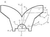
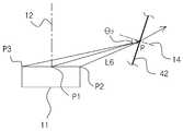
도 1을 참조하면, 본 발명에 따른 측면 방출용 발광다이오드(Light Emitting Diode, LED)용 렌즈(10)는 엘이디(11)에서 발산하는 광이 입사하는 밑면(20), 밑면(20)으로 입사한 광 중 직접 입사하는 광(L1)을 반사시키는 상면(30) 및 밑면(20)과 상면(30)을 연결하는 측면(40)을 포함한다.1, a
또한 측면(40)은 상면(30)에 연결되어 상면(30)에서 반사된 광(L2)이 출사하는 상부출사면(41)과, 밑면(20)과 상부출사면(41)에 연결되어 밑면(20)으로 입사하여 측면(40)으로 직접 입사되는 광(L3)을 렌즈(10) 외부로 출사시키는 하부출사면(42)을 포함한다.The
밑면(20)에는 상방으로 볼록한 홈부(21)가 구비될 수 있으며, 상기 홈부(21)는 엘이디(11)를 수용하기 위한 공간일 수 있으며, 엘이디(11)에서 발산된 광이 밑면(20)으로 입사할 때 원하는 방향으로 굴절시키기 위한 구성일 수도 있으며, 그 형상은 구면, 비구면 등 다양한 형태로 이루어질 수 있으며, 본 발명은 그에 한정하지 않는다.The
상면(30)은 코팅 또는 별도의 부재를 이용하여 직접 입사하는 광을 반사시키도록 구비될 수도 있으나, 입사한 광을 전반사시키도록 광학적으로 설계됨이 바람직하다. 또한 하부출사면(42)은 직접 입사한 광을 렌즈(10) 외부로 출사시키도록 광학적으로 설계됨이 바람직하다. 이에 대한 상세한 설명은 후술한다.The
상면(30)은 엘이디(11)의 광축(12)에 대칭으로 이루어져 엘이디(11)로부터 발산하는 광 중 광축(12)을 기준으로 소정각도 범위 내로 발산하는 중심영역의 광을 반사시키는 구성이며, 하부출사면(42)은 엘이디(11)에서 발산하는 광 중 상기 중심영역 외의 영역으로 발산하는 주변영역의 광을 렌즈(10) 외부로 출사시키는 구성이다.The
또한 본 발명에 따른 렌즈(10)는 밑면(20)과 하부출사면(42)의 연결부위로부터 하방으로 연장되어 렌즈(10)를 지지하는 레그(50)를 더 포함할 수 있다.The
바람직하게, 하부출사면(42)은 하방으로 갈수록 내측으로 기울어진 향상으로 이루어질 수 있다. 예를 들어, 하부출사면(42)은 엘이디(11)의 광축(12)을 기준으로 상방으로 갈수록 일정한 기울기로 벌어지는 경사면으로 이루어지거나 또는 하방으로 만곡된 형상으로 이루어질 수 있다. 또한 상부출사면(41)은 상면(30)에 연결되어 하방으로 연장되는 제1상부출사면(43)과, 제1상부출사면(43)과 하부출사면(42)을 연결하되 내측으로 단차지는 단차부(44)를 포함하여 이루어짐이 바람직하다. 그러면 하부출사면(42)과 단차부(44)에 의해 전체적인 볼륨(volume)이 작아져 재료비를 절감할 수 있게 된다.Preferably, the
발광다이오드용 렌즈는 유리, 아크릴(Methylmethacrylate), PMMA(Polymethylmethacrylate), PC(Polycarbonate), PET(Poly Ethylen Terephthalate) 등의 투과율이 우수한 투명한 물질로 사출성형(injection molding)에 의해 일체로(one-body) 제작됨이 일반적인데, 이와 같이 렌즈를 사출성형으로 제작시 본 발명에 따른 렌즈(10)는 선행기술들과 비교하여 볼륨을 줄여 재료비를 절감할 수 있을 뿐만 아니라 제조가 용이하다는 장점을 제공한다.The light-emitting diode lens is a transparent material having excellent transmittance such as glass, acrylic resin, polymethylmethacrylate (PMMA), polycarbonate (PC), and polyethyleneterephthalate (PET) When the lens is manufactured by injection molding, the
이하 본 발명에 따른 렌즈의 효과를 도면을 참조하여 상세히 설명한다.Hereinafter, effects of the lens according to the present invention will be described in detail with reference to the drawings.
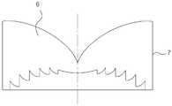
도 2 내지 5는 본 발명에 따른 렌즈의 효과를 설명하기 위한 도면으로서, 도 2는 선행기술1을 사출성형으로 제작하는 상태를 개략적으로 나타내는 도면이고, 도 3은 선행기술2를 사출성형으로 제작하는 상태를 개략적으로 나타내는 도면이고, 도 4는 선행기술3을 나타내는 도면이고, 도 5는 본 발명에 따른 렌즈를 사출성형으로 제작하는 상태를 개략적으로 나타내는 도면이다.FIGS. 2 to 5 are views for explaining the effect of the lens according to the present invention. FIG. 2 is a view schematically showing a state in which the
도 2에서 보이는 바와 같이, 선행기술1(미국등록특허 제6679621호)에 따른 렌즈(1)를 사출성형으로 제조시에는 사출성형 후 각각 상부와 하부로 분리되는 상부금형(51)과 하부금형(52)뿐만 아니라 사출성형 후 측면으로 슬라이딩되어 분리되는 슬라이딩금형(53)도 필요하다. 이는 선행기술1에 따른 렌즈(1)가 측면에 내측으로 기울어지는 제1굴절면(2)과, 외측으로 볼록한 형상으로 하방으로 연장되는 제2굴절면(3)의 형상 때문이다. 그리고 렌즈를 사출성형으로 제작시 슬라이딩금형(53)까지 필요하게 되면, 금형제작을 위한 추가적인 비용뿐만 아니라 제조공정이 복잡해지게 되어 바람직하지 않다.2, when the
또한, 도 3에서 보이는 바와 같이, 선행기술1에 따른 문제점을 보완한 선행기술2(한국등록특허 제10-0651550호)에 따른 렌즈(4)의 경우에도 아치형상의 하부굴절면(5)에 의해 사출성형시 슬라이딩금형(53)이 필요하다.3, in the case of the
또한, 도 4에서 보이는 바와 같이, 측면 방출형 엘이디 렌즈에 대한 다른 형태로서 선행기술3(한국등록특허 제10-0688767호)에 따른 렌즈(6)의 형태가 개시되는데, 이러한 선행기술3에 따른 렌즈(6)의 경우에는 선행기술1 및 2의 형태와는 달리 측면이 엘이디의 광축과 평행하기 때문에 사출성형시 슬라이딩금형이 필요없이 상하부금형만으로 제작할 수 있는 장점은 있으나, 엘이디에서 발산된 광이 측면으로 입사하지 않도록 거의 모든 광을 상면으로 입사시켜야 하고, 또한 상면으로 입사된 모든 광을 측면으로 반사시켜야 한다는 점에서 전체적인 볼륨이 커져야만 하는 문제가 있다.As shown in FIG. 4, the
반면, 도 5에서 보이는 바와 같이, 본 발명에 따른 렌즈(10)는 선행기술1 및 2와 달리 상하부금형(51,52)만을 사용하여도 사출성형이 가능하다. 이는 본 발명에 따른 렌즈(10)의 측면(40) 형상 예를 들어, 하부출사면(42)의 형상이 내측으로 기울어진 형태로 이루어지기 때문에 가능한 것이다.5, the
또한 본 발명에 따른 렌즈(10)는 선행기술3과 달리 측면(40)의 형상 예를 들어, 단차부(44)와 하부출사면(42)의 형상이 대략 내측으로 기울어진 형태로 이루어지기 때문에 볼륨을 줄일 수 있게 된다.The
또한 본 발명에 따른 렌즈(10)는 엘이디(11)에서 발산한 광 중 중심영역의 광은 상면(30)에서 반사되어 측면(40)으로 출사되며, 주변영역의 광은 하부출사면(42)에서 직접 렌즈(10) 외부로 출사하기 때문에, 선행기술3과 달리 엘이디(11)에서 발산하는 모든 광을 직접 상면(30)으로만 입사시켜 반사시킬 필요가 없기 때문에 더더욱 전체적인 부피를 줄일 수 있게 된다.In the
상술한 바와 같이, 본 발명에 따른 렌즈(10)는 선행기술들과 비교하여 전체적인 부피를 줄일 수 있으면서도 제조가 용이하다는 장점을 가진다. 이하에서는 본 발명에 따른 렌즈의 구성에 대하여 상세히 설명한다.As described above, the
상면(30)은 입사한 광을 전반사시키도록 광학적으로 설계됨이 바람직하다. 이하 도면을 참조하여 이러한 상면(30)의 실시 예들을 상세히 설명한다.The
도 6은 상면의 일실시 예를 설명하기 위한 도면이다.6 is a view for explaining an embodiment of the upper surface.
도 6을 참조하면, 엘이디(11)의 광축(12)과 엘이디(11)의 교점을 제1기준점(P1)으로 하였을 때, 상면(30) 상의 임의의 점(P)과 제1기준점(P1)을 연결하는 직선과 광축(12)이 이루는 각을 α1, 상면(30) 상의 임의의 점(P)과 제1기준점(P1)의 거리를 R1, 상기 α1의 증분을 Δα1, Δα1에 대한 R1의 증분(감소량 또는 증가량)을 ΔR1, 상면(30) 상의 임의의 점(P)에서의 법선(13)과 상기 직선 즉, 상면(30) 상의 임의의 점(P)과 제1기준점(P1)을 연결하는 직선이 이루는 각을 β1, 렌즈(10)를 이루는 재료의 굴절률을 n으로 하면, 상면(30)은 ΔR1 / (R1Δα1) 〉 1 / √(n2-1) 조건을 만족하도록 구성될 수 있다.6, when an intersection point between the
도 7 및 도 8은 상면의 다른 실시 예를 설명하기 위한 도면이다.Figs. 7 and 8 are views for explaining another embodiment of the upper surface. Fig.
도 6에서 설명된 실시 예와 달리, 도 7 및 도 8에 따른 상면(30)의 광학적 조건은 엘이디(11)의 광원을 점광원이 아닌 면광원으로 고려할 때 적용가능한 조건이다. 실제로 렌즈(10)는 엘이디(11)보다 매우 큰 볼륨으로 이루어지지는 않기 때문에, 렌즈(10) 설계시 이와 같이 엘이디(11) 광원을 면광원으로 고려하여야 함이 바람직하다.Unlike the embodiment described in Fig. 6, the optical condition of the
먼저, 도 7을 참조하면, 엘이디(11)의 광원을 점광원이 아닌 면광원으로 고려할 때에는 엘이디(11)의 중심점 즉, 제1기준점(P1)에서 발산하는 광뿐만 아니라 엘이디(11)의 양끝점(P2,P3)에서 발산하는 광도 고려하여야 하며, 이 경우 광축(12)을 기준으로 상기 임의의 점(P)과 같은 측의 엘이디(11) 끝점(P2)에서 발산하여 상기 임의의 점(P)으로 입사하는 광(L5)이 상기 임의의 점(P)에서의 법선(13)과 이루는 각(θ1)이, 제1기준점(P1)과 다른 측 끝점(P3)에서 발산하여 입사하는 경우보다 작음을 알 수 있다. 따라서 상면(30)이 같은 측 엘이디(11) 끝점(P2)에서 발산하여 입사하는 광(L5)을 전반사하도록 구비된다면, 엘이디(11) 광원을 면광원으로 고려한다 하더라도 상면(30)은 엘이디(11)에서 발산하여 상면(30)으로 입사하는 거의 모든 광을 전반사시킬 수 있게 된다.7, when the light source of the
이러한 광학적 조건을 도 8을 참조하여 설명하면, 광축(12)을 기준으로 상면(30) 상의 임의의 점(P)과 같은 측의 엘이디(11)의 끝점(P2)을 제2기준점(P2)으로 하였을 때, 상면(30) 상의 임의의 점(P)과 제2기준점(P2)을 연결하는 직선과 기준축(15)이 이루는 각을 α2, 상면(30) 상의 임의의 점(P)과 제2기준점(P2)의 거리를 R2, 상기 α2의 증분을 Δα2, Δα2에 대한 R2의 증분을 ΔR2, 렌즈(10)를 이루는 재료의 굴절률을 n으로 하면, 상면(30)은 ΔR2 / (R2Δα2) 〉 1 / √(n2-1) 조건을 만족하도록 구성될 수 있다.8, the end point P2 of the
마찬가지로, 하부출사면(42)도 직접 입사한 광을 렌즈(10) 외부로 출사시키도록 광학적으로 설계됨이 바람직하다. 이하 도면을 참조하여 이러한 하부출사면(42)의 실시 예들을 상세히 설명한다.Likewise, it is preferable that the
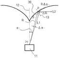
도 9는 하부출사면의 일실시 예를 설명하기 위한 도면이다. 도 9를 참조하면, 광축(12)과 엘이디(11) 교점을 제1기준점(P1)으로 하였을 때, 하부출사면(42) 상의 임의의 점(P)과 제1기준점(P1)을 연결하는 직선과 광축(12)과 수직한 수평축(16)이 이루는 각을 α3, 하부출사면(42) 상의 임의의 점(P)과 제1기준점(P1)의 거리를 R3, 상기 α3의 증분을 Δα3, Δα3에 대한 R3의 증분을 ΔR3, 렌즈(10)를 이루는 재료의 굴절률을 n으로 하면, 하부출사면(42)은 ΔR3 / (R3Δα3) 〈 1 / √(n2-1) 조건을 만족하도록 구성될 수 있다.9 is a view for explaining an embodiment of a lower emission surface. 9, when a point of intersection between the
도 10 및 도 11은 하부출사면의 다른 실시 예를 설명하기 위한 도면이다.10 and 11 are views for explaining another embodiment of the lower emission surface.
도 9에서 설명된 실시 예와 달리, 도 10 및 도 11에 따른 하부출사면(42)의 광학적 조건은 엘이디(11)의 광원을 점광원이 아닌 면광원으로 고려할 때 적용가능한 조건이다.Unlike the embodiment described in Fig. 9, the optical condition of the
먼저, 도 10을 참조하면, 엘이디(11)의 광원을 점광원이 아닌 면광원으로 고려할 때에는 엘이디(11)의 중심점 즉, 제1기준점(P1)에서 발산하는 광뿐만 아니라 엘이디(11)의 양끝점(P2,P3)에서 발산하는 광도 고려하여야 하며, 이 경우 광축(12)을 기준으로 하부출사면(42) 상의 임의의 점(P)과 같은 측의 엘이디(11) 끝점(P2)에서 발산하여 상기 임의의 점(P)으로 입사하는 광(L6)이 상기 임의의 점(P)에서의 법선(14)과 이루는 각(θ2)이, 제1기준점(P1)과 반대 측 끝점(P3)에서 발산하여 입사하는 경우보다 가장 큼을 알 수 있다. 따라서 하부출사면(42)이 같은 측 엘이디(11) 끝점(P2)에서 발산하여 입사하는 광(L6)을 렌즈(10) 외부로 출사시키도록 이루어진다면, 엘이디(11) 광원을 면광원으로 고려한다 하더라도 하부출사면(42)은 엘이디(11)에서 발산하여 하부출사면(42)으로 직접 입사하는 거의 모든 광을 렌즈(10) 외부로 출사시킬 수 있게 된다.10, when the light source of the
이러한 광학적 조건을 도 11을 참조하여 설명하면, 광축(12)을 기준으로 하부출사면(42) 상의 임의의 점(P)과 같은 측의 엘이디(11)의 끝점(P2)을 제2기준점(P2)으로 하였을 때, 하부출사면(42) 상의 임의의 점(P)과 제2기준점(P2)을 연결하는 직선과 광축(12)과 수직한 수평축(16)이 이루는 각을 α4, 하부출사면(42) 상의 임의의 점(P)과 제2기준점(P2)의 거리를 R4, 상기 α4의 증분을 Δα4, Δα4에 대한 R4의 증분을 ΔR4, 렌즈(10)를 이루는 재료의 굴절률을 n으로 하면, 하부출사면(42)은 ΔR4 / (R4Δα4) 〈 1 / √(n2-1) 조건을 만족하도록 구성될 수 있다.11, the end point P2 of the
도 12는 단차부를 확대한 부분확대도이다.12 is a partially enlarged view of an enlarged step.
도 12를 참조하면, 단차부(44)는 상면(30)에서 반사된 광을 출사시키는 다수의 불연속한 제2상부출사면(45)과, 제2상부출사면(45)을 연결하는 연결면(46)을 포함하여 이루어질 수 있다.12, the
제2상부출사면(45)은 엘이디(11) 광축(12)과 평행하거나 또는 내측으로 기울어진 형상으로 이루어지는 것이 바람직하다. 그러면 사출성형으로 렌즈(10) 제작시 상하부금형(51,52)만으로 제작이 가능하여 제조공정이 간단해질 수 있다.It is preferable that the second
연결면(46)은 상면(30)에서 반사된 광(L2)의 주광(chief ray)의 경로와 평행하게 이루어지는 것이 바람직하다. 그러면 상면(30)에서 반사된 거의 모든 광(L2)이 제2상부출사면(45)으로 입사하여 출사할 수 있기 때문에 광(L2)의 출사각을 제어하기가 용이하며, 광(L2)이 연결면(46)으로 입사함으로써 발생하는 광손실을 줄일 수 있게 된다. 여기서, 주광(chief ray)의 경로란 상면(30) 상의 어느 한 지점으로부터 반사된 광(l2)들의 경로 중 센터광이 지나가는 경로를 말한다.The
도 13 및 도 14는 단차부의 실시 예들을 설명하기 위한 도면이다.Figs. 13 and 14 are views for explaining embodiments of a step portion.
먼저, 도 13을 참조하면, 하부출사면(42)과 단차부(44)의 접점인 단차부(44)의 시작단(47)과 상기 다수의 연결면(46) 중 최상단에 위치하는 연결면(46)의 상단(48)을 연결하는 가상의 연결선(17)이 엘이디(11)의 광축(12)과 평행한 가상의 기준축(15)과 이루는 각(θ3)은, 엘이디(11)와 광축(12)의 교점인 제1기준점(P1)에서 발산되어 하부출사면(42)의 상단인 상기 시작단(47)으로 입사하는 광(L7)이 기준축(15)과 이루는 각(θ4)보다 크게 이루어지고, 상기 각각의 제2상부출사면(45)의 상단 또는 연결면(46)의 상단은 기준축(15)을 기준으로 연결선(17)보다 외측에 존재하는 것이 바람직하다. 그러면 엘이디(11)에서 발산된 광 중 단차부(44)로 직접 입사하여 출사하는 광은 없게 되고, 그에 따라 단차부(44)로 직접 입사하여 출사함으로써 발생하는 광손실을 줄일 수 있게 된다.13, the starting
도 13에서 설명된 실시 예와 달리, 도 14에 따른 단차부(44)의 조건은 엘이디(11)의 광원을 점광원이 아닌 면광원으로 고려할 때 적용가능한 조건이다. 즉, 엘이디(11)의 광원을 점광원이 아닌 면광원으로 고려할 때에는 엘이디(11)의 중심점인 제1기준점(P1)에서 발산하는 광뿐만 아니라 엘이디(11)의 양끝점(P2,P3)에서 발산하는 광도 고려하여야 하며, 이 경우 시작단(47)과 반대 측의 엘이디(11)의 끝점(P3)에서 발산하여 시작단(47)으로 입사하는 광(L8)이 기준축(15)과 이루는 각(θ6)이, 제1기준점(P1)과 같은 측 끝점(P2)에서 발산하여 시작단(47)으로 입사하는 광이 기준축(15)과 이루는 각(θ4,θ5)보다 큼을 알 수 있다. 따라서 상기 가상의 연결선(17)이 기준축(15)과 이루는 각(θ3)은, 광축(12)을 기준으로 시작단(47)과 반대 측의 엘이디(11)의 끝점을 제3기준점(P3)으로 하였을 때 상기 제3기준점(P3)에서 발산하여 시작단(47)으로 입사하는 광(L8)이 기준축(15)과 이루는 각(θ6)보다 크게 이루어지고, 상기 각각의 제2상부출사면(45)의 상단 또는 연결면(46)의 상단은 기준축(15)을 기준으로 연결선(17)보다 외측에 존재하면, 엘이디(11)의 광원을 면광원으로 고려한다 하더라도 단차부(44)로 직접 입사하여 출사하는 광은 없게 되고, 그에 따라 단차부(44)로 직접 입사하여 출사함으로써 발생하는 광손실을 줄일 수 있게 된다.Unlike the embodiment described in Fig. 13, the condition of the
한편, 하부출사면(42)은 엘이디(11)에서 발산하여 직접 입사하는 광(L3)을 출사시킴에 있어서, 출사된 광이 다시 단차부(44)로 입사하지 않도록 다음 조건을 만족하도록 구성됨이 바람직하다.On the other hand, the
도 15는 이러한 하부출사면의 조건을 설명하기 위한 도면이다.Fig. 15 is a view for explaining conditions of such a lower exit surface.
도 15를 참조하면, 상기 다수의 불연속한 제2상부출사면(45) 중 최하단에 위치하는 제2상부출사면(45)의 하단(19)과 제1상부출사면(43)의 하단(49)을 연결하는 가상의 연결선(18)이 엘이디(11)의 광축(12)과 수직한 수평축(16)과 이루는 각을 θ7, 엘이디(11)와 광축(12)의 교점을 제1기준점(P1)으로 하였을 때 상기 제1기준점(P1)에서 발산하여 하부출사면(42) 상의 임의의 점(P)으로 직접 입사하는 광(L3)이 상기 임의의 점(P)에서의 법선(14)과 이루는 각을 θ8, 상기 임의의 점(P)에서의 접선이 광축(12)과 평행한 가상의 기준축(15)과 이루는 각을 Δα, 상기 임의의 점(P)으로 입사된 광(L3)이 하부출사면(42)을 통해 출사한 광(L4)이 법선(14)과 이루는 굴절각을 θ9, 상기 출사한 광(L4)이 수평축(16)과 이루는 각을 θ, 렌즈(10)를 이루는 재료의 굴절률을 n이라 하면, 다음 식을 만족한다.15, the
n×sinθ8= sinθ9n x sin?8 = sin?9
θ9= θ + Δαθ9 = θ + Δα
여기서, 하부출사면(42)을 통해 출사된 광(L4)이 다시 단차부(44)로 입사하지 않기 위해서는 상기 광(L4)이 수평축(16)과 이루는 각(θ)이 상기 연결선(18)이 엘이디(11)의 광축(12)과 수직한 수평축(16)과 이루는 각(θ7)보다 같거나 작아야 한다. 즉, θ ≤ θ7조건을 만족하여야 한다.In order that the light L4 emitted through the
따라서, 상기 식들과 상기 조건을 정리하면, 하부출사면(42)은 출사된 광(L4)이 단차부(44)로 입사하지 않도록 Δα ≥ sin-1(n×sinθ8) ― θ7 조건을 만족하도록 구성됨이 바람직하다.Therefore, by summarizing the above equations and the above conditions, the
여기서, Δα는 하부출사면(42) 상의 임의의 점(P)에서의 접선이 기준축(15)과 이루는 각을 의미하며, 따라서 하부출사면(42)은 도 1에서 보이는 바와 같이, Δα이 일정한 값을 가지는 경사면으로 이루어질 수도 있으며, Δα이 일정한 값을 가지지 않는 구면 또는 비구면으로도 이루어질 수 있다.Here, ?? refers to the angle formed by the tangent at an arbitrary point P on the
한편, 상기 하부출사면(42)의 조건은 엘이디(11)의 광원을 점광원이 아닌 면광원으로 고려할 때 적용가능한 조건이다. 따라서 엘이디(11)의 광원을 점광원이 아닌 면광원으로 고려할 때에는 엘이디(11)의 중심점 즉, 제1기준점(P1)에서 발산하는 광뿐만 아니라 엘이디(11)의 양끝점(P2,P3)에서 발산하는 광도 고려하여야 하며, 이 경우 도 10에서 보이는 바와 같이, 하부출사면(42) 상의 임의의 점(P)과 같은 측의 엘이디(11) 끝점(P2)에서 발산하여 상기 임의의 점(P)으로 입사하는 광(L6)이 상기 임의의 점(P)에서의 법선(14)과 이루는 각(θ2)이, 제1기준점(P1)과 반대 측 끝점(P3)에서 발산하여 입사하는 경우보다 가장 큼을 알 수 있다. 따라서 같은 측 엘이디(11) 끝점(P2)을 제2기준점(P2)라고 하였을 때, 상기 제2기준점(P2)에서 발산하여 하부출사면(42)으로 직접 입사되어 출사된 광(L4)이 수평축(16)과 이루는 각(θ)이 상기 연결선(18)이 수평축(16)과 이루는 각(θ7)보다 같거나 작게 이루어진다면, 엘이디(11) 광원을 면광원으로 고려한다 하더라도 하부출사면(42)은 엘이디(11)에서 발산하여 하부출사면(42)으로 직접 입사하는 거의 모든 광을 단차부(44)로 입사하지 않도록 출사시킬 수 있게 된다.On the other hand, the condition of the
도 16은 본 발명의 다른 실시 예에 따른 렌즈를 나타내는 수직단면도로서, 하부출사면(42)의 Δα이 일정한 값을 가지지 않는 실시 예가 도시되며, 도 16과 같이 하부출사면(42)은 하방으로 만곡된 형상을 가지는 형상으로도 이루어질 수 있다.16 is a vertical cross-sectional view showing a lens according to another embodiment of the present invention, in which an angle DELTA alpha of the
도 17 및 도 18은 본 발명의 일실시 예에 따른 렌즈의 개략적인 평면도이다.17 and 18 are schematic plan views of a lens according to an embodiment of the present invention.
도 17 및 도 18을 참조하면, 본 발명의 일실시 예에 따른 렌즈(10)는 수평단면상 대략 원형의 형상으로 이루어질 수 있으며, 레그(50)는 도 17에서 보이는 바와 같이, 엘이디(11)로부터 일정한 거리에 소정각도 간격으로 복수개 구비될 수도 있으며, 도 18에서 보이는 바와 같이, 엘이디(11)로부터 일정한 거리에 연속적으로 즉, 대략 원형의 띠 형상으로 구비될 수도 있다.17 and 18, the
이상에서 살펴본 바와 같이, 본 발명은 전체적인 볼륨을 줄일 수 있으면서도 제조가 용이한 측면 방출형 발광다이오드용 렌즈에 관한 것으로서, 그 실시 형태는 다양한 형태로 변경가능하다 할 것이다. 따라서 본 발명은 본 명세서에서 개시된 실시 예에 의해 한정되지 않으며, 본 발명이 속하는 기술분야에서 통상의 지식을 가진 자가 변경 가능한 모든 형태도 본 발명의 권리범위에 속한다 할 것이다.While the present invention has been particularly shown and described with reference to exemplary embodiments thereof, it is to be understood that the invention is not limited to the disclosed exemplary embodiments. Accordingly, the present invention is not limited to the embodiments disclosed herein, and all changes which can be made by those skilled in the art are also within the scope of the present invention.
10 : 렌즈 11 : 발광다이오드
12 : 광축 20 : 밑면
30 : 상면 40 : 측면
41 : 상부출사면 42 : 하부출사면
43 : 제1상부출사면 44 : 단차부
45 : 제2상부출사면 46 : 연결면10: lens 11: light emitting diode
12: optical axis 20: bottom surface
30: upper surface 40: side surface
41: upper emission surface 42: lower emission surface
43: first upper exit surface 44: stepped portion
45: second upper exit surface 46: connecting surface
Claims (17)
Translated fromKorean상기 발광다이오드에서 발산하는 광이 입사하는 밑면;
상기 밑면으로 입사한 광 중 직접 입사하는 광을 반사시키는 상면; 및
상기 밑면과 상기 상면을 연결하는 측면;을 포함하고,
상기 측면은 상기 상면에 연결되어 상기 상면에서 반사된 광이 출사하는 상부출사면과, 상기 밑면과 상기 상부출사면에 연결되어 상기 밑면으로 입사하여 상기 측면으로 직접 입사되는 광이 출사하는 하부출사면을 포함하고,
상기 하부출사면은 상방으로 갈수록 상기 발광다이오드의 광축을 기준으로 벌어지는 형상으로 이루어지고,
상기 발광다이오드의 광축과 상기 발광다이오드의 교점을 제1기준점(P1)으로 하였을 때, 상기 상면 상의 임의의 점과 상기 제1기준점(P1)을 연결하는 직선과 상기 광축이 이루는 각을 α1, 상기 상면 상의 임의의 점과 상기 제1기준점(P1)의 거리를 R1, 상기 α1의 증분을 Δα1, Δα1에 대한 R1의 증분을 ΔR1, 상기 렌즈를 이루는 재료의 굴절률을 n으로 하면,
상기 상면은 ΔR1 / (R1Δα1) 〉 1 / √(n2-1) 조건을 만족하도록 구성되는 것을 특징으로 하는 측면 방출형 발광다이오드용 렌즈.A side-emitting type light emitting diode lens for emitting light emitted from a light emitting diode (LED) to a side surface,
A bottom surface on which light emitted from the light emitting diode is incident;
An upper surface reflecting light directly incident on the bottom surface; And
And a side surface connecting the bottom surface and the top surface,
The side surface is connected to the upper surface and has an upper exit surface through which light reflected from the upper surface is emitted, and a lower exit surface connected to the lower surface and the upper exit surface to enter the bottom surface, / RTI >
Wherein the lower emission surface has a shape extending upward with respect to an optical axis of the light emitting diode,
Wherein an angle formed by a straight line connecting an arbitrary point on the upper surface with the first reference point (P1) and the optical axis is defined as α1 , the arbitrary point and the refractive index of the first reference point (P1) the increment of R1 for the increment of the α1 on Δα1, Δα1 ΔR1, the R1, the distance constituting the lens material on the upper surface of n In this case,
Wherein the upper surface is configured to satisfy a condition of? R1 / (R1 ??1 )> 1 /? (N2 -1).
상기 발광다이오드에서 발산하는 광이 입사하는 밑면;
상기 밑면으로 입사한 광 중 직접 입사하는 광을 반사시키는 상면; 및
상기 밑면과 상기 상면을 연결하는 측면;을 포함하고,
상기 측면은 상기 상면에 연결되어 상기 상면에서 반사된 광이 출사하는 상부출사면과, 상기 밑면과 상기 상부출사면에 연결되어 상기 밑면으로 입사하여 상기 측면으로 직접 입사되는 광이 출사하는 하부출사면을 포함하고,
상기 하부출사면은 상방으로 갈수록 상기 발광다이오드의 광축을 기준으로 벌어지는 형상으로 이루어지고,
상기 발광다이오드의 광축을 기준으로 상기 상면 상의 임의의 점과 같은 측의 상기 발광다이오드의 끝점을 제2기준점(P2)으로 하였을 때, 상기 상면 상의 임의의 점과 상기 제2기준점(P2)을 연결하는 직선과 상기 광축과 평행한 가상의 기준축이 이루는 각을 α2, 상기 상면 상의 임의의 점과 상기 제2기준점(P2)의 거리를 R2, 상기 α2의 증분을 Δα2, Δα2에 대한 R2의 증분을 ΔR2, 상기 렌즈를 이루는 재료의 굴절률을 n으로 하면,
상기 상면은 ΔR2 / (R2Δα2) 〉 1 / √(n2-1) 조건을 만족하도록 구성되는 것을 특징으로 하는 측면 방출형 발광다이오드용 렌즈.A side-emitting type light emitting diode lens for emitting light emitted from a light emitting diode (LED) to a side surface,
A bottom surface on which light emitted from the light emitting diode is incident;
An upper surface reflecting light directly incident on the bottom surface; And
And a side surface connecting the bottom surface and the top surface,
The side surface is connected to the upper surface and has an upper exit surface through which light reflected from the upper surface is emitted, and a lower exit surface connected to the lower surface and the upper exit surface to enter the bottom surface, / RTI >
Wherein the lower emission surface has a shape extending upward with respect to an optical axis of the light emitting diode,
When an end point of the light emitting diode on the same side as an arbitrary point on the upper surface is defined as a second reference point (P2) with respect to an optical axis of the light emitting diode, an arbitrary point on the upper surface and the second reference point And a virtual reference axis parallel to the optical axis is α2 , a distance between an arbitrary point on the upper surface and the second reference point is R2 , an increment of α2 is Δα2 , Δα2 an increment of R2 for ΔR2, assuming that the refractive index of the material of the lens to n,
Wherein the upper surface is configured to satisfy a condition of? R2 / (R2 ??2 )> 1 /? (N2 -1).
상기 발광다이오드에서 발산하는 광이 입사하는 밑면;
상기 밑면으로 입사한 광 중 직접 입사하는 광을 반사시키는 상면; 및
상기 밑면과 상기 상면을 연결하는 측면;을 포함하고,
상기 측면은 상기 상면에 연결되어 상기 상면에서 반사된 광이 출사하는 상부출사면과, 상기 밑면과 상기 상부출사면에 연결되어 상기 밑면으로 입사하여 상기 측면으로 직접 입사되는 광이 출사하는 하부출사면을 포함하고,
상기 하부출사면은 상방으로 갈수록 상기 발광다이오드의 광축을 기준으로 벌어지는 형상으로 이루어지고,
상기 발광다이오드의 광축과 상기 발광다이오드의 교점을 제1기준점(P1)으로 하였을 때, 상기 하부출사면 상의 임의의 점과 상기 제1기준점(P1)을 연결하는 직선과 상기 광축과 수직한 수평축이 이루는 각을 α3, 상기 하부출사면 상의 임의의 점과 상기 제1기준점(P1)의 거리를 R3, 상기 α3의 증분을 Δα3, Δα3에 대한 R3의 증분을 ΔR3, 상기 렌즈를 이루는 재료의 굴절률을 n으로 하면,
상기 하부출사면은 ΔR3 / (R3Δα3) 〈 1 / √(n2-1) 조건을 만족하도록 구성되는 것을 특징으로 하는 측면 방출형 발광다이오드용 렌즈.A side-emitting type light emitting diode lens for emitting light emitted from a light emitting diode (LED) to a side surface,
A bottom surface on which light emitted from the light emitting diode is incident;
An upper surface reflecting light directly incident on the bottom surface; And
And a side surface connecting the bottom surface and the top surface,
The side surface is connected to the upper surface and has an upper exit surface through which light reflected from the upper surface is emitted, and a lower exit surface connected to the lower surface and the upper exit surface to enter the bottom surface, / RTI >
Wherein the lower emission surface has a shape extending upward with respect to an optical axis of the light emitting diode,
Wherein a straight line connecting an arbitrary point on the lower exit surface with the first reference point (P1) and a horizontal axis perpendicular to the optical axis (P1) are defined as a first reference point (P1) at an intersection of the optical axis of the light emitting diode for the angle α3, the R3 increments of the increment of the α3 to Δα3, Δα3 ΔR3, the distance of any point from the first reference point (P1) on the lower output surface R3, wherein Assuming that the refractive index of the material forming the lens is n,
Wherein the lower exit surface is configured to satisfy a condition of? R3 / (R3 ??3 ) <1 /? (N2 -1).
상기 발광다이오드에서 발산하는 광이 입사하는 밑면;
상기 밑면으로 입사한 광 중 직접 입사하는 광을 반사시키는 상면; 및
상기 밑면과 상기 상면을 연결하는 측면;을 포함하고,
상기 측면은 상기 상면에 연결되어 상기 상면에서 반사된 광이 출사하는 상부출사면과, 상기 밑면과 상기 상부출사면에 연결되어 상기 밑면으로 입사하여 상기 측면으로 직접 입사되는 광이 출사하는 하부출사면을 포함하고,
상기 하부출사면은 상방으로 갈수록 상기 발광다이오드의 광축을 기준으로 벌어지는 형상으로 이루어지고,
상기 발광다이오드의 광축을 기준으로 상기 하부출사면 상의 임의의 점과 같은 측의 상기 발광다이오드의 끝점을 제2기준점(P2)으로 하였을 때, 상기 하부출사면 상의 임의의 점과 상기 제2기준점(P2)을 연결하는 직선과 상기 광축과 수직한 수평축이 이루는 각을 α4, 상기 하부출사면 상의 임의의 점과 상기 제2기준점(P2)의 거리를 R4, 상기 α4의 증분을 Δα4, Δα4에 대한 R4의 증분을 ΔR4, 상기 렌즈를 이루는 재료의 굴절률을 n으로 하면,
상기 하부출사면은 ΔR4 / (R4Δα4) 〈 1 / √(n2-1) 조건을 만족하도록 구성되는 것을 특징으로 하는 측면 방출형 발광다이오드용 렌즈.A side-emitting type light emitting diode lens for emitting light emitted from a light emitting diode (LED) to a side surface,
A bottom surface on which light emitted from the light emitting diode is incident;
An upper surface reflecting light directly incident on the bottom surface; And
And a side surface connecting the bottom surface and the top surface,
The side surface is connected to the upper surface and has an upper exit surface through which light reflected from the upper surface is emitted, and a lower exit surface connected to the lower surface and the upper exit surface to enter the bottom surface, / RTI >
Wherein the lower emission surface has a shape extending upward with respect to an optical axis of the light emitting diode,
And a second reference point (P2), wherein an end point of the light emitting diode on the same side as an arbitrary point on the lower exit surface with respect to an optical axis of the light emitting diode is a second reference point (P2) P2) and a horizontal axis perpendicular to the optical axis is α4 , a distance between an arbitrary point on the lower emission surface and the second reference point (P2) is R4 , the increment of α4 is Δα4 , the increment of R4 to Δα4 ΔR4, assuming that the refractive index of the material of the lens to n,
Wherein the lower exit surface satisfies the following condition: DELTA R4 / (R4 DELTA alpha4 ) <1 / (n2 -1).
상기 하부출사면은 상방으로 갈수록 상기 발광다이오드의 광축을 기준으로 벌어지는 경사면으로 이루어지거나 또는 하방으로 만곡된 형상으로 이루어지는 것을 특징으로 하는 측면 방출형 발광다이오드용 렌즈.6. The method according to any one of claims 2 to 5,
Wherein the lower exit surface is formed as an inclined surface extending toward the optical axis of the light emitting diode as it goes upward or curved downward.
상기 발광다이오드에서 발산하는 광이 입사하는 밑면;
상기 밑면으로 입사한 광 중 직접 입사하는 광을 반사시키는 상면; 및
상기 밑면과 상기 상면을 연결하는 측면;을 포함하고,
상기 측면은 상기 상면에 연결되어 상기 상면에서 반사된 광이 출사하는 상부출사면과, 상기 밑면과 상기 상부출사면에 연결되어 상기 밑면으로 입사하여 상기 측면으로 직접 입사되는 광이 출사하는 하부출사면을 포함하고,
상기 하부출사면은 상방으로 갈수록 상기 발광다이오드의 광축을 기준으로 벌어지는 형상으로 이루어지고,
상기 상부출사면은 상기 상면에 연결되어 하방으로 연장되는 제1상부출사면과, 상기 제1상부출사면과 상기 하부출사면을 연결하되 내측으로 단차지는 단차부를 포함하는 것을 특징으로 하는 측면 방출형 발광다이오드용 렌즈.A side-emitting type light emitting diode lens for emitting light emitted from a light emitting diode (LED) to a side surface,
A bottom surface on which light emitted from the light emitting diode is incident;
An upper surface reflecting light directly incident on the bottom surface; And
And a side surface connecting the bottom surface and the top surface,
The side surface is connected to the upper surface and has an upper exit surface through which light reflected from the upper surface is emitted, and a lower exit surface connected to the lower surface and the upper exit surface to enter the bottom surface, / RTI >
Wherein the lower emission surface has a shape extending upward with respect to an optical axis of the light emitting diode,
Wherein the upper emission surface comprises a first upper emission surface connected to the upper surface and extending downwardly and a stepped portion connected to the first upper emission surface and the lower emission surface and stepped inward, Lenses for light emitting diodes.
상기 단차부는 상기 상면에서 반사된 광을 출사시키는 다수의 불연속한 제2상부출사면과, 상기 제2상부출사면을 연결하는 연결면을 포함하는 것을 특징으로 하는 측면 방출형 발광다이오드용 렌즈.8. The method of claim 7,
Wherein the step portion includes a plurality of discontinuous second upper emission surfaces for emitting light reflected from the upper surface and a connection surface connecting the second upper emission surface.
상기 제2상부출사면은 상기 발광다이오드의 광축과 평행하거나 또는 상방으로 갈수록 상기 발광다이오드의 광축을 기준으로 벌어지는 형상으로 이루어지는 것을 특징으로 하는 측면 방출형 발광다이오드용 렌즈.9. The method of claim 8,
Wherein the second upper exit surface has a shape extending parallel to an optical axis of the light emitting diode or upward with respect to an optical axis of the light emitting diode.
상기 연결면은 상기 상면에서 반사된 광의 주광(chief ray)의 경로와 평행하게 이루어지는 것을 특징으로 하는 측면 방출형 발광다이오드용 렌즈.9. The method of claim 8,
Wherein the connection surface is parallel to a path of a chief ray of light reflected from the upper surface.
상기 하부출사면과 상기 단차부의 접점인 상기 단차부의 시작단과 상기 다수의 연결면 중 최상단에 위치하는 연결면의 상단을 연결하는 가상의 연결선이 상기 발광다이오드의 광축과 평행한 가상의 기준축과 이루는 각(θ3)은, 상기 발광다이오드와 상기 광축의 교점을 제1기준점(P1)으로 하였을 때 상기 제1기준점(P1)에서 발산되어 상기 하부출사면의 상단인 상기 시작단으로 입사하는 광이 상기 기준축과 이루는 각(θ4)보다 크고,
상기 각각의 제2상부출사면의 상단은 상기 기준축을 기준으로 상기 연결선보다 외측에 존재하는 것을 특징으로 하는 측면 방출형 발광다이오드용 렌즈.9. The method of claim 8,
And a virtual connecting line connecting the starting end of the stepped portion, which is the contact point between the lower emitting surface and the stepped portion, and the upper end of the connecting surface located at the uppermost one of the plurality of connecting surfaces, with an imaginary reference axis parallel to the optical axis of the light emitting diode The angle?3 is the angle at which the light emitted from the first reference point P1 and incident on the top end of the lower exit surface when the intersection of the light emitting diode and the optical axis is defined as the first reference point P1 Is larger than an angle (?4 ) formed with the reference axis,
Wherein an upper end of each second upper exit surface is located outside the connecting line with respect to the reference axis.
상기 하부출사면과 상기 단차부의 접점인 상기 단차부의 시작단과 상기 다수의 연결면 중 최상단에 위치하는 연결면의 상단을 연결하는 가상의 연결선이 상기 발광다이오드의 광축과 평행한 가상의 기준축과 이루는 각(θ3)은, 상기 시작단과 반대 측의 상기 발광다이오드의 끝점을 제3기준점(P3)으로 하였을 때 상기 제3기준점(P3)에서 발산하여 상기 하부출사면의 상단인 상기 시작단으로 입사하는 광이 상기 기준축과 이루는 각(θ6)보다 크고,
상기 각각의 제2상부출사면의 상단은 상기 기준축을 기준으로 상기 연결선보다 외측에 존재하는 것을 특징으로 하는 측면 방출형 발광다이오드용 렌즈.9. The method of claim 8,
And a virtual connecting line connecting the starting end of the stepped portion, which is the contact point between the lower emitting surface and the stepped portion, and the upper end of the connecting surface located at the uppermost one of the plurality of connecting surfaces, with an imaginary reference axis parallel to the optical axis of the light emitting diode The angle?3 is a distance from the third reference point P3 when the end point of the light emitting diode on the side opposite to the start end is the third reference point P3, Is larger than an angle (?6 ) formed between the reference axis
Wherein an upper end of each second upper exit surface is located outside the connecting line with respect to the reference axis.
상기 다수의 불연속한 제2상부출사면 중 최하단에 위치하는 제2상부출사면의 하단과 상기 제1상부출사면의 하단을 연결하는 가상의 연결선이 상기 발광다이오드의 광축과 수직한 수평축과 이루는 각을 θ7, 상기 발광다이오드와 상기 광축의 교점을 제1기준점(P1)으로 하였을 때 상기 제1기준점(P1)에서 발산하여 상기 하부출사면 상의 임의의 점으로 직접 입사하는 광이 상기 임의의 점에서의 법선과 이루는 각을 θ8, 상기 하부출사면 상의 임의의 점에서의 접선이 상기 광축과 평행한 가상의 기준축과 이루는 각을 Δα라 하면,
상기 하부출사면은 Δα ≥ sin-1(n×sinθ8) ― θ7 조건을 만족하도록 구성되는 것을 특징으로 하는 측면 방출형 발광다이오드용 렌즈.9. The method of claim 8,
And an imaginary connecting line connecting the lower end of the second upper exit surface located at the lowermost one of the plurality of discontinuous second upper exit surfaces and the lower end of the first upper exit surface with a horizontal axis perpendicular to the optical axis of the light emitting diode (7) , and the light emitted from the first reference point (P1) and directly incident on an arbitrary point on the lower exit surface when the intersection point of the light emitting diode and the optical axis is defined as a first reference point (P1) If the normal line and the angle θ at8, any of the reference axis of the tangent of a virtual parallel with the optical axis and in that the angle on the lower output surface la Δα,
Wherein the lower exit surface satisfies the condition of??? Sin-1 (n? Sin?8 ) -?7 .
상기 다수의 불연속한 제2상부출사면 중 최하단에 위치하는 제2상부출사면의 하단과 상기 제1상부출사면의 하단을 연결하는 가상의 연결선이 상기 발광다이오드의 광축과 수직한 수평축과 이루는 각을 θ7, 상기 하부출사면 상의 임의의 점과 같은 측의 상기 발광다이오드의 끝점을 제2기준점(P2)으로 하였을 때 상기 제2기준점(P2)에서 발산하여 상기 임의의 점으로 직접 입사하는 광이 상기 임의의 점에서의 법선과 이루는 각을 θ8, 상기 임의의 점에서의 접선이 상기 광축과 평행한 가상의 기준축과 이루는 각을 Δα라 하면,
상기 하부출사면은 Δα ≥ sin-1(n×sinθ8) ― θ7 조건을 만족하도록 구성되는 것을 특징으로 하는 측면 방출형 발광다이오드용 렌즈.9. The method of claim 8,
And an imaginary connecting line connecting the lower end of the second upper exit surface located at the lowermost one of the plurality of discontinuous second upper exit surfaces and the lower end of the first upper exit surface with a horizontal axis perpendicular to the optical axis of the light emitting diode (7) , and the end point of the light emitting diode on the same side as the arbitrary point on the lower exit surface is defined as a second reference point (P2), light emitted from the second reference point (P2) Is an angle formed between the normal line at the arbitrary point and?8 , and an imaginary reference axis parallel to the optical axis at the arbitrary point is?
Wherein the lower exit surface satisfies the condition of??? Sin-1 (n? Sin?8 ) -?7 .
상기 렌즈는 상기 밑면과 상기 하부출사면의 연결부위로부터 하방으로 연장되어 상기 렌즈를 지지하는 레그를 더 포함하는 것을 특징으로 하는 측면 방출형 발광다이오드용 렌즈.8. The method according to any one of claims 2 to 5 and 7,
Wherein the lens further includes a leg extending downward from a connection portion between the bottom surface and the bottom emission surface to support the lens.
상기 발광다이오드의 상부에 제 2 항 내지 제 5 항, 제 7 항 중 어느 한 항에 기재된 발광다이오드용 렌즈가 구비되는 것을 특징으로 하는 백라이트유닛.In a backlight unit (BLU) using a light emitting diode (LED) as a light source,
The backlight unit according to any one of claims 2 to 5, wherein the light emitting diode lens is provided on the light emitting diode.
상기 발광다이오드의 상부에 제 2 항 내지 제 5 항, 제 7 항 중 어느 한 항에 기재된 발광다이오드용 렌즈가 구비되는 것을 특징으로 하는 표시장치.A display device using a light emitting diode (LED) as a light source,
And a light emitting diode lens according to any one of claims 2 to 5 and 7 is provided on the light emitting diode.
Priority Applications (2)
| Application Number | Priority Date | Filing Date | Title |
|---|---|---|---|
| KR20120123976AKR101488382B1 (en) | 2012-11-05 | 2012-11-05 | Side emitting light emitting diode lens, back light unit and display device including the same |
| PCT/KR2013/009971WO2014069973A1 (en) | 2012-11-05 | 2013-11-05 | Side emitting led lens, and back light unit and display device having same |
Applications Claiming Priority (1)
| Application Number | Priority Date | Filing Date | Title |
|---|---|---|---|
| KR20120123976AKR101488382B1 (en) | 2012-11-05 | 2012-11-05 | Side emitting light emitting diode lens, back light unit and display device including the same |
Publications (2)
| Publication Number | Publication Date |
|---|---|
| KR20140057789A KR20140057789A (en) | 2014-05-14 |
| KR101488382B1true KR101488382B1 (en) | 2015-01-30 |
Family
ID=50888328
Family Applications (1)
| Application Number | Title | Priority Date | Filing Date |
|---|---|---|---|
| KR20120123976AExpired - Fee RelatedKR101488382B1 (en) | 2012-11-05 | 2012-11-05 | Side emitting light emitting diode lens, back light unit and display device including the same |
Country Status (1)
| Country | Link |
|---|---|
| KR (1) | KR101488382B1 (en) |
Cited By (1)
| Publication number | Priority date | Publication date | Assignee | Title |
|---|---|---|---|---|
| US9658487B2 (en) | 2015-03-30 | 2017-05-23 | Samsung Display Co., Ltd. | Display device including support frame having reflective stepped portion |
Families Citing this family (1)
| Publication number | Priority date | Publication date | Assignee | Title |
|---|---|---|---|---|
| KR102069381B1 (en) | 2019-11-09 | 2020-01-22 | 주식회사 레다즈 | Side emitting led lens |
Citations (4)
| Publication number | Priority date | Publication date | Assignee | Title |
|---|---|---|---|---|
| JPH0611365U (en)* | 1992-07-10 | 1994-02-10 | スタンレー電気株式会社 | Light emitting diode |
| JP2003008068A (en) | 2001-05-04 | 2003-01-10 | Lumileds Lighting Us Llc | Light emitting diode lens |
| JP2004281606A (en)* | 2003-03-14 | 2004-10-07 | Toyoda Gosei Co Ltd | Light emitting device and method of manufacturing the same |
| KR20070065733A (en)* | 2005-12-20 | 2007-06-25 | 서울반도체 주식회사 | Side Light Emitting Diode Package |
- 2012
- 2012-11-05KRKR20120123976Apatent/KR101488382B1/ennot_activeExpired - Fee Related
Patent Citations (4)
| Publication number | Priority date | Publication date | Assignee | Title |
|---|---|---|---|---|
| JPH0611365U (en)* | 1992-07-10 | 1994-02-10 | スタンレー電気株式会社 | Light emitting diode |
| JP2003008068A (en) | 2001-05-04 | 2003-01-10 | Lumileds Lighting Us Llc | Light emitting diode lens |
| JP2004281606A (en)* | 2003-03-14 | 2004-10-07 | Toyoda Gosei Co Ltd | Light emitting device and method of manufacturing the same |
| KR20070065733A (en)* | 2005-12-20 | 2007-06-25 | 서울반도체 주식회사 | Side Light Emitting Diode Package |
Cited By (1)
| Publication number | Priority date | Publication date | Assignee | Title |
|---|---|---|---|---|
| US9658487B2 (en) | 2015-03-30 | 2017-05-23 | Samsung Display Co., Ltd. | Display device including support frame having reflective stepped portion |
Also Published As
| Publication number | Publication date |
|---|---|
| KR20140057789A (en) | 2014-05-14 |
Similar Documents
| Publication | Publication Date | Title |
|---|---|---|
| KR101299528B1 (en) | Side emitting light emitting diode lens, back light unit and display device including the same | |
| KR101535850B1 (en) | Side emitting light emitting diode lens, back light unit and display device including the same | |
| CN103062707B (en) | Light-emitting diode lens and light source device thereof | |
| CN103163576B (en) | Light-emitting diode lens and light-emitting device thereof | |
| CN103511987B (en) | Light control lens and light source device thereof | |
| JP4856261B2 (en) | Light guide for collimating light, method for improving collimation of light guide, backlight, and display device | |
| KR101299529B1 (en) | Lens for light emitting diode, back light unit and display device including the same | |
| JP2011014831A (en) | Light emitting device, surface light source, and liquid crystal display device | |
| KR101322890B1 (en) | Side emitting light emitting diode lens, back light unit and display device including the same | |
| EP2733415B1 (en) | Light guide plate, backlight module and display device | |
| CN101561587A (en) | LED lens capable of being used for direct LCD backlight | |
| KR101398186B1 (en) | Side emitting light emitting diode lens, back light unit and display device including the same | |
| KR101488382B1 (en) | Side emitting light emitting diode lens, back light unit and display device including the same | |
| KR101304279B1 (en) | Side emitting light emitting diode lens | |
| US20090129095A1 (en) | Illumination system | |
| CN114002881B (en) | Backlight module | |
| CN216844525U (en) | Reflective lens | |
| TWI408428B (en) | Light guiding device and backlight module | |
| JP2007128114A (en) | Planar lighting apparatus | |
| CN104316984A (en) | Asymmetric lens | |
| CN111613713B (en) | Optical element and optical module | |
| TWI386685B (en) | Optical element, backlight module and display apparatus | |
| CN208804542U (en) | A kind of direct-light type LED backlight mould group of secondary light-distribution | |
| KR20140121756A (en) | Side emitting light emitting diode lens | |
| KR20140121758A (en) | Side emitting light emitting diode lens |
Legal Events
| Date | Code | Title | Description |
|---|---|---|---|
| A201 | Request for examination | ||
| PA0109 | Patent application | St.27 status event code:A-0-1-A10-A12-nap-PA0109 | |
| PA0201 | Request for examination | St.27 status event code:A-1-2-D10-D11-exm-PA0201 | |
| P11-X000 | Amendment of application requested | St.27 status event code:A-2-2-P10-P11-nap-X000 | |
| P13-X000 | Application amended | St.27 status event code:A-2-2-P10-P13-nap-X000 | |
| D13-X000 | Search requested | St.27 status event code:A-1-2-D10-D13-srh-X000 | |
| D14-X000 | Search report completed | St.27 status event code:A-1-2-D10-D14-srh-X000 | |
| E902 | Notification of reason for refusal | ||
| PE0902 | Notice of grounds for rejection | St.27 status event code:A-1-2-D10-D21-exm-PE0902 | |
| P11-X000 | Amendment of application requested | St.27 status event code:A-2-2-P10-P11-nap-X000 | |
| P13-X000 | Application amended | St.27 status event code:A-2-2-P10-P13-nap-X000 | |
| PG1501 | Laying open of application | St.27 status event code:A-1-1-Q10-Q12-nap-PG1501 | |
| E902 | Notification of reason for refusal | ||
| PE0902 | Notice of grounds for rejection | St.27 status event code:A-1-2-D10-D21-exm-PE0902 | |
| E13-X000 | Pre-grant limitation requested | St.27 status event code:A-2-3-E10-E13-lim-X000 | |
| P11-X000 | Amendment of application requested | St.27 status event code:A-2-2-P10-P11-nap-X000 | |
| P13-X000 | Application amended | St.27 status event code:A-2-2-P10-P13-nap-X000 | |
| E701 | Decision to grant or registration of patent right | ||
| PE0701 | Decision of registration | St.27 status event code:A-1-2-D10-D22-exm-PE0701 | |
| GRNT | Written decision to grant | ||
| PR0701 | Registration of establishment | St.27 status event code:A-2-4-F10-F11-exm-PR0701 | |
| PR1002 | Payment of registration fee | St.27 status event code:A-2-2-U10-U11-oth-PR1002 Fee payment year number:1 | |
| PG1601 | Publication of registration | St.27 status event code:A-4-4-Q10-Q13-nap-PG1601 | |
| P22-X000 | Classification modified | St.27 status event code:A-4-4-P10-P22-nap-X000 | |
| P22-X000 | Classification modified | St.27 status event code:A-4-4-P10-P22-nap-X000 | |
| PN2301 | Change of applicant | St.27 status event code:A-5-5-R10-R13-asn-PN2301 St.27 status event code:A-5-5-R10-R11-asn-PN2301 | |
| S17-X000 | Non-exclusive voluntary license recorded | St.27 status event code:A-4-4-S10-S17-lic-X000 | |
| PN2301 | Change of applicant | St.27 status event code:A-5-5-R10-R13-asn-PN2301 St.27 status event code:A-5-5-R10-R11-asn-PN2301 | |
| LAPS | Lapse due to unpaid annual fee | ||
| PC1903 | Unpaid annual fee | St.27 status event code:A-4-4-U10-U13-oth-PC1903 Not in force date:20180127 Payment event data comment text:Termination Category : DEFAULT_OF_REGISTRATION_FEE | |
| P22-X000 | Classification modified | St.27 status event code:A-4-4-P10-P22-nap-X000 | |
| PC1903 | Unpaid annual fee | St.27 status event code:N-4-6-H10-H13-oth-PC1903 Ip right cessation event data comment text:Termination Category : DEFAULT_OF_REGISTRATION_FEE Not in force date:20180127 | |
| P22-X000 | Classification modified | St.27 status event code:A-4-4-P10-P22-nap-X000 | |
| P22-X000 | Classification modified | St.27 status event code:A-4-4-P10-P22-nap-X000 | |
| R18-X000 | Changes to party contact information recorded | St.27 status event code:A-5-5-R10-R18-oth-X000 |