KR101488166B1 - SRAM with static memory device and write assertion function - Google Patents
SRAM with static memory device and write assertion functionDownload PDFInfo
- Publication number
- KR101488166B1 KR101488166B1KR20080027756AKR20080027756AKR101488166B1KR 101488166 B1KR101488166 B1KR 101488166B1KR 20080027756 AKR20080027756 AKR 20080027756AKR 20080027756 AKR20080027756 AKR 20080027756AKR 101488166 B1KR101488166 B1KR 101488166B1
- Authority
- KR
- South Korea
- Prior art keywords
- signal
- power supply
- pmos transistor
- write
- level
- Prior art date
- Legal status (The legal status is an assumption and is not a legal conclusion. Google has not performed a legal analysis and makes no representation as to the accuracy of the status listed.)
- Active
Links
Images


Classifications
- G—PHYSICS
- G11—INFORMATION STORAGE
- G11C—STATIC STORES
- G11C11/00—Digital stores characterised by the use of particular electric or magnetic storage elements; Storage elements therefor
- G11C11/21—Digital stores characterised by the use of particular electric or magnetic storage elements; Storage elements therefor using electric elements
- G11C11/34—Digital stores characterised by the use of particular electric or magnetic storage elements; Storage elements therefor using electric elements using semiconductor devices
- G11C11/40—Digital stores characterised by the use of particular electric or magnetic storage elements; Storage elements therefor using electric elements using semiconductor devices using transistors
- G11C11/41—Digital stores characterised by the use of particular electric or magnetic storage elements; Storage elements therefor using electric elements using semiconductor devices using transistors forming static cells with positive feedback, i.e. cells not needing refreshing or charge regeneration, e.g. bistable multivibrator or Schmitt trigger
- G11C11/412—Digital stores characterised by the use of particular electric or magnetic storage elements; Storage elements therefor using electric elements using semiconductor devices using transistors forming static cells with positive feedback, i.e. cells not needing refreshing or charge regeneration, e.g. bistable multivibrator or Schmitt trigger using field-effect transistors only
- G—PHYSICS
- G11—INFORMATION STORAGE
- G11C—STATIC STORES
- G11C11/00—Digital stores characterised by the use of particular electric or magnetic storage elements; Storage elements therefor
- G11C11/21—Digital stores characterised by the use of particular electric or magnetic storage elements; Storage elements therefor using electric elements
- G11C11/34—Digital stores characterised by the use of particular electric or magnetic storage elements; Storage elements therefor using electric elements using semiconductor devices
- G11C11/40—Digital stores characterised by the use of particular electric or magnetic storage elements; Storage elements therefor using electric elements using semiconductor devices using transistors
- G11C11/41—Digital stores characterised by the use of particular electric or magnetic storage elements; Storage elements therefor using electric elements using semiconductor devices using transistors forming static cells with positive feedback, i.e. cells not needing refreshing or charge regeneration, e.g. bistable multivibrator or Schmitt trigger
- G11C11/413—Auxiliary circuits, e.g. for addressing, decoding, driving, writing, sensing, timing or power reduction
- G—PHYSICS
- G11—INFORMATION STORAGE
- G11C—STATIC STORES
- G11C5/00—Details of stores covered by group G11C11/00
- G11C5/14—Power supply arrangements, e.g. power down, chip selection or deselection, layout of wirings or power grids, or multiple supply levels
- G11C5/147—Voltage reference generators, voltage or current regulators; Internally lowered supply levels; Compensation for voltage drops
- G—PHYSICS
- G11—INFORMATION STORAGE
- G11C—STATIC STORES
- G11C7/00—Arrangements for writing information into, or reading information out from, a digital store
- G11C7/10—Input/output [I/O] data interface arrangements, e.g. I/O data control circuits, I/O data buffers
- G11C7/1078—Data input circuits, e.g. write amplifiers, data input buffers, data input registers, data input level conversion circuits
- G—PHYSICS
- G11—INFORMATION STORAGE
- G11C—STATIC STORES
- G11C7/00—Arrangements for writing information into, or reading information out from, a digital store
- G11C7/22—Read-write [R-W] timing or clocking circuits; Read-write [R-W] control signal generators or management
- H—ELECTRICITY
- H03—ELECTRONIC CIRCUITRY
- H03K—PULSE TECHNIQUE
- H03K19/00—Logic circuits, i.e. having at least two inputs acting on one output; Inverting circuits
- H03K19/0175—Coupling arrangements; Interface arrangements
- H03K19/0185—Coupling arrangements; Interface arrangements using field effect transistors only
Landscapes
- Engineering & Computer Science (AREA)
- Microelectronics & Electronic Packaging (AREA)
- Computer Hardware Design (AREA)
- Power Engineering (AREA)
- Physics & Mathematics (AREA)
- Computing Systems (AREA)
- General Engineering & Computer Science (AREA)
- Mathematical Physics (AREA)
- Static Random-Access Memory (AREA)
Abstract
Translated fromKoreanDescription
Translated fromKorean본 발명은 반도체 메모리 장치에 관한 것으로, 보다 상세하게는 에스램 장치에 관한 것이다.The present invention relates to a semiconductor memory device, and more particularly to an ESRAM device.
일반적으로, 메모리 셀에 데이터를 쉽게 기록하기 위한 라이트 어시시트 기능을 구비하는 메모리에 대한 기술들이 알려져 있다. 이러한 기술들 중의 하나는 서로 구별되는 두 개의 파워 레일을 채용하는 기술이다. 두 개의 파워 레일 중 하나는 높은 전압을 공급하고 나머지 하나는 상대적으로 낮은 전압을 공급한다. 메모리 셀에 대한 쓰기 동작시 낮은 전압을 공급하는 파워 레일을 메모리 셀에 연결하고 다른 동작에서는 높은 전압을 공급하는 파워 레일을 메모리 셀에 연결한다. 하지만 두 개의 파워 레일을 채용하면 면적을 많이 차지하는 문제점과 두 개의 파워 레일 사이의 스위칭 속도가 상대적으로 느려서 메모리의 동작 속도를 따라오지 못한다는 것이다.BACKGROUND ART [0002] Generally, there are known techniques for a memory having a write assisite function for easily recording data in a memory cell. One of these techniques employs two power rails that are distinct from one another. One of the two power rails supplies a high voltage and the other supplies a relatively low voltage. A power rail that supplies a low voltage to a memory cell in a write operation to a memory cell is connected to a memory cell and a power rail that supplies a high voltage in another operation is connected to a memory cell. However, the adoption of two power rails means that it takes up a lot of space and the switching speed between the two power rails is relatively slow, so that it can not keep up with the operating speed of the memory.
다른 기술은 단일 파워 소스로부터 파워 게이팅을 이용하여 메모리 셀에 파워를 공급하는 기술이다. 이 기술은 메모리 셀에 대한 쓰기 동작시 선택된 메모리 셀을 파워 소스로부터 차단하여 쓰기 동작 동안에 선택된 메모리 셀이 파워를 공급받지 않는다. 이렇게 하면 선택된 메모리 셀에 데이터를 쓰기는 수월할지라도 파워 소스를 여러 개의 메모리 셀이 공유하므로 선택되지 않은 메모리 셀에 대한 파워 공급이 차단되는 문제점이 발생한다. 파워 공급이 차단되는 메모리 셀은 데이터를 제대로 보유하지 못하는 리텐션 페일의 가능성이 증가한다.Another technique is to power a memory cell using power gating from a single power source. This technique blocks the selected memory cell from the power source during a write operation to the memory cell so that the selected memory cell is not powered during a write operation. This makes it difficult to write data to the selected memory cell, but the power source is shared by the plurality of memory cells, so power supply to unselected memory cells is interrupted. The memory cells whose power supply is interrupted increase the likelihood of retention failures that do not hold data properly.
상기와 같은 문제점을 해결하기 위하여 본 발명은 작은 회로 면적으로 비트 셀에 대한 쓰기 안정성을 향상시킬 수 있는 정적 메모리 장치를 제공하는 것을 일 목적으로 한다.In order to solve the above problems, it is an object of the present invention to provide a static memory device capable of improving writing stability of a bit cell with a small circuit area.
또한 본 발명은 작은 회로 면적으로 비트 셀에 대한 쓰기 안정성을 향상시킬 수 있는 라이트 어시시트 기능을 구비하는 에스램을 제공하는 것을 일 목적으로 한다.Another object of the present invention is to provide an ESRAM having a write assertion function capable of improving the write stability of a bit cell with a small circuit area.
상술한 본 발명의 일 목적을 달성하기 위하여, 본 발명의 일 실시예에 따른 정적 메모리 장치는 적어도 하나 이상의 비트 셀 및 파워 공급 제어 회로를 포함한다. 상기 비트 셀은 내부 전압 라인에 연결된다. 상기 파워 공급 제어 회로는 상기 내부 전압 라인과 전원 전압 사이에 연결되고, 적어도 하나 이상의 모드 제어 신호에 응답하여, 상기 비트 셀에 대한 쓰기 동작 시 상기 내부 전압 라인의 전압 레벨을 플로팅 상태로 만들어 상기 비트 셀에 대한 라이트 어시시트 기능을 수행한다.In order to accomplish one aspect of the present invention, a static memory device according to an embodiment of the present invention includes at least one bit cell and a power supply control circuit. The bit cell is connected to an internal voltage line. Wherein the power supply control circuit is connected between the internal voltage line and a power supply voltage and responsive to at least one mode control signal to cause the voltage level of the internal voltage line to be in a floating state during a write operation to the bit cell, And performs a write assertion function for the cell.
실시예에 있어서, 상기 모드 제어 신호가 라이트 어시시트(write assist) 신호를 포함하는 경우, 상기 파워 공급 제어 회로는 제1 피모스 트랜지스터 및 제2 피모스 트랜지스터를 포함할 수 있다. 상기 제1 피모스 트랜지스터는 상기 전원 전압에 연결되는 소스와 상기 내부 전압 라인에 연결되는 드레인 및 상기 라이트 어시시트 신호를 인가받는 게이트를 구비할 수 있다. 상기 제2 피모스 트랜지스터는 상기 전원 전압에 연결되는 소스와 상기 내부 전압 라인에 공통적으로 연결되는 게이트와 드레인을 구비할 수 있다. 상기 라이트 어시시트 신호가 로우 레벨일 때는 상기 비트 셀에 대한 읽기 동작이 수행되고, 상기 라이트 어시시트 신호가 하이 레벨일 때는 상기 비트 셀에 대한 쓰기 동작이 수행될 수 있다. 상기 라이트 어시시트 신호가 하이 레벨일 때는 상기 비트 셀에 인가되는 전압 레벨은 제1 레벨에서 제2 레벨 사이를 플로팅하며, 상기 제1 레벨은 상기 전원전압 레벨에 해당하고 상기 제2 레벨은 상기 전원 전압에서 상기 제2 피모스 트랜지스터의 문턱 전압 값을 뺀 전압 레벨에 해당할 수 있다.In an embodiment, when the mode control signal includes a write assist signal, the power supply control circuit may include a first PMOS transistor and a second PMOS transistor. The first PMOS transistor may include a source coupled to the power supply voltage, a drain coupled to the internal voltage line, and a gate receiving the write assertion signal. The second PMOS transistor may have a source connected to the power supply voltage and a gate and a drain commonly connected to the internal voltage line. A read operation for the bit cell is performed when the write assertion signal is at a low level and a write operation for the bit cell is performed when the write assertion signal is at a high level. Wherein the voltage level applied to the bit cell floats between a first level and a second level when the write assertion signal is at a high level and the first level corresponds to the power supply voltage level, And a voltage level obtained by subtracting the threshold voltage value of the second PMOS transistor from the voltage.
실시예에 있어서, 상기 모드 제어 신호가 라이트 어시시트 신호와 슬립 모드 신호를 포함하는 경우, 상기 파워 공급 제어 회로는 낸드 게이트, 제1 피모스 트랜지스터 및 제2 피모스 트랜지스터를 포함할 수 있다. 상기 낸드 게이트는 상기 슬립 모드 신호와 상기 라이트 어시시트 신호를 인가받고, 상기 제1 피모스 트랜지스터는 상기 전원 전압에 연결되는 소스와 상기 내부 전압 라인에 연결되는 드레인 및 상기 낸드 게이트의 출력 신호를 인가받는 게이트를 구비할 수 있다. 상기 제2 피모스 트랜지스터는 상기 전원 전압에 연결되는 소스와 상기 내부 전압 라인에 연결되는 게이트와 소스를 구비할 수 있다. 상기 슬립 모드 신호와 상기 라이트 어시시트 신호가 로우 레벨일 때, 상기 비트 셀에 대한 쓰기 동작이 수행되고, 상기 비트 셀에 인가되는 전압 레벨은 제1 레벨에서 제2 레벨 사이를 플로팅하며, 상기 제1 레벨은 상기 전원전압 레벨에 해당하고 상기 제2 레벨은 상기 전원 전압에서 상기 제2 피모스 트랜지스터의 문턱전압값을 뺀 전압 레벨에 해당할 수 있다.In an embodiment, when the mode control signal includes a write assertion signal and a sleep mode signal, the power supply control circuit may include a NAND gate, a first PMOS transistor, and a second PMOS transistor. Wherein the NAND gate receives the sleep mode signal and the write assertion signal, the first PMOS transistor having a source coupled to the power supply voltage, a drain coupled to the internal voltage line, A receiving gate may be provided. The second PMOS transistor may have a source connected to the power supply voltage and a gate and a source connected to the internal voltage line. A write operation is performed on the bit cell when the sleep mode signal and the write assertion signal are at a low level, a voltage level applied to the bit cell is plotted between a first level and a second level, One level corresponds to the power supply voltage level, and the second level corresponds to a voltage level obtained by subtracting the threshold voltage value of the second PMOS transistor from the power supply voltage.
실시예에 있어서, 상기 모드 제어 신호가 파워 다운 신호와 라이트 어시시트 신호를 포함하는 경우, 상기 파워 공급 제어 회로는 제1 피모스 트랜지스터, 제2 피모스 트랜지스터 및 제3 피모스 트랜지스터를 포함할 수 있다. 상기 제1 피모스 트랜지스터는 상기 전원 전압에 연결되는 소스, 상기 내부 전압 라인에 연결되는 드레인 및 상기 라이트 어시시트 신호를 인가받는 게이트를 구비할 수 있다. 상기 제2 피모스 트랜지스터는 상기 전원 전압에 연결되는 소스와 상기 파워 다운 신호를 인가받는 게이트를 구비할 수 있다. 상기 제3 피모스 트랜지스터는 상기 제2 피모스 트랜지스터의 드레인에 연결되는 소스와 상기 내부 전압 라인에 공통으로 연결되는 게이트 및 드레인을 구비할 수 있다. 상기 파워 다운 신호가 로우 레벨이고, 상기 라이트 어시시트 신호가 하이 레벨일 때, 상기 비트 셀에 대한 쓰기 동작이 수행되고, 상기 비트 셀에 인가되는 전압 레벨은 제1 레벨에서 제2 레벨 사이를 플로팅하며, 상기 제1 레벨은 상기 전원전압 레벨에 해당하고 상기 제2 레벨은 상기 전원 전압에서 상기 제3 피모스 트랜지스터의 문턱 전압값을 뺀 전압 레벨에 해당할 수 있다. 상기 파워 다운 신호가 하이 레벨이고, 상기 라이트 어시시트 신호가 하이 레벨일 때, 상기 비트 셀은 오프 모드일 수 있다.In an embodiment, when the mode control signal includes a power down signal and a light assertion signal, the power supply control circuit may include a first PMOS transistor, a second PMOS transistor, and a third PMOS transistor have. The first PMOS transistor may include a source coupled to the power supply voltage, a drain coupled to the internal voltage line, and a gate receiving the write assertion signal. The second PMOS transistor may have a source connected to the power supply voltage and a gate receiving the power down signal. The third PMOS transistor may have a source connected to the drain of the second PMOS transistor and a gate and a drain connected in common to the internal voltage line. When the power down signal is at a low level and the write assertion signal is at a high level, a write operation to the bit cell is performed, and a voltage level applied to the bit cell is changed from a first level to a second level Wherein the first level corresponds to the power supply voltage level and the second level corresponds to a voltage level obtained by subtracting a threshold voltage value of the third PMOS transistor from the power supply voltage. When the power down signal is at a high level and the write assertion signal is at a high level, the bit cell may be in an off mode.
실시예에 있어서, 상기 모드 제어 신호가 라이트 어시시트 신호와 슬립 모드 신호와 파워 다운 신호를 포함하는 경우, 상기 파워 공급 제어 회로는 낸드 게이트, 제1 피모스 트랜지스터, 제2 피모스 트랜지스터 및 제3 피모스 트랜지스터를 포함할 수 있다. 상기 낸드 게이트는 상기 슬립 모드 신호와 상기 라이트 어시시트 신호를 인가받을 수 있다. 상기 제1 피모스 트랜지스터는 상기 전원 전압에 연결되 는 소스와 상기 내부 전압 라인에 연결되는 드레인 및 상기 낸드 게이트의 출력 신호를 인가받는 게이트를 구비할 수 있다. 상기 제2 피모스 트랜지스터는 상기 전원 전압에 연결되는 소스와 상기 파워 다운 신호를 인가받는 게이트를 구비할 수 있다. 상기 제3 피모스 트랜지스터는 상기 제2 피모스 트랜지스터의 드레인에 연결되는 소스와 상기 내부 전압 라인에 공통으로 연결되는 게이트 및 드레인을 구비할 수 있다. 상기 파워 다운 신호가 로우 레벨이고, 상기 슬립 모드 신호가 하이 레벨이고, 상기 라이트 어시시스 신호가 로우 레벨일 때, 상기 비트 셀에 대한 쓰기 동작이 수행되고, 상기 비트 셀에 인가되는 전압 레벨은 제1 레벨에서 제2 레벨 사이를 플로팅하며, 상기 제1 레벨은 상기 전원전압 레벨에 해당하고 상기 제2 레벨은 상기 전원 전압에서 상기 제3 피모스 트랜지스터의 문턱 전압값을 뺀 값에 해당할 수 있다. 상기 파워 다운 신호가 하이 레벨이고 상기 슬립 모드 신호가 하이 레벨일 때 상기 비트 셀은 오프 모드일 수 있다.In an embodiment, when the mode control signal includes a write assertion signal, a sleep mode signal, and a power down signal, the power supply control circuit may include a NAND gate, a first PMOS transistor, a second PMOS transistor, And a PMOS transistor. The NAND gate may receive the sleep mode signal and the write assertion signal. The first PMOS transistor may include a source connected to the power supply voltage, a drain connected to the internal voltage line, and a gate receiving the output signal of the NAND gate. The second PMOS transistor may have a source connected to the power supply voltage and a gate receiving the power down signal. The third PMOS transistor may have a source connected to the drain of the second PMOS transistor and a gate and a drain connected in common to the internal voltage line. When the power down signal is at a low level, the sleep mode signal is at a high level, and the write assertion signal is at a low level, a write operation is performed on the bit cell, The first level corresponds to the power supply voltage level and the second level corresponds to a value obtained by subtracting the threshold voltage value of the third PMOS transistor from the power supply voltage . The bit cell may be in an off mode when the power down signal is at a high level and the sleep mode signal is at a high level.
실시예에 있어서, 상기 모드 제어 신호가 파워 다운 신호와 라이트 어시시트 신호를 포함하는 경우, 상기 파워 공급 제어 회로는 피모스 트랜지스터 및 엔모스 트랜지스터를 포함할 수 있다. 상기 피모스 트랜지스터는 상기 전원 전압에 연결되는 소스, 상기 내부 전압 라인에 연결되는 드레인 및 상기 라이트 어시시트 신호를 인가받는 게이트를 구비하고, 상기 엔모스 트랜지스터는 상기 전원 전압에 연결되는 드레인, 상기 파워 다운 신호를 인가받는 게이트 및 상기 내부 전압 라인에 연결되는 소스를 구비할 수 있다. 상기 파워 다운 신호가 하이 레벨이고 상기 라이트 어시시스 신호가 하이 레벨일 때, 상기 비트 셀에 대한 쓰기 동작이 수행되고, 상 기 비트 셀에 인가되는 전압은 제1 레벨에서 제2 레벨 사이를 플로팅하며, 상기 제1 레벨은 상기 전원전압 레벨에 해당하고, 상기 제2 레벨은 상기 전원전압에서 상기 엔모스 트랜지스터의 문턱 전압 값을 뺀 값에 해당할 수 있다.In an embodiment, when the mode control signal includes a power down signal and a light assertion signal, the power supply control circuit may include a PMOS transistor and an NMOS transistor. Wherein the PMOS transistor includes a source connected to the power supply voltage, a drain connected to the internal voltage line, and a gate receiving the write assertion signal, wherein the NMOS transistor includes a drain connected to the power supply voltage, A gate to which a down signal is applied, and a source coupled to the internal voltage line. When the power down signal is at a high level and the write assertion signal is at a high level, a write operation to the bit cell is performed, and a voltage applied to the bit cell floats between a first level and a second level , The first level corresponds to the power supply voltage level, and the second level corresponds to a value obtained by subtracting the threshold voltage value of the NMOS transistor from the power supply voltage.
실시예에 있어서, 상기 모드 제어 신호가 라이트 어시시트 신호와 슬립 모드 신호와 파워 다운 신호를 포함하는 경우, 상기 파워 공급 제어 회로는 낸드 게이트, 피모스 트랜지스터 및 엔모스 트랜지스터를 포함할 수 있다. 상기 낸드 게이트는 상기 슬립 모드 신호와 상기 라이트 어시시트 신호를 인가받을 수 있다. 상기 피모스 트랜지스터는 상기 전원 전압에 연결되는 소스와 상기 내부 전압 라인에 연결되는 드레인 및 상기 낸드 게이트의 출력 신호를 인가받는 게이트를 구비할 수 있다. 상기 엔모스 트랜지스터는 상기 전원 전압에 연결되는 드레인, 상기 파워 다운 신호를 인가받는 게이트 및 상기 내부 전압 라인에 연결되는 소스를 구비할 수 있다. 상기 파워 다운 신호가 하이 레벨이고, 상기 슬립 모드 신호가 하이 레벨이고, 상기 라이트 어시시트 신호가 로우 레벨일 때, 상기 비트 셀에 대한 쓰기 동작이 수행되고, 상기 비트 셀에 인가되는 전압은 제1 레벨에서 제2 레벨 사이를 플로팅하며, 상기 제1 레벨은 상기 전원전압 레벨에 해당하고, 상기 제2 레벨은 상기 전원전압에서 상기 엔모스 트랜지스터의 문턱 전압 값을 뺀 값에 해당할 수 있다.In an embodiment, when the mode control signal includes a write assertion signal, a sleep mode signal, and a power down signal, the power supply control circuit may include a NAND gate, a PMOS transistor, and an NMOS transistor. The NAND gate may receive the sleep mode signal and the write assertion signal. The PMOS transistor may include a source connected to the power source voltage, a drain connected to the internal voltage line, and a gate receiving an output signal of the NAND gate. The NMOS transistor may include a drain connected to the power supply voltage, a gate receiving the power down signal, and a source connected to the internal voltage line. A write operation is performed on the bit cell when the power down signal is at a high level, the sleep mode signal is at a high level, and the write assertion signal is at a low level, Level to the second level, the first level corresponds to the power supply voltage level, and the second level corresponds to a value obtained by subtracting the threshold voltage value of the NMOS transistor from the power supply voltage.
상술한 본 발명의 일 목적을 달성하기 위하여, 본 발명의 일 실시예에 따른 라이트 어시스트 기능을 구비하는 에스램은 복수의 워드 라인들, 상기 워드 라인들 각각과 교차하는 비트 복수의 비트 라인쌍들, 복수의 비트 셀들 및 복수의 파워 공급 제어 회로들을 포함한다. 상기 복수의 비트 셀들은 상기 각각의 워드 라인들 및 상기 각각의 비트 라인쌍에 접속되어 각각 셀 데이터를 저장하고 행 방향과 열 방향으로 배치된다. 상기 복수의 파워 공급 제어 회로들은 상기 행 방향의 비트 셀들이 공통으로 연결되는 내부 전압 라인과 전원 전압 사이에 연결되고, 적어도 하나 이상의 모드 제어 신호에 응답하여, 해당 비트 셀에 대한 쓰기 동작 시 상기 내부 전압 라인의 전압 레벨을 플로팅 상태로 만들어 상기 해당 비트 셀에 대한 라이트 어시시트 기능을 수행한다.According to an aspect of the present invention, there is provided an SRAM having a write assist function including a plurality of word lines, a plurality of bit line pairs crossing each of the word lines, , A plurality of bit cells and a plurality of power supply control circuits. The plurality of bit cells are connected to the respective word lines and each bit line pair to store cell data and are arranged in the row and column directions. Wherein the plurality of power supply control circuits are connected between an internal voltage line to which bit cells in the row direction are connected in common and a power supply voltage, and in response to at least one mode control signal, The voltage level of the voltage line is made to be in the floating state, and the write assisite function for the corresponding bit cell is performed.
실시예에 있어서, 상기 모드 제어 신호가 라이트 어시시트 신호를 포함하고, 상기 라이트 어시스트 신호가 하이 레벨일 때, 상기 해당 비트 셀에 대한 쓰기 동작이 수행될 수 있다. 상기 해당 비트 셀에 대한 쓰기 동작시, 상기 해당 비트 셀에 인가되는 전압은 제1 레벨에서 제2 레벨 사이를 플로팅하며, 상기 제1 레벨은 상기 전원전압 레벨에 해당하고, 상기 제2 레벨은 상기 전원전압에서 일정한 전압 값을 뺀 값에 해당할 수 있다.In an embodiment, when the mode control signal includes a write assertion signal and the write assert signal is at a high level, a write operation to the corresponding bit cell may be performed. Wherein a voltage applied to the corresponding bit cell floats between a first level and a second level during a write operation for the bit cell, the first level corresponds to the power supply voltage level, It may correspond to a value obtained by subtracting a constant voltage value from the power supply voltage.
실시예에 있어서, 상기 복수의 비트 셀들 각각은 상기 각각의 워드 라인에 게이트가 접속되고 상기 각각의 비트 라인쌍에 일 단자가 접속되는 제1 및 제2 억세스 트랜지스터들 및 상기 내부 전압 라인 및 접지 전압 사이에 접속되고 상기 제1 및 제2 억세스 트랜지스터들의 타측 단자에 연결되는 래치회로를 포함할 수 있다.In one embodiment, each of the plurality of bit cells includes first and second access transistors whose gates are connected to the respective word lines and whose one terminal is connected to each bit line pair, And a latch circuit connected between the first and second access transistors and connected to the other terminal of the first and second access transistors.
본 발명에 따르면, 작은 면적을 차지하는 파워 공급 제어회로를 포함하여 쓰기 안정성을 확보할 수 있으며 라이트 어시시트 기능은 쓰기 불안정한 비트 셀에서 만 수행되므로 저전력 구현에 용이하다.According to the present invention, the write stability can be ensured by including the power supply control circuit occupying a small area, and the write assisite function is performed only in a write-unstable bit cell.
본문에 개시되어 있는 본 발명의 실시예들에 대해서, 특정한 구조적 내지 기능적 설명들은 단지 본 발명의 실시예를 설명하기 위한 목적으로 예시된 것으로, 본 발명의 실시예들은 다양한 형태로 실시될 수 있으며 본문에 설명된 실시예들에 한정되는 것으로 해석되어서는 안된다.For the embodiments of the invention disclosed herein, specific structural and functional descriptions are set forth for the purpose of describing an embodiment of the invention only, and it is to be understood that the embodiments of the invention may be practiced in various forms, But should not be construed as limited to the embodiments set forth in the claims.
본 발명은 다양한 변경을 가할 수 있고 여러 가지 형태를 가질 수 있는바, 특정 실시예들을 도면에 예시하고 본문에 상세하게 설명하고자 한다. 그러나 이는 본 발명을 특정한 개시 형태에 대해 한정하려는 것이 아니며, 본 발명의 사상 및 기술 범위에 포함되는 모든 변경, 균등물 내지 대체물을 포함하는 것으로 이해되어야 한다.The present invention is capable of various modifications and various forms, and specific embodiments are illustrated in the drawings and described in detail in the text. It is to be understood, however, that the invention is not intended to be limited to the particular forms disclosed, but on the contrary, is intended to cover all modifications, equivalents, and alternatives falling within the spirit and scope of the invention.
제1, 제2 등의 용어는 다양한 구성요소들을 설명하는데 사용될 수 있지만, 상기 구성요소들은 상기 용어들에 의해 한정되어서는 안 된다. 상기 용어들은 하나의 구성요소를 다른 구성요소로부터 구별하는 목적으로 사용될 수 있다. 예를 들어, 본 발명의 권리 범위로부터 이탈되지 않은 채 제1 구성요소는 제2 구성요소로 명명될 수 있고, 유사하게 제2 구성요소도 제1 구성요소로 명명될 수 있다.The terms first, second, etc. may be used to describe various components, but the components should not be limited by the terms. The terms may be used for the purpose of distinguishing one component from another. For example, without departing from the scope of the present invention, the first component may be referred to as a second component, and similarly, the second component may also be referred to as a first component.
어떤 구성요소가 다른 구성요소에 "연결되어" 있다거나 "접속되어" 있다고 언급된 때에는, 그 다른 구성요소에 직접적으로 연결되어 있거나 또는 접속되어 있을 수도 있지만, 중간에 다른 구성요소가 존재할 수도 있다고 이해되어야 할 것이다. 반면에, 어떤 구성요소가 다른 구성요소에 "직접 연결되어" 있다거나 "직접 접 속되어" 있다고 언급된 때에는, 중간에 다른 구성요소가 존재하지 않는 것으로 이해되어야 할 것이다. 구성요소들 간의 관계를 설명하는 다른 표현들, 즉 "~사이에"와 "바로 ~사이에" 또는 "~에 이웃하는"과 "~에 직접 이웃하는" 등도 마찬가지로 해석되어야 한다.It is to be understood that when an element is referred to as being "connected" or "connected" to another element, it may be directly connected or connected to the other element, . On the other hand, when an element is referred to as being "directly connected" or "directly connected" to another element, it should be understood that there are no other elements in between. Other expressions that describe the relationship between components, such as "between" and "between" or "neighboring to" and "directly adjacent to" should be interpreted as well.
본 출원에서 사용한 용어는 단지 특정한 실시예를 설명하기 위해 사용된 것으로, 본 발명을 한정하려는 의도가 아니다. 단수의 표현은 문맥상 명백하게 다르게 뜻하지 않는 한, 복수의 표현을 포함한다. 본 출원에서, "포함하다" 또는 "가지다" 등의 용어는 설시된 특징, 숫자, 단계, 동작, 구성요소, 부분품 또는 이들을 조합한 것이 존재함을 지정하려는 것이지, 하나 또는 그 이상의 다른 특징들이나 숫자, 단계, 동작, 구성요소, 부분품 또는 이들을 조합한 것들의 존재 또는 부가 가능성을 미리 배제하지 않는 것으로 이해되어야 한다.The terminology used in this application is used only to describe a specific embodiment and is not intended to limit the invention. The singular expressions include plural expressions unless the context clearly dictates otherwise. In the present application, the terms "comprise", "having", and the like are intended to specify the presence of stated features, integers, steps, operations, elements, components, or combinations thereof, , Steps, operations, components, parts, or combinations thereof, as a matter of principle.
다르게 정의되지 않는 한, 기술적이거나 과학적인 용어를 포함해서 여기서 사용되는 모든 용어들은 본 발명이 속하는 기술 분야에서 통상의 지식을 가진 자에 의해 일반적으로 이해되는 것과 동일한 의미이다. 일반적으로 사용되는 사전에 정의되어 있는 것과 같은 용어들은 관련 기술의 문맥상 가지는 의미와 일치하는 의미인 것으로 해석되어야 하며, 본 출원에서 명백하게 정의하지 않는 한, 이상적이거나 과도하게 형식적인 의미로 해석되지 않는다.Unless otherwise defined, all terms used herein, including technical or scientific terms, have the same meaning as commonly understood by one of ordinary skill in the art to which this invention belongs. Terms such as those defined in commonly used dictionaries should be construed as meaning consistent with meaning in the context of the relevant art and are not to be construed as ideal or overly formal in meaning unless expressly defined in the present application .
이하, 첨부한 도면을 참조하여 본 발명의 바람직한 실시예들을 상세히 설명한다. 도면상의 동일 또는 유사한 구성요소에 대해서는 동일 또는 유사한 참조부호를 사용하고 동일한 구성요소에 대해서 중복된 설명은 생략한다.Hereinafter, preferred embodiments of the present invention will be described in detail with reference to the accompanying drawings. The same or similar reference numerals are used for the same or similar components in the drawings, and redundant explanations for the same components are omitted.
도 1 내지 도 6은 본 발명의 실시예들에 따른 정적 메모리 장치의 구성을 나타내는 회로도들이다.1 to 6 are circuit diagrams showing a configuration of a static memory device according to embodiments of the present invention.
도 1내지 도 6에서 비트 셀(130)은 모두 동일하므로 이에 대하여 먼저 상술한다.The
비트 셀(130)은 워드 라인(WL) 및 워드 라인(WL)과 직교하는 비트 라인 쌍(BL. BLB)에 접속되어 셀 데이터를 저장한다. 비트 셀(130)은 제1 억세스 트랜지스터(140), 제2 억세스 트랜지스터(150) 및 래치 회로(160)를 포함할 수 있다. 제1 억세스 트랜지스터(130)는 게이트 단자가 워드 라인(WL)에 접속되고, 일측 단자가 비트 라인(BL)에 접속된다. 제2 억세스 트랜지스터(430)는 게이트 단자가 워드 라인(WL)에 접속되고, 일측 단자가 비트바 라인(BLB)에 접속된다. 래치 회로(160)는 제1 억세스 트랜지스터(140)의 타측 단자 및 상기 제2 억세스 트랜지스터(150)의 타측 단자 사이에 접속되고, 셀 데이터를 저장한다.
래치 회로(160)는 제1 피모스 트랜지스터(161), 제1 엔모스 트랜지스터(162), 제2 피모스 트랜지스터(163) 및 제2 엔모스 트랜지스터(164)를 포함할 수 있다.The
제1 피모스 트랜지스터(161)는 일측 단자가 내부 전압 라인(VDA, 110)에 접속된다. 제1 엔모스 트랜지스터(162)는 일측 단자가 제1 피모스 트랜지스터(161)의 타측 단자 및 제1 억세스 트랜지스터(140)의 타측 단자와 접속되고, 타측 단자가 접지 전압(GND)에 접속되고, 게이트 단자가 제1 피모스 트랜지스터(161)의 게이트 단자 및 제2 억세스 트랜지스터(150)의 타측 단자에 접속된다. 제2 피모스 트랜지 스터(163)는 일측 단자가 내부 전압 라인(110)에 접속된다. 제2 엔모스 트랜지스터(164)는 일측 단자가 제2 피모스 트랜지스터(163)의 타측 단자 및 제2 억세스 트랜지스터(150)의 타측 단자와 접속되고, 타측 단자가 접지 전압(GND)에 접속되고, 게이트 단자가 제2 피모스 트랜지스터(163)의 게이트 단자 및 상기 제1 억세스 트랜지스터(140)의 타측 단자에 접속된다. 비트 셀(130)은 제1 노드(N1)과 제2 노드(N2)에서 서로 반대되는 셀 데이터를 저장한다. 이하 도 1 내지 도 6을 참조한 본 발명의 실시예들에 따른 정적 메모리 장치에 대한 설명에서는 비트 셀(130)의 구조에 대한 설명은 생략한다.One terminal of the
이하 도 1을 참조하여 본 발명의 일 실시예에 따른 정적 메모리 장치에 대하여 상술한다.A static memory device according to an embodiment of the present invention will be described in detail with reference to FIG.
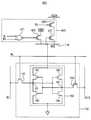
도 1을 참조하면, 본 발명의 일 실시예에 따른 정적 메모리 장치(100)는 비트 셀(130) 및 파워 공급 제어 회로(120)를 포함한다. 상기 파워 공급 제어 회로(120)는 전원 전압(VDDA)과 내부 전압 라인(110) 사이에 연결된다. 상기 파워 공급 제어 회로(120)는 모드 제어 신호(MC)에 따라 비트 셀(130)로 동작 모드에 따라 전압을 공급한다. 도 1의 실시예에서는 모드 제어 신호(MC)가 라이트 어시시트 신호(WA)를 포함할 수 있다.Referring to FIG. 1, a
파워 공급 제어 회로(120)는 제1 피모스 트랜지스터(121) 및 제2 피모스 트랜지스터(123)를 포함할 수 있다. 제1 피모스 트랜지스터(121)는 소스 단자가 전원 전압(VDDA)에 연결되고 드레인은 내부 전압 라인(110)에 연결되고 게이트에는 라이트 어시시트(WA) 신호가 인가된다. 제2 피모스 트랜지스터(123)의 소스는 전원 전 압(VDDA)에 연결되고, 드레인과 게이트는 내부 전압 라인(110)에 연결된다.The power
상기 제1 피모스 트랜지스터(121)의 게이트에 인가되는 라이트 어시스트 신호(WA)가 로우 레벨이면, 제1 피모스 트랜지스터(121)가 턴 온 된다. 따라서 이 때 내부 전압 라인(110)의 전압은 전원 전압(VDDA)이 되고, 비트 셀(130)의 래치 회로(160)에도 전원 전압(VDDA)이 공급된다. 이 때 비트 셀(130)은 읽기 모드로 동작할 수 있다.When the write assist signal WA applied to the gate of the
상기 제1 피모스 트랜지스터(121)의 게이트에 인가되는 라이트 어시스트 신호(WA)가 하이 레벨이면, 제1 피모스 트랜지스터(121)가 턴 오프 된다. 따라서 이 때 내부 전압 라인(110)의 전압 레벨은 플로팅 상태가 되고, 비트 셀(130)의 래치 회로(160)에도 플로팅 상태의 전압이 공급된다. 이 때 비트 셀(130)은 쓰기 모드로 동작할 수 있다. When the write assisting signal WA applied to the gate of the
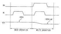
도 7a 라이트 어시시트 신호에 따른 본 발명의 일 실시예에 따른 정적 메모리 장치의 전압 레벨을 나타낸다.Figure 7a shows the voltage level of a static memory device according to an embodiment of the present invention in accordance with a write assertion signal.
도 1 및 도 7a를 참조하면, 비트 셀(130)에 대한 읽기 동작 시 워드 라인(WL)이 인에이블 되고, 라이트 어시시트 신호(WA)가 로우 레벨이면 내부 전압 라인(VDA, 110)의 전압 레벨은 전원 전압(VDDA) 레벨이 된다. 내부 전압 라인(110)이 전원 전압 레벨(VDDA)을 유지하고 있으므로 제1 노드(N1)에 저장된 셀 데이터를 비트 라인(BL)을 통하여 읽을 수 있다. 비트 셀(130)에 대한 쓰기 동작 시에는 워드 라인(WL)이 인에이블 되고, 라이트 어시시트 신호(WA)가 하이 레벨로 천이하면 제1 피모스 트랜지스터(121)가 턴 오프 되고, 제2 피모스 트랜지스터(123)는 게이트와 드레인이 서로 연결되어 있으므로 다이오드처럼 동작하게 된다. 따라서 내부 전압 라인(110)의 전압 레벨은 플로팅하게 된다. 즉 내부 전압 라인(110)은 제1 레벨과 제2 레벨 사이에서 플로팅하게 된다. 여기서 제1 레벨은 전원 전압(VDDA) 레벨일 있고, 제2 레벨은 전원 전압(VDDA)에서 일정한 값(여기서는 제2 피모스 트랜지스터(123)의 문턱 전압값)을 뺀 값에 해당할 수 있다.1 and 7A, the word line WL is enabled during a read operation for the
비트 셀(130)에 대한 쓰기 동작은 제1 노드(N1)와 제2 노드(N2)에 저장된 데이터의 값을 반대로 바꾸는 동작이다. 이 때 제1 피모스 트랜지스터(161) 및 제2 피모스(163)는 제1 노드(N1)와 제2 노드(N2)에 저장된 데이터를 유지하려고 한다. 따라서 제1 피모스 트랜지스터(161)와 제2 피모스 트랜지스터(163)에 공급되는 전압(즉 내부 전압 라인(110)의 전압 레벨, 즉 구동능력)이 제1 및 제2 억세스 트랜지스터들(140, 150)의 구동 능력보다 낮으면 제1 노드(N1)와 제2 노드(N2)에 저장된 데이터가 쉽게 반전될 수 있다. 하지만 제1 피모스 트랜지스터(161)와 제2 피모스 트랜지스터(163)에 공급되는 전압이 너무 낮아지면 리텐션 페일(retention fail)이 발생할 수 있다. 하지만 본 발명의 일 실시예에 따르면 내부 전압 라인(110)의 전압 레벨은 전원 전압(VDDA)과 전원 전압(VDDA)에서 일정한 값(△V)을 뺀 값 사이에서 플로팅하므로 리텐션 페일을 방지하면서 쓰기 동작을 안정적으로 수행할 수 있다. 또한 이러한 라이트 어시시트 기능은 쓰기 동작이 불안정한 셀에서 발생하므로 저전력 구현에도 용이하다.The write operation to the
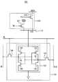
도 2는 본 발명의 일 실시예에 따른 정적 메모리 장치를 나타낸다.Figure 2 shows a static memory device according to an embodiment of the present invention.
도 2의 정적 메모리 장치(200)는 추가적으로 슬립 모드를 구현할 수 있다.The
도 2를 참조하면, 정적 메모리 장치(200)는 비트 셀(130) 및 파워 공급 제어 회로(220)를 포함한다. 상기 파워 공급 제어 회로(220)는 전원 전압(VDDA)과 내부 전압 라인(110) 사이에 연결된다. 상기 파워 공급 제어 회로(220)는 모드 제어 신호(MC)에 따라 비트 셀(130)로 동작 모드에 따라 전압을 공급한다. 도 2의 실시예에서는 모드 제어 신호(MC)가 라이트 어시시트 신호(WA)와 슬립모드 신호(SL)를 포함할 수 있다.Referring to FIG. 2, the
파워 공급 제어 회로(220)는 낸드 게이트(221), 제1 피모스 트랜지스터(223) 및 제2 피모스 트랜지스터(225)를 포함할 수 있다. 낸드 게이트(221)는 슬립 모드 신호(SL)와 라이트 어시시트 신호(WA)를 인가받는다. 제1 피모스 트랜지스터(223)는 소스 단자가 전원 전압(VDDA)에 연결되고 드레인은 내부 전압 라인(110)에 연결되고 게이트에는 낸드 게이트(221)의 출력 신호가 인가된다. 제2 피모스 트랜지스터(225)의 소스는 전원 전압(VDDA)에 연결되고, 드레인과 게이트는 내부 전압 라인(110)에 연결된다.The power
슬립 모드 신호(SL)가 로우 레벨이면 라이트 어시시스 신호(WA)에 상관 없이 비트 셀(130)은 슬립 모드로 동작한다.When the sleep mode signal SL is at a low level, the
슬립 모드 신호(SL)와 라이트 어시시트 신호(WA)가 모두 하이 레벨이면 낸드 게이트(221)의 출력은 로우 레벨이 되고, 제1 피모스 트랜지스터(223)는 턴 온 된다. 따라서 이 때 내부 전압 라인(110)의 전압은 전원 전압(VDDA)이 되고, 비트 셀(130)의 래치 회로(160)에도 전원 전압(VDDA)이 공급된다. 이 때 비트 셀(130)은 읽기 모드로 동작할 수 있다.When both the sleep mode signal SL and the write assertion signal WA are at the high level, the output of the
슬립 모드 신호(SL)가 하이 레벨이고 라이트 어시시트 신호(WA)가 로우 레벨이면 제1 피모스 트랜지스터(223)가 턴 오프 된다. 제2 피모스 트랜지스터(225)는 게이트와 드레인이 서로 연결되어 다이오드처럼 동작한다. 따라서 이 때 내부 전압 라인(110)의 전압 레벨은 플로팅 상태가 되고, 비트 셀(130)의 래치 회로(160)에도 플로팅 상태의 전압이 공급된다. 이 때 비트 셀(130)은 쓰기 모드로 동작할 수 있다.The
도 7b는 라이트 어시시트 신호에 따른 본 발명의 일 실시예에 따른 정적 메모리 장치의 전압 레벨을 나타낸다.7B shows the voltage level of a static memory device according to an embodiment of the present invention in accordance with a write assertion signal.
도 2 및 도 7b를 참조하면, 비트 셀(130)에 대한 읽기 동작 시 워드 라인(WL)이 인에이블 되고, 라이트 어시시트 신호(WA)가 하이 레벨이면 내부 전압 라인(VDA, 110)의 전압 레벨은 전원 전압(VDDA) 레벨이 된다. 내부 전압 라인(110)이 전원 전압 레벨(VDDA)을 유지하고 있으므로 제1 노드(N1)에 저장된 셀 데이터를 비트 라인(BL)을 통하여 읽을 수 있다. 비트 셀(130)에 대한 쓰기 동작 시에는 워드 라인(WL)이 인에이블 되고, 라이트 어시시트 신호(WA)가 하이 레벨로 천이하면 제1 피모스 트랜지스터(223)가 턴 오프 되고, 제2 피모스 트랜지스터(225)는 게이트와 드레인이 서로 연결되어 있으므로 다이오드처럼 동작하게 된다. 따라서 내부 전압 라인(110)의 전압 레벨은 플로팅하게 된다. 즉 내부 전압 라인(110)은 제1 레벨과 제2 레벨 사이에서 플로팅하게 된다. 여기서 제1 레벨은 전원 전압(VDDA) 레벨일 있고, 제2 레벨은 전원 전압(VDDA)에서 일정한 값(여기서는 제2 피모스 트랜지스터(225)의 문턱 전압값)을 뺀 값에 해당할 수 있다. 도 2의 정적 메모리 장치의 동 작은 도 1의 정적 메모리 장치의 동작과 유사하므로 이에 대한 상세한 설명은 생략한다.2 and 7B, the word line WL is enabled during a read operation for the
도 3은 본 발명의 일 실시예에 따른 정적 메모리 장치를 나타낸다.Figure 3 illustrates a static memory device according to one embodiment of the present invention.
도 3의 정적 메모리 장치는 추가적으로 파워 다운 모드를 구현할 수 있다.The static memory device of FIG. 3 may additionally implement a power down mode.
도 3을 참조하면, 정적 메모리 장치(300)는 비트 셀(130) 및 파워 공급 제어 회로(320)를 포함한다. 상기 파워 공급 제어 회로(320)는 전원 전압(VDDA)과 내부 전압 라인(110) 사이에 연결된다. 상기 파워 공급 제어 회로(520)는 모드 제어 신호(MC)에 따라 비트 셀(130)로 동작 모드에 따라 전압을 공급하거나 차단한다. 도 3의 실시예에서는 모드 제어 신호(MC)가 라이트 어시시트 신호(WA)와 파워 다운 신호(PD)를 포함할 수 있다.Referring to FIG. 3, the
파워 공급 제어 회로(320)는 제1 피모스 트랜지스터(321) 제2 피모스 트랜지스터(323) 및 제3 피모스 트랜지스터(325)를 포함할 수 있다. 제1 피모스 트랜지스터(321)는 소스 단자가 전원 전압(VDDA)에 연결되고 드레인은 내부 전압 라인(110)에 연결되고 게이트에는 라이트 어시시트 신호(WA)가 인가된다. 제2 피모스 트랜지스터(323)의 소스는 전원 전압(VDDA)에 연결되고, 게이트에는 파워 다운 신호(PD)가 인가된다. 제3 피모스 트랜지스터(327)의 소스는 제2 피모스 트랜지스터(323)의 드레인에 연결되고 게이트와 드레인은 내부 전압 라인(110)에 연결된다.The power
파워 다운 신호(PD)와 라이트 어시시트 신호(WA)가 모두 하이 레벨이면 제1 피모스 트랜지스터(321)와 제2 피모스 트랜지스터(323)가 턴 오프되어 비트 셀(130)에는 전압 공급이 차단된다. 즉 도 3의 파워 공급 제어 회로(320)는 파워 게이팅 회로로서 동작할 수 있다.The
파워 다운 신호(PD)와 라이트 어시시트 신호(WA)가 모두 로우 레벨이면 제1 피모스 트랜지스터(321)와 제2 피모스 트랜지스터(323)가 턴 온 된다. 따라서 이 때 내부 전압 라인(110)의 전압은 전원 전압(VDDA)이 되고, 비트 셀(130)의 래치 회로(160)에도 전원 전압(VDDA)이 공급된다. 이 때 비트 셀(130)은 읽기 모드로 동작할 수 있다.The
파워 다운 신호(PD)가 로우 레벨이고 라이트 어시시트 신호(WA)가 하이 레벨이면 제1 피모스 트랜지스터(321)는 턴 오프되고, 제2 피모스 트랜지스터(323)는 턴 온 되고, 제3 피모스 트랜지스터(325)는 게이트와 드레인이 서로 연결되어 다이오드처럼 동작한다. 따라서 이 때 내부 전압 라인(110)의 전압 레벨은 플로팅 상태가 되고, 비트 셀(130)의 래치 회로(160)에도 플로팅 상태의 전압이 공급된다. 이 때 비트 셀(130)은 쓰기 모드로 동작할 수 있다.The
도 3의 정적 메모리 장치의 전압 레벨은 도 7a에서 확인할 수 있다. 이 때, 일정한 값(△V)은 제3 피모스 트랜지스터(325)의 문턱 전압 값일 수 있다.The voltage level of the static memory device of Figure 3 can be seen in Figure 7a. At this time, the constant value? V may be the threshold voltage value of the
도 3의 정적 메모리 장치의 동작은 도 1의 정적 메모리 장치의 동작과 유사하므로 이에 대한 상세한 설명은 생략한다.The operation of the static memory device of FIG. 3 is similar to that of the static memory device of FIG. 1, so a detailed description thereof will be omitted.
도 4는 본 발명의 일 실시예에 따른 정적 메모리 장치를 나타낸다.Figure 4 illustrates a static memory device according to one embodiment of the present invention.
도 4의 정적 메모리 장치는 추가적으로 파워 다운 모드와 슬립 모드를 구현할 수 있다.The static memory device of FIG. 4 may further implement a power down mode and a sleep mode.
도 4를 참조하면, 정적 메모리 장치(400)는 비트 셀(130) 및 파워 공급 제어 회로(320)를 포함한다. 상기 파워 공급 제어 회로(320)는 전원 전압(VDDA)과 내부 전압 라인(110) 사이에 연결된다. 상기 파워 공급 제어 회로(220)는 모드 제어 신호(MC)에 따라 비트 셀(130)로 동작 모드에 따라 전압을 공급하거나 차단한다. 도 4의 실시예에서는 모드 제어 신호(MC)는 라이트 어시시트 신호(WA)와 파워 다운 신호(PD)와 슬립 모드 신호(SL)를 포함할 수 있다.Referring to FIG. 4, the
파워 공급 제어 회로(320)는 낸드 게이트(421), 제1 피모스 트랜지스터(423), 제2 피모스 트랜지스터(425) 및 제3 피모스 트랜지스터(427)를 포함할 수 있다. 낸드 게이트(421)는 라이트 어시시트 신호(WA)와 슬립 모드 신호(SL)를 인가받는다. 제1 피모스 트랜지스터(421)는 소스 단자가 전원 전압(VDDA)에 연결되고 드레인은 내부 전압 라인(110)에 연결되고 게이트에는 낸드 게이트(421)의 출력 신호가 인가된다. 제2 피모스 트랜지스터(423)의 소스는 전원 전압(VDDA)에 연결되고, 게이트에는 파워 다운 신호(PD)가 인가된다. 제3 피모스 트랜지스터(427)의 소스는 제2 피모스 트랜지스터(425)의 드레인에 연결되고 게이트와 드레인은 내부 전압 라인(110)에 연결된다.The power
파워 다운 신호(PD)가 하이 레벨이고 슬립 모드 신호(SL)가 하이 레벨이면 라이트 어시시트 신호(WA)에 상관없이 제1 피모스 트랜지스터(423)와 제2 피모스 트랜지스터(425)가 턴 오프되어 비트 셀(130)에는 전압 공급이 차단된다. 즉 도 4의 파워 공급 제어 회로(420)는 파워 게이팅 회로로서 동작할 수 있다.When the power down signal PD is at the high level and the sleep mode signal SL is at the high level, the
파워 다운 신호(PD)가 로우 레벨이고, 슬립 모드 신호(SL)가 하이 레벨이면 라이트 어시스트 신호(WA)에 상관없이 비트 셀(130)은 슬립 모드에서 동작할 수 있 다.When the power-down signal PD is at a low level and the sleep mode signal SL is at a high level, the
파워 다운 신호(PD)가 로우 레벨이고 슬립 모드 신호(SL)가 하이 레벨이고 라이트 어시시트 신호(WA)가 하이 레벨이면 제1 피모스 트랜지스터(423)가 턴 온 된다. 따라서 이 때 내부 전압 라인(110)의 전압은 전원 전압(VDDA)이 되고, 비트 셀(130)의 래치 회로(160)에도 전원 전압(VDDA)이 공급된다. 이 때 비트 셀(130)은 읽기 모드로 동작할 수 있다.The
파워 다운 신호(PD)가 로우 레벨이고 슬립 모드 신호(SL)가 하이 레벨이고, 라이트 어시시트 신호(WA)가 로우 레베이면, 제1 피모스 트랜지스터(423)는 턴 오프되고, 제2 피모스 트랜지스터(425)는 턴 온 되고, 제3 피모스 트랜지스터(325)는 게이트와 드레인이 서로 연결되어 다이오드처럼 동작한다. 따라서 이 때 내부 전압 라인(110)의 전압 레벨은 플로팅 상태가 되고, 비트 셀(130)의 래치 회로(160)에도 플로팅 상태의 전압이 공급된다. 이 때 비트 셀(130)은 쓰기 모드로 동작할 수 있다.When the power down signal PD is at the low level and the sleep mode signal SL is at the high level and the write assertion signal WA is low level, the
도 4의 정적 메모리 장치의 전압 레벨은 도 7b에서 확인할 수 있다. 이 때, 일정한 값(△V)은 제3 피모스 트랜지스터(427)의 문턱 전압 값일 수 있다.The voltage level of the static memory device of Figure 4 can be seen in Figure 7b. At this time, the constant value? V may be the threshold voltage value of the
도 4의 정적 메모리 장치의 동작은 도 3의 정적 메모리 장치의 동작과 유사하므로 이에 대한 상세한 설명은 생략한다.The operation of the static memory device of FIG. 4 is similar to that of the static memory device of FIG. 3, so a detailed description thereof will be omitted.
도 5는 본 발명의 일 실시예에 따른 정적 메모리 장치를 나타낸다.Figure 5 illustrates a static memory device according to one embodiment of the present invention.
도 5의 정적 메모리 장치는 도 3의 정적 메모리 장치와 같이 추가적으로 파워 다운 모드를 구현할 수 있다.The static memory device of FIG. 5 may additionally implement a power down mode like the static memory device of FIG.
도 5를 참조하면, 정적 메모리 장치(500)는 비트 셀(130) 및 파워 공급 제어 회로(520)를 포함한다. 상기 파워 공급 제어 회로(520)는 전원 전압(VDDA)과 내부 전압 라인(110) 사이에 연결된다. 상기 파워 공급 제어 회로(520)는 모드 제어 신호(MC)에 따라 비트 셀(130)로 동작 모드에 따라 전압을 공급하거나 차단한다. 도 5의 실시예에서는 모드 제어 신호(MC)가 라이트 어시시트 신호(WA)와 파워 다운 신호(PD)를 포함할 수 있다. 5, the
파워 공급 제어 회로(520)는 피모스 트랜지스터(521)와 엔모스 트랜지스터(523)를 포함한다. 피모스 트랜지스터(521)는 소스 단자가 전원 전압(VDDA)에 연결되고 드레인은 내부 전압 라인(110)에 연결되고 게이트에는 라이트 어시시트 신호(WA)가 인가된다. 엔모스 트랜지스터(523)의 드레인은 전원 전압(VDDA)에 연결되고, 게이트에는 파워 다운 신호(PD)가 인가되고 소스는 내부 전압 라인(110)에 연결된다.The power
파워 다운 신호(PD)가 로우 레벨이고 라이트 어시스트 신호(WA)가 하이 레벨이면 엔모스 트랜지스터(523)와 피모스 트랜지스터(521)가 모두 턴 오프 되어 비트 셀(130)에는 전압 공급이 차단된다. 즉 도 5의 파워 공급 제어 회로(520)는 파워 게이팅 회로로서 동작할 수 있다.When the power down signal PD is at the low level and the write assisting signal WA is at the high level, both the
파워 다운 신호(PD)가 하이 레벨이고 라이트 어시시트 신호(WA)가 로우 레벨이면 엔모스 트랜지스터(523)와 피모스 트랜지스터(521)가 턴 온 된다. 따라서 이 때 내부 전압 라인(110)의 전압은 전원 전압(VDDA)이 되고, 비트 셀(130)의 래치 회로(160)에도 전원 전압(VDDA)이 공급된다. 이 때 비트 셀(130)은 읽기 모드로 동 작할 수 있다.When the power down signal PD is at a high level and the write assertion signal WA is at a low level, the
라이트 어시시트 신호(WA)가 하이 레벨이고 파워 다운 신호(PD)가 하이 레벨이면 피모스 트랜지스터(521)는 턴 오프 되고, 엔모스 트랜지스터(523)는 턴 온 되어 이 때 내부 전압 라인(110)의 전압 레벨은 플로팅 상태가 되고, 비트 셀(130)의 래치 회로(160)에도 플로팅 상태의 전압이 공급된다. 이 때 비트 셀(130)은 쓰기 모드로 동작할 수 있다. 도 5의 정적 메모리 장치(500)는 도 3의 정적 메모리 장치(300)의 제2 피모스 트랜지스터(323)와 제3 피모스 트랜지스터(325)를 엔모스 트랜지스터(523)로 대체한 것이다.When the write assertion signal WA is at a high level and the power down signal PD is at a high level, the
도 5의 정적 메모리 장치의 전압 레벨은 도 7a에서 확인할 수 있다. 이 때, 일정한 값(△V)은 엔모스 트랜지스터(523)의 문턱 전압 값일 수 있다.The voltage level of the static memory device of Figure 5 can be seen in Figure 7a. At this time, the constant value? V may be the threshold voltage value of the
도 5의 정적 메모리 장치의 동작은 도 3의 정적 메모리 장치의 동작과 유사하므로 이에 대한 상세한 설명은 생략한다.Since the operation of the static memory device of FIG. 5 is similar to that of the static memory device of FIG. 3, a detailed description thereof will be omitted.
도 6은 본 발명의 일 실시예에 따른 정적 메모리 장치를 나타낸다.6 shows a static memory device according to an embodiment of the invention.
도 6의 정적 메모리 장치는 추가적으로 파워 다운 모드와 슬립 모드를 구현할 수 있다.The static memory device of FIG. 6 may additionally implement a power down mode and a sleep mode.
도 6을 참조하면, 정적 메모리 장치(600)는 비트 셀(130) 및 파워 공급 제어 회로(320)를 포함한다. 상기 파워 공급 제어 회로(320)는 전원 전압(VDDA)과 내부 전압 라인(110) 사이에 연결된다. 상기 파워 공급 제어 회로(220)는 모드 제어 신호(MC)에 따라 비트 셀(130)로 동작 모드에 따라 전압을 공급하거나 차단한다. 도 6의 실시예에서는 모드 제어 신호(MC)는 라이트 어시시트 신호(WA)와 파워 다운 신 호(PD)와 슬립 모드 신호(SL)를 포함할 수 있다.Referring to FIG. 6, the
파워 공급 제어 회로(620)는 낸드 게이트(621), 피모스 트랜지스터(623), 및 엔모스 트랜지스터(625)를 포함할 수 있다. 낸드 게이트(621)는 라이트 어시시트 신호(WA)와 슬립 모드 신호(SL)를 인가받는다. 피모스 트랜지스터(623)는 소스 단자가 전원 전압(VDDA)에 연결되고 드레인은 내부 전압 라인(110)에 연결되고 게이트에는 낸드 게이트(621)의 출력 신호가 인가된다. 엔모스 트랜지스터(625)의 드레인 전원 전압(VDDA)에 연결되고, 게이트에는 파워 다운 신호(PD)가 인가되고 소스는 내부 전압 라인(110)에 연결된다.The power
파워 다운 신호(PD)가 하이 레벨이고 슬립 모드 신호(SL)가 로우 레벨이면 라이트 어시시트 신호(WA)에 상관없이 피모스 트랜지스터(523)와 엔모스 트랜지스터(625)가 턴 오프되어 비트 셀(130)에는 전압 공급이 차단된다. 즉 도 6의 파워 공급 제어 회로(620)는 파워 게이팅 회로로서 동작할 수 있다.When the power down signal PD is at the high level and the sleep mode signal SL is at the low level, the
파워 다운 신호(PD)가 하이 레벨이고, 슬립 모드 신호(SL)가 하이 레벨이면 라이트 어시스트 신호(WA)에 상관없이 비트 셀(130)은 슬립 모드에서 동작할 수 있다.When the power down signal PD is at a high level and the sleep mode signal SL is at a high level, the
파워 다운 신호(PD)가 하이 레벨이고 슬립 모드 신호(SL)가 하이 레벨이고 라이트 어시시트 신호(WA)가 하이 레벨이면 피모스 트랜지스터(623)가 턴 온 된다. 따라서 이 때 내부 전압 라인(110)의 전압은 전원 전압(VDDA)이 되고, 비트 셀(130)의 래치 회로(160)에도 전원 전압(VDDA)이 공급된다. 이 때 비트 셀(130)은 읽기 모드로 동작할 수 있다.When the power down signal PD is at the high level, the sleep mode signal SL is at the high level, and the light assyacate signal WA is at the high level, the
파워 다운 신호(PD)가 하이 레벨이고 슬립 모드 신호(SL)가 하이 레벨이고, 라이트 어시시트 신호(WA)가 로우 레벨이면, 피모스 트랜지스터(623)는 턴 오프 되고, 엔모스 트랜지스터(625)는 턴 온 된다. 이 때 내부 전압 라인(110)의 전압 레벨은 플로팅 상태가 되고, 비트 셀(130)의 래치 회로(160)에도 플로팅 상태의 전압이 공급된다. 이 때 비트 셀(130)은 쓰기 모드로 동작할 수 있다. 도 6의 정적 메모리 장치(600)는 도 4의 정적 메모리 장치(400)의 제2 피모스 트랜지스터(425)와 제3 피모스 트랜지스터(427)를 엔모스 트랜지스터(625)로 대체한 것이다.When the power down signal PD is at a high level and the sleep mode signal SL is at a high level and the write assertion signal WA is at a low level, the
도 6의 정적 메모리 장치의 전압 레벨은 도 7b에서 확인할 수 있다. 이 때, 일정한 값(△V)은 엔모스 트랜지스터(625)의 문턱 전압 값일 수 있다.The voltage level of the static memory device of Figure 6 can be seen in Figure 7b. At this time, the constant value? V may be the threshold voltage value of the
도 6의 정적 메모리 장치의 동작은 도 4의 정적 메모리 장치의 동작과 유사하므로 이에 대한 상세한 설명은 생략한다.The operation of the static memory device of FIG. 6 is similar to that of the static memory device of FIG. 4, so a detailed description thereof will be omitted.
도 8a 내지 도 8c는 본 발명의 일 실시예들에 따른 정적 메모리 장치와 종래의 정적 메모리 장치의 시뮬레이션 결과를 나타낸다.Figures 8A-8C show simulation results of a static memory device and a conventional static memory device in accordance with embodiments of the present invention.
도 8a는 전형적으로 안정한 비트 셀을 나타내고 도 8b는 불안정한 셀을 나타내고 도 8c는 본 발명의 실시예들에 따른 정적 메모리 장치의 비트 셀을 나타낸다.FIG. 8A typically shows a stable bit cell, FIG. 8B shows an unstable cell, and FIG. 8C shows a bit cell of a static memory device according to embodiments of the present invention.
도 8a를 참조하면, 안정한 비트 셀에서는 라이트 동작시 워드 라인(WL)이 인에이블 되면 비트 셀(160)의 제1 노드(N1)와 제2 노드(N2)의 전압 레벨들(DATA, DATAB)이 워드 라인(WL)의 전압 레벨과 동일한 레벨로 플립(flip)되는 것을 알 수 있다. 도 8b를 참조하면, 불안정한 비트 셀에서는 라이트 어시스트를 적용하지 않을 경우 워드 라인(WL)이 인에이블 되어도 비트 셀(160)의 제1 노드(N1)와 제2 노 드(N2)의 전압 레벨들(DATA, DATAB)이 플립되지 않는 것을 알 수 있다. 도 8c를 참조하면, 불안정한 비트 셀에서 라이트 어시시트를 적용하는 경우 워드 라인(WL)이 인에이블 되면 비트 셀(160)의 제1 노드(N1)와 제2 노드(N2)의 전압 레벨들(DATA, DATAB)이 워드 라인(WL)의 전압 레벨보다 약간 감소된 레벨에서 플립되는 것을 알 수 있다.Referring to FIG. 8A, in a stable bit cell, when the word line WL is enabled in a write operation, the voltage levels DATA and DATAB of the first node N1 and the second node N2 of the
도 9는 본 발명의 일 실시예에 따른 라이트 어시시트 기능을 구비하는 에스램의 구성을 나타낸다.FIG. 9 shows a configuration of an ESRAM having a write assisite function according to an embodiment of the present invention.
도 9를 참조하면, 라이트 어시시트 기능을 구비하는 에스램(900)는 복수의 워드 라인들(WL1, WL2,...,WLM), 복수의 비트 라인 쌍들(BL1, BLB1,...,BLN, BLBN), 비트 셀 어레이(970), 로우 디코더(950), 칼럼 디코더(920), 칼럼 선택 스위치(910), 쓰기 버퍼(930), 센스 앰프(940) 및 복수의 파워 공급 제어 회로(120)를 포함한다.9, an
각각의 비트 라인쌍들(BL1, BLB1,...,BLN, BLBN)은 복수의 워드 라인들(WL1, WL2,...,WLM)과 교차하고, 비트 라인들(BL1, BL2,..., BLN) 및 비트바 라인들(BLB1, BLB2,...,BLBN)를 구비한다. 로우 디코더(950)는 외부로부터 인가되는 로우 어드레스 신호(XADDR)에 응답하여 복수의 워드 라인들(WL1, WL2,...,WLM)중에 하나의 워드 라인을 선택한다. 칼럼 디코더(920)는 외부로부터 인가되는 칼럼 어드레스 신호(YADDR)에 응답하여 복수의 비트 라인쌍들(BL1, BLB1,...,BLN, BLBN)중에 하나의 비트 라인쌍을 선택하기 위한 열 선택 신호를 발생하여 칼럼 선택 스위치(910)로 출력한다. 칼럼 선택 스위치(910)는 칼럼 선택 신호를 입력 받아 복수의 비트 라인쌍들(BBL1, BLB1,...,BLN, BLBN)중에 하나의 비트 라인쌍을 선택한다. 칼럼 선택 스위치는 복수개의 트랜지스터들로 구성될 수 있다. 쓰기 버퍼(930)는 외부로부터 입력 데이터(DI)를 인가받아 선택된 비트 셀에 대해 라이트 동작시 입력 데이터(DI)를 비트 셀에 기록한다. 센스 앰프(940)는 선택된 비트 셀에 대해 리드 동작시 선택된 셀과 연결된 비트 라인 및 비트바 라인의 전압차를 증폭하여 출력 데이터(DO)를 발생한다. 비트 셀 어레이(960)는 복수개의 비트 셀들(BC)을 구비한다. 각각의 비트 셀들(BC)은 워드 라인들(WL1, WL2,...,WLM) 각각에 접속되고, 각각의 비트 라인들(BL1, BL2,..., BLN) 및 비트바 라인(BLB1, BLB2,...,BLBN)들 사이에 접속되어 셀 데이터를 저장한다. Each of the bit line pairs BL1, BLB1, ..., BLN, BLBN intersects a plurality of word lines WL1, WL2, ..., WLM, and the bit lines BL1, BL2, ., BLN and bit bar lines BLB1, BLB2, ..., BLBN. The
라이트 어시시트 기능을 구비하는 에스램(900)은 하나의 칼럼(960)에 포함되는 비트 셀들(BC)당 하나의 파워 공급 제어 회로(120)를 포함할 수 있다. 상기 파워 공급 제어 회로(120)는 전원 전압(VDDA)과 내부 전압 라인(110) 사이에 연결되어 선택된 비트 셀에 모드 제어 신호(MC)에 따라서 전압을 공급한다. 파워 공급 제어 회로(120)는 제1 피모스 트랜지스터(121)와 제2 피모스 트랜지스터(123)을 포함할 수 있다. 모드 제어 신호는 라이트 어시스트 신호(WA1)일 수 있다. 도 9의 파워 공급 제어 회로(120)에는 도 2내지 도 6의 파워 공급 제어 회로들(220, 320, 420, 520, 620)이 포함될 수 있다. 포함되는 파워 공급 제어 회로들에 따라서 모드 제어 신호(MC)는 라이트 어시스트 신호(WA)와 슬립 모드 신호(SL)와 파워 다운 신호(PD)를 선택적으로 포함할 수 있다.An
라이트 어시스트 신호(WA1)가 하이 레벨이면 , 제1 피모스 트랜지스터(121) 가 턴 오프 된다. 따라서 이 때 내부 전압 라인(110)의 전압 레벨은 플로팅 상태가 되고, 비트 셀(130)의 래치 회로(160)에도 플로팅 상태의 전압이 공급된다. 이 때 비트 셀(130)은 쓰기 모드로 동작할 수 있다. 라이트 어시시트 기능을 구비하는 에스램(900)의 동작은 도 1내지 도 6의 정적 메모리 장치와 유사하므로 이에 대한 상세한 설명은 생략한다.When the write assisting signal WA1 is at a high level, the
본 발명에 따르면, 회로 면적을 많이 차지하지 않고 저전력으로 라이트 어시스트 기능을 안정적으로 구현할 수 있으며 제어 신호에 따라 여러 가지 동작 모드를 구현할 수 있어 기존의 파워 게이팅 회로와의 연계도 용이하므로 저전력 특성 및 쓰기 안정성이 요구되는 최근의 미세 공정 에스램 디지인에 상당한 응용성을 갖을 수 있다.According to the present invention, a light assist function can be stably implemented with a low power consumption without occupying a large circuit area, and various operation modes can be implemented according to a control signal, so that it can be easily connected to a conventional power gating circuit. It can have considerable applicability to the recent microprocessing ESRAM design which requires stability.
상술한 바와 같이, 본 발명의 바람직한 실시예를 참조하여 설명하였지만 해당 기술 분야에서 통상의 지식을 가진 자라면 하기의 특허청구범위에 기재된 본 발명의 사상 및 영역으로부터 벗어나지 않는 범위 내에서 본 발명을 다양하게 수정 및 변경시킬 수 있음을 이해할 수 있을 것이다.Although the preferred embodiments of the present invention have been disclosed for illustrative purposes, those skilled in the art will appreciate that various modifications, additions and substitutions are possible, without departing from the scope and spirit of the invention as disclosed in the accompanying claims. It will be understood that the invention may be modified and varied without departing from the scope of the invention.
도 1은 본 발명의 일 실시예에 따른 정적 메모리 장치를 나타낸다.Figure 1 shows a static memory device according to an embodiment of the invention.
도 2는 본 발명의 일 실시예에 따른 정적 메모리 장치를 나타낸다.Figure 2 shows a static memory device according to an embodiment of the present invention.
도 3은 본 발명의 일 실시예에 따른 정적 메모리 장치를 나타낸다.Figure 3 illustrates a static memory device according to one embodiment of the present invention.
도 4는 본 발명의 일 실시예에 따른 정적 메모리 장치를 나타낸다.Figure 4 illustrates a static memory device according to one embodiment of the present invention.
도 5는 본 발명의 일 실시예에 따른 정적 메모리 장치를 나타낸다.Figure 5 illustrates a static memory device according to one embodiment of the present invention.
도 6은 본 발명의 일 실시예에 따른 정적 메모리 장치를 나타낸다.6 shows a static memory device according to an embodiment of the invention.
도 7a 및 도 7b는 라이트 어시시트 신호에 따른 본 발명의 실시예들에 따른 정적 메모리 장치의 전압 레벨을 나타낸다.Figures 7A and 7B show voltage levels of a static memory device according to embodiments of the present invention in accordance with a write assertion signal.
도 8a 내지 도 8c는 본 발명의 일 실시예들에 따른 정적 메모리 장치와 종래의 정적 메모리 장치의 시뮬레이션 결과를 나타낸다.Figures 8A-8C show simulation results of a static memory device and a conventional static memory device in accordance with embodiments of the present invention.
도 9는 본 발명의 일 실시예에 따른 라이트 어시시트 기능을 구비하는 에스램의 구성을 나타낸다.FIG. 9 shows a configuration of an ESRAM having a write assisite function according to an embodiment of the present invention.
Claims (20)
Translated fromKoreanPriority Applications (2)
| Application Number | Priority Date | Filing Date | Title |
|---|---|---|---|
| KR20080027756AKR101488166B1 (en) | 2008-03-26 | 2008-03-26 | SRAM with static memory device and write assertion function |
| US12/382,858US8018788B2 (en) | 2008-03-26 | 2009-03-25 | Static memory device and static random access memory device |
Applications Claiming Priority (1)
| Application Number | Priority Date | Filing Date | Title |
|---|---|---|---|
| KR20080027756AKR101488166B1 (en) | 2008-03-26 | 2008-03-26 | SRAM with static memory device and write assertion function |
Publications (2)
| Publication Number | Publication Date |
|---|---|
| KR20090102362A KR20090102362A (en) | 2009-09-30 |
| KR101488166B1true KR101488166B1 (en) | 2015-02-02 |
Family
ID=41133136
Family Applications (1)
| Application Number | Title | Priority Date | Filing Date |
|---|---|---|---|
| KR20080027756AActiveKR101488166B1 (en) | 2008-03-26 | 2008-03-26 | SRAM with static memory device and write assertion function |
Country Status (2)
| Country | Link |
|---|---|
| US (1) | US8018788B2 (en) |
| KR (1) | KR101488166B1 (en) |
Cited By (2)
| Publication number | Priority date | Publication date | Assignee | Title |
|---|---|---|---|---|
| US11568924B2 (en) | 2020-10-27 | 2023-01-31 | Samsung Electronics Co., Ltd. | Static random access memory (SRAM) devices and methods of operating the same |
| US11636894B2 (en) | 2020-11-06 | 2023-04-25 | Samsung Electronics Co., Ltd. | Integrated circuit including cell array with write assist cell |
Families Citing this family (21)
| Publication number | Priority date | Publication date | Assignee | Title |
|---|---|---|---|---|
| US7596012B1 (en)* | 2006-12-04 | 2009-09-29 | Marvell International Ltd. | Write-assist and power-down circuit for low power SRAM applications |
| US20090285039A1 (en)* | 2008-05-15 | 2009-11-19 | International Business Machines Corporation | Method and apparatus for locally generating a virtual ground for write assist on column selected sram cells |
| US7817481B2 (en)* | 2008-07-03 | 2010-10-19 | International Business Machines Corporation | Column selectable self-biasing virtual voltages for SRAM write assist |
| US9875788B2 (en)* | 2010-03-25 | 2018-01-23 | Qualcomm Incorporated | Low-power 5T SRAM with improved stability and reduced bitcell size |
| US8659936B2 (en)* | 2010-07-06 | 2014-02-25 | Faraday Technology Corp. | Low power static random access memory |
| US8305827B2 (en)* | 2010-07-13 | 2012-11-06 | Taiwan Semiconductor Manufacturing Company, Ltd. | Dual rail memory |
| TWI431624B (en)* | 2010-08-19 | 2014-03-21 | Faraday Tech Corp | Data-aware dynamic supply random access memory |
| KR101799482B1 (en)* | 2010-12-29 | 2017-11-20 | 삼성전자주식회사 | Static random access memory device including write assist circuit |
| US8559212B2 (en)* | 2011-07-06 | 2013-10-15 | Mediatek Inc. | Memory circuit and word line control circuit |
| US8824230B2 (en) | 2011-09-30 | 2014-09-02 | Qualcomm Incorporated | Method and apparatus of reducing leakage power in multiple port SRAM memory cell |
| US9007815B2 (en) | 2012-01-27 | 2015-04-14 | Taiwan Semiconductor Manufacturing Co., Ltd. | Method and apparatus for switching power in a dual rail memory |
| KR20140000010A (en) | 2012-06-22 | 2014-01-02 | 삼성전자주식회사 | Semiconductor memory device |
| US9030893B2 (en)* | 2013-02-06 | 2015-05-12 | Qualcomm Incorporated | Write driver for write assistance in memory device |
| CN107154271B (en)* | 2016-03-03 | 2020-07-17 | 智原微电子(苏州)有限公司 | Static memory device and static memory cell thereof |
| US9728231B1 (en)* | 2016-05-03 | 2017-08-08 | Taiwan Semiconductor Manufacturing Co., Ltd. | Device and method for data-writing |
| US10163524B2 (en) | 2016-06-22 | 2018-12-25 | Darryl G. Walker | Testing a semiconductor device including a voltage detection circuit and temperature detection circuit that can be used to generate read assist and/or write assist in an SRAM circuit portion and method therefor |
| US10497430B2 (en) | 2016-06-22 | 2019-12-03 | Samsung Electronics Co., Ltd. | Semiconductor devices, circuits and methods for read and/or write assist of an SRAM circuit portion based on power supply voltage detection circuits |
| US9916889B1 (en)* | 2016-12-01 | 2018-03-13 | Intel Corporation | Memory circuitry with row-wise gating capabilities |
| TWI674754B (en)* | 2018-12-28 | 2019-10-11 | 新唐科技股份有限公司 | Data retention circuit |
| US10924112B2 (en)* | 2019-04-11 | 2021-02-16 | Ememory Technology Inc. | Bandgap reference circuit |
| US11972793B2 (en) | 2021-09-15 | 2024-04-30 | Mavagail Technology, LLC | Integrated circuit device including an SRAM portion having end power select circuits |
Citations (1)
| Publication number | Priority date | Publication date | Assignee | Title |
|---|---|---|---|---|
| US20060262628A1 (en)* | 2005-05-23 | 2006-11-23 | Renesas Technology Corp. | Semiconductor memory device |
Family Cites Families (5)
| Publication number | Priority date | Publication date | Assignee | Title |
|---|---|---|---|---|
| KR100451422B1 (en) | 1997-12-31 | 2004-12-17 | 주식회사 하이닉스반도체 | Power consumption reduction circuit, especially including a switch unit for controlling a power line supplied to a memory cell |
| JP2002197867A (en) | 2000-12-28 | 2002-07-12 | Nec Corp | Semiconductor device |
| US7804732B2 (en) | 2004-09-22 | 2010-09-28 | St-Ericsson Sa | Memory control with selective retention |
| TWI259939B (en) | 2004-12-02 | 2006-08-11 | Univ Nat Chiao Tung | A power gating structure with concurrent data retention and intermediate modes |
| US7733687B2 (en)* | 2008-02-20 | 2010-06-08 | Taiwan Semiconductor Manufacturing Company, Ltd. | WAK devices in SRAM cells for improving VCCMIN |
- 2008
- 2008-03-26KRKR20080027756Apatent/KR101488166B1/enactiveActive
- 2009
- 2009-03-25USUS12/382,858patent/US8018788B2/enactiveActive
Patent Citations (1)
| Publication number | Priority date | Publication date | Assignee | Title |
|---|---|---|---|---|
| US20060262628A1 (en)* | 2005-05-23 | 2006-11-23 | Renesas Technology Corp. | Semiconductor memory device |
Cited By (2)
| Publication number | Priority date | Publication date | Assignee | Title |
|---|---|---|---|---|
| US11568924B2 (en) | 2020-10-27 | 2023-01-31 | Samsung Electronics Co., Ltd. | Static random access memory (SRAM) devices and methods of operating the same |
| US11636894B2 (en) | 2020-11-06 | 2023-04-25 | Samsung Electronics Co., Ltd. | Integrated circuit including cell array with write assist cell |
Also Published As
| Publication number | Publication date |
|---|---|
| KR20090102362A (en) | 2009-09-30 |
| US20090251984A1 (en) | 2009-10-08 |
| US8018788B2 (en) | 2011-09-13 |
Similar Documents
| Publication | Publication Date | Title |
|---|---|---|
| KR101488166B1 (en) | SRAM with static memory device and write assertion function | |
| US7826253B2 (en) | Semiconductor memory device and driving method thereof | |
| US7113421B2 (en) | Semiconductor integrated circuit device | |
| JP5054919B2 (en) | Semiconductor integrated circuit device | |
| US20040090818A1 (en) | Design concept for SRAM read margin | |
| US8164938B2 (en) | Semiconductor memory device | |
| KR20080039977A (en) | SRM Cells with Separate Read-Write Circuits | |
| US7430134B2 (en) | Memory cell structure of SRAM | |
| US7259986B2 (en) | Circuits and methods for providing low voltage, high performance register files | |
| US9947389B1 (en) | Single ended memory device | |
| US7679947B2 (en) | Semiconductor devices with source and bulk coupled to separate voltage supplies | |
| JP2005302231A (en) | Static random access memory | |
| JP2009020959A (en) | Semiconductor memory device | |
| US11869581B2 (en) | Compensation word line driver | |
| JP4907117B2 (en) | Semiconductor device | |
| US7684231B2 (en) | Methods and apparatus for low power SRAM based on stored data | |
| KR20090096122A (en) | Read assist circuit and sram including the same | |
| KR101696702B1 (en) | Static random access memory and method for operating the same | |
| US11682453B2 (en) | Word line pulse width control circuit in static random access memory | |
| JP2008065863A (en) | Semiconductor memory device | |
| KR20050119235A (en) | Circuit and method for controlling cell voltage in semiconductor memory device |
Legal Events
| Date | Code | Title | Description |
|---|---|---|---|
| PA0109 | Patent application | Patent event code:PA01091R01D Comment text:Patent Application Patent event date:20080326 | |
| PG1501 | Laying open of application | ||
| A201 | Request for examination | ||
| PA0201 | Request for examination | Patent event code:PA02012R01D Patent event date:20130305 Comment text:Request for Examination of Application Patent event code:PA02011R01I Patent event date:20080326 Comment text:Patent Application | |
| E902 | Notification of reason for refusal | ||
| PE0902 | Notice of grounds for rejection | Comment text:Notification of reason for refusal Patent event date:20140522 Patent event code:PE09021S01D | |
| PE0701 | Decision of registration | Patent event code:PE07011S01D Comment text:Decision to Grant Registration Patent event date:20141031 | |
| GRNT | Written decision to grant | ||
| PR0701 | Registration of establishment | Comment text:Registration of Establishment Patent event date:20150126 Patent event code:PR07011E01D | |
| PR1002 | Payment of registration fee | Payment date:20150126 End annual number:3 Start annual number:1 | |
| PG1601 | Publication of registration | ||
| PR1001 | Payment of annual fee | Payment date:20180102 Start annual number:4 End annual number:4 | |
| PR1001 | Payment of annual fee | Payment date:20181228 Start annual number:5 End annual number:5 | |
| FPAY | Annual fee payment | Payment date:20191226 Year of fee payment:6 | |
| PR1001 | Payment of annual fee | Payment date:20191226 Start annual number:6 End annual number:6 | |
| PR1001 | Payment of annual fee | Payment date:20201230 Start annual number:7 End annual number:7 | |
| PR1001 | Payment of annual fee | Payment date:20211229 Start annual number:8 End annual number:8 | |
| PR1001 | Payment of annual fee | Payment date:20221221 Start annual number:9 End annual number:9 | |
| PR1001 | Payment of annual fee | Payment date:20231226 Start annual number:10 End annual number:10 | |
| PR1001 | Payment of annual fee | Payment date:20241226 Start annual number:11 End annual number:11 |