KR101487591B1 - Mom capacitor - Google Patents
Mom capacitorDownload PDFInfo
- Publication number
- KR101487591B1 KR101487591B1KR20130023054AKR20130023054AKR101487591B1KR 101487591 B1KR101487591 B1KR 101487591B1KR 20130023054 AKR20130023054 AKR 20130023054AKR 20130023054 AKR20130023054 AKR 20130023054AKR 101487591 B1KR101487591 B1KR 101487591B1
- Authority
- KR
- South Korea
- Prior art keywords
- electrode
- conductive lines
- line
- conductive line
- line width
- Prior art date
- Legal status (The legal status is an assumption and is not a legal conclusion. Google has not performed a legal analysis and makes no representation as to the accuracy of the status listed.)
- Expired - Fee Related
Links
Images


Classifications
- H—ELECTRICITY
- H10—SEMICONDUCTOR DEVICES; ELECTRIC SOLID-STATE DEVICES NOT OTHERWISE PROVIDED FOR
- H10D—INORGANIC ELECTRIC SEMICONDUCTOR DEVICES
- H10D1/00—Resistors, capacitors or inductors
- H10D1/60—Capacitors
- H10D1/68—Capacitors having no potential barriers
- H10D1/692—Electrodes
- H10D1/711—Electrodes having non-planar surfaces, e.g. formed by texturisation
- H10D1/714—Electrodes having non-planar surfaces, e.g. formed by texturisation having horizontal extensions
- H—ELECTRICITY
- H01—ELECTRIC ELEMENTS
- H01L—SEMICONDUCTOR DEVICES NOT COVERED BY CLASS H10
- H01L23/00—Details of semiconductor or other solid state devices
- H01L23/52—Arrangements for conducting electric current within the device in operation from one component to another, i.e. interconnections, e.g. wires, lead frames
- H01L23/522—Arrangements for conducting electric current within the device in operation from one component to another, i.e. interconnections, e.g. wires, lead frames including external interconnections consisting of a multilayer structure of conductive and insulating layers inseparably formed on the semiconductor body
- H01L23/5222—Capacitive arrangements or effects of, or between wiring layers
- H01L23/5223—Capacitor integral with wiring layers
- H—ELECTRICITY
- H10—SEMICONDUCTOR DEVICES; ELECTRIC SOLID-STATE DEVICES NOT OTHERWISE PROVIDED FOR
- H10D—INORGANIC ELECTRIC SEMICONDUCTOR DEVICES
- H10D1/00—Resistors, capacitors or inductors
- H10D1/01—Manufacture or treatment
- H10D1/041—Manufacture or treatment of capacitors having no potential barriers
- H10D1/042—Manufacture or treatment of capacitors having no potential barriers using deposition processes to form electrode extensions
- H—ELECTRICITY
- H10—SEMICONDUCTOR DEVICES; ELECTRIC SOLID-STATE DEVICES NOT OTHERWISE PROVIDED FOR
- H10D—INORGANIC ELECTRIC SEMICONDUCTOR DEVICES
- H10D1/00—Resistors, capacitors or inductors
- H10D1/60—Capacitors
- H10D1/68—Capacitors having no potential barriers
- H10D1/692—Electrodes
- H10D1/711—Electrodes having non-planar surfaces, e.g. formed by texturisation
- H10D1/716—Electrodes having non-planar surfaces, e.g. formed by texturisation having vertical extensions
- H—ELECTRICITY
- H01—ELECTRIC ELEMENTS
- H01L—SEMICONDUCTOR DEVICES NOT COVERED BY CLASS H10
- H01L2924/00—Indexing scheme for arrangements or methods for connecting or disconnecting semiconductor or solid-state bodies as covered by H01L24/00
- H01L2924/0001—Technical content checked by a classifier
- H01L2924/0002—Not covered by any one of groups H01L24/00, H01L24/00 and H01L2224/00
Landscapes
- Engineering & Computer Science (AREA)
- Power Engineering (AREA)
- Physics & Mathematics (AREA)
- Condensed Matter Physics & Semiconductors (AREA)
- General Physics & Mathematics (AREA)
- Computer Hardware Design (AREA)
- Microelectronics & Electronic Packaging (AREA)
- Semiconductor Integrated Circuits (AREA)
Abstract
Translated fromKoreanDescription
Translated fromKorean본 발명은 반도체 소자의 제조 방법에 관한 것으로서, 특히 반도체 기판상의 커패시터를 이루는 상부 전극과 하부 전극에 연결되는 도전성 라인의 선폭을 변경하여 동일한 면적의 종래 MOM 구조의 커패시터보다 안정적인 커패시턴스를 확보할 수 있는 MOM 커패시터에 관한 것이다.The present invention relates to a method of manufacturing a semiconductor device, and more particularly, to a method of manufacturing a semiconductor device, in which a line width of a conductive line connected to an upper electrode and a lower electrode constituting a capacitor on a semiconductor substrate can be changed to secure a more stable capacitance than a conventional MOM- MOM < / RTI > capacitors.
통상적으로, 반도체 소자의 로직 회로에서 사용되는 커패시터는 MOM과 MIM이 주로 사용되고 있으며, 이러한 커패시터는 MOS형 커패시터나 정션 커패시터와는 달리 바이어스에 독립적이므로 정밀성이 요구된다. MIM 구조의 커패시터는 유효면적 대비 커패시터의 값이 작고, 공정상 마스크가 추가되어 공정 비용이 증가하는 단점이 있어, 이를 보완하기 위해 기존의 BEOL 공정을 이용하여 메탈을 적층하는 MOM 커패시터 구조가 주로 사용되고 있다. MOM 커패시터는 0.13㎛ 이하의 소자설계에 있어서 MIM 커패시터에 비해 더욱 작은 크기로 형성할 수 있어 단위면적당 커패시터의 용량을 크게 확보할 수 있으며, 높은 항복전압을 유지할 수 있는 장점이 있다.Generally, MOM and MIM are mainly used as capacitors used in logic circuits of semiconductor devices. Unlike MOS capacitors and junction capacitors, these capacitors are independent of bias, and therefore precision is required. The capacitor of the MIM structure has a disadvantage that the capacitor value is small relative to the effective area and the process cost is increased due to the addition of a mask in the process. To overcome this, a MOM capacitor structure for laminating metal using the existing BEOL process is mainly used have. The MOM capacitor can be formed in a size smaller than that of the MIM capacitor in a device design of 0.13 μm or less, thereby ensuring a large capacity of the capacitor per unit area and maintaining a high breakdown voltage.
이하, 첨부된 도면을 참고로 종래의 MOM 커패시터의 구조에 대해 설명하면 다음과 같다. 종래의 MOM 커패시터는 통상적으로 상부의 도전성 라인들과 하부의 도전성 라인들이 평행하도록 형성된 평행 구조와, 수직하게 형성된 수직 구조로 나뉘어진다Hereinafter, the structure of a conventional MOM capacitor will be described with reference to the accompanying drawings. Conventional MOM capacitors are typically divided into a parallel structure in which the upper conductive lines and the lower conductive lines are formed in parallel and a vertical structure formed in the vertical direction
도 1a 및 도 1b는 평행 구조로 형성된 MOM 커패시터의 평면도 및 사시도를 나타낸 것이다. 우선 도 1a를 참조하면, MOM 커패시터는 제1 전극(10)에 연결되며, 동일한 선폭을 가지면서 서로 평행하게 형성된 제1 도전성 라인들(11a, 11b, 11c) 및 제2 전극(20)에 연결되며 동일한 선폭을 가지면서 서로 평행하게 형성된 제2 도전성 라인들(21a, 21b, 21c)을 포함한다. 상기 제1 및 제2 도전성 라인들은 동일한 선폭을 가지면서, 제1 및 제2 도전성 라인간의 스페이스 선폭 역시 동일하게 형성된다.1A and 1B are a plan view and a perspective view of a MOM capacitor formed in a parallel structure. 1A, the MOM capacitor is connected to the
그리고, 제1 전극(10) 하부에는 제1 전극(10)과 같은 극의 전위가 인가되는 제3 전극(30)이 형성되며, 제2 전극(20) 하부에는 제2 전극(20)과 같은 극의 전위가 인가되는 제4 전극(40)이 형성된다.A
이러한 구조를 도 1b를 참조하여 살펴보면, 제1 및 제2 도전성 라인들(11, 21)은 하부의 제3 및 제4 도전성 라인들과 반대의 극성을 가지며, 각각의 도전성 라인들의 같은 극성은 교차하도록 형성되어 있다. 제1 및 제2 전극(10, 20)과 제3 및 제4 전극(30, 40) 사이에는 산화막(미도시)이 형성되어, 각각의 도전성 라인들이 평행하게 얼라인되는 구조의 MOM 커패시터를 형성하게 된다. 그러나, 이러한 MOM 커패시터 구조는 단위 면적당 커패시턴스를 높게 확보할 수 있으나, 공정상 미스얼라인(misalign)이 발생하여 도전성 라인간의 스페이스 선폭이 달라질 경우에는 커패시턴스가 크게 낮아지는 문제점이 있다.1B, the first and second conductive lines 11 and 21 have opposite polarities to the third and fourth conductive lines below, and the same polarity of each conductive line is crossed . An oxide film (not shown) is formed between the first and
도 2a 및 도 2b는 수직구조로 형성된 MOM 커패시터의 평면도 및 사시도를 나타낸 것이다. 우선 도 2a를 참조하면, 상부에 위치하는 제1 및 제2 도전성 라인(11, 21)들은 하부의 제3 및 제4 도전성 라인들과 수직방향으로 형성된다. 이러한 MOM 커패시터 구조는 공정상 미스얼라인(misalign)이 발생하여 도전성 라인간의 스페이스 선폭이 달라질 경우에도 일정한 커패시턴스를 유지할 수 있는 장점이 있으나, 단위면적당 커패시턴스가 평행 구조의 커패시터에 비해 작은 문제점이 있다.2A and 2B are a plan view and a perspective view of a MOM capacitor formed in a vertical structure. First, referring to FIG. 2A, the first and second conductive lines 11 and 21 located at the upper portion are formed in a direction perpendicular to the third and fourth conductive lines at the bottom. Such a MOM capacitor structure is advantageous in that a constant capacitance can be maintained even when a space line width between conductive lines changes due to misalignment in the process, but the capacitance per unit area is smaller than that of a parallel structure capacitor.
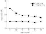
도 3은 종래의 평행 구조 및 수직 구조의 MOM 커패시터에서 미스얼라인이 발생한 경우 커패시턴스의 변화를 나타낸 그래프이다. 도 3을 참조하면, 수직 구조의 MOM 커패시터는 미스얼라인이 발생하여도 일정한 커패시턴스를 유지하지만, 단위면적당 커패시턴스의 값이 상대적으로 작은 것을 확인할 수 있으며, 평행 구조의 MOM 커패시터는 공정상 미스얼라인이 발생되는 경우 커패시턴스가 큰 폭으로 감소함을 확인할 수 있다.FIG. 3 is a graph showing a change in capacitance when misalignment occurs in a conventional MOM capacitor having a parallel structure and a vertical structure. Referring to FIG. 3, it can be seen that the vertical MOM capacitor maintains a constant capacitance even if misalignment occurs. However, it can be seen that the capacitance per unit area is relatively small, and the MOM capacitor of the parallel structure, It can be confirmed that the capacitance is greatly reduced.
상술한 문제점을 해결하기 위하여, MOM 커패시터를 형성함에 있어서 단위 면적당 커패시턴스는 기존과 유사한 값을 확보할 수 있으며, 공정상 미스얼라인이 발생하여도 일정한 커패시턴스를 유지할 수 있는 MOM 커패시터 형성 방법을 제공하는 데에 그 목적이 있다.In order to solve the above-described problems, a method of forming a MOM capacitor capable of maintaining a constant capacitance per unit area in forming a MOM capacitor and maintaining a constant capacitance even if misalignment occurs in the process It has its purpose.
본 발명에 따른 반도체 소자의 커패시터는, 복수개의 평행한 하부 도전성 라인들; 및 상기 하부 도전성 라인들 상부에 형성되는 복수개의 상부 도전성 라인들; 을 포함하여 이루어지고, 상기 하부 도전성 라인 및 상부 도전성 라인들 각각은 인접한 상기 하부 도전성 라인 및 상부 도전성 라인과 서로 다른 선폭을 갖는 것을 특징으로 한다.A capacitor of a semiconductor device according to the present invention comprises: a plurality of parallel lower conductive lines; And a plurality of upper conductive lines formed on the lower conductive lines; And each of the lower conductive line and the upper conductive lines has a different line width from the adjacent lower conductive line and the upper conductive line.
본발명의 실시예에 따르면, 반도체 기판 상의 MOM 커패시터의 도전성 라인의 선폭과 스페이스를 변경함으로써 반도체 소자 제조 공정간 미스얼라인이 발생하는 경우에도 일정한 커패시턴스를 얻을 수 있어 반도체 소자의 안정성이 확보되는 장점이 있다.According to the embodiment of the present invention, by changing the line width and the space of the conductive line of the MOM capacitor on the semiconductor substrate, it is possible to obtain a constant capacitance even when misalignment occurs between semiconductor device manufacturing processes, .
또한, 종래의 MOM 커패시터와 비교하여 단위면적당 커패시턴스를 유사한 수준으로 확보할 수 있어, 고속 및 고주파 동작에 적합한 반도체 소자를 제조하는데 유리한 장점이 있다.In addition, compared to conventional MOM capacitors, the capacitance per unit area can be maintained at a similar level, which is advantageous for manufacturing a semiconductor device suitable for high-speed and high-frequency operation.
도 1a는 종래의 평행 구조로 형성된 MOM 커패시터의 평면도를 나타낸 도면.
도 1b는 종래의 평행 구조로 형성된 MOM 커패시터의 사시도를 나타낸 도면.
도 2a는 종래의 수직 구조로 형성된 MOM 커패시터의 평면도를 나타낸 도면.
도 2b는 종래의 수직 구조로 형성된 MOM 커패시터의 사시도를 나타낸 도면.
도 3은 종래의 평행 구조 및 수직 구조의 MOM 커패시터에서 미스얼라인이 발생한 경우 커패시턴스의 변화를 나타낸 그래프
도 4a는 본발명의 실시예에 따른 MOM 커패시터의 사시도를 나타낸 도면.
도 4b는 본발명의 실시예에 따른 MOM 커패시터의 평면도를 나타낸 도면.
도 5a는 도 4a의 A 영역을 확대하여 종래의 커패시터와 비교한 도면.
도 5b는 도 4a의 A 영역의 상부 및 하부 전극을 나타낸 평면도.
도 5c는 도 5a를 측면에서 바라본 도면.
도 6a는 본발명의 실시예에 따른 MOM 커패시터의 커패시턴스를 측정한 그래프.
도 6b는 본발명의 실시예에 따른 MOM 커패시터에 미스얼라인이 발생한 경우 커패시턴스의 변화를 나타낸 그래프.1A is a plan view of a conventional MOM capacitor formed in a parallel structure.
1B is a perspective view of a conventional MOM capacitor formed in a parallel structure.
2A shows a top view of a conventional MOM capacitor formed in a vertical structure;
2B is a perspective view of a conventional vertical structure MOM capacitor.
FIG. 3 is a graph showing a change in capacitance when misalignment occurs in a conventional MOM capacitor having a parallel structure and a vertical structure
4A is a perspective view of a MOM capacitor according to an embodiment of the present invention.
4B is a top view of a MOM capacitor according to an embodiment of the present invention.
FIG. 5A is an enlarged view of the area A of FIG. 4A and comparing it with a conventional capacitor. FIG.
FIG. 5B is a plan view of the upper and lower electrodes of the region A of FIG. 4A. FIG.
Figure 5c is a side view of Figure 5a.
6A is a graph illustrating a capacitance of a MOM capacitor according to an embodiment of the present invention.
FIG. 6B is a graph showing a change in capacitance when misalignment occurs in the MOM capacitor according to the embodiment of the present invention. FIG.
이하에서는, 본실시예에 대하여 첨부되는 도면을 참조하여 상세하게 살펴보도록 한다. 다만, 본실시예가 개시하는 사항으로부터 본실시예가 갖는 발명의 사항의 범위가 정해질 수 있을 것이며, 본실시예가 갖는 발명의 사상은 제안되는 실시예에 대하여 구성요소의 추가, 삭제, 변경 등의 실시변형을 포함한다고 할 것이다.Hereinafter, the present embodiment will be described in detail with reference to the accompanying drawings. However, the scope of the present invention may be determined from the matters disclosed in the present embodiment, and the spirit of the present invention of the present embodiment is not limited to the embodiments of the present invention, Variations.
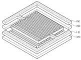
도 4a 및 도 4b는 본발명의 실시예에 따른 MOM 커패시터의 사시도 및 평면도를 나타낸 도면이다.4A and 4B are a perspective view and a plan view of a MOM capacitor according to an embodiment of the present invention.
우선, 도 4a를 참조하면, MOM 커패시터는 상부 전극인 제1 전극(100) 및 제2 전극(110), 그리고 하부 전극인 제3 전극(200) 및 제4 전극(210)을 포함한다. 제1 전극(100) 하부에는 제3 전극(200)이 수직 방향으로 적층되고, 제2 전극(110) 하부에는 제4 전극(210)이 수직 방향으로 적층된다. 상기 제1 전극(100) 및 제3 전극(200)에는 같은 극의 전위가 인가되고, 상기 제2 전극(110) 및 제4 전극(210)에는 같은 극의 전위가 인가되어 단위 구조의 커패시터를 형성한다.Referring to FIG. 4A, the MOM capacitor includes a
도 4b를 참조하면 종래의 평행 구조의 커패시터와 같이, 제1 전극(100)의 일측은 복수개의 제1 상부 도전성 라인들(101a, 101b, 101c)과 연결되며 제2 전극(110)의 일측은 복수개의 제2 상부 도전성 라인들(111a, 111b, 111c)과 연결된다. 상기 제1 전극(100)의 제1 상부 도전성 라인들과 제2 전극(110)의 제2 상부 도전성 라인은 수직 방향으로 적층되어, 하부의 제3 전극(110) 및 제4 전극(210)의 제1 하부 도전성 라인들(201a, 201b, 201c) 및 제2 하부 도전성 라인들(211a, 211b, 211c)과 소정의 폭을 가지면서 얼라인되어 MOM 커패시터를 형성하게 된다.Referring to FIG. 4B, one end of the
각각의 전극에 연결된 각각의 도전성 라인들은 인접한 도전성 라인과 다른 극의 전위가 인가된다. 따라서, 제1 전극(100)은 제2 및 제4 전극(110, 210)과 다른 극의 전위가 인가되며, 제2 전극(110)은 제1 및 제3 전극(100, 200)과 다른 극의 전위가 인가될 수 있다.Each conductive line connected to each electrode is applied with a potential of a different polarity from the adjacent conductive line. Accordingly, the
도 5a는 도 4b의 A 영역을 확대하여 종래 도 1a의 평행 구조의 MOM 커패시터와 비교한 도면이다.FIG. 5A is an enlarged view of the area A of FIG. 4B and compared with the conventional MOM capacitor of FIG. 1A.
도 5a를 참조하여 본발명의 MOM 커패시터의 구조를 상세히 살펴보면, 종래 MOM 커패시터의 인접하는 도전성 라인들(21a, 11a, 21b)은 W의 선폭을 가지며 소정의 거리만큼 이격되고, 서로 다른 전위가 인가되어 커패시턴스를 형성한다.5A, the adjacent
본발명의 A 영역에 위치하는 도전성 라인들과 종래의 A 영역에 대응하는 위치의 도전성 라인들(21a, 11a, 21b)과 비교하면, 상부 전극인 제1 및 제2 전극과 연결되는 제1 및 제2 상부 도전성 라인들(111a, 101a, 111b)의 선폭은 종래의 MOM 커패시터의 도전성 라인의 선폭인 W보다 양측으로 △W 만큼 커지거나 줄어든 도전성 라인들이 교번하여 배치되도록 형성될 수 있다.Compared with the conductive lines located in the A region of the present invention and the
도면에서는 A 영역만을 확대하여 3개의 도전성 라인만을 개시하였으나, 제1 전극(100)은 선폭이 양측으로 △W 만큼 커진 W2의 선폭을 갖는 도전성 라인들이 연속적으로 배치될 수 있으며, 제2 전극(110)은 선폭이 양측으로 △W 만큼 작아진 W1의 선폭을 갖는 도전성 라인들이 연속으로 배치될 수 있다.In the drawing, only the A region is enlarged to disclose only three conductive lines. However, the
상기 제1 전극(100)의 도전성 라인들과, 상기 제1 전극과 다른 전위를 갖는 제2 전극(110)의 도전성 라인들이 교차하도록 배치됨으로써, 인접하는 도전성 라인의 선폭은 상기와 같이 상이하도록 형성된다.The conductive lines of the
도 5b는 도 4b의 A 영역의 상부 및 하부 전극을 나타낸 평면도이다. 도 5b를 참조하면, 제1 전극(100)과 상기 제1 전극(100) 하부에 수직방향으로 적층된 제3 전극(200)을 위에서 바라본 도면이다.And FIG. 5B is a plan view showing upper and lower electrodes of the region A of FIG. 4B. 5B is a top view of a
제3 및 제4 전극은 반도체 기판 상부에 형성되는 하부 전극일 수 있으며, 제1 및 제2 전극은 상기 하부 전극 상에 형성되는 상부 전극일 수 있다. 제1 및 제2 전극(100, 110)의 도전성 라인들(111a, 101a, 111b)과 제3 및 제4 전극(200, 210)의 도전성 라인들(201a, 211a, 201b)은 상하 방향, 좌우 방향으로 선폭이 서로 다른 도전성 라인들이 배치되어 MOM 커패시터를 형성한다. 즉, 하나의 도전성 라인과 인접하는 도전성 라인은 선폭이 크거나 작으면서, 서로 다른 전위가 인가된 도전형 라인으로 형성된다.The third and fourth electrodes may be a lower electrode formed on the semiconductor substrate, and the first and second electrodes may be upper electrodes formed on the lower electrode. The
도 5c는 도 5a를 측면에서 바라본 도면이며, (a)는 종래의 구조를 (b)는 본 발명의 실시예를 나타낸 것이다. 발명의 이해를 돕기 위해, 도전성 라인은 4개를 예로 들어 도시하였다.FIG. 5C is a side view of FIG. 5A. FIG. 5A shows a conventional structure, and FIG. 5B shows an embodiment of the present invention. In order to facilitate understanding of the invention, four conductive lines are shown as an example.
도 5c를 참조하면, 종래의 구조인 (a)에서는 서로 같은 선폭을 가지는 도전성 라인들이 같은 선폭을 가지고 상, 하부간의 커패시턴스를 형성한다.Referring to FIG. 5C, in the conventional structure (a), the conductive lines having the same line width have the same line width and form the capacitance between the upper and lower portions.
그러나 본 발명인 (b)에 도시된 바와 같이, 상부 도전성 라인의 선폭이 소정의 길이만큼 증가하면 하부 도전성 라인의 선폭은 상기 소정의 길이만큼 감소하여 형성된다. 마찬가지로, 상부 도전성 라인의 선폭이 소정의 길이만큼 감소하면 하부 도전성 라인의 선폭은 상기 소정의 길이만큼 증가하여 형성된다. 따라서, 종래의 상부 및 하부의 도전성 라인과 같은 갯수의 상부 및 하부 도전성 라인을 형성하므로, 종래의 커패시터와 유사한 커패시턴스를 유지할 수 있다.However, as shown in (b) of the present invention, when the line width of the upper conductive line is increased by a predetermined length, the line width of the lower conductive line is reduced by the predetermined length. Similarly, when the line width of the upper conductive line is reduced by a predetermined length, the line width of the lower conductive line is increased by the predetermined length. Thus, it forms a number of upper and lower conductive lines, such as conventional upper and lower conductive lines, so that a capacitance similar to that of conventional capacitors can be maintained.
즉, 상기 제1 전극(100)에 연결되는 도전성 라인들은 제3 전극(200)의 도전성 라인들과 수직 방향으로 얼라인되어 커패시턴스를 형성하게 된다. 이 때, 상기 제1 전극(100)과 제3 전극(200)이 수평 방향으로 미스얼라인이 발생하여도 상기 제1 전극(100)의 도전성 라인들과 제3 전극(200)의 도전성 라인들의 선폭이 다르기 때문에 일정한 커패시턴스를 유지할 수 있다.That is, the conductive lines connected to the
마찬가지로, 상기 제2 전극(110)에 연결되는 도전성 라인들은 제4 전극(210)의 도전성 라인들과 수직 방향으로 얼라인되어 커패시턴스를 형성하게 된다. 이 때, 상기 제2 전극(110)과 제4 전극(210)이 수평 방향으로 미스얼라인이 발생하여도 상기 제2 전극(110)의 도전성 라인들과 제4 전극(210)의 도전성 라인들의 선폭이 다르기 때문에 일정한 커패시턴스를 유지할 수 있다.Similarly, the conductive lines connected to the
상기와 같이 형성된 본발명의 MOM 커패시터는 0.18㎛의 테크놀로지에서 △W의 값은 예를 들어 약 100㎚로 설정될 수 있다. 이 때, 종래의 도전성 라인에 비해 줄어든 도전성 라인의 선폭(W1)은 W-200㎚가 되며, 늘어난 도전성 라인의 선폭(W2)은 W+200㎚정도로 형성된다.In the MOM capacitor of the present invention formed as described above, the value of DELTA W in the technology of 0.18 mu m can be set to, for example, about 100 nm. At this time, the line width W1 of the conductive line which is reduced compared to the conventional conductive line becomes W-200 nm, and the line width W2 of the extended conductive line is formed to be about W + 200 nm.
추가로, 0.13㎛의 테크놀로지에서 △W의 값은 약 60㎚로 설정될 수 있다. 이 때, 종래의 도전성 라인에 비해 줄어든 도전성 라인의 선폭(W1)은 W-120㎚ 가 되며, 늘어난 도전성 라인의 선폭(W2)은 W+120㎚정도로 형성된다.In addition, in a 0.13 탆 technology, the value of DELTA W can be set to about 60 nm. At this time, the line width W1 of the conductive line which is reduced compared to the conventional conductive line becomes W-120 nm, and the line width W2 of the extended conductive line is formed to be about W + 120 nm.
도 6a는 본발명의 실시예에 따른 MOM 커패시터의 커패시턴스를 측정한 그래프이다. 도 6a를 참조하면, 대략 5~15 GHz의 고주파 동작을 수행하는 회로에서 측정한 본발명 커패시턴스는 약 4.5E-14 F 값을 유지하는 것을 확인할 수 있으며, 이는 종래 평행 구조의 커패시터가 갖는 단위면적의 커패시턴스와 유사한 수준을 가진다.6A is a graph illustrating a capacitance of a MOM capacitor according to an embodiment of the present invention. Referring to FIG. 6A, it can be seen that the capacitance according to the present invention measured in a circuit performing a high-frequency operation of about 5 to 15 GHz maintains a value of about 4.5E-14F. This is because the unit area Which is similar to the capacitance of the capacitor.
도 6b는 본발명의 실시예에 따른 MOM 커패시터에 미스얼라인이 발생한 경우 커패시턴스의 변화를 나타낸 그래프이다.6B is a graph illustrating a change in capacitance when misalignment occurs in the MOM capacitor according to the embodiment of the present invention.
도 6b를 참조하면, MOM 커패시터는 미스얼라인이 40nm 이하의 수준으로 발생한 경우에는 커패시턴스가 일정한 값을 유지하다가, 미스얼라인이 40nm를 초과하는 경우 커패시턴스가 일정수준 감소하는 것을 확인할 수 있다.Referring to FIG. 6B, it can be seen that the MIS capacitor maintains a constant capacitance when the misalignment occurs at a level of 40 nm or less, and the capacitance decreases when the misalignment exceeds 40 nm.
따라서, 종래 구조에서 미스얼라인이 발생하면 커패시턴스가 급격히 감소하는 것과 비교하여, 본발명에 따른 MOM 커패시터는 공정상 미스얼라인이 발생하여도 일정한 커패시턴스를 확보할 수 있다 즉, 커패시터의 상부 및 하부 전극을 얼라인먼트하는 공정상의 마진을 40nm 까지 확보하여 안정적인 반도체 소자의 제조가 가능하게 된다.Therefore, compared with the case where misalignment occurs in the conventional structure, the capacitance of the MOM capacitor according to the present invention can be kept constant even if misalignment occurs in the process. That is, It is possible to secure a margin of 40 nm in the step of aligning the electrodes, thereby making it possible to manufacture a stable semiconductor device.
또한, 종래의 MOM 커패시터와 비교하여 단위면적당 커패시턴스를 유사한 수준으로 확보할 수 있어, 고속 및 고주파 동작에 적합한 반도체 소자를 제조하는데 유리한 장점이 있다.In addition, compared to conventional MOM capacitors, the capacitance per unit area can be maintained at a similar level, which is advantageous for manufacturing a semiconductor device suitable for high-speed and high-frequency operation.
본 발명의 사상은 상기되는 실시예로 제한되지 아니하며, 본 발명의 사상을 이해하는 당업자는 동일한 사상의 범위내에 포함되는 다른 실시예를 구성요소의 부가, 변경, 삭제 및 추가 등에 의해서 용이하게 제안할 수 있을 것이나, 이 또한 본 발명의 사상에 포함된다고 할 것이다.
It will be understood by those skilled in the art that various changes in form and details may be made therein without departing from the spirit and scope of the invention as defined in the appended claims. It will be appreciated that this is also included in the scope of the present invention.
Claims (13)
Translated fromKorean상기 하부 도전성 라인들 상부에 형성되는 복수개의 상부 도전성 라인들; 을 포함하여 이루어지고,
상기 하부 도전성 라인 및 상부 도전성 라인 각각은 인접한 상기 하부 도전성 라인 및 상부 도전성 라인과 서로 다른 선폭을 갖는 것을 특징으로 하고,
상기 복수개의 평행한 상부 도전성 라인들은,
제1 전극에 연결되어 있는 제1 상부 도전성 라인 및
제2 전극에 연결되어 있는 제2 상부 도전성 라인을 포함하여 이루어지는 것을 특징으로 하고,
상기 제1 상부 도전성 라인의 선폭이 상기 제2 상부 도전성 라인의 선폭보다 넓은 반도체 소자의 커패시터.A plurality of parallel lower conductive lines; And
A plurality of upper conductive lines formed on the lower conductive lines; , ≪ / RTI >
Each of the lower conductive line and the upper conductive line has a different line width from the adjacent lower conductive line and the upper conductive line,
Wherein the plurality of parallel top conductive lines comprise a plurality of parallel top conductive lines,
A first upper conductive line connected to the first electrode,
And a second upper conductive line connected to the second electrode,
And the line width of the first upper conductive line is larger than the line width of the second upper conductive line.
상기 제1 상부 도전성 라인과 제2 상부 도전성 라인은 교번하여 형성되는 것을 특징으로 하는 반도체 소자의 커패시터.The method according to claim 1,
Wherein the first upper conductive line and the second upper conductive line are alternately formed.
상기 제1 상부 도전성 라인과 상기 제2 상부 도전성 라인간의 간격은 일정한 것을 특징으로 하는 반도체 소자의 커패시터.The method according to claim 1,
Wherein a gap between the first upper conductive line and the second upper conductive line is constant.
상기 제1 상부 도전성 라인은 서로 같은 선폭을 갖고, 상기 제2 상부 도전성 라인은 서로 같은 선폭을 갖는 것을 특징으로 하는 반도체 소자의 커패시터.The method according to claim 1,
Wherein the first upper conductive lines have the same line width and the second upper conductive lines have the same line width.
상기 복수개의 평행한 하부 도전성 라인들은,
제3 전극에 연결되어 있는 제1 하부 도전성 라인 및
제4 전극에 연결되어 있는 제2 하부 도전성 라인을 포함하여 이루어지는 것을 특징으로 하는 반도체 소자의 커패시터.The method according to claim 1,
The plurality of parallel lower conductive lines may include a plurality of parallel conductive lines,
A first lower conductive line connected to the third electrode and
And a second lower conductive line connected to the fourth electrode.
상기 제1 하부 도전성 라인들과 제2 하부 도전성 라인들은 교번하여 형성되는 것을 특징으로 하는 반도체 소자의 커패시터.The method according to claim 6,
Wherein the first lower conductive lines and the second lower conductive lines are alternately formed.
상기 제3 전극에 연결되어 있는 제1 하부 도전성 라인은 제2 전극에 연결되어 있는 제2 상부 도전성 라인과 수직방향으로 인접하는 것을 특징으로 하고,
상기 제1 하부 도전성 라인의 선폭은 상기 제2 상부 도전성 라인의 선폭보다 넓고,
상기 제1 상부 도전성 라인의 선폭은 상기 제2 하부 도전성 라인의 선폭보다 넓은 반도체 소자의 커패시터.The method according to claim 6,
The first lower conductive line connected to the third electrode is vertically adjacent to the second upper conductive line connected to the second electrode,
The line width of the first lower conductive line is wider than the line width of the second upper conductive line,
And the line width of the first upper conductive line is larger than the line width of the second lower conductive line.
상기 제3 전극에 연결되어 있는 제1 하부 도전성 라인은
상기 제1 전극에 연결되어 있는 제1 상부 도전성 라인과 같은 선폭을 갖는 것을 특징으로 하는 반도체 소자의 커패시터.The method according to claim 6,
The first lower conductive line connected to the third electrode
And a line width equal to that of the first upper conductive line connected to the first electrode.
상기 제1 전극 및 제3 전극에는 같은 극의 전위가 인가되는 것을 특징으로 하는 반도체 소자의 커패시터.10. The method of claim 9,
And a potential of the same polarity is applied to the first electrode and the third electrode.
상기 하부 도전성 라인과 상부 도전성 라인은 서로 평행한 것을 특징으로 하는 반도체 소자의 커패시터.The method according to claim 1,
Wherein the lower conductive line and the upper conductive line are parallel to each other.
Priority Applications (2)
| Application Number | Priority Date | Filing Date | Title |
|---|---|---|---|
| KR20130023054AKR101487591B1 (en) | 2013-03-04 | 2013-03-04 | Mom capacitor |
| US13/802,997US20140246754A1 (en) | 2013-03-04 | 2013-03-14 | Metal-oxide-metal capacitor |
Applications Claiming Priority (1)
| Application Number | Priority Date | Filing Date | Title |
|---|---|---|---|
| KR20130023054AKR101487591B1 (en) | 2013-03-04 | 2013-03-04 | Mom capacitor |
Publications (2)
| Publication Number | Publication Date |
|---|---|
| KR20140109001A KR20140109001A (en) | 2014-09-15 |
| KR101487591B1true KR101487591B1 (en) | 2015-01-29 |
Family
ID=51420575
Family Applications (1)
| Application Number | Title | Priority Date | Filing Date |
|---|---|---|---|
| KR20130023054AExpired - Fee RelatedKR101487591B1 (en) | 2013-03-04 | 2013-03-04 | Mom capacitor |
Country Status (2)
| Country | Link |
|---|---|
| US (1) | US20140246754A1 (en) |
| KR (1) | KR101487591B1 (en) |
Families Citing this family (2)
| Publication number | Priority date | Publication date | Assignee | Title |
|---|---|---|---|---|
| EP3514828B1 (en)* | 2018-01-19 | 2021-08-25 | Socionext Inc. | Semiconductor integrated circuitry |
| CN111900251B (en)* | 2020-08-26 | 2024-02-27 | 上海华虹宏力半导体制造有限公司 | MOM capacitor and semiconductor device |
Citations (3)
| Publication number | Priority date | Publication date | Assignee | Title |
|---|---|---|---|---|
| KR20010082647A (en)* | 2000-02-16 | 2001-08-30 | 루센트 테크놀러지스 인크 | Interdigitated capacitor structure for use in an integrated circuit |
| KR100828948B1 (en)* | 2006-10-30 | 2008-05-13 | 주식회사 이엠따블유안테나 | Interdigital Capacitors, Inductors, and Transmission Lines and Couplers Using Them |
| KR101122995B1 (en)* | 2007-06-06 | 2012-03-14 | 퀄컴 인코포레이티드 | Intertwined finger capacitors |
Family Cites Families (1)
| Publication number | Priority date | Publication date | Assignee | Title |
|---|---|---|---|---|
| JPH0831392B2 (en)* | 1990-04-26 | 1996-03-27 | 株式会社村田製作所 | Multilayer capacitor |
- 2013
- 2013-03-04KRKR20130023054Apatent/KR101487591B1/ennot_activeExpired - Fee Related
- 2013-03-14USUS13/802,997patent/US20140246754A1/ennot_activeAbandoned
Patent Citations (3)
| Publication number | Priority date | Publication date | Assignee | Title |
|---|---|---|---|---|
| KR20010082647A (en)* | 2000-02-16 | 2001-08-30 | 루센트 테크놀러지스 인크 | Interdigitated capacitor structure for use in an integrated circuit |
| KR100828948B1 (en)* | 2006-10-30 | 2008-05-13 | 주식회사 이엠따블유안테나 | Interdigital Capacitors, Inductors, and Transmission Lines and Couplers Using Them |
| KR101122995B1 (en)* | 2007-06-06 | 2012-03-14 | 퀄컴 인코포레이티드 | Intertwined finger capacitors |
Also Published As
| Publication number | Publication date |
|---|---|
| KR20140109001A (en) | 2014-09-15 |
| US20140246754A1 (en) | 2014-09-04 |
Similar Documents
| Publication | Publication Date | Title |
|---|---|---|
| JP4805600B2 (en) | Semiconductor device | |
| US9443843B2 (en) | Integrated circuit device | |
| US9524964B2 (en) | Capacitor structure in an integrated circuit | |
| US8716778B2 (en) | Metal-insulator-metal capacitors | |
| US10910320B2 (en) | Shielded MOM capacitor | |
| US20130093047A1 (en) | Metal-Oxide-Metal Capacitor Structure | |
| US12218257B2 (en) | Compact capacitor structure | |
| US8461920B2 (en) | Semiconductor integrated circuit device | |
| US9385246B2 (en) | Differential MOSCAP device | |
| KR101487591B1 (en) | Mom capacitor | |
| KR20120121914A (en) | Systems and methods for a continuous-well decoupling capacitor | |
| TWI617005B (en) | Integrated circuit device | |
| US9576735B2 (en) | Vertical capacitors with spaced conductive lines | |
| TW202105751A (en) | Capacitor structure | |
| TWI580057B (en) | Semiconductor capacitor | |
| US9853169B1 (en) | Stacked capacitor structure | |
| CN115249685B (en) | Semiconductor structure and method for forming the same | |
| KR102289246B1 (en) | 3D semiconductor capacitor and method for fabricating the same | |
| US10096543B2 (en) | Semiconductor capacitor structure for high voltage sustain | |
| US20240347532A1 (en) | HETEROGENEOUS INTEGRATION CAPACITOR AND MoM CAPACITOR | |
| US9076771B2 (en) | Varactor that applies bias voltage to two through wafer vias to determine capacitance of depletion region capacitor formed between the two through wafer vias | |
| CN111900251B (en) | MOM capacitor and semiconductor device | |
| CN111009514B (en) | Capacitor element unit for semiconductor device and semiconductor device thereof | |
| US20140042591A1 (en) | Capacitor arrangements and method for manufacturing a capacitor arrangement | |
| CN113972258A (en) | Semiconductor device and metal oxide semiconductor capacitor structure |
Legal Events
| Date | Code | Title | Description |
|---|---|---|---|
| PA0109 | Patent application | St.27 status event code:A-0-1-A10-A12-nap-PA0109 | |
| PA0201 | Request for examination | St.27 status event code:A-1-2-D10-D11-exm-PA0201 | |
| PE0902 | Notice of grounds for rejection | St.27 status event code:A-1-2-D10-D21-exm-PE0902 | |
| P11-X000 | Amendment of application requested | St.27 status event code:A-2-2-P10-P11-nap-X000 | |
| P13-X000 | Application amended | St.27 status event code:A-2-2-P10-P13-nap-X000 | |
| PE0902 | Notice of grounds for rejection | St.27 status event code:A-1-2-D10-D21-exm-PE0902 | |
| E13-X000 | Pre-grant limitation requested | St.27 status event code:A-2-3-E10-E13-lim-X000 | |
| P11-X000 | Amendment of application requested | St.27 status event code:A-2-2-P10-P11-nap-X000 | |
| P13-X000 | Application amended | St.27 status event code:A-2-2-P10-P13-nap-X000 | |
| PG1501 | Laying open of application | St.27 status event code:A-1-1-Q10-Q12-nap-PG1501 | |
| E902 | Notification of reason for refusal | ||
| PE0902 | Notice of grounds for rejection | St.27 status event code:A-1-2-D10-D21-exm-PE0902 | |
| P11-X000 | Amendment of application requested | St.27 status event code:A-2-2-P10-P11-nap-X000 | |
| P13-X000 | Application amended | St.27 status event code:A-2-2-P10-P13-nap-X000 | |
| E701 | Decision to grant or registration of patent right | ||
| PE0701 | Decision of registration | St.27 status event code:A-1-2-D10-D22-exm-PE0701 | |
| GRNT | Written decision to grant | ||
| PR0701 | Registration of establishment | St.27 status event code:A-2-4-F10-F11-exm-PR0701 | |
| PR1002 | Payment of registration fee | St.27 status event code:A-2-2-U10-U11-oth-PR1002 Fee payment year number:1 | |
| PG1601 | Publication of registration | St.27 status event code:A-4-4-Q10-Q13-nap-PG1601 | |
| PN2301 | Change of applicant | St.27 status event code:A-5-5-R10-R13-asn-PN2301 St.27 status event code:A-5-5-R10-R11-asn-PN2301 | |
| LAPS | Lapse due to unpaid annual fee | ||
| PC1903 | Unpaid annual fee | St.27 status event code:A-4-4-U10-U13-oth-PC1903 Not in force date:20180123 Payment event data comment text:Termination Category : DEFAULT_OF_REGISTRATION_FEE | |
| PC1903 | Unpaid annual fee | St.27 status event code:N-4-6-H10-H13-oth-PC1903 Ip right cessation event data comment text:Termination Category : DEFAULT_OF_REGISTRATION_FEE Not in force date:20180123 | |
| R18-X000 | Changes to party contact information recorded | St.27 status event code:A-5-5-R10-R18-oth-X000 | |
| P22-X000 | Classification modified | St.27 status event code:A-4-4-P10-P22-nap-X000 | |
| P22-X000 | Classification modified | St.27 status event code:A-4-4-P10-P22-nap-X000 |