KR101486710B1 - System and arrangement for optical data transmission - Google Patents
System and arrangement for optical data transmissionDownload PDFInfo
- Publication number
- KR101486710B1 KR101486710B1KR1020127017079AKR20127017079AKR101486710B1KR 101486710 B1KR101486710 B1KR 101486710B1KR 1020127017079 AKR1020127017079 AKR 1020127017079AKR 20127017079 AKR20127017079 AKR 20127017079AKR 101486710 B1KR101486710 B1KR 101486710B1
- Authority
- KR
- South Korea
- Prior art keywords
- signal
- pulse
- subcarrier
- data transmission
- width modulated
- Prior art date
- Legal status (The legal status is an assumption and is not a legal conclusion. Google has not performed a legal analysis and makes no representation as to the accuracy of the status listed.)
- Expired - Fee Related
Links
Images


Classifications
- H—ELECTRICITY
- H04—ELECTRIC COMMUNICATION TECHNIQUE
- H04B—TRANSMISSION
- H04B10/00—Transmission systems employing electromagnetic waves other than radio-waves, e.g. infrared, visible or ultraviolet light, or employing corpuscular radiation, e.g. quantum communication
- H—ELECTRICITY
- H04—ELECTRIC COMMUNICATION TECHNIQUE
- H04B—TRANSMISSION
- H04B10/00—Transmission systems employing electromagnetic waves other than radio-waves, e.g. infrared, visible or ultraviolet light, or employing corpuscular radiation, e.g. quantum communication
- H04B10/11—Arrangements specific to free-space transmission, i.e. transmission through air or vacuum
- H04B10/114—Indoor or close-range type systems
- H04B10/116—Visible light communication
- H—ELECTRICITY
- H04—ELECTRIC COMMUNICATION TECHNIQUE
- H04B—TRANSMISSION
- H04B10/00—Transmission systems employing electromagnetic waves other than radio-waves, e.g. infrared, visible or ultraviolet light, or employing corpuscular radiation, e.g. quantum communication
- H04B10/11—Arrangements specific to free-space transmission, i.e. transmission through air or vacuum
- H04B10/114—Indoor or close-range type systems
- H04B10/1149—Arrangements for indoor wireless networking of information
Landscapes
- Engineering & Computer Science (AREA)
- Physics & Mathematics (AREA)
- Electromagnetism (AREA)
- Computer Networks & Wireless Communication (AREA)
- Signal Processing (AREA)
- Computing Systems (AREA)
- Optical Communication System (AREA)
Abstract
Translated fromKoreanDescription
Translated fromKorean본 발명은 데이터의 광학 송신을 위한 시스템(system) 및 어레인지먼트(arrangement)에 관한 것이다. 구체적으로, 본 발명은 이산 멀티톤(discrete multitone) 코딩에 기초하는 가시광 통신들에 관한 것이다.The present invention relates to a system and arrangement for optical transmission of data. Specifically, the present invention relates to visible light communications based on discrete multitone coding.
옥내 무선 네트워크(indoor wireless networks)들의 분야에서, 가시광 통신들은 더욱 주목받고 있다. 이러한 기술에서 이용되는 이미터들의 유형 중 한가지는, 조명 및 데이터(data) 송신들 양측 모두를 상승작용적으로 제공할 수 있는 백색 발광 다이오드들(white lightemitting diodes)이다.BACKGROUND OF THE INVENTION In the field of indoor wireless networks, visible light communications are becoming more and more popular. One type of emitter used in this technique is white lightemitting diodes that can provide both light and data transmissions synergistically.
무선 데이터 송신에 대한 요구가 지속적으로 증가함에 따라, 무선 주파수 스펙트럼(spectrum)은 점점 혼잡해지고 있다. 이러한 이유로, 대안적인 통신 기술들로 주의가 돌려진다. 광학 주파수 범위에 있어서의 풍부한, 규제되지 않은 대역폭은, 광학 무선 기술들을 앞으로의 로컬(local) 영역 네트워크들을 위한 매력적인 후보들로 만든다.As the demand for wireless data transmission continues to increase, the radio frequency spectrum is becoming increasingly crowded. For this reason, attention is turned to alternative communication technologies. The rich, unregulated bandwidth in the optical frequency range makes optical wireless technologies attractive candidates for future local area networks.
적외선 발광 다이오드들, >>LED들<<을 이용한 광학 무선 통신들이 제안되었으며, 이미 상업적으로 이용가능하다. 또한, 가시적 스펙트럼 범위로 방출하는 발광 다이오드들을 이용한 광학 무선 통신들은 최근 증가하는 주목을 받고 있으며, 통상적으로 가시광 통신들 또는 >>VLC<<로 지칭된다.Optical wireless communications using infrared light emitting diodes, " LEDs ", have been proposed and are already commercially available. Optical wireless communications using light emitting diodes emitting in the visible spectrum range are also receiving increasing attention and are commonly referred to as visible light communications or " VLC << ".
일부 이용의 경우들에서, VLC 시스템들의 발광 다이오드들은 조명 및 무선 접속성 양측 모두를 제공하는 이중 역할로 기능한다. IEEE 802.15.7 작업 그룹은 현재, 라이트닝(lightning) 시나리오들이 명쾌하게 커버되는(covered) 글로벌(global) VLC 표준을 위해서 일하고 있다.In some use cases, the light emitting diodes of VLC systems function in a dual role, providing both illumination and wireless connectivity. The IEEE 802.15.7 workgroup is currently working for a global VLC standard that clearly covers the lightning scenarios.
인광성의 백색 발광 다이오드들은 조명 시스템들을 위한 매력적인 기술을 구성한다. 백열 램프 및 형광 램프와 같은 종래의 조명 소스(source)들과 비교하여, 이들 발광 다이오드들은 긴 수명 기대, 습도에 대한 높은 허용한계, 낮은 전력 소비, 견고함(ruggedness), 및 최소 열 발생의 관점에서 유리하다.Phosphorescent white light emitting diodes constitute an attractive technology for lighting systems. Compared to conventional illumination sources such as incandescent lamps and fluorescent lamps, these light emitting diodes have long life expectancy, high tolerance to humidity, low power consumption, ruggedness, and minimal heat generation .
발광 다이오드들의 다른 중요한 특성은 상기 발광 다이오드들이 용이하게 디밍(dim)될 수 있다는 점이다.Another important property of light emitting diodes is that the light emitting diodes can be easily dimmed.
통신을 위해 백색 발광 다이오드들 조명 시스템들을 이용하는 것은 본 기술분야에서 추가로 알려져 있다.It is further known in the art to use white light emitting diode illumination systems for communication.
이산 멀티톤 변조(DMT 변조)를 이용하여, VLC 시스템들은 상업적인 고-출력 조명 발광 다이오드들로 높은 송신 레이트(rate)들을 제공할 수 있다.Using discrete multitone modulation (DMT modulation), VLC systems can provide high transmission rates with commercial high-power light emitting diodes.
디밍에 관하여, 발광 다이오드들의 경우에, 아래에서 >>PWM<<으로 지칭되는 펄스-폭 변조는, 방출된 광의 무시해도 될 정도의(negligible) 컬러 시프트(color shift)들을 유발하면서, LED 조명을 정확하게 제어하기 위한 광범위하게 이용되는 수단이다. PWM 디밍에서, LED의 휘도는 구동 전류의 고정된 그러나 조절가능한 반복 주파수를 이용한 사각-펄스 변조에 의해, 그리고 디밍 요건에 따른 펄스 트레인(pulse train)의 듀티 사이클(duty cycle)을 조절함으로써 제어된다.With regard to dimming, in the case of light emitting diodes, pulse-width modulation, referred to below as " PWM << ", causes LED lights to emit negligible color shifts of the emitted light It is a widely used means for precise control. In PWM dimming, the brightness of the LED is controlled by square-pulse modulation using a fixed but adjustable repeat frequency of the drive current, and by adjusting the duty cycle of the pulse train according to the dimming requirement .
물리적 계층에서의 디밍 방법들에 관한 다수의 접근방식들이 제안되었으며, 이는 PWM을 이용하거나 또는 변조 깊이를 변화시키는 것에 의존하는 어느 하나이며, 그에 의해, 휘도 제어 및 무선 통신 양측 모두가 동시에 달성될 수 있다.A number of approaches have been proposed for dimming methods in the physical layer, which are either to use PWM or to rely on changing the modulation depth, whereby both luminance control and wireless communication can be achieved simultaneously have.
그러나, 이러한 접근방식들은 서브캐리어(subcarrier) 펄스 위치 변조에 기초하고, 1 Mb/s까지의 비트(bit) 레이트들로 제한된다. 표준 드래프트(standard draft) 문서 IEEE 802.15.7에 의해 제안된 디밍 접근방식들 중 하나는, 가변 펄스-위치(pulse position) 변조에 기초하며, 이는 PWM을 모방하지만 온-타임(on-time)의 위치에서 송신된 정보를 인코딩(encode)한다. 여기서 다시, 데이터 처리량은 PWM 라인(line) 레이트에 의해 제한된다.However, these approaches are based on subcarrier pulse position modulation and are limited to bit rates of up to 1 Mb / s. One of the dimming approaches proposed by the standard draft document IEEE 802.15.7 is based on variable pulse-position modulation, which imitates PWM but is on-time And encodes the information transmitted at the location. Here again, the data throughput is limited by the PWM line rate.
본 발명의 목적은 송신을 위한 보다 높은 데이터 레이트를 획득하는 동시에 데이터 송신 및 디밍의 독립적 제어를 허용하는 수단을 제공하는 것이다.It is an object of the present invention to provide a means for obtaining a higher data rate for transmission while allowing independent control of data transmission and dimming.
이 목적은 청구항 제 1 항에 따른 코딩 시스템 및 청구항 제 9 항에 따른 디코딩(decoding) 시스템에 의해 해결된다. 이 목적은 청구항 제 11 항에 따른 방법에 의해 추가로 해결된다.This object is solved by a coding system according to
본 발명은 펄스-폭 변조된 신호에 의해 피딩되는(fed) 광학 송신기를 포함하는 광학 무선 데이터 송신 시스템을 위한 수단을 제공한다. 바람직하게, 펄스-폭(pulse-width) 변조된 신호는 디밍 목적들을 위한 가변 대역폭을 갖는다.The present invention provides means for an optical wireless data transmission system that includes an optical transmitter fed by a pulse-width modulated signal. Preferably, the pulse-width modulated signal has a variable bandwidth for dimming purposes.
구체적으로, 본 발명의 제 1 양상에 따라, 광학 무선 데이터 송신 시스템을 위한 코딩 시스템이 제공된다. 이 시스템은, 송신될 데이터의 심볼들을 다수의 병렬 시퀀스들로 분할(segment)하기 위한 수단을 포함하는 광학 송신기를 포함하며, 상기 다수의 병렬 시퀀스들은 비례적 서브캐리어 주파수를 갖는 다수의 직교 서브캐리어들에 대응한다. 서브캐리어들을 위한 상기 >>비례적<< 서브캐리어 주파수는, 서브캐리어들이 공통 서브캐리어 간격(spacing)이 곱해진 정수로서 기록될 수 있는 주파수를 갖는다는 것을 의미한다. 시스템은, 펄스-폭 변조된 신호에 대한 반복 주파수를, 가장 빠른 발진 서브캐리어(fastest oscillating subcarrier)에 할당된 주파수의 적어도 2배로 조절하기 위한 수단을 더 포함한다. 더욱이, 시스템은 각각의 병렬 시퀀스를 상기 각각의 병렬 시퀀스의 할당된 서브캐리어에 의해 변조함으로써 멀티캐리어-신호(multicarrier-signal)를 발생시키기 위한 수단; 멀티캐리어-신호를 아날로그(analogue) 멀티캐리어-신호로 변환하기 위한 수단; 아날로그 멀티캐리어-신호에 펄스-폭 변조된 신호를 곱함으로써 복합 신호를 발생시키고, 복합 신호를 광학 송신기에 피딩하기 위한 수단을 포함한다.Specifically, in accordance with a first aspect of the present invention, a coding system for an optical wireless data transmission system is provided. The system includes an optical transmitter including means for segmenting symbols of data to be transmitted into a plurality of parallel sequences, the plurality of parallel sequences comprising a plurality of orthogonal subcarriers having a proportional subcarrier frequency Lt; / RTI > The " proportional << subcarrier frequency for subcarriers means that the subcarriers have a frequency at which the common subcarrier spacing can be written as an integer multiplied by the product. The system further comprises means for adjusting the repetition frequency for the pulse-width modulated signal to at least twice the frequency assigned to the fastest oscillating subcarrier. Further, the system comprises means for generating a multicarrier-signal by modulating each parallel sequence by the assigned subcarriers of each parallel sequence; Means for converting a multi-carrier signal into an analogue multi-carrier signal; Means for multiplying the analog multicarrier signal by a pulse-width modulated signal to generate a composite signal, and for feeding the composite signal to an optical transmitter.
본 발명의 제 1 양상에 따라, 이산 멀티톤(multitone) 변조는 가시광 통신들에 적용된다. 이들 상승작용적인 이용의 경우들에서 달성될 이슈들 중 하나는 통신 링크를 훼손시키지 않으면서 광 디밍을 포함시키는 방법이다.According to a first aspect of the present invention, discrete multitone modulation is applied to visible light communications. One of the issues to be achieved in these synergistic use cases is how to include optical dimming without compromising the communication link.
본 발명은 데이터 송신 전용의 신호와 디밍을 위한 펄스-폭 변조된 신호를 곱하기 위한 수단을 제공하며, 그 후에, 신호들 양측 모두를 서로에 대해 독립적으로 둔다.The present invention provides a means for multiplying a signal dedicated to data transmission and a pulse-width modulated signal for dimming, after which both of the signals are placed independently of each other.
알려진 접근방식들과 대조적으로, 본 발명은 송신기측 상의 VLC 송신과 디밍의 분리된 제어를 제공하고, 그리고 적합한 복조 방식을 적용함으로써 수신기측 상의 주기적으로 절단된 DMT 신호를 보상한다.In contrast to known approaches, the present invention compensates for periodically truncated DMT signals on the receiver side by providing separate control of VLC transmission and dimming on the transmitter side and applying a suitable demodulation scheme.
본 발명의 제 1 양상에 따라, 펄스-폭 변조된 신호의 반복 주파수는 가장 빠른 발진 서브캐리어에 할당된 주파수와 동등하거나, 2배보다 더 높다.According to a first aspect of the present invention, the repetition frequency of the pulse-width modulated signal is equal to or higher than twice the frequency assigned to the fastest oscillation subcarrier.
또한, 내부 조명 시나리오들에 있어서 일반적인 높은 신호대잡음비로 인해, DMT 서브캐리어들의 스펙트럼적으로 유효한 변조를 이용함으로써 보다 높은 데이터 레이트들이 달성될 수 있다. 일 예는 직교 진폭 변조(quadrature amplitude modulation)이다.In addition, higher data rates can be achieved by utilizing the spectrally effective modulation of DMT subcarriers, due to the generally high signal to noise ratio in internal illumination scenarios. An example is quadrature amplitude modulation.
본 발명의 제 2 양상에 따라, 광학 수신기를 포함하는 광학 무선 데이터 송신 시스템을 위한 디코딩 시스템은, 복합 신호를 수신하기 위한 광학 수신기; 복합 신호를 분해하고 멀티캐리어-신호를 분리하기 위한 수단; 멀티캐리어-신호를 디지털 멀티캐리어-신호로 변환하기 위한 수단; 각각의 서브캐리어 주파수를 갖는 개별적으로 할당된 서브캐리어에 의해 각각의 병렬 시퀀스를 복조함으로써 디지털(digital) 멀티캐리어-신호를 병렬 시퀀스들로 분해하기 위한 수단; 각각의 병렬 시퀀스를 심볼들로 합체(de-segment)하기 위한 수단 및 각각의 서브캐리어 주파수의 자체-간섭 인자를 고려하는 추정 인자들을 적용함으로써 심볼(symbol)들을 디코딩하기 위한 수단을 포함한다.According to a second aspect of the present invention, a decoding system for an optical wireless data transmission system including an optical receiver comprises: an optical receiver for receiving a composite signal; Means for decomposing the composite signal and separating the multi-carrier signal; Means for converting a multi-carrier signal into a digital multi-carrier signal; Means for decomposing a digital multicarrier-signal into parallel sequences by demodulating each parallel sequence by individually assigned subcarriers having respective subcarrier frequencies; Means for de-segmenting each parallel sequence into symbols and means for decoding symbols by applying estimation factors that take into account the self-interference factor of each sub-carrier frequency.
본 발명의 바람직한 실시예들은 종속 청구항들에서 제시된다.Preferred embodiments of the invention are set forth in the dependent claims.
본 발명의 실시예에 따라, 멀티캐리어-신호를 발생시키기 위한 수단은 각각의 서브캐리어 시퀀스의 할당된 서브캐리어 주파수를 이용하여 각각의 서브캐리어 시퀀스의 역 푸리에 변환 연산(inverse Fourier transform operation)을 적용한다.In accordance with an embodiment of the present invention, the means for generating the multicarrier-signal employs an inverse Fourier transform operation of each subcarrier sequence using the assigned subcarrier frequency of each subcarrier sequence do.
본 발명의 추가의 실시예에 따라, 멀티캐리어-신호를 발생시키기 위한 수단은 실수치의(real-valued) 신호를 얻기 위해 복소-켤레 서브캐리어(complex-conjugated subcarrier)들의 부가를 적용한다.According to a further embodiment of the present invention, the means for generating the multi-carrier signal applies the addition of complex-conjugated subcarriers to obtain a real-valued signal.
본 발명은 도면들을 참조하여 더욱 상세하게 설명될 것이다.The present invention will be described in more detail with reference to the drawings.
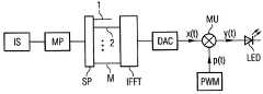
도 1a는 송신측 상에서의 가시광 통신 시스템의 구조를 도시하는 블록도(block diagram)를 도시하고;
도 1b는 수신기측 상에서의 가시광 통신 시스템의 구조를 도시하는 블록도를 도시하고;
도 2는 펄스-폭 변조된 신호를 도시하는 시간 다이어그램(timing diagram)을 도시하고;
도 3은 복합 신호를 도시하는 시간 다이어그램을 도시하고;
도 4는 펄스-폭 변조된 신호를 도시하는 시간 다이어그램을 도시하고;
도 5a는 멀티캐리어 신호 및 펄스-폭 변조된 신호가 비동기화되는 일반적 경우의 비율(RS)에 대해 SIR 값들의 역(inverse)을 도시하고;
도 5b는 멀티캐리어 신호 및 펄스-폭 변조된 신호가 동기화되는, 비율(RS)에 대해 SIR 값들의 역을 도시하고;
도 6a는 송신측 상에서의 가시광 통신 시스템의 대안적 실시예의 구조를 도시하는 블록도를 도시하고;
도 6b는 수신기측 상에서의 가시광 통신 시스템의 대안적 실시예의 구조를 도시하는 블록도를 도시한다.FIG. 1A shows a block diagram illustrating the structure of a visible light communication system on a transmitting side; FIG.
1B shows a block diagram showing the structure of a visible light communication system on the receiver side;
Figure 2 shows a timing diagram illustrating the pulse-width modulated signal;
Figure 3 shows a time diagram showing a composite signal;
Figure 4 shows a time diagram illustrating a pulse-width modulated signal;
5A shows the inverse of the SIR values for the ratio RS of the general case where the multi-carrier signal and the pulse-width modulated signal are asynchronous;
5B shows the inverse of the SIR values for the ratio RS , where the multi-carrier signal and the pulse-width modulated signal are synchronized;
6A shows a block diagram illustrating the structure of an alternative embodiment of a visible light communication system on the transmit side;
6B shows a block diagram illustrating the structure of an alternative embodiment of a visible light communication system on the receiver side.
도 1a에서, 송신측 상에서의 가시광 통신 시스템의 구조를 도시하는 블록도가 도시된다.In Fig. 1A, a block diagram showing the structure of a visible light communication system on the transmission side is shown.
임의의 종류의 정보 소스(IS)는 데이터 비트 시퀀스의 형태로 정보를 공급한다. 데이터 비트 시퀀스에 포함된 데이터는, 광학 송신기(LED)를 포함하는 도 1a에 따른 광학 무선 데이터 송신 시스템을 위한 코딩 시스템에 의해 변환된다.An information source (IS) of any kind supplies information in the form of a data bit sequence. The data contained in the data bit sequence is transformed by a coding system for the optical wireless data transmission system according to FIG. 1A including an optical transmitter (LED).
데이터는 변환 유닛(MP)에 피딩되고, 여기서 데이터 비트들은 예를 들어, QAM(직교 진폭 변조) 성상도 매퍼(constellation mapper)를 이용하여, 심볼들의 시퀀스로 변환된다.The data is fed to a conversion unit MP where the data bits are converted into a sequence of symbols, for example, using a QAM (quadrature amplitude modulation) constellation mapper.
변환 유닛(MP)에 의해 생성된 심볼들은 직렬-대-병렬 변환기(SP)에 피딩된다. 이 변환기(SP)는 심볼들을 다수(M)의 병렬 시퀀스들(1,2,3,...,M)로 분할한다.The symbols generated by the conversion unit MP are fed to the serial-to-parallel converter SP. The converter SP divides the symbols into a plurality (M) of parallel sequences (1,2,3, ..., M).
상기 다수의 병렬 시퀀스들은 각각의 서브캐리어 주파수를 갖는 다수의 직교 서브캐리어들(M)에 대응한다. 시퀀스 번호 1은 0 Hertz의 서브캐리어 주파수, 즉 DC를 갖는 서브캐리어(1)에 대응하고, 시퀀스 번호 M은 최대 서브캐리어 주파수를 갖는 서브캐리어(M)에 대응하거나, 또는 다시 말해, 이 서브캐리어는 가장 빠른 발진 서브캐리어이다.The plurality of parallel sequences correspond to a plurality of orthogonal subcarriers (M) having respective subcarrier frequencies.
병렬 시퀀스들(2,3,...,M)은 변조기(IFFT)에 피딩된다. >>1<<로 표시되어 도면에서 도시된, 병렬 시퀀스들(1,2,...,M) 중 제 1 시퀀스는 변조기(IFFT)에 피딩되지 않는데, 그 이유는 0 Hertz의 서브캐리어 주파수, 또는 DC 형상을 갖는 서브캐리어에 대응하는 제 1 병렬 시퀀스는 어떠한 정보도 반송하지 않기 때문이다. 제 1 시퀀스(1)의 이러한 생략된 피딩은 변조기(IFFT)의 측에 대해 단절된, 1로 표시된 라인에 의해 도면에서 예시된다.The parallel sequences (2,3, ..., M) are fed to a modulator (IFFT). The first one of the
추가로, 실수치의 신호를 발생시키기 위해, 복소-켤레들(complex-conjugates)은 변조기(IFFT)의 탭들(M+1 ... 2M)을 이용하여 변조기(IFFT)에 피딩되지만, 순환 대칭(cyclic symmetry)은 지켜진다(adhere). 이러한 세부사항들은 도면에 도시되지 않는다.In addition, complex-conjugates are fed to the modulator (IFFT) using taps M + 1 ... 2M of the modulator (IFFT) to generate real-valued signals, but cyclic symmetries cyclic symmetry is adhere. These details are not shown in the figures.
제 1 시퀀스(1)의 단절의 설명 및 변조기(IFFT)의 탭들의 피딩의 세부사항들은, 변조기(IFFT)를 접속시키는 세부사항들의 예에 따라 이해되지만, 본 발명에 필수적인 사항들이 아니다.The description of the disconnection of the first sequence (1) and the details of the feeding of the taps of the modulator (IFFT) are understood in accordance with the example of the details of connecting the modulator (IFFT), but are not essential to the invention.
병렬 시퀀스들(2,3,...,M)은 변조기(IFFT)에 피딩되고, 상기 변조기(IFFT)에 의해, 디지털 멀티캐리어-신호를 생성하기 위해 각각의 병렬 시퀀스(2,3,...,M)는 상기 각각의 병렬 시퀀스의 할당된 서브캐리어에 의해 변조되고, 상기 디지털 멀티캐리어-신호는 디지털-아날로그 변환기(DAC)에 의해 아날로그 멀티캐리어-신호(x(t))로 변환된다.The
멀티캐리어-신호로의 변조를 위해, 각각의 서브캐리어 시퀀스의 할당된 서브캐리어 주파수를 이용하여 각각의 서브캐리어 시퀀스의 역 푸리에 변환 연산이, 변조기(IFFT)에 의해 수행된다. 대안적인 변조 연산들이 또한 본 발명의 범위 내에 있다.For modulation into a multicarrier-signal, an inverse Fourier transform operation of each subcarrier sequence is performed by a modulator (IFFT) using the assigned subcarrier frequency of each subcarrier sequence. Alternative modulation operations are also within the scope of the present invention.
발생된 멀티캐리어 신호(x(t))는 곱셈기(multiplier; MU) 내에서 주기적 펄스-폭-변조된 펄스 트레인(p(t))과 곱해진다. 결과적인 복합 신호(
이 펄스-폭-변조된 신호(p(t))는 디밍 유닛(PWM)에 의해 전달되고, 상기 디밍 유닛(PWM)은 송신기(LED)의 방사 강도를 조절하기 위한 디밍 인자에 따라 펄스 폭을 조절하기 위해 이용된다.The pulse-width-modulated signal p (t) is delivered by a dimming unit PWM, and the dimming unit PWM adjusts the pulse width according to the dimming factor for adjusting the radiant intensity of the transmitter (LED) .
펄스-폭 변조, 또는 PWM은 광범위한 디밍 범위에 걸쳐 광학 송신기(LED)에 의해 방출되는 평균 광학 파워를 조절하기 위한 매우 효율적인 수단이다. PWM 신호는 펄스들의 주기적 트레인으로 구성되고, 이에 의해 사이클 내의 펄스 폭은 조절되고, 결과적으로 파형의 DC 레벨(level)의 변화가 초래된다.Pulse-width modulation, or PWM, is a very efficient means for adjusting the average optical power emitted by an optical transmitter (LED) over a wide dimming range. The PWM signal is made up of a periodic train of pulses, whereby the pulse width in the cycle is adjusted, resulting in a change in the DC level of the waveform.
디밍 인자를 조절하는 것은 송신될 데이터의 코딩에 독립적인데, 그 이유는 데이터를 송신하기 위한 코딩된 신호(x(t))는 펄스-폭-변조된 신호(p(t))와의 곱셈 연산에 의해 단순하게 영향받기(impinge) 때문이라는 것이 유의된다.Adjusting the dimming factor is independent of the coding of the data to be transmitted because the coded signal x (t) for transmitting the data is multiplied by the pulse-width-modulated signal p (t) It is to be noted that this is simply because of the impinge.
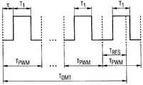
펄스-폭 변조된 신호(p(t))는 d=T1/TPWM의 듀티 사이클에 의해 특징화되고, 여기서 T1은 PWM 펄스의 지속기간이고, TPWM은 펄스-폭 변조된 신호의 주기이다. 디밍 레벨(

이제, 가시광 통신 시스템의 수신기측 또는 디코딩 시스템을 도시하는 도 1b로 돌아가면, 송신된 복합 신호(y(t))는 광학 수신기(PD), 예컨대 포토다이오드(photodiode)에 의해 수신된다. 수신된 광학 복합 신호(y(t))는 광학 수신기(PD)에 의해 전기 신호로 변환되고, 전기 신호는 아날로그-디지털 변환기(ADC)에 피딩된다.Turning now to Fig. 1B, which shows the receiver side or decoding system of the visible light communication system, the transmitted composite signal y (t) is received by an optical receiver (PD), e.g. a photodiode. The received optical composite signal y (t) is converted into an electrical signal by the optical receiver PD, and the electrical signal is fed to an analog-to-digital converter (ADC).
아날로그-디지털 변환기(ADC)의 출구(outlet)는 1개-탭(one-tap)으로 등화되고(one-tap equalized), 각각의 서브캐리어 주파수를 갖는 개별적으로 할당된 서브캐리어를 이용하여 신호를 개별적으로 복조함으로써 디지털 신호를 다수의 병렬 시퀀스들(2,3,...,M)로 복조하기 위한 복조기(FFT)에 피딩된다. 이 실시예에서, 1개-탭 등화 연산은 복조기(FFT)에서 실행된다. 대안적인 실시예에서(도 6b참조), 이러한 1개-탭 등화 연산은 특정 디바이스(EQ)에서 실행된다.The output of an analog-to-digital converter (ADC) is one-tap equalized, and the signals are separated using an individually assigned subcarrier with each subcarrier frequency Is fed to a demodulator (FFT) for demodulating the digital signal into a plurality of parallel sequences (2,3, ..., M) by demodulating individually. In this embodiment, the one-tap equalization operation is performed in a demodulator (FFT). In an alternative embodiment (see FIG. 6B), this one-tap equalization operation is performed in a specific device (EQ).
멀티캐리어-신호의 다수의 병렬 시퀀스들(2,3,...,M), 또는 기저대역 신호들로의 복조를 위해, 푸리에 변환 연산이 수행된다. 대안적인 복조 연산들은 또한, 본 발명의 범위 내에 있다.For a plurality of parallel sequences (2,3, ..., M) of a multi-carrier signal, or for demodulation into baseband signals, a Fourier transform operation is performed. Alternative demodulation operations are also within the scope of the present invention.
병렬 시퀀스들(2,3,...,M)은 병렬-대-직렬 변환기(PS)에 피딩되고 심볼들의 시퀀스로 합체된다.The parallel sequences (2,3, ..., M) are fed to a parallel-to-serial converter (PS) and merged into a sequence of symbols.
발생된 심볼들은, 각각의 서브캐리어 주파수의 자체-간섭 인자를 고려한 추정 인자들을 적용함으로써 아래에 설명되는 바와 같은 적합한 검출 방식들을 이용하는 수단― 도 1b에 도시되지 않음 ―에 의해 디코딩된다.The generated symbols are decoded by means of using suitable detection schemes as described below by applying estimation factors taking into account the self-interference factor of each sub-carrier frequency - not shown in FIG. 1B.
그 다음에 심볼들은 역-변환 유닛(DMP)에 피딩되고, 여기서 심볼들의 시퀀스는 예를 들어, QAM 성상도 매퍼를 이용하여 데이터 비트들로 역-변환된다.The symbols are then fed to a de-transformation unit (DMP), where the sequence of symbols is de-transformed into data bits using, for example, a QAM constellation mapper.
복조기(FFT) 및 병렬-대-직렬 변환기(PS)로 구성되는 신호-처리 체인(chain)은 복조기로 지칭된다.A signal-processing chain consisting of a demodulator (FFT) and a parallel-to-serial converter (PS) is referred to as a demodulator.
도 1a 및 도 1b에 따른 가시광 통신 시스템에서, >>IM/DD<<(강도 변조, 직접 검출)로 알려진 직접 검출을 이용한 강도 변조가 이용된다.In the visible light communication system according to Figs. 1A and 1B, intensity modulation using direct detection known as " IM / DD " (intensity modulation, direct detection) is used.
이제 도 6a 및 도 6b로 돌아가면, 도 6a 및 도 6b는 송신측 및 수신기측 상에서의 가시광 통신 시스템의 대안적 실시예를 각각 도시한다. 이들 대안적인 실시예들의 대부분의 디바이스들은 도 1a 및 도 1b에서 각각 설명된 실시예들과 동일하므로, 차이점들만이 논의된다.Turning now to Figures 6a and 6b, Figures 6a and 6b respectively show an alternative embodiment of a visible light communication system on the transmitter side and the receiver side. Most of the devices in these alternative embodiments are identical to the embodiments described in Figures 1A and 1B, respectively, so only the differences are discussed.
도 6a에 도시된 대안적인 실시예에 따른 송신기측은, 예로서, 디지털-아날로그 변환기(DAC)와 변조기(IFFT)의 출구들 사이에 배열된 클리핑 디바이스(clipping device; CLP)를 포함한다. 이러한 클리핑 디바이스(CLP)는, 상위 임계치(xclipp)를 초과하는 또는 하위 임계치(-xclipp) 미만으로 진행하는 임의의 신호를 상위 임계치(xclipp) 또는 -xclipp로 각각 설정한다. 이 클리핑 디바이스(CLP)의 이점은, 클리핑되지 않은 DMT 신호들은 공통적으로, 처리되지 않고 남겨지는 경우 광학 송신기(LED)에 피딩되는 평균 신호 파워(power)를 더 낮추는 과도한 포지티브(positive) 및 네거티브(negative) 피크(peak)들로부터 어려움을 당한다는 점이다.The transmitter side according to the alternative embodiment shown in FIG. 6A includes, by way of example, a clipping device (CLP) arranged between the outlets of a digital-to-analog converter (DAC) and a modulator (IFFT). The clipping device (CLP) are, respectively, set up a random signal that goes to or less than the lower threshold value (-xclipp) exceeding the upper threshold value (xclipp) to the upper threshold value (xclipp) or -xclipp. An advantage of this clipping device (CLP) is that the uncleaved DMT signals commonly have excessive positive and negative (" negative ") signals that further lower the average signal power fed to the optical transmitter (LED) negative peaks. < / RTI >
클리핑 디바이스(CLP)는 스크램블러(scrambler)와 결합될 수 있다. 스크램블러는 송신될 데이터 내의 반복적인 데이터 패턴(pattern)들, 예컨대 "1"들의 블록들의 발생을 억제한다. 동일한 데이터의 긴 반복들은 역 푸리에 변환 연산 이후에 매우 큰 신호 진폭들을 초래할 수 있고, 따라서 순환적인 강한 클리핑을 이끌고, 이는 큰 간섭 잡음 플로어(noise floor)를 초래할 것이다. 이러한 ―도시되지 않은― 스크램블러는 도 6a에서 정보 소스(IS)와 변환 유닛(MP) 사이에 삽입될 것이다. 더욱이, ―도시되지 않은― 역-스크램블러는 도 6b에서 역-변환 유닛(DMP) 이후에 필요로 될 것이다.The clipping device (CLP) may be combined with a scrambler. The scrambler suppresses the generation of repetitive data patterns, e.g., blocks of "1" s, in the data to be transmitted. Long iterations of the same data may result in very large signal amplitudes after the inverse Fourier transform operation, thus leading to cyclic strong clipping, which will result in a large interference noise floor. This non-illustrated-scrambler will be inserted between the information source IS and the conversion unit MP in Fig. 6A. Furthermore, a non-illustrated-inverse-scrambler will be needed after the inverse-transform unit DMP in FIG. 6B.
대안적으로 또는 부가적으로, 도 6a에 도시된 대안적인 실시예에 따른 수신기측은, 예로서, 곱셈기(MU)와 디지털-아날로그 변환기(DAC)의 출구들 사이에 배열된 바이어스 디바이스(bias device; T)를 포함한다. 바이어스 디바이스는, 바람직하게 신호(x(t))와 독립적으로 바람직하게 선택될 수 있는 바이어스 전류(DC)를 부가한다.Alternatively or additionally, the receiver side according to the alternative embodiment shown in FIG. 6A may include, for example, a bias device (not shown) arranged between the outputs of the multiplier MU and the digital-to-analog converter (DAC). T). The bias device preferably adds a bias current (DC) which can be preferably selected independently of the signal x (t).
다음의 섹션에서, 본 발명에 따른 검출 방식들이 상세하게 설명된다.In the following sections, detection schemes according to the present invention are described in detail.
펄스-폭-변조된 신호(p(t))는 펄스들의 주기적 트레인으로 구성되고, 이에 의해 신호의 폭들이 조절되고, 결과적으로 파형의 DC 레벨의 변화를 초래한다. 펄스-폭-변조된 신호(p(t))는 다음 식에 의해 주어지고,The pulse-width-modulated signal p (t) consists of a periodic train of pulses, whereby the widths of the signals are adjusted, resulting in a change in the DC level of the waveform. The pulse-width-modulated signal p (t) is given by the following equation,

여기서, TPWM은 펄스-폭-변조된 신호(p(t))의 주기이고, T1은 >>온<<-타임 간격이다.Where TPWM is the period of the pulse-width-modulated signal p (t) and T1 is the " on " -time interval.
도 2는 광학 송신기(LED)의 >>온<<-타임(T1) 및 펄스-폭 변조된 신호의 주기(TPWM)를 지시하는, 20%의 디밍 인자를 갖는 펄스-폭-변조된 신호(p(t))의 시간 다이어그램을 도시한다. PWM 신호(p(t))는 가로좌표 상의 밀리초 단위의 시간에 대해 세로좌표 상에 플로팅된다.Figure 2 >> on << of the optical transmitter (LED) - time (T1) and a pulse-modulated-width of the modulated signal period (TPWM) an instruction to a pulse having a dimming factor of 20% to the width Shows a time diagram of the signal p (t). The PWM signal p (t) is plotted on the ordinate for time in milliseconds on the abscissa.
도 3은 동일한 설정들에 대한 각각의 복합 신호(y(t))의 시간 다이어그램을 도시한다. 복합 신호(y(t))의 정상화된 방사된 파워는 가로좌표 상의 밀리초 단위의 시간에 대해 세로좌표 상에 플로팅된다(plotted).Figure 3 shows a time diagram of each composite signal y (t) for the same settings. The normalized radiated power of the composite signal y (t) is plotted on the ordinate for time in milliseconds on the abscissa.
펄스-폭-변조된 신호(p(t))의 반복 레이트(fPWM = 1/TPWM)는 주의 깊게 선택되어야 한다. fPWM에 대한 높은 값은 구동 전류 스펙트럼의 상당 부분이 LED의 3-dB 변조 대역폭 외측에 놓이는 것을 초래하고, 이는 비효율적인 전류-대-광 변환 효율성을 초래한다. 반면, fPWM의 매우 낮은 값들은 광학 송신기(LED)의 플리커링(flickering)을 초래할 수 있다.The repetition rate (fPWM = 1 / TPWM ) of the pulse-width-modulated signal p (t) should be carefully selected. A high value for fPWM results in a significant portion of the drive current spectrum being placed outside the 3-dB modulation bandwidth of the LED, leading to inefficient current-to-photo conversion efficiency. On the other hand, very low values of fPWM can lead to flickering of the optical transmitter (LED).
본 발명에 따라, >>이산 멀티톤 변조<<, DMT와 같은 다수의 서브캐리어 방식들이, 광학 송신기(LED)의 주파수 의존성을 보상하기 위해 이용된다.In accordance with the present invention, multiple subcarrier schemes such as " Discrete Multitone Modulation ", DMT, are used to compensate for the frequency dependence of the optical transmitter (LED).
클리핑되지 않은 DMT-신호(x(t))는 주파수 축에서

여기서,


그러므로,


식(2)는
DMT 및 PWM 신호들이 복합 신호(y(t))로 결합되는 경우에, 광학 송신기(LED)를 구동시키는 전류(y(t))는 DMT 및 PWM 파형들의 곱이며, 즉 다음 식과 같다:The current y (t) driving the optical transmitter (LED), when the DMT and PWM signals are combined into the composite signal y (t), is the product of the DMT and PWM waveforms,

다음에서, PWM과 DMT의 결합은 >>PWM-DMT 변조<<로 지칭된다.In the following, the combination of PWM and DMT is referred to as " PWM-DMT modulation ".
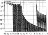
PWM 주기에 걸친 DMT 심볼 지속기간의 비율(R),


본 발명자들은 R>1의 정수 및 비정수 값들 둘 다에 대한 PWM-DMT 성능을 연구하였다. 도 3은 모든 서브캐리어들에 대해 16-QAM(N=16) 및 31 개의 서브캐리어들(M=32)을 갖는 PWM-샘플링된(sampled) DMT 신호의 예를 도시한다. 가장 빠른 발진 서브캐리어는


다음에서, 심볼 디코딩이 설명된다.In the following, symbol decoding is described.
3-dB 대역폭을 갖는 선형 광학 송신기(LED)가 신호 대역폭보다 상당히 큰 것으로 가정하면, 방출된 광학 파워는 구동 전류(y(t))에 비례한다. 관심 있는 변조-주파수 범위에서, 자유-공간 채널은 평탄하며, 서브캐리어(m)에 대한 수신된 디코딩된 심볼(

비례 상수(proportionality constant)(A)는 LED 전류-대-광 변환 효율성, 광학 채널의 이득, 및 광-대-전류 변환 효율성뿐만 아니라 수신기에서의 증폭기 이득도 포함한다. 이 이득은, 수신된 심볼들의 성상도에서의 간격이 송신된 심볼들의 성상도에서의 간격과 동일하도록 선택된다.The proportionality constant A includes not only the LED current-to-photo conversion efficiency, the gain of the optical channel, and the photo-to-current conversion efficiency, but also the amplifier gain at the receiver. This gain is chosen such that the interval in the constellation of received symbols is equal to the interval in the constellation of transmitted symbols.
전기-광학 컴포넌트들의 비-평탄 채널 및/또는 비-평탄 주파수 응답은, 적절한 주파수 응답을 이용하여 식(4)의 우측을 나눔으로써 용이하게 통합될 수 있다.The non-planar channel and / or non-planar frequency response of the electro-optical components can be easily integrated by dividing the right side of equation (4) using the appropriate frequency response.
수신기에서의 심볼 추정들에 대한 식을 유도하기 위해, 일반적인 경우가 설명되기 전에, 간략화를 위해,


여기서

식(5)에서, 항


DMT 신호(x(t))의 지수 항들은 내적(inner product) 하에서 직교하며,The exponential terms of the DMT signal (x (t)) are orthogonal under the inner product,

그리고 따라서, PWM의 부재시, 즉 y(t)=x(t)에서, 이들 신호들은 식(4)에서 간섭하지 않는다. 그러나, PWM의 존재시, 서브캐리어 신호 컴포넌트들은 식(4)에서 그들의 복소-켤레들과 간섭할 것이며, 이는 자체-간섭 컴포넌트
식(7)에 따라, 설정 AP(0)=1은, PWM-유도된 간섭의 존재시에, 수신된 그리고 송신된 QAM 심볼들이 성상도에서 동일한 간격을 가질 것이라는 것을 보장한다. 2개의 서브캐리어들에 대해 제시된 것과 동일한 접근방식을 이용하여, M-1개의 서브캐리어들을 갖는 PWM-DMT 신호에 대한 추정을 유도할 수 있다:According to equation (7), the set AP (0) = 1 ensures that, in the presence of PWM-induced interference, the received and transmitted QAM symbols will have the same spacing in constellation. Using the same approach as presented for two subcarriers, one can derive an estimate for a PWM-DMT signal with M-1 subcarriers:

식(8)의 합산 항은 다음과 같이,The summation term in Eq. (8)

m번째 서브캐리어에 대한 모든 다른 서브캐리어 채널들의 상호-간섭을 고려한다. 본 발명에 따라, 펄스-폭 변조된 신호에 대한 반복 주파수가 가장 빠른 발진 서브캐리어에 할당된 주파수의 적어도 2배로 설정되는 경우, 이 항은 실질적으로 0이 된다.Consider the inter-interference of all other sub-carrier channels for the m-th sub-carrier. According to the invention, this term is substantially zero if the repetition frequency for the pulse-width modulated signal is set to at least twice the frequency assigned to the fastest oscillation subcarrier.
본 발명의 추가의 실시예에 따라, 펄스-폭 변조된 신호(p(t)) 및 멀티캐리어-신호(x(t))가 동일위상에 동시에 유지되는 경우, 이 항은 심지어 0으로 보다 빨리 수렴된다.In accordance with a further embodiment of the present invention, when the pulse-width modulated signal p (t) and the multicarrier-signal x (t) are simultaneously held in phase, Convergence.
그러므로, 심볼들을 디코딩하기 위한 본 발명의 수단은,Therefore, the means of the present invention for decoding symbols,
- 펄스-폭 변조된 신호 및 아날로그 멀티캐리어-신호가 동일위상에 동시에 유지되고; 그리고The pulse-width modulated signal and the analog multicarrier signal are simultaneously held in phase; And
- 복합 신호 내의 펄스-폭 변조된 신호의 반복 주파수가, 가장 빠른 발진 서브캐리어의 할당된 주파수의 적어도 2배로 조절되는 경우에, 이는 제 1 서브캐리어 주파수와 상이한 모든 다른 서브캐리어 주파수들에 대한 각각의 제 1 서브캐리어 주파수의 간섭을 구성하는 상호-간섭 인자를 억제한다.If the repetition frequency of the pulse-width modulated signal in the composite signal is adjusted to be at least twice the assigned frequency of the fastest oscillation subcarrier, then this means that for each of the different subcarrier frequencies different from the first subcarrier frequency Lt; RTI ID = 0.0 > interfere < / RTI >
간섭 인자를 억제하는 것은 특히, 상기 식들에 따라 이 인자를 추정하고 추정된 인자를 감산하기 위한 수단일 수 있다.Suppressing interference factors may be in particular means for estimating this factor and subtracting the estimated factor according to the above equations.
이후 각각의 서브캐리어 주파수의 자체-간섭 인자로 지칭되는, 식(8)의 다른 부분적 항,Another subset of Equation (8), hereinafter referred to as the self-interference factor of each subcarrier frequency,


또한, 이후 >>DC 컴포넌트<<로 지칭되는, 식(8)의 부분적 항,Also, a partial term of equation (8), hereinafter referred to as " DC component &


다음에서, 본 발명의 다른 양상에 따른 펄스-폭 변조된 신호(p(t))의 동기화 및 멀티캐리어-신호(x(t)) 동기화가 설명된다.Next, synchronization of the pulse-width modulated signal p (t) and multicarrier-signal (x (t)) synchronization in accordance with another aspect of the present invention is described.


R은 일반적으로 정수가 아니기 때문에, 잔여 지속기간
도 4는 멀티캐리어-신호(x(t))의 사이클(T)(도 4에서 TDMT로 표시됨)과 펄스-폭 변조된 신호(p(t))의 사이클(TPWM) 사이의 비-정수 관계(R)의 경우에서의 펄스-폭 변조된 신호(p(t))를 도시한다.Fig. 4 shows a non-cross-section between the cycle T of the multicarrier-signal x (t) (denoted TDMT in Fig. 4) and the cycle TPWM of the pulse-width modulated signal p (t) Shows the pulse-width modulated signal p (t) in the case of the integer relation (R).
그러므로,


여기서,here,

및And

이다.to be.
스펙트럼(

식(9) 내지 식(11)에 따라, 스펙트럼(


식(8)의 어떠한 대수학적 처리(algebraic manipulation) 이후에, 심볼 추정치들의 실수부 및 허수부(


에르고드적(ergodic) 심볼 스트림들에 대해,


상기 결과들을 이용하여, 본 발명자들은 m번째 서브캐리어에 대해, 다음과 같이 SIR로 지칭되는 신호-대-간섭비를 규정하며:Using the above results, we define, for the m-th subcarrier, a signal-to-interference ratio, referred to as SIR, as follows:

여기서,
비율(


도 5a에서 역 SIR 값의 최소치는 도 5b에서 점선으로 그리고 실선으로 각각 표시된다. 역 SIR 값의 최대치는 도 5a에서 실선으로 그리고 도 5b에서 점선으로 각각 표시된다. 도면들 양측 모두에서, 역 SIR 값들은 비율(
도 5a는 일반적인 경우에 대응하고, 여기서 멀티캐리어 신호(x(t)) 및 펄스-폭 변조된 신호(p(t))는 비동기화되며, 즉 도 4에 도시된 바와 같은 DMT 심볼과 PWM 펄스의 포지티브 에지 사이에 랜덤 변위(
도 5b는
도 5a에 도시된 비동기화의 경우에서, 역 SIR 값들의 최대치 및 최소치는 변화하는 R에 따른 급속 변동들을 나타낸다.In the case of the asynchronism shown in Fig. 5A, the maximum value and the minimum value of the inverse SIR values represent rapid fluctuations according to the varying R values.
역 SIR이
최소 1/SIR은

도면들은

펄스-폭 변조된 신호(p(t))의 반복 주파수를, 멀티캐리어-신호의 가장 빠른 발진 서브캐리어에 할당된 주파수의 적어도 2배로의 본 발명의 조정은 니크비스트 기준(Nykvist criterion)의 단순한 애플리케이션(application)이 아니라는 점을 주목하는 것이 중요하다. 니크비스트 기준은 극히(infinitesimally) 짧은 샘플링 펄스들, 이른바 디랙(Dirac) 펄스들에 의존하지만, 본 발명에 따른 샘플링 펄스들로서 기능하는 PWM 펄스들은 상당한 길이들을 나타낸다.The tuning of the present invention with the repetition frequency of the pulse-width modulated signal p (t) at least twice the frequency assigned to the fastest oscillation subcarrier of the multicarrier-signal is a simple (nykvist criterion) It is important to note that this is not an application. The Nyquist criterion relies on infinitesimally short sampling pulses, so-called Dirac pulses, but PWM pulses functioning as sampling pulses according to the present invention exhibit considerable lengths.
유한 길이의 샘플링 펄스들은 DMT 서브캐리어들의 직교성을 손상시키고 복조시 간섭 항을 초래하며, 이는 식(8)의 우측 상에서 좌측으로부터 2개의 항이다. 그러나, 이 항에 대한 분석적 표현이 제공되고, 그리고 특정 디밍 레벨이 선택되는 경우에 전송되는 트레이닝 심볼들, 즉 미리-규정된 비트 패턴들에 의해 이 정적 간섭 항은 용이하게 추정될 수 있고, 복조된 신호로부터 수치적으로 감산될 수 있으며, 이는 에러-없는 DMT 송신을 초래하거나 그렇지 않으면 노이즈-없는 채널을 초래한다. 동일한 트레이닝(training) 심볼들은 식(8)의 DC 항을 추론하기 위해 사용될 수 있다.Finite-length sampling pulses impair the orthogonality of the DMT subcarriers and result in an interference term in demodulation, which is two terms from the left on the right-hand side of Eq. (8). However, this analytical expression for this term is provided, and this static interference term can be easily estimated by training symbols, i.e., pre-defined bit patterns, transmitted when a particular dimming level is selected, , Resulting in an error-free DMT transmission or otherwise result in a noise-free channel. The same training symbols can be used to infer the DC term in equation (8).
송신기측 상의 왜곡되지 않은(undistorted) 펄스-폭 변조된 신호에 대한 액세스를 갖는 경우에, 멀티캐리어-신호(x(t))를 동기화하는 것은, 예컨대, PWM 파형의 상승 에지에 대해 트리거링(trigger)함으로써 간단한 방식으로 달성될 수 있다. 그러므로,
Claims (13)
Translated fromKorean송신될 데이터(data)의 심볼(symbol)들을 복수의 병렬 시퀀스(parallel sequence)들로 분할(segment)하기 위한 수단 ― 상기 복수의 병렬 시퀀스들은 비례적 서브캐리어(subcarrier) 주파수를 갖는 복수의 직교 서브캐리어들에 대응함 ―;
펄스-폭(pulse-width) 변조된 신호에 대한 반복 주파수를, 가장 빠른 발진 서브캐리어(fastest oscillating subcarrier)에 할당된 서브캐리어 주파수의 적어도 2배로 조절하기 위한 수단;
각각의 병렬 시퀀스를 상기 각각의 병렬 시퀀스의 할당된 서브캐리어에 의해 변조함으로써 멀티캐리어(multicarrier) 신호를 발생시키기 위한 수단;
상기 멀티캐리어-신호를 아날로그 멀티캐리어-신호로 변환하기 위한 수단; 및
상기 아날로그 멀티캐리어-신호를 상기 펄스-폭 변조된 신호와 곱함으로써 복합 신호를 발생시키고 그리고 상기 복합 신호를 상기 광학 송신기에 피딩(feeding)하기 위한 수단
을 포함하는,
광학 무선 데이터 송신 시스템을 위한 코딩 시스템.CLAIMS 1. A coding system for an optical wireless data transmission system comprising an optical transmitter,
Means for segmenting symbols of data to be transmitted into a plurality of parallel sequences, the plurality of parallel sequences comprising a plurality of orthogonal sub-carriers having a proportional sub- Corresponding to carriers;
Means for adjusting the repetition frequency for the pulse-width modulated signal to at least twice the subcarrier frequency assigned to the fastest oscillating subcarrier;
Means for generating a multicarrier signal by modulating each parallel sequence with an assigned subcarrier of each parallel sequence;
Means for converting the multi-carrier signal into an analog multi-carrier signal; And
Means for multiplying the analog multi-carrier signal by the pulse-width modulated signal to generate a composite signal and feeding the composite signal to the optical transmitter;
/ RTI >
Coding system for optical wireless data transmission system.
상기 멀티캐리어-신호를 발생시키기 위한 수단은, 각각의 서브캐리어 시퀀스의 할당된 서브캐리어 주파수를 이용하여 상기 각각의 서브캐리어 시퀀스의 역 푸리에 변환 연산(inverse Fourier transform operation)을 적용하는,
광학 무선 데이터 송신 시스템을 위한 코딩 시스템.The method according to claim 1,
Wherein the means for generating the multicarrier signal comprises means for applying an inverse Fourier transform operation of each subcarrier sequence using an assigned subcarrier frequency of each subcarrier sequence,
Coding system for optical wireless data transmission system.
상기 멀티캐리어-신호를 발생시키기 위한 수단은 복소-켤레 서브캐리어(complex-conjugated subcarrier)들의 부가를 적용하는,
광학 무선 데이터 송신 시스템을 위한 코딩 시스템.3. The method of claim 2,
The means for generating the multicarrier signal may comprise means for applying the addition of complex-conjugated subcarriers,
Coding system for optical wireless data transmission system.
송신될 데이터의 심볼들은 직교-진폭 성상도 매퍼(constellation mapper)를 이용함으로써 데이터 비트(bit)들로부터 변환되는,
광학 무선 데이터 송신 시스템을 위한 코딩 시스템.4. The method according to any one of claims 1 to 3,
The symbols of the data to be transmitted are transformed from the data bits by using a quadrature-amplitude constellation mapper,
Coding system for optical wireless data transmission system.
상기 펄스-폭 변조된 신호의 주기의 배수는 상기 아날로그(analogue) 멀티캐리어 신호의 주기와 일치하는,
광학 무선 데이터 송신 시스템을 위한 코딩 시스템.4. The method according to any one of claims 1 to 3,
Wherein a multiple of the period of the pulse-width modulated signal coincides with a period of the analog multi-
Coding system for optical wireless data transmission system.
상기 펄스-폭 변조된 신호 및 상기 아날로그 멀티캐리어 신호는 동일위상에 동시에 유지되는,
광학 무선 데이터 송신 시스템을 위한 코딩 시스템.4. The method according to any one of claims 1 to 3,
Wherein the pulse-width modulated signal and the analog multi-carrier signal are simultaneously held in phase,
Coding system for optical wireless data transmission system.
상기 멀티캐리어-신호의 상위 및 하위 임계치들을 제한하기 위한 클리핑 디바이스(clipping device; CLP)를 포함하는,
광학 무선 데이터 송신 시스템을 위한 코딩 시스템.4. The method according to any one of claims 1 to 3,
And a clipping device (CLP) for limiting upper and lower thresholds of the multicarrier signal.
Coding system for optical wireless data transmission system.
상기 멀티캐리어-신호의 반복적 데이터 패턴(pattern)들의 발생을 억제하기 위한 스크램블러(scrambler)를 포함하는,
광학 무선 데이터 송신 시스템을 위한 코딩 시스템.4. The method according to any one of claims 1 to 3,
And a scrambler for suppressing the occurrence of repetitive data patterns of the multicarrier signal.
Coding system for optical wireless data transmission system.
광학 신호를 수신하고 상기 광학 신호를 전기 신호로 변환하기 위한 광학 수신기 ― 상기 광학 신호는 아날로그 멀티캐리어-신호와 펄스-폭 변조된 신호의 곱셈에 의한 복합 신호임―;
상기 전기 신호를 디지털(digital) 신호로 변환하기 위한 수단;
각각의 서브캐리어 주파수를 갖는 개별적으로 할당된 서브캐리어를 이용하여 상기 디지털 신호를 개별적으로 복조함으로써 상기 디지털 신호를 복수의 병렬 시퀀스들로 복조하기 위한 수단;
각각의 병렬 시퀀스를 심볼들로 합체(de-segment)하기 위한 수단; 및
DC 항(term) 및 각각의 서브캐리어 주파수의 자체-간섭 인자를 고려한 추정 인자들을 적용함으로써 상기 심볼들을 디코딩하기 위한 수단 ― 이에 의해 추정 인자들 양측 모두가 개별 서브캐리어들의 각각의 복조된 신호로부터 감산됨 ―
을 포함하고,
상기 심볼들을 디코딩하기 위한 수단은,
상기 펄스-폭 변조된 신호 및 상기 아날로그 멀티캐리어-신호가 동일위상에 동시에 유지되고; 그리고
상기 복합 신호 내의 상기 펄스-폭 변조된 신호의 반복 주파수가, 가장 빠른 발진 서브캐리어에 할당된 서브캐리어 주파수의 적어도 2배로 조절되는 경우에,
제 1 서브캐리어 주파수와 상이한 모든 다른 서브캐리어 주파수들에 대한 각각의 제 1 서브캐리어 주파수의 간섭을 구성하는 상호-간섭(cross-interference) 인자를 억제하는,
광학 무선 데이터 송신 시스템을 위한 디코딩 시스템.A decoding system for an optical wireless data transmission system,
An optical receiver for receiving an optical signal and for converting the optical signal into an electrical signal, the optical signal being a composite signal by multiplying an analog multicarrier signal with a pulse-width modulated signal;
Means for converting the electrical signal to a digital signal;
Means for demodulating the digital signal into a plurality of parallel sequences by individually demodulating the digital signal using individually assigned subcarriers having respective subcarrier frequencies;
Means for de-segmenting each parallel sequence into symbols; And
Means for decoding the symbols by applying estimation factors that take into account the DC term and the self-interference factor of each sub-carrier frequency such that both of the estimated factors are subtracted from each demodulated signal of the individual sub- -
/ RTI >
Wherein the means for decoding the symbols comprises:
Wherein the pulse-width modulated signal and the analog multicarrier signal are simultaneously held in phase; And
If the repetition frequency of the pulse-width modulated signal in the composite signal is adjusted to at least twice the subcarrier frequency assigned to the fastest oscillation subcarrier,
Suppressing cross-interference factors that constitute the interference of each first sub-carrier frequency for all other sub-carrier frequencies that are different from the first sub-
A decoding system for an optical wireless data transmission system.
송신될 데이터의 심볼들을 복수의 병렬 시퀀스들로 분할하는 단계 ― 상기 복수의 병렬 시퀀스들은 각각의 서브캐리어 주파수를 갖는 복수의 직교 서브캐리어들에 대응함 ―;
가장 빠른 발진 서브캐리어에 할당된 서브캐리어 주파수의 적어도 2배인 펄스-폭 변조된 신호를 위한 반복 주파수를 선택하는 단계;
각각의 병렬 시퀀스를 상기 각각의 병렬 시퀀스의 할당된 서브캐리어에 의해 변조함으로써 멀티캐리어-신호를 발생시키는 단계;
상기 멀티캐리어-신호를 아날로그 멀티캐리어-신호로 변환하는 단계;
상기 아날로그 멀티캐리어-신호에 상기 펄스-폭 변조된 신호를 곱함으로써 복합 신호를 발생시키는 단계; 및
상기 복합 신호를 상기 광학 송신기에 피딩하는 단계
를 포함하는,
광학 무선 데이터 송신 방법.An optical wireless data transmission method in which an optical transmitter is fed by a pulse-width modulated signal,
Dividing symbols of data to be transmitted into a plurality of parallel sequences, the plurality of parallel sequences corresponding to a plurality of orthogonal subcarriers having respective subcarrier frequencies;
Selecting a repetition frequency for a pulse-width modulated signal that is at least twice the subcarrier frequency assigned to the fastest oscillating subcarrier;
Generating a multicarrier-signal by modulating each parallel sequence by the assigned subcarriers of each parallel sequence;
Converting the multi-carrier signal into an analog multi-carrier signal;
Generating a composite signal by multiplying the analog multi-carrier signal by the pulse-width modulated signal; And
Feeding the composite signal to the optical transmitter
/ RTI >
Optical wireless data transmission method.
광학 수신기에 의해 상기 복합 신호를 수신하는 단계;
상기 복합 신호를 디지털 복합 신호로 변환하는 단계;
각각의 서브캐리어 주파수를 갖는 개별적으로 할당된 서브캐리어를 이용하여 상기 신호를 개별적으로 복조함으로써 상기 디지털 신호를 복수의 병렬 시퀀스들로 복조하는 단계;
각각의 병렬 시퀀스를 심볼들로 합체하는 단계;
DC 항 및 각각의 서브캐리어 주파수의 자체-간섭 인자를 고려한 추정 인자들을 적용함으로써 상기 심볼들을 디코딩하는 단계 ― 이에 의해 추정 인자들 양측 모두가 개별 서브캐리어들의 각각의 변조 신호로부터 감산됨 ―
를 포함하는,
광학 무선 데이터 송신 방법.12. The method of claim 11,
Receiving the composite signal by an optical receiver;
Converting the composite signal into a digital composite signal;
Demodulating the digital signal into a plurality of parallel sequences by individually demodulating the signals using individually assigned subcarriers having respective subcarrier frequencies;
Combining each parallel sequence into symbols;
Decoding the symbols by applying estimation factors that take into account the DC term and the self-interference factor of each sub-carrier frequency, whereby both of the estimated factors are subtracted from each modulated signal of the individual sub-
/ RTI >
Optical wireless data transmission method.
상기 심볼들을 디코딩하기 위해, 상기 복합 신호 내의 펄스-폭 변조된 신호의 반복 주파수가 상기 가장 빠른 발진 서브캐리어의 할당된 주파수의 적어도 2배로 조절되는 경우에, 제 1 서브캐리어 주파수와 상이한 모든 다른 서브캐리어 주파수들에 대한 각각의 제 1 서브캐리어 주파수의 간섭을 구성하는 상호-간섭 인자는 무시되는(neglect),
광학 무선 데이터 송신 방법.13. The method of claim 12,
In order to decode the symbols, if the repetition frequency of the pulse-width modulated signal in the composite signal is adjusted to at least twice the assigned frequency of the fastest oscillation subcarrier, all other different sub- The inter-interference factors that constitute the interference of each first sub-carrier frequency to the carrier frequencies are neglected,
Optical wireless data transmission method.
Applications Claiming Priority (3)
| Application Number | Priority Date | Filing Date | Title |
|---|---|---|---|
| EP09014905.5 | 2009-12-01 | ||
| EP09014905 | 2009-12-01 | ||
| PCT/EP2010/067532WO2011067103A1 (en) | 2009-12-01 | 2010-11-16 | System and arrangement for optical data transmission |
Publications (2)
| Publication Number | Publication Date |
|---|---|
| KR20120099745A KR20120099745A (en) | 2012-09-11 |
| KR101486710B1true KR101486710B1 (en) | 2015-01-28 |
Family
ID=43618177
Family Applications (1)
| Application Number | Title | Priority Date | Filing Date |
|---|---|---|---|
| KR1020127017079AExpired - Fee RelatedKR101486710B1 (en) | 2009-12-01 | 2010-11-16 | System and arrangement for optical data transmission |
Country Status (3)
| Country | Link |
|---|---|
| EP (1) | EP2484029A1 (en) |
| KR (1) | KR101486710B1 (en) |
| WO (1) | WO2011067103A1 (en) |
Cited By (1)
| Publication number | Priority date | Publication date | Assignee | Title |
|---|---|---|---|---|
| WO2020158971A1 (en)* | 2019-01-30 | 2020-08-06 | 엘지전자 주식회사 | Method of transmitting signals in visible light communication and terminal for same |
Families Citing this family (8)
| Publication number | Priority date | Publication date | Assignee | Title |
|---|---|---|---|---|
| EP3014798B1 (en)* | 2013-06-28 | 2019-03-27 | Trustees of Boston University | An optical orthogonal frequency division multiplexing (o-ofdm) system with pulse-width modulation (pwm) dimming |
| US9571312B2 (en) | 2013-11-26 | 2017-02-14 | University Of Virginia Patent Foundation | Expurgated pulse position modulation for communication |
| CN103729898B (en)* | 2013-12-20 | 2016-01-20 | 江苏大学 | Based on the ETC visible light radio communication cut-in method of LED car lamp |
| KR101509212B1 (en)* | 2014-02-03 | 2015-04-14 | 동국대학교 산학협력단 | Apparatus and methdo for transfering, apparatus and method for receiving in optical wireless communication system |
| CN103944637A (en)* | 2014-05-13 | 2014-07-23 | 江苏理工学院 | Visible light communication transmission system and method |
| CN108696470B (en)* | 2018-06-12 | 2020-09-29 | 中国地质大学(武汉) | A DMT modulation method for visible light communication |
| CN109831270B (en)* | 2019-01-28 | 2022-01-04 | 钟林晟 | Visible light secret communication system and encryption method |
| CN110830114A (en)* | 2019-11-13 | 2020-02-21 | 哈尔滨工业大学 | Pulse width modulation dimming method of variable period modulation system |
Citations (1)
| Publication number | Priority date | Publication date | Assignee | Title |
|---|---|---|---|---|
| US20060239689A1 (en)* | 2005-01-25 | 2006-10-26 | Tir Systems, Ltd. | Method and apparatus for illumination and communication |
Family Cites Families (1)
| Publication number | Priority date | Publication date | Assignee | Title |
|---|---|---|---|---|
| CN101026413B (en)* | 2006-02-17 | 2012-01-04 | 华为技术有限公司 | Lighting light wireless communication system |
- 2010
- 2010-11-16KRKR1020127017079Apatent/KR101486710B1/ennot_activeExpired - Fee Related
- 2010-11-16WOPCT/EP2010/067532patent/WO2011067103A1/enactiveApplication Filing
- 2010-11-16EPEP10781487Apatent/EP2484029A1/ennot_activeWithdrawn
Patent Citations (1)
| Publication number | Priority date | Publication date | Assignee | Title |
|---|---|---|---|---|
| US20060239689A1 (en)* | 2005-01-25 | 2006-10-26 | Tir Systems, Ltd. | Method and apparatus for illumination and communication |
Cited By (2)
| Publication number | Priority date | Publication date | Assignee | Title |
|---|---|---|---|---|
| WO2020158971A1 (en)* | 2019-01-30 | 2020-08-06 | 엘지전자 주식회사 | Method of transmitting signals in visible light communication and terminal for same |
| US11469819B2 (en) | 2019-01-30 | 2022-10-11 | Lg Electronics Inc. | Method of transmitting signals in visible light communication and terminal for same |
Also Published As
| Publication number | Publication date |
|---|---|
| EP2484029A1 (en) | 2012-08-08 |
| KR20120099745A (en) | 2012-09-11 |
| WO2011067103A1 (en) | 2011-06-09 |
Similar Documents
| Publication | Publication Date | Title |
|---|---|---|
| KR101486710B1 (en) | System and arrangement for optical data transmission | |
| Wang et al. | Optical OFDM for visible light communications | |
| Lee et al. | Modulation and coding for dimmable visible light communication | |
| Yang et al. | Novel visible light communication approach based on hybrid OOK and ACO-OFDM | |
| Grubor et al. | Bandwidth-efficient indoor optical wireless communications with white light-emitting diodes | |
| Narmanlioglu et al. | Link adaptation for MIMO OFDM visible light communication systems | |
| Ebrahimi et al. | Investigation of a hybrid OFDM-PWM/PPM visible light communications system | |
| TWI517606B (en) | Visible light communication method | |
| EP3818645B1 (en) | Optical data transmission system and method | |
| CN110166123B (en) | A hybrid visible light modulation method compatible with dimming control | |
| Mossaad et al. | Practical OFDM signalling for visible light communications using spatial summation | |
| Mirvakili et al. | Wireless access test-bed through visible light and dimming compatible OFDM | |
| Little et al. | Adaptation of OFDM under visible light communications and illumination constraints | |
| Deepthi et al. | Enhanced Optical OFDM: A novel approach for SISO and MIMO Visible Light Communication system in indoor environment | |
| WO2011082713A2 (en) | Nonlinearity compensation in optical communication systems via iterative signal clipping and a multiple led transmitter | |
| Ghassemlooy et al. | Visible light communications with hybrid OFDM-PTM | |
| Nawaf et al. | Investigation the Performance of ACO-OFDM, DCO-OFDM in Visible Light Communication System | |
| Tekin et al. | M-CSK-Flip OFDM for Visible Light Communication Systems | |
| Yaklaf et al. | Multi-carrier modulation techniques for light fidelity technology | |
| Lian et al. | Polarity-header optical OFDM for visible light communication systems | |
| Narmanlioglu et al. | Performance analysis and optimization of unipolar OFDM based relay-assisted visible light communications☆ | |
| Yang et al. | Investigation of DCT-spread OFDM transmission in indoor visible light communication | |
| Ye et al. | Experimental demonstration of NOMA visible light communications based on SCFDM | |
| KR101105738B1 (en) | Visible light transmitting device, visible light receiving device and visible light communication system including the same | |
| Afroj | Li-Fi concept in terms of modulation techniques |
Legal Events
| Date | Code | Title | Description |
|---|---|---|---|
| PA0105 | International application | St.27 status event code:A-0-1-A10-A15-nap-PA0105 | |
| R17-X000 | Change to representative recorded | St.27 status event code:A-3-3-R10-R17-oth-X000 | |
| A201 | Request for examination | ||
| P11-X000 | Amendment of application requested | St.27 status event code:A-2-2-P10-P11-nap-X000 | |
| P13-X000 | Application amended | St.27 status event code:A-2-2-P10-P13-nap-X000 | |
| PA0201 | Request for examination | St.27 status event code:A-1-2-D10-D11-exm-PA0201 | |
| PG1501 | Laying open of application | St.27 status event code:A-1-1-Q10-Q12-nap-PG1501 | |
| E902 | Notification of reason for refusal | ||
| PE0902 | Notice of grounds for rejection | St.27 status event code:A-1-2-D10-D21-exm-PE0902 | |
| T11-X000 | Administrative time limit extension requested | St.27 status event code:U-3-3-T10-T11-oth-X000 | |
| T11-X000 | Administrative time limit extension requested | St.27 status event code:U-3-3-T10-T11-oth-X000 | |
| T11-X000 | Administrative time limit extension requested | St.27 status event code:U-3-3-T10-T11-oth-X000 | |
| E13-X000 | Pre-grant limitation requested | St.27 status event code:A-2-3-E10-E13-lim-X000 | |
| P11-X000 | Amendment of application requested | St.27 status event code:A-2-2-P10-P11-nap-X000 | |
| P13-X000 | Application amended | St.27 status event code:A-2-2-P10-P13-nap-X000 | |
| E701 | Decision to grant or registration of patent right | ||
| PE0701 | Decision of registration | St.27 status event code:A-1-2-D10-D22-exm-PE0701 | |
| GRNT | Written decision to grant | ||
| PR0701 | Registration of establishment | St.27 status event code:A-2-4-F10-F11-exm-PR0701 | |
| PR1002 | Payment of registration fee | St.27 status event code:A-2-2-U10-U12-oth-PR1002 Fee payment year number:1 | |
| PG1601 | Publication of registration | St.27 status event code:A-4-4-Q10-Q13-nap-PG1601 | |
| R17-X000 | Change to representative recorded | St.27 status event code:A-5-5-R10-R17-oth-X000 | |
| R18-X000 | Changes to party contact information recorded | St.27 status event code:A-5-5-R10-R18-oth-X000 | |
| LAPS | Lapse due to unpaid annual fee | ||
| PC1903 | Unpaid annual fee | St.27 status event code:A-4-4-U10-U13-oth-PC1903 Not in force date:20180122 Payment event data comment text:Termination Category : DEFAULT_OF_REGISTRATION_FEE | |
| PC1903 | Unpaid annual fee | St.27 status event code:N-4-6-H10-H13-oth-PC1903 Ip right cessation event data comment text:Termination Category : DEFAULT_OF_REGISTRATION_FEE Not in force date:20180122 |