KR101484296B1 - Semiconductor substrate, manufacturing method of the semiconductor substrate, and semiconductor device and electronic device using the same - Google Patents
Semiconductor substrate, manufacturing method of the semiconductor substrate, and semiconductor device and electronic device using the sameDownload PDFInfo
- Publication number
- KR101484296B1 KR101484296B1KR20080052126AKR20080052126AKR101484296B1KR 101484296 B1KR101484296 B1KR 101484296B1KR 20080052126 AKR20080052126 AKR 20080052126AKR 20080052126 AKR20080052126 AKR 20080052126AKR 101484296 B1KR101484296 B1KR 101484296B1
- Authority
- KR
- South Korea
- Prior art keywords
- single crystal
- crystal semiconductor
- substrate
- insulating layer
- semiconductor substrate
- Prior art date
- Legal status (The legal status is an assumption and is not a legal conclusion. Google has not performed a legal analysis and makes no representation as to the accuracy of the status listed.)
- Expired - Fee Related
Links
Images


Classifications
- H—ELECTRICITY
- H01—ELECTRIC ELEMENTS
- H01L—SEMICONDUCTOR DEVICES NOT COVERED BY CLASS H10
- H01L21/00—Processes or apparatus adapted for the manufacture or treatment of semiconductor or solid state devices or of parts thereof
- H01L21/02—Manufacture or treatment of semiconductor devices or of parts thereof
- H01L21/04—Manufacture or treatment of semiconductor devices or of parts thereof the devices having potential barriers, e.g. a PN junction, depletion layer or carrier concentration layer
- H01L21/18—Manufacture or treatment of semiconductor devices or of parts thereof the devices having potential barriers, e.g. a PN junction, depletion layer or carrier concentration layer the devices having semiconductor bodies comprising elements of Group IV of the Periodic Table or AIIIBV compounds with or without impurities, e.g. doping materials
- H01L21/20—Deposition of semiconductor materials on a substrate, e.g. epitaxial growth solid phase epitaxy
- H—ELECTRICITY
- H10—SEMICONDUCTOR DEVICES; ELECTRIC SOLID-STATE DEVICES NOT OTHERWISE PROVIDED FOR
- H10D—INORGANIC ELECTRIC SEMICONDUCTOR DEVICES
- H10D86/00—Integrated devices formed in or on insulating or conducting substrates, e.g. formed in silicon-on-insulator [SOI] substrates or on stainless steel or glass substrates
- H10D86/01—Manufacture or treatment
- H10D86/021—Manufacture or treatment of multiple TFTs
- H10D86/0214—Manufacture or treatment of multiple TFTs using temporary substrates
- H—ELECTRICITY
- H01—ELECTRIC ELEMENTS
- H01L—SEMICONDUCTOR DEVICES NOT COVERED BY CLASS H10
- H01L21/00—Processes or apparatus adapted for the manufacture or treatment of semiconductor or solid state devices or of parts thereof
- H01L21/02—Manufacture or treatment of semiconductor devices or of parts thereof
- H01L21/04—Manufacture or treatment of semiconductor devices or of parts thereof the devices having potential barriers, e.g. a PN junction, depletion layer or carrier concentration layer
- H01L21/18—Manufacture or treatment of semiconductor devices or of parts thereof the devices having potential barriers, e.g. a PN junction, depletion layer or carrier concentration layer the devices having semiconductor bodies comprising elements of Group IV of the Periodic Table or AIIIBV compounds with or without impurities, e.g. doping materials
- H01L21/26—Bombardment with radiation
- H01L21/263—Bombardment with radiation with high-energy radiation
- H01L21/265—Bombardment with radiation with high-energy radiation producing ion implantation
- H—ELECTRICITY
- H01—ELECTRIC ELEMENTS
- H01L—SEMICONDUCTOR DEVICES NOT COVERED BY CLASS H10
- H01L21/00—Processes or apparatus adapted for the manufacture or treatment of semiconductor or solid state devices or of parts thereof
- H01L21/02—Manufacture or treatment of semiconductor devices or of parts thereof
- H01L21/04—Manufacture or treatment of semiconductor devices or of parts thereof the devices having potential barriers, e.g. a PN junction, depletion layer or carrier concentration layer
- H01L21/18—Manufacture or treatment of semiconductor devices or of parts thereof the devices having potential barriers, e.g. a PN junction, depletion layer or carrier concentration layer the devices having semiconductor bodies comprising elements of Group IV of the Periodic Table or AIIIBV compounds with or without impurities, e.g. doping materials
- H01L21/26—Bombardment with radiation
- H01L21/263—Bombardment with radiation with high-energy radiation
- H01L21/268—Bombardment with radiation with high-energy radiation using electromagnetic radiation, e.g. laser radiation
- H—ELECTRICITY
- H01—ELECTRIC ELEMENTS
- H01L—SEMICONDUCTOR DEVICES NOT COVERED BY CLASS H10
- H01L21/00—Processes or apparatus adapted for the manufacture or treatment of semiconductor or solid state devices or of parts thereof
- H01L21/02—Manufacture or treatment of semiconductor devices or of parts thereof
- H01L21/04—Manufacture or treatment of semiconductor devices or of parts thereof the devices having potential barriers, e.g. a PN junction, depletion layer or carrier concentration layer
- H01L21/18—Manufacture or treatment of semiconductor devices or of parts thereof the devices having potential barriers, e.g. a PN junction, depletion layer or carrier concentration layer the devices having semiconductor bodies comprising elements of Group IV of the Periodic Table or AIIIBV compounds with or without impurities, e.g. doping materials
- H01L21/30—Treatment of semiconductor bodies using processes or apparatus not provided for in groups H01L21/20 - H01L21/26
- H01L21/322—Treatment of semiconductor bodies using processes or apparatus not provided for in groups H01L21/20 - H01L21/26 to modify their internal properties, e.g. to produce internal imperfections
- H—ELECTRICITY
- H01—ELECTRIC ELEMENTS
- H01L—SEMICONDUCTOR DEVICES NOT COVERED BY CLASS H10
- H01L21/00—Processes or apparatus adapted for the manufacture or treatment of semiconductor or solid state devices or of parts thereof
- H01L21/70—Manufacture or treatment of devices consisting of a plurality of solid state components formed in or on a common substrate or of parts thereof; Manufacture of integrated circuit devices or of parts thereof
- H01L21/71—Manufacture of specific parts of devices defined in group H01L21/70
- H01L21/76—Making of isolation regions between components
- H01L21/762—Dielectric regions, e.g. EPIC dielectric isolation, LOCOS; Trench refilling techniques, SOI technology, use of channel stoppers
- H01L21/7624—Dielectric regions, e.g. EPIC dielectric isolation, LOCOS; Trench refilling techniques, SOI technology, use of channel stoppers using semiconductor on insulator [SOI] technology
- H01L21/76251—Dielectric regions, e.g. EPIC dielectric isolation, LOCOS; Trench refilling techniques, SOI technology, use of channel stoppers using semiconductor on insulator [SOI] technology using bonding techniques
- H01L21/76254—Dielectric regions, e.g. EPIC dielectric isolation, LOCOS; Trench refilling techniques, SOI technology, use of channel stoppers using semiconductor on insulator [SOI] technology using bonding techniques with separation/delamination along an ion implanted layer, e.g. Smart-cut, Unibond
- H—ELECTRICITY
- H10—SEMICONDUCTOR DEVICES; ELECTRIC SOLID-STATE DEVICES NOT OTHERWISE PROVIDED FOR
- H10D—INORGANIC ELECTRIC SEMICONDUCTOR DEVICES
- H10D86/00—Integrated devices formed in or on insulating or conducting substrates, e.g. formed in silicon-on-insulator [SOI] substrates or on stainless steel or glass substrates
- H10D86/40—Integrated devices formed in or on insulating or conducting substrates, e.g. formed in silicon-on-insulator [SOI] substrates or on stainless steel or glass substrates characterised by multiple TFTs
- H10D86/60—Integrated devices formed in or on insulating or conducting substrates, e.g. formed in silicon-on-insulator [SOI] substrates or on stainless steel or glass substrates characterised by multiple TFTs wherein the TFTs are in active matrices
- H—ELECTRICITY
- H01—ELECTRIC ELEMENTS
- H01L—SEMICONDUCTOR DEVICES NOT COVERED BY CLASS H10
- H01L21/00—Processes or apparatus adapted for the manufacture or treatment of semiconductor or solid state devices or of parts thereof
- H01L21/02—Manufacture or treatment of semiconductor devices or of parts thereof
- H01L21/02104—Forming layers
- H01L21/02365—Forming inorganic semiconducting materials on a substrate
- H01L21/02656—Special treatments
- H01L21/02664—Aftertreatments
- H01L21/02667—Crystallisation or recrystallisation of non-monocrystalline semiconductor materials, e.g. regrowth
- H01L21/02675—Crystallisation or recrystallisation of non-monocrystalline semiconductor materials, e.g. regrowth using laser beams
- H—ELECTRICITY
- H10—SEMICONDUCTOR DEVICES; ELECTRIC SOLID-STATE DEVICES NOT OTHERWISE PROVIDED FOR
- H10D—INORGANIC ELECTRIC SEMICONDUCTOR DEVICES
- H10D30/00—Field-effect transistors [FET]
- H10D30/01—Manufacture or treatment
- H10D30/021—Manufacture or treatment of FETs having insulated gates [IGFET]
- H10D30/031—Manufacture or treatment of FETs having insulated gates [IGFET] of thin-film transistors [TFT]
- H10D30/0321—Manufacture or treatment of FETs having insulated gates [IGFET] of thin-film transistors [TFT] comprising silicon, e.g. amorphous silicon or polysilicon
- H10D30/0323—Manufacture or treatment of FETs having insulated gates [IGFET] of thin-film transistors [TFT] comprising silicon, e.g. amorphous silicon or polysilicon comprising monocrystalline silicon
Landscapes
- Physics & Mathematics (AREA)
- Engineering & Computer Science (AREA)
- High Energy & Nuclear Physics (AREA)
- Condensed Matter Physics & Semiconductors (AREA)
- General Physics & Mathematics (AREA)
- Manufacturing & Machinery (AREA)
- Computer Hardware Design (AREA)
- Microelectronics & Electronic Packaging (AREA)
- Power Engineering (AREA)
- Health & Medical Sciences (AREA)
- Toxicology (AREA)
- Optics & Photonics (AREA)
- Electromagnetism (AREA)
- Thin Film Transistor (AREA)
- Recrystallisation Techniques (AREA)
Abstract
Translated fromKoreanDescription
Translated fromKorean본 발명은, 반도체 기판, 반도체 기판의 제작방법, 및 그 반도체 기판을 사용한 반도체 장치와 전자 기기에 관한 것이다.The present invention relates to a semiconductor substrate, a method of manufacturing a semiconductor substrate, and a semiconductor device and an electronic apparatus using the semiconductor substrate.
근년, 단결정 실리콘의 잉곳(ingot)을 얇게 슬라이스(slice)하여 제작되는 단결정 실리콘 기판 대신에, SOI(Silicon On Insulator) 기판을 사용한 집적회로의 개발이 진행되고 있다. SOI 기판은 절연성 표면에 얇은 단결정 실리콘 층을 형성한 구조를 가지고, 단결정 실리콘 기판을 사용하는 경우와 비교하여 트랜지스터의 드레인과 기판 사이에 있어서의 기생 용량을 저감함으로써 반도체 집적회로의 성능을 향상시킬 수 있다.In recent years, an integrated circuit using an SOI (Silicon On Insulator) substrate has been developed instead of a monocrystalline silicon substrate produced by slicing an ingot of monocrystalline silicon thinly. The SOI substrate has a structure in which a thin monocrystalline silicon layer is formed on the insulating surface and the parasitic capacitance between the drain of the transistor and the substrate is reduced as compared with the case of using a single crystal silicon substrate, have.
SOI 기판의 제조방법은 다양하지만, 형성되는 단결정 반도체층의 품질과 생산성(스루풋(throughput))을 양립시키는 것으로서, 스마트 컷(Smart Cut)(등록상표)법이라고 불리는 방식이 알려져 있다. 스마트 컷법에서는, 단결정 실리콘 기 판(본드 웨이퍼(bond wafer))에 수소 이온을 주입한 후, 다른 기판(베이스 웨이퍼(base wafer))과 실온에서 접합한다. 그 접합은, 반 데르 발스 힘(van der Waal's force)을 이용한 강고한 접합을 형성함으로써 행해진다. 그 후, 500℃ 정도의 온도로 열 처리함으로써, 수소 이온이 주입된 영역에서 단결정 실리콘 기판이 분리하고, 다른 기판(베이스 웨이퍼) 위에는 단결정 실리콘 층이 잔존한다.The manufacturing method of the SOI substrate is various, but a method called the Smart Cut (registered trademark) method is known in which both the quality and the productivity (throughput) of the single crystal semiconductor layer to be formed are compatible. In the smart cut method, hydrogen ions are implanted into a single crystal silicon substrate (bond wafer), and then bonded to another substrate (base wafer) at room temperature. The bonding is performed by forming a strong bond using a van der Waal's force. Thereafter, the single crystal silicon substrate is separated in the region where the hydrogen ions are implanted, and the single crystal silicon layer remains on the other substrate (base wafer).
이와 같은 스마트 컷법을 사용하여, 단결정 실리콘 박막을 유리 기판 위에 형성하는 기술의 일례로서, 본 출원인에 의한 기술이 알려져 있다(예를 들어, 문헌 1 참조).As an example of a technique for forming a monocrystalline silicon thin film on a glass substrate using such a smart cutting method, a technique by the present applicant is known (see, for example, Document 1).
문헌 1에서는, 유리 기판에 절연성 피막을 형성함으로써, 단결정 실리콘 층의 오염을 방지하여, 고성능의 반도체 장치를 제공하는 것에 성공하였다.
[문헌 1] 일본국 공개특하공고 평11-163363호 공보[Document 1] Japanese Unexamined Patent Application Publication No. 11-163363
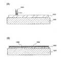
그런데, 이렇게 하여 형성된 단결정 반도체층에 대하여 레이저광을 조사하는 경우가 있다. 예를 들어, 도 16(A)에 나타내는 바와 같이, 유리 기판(1600) 위에 단결정 실리콘 박막(1602)을 형성한 후, 그 단결정 실리콘 박막(1602)에 레이저광(1604)을 조사함으로써, 표면의 평탄성을 크게 향상시킬 수 있다. 또한, 평탄성의 향상과 함께, 이온의 도입에 따른 단결정 실리콘 박막의 손상을 회복시킬 수도 있다. 도 16(A) 및 도 16(B)에 있어서는, 간략화를 위해, 유리 기판(1600) 및 단결정 실리콘 박막(1602) 이외의 적층 구조에 대해서는 생략하고 있다.The single crystal semiconductor layer thus formed may be irradiated with laser light. 16A, after the single crystal silicon
상기한 바와 같이, 단결정 실리콘 박막에 레이저광을 조사하는데 있어서는, 어느 정도의 유의해야 할 점이 있다. 그 중의 하나는, 레이저광의 강도에 대한 것이다. 단결정 실리콘 박막에 레이저광을 조사한 경우에는, 그 레이저광이 조사된 영역은 용융(융해)한다. 그리고, 레이저광의 조사가 종료하면, 그 용융한 영역은 용융하지 않은 영역을 핵(核)으로 하여 다시 결정화하는 것으로 고려된다. 여기서, 레이저광의 강도가 과대한 경우에는, 단결정 실리콘 박막이 모두 용융된다. 이 경우, 핵이 되는 단결정 실리콘이 존재하지 않으므로, 재결정에 의하여 단결정 실리콘을 얻을 수 없다. 따라서, 레이저광의 조사에 의하여 단결정 실리콘 박막의 특성 향상 등을 도모하는 경우에는, 레이저광 조사 영역에 있어서의 단결정 실리콘 박막이 모두 용융하지 않도록 레이저광의 강도를 조절할 필요가 있다.As described above, there is a certain degree of caution in irradiating the single crystal silicon thin film with laser light. One of them is the intensity of laser light. When a single crystal silicon thin film is irradiated with a laser beam, the region irradiated with the laser beam is melted (melted). When the irradiation of the laser beam is finished, it is considered that the molten region crystallizes again with the unmelted region as nuclei (nuclei). Here, when the intensity of laser light is excessive, the single crystal silicon thin film is completely melted. In this case, there is no single crystal silicon to be a nucleus, so that single crystal silicon can not be obtained by recrystallization. Therefore, in order to improve the characteristics of the single crystal silicon thin film by irradiation with the laser light, it is necessary to adjust the intensity of the laser light so that the single crystal silicon thin film in the laser light irradiation region is not melted.
여기서, 도 16(A)에 나타내는 레이저광의 조사에 의하여 단결정 실리콘 박막 이 어떻게 변화한지를 자세히 보도록 한다. 도 16(B)에서, 유리 기판(1600) 위에는 단결정 실리콘 박막(1602)이 형성되어 있다. 여기서, 단결정 실리콘 박막(1602)의 하부(1606)는 레이저광의 조사에 의하여 용융하지 않은 영역이고, 상부(1608)는 레이저광의 조사에 의하여 용융하고 재결정화한 영역이다. 하부(1606)와 상부(1608)를 비교한 경우, 상부(1608)에서는 결정성이 회복되어 있고, 또한, 이온의 도입에 따른 미량의 불순물 원소의 활성화가 진행하여 있다. 한편, 하부(1606)에서는 상부(1608)와 비교하여 결정성의 회복의 정도는 작고, 불순물 원소의 활성화도 상부(1608)만큼 진행하여 있지 않다. 또한, 결정성의 회복이란, 결정 결함의 저감을 의미하는 것이다.Here, how the single crystal silicon thin film is changed by irradiation with the laser light shown in Fig. 16A will be described in detail. In Fig. 16B, a single crystal silicon
이와 같은, 특성이 상이한 영역으로 이루어지는 실리콘 박막을 사용하여 반도체 소자를 제작한 경우에는, 양호한 특성의 반도체 소자를 얻을 수 없다. 예를 들어, 도 17(A)에 나타내는 n채널형의 탑 게이트형 트랜지스터(1750)를 유리 기판(1700) 위에 형성하는 경우에 대하여 고찰한다. 트랜지스터(1750)는, 레이저광의 조사에 의하여 용융하지 않은 영역인 하부(1702)와 레이저광의 조사에 의하여 용융하고 재결정화한 영역인 상부(1704)로 이루어지는 단결정 실리콘 박막과, 그 단결정 실리콘 박막을 덮도록 형성된 게이트 절연막(1706)과, 게이트 절연막(1706) 위의 게이트 전극(1708)을 가진다. 또한, 도 17(A) 내지 도 17(C)에서는, 간략화를 위해, 일부의 적층 구조에 대해서는 생략하고 있다. 또한, 도 17(A)는 도 17(B)의 A-B선에 있어서의 단면에 대응한다. 또한, 트랜지스터(1750)는 소스 전극 또는 드레인 전극(1712), 및 소스 전극 또는 드레인 전극(1714)을 가진다(도 17(B) 참조).When a semiconductor device is fabricated using such a silicon thin film having different characteristics, it is impossible to obtain a semiconductor device having good characteristics. For example, a case in which an n-channel top
단결정 실리콘 박막은, 특성(결정성, 불순물 원소의 활성화의 유무 등)이 상이한 2층의 실리콘 박막(하부(1702) 및 상부(1704))에 의하여 형성되어 있다고 볼 수 있다. 이 경우, 특히 트랜지스터(1750)의 가장자리 부분(1710)에서는, 하부(1702)의 영향을 강하게 받는다. 그래서, 단결정 실리콘 박막을 사용한 트랜지스터(1750)의 드레인 전류(Id)-게이트 전압(Vg) 곡선에는, 상이한 2개의 트랜지스터의 Id-Vg 곡선의 특징이 나타나게 된다(도 17(C) 참조, Id는 대수(對數)표시). 또한, 도 17(C)에 나타내는 Id-Vg곡선은 하부(1702)와 상부(1704)의 기여 비율 등의 자세한 것에 대하여 고려한 것이 아니고, 엄밀하게는, 도 17(C)에 나타내는 Id-Vg곡선과 같이 된다고는 한정되지 않는다.It can be considered that the single crystal silicon thin film is formed by the two silicon thin films (the lower portion 1702 and the upper portion 1704) having different characteristics (crystallinity, presence or absence of activation of the impurity element, etc.). In this case, particularly at the
이와 같이, 레이저 조사를 행한 경우에는, 평탄성의 향상이나 결정성의 회복 등의 효과를 얻을 수 있는 한편에, 특성이 상이한 반도체층이 형성되어, 양호한 반도체 소자를 제작하는 것이 곤란하게 된다는 문제가 있다.In this manner, when laser irradiation is performed, there is a problem that it is possible to obtain effects such as improvement in flatness and crystallinity, and on the other hand, semiconductor layers having different characteristics are formed, making it difficult to manufacture a good semiconductor device.
상술한 바와 같은 문제점에 감안하여, 본 발명에서는, 레이저광의 조사에 기인하는 문제를 해결한 양호한 특성을 얻을 수 있는 반도체 기판을 제공하는 것을 과제로 한다. 또한, 상기 반도체 기판을 사용한 반도체 장치 및 전자 기기를 제공하는 것을 과제로 한다.SUMMARY OF THE INVENTION In view of the above-described problems, it is an object of the present invention to provide a semiconductor substrate which can obtain good characteristics solving the problem caused by irradiation with laser light. It is another object of the present invention to provide a semiconductor device and an electronic apparatus using the semiconductor substrate.
본 발명에서는, 단결정 반도체 기판에 이온을 조사하여 이온을 도입(주입, 도핑이라고도 한다)한 후, 그 단결정 반도체 기판의 표면에 레이저광을 조사한다. 그리고, 절연 표면을 가지는 기판에 단결정 반도체 기판을 접합시키고, 이온을 도입한 영역에서 분리시킴으로써, 절연 표면을 가지는 기판 위에 단결정 반도체층을 형성한다. 그 후, 그 단결정 반도체층에 레이저광을 조사함으로써 단결정 반도체층의 특성을 균일하게 한 반도체 기판을 제공할 수 있다.In the present invention, the single crystal semiconductor substrate is irradiated with ions to introduce ions (also referred to as implantation or doping), and then the surface of the single crystal semiconductor substrate is irradiated with laser light. Then, a single crystal semiconductor substrate is bonded to a substrate having an insulating surface, and the single crystal semiconductor layer is formed on a substrate having an insulating surface by separating the single crystal semiconductor substrate in a region where ions are introduced. Thereafter, by irradiating the single crystal semiconductor layer with a laser beam, it is possible to provide a semiconductor substrate in which the characteristics of the single crystal semiconductor layer are made uniform.
또한, 본 발명에서는, 단결정 반도체 기판에 이온을 조사하여 이온을 도입(주입, 도핑이라고도 한다)한 후, 절연 표면을 가지는 기판에 단결정 반도체 기판을 접합시키고, 이온을 도입한 영역에서 분리시킨다. 이렇게 하여 형성한 단결정 반도체층에 대하여, 한쪽 면으로부터 레이저광을 조사한 후, 다른 쪽 면으로부터 조사함으로써, 단결정 반도체층의 특성을 균일하게 한 반도체 기판을 제공할 수 있다.Further, in the present invention, the single crystal semiconductor substrate is irradiated with ions to introduce ions (also referred to as implantation or doping), and then the single crystal semiconductor substrate is bonded to the substrate having the insulating surface and separated in the region where ions are introduced. The single crystal semiconductor layer thus formed can be provided with a semiconductor substrate in which characteristics of the single crystal semiconductor layer are made uniform by irradiating laser light from one side and then irradiating the laser light from the other side.
본 발명의 반도체 기판의 제작방법의 일 양태는, 단결정 반도체 기판의 표면에 이온을 조사하여 손상 영역을 형성하고, 단결정 반도체 기판의 표면에 레이저광을 조사하고, 단결정 반도체 기판의 표면에 절연층을 형성하고, 절연층과 절연 표면을 가지는 기판을 접합시키고, 단결정 반도체 기판을 손상 영역에서 분리(박리라고도 한다)함으로써, 절연 표면을 가지는 기판 위에 단결정 반도체층을 형성하고, 단결정 반도체층의 표면에 레이저광을 조사하는 것을 특징으로 한다.One aspect of the method of manufacturing a semiconductor substrate of the present invention is a method of manufacturing a semiconductor substrate by irradiating ions to the surface of the single crystal semiconductor substrate to form a damaged region, irradiating a laser beam onto the surface of the single crystal semiconductor substrate, A single crystal semiconductor layer is formed on a substrate having an insulating surface by separating (separating) the single crystal semiconductor substrate from the damaged region by bonding the substrate having the insulating layer and the insulating surface, And irradiates light.
본 발명의 반도체 기판의 제작방법의 다른 양태는, 단결정 반도체 기판의 표면에 이온을 조사하여 손상 영역을 형성하고, 단결정 반도체 기판의 표면에 레이저광을 조사하고, 절연 표면을 가지는 기판의 표면에 절연층을 형성하고, 절연층과 단결정 반도체 기판을 접합시키고, 단결정 반도체 기판을 손상 영역에서 분리함으로써, 절연 표면을 가지는 기판 위에 단결정 반도체층을 형성하고, 단결정 반도체층의 표면에 레이저광을 조사하는 것을 특징으로 한다.According to another aspect of the present invention, there is provided a method of manufacturing a semiconductor substrate, comprising: forming a damaged region by irradiating ions onto a surface of a single crystal semiconductor substrate; irradiating the surface of the single crystal semiconductor substrate with laser light; A single crystal semiconductor layer is formed on a substrate having an insulating surface by separating the single crystal semiconductor substrate from the damaged region by bonding the insulating layer and the single crystal semiconductor substrate and irradiating the surface of the single crystal semiconductor layer with laser light .
본 발명의 반도체 기판의 제작방법의 또 다른 양태는, 단결정 반도체 기판의 표면에 이온을 조사하여 손상 영역을 형성하고, 단결정 반도체 기판의 표면에 절연층을 형성하고, 절연층과 절연 표면을 가지는 기판을 접합시키고, 단결정 반도체 기판을 손상 영역에서 분리함으로써, 절연 표면을 가지는 기판 위에 단결정 반도체층을 형성하고, 단결정 반도체층의 한쪽 면에 제 1 레이저광을 조사하고, 단결정 반도체층의 다른 쪽 면에 제 2 레이저광을 조사하는 것을 특징으로 한다.According to still another aspect of the present invention, there is provided a method of manufacturing a semiconductor substrate, comprising: forming a damaged region by irradiating ions to a surface of a single crystal semiconductor substrate; forming an insulating layer on a surface of the single crystal semiconductor substrate; A single crystal semiconductor layer is formed on a substrate having an insulating surface by separating the single crystal semiconductor substrate from the damaged region and the first laser light is irradiated to one surface of the single crystal semiconductor layer, And the second laser light is irradiated.
본 발명의 반도체 기판의 제작방법의 또 다른 양태는, 단결정 반도체 기판의 표면에 이온을 조사하여 손상 영역을 형성하고, 절연 표면을 가지는 기판의 표면에 절연층을 형성하고, 절연층과 단결정 반도체 기판을 접합시키고, 단결정 반도체 기판을 손상 영역에서 분리함으로써, 절연 표면을 가지는 기판 위에 단결정 반도체층을 형성하고, 단결정 반도체층의 한쪽 면에 제 1 레이저광을 조사하고, 단결정 반도체층의 다른 쪽 면에 제 2 레이저광을 조사하는 것을 특징으로 한다.According to still another aspect of the present invention, there is provided a method of manufacturing a semiconductor substrate, comprising: forming a damaged region by irradiating ions to a surface of a single crystal semiconductor substrate; forming an insulating layer on a surface of the substrate having the insulating surface; A single crystal semiconductor layer is formed on a substrate having an insulating surface by separating the single crystal semiconductor substrate from the damaged region and the first laser light is irradiated to one surface of the single crystal semiconductor layer, And the second laser light is irradiated.
상기에 있어서, 절연층은 유기 실란 가스를 사용한 화학 기상 성장법에 의하여 형성되는 것이 바람직하다.In the above, it is preferable that the insulating layer is formed by a chemical vapor deposition method using an organosilane gas.
본 발명의 반도체 기판의 제작방법의 또 다른 양태는, 단결정 반도체 기판의 표면에 제 1 절연층을 형성하고, 제 1 절연층의 표면에 이온을 조사하여 단결정 반도체 기판에 손상 영역을 형성하고, 제 1 절연층을 통하여 단결정 반도체 기판의 표면에 레이저광을 조사하고, 제 1 절연층의 표면에 제 2 절연층을 형성하고, 제 2 절연층과 절연 표면을 가지는 기판을 접합시키고, 단결정 반도체 기판을 손상 영역에서 분리함으로써, 절연 표면을 가지는 기판 위에 단결정 반도체층을 형성하고, 단결정 반도체층의 표면에 레이저광을 조사하는 것을 특징으로 한다.According to still another aspect of the present invention, there is provided a method of manufacturing a semiconductor substrate, comprising: forming a first insulating layer on a surface of a single crystal semiconductor substrate; irradiating ions to the surface of the first insulating layer to form a damaged region in the single- And a second insulating layer is formed on the surface of the first insulating layer, a substrate having an insulating surface is bonded to the single-crystal semiconductor substrate, The single crystal semiconductor layer is formed on the substrate having the insulating surface by separating the single crystal semiconductor layer from the damaged region and the surface of the single crystal semiconductor layer is irradiated with laser light.
본 발명의 반도체 기판의 제작방법의 또 다른 양태는, 단결정 반도체 기판의 표면에 제 1 절연층을 형성하고, 제 1 절연층의 표면에 이온을 조사하여 단결정 반도체 기판에 손상 영역을 형성하고, 제 1 절연층을 통하여 단결정 반도체 기판의 표면에 레이저광을 조사하고, 절연 표면을 가지는 기판의 표면에 제 2 절연층을 형성하고, 제 2 절연층과 제 1 절연층을 접합시키고, 단결정 반도체 기판을 손상 영역에서 분리함으로써, 절연 표면을 가지는 기판 위에 단결정 반도체층을 형성하고, 단결정 반도체층의 표면에 레이저광을 조사하는 것을 특징으로 한다.According to still another aspect of the present invention, there is provided a method of manufacturing a semiconductor substrate, comprising: forming a first insulating layer on a surface of a single crystal semiconductor substrate; irradiating ions to the surface of the first insulating layer to form a damaged region in the single- A step of forming a second insulating layer on the surface of the substrate having an insulating surface, bonding the second insulating layer and the first insulating layer, The single crystal semiconductor layer is formed on the substrate having the insulating surface by separating the single crystal semiconductor layer from the damaged region and the surface of the single crystal semiconductor layer is irradiated with laser light.
본 발명의 반도체 기판의 제작방법의 또 다른 양태는, 단결정 반도체 기판의 표면에 이온을 조사하여 손상 영역을 형성하고, 단결정 반도체 기판의 표면에 제 1 절연층을 형성하고, 제 1 절연층을 통하여 단결정 반도체 기판의 표면에 레이저광을 조사하고, 제 1 절연층의 표면에 제 2 절연층을 형성하고, 제 2 절연층과 절연 표면을 가지는 기판을 접합시키고, 단결정 반도체 기판을 손상 영역에서 분리함으로써, 절연 표면을 가지는 기판 위에 단결정 반도체층을 형성하고, 단결정 반도체층의 표면에 레이저광을 조사하는 것을 특징으로 한다.According to still another aspect of the present invention, there is provided a method of manufacturing a semiconductor substrate, comprising: forming a damaged region by irradiating ions to a surface of a single crystal semiconductor substrate; forming a first insulating layer on a surface of the single- The surface of the single crystal semiconductor substrate is irradiated with a laser beam to form a second insulating layer on the surface of the first insulating layer, a substrate having the second insulating layer and the insulating surface is bonded, and the single crystal semiconductor substrate is separated from the damaged region , A single crystal semiconductor layer is formed on a substrate having an insulating surface, and a surface of the single crystal semiconductor layer is irradiated with a laser beam.
본 발명의 반도체 기판의 제작방법의 또 다른 양태는, 단결정 반도체 기판의 표면에 이온을 조사하여 손상 영역을 형성하고, 단결정 반도체 기판의 표면에 제 1 절연층을 형성하고, 제 1 절연층을 통하여 단결정 반도체 기판의 표면에 레이저광을 조사하고, 절연 표면을 가지는 기판의 표면에 제 2 절연층을 형성하고, 제 2 절연층과 제 1 절연층을 접합시키고, 단결정 반도체 기판을 손상 영역에서 분리함으로써, 절연 표면을 가지는 기판 위에 단결정 반도체층을 형성하고, 단결정 반도체층의 표면에 레이저광을 조사하는 것을 특징으로 한다.According to still another aspect of the present invention, there is provided a method of manufacturing a semiconductor substrate, comprising: forming a damaged region by irradiating ions to a surface of a single crystal semiconductor substrate; forming a first insulating layer on a surface of the single- The surface of the single crystal semiconductor substrate is irradiated with a laser beam to form a second insulating layer on the surface of the substrate having the insulating surface, the second insulating layer and the first insulating layer are bonded, and the single crystal semiconductor substrate is separated from the damaged region , A single crystal semiconductor layer is formed on a substrate having an insulating surface, and a surface of the single crystal semiconductor layer is irradiated with a laser beam.
본 발명의 반도체 기판의 제작방법의 또 다른 양태는, 단결정 반도체 기판의 표면에 이온을 조사하여 손상 영역을 형성하고, 단결정 반도체 기판의 표면에 레이저광을 조사하고, 단결정 반도체 기판의 표면에 제 1 절연층을 형성하고, 제 1 절연층의 표면에 제 2 절연층을 형성하고, 제 2 절연층과 절연 표면을 가지는 기판을 접합시키고, 단결정 반도체 기판을 손상 영역에서 분리함으로써, 절연 표면을 가지는 기판 위에 단결정 반도체층을 형성하고, 단결정 반도체층의 표면에 레이저광을 조사하는 것을 특징으로 한다.According to still another aspect of the present invention, there is provided a method of manufacturing a semiconductor substrate, comprising the steps of: irradiating ions to a surface of a single crystal semiconductor substrate to form a damaged region; irradiating the surface of the single crystal semiconductor substrate with laser light; The second insulating layer is formed on the surface of the first insulating layer, the substrate having the second insulating layer and the insulating surface is bonded, and the single crystal semiconductor substrate is separated from the damaged region, And a surface of the single crystal semiconductor layer is irradiated with a laser beam.
본 발명의 반도체 기판의 제작방법의 또 다른 양태는, 단결정 반도체 기판의 표면에 이온을 조사하여 손상 영역을 형성하고, 단결정 반도체 기판의 표면에 레이저광을 조사하고, 단결정 반도체 기판의 표면에 제 1 절연층을 형성하고, 절연 표면을 가지는 기판의 표면에 제 2 절연층을 형성하고, 제 2 절연층과 제 1 절연층을 접합시키고, 단결정 반도체 기판을 손상 영역에서 분리함으로써, 절연 표면을 가지는 기판 위에 단결정 반도체층을 형성하고, 단결정 반도체층의 표면에 레이저광을 조사하는 것을 특징으로 한다.According to still another aspect of the present invention, there is provided a method of manufacturing a semiconductor substrate, comprising the steps of: irradiating ions to a surface of a single crystal semiconductor substrate to form a damaged region; irradiating the surface of the single crystal semiconductor substrate with laser light; The second insulating layer is formed on the surface of the substrate having the insulating surface, the second insulating layer and the first insulating layer are bonded to each other, and the single crystal semiconductor substrate is separated from the damaged region, And a surface of the single crystal semiconductor layer is irradiated with a laser beam.
본 발명의 반도체 기판의 제작방법의 또 다른 양태는, 단결정 반도체 기판의 표면에 제 1 절연층을 형성하고, 제 1 절연층의 표면에 이온을 조사하여 단결정 반도체 기판에 손상 영역을 형성하고, 제 1 절연층의 표면에 제 2 절연층을 형성하고, 제 2 절연층과 절연 표면을 가지는 기판을 접합시키고, 단결정 반도체 기판을 손상 영역에서 분리함으로써, 절연 표면을 가지는 기판 위에 단결정 반도체층을 형성하고, 단결정 반도체층의 한쪽 면에 제 1 레이저광을 조사하고, 단결정 반도체층의 다른 쪽 면에 제 2 레이저광을 조사하는 것을 특징으로 한다.According to still another aspect of the present invention, there is provided a method of manufacturing a semiconductor substrate, comprising: forming a first insulating layer on a surface of a single crystal semiconductor substrate; irradiating ions to the surface of the first insulating layer to form a damaged region in the single- A single crystal semiconductor layer is formed on a substrate having an insulating surface by forming a second insulating layer on the surface of one insulating layer, bonding the second insulating layer and the substrate having the insulating surface, and separating the single crystal semiconductor substrate from the damaged region , The first laser light is irradiated to one surface of the single crystal semiconductor layer and the second laser light is irradiated to the other surface of the single crystal semiconductor layer.
본 발명의 반도체 기판의 제작방법의 또 다른 양태는, 단결정 반도체 기판의 표면에 제 1 절연층을 형성하고, 제 1 절연층의 표면에 이온을 조사하여 단결정 반도체 기판에 손상 영역을 형성하고, 절연 표면을 가지는 기판의 표면에 제 2 절연층을 형성하고, 제 2 절연층과 제 1 절연층을 접합시키고, 단결정 반도체 기판을 손상 영역에서 분리함으로써, 절연 표면을 가지는 기판 위에 단결정 반도체층을 형성하고, 단결정 반도체층의 한쪽 면에 제 1 레이저광을 조사하고, 단결정 반도체층의 다른 쪽 면에 제 2 레이저광을 조사하는 것을 특징으로 한다.According to still another aspect of the present invention, there is provided a method of manufacturing a semiconductor substrate, comprising: forming a first insulating layer on a surface of a single crystal semiconductor substrate; irradiating ions to the surface of the first insulating layer to form a damaged region in the single- The single crystal semiconductor layer is formed on the substrate having the insulating surface by forming the second insulating layer on the surface of the substrate having the surface, bonding the second insulating layer and the first insulating layer, and separating the single crystal semiconductor substrate from the damaged region , The first laser light is irradiated to one surface of the single crystal semiconductor layer and the second laser light is irradiated to the other surface of the single crystal semiconductor layer.
본 발명의 반도체 기판의 제작방법의 또 다른 양태는, 단결정 반도체 기판의 표면에 이온을 조사하여 손상 영역을 형성하고, 단결정 반도체 기판의 표면에 제 1 절연층을 형성하고, 제 1 절연층의 표면에 제 2 절연층을 형성하고, 제 2 절연층과 절연 표면을 가지는 기판을 접합시키고, 단결정 반도체 기판을 손상 영역에서 분리함으로써, 절연 표면을 가지는 기판 위에 단결정 반도체층을 형성하고, 단결정 반도체층의 한쪽 면에 제 1 레이저광을 조사하고, 단결정 반도체층의 다른 쪽 면에 제 2 레이저광을 조사하는 것을 특징으로 한다.According to still another aspect of the present invention, there is provided a method of manufacturing a semiconductor substrate, comprising: forming a damaged region by irradiating ions to a surface of a single crystal semiconductor substrate; forming a first insulating layer on a surface of the single- A single crystal semiconductor layer is formed on a substrate having an insulating surface by separating the single crystal semiconductor substrate from the damaged region by bonding the substrate having the insulating layer and the second insulating layer to each other, The first laser light is irradiated on one side and the second laser light is irradiated on the other side of the single crystal semiconductor layer.
본 발명의 반도체 기판의 제작방법의 또 다른 양태는, 단결정 반도체 기판의 표면에 이온을 조사하여 손상 영역을 형성하고, 단결정 반도체 기판의 표면에 제 1 절연층을 형성하고, 절연 표면을 가지는 기판의 표면에 제 2 절연층을 형성하고, 제 2 절연층과 제 1 절연층을 접합시키고, 단결정 반도체 기판을 손상 영역에서 분리함으로써, 절연 표면을 가지는 기판 위에 단결정 반도체층을 형성하고, 단결정 반도체층의 한쪽 면에 제 1 레이저광을 조사하고, 단결정 반도체층의 다른 쪽 면에 제 2 레이저광을 조사하는 것을 특징으로 한다.According to still another aspect of the present invention, there is provided a method of manufacturing a semiconductor substrate, comprising: forming a damaged region by irradiating ions to a surface of a single crystal semiconductor substrate; forming a first insulating layer on a surface of the single crystal semiconductor substrate; A single crystal semiconductor layer is formed on a substrate having an insulating surface by forming a second insulating layer on the surface, bonding the second insulating layer and the first insulating layer, separating the single crystal semiconductor substrate from the damaged region, The first laser light is irradiated on one side and the second laser light is irradiated on the other side of the single crystal semiconductor layer.
상기에 있어서, 제 1 절연층은 적층 구조로 형성되어도 좋다. 또한, 제 1 절연층은, 산화질화규소층과 질화산화규소층의 적층 구조로 형성되고, 산화질화규소층은 단결정 반도체 기판과 접하도록 형성되어도 좋다.In the above, the first insulating layer may be formed in a laminated structure. Further, the first insulating layer may be formed in a laminated structure of a silicon oxynitride layer and a silicon nitride oxide layer, and the silicon oxynitride layer may be formed in contact with the single crystal semiconductor substrate.
또한, 상기에 있어서, 제 2 절연층은, 유기 실란 가스를 사용한 화학 기상 성장법에 의하여 형성되는 것이 바람직하다. 또한, 이온을 조사한 후에, 분리가 생기지 않는 정도의 온도(예를 들어, 100℃ 이상 400℃ 이하)에서 가열 처리를 행하는 구성으로 하여도 좋다.In the above, it is preferable that the second insulating layer is formed by a chemical vapor deposition method using an organosilane gas. Further, after the irradiation of the ions, the heating treatment may be performed at a temperature at which separation does not occur (for example, 100 ° C or higher and 400 ° C or lower).
상기 제작방법을 사용하여 반도체 기판을 제공할 수 있다.A semiconductor substrate can be provided using the above manufacturing method.
또한, 상기 반도체 기판을 사용하여 다양한 반도체 장치 및 전자 기기를 제공할 수 있다.In addition, various semiconductor devices and electronic devices can be provided using the semiconductor substrate.
또한, 본 발명에 있어서, 반도체 장치란, 액정 표시장치나 일렉트로루미네슨스(electroluminescence) 표시장치 등의 표시장치, RFID(Radio Frequency IDentification) 태그(tag), RF 태그, RF 칩, 무선 프로세서, 무선 메모리, IC(Integrated Circuit) 태그, IC 라벨, 전자 태그, 전자 칩 등이라고 불리는 무선 태그, 중앙 처리 장치(Central Processing Unit(CPU)) 등의 마이크로프로세서, 집적회로, 그 외에, 절연 표면 위에 형성된 단결정 반도체층을 사용하는 반도체 장치 전반을 말하는 것으로 한다.In the present invention, the semiconductor device includes a display device such as a liquid crystal display device and an electroluminescence display device, a Radio Frequency IDentification (RFID) tag, an RF tag, an RF chip, A microprocessor such as a memory, an IC (Integrated Circuit) tag, an IC label, an electronic tag, a radio tag called an electronic chip, a central processing unit (CPU), an integrated circuit, Quot; refers to a general semiconductor device using a semiconductor layer.
본 발명에 의하여, 단결정 반도체층의 특성을 균일하게 한 반도체 기판을 제공할 수 있다. 이에 따라, 특성이 양호한 반도체 소자를 사용한 반도체 장치 및 전자 기기를 제공할 수 있다.According to the present invention, it is possible to provide a semiconductor substrate having uniform characteristics of the single crystal semiconductor layer. This makes it possible to provide a semiconductor device and an electronic device using a semiconductor element having excellent characteristics.
본 발명의 실시형태에 대하여 도면을 사용하여 이하에 설명한다. 그러나, 본 발명은 이하의 설명에 한정되지 않고, 본 발명의 취지 및 범위에서 벗어남이 없이 그의 형태 및 상세한 사항을 다양하게 변경될 수 있다는 것은 당업자라면 용이하게 이해할 수 있다. 따라서, 본 발명이 하기 실시형태의 기재 내용에 한정하여 해석되는 것은 아니다. 또한, 이하에 설명하는 본 발명의 구성에 있어서, 동일 부분을 가리키는 부호는 도면 간에서 공통으로 사용하는 것으로 한다.BEST MODE FOR CARRYING OUT THE INVENTION Embodiments of the present invention will be described below with reference to the drawings. However, it should be understood by those skilled in the art that the present invention is not limited to the following description, and various changes in form and detail thereof may be made without departing from the spirit and scope of the present invention. Therefore, the present invention is not construed as being limited to the description of the embodiments below. In the following description of the present invention, the same reference numerals denote the same parts in the drawings.
[실시형태 1][Embodiment 1]
본 실시형태에서는, 본 발명의 반도체 기판의 제조방법의 일례에 대하여 도 1 내지 도 3을 참조하여 설명한다.In this embodiment, an example of a method of manufacturing a semiconductor substrate of the present invention will be described with reference to Figs. 1 to 3. Fig.
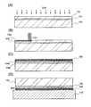
먼저, 단결정 반도체 기판(100)을 준비한다. 그리고, 단결정 반도체 기판(100)의 표면에 이온을 조사하여, 단결정 반도체 기판(100)의 표면으로부터 소정 의 깊이에 이온을 도입하여, 손상 영역(102) 및 단결정 반도체층(104)을 형성한다(도 1(A) 참조). 손상 영역(102)의 형성 방법으로서는, 반도체층에의 불순물 원소의 첨가에 사용되는 방법(이하, 이온 도핑법이라고 한다)이나, 이온화한 가스를 질량 분리하여 선택적으로 반도체층에 주입하는 방법(이하, 이온 주입법이라고 한다) 등을 들 수 있다. 이온 조사는, 형성되는 단결정 반도체층(104)의 두께를 고려하여 행하면 좋다. 단결정 반도체층(104)의 막 두께는 5 nm 내지 500 nm 정도로 하면 좋고, 10 nm 내지 200 nm의 두께로 하면 보다 바람직하다. 이온을 조사할 때의 가속 전압은 상기에 나타내는 바와 같은 단결정 반도체층(104)의 두께를 고려하여 결정할 수 있다.First, a single
단결정 반도체 기판(100)은, 단결정 반도체 재료로 이루어지는 기판이면 특히 한정되지 않지만, 일례로서, 단결정 실리콘 기판을 사용할 수 있다. 그 외에, 게르마늄, 갈륨 비소, 인듐 인 등의 화합물 반도체에 의한 기판을 적용할 수도 있다. 이하에서는, 단결정 반도체 기판(100)으로서 단결정 실리콘 기판을 사용하는 경우에 대하여 설명한다.The single
조사하는 이온으로서는, 불소로 대표되는 할로겐이나, 수소, 헬륨 등의 이온을 들 수 있다. 할로겐의 이온으로서 불소 이온을 조사하는 경우에는, 원료 가스로서 BF3를 사용하면 좋다. 예를 들어, 단결정 반도체 기판(100)으로서 단결정 실리콘 기판을 사용하고, 그 단결정 실리콘 기판에 불소 이온과 같은 할로겐 이온을 조사한 경우에는, 손상 영역(102)에는, 미소한 공동(空洞)이 형성된다. 이것은, 조사된 할로겐 이온이 실리콘 결정 격자 내의 실리콘 원자를 추방(追放)하기 때문이라고 고려된다. 이렇게 하여 형성된 미소한 공동의 체적을 변화시킴으로써, 단결정 실리콘 기판을 분리시킬 수 있다. 구체적으로는, 저온의 열 처리에 의하여 미소한 공동의 체적 변화를 유기(誘起)한다. 또한, 불소 이온을 조사한 후에, 수소 이온을 조사하여 공동 내에 수소를 함유시키도록 하여도 좋다.Examples of ions to be irradiated include halogens represented by fluorine, and ions such as hydrogen and helium. When fluorine ions are irradiated as ions of halogen, BF3 may be used as the source gas. For example, when a single crystal silicon substrate is used as the single
또한, 동일 원자로 이루어지고, 질량수가 상이한 다수의 이온을 조사하여도 좋다. 예를 들어, 수소 이온을 조사하는 경우에는, H+, H2+, H3+이온을 사용하는 것과 함께 H3+이온의 비율을 높이면 좋다. H3+이온의 비율을 높임으로써 조사 효율을 높일 수 있기 때문에, 조사 시간을 단축할 수 있다.It is also possible to irradiate a plurality of ions made of the same atom and having different mass numbers. For example, when hydrogen ions are irradiated, the ratio of H3+ ions may be increased by using H+ , H2+ , and H3+ ions. Since the irradiation efficiency can be increased by increasing the ratio of H3+ ions, irradiation time can be shortened.
다음에, 단결정 반도체층(104)의 표면에 레이저광을 조사한다(도 1(B) 참조). 이에 따라, 단결정 반도체층(104)의 평탄성이 향상되고, 결정성이 회복된 제 1 부분(104a)을 단결정 반도체층(104) 중에 형성할 수 있다. 또한, 절연 표면을 가지는 기판에 단결정 반도체층(104)을 형성한 후의 제 2 부분(104b)에의 레이저광의 조사에 의하여, 단결정 반도체층(104)의 특성을 균일하게 할 수 있다. 또한, 레이저광을 조사할 때, 단결정 반도체 기판(100)을 가열함으로써 레이저광의 조사를 한층 더 효과적으로 행할 수 있다. 이 때의 가열 온도는 100℃ 이상 400℃ 이하로 하면 좋다. 물론, 레이저광을 조사하기 전에 가열 처리를 행하는 구성으로 하여도 좋다.Next, the surface of the single
레이저광의 조사에는, 예를 들어, 연속 발진 레이저(CW 레이저)나, 의사(擬似)적인 CW 레이저(발진 주파수가 10 MHz 이상, 바람직하게는 80 MHz 이상의 펄스 발진 레이저) 등을 사용할 수 있다. 구체적으로는, 연속 발진 레이저로서, Ar 레이저, Kr 레이저, CO2 레이저, YAG 레이저, YVO4 레이저, YLF 레이저, YAlO3 레이저, GdVO4 레이저, Y2O3 레이저, 루비 레이저, 알렉산드라이트 레이저, Ti:사파이어 레이저, 헬륨 카드뮴 레이저 등을 사용할 수 있다. 또한, 의사적인 CW 레이저로서, Ar 레이저, Kr 레이저, 엑시머 레이저, CO2 레이저, YAG 레이저, YVO4 레이저, YLF 레이저, YAlO3 레이저, GdVO4 레이저, Y2O3 레이저, 루비 레이저, 알렉산드라이트 레이저, Ti:사파이어 레이저, 구리 증기 레이저, 또는 금 증기 레이저와 같은 펄스 발진 레이저 등을 사용할 수 있다. 이와 같은 펄스 발진 레이저는, 발진 주파수를 증가시키면, 연속 발진 레이저와 동등으로 취급할 수 있다.For example, a continuous oscillation laser (CW laser) or a pseudo CW laser (pulse oscillation laser having an oscillation frequency of 10 MHz or more, preferably 80 MHz or more) can be used for irradiation with laser light. Specifically, as the continuous oscillation laser, an Ar laser, a Kr laser, a CO2 laser, a YAG laser, a YVO4 laser, a YLF laser, a YAlO3 laser, a GdVO4 laser, a Y2 O3 laser, a ruby laser, : Sapphire laser, helium cadmium laser, or the like can be used. As pseudo-CW lasers, Ar laser, Kr laser, excimer laser, CO2 laser, YAG laser, YVO4 laser, YLF laser, YAlO3 laser, GdVO4 laser, Y2 O3 laser, ruby laser, , A Ti: sapphire laser, a copper vapor laser, or a pulse oscillation laser such as a gold vapor laser. Such a pulse oscillation laser can be treated as equivalent to a continuous oscillation laser by increasing the oscillation frequency.
또한, 본 실시형태에 있어서는, 일례로서 엑시머 레이저를 사용한 레이저광의 조사를 행한다. 구체적으로는, KrF 엑시머 레이저(파장 248 nm)나 XeCl 엑시머 레이저(파장 308 nm) 등을 사용한다.In this embodiment, laser light is irradiated using an excimer laser as an example. Specifically, KrF excimer laser (wavelength 248 nm) or XeCl excimer laser (wavelength 308 nm) is used.
다음에, 레이저광을 조사한 단결정 반도체층(104) 위에 접합층(106)을 형성한다(도 1(C) 참조). 접합층(106)은, 유기 실란 가스를 사용하여 화학 기상 성장법(CVD법)에 의하여 산화규소막으로 형성하면 좋다. 그 외에, 실란 가스를 사용하여 화학 기상 성장법에 의하여 제작되는 산화규소막을 적용할 수도 있다. 화학 기상 성장법을 사용하는 경우에는, 손상 영역(102)으로부터 탈 가스가 일어나지 않는 온도 조건으로 성막할 필요가 있다. 또한, 단결정 반도체 기판(100)으로부터 단결정 반도체층(104)을 분리하는 열처리에는, 성막 온도보다 높은 온도가 적용된다. 또한, 접합층(106)은 절연성 재료로 형성되기 때문에 절연층이라고도 할 수 있다.Next, the
접합층(106)의 표면은 평활하게 형성되고, 친수성을 가진다. 이 접합층(106)으로서는, 산화규소막이 적합하다. 특히, 유기 실란 가스를 사용하여 화학 기상 성장법에 의하여 제작되는 산화규소막이 바람직하다. 유기 실란 가스로서는, 테트라에톡시실란(TEOS)(화학식: Si(OC2H5)4), 트리메틸실란(TMS)(화학식: (CH3)3SiH), 테트라메틸시클로테트라실록산(TMCTS), 옥타메틸시클로테트라실록산(OMCTS), 헥사메틸디실라잔(HMDS), 트리에톡시실란(화학식: SiH(OC2H5)3), 트리스디메틸아미노실란(화학식: SiH(N(CH3)2)3) 등의 규소 함유 화합물을 사용할 수 있다.The surface of the
상기 접합층(106)은 5 nm 내지 500 nm 정도의 두께로 형성된다. 이에 따라, 접합층(106)이 형성된 제 1 부분(104a)의 표면이 평활화되는 것과 함께 접합층(106)의 표면의 평탄성이 향상된다. 또한, 후의 절연 표면을 가지는 기판(110)에도 같은 접합층을 형성할 수 있다. 이와 같이, 접합을 형성하는 면의 한쪽 또는 양쪽 모두를, 유기 실란을 원재료로 하여 성막한 산화규소막으로 함으로써, 접합을 매우 강고한 것으로 할 수 있다.The
또한, 단결정 반도체층(104)과 접합층(106) 사이에 질소 함유 절연층을 형성하는 구성으로 하여도 좋다. 질소 함유 절연층은, 질화규소, 질화산화규소, 산화 질화규소로부터 선택된 하나 또는 다수의 재료를 사용하여 형성할 수 있다. 또한, 질소 함유 절연층은 단층 구조라도 좋고, 적층 구조라도 좋다. 예를 들어, 단결정 반도체층(104) 측으로부터 산화질화규소막, 질화산화규소막을 적층하여 질소 함유 절연층으로 할 수 있다. 질소 함유 절연층은, 알칼리 금속, 알칼리토류 금속과 같은 가동(可動) 이온이나 물 등의 불순물이 단결정 반도체층(104)에 침입하는 것을 방지하기 위하여 형성된다. 또한, 불순물의 침입을 방지할 수 있다면, 질소 함유 절연층 이외의 절연층을 형성하여도 좋다.Further, a nitrogen-containing insulating layer may be formed between the single
여기서, 산화질화규소란, 그의 조성에서 질소보다 산소의 함유량이 많은 것을 가리키며, 예를 들어, 산소가 50 원자% 이상 70 원자% 이하, 질소가 0.5 원자% 이상 15 원자% 이하, 규소가 25 원자% 이상 35 원자% 이하, 수소가 0.1 원자% 이상 10 원자% 이하의 범위로 포함되는 것을 의미한다. 또한, 질화산화규소란, 그의 조성에서 산소보다 질소의 함유량이 많은 것을 가리키며, 예를 들어, 산소가 5 원자% 이상 30 원자% 이하, 질소가 20 원자% 이상 55 원자% 이하, 규소가 25 원자% 이상 35 원자% 이하, 수소가 10 원자% 이상 30 원자% 이하의 범위로 포함되는 것을 의미한다. 다만, 상기 원소 함유량은 러더포드 후방 산란법(RBS: Rutherford Backscattering Spectrometry)이나 수소 전방 산란법(HFS: Hydrogen Forward Scattering)을 사용하여 측정한 경우의 것이다. 또한, 구성 원소의 함유 비율의 합계는 100 원자%를 넘지 않는다.For example, oxygen is contained in an amount of 50 atomic% or more and 70 atomic% or less, nitrogen is contained in an amount of 0.5 atomic% or more and 15 atomic% or less, silicon is contained in an amount of 25 atomic% or less, Or more and 35 atomic% or less, and hydrogen is contained in a range of 0.1 atomic% or more and 10 atomic% or less. For example, oxygen is contained in an amount of 5 atomic% or more and 30 atomic% or less, nitrogen is contained in an amount of 20 atomic% or more and 55 atomic% or less, silicon is 25 atomic or less Or more and 35 atomic% or less, and hydrogen is contained in a range of 10 atomic% or more and 30 atomic% or less. However, the content of the element is measured by Rutherford Backscattering Spectrometry (RBS) or Hydrogen Forward Scattering (HFS). The total content of constituent elements does not exceed 100 atomic%.
또한, 본 실시형태에서는, 이온을 조사한 후에 단결정 반도체층(104)에 레이저광을 조사하고, 그 후, 접합층(106)을 형성하는 구성으로 하고 있지만, 본 발명 은 이것에 한정되지 않는다. 접합의 강도를 일정 이상으로 유지할 수 있으면, 접합층(106)을 형성한 후에 이온을 조사하고, 그 후, 레이저광을 조사하는 구성으로 하여도 좋고, 이온 조사 후에 접합층(106)을 형성하고, 레이저광을 조사하는 구성으로 하여도 좋다. 또한, 질소 함유 절연층을 형성하는 경우에 있어서도, 마찬가지로, 질소 함유 절연층을 이온을 조사하기 전에 형성하여도 좋고, 이온을 조사한 후에 형성하여도 좋다. 이온을 조사하기 전에 형성하는 경우에는, 이온 조사에 의한 단결정 반도체 기판(100)의 표면의 거칠어짐을 방지할 수 있다.In the present embodiment, laser light is irradiated to the single
다음에, 절연 표면을 가지는 기판(110)과 접합층(106)을 밀접시킨다(도 1(D) 참조). 절연 표면을 가지는 기판(110)과 접합층(106)을 밀접시켜 압력을 가함으로써, 수소 결합이나 공유 경합에 의하여 보다 강고한 접합을 형성할 수 있다. 또한, 접합층(106)을 사이에 두고, 절연 표면을 가지는 기판(110)과 단결정 반도체 기판(100)을 접합한 후에는, 가열 처리를 행하는 것이 바람직하다. 가열 처리를 행함으로써 접합 강도를 보다 향상시킬 수 있다.Next, the
양호한 접합을 형성하기 위하여, 접합되는 표면을 활성화시켜도 좋다. 예를 들어, 접합하는 면에 원자 빔 또는 이온 빔을 조사한다. 원자 빔 혹은 이온 빔을 이용하는 경우에는, 아르곤 등의 불활성 가스 원자 빔, 혹은 불활성 가스 이온 빔을 사용할 수 있다. 그 외에, 플라즈마 처리 혹은 라디칼 처리를 행한다. 이와 같은 표면 처리에 의하여 200℃ 내지 400℃ 정도의 저온에서 이종(異種) 재료간의 접합을 형성할 수 있다.In order to form a good junction, the surface to be bonded may be activated. For example, the surface to be bonded is irradiated with an atomic beam or an ion beam. When an atomic beam or an ion beam is used, an inert gas atomic beam such as argon or an inert gas ion beam may be used. In addition, a plasma treatment or a radical treatment is performed. By such surface treatment, it is possible to form a junction between heterogeneous materials at a low temperature of about 200 캜 to 400 캜.
또한, 절연 표면을 가지는 기판(110)으로서는, 알루미노 실리케이트 유리, 알루미노 붕규산 유리, 바륨 붕규산 유리와 같은 전자 공업용에 사용되는 각종 유리 기판, 석영 기판, 세라믹스 기판, 사파이어 기판 등을 사용할 수 있다. 바람직하게는, 유리 기판을 사용하는 것이 좋고, 예를 들어, 제 6 세대(1500 mm×1850 mm), 제 7 세대(1870 mm×2200 mm), 제 8 세대(2200 mm×2400 mm)와 같은 대면적의 마더(mother) 유리 기판을 사용할 수 있다. 대면적의 마더 유리 기판을 절연 표면을 가지는 기판(110)으로서 사용함으로써, 반도체 기판의 대면적화를 실현할 수 있다. 또한, 절연 표면을 가지는 기판(110)은 상기 기판에 한정되지 않는다. 예를 들어, 내열 온도가 프로세스의 최대 온도보다 높으면, 수지 재료로 이루어지는 기판을 사용할 수도 있다.As the
다음에, 가열 처리를 행하여, 손상 영역(102)에서 단결정 반도체 기판(100)으로부터 단결정 반도체층(104)을 분리(박리)한다(도 2(A) 참조). 예를 들어, 400℃ 내지 600℃의 열 처리를 행함으로써, 손상 영역(102)에 형성된 미소한 공동의 체적 변화를 유기하여 분리시킬 수가 있다. 접합층(106)은 절연 표면을 가지는 기판(110)과 접합하여 있으므로, 절연 표면을 가지는 기판(110) 위에는 단결정 반도체층(104)이 잔존하게 된다.Next, the single
절연 표면을 가지는 기판(110)으로서 유리 기판을 사용하는 경우에는, 유리 기판의 변형점 근방, 구체적으로는, 변형점±50℃로 가열을 행하면 좋다. 보다 구체적으로는, 580℃ 이상 680℃ 이하로 행하면 좋다. 또한, 유리 기판은 가열에 의하여 수축하는 성질을 가진다. 그래서, 미리 유리 기판을 변형점 근방, 구체적으로는 변형점±50℃ 정도(혹은 그 이상)로 가열하여 두면, 그 후의 가열 처리에 있 어서의 수축을 억제할 수 있다. 이에 따라, 열 팽장률이 상이한 단결정 반도체층을 접합한 유리 기판에 가열 처리를 행하는 경우라도, 접합된 단결정 반도체층의 유리 기판으로부터의 박리를 방지할 수 있다. 또한, 유리 기판 및 단결정 반도체층의 휨 현상 등의 변형을 방지할 수도 있다. 또한, 상기 가열 처리는, 가열할 때에 수축하는 성질을 가지는 기판을 사용하는 경우라면, 유리 기판에 한정되지 않고 적용할 수 있다.When a glass substrate is used as the
또한, 유리 기판을 사용하는 경우에는, 가열 종료 시의 급속한 냉각을 피하는 것이 바람직하다. 구체적으로는, 2℃/분 이하, 바람직하게는 0.5℃/분 이하, 보다 바람직하게는 0.3℃/분 이하의 속도로 변형점 이하의 온도까지 냉각시키면 좋다. 강온속도를 작게 함으로써, 유리 기판이 수축할 때 생기는 국소적인 응력을 완화할 수 있다. 상기 가열 처리는 대기압 하에서 행하여도 좋고, 감압 하에서 행하여도 좋다. 분위기도 질소 분위기, 산소 분위기 등 적절히 설정할 수 있다.When a glass substrate is used, it is preferable to avoid rapid cooling at the end of heating. Specifically, it may be cooled to a temperature not higher than the strain point at a rate of 2 DEG C / min or less, preferably 0.5 DEG C / min or less, more preferably 0.3 DEG C / min or less. By reducing the cooling rate, it is possible to relax the local stress generated when the glass substrate shrinks. The heat treatment may be performed under atmospheric pressure or under reduced pressure. The atmosphere can also be suitably set in a nitrogen atmosphere, an oxygen atmosphere and the like.
또한, 접합 공정에 관한 가열 처리와, 분리 공정에 관한 가열 처리를 동시에 행할 수도 있다. 이 경우, 한번의 가열 처리로 2가지 공정을 동시에 행할 수 있으므로, 저비용으로 반도체 기판을 제작할 수 있다.Further, the heat treatment for the joining step and the heat treatment for the separation step may be performed at the same time. In this case, since the two steps can be performed simultaneously by one heat treatment, the semiconductor substrate can be manufactured at low cost.
그 후, 단결정 반도체층(104)의 표면에 레이저광을 조사한다(도 2(B) 참조). 이에 따라, 단결정 반도체층(104)의 평탄성을 향상시키고, 단결정 반도체층(104)의 제 2 부분(104b)의 결정성을 회복시킬 수 있다.Thereafter, the surface of the single
두번째의 레이저광 조사에 사용할 수 있는 레이저는 첫번째의 레이저광 조사에 사용할 수 있는 레이저와 마찬가지다. 본 실시형태에서는, 일례로서 엑시머 레 이저를 사용한 레이저광 조사를 행하는 것으로 한다. 구체적으로는, KrF 엑시머 레이저(파장 248 nm)나 XeCl 엑시머 레이저(파장 308 nm) 등을 사용한다.The laser which can be used for the second laser irradiation is the same as the laser which can be used for the first laser irradiation. In this embodiment, laser light irradiation using an excimer laser is performed as an example. Specifically, KrF excimer laser (wavelength 248 nm) or XeCl excimer laser (wavelength 308 nm) is used.
또한, 첫번째의 레이저광 조사에 있어서는, 레이저광의 조사에 의한 온도 상승을, 손상 영역에서의 분리가 생기는 온도 미만으로 억제할 필요가 있다. 한편, 두번째의 레이저광 조사에 있어서는, 단결정 반도체 전체가 용융하지 않는 정도의 강도로 레이저광을 조사할 필요가 있다. 그래서, 레이저광의 강도는 적절히 설정하는 것이 중요하다.Further, in the first laser light irradiation, it is necessary to suppress the temperature rise due to the irradiation of the laser light to a temperature lower than a temperature at which separation in the damaged region occurs. On the other hand, in the second laser light irradiation, it is necessary to irradiate the laser light with an intensity that does not melt the entire single crystal semiconductor. Therefore, it is important to appropriately set the intensity of the laser beam.
이상에 의해, 제 1 부분(104a)과 제 2 부분(104b)에 있어서의 결정성이나 불순물의 활성화율 등의 특성이 대체로 같은 단결정 반도체층(104)을 제작할 수 있다(도 2(C) 참조).Thus, the single
상기의 공정에 의하여 얻어진 단결정 반도체층(104)에 대해서는, 화학적 기계적 연마(Chemical Mechanical Polishing: CMP) 또는 에칭에 의한 평탄화를 행하는 것이 바람직하다. 단결정 반도체층(104)의 평탄성을 향상시킴으로써, 후에 형성하는 반도체 소자의 특성 편차를 억제할 수 있다. 또한, 원하는 특성을 얻을 수 있으면, CMP 공정이나 에칭 공정은 생략하여도 좋다. 또한, 두번째의 레이저광 조사 전에 CMP 공정이나 에칭 공정을 행하는 구성으로 하여도 좋다.The single
또한, 가열이나 레이저광 조사를 재차 행함으로써, 단결정 반도체층(104)의 특성을 향상시켜도 좋다. 또한, 가열 처리할 때의 온도는, 절연 표면을 가지는 기판(110)의 내열 온도를 기준으로 할 수 있다. 절연 표면을 가지는 기판(110)으로서 유리 기판을 사용하는 경우에는, 유리 기판의 변형점을 기준으로 하면 좋다. 구체적으로는, 변형점±50℃(580℃ 이상 680℃ 이하) 정도의 온도로 가열 처리를 행하면 좋다.The characteristics of the single
다음에, 절연 표면을 가지는 기판(110) 측에 접합층(106)을 형성하는 경우에 대하여 도 3(A) 내지 도 3(D)를 사용하여 설명한다. 또한, 도 1(B)에 나타내는 레이저광 조사(첫번째)의 공정까지는 마찬가지이므로, 그에 대한 상세한 설명은 생략한다.Next, the case where the
단결정 반도체층(104)에 레이저광을 조사한 후에, 접합층(106)이 형성된 절연 표면을 가지는 기판(110)과 단결정 반도체 기판(100)을 밀착시킨다(도 3(A) 참조). 구체적으로는, 접합층(106)과 레이저광을 조사한 단결정 반도체층(104)을 밀착시켜 접합시킨다. 또한, 접합층(106)과 절연 표면을 가지는 기판(110)과의 사이에 배리어(barrier) 층을 형성하는 구성으로 하여도 좋다. 배리어 층을 형성함으로써, 단결정 반도체층(104)에의 알칼리 금속이나 알칼리토류 금속과 같은 불순물의 침입을 방지할 수 있다. 절연 표면을 가지는 기판(110)으로부터 단결정 반도체층(104)으로의 불순물의 침입이 문제가 되지 않는 경우에는, 배리어 층을 형성하지 않는 구성으로 하여도 좋다.After the single
배리어 층은, 산화규소, 질화규소, 질화산화규소, 산화질화규소 등으로부터 선택된 하나 또는 다수의 재료를 사용하여 형성할 수 있다. 배리어 층은 단층 구조라도 좋고, 적층 구조라도 좋다. 또한, 불순물의 침입을 방지할 수 있다면, 상기 재료를 사용하여 형성하는 것에 한정되지 않는다. 배리어 층은 절연성 재료로 형성되기 때문에, 절연층이라고 부를 수도 있다.The barrier layer can be formed using one or a plurality of materials selected from silicon oxide, silicon nitride, silicon oxynitride, silicon oxynitride, and the like. The barrier layer may be a single layer structure or a laminated structure. Further, if it is possible to prevent intrusion of impurities, it is not limited to forming using the above-mentioned material. Since the barrier layer is formed of an insulating material, it may be called an insulating layer.
또한, 단결정 반도체층(104)과 접합층(106) 사이에 질소 함유 절연층을 형성하는 구성으로 하여도 좋다. 질소 함유 절연층은, 질화규소, 질화산화규소, 산화질화규소로부터 선택된 하나 또는 다수의 재료를 사용하여 형성할 수 있다. 또한, 질소 함유 절연층은 단층 구조라도 좋고, 적층 구조라도 좋다. 예를 들어, 단결정 반도체층(104) 측으로부터 산화질화규소막, 질화산화규소막을 적층하여 질소 함유 절연층으로 할 수 있다. 질소 함유 절연층은, 알칼리 금속이나 알칼리토류 금속과 같은 가동 이온이나 수분 등의 불순물이 단결정 반도체층(104)에 침입하는 것을 방지하기 위하여 형성된다. 또한, 불순물의 침입을 방지할 수 있다면, 질소 함유 절연층 이외의 절연층을 형성하여도 좋다.Further, a nitrogen-containing insulating layer may be formed between the single
또한, 질소 함유 절연층을 형성하는 경우에는, 그 질소 함유 절연층을 단결정 반도체 기판(100)에 이온을 조사하기 전에 형성하여도 좋고, 이온을 조사한 후에 형성하여도 좋다. 이온을 조사하기 전에 형성하는 경우에는, 이온 조사에 의한 단결정 반도체 기판(100)의 표면의 거칠어짐을 방지할 수 있다.When the nitrogen-containing insulating layer is formed, the nitrogen-containing insulating layer may be formed on the single
그 후, 단결정 반도체 기판(100)을 분리한다(도 3(B) 참조). 단결정 반도체 기판(100)을 분리할 때의 열 처리는 도 2(A)의 경우와 마찬가지로 하여 행할 수 있으므로, 그에 대한 상세한 설명은 생략한다.Thereafter, the single
다음에, 단결정 반도체층(104)의 표면에 레이저광을 조사한다(도 3(C) 참조). 이에 따라, 단결정 반도체층(104)의 평탄성을 향상시키고, 단결정 반도체층(104)의 제 2 부분(104b)의 결정성을 회복시킬 수 있다.Next, the surface of the single
두번째의 레이저광 조사에 사용할 수 있는 레이저는 첫번째의 레이저광 조사 에 사용할 수 있는 레이저와 마찬가지다. 본 실시형태에서는, 일례로서 엑시머 레이저를 사용한 레이저광 조사를 행하는 것으로 한다. 구체적으로는, KrF 엑시머 레이저(파장 248 nm)나 XeCl 엑시머 레이저(파장 308 nm) 등을 사용한다.The laser which can be used for the second laser irradiation is the same as the laser which can be used for the first laser irradiation. In this embodiment, laser light irradiation using an excimer laser is performed as an example. Specifically, KrF excimer laser (wavelength 248 nm) or XeCl excimer laser (wavelength 308 nm) is used.
또한, 첫번째의 레이저광 조사에 있어서는, 레이저광 조사에 의한 온도 상승을, 손상 영역에서의 분리가 생기는 온도 미만으로 억제할 필요가 있다. 한편, 두번째의 레이저광 조사에 있어서는, 단결정 반도체 전체가 용융하지 않는 정도의 강도로 레이저광을 조사할 필요가 있다. 그래서, 레이저광의 강도는 적절히 설정하는 것이 중요하다.In addition, in the first laser light irradiation, it is necessary to suppress the temperature rise due to the laser light irradiation to less than the temperature at which separation in the damaged area occurs. On the other hand, in the second laser light irradiation, it is necessary to irradiate the laser light with an intensity that does not melt the entire single crystal semiconductor. Therefore, it is important to appropriately set the intensity of the laser beam.
이상에 의해, 제 1 부분(104a)과 제 2 부분(104b)에 있어서의 결정성이나 불순물의 활성화율 등의 특성이 대체로 같은 단결정 반도체층(104)을 제작할 수 있다(도 3(D) 참조).Thus, the single
상기의 공정에 의하여 얻어진 단결정 반도체층(104)에 대해서는 화학적 기계적 연마(Chemical Mechanical Polishing: CMP) 또는 에칭에 의한 평탄화를 행하는 것이 바람직하다. 단결정 반도체층(104)의 평탄성을 향상시킴으로써, 후에 형성하는 반도체 소자의 특성 편차를 억제할 수 있다. 또한, 원하는 특성을 얻을 수 있으면, CMP 공정이나 에칭 공정은 생략하여도 좋다. 또한, 두번째의 레이저광 조사 전에 CMP 공정이나 에칭 공정을 행하는 구성으로 하여도 좋다.The single
또한, 가열이나 레이저광 조사를 재차 행함으로써, 단결정 반도체층(104)의 특성을 향상시켜도 좋다. 가열 처리할 때의 온도나 사용할 수 있는 레이저에 대해서는, 상기를 참조할 수 있으므로 여기서는 생략한다.The characteristics of the single
이상에 의해, 단결정 반도체층(104)의 특성을 균일하게 한 반도체 기판을 제공할 수 있다. 이에 따라, 반도체 소자의 특성이 양호한 반도체 장치를 제공할 수 있다.As described above, a semiconductor substrate having uniform characteristics of the single
[실시형태 2][Embodiment 2]
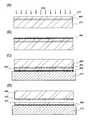
본 실시형태에서는, 본 발명의 반도체 기판의 제조방법의 다른 예에 대하여 도 4 내지 도 6을 참조하여 설명한다. 구체적으로는, 단결정 반도체층을 절연 표면을 가지는 기판에 형성한 후, 레이저광 조사를 행하는 것이다.In this embodiment, another example of the method of manufacturing the semiconductor substrate of the present invention will be described with reference to Figs. 4 to 6. Fig. Specifically, a single crystal semiconductor layer is formed on a substrate having an insulating surface, and laser light irradiation is performed.
먼저, 단결정 반도체 기판(400)을 준비한다. 그리고, 단결정 반도체 기판(400)의 표면에 이온을 조사하여, 단결정 반도체 기판(400)의 표면으로부터 소정의 깊이에 이온을 도입하여, 손상 영역(402) 및 단결정 반도체층(404)을 형성한다(도 4(A) 참조). 손상 영역(402)의 형성 방법으로서는, 이온 도핑법이나 이온 주입법 등을 들 수 있다. 이온 조사는, 형성되는 단결정 반도체층(404)의 두께를 고려하여 행하면 좋다. 상기 단결정 반도체층(404)의 막 두께는 5 nm 내지 500 nm 정도로 하면 좋고, 10 nm 내지 200 nm의 두께로 하면 보다 바람직하다. 이온을 조사할 때의 가속 전압은 상기에서 나타내는 바와 같은 단결정 반도체층(404)의 두께를 고려하여 결정할 수 있다.First, a single
단결정 반도체 기판(400)은, 단결정 반도체 재료로 이루어지는 기판이면 특히 한정되지 않지만, 일례로서, 단결정 실리콘 기판을 사용할 수 있다. 그 외에, 게르마늄, 갈륨 비소, 인듐 인 등의 화합물 반도체에 의한 기판을 적용할 수도 있다. 이하에서는. 단결정 반도체 기판(400)으로서 단결정 실리콘 기판을 사용하는 경우에 대하여 설명한다.Although the single
조사하는 이온으로서는, 불소로 대표되는 할로겐이나, 수소, 헬륨 등의 이온을 들 수 있다. 할로겐의 이온으로서 불소 이온을 조사하는 경우에는, 원료 가스로서 BF3를 사용하면 좋다. 예를 들어, 단결정 반도체 기판(400)으로서 단결정 실리콘 기판을 사용하고, 그 단결정 실리콘 기판에 불소 이온과 같은 할로겐 이온을 조사한 경우에는, 손상 영역(402)에는 미소한 공동이 형성된다. 이것은, 조사시킨 할로겐 이온이 실리콘 결정 격자 내의 실리콘 원자를 추방하기 때문이다. 이렇게 하여 형성된 미소한 공동의 체적을 변화시킴으로써, 단결정 실리콘 기판을 분리시킬 수 있다. 구체적으로는, 저온의 열 처리에 의하여 미소한 공동의 체적 변화를 유기한다. 또한, 불소 이온을 조사한 후에, 수소 이온을 조사하여 공동 내에 수소를 포함시키도록 하여도 좋다.Examples of ions to be irradiated include halogens represented by fluorine, and ions such as hydrogen and helium. When fluorine ions are irradiated as ions of halogen, BF3 may be used as the source gas. For example, when a single crystal silicon substrate is used as the single
또한, 동일 원자로 이루어지고, 질량수가 상이한 다수의 이온을 조사하여도 좋다. 예를 들어, 수소 이온을 조사하는 경우에는, H+, H2+, H3+이온을 사용하는 것과 함께 H3+이온의 비율을 높이면 좋다. H3+이온의 비율을 높임으로써 조사 효율을 높일 수 있기 때문에, 조사 시간을 단축할 수 있다. 또한, 손상 영역을 형성한 후에 가열 처리를 행하는 구성으로 하여도 좋다.It is also possible to irradiate a plurality of ions made of the same atom and having different mass numbers. For example, when hydrogen ions are irradiated, the ratio of H3+ ions may be increased by using H+ , H2+ , and H3+ ions. Since the irradiation efficiency can be increased by increasing the ratio of H3+ ions, irradiation time can be shortened. Further, the heating process may be performed after the damaged region is formed.
다음에, 단결정 반도체층(404) 위에 접합층(406)을 형성한다(도 4(B) 참조). 접합층(406)은, 유기 실란 가스를 사용하여 화학 기상 성장법(CVD법)에 의하여 산 화규소막으로 형성하면 좋다. 그 외에, 실란 가스를 사용하여 화학 기상 성장법에 의하여 제작되는 산화규소막을 적용할 수도 있다. 화학 기상 성장법을 사용하는 경우에는, 손상 영역(402)으로부터 탈 가스가 일어나지 않는 온도 조건으로 성막할 필요가 있다. 또한, 단결정 반도체 기판(400)으로부터 단결정 반도체층(404)을 분리하는 열처리에는, 성막 온도보다 높은 온도가 적용된다. 또한, 접합층(406)은 절연성 재료로 형성되기 때문에, 절연층이라고 부를 수도 있다.Next, a
접합층(406)의 표면은 평활하게 형성되고, 친수성을 가진다. 이 접합층(406)으로서는 산화규소막이 적합하다. 특히, 유기 실란 가스를 사용하여 화학 기상 성장법에 의하여 제작되는 산화규소막이 바람직하다. 유기 실란 가스로서는, 테트라에톡시실란(TEOS)(화학식: Si(OC2H5)4), 트리메틸실란(TMS)(화학식: (CH3)3SiH), 테트라메틸시클로테트라실록산(TMCTS), 옥타메틸시클로테트라실록산(OMCTS), 헥사메틸디실라잔(HMDS), 트리에톡시실란(화학식: SiH(OC2H5)3), 트리스디메틸아미노실란(화학식: SiH(N(CH3)2)3) 등의 규소 함유 화합물을 사용할 수 있다.The surface of the
상기 접합층(406)은 5 nm 내지 500 nm 정도의 두께로 형성된다. 이에 따라, 단결정 반도체층(404)의 표면을 평활화하는 것과 함께 접합층(406)의 표면의 평탄성을 향상시킬 수 있다. 또한, 후의 절연 표면을 가지는 기판(410)에도 같은 접합층을 형성할 수 있다. 이와 같이, 접합을 형성하는 면의 한쪽 혹은 양쪽 모두를 유기 실란을 원재료로 하여 성막한 산화규소막으로 함으로써, 접합을 매우 강고한 것으로 할 수 있다.The
또한, 단결정 반도체층(404)과 접합층(406) 사이에 질소 함유 절연층을 형성하는 구성으로 하여도 좋다. 질소 함유 절연층은, 질화규소, 질화산화규소, 산화질화규소로부터 선택된 하나 또는 다수의 재료를 사용하여 형성할 수 있다. 또한, 질소 함유 절연층은 단층 구조라도 좋고, 적층 구조라도 좋다. 예를 들어, 단결정 반도체층(404) 측으로부터 산화질화규소막, 질화산화규소막을 적층하여 질소 함유 절연층으로 할 수 있다. 질소 함유 절연층은, 알칼리 금속, 알칼리토류 금속과 같은 가동 이온이나 물 등의 불순물이 단결정 반도체층(404)에 침입하는 것을 방지하기 위하여 형성된다. 또한, 불순물의 침입을 방지할 수 있다면, 질소 함유 절연층 이외의 절연층을 형성하여도 좋다.Further, a nitrogen-containing insulating layer may be formed between the single
또한, 본 실시형태에서는, 이온을 조사한 후에 접합층(406)을 형성하는 구성으로 하고 있지만, 본 발명은 이것에 한정되지 않는다. 접합의 강도를 일정 이상으로 유지할 수 있으면, 접합층(406)을 형성한 후에 이온을 조사하는 구성으로 하여도 좋다. 또한, 질소 함유 절연층을 형성하는 경우에 대해서도 마찬가지로, 질소 함유 절연층을 이온을 조사하기 전에 형성하여도 좋고, 이온을 조사한 후에 형성하여도 좋다. 이온을 조사하기 전에 형성하는 경우에는, 이온 조사에 의한 단결정 반도체 기판(400)의 표면의 거칠어짐을 방지할 수 있다.In this embodiment, the
다음에, 절연 표면을 가지는 기판(410)과 접합층(406)을 밀접시킨다(도 4(C) 참조). 절연 표면을 가지는 기판(410)과 접합층(406)을 밀접시켜 압력을 가함으로써, 수소 결합이나 공유 경합에 의하여 보다 강고한 접합을 형성할 수 있다. 또 한, 접합층(406)을 사이에 두고, 절연 표면을 가지는 기판(410)과 단결정 반도체 기판(400)을 접합한 후에는, 가열 처리를 행하는 것이 바람직하다. 가열 처리를 행함으로써 접합 강도를 더욱 향상시킬 수 있다.Next, the
양호한 접합을 형성하기 위하여, 접합되는 표면을 활성화시켜도 좋다. 예를 들어, 접합하는 면에 원자 빔 혹은 이온 빔을 조사한다. 원자 빔 혹은 이온 빔을 이용하는 경우에는, 아르곤 등의 불활성 가스 원자 빔, 혹은 불활성 가스 이온 빔을 사용할 수 있다. 그 외에, 플라즈마 처리 혹은 라디칼 처리를 행한다. 이와 같은 표면 처리에 의하여, 200℃ 내지 400℃ 정도의 저온으로 이종(異種) 재료간의 접합을 형성할 수 있다.In order to form a good junction, the surface to be bonded may be activated. For example, the surface to be bonded is irradiated with an atomic beam or an ion beam. When an atomic beam or an ion beam is used, an inert gas atomic beam such as argon or an inert gas ion beam may be used. In addition, a plasma treatment or a radical treatment is performed. By such a surface treatment, it is possible to form a junction between different kinds of materials at a low temperature of about 200 캜 to 400 캜.
또한, 절연 표면을 가지는 기판(410)으로서는, 알루미노 실리케이트 유리, 알루미노 붕규산 유리, 바륨 붕규산 유리와 같은 전자 공업용에 사용되는 각종 유리 기판, 석영 기판, 세라믹스 기판, 사파이어 기판 등을 사용할 수 있다. 바람직하게는, 유리 기판을 사용하는 것이 좋고, 예를 들어, 제 6 세대(1500 mm×1850 mm), 제 7 세대(1870 mm×2200 mm), 제 8 세대(2200 mm×2400 mm)와 같은 대면적의 마더 유리 기판을 사용할 수 있다. 대면적의 마더 유리 기판을 절연 표면을 가지는 기판(410)으로서 사용함으로써, 반도체 기판의 대면적화를 실현할 수 있다. 또한, 절연 표면을 가지는 기판(410)은 상기의 기판에 한정되지 않는다. 예를 들어, 내열 온도가 프로세스의 최대 온도보다 높으면, 수지 재료로 이루어지는 기판을 사용할 수도 있다. 또한, 본 실시형태에서, 절연 표면을 가지는 기판(410)을 통과하여 단결정 반도체층(404)에 레이저광을 조사하는 관계상, 절연 표면을 가지는 기 판(410)은 레이저광을 투과하는 재료에 의하여 형성된 것일 필요가 있다.As the
다음에, 가열 처리를 행하고, 손상 영역(402)에서 단결정 반도체층(404)을 단결정 반도체 기판(400)으로부터 분리한다(도 4(D) 참조). 예를 들어, 400℃ 내지 600℃의 열 처리를 행함으로써, 손상 영역(402)에 형성된 미소한 공동의 체적 변화를 유기하여 분리시킬 수가 있다. 접합층(406)은 절연 표면을 가지는 기판(410)과 접합하여 있기 때문에, 절연 표면을 가지는 기판(410) 위에는 단결정 반도체층(404)이 잔존하게 된다.Next, a heating process is performed to separate the single
절연 표면을 가지는 기판(410)으로서 유리 기판을 사용하는 경우에는, 유리 기판의 변형점 근방, 구체적으로는, 변형점±50℃로 가열을 행하면 좋다. 보다 구체적으로는, 580℃ 이상 680℃ 이하로 행하면 좋다. 또한, 유리 기판은 가열에 의하여 수축하는 성질을 가진다. 따라서, 미리 유리 기판을 변형점 근방, 구체적으로는 변형점±50℃ 정도(혹은 그 이상)로 가열하여 두면, 그 후의 가열 처리에 있어서의 수축을 억제할 수 있다. 이에 따라, 열 팽장률이 상이한 단결정 반도체층을 접합한 유리 기판에 가열 처리를 행하는 경우라도, 유리 기판으로부터의 단결정 반도체층의 박리를 방지할 수 있다. 또한, 유리 기판 및 단결정 반도체층의 휨 현상 등의 변형을 방지할 수도 있다. 또한, 상기 가열 처리는, 가열 시에 수축하는 성질을 가지는 기판을 사용하는 경우라면, 유리 기판에 한정되지 않고 적용할 수 있다.When a glass substrate is used as the
또한, 유리 기판을 사용하는 경우에는, 가열 종료시의 급속한 냉각을 피하는 것이 바람직하다. 구체적으로는, 2℃/분 이하, 바람직하게는 0.5℃/분 이하, 보다 바람직하게는 0.3℃/분 이하의 속도로 변형점 이하의 온도까지 냉각시키면 좋다. 강온(降溫) 속도를 작게 함으로써, 유리 기판이 수축할 때 생기는 국소적인 응력을 완화할 수 있다. 상기 가열 처리는 대기압 하에서 행하여도 좋고, 감압 하에서 행하여도 좋다. 분위기도 질소 분위기, 산소 분위기 등 적절히 설정할 수 있다.When a glass substrate is used, it is desirable to avoid rapid cooling at the end of heating. Specifically, it may be cooled to a temperature not higher than the strain point at a rate of 2 DEG C / min or less, preferably 0.5 DEG C / min or less, more preferably 0.3 DEG C / min or less. By reducing the cooling rate, it is possible to alleviate the local stress generated when the glass substrate shrinks. The heat treatment may be performed under atmospheric pressure or under reduced pressure. The atmosphere can also be suitably set in a nitrogen atmosphere, an oxygen atmosphere and the like.
또한, 접합 공정에 관한 가열 처리와, 조사 공정에 관한 가열 처리를 동시에 행할 수도 있다. 이 경우, 한번의 가열 처리로 2가지 공정을 동시에 행할 수 있으므로, 저비용으로 반도체 기판을 제작할 수 있다.Further, the heat treatment for the joining step and the heat treatment for the irradiation step may be performed at the same time. In this case, since the two steps can be performed simultaneously by one heat treatment, the semiconductor substrate can be manufactured at low cost.
다음에, 단결정 반도체층(404)의 뒷면으로부터 레이저광을 조사한다(도 5(A) 참조). 이에 따라, 결정성이 회복된 단결정 반도체층(404)의 제 1 부분(404a)을 형성할 수 있다.Next, laser light is irradiated from the back surface of the single crystal semiconductor layer 404 (see Fig. 5 (A)). Thus, the
레이저광의 조사에는, 예를 들어, 연속 발진 레이저(CW 레이저)나, 의사적인 CW 레이저(발진 주파수가 10 MHz 이상, 바람직하게는 80 MHz 이상인 펄스 발진 레이저) 등을 사용할 수 있다. 구체적으로는, 연속 발진 레이저로서, Ar 레이저, Kr 레이저, CO2 레이저, YAG 레이저, YVO4 레이저, YLF 레이저, YAlO3 레이저, GdVO4 레이저, Y2O3 레이저, 루비 레이저, 알렉산드라이트 레이저, Ti:사파이어 레이저, 헬륨 카드뮴 레이저 등을 사용할 수 있다. 또한, 의사적인 CW 레이저로서, Ar 레이저, Kr 레이저, 엑시머 레이저, CO2 레이저, YAG 레이저, YVO4 레이저, YLF 레이저, YAlO3 레이저, GdVO4 레이저, Y2O3 레이저, 루비 레이저, 알렉산드라이트 레이저, Ti:사파이어 레이저, 구리 증기 레이저, 또는 금 증기 레이저와 같은 펄스 발진 레 이저 등을 사용할 수 있다. 이와 같은 펄스 발진 레이저는, 발진 주파수를 증가시키면, 연속 발진 레이저와 동등(同等)으로 취급할 수 있다.For example, a continuous oscillation laser (CW laser) or a pseudo-CW laser (pulse oscillation laser having an oscillation frequency of 10 MHz or more, preferably 80 MHz or more) can be used for irradiation with laser light. Specifically, as the continuous oscillation laser, an Ar laser, a Kr laser, a CO2 laser, a YAG laser, a YVO4 laser, a YLF laser, a YAlO3 laser, a GdVO4 laser, a Y2 O3 laser, a ruby laser, : Sapphire laser, helium cadmium laser, or the like can be used. As pseudo-CW lasers, Ar laser, Kr laser, excimer laser, CO2 laser, YAG laser, YVO4 laser, YLF laser, YAlO3 laser, GdVO4 laser, Y2 O3 laser, ruby laser, , A Ti: sapphire laser, a copper vapor laser, or a pulse oscillation laser such as a gold vapor laser. Such a pulse oscillation laser can be treated as equivalent to a continuous oscillation laser by increasing the oscillation frequency.
또한, 본 실시형태에서는, 일례로서 엑시머 레이저를 사용한 레이저광의 조사를 행한다. 구체적으로는, KrF 엑시머 레이저(파장 248 nm)나 XeCl 엑시머 레이저(파장 308 nm) 등을 사용한다.In this embodiment, laser light is irradiated using an excimer laser as an example. Specifically, KrF excimer laser (wavelength 248 nm) or XeCl excimer laser (wavelength 308 nm) is used.
다음에, 단결정 반도체층(404)의 표면으로부터 레이저광을 조사한다(도 5(B) 참조). 이에 따라, 단결정 반도체층(404)의 평탄성이 향상되고, 단결정 반도체층(404)의 제 2 부분(404b)의 결정성을 회복시킬 수 있다. 또한, 두번째의 레이저광 조사에 사용할 수 있는 레이저는 첫번째의 레이저광 조사에 사용할 수 있는 레이저와 마찬가지이다.Next, laser light is irradiated from the surface of the single crystal semiconductor layer 404 (see FIG. 5 (B)). Thus, the flatness of the single
이상에 의해, 제 1 부분(404a)과 제 2 부분(404b)에 있어서 결정성이나 불순물의 활성화율 등의 특성이 대체로 같은 단결정 반도체층(404)을 제작할 수 있다(도 5(C) 참조).Thus, the single
상기의 공정에 의하여 얻어진 단결정 반도체층(404)에 대해서는 화학적 기계적 연마(Chemical Mechanical Polishing: CMP) 또는 에칭에 의한 평탄화를 행하는 것이 바람직하다. 단결정 반도체층(404)의 평탄성을 향상시킴으로써, 후에 형성하는 반도체 소자의 특성 편차를 억제할 수 있다. 또한, 원하는 특성을 얻을 수 있으면, CMP 공정이나 에칭 공정은 생략하여도 좋다. 또한, 첫번째의 레이저광 조사 전이나 두번째의 레이저광 조사 전에 CMP 공정이나 에칭 공정을 행하는 구성으로 하여도 좋다.The single
또한, 가열이나 레이저광 조사를 재차 행함으로써, 단결정 반도체층(404)의 특성을 향상시켜도 좋다. 또한, 가열 처리할 때의 온도는, 절연 표면을 가지는 기판(410)의 내열 온도를 기준으로 할 수 있다. 절연 표면을 가지는 기판(410)으로서 유리 기판을 사용하는 경우에는, 유리 기판의 변형점을 기준으로 하면 좋다. 구체적으로는, 변형점±50℃(580℃ 이상 680℃ 이하) 정도의 온도로 가열 처리를 행하면 좋다.The characteristics of the single
또한, 본 실시형태에서는, 먼저 뒷면 측(절연 표면을 가지는 기판 측)으로부터 레이저광을 조사하고, 다음에 표면 측으로부터 레이저광을 조사하였지만, 본 발명은 이것에 한정되지 않는다. 먼저 표면 측으로부터 레이저광을 조사하고, 다음에 뒷면 측으로부터 레이저광을 조사하는 구성으로 하여도 좋다. 또한, 단결정 반도체층(404)의 분리 전에 뒷면으로부터 레이저광의 조사를 행하고, 단결정 반도체층(404)의 분리 후에 표면으로부터 레이저광의 조사를 행하는(표면 조사) 구성으로 하여도 좋다. 이 경우에는, 뒷면 조사에 의한 열을 단결정 반도체층(404)의 분리에 사용하여, 레이저광 조사 공정과 분리 공정을 동시에 행할 수도 있다. 이 때에는, 표면 조사의 레이저광의 강도에 비하여 뒷면 조사의 레이저광의 강도를 크게 하는 것이 바람직하다.In the present embodiment, laser light is first irradiated from the back side (substrate side having the insulating surface), and then the laser light is irradiated from the front side, but the present invention is not limited to this. The laser light may be irradiated from the front side first and then the laser light may be irradiated from the rear side. Furthermore, laser light may be irradiated from the back surface before separation of the single
다음에, 절연 표면을 가지는 기판(410) 측에 접합층(406)을 형성하는 경우에 대하여 도 6(A) 내지 도 6(E)를 사용하여 설명한다. 먼저, 단결정 반도체 기판(400)을 준비한다. 그리고, 단결정 반도체 기판(400)의 표면에 이온을 조사하여, 단결정 반도체 기판(400)의 표면으로부터 소정의 깊이에 이온을 도입하여, 손 상 영역(402) 및 단결정 반도체층(404)을 형성한다(도 6(A) 참조). 그의 상세한 것에 대해서는, 단결정 반도체 기판(400) 측에 접합층(406)을 형성하는 경우와 마찬가지이므로, 여기서는 생략한다.Next, a case where the
다음에, 절연 표면을 가지는 기판(410) 위에 접합층(406)을 형성한다(도 6(B) 참조). 접합층(406)은, 유기 실란 가스를 사용하여 화학 기상 성장법(CVD법)에 의하여 산화규소막으로 형성하면 좋다. 접합층(406)은 절연성 재료로 형성되기 때문에, 절연층이라고 부를 수도 있다. 또한, 접합층(406)과 절연 표면을 가지는 기판(410) 사이에 배리어 층을 형성하는 구성으로 하여도 좋다. 배리어 층을 형성함으로써, 단결정 반도체층(404)에의 알칼리 금속이나 알칼리토류 금속과 같은 불순물의 침입을 방지할 수 있다. 절연 표면을 가지는 기판(410)으로부터 단결정 반도체층(404)에의 불순물의 침입이 문제가 되지 않는 경우에는, 배리어 층을 형성하지 않는 구성으로 하여도 좋다. 또한, 그의 상세한 것에 대해서는, 실시형태 1 등의 기재를 참조할 수 있다.Next, a
다음에, 단결정 반도체층(404)과 접합층(406)을 밀접시킨다(도 6(C) 참조). 단결정 반도체층(404)과 접합층(406)을 밀접시켜 압력을 가함으로써, 수소 결합이나 공유 경합에 의하여 보다 강고한 접합을 형성할 수 있다. 또한, 접합층(406)을 사이에 두고, 절연 표면을 가지는 기판(410)과 단결정 반도체 기판(400)을 접합한 후에는, 가열 처리를 행하는 것이 바람직하다. 가열 처리를 행함으로써 접합 강도를 더욱 향상시킬 수 있다.Next, the single
또한, 단결정 반도체층(404)과 접합층(406) 사이에 질소 함유 절연층을 형성 하는 구성으로 하여도 좋다. 질소 함유 절연층은, 질화규소, 질화산화규소, 산화질화규소로부터 선택된 하나 또는 다수의 재료를 사용하여 형성할 수 있다. 또한, 질소 함유 절연층은 단층 구조라도 좋고, 적층 구조라도 좋다. 예를 들어, 단결정 반도체층(404) 측으로부터 산화질화규소막, 질화산화규소막을 적층하여 질소 함유 절연층으로 할 수 있다. 질소 함유 절연층은, 알칼리 금속, 알칼리토류 금속과 같은 가동 이온이나 수분 등의 불순물이 단결정 반도체층(404)에 침입하는 것을 방지하기 위하여 형성된다. 또한, 불순물의 침입을 방지할 수 있다면, 질소 함유 절연층 이외의 절연층을 형성하여도 좋다.Further, a nitrogen-containing insulating layer may be formed between the single
또한, 질소 함유 절연층을 형성하는 경우에는, 질소 함유 절연층을 단결정 반도체 기판(400)에 이온을 조사하기 전에 형성하여도 좋고, 이온을 조사한 후에 형성하여도 좋다. 이온을 조사하기 전에 형성하는 경우에는, 이온 조사에 의한 단결정 반도체 기판(400)의 표면의 거칠어짐을 방지할 수 있다.In the case of forming the nitrogen-containing insulating layer, the nitrogen-containing insulating layer may be formed before the ions are irradiated to the single
다음에, 단결정 반도체 기판(400)을 분리한다(도 6(D) 참조). 단결정 반도체 기판(400)을 분리할 때의 상세한 것에 대해서는, 실시형태 1 등의 기재를 참조할 수 있다.Next, the single
그 후, 도 5의 경우와 마찬가지로 단결정 반도체층(404)의 뒷면 및 표면으로부터 레이저광을 조사한다. 이상에 의해, 제 1 부분(404a)과 제 2 부분(404b)에 있어서 결정성이나 불순물의 활성화율 등이 대체로 같은 단결정 반도체층(404)을 제작할 수 있다(도 6(E) 참조).Thereafter, as in the case of FIG. 5, laser light is irradiated from the back surface and the surface of the single
상기의 공정에 의하여 얻어진 단결정 반도체층(404)에 대해서도 화학적 기계 적 연마(Chemical Mechanical Polishing: CMP) 또는 에칭에 의한 평탄화를 행하는 것이 바람직하다. 단결정 반도체층(404)의 평탄성을 향상시킴으로써, 후에 형성하는 반도체 소자의 특성 편차를 억제할 수 있다. 또한, 원하는 특성을 얻을 수 있으면, CMP 공정이나 에칭 공정은 생략하여도 좋다. 또한, 두번째의 레이저광 조사 전에 CMP 공정이나 에칭 공정을 행하는 구성으로 하여도 좋다.The single
또한, 가열이나 레이저광 조사를 재차 함으로써, 단결정 반도체층(404)의 특성을 향상시켜도 좋다. 가열 처리 시의 온도나 사용할 수 있는 레이저에 대해서는, 상기를 참조할 수 있으므로 여기서는 생략한다.Further, the characteristics of the single
이상에 의해, 단결정 반도체층(404)의 특성을 균일하게 한 반도체 기판을 제공할 수 있다. 이에 따라, 반도체 소자의 특성이 양호한 반도체 장치를 제공할 수 있다.As described above, a semiconductor substrate having uniform characteristics of the single
또한, 본 실시형태는 실시형태 1과 적절히 조합하여 사용할 수 있다.The present embodiment can be used in combination with
[실시형태 3][Embodiment 3]
본 실시형태에서는, 본 발명의 반도체 장치의 제조방법의 일례에 대하여 도 7 내지 도 10을 참조하여 설명한다. 또한, 본 실시형태에서는, 반도체 장치의 일례로서 액정 표시장치를 들어 설명하지만, 본 발명의 반도체 장치는 액정 표시장치에 한정되지 않는다.In this embodiment, an example of a method for manufacturing a semiconductor device of the present invention will be described with reference to Figs. 7 to 10. Fig. Although the liquid crystal display device is described as an example of the semiconductor device in the present embodiment, the semiconductor device of the present invention is not limited to the liquid crystal display device.
먼저, 본 실시형태 1이나 실시형태 2 등에 나타낸 방법을 사용하여, 절연 표면을 가지는 기판 위에 단결정 반도체층을 형성한다(도 7(A) 참조). 여기서는, 절연 표면을 가지는 기판(700) 위에 배리어 층(702), 접합층(704), 단결정 반도체 층(706)을 순차로 형성한 구성을 사용하여 설명하지만, 본 발명은 이것에 한정되지 않는다. 다음에, 단결정 반도체층(706) 및 접합층(704)을 원하는 형상으로 패터닝하여, 섬 형상의 단결정 반도체층을 형성한다.First, a single crystal semiconductor layer is formed on a substrate having an insulating surface by using the method shown in
또한, 패터닝할 때의 에칭 가공으로서는, 플라즈마 에칭(드라이 에칭), 웨트 에칭 중 어느 것이나 채용하여도 좋지만, 대면적 기판을 처리하는 데에는, 플라즈마 에칭이 적합하다. 또한, 에칭 가스로서는, CF4, NF3, Cl2, BCl3 등의 불소계 또는 염소계 가스를 사용하고, He나 Ar 등의 불활성 가스를 적절히 가하여도 좋다. 또한, 대기압 방전의 에칭 가공을 적용하면, 국소적인 방전 가공도 가능하여, 기판의 전면에 마스크 층을 형성할 필요는 없다.As the etching for patterning, any of plasma etching (dry etching) and wet etching may be employed, but plasma etching is suitable for processing a large area substrate. As the etching gas, a fluorine-based or chlorine-based gas such as CF4 , NF3 , Cl2 or BCl3 may be used and an inert gas such as He or Ar may be appropriately added. Further, by applying the etching process of the atmospheric pressure discharge, it is also possible to perform local discharge processing, and it is not necessary to form the mask layer on the entire surface of the substrate.
단결정 반도체층(706) 및 접합층(704)을 패터닝한 후에는, 스레시홀드 전압을 제어하기 위하여, 붕소, 알루미늄, 갈륨 등의 p형 불순물을 첨가하면 좋다. 예를 들어, p형 불순물로서 붕소를 5×1017cm-3이상 1×1018cm-3이하의 농도로 첨가할 수 있다.After the single
절연 표면을 가지는 기판(700) 위에는, 배리어 층(702)으로서 질화규소층과 산화규소층이 적층 구조로 형성되어 있다. 배리어 층(702)을 형성함으로써, 단결정 반도체층(706)의 가동 이온에 의한 오염을 방지할 수 있다. 또한, 질화규소층 대신에 질화산화규소층, 질화알루미늄층, 질화산화알루미늄층을 적용하여도 좋다.On the
다음에, 섬 형상의 단결정 반도체층을 덮는 게이트 절연층(708)을 형성한다(도 7(B) 참조). 또한, 여기서는 편의상, 패터닝에 의하여 형성한 섬 형상의 단결 정 반도체층을 각각 단결정 반도체층(710), 단결정 반도체층(712), 단결정 반도체층(714)이라고 부르기로 한다. 게이트 절연층(708)은, 플라즈마 CVD법 또는 스퍼터링법 등을 사용하여 두께를 10 nm 이상 150 nm 이하 정도로 하여 규소를 함유하는 절연막으로 형성한다. 구체적으로는, 질화규소, 산화규소, 산화질화규소, 질화산화규소로 대표되는 규소의 산화물 재료 또는 질화물 재료 등의 재료로 형성하면 좋다. 또한, 게이트 절연층(708)은 단층 구조라도 좋고, 적층 구조라도 좋다. 또한, 단결정 반도체층과 게이트 절연층 사이에 막 두께 1 nm 이상 100 nm 이하 정도, 바람직하게는, 1 nm 이상 10 nm 이하, 보다 바람직하게는 2 nm 이상 5 nm 이하의 얇은 산화규소막을 형성하여도 좋다. 또한, 낮은 온도에서 누설 전류가 적은 게이트 절연층을 형성하기 위하여, 아르곤 등의 희가스 원소를 반응 가스에 포함시켜도 좋다.Next, a
다음에, 게이트 절연층(708) 위에 게이트 전극층으로서 사용하는 제 1 도전막과 제 2 도전막을 적층하여 형성한다. 제 1 도전막의 막 두께는 20 nm 이상 100 nm 이하 정도, 제 2 도전막의 막 두께는 100 nm 이상 400 nm 이하 정도로 하면 좋다. 또한, 제 1 도전막 및 제 2 도전막은 스퍼터링법, 증착법, CVD법 등의 수단으로 형성할 수 있다. 제 1 도전막 및 제 2 도전막은, 탄탈(Ta), 텅스텐(W), 티탄(Ti), 몰리브덴(Mo), 알루미늄(Al), 구리(Cu), 크롬(Cr), 및 네오디뮴(Nd) 중에서 선택된 원소, 또는 상기 원소를 주성분으로 하는 합금 재료 혹은 화합물 재료 등을 사용하여 형성하면 좋다. 또한, 제 1 도전막 및 제 2 도전막으로서, 인 등의 불순물 원소를 도핑한 다결정 규소막으로 대표되는 반도체막이나 AgPdCu 합금 등을 사용하여도 좋다. 또한, 본 실시형태에서는, 2층 구조를 사용하여 설명하지만, 본 발명은 이것에 한정되지 않는다. 3층 이상의 적층 구조로 하여도 좋고, 단층 구조라도 좋다.Next, a first conductive film and a second conductive film to be used as a gate electrode layer are formed on the
다음에, 포토리소그래피법을 사용하여, 레지스트 재료로 된 마스크(716a), 마스크(716b), 마스크(716c), 마스크(716d), 및 마스크(716e)를 형성한다. 그리고, 상기 마스크를 사용하여 제 1 도전막 및 제 2 도전막을 원하는 형상으로 가공하여, 제 1 게이트 전극층(718a), 제 1 게이트 전극층(718b), 제 1 게이트 전극층(718c), 제 1 게이트 전극층(718d), 제 1 도전층(718e), 도전층(720a), 도전층(720b), 도전층(720c), 도전층(720d), 도전층(720e)을 형성한다(도 7(C) 참조).Next, a
여기서, ICP(Inductively Coupled Plasma: 유도 결합형 플라즈마) 에칭법을 사용하고, 에칭 조건(코일형 전극에 인가되는 전력량, 기판 측의 전극에 인가되는 전력량, 기판 측의 전극 온도 등)을 적절히 조절함으로써, 원하는 테이퍼 형상이 되도록 에칭할 수 있다. 또한, 마스크의 형상에 의해 테이퍼 각도 등을 제어할 수도 있다. 또한, 에칭용 가스로서는, Cl2, BCl3, SiCl4 혹은 CCl4등을 대표로 하는 염소계 가스, CF4, SF6 혹은 NF3 등을 대표로 하는 불소계 가스, 또는 O2를 적절히 사용할 수 있다. 본 실시형태에서는, CF4, Cl2, O2로 이루어지는 에칭용 가스를 사용하여 제 2 도전막의 에칭을 행하고, 연속하여, CF4, Cl2로 이루어지는 에칭용 가스를 사용하여 제 1 도전막을 에칭한다.Here, by using an ICP (Inductively Coupled Plasma) etching method and appropriately adjusting the etching conditions (the amount of power applied to the coil-shaped electrode, the amount of power applied to the electrode on the substrate side, the electrode temperature of the substrate, etc.) , So that a desired taper shape can be obtained. Further, the taper angle and the like can be controlled by the shape of the mask. As the etching gas, a chlorine-based gas typified by Cl2 , BCl3 , SiCl4 or CCl4 , a fluorine-based gas typified by CF4 , SF6 or NF3 , or O2 can be suitably used . In this embodiment, the second conductive film is etched using an etching gas composed of CF4 , Cl2 , and O2 , and the first conductive film is etched successively by using an etching gas composed of CF4 and Cl2 do.
다음에, 마스크(716a), 마스크(716b), 마스크(716c), 마스크(716d), 및 마스 크(716e)를 사용하여 도전층(720a), 도전층(720b), 도전층(720c), 도전층(720d), 도전층(720e)을 원하는 형상으로 가공한다. 이 때, 도전층을 형성하는 제 2 도전막과, 제 1 게이트 전극층 및 제 1 도전층을 형성하는 제 1 도전막과의 선택비가 높은 에칭 조건으로 에칭한다. 이 에칭에 의하여, 제 2 게이트 전극층(722a), 제 2 게이트 전극층(722b), 제 2 게이트 전극층(722c), 제 2 게이트 전극층(722d), 및 제 2 도전층(722e)을 형성한다. 본 실시형태에서는, 제 2 게이트 전극층 및 제 2 도전층도 테이퍼 형상을 가지지만, 그 테이퍼 각도는 제 1 게이트 전극층(718a), 제 1 게이트 전극층(718b), 제 1 게이트 전극층(718c), 제 1 게이트 전극층(718d), 및 제 1 도전층(718e)이 가지는 테이퍼 각도보다 크다. 또한, 본 명세서에서, 테이퍼 각도란, 대상물의 저면(底面)과 측면으로 이루어지는 각도를 말하는 것으로 한다. 따라서, 테이퍼 각도가 90도인 경우, 도전층은 저면에 대하여 수직인 측면을 가지게 된다. 테이퍼 각도를 90도 미만으로 함으로써, 적층되는 막의 피복성이 향상되기 때문에, 결함을 저감할 수 있게 된다. 또한, 본 실시형태에서는, 제 2 게이트 전극층 및 제 2 도전층을 형성하기 위한 에칭용 가스로서 Cl2, SF6, O2를 사용한다.Next, the
이상의 공정에 의하여, 주변 구동회로 영역(780)에 게이트 전극층(724a) 및 게이트 전극층(724b)을 형성할 수 있고, 화소 영역(790)에 게이트 전극층(724c), 게이트 전극층(724d), 및 게이트 전극층(724e)을 형성할 수 있다(도 7(D) 참조). 또한, 마스크(716a), 마스크(716b), 마스크(716c), 마스크(716d), 및 마스크(716e) 는 상기 공정 후에 제거된다.The
다음에, 게이트 전극층(724a), 게이트 전극층(724b), 게이트 전극층(724c), 게이트 전극층(724d)을 마스크로 하여, n형을 부여하는 불순물 원소를 첨가하여, 제 1 n형 불순물 영역(726a), 제 1 n형 불순물 영역(726b), 제 1 n형 불순물 영역(728a), 제 1 n형 불순물 영역(728b), 제 1 n형 불순물 영역(730a),,제 1 n형 불순물 영역(730b), 제 1 n형 불순물 영역(730c)을 형성한다(도 8(A) 참조). 본 실시형태에서는, 불순물 원소를 포함하는 도핑 가스로서 포스핀(PH3)을 사용하여 도핑을 행한다. 여기서는, 제 1 n형 불순물 영역에, n형을 부여하는 불순물 원소인 인(P)이 1×10¹⁷/cm3 내지 5×10¹⁸/cm3정도의 농도로 함유되도록 한다.Next, an impurity element imparting n-type conductivity is added using the
다음에, 단결정 반도체층(710)과, 단결정 반도체층(714)의 일부를 덮는 마스크(732a), 마스크(732b), 마스크(732c)를 형성한다. 그리고, 마스크(732a), 마스크(732b), 마스크(732c) 및 제 2 게이트 전극층(722b)을 마스크로 하여, n형을 부여하는 불순물 원소를 첨가한다. 이것에 의해, 제 2 n형 불순물 영역(734a), 제 2 n형 불순물 영역(734b), 제 3 n형 불순물 영역(736a), 제 3 n형 불순물 영역(736b), 제 2 n형 불순물 영역(740a), 제 2 n형 불순물 영역(740b), 제 2 n형 불순물 영역(740c), 제 3 n형 불순물 영역(742a), 제 3 n형 불순물 영역(742b), 제 3 n형 불순물 영역(742c), 제 3 n형 불순물 영역(742d)이 형성된다. 본 실시형태에서는, 불순물 원소를 포함하는 도핑 가스로서 포스핀(PH3)을 사용하여 도핑을 행한다. 여기서는, 제 2 n형 불순물 영역에, n형을 부여하는 불순물 원소인 인(P)이 5 ×10¹⁹/cm3 내지 5×10²⁰/cm3정도의 농도로 함유되도록 한다. 제 3 n형 불순물 영역(736a), 제 3 n형 불순물 영역(736b)에는, 제 3 n형 불순물 영역(742a), 제 3 n형 불순물 영역(742b), 제 3 n형 불순물 영역(742c), 제 3 n형 불순물 영역(742d)과 같은 정도 혹은 약간 높은 농도로, n형을 부여하는 불순물 원소가 첨가된다. 또한, 채널 형성 영역(738), 채널 형성 영역(744a) 및 채널 형성 영역(744b)이 형성된다(도 8(B) 참조).Next, a
제 2 n형 불순물 영역은 고농도 불순물 영역이고, 소스 또는 드레인으로서 기능한다. 한편, 제 3 n형 불순물 영역은 저농도 불순물 영역이고, 이른바 LDD(Lightly Doped Drain) 영역이 된다. 제 3 n형 불순물 영역(736a), 제 3 n형 불순물 영역(736b)은, 제 1 게이트 전극층(718b)과 겹치는 영역에 형성되어 있다. 이에 따라, 소스 또는 드레인 근방의 전계를 완화하여, 핫 캐리어(hot carrier)에 의한 온)ON) 전류의 열화(劣化)를 방지할 수 있다. 한편, 제 3 n형 불순물 영역(742a), 제 3 n형 불순물 영역(742b), 제 3 n형 불순물 영역(742c), 제 3 n형 불순물 영역(742d)은 게이트 전극층(724c), 게이트 전극층(724d)과 겹치지 않고, 오프 전류를 저감하는 효과가 있다.The second n-type impurity region is a high concentration impurity region and functions as a source or a drain. On the other hand, the third n-type impurity region is a low concentration impurity region and is a so-called LDD (Lightly Doped Drain) region. The third n-type impurity region 736a and the third n-type impurity region 736b are formed in a region overlapping the first
다음에, 마스크(732a), 마스크(732b), 마스크(732c)를 제거하고, 단결정 반도체층(712), 단결정 반도체층(714)을 덮는 마스크(746a), 마스크(746b)를 형성한다. 그리고, 마스크(746a), 마스크(746b), 게이트 전극층(724a)을 마스크로 하여, p형을 부여하는 불순물 원소를 첨가한다. 이것에 의해, 제 1 p형 불순물 영 역(748a), 제 1 p형 불순물 영역(748b), 제 2 p형 불순물 영역(750a), 제 2 p형 불순물 영역(750b)이 형성된다. 본 실시형태에서는, 불순물 원소를 포함하는 도핑 가스로서 디보란(B2H6)을 사용하여 도핑을 행한다. 여기서는, 제 1 p형 불순물 영역 및 제 2 p형 불순물 영역에, p형을 부여하는 불순물 원소인 붕소(B)가 1×10²⁰/cm3 내지 5×10²¹/cm3정도의 농도로 함유되도록 한다. 또한, 채널 형성 영역(752)이 형성된다(도 8(C) 참조).Next, the
제 1 p형 불순물 영역은 고농도 불순물 영역이고, 소스 또는 드레인으로서 기능한다. 한편, 제 2 p형 불순물 영역은, 저농도 불순물 영역이고, 이른바 LDD(Lightly Doped Drain) 영역이 된다.The first p-type impurity region is a high concentration impurity region and functions as a source or a drain. On the other hand, the second p-type impurity region is a low-concentration impurity region and is a so-called LDD (Lightly Doped Drain) region.
그 후, 마스크(746a)와 마스크(746b)를 제거한다. 마스크를 제거한 후, 게이트 전극층의 측면을 덮도록 절연막을 형성하여도 좋다. 이 절연막은 플라즈마 CVD법이나 감압 CVD법(LPCVD법)을 사용하여 형성할 수 있다. 또한, 불순물 원소를 활성화하기 위하여, 가열 처리, 강광 조사, 레이저광 조사 등을 행하여도 좋다.Thereafter, the
다음에, 게이트 전극층, 및 게이트 절연층을 덮는 층간절연층을 형성한다. 본 실시형태에서는, 절연막(754)과 절연막(756)의 적층 구조로 한다(도 9(A) 참조). 절연막(754)으로서 질화산화규소막을 막 두께 100 nm로 형성하고, 절연막(756)으로서 산화질화규소막을 막 두께 900 nm로 형성한다. 본 실시형태에서는, 2층의 적층 구조로 하지만, 단층 구조라도 좋고, 3층 이상의 적층 구조로 하여도 좋다. 본 실시형태에서는, 절연막(754) 및 절연막(756)을 플라즈마 CVD법을 사용하여 연 속적으로 형성한다. 또한, 절연막(754) 및 절연막(756)은 상기 재료에 한정되지 않는다.Next, an interlayer insulating layer covering the gate electrode layer and the gate insulating layer is formed. In this embodiment, a laminated structure of an insulating
절연막(754) 및 절연막(756)은, 이 외에, 산화규소나 질화규소, 산화 알루미늄, 질화 알루미늄(AlN), 산화질화 알루미늄(AlON), 질소 함유량이 산소 함유량보다 많은 질화산화 알루미늄(AlNO), 다이아몬드 라이크 카본(diamond-like carbon: DLC), 질소 함유 탄소막, 그 외의 무기 절연성 재료를 포함하는 물질로부터 선택된 재료를 사용하여 형성할 수 있다. 또한, 실록산 수지를 사용하여도 좋다. 실록산 수지란, Si-O-Si 결합을 포함하는 수지를 말한다. 실록산은 규소(Si)와 산소(O)와의 결합으로 골격 구조가 구성된다. 치환기로서, 적어도 수소를 함유하는 유기기(예를 들어, 알킬기, 아릴기)가 사용된다. 치환기로서, 플루오로기를 사용하여도 좋다. 또한, 치환기로서, 적어도 수소를 함유하는 유기기와 플루오로기를 사용하여도 좋다. 또한, 폴리이미드, 아크릴 폴리머, 폴리아미드, 폴리이미드 아미드, 벤조시클로부텐계 재료, 폴리실라잔 등의 유기 절연성 재료를 사용할 수도 있다.The insulating
다음에, 레지스트 재료로 이루어지는 마스크를 사용하여 절연막(754), 절연막(756), 게이트 절연층(708)에 단결정 반도체층 및 게이트 전극층에 도달하는 콘택트 홀(개구부)을 형성한다. 에칭은, 사용하는 재료의 선택비에 따라 한번 행하여도 좋고, 여러 번 행하여도 좋다. 본 실시형태에서는, 산화질화규소막인 절연막(756)과, 질화산화규소막인 절연막(754) 및 게이트 절연층(708)과의 사이에서 높은 선택비가 취해질 수 있는 조건으로 제 1 에칭을 행하고, 절연막(756)을 제거한다. 다음에, 제 2 에칭에 의하여, 절연막(754) 및 게이트 절연층(708)을 제거하여 소스 또는 드레인에 도달하는 개구부를 형성한다.Next, a single-crystal semiconductor layer and a contact hole (opening) reaching the gate electrode layer are formed in the insulating
그 후, 개구부를 덮도록 도전막을 형성하고, 그 도전막을 에칭한다. 이것에 의해, 각 소스 영역 또는 드레인 영역의 일부와 각각 전기적으로 접속하는 소스 전극층 또는 드레인 전극층(758a), 소스 전극층 또는 드레인 전극층(758b), 소스 전극층 또는 드레인 전극층(760a), 소스 전극층 또는 드레인 전극층(760b), 소스 전극층 또는 드레인 전극층(762a), 소스 전극층 또는 드레인 전극층(762b)을 형성한다. 소스 전극층 또는 드레인 전극층에는, 알루미늄(Al), 탄탈(Ta), 티탄(Ti), 몰리브덴(Mo), 텅스텐(W), 네오디뮴(Nd), 크롬(Cr), 니켈(Ni), 백금(Pt), 금(Au), 은(Ag), 구리(Cu), 마그네슘(Mg), 스칸듐(Sc), 코발트(Co), 니켈(Ni), 아연(Zn), 니오븀(Nb), 규소(Si), 인(P), 붕소(B), 비소(As), 갈륨(Ga), 인듐(In), 주석(Sn)으로부터 선택된 하나 또는 다수의 원소, 또는 상기 원소를 성분으로서 함유하는 화합물이나 합금 재료(예를 들어, 인듐 주석 산화물(ITO), 인듐 아연 산화물(IZO), 산화규소를 첨가한 인듐 주석 산화물(ITSO), 산화아연(ZnO), 알루미늄-네오디뮴(Al-Nd), 마그네슘-은(Mg-Ag) 등), 또는 이들 화합물을 조합한 물질 등이 사용된다. 그 외에도, 실리사이드(예를 들어, 알루미늄-규소, 몰리브덴-규소, 니켈 실리사이드)나, 질소를 함유하는 화합물(예를 들어, 질화티탄, 질화탄탈, 질화몰리브덴), 인(P) 등의 불순물 원소를 도핑한 규소(Si) 등을 사용하여도 좋다.Thereafter, a conductive film is formed so as to cover the opening, and the conductive film is etched. As a result, a source electrode layer or a
이상의 공정으로, 주변 구동회로 영역(780)에 p채널형 박막트랜지스터(764) 및 n채널형 박막트랜지스터(766)가 형성되고, 화소 영역(790)에 n채널형 박막트랜지스터(768) 및 용량 배선(770)이 형성된다(도 9(B) 참조).In the above process, the p-channel
다음에, 제 2 층간절연층으로서 절연막(772)을 형성한다. 절연막(772)으로서는, 산화규소, 질화규소, 산화질화규소, 질화산화규소, 산화 알루미늄, 질화 알루미늄(AlN), 산화질화 알루미늄(AlON), 질소 함유량이 산소 함유량보다 많은 질화산화 알루미늄(AlNO), 다이아몬드 라이크 카본(DLC), 질소 함유 탄소막, PSG(인 유리), BPSG(붕소 인 유리), 알루미나막, 폴리실라잔, 그 외의 무기 절연성 재료를 포함하는 물질로부터 선택된 재료로 형성할 수 있다. 또한, 실록산 수지를 사용하여도 좋다. 폴리이미드, 아크릴 폴리머, 폴리아미드, 폴리이미드 아미드, 벤조시클로부텐계 수지 등의 유기 절연성 재료를 사용할 수도 있다.Next, an insulating
본 실시형태에서, 제 2 층간절연층은 평탄화를 위하여 형성한다. 평탄화를 위한 절연층으로서는, 내열성 및 절연성이 높고, 또한, 단차(段差)를 평탄화하는 능력이 높은 것이 요구되기 때문에, 스핀 코팅법으로 대표되는 도포법을 사용하여 형성하는 것이 바람직하다.In this embodiment, the second interlayer insulating layer is formed for planarization. Since the insulating layer for planarization is required to have a high heat resistance and insulation property and a high ability to planarize the step difference, it is preferable to form the insulating layer using a coating method typified by a spin coating method.
다음에, 화소 영역(790)의 절연막(772)에 콘택트 홀을 형성하고, 화소 전극층(774)을 형성한다(도 9(C) 참조). 화소 전극층(774)은, 인듐 주석 산화물(ITO), 산화 인듐에 산화아연(ZnO)을 혼합한 IZO(Indium Zinc Oxide), 산화 인듐에 산화규소(SiO2)을 혼합한 도전성 재료, 유기 인듐, 유기 주석, 산화 텅스텐을 함유하는 인듐 산화물, 산화 텅스텐을 함유하는 인듐 아연 산화물, 산화 티탄을 함유하는 인듐 산화물, 산화 티탄을 함유하는 인듐 주석 산화물, 또는 텅스텐(W), 몰리브덴(Mo), 지르코늄(Zr), 하프늄(Hf), 바나듐(V), 니오븀(Nb), 탄탈(Ta), 크롬(Cr), 코발 트(Co), 니켈(Ni), 티탄(Ti), 백금(Pt), 알루미늄(Al), 구리(Cu), 은(Ag) 등의 금속 또는 그의 합금 혹은 그의 금속 질화물을 사용하여 형성할 수 있다.Next, a contact hole is formed in the insulating
또한, 화소 전극층(774)으로서는, 도전성 고분자(도전성 폴리머라고도 한다)를 포함하는 도전성 조성물을 사용할 수도 있다. 도전성 조성물은, 박막에 있어서의 시트 저항이 10000 Ω/sq. 이하인 것이 바람직하다. 또한, 광 투과성을 가지는 화소 전극층으로서 도전성 조성물의 박막을 형성하는 경우에는, 파장 550 nm에 있어서의 투과율이 70% 이상인 것이 바람직하다. 또한, 포함되는 도전성 고분자의 저항률이 0.1 Ω·cm 이하인 것이 바람직하다.As the
상기의 도전성 고분자로서는, 이른바 π 전자공액계 도전성 고분자를 사용할 수 있다. 예를 들어, 폴리아닐린 및 그의 유도체, 폴리피롤 및 그의 유도체, 폴리티오펜 및 그의 유도체, 또는 그들의 공중합체 등을 들 수 있다.As the above-mentioned conductive polymer, a so-called pi electron conjugated conductive polymer can be used. For example, polyaniline and derivatives thereof, polypyrrole and derivatives thereof, polythiophene and derivatives thereof, and copolymers thereof.
공액계 도전성 고분자의 구체적인 예로서는, 폴리피롤, 폴리(3-메틸피롤), 폴리(3-부틸피롤), 폴리(3-옥틸피롤), 폴리(3-데실피롤), 폴리(3,4-디메틸피롤), 폴리(3,4-디부틸피롤), 폴리(3-하이드록시피롤), 폴리(3-메틸-4-하이드록시피롤), 폴리(3-메톡시피롤), 폴리(3-에톡시피롤), 폴리(3-옥톡시피롤), 폴리(3-카르복실피롤), 폴리(3-메틸-4-카르복실피롤), 폴리(N-메틸피롤), 폴리티오펜, 폴리(3-메틸티오펜), 폴리(3-부틸티오펜), 폴리(3-옥틸티오펜), 폴리(3-데실티오펜), 폴리(3-도데실티오펜), 폴리(3-메톡시티오펜), 폴리(3-에톡시티오펜), 폴리(3-옥톡시티오펜), 폴리(3-카르복실티오펜), 폴리(3-메틸-4-카르복실티오펜), 폴리(3,4-에틸렌디옥시티오펜), 폴리아닐린, 폴리(2-메틸아닐린), 폴리(2-옥틸아닐린), 폴리(2-이소부 틸아닐린), 폴리(3-이소부틸아닐린), 폴리(2-아닐린술폰산), 폴리(3-아닐린술폰산) 등을 들 수 있다.Specific examples of the conjugated system conductive polymer include polypyrrole, poly (3-methylpyrrole), poly (3-butylpyrrole), poly (3-octylpyrrole) Poly (3-hydroxypyrrole), poly (3-methoxypyrrole), poly (3-hydroxypyrrole) Poly (3-methyl-4-carboxylpyrrole), poly (N-methylpyrrole), polythiophene, poly (3-methylthiophene), poly (3-butylthiophene), poly (3-octylthiophene) Poly (3-ethylthiophene), poly (3-ethoxythiophene), poly (3-ethoxythiophene) Poly (3-isobutyl aniline), poly (2-aniline sulfone), poly (2-hexyl aniline) Acid), and poly (3-anilinesulfonic acid).
상기의 도전성 고분자를 단독으로 사용하여도 좋고, 막의 특성을 조정하기 위하여 유기 수지를 첨가하여 사용하여도 좋다.The conductive polymer may be used singly or an organic resin may be added to adjust the characteristics of the film.
또한, 유기 수지는 도전성 고분자와 상용(相溶) 또는 혼합 분산 가능하면, 열 경화성 수지라도 좋고, 열 가소성 수지라도 좋고, 광 경화성 수지라도 좋다. 예를 들어, 폴리에틸렌 테레프탈레이트, 폴리부틸렌 테레프탈레이트, 폴리에틸렌 나프탈레이트 등의 폴리에스테르계 수지, 폴리이미드, 폴리아미드 이미드 등의 폴리이미드계 수지, 폴리아미드 6, 폴리아미드 66, 폴리아미드 12, 폴리아미드 11 등의 폴리아미드 수지, 폴리불화 비닐리덴, 폴리비닐 플루오르화물, 폴리테트라플루오로에틸렌, 에틸렌테트라플루오로에틸렌 코폴리머, 폴리클로로트리플루오로에틸렌 등의 불소 수지, 폴리비닐 알코올, 폴리비닐 에테르, 폴리비닐 부티랄, 폴리초산비닐, 폴리염화비닐 등의 비닐 수지, 에폭시 수지, 크실렌 수지, 아라미드 수지, 폴리우레탄계 수지, 폴리우레아계 수지, 멜라민 수지, 페놀계 수지, 폴리에테르, 아크릴계 수지, 및 이들의 공중합체 등을 들 수 있다.Further, the organic resin may be thermosetting resin, thermoplastic resin, or photocurable resin as long as it is compatibilized or mixed and dispersible with the conductive polymer. For example, polyester resins such as polyethylene terephthalate, polybutylene terephthalate and polyethylene naphthalate, polyimide resins such as polyimide and polyamide imide, polyamide 6, polyamide 66, polyamide 12, Polyamide resins such as polyamide 11, polyvinylidene fluoride, polyvinyl fluoride, polytetrafluoroethylene, ethylene tetrafluoroethylene copolymer and polychlorotrifluoroethylene, polyvinyl alcohol, polyvinyl ether Epoxy resin, xylene resin, aramid resin, polyurethane resin, polyurea resin, melamine resin, phenol resin, polyether, acrylic resin and the like, such as polyvinyl butyral, polyvinyl acetate and polyvinyl chloride; And copolymers thereof.
또한, 도전성 조성물에 억셉터성의 도펀트나 도너성의 도펀트를 도핑함으로써, 공액 도전성 고분자의 산화환원 전위를 변화시켜, 전기 전도도를 조절하여도 좋다.The conductivity may be adjusted by changing the redox potential of the conjugated conductive polymer by doping an acceptor dopant or a donor dopant to the conductive composition.
억셉터성의 도펀트로서는, 할로겐 화합물, 루이스산(Lewis acid), 프로톤산(protonic acid), 유기 시아노 화합물, 유기금속 화합물 등을 사용할 수 있다. 할로겐 화합물로서는, 염소, 브롬, 요오드, 염화 요오드, 브롬화 요오드, 불화 요오드 등을 들 수 있다. 루이스산으로서는, 5불화 인, 5불화 비소, 5불화 안티몬, 3불화 붕소, 3염화 붕소, 3취화 붕소 등을 들 수 있다. 프로톤산으로서는, 염산, 황산, 질산, 인산, 불화붕산, 불화수소산, 과염소산 등의 무기산과, 유기 카르복실산, 유기 술폰산 등의 유기산을 들 수 있다. 유기 시아노 화합물로서는, 공액 결합에 2개 이상의 시아노기를 포함하는 화합물을 사용할 수 있다. 예를 들어, 테트라시아노에틸렌, 산화 테트라시아노에틸렌, 테트라시아노벤진, 테트라시아노퀴노디메탄, 테트라시아노아자나프탈렌 등을 들 수 있다.As the acceptor dopant, a halogen compound, Lewis acid, protonic acid, an organic cyano compound, an organometallic compound and the like can be used. Examples of the halogen compound include chlorine, bromine, iodine, iodine chloride, iodine bromide, and iodine fluoride. Examples of the Lewis acid include phosphorus pentafluoride, arsenic pentafluoride, antimony pentafluoride, boron trifluoride, boron trichloride, and boron trihalide. Examples of the proton acids include inorganic acids such as hydrochloric acid, sulfuric acid, nitric acid, phosphoric acid, fluoroboric acid, hydrofluoric acid and perchloric acid, and organic acids such as organic carboxylic acids and organic sulfonic acids. As the organic cyano compound, a compound containing two or more cyano groups in a conjugated bond can be used. Examples thereof include tetracyanoethylene, tetracyanoethylene oxide, tetracyano benzene, tetracyanoquinodimethane, tetracyanoazanaphthalene, and the like.
도너성의 도펀트로서는, 알칼리 금속, 알칼리토류 금속, 3급 아민 화합물 등을 들 수 있다.Examples of donor-type dopants include alkali metals, alkaline earth metals, and tertiary amine compounds.
상술한 바와 같이, 도전성 조성물을 물 또는 유기 용제(알코올계 용제, 케톤계 용제, 에스테르계 용제, 탄화수소계 용제, 방향족 용제 등)에 용해시켜, 도포법, 코팅법, 액적 토출법(잉크젯법이라고도 한다), 인쇄법 등의 습식법에 의하여 화소 전극층(774)이 되는 박막을 형성할 수 있다.As described above, the conductive composition may be dissolved in water or an organic solvent (alcohol solvent, ketone solvent, ester solvent, hydrocarbon solvent, aromatic solvent, etc.), and the coating method, coating method, droplet discharging method A thin film to be the
다음에, 화소 전극층(774) 및 절연막(772)을 덮도록 배향막이라고 불리는 절연층(1002)을 형성한다(도 10(B) 참조). 절연층(1002)은 스크린 인쇄법이나, 오프셋 인쇄법을 사용하여 형성할 수 있다. 또한, 도 10은 반도체 장치의 평면도 및 단면도를 나타내는 것으로, 도 10(A)는 반도체 장치의 평면도, 도 10(B)는 도 10(A)의 C-D선에 있어서의 단면도이다. 반도체 장치에는, 외부 단자 접속 영역(776), 봉지(封止) 영역(778), 주변 구동회로 영역(780), 화소 영역(790)이 형성 된다.Next, an insulating
절연층(1002)을 형성한 후, 러빙 처리를 행한다. 배향막으로서 기능하는 절연층(1006)에 대해서도 절연층(1002)과 마찬가지로 형성할 수 있다.After the insulating
그 후, 대향 기판(1000)과, 절연 표면을 가지는 기판(700)을 시일(seal)재(1014) 및 스페이서(1016)을 사이에 두고 접합하고, 그의 공극(空隙)에 액정층(1004)을 마련한다. 또한, 대향 기판(1000)에는, 배향막으로서 기능하는 절연층(1006), 대향 전극으로서 기능하는 도전층(1008), 컬러 필터로서 기능하는 착색층(1010), 편광자(1012)(편광판이라고도 한다) 등이 제공되어 있다. 또한, 절연 표면을 가지는 기판(700)에도 편광자(1018)(편광판)을 제공하지만, 본 발명은 이것에 한정되지 않는다. 예를 들어, 반사형의 액정 표시장치에 있어서는, 편광자는 한쪽에 마련하면 된다.Thereafter, the
이어서, 화소 영역과 전기적으로 접속되어 있는 단자 전극층(1020)에, 이방성 도전체층(1022)을 통하여 FPC(1024)를 접속한다. FPC(1024)는 외부로부터의 신호를 전달하는 역할을 한다. 상기의 공정에 의하여, 액정 표시장치를 제작할 수 있다.Then, the
본 발명에서는, 단결정 반도체층(706)의 표면(도면에 있어서의 상방의 면) 및 뒷면(도면에 있어서의 하방의 면)에 레이저광을 조사함으로써, 단결정 반도체층(706)의 특성을 균일하게 하고 있다. 이에 따라, 화소 영역 및 주변 구동화로 영역에 특성이 우수한 반도체 소자를 제작할 수 있다. 구체적으로는, 단결정 반도 체층을 사용한 트랜지스터에 있어서, 드레인 전류(Id)-게이트 전압(Vg) 곡선을 매끄럽게(smooth) 할 수 있다. 즉, 우수한 스위칭 특성의 트랜지스터를 얻을 수 있다.In the present invention, the characteristics of the single
본 발명과 같은 우수한 특성의 트랜지스터를 사용함으로써, 각종 회로의 신뢰성을 향상시킬 수 있다. 예를 들어, 주변 구동회로에 있어서는, 동작 전압을 작게 할 수 있기 때문에 고속 동작 및 저소비전력을 실현할 수 있다. 또한, 화소 영역의 회로에 있어서는, 인가 전압에 대한 전류의 변화가 단조(單調)하기 때문에 고속 동작 및 저소비전력에 더하여 정확한 계조의 표현을 실현할 수 있다. 즉, 본 발명에 의하여, 뛰어난 화질 및 우수한 동영상 특성을 가지는 반도체 장치를 제공할 수 있다. 또한, 주변 구동회로 등을 소형화, 박형화할 수 있기 때문에, 반도체 장치의 두께 및 프레임 부분의 면적을 저감하여, 표시 영역을 유효하게 활용한 반도체 장치를 저비용으로 제공할 수 있다.By using transistors having excellent characteristics as in the present invention, reliability of various circuits can be improved. For example, in the peripheral driving circuit, since the operating voltage can be reduced, high-speed operation and low power consumption can be realized. Further, in the circuit of the pixel region, since the change of the current with respect to the applied voltage is monotonous, accurate gradation expression can be realized in addition to high-speed operation and low power consumption. That is, according to the present invention, a semiconductor device having excellent image quality and excellent moving image characteristics can be provided. In addition, since the peripheral driving circuit and the like can be downsized and thinned, the thickness of the semiconductor device and the area of the frame portion can be reduced, and a semiconductor device that effectively utilizes the display region can be provided at low cost.
또한, 본 실시형태에서는 액정 표시장치를 제작하는 방법에 대하여 설명하였지만, 본 발명은 이것에 한정되지 않는다. 본 실시형태는 실시형태 1 및 실시형태 2를 적절히 조합하여 사용할 수 있다.Although the method of manufacturing the liquid crystal display device has been described in the present embodiment, the present invention is not limited thereto. This embodiment mode can be used by appropriately combining
[실시형태 4][Embodiment 4]
본 실시형태에는, 본 발명에 따른 발광 소자를 가지는 반도체 장치(일렉트로루미네슨스(EL) 표시장치)에 대하여 설명한다. 또한, 주변회로 영역이나 화소 영역 등에 사용되는 트랜지스터의 제작방법은 실시형태 3을 참조할 수 있으므로, 그에 대한 상세한 설명은 생략한다.In this embodiment, a semiconductor device (electroluminescence (EL) display device) having a light emitting element according to the present invention will be described. A method of manufacturing a transistor used in a peripheral circuit region, a pixel region, and the like can be described with reference to Embodiment Mode 3, and a detailed description thereof will be omitted.
또한, 발광 소자를 가지는 반도체 장치에는, 하면 방사, 상면 방사, 양면 방사 중 어느 방식이라도 사용된다. 본 실시형태에서는, 하면 방사 방식을 사용한 반도체 장치에 대하여 도 11(A) 및 도 11(B)를 사용하여 설명하지만, 본 발명이 이것에 한정되는 것은 아니다.In the semiconductor device having a light emitting element, any of bottom emission, top emission, and double emission can be used. In the present embodiment, a semiconductor device using a bottom surface emission method will be described with reference to Figs. 11 (A) and 11 (B), but the present invention is not limited thereto.
도 11(A) 및 도 11(B)의 반도체 장치는 하방(도면 중의 점선 화살표의 방향)으로 광을 방사한다. 여기서, 도 11(A)는 반도체 장치의 평면도이고, 도 11(B)는 도 11(A)의 E-F선에 있어서의 단면도이다. 도 11(A) 및 도 11(B)에서, 반도체 장치는 외부 단자 접속 영역(1130), 봉지 영역(1132), 구동회로 영역(1134), 화소 영역(1136)을 가진다.The semiconductor device of Figs. 11 (A) and 11 (B) emits light downward (in the direction of a dotted arrow in the figure). 11 (A) is a plan view of the semiconductor device, and FIG. 11 (B) is a cross-sectional view taken along line E-F of FIG. 11 (A). 11A and 11B, the semiconductor device has an external
도 11(A) 및 도 11(B)에 나타내는 반도체 장치는 소자 기판(1100), 절연막(1102), 박막트랜지스터(1150), 박막트랜지스터(1152), 박막트랜지스터(1154), 박막트랜지스터(1156), 발광 소자(1160), 절연층(1168), 충전재(1170), 시일재(1172), 배선층(1174), 단자 전극층(1176), 이방성 도전층(1178), FPC(1180), 봉지 기판(1190)에 의하여 구성되어 있다. 또한, 발광 소자(1160)는 제 1 전극층(1162)과 발광층(1164)과 제 2 전극층(1166)을 포함한다.The semiconductor device shown in Figs. 11A and 11B includes an
제 1 전극층(1162)으로서는, 발광층(1164)으로부터 방사하는 광을 투과할 수 있도록 광 투과성을 가지는 도전성 재료를 사용한다. 한편, 제 2 전극층(1166)으로서는, 발광층(1164)으로부터 방사하는 광을 반사할 수 있는 도전성 재료를 사용한다.As the
제 1 전극층(1162)으로서는, 산화 텅스텐을 함유하는 인듐 산화물, 산화 텅 스텐을 함유하는 인듐 아연 산화물, 산화 티탄을 함유하는 인듐 산화물, 산화 티탄을 함유하는 인듐 주석 산화물 등을 사용할 수 있다. 물론, 인듐 주석 산화물(ITO), 인듐 아연 산화물(IZO), 산화규소를 첨가한 인듐 주석 산화물(ITSO) 등을 사용하여도 좋다.As the
또한, 제 1 전극층(1162)으로서는, 도전성 고분자(도전성 폴리머라고도 한다)를 포함하는 도전성 조성물을 사용할 수도 있다. 또한, 상세한 것에 대해서는 실시형태 3을 참조할 수 있으므로, 여기서는 생략한다.As the
제 2 전극층(1166)으로서는, 티탄(Ti), 텅스텐(W), 니켈(Ni), 금(Au), 백금(Pt), 은(Ag), 구리(Cu), 탄탈(Ta), 몰리브덴(Mo), 알루미늄(Al), 마그네슘(Mg), 칼슘(Ca), 리튬(Li) 및 그들의 합금으로 이루어지는 도전막 등을 사용할 수 있다. 가시광의 영역에서 반사성이 높은 물질을 사용하는 것이 좋고, 본 실시형태에서는, 알루미늄막을 사용하는 것으로 한다.As the
또한, 상면 반사, 양면 반사의 각 방식을 사용하는 경우에는, 전극층의 설계를 적절히 변경시키면 된다. 구체적으로는, 상면 방사의 경우에는, 반사성을 가지는 재료를 사용하여 제 1 전극층(1162)을 형성하고, 광 투과성을 가지는 재료를 사용하여 제 2 전극층(1166)을 형성한다. 양면 반사의 경우에는, 광 투과성을 가지는 재료를 사용하여 제 1 전극층(1162) 및 제 2 전극층(1166)을 형성하면 된다. 또한, 하면 반사, 상면 반사에 있어서는, 광 투과성을 가지는 재료를 사용하여 한쪽 전극층을 형성하고, 광 투과성을 가지는 재료와 광 반사성을 가지는 재료의 적층 구조로 다른 쪽 전극층을 형성하는 구성으로 하여도 좋다. 전극층에 사용할 수 있는 재료는 하면 반사의 경우와 마찬가지이므로, 여기서는 생략한다.Further, in the case of using each of the top reflection type and the double-side reflection type, the design of the electrode layer may be appropriately changed. Specifically, in the case of top surface radiation, a
또한, 광 투과성을 가지지 않는 금속막과 같은 재료라도, 막 두께를 작게(5 nm 이상 30 nm 이하 정도) 함으로써, 광을 투과하는 상태로 할 수 있다. 이에 따라, 상술한 광 반사성 재료를 사용하여, 광을 투과하는 전극층을 제작할 수도 있다.Further, even in the case of a material such as a metal film having no light transmission property, light can be transmitted through a small thickness (about 5 nm or more and 30 nm or less). Accordingly, an electrode layer that transmits light can also be fabricated using the above-described light-reflective material.
봉지 기판(1190)에 컬러 필터(착색층)를 형성하는 구성으로 하여도 좋다. 컬러 필터(착색층)는 증착법이나 액적 토출법에 의하여 형성할 수 있다. 또한, 색 변환층을 사용하는 구성이라도 좋다.And a color filter (colored layer) may be formed on the sealing
본 발명에서는, 단결정 반도체층의 표면(도면에 있어서의 상방의 면) 및 뒷면(도면에 있어서의 하방의 면)에 레이저광을 조사함으로써 단결정 반도체층의 특성을 균일하게 하고 있다. 이에 따라, 화소 영역 및 주변 구동회로 영역에 특성이 우수한 반도체 소자를 제작할 수 있다. 구체적으로는, 단결정 반도체층을 사용한 트랜지스터에 있어서 드레인 전류(Id)-게이트 전압(Vg) 곡선을 매끄럽게 할 수 있다. 즉, 우수한 스위칭 특성의 트랜지스터를 얻을 수 있다.In the present invention, the characteristics of the single crystal semiconductor layer are made uniform by irradiating laser light on the surface (the upper surface in the drawing) and the back surface (the lower surface in the drawing) of the single crystal semiconductor layer. Thus, a semiconductor device having excellent characteristics in the pixel region and the peripheral driver circuit region can be manufactured. Specifically, the drain current (Id ) -gate voltage (Vg ) curve can be smoothed in a transistor using a single crystal semiconductor layer. That is, a transistor having excellent switching characteristics can be obtained.
본 발명과 같은 우수한 특성의 트랜지스터를 사용함으로써, 각종 회로의 신뢰성을 향상시킬 수 있다. 예를 들어, 주변 구동회로에 있어서는, 동작 전압을 작게 할 수 있기 때문에 고속 동작 및 저소비전력을 실현할 수 있다. 또한, 화소 영역의 회로에 있어서는, 인가 전압에 대한 전류의 변화가 단조(單調)하기 때문에 고속 동작 및 저소비전력에 더하여 정확한 계조의 표현을 실현할 수 있다. 즉, 본 발명에 의하여, 뛰어난 화질 및 우수한 동영상 특성을 가지는 반도체 장치를 제공할 수 있다. 또한, 주변 구동회로 등을 소형화, 박형화할 수 있기 때문에, 반도체 장치의 두께 및 프레임 부분의 면적을 저감하여, 표시 영역을 유효하게 활용한 반도체 장치를 저비용으로 제공할 수 있다.By using transistors having excellent characteristics as in the present invention, reliability of various circuits can be improved. For example, in the peripheral driving circuit, since the operating voltage can be reduced, high-speed operation and low power consumption can be realized. Further, in the circuit of the pixel region, since the change of the current with respect to the applied voltage is monotonous, accurate gradation expression can be realized in addition to high-speed operation and low power consumption. That is, according to the present invention, a semiconductor device having excellent image quality and excellent moving image characteristics can be provided. In addition, since the peripheral driving circuit and the like can be downsized and thinned, the thickness of the semiconductor device and the area of the frame portion can be reduced, and a semiconductor device that effectively utilizes the display region can be provided at low cost.
본 실시형태에서는 일렉트로루미네슨스(EL) 표시장치를 사용하여 설명하였지만, 본 발명은 이것에 한정되지 않는다. 본 실시형태는 실시형태 1 내지 실시형태 3과 적절히 조합하여 사용할 수 있다.Although the present embodiment has been described using an electroluminescence (EL) display device, the present invention is not limited to this. This embodiment mode can be used in combination with
[실시형태 5][Embodiment 5]
본 실시형태에서는, 본 발명에 따른 반도체 장치의 다른 예에 대하여 도 12 및 도 13을 참조하여 설명한다. 또한, 본 실시형태에 있어서는, 마이크로프로세서 및 전자 태그(tag)를 예로 들어 설명하지만, 본 발명의 반도체 장치는 이것에 한정되지 않는다.In this embodiment, another example of the semiconductor device according to the present invention will be described with reference to Figs. 12 and 13. Fig. In the present embodiment, a microprocessor and an electronic tag are described as an example, but the semiconductor device of the present invention is not limited to this.
도 12는 본 발명의 마이크로프로세서의 구성의 일례를 나타낸다. 도 12의 마이크로프로세서(1200)는 본 발명의 반도체 기판을 사용하여 제조되는 것이다. 이 마이크로프로세서(1200)는 연산 회로(Arithmetic logic unit, (ALU))(1201), 연산 회로 제어부(ALU Controller)(1202), 명령 해석부(Instruction Decoder)(1203), 인터럽트 제어부(Interrupt Controller)(1204), 타이밍 제어부(Timing Controller)(1205), 레지스터(Register)(1206), 레지스터 제어부(Register Controller)(1207), 버스 인터페이스(Bus I/F)(1208), 판독전용 메모리(Read Only Memory: ROM)(1209), 및 메모리 인터페이스(ROM I/F)(1210)를 가지고 있다.12 shows an example of the configuration of the microprocessor of the present invention. The
버스 인터페이스(1208)를 통하여 마이크로프로세서(1200)에 입력된 명령은 명령 해석부(1203)에 입력되어 디코드된 후, 연산 회로 제어부(1202), 인터럽트 제어부(1204), 레지스터 제어부(1207), 타이밍 제어부(1205)에 입력된다. 연산 회로 제어부(1202), 인터럽트 제어부(1204), 레지스터 제어부(1207), 타이밍 제어부(1205)는 디코드된 명령에 의거하여 각종 제어를 행한다. 구체적으로, 연산 회로 제어부(1202)는 연산 회로(1201)의 동작을 제어하기 위한 신호를 생성한다. 또한, 인터럽트 제어부(1204)는 마이크로프로세서(1200)의 프로그램 실행 중에 외부의 입출력 장치나, 주변 구동회로로부터의 인터럽트 요구를, 그의 우선도 등으로부터 판단하여 처리한다. 레지스터 제어부(1207)는 레지스터(1206)의 어드레스를 생성하고, 마이크로프로세서(1200)의 상태에 따라 레지스터(1206)의 판독이나 기입을 행한다. 타이밍 제어부(1205)는 연산 회로(1201), 연산 회로 제어부(1202), 명령 해석부(1203), 인터럽트 제어부(1204), 레지스터 제어부(1207)의 동작의 타이밍을 제어하는 신호를 생성한다. 예를 들어, 타이밍 제어부(1205)는 기준 클록 신호(CLK1)를 기초로 하여 내부 클록 신호(CLK2)를 생성하는 내부 클록 생성부를 구비하고 있고, 클록 신호(CLK2)를 상기 각종 회로에 공급한다. 또한, 도 12에 나타내는 마이크로프로세서(1200)의 구성은 어디까지나 일례이고, 그의 용도에 따라 적절히 구성을 변경할 수 있다.The instruction input to the
본 발명의 마이크로프로세서(1200)는, 절연 표면을 가지는 기판 위에 접합된 결정 방위가 일정한 단결정 반도체층을 사용하여 집적회로를 형성하고 있으므로, 처리 속도의 고속화, 저소비전력화를 실현할 수 있다. 또한, 본 발명의 반도체 기 판을 사용하여 제작된 마이크로프로세서(1200)에서는, 단결정 반도체층의 표면과 뒷면에 레이저광을 조사하여 단결정 반도체층의 결정성이나 활성화율 등을 균일하게 하고 있다. 이에 따라, 반도체 소자의 특성이 향상되기 때문에, 매우 고성능이고, 또한 신뢰성이 높은 마이크로프로세서를 제공할 수 있다.Since the
다음에, 비접촉으로 데이터의 송수신을 행할 수 있는 연산 기능을 구비한 반도체 장치의 일례에 대하여 도 13을 참조하여 설명한다. 도 13은 무선 통신에 의하여 외부 장치와 신호의 송수신을 행하여 동작하는 무선 태그의 일례이다. 또한, 본 발명의 무선 태그는 내부에 중앙 처리 장치(CPU)를 가지고 있고, 이른바 소형의 컴퓨터이다. 무선 태그(1300)는 아날로그 회로부(1301)와 디지털 회로부(1302)를 가지고 있다. 아날로그 회로부(1301)는, 공진(共振) 용량을 가지는 공진 회로(1303), 정류 회로(1304), 정전압 회로(1305), 리셋 회로(1306), 발진 회로(1307), 복조 회로(1308), 변조 회로(1309), 전원 관리 회로(1319)를 가지고 있다. 디지털 회로부(1302)는, RF 인터페이스(1310), 제어 레지스터(1311), 클록 컨트롤러(1312), CPU 인터페이스(1313), 중앙 처리 장치(CPU)(1314), 랜덤 액세스 메모리(RAM)(1315), 판독 전용 메모리(ROM)(1316)를 가지고 있다.Next, an example of a semiconductor device having a calculation function capable of performing data transmission / reception in a contactless manner will be described with reference to Fig. 13 is an example of a wireless tag that operates by transmitting and receiving a signal to / from an external device by wireless communication. Further, the wireless tag of the present invention has a central processing unit (CPU) therein and is a so-called compact computer. The
이와 같은 구성의 무선 태그(1300)의 동작은 대략 이하와 같다. 안테나(1317)가 신호를 수신하면, 공진회로(1303)에 의하여 유도 기전력이 발생한다. 유도 기전력은 정류회로(1304)를 통하여 용량부(1318)에 충전된다. 이 용량부(1318)는, 세라믹스 콘덴서나 전기 2중층 콘덴서 등의 커패시터로 형성되어 있는 것이 바람직하다. 용량부(1318)는 무선 태그(1300)와 일체로 형성되어도 좋고, 다 른 부품으로서 무선 태그(1300)를 구성하는 절연 표면을 가지는 기판에 부착되어도 좋다.The operation of the
리셋 회로(1306)는 디지털 회로부(1302)를 리셋하여 초기화하는 신호를 생성한다. 예를 들어, 전원전압의 상승에 지연하여 상승하는 신호를 리셋 신호로서 생성한다. 발진회로(1307)는 정전압회로(1305)에 의하여 생성되는 제어신호에 따라 클록 신호의 주파수와 듀티비를 변경한다. 로우 패스(low pass) 필터로 형성되는 복조 회로(1308)는, 예를 들어, 진폭변조(ASK) 방식의 수신 신호의 진폭의 변동을 2값화한다. 변조 회로(1309)는 진폭변조(ASK) 방식의 송신 신호의 진폭을 변동시켜 송신한다. 변조 회로(1309)는 공진회로(1303)의 공진점을 변화시킴으로써 통신신호의 진폭을 변화시킨다. 클록 컨트롤러(1312)는 전원전압 또는 중앙 처리 장치(1314)에 있어서의 소비전류에 따라 클록 신호의 주파수와 듀티비를 변경하기 위한 제어신호를 생성한다. 전원전압의 감시는 전원 관리 회로(1319)가 행한다.The
안테나(1317)로부터 무선 태그(1300)에 입력된 신호는, 복조 회로(1308)에서 복조된 후, RF 인터페이스(1310)에서 제어 코맨드나 데이터 등으로 나누어진다. 제어 코맨드는 제어 레지스터(1311)에 격납된다. 제어 코맨드에는, 판독전용 메모리(1316)에 기억되어 있는 데이터의 판독, 랜덤 액세스 메모리(1315)에의 데이터의 기입, 중앙 처리 장치(1314)에의 연산 명령 등이 포함되어 있다. 중앙 처리 장치(1314)는 인터페이스(1313)를 통하여 판독전용 메모리(1316), 랜덤 액세스 메모리(1315), 제어 레지스터(1311)에 액세스한다. 인터페이스(1313)는, 중앙 처리 장치(1314)가 요구하는 어드레스로부터, 판독전용 메모리(1316), 랜덤 액세스 메모 리(1315), 제어 레지스터(1311) 중 어느 하나에 대한 액세스 신호를 생성하는 기능을 가진다.The signal input to the
중앙 처리 장치(1314)의 연산 방식은, 판독전용 메모리(1316)에 OS(오퍼레이팅 시스템)을 기억시켜 두고, 기동과 함께 프로그램을 판독하여 실행하는 방식을 채용할 수 있다. 또한, 연산 회로를 구성하고, 연산 처리를 하드웨어적으로 처리하는 방식을 채용할 수도 있다. 하드웨어와 소프트웨어를 병용하는 방식에서는, 전용의 연산 회로로 일부의 처리를 행하고, 나머지의 연산을 프로그램을 사용하여 중앙 처리 장치(1314)가 실행하는 방식을 적용할 수 있다.The operating method of the
본 발명의 무선 태그(1300)는, 절연 표면을 가지는 기판 위에 접합된 결정 방위가 일정한 단결정 반도체층을 사용하여 집적화로를 형성하고 있기 때문에, 처리 속도의 고속화, 저소비전력화를 실현할 수 있다. 또한, 본 발명의 반도체 기판을 사용하여 제작된 무선 태그(1300)에서는, 단결정 반도체층의 표면과 뒷면에 레이저광을 조사하여 단결정 반도체층의 결정성이나 활성화율을 균일하게 하고 있다. 이에 따라, 반도체 소자의 특성이 향상되기 때문에, 매우 고성능이고, 또한 신뢰성이 높은 무선 태그를 제공할 수 있다.Since the
[실시형태 6][Embodiment 6]
본 실시형태에서는, 본 발명의 반도체 장치, 특히 표시장치를 사용한 전자 기기에 대하여 도 14(A)∼도 14(H)를 참조하여 설명한다.In this embodiment mode, the semiconductor device of the present invention, particularly, the electronic device using the display device will be described with reference to Figs. 14 (A) to 14 (H).
본 발명의 반도체 장치를 사용하여 제작되는 전자 기기로서, 비디오 카메라, 디지털 카메라 등의 카메라, 고글형 디스플레이(헤드 장착형 디스플레이), 내비게 이션 시스템, 음향 재생 장치(카 오디오 등), 컴퓨터, 게임기기, 휴대형 정보 단말기(모바일 컴퓨터, 휴대 전화기, 휴대형 게임기, 전자 서적 등), 기록 매체를 구비한 화상 재생 장치(구체적으로는, Digital Versatile Disc(DVD)) 등의 기록 매체를 재생하고, 그의 화상을 표시할 수 있는 디스플레이를 구비한 장치) 등을 들 수 있다.As the electronic device manufactured using the semiconductor device of the present invention, it is possible to use a camera such as a video camera and a digital camera, a goggle type display (head mounted display), an navigation system, a sound reproduction device , A portable information terminal (mobile computer, portable telephone, portable game machine, electronic book, etc.), an image reproducing apparatus having a recording medium (specifically, a Digital Versatile Disc (DVD)), A device having a display that can be displayed).
도 14(A)는 텔레비전 수상기 또는 퍼스널 컴퓨터의 모니터이다. 케이스(1401), 지지대(1402), 표시부(1403), 스피커부(1404), 비디오 입력단자(1405) 등을 포함한다. 표시부(1403)에는 본 발명의 반도체 장치가 사용된다. 본 발명에 의하여, 고성능이고, 또한 고신뢰성의 텔레비전 수상기 또는 퍼스널 컴퓨터의 모니터를 제공할 수 있다.14 (A) is a monitor of a television receiver or a personal computer. A
도 14(B)는 디지털 카메라이다. 본체(1411)의 정면 부분에는 수상부(1413)가 제공되어 있고, 본체(1411)의 상면 부분에는 셔터 버튼(1416)이 제공되어 있다. 또한, 본체(1411)의 배면 부분에는, 표시부(1412), 조작 키(1414), 및 외부 접속 포트(1415)가 제공되어 있다. 표시부(1412)에는 본 발명의 반도체 장치가 사용된다. 본 발명에 의하여, 고성능이고, 또한 고신뢰성의 디지털 카메라를 제공할 수 있다.14 (B) is a digital camera. A
도 14(C)는 노트형 퍼스널 컴퓨터이다. 본체(1421)에는, 키보드(1424), 외부 접속 포트(1425), 포인팅 디바이스(1426)가 제공되어 있다. 또한, 본체(1421)에는, 표시부(1423)를 가지는 케이스(1422)가 부착되어 있다. 표시부(1423)에는 본 발명의 반도체 장치가 사용된다. 본 발명에 의하여, 고성능이고, 또한 고신뢰 성의 노트형 퍼스널 컴퓨터를 제공할 수 있다.14 (C) is a notebook personal computer. The
도 14(D)는 모바일 컴퓨터로서, 본체(1431), 표시부(1432), 스위치(1433), 조작 키(1434), 적외선 포트(1435) 등을 포함한다. 표시부(1432)에는 액티브 매트릭스 표시장치가 제공되어 있다. 표시부(1432)에는, 본 발명의 반도체 장치가 사용된다. 본 발명에 의하여, 고성능이고, 또한 고신뢰성의 모바일 컴퓨터를 제공할 수 있다.14D is a mobile computer which includes a
도 14(E)는 화상 재생 장치이다. 본체(1441)에는, 표시부 B(1444), 기록 매체 판독부(1445) 및 조작 키(1446)가 제공되어 있다. 또한, 본체(1441)에는, 스피커부(1447) 및 표시부 A(1443) 각각을 가지는 케이스(1442)가 부착되어 있다. 표시부 A(1443) 및 표시부 B(1444) 각각에는 본 발명의 반도체 장치가 사용된다. 본 발명에 의하여, 고성능이고, 또한 고신뢰성의 화상 재생 장치를 제공할 수 있다.14 (E) is an image reproducing apparatus. The
도 14(F)는 전자 서적이다. 본체(1451)에는 조작 키(1453)가 제공되어 있다. 또한, 본체(1451)에는 다수의 표시부(1452)가 장착되어 있다. 표시부(1452)에는 본 발명의 반도체 장치가 사용된다. 본 발명에 의하여, 고성능이고, 또한 고신뢰성의 전자 서적을 제공할 수 있다.14 (F) is an electronic book. The
도 14(G)는 비디오 카메라로서, 본체(1461)에는 외부 접속 포트(1464), 리모콘 수신부(1465), 수상부(1466), 배터리(1467), 음성 입력부(1468), 조작 키(1469)가 제공되어 있다. 또한, 본체(1461)에는, 표시부(1462)를 가지는 케이스(1463)가 장착되어 있다. 표시부(1462)에는 본 발명의 반도체 장치가 사용된다. 본 발명에 의하여, 고성능이고, 또한 고신뢰성의 비디오 카메라를 제공할 수 있다.14G is a video camera which includes an
도 14(H)는 휴대 전화기로서, 본체(1471), 케이스(1472), 표시부(1473), 음성 입력부(1474), 음성 출력부(1475), 조작 키(1476), 외부 접속 포트(1477), 안테나(1478) 등을 포함한다. 표시부(1473)에는 본 발명의 반도체 장치가 사용된다. 본 발명에 의하여, 고성능이고, 또한 고신뢰성의 휴대 전화기를 제공할 수 있다.14H shows a cellular phone including a
이상과 같이, 본 발명의 적용 범위는 극히 넓고, 모든 분야의 전자기기에 사용할 수 있다. 또한, 본 실시형태는 실시형태 1 내지 실시형태 5와 적절히 조합하여 사용할 수 있다.As described above, the application range of the present invention is extremely wide and can be used for electronic devices in all fields. The present embodiment can be used in combination with any of
[실시형태 7][Embodiment 7]
본 실시형태에서는, 본 발명의 반도체 장치, 특히 무선 태그의 용도에 대하여 도 15(A)∼도 15(F)를 참조하여 설명한다.In this embodiment, the use of the semiconductor device of the present invention, particularly the radio tag, will be described with reference to Figs. 15 (A) to 15 (F).
본 발명에 의하여 무선 태그로서 기능하는 반도체 장지를 형성할 수 있다. 무선 태그의 용도는 다방면에 걸치는데, 예를 들어, 지폐, 동전, 유가증권류, 무기명 채권류, 증서류(운전면허증이나 주민등록증 등, 도 15(A) 참조), 포장용 용기류(포장지나 병 등, 도 15(C) 참조), 기록 매체(DVD 소프트나 비디오 테이프 등, 도 15(B) 참조), 탈것류(자전거 등, 도 15(D) 참조), 신변품(가방이나 안경 등), 식품류, 식물류, 의류, 생활용품류, 전자기기 등의 상품이나 짐의 꼬리표(도 15(E), 도 15(F) 참조) 등의 물품에 설치하여 사용할 수 있다. 또한, 도 15(A)∼도 15(F)에서, 무선 태그는 부호 1500으로 나타내어져 있다.According to the present invention, a semiconductor cloth functioning as a radio tag can be formed. 15 (A)), packaging containers (packaging, bottles, etc.), and the like are used in various fields. For example, the RFID tags are used in various fields such as banknotes, coins, securities, bearer bonds, (See Fig. 15 (C)), a recording medium (DVD software or video tape, see Fig. 15 (B) (See FIG. 15 (E) and FIG. 15 (F)) such as a product such as a food, a vegetable, a plant, a clothing, a household item, an electronic device, or the like. 15 (A) to 15 (F), the radio tag is denoted by the
또한, 전자 기기란, 예를 들어, 액정 표시장치, EL 표시장치, 텔레비전 장치(단순히 텔레비전, 텔레비전 수상기라고도 부른다), 휴대 전화기 외에, 실시형태 6에서 나타낸 물품 등을 가리킨다. 또한, 상기 반도체 장치를 동물류, 인체(人體) 등에 사용할 수도 있다.The electronic device refers to an article or the like shown in Embodiment 6, for example, in addition to a liquid crystal display device, an EL display device, a television device (simply referred to as a television or a television receiver), and a mobile phone. The semiconductor device may also be used in animals, human bodies, and the like.
무선 태그는 물품의 표면에 붙이거나 물품에 묻거나 하여 물품에 고정된다. 예를 들어, 책이라면 종이에 묻고, 유기 수지로 이루어지는 포장용 용기류라면 그 유기 수지에 묻으면 좋다. 지폐, 동전, 유가증권류, 무기명 채권류, 증서류 등에 무선 태그를 제공함으로써, 위조를 방지할 수 있다. 또한, 포장용 용기류, 기록 매체, 신변품, 식품류, 의류, 생활용품류, 전자기기 등에 무선 태그를 제공함으로써, 검품 시스템이나 렌탈점의 시스템 등의 효율화를 도모할 수 있다. 본 발명에 의하여 제작할 수 있는 무선 태그는 높은 성능과 신뢰성을 가지고, 다양한 물품에 대하여 적용할 수 있다.The wireless tag is affixed to the article by attaching it to the article surface or by attaching it to the article. For example, if it is a book, it is buried in a paper, and if it is a packaging container made of an organic resin, it may be attached to the organic resin. By providing radio tags such as banknotes, coins, securities, bearer bonds, certificates, etc., counterfeiting can be prevented. In addition, by providing a wireless tag for packaging containers, recording media, personal effects, foods, clothes, household goods, and electronic devices, it is possible to improve the efficiency of the inspection system and the rental point system. The radio tag that can be manufactured according to the present invention has high performance and reliability and can be applied to various articles.
본 발명에 의하여 형성할 수 있는 무선 태그를 물품의 관리나 유통 시스템에 응용함으로써, 시스템의 고기능화를 도모할 수 있다. 예를 들어, 꼬리표에 설치되는 무선 태그에 기록된 정보를 벨트 콘베이어의 옆에 설치된 리더/라이터로 판독함으로써, 유통과정 및 배달처 등의 정보가 판독되어, 상품의 검품이나 짐의 분배를 용이하게 행할 수 있다.By applying the radio tag that can be formed by the present invention to the management and the distribution system of the article, the system can be made more sophisticated. For example, by reading the information recorded in the radio tag installed on the tag with the reader / writer installed next to the belt conveyor, the information such as the distribution process and the delivery destination can be read and the goods can be inspected and the distribution of the load can be easily performed .
이상과 같이, 본 발명의 적용 범위는 극히 넓고, 모든 물품에 대하여 사용할 수 있다. 또한, 본 실시형태는 실시형태 1 내지 실시형태 6과 적절히 조합하여 사용할 수 있다.As described above, the application range of the present invention is extremely wide and can be used for all articles. The present embodiment can be used in combination with any of
도 1(A)∼도 1(D)는 본 발명의 반도체 기판의 제작공정을 나타내는 도면.1 (A) to 1 (D) are diagrams showing steps of manufacturing a semiconductor substrate of the present invention.
도 2(A)∼도 2(C)는 본 발명의 반도체 기판의 제작공정을 나타내는 도면.2 (A) to 2 (C) are views showing steps of manufacturing a semiconductor substrate of the present invention.
도 3(A)∼도 3(D)는 본 발명의 반도체 기판의 제작공정을 나타내는 도면.3 (A) to 3 (D) are views showing steps of manufacturing a semiconductor substrate of the present invention.
도 4(A)∼도 4(D)는 본 발명의 반도체 기판의 제작공정을 나타내는 도면.4 (A) to 4 (D) are diagrams showing the manufacturing steps of the semiconductor substrate of the present invention.
도 5(A)∼도 5(C)는 본 발명의 반도체 기판의 제작공정을 나타내는 도면.5 (A) to 5 (C) are diagrams showing the manufacturing steps of the semiconductor substrate of the present invention.
도 6(A)∼도 6(E)는 본 발명의 반도체 기판의 제작공정을 나타내는 도면.6 (A) to 6 (E) are diagrams showing manufacturing steps of a semiconductor substrate of the present invention.
도 7(A)∼도 7(D)는 본 발명의 반도체 기판의 제작공정을 나타내는 도면.7 (A) to 7 (D) are views showing steps of manufacturing a semiconductor substrate of the present invention.
도 8(A)∼도 8(C)는 본 발명의 반도체 기판의 제작공정을 나타내는 도면.8 (A) to 8 (C) are diagrams showing the manufacturing steps of the semiconductor substrate of the present invention.
도 9(A)∼도 9(C)는 본 발명의 반도체 기판의 제작공정을 나타내는 도면.9 (A) to 9 (C) are views showing steps of manufacturing a semiconductor substrate of the present invention.
도 10(A) 및 도 10(B)는 본 발명의 반도체 장치의 평면도 및 단면도.10 (A) and 10 (B) are a plan view and a cross-sectional view of a semiconductor device of the present invention.
도 11(A) 및 도 11(B)는 본 발명의 반도체 장치의 평면도 및 단면도.11A and 11B are a plan view and a cross-sectional view of the semiconductor device of the present invention.
도 12는 본 발명의 반도체 장치의 구성을 나타내는 도면.12 is a view showing a configuration of a semiconductor device of the present invention.
도 13은 본 발명의 반도체 장치의 구성을 나타내는 도면.13 is a view showing a configuration of a semiconductor device of the present invention.
도 14(A)∼도 14(H)는 본 발명의 반도체 장치를 사용한 전자 기기를 나타내는 도면.14 (A) to 14 (H) are views showing an electronic apparatus using the semiconductor device of the present invention.
도 15(A)∼도 15(F)는 본 발명의 반도체 장치의 용도를 나타내는 도면.15A to 15F are views showing the use of the semiconductor device of the present invention.
도 16(A) 및 도 16(B)는 반도체 장치의 제작공정을 나타내는 도면.16A and 16B are diagrams showing a manufacturing process of a semiconductor device.
도 17(A)∼도 17(C)는 공지의 방법으로 얻어지는 반도체 장치의 단면도 및 평면도와, 상기 반도체 장치의 Id-Vg 곡선의 모식도.17A to 17C are a cross-sectional view and a plan view of a semiconductor device obtained by a known method and a schematic view of an Id -Vg curve of the semiconductor device.
<도면의 주요 부분에 대한 부호의 설명>Description of the Related Art
100: 단결정 반도체 기판102: 손상 영역100: single crystal semiconductor substrate 102: damage region
104: 단결정 반도체층106: 접합층104: single crystal semiconductor layer 106: bonding layer
110: 기판110: substrate
Claims (26)
Translated fromKoreanApplications Claiming Priority (2)
| Application Number | Priority Date | Filing Date | Title |
|---|---|---|---|
| JPJP-P-2007-00167356 | 2007-06-26 | ||
| JP2007167356 | 2007-06-26 |
Publications (2)
| Publication Number | Publication Date |
|---|---|
| KR20080114512A KR20080114512A (en) | 2008-12-31 |
| KR101484296B1true KR101484296B1 (en) | 2015-01-19 |
Family
ID=40161087
Family Applications (1)
| Application Number | Title | Priority Date | Filing Date |
|---|---|---|---|
| KR20080052126AExpired - Fee RelatedKR101484296B1 (en) | 2007-06-26 | 2008-06-03 | Semiconductor substrate, manufacturing method of the semiconductor substrate, and semiconductor device and electronic device using the same |
Country Status (3)
| Country | Link |
|---|---|
| US (1) | US7867873B2 (en) |
| JP (1) | JP5459987B2 (en) |
| KR (1) | KR101484296B1 (en) |
Families Citing this family (28)
| Publication number | Priority date | Publication date | Assignee | Title |
|---|---|---|---|---|
| DE10260149A1 (en)* | 2002-12-20 | 2004-07-01 | BSH Bosch und Siemens Hausgeräte GmbH | Device for determining the conductivity of laundry, clothes dryer and method for preventing layer formation on electrodes |
| CN101281912B (en) | 2007-04-03 | 2013-01-23 | 株式会社半导体能源研究所 | Soi substrate and manufacturing method thereof, and semiconductor device |
| JP5527956B2 (en)* | 2007-10-10 | 2014-06-25 | 株式会社半導体エネルギー研究所 | Manufacturing method of semiconductor substrate |
| JP5490393B2 (en)* | 2007-10-10 | 2014-05-14 | 株式会社半導体エネルギー研究所 | Manufacturing method of semiconductor substrate |
| JP5503876B2 (en)* | 2008-01-24 | 2014-05-28 | 株式会社半導体エネルギー研究所 | Manufacturing method of semiconductor substrate |
| JP5548395B2 (en)* | 2008-06-25 | 2014-07-16 | 株式会社半導体エネルギー研究所 | Method for manufacturing SOI substrate |
| US8741740B2 (en)* | 2008-10-02 | 2014-06-03 | Semiconductor Energy Laboratory Co., Ltd. | Method for manufacturing SOI substrate |
| JP2010114431A (en)* | 2008-10-10 | 2010-05-20 | Semiconductor Energy Lab Co Ltd | Method of manufacturing soi substrate |
| JP5338396B2 (en)* | 2009-03-12 | 2013-11-13 | パナソニック株式会社 | Manufacturing method of surface acoustic wave device |
| WO2011024629A1 (en)* | 2009-08-25 | 2011-03-03 | Semiconductor Energy Laboratory Co., Ltd. | Semiconductor device and manufacturing method thereof |
| US8324084B2 (en)* | 2010-03-31 | 2012-12-04 | Semiconductor Energy Laboratory Co., Ltd. | Manufacturing method of semiconductor substrate and manufacturing method of semiconductor device |
| JP5917036B2 (en) | 2010-08-05 | 2016-05-11 | 株式会社半導体エネルギー研究所 | Method for manufacturing SOI substrate |
| TWI500118B (en) | 2010-11-12 | 2015-09-11 | Semiconductor Energy Lab | Semiconductor substrate manufacturing method |
| JP2012156495A (en) | 2011-01-07 | 2012-08-16 | Semiconductor Energy Lab Co Ltd | Manufacturing method of soi substrate |
| US8802534B2 (en) | 2011-06-14 | 2014-08-12 | Semiconductor Energy Laboratory Co., Ltd. | Method for forming SOI substrate and apparatus for forming the same |
| US8735219B2 (en) | 2012-08-30 | 2014-05-27 | Ziptronix, Inc. | Heterogeneous annealing method and device |
| JP5859497B2 (en)* | 2013-08-22 | 2016-02-10 | 信越化学工業株式会社 | Method for manufacturing SOS substrate with low defect density near interface |
| JP5859496B2 (en)* | 2013-08-22 | 2016-02-10 | 信越化学工業株式会社 | Method for manufacturing SOS substrate with low surface defect density |
| JP6454606B2 (en) | 2015-06-02 | 2019-01-16 | 信越化学工業株式会社 | Method for manufacturing composite wafer having oxide single crystal thin film |
| JP6396852B2 (en)* | 2015-06-02 | 2018-09-26 | 信越化学工業株式会社 | Method for manufacturing composite wafer having oxide single crystal thin film |
| JP6396853B2 (en) | 2015-06-02 | 2018-09-26 | 信越化学工業株式会社 | Method for manufacturing composite wafer having oxide single crystal thin film |
| WO2020010056A1 (en)* | 2018-07-03 | 2020-01-09 | Invensas Bonding Technologies, Inc. | Techniques for joining dissimilar materials in microelectronics |
| WO2021108136A1 (en)* | 2019-11-25 | 2021-06-03 | Corning Incorporated | Bonded articles and methods for forming the same |
| US11081393B2 (en)* | 2019-12-09 | 2021-08-03 | Infineon Technologies Ag | Method for splitting semiconductor wafers |
| WO2021188846A1 (en) | 2020-03-19 | 2021-09-23 | Invensas Bonding Technologies, Inc. | Dimension compensation control for directly bonded structures |
| CN113541626B (en)* | 2020-04-21 | 2025-07-22 | 济南晶正电子科技有限公司 | Composite monocrystalline piezoelectric substrate and preparation method thereof |
| CN111477543A (en)* | 2020-04-23 | 2020-07-31 | 济南晶正电子科技有限公司 | Method for bonding substrate wafer and single crystal piezoelectric wafer and composite single crystal piezoelectric wafer substrate |
| US12136691B2 (en)* | 2022-01-18 | 2024-11-05 | Apple Inc. | System with one-way filter over light-emitting elements |
Citations (3)
| Publication number | Priority date | Publication date | Assignee | Title |
|---|---|---|---|---|
| JPH05335530A (en)* | 1992-05-28 | 1993-12-17 | Sony Corp | Method of manufacture soi substrate |
| JP2005252244A (en) | 2004-02-03 | 2005-09-15 | Ishikawajima Harima Heavy Ind Co Ltd | Manufacturing method of semiconductor substrate |
| JP2006505941A (en) | 2002-11-07 | 2006-02-16 | コミサリヤ・ア・レネルジ・アトミク | Method for generating brittle regions in a substrate by co-implantation |
Family Cites Families (25)
| Publication number | Priority date | Publication date | Assignee | Title |
|---|---|---|---|---|
| JPH0834198B2 (en)* | 1990-11-28 | 1996-03-29 | 信越半導体株式会社 | Method for controlling film thickness of single crystal thin film layer on SOI substrate |
| FR2681472B1 (en) | 1991-09-18 | 1993-10-29 | Commissariat Energie Atomique | PROCESS FOR PRODUCING THIN FILMS OF SEMICONDUCTOR MATERIAL. |
| US6534380B1 (en)* | 1997-07-18 | 2003-03-18 | Denso Corporation | Semiconductor substrate and method of manufacturing the same |
| US6014944A (en)* | 1997-09-19 | 2000-01-18 | The United States Of America As Represented By The Secretary Of The Navy | Apparatus for improving crystalline thin films with a contoured beam pulsed laser |
| JPH11163363A (en) | 1997-11-22 | 1999-06-18 | Semiconductor Energy Lab Co Ltd | Semiconductor device and its forming method |
| JP2000012864A (en) | 1998-06-22 | 2000-01-14 | Semiconductor Energy Lab Co Ltd | Method for manufacturing semiconductor device |
| US6271101B1 (en) | 1998-07-29 | 2001-08-07 | Semiconductor Energy Laboratory Co., Ltd. | Process for production of SOI substrate and process for production of semiconductor device |
| JP4476390B2 (en) | 1998-09-04 | 2010-06-09 | 株式会社半導体エネルギー研究所 | Method for manufacturing semiconductor device |
| JP2000124092A (en) | 1998-10-16 | 2000-04-28 | Shin Etsu Handotai Co Ltd | Manufacture of soi wafer by hydrogen-ion implantation stripping method and soi wafer manufactured thereby |
| JP4379943B2 (en) | 1999-04-07 | 2009-12-09 | 株式会社デンソー | Semiconductor substrate manufacturing method and semiconductor substrate manufacturing apparatus |
| TW473783B (en)* | 1999-08-13 | 2002-01-21 | Semiconductor Energy Lab | Laser apparatus, laser annealing method, and manufacturing method of a semiconductor device |
| US6548370B1 (en) | 1999-08-18 | 2003-04-15 | Semiconductor Energy Laboratory Co., Ltd. | Method of crystallizing a semiconductor layer by applying laser irradiation that vary in energy to its top and bottom surfaces |
| JP4919530B2 (en) | 1999-08-18 | 2012-04-18 | 株式会社半導体エネルギー研究所 | Method for manufacturing semiconductor device |
| US20010053559A1 (en)* | 2000-01-25 | 2001-12-20 | Semiconductor Energy Laboratory Co., Ltd. | Method of fabricating display device |
| JP4507395B2 (en)* | 2000-11-30 | 2010-07-21 | セイコーエプソン株式会社 | Method for manufacturing element substrate for electro-optical device |
| TW544938B (en) | 2001-06-01 | 2003-08-01 | Semiconductor Energy Lab | Method of manufacturing a semiconductor device |
| TW586231B (en)* | 2001-07-24 | 2004-05-01 | Seiko Epson Corp | Transfer method, methods of manufacturing thin film devices and integrated circuits, circuit board and manufacturing method thereof, electro-optical apparatus and manufacturing method thereof, manufacturing methods of IC card and electronic appliance |
| US7119365B2 (en) | 2002-03-26 | 2006-10-10 | Sharp Kabushiki Kaisha | Semiconductor device and manufacturing method thereof, SOI substrate and display device using the same, and manufacturing method of the SOI substrate |
| JP2004087097A (en)* | 2002-06-28 | 2004-03-18 | Victor Co Of Japan Ltd | Optical recording medium |
| JP4328067B2 (en)* | 2002-07-31 | 2009-09-09 | アプライド マテリアルズ インコーポレイテッド | Ion implantation method, SOI wafer manufacturing method, and ion implantation apparatus |
| JP4759919B2 (en) | 2004-01-16 | 2011-08-31 | セイコーエプソン株式会社 | Manufacturing method of electro-optical device |
| US7410882B2 (en)* | 2004-09-28 | 2008-08-12 | Palo Alto Research Center Incorporated | Method of manufacturing and structure of polycrystalline semiconductor thin-film heterostructures on dissimilar substrates |
| US7148124B1 (en)* | 2004-11-18 | 2006-12-12 | Alexander Yuri Usenko | Method for forming a fragile layer inside of a single crystalline substrate preferably for making silicon-on-insulator wafers |
| US20070281440A1 (en)* | 2006-05-31 | 2007-12-06 | Jeffrey Scott Cites | Producing SOI structure using ion shower |
| KR101440930B1 (en)* | 2007-04-20 | 2014-09-15 | 가부시키가이샤 한도오따이 에네루기 켄큐쇼 | Manufacturing method of SOI substrate |
- 2008
- 2008-06-03KRKR20080052126Apatent/KR101484296B1/ennot_activeExpired - Fee Related
- 2008-06-13USUS12/213,037patent/US7867873B2/ennot_activeExpired - Fee Related
- 2008-06-25JPJP2008166433Apatent/JP5459987B2/ennot_activeExpired - Fee Related
Patent Citations (3)
| Publication number | Priority date | Publication date | Assignee | Title |
|---|---|---|---|---|
| JPH05335530A (en)* | 1992-05-28 | 1993-12-17 | Sony Corp | Method of manufacture soi substrate |
| JP2006505941A (en) | 2002-11-07 | 2006-02-16 | コミサリヤ・ア・レネルジ・アトミク | Method for generating brittle regions in a substrate by co-implantation |
| JP2005252244A (en) | 2004-02-03 | 2005-09-15 | Ishikawajima Harima Heavy Ind Co Ltd | Manufacturing method of semiconductor substrate |
Also Published As
| Publication number | Publication date |
|---|---|
| JP5459987B2 (en) | 2014-04-02 |
| US7867873B2 (en) | 2011-01-11 |
| JP2009033135A (en) | 2009-02-12 |
| KR20080114512A (en) | 2008-12-31 |
| US20090004822A1 (en) | 2009-01-01 |
Similar Documents
| Publication | Publication Date | Title |
|---|---|---|
| KR101484296B1 (en) | Semiconductor substrate, manufacturing method of the semiconductor substrate, and semiconductor device and electronic device using the same | |
| US8273611B2 (en) | Method for manufacturing semiconductor substrate | |
| US8368082B2 (en) | Method for manufacturing semiconductor device, semiconductor device and electronic appliance | |
| US8049253B2 (en) | Semiconductor device and method for manufacturing the same | |
| US8309429B2 (en) | Method for manufacturing semiconductor substrate and semiconductor device | |
| US7851332B2 (en) | Semiconductor device and method for manufacturing the same | |
| US7816232B2 (en) | Method for manufacturing semiconductor substrate and semiconductor substrate manufacturing apparatus | |
| KR20100096053A (en) | Method for manufacturing semiconductor substrate and method for manufacturing semiconductor device | |
| US7790563B2 (en) | Semiconductor device, electronic device and method for manufacturing semiconductor device | |
| KR20090037312A (en) | Manufacturing method of semiconductor device | |
| US7816234B2 (en) | Method for manufacturing semiconductor device | |
| US8236630B2 (en) | Manufacturing method of semiconductor device, semiconductor device, and electronic device | |
| US8278740B2 (en) | Method for manufacturing semiconductor device, semiconductor device, and electronic appliance |
Legal Events
| Date | Code | Title | Description |
|---|---|---|---|
| PA0109 | Patent application | St.27 status event code:A-0-1-A10-A12-nap-PA0109 | |
| PG1501 | Laying open of application | St.27 status event code:A-1-1-Q10-Q12-nap-PG1501 | |
| A201 | Request for examination | ||
| E13-X000 | Pre-grant limitation requested | St.27 status event code:A-2-3-E10-E13-lim-X000 | |
| P11-X000 | Amendment of application requested | St.27 status event code:A-2-2-P10-P11-nap-X000 | |
| P13-X000 | Application amended | St.27 status event code:A-2-2-P10-P13-nap-X000 | |
| PA0201 | Request for examination | St.27 status event code:A-1-2-D10-D11-exm-PA0201 | |
| D13-X000 | Search requested | St.27 status event code:A-1-2-D10-D13-srh-X000 | |
| D14-X000 | Search report completed | St.27 status event code:A-1-2-D10-D14-srh-X000 | |
| E902 | Notification of reason for refusal | ||
| PE0902 | Notice of grounds for rejection | St.27 status event code:A-1-2-D10-D21-exm-PE0902 | |
| P11-X000 | Amendment of application requested | St.27 status event code:A-2-2-P10-P11-nap-X000 | |
| P13-X000 | Application amended | St.27 status event code:A-2-2-P10-P13-nap-X000 | |
| E902 | Notification of reason for refusal | ||
| PE0902 | Notice of grounds for rejection | St.27 status event code:A-1-2-D10-D21-exm-PE0902 | |
| T11-X000 | Administrative time limit extension requested | St.27 status event code:U-3-3-T10-T11-oth-X000 | |
| P11-X000 | Amendment of application requested | St.27 status event code:A-2-2-P10-P11-nap-X000 | |
| P13-X000 | Application amended | St.27 status event code:A-2-2-P10-P13-nap-X000 | |
| E701 | Decision to grant or registration of patent right | ||
| PE0701 | Decision of registration | St.27 status event code:A-1-2-D10-D22-exm-PE0701 | |
| GRNT | Written decision to grant | ||
| PR0701 | Registration of establishment | St.27 status event code:A-2-4-F10-F11-exm-PR0701 | |
| PR1002 | Payment of registration fee | St.27 status event code:A-2-2-U10-U11-oth-PR1002 Fee payment year number:1 | |
| PG1601 | Publication of registration | St.27 status event code:A-4-4-Q10-Q13-nap-PG1601 | |
| FPAY | Annual fee payment | Payment date:20171219 Year of fee payment:4 | |
| PR1001 | Payment of annual fee | St.27 status event code:A-4-4-U10-U11-oth-PR1001 Fee payment year number:4 | |
| LAPS | Lapse due to unpaid annual fee | ||
| PC1903 | Unpaid annual fee | St.27 status event code:A-4-4-U10-U13-oth-PC1903 Not in force date:20190114 Payment event data comment text:Termination Category : DEFAULT_OF_REGISTRATION_FEE | |
| PC1903 | Unpaid annual fee | St.27 status event code:N-4-6-H10-H13-oth-PC1903 Ip right cessation event data comment text:Termination Category : DEFAULT_OF_REGISTRATION_FEE Not in force date:20190114 |