KR101481677B1 - Back Light Unit and Liquid Crystal Display device Comprising The Same And Fabricating Method thereof - Google Patents
Back Light Unit and Liquid Crystal Display device Comprising The Same And Fabricating Method thereofDownload PDFInfo
- Publication number
- KR101481677B1 KR101481677B1KR20120138189AKR20120138189AKR101481677B1KR 101481677 B1KR101481677 B1KR 101481677B1KR 20120138189 AKR20120138189 AKR 20120138189AKR 20120138189 AKR20120138189 AKR 20120138189AKR 101481677 B1KR101481677 B1KR 101481677B1
- Authority
- KR
- South Korea
- Prior art keywords
- pattern
- light
- guide plate
- light guide
- sub
- Prior art date
- Legal status (The legal status is an assumption and is not a legal conclusion. Google has not performed a legal analysis and makes no representation as to the accuracy of the status listed.)
- Active
Links
Images


Classifications
- G—PHYSICS
- G02—OPTICS
- G02F—OPTICAL DEVICES OR ARRANGEMENTS FOR THE CONTROL OF LIGHT BY MODIFICATION OF THE OPTICAL PROPERTIES OF THE MEDIA OF THE ELEMENTS INVOLVED THEREIN; NON-LINEAR OPTICS; FREQUENCY-CHANGING OF LIGHT; OPTICAL LOGIC ELEMENTS; OPTICAL ANALOGUE/DIGITAL CONVERTERS
- G02F1/00—Devices or arrangements for the control of the intensity, colour, phase, polarisation or direction of light arriving from an independent light source, e.g. switching, gating or modulating; Non-linear optics
- G02F1/01—Devices or arrangements for the control of the intensity, colour, phase, polarisation or direction of light arriving from an independent light source, e.g. switching, gating or modulating; Non-linear optics for the control of the intensity, phase, polarisation or colour
- G02F1/13—Devices or arrangements for the control of the intensity, colour, phase, polarisation or direction of light arriving from an independent light source, e.g. switching, gating or modulating; Non-linear optics for the control of the intensity, phase, polarisation or colour based on liquid crystals, e.g. single liquid crystal display cells
- G02F1/133—Constructional arrangements; Operation of liquid crystal cells; Circuit arrangements
- G02F1/1333—Constructional arrangements; Manufacturing methods
- G02F1/1335—Structural association of cells with optical devices, e.g. polarisers or reflectors
- G—PHYSICS
- G02—OPTICS
- G02B—OPTICAL ELEMENTS, SYSTEMS OR APPARATUS
- G02B6/00—Light guides; Structural details of arrangements comprising light guides and other optical elements, e.g. couplings
- G02B6/0001—Light guides; Structural details of arrangements comprising light guides and other optical elements, e.g. couplings specially adapted for lighting devices or systems
- G02B6/0011—Light guides; Structural details of arrangements comprising light guides and other optical elements, e.g. couplings specially adapted for lighting devices or systems the light guides being planar or of plate-like form
- G02B6/0065—Manufacturing aspects; Material aspects
- G—PHYSICS
- G02—OPTICS
- G02B—OPTICAL ELEMENTS, SYSTEMS OR APPARATUS
- G02B6/00—Light guides; Structural details of arrangements comprising light guides and other optical elements, e.g. couplings
- G—PHYSICS
- G02—OPTICS
- G02B—OPTICAL ELEMENTS, SYSTEMS OR APPARATUS
- G02B6/00—Light guides; Structural details of arrangements comprising light guides and other optical elements, e.g. couplings
- G02B6/0001—Light guides; Structural details of arrangements comprising light guides and other optical elements, e.g. couplings specially adapted for lighting devices or systems
- G02B6/0011—Light guides; Structural details of arrangements comprising light guides and other optical elements, e.g. couplings specially adapted for lighting devices or systems the light guides being planar or of plate-like form
- G02B6/0033—Means for improving the coupling-out of light from the light guide
- G02B6/0035—Means for improving the coupling-out of light from the light guide provided on the surface of the light guide or in the bulk of it
- G02B6/0036—2-D arrangement of prisms, protrusions, indentations or roughened surfaces
- G—PHYSICS
- G02—OPTICS
- G02B—OPTICAL ELEMENTS, SYSTEMS OR APPARATUS
- G02B6/00—Light guides; Structural details of arrangements comprising light guides and other optical elements, e.g. couplings
- G02B6/0001—Light guides; Structural details of arrangements comprising light guides and other optical elements, e.g. couplings specially adapted for lighting devices or systems
- G02B6/0011—Light guides; Structural details of arrangements comprising light guides and other optical elements, e.g. couplings specially adapted for lighting devices or systems the light guides being planar or of plate-like form
- G02B6/0033—Means for improving the coupling-out of light from the light guide
- G02B6/005—Means for improving the coupling-out of light from the light guide provided by one optical element, or plurality thereof, placed on the light output side of the light guide
- G02B6/0051—Diffusing sheet or layer
- Y—GENERAL TAGGING OF NEW TECHNOLOGICAL DEVELOPMENTS; GENERAL TAGGING OF CROSS-SECTIONAL TECHNOLOGIES SPANNING OVER SEVERAL SECTIONS OF THE IPC; TECHNICAL SUBJECTS COVERED BY FORMER USPC CROSS-REFERENCE ART COLLECTIONS [XRACs] AND DIGESTS
- Y10—TECHNICAL SUBJECTS COVERED BY FORMER USPC
- Y10T—TECHNICAL SUBJECTS COVERED BY FORMER US CLASSIFICATION
- Y10T29/00—Metal working
- Y10T29/49—Method of mechanical manufacture
- Y10T29/49002—Electrical device making
- Y10T29/49117—Conductor or circuit manufacturing
Landscapes
- Physics & Mathematics (AREA)
- General Physics & Mathematics (AREA)
- Optics & Photonics (AREA)
- Nonlinear Science (AREA)
- Engineering & Computer Science (AREA)
- Manufacturing & Machinery (AREA)
- Mathematical Physics (AREA)
- Chemical & Material Sciences (AREA)
- Crystallography & Structural Chemistry (AREA)
- Planar Illumination Modules (AREA)
Abstract
Translated fromKoreanDescription
Translated fromKorean본 발명은 백 라이트 유닛 및 이를 포함하는 액정표시장치에 관한 것으로, 특히 도광판에 의한 출광제어가 가능하게 하며 집광 효과를 향상시키고, 모아레를 개선할 수 있도록 한 백 라이트 유닛과 이를 포함하는 액정표시장치 및 백라이트 유닛의 제조방법에 관한 것이다.BACKGROUND OF THE
액정표시장치(Liquid Crystal Display Device : LCD)는 저전력 구동, 박형구조, 화질 우수와 같은 장점들로 인해 널리 사용되고 있다. 이러한 액정표시장치는 서로 마주보는 두 기판과 그 사이에 개재된 액정으로 이루어진 액정패널이 사용된다. 그리고, 액정패널은 액정을 사이에 두고 발생한 전계에 의해 액정 배열을 변화시켜 영상을 표시하게 된다.BACKGROUND ART [0002] Liquid crystal display devices (LCDs) are widely used because of advantages such as low power driving, thin structure, and excellent image quality. In such a liquid crystal display device, a liquid crystal panel comprising two substrates facing each other and liquid crystal interposed therebetween is used. The liquid crystal panel displays an image by changing the arrangement of the liquid crystal by the electric field generated between the liquid crystal panels.
이와 같은 액정패널은 비발광형 표시패널로서 영상을 표시하기 위해서는 백 라이트 유닛(Back Light Unit : BLU)과 같은 광 공급장치를 필요로 하며, 일반적으로 액정표시장치는 액정패널과 백 라이트 유닛(BLU)이 함께 구성된다. 이러한 백라이트 유닛은 광원의 위치에 따라 에지형 백라이트 유닛(Edge type BLU)와 직하형 백 라이트 유닛(Bottom Type BLU)으로 구분된다.Such a liquid crystal panel requires a light supply device such as a backlight unit (BLU) in order to display an image as a non-light emitting type display panel. In general, a liquid crystal display device includes a liquid crystal panel and a backlight unit ). Such a backlight unit is divided into an edge type BLU and a bottom type BLU according to the position of a light source.
백 라이트 유닛(BLU)은 광원에 공급되는 광을 액정패널에 효율적으로 전달 및 이용할 수 있도록 도광판과 여러 종류의 광학시트를 포함하여 구성된다.The backlight unit (BLU) includes a light guide plate and various kinds of optical sheets so as to efficiently transmit and use light supplied to the light source to the liquid crystal panel.
최근에는 액정표시장치의 두께가 종래에 비해 더욱 얇아지는 추세로 인해 광학시트와 도광판이 최대한 얇게, 적게 구성되면서도 효과는 동등 또는 기존에 비해 더 향상되도록 제품 개발이 이루어지고 있다.In recent years, due to the trend that the thickness of the liquid crystal display device becomes thinner than the conventional one, the optical sheet and the light guide plate are made as thin as possible, and the effect is equal or improved.
때문에 최근에는 직하형 백라이트 유닛에 비해 에지형 백 라이트 유닛이 많이 사용되고 있으며, 기존에 사용되던 수보다 적은 수의 광학시트, 얇아진 도광판이 이용되는 추세이다.In recent years, edge type backlight units have been used more than direct backlight units, and fewer optical sheets and thinner light guide plates than the existing ones have been used.
이로 인해 최근의 백라이트 유닛 및 액정표시장치는 도광판의 상하 표면에 패턴을 형성하여 적어진 광학시트를 보상하는 역할을 하도록 하고 있다. 하지만, 하부에 패턴이 적용된 도광판은 하부 패턴에 의한 집광 효과가 미미하며, 출광제어가 어려운 문제점이 있었다.Therefore, recent backlight unit and liquid crystal display device have a role of compensating for a reduced optical sheet by forming a pattern on the upper and lower surfaces of the light guide plate. However, in the light guide plate to which the pattern is applied in the lower part, the light collecting effect by the lower pattern is insignificant, and the outgoing light control is difficult.
특히, 종래의 액정표시장치는 도광판의 상부 또는 하부 표면에 형성된 패턴과 광학시트의 패턴 및 블랙매트릭스(Black Matrix)와 같은 액정표시장치의 패턴에 의해 모아레(Moire)가 발생하는 문제점이 있다.Particularly, in a conventional liquid crystal display device, Moire is generated due to a pattern formed on the upper or lower surface of the light guide plate, a pattern of the optical sheet, and a pattern of a liquid crystal display device such as a black matrix.
따라서, 본 발명이 목적은 도광판에 의한 출광제어가 가능하게 하며 집광 효과를 향상시키고, 모아레를 개선할 수 있도록 한 백 라이트 유닛과 이를 포함하는 액정표시장치 및 백라이트 유닛의 제조방법를 제공하는 것이다.Accordingly, an object of the present invention is to provide a backlight unit capable of controlling outgoing light by a light guide plate, improving a light collecting effect and improving moiré, a liquid crystal display including the same, and a method of manufacturing a backlight unit.
상기 목적을 달성하기 위하여 본 발명에 따른 백 라이트 유닛은 광을 생성하는 광원; 상기 광원과 마주 대하는 입사면을 통해 광을 가이드하여 출사면을 통해 출사시키며, 상기 출사면과 대를 이루는 하부면에 경사면과 부경사면에 의해 프리즘 형상으로 형성되는 하부패턴을 가지는 도광판; 및 상기 출사면 상에 적층되는 하나 이상의 광학시트;를 포함하여 구성된다.According to an aspect of the present invention, there is provided a backlight unit including: a light source for generating light; A light guide plate having a lower pattern formed in a prism shape by a slope and a slope on a lower surface of the light guide plate, the light guide guiding light through an incident surface facing the light source and emitting the light through an exit surface; And at least one optical sheet laminated on the exit surface.
상기 하부패턴은 상기 하부면에 패턴이 오목하게 형성되는 음각하부패턴 또는 상기 하부면에 패턴이 볼록하게 돌출되어 형성되는 양각하부패턴이다.The lower pattern is an engraved lower pattern having a concave pattern formed on the lower surface, or an embossed pattern formed by protruding a pattern convexly on the lower surface.
상기 경사면과 상기 하부면이 이루는 각인 경사면각은 상기 하부면과 상기 부경사면이 이루는 각인 부경사면각에 비해 작은 각도이다.The slope angle formed by the slope and the lower surface is smaller than the slope angle formed by the lower surface and the sub-slope.
상기 하부패턴은 상기 경사면과 상기 부경사면 사이에 상기 경사면과 상기 부경사면을 연접하는 랜드부가 형성된다.The lower pattern has a land portion between the inclined surface and the sub-inclined surface to connect the inclined surface and the sub-inclined surface.
상기 음각하부패턴은 상기 입사면과 상기 하부면이 접하는 모서리에 대해 상기 부경사면이 상기 경사면에 비해 상대적으로 가깝게 형성되고, 상기 양각하부패턴은 상기 모서리에 대해 상기 경사면이 상기 부경사면에 비해 상대적으로 가깝게 형성된다.Wherein the engraved lower pattern is formed such that the sub-surface is relatively closer to the edge where the incidence surface and the lower surface are in contact with each other than the inclined surface, and the embossed lower pattern is formed such that the inclined surface is relatively Respectively.
상기 도광판은 상기 하부면에 패턴간 간격, 패턴폭, 패턴길이 및 패턴깊이 중 적어도 어느 하나를 가변하여 상기 하부패턴이 복수로 형성된다.The light guide plate has a plurality of lower patterns formed on the lower surface by varying at least one of pattern spacing, pattern width, pattern length, and pattern depth.
상기 도광판은 상기 입사면에 상대적으로 인접한 상기 하부패턴 간의 상기 패턴간 간격이 상기 입사면과 상대적으로 먼 상기 하부패턴 간의 상기 패턴간 간격에 비해 멀게 형성된다.The light guide plate is formed such that the interval between the adjacent lower patterns relatively to the incident surface is distant from the interval between the adjacent lower patterns relatively to the incident surface.
상기 도광판은 상기 입사면과 상대적으로 인접한 상기 하부패턴이 상기 입사면과 상대적으로 먼 상기 하부패턴에 비해 상기 패턴폭이 좁거나, 상기 패턴길이가 짧게 형성된다.The light guide plate may have a narrower pattern width or a shorter pattern length than the lower pattern relatively adjacent to the incident surface, the lower pattern being relatively far from the incident surface.
상기 도광판은 상기 하부패턴의 행 또는 열이 상기 도광판의 종축 또는 횡축에 대해 미리 정해진 각도의 기울기를 가지도록 틸팅되어 형성된다.The light guide plate is formed by tilting so that rows or columns of the lower pattern have a predetermined angle of inclination with respect to the vertical axis or the horizontal axis of the light guide plate.
또한, 본 발명에 따른 백 라이트 유닛을 포함하는 액정표시장치는 광을 생성하는 광원, 상기 광원과 마주 대하는 입사면을 통해 광을 가이드하여 출사면을 통해 출사시키며 상기 출사면과 대를 이루는 하부면에 경사면과 부경사면에 의해 프리즘 형상으로 형성되는 하부패턴을 가지는 도광판 및 상기 출사면 상에 적층되는 하나 이상의 광학시트를 포함하는 백 라이트 유닛; 및 상기 광학시트를 사이에 두고 상기 출사면과 마주대하도록 상기 백라이트 유닛 상에 배치되고, 블랙매트릭스가 형성되는 기판을 가지는 액정패널;을 포함하여 구성된다.A liquid crystal display device including a backlight unit according to the present invention includes a light source for generating light, a light guide for guiding light through an incident surface facing the light source, and emitting light through the light exit surface, A backlight unit including a light guide plate having a lower pattern formed in a prism shape by a slope and a sub-slope, and at least one optical sheet stacked on the light exit surface; And a liquid crystal panel disposed on the backlight unit so as to face the exit surface with the optical sheet interposed therebetween, the substrate having a black matrix formed thereon.
상기 하부패턴은 상기 하부면에 패턴이 오목하게 형성되는 음각하부패턴 또는 상기 하부면에 패턴이 볼록하게 돌출되어 형성되는 양각하부패턴이다.The lower pattern is an engraved lower pattern having a concave pattern formed on the lower surface, or an embossed pattern formed by protruding a pattern convexly on the lower surface.
상기 경사면과 상기 하부면이 이루는 각인 경사면각은 상기 하부면과 상기 부경사면이 이루는 각인 부경사면각에 비해 작은 각도이다.The slope angle formed by the slope and the lower surface is smaller than the slope angle formed by the lower surface and the sub-slope.
상기 하부패턴은 상기 경사면과 상기 부경사면 사이에 상기 경사면과 상기 부경사면을 연접하는 랜드부가 형성된다.The lower pattern has a land portion between the inclined surface and the sub-inclined surface to connect the inclined surface and the sub-inclined surface.
상기 음각하부패턴은 상기 입사면과 상기 하부면이 접하는 모서리에 대해 상기 부경사면이 상기 경사면에 비해 상대적으로 가깝게 형성되고, 상기 양각하부패턴은 상기 모서리에 대해 상기 경사면이 상기 부경사면에 비해 상대적으로 가깝게 형성된다.Wherein the engraved lower pattern is formed such that the sub-surface is relatively closer to the edge where the incidence surface and the lower surface are in contact with each other than the inclined surface, and the embossed lower pattern is formed such that the inclined surface is relatively Respectively.
상기 도광판은 상기 하부면에 패턴간 간격, 패턴폭, 패턴길이 및 패턴깊이 중 적어도 어느 하나를 가변하여 상기 하부패턴이 복수로 형성된다.The light guide plate has a plurality of lower patterns formed on the lower surface by varying at least one of pattern spacing, pattern width, pattern length, and pattern depth.
상기 도광판은 상기 입사면에 상대적으로 인접한 상기 하부패턴 간의 상기 패턴간 간격이 상기 입사면과 상대적으로 먼 상기 하부패턴 간의 상기 패턴간 간격에 비해 멀게 형성된다.The light guide plate is formed such that the interval between the adjacent lower patterns relatively to the incident surface is distant from the interval between the adjacent lower patterns relatively to the incident surface.
상기 도광판은 상기 입사면과 상대적으로 인접한 상기 하부패턴이 상기 입사면과 상대적으로 먼 상기 하부패턴에 비해 상기 패턴폭이 좁거나, 상기 패턴길이가 짧게 형성된다.The light guide plate may have a narrower pattern width or a shorter pattern length than the lower pattern relatively adjacent to the incident surface, the lower pattern being relatively far from the incident surface.
상기 도광판은 상기 하부패턴의 행 또는 열이 상기 도광판의 종축 또는 횡축에 대해 미리 정해진 각도의 기울기를 가지도록 틸팅되어 형성된다.The light guide plate is formed by tilting so that rows or columns of the lower pattern have a predetermined angle of inclination with respect to the vertical axis or the horizontal axis of the light guide plate.
상기 패턴간 간격은 상기 블랙매트릭스의 간격에 대해 35%이상 47%이하, 55%이상 97%이하의 값이다.The interval between the patterns is not less than 35% and not more than 47% and not less than 55% and not more than 97% with respect to the interval of the black matrix.
또한, 본 발명에 따른 백라이트 유닛의 제조방법은 광을 출사하는 적어도 하나의 광원을 준비하는 광원준비 단계; 상기 광원으로부터의 상기 광이 입사되는 입사면과, 상기 입사면을 통해 입사된 광이 방출되는 출사면을 가지는 도광판의 베이스 준비단계; 상기 베이스의 상기 출사면에 상부패턴을 형성하는 상부패턴 형성단계; 및 상기 출사면과 대를 이루는 하부면에 경사면과 부경사면으로 구성되는 프리즘 형상의 하부패턴을 형성하는 하부패턴 형상단계;를 포함하여 구성된다.According to another aspect of the present invention, there is provided a method of manufacturing a backlight unit, including: preparing a light source for preparing at least one light source for emitting light; A base plate preparing step of preparing a light guide plate having an incident surface through which the light from the light source is incident and an exit surface from which light incident through the incident surface is emitted; Forming an upper pattern on the outgoing surface of the base; And a lower pattern formation step of forming a prism-shaped lower pattern composed of a slope and a sub-slope on a lower surface of the substrate opposite to the emission surface.
상기 상부패턴 형성단계는 상기 베이스의 상기 출사면을 절삭하여 하나 이상의 홈을 형성하는 상부 절삭단계를 포함하여 구성된다.And the upper pattern forming step includes an upper cutting step of cutting the exit surface of the base to form at least one groove.
상기 상부패턴 형성단계 또는 상기 하부패턴 형성단계는 상기 상부패턴 또는 상기 하부패턴 형상이 형성된 금형을 준비하는 금형준비단계; 및 상기 베이스를 상기 금형에 의해 가압하는 압착단계;를 포함하여 구성된다.The upper pattern forming step or the lower pattern forming step may include preparing a mold having the upper pattern or the lower pattern shape; And a pressing step of pressing the base with the mold.
상기 하부패턴 형성단계는 상기 베이스의 상기 하부면에 미리 정해진 패턴부를 절삭하여 음각하부패턴을 형성하는 음각하부패턴 형성단계;를 포함하여 구성된다.The lower pattern forming step may include forming an engraved lower pattern by cutting a predetermined pattern on the lower surface of the base.
상기 하부패턴 형성단계는 상기 베이스의 상기 하부면을 절삭하여 상기 경사면과 상기 부경사면을 형성하는 하부절삭단계; 및 상기 경사면과 상기 부경사면이 형성된 상기 베이스를 재절삭하여 평부를 형성하는 평부형성단계;를 포함하여 구성된다.The lower pattern forming step may include a lower cutting step of cutting the lower surface of the base to form the inclined surface and the sub-inclined surface; And a flat forming step of re-cutting the base on which the inclined plane and the sub-inclined plane are formed to form a flat portion.
상기 하부패턴 형성단계는 상기 하부패턴의 행 또는 열이 상기 도광판의 종축 또는 횡축에 대해 미리 정해진 각도의 기울기를 가지도록 틸팅되어 형성된다.The lower pattern forming step is formed by tilting the row or column of the lower pattern so that the row or column of the lower pattern has a predetermined angle of inclination with respect to the vertical axis or the horizontal axis of the light guide plate.
상기 하부패턴은 상기 경사면과 상기 하부면 사이의 경사면각이 상기 부경사면과 상기 하부면 사이의 부경사면각에 비해 작은 각도이다.Wherein the lower pattern has an angle of inclination between the inclined surface and the lower surface is smaller than a secondary inclined angle between the lower surface and the lower surface.
본 발명에 따른 백 라이트 유닛과 이를 포함하는 액정표시장치 및 백라이트 유닛의 제조방법는 도광판에 의한 출광제어가 가능하게 하며 집광 효과를 향상시키고, 모아레를 개선하는 것이 가능하다.The backlight unit, the liquid crystal display device and the method of manufacturing the backlight unit according to the present invention can control the outgoing light by the light guide plate, improve the light converging effect, and improve moiré.
도 1은 본 발명의 실시예에 따른 백라이트 유닛과 이를 구비하는 액정표시장치의 예를 개략적으로 도시한 분해사시도.
도 2는 본 발명에 따른 도광판의 일례를 도시한 평면사시도.
도 3은 상부패턴의 예들을 도시한 예시도.
도 4는 도 2의 도광판에 대한 배면사시도.
도 5는 하부패턴의 형태를 도시한 예시도.
도 6은 하부패턴이 양각 또는 음각형태로 도광판 베이스에 적용된 예를 도시한 사시도.
도 7은 음각 및 양각 하부패턴의 경사면 형성 각도를 설명하기 위한 예시도.
도 8은 음각 및 양각 하부패턴에 의한 전반사 효과를 설명하기 위한 예시도.
도 9는 백라이트의 유닛 구조를 설명하기 위한 예시도.
도 10은 양각하부패턴의 형성예를 설명하기 위한 예시도.
도 11은 하부패턴의 형성을 설명하기 위한 예시도.
도 12는 모아레 방지를 위한 하부패턴의 형성을 설명하기 위한 예시도.
도 13은 도광판 패턴 주기에 따른 모아레 발생 및 미발생 피치를 도시한 예시도.
도 14 내지 도 19는 본 발명에 따른 백라이트 유닛의 제조방법 중 도광판의 패턴 형성 과정을 도시한 예시도들1 is an exploded perspective view schematically showing an example of a backlight unit and a liquid crystal display device having the same according to an embodiment of the present invention.
2 is a plan perspective view showing an example of a light guide plate according to the present invention.
Fig. 3 is an exemplary view showing examples of an upper pattern. Fig.
4 is a rear perspective view of the light guide plate of Fig. 2;
5 is an exemplary view showing the shape of a lower pattern;
6 is a perspective view showing an example in which the lower pattern is applied to the light guide plate base in the form of a relief or a relief.
7 is an exemplary view for explaining an inclined plane forming angle of the engraved and embossed lower patterns;
8 is an exemplary view for explaining the total reflection effect by the negative angle and embossed lower pattern.
9 is an exemplary view for explaining a unit structure of a backlight;
10 is an exemplary view for explaining an example of forming an embossed pattern;
11 is an exemplary view for explaining formation of a lower pattern;
12 is an exemplary view for explaining formation of a lower pattern for preventing moire.
13 is an exemplary view showing moiré generation and undeveloped pitches according to a light guide plate pattern period.
FIGS. 14 to 19 are views illustrating a pattern formation process of a light guide plate in a method of manufacturing a backlight unit according to the present invention.
이하, 본 발명의 바람직한 실시예를 첨부한 도면을 참조하여 당해 분양의 통상의 지식을 가진 자가 용이하게 실시할 수 있도록 설명하기로 한다. 첨부된 도면들에서 구성에 표기된 도면번호는 다른 도면에서도 동일한 구성을 표기할 때에 가능한 한 동일한 도면번호를 사용하고 있음에 유의해야 한다. 또한, 본 발명을 설명함에 있어 관련된 공지의 기능 또는 공지의 구성에 대한 구체적인 설명이 본 발명의 요지를 불필요하게 흐릴 수 있다고 판단되는 경우에는 그 상세한 설명을 생략하기로 한다. 그리고 도면에 제시된 어떤 특징들은 설명의 용이함을 이해 확대 또는 축소 또는 단순화된 것이고, 도면 및 그 구성요소들이 반드시 적절한 비율로 도시되어 있지는 않다. 그러나 당업자라면 이러한 상세 사항들을 쉽게 이해할 것이다.DETAILED DESCRIPTION OF THE PREFERRED EMBODIMENTS Hereinafter, preferred embodiments of the present invention will be described with reference to the accompanying drawings so that those skilled in the art can easily carry out the present invention. It should be noted that the drawings denoted by the same reference numerals in the drawings denote the same reference numerals whenever possible, in other drawings. In the following description of the present invention, a detailed description of known functions and configurations incorporated herein will be omitted when it may make the subject matter of the present invention rather unclear. And certain features shown in the drawings are intended to be illustrative, not limiting, or reduced, or simplified, and the drawings and elements thereof are not necessarily drawn to scale. However, those skilled in the art will readily understand these details.
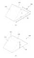
도 1은 본 발명의 실시예에 따른 백라이트 유닛과 이를 구비하는 액정표시장치의 예를 개략적으로 도시한 분해사시도이다.1 is an exploded perspective view schematically showing an example of a backlight unit and a liquid crystal display device having the same according to an embodiment of the present invention.
도 1을 참조하면, 본 발명에 따른 액정표시장치는 상부케이스(11), 액정패널(20) 및 백라이트유닛(100)을 포함하여 구성된다.Referring to FIG. 1, a liquid crystal display device according to the present invention includes an
액정패널(20)은 패널가이드(13)의 패널 지지부에 적층되어 백라이트유닛(100)으로부터 공급되는 광의 투과율을 조절하여 화상을 표시한다. 이를 위해 액정패널(20)은 상부기판(21), 하부기판(22) 및 상부기판(21)과 하부기판(22) 사이에 형성된 액정(미도시)을 포함하여 구성된다.The
상부기판(21)에는 청색, 녹색, 적색의 컬러필터와 블랙매트릭스(Black Matrix : BM) 및 공통전극이 구성된다.In the
하부기판(22)에는 데이터 라인들과 게이트 라인들에 의해 정의되는 셀 영역마다 형성된 박막트랜지스터(Thin Film Transisor)와 박막트랜지스터에 접속된 화소전극이 구성된다. 박막트랜지스터는 게이트 라인으로부터 공급되는 게이트 신호에 응답하여 데이터 라인으로부터 공급되는 데이터 신호를 화소 전극에 공급한다. 여기서, 상부기판(21)에 형성된 공통전극은 하부기판(22)에 형성되도록 할 수 있으며, 제시된 바에 의해 본 발명을 한정하는 것은 아니다. 그리고, 하부기판(22)의 비표시영역에는 데이터 라인들 각각에 접속되는 데이터 패드 영여과 게이트 라인들 각각에 접속되는 게이트 패드 영역이 마련된다.In the
데이터 패드영역에는 데이터 라인들에 화상신호를 공급하기 위한 데이터 집적회로(24)가 실장된 데이터 회로필름(23)이 결합되며, 이때 데이터 회로필름(23)은 복수로 구성될 수 있다. 각 데이터 회로 필름(23)은 테이프 캐리어 패키지(Tape Carrier Package) 또는 칩 온 필름(Chip On Film)으로 구성될 수 있다. 이러한 데이터 회로필름(23)은 데이터 회로기판(미도시)으로부터 데이터 신호 및 화상의 구현을 위해 필요한 신호를 공급받아 각 데이터 라인에 공급한다. 여기서, 데이터 집적회로(24)는 칩 온 글라스(Chip On Glass) 방식에 의해 하부기판(22)에 실장될 수도 있다. 이 경우, 하부기판(22)에 실장된 데이터 집적회로(24)는 데이터 회로필름(23)을 통해 데이터 회로기판으로부터 데이터 신호 및 화상의 구현을 위해 필요한 신호를 공급받을 수 있다.The
게이트 패드영역에는 게이트 라인들에 게이트 신호를 공급하기 위한 게이트 집적회로(26)가 실장된 게이트 회로필름(25)이 결합되며, 이때 게이트 회로필름(25)은 복수로 구성될 수 있다. 이 게이트 회로필름(25)도 테이프 캐리어 패티지 또는 침 온 필름으로 구성되거나, 게이트 집적회로가 하부기판(22)에 실장된 칩 온 글라스 형태로 구성될 수 있다. 이러한 게이트 회로필름(25)은 게이트 회로기판(미도시)으로부터 공급되는 게이트 제어신호를 게이트 집적회로(26)에 공급하고, 게이트 집적회로(26)로부터 공급되는 게이트 신호를 각 게이트 라인에 공급한다.In the gate pad region, a
패널가이드(13)는 도광판(140), 광학시트(110), 반사시트(130)의 가장자리를 감쌈과 아울러, 도광판(140), 광학시트(110) 및 반사시트(130)를 하부케이스(101)에 고정시키는 역할과, 액정패널(13)을 지지하는 역할을 한다. 여기서, 패널가이드(13)의 역할을 하부케이스(101)나 상부케이스(11) 또는 하부케이스(101)와 상부케이스(11)에 부가되는 구조물에 의해 대체되거나 생략될 수 있다.The panel guide 13 covers the edges of the
상부케이스(11)는 액정패널(20)의 전면 비표시 영역을 감싸는 형태로 형성되어, 액정패널(20), 패널가이드(13)를 하부케이스(110)와 함께 고정 및 수납하는 역할을 한다.The
백라이트유닛(100)은 액정패널(20)의 하부에 배치되며, 광을 생성하여 액정패널(20)에 공급한다. 이를 위해 백라이트 유닛(100)은 광원(120), 도광판(140), 광학시트(130)를 포함하여 구성된다. 또한, 백라이트 유닛(100)은 반사시트(130)를 더 포함하여 구성될 수 있다.The
광원(120)은 광원회로기판(121)에 실장되어 전원에 의해 구동되며 광을 생성한다. 이러한 광원(120)은 발광다이오드(Light Emitting Diode : LED), 냉음극관 형광램프(Cold Cathode Flourescent Lamp : CCFL), 외부전극 형광램프(External Electrode fluorescent Lamp : EEFL) 중 어느 하나로 형성될 수 있다. 광원(120)으로부터 방출된 광은 도광판(140) 내부로 입사되고, 도광판(140), 광학시트(110) 및 반사시트(130)에 의해 액정패널(20)에 공급된다. 이러한 광원(120)은 도광판(140)의 적어도 일면과 마주보도록 형성된다.The
특히 본 발명에서는 백라이트 유닛(100)이 에지형으로 구성되는 것이 유리하다. 본 발명의 도광판은 광원(120)에서 방출된 광을 상부 패턴 및 집광시트(112)뿐만 아니라 하부 패턴에 의해 전반사를 유도하고, 이를 통해 광 이용효율 증대(고휘도) 및 모아레 발생을 방지하게 된다. 이러한 이유로 광원(120)이 도광판(140)의 일측면에 구성된 위주로 본 발명을 설명하기로 한다. 하지만, 광원(120)은 도광판(140)의 측면 중 적어도 어느 하나 이상에 구성될 수 있으며, 도광판(140)의 측면과 함께 직하형으로 구성될 수도 있다. 다만, 이 경우 측면에 구성되는 광원(120) 중 모아레 및 휘도에 가장 큰 영향을 미치는 광에 대해 본 발명의 도광판(140)이 적용될 수 있다. 이러한 도광판(140) 및 광원에 대해서는 하기에서 좀 더 상세히 설명하기로 한다.Particularly, in the present invention, it is advantageous that the
광학시트(110)는 도광판(140)을 통해 방출된 광을 집광 또는 확산시켜 액정패널(20)에 전달되도록 한다. 이를 위해 광학시트(130)는 확산시트(111) 또는 집광시트(112)를 하나 이상 포함하여 구성될 수 있다.The
확산시트(111)는 도광판(140)을 통해 방출된 광이 일부 영역에 집중되는 것을 방지하고, 고른 분포로 액정패널(20)에 전달되도록 광을 분산시키는 역할을 한다. 이러한 확산시트(111)는 집광시트(112)와 액정패널(20) 사이, 집광시트(112)와 도광판(140) 사이와 같이 광의 분산이 필요한 곳에 배치될 수 있다. 이를 통해 확산시트(111)는 집광시트(112) 또는 도광판(140)에 의해 집광 또는 집중된 광을 확산시켜 액정패널(20)의 시야각이 좁아지는 것을 방지하고, 광이 고른 분포로 액정패널(20)에 전달될 수 있게 한다. 또한, 확산시트(111)는 필요에 따라 생략될 수 있으며, 이로써 본 발명을 한정하는 것은 아니다. 여기서, 본 발명에서는 액정패널(20)과 집광시트(112) 사이에 확산시트(111)가 배치되는 예를 위주로 상세한 설명을 진행하기로 한다.The
집광시트(112)는 도광판(140)으로부터 방출되는 광을 집광하고, 액정패널(20)에 광이 수직으로 전달될 수 있게 한다. 이를 위해 집광시트(112)는 액정패널(20)을 마주대하는 상면과 도광판(140)을 마주대하는 하면 중 적어도 일면에 집광을 위한 패턴이 형성된다. 특히, 본 발명의 집광시트(112)는 시트패턴이 도광판(140)을 마주대하는 면에 형성되는 리버스 프리즘 시트(Reverse Prism Sheet)로 구성될 수 있다. 그리고 집광시트(112)와 액정패널(20) 사이에는 확산시트(111)가 개재될 수 있으나, 이로써 본 발명을 한정하는 것은 아니다.The
반사시트(130)는 도광판(140)의 하부 또는 측면에 배치되며, 도광판(140)의 측면이나 하부로 방출되는 광을 도광판(140) 내부로 반사시킨다. 이 반사시트(130)는 광원(120)의 배치에 따라 형성위치가 달라질 수 있다. 일례로 에지형 백 라이트 유닛의 경우 도 1에 도시된 바와 같이 도광판(140)의 하부 즉, 도광판(140)을 사이에 두고 액정패널(20)과 마주 대하는 면에 배치될 수 있다. 그리고, 직하형 백라이트 유닛의 경우 도광판(140)의 측면에 구성되거나 필요에 따라 생략될 수 있으며, 제시된 바에 의해서만 한정되지 않고 광원(120)의 배치와 같은 다양한 요인에 의해 변형이 가능하다.The
도광판(140)은 광원(120)으로부터 공급되는 광을 가이드함과 아울러, 광을 집광 및 확산시켜 액정패널(20)로 출사시킨다. 이러한 도광판(140)은 액정패널(20)을 마주대하는 면에 상부패턴(미도시)이 형성되고, 이와 대를 이루는 면에 하부패턴(미도시)이 형성된다. 이러한 상부패턴 및 하부패턴을 통해 도광판(140)은 광원(120)으로부터 공급되는 광을 효율적을 액정패널(20)에 공급하며, 모아레의 발생을 저감 또는 방지하게 된다. 이에 대해서는 하기의 도면을 통해 좀더 상세히 설명하기로 한다.The
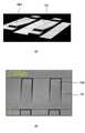
도 2는 본 발명에 따른 도광판의 일례를 도시한 평면사시도이고, 도 3은 상부패턴의 예들을 도시한 예시도이다. 그리고, 도 4는 도 2의 도광판에 대한 배면사시도이다.FIG. 2 is a plan perspective view showing an example of a light guide plate according to the present invention, and FIG. 3 is an exemplary view showing examples of an upper pattern. 4 is a rear perspective view of the light guide plate of Fig. 2. Fig.
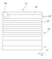
도 2 내지 도 4를 참조하면, 본 발명에 따른 백라이트유닛(100)의 도광판(140)은 베이스(143)의 상면과 하면에 각각 상부패턴(141)과 해부패턴(146)이 형성된다.2 to 4, an
상부패턴(141)은 도광판(140)의 상면에 형성된다. 이 상부패턴(141)은 음각 패턴(V-cut) 패턴(141a)으로 형성될 수 있다. 여기서, 음각 패턴은 입광면으로부터 이에 대를 이루는 면까지 연정되어 도광판(140) 베이스(143)의 상면을 가로지르는 역삼각형 홈(Groove) 형상을 가지도록 형성될 수 있다. 이러한 음각패턴에 의해 도 3의 (a)에 도시된 것과 같이 상부패턴(141a)의 단면 형성이 사다리꼴 형태인 도광판(140a)을 형성할 수 있다. 또는 도 3의 (b)에 도시된 바와 같이 음각패턴을 깊게 하여 상부패턴(141b)의 단면 형상이 삼각형인 도광판(140b)을 형성하는 것도 가능하다.The
아울러, 이러한 상부패턴(141c)은 (c)에 도시된 것과 같이 단면형상이 반구형인 패턴이 연속적으로 형성되도록 하는 것도 가능하며, 패턴의 단면형상은 다양하게 변형이 가능하다.In addition, the
이러한 상부패턴(141)은 도광판(140)의 베이스 내부로 입사된 광이 도광판 내에서 여러번 반사되도록하여 고른 분포로 분산되게 하는 역할을 함과 아울러, 반사를 통해 광이 액정패널(20) 방향으로 집중되도록 하는 역할을 한다. 특히, 상부패턴(141)은 내부에서 반사되는 광 중 상부패턴(141)에 특정 각도로 입사되는 광만 도광판 외부로 출사되도록 함으로써 집광시트(112)에 의한 집광 효과 및 광의 직진성 향상을 통한 휘도가 증가되게 하는 역할을 한다.The
한편, 도 4에서와 같이 도광판(140)의 하면에는 하부패턴(146)이 형성된다. 하부패턴(146)은 베이스(143)의 하면에 음각 또는 양각으로 형성된다. 이 하부패턴(146)은 비대칭 프리즘 형상으로 복수개 형성된다. 이러한 하부패턴(146)은 도광판(140) 내부로 입사된 광의 전반사 효과를 향상시켜 광의 이용효율을 증가시키고 휘도를 향상시킨다. 또한, 하부패턴(146)은 도광판(140) 내부의 광 분포를 균일, 균등하게 하는 역할을 하며, 액정패널(20)의 블랙매트릭스, 광학시트(110)의 패턴, 도광판(140) 상부패턴(141) 간의 공간주파수 차이로 발생하는 모아레(Moire)를 저감 또는 방지하는 역할을 한다. 이를 위해 하부패턴(146)은 패턴간의 간격, 크기, 패턴의 형성각이 조절되어 형성된다.4, a
도 5는 하부패턴의 형태를 도시한 예시도이고, 도 6은 하부패턴이 양각 또는 음각형태로 도광판 베이스에 적용된 예를 도시한 사시도이다.FIG. 5 is an exemplary view showing the shape of the lower pattern, and FIG. 6 is a perspective view showing an example in which the lower pattern is applied to the light guide plate base in the form of a relief or a negative angle.
도 5 및 도 6을 참조하면, 하부패턴(146 : 146a, 146b)와 같이 비대칭 입체로 형성된다. 특히 광을 반사시키기 위한 한 면 이상의 경사면(147a)이 형성된다. 또한 이 경사면(147a)과 마주대하는 다른 부경사면(147b)이 형성될 수 있으며, 이때 대를 이루는 경사면(147a)과 부경사면(147b)은 평행하지 않게 형성된다. 부경사면(147b)은 밑변(148)에 대해 직각으로 형성될 수 있으나, 이로써 본 발명을 한정하는 것은 아니다. 즉, 이 하부패턴(146)은 프리즘과 유사한 형태로 형성될 수 있으며, 경사면(147a)과 부경사면(147b)이 전반사를 위해 비대칭으로 형성된다.Referring to FIGS. 5 and 6, the lower pattern 146 (146a, 146b) is formed as an asymmetric solid. An
또한, 경사면(147a)과 부경사면(147b) 사이에는 경사면(147a)과 다른 경사도를 가지는 랜드부(147c)가 형성될 수 있다.A
이러한 하부패턴(146)은 도광판(140) 하부면(144)에 음각되어 형성되는 음각하부패턴(146c)이나, 도드라지게 형성되는 양각하부패턴(146d)으로 복수개 형성될 수 있다.The
여기서, 하부패턴(146)이 음각되어 형성되는 음각하부패턴(146c)은 경사면(147a)이 광이 입사되는 베이스면인 입광면(149)을 향하도록 형성되고, 양각하부패턴(146d)의 경우 부경사면(147b)이 입광면(149)을 향하도록 형성된다. 이를 통해, 입광면(149)을 통해 입사되어, 도광판(140) 베이스(143) 내부를 진행하는 광이 경사면(147a)에 전반사되어 도광판(140)으로 출사된다.Here, the concave
아울러, 본 발명에서는 하부패턴(146)의 길이(L)과 폭(W)이 도 5에 도시된 바와 같이 정의된다. 구체적으로 하부패턴(146)을 측면에서 봤을 때 경사면(147a)와 부경사면(147b)에 의해 형성되는 삼각형(또는 사다리꼴)의 밑변(148)(즉, 도광판 하부면)의 길이(L)가 하부패턴(146) 각각의 길이(L)로 정의 되고, 이 길이(L) 방향과 수직 방향의 경사면(147a) 또는 부경사면(147b) 폭이 하부패턴(146)의 폭(w)으로 정의된다.In addition, in the present invention, the length L and the width W of the
이에 대한 설명이 도 7 및 도 8에 도시되어 있다.A description thereof is shown in Figs. 7 and 8. Fig.
도 7은 음각 및 양각 하부패턴의 경사면 형성 각도를 설명하기 위한 예시도이고, 도 8은 양각 하부패턴에 의한 전반사 효과를 설명하기 위한 예시도이다.FIG. 7 is an exemplary view for explaining an inclined plane forming angle of the negative embossed pattern and the embossed bottom pattern, and FIG. 8 is an exemplary view for explaining the total reflection effect by the embossed bottom pattern.
도 7 및 도 8을 참조하면, 본 발명의 하부패턴(146c, 146d)은 도광판(140)의 베이스(143) 내부를 진행하는 광(LI)을 도광판 전면(또는 전면의 상부패턴(141))을 통해 출사시키는 역할을 한다. 특히, 하부패턴(146c, 146d)은 도 8에 도시된 바와 같이 광(LI)이 특정각으로 출사되도록 하는 역할을 한다. 여기서 도 8에는 양각하부패턴(146d)이 대표로 도시되어 있으나, 음각하부패턴(146c)에 의한 작용도 이와 동일하다.7 and 8, the
구체적으로 도광판(140) 전면을 통해 출사되는 광은 도광판(140)의 전면에 대해 일정한 출사각(θL)을 유지할 때, 집광시트(112)에 의한 집광 효율이 증가하여 휘도 증가효과를 기대할 수 있게 된다. 이때, 출사각(θL)은 도광판 전면에 대해 10도 내지 30내 이내의 범위로 출사되는 것이 바람직하며, 이 범위 내의 각도로 출사된 광이 집광시트(112)에 의해 효율적으로 집광된다.Specifically, when light emitted through the entire surface of the
아울러, 출사각(θL) 범위 이외의 각도로 출사되는 광(LI)은 도광판(140) 상부패턴(141) 또는 집광시트(112)에 의해 순환 및 재사용되게 된다. 즉, 본 발명의 도광판(140)은 출광되는 광(LI)이 상부패턴(141) 및 집광시트(112)에 의해 집광이 유리한 방향 즉, 전반사 효과가 최적이 될 수 있는 방향으로 출광시킨다. 또한, 집광시트(112) 또는 상부패턴(141)과 도광판(140) 하부면(144) 사이에 순환 소모되어 낭비될 수 있는 광의 이용효율을 향상시키게 되어 동일한 광원을 이용하더라도 집광효율 및 휘도를 향상시킬 수 있게 된다.The light LI emitted at an angle other than the outgoing angle? L is circulated and reused by the
이러한 효과의 획득을 위해 도 7에 도시된 바와 같이 하부패턴(146c, 146d)은 전술한 바와 같이 경사면(147a)을 가지는 형태로 음각 또는 양각되어 도광판(140) 하부면(144)에 형성된다. 그리고 도 8에 도시된 바와 같이 경사면(147a)에 의한 전반사에 의해 입사된 광(LI) 또는 도광판(140) 내부를 이동하는 광(LI)의 경로를 변경시켜, 광(LI)이 특정각으로 출사될 수 있게 한다. 이를 위해 음각하부패턴(146c) 또는 양각하부패턴(146d)의 경사면(147a)은 미리 정해진 경사도를 가지도록 경사도가 결정된다.As shown in FIG. 7, the
구체적으로 도 7에 도시된 바와 같이 경사면(147a)와 도광판(140) 하부면(144)이 이루는 경사면각(θ1)은 부경사면(147b)와 도광판(140) 하부면(144)이 이루는 부경사면각(θ2)에 비해 작게 형성된다(θ1<θ2). 더욱 구체적으로 경사면각(θ1)은 전반사 효과 및 출사각(θL)을 10도 이상 30 도 이하의 특정각으로 출사되기 유리하도록 5도이상 10도 이하 범위내의 각도일 수 있다. 아울러, 경사면(147a)과 부경사면(147b) 사이의 사잇각(θ3)는 50도 이상 170도 이하의 각일 수 있다.7, the slope angle? 1 formed by the
물론, 경사면각(θ1), 부경사면각(θ2), 사잇각(θ3)이 전술한 각도 범위를 벗어나도록 하여 형성될 수도 있으나, 이 경우 전반사 효과가 저하되고 휘도 향상효과가 저하되어 하부패턴(146)에 의한 효과 향상을 기대하기 곤란해진다.Of course, the inclined angle? 1, the inclined angle? 2 and the inclined angle? 3 may be formed to deviate from the angular range described above. In this case, the total reflection effect is lowered, It is difficult to expect an improvement in the effect of the above.
또한, 전술한 바와 같이 하부패턴(146)의 경사면(147a)은 도광판(140)의 입광면(149)을 통해 입사되는 광의 반사를 위한 형태로 배치된다. 구체적으로, 양각하부패턴(146d)의 경우 부경사면(147b)이 입광면(149)을 향하고, 경사면(147a)은 입광면(149)과 마주보는 도광판 측면인 반입광면(149b)을 향하도록 하여 도광판(140) 하부면(144)에 형성된다.In addition, as described above, the
반대로 음각하부패턴(146c)은 양각하부패턴(147d)과 반대되는 형상으로 형성된다. 구체적으로 경사면(147a)이 입광면(149)을 향하고, 부경사면(147b)이 반입광면(149b)를 향하도록 하여 도광판(140) 하부면(144)에 형성된다.Conversely, the engraved
도 9는 백라이트의 유닛 구조를 설명하기 위한 예시도이고, 도 10은 양각하부패턴의 형성예를 설명하기 위한 예시도이다.9 is an exemplary view for explaining a unit structure of a backlight, and Fig. 10 is an exemplary view for explaining an example of forming an embossed lower pattern.
도 9 및 도 10을 참조하면, (a)에서와 같이 백라이트 유닛(100)은 광학시트(110), 도광판(140) 및 반사시트(130)가 순차적으로 적층되며, 도광판(140)의 일 측면인 입광면(149)에 광원(120)이 배치된다.9 and 10, the
이러한 백라이트 유닛(100)은 반사시트(130) 상에 도광판(140)이 위치하고, 도광판(140) 상에 광학시트(110)가 배치된다. 특히, 도광판(140)에 형성된 하부패턴(146)은 도 8에 도시된 바와 같이 종축을 따라 톱니형태가 되도록 도광판(140)의 하부면(144)에 형성된다. 그리고 상부패턴(141)은 종축과 나란하게 도광판(140)의 상면에 형성된다.In this
도광판(140)의 상부에는 광학시트(110)가 적층되며, 광학시트(110)는 도광판(140) 상부패턴(141) 상에 적층되는 집광시트(112)와 집광시트(112) 상에 형성되는 확산시트(111)로 구성된다. 집광시트(112)는 도시된 바와 같이 시트패턴(112a)이 도광판(140)의 상부패턴(141)과 마주보도록 도광판(140) 상에 적층된다. 여기서, 시트패턴(112a)은 도광판(140) 상부패턴(141)과 같이 일방향으로 긴 프리즘 형상(또는 렌티큘러 렌즈)으로 형성된다. 그리고 집광시트(112)는 시트패턴(112a)이 도광판(140) 상부패턴(141)과 교차하도록 도광판(140) 상에 배치된다.The
도 9의 (b)에는 광원(120)과 상부패턴(141) 및 하부패턴(146)의 관계를 보여주기 위한 도면이 도시되어 있다. (b)에서와 같이 상부패턴(141)은 종축(Vx)에 나란하게 일방향으로 형성된다. 아울러, 하부패턴(146)도 종축(Vx)을 따라 배열되며, 입광면(149)에서 멀어질수록 패턴간격(P)이 좁아지고, 패턴폭(W)은 넓어지게 형성될 수 있다. 이를 통해 광원(120)에서 먼 부분 즉, 광의 밀도가 상대적으로 적은 부분에서 하부패턴(146)에 의한 광의 반사율을 높임으로써 도광판(140) 전체의 광 분포가 균일해지게 한다.9B is a view showing the relationship between the
도 10은 양각하부패턴(146d)의 형성예가 도시되어 있다. 도 9 및 도 10에서와 같이 양각하부패턴(146d)은 도광판 하부면(144)에 대해 돌출된 형태로 형성된다. 이러한 하부패턴(146)의 사이 공간은 평평한 면 즉, 평부(151, Flat Surface)가 형성된다. 도 9의 (b)에서는 종축(Vx)에 나란한 방향으로 평부(151)가 형성된 것으로 도시되어 있으나, 횡축(Hx)와 나란한 방향의 하부패턴(146) 사이의 공간도 평부(151)로 형성된다.Fig. 10 shows an example of the formation of the embossed pattern 146d. 9 and 10, the embossed
본 발명의 도광판(140)은 하부패턴(146) 사이의 공간을 평부(151)로 형성함으로써, 입사된 광이 도광판(140)의 다른 부분으로 균일하게 전파될 수 있게 한다. 구체적으로, 도광판(140)에 입사된 광 중 평부(151)로 진행하는 광은 평부(151)에 의해 도광판(140) 내부로 반사되고, 상부패턴(141)에 의해 도광판(140) 내부에서 확산된다. 그리고, 이와 같이 평부(151)에 의해 반사된 광 일부는 하부패턴(146)과 상부패턴(141)에 의해 도광판(140) 상면으로 출사되고, 나머지 광은 내부에서 재반사 및 이용되어 광의 균일도와 이용효율을 증대에 기여하게 된다.The
도 11은 하부패턴의 형성을 설명하기 위한 예시도이다.11 is an exemplary view for explaining formation of a lower pattern.
본 발명의 도광판(140)은 전술한 바와 같이 하부패턴(146)에 의해 광의 이용효율을 증대시켜 휘도를 향상시키는 역할을 한다. 또한 이와 더불어 본 발명의 도광판(140)은 도광판(140) 전면에 대해 광분포를 균일하게 하고, 모아레(Moire) 발생을 방지 또는 저감한다.As described above, the
이를 위해 하부패턴(146)은 길이, 폭, 하부패턴(146)간 간격, 형성각을 달리하여 도광판(140)에 형성될 수 있다.For this, the
에지형 백라이트 유닛(100)은 일반적으로 도광판(140)의 4측면 중 일측면인 입광면(149)에 대면하여 광원(120)이 구성된다. 때문에 광원(120)과 인접한 입광면(149) 부근의 도광판(140)은 광의 밀도가 높아 휘도가 높아지고, 이와 상대적으로 거리가 먼 반입광면(149b)은 광의 밀도가 낮아 휘도가 저하되는 현상이 발생한다. 즉, 반입광면(149b)에 가까울수록 광의 밀도가 저하되어 어두워지는 현상이 발생하고, 이로 인해 화상 구현시 품위가 저하되는 원인이 된다.The edge
이러한 광의 밀도 차를 해소하기 위해 본 발명의 하부패턴(146)은 입광면(149)에 근접한 부분과 반입광면(149b)에 근접한 부분의 패턴길이(L), 패턴폭(W), 패턴간 간격(P), 경사면(147a)의 경사면각(θ1), 깊이(D) 중 적어도 어느 하나를 달리하여 형성될 수 있다. 여기서 깊이(D)는 도광판(140) 하부면(144)으로부터 경사면(147a)과 부경사면(147b)가 마주대하는 모서리까지의 최단거리 또는 경사면(147a)과 부경사면(147b) 사이에 형성되는 랜드부(147c)까지의 거리를 의미한다(도 3 참조).The
구체적으로 광의 밀도가 상대적으로 큰 입광면(149)의 경사면(147a) 면적에 비해 광의 밀도가 상대적으로 작은 반입광면(149b)의 경사면(147a) 면적을 넓게하여 도광판(140) 전면으로 반사되는 광량을 조절함으로써 도광판(140)의 광 분포를 조절하는 것이 가능하다.The area of the
이를 위해 복수의 하부패턴(146) 중 입광면(149)에 인접한 하부패턴(146)의 패턴폭(W)을 반입광면(149b)에 인접한 하부패턴(146)의 패턴폭(W)에 비해 좁게 형성하거나, 입광면(149)에 인접한 하부패턴(146)의 패턴길이(L)을 반입광면(146b)에 인접한 하부패턴(146)의 패턴길이(L)에 비해 짧게 형성할 수 있다. 또는 복수의 하부패턴(146) 중 입광면(149)에 인접한 패턴 간의 간격(P)을 반입광면(149b)에 인접한 패턴간의 간격(P)에 비해 넓게 형성할 수 있다.The pattern width W of the
이를 통해 도광판(140) 단위 면적당 하부패턴(146)의 반사면적을 달리함으로써 도광판(140)에 의해 출사되는 광의 분포를 균일하게 조절하는 것이 가능해진다. 더욱이 반입광면(149b) 또는 입광면(149)에 인접한 하부패턴(146)이라 해도, 중앙과 양측 가장자리에 인접한 정도에 따라 길이(L), 폭(W), 패턴간 간격(P)은 상이해질 수 있다.It is possible to uniformly control the distribution of the light emitted by the
또한, 빛의 집중 및 분산을 조절하여 광분포를 조절하는 것이 가능하면, 이를 위해 경사면각(θ1) 또는 깊이(D)를 가변하여 형성하는 것이 가능하다.In addition, if it is possible to adjust the light distribution by adjusting the concentration and dispersion of light, it is possible to vary the angle of inclination? 1 or the depth D for this purpose.
좀 더 구체적으로 설명하면, 도 11에 도시된 바와 같이 길이(L), 폭(W), 패턴간격(P)이 동일하게 하여 도광판(140)에 하부패턴(146)을 형성할 수 있다(영역A).11, the
또는 도 11의 영역B, 영역C, 영역D와 같이 길이(L), 폭(W) 및 간격(P) 중 어느 하나를 가변하여 하부패턴(146)을 형성할 수도 있다.Alternatively, the
구체적으로 영역 A(A)는 패턴간격(P), 폭(W), 길이(L)를 모두 균일하게 하여 하부패턴(146)이 형성된 예이다. 그리고, 영역B(B)는 폭(W) 및 간격(P)은 일정하게 하고 입광면(149)과의 거리가 증가할수록 패턴의 길이(L)가 길게 형성된 예가 도시되어 있다.Specifically, the area A (A) is an example in which the
또한, 영역C(C)는 패턴의 길이(L)와 패턴간격(P)은 일정하게 하고, 입광면(149)와 거리에 따라 폭(W)을 달리하여 형성한 예가 도시되어 있다. 마지막으로 영역(D)는 패턴의 길이(L)와 폭(W)은 동일하게 하고 입광면(149)과의 거리가 증가할수록 패턴간격(P)을 감소시켜 하부패턴(146)을 형성한 예가 도시되어 있다.The area C (C) shows an example in which the length L of the pattern and the pattern interval P are made constant and the width W varies according to the distance from the
이 영역B, 영역C, 영역D는 입광면(149)에 인접한 도광판(140)의 단위면적당 하부패턴(146)에 의한 반사면, 즉, 경사면(147a)의 면적이 반입광면(149b)의 단위면적당 경사면(147a)의 넓이가 상대적으로 적게 된다. 이를 통해 광 밀도 높은 부분에서는 적게 반사하고, 광 밀도가 낮은 부분에서는 광을 많이 반사하여 출광시킴으로써 도광판(140) 전면에 광이 고른 분포로 출사될 수 있게 조절하게 된다.The area B, the area C and the area D are reflection surfaces of the
한편, 하부패턴(146)은 길이(L), 폭(W) 및 간격(P)의 변경을 복합적으로 적용하여 형성될 수 있다.On the other hand, the
구체적으로 도광판(140)을 입광면(149)에 인접한 제1영역과 반입광면(149b)에 인접한 제2영역과 같이 도광판(140)의 입광면(149)과의 거리 또는 광 밀도에 따라 복수의 영역으로 구분하고, 영역에 따라 가변되는 요소를 달리하여 하부패턴(146)을 형성할 수 있다.Specifically, the
일례로 도 11에서 점선으로 구분된 2영역인 제1영역(SA)와 제2영역(SB)은 길이(L), 폭(W), 간격(P), 깊이(D) 중 가변되는 요소를 달리하여 하부패턴(146)이 형성될 수 있다.For example, the first area SA and the second area SB, which are two areas divided by a dotted line in FIG. 11, are elements that vary in length L, width W, interval P, and depth D The
일례로 제1영역(SA)의 하부패턴(146)은 패턴간 간격(P)은 균일하게 하고 하부패턴(146)의 길이(L) 또는 폭(W)을 단계적(또는 선형적)으로 변경하여 형성하고, 제2영역(SB)은 패턴 길이(L) 또는 폭(W)은 균등하게 하고 길이(L), 폭(W), 간격(P)을 균등하게 하되 제1영역과 다른 값을 가지도록 하여 하부패턴(146)을 형성할 수 있다. 아울러, 이와 같이 도광판(140)의 하부면(144)을 복수의 영역으로 구분하는 경우 각 영역에 따라 가변되는 요소는 사용자에 의해 선택될 수 있는 사항으로 제시된 바에 의해 본 발명을 한정하는 것은 아니다.The
도 12는 모아레 방지를 위한 하부패턴의 형성을 설명하기 위한 예시도이고, 도 13은 도광판 패턴 주기에 따른 모아레 발생 및 미발생 피치를 도시한 예시도이다.FIG. 12 is an exemplary view for explaining the formation of a lower pattern for preventing moire, and FIG. 13 is an exemplary view showing a moire occurrence and a non-generated pitch according to a light guide plate pattern period.
도 12 및 도 13을 참조하면, 본 발명의 도광판(140)은 모아레(Moire)의 발생을 방지 또는 저감할 수 있다.12 and 13, the
모아레는 액정패널(20)에 형성되는 블랙매트릭스(BM), 광학시트(110)의 패턴과 도광판의 패턴에 의해 광의 집중과 분산이 발생하여 화면에 굵은 줄무늬가 발생하는 형상의 의미한다. 이는 패턴, 블랙매트릭스의 공간 주파수의 차에 의해 발생하는 현상으로 화상 구현의 품위를 저하시키는 원인이 된다.The moiré refers to a shape in which light is concentrated and dispersed by a black matrix BM formed on the
특히, 모아레는 액정패널(20)의 블랙매트릭스(BM)와 다른 광학구성 간의 공간주파수 차이로 인해 발생하는 경우가 많다. 때문에 블랙매트릭스(BM)로 인한 패널주기와 도광판(140)에 의한 주기를 조절하여 이러한 모아레의 발생을 방지할 수 있다.In particular, the moire is often generated due to the spatial frequency difference between the black matrix BM of the
이러한 블랙매트릭스(BM)와의 사이에 발생하는 모아레는 도 13에 도시된 바와 같이 하부패턴(140) 간의 간격(P)에 따라 특정 거리 예를들어 62.13㎛, 91.38㎛, 182.38㎛에서 사용자에 인식 가능할 정도로 발생함을 알 수 있다.The moiré generated between the black matrix BM and the black matrix BM can be recognized by the user at a specific distance, for example, 62.13 μm, 91.38 μm, and 182.38 μm according to the interval P between the
때문에, 모아레의 발생을 방지하기 위해서 도광판(140)에 형성되는 하부패턴(146) 간의 간격(P)을 모아레가 발생하지 않는 간격으로 형성함으로써 모아레의 발생을 방지 또는 저감할 수 있다.Therefore, in order to prevent occurrence of moire, the interval P between the
모아레는 액정표시장치의 광학구성 예를 들어, 액정패널(20), 광학시트(110), 도광판(140) 상호 간의 공간 주파수 차이로 인해 발생한다. 특히, 이러한 광학구성 중 액정패널(20)의 블랙매트릭스(BM)와 도광판(140) 하부패턴(146) 간에 발생하는 모아레가 화상의 품질을 저하시키는 주요원인이 된다.The moiré occurs due to the spatial frequency difference between the
이를 해소하기 위해 하부패턴(146)의 패턴간격(P)을 조정함으로써 모아레 발생을 방지 또는 저감할 수 있다.In order to solve this problem, it is possible to prevent or reduce the generation of moiré by adjusting the pattern interval P of the
도 13에서 가로축은 하부패턴(146)의 패턴간격(P)을 나타낸 것이고, 세로 축은 모아레의 시인성을 나타낸 것이다. 도 13은 블랙매트릭스(BM) 간격은 일정하게 유지한 상태에서 해부패턴(146)의 패턴간격(P)을 가변할 때 모아레의 발생을 나타낸 그래프이다. 도 13에서 블랙매트릭스의 간격이 183㎛로 고정되어 있고, 패턴간격(P)을 49㎛로부터 183㎛로 가변시켰을 때의 모아레 발생이 도시되어 있으며, 62㎛ 부근, 91.5㎛부근, 182㎛부근의 패턴간격(P)을 가질 때 모아레가 발생함을 확인할 수 있다.13, the abscissa represents the pattern interval P of the
여기서, 도 13은 블랙매트릭의 행간 간격(종축 방향 BM간 간격)을 183㎛로 고정하고, 패턴간격(P)도 종축간 간격을 가변하여 실험한 데이터를 그래프로 도시한 것이지만, 블랙매트릭스의 열간 간격(횡축 방향 BM간격) 및 횡축간 패턴간격(P)에도 동일하게 적용된다.13 is a graph showing experimental data in which the inter-line spacing of black matrices (interval between the longitudinal axis BM) is fixed at 183 m and the interval between the vertical axes of the pattern intervals P is also varied. However, The same applies to the interval (in the direction of the transverse axis BM) and the pattern pitch P in the direction of the transverse axis.
이를 구체화하면, 블랙매트릭스의 간격(또는 주기, 또는 BM간 거리)에 대해 약 35%이상 47%이하, 55%이상 97%이하의 값을 하부패턴(146)의 패턴간격(P)으로 적용하는 경우 모아레 발생이 최소화됨을 확인할 수 있다. 즉 도 13에서 블랙매트릭스의 간격이 183㎛일 때 패턴간격(P)을 64.05㎛이상 86.01㎛이하, 100.65㎛이상 177.51㎛이하의 값으로 하여 형성하는 경우 모아레의 발생을 방지할 수 있게 된다.A value of about 35% or more and 47% or less and 55% or more and 97% or less with respect to the interval (or period or BM distance) of the black matrix is applied as the pattern interval P of the
또는 도 12에서와 같이 하부패턴(146)의 형성시 틸팅(Tilting)에 의해 모아레 발생을 방지하는 것이 가능하다. 구체적으로 하부패턴(146)의 형성시 하부패턴(146)이 종축(VX) 또는 횡축(HX) 중 적어도 어느 한 축에 대해 일정 각도로 비스듬하게 형성한다. 이를 통해 패널주기와 도광판 패턴 주기의 겹침을 방지하여 모아레를 방지할 수 있다. 여기서, 횡축(HX)은 입광면(149)과 평행한 방향을 의미하고, 종축(Vx)은 입광면(149)에 대해 수직인 방향을 의미한다.Or it is possible to prevent moiré generation by tilting when forming the
이에 대해 좀더 구체적으로 설명하면, 하나의 열 또는 하나의 행을 이루는 하부패턴(146)의 형성시 각 하부패턴(146)의 동일한 위치(예를 들어 경사면(147a)의 중앙)을 잇는 가상의 정렬선(S)이 종축(VX) 또는 횡축(HX)과 나란해지지 않도록, 틸팅된 하부패턴(146)이 형성된다. 이때 틸팅각은 어느 한 축에 대해 2° 이상 10°이하의 값일 수 있다.More specifically, when forming the
도 12에 도시된 바와 같이 각 하부패턴 열(146r)이 종축(VX)에 대해 경사지게 형성될 수 있다. 이 경우 각 하부패턴열(146r)의 정렬선 종축(VX)에 대해 한 방향으로 나란하게 틸팅되어 형성되거나, 부채살 형상으로 서로 다른 틸팅각을 가지도록 하여 형성될 수 있다.Each
도 14 내지 도 19는 본 발명에 따른 백라이트 유닛의 제조방법 중 도광판의 패턴 형성 과정을 도시한 예시도들이다.FIGS. 14 to 19 are illustrations showing a pattern formation process of a light guide plate in a method of manufacturing a backlight unit according to the present invention.
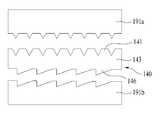
도 14 내지 도 19를 참조하면, 본 발명에 따른 백라이트 유닛의 제조방법은 광원준비단계(S10), 베이스준비 단계(S20), 상부패턴형성 단계(S30) 및 하부패턴형성 단계(S40)을 포함하여 구성된다.14 to 19, a method of manufacturing a backlight unit according to the present invention includes a light source preparation step S10, a base preparation step S20, an upper pattern formation step S30, and a lower pattern formation step S40 .
광원준비단계(S10)는 엘이디(LED)와 같은 발광소자를 이용하여 광원(120)이 마련되는 단계이다.In the light source preparation step S10, the
베이스준비 단계(S20)는 광원준비단계(S10)에서 마련된 광원(120)로부터 발생된 광을 액정패널(20)로 가이드하는 도광판(140)의 모재인 베이스(143)를 준비하는 단계이다.The base preparation step S20 is a step of preparing the base 143 which is the base material of the
상부패턴형성단계(S30)는 베이스준비 단계(S20)에서 준비된 베이스(143)에 도 15와 같이 상부패턴(141)을 형성하는 단계이다. 이 상부패턴형성 단계(S30)에서 베이스(143)의 표면을 절삭팁(189)에 의해 절삭하여 홈(groove)을 형성함으로서 상부패턴이 형성되게 된다.The upper pattern formation step S30 is a step of forming the
하부패턴형성 단계(S40)에서 베이스(143)의 하면에 하부패턴(146)이 형성되는 단계이다. 이 하부패턴형성 단계(S40)에서는 베이스(143) 하부면(144)에 음각하부패턴(146c) 또는 양각하부패턴(146d)을 형성하는 단계이다.And the
이 하부패턴형성 단계(S40)는 형성되는 하부패턴(146)이 음각하부패턴(146c)인지 양각하부패턴(146d)인지에 따라 제조 방법이 달라진다.In the lower pattern forming step S40, the manufacturing method is changed depending on whether the
구체적으로 음각하부패턴(146c)을 형성하는 경우 미리 지정된 위치를 절삭팁(189)에 의해 절삭 가공하여 경사면(147a)와 부경사면(147b)를 형성함으로써 하부패턴(146)을 형성할 수 있다. 즉, 하부패턴(146) 형성 위치만을 부분적으로 절삭하여 도 4에 도시된 것과 같은 음각하부패턴(146c)을 도광판(140) 하부면(143)에 형성할 수 있다.Concretely, when the engraved
반면, 양각하부패턴(146d)의 경우 도 16 내지 도 18에 도시된 절차에 의해 형성될 수 있다. 구체적으로 하부패턴형성 단계(S40)는 양각하부패턴(146d)을 형성하기 위한 하부절삭단계와 평부형성단계를 포함하여 구성될 수 있다.On the other hand, in the case of the
하부절삭단계는 도 16에서와 같이 절삭팁(189)을 이용하여 도광판(140) 하부면(144)에 홈을 형성하고 이를 통해 일방향으로 경사면(147a)과 부경사면(147b)이 이어진 선패턴(247)을 형성하는 단계이다.The lower cutting step may be performed by forming a groove on the
평부형성단계는 도 17에 도시된 바와 같이 선패턴(247)으로 형성된 패턴을 각각의 분리된 하부패턴(146d)으로 형성하기 위해 선패턴(247)을 분리하는 단계이다. 구체적으로 평부형성단계는 선패턴(247)이 형성된 도광판(140) 하부면(144)을 선패턴(247)과 교차하는 방향 또는 나란한 방향으로 절삭팁(189)에 의한 절삭을 수행하여 평부(151)를 형성하게 된다. 이를 통해 절삭팁(189)이 이동한 방향에 따라 평부(151)가 형성되고, 평부(151)에 의해 선패턴(247) 형태로 이어진 패턴이 각각의 하부패턴(146)으로 분리되어 형성되게 된다.The flattening step is a step of separating the
특히, 하부패턴형성 단계(S40)는 도 18에 도시된 바와 같이 하부패턴(146)이 도광판(140)의 종축(Hx) 또는 횡축(Vx)에 대해 미리 정해진 각도로 비스듬하게 형성되는 틸팅 과정이 포함된다. 여기서, 도 18에는 절삭팁(189)에 의해 종축(Hx) 방향으로 틸팅이 이루어진 예가 도시되어 있으나, 이로써 본 발명을 한정하는 것은 아니며, 횡축(Vx) 방향에 대해서도 동일한 방법에 의해 하부패턴(146)을 틸팅하는 것이 가능하다.Particularly, the lower pattern forming step S40 is a tilting process in which the
한편, 이와 같은 절삭 공정을 이용하는 방법 외에 압출(또는 압착)에 의해 도광판을 형성하는 것이 가능하다. 이러한 압착에 의해 도광판 제조 방법의 예가 도 19에 도시되어 있다. 도 19를 참조하면, 베이스 준비 단계(S20)에서 베이스(143)가 준비되면, 전술한 도 16 내지 도 18과 같은 절삭 방법에 의해 상부 금형(191a)와 하부금형(191b)을 준비하는 금형준비단계가 수행된다. 이 금형준비단계에서 상부금형(191a)와 하부금형(191b)에는 각각 상부패턴(141)과 하부패턴(146)에 대응되는 형상이 절삭과 같은 선공정에 의해 형성된다.On the other hand, it is possible to form a light guide plate by extrusion (or pressing) in addition to a method using such a cutting process. An example of a method for manufacturing a light guide plate by such pressing is shown in Fig. 19, when the
금형준비단계에서 상부금형(191a)와 하부금형(191b)가 준비되면, 이 상부금형(191a)와 하부금형(191b) 사이에 베이스(143)를 개재하고 압착하는 압착단계가 수행된다. 상부금형(191a)과 하부금형(191b)에 의해 베이스(143)를 압착하면 금형(191 : 191a, 191b)에 형성된 형상에 의해 베이스(143)가 압착되어 상부패턴(141)과 하부패턴(146)이 형성되게 된다.When the
이와 같이 본 발명의 도광판(140)은 절삭 또는 압착에 의해 용이하게 형성이 가능하다.As described above, the
이상에서 본 발명의 기술적 사상을 예시하기 위해 구체적인 실시 예로 도시하고 설명하였으나, 본 발명은 상기와 같이 구체적인 실시 예와 동일한 구성 및 작용에만 국한되지 않고, 여러가지 변형이 본 발명의 범위를 벗어나지 않는 한도 내에서 실시될 수 있다. 따라서, 그와 같은 변형도 본 발명의 범위에 속하는 것으로 간주해야 하며, 본 발명의 범위는 후술하는 특허청구범위에 의해 결정되어야 한다.While the present invention has been particularly shown and described with reference to exemplary embodiments thereof, it is to be understood that the invention is not limited to the disclosed exemplary embodiments, . ≪ / RTI > Accordingly, such modifications are deemed to be within the scope of the present invention, and the scope of the present invention should be determined by the following claims.
11 : 상부케이스13 : 패널가이드
20 : 액정패널21 : 상부기판
22 : 하부기판23 : 데이터 회로필름
24 : 데이터 집적회로25 : 게이트 회로필름
26 : 게이트 집적회로100 : 백라이트유닛
101 : 하부케이스110 : 광학시트
111 : 확산시트112 : 집광시트
120 : 광원121 : 광원회로기판
130 : 반사시트140 : 도광판
141 : 상부패턴143 : 베이스
143l, 149 : 입광면146 : 하부패턴
147a : 경사면147b : 부경사면
147c : 랜드부149b : 반입광면11: upper case 13: panel guide
20: liquid crystal panel 21: upper substrate
22: lower substrate 23: data circuit film
24: data accumulation circuit 25: gate circuit film
26: Gate integrated circuit 100: Backlight unit
101: Lower case 110: Optical sheet
111: diffusion sheet 112: condensing sheet
120: light source 121: light source circuit board
130: reflective sheet 140: light guide plate
141: upper pattern 143: base
143l, 149: incoming face 146: bottom pattern
147a:
147c:
Claims (26)
Translated fromKorean상기 광학시트를 사이에 두고 상기 출사면과 마주대하도록 상기 백라이트 유닛 상에 배치되고, 블랙매트릭스가 형성되는 기판을 가지는 액정패널;을 포함하여 구성되고,
상기 하부패턴간 간격은
상기 블랙매트릭스의 간격에 대해 35%이상 47%이하 또는 55%이상 97%이하의 값이고
상기 하부패턴의 동일한 위치를 잇는 가상의 정렬선은 입광면에 평행한 횡축 또는 입광면에 수직인 종축에 대해 2°이상 10°이하로 틸팅되는 것을 특징으로 하는 백 라이트 유닛을 포함하는 액정표시장치.A light source that generates light; a lower pattern that guides light through an incident surface facing the light source and emits the light through an exit surface; and a plurality of lower patterns formed in a prism shape by an inclined surface and a sub- A backlight unit including a light guide plate and at least one optical sheet stacked on the exit surface; And
And a liquid crystal panel disposed on the backlight unit so as to face the emission surface with the optical sheet interposed therebetween, the substrate having a black matrix formed thereon,
The interval between the lower patterns is
Is not less than 35% and not more than 47% or not less than 55% and not more than 97% with respect to the interval of the black matrix
Wherein the imaginary alignment line connecting the same position of the lower pattern is tilted by at least 2 DEG and not more than 10 DEG with respect to the horizontal axis parallel to the light incidence surface or the vertical axis perpendicular to the light incidence surface. .
상기 하부패턴은
상기 하부면에 패턴이 오목하게 형성되는 음각하부패턴 또는
상기 하부면에 패턴이 볼록하게 돌출되어 형성되는 양각하부패턴인 것을 특징으로 하는 백 라이트 유닛을 포함하는 액정표시장치.11. The method of claim 10,
The lower pattern
An engraved lower pattern in which the pattern is concave on the lower face or
And wherein the backlight unit is an embossed lower pattern formed by protruding a pattern convexly on the lower surface.
상기 경사면과 상기 하부면이 이루는 각인 경사면각은 상기 하부면과 상기 부경사면이 이루는 각인 부경사면각에 비해 작은 각도인 것을 특징으로 하는 백 라이트 유닛을 포함하는 액정표시장치.11. The method of claim 10,
Wherein the slope angle formed by the slope and the lower surface is smaller than a slope angle formed by the lower surface and the sub-slope.
상기 하부패턴은
상기 경사면과 상기 부경사면 사이에 상기 경사면과 상기 부경사면을 연접하는 랜드부가 형성되는 것을 특징으로 하는 백 라이트 유닛을 포함하는 액정표시장치.11. The method of claim 10,
The lower pattern
And a land portion for connecting the inclined surface and the sub-surface to each other is formed between the inclined surface and the sub-inclined surface.
상기 음각하부패턴은 상기 입사면과 상기 하부면이 접하는 모서리에 대해 상기 부경사면이 상기 경사면에 비해 가깝게 형성되고,
상기 양각하부패턴은 상기 모서리에 대해 상기 경사면이 상기 부경사면에 비해 가깝게 형성되는 것을 특징으로 하는 백 라이트 유닛을 포함하는 액정표시장치.12. The method of claim 11,
Wherein the engraved lower pattern is formed such that the sub-surface is closer to the edge where the incident surface and the lower surface are in contact with each other than the inclined surface,
Wherein the raised pattern is formed so that the inclined plane is closer to the edge than the sub-inclined plane.
상기 도광판은
상기 하부면에 패턴간 간격, 패턴폭, 패턴길이 및 패턴깊이 중 적어도 어느 하나를 가변하여 상기 하부패턴이 복수로 형성되는 것을 특징으로 하는 백 라이트 유닛을 포함하는 액정표시장치.13. The method of claim 12,
The light-
Wherein the plurality of lower patterns are formed by varying at least one of inter-pattern spacing, pattern width, pattern length, and pattern depth on the lower surface.
상기 도광판은
상기 입사면에 인접한 상기 하부패턴 간의 상기 패턴간 간격이 상기 입사면과 먼 상기 하부패턴 간의 상기 패턴간 간격에 비해 멀게 형성되는 것을 특징으로 하는 백 라이트 유닛을 포함하는 액정표시장치.16. The method of claim 15,
The light-
Wherein an interval between the adjacent patterns of the lower pattern adjacent to the incident surface is greater than an interval between the patterns between the incident surface and the lower far pattern.
상기 도광판은
상기 입사면과 인접한 상기 하부패턴이 상기 입사면과 먼 상기 하부패턴에 비해 상기 패턴폭이 좁거나, 상기 패턴길이가 짧게 형성되는 것을 특징으로 하는 백 라이트 유닛을 포함하는 액정표시장치.16. The method of claim 15,
The light-
Wherein the lower pattern adjacent to the incident surface has a narrower pattern width or a shorter pattern length than the lower pattern remote from the incident surface.
광을 출사하는 적어도 하나의 광원을 준비하는 광원준비 단계;
상기 광원으로부터의 상기 광이 입사되는 입사면과, 상기 입사면을 통해 입사된 광이 방출되는 출사면을 가지는 도광판의 베이스 준비단계;
상기 베이스의 상기 출사면에 상부패턴을 형성하는 상부패턴 형성단계; 및
상기 출사면과 대면하는 하부면에 경사면과 부경사면으로 구성되는 프리즘 형상의 복수의 하부패턴을 형성하는 하부패턴 형성단계;를 포함하여 구성되고,
상기 하부패턴간 간격은
상기 블랙매트릭스의 간격에 대해 35%이상 47%이하 또는 55%이상 97%이하의 값이고
상기 하부패턴의 동일한 위치를 잇는 가상의 정렬선은 입광면에 평행한 횡축 또는 입광면에 수직인 종축에 대해 2°이상 10°이하로 틸팅되는 것을 것을 특징으로 하는 백라이트 유닛의 제조방법.A method of manufacturing a backlight unit for supplying light to a liquid crystal panel having a substrate on which a black matrix is formed,
A light source preparing step of preparing at least one light source for emitting light;
A base plate preparing step of preparing a light guide plate having an incident surface through which the light from the light source is incident and an exit surface from which light incident through the incident surface is emitted;
Forming an upper pattern on the outgoing surface of the base; And
And a lower pattern forming step of forming a plurality of prismatic lower patterns, each of which is composed of an inclined surface and a sub-surface, on a lower surface facing the emitting surface,
The interval between the lower patterns is
Is not less than 35% and not more than 47% or not less than 55% and not more than 97% with respect to the interval of the black matrix
Wherein the imaginary alignment line connecting the same position of the lower pattern is tilted by not less than 2 DEG and not more than 10 DEG with respect to a transverse axis parallel to the light incidence surface or a longitudinal axis perpendicular to the light incidence surface.
상기 상부패턴 형성단계는
상기 베이스의 상기 출사면을 절삭하여 하나 이상의 홈을 형성하는 상부 절삭단계를 포함하여 구성되는 것을 특징으로 하는 백라이트 유닛의 제조방법.21. The method of claim 20,
The upper pattern forming step
And an upper cutting step of cutting the exit surface of the base to form one or more grooves.
상기 상부패턴 형성단계 또는 상기 하부패턴 형성단계는
상기 상부패턴 또는 상기 하부패턴 형상이 형성된 금형을 준비하는 금형준비단계; 및
상기 베이스를 상기 금형에 의해 가압하는 압착단계;를 포함하여 구성되는 것을 특징으로 하는 백라이트 유닛의 제조방법.21. The method of claim 20,
The upper pattern forming step or the lower pattern forming step
A mold preparing step of preparing a mold having the upper pattern or the lower pattern shape; And
And a pressing step of pressing the base with the mold.
상기 하부패턴 형성단계는
상기 베이스의 상기 하부면에 미리 정해진 패턴부를 절삭하여 음각하부패턴을 형성하는 음각하부패턴 형성단계;를 포함하여 구성되는 것을 특징으로 하는 백라이트 유닛의 제조방법.21. The method of claim 20,
The lower pattern forming step
And forming an engraved lower pattern by cutting a predetermined pattern on the lower surface of the base.
상기 하부패턴 형성단계는
상기 베이스의 상기 하부면을 절삭하여 상기 경사면과 상기 부경사면을 형성하는 하부절삭단계; 및
상기 경사면과 상기 부경사면이 형성된 상기 베이스를 재절삭하여 평부를 형성하는 평부형성단계;를 포함하여 구성되는 것을 특징으로 하는 백라이트 유닛의 제조방법.21. The method of claim 20,
The lower pattern forming step
A lower cutting step of cutting the lower surface of the base to form the inclined surface and the sub-surface; And
And forming a flat portion by re-cutting the base on which the inclined plane and the sub-inclined plane are formed.
상기 하부패턴은
상기 경사면과 상기 하부면 사이의 경사면각이 상기 부경사면과 상기 하부면 사이의 부경사면각에 비해 작은 각도인 것을 특징으로 하는 백라이트 유닛의 제조방법.21. The method of claim 20,
The lower pattern
Wherein the inclined angle between the inclined surface and the lower surface is smaller than the inclined angle between the inclined surface and the lower surface.
Priority Applications (5)
| Application Number | Priority Date | Filing Date | Title |
|---|---|---|---|
| KR20120138189AKR101481677B1 (en) | 2012-11-30 | 2012-11-30 | Back Light Unit and Liquid Crystal Display device Comprising The Same And Fabricating Method thereof |
| EP13193295.6AEP2738452B1 (en) | 2012-11-30 | 2013-11-18 | Backlight unit, liquid crystal display device having the same and fabrication method thereof |
| US14/090,458US9201188B2 (en) | 2012-11-30 | 2013-11-26 | Blacklight unit, liquid crystal display device having the same and fabrication method thereof |
| TW102143098ATWI560498B (en) | 2012-11-30 | 2013-11-26 | Backlight unit, liquid crystal display device having the same and fabrication method thereof |
| CN201310629712.5ACN103851421B (en) | 2012-11-30 | 2013-11-29 | Blacklight unit, liquid crystal display device having the same and fabrication method thereof |
Applications Claiming Priority (1)
| Application Number | Priority Date | Filing Date | Title |
|---|---|---|---|
| KR20120138189AKR101481677B1 (en) | 2012-11-30 | 2012-11-30 | Back Light Unit and Liquid Crystal Display device Comprising The Same And Fabricating Method thereof |
Publications (2)
| Publication Number | Publication Date |
|---|---|
| KR20140072324A KR20140072324A (en) | 2014-06-13 |
| KR101481677B1true KR101481677B1 (en) | 2015-01-13 |
Family
ID=49679324
Family Applications (1)
| Application Number | Title | Priority Date | Filing Date |
|---|---|---|---|
| KR20120138189AActiveKR101481677B1 (en) | 2012-11-30 | 2012-11-30 | Back Light Unit and Liquid Crystal Display device Comprising The Same And Fabricating Method thereof |
Country Status (5)
| Country | Link |
|---|---|
| US (1) | US9201188B2 (en) |
| EP (1) | EP2738452B1 (en) |
| KR (1) | KR101481677B1 (en) |
| CN (1) | CN103851421B (en) |
| TW (1) | TWI560498B (en) |
Families Citing this family (9)
| Publication number | Priority date | Publication date | Assignee | Title |
|---|---|---|---|---|
| US9684113B2 (en)* | 2014-08-18 | 2017-06-20 | New Optics, Ltd | Light guide plate, and backlight unit and display device including the same |
| TWI547722B (en)* | 2015-02-17 | 2016-09-01 | 奇美實業股份有限公司 | Light-transmissive plate with protrusions |
| KR102276651B1 (en)* | 2015-03-11 | 2021-07-13 | 엘지전자 주식회사 | Electronic device |
| JP2017107048A (en)* | 2015-12-09 | 2017-06-15 | オムロン株式会社 | Display device and game machine |
| KR102473305B1 (en) | 2015-12-30 | 2022-12-01 | 엘지디스플레이 주식회사 | Backlight unit and moblie electronic device comprising the same |
| CN107179627B (en)* | 2016-03-09 | 2020-10-23 | 台湾扬昕股份有限公司 | Light source module and display device |
| JP6921629B2 (en)* | 2017-06-05 | 2021-08-18 | スタンレー電気株式会社 | Display device |
| KR20190084545A (en)* | 2018-01-08 | 2019-07-17 | 엘지전자 주식회사 | Display device |
| CN110253230A (en)* | 2019-07-16 | 2019-09-20 | 深圳市隆利科技股份有限公司 | A kind of processing method of light guide plate sawtooth mold insert |
Citations (4)
| Publication number | Priority date | Publication date | Assignee | Title |
|---|---|---|---|---|
| KR20030006623A (en)* | 2001-07-13 | 2003-01-23 | 삼성전자 주식회사 | Light guided panel and method for fabricating thereof and liquid crystal display device using the same |
| JP2003121653A (en)* | 2001-10-15 | 2003-04-23 | Yuka Denshi Co Ltd | Light guide for front light and liquid crystal display device using the same |
| JP2007066556A (en)* | 2005-08-29 | 2007-03-15 | Casio Comput Co Ltd | Surface light source and liquid crystal display device |
| JP2009176592A (en)* | 2008-01-25 | 2009-08-06 | Seiko Instruments Inc | Lighting device, and liquid crystal display using the same |
Family Cites Families (13)
| Publication number | Priority date | Publication date | Assignee | Title |
|---|---|---|---|---|
| JP3257457B2 (en) | 1997-07-31 | 2002-02-18 | 株式会社日立製作所 | Liquid crystal display |
| US6752505B2 (en)* | 1999-02-23 | 2004-06-22 | Solid State Opto Limited | Light redirecting films and film systems |
| EP1143270B1 (en)* | 2000-01-13 | 2007-03-14 | Nitto Denko Corporation | Optical film and liquid-crystal display device |
| JP4035998B2 (en)* | 2002-01-23 | 2008-01-23 | オムロン株式会社 | Surface light source device, diffusion plate, and liquid crystal display device |
| JP4162900B2 (en)* | 2002-02-05 | 2008-10-08 | アルプス電気株式会社 | Illumination device and liquid crystal display device |
| JP2003257229A (en)* | 2002-02-27 | 2003-09-12 | Alps Electric Co Ltd | Backlight, front light, and liquid crystal display device |
| TWI255356B (en)* | 2002-12-13 | 2006-05-21 | Hon Hai Prec Ind Co Ltd | Light guide plate and plane light source using the same |
| KR100932304B1 (en) | 2007-10-30 | 2009-12-16 | 제일모직주식회사 | Light guide plate for backlight unit having an asymmetric prism on the back and liquid crystal display using the same |
| KR101575877B1 (en)* | 2008-06-19 | 2015-12-10 | 삼성디스플레이 주식회사 | A light guide plate and a backlight unit including the same |
| KR100978078B1 (en)* | 2008-08-26 | 2010-08-26 | 삼성전자주식회사 | Prism sheet and liquid crystal display device having same |
| JP5199830B2 (en) | 2008-10-31 | 2013-05-15 | セイコーインスツル株式会社 | Display device |
| JP5143770B2 (en) | 2009-03-02 | 2013-02-13 | 株式会社ジャパンディスプレイイースト | Liquid crystal display |
| US8614776B2 (en)* | 2010-10-26 | 2013-12-24 | Samsung Display Co., Ltd. | Display panel, display apparatus having the same, method of manufacturing the same and method of cutting the same |
- 2012
- 2012-11-30KRKR20120138189Apatent/KR101481677B1/enactiveActive
- 2013
- 2013-11-18EPEP13193295.6Apatent/EP2738452B1/enactiveActive
- 2013-11-26USUS14/090,458patent/US9201188B2/enactiveActive
- 2013-11-26TWTW102143098Apatent/TWI560498B/enactive
- 2013-11-29CNCN201310629712.5Apatent/CN103851421B/enactiveActive
Patent Citations (4)
| Publication number | Priority date | Publication date | Assignee | Title |
|---|---|---|---|---|
| KR20030006623A (en)* | 2001-07-13 | 2003-01-23 | 삼성전자 주식회사 | Light guided panel and method for fabricating thereof and liquid crystal display device using the same |
| JP2003121653A (en)* | 2001-10-15 | 2003-04-23 | Yuka Denshi Co Ltd | Light guide for front light and liquid crystal display device using the same |
| JP2007066556A (en)* | 2005-08-29 | 2007-03-15 | Casio Comput Co Ltd | Surface light source and liquid crystal display device |
| JP2009176592A (en)* | 2008-01-25 | 2009-08-06 | Seiko Instruments Inc | Lighting device, and liquid crystal display using the same |
Also Published As
| Publication number | Publication date |
|---|---|
| TWI560498B (en) | 2016-12-01 |
| CN103851421A (en) | 2014-06-11 |
| US20140160397A1 (en) | 2014-06-12 |
| EP2738452A1 (en) | 2014-06-04 |
| US9201188B2 (en) | 2015-12-01 |
| TW201421119A (en) | 2014-06-01 |
| EP2738452B1 (en) | 2019-05-08 |
| CN103851421B (en) | 2017-04-12 |
| KR20140072324A (en) | 2014-06-13 |
Similar Documents
| Publication | Publication Date | Title |
|---|---|---|
| KR101481677B1 (en) | Back Light Unit and Liquid Crystal Display device Comprising The Same And Fabricating Method thereof | |
| US8107036B2 (en) | Backlight device, liquid crystal display apparatus, and light deflecting sheet | |
| US8277104B2 (en) | LED back-light unit and display device | |
| KR20160022220A (en) | Light guide plate, backlight unit and display device having the same | |
| KR101258902B1 (en) | Prism sheet, back light unit and liquid crystal display device having thereof | |
| KR100662540B1 (en) | Light guide plate for liquid crystal display device including stripe pattern, liquid crystal display device backlight unit | |
| KR20130018015A (en) | Backlight assembly | |
| CN110632698A (en) | Lighting and display devices | |
| KR101415683B1 (en) | Liquid crystal display device | |
| CN101692131A (en) | Optical sheet and display device having the same | |
| KR102030412B1 (en) | Light guide plate having rounded polyggon pattern and liquid cyrstal display device having thereof | |
| KR20120075097A (en) | Backlight unit and liquid crystal display device having the same | |
| KR100557451B1 (en) | Diffuser Plate in Direct Backlight Assembly | |
| WO2011074410A1 (en) | Illuminating device, display device, and television receiver | |
| KR101086255B1 (en) | Light guide plate for backlight unit with integrated optical sheet and backlight unit comprising same | |
| KR102232058B1 (en) | backlight unit and liquid crystal display module including the same | |
| KR102053438B1 (en) | BackLight Unit and Liquid Crystal Display device Comprising The Same | |
| KR100557449B1 (en) | Diffuser Plate in Direct Backlight Assembly | |
| KR101858249B1 (en) | Backlight Unit and Liquid Crystal Display Device having the same | |
| KR101740774B1 (en) | Light guide plate and backlight unit havinig the same | |
| KR102000038B1 (en) | Light guide plate and liquid crystal display device having thereof | |
| KR20150062857A (en) | Light guide plate having partially wedge portion and liquid cyrstal display device having thereof | |
| KR100790422B1 (en) | Light guide plate for liquid crystal display device including stripe pattern, liquid crystal display device backlight unit | |
| KR20140108056A (en) | Back Light Unit And Liquid Crystal Display Device Comprising The Same | |
| KR20100004018A (en) | Liquid crystal display device |
Legal Events
| Date | Code | Title | Description |
|---|---|---|---|
| A201 | Request for examination | ||
| PA0109 | Patent application | Patent event code:PA01091R01D Comment text:Patent Application Patent event date:20121130 | |
| PA0201 | Request for examination | ||
| E902 | Notification of reason for refusal | ||
| PE0902 | Notice of grounds for rejection | Comment text:Notification of reason for refusal Patent event date:20140128 Patent event code:PE09021S01D | |
| PG1501 | Laying open of application | ||
| E902 | Notification of reason for refusal | ||
| PE0902 | Notice of grounds for rejection | Comment text:Notification of reason for refusal Patent event date:20140724 Patent event code:PE09021S01D | |
| E701 | Decision to grant or registration of patent right | ||
| PE0701 | Decision of registration | Patent event code:PE07011S01D Comment text:Decision to Grant Registration Patent event date:20141219 | |
| GRNT | Written decision to grant | ||
| PR0701 | Registration of establishment | Comment text:Registration of Establishment Patent event date:20150106 Patent event code:PR07011E01D | |
| PR1002 | Payment of registration fee | Payment date:20150107 End annual number:3 Start annual number:1 | |
| PG1601 | Publication of registration | ||
| FPAY | Annual fee payment | Payment date:20171218 Year of fee payment:4 | |
| PR1001 | Payment of annual fee | Payment date:20171218 Start annual number:4 End annual number:4 | |
| FPAY | Annual fee payment | Payment date:20181226 Year of fee payment:5 | |
| PR1001 | Payment of annual fee | Payment date:20181226 Start annual number:5 End annual number:5 | |
| FPAY | Annual fee payment | Payment date:20191212 Year of fee payment:6 | |
| PR1001 | Payment of annual fee | Payment date:20191212 Start annual number:6 End annual number:6 | |
| PR1001 | Payment of annual fee | Payment date:20201222 Start annual number:7 End annual number:7 | |
| PR1001 | Payment of annual fee | Payment date:20241216 Start annual number:11 End annual number:11 |