KR101481577B1 - Semiconductor package having dam of ink jet method and manufacturing method thereof - Google Patents
Semiconductor package having dam of ink jet method and manufacturing method thereofDownload PDFInfo
- Publication number
- KR101481577B1 KR101481577B1KR20080095519AKR20080095519AKR101481577B1KR 101481577 B1KR101481577 B1KR 101481577B1KR 20080095519 AKR20080095519 AKR 20080095519AKR 20080095519 AKR20080095519 AKR 20080095519AKR 101481577 B1KR101481577 B1KR 101481577B1
- Authority
- KR
- South Korea
- Prior art keywords
- dam
- semiconductor chip
- chip
- semiconductor
- pads
- Prior art date
- Legal status (The legal status is an assumption and is not a legal conclusion. Google has not performed a legal analysis and makes no representation as to the accuracy of the status listed.)
- Active
Links
Images


Classifications
- H—ELECTRICITY
- H01—ELECTRIC ELEMENTS
- H01L—SEMICONDUCTOR DEVICES NOT COVERED BY CLASS H10
- H01L25/00—Assemblies consisting of a plurality of semiconductor or other solid state devices
- H01L25/03—Assemblies consisting of a plurality of semiconductor or other solid state devices all the devices being of a type provided for in a single subclass of subclasses H10B, H10D, H10F, H10H, H10K or H10N, e.g. assemblies of rectifier diodes
- H01L25/10—Assemblies consisting of a plurality of semiconductor or other solid state devices all the devices being of a type provided for in a single subclass of subclasses H10B, H10D, H10F, H10H, H10K or H10N, e.g. assemblies of rectifier diodes the devices having separate containers
- H01L25/105—Assemblies consisting of a plurality of semiconductor or other solid state devices all the devices being of a type provided for in a single subclass of subclasses H10B, H10D, H10F, H10H, H10K or H10N, e.g. assemblies of rectifier diodes the devices having separate containers the devices being integrated devices of class H10
- H—ELECTRICITY
- H01—ELECTRIC ELEMENTS
- H01L—SEMICONDUCTOR DEVICES NOT COVERED BY CLASS H10
- H01L24/00—Arrangements for connecting or disconnecting semiconductor or solid-state bodies; Methods or apparatus related thereto
- H01L24/01—Means for bonding being attached to, or being formed on, the surface to be connected, e.g. chip-to-package, die-attach, "first-level" interconnects; Manufacturing methods related thereto
- H01L24/26—Layer connectors, e.g. plate connectors, solder or adhesive layers; Manufacturing methods related thereto
- H01L24/31—Structure, shape, material or disposition of the layer connectors after the connecting process
- H01L24/32—Structure, shape, material or disposition of the layer connectors after the connecting process of an individual layer connector
- H—ELECTRICITY
- H01—ELECTRIC ELEMENTS
- H01L—SEMICONDUCTOR DEVICES NOT COVERED BY CLASS H10
- H01L25/00—Assemblies consisting of a plurality of semiconductor or other solid state devices
- H01L25/03—Assemblies consisting of a plurality of semiconductor or other solid state devices all the devices being of a type provided for in a single subclass of subclasses H10B, H10D, H10F, H10H, H10K or H10N, e.g. assemblies of rectifier diodes
- H01L25/04—Assemblies consisting of a plurality of semiconductor or other solid state devices all the devices being of a type provided for in a single subclass of subclasses H10B, H10D, H10F, H10H, H10K or H10N, e.g. assemblies of rectifier diodes the devices not having separate containers
- H01L25/065—Assemblies consisting of a plurality of semiconductor or other solid state devices all the devices being of a type provided for in a single subclass of subclasses H10B, H10D, H10F, H10H, H10K or H10N, e.g. assemblies of rectifier diodes the devices not having separate containers the devices being of a type provided for in group H10D89/00
- H01L25/0655—Assemblies consisting of a plurality of semiconductor or other solid state devices all the devices being of a type provided for in a single subclass of subclasses H10B, H10D, H10F, H10H, H10K or H10N, e.g. assemblies of rectifier diodes the devices not having separate containers the devices being of a type provided for in group H10D89/00 the devices being arranged next to each other
- H—ELECTRICITY
- H01—ELECTRIC ELEMENTS
- H01L—SEMICONDUCTOR DEVICES NOT COVERED BY CLASS H10
- H01L25/00—Assemblies consisting of a plurality of semiconductor or other solid state devices
- H01L25/03—Assemblies consisting of a plurality of semiconductor or other solid state devices all the devices being of a type provided for in a single subclass of subclasses H10B, H10D, H10F, H10H, H10K or H10N, e.g. assemblies of rectifier diodes
- H01L25/04—Assemblies consisting of a plurality of semiconductor or other solid state devices all the devices being of a type provided for in a single subclass of subclasses H10B, H10D, H10F, H10H, H10K or H10N, e.g. assemblies of rectifier diodes the devices not having separate containers
- H01L25/065—Assemblies consisting of a plurality of semiconductor or other solid state devices all the devices being of a type provided for in a single subclass of subclasses H10B, H10D, H10F, H10H, H10K or H10N, e.g. assemblies of rectifier diodes the devices not having separate containers the devices being of a type provided for in group H10D89/00
- H01L25/0657—Stacked arrangements of devices
- H—ELECTRICITY
- H01—ELECTRIC ELEMENTS
- H01L—SEMICONDUCTOR DEVICES NOT COVERED BY CLASS H10
- H01L2224/00—Indexing scheme for arrangements for connecting or disconnecting semiconductor or solid-state bodies and methods related thereto as covered by H01L24/00
- H01L2224/01—Means for bonding being attached to, or being formed on, the surface to be connected, e.g. chip-to-package, die-attach, "first-level" interconnects; Manufacturing methods related thereto
- H01L2224/02—Bonding areas; Manufacturing methods related thereto
- H01L2224/04—Structure, shape, material or disposition of the bonding areas prior to the connecting process
- H01L2224/0401—Bonding areas specifically adapted for bump connectors, e.g. under bump metallisation [UBM]
- H—ELECTRICITY
- H01—ELECTRIC ELEMENTS
- H01L—SEMICONDUCTOR DEVICES NOT COVERED BY CLASS H10
- H01L2224/00—Indexing scheme for arrangements for connecting or disconnecting semiconductor or solid-state bodies and methods related thereto as covered by H01L24/00
- H01L2224/01—Means for bonding being attached to, or being formed on, the surface to be connected, e.g. chip-to-package, die-attach, "first-level" interconnects; Manufacturing methods related thereto
- H01L2224/02—Bonding areas; Manufacturing methods related thereto
- H01L2224/04—Structure, shape, material or disposition of the bonding areas prior to the connecting process
- H01L2224/06—Structure, shape, material or disposition of the bonding areas prior to the connecting process of a plurality of bonding areas
- H01L2224/061—Disposition
- H01L2224/0612—Layout
- H01L2224/0613—Square or rectangular array
- H01L2224/06134—Square or rectangular array covering only portions of the surface to be connected
- H01L2224/06135—Covering only the peripheral area of the surface to be connected, i.e. peripheral arrangements
- H—ELECTRICITY
- H01—ELECTRIC ELEMENTS
- H01L—SEMICONDUCTOR DEVICES NOT COVERED BY CLASS H10
- H01L2224/00—Indexing scheme for arrangements for connecting or disconnecting semiconductor or solid-state bodies and methods related thereto as covered by H01L24/00
- H01L2224/01—Means for bonding being attached to, or being formed on, the surface to be connected, e.g. chip-to-package, die-attach, "first-level" interconnects; Manufacturing methods related thereto
- H01L2224/02—Bonding areas; Manufacturing methods related thereto
- H01L2224/04—Structure, shape, material or disposition of the bonding areas prior to the connecting process
- H01L2224/06—Structure, shape, material or disposition of the bonding areas prior to the connecting process of a plurality of bonding areas
- H01L2224/061—Disposition
- H01L2224/0612—Layout
- H01L2224/0613—Square or rectangular array
- H01L2224/06134—Square or rectangular array covering only portions of the surface to be connected
- H01L2224/06136—Covering only the central area of the surface to be connected, i.e. central arrangements
- H—ELECTRICITY
- H01—ELECTRIC ELEMENTS
- H01L—SEMICONDUCTOR DEVICES NOT COVERED BY CLASS H10
- H01L2224/00—Indexing scheme for arrangements for connecting or disconnecting semiconductor or solid-state bodies and methods related thereto as covered by H01L24/00
- H01L2224/01—Means for bonding being attached to, or being formed on, the surface to be connected, e.g. chip-to-package, die-attach, "first-level" interconnects; Manufacturing methods related thereto
- H01L2224/10—Bump connectors; Manufacturing methods related thereto
- H01L2224/15—Structure, shape, material or disposition of the bump connectors after the connecting process
- H01L2224/16—Structure, shape, material or disposition of the bump connectors after the connecting process of an individual bump connector
- H01L2224/161—Disposition
- H01L2224/16135—Disposition the bump connector connecting between different semiconductor or solid-state bodies, i.e. chip-to-chip
- H01L2224/16145—Disposition the bump connector connecting between different semiconductor or solid-state bodies, i.e. chip-to-chip the bodies being stacked
- H—ELECTRICITY
- H01—ELECTRIC ELEMENTS
- H01L—SEMICONDUCTOR DEVICES NOT COVERED BY CLASS H10
- H01L2224/00—Indexing scheme for arrangements for connecting or disconnecting semiconductor or solid-state bodies and methods related thereto as covered by H01L24/00
- H01L2224/01—Means for bonding being attached to, or being formed on, the surface to be connected, e.g. chip-to-package, die-attach, "first-level" interconnects; Manufacturing methods related thereto
- H01L2224/10—Bump connectors; Manufacturing methods related thereto
- H01L2224/15—Structure, shape, material or disposition of the bump connectors after the connecting process
- H01L2224/16—Structure, shape, material or disposition of the bump connectors after the connecting process of an individual bump connector
- H01L2224/161—Disposition
- H01L2224/16151—Disposition the bump connector connecting between a semiconductor or solid-state body and an item not being a semiconductor or solid-state body, e.g. chip-to-substrate, chip-to-passive
- H01L2224/16221—Disposition the bump connector connecting between a semiconductor or solid-state body and an item not being a semiconductor or solid-state body, e.g. chip-to-substrate, chip-to-passive the body and the item being stacked
- H01L2224/16225—Disposition the bump connector connecting between a semiconductor or solid-state body and an item not being a semiconductor or solid-state body, e.g. chip-to-substrate, chip-to-passive the body and the item being stacked the item being non-metallic, e.g. insulating substrate with or without metallisation
- H—ELECTRICITY
- H01—ELECTRIC ELEMENTS
- H01L—SEMICONDUCTOR DEVICES NOT COVERED BY CLASS H10
- H01L2224/00—Indexing scheme for arrangements for connecting or disconnecting semiconductor or solid-state bodies and methods related thereto as covered by H01L24/00
- H01L2224/01—Means for bonding being attached to, or being formed on, the surface to be connected, e.g. chip-to-package, die-attach, "first-level" interconnects; Manufacturing methods related thereto
- H01L2224/26—Layer connectors, e.g. plate connectors, solder or adhesive layers; Manufacturing methods related thereto
- H01L2224/2612—Auxiliary members for layer connectors, e.g. spacers
- H01L2224/26152—Auxiliary members for layer connectors, e.g. spacers being formed on an item to be connected not being a semiconductor or solid-state body
- H01L2224/26175—Flow barriers
- H—ELECTRICITY
- H01—ELECTRIC ELEMENTS
- H01L—SEMICONDUCTOR DEVICES NOT COVERED BY CLASS H10
- H01L2224/00—Indexing scheme for arrangements for connecting or disconnecting semiconductor or solid-state bodies and methods related thereto as covered by H01L24/00
- H01L2224/01—Means for bonding being attached to, or being formed on, the surface to be connected, e.g. chip-to-package, die-attach, "first-level" interconnects; Manufacturing methods related thereto
- H01L2224/26—Layer connectors, e.g. plate connectors, solder or adhesive layers; Manufacturing methods related thereto
- H01L2224/27—Manufacturing methods
- H01L2224/27011—Involving a permanent auxiliary member, i.e. a member which is left at least partly in the finished device, e.g. coating, dummy feature
- H01L2224/27013—Involving a permanent auxiliary member, i.e. a member which is left at least partly in the finished device, e.g. coating, dummy feature for holding or confining the layer connector, e.g. solder flow barrier
- H—ELECTRICITY
- H01—ELECTRIC ELEMENTS
- H01L—SEMICONDUCTOR DEVICES NOT COVERED BY CLASS H10
- H01L2224/00—Indexing scheme for arrangements for connecting or disconnecting semiconductor or solid-state bodies and methods related thereto as covered by H01L24/00
- H01L2224/01—Means for bonding being attached to, or being formed on, the surface to be connected, e.g. chip-to-package, die-attach, "first-level" interconnects; Manufacturing methods related thereto
- H01L2224/26—Layer connectors, e.g. plate connectors, solder or adhesive layers; Manufacturing methods related thereto
- H01L2224/31—Structure, shape, material or disposition of the layer connectors after the connecting process
- H01L2224/32—Structure, shape, material or disposition of the layer connectors after the connecting process of an individual layer connector
- H01L2224/321—Disposition
- H01L2224/32135—Disposition the layer connector connecting between different semiconductor or solid-state bodies, i.e. chip-to-chip
- H01L2224/32145—Disposition the layer connector connecting between different semiconductor or solid-state bodies, i.e. chip-to-chip the bodies being stacked
- H—ELECTRICITY
- H01—ELECTRIC ELEMENTS
- H01L—SEMICONDUCTOR DEVICES NOT COVERED BY CLASS H10
- H01L2224/00—Indexing scheme for arrangements for connecting or disconnecting semiconductor or solid-state bodies and methods related thereto as covered by H01L24/00
- H01L2224/01—Means for bonding being attached to, or being formed on, the surface to be connected, e.g. chip-to-package, die-attach, "first-level" interconnects; Manufacturing methods related thereto
- H01L2224/26—Layer connectors, e.g. plate connectors, solder or adhesive layers; Manufacturing methods related thereto
- H01L2224/31—Structure, shape, material or disposition of the layer connectors after the connecting process
- H01L2224/32—Structure, shape, material or disposition of the layer connectors after the connecting process of an individual layer connector
- H01L2224/321—Disposition
- H01L2224/32151—Disposition the layer connector connecting between a semiconductor or solid-state body and an item not being a semiconductor or solid-state body, e.g. chip-to-substrate, chip-to-passive
- H01L2224/32221—Disposition the layer connector connecting between a semiconductor or solid-state body and an item not being a semiconductor or solid-state body, e.g. chip-to-substrate, chip-to-passive the body and the item being stacked
- H01L2224/32225—Disposition the layer connector connecting between a semiconductor or solid-state body and an item not being a semiconductor or solid-state body, e.g. chip-to-substrate, chip-to-passive the body and the item being stacked the item being non-metallic, e.g. insulating substrate with or without metallisation
- H—ELECTRICITY
- H01—ELECTRIC ELEMENTS
- H01L—SEMICONDUCTOR DEVICES NOT COVERED BY CLASS H10
- H01L2224/00—Indexing scheme for arrangements for connecting or disconnecting semiconductor or solid-state bodies and methods related thereto as covered by H01L24/00
- H01L2224/01—Means for bonding being attached to, or being formed on, the surface to be connected, e.g. chip-to-package, die-attach, "first-level" interconnects; Manufacturing methods related thereto
- H01L2224/42—Wire connectors; Manufacturing methods related thereto
- H01L2224/44—Structure, shape, material or disposition of the wire connectors prior to the connecting process
- H01L2224/45—Structure, shape, material or disposition of the wire connectors prior to the connecting process of an individual wire connector
- H01L2224/45001—Core members of the connector
- H01L2224/45099—Material
- H01L2224/451—Material with a principal constituent of the material being a metal or a metalloid, e.g. boron (B), silicon (Si), germanium (Ge), arsenic (As), antimony (Sb), tellurium (Te) and polonium (Po), and alloys thereof
- H01L2224/45138—Material with a principal constituent of the material being a metal or a metalloid, e.g. boron (B), silicon (Si), germanium (Ge), arsenic (As), antimony (Sb), tellurium (Te) and polonium (Po), and alloys thereof the principal constituent melting at a temperature of greater than or equal to 950°C and less than 1550°C
- H01L2224/45139—Silver (Ag) as principal constituent
- H—ELECTRICITY
- H01—ELECTRIC ELEMENTS
- H01L—SEMICONDUCTOR DEVICES NOT COVERED BY CLASS H10
- H01L2224/00—Indexing scheme for arrangements for connecting or disconnecting semiconductor or solid-state bodies and methods related thereto as covered by H01L24/00
- H01L2224/01—Means for bonding being attached to, or being formed on, the surface to be connected, e.g. chip-to-package, die-attach, "first-level" interconnects; Manufacturing methods related thereto
- H01L2224/42—Wire connectors; Manufacturing methods related thereto
- H01L2224/47—Structure, shape, material or disposition of the wire connectors after the connecting process
- H01L2224/48—Structure, shape, material or disposition of the wire connectors after the connecting process of an individual wire connector
- H01L2224/4805—Shape
- H01L2224/4809—Loop shape
- H01L2224/48091—Arched
- H—ELECTRICITY
- H01—ELECTRIC ELEMENTS
- H01L—SEMICONDUCTOR DEVICES NOT COVERED BY CLASS H10
- H01L2224/00—Indexing scheme for arrangements for connecting or disconnecting semiconductor or solid-state bodies and methods related thereto as covered by H01L24/00
- H01L2224/01—Means for bonding being attached to, or being formed on, the surface to be connected, e.g. chip-to-package, die-attach, "first-level" interconnects; Manufacturing methods related thereto
- H01L2224/42—Wire connectors; Manufacturing methods related thereto
- H01L2224/47—Structure, shape, material or disposition of the wire connectors after the connecting process
- H01L2224/48—Structure, shape, material or disposition of the wire connectors after the connecting process of an individual wire connector
- H01L2224/481—Disposition
- H01L2224/48151—Connecting between a semiconductor or solid-state body and an item not being a semiconductor or solid-state body, e.g. chip-to-substrate, chip-to-passive
- H01L2224/48221—Connecting between a semiconductor or solid-state body and an item not being a semiconductor or solid-state body, e.g. chip-to-substrate, chip-to-passive the body and the item being stacked
- H01L2224/48225—Connecting between a semiconductor or solid-state body and an item not being a semiconductor or solid-state body, e.g. chip-to-substrate, chip-to-passive the body and the item being stacked the item being non-metallic, e.g. insulating substrate with or without metallisation
- H01L2224/48227—Connecting between a semiconductor or solid-state body and an item not being a semiconductor or solid-state body, e.g. chip-to-substrate, chip-to-passive the body and the item being stacked the item being non-metallic, e.g. insulating substrate with or without metallisation connecting the wire to a bond pad of the item
- H—ELECTRICITY
- H01—ELECTRIC ELEMENTS
- H01L—SEMICONDUCTOR DEVICES NOT COVERED BY CLASS H10
- H01L2224/00—Indexing scheme for arrangements for connecting or disconnecting semiconductor or solid-state bodies and methods related thereto as covered by H01L24/00
- H01L2224/01—Means for bonding being attached to, or being formed on, the surface to be connected, e.g. chip-to-package, die-attach, "first-level" interconnects; Manufacturing methods related thereto
- H01L2224/42—Wire connectors; Manufacturing methods related thereto
- H01L2224/47—Structure, shape, material or disposition of the wire connectors after the connecting process
- H01L2224/48—Structure, shape, material or disposition of the wire connectors after the connecting process of an individual wire connector
- H01L2224/481—Disposition
- H01L2224/48151—Connecting between a semiconductor or solid-state body and an item not being a semiconductor or solid-state body, e.g. chip-to-substrate, chip-to-passive
- H01L2224/48221—Connecting between a semiconductor or solid-state body and an item not being a semiconductor or solid-state body, e.g. chip-to-substrate, chip-to-passive the body and the item being stacked
- H01L2224/48225—Connecting between a semiconductor or solid-state body and an item not being a semiconductor or solid-state body, e.g. chip-to-substrate, chip-to-passive the body and the item being stacked the item being non-metallic, e.g. insulating substrate with or without metallisation
- H01L2224/4824—Connecting between the body and an opposite side of the item with respect to the body
- H—ELECTRICITY
- H01—ELECTRIC ELEMENTS
- H01L—SEMICONDUCTOR DEVICES NOT COVERED BY CLASS H10
- H01L2224/00—Indexing scheme for arrangements for connecting or disconnecting semiconductor or solid-state bodies and methods related thereto as covered by H01L24/00
- H01L2224/01—Means for bonding being attached to, or being formed on, the surface to be connected, e.g. chip-to-package, die-attach, "first-level" interconnects; Manufacturing methods related thereto
- H01L2224/42—Wire connectors; Manufacturing methods related thereto
- H01L2224/47—Structure, shape, material or disposition of the wire connectors after the connecting process
- H01L2224/49—Structure, shape, material or disposition of the wire connectors after the connecting process of a plurality of wire connectors
- H01L2224/491—Disposition
- H01L2224/4912—Layout
- H01L2224/49175—Parallel arrangements
- H—ELECTRICITY
- H01—ELECTRIC ELEMENTS
- H01L—SEMICONDUCTOR DEVICES NOT COVERED BY CLASS H10
- H01L2224/00—Indexing scheme for arrangements for connecting or disconnecting semiconductor or solid-state bodies and methods related thereto as covered by H01L24/00
- H01L2224/73—Means for bonding being of different types provided for in two or more of groups H01L2224/10, H01L2224/18, H01L2224/26, H01L2224/34, H01L2224/42, H01L2224/50, H01L2224/63, H01L2224/71
- H01L2224/732—Location after the connecting process
- H01L2224/73201—Location after the connecting process on the same surface
- H01L2224/73203—Bump and layer connectors
- H01L2224/73204—Bump and layer connectors the bump connector being embedded into the layer connector
- H—ELECTRICITY
- H01—ELECTRIC ELEMENTS
- H01L—SEMICONDUCTOR DEVICES NOT COVERED BY CLASS H10
- H01L2224/00—Indexing scheme for arrangements for connecting or disconnecting semiconductor or solid-state bodies and methods related thereto as covered by H01L24/00
- H01L2224/73—Means for bonding being of different types provided for in two or more of groups H01L2224/10, H01L2224/18, H01L2224/26, H01L2224/34, H01L2224/42, H01L2224/50, H01L2224/63, H01L2224/71
- H01L2224/732—Location after the connecting process
- H01L2224/73201—Location after the connecting process on the same surface
- H01L2224/73207—Bump and wire connectors
- H—ELECTRICITY
- H01—ELECTRIC ELEMENTS
- H01L—SEMICONDUCTOR DEVICES NOT COVERED BY CLASS H10
- H01L2224/00—Indexing scheme for arrangements for connecting or disconnecting semiconductor or solid-state bodies and methods related thereto as covered by H01L24/00
- H01L2224/73—Means for bonding being of different types provided for in two or more of groups H01L2224/10, H01L2224/18, H01L2224/26, H01L2224/34, H01L2224/42, H01L2224/50, H01L2224/63, H01L2224/71
- H01L2224/732—Location after the connecting process
- H01L2224/73201—Location after the connecting process on the same surface
- H01L2224/73215—Layer and wire connectors
- H—ELECTRICITY
- H01—ELECTRIC ELEMENTS
- H01L—SEMICONDUCTOR DEVICES NOT COVERED BY CLASS H10
- H01L2224/00—Indexing scheme for arrangements for connecting or disconnecting semiconductor or solid-state bodies and methods related thereto as covered by H01L24/00
- H01L2224/73—Means for bonding being of different types provided for in two or more of groups H01L2224/10, H01L2224/18, H01L2224/26, H01L2224/34, H01L2224/42, H01L2224/50, H01L2224/63, H01L2224/71
- H01L2224/732—Location after the connecting process
- H01L2224/73251—Location after the connecting process on different surfaces
- H01L2224/73265—Layer and wire connectors
- H—ELECTRICITY
- H01—ELECTRIC ELEMENTS
- H01L—SEMICONDUCTOR DEVICES NOT COVERED BY CLASS H10
- H01L2224/00—Indexing scheme for arrangements for connecting or disconnecting semiconductor or solid-state bodies and methods related thereto as covered by H01L24/00
- H01L2224/80—Methods for connecting semiconductor or other solid state bodies using means for bonding being attached to, or being formed on, the surface to be connected
- H01L2224/83—Methods for connecting semiconductor or other solid state bodies using means for bonding being attached to, or being formed on, the surface to be connected using a layer connector
- H01L2224/83009—Pre-treatment of the layer connector or the bonding area
- H01L2224/83051—Forming additional members, e.g. dam structures
- H—ELECTRICITY
- H01—ELECTRIC ELEMENTS
- H01L—SEMICONDUCTOR DEVICES NOT COVERED BY CLASS H10
- H01L2224/00—Indexing scheme for arrangements for connecting or disconnecting semiconductor or solid-state bodies and methods related thereto as covered by H01L24/00
- H01L2224/91—Methods for connecting semiconductor or solid state bodies including different methods provided for in two or more of groups H01L2224/80 - H01L2224/90
- H01L2224/92—Specific sequence of method steps
- H01L2224/921—Connecting a surface with connectors of different types
- H01L2224/9212—Sequential connecting processes
- H01L2224/92122—Sequential connecting processes the first connecting process involving a bump connector
- H01L2224/92125—Sequential connecting processes the first connecting process involving a bump connector the second connecting process involving a layer connector
- H—ELECTRICITY
- H01—ELECTRIC ELEMENTS
- H01L—SEMICONDUCTOR DEVICES NOT COVERED BY CLASS H10
- H01L2225/00—Details relating to assemblies covered by the group H01L25/00 but not provided for in its subgroups
- H01L2225/03—All the devices being of a type provided for in the same main group of the same subclass of class H10, e.g. assemblies of rectifier diodes
- H01L2225/04—All the devices being of a type provided for in the same main group of the same subclass of class H10, e.g. assemblies of rectifier diodes the devices not having separate containers
- H01L2225/065—All the devices being of a type provided for in the same main group of the same subclass of class H10
- H01L2225/06503—Stacked arrangements of devices
- H01L2225/0651—Wire or wire-like electrical connections from device to substrate
- H—ELECTRICITY
- H01—ELECTRIC ELEMENTS
- H01L—SEMICONDUCTOR DEVICES NOT COVERED BY CLASS H10
- H01L2225/00—Details relating to assemblies covered by the group H01L25/00 but not provided for in its subgroups
- H01L2225/03—All the devices being of a type provided for in the same main group of the same subclass of class H10, e.g. assemblies of rectifier diodes
- H01L2225/04—All the devices being of a type provided for in the same main group of the same subclass of class H10, e.g. assemblies of rectifier diodes the devices not having separate containers
- H01L2225/065—All the devices being of a type provided for in the same main group of the same subclass of class H10
- H01L2225/06503—Stacked arrangements of devices
- H01L2225/06513—Bump or bump-like direct electrical connections between devices, e.g. flip-chip connection, solder bumps
- H—ELECTRICITY
- H01—ELECTRIC ELEMENTS
- H01L—SEMICONDUCTOR DEVICES NOT COVERED BY CLASS H10
- H01L2225/00—Details relating to assemblies covered by the group H01L25/00 but not provided for in its subgroups
- H01L2225/03—All the devices being of a type provided for in the same main group of the same subclass of class H10, e.g. assemblies of rectifier diodes
- H01L2225/04—All the devices being of a type provided for in the same main group of the same subclass of class H10, e.g. assemblies of rectifier diodes the devices not having separate containers
- H01L2225/065—All the devices being of a type provided for in the same main group of the same subclass of class H10
- H01L2225/06503—Stacked arrangements of devices
- H01L2225/06517—Bump or bump-like direct electrical connections from device to substrate
- H—ELECTRICITY
- H01—ELECTRIC ELEMENTS
- H01L—SEMICONDUCTOR DEVICES NOT COVERED BY CLASS H10
- H01L2225/00—Details relating to assemblies covered by the group H01L25/00 but not provided for in its subgroups
- H01L2225/03—All the devices being of a type provided for in the same main group of the same subclass of class H10, e.g. assemblies of rectifier diodes
- H01L2225/04—All the devices being of a type provided for in the same main group of the same subclass of class H10, e.g. assemblies of rectifier diodes the devices not having separate containers
- H01L2225/065—All the devices being of a type provided for in the same main group of the same subclass of class H10
- H01L2225/06503—Stacked arrangements of devices
- H01L2225/06555—Geometry of the stack, e.g. form of the devices, geometry to facilitate stacking
- H01L2225/06558—Geometry of the stack, e.g. form of the devices, geometry to facilitate stacking the devices having passive surfaces facing each other, i.e. in a back-to-back arrangement
- H—ELECTRICITY
- H01—ELECTRIC ELEMENTS
- H01L—SEMICONDUCTOR DEVICES NOT COVERED BY CLASS H10
- H01L2225/00—Details relating to assemblies covered by the group H01L25/00 but not provided for in its subgroups
- H01L2225/03—All the devices being of a type provided for in the same main group of the same subclass of class H10, e.g. assemblies of rectifier diodes
- H01L2225/10—All the devices being of a type provided for in the same main group of the same subclass of class H10, e.g. assemblies of rectifier diodes the devices having separate containers
- H01L2225/1005—All the devices being of a type provided for in the same main group of the same subclass of class H10, e.g. assemblies of rectifier diodes the devices having separate containers the devices being integrated devices of class H10
- H01L2225/1011—All the devices being of a type provided for in the same main group of the same subclass of class H10, e.g. assemblies of rectifier diodes the devices having separate containers the devices being integrated devices of class H10 the containers being in a stacked arrangement
- H01L2225/1017—All the devices being of a type provided for in the same main group of the same subclass of class H10, e.g. assemblies of rectifier diodes the devices having separate containers the devices being integrated devices of class H10 the containers being in a stacked arrangement the lowermost container comprising a device support
- H01L2225/1023—All the devices being of a type provided for in the same main group of the same subclass of class H10, e.g. assemblies of rectifier diodes the devices having separate containers the devices being integrated devices of class H10 the containers being in a stacked arrangement the lowermost container comprising a device support the support being an insulating substrate
- H—ELECTRICITY
- H01—ELECTRIC ELEMENTS
- H01L—SEMICONDUCTOR DEVICES NOT COVERED BY CLASS H10
- H01L2225/00—Details relating to assemblies covered by the group H01L25/00 but not provided for in its subgroups
- H01L2225/03—All the devices being of a type provided for in the same main group of the same subclass of class H10, e.g. assemblies of rectifier diodes
- H01L2225/10—All the devices being of a type provided for in the same main group of the same subclass of class H10, e.g. assemblies of rectifier diodes the devices having separate containers
- H01L2225/1005—All the devices being of a type provided for in the same main group of the same subclass of class H10, e.g. assemblies of rectifier diodes the devices having separate containers the devices being integrated devices of class H10
- H01L2225/1011—All the devices being of a type provided for in the same main group of the same subclass of class H10, e.g. assemblies of rectifier diodes the devices having separate containers the devices being integrated devices of class H10 the containers being in a stacked arrangement
- H01L2225/1047—Details of electrical connections between containers
- H01L2225/1058—Bump or bump-like electrical connections, e.g. balls, pillars, posts
- H—ELECTRICITY
- H01—ELECTRIC ELEMENTS
- H01L—SEMICONDUCTOR DEVICES NOT COVERED BY CLASS H10
- H01L23/00—Details of semiconductor or other solid state devices
- H01L23/28—Encapsulations, e.g. encapsulating layers, coatings, e.g. for protection
- H01L23/31—Encapsulations, e.g. encapsulating layers, coatings, e.g. for protection characterised by the arrangement or shape
- H01L23/3107—Encapsulations, e.g. encapsulating layers, coatings, e.g. for protection characterised by the arrangement or shape the device being completely enclosed
- H01L23/3121—Encapsulations, e.g. encapsulating layers, coatings, e.g. for protection characterised by the arrangement or shape the device being completely enclosed a substrate forming part of the encapsulation
- H01L23/3128—Encapsulations, e.g. encapsulating layers, coatings, e.g. for protection characterised by the arrangement or shape the device being completely enclosed a substrate forming part of the encapsulation the substrate having spherical bumps for external connection
- H—ELECTRICITY
- H01—ELECTRIC ELEMENTS
- H01L—SEMICONDUCTOR DEVICES NOT COVERED BY CLASS H10
- H01L24/00—Arrangements for connecting or disconnecting semiconductor or solid-state bodies; Methods or apparatus related thereto
- H01L24/73—Means for bonding being of different types provided for in two or more of groups H01L24/10, H01L24/18, H01L24/26, H01L24/34, H01L24/42, H01L24/50, H01L24/63, H01L24/71
- H—ELECTRICITY
- H01—ELECTRIC ELEMENTS
- H01L—SEMICONDUCTOR DEVICES NOT COVERED BY CLASS H10
- H01L2924/00—Indexing scheme for arrangements or methods for connecting or disconnecting semiconductor or solid-state bodies as covered by H01L24/00
- H01L2924/0001—Technical content checked by a classifier
- H01L2924/00011—Not relevant to the scope of the group, the symbol of which is combined with the symbol of this group
- H—ELECTRICITY
- H01—ELECTRIC ELEMENTS
- H01L—SEMICONDUCTOR DEVICES NOT COVERED BY CLASS H10
- H01L2924/00—Indexing scheme for arrangements or methods for connecting or disconnecting semiconductor or solid-state bodies as covered by H01L24/00
- H01L2924/0001—Technical content checked by a classifier
- H01L2924/00014—Technical content checked by a classifier the subject-matter covered by the group, the symbol of which is combined with the symbol of this group, being disclosed without further technical details
- H—ELECTRICITY
- H01—ELECTRIC ELEMENTS
- H01L—SEMICONDUCTOR DEVICES NOT COVERED BY CLASS H10
- H01L2924/00—Indexing scheme for arrangements or methods for connecting or disconnecting semiconductor or solid-state bodies as covered by H01L24/00
- H01L2924/01—Chemical elements
- H01L2924/01005—Boron [B]
- H—ELECTRICITY
- H01—ELECTRIC ELEMENTS
- H01L—SEMICONDUCTOR DEVICES NOT COVERED BY CLASS H10
- H01L2924/00—Indexing scheme for arrangements or methods for connecting or disconnecting semiconductor or solid-state bodies as covered by H01L24/00
- H01L2924/01—Chemical elements
- H01L2924/01006—Carbon [C]
- H—ELECTRICITY
- H01—ELECTRIC ELEMENTS
- H01L—SEMICONDUCTOR DEVICES NOT COVERED BY CLASS H10
- H01L2924/00—Indexing scheme for arrangements or methods for connecting or disconnecting semiconductor or solid-state bodies as covered by H01L24/00
- H01L2924/01—Chemical elements
- H01L2924/01033—Arsenic [As]
- H—ELECTRICITY
- H01—ELECTRIC ELEMENTS
- H01L—SEMICONDUCTOR DEVICES NOT COVERED BY CLASS H10
- H01L2924/00—Indexing scheme for arrangements or methods for connecting or disconnecting semiconductor or solid-state bodies as covered by H01L24/00
- H01L2924/01—Chemical elements
- H01L2924/01047—Silver [Ag]
- H—ELECTRICITY
- H01—ELECTRIC ELEMENTS
- H01L—SEMICONDUCTOR DEVICES NOT COVERED BY CLASS H10
- H01L2924/00—Indexing scheme for arrangements or methods for connecting or disconnecting semiconductor or solid-state bodies as covered by H01L24/00
- H01L2924/01—Chemical elements
- H01L2924/01074—Tungsten [W]
- H—ELECTRICITY
- H01—ELECTRIC ELEMENTS
- H01L—SEMICONDUCTOR DEVICES NOT COVERED BY CLASS H10
- H01L2924/00—Indexing scheme for arrangements or methods for connecting or disconnecting semiconductor or solid-state bodies as covered by H01L24/00
- H01L2924/013—Alloys
- H01L2924/014—Solder alloys
- H—ELECTRICITY
- H01—ELECTRIC ELEMENTS
- H01L—SEMICONDUCTOR DEVICES NOT COVERED BY CLASS H10
- H01L2924/00—Indexing scheme for arrangements or methods for connecting or disconnecting semiconductor or solid-state bodies as covered by H01L24/00
- H01L2924/15—Details of package parts other than the semiconductor or other solid state devices to be connected
- H01L2924/151—Die mounting substrate
- H01L2924/153—Connection portion
- H01L2924/1531—Connection portion the connection portion being formed only on the surface of the substrate opposite to the die mounting surface
- H01L2924/15311—Connection portion the connection portion being formed only on the surface of the substrate opposite to the die mounting surface being a ball array, e.g. BGA
- H—ELECTRICITY
- H01—ELECTRIC ELEMENTS
- H01L—SEMICONDUCTOR DEVICES NOT COVERED BY CLASS H10
- H01L2924/00—Indexing scheme for arrangements or methods for connecting or disconnecting semiconductor or solid-state bodies as covered by H01L24/00
- H01L2924/15—Details of package parts other than the semiconductor or other solid state devices to be connected
- H01L2924/151—Die mounting substrate
- H01L2924/153—Connection portion
- H01L2924/1532—Connection portion the connection portion being formed on the die mounting surface of the substrate
- H01L2924/1533—Connection portion the connection portion being formed on the die mounting surface of the substrate the connection portion being formed both on the die mounting surface of the substrate and outside the die mounting surface of the substrate
- H01L2924/15331—Connection portion the connection portion being formed on the die mounting surface of the substrate the connection portion being formed both on the die mounting surface of the substrate and outside the die mounting surface of the substrate being a ball array, e.g. BGA
- H—ELECTRICITY
- H01—ELECTRIC ELEMENTS
- H01L—SEMICONDUCTOR DEVICES NOT COVERED BY CLASS H10
- H01L2924/00—Indexing scheme for arrangements or methods for connecting or disconnecting semiconductor or solid-state bodies as covered by H01L24/00
- H01L2924/15—Details of package parts other than the semiconductor or other solid state devices to be connected
- H01L2924/181—Encapsulation
Landscapes
- Engineering & Computer Science (AREA)
- Power Engineering (AREA)
- Microelectronics & Electronic Packaging (AREA)
- Computer Hardware Design (AREA)
- Physics & Mathematics (AREA)
- Condensed Matter Physics & Semiconductors (AREA)
- General Physics & Mathematics (AREA)
- Structures Or Materials For Encapsulating Or Coating Semiconductor Devices Or Solid State Devices (AREA)
- Encapsulation Of And Coatings For Semiconductor Or Solid State Devices (AREA)
Abstract
Translated fromKoreanDescription
Translated fromKorean본 발명은 반도체 패키지 및 그 제조방법에 관한 것으로서, 보다 구체적으로는 언더필 물질의 블리딩을 방지할 수 있는 잉크 젯 방식의 댐을 구비하는 반도체 패키지 및 그 제조방법에 관한 것이다.BACKGROUND OF THE INVENTION 1. Field of the Invention The present invention relates to a semiconductor package and a manufacturing method thereof, and more particularly, to a semiconductor package having an ink jet type dam capable of preventing the underfill material from bleeding and a method of manufacturing the same.
전자기기가 대용량화, 경량화 및 박형화 됨에 따라 반도체 패키지도 고밀도, 소형화 및 박형화가 요구되고 있다. 이러한 요구에 부응하는 플립 칩 패키지는 기판상에 플립 칩을 장착하고, 플립 칩의 활성면과 범프를 보호하기 위하여 칩과 기판사이에 언더필 물질을 주입하였다. 그러나, 상기 언더필 물질의 주입을 위한 디스펜싱공정에서 상기 언더필 물질의 블리딩이 발생하게 된다. 상기 언더필 물질이 와이어 본딩을 위한 기판의 본딩 패드나 POP(package on package) 패키지에서 탑 패키지의 볼 패드를 오염시켜 조립불량이 발생하게 된다. 그러므로, 상기 언더 필 물질의 블리딩은 패키지 크기를 축소하는데 치명적인 제한 요소로 작용하게 된다.As electronic devices have become larger, lighter, and thinner, semiconductor packages are also required to have higher density, smaller size, and thinness. A flip chip package that meets this demand has mounted a flip chip on the substrate and injected underfill material between the chip and the substrate to protect the active surface and the bump of the flip chip. However, bleeding of the underfill material occurs in the dispensing process for injecting the underfill material. The underfill material may contaminate the ball pads of the top package in a bonding pad or a package on package (POP) package of the substrate for wire bonding, resulting in poor assembly. Therefore, bleeding of the underfill material serves as a critical limiting factor in reducing package size.
언더필 물질의 블리딩을 방지하기 위하여 기판에 댐을 형성하였다. 종래에는 기판 제조 공정중에 솔더 레지스트를 프린팅하여 기판상에 댐을 형성하고, 댐을 구비한 기판상에 반도체 칩을 장착한 다음 언더필 물질을 주입하였다. 그러나, 기판 제조 공정중에 댐을 형성하기 때문에, 언더필 물질의 블리딩을 효율적으로 콘트롤하기 위한 댐의 높이를 증가시키거나 또는 다양한 형상의 댐을 만들 수 없었으며, 댐을 형성하기 위한 별도의 공정을 수행하여야 하였다. 또한, SOP(solder on pad) 코이닝시에 댐으로 인해 코이닝(coining) 높이 등에 대한 제한이 발생되었다. A dam was formed on the substrate to prevent bleeding of the underfill material. Conventionally, a solder resist is printed in a substrate manufacturing process to form a dam on a substrate, a semiconductor chip is mounted on a substrate having a dam, and then an underfill material is injected. However, since the dam is formed during the substrate manufacturing process, the height of the dam for efficiently controlling the bleeding of the underfill material can not be increased or dams of various shapes can not be made, and a separate process for forming the dam is performed . Also, when the solder on pad (SOP) coinning was performed, there was a limitation on the coining height due to the dam.
따라서, 본 발명이 이루고자 하는 기술적 과제는 잉크 젯 방식의 댐을 구비하는 반도체 패키지 및 그 제조방법을 제공하는 것이다.SUMMARY OF THE INVENTION Accordingly, it is an object of the present invention to provide a semiconductor package having an ink jet type dam and a method of manufacturing the same.
본 발명의 일 견지에 따르면, 반도체 패키지를 제공한다. 기판은 일면상에 칩 실장부 및 상기 칩 실장부의 외곽부에 배열되며 다수의 패드들이 배열되는 패드 형성부를 구비한다. 제1반도체 칩이 상기 칩 실장부에 대응하여 상기 기판상에 배열된다. 댐이 상기 제1반도체 칩과 상기 패드 형성부사이에 배열되어, 상기 다수의 패드들중 적어도 일부분들을 상기 제1반도체 칩으로부터 분리시켜 준다. 언더 필 물질이 상기 제1반도체 칩의 적어도 활성면을 덮어준다. 상기 댐의 상면은 표면장력에 의해 라운딩진다.According to one aspect of the present invention, there is provided a semiconductor package. The substrate has a chip mounting portion on one surface and a pad forming portion arranged on an outer surface of the chip mounting portion and having a plurality of pads arranged therein. The first semiconductor chip is arranged on the substrate corresponding to the chip mounting portion. A dam is arranged between the first semiconductor chip and the pad forming part to separate at least a part of the plurality of pads from the first semiconductor chip. An underfill material covers at least the active surface of the first semiconductor chip. The upper surface of the dam is rounded by surface tension.
상기 댐은 상기 제1반도체 칩을 다중으로 둘러싸도록 배열되거나, 상기 제1반도체 칩을 둘러싸도록 배열되되, 굴곡진 형상을 가질 수 있다. 상기 댐은 상기 제1반도체 칩의 측면에 대응하여 배열되는 적어도 하나의 바 패턴을 포함하거나, 상기 적어도 일부분의 패드들에 대응하여 배열되는 요철 형상의 패턴을 가질 수 있다. 상기 댐은 상기 적어도 일부분의 패드들을 둘러싸는 링형상의 패턴들을 구비할 수 있다.The dam may be arranged so as to surround the first semiconductor chip, or may be arranged to surround the first semiconductor chip, and may have a curved shape. The dam may include at least one bar pattern arranged corresponding to a side surface of the first semiconductor chip, or may have a concavo-convex pattern arranged corresponding to the at least a part of the pads. The dam may have ring-shaped patterns surrounding the at least a portion of the pads.
상기 댐은 50 내지 100㎛의 폭과 15㎛이상의 높이를 가질 수 있다. 상기 제1반도체 칩과 상기 댐간의 거리는 20 내지 50㎛ 이며, 상기 댐과 상기 패드간의 거리는 10 내지 50㎛ 이며, 상기 제1반도체 칩과 패드간의 거리는 최소 80㎛ 로 유지될 수 있다.The dam may have a width of 50 to 100 mu m and a height of 15 mu m or more. The distance between the first semiconductor chip and the dam is 20 to 50 占 퐉, the distance between the dam and the pad is 10 to 50 占 퐉, and the distance between the first semiconductor chip and the pad is 80 占 퐉.
상기 댐은 잉크 젯 방식의 패턴을 포함할 수 있다. 상기 제1반도체 칩의 상면에는 문자가 마킹될 수 있다. 상기 댐은 상기 문자와 동일한 물질로 이루어질 수 있다.The dam may comprise a pattern of an ink-jet method. A character may be marked on the upper surface of the first semiconductor chip. The dam may be made of the same material as the character.
상기 반도체 패키지는 상기 제1반도체 칩 상부에 배열되어 솔더 볼들을 통해 상기 기판의 상기 패드들과 전기적으로 연결되는 상부 반도체 패키지를 더 포함할 수 있다. 상기 언더필 물질은 상기 제1반도체 칩의 상기 활성면과 상기 기판의 상기 일면사이에 충진되며, 상기 댐은 상기 솔더 볼들과 상기 언더필 물질사이의 적어도 일부분에 배열될 수 있다.The semiconductor package may further include an upper semiconductor package arranged on the first semiconductor chip and electrically connected to the pads of the substrate through solder balls. The underfill material is filled between the active surface of the first semiconductor chip and the one side of the substrate, and the dam may be arranged at least in part between the solder balls and the underfill material.
상기 기판은 상기 칩 실장부에 배열되는 윈도우를 더 포함할 수 있다. 상기 댐은 상기 패드 형성부의 상기 패드들과 상기 칩 실장부의 상기 패드들사이에 배열되고, 상기 언더필 물질은 상기 윈도우에 의해 노출되는 상기 반도체 칩의 상기 활성면과 상기 댐사이의 상기 기판의 상기 일면사이에 충진될 수 있다.The substrate may further include a window arranged in the chip mounting portion. Wherein the dam is arranged between the pads of the pad forming portion and the pads of the chip mounting portion and wherein the underfill material is applied to the surface of the substrate between the active surface of the semiconductor chip exposed by the window and the dam Respectively.
상기 제1반도체 칩의 하부 또는 상기 제1반도체 칩의 상부의 상기 칩 실장부에 배열되어, 제1칩 패드들이 상기 패드들과 와이어를 통해 전기적으로 연결되는 제2반도체 칩을 더 포함할 수 있다. 상기 언더필 물질은 상기 제1반도체 칩의 상기 활성면과 상기 제2반도체 칩의 상기 활성면 또는 상기 제1반도체 칩의 상기 활성면과 상기 기판의 상기 일면사이에 충진되며, 상기 댐은 상기 언더필 물질과 상기 제1패드들 또는 상기 언더필 물질과 상기 패드 형성부의 상기 패드들사이에 배열될 수 있다.And a second semiconductor chip arranged on the lower side of the first semiconductor chip or on the chip mounting portion on the upper side of the first semiconductor chip so that the first chip pads are electrically connected with the pads via the wire . Wherein the underfill material is filled between the active surface of the first semiconductor chip and the active surface of the second semiconductor chip or between the active surface of the first semiconductor chip and the one surface of the substrate, And between the first pads or the pads of the underfill material and the pad forming portion.
상기 제1반도체 칩과 동일 면상에 배열되고, 칩패드들이 윈도우를 통해 노출되는 상기 패드 형성부의 상기 패드들과 와이어에 의해 전기적으로 연결되는 제2반도체 칩을 더 포함할 수 있다. 상기 언더필 물질은 상기 제1반도체 칩의 상기 활성면과 상기 기판의 상기 일면사이에 충진되며, 상기 댐은 적어도 상기 언더필 물질과 상기 윈도우사이에 배열될 수 있다. 상기 제1반도체 칩은 노말 칩을 포함하고, 상기 제2반도체 칩은 인덴트 칩을 포함할 수 있다.And a second semiconductor chip which is arranged on the same plane as the first semiconductor chip and is electrically connected to the pads of the pad forming portion through which the chip pads are exposed through the window. The underfill material is filled between the active surface of the first semiconductor chip and the one side of the substrate, and the dam may be arranged at least between the underfill material and the window. The first semiconductor chip may include a normal chip, and the second semiconductor chip may include an indent chip.
또한, 본 발명의 다른 견지에 따르면, 반도체 패키지의 제조방법을 제공한다. 먼저, 칩 실장부와 상기 칩 실장부의 외곽부에 다수의 패드들이 배열되는 패드 형성부를 구비하는 기판을 제작한다. 상기 기판의 상기 칩 실장부에 반도체 칩을 장착한다. 상기 반도체 칩과 상기 패드 형성부사이의 적어도 일부분에 배열되는 댐을 잉크젯 방식으로 형성하되, 상기 댐은 표면장력에 의해 그의 상부가 라운딩진다. 상기 반도체 기판과 상기 기판사이에 언더필 물질을 충진한다.According to another aspect of the present invention, there is provided a method of manufacturing a semiconductor package. First, a substrate having a chip mounting portion and a pad forming portion in which a plurality of pads are arranged in an outer frame portion of the chip mounting portion is manufactured. And a semiconductor chip is mounted on the chip mounting portion of the substrate. Forming a dam arranged in at least a part of the semiconductor chip and the pad forming part in an inkjet manner, the dam being rounded by its surface tension. And filling the underfill material between the semiconductor substrate and the substrate.
상기 댐 형성시 상기 반도체 칩의 상면에 문자를 마킹하는 것이 더 수행될 수 있다. 상기 잉크젯방식으로 댐을 형성한 다음 상기 댐을 경화시켜 주는 것이 더 수행될 수 있다.Marking characters on the upper surface of the semiconductor chip at the time of forming the dam can be further performed. It is further possible to form the dam by the inkjet method and then harden the dam.
본 발명의 반도체 패키지 및 그 제조방법은 잉크젯방식을 이용하여 원하는 형상의 원하는 높이를 갖는 댐을 용이하게 형성할 수 있다. 또한, 기판을 제조하고, 제조된 기판상에 반도체 칩을 장착한 다음 댐을 형성하므로, 댐의 높이를 콘트롤하여 언더필 물질의 블리딩을 효과적으로 방지할 수 있다. 또한, 기판상에 반도체 칩을 장착한 다음 반도체 칩의 마킹 공정에서 댐을 형성하므로 추가 공정없이 댐을 용이하게 형성할 수 있다.The semiconductor package and the manufacturing method of the present invention can easily form a dam having a desired height of a desired shape by using an ink jet method. In addition, since the substrate is manufactured and the semiconductor chip is mounted on the substrate to form the dam, the height of the dam can be controlled to effectively prevent the underfill material from bleeding. In addition, since the dam is formed in the marking process of the semiconductor chip after the semiconductor chip is mounted on the substrate, the dam can be easily formed without further processing.
또한, 댐의 높이를 종래보다 증가시켜 언더필 물질의 블리딩에 의한 조립 불량을 감소시키고, 댐과 패드간 및 댐과 반도체칩간의 거리를 감소시켜 패키지의 크기를 축소시킬 수 있으며, 기판상에 배열되는 패드의 수를 증가시켜 줄 수 있다.In addition, it is possible to reduce the size of the package by reducing the height of the dam than in the prior art, reducing the assembly failure due to bleeding of the underfill material, reducing the distance between the dam and the pad and between the dam and the semiconductor chip, The number of pads can be increased.
이하 첨부한 도면에 의거하여 본 발명의 바람직한 실시예를 설명하도록 한다. 그러나, 본 발명의 실시예들은 여러 가지 다른 형태로 변형될 수 있으며, 본 발명의 범위가 아래에서 상술하는 실시예들로 인해 한정되어지는 것으로 해석되어져서는 안 된다. 본 발명의 실시예들은 당업계에서 평균적인 지식을 가진 자에게 본 발명을 보다 완전하게 설명하기 위해서 제공되어지는 것이다. 따라서, 도면에서의 요소의 형상 등은 보다 명확한 설명을 강조하기 위해서 과장되어진 것이며, 도면상에서 동일한 부호로 표시된 요소는 동일한 요소를 의미한다.DETAILED DESCRIPTION OF THE PREFERRED EMBODIMENTS Preferred embodiments of the present invention will now be described with reference to the accompanying drawings. However, the embodiments of the present invention can be modified into various other forms, and the scope of the present invention should not be construed as being limited by the above-described embodiments. The embodiments of the present invention are provided to enable those skilled in the art to more fully understand the present invention. Therefore, the shapes and the like of the elements in the drawings are exaggerated in order to emphasize a clearer description, and elements denoted by the same symbols in the drawings denote the same elements.
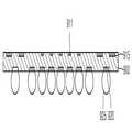
도 1a는 본 발명의 일 실시예에 따른 반도체 패키지의 단면도이다. 도 1b는 도 1a의 평면도를 도시한 것이다. 도 1b는 도 1a의 반도체 패키지(10)의 하부 패키지(10a)의 평면도이고, 도 1a는 도 1b의 IA-IA 선에 따른 단면도이다. 도 1 및 도 2를 참조하면, 반도체 패키지(10)는 제1패키지(10a)와 제2패키지(10b)를 구비한다. 상기 제1패키지(10a)는 제1기판(100)과 상기 제1기판(100)상에 장착되는 제1반도체 칩(200)을 구비한다. 상기 제1기판(100)은 일면에 배열되는 제1랜딩 패드들(111) 및 상기 일면에 배열된 제2랜딩 패드들(115)과 상기 일면에 대향하는 타면에 배열된 제3랜딩 패드들(125)를 구비한다.1A is a cross-sectional view of a semiconductor package according to an embodiment of the present invention. Figure 1B shows a top view of Figure 1A. 1B is a plan view of the
상기 제1반도체 칩(200)은 활성면이 상기 기판(100)의 상기 일면과 대향하도록 상기 제1기판(100)상에 플립 칩 본딩되어, 솔더 볼들(210)이 상기 제1기판(100)의 상기 제1랜딩 패드들(111)과 상기 제1반도체 칩(200)의 활성면에 배열된 제1칩 패드들(215)을 전기적으로 연결시켜 줄 수 있다. 상기 제3랜딩 패드들(120)에는 외부 연결을 위한 솔더 볼들(125)이 배열될 수 있다.The
상기 제2패키지(10b)는 제2기판(150)과 제2반도체 칩(250)을 구비한다. 상기 제2기판(150)은 일면에 배열되는 본딩 패드들(160)과 상기 일면에 대향하는 타면에 배열된 제4랜딩 패드들(165)를 구비한다. 상기 제2반도체 칩(200)은 접착제(240)를 통해 상기 제2기판(150)상에 장착되어, 제2칩 패드들(260)이 상기 제2기판(150)의 본딩 패드들(160)과 와이어들(270)을 통해 전기적으로 연결된다. 상기 제4랜딩 패드들(165)에 배열된 솔더 볼들(220)이 상기 제1기판(100)의 제2랜딩 패드들(115)과 전기적으로 연결되어, 제1패키지(10a)와 제2패키지(10b)가 연결된다. 상기 제2반도 체 칩(250)과 상기 와이어들(270) 및 상기 본딩 패드들(160)과 칩 패드들(260)은 봉지부(190)에 의해 밀봉될 수 있다.The second package 10b includes a
상기 제1기판(100)의 상기 일면과 상기 제1반도체 칩(200)의 상기 활성면사이에는 언더필 물질(230)이 충진되어 상기 솔더볼들(210)을 보호한다. 상기 제1기판(100)의 상기 일면상에는 상기 언더필 물질(230)과 상기 패드 형성부(103)사이에 상기 언더필 물질(230)의 블리딩을 방지하기 위한 댐(280)이 형성된다. 상기 댐(280)은 상기 제1반도체 칩(200)을 둘러싸도록 배열될 수 있다.An
상기 댐(280)은 잉크젯 방식으로 형성되어, 표면장력에 의해 그의 상부가 라운딩지게 된다. 상기 댐(280)은 (메타)아크릴계 모노머, (메타)아크릴계 올리고머, 광개시제, 안료 및 첨가제를 함유하는 잉크 조성물을 포함할 수 있다.The
상기 (메타)아크릴계 모노머로는 일관능성 (메타)아크릴계 모노머 및 다관능성 (메타)아크릴계 모노머중에서 선택된 하나 이상을 사용한다.As the (meth) acrylic monomer, at least one selected from a monofunctional (meth) acrylic monomer and a polyfunctional (meth) acrylic monomer is used.
일관능성 (메타)아크릴계 모노머는 잉크 조성물의 점도를 작게 조절하거나 또는 잉크 조성물로 된 도막의 경도를 향상시키는 역할을 한다. 그리고 다관능성 (메타)아크릴계 모노머는 잉크 조성물의 점도를 크게 조절하거나 또는 잉크 조성물로 된 도막의 경도와 같은 물성을 향상시키는 기능을 한다.The monofunctional (meth) acrylic monomer has the role of controlling the viscosity of the ink composition to be small or improving the hardness of the coating film made of the ink composition. The polyfunctional (meth) acrylic monomer has a function of greatly controlling the viscosity of the ink composition or improving the physical properties such as the hardness of the coating film made of the ink composition.
상기 일관능성 (메타)아크릴계 모노머의 구체적인 예로서, 라우릴 아크릴레이트, 메타크릴레이트 비닐 에테르 등이 있고, 상기 다관능성 (메타)아크릴계 모노머의 구체적인 예로서, 사이클로헥산 디메탄올 디아크릴레이트, 트리스(2-하이드록시에틸)이소시아네이트 트리아크릴레이트, 에톡실레이티드 트리메틸올프로판 트리아 크릴레이트 등이 있다.Specific examples of the monofunctional (meth) acrylic monomers include lauryl acrylate and methacrylate vinyl ether. Specific examples of the polyfunctional (meth) acrylic monomers include cyclohexanedimethanol diacrylate, tris 2-hydroxyethyl) isocyanate triacrylate, ethoxylated trimethylolpropane triacrylate, and the like.
상기 광개시제는 상기 잉크 조성물을 구성하는 성분들의 UV 경화반응을 개시하는 역할을 하며, 방향족 케톤 아민계 화합물을 사용한다. 이의 구체적인 예로서, 트리메틸 벤조페논, 아민 관능성 아크릴레이트, 2-메틸-1[4-(메틸티오)]페닐-2-모폴리노프로판-1-온, 이소프로필티옥산톤 등이 있다.The photoinitiator serves to initiate the UV curing reaction of the components constituting the ink composition and uses an aromatic ketone amine compound. Specific examples thereof include trimethylbenzophenone, amine functional acrylate, 2-methyl-1 [4- (methylthio)] phenyl-2-morpholinopropane-1-one and isopropyl thioxanthone.
상기 (메타)아크릴계 올리고머는 조성물내에 함유되어 점도를 조절하는 역할을 한다.The (meth) acrylic oligomer is contained in the composition to control the viscosity.
상기 안료는 잉크 조성물에 부가되어 색상을 구현하는 역할을 하며 티타늄 산화물을 사용한다. 티타늄 산화물은 Rutile의 상품명으로 상업적으로 입수가능하다.The pigment is added to the ink composition to play a role in color development and uses titanium oxide. Titanium oxide is commercially available under the trade name Rutile.
상기 첨가제로는 잉크 조성물의 안정성을 부여하여 경화를 억제하는 기능 등을 수행하는 물질로서 계면활성제 등이 있다. 상기 첨가제의 예로서, MEHQ (모노메틸 에틸 하이드로퀴논), TBHQ(터트-부틸하이드로퀴논) 등이 있다.Examples of the additive include a surfactant as a substance that performs the function of imparting stability of the ink composition to inhibit curing. Examples of the additives include MEHQ (monomethylethylhydroquinone), TBHQ (tet-butylhydroquinone), and the like.
본 발명의 일실시예에 따른 잉크 조성물에 있어서, 상기 조성물을 구성하는 각 성분의 함량은 통상적인 수준이다.In the ink composition according to an embodiment of the present invention, the content of each component constituting the composition is a conventional level.
상기 댐(280)은 기판과의 접착력 등을 고려하여 약 50 내지 100㎛ 의 폭(W)을 가지고, 15-20㎛ 의 높이(H)를 가질 수 있다. 상기 댐(280)과 상기 제1반도체 칩(200)간의 거리(D1)는 20㎛ 이상 유지하여야 한다. 이때, 상기 댐(280)을 형성하기 위한 잉크의 비산거리와 상기 제1반도체 칩(200)의 장착 마진 등을 고려하여야 하므로, 상기 거리(D1)는 약 20 내지 50㎛ 를 유지하여야 한다. 또한, 상기 댐(280)과 상기 제1랜딩 패드들(115)간의 거리(D2)는 50 ㎛ 이하로 유지될 수 있 다. 이때, 상기 댐(280)을 형성하기 위한 잉크의 비산거리를 고려하여야 하므로, 상기 거리(D2)는 댐(280)을 구성하는 물질에 따라 정해지며, 약 10 내지 50㎛ 를 유지될 수 있다.The
종래의 솔더 레지스트를 이용하여 댐을 형성하는 경우에는 그의 폭이130 내지 200㎛ 이며, 댐과 반도체 칩간의 거리가 100 내지 200㎛ 로 유지되고, 댐과 랜딩 패드들간의 거리가 50 내지 150㎛ 로 유지되었다. 그러므로, 최소한 칩과 패드간의 거리를 최소 280㎛ 로 유지하여야 하였다. 그러나, 본 발명에서는 상기 댐(280)을 잉크젯방식으로 형성함에 따라 제1반도체 칩(200)과 상기 제2랜딩 패드들(115)간의 거리를 최소 80㎛ 로 유지할 수 있다. 그러므로, 반도체 칩의 크기를 축소할 수 있으며, 상기 제1반도체 칩(200)과 상기 제2랜딩 패드들(115)간의 거리가 축소됨에 따라 패드 형성부(103)의 면적이 증가되어 제2랜딩 패드들(115)의 수를 증가시킬 수 있다. 또한, 종래의 댐 높이가 15㎛ 이하임에 반하여 본원 발명에서는 15-20㎛ 으로 댐 높이를 유지할 수 있으므로 언더필 물질의 블리딩 차단에 유리하다.When a dam is formed using a conventional solder resist, the width is 130 to 200 mu m, the distance between the dam and the semiconductor chip is maintained at 100 to 200 mu m, the distance between the dam and landing pads is 50 to 150 mu m Respectively. Therefore, at least the distance between the chip and the pad should be kept at least 280 μm. However, according to the present invention, the distance between the
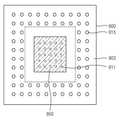
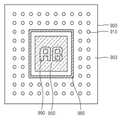
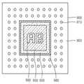
상기 댐(280)은 도 2a 내지 도 2h에 도시된 바와 같이 다양한 형태의 패턴을 포함할 수 있다. 도 2a와 같이 다중 댐 패턴(280a)을 구비하고, 도 2b 및 도 2c와 같이 상기 제1반도체 칩(200)을 둘러싸는 굴곡진 댐패턴(280b, 280c)을 구비할 수 있다. 또한, 도 2d와 같이 상기 제1반도체 칩(200)에 인접하게 배열되는 제2랜딩 패드들(115)을 각각 둘러싸는 링형상의 댐 패턴(280d)을 구비할 수 있다.The
한편, 댐(280)이 상기 제1반도체 칩(200)을 완전히 둘러싸고 배열되지 않고, 상기 제1반도체 칩(200)의 적어도 일측면에만 대응하여 댐 패턴이 배열될 수도 있다. 도 2e와 같이 상기 제1반도체 칩(200)의 상측면에 대응하여 배열되는 제2랜딩 패드들(115)을 둘러싸는 링 형상의 댐 패턴들(280e)이 배열되고, 도 2f와 같이 바 형상의 댐 패턴들(280f)이 상기 제1반도체 칩(200)의 3측면에 대응하여 배열될 수 있다.Dam patterns may be arranged corresponding to at least one side surface of the
또한, 도 2g 내지 도 2h와 같이 상기 제1반도체 칩(200)을 둘러싸는 제2랜딩 패드들(115)중 일부 제2랜딩 패드들(115)만을 그룹핑하여 보호할 수 있도록 댐 패턴들(280g, 280h)이 배열될 수도 있다. 이때, 댐 패턴들(280e, 280h)은 상기 제1반도체 칩(200)의 외곽부중 상기 언더필 물질(230)에 의해 제2랜딩 패드들(115)이 가장 손상되기 쉬운 부분, 예를 들어 상기 언더필 물질(230)이 주입되는 부분이나 언더필 물질(230)의 블리딩이 발생되기 쉬운 부분에 배열될 수 있다.As shown in FIGS. 2G to 2H,
도 3는 본 발명의 다른 실시예에 따른 반도체 패키지(20)의 단면도를 도시한 것이다. 도 3을 참조하면, 반도체 패키지(20)는 패키징 기판(300)과 상기 기판(300)의 칩 실장부에 장착된 반도체 칩(350)을 구비한다. 상기 반도체 칩(300)의 활성면상에 배열된 칩 패드들(310)은 윈도우(320)를 통해 노출되어 상기 와이어들(370)에 의해 상기 기판(300)의 일면상에 배열된 본딩 패드들(311)과 전기적으로 연결된다. 상기 기판(300)의 상기 일면상에 배열된 랜딩 패드들(315)은 외부 연결용 솔더 볼들(325)과 전기적으로 연결된다.3 shows a cross-sectional view of a
상기 랜딩 패드들(315)과 상기 본딩 패드들(311)사이의 상기 기판(300)의 상기 일면상에는 댐(280)이 배열된다. 상기 댐(280)은 잉크젯방식에 의해 형성되어, 소정 높이(H)과 소정 폭(W)을 가질 수 있다. 상기 댐(280)은 상기 본딩 패드들(311)과는 제1거리(D1)를 두고 배열되고, 상기 랜딩 패드들(315)과는 제2거리(D2)를 두고 배열될 수 있다. 상기 댐(280)은 도 2a 내지 도 2c와 같은 패턴을 포함할 수 있다. 상기 윈도우(320)에 의해 노출되는 상기 반도체 칩(350)의 상기 활성면 그리고 상기 댐(280)사이의 상기 기판(200)의 일면상에는 언더필 물질이 충진된다.A
도 4는 본 발명의 또 다른 실시예에 따른 반도체 패키지의 단면도를도시한 것이다. 도 4를 참조하면, 반도체 패키지(30)는 기판(400)과 상기 기판(400)의 일면상에 적층된 반도체 칩들(450, 455)을 구비한다. 상기 제1반도체 칩(450)은 접착제(440)에 의해 상기 기판(400)의 일면상에 장착되고, 상기 제1반도체 칩(450)의 활성면에 배열된 제1칩 패드들(460)은 상기 기판(400)의 상기 일면상에 배열된 본딩 패드들(415)과 전기적으로 연결된다. 상기 기판(400)의 타면상에 배열된 랜딩 패드들(420)에는 외부 연결용 솔더 볼들(425)이 배열될 수 있다.4 is a cross-sectional view of a semiconductor package according to another embodiment of the present invention. Referring to FIG. 4, the
상기 제1반도체 칩(450)의 상기 활성면과 상기 제2반도체 칩(455)의활성면이 서도 대향하도록 배열되어, 상기 제1반도체 칩(450)의 제1랜딩 패드들(465)이 상기 제2반도체칩(455)의 제2랜링 패드들(457)과 솔더 볼(467)을 통해 전기적으로 연결될 수 있다. 상기 제2반도체 칩(455)과 상기 제1반도체 칩(450)사이에는 언더필 물질(430)이 충진되어 상기 솔더 볼들(467)을 보호하게 된다.The active surfaces of the
상기 제2반도체 칩(455)과 상기 본딩 패드(460)사이의 상기 제1반도체 칩(450)의 상기 활성면상에는 댐(480)이 배열된다. 상기 댐(480)은 잉크젯방식에 의해 형성되어, 소정 높이(H)과 소정 폭(W)을 가질 수 있다. 상기 댐(480)은 상기 제2반도체 칩(455)과는 상기 제1거리(D1)를 두고 배열되고, 상기 본딩 패드들(460)과는 상기 제2거리(D2)를 두고 배열될 수 있다. 상기 댐(480)은 도 2a 내지 도 2c와 같은 패턴을 포함할 수 있다. 상기 기판(400)상에는 밀봉수지(490)가 배열되어 상기 반도체 칩들(450, 455), 댐(480) 및 와이어들(470)과 패드들(460, 415)을 보호할 수 있다.A
도 5a 및 도 5b는 본 발명의 또 다른 실시예에 따른 반도체 패키지(40)의 단면도 및 평면도를 도시한 것이다. 도 5a는 도 5b의 VA-VA 선에 따른 단면도이다. 도 5a 및 도 5b를 참조하면, 기판(500)의 칩 실장부에 제1반도체 칩(550)과 제2반도체 칩(555)이 적층된다. 상기 제1반도체 칩(550)과 상기 제2반도체 칩(555)은 활성면에 대향하는 면들이 접착제(540)를 통해 접착된다.5A and 5B show cross-sectional and plan views of a
상기 제1반도체 칩(550)의 상기 활성면에 배열된 제1랜딩 패드들(560)은 상기 기판(500)의 일면상에 배열된 랜딩 패드들(511)과 솔더 볼들(567)을 통해 전기적으로 연결되고, 상기 제2반도체 칩(555)의 상기 활성면에 배열된 본딩 패드들(565)은 와이어(570)를 통해 상기 기판(500)의 상기 일면에 배열된 본딩 패드들(515)과 전기적으로 연결된다. 상기 기판(500)의 타면에 배열된 랜딩 패드들(520)에는 솔더 볼들(525)이 배열될 수 있다.The
상기 제1반도체 칩(550)과 상기 기판(500)의 상기 일면사이에는 언더필 물질(530)이 충진된다. 상기 본딩 패드들(515)은 윈도우(515a)를 통해 노출되고, 댐(580)이 상기 제1반도체 칩(550)과 상기 윈도우들(515a)사이에만 부분적으로 형 성될 수도 있다. 상기 댐(580)은 상기 윈도우(515a)를 둘러싸도록 배열될 수 있다. 상기 댐(580)은 잉크젯방식에 의해 형성되어, 소정 높이(H)과 소정 폭(W)을 가질 수 있다. 상기 댐(580)은 상기 제1반도체 칩(550)과는 상기 제1거리(D1)를 두고 배열되고, 상기 윈도우(515a)와는 제2거리(D2)를 두고 배열될 수 있다. 상기 댐(580)은 도 2a-도 2c 및 도 2f-도 2i와 같은 패턴을 포함할 수 있다.An underfill material 530 is filled between the
도 6a 및 도 6b는 본 발명의 또 다른 실시예에 따른 반도체 패키지의 단면도 및 평면도이다. 도 6a 는 도 6b의 VIA-VIA 선에 따른 단면도이다. 도 6a 및 도 6b를 참조하면, 상기 반도체 패키지(50)는 기판(600)의 일면상의 칩 실장부들에 배열된 제1반도체 칩(650)과 제2반도체 칩(655)을 구비한다. 도 6a 및 도 6b의 반도체 패키지(50)는 도 5a 및 도 5b와 반도체 패키지(40)와 상기 제1 및 제2반도체 칩들(650, 655)이 상기 기판(600)의 동일면상에 배열되는 것만이 상이하다.6A and 6B are a cross-sectional view and a plan view of a semiconductor package according to another embodiment of the present invention. 6A is a cross-sectional view taken along the line VIA-VIA in FIG. 6B. Referring to FIGS. 6A and 6B, the
도 7a 및 도 7b는 본 발명의 또 다른 실시예에 따른 반도체 패키지의 단면도 및 평면도이다. 도 7a 는 도 7b의 VII-VII 선에 따른 단면도이다. 도 7a 및 도 7b를 참조하면, 반도체 패키지(60)는 기판(700) 및 상기 기판(700)의 일면상의 칩 실장부에 배열된 제1반도체 칩(750)과 제2반도체 칩(755)을 구비한다. 상기 제1반도체 칩(750)은 인덴트(indent) 칩을 포함하고, 상기 제2반도체 칩(755)은 노말 칩을 포함할 수 있다.7A and 7B are a cross-sectional view and a plan view of a semiconductor package according to another embodiment of the present invention. FIG. 7A is a cross-sectional view taken along line VII-VII of FIG. 7B. FIG. 7A and 7B, a
상기 제1반도체 칩(750)의 제1칩 패드들(761)이 와이어들(770)을 통해 상기 기판(700)의 본딩 패드들(711)과 전기적으로 연결되고, 상기 제2반도체 칩(755)의 제2칩 패드들(765)은 솔더볼(767)을 통해 상기 기판(700)의 랜딩 패드들(715)과 전 기적으로 연결될 수 있다. 상기 제2반도체 칩(755)과 상기 기판(700)의 상기 일면사이에는 언더필 물질(730)이 충진되고, 댐(780)이 상기 제1반도체 칩(750)의 인덴트부(751)과 상기 제2반도체 칩(755)사이에만 부분적으로 배열될 수도 있다. 한편, 상기 댐(780)은 상기 제2반도체 칩(750)을 둘러싸도록 배열될 수 있다.The
도 8은 본 발명의 또 다른 실시예에 따른 반도체 패키지의 제조방법을 설명하기 위한 공정 순서도이다. 도 9a 내지 제12a는 도 8의 반도체 패키지의 제조방법을 설명하기 위한 평면도이다. 도 9b 내지 도 12b는 도 8의 반도체 패키지의 제조방법을 설명하기 위한 단면도로서, 도 9a의 B-B 선에 따른 단면도를 도시한 것이다. 도 8, 도 9a-12b 및 도 9b-12b는 도 1a의 하부 패키지(10a)를 제조하는 방법에 한정하여 설명한다.8 is a flowchart illustrating a method of manufacturing a semiconductor package according to another embodiment of the present invention. FIGS. 9A to 12A are plan views for explaining the method of manufacturing the semiconductor package of FIG. 9B to 12B are cross-sectional views illustrating a method of manufacturing the semiconductor package of FIG. 8, which are cross-sectional views taken along line B-B of FIG. 9A. Figs. 8, 9A-12B, and 9B-12B illustrate only the method of manufacturing the
도 8과 도 9a 및 도 9b를 참조하면, 기판(900)을 제작한다(S810). 상기 기판(900)은 PCB(printed circuit board) 또는 테이프 배선 기판 등을 포함할 수 있다. 상기 기판(900)은 반도체 칩(도 10a 및 도 10b의 950)이 배열될 칩 실장부(901)과 상기 칩 실장부(901)의 외곽부에 배열되는 패드 형성부(903)을 포함한다. 상기 칩 실장부(901)에 배열되는 패드들(911)은 상기 반도체 칩(950)과의 전기적 연결을 위한 패드들이다. 상기 패드 형성부(903)에는 다수의 패드들(915)이 배열된다. 상기 패드들(915)은 와이어 본딩을 위한 본딩 패드들 또는 솔더 볼 부착을 위한 랜딩 패드들을 포함할 수 있다.8 and 9A and 9B, a
도 8과 도 10a 및 도 10b를 참조하면, 상기 제조된 기판(900)의 상기 칩 실장부(901)에 상기 반도체 칩(950)을 실장한다(S820). 상기 반도체 칩(950)은 상기 기판(900)에 플립 칩 본딩될 수 있다. 상기 반도체 칩(950)의 칩 패드들(960)에 미리 부착된 솔더 볼들(967)을 통해 상기 칩 패드들(960)과 상기 패드들(911)을 전기적으로 연결시켜 줄 수 있다.Referring to FIGS. 8 and 10A and 10B, the
도 8과 도 11a 및 도 11b를 참조하면, 잉크젯 공정을 수행하여 상기 반도체 칩(950)과 상기 패드 형성부(903)사이의 상기 기판(900)의 상기 일면상에 댐(980)을 형성한다(S830). 상기 댐(980)은 도 2a 내지 도 2i와 같은 형상으로 배열될 수 있다. 상기 잉크젯 공정을 통한 상기 댐(980)을 형성하는 공정(S830)에서, 상기 반도체 칩(950)상에 패키지의 종류 및 특성등을 표시하는 문자(990)를 마킹할 수도 있다. 상기 마킹 및 댐 형성공정후 상기 문자(990)와 상기 댐(980)을 경화시켜 주는 공정을 더 수행할 수 있다. 상기 경화공정은 UV 또는 열경화공정을 수행할 수도 있다.8 and 11A and 11B, an inkjet process is performed to form a
상기 댐(980)을 형성한 다음 마킹을 하거나 또는 마킹을 한 다음 상기 댐(980)을 형성할 수도 있다. 또한, 상기 댐(980)의 형성과 상기 문자(990)의 마킹을 동시에 할 수도 있다. 상기 댐(980)은 상기 문자(990)와 동일 재질로 이루어지거나, 서로 다른 재질로 이루어질 수도 있다.The
도 8과 도 12a 및 도 12b를 참조하면, 상기 반도체 칩(950)의 활성면과 상기 기판(900)의 상기 일면사이에 언더필 물질(930)을 충진시켜 준다(S840). 상기 언더필 물질(930)은 상기 솔더 볼(967)을 보호하고, 상기 댐(980)에 의해 상기 패드들(915)로의 블리딩은 방지된다.Referring to FIGS. 8 and 12A and 12B, an
이상 본 발명을 바람직한 실시예를 들어 상세하게 설명하였으나, 본 발명은 상기 실시예에 한정되지 않고, 본 발명의 기술적 사상의 범위 내에서 당 분야에서 통상의 지식을 가진 자에 의하여 여러가지 변형이 가능하다.While the present invention has been particularly shown and described with reference to exemplary embodiments thereof, it is to be understood that the invention is not limited to the disclosed exemplary embodiments, but many variations and modifications may be made by those skilled in the art .
도 1a는 본 발명의 일 실시예에 따른 반도체 패키지의 단면도이다.1A is a cross-sectional view of a semiconductor package according to an embodiment of the present invention.
도 1b는 도 1a의 반도체 패키지의 하부 패키지의 평면도이다.1B is a plan view of the lower package of the semiconductor package of FIG. 1A.
도 2a 내지 도 2h는 도 1a 및 lb의 반도체 패키지의 댐의 구조를 도시한 것이다.2A to 2H show the structure of the dam of the semiconductor package of FIGS. 1A and 1B.
도 3은 본 발명의 다른 실시예에 따른 반도체 패키지의 단면도이다.3 is a cross-sectional view of a semiconductor package according to another embodiment of the present invention.
도 4는 본 발명의 또 다른 실시예에 따른 반도체 패키지의 단면도이다.4 is a cross-sectional view of a semiconductor package according to another embodiment of the present invention.
도 5a는 본 발명의 또 다른 실시예에 따른 반도체 패키지의 단면도이다.5A is a cross-sectional view of a semiconductor package according to another embodiment of the present invention.
도 5b는 도 5a의 또 다른 실시예에 따른 반도체 패키지의 평면도이다.5B is a plan view of a semiconductor package according to another embodiment of FIG. 5A.
도 6a는 본 발명의 또 다른 실시예에 따른 반도체 패키지의 단면도이다.6A is a cross-sectional view of a semiconductor package according to another embodiment of the present invention.
도 6b는 도 6a의 또 다른 실시예에 따른 반도체 패키지의 평면도이다.6B is a plan view of a semiconductor package according to another embodiment of FIG. 6A.
도 7a는 본 발명의 또 다른 실시예에 따른 반도체 패키지의 단면도이다.7A is a cross-sectional view of a semiconductor package according to another embodiment of the present invention.
도 7b는 도 7a의 또 다른 실시예에 따른 반도체 패키지의 평면도이다.7B is a plan view of a semiconductor package according to another embodiment of FIG. 7A.
도 8은 본 발명의 또 다른 실시예에 따른 반도체 패키지의 제조방법을 설명하기 위한 공정 순서도이다.8 is a flowchart illustrating a method of manufacturing a semiconductor package according to another embodiment of the present invention.
도 9a 내지 도 12a는 도 8의 반도체 패키지의 제조방법을 설명하기위한 평면도들이다.9A to 12A are plan views for explaining a method of manufacturing the semiconductor package of FIG.
도 9b 내지 도 12b는 도 8의 반도체 패키지의 제조방법을 설명하기 위한 단면도들이다.FIGS. 9B to 12B are cross-sectional views illustrating a method of manufacturing the semiconductor package of FIG.
Claims (10)
Translated fromKoreanPriority Applications (4)
| Application Number | Priority Date | Filing Date | Title |
|---|---|---|---|
| KR20080095519AKR101481577B1 (en) | 2008-09-29 | 2008-09-29 | Semiconductor package having dam of ink jet method and manufacturing method thereof |
| US12/547,662US7999368B2 (en) | 2008-09-29 | 2009-08-26 | Semiconductor package having ink-jet type dam and method of manufacturing the same |
| JP2009225170AJP2010087516A (en) | 2008-09-29 | 2009-09-29 | Semiconductor package having ink-jet type dam and method of manufacturing the same |
| US13/182,588US8187921B2 (en) | 2008-09-29 | 2011-07-14 | Semiconductor package having ink-jet type dam and method of manufacturing the same |
Applications Claiming Priority (1)
| Application Number | Priority Date | Filing Date | Title |
|---|---|---|---|
| KR20080095519AKR101481577B1 (en) | 2008-09-29 | 2008-09-29 | Semiconductor package having dam of ink jet method and manufacturing method thereof |
Publications (2)
| Publication Number | Publication Date |
|---|---|
| KR20100036073A KR20100036073A (en) | 2010-04-07 |
| KR101481577B1true KR101481577B1 (en) | 2015-01-13 |
Family
ID=42056507
Family Applications (1)
| Application Number | Title | Priority Date | Filing Date |
|---|---|---|---|
| KR20080095519AActiveKR101481577B1 (en) | 2008-09-29 | 2008-09-29 | Semiconductor package having dam of ink jet method and manufacturing method thereof |
Country Status (3)
| Country | Link |
|---|---|
| US (2) | US7999368B2 (en) |
| JP (1) | JP2010087516A (en) |
| KR (1) | KR101481577B1 (en) |
Families Citing this family (69)
| Publication number | Priority date | Publication date | Assignee | Title |
|---|---|---|---|---|
| US20130026609A1 (en)* | 2010-01-18 | 2013-01-31 | Marvell World Trade Ltd. | Package assembly including a semiconductor substrate with stress relief structure |
| US20110186960A1 (en) | 2010-02-03 | 2011-08-04 | Albert Wu | Techniques and configurations for recessed semiconductor substrates |
| JP5589620B2 (en)* | 2010-07-01 | 2014-09-17 | 日本電気株式会社 | Electronic component cooling structure, electronic component device, heat sink |
| KR101088088B1 (en) | 2010-08-17 | 2011-11-30 | 앰코 테크놀로지 코리아 주식회사 | Manufacturing method of stacked semiconductor package |
| JP5537341B2 (en)* | 2010-08-31 | 2014-07-02 | 株式会社東芝 | Semiconductor device |
| CN102451808B (en)* | 2010-10-18 | 2015-01-07 | 展晶科技(深圳)有限公司 | Phosphor coating method |
| TWI424552B (en)* | 2010-12-31 | 2014-01-21 | Ind Tech Res Inst | Three dimensional chip stacking package structure |
| KR101222820B1 (en)* | 2011-03-16 | 2013-01-15 | 삼성전기주식회사 | Semiconductor package and manufacturing method of the same |
| US20130093072A1 (en)* | 2011-10-13 | 2013-04-18 | Stmicroelectronics Pte Ltd. | Leadframe pad design with enhanced robustness to die crack failure |
| US8597982B2 (en)* | 2011-10-31 | 2013-12-03 | Nordson Corporation | Methods of fabricating electronics assemblies |
| US9025339B2 (en)* | 2011-12-29 | 2015-05-05 | Stmicroelectronics Pte Ltd. | Adhesive dam |
| US20150192281A1 (en)* | 2012-07-09 | 2015-07-09 | Sharp Kabushiki Kaisha | Light emission device, and illumination device |
| US9136236B2 (en) | 2012-09-28 | 2015-09-15 | Intel Corporation | Localized high density substrate routing |
| US9312193B2 (en)* | 2012-11-09 | 2016-04-12 | Taiwan Semiconductor Manufacturing Company, Ltd. | Stress relief structures in package assemblies |
| JP6125209B2 (en)* | 2012-11-19 | 2017-05-10 | 株式会社ジェイデバイス | Semiconductor device and manufacturing method thereof |
| KR20140066518A (en)* | 2012-11-23 | 2014-06-02 | 삼성전자주식회사 | Semiconductor device and method for fabricating the same |
| US9497861B2 (en)* | 2012-12-06 | 2016-11-15 | Taiwan Semiconductor Manufacturing Company, Ltd. | Methods and apparatus for package with interposers |
| US8994176B2 (en) | 2012-12-13 | 2015-03-31 | Taiwan Semiconductor Manufacturing Company, Ltd. | Methods and apparatus for package with interposers |
| JP5930070B2 (en) | 2012-12-28 | 2016-06-08 | 富士電機株式会社 | Semiconductor device |
| EP2966680B1 (en)* | 2013-03-07 | 2024-08-28 | Tohoku-Microtec Co., Ltd | Stacked device and method of producing same |
| US9165876B2 (en)* | 2013-03-11 | 2015-10-20 | Taiwan Semiconductor Manufacturing Company, Ltd. | Package-on-package structure and methods for forming the same |
| KR102076050B1 (en) | 2013-03-29 | 2020-02-12 | 삼성전자주식회사 | Stack type semiconductor package |
| US9000599B2 (en)* | 2013-05-13 | 2015-04-07 | Intel Corporation | Multichip integration with through silicon via (TSV) die embedded in package |
| KR102076047B1 (en) | 2013-06-25 | 2020-02-11 | 삼성전자주식회사 | package for semiconductor devices and manufacturing method of the same |
| US9627229B2 (en)* | 2013-06-27 | 2017-04-18 | STATS ChipPAC Pte. Ltd. | Semiconductor device and method of forming trench and disposing semiconductor die over substrate to control outward flow of underfill material |
| US10192810B2 (en)* | 2013-06-28 | 2019-01-29 | Intel Corporation | Underfill material flow control for reduced die-to-die spacing in semiconductor packages |
| CN103390563B (en)* | 2013-08-06 | 2016-03-30 | 江苏长电科技股份有限公司 | Erosion flip-chip of being first honored as a queen three-dimensional systematic metal circuit board structure &processes method |
| CN103489792B (en)* | 2013-08-06 | 2016-02-03 | 江苏长电科技股份有限公司 | First be honored as a queen and lose three-dimensional systematic flip chip encapsulation structure and process |
| DE112013007722B4 (en)* | 2013-12-27 | 2024-11-28 | Google Llc | Optoelectronic packaging assemblies |
| JP6379799B2 (en)* | 2014-01-24 | 2018-08-29 | 富士電機株式会社 | Semiconductor device |
| US9887104B2 (en)* | 2014-07-03 | 2018-02-06 | Intel Corporation | Electronic package and method of connecting a first die to a second die to form an electronic package |
| US9972557B2 (en) | 2014-12-11 | 2018-05-15 | Stmicroelectronics Pte Ltd | Integrated circuit (IC) package with a solder receiving area and associated methods |
| JP6430843B2 (en)* | 2015-01-30 | 2018-11-28 | 株式会社ジェイデバイス | Semiconductor device |
| TWI582916B (en)* | 2015-04-27 | 2017-05-11 | 南茂科技股份有限公司 | Multi chip package structure, wafer level chip package structure and manufacturing method thereof |
| US9741633B2 (en) | 2015-06-02 | 2017-08-22 | Samsung Electronics Co., Ltd. | Semiconductor package including barrier members and method of manufacturing the same |
| CN104916593A (en)* | 2015-06-02 | 2015-09-16 | 三星半导体(中国)研究开发有限公司 | Package and method of manufacturing package |
| JP6591234B2 (en)* | 2015-08-21 | 2019-10-16 | ルネサスエレクトロニクス株式会社 | Semiconductor device |
| US9576942B1 (en)* | 2015-12-18 | 2017-02-21 | Intel Corporation | Integrated circuit assembly that includes stacked dice |
| JP2017123446A (en)* | 2016-01-08 | 2017-07-13 | 株式会社日立製作所 | Semiconductor device and semiconductor package device |
| US9896330B2 (en) | 2016-01-13 | 2018-02-20 | Texas Instruments Incorporated | Structure and method for packaging stress-sensitive micro-electro-mechanical system stacked onto electronic circuit chip |
| TWI602275B (en)* | 2016-10-14 | 2017-10-11 | 恆勁科技股份有限公司 | Package structure and its fabrication method |
| CN109804464B (en)* | 2016-10-21 | 2023-07-18 | 索尼半导体解决方案公司 | Electronic substrate and electronic device |
| US11676929B2 (en) | 2016-10-21 | 2023-06-13 | Sony Semiconductor Solutions Corporation | Electronic substrate and electronic apparatus |
| WO2018125166A1 (en)* | 2016-12-29 | 2018-07-05 | Intel Corporation | Package with underfill containment barrier |
| JP2018137305A (en)* | 2017-02-21 | 2018-08-30 | 富士通コンポーネント株式会社 | Electronic device and manufacturing method thereof |
| US10586716B2 (en) | 2017-06-09 | 2020-03-10 | Advanced Semiconductor Engineering, Inc. | Semiconductor device package |
| US10861741B2 (en)* | 2017-11-27 | 2020-12-08 | Texas Instruments Incorporated | Electronic package for integrated circuits and related methods |
| US11538767B2 (en) | 2017-12-29 | 2022-12-27 | Texas Instruments Incorporated | Integrated circuit package with partitioning based on environmental sensitivity |
| US10510694B2 (en)* | 2018-04-18 | 2019-12-17 | Analog Devices, Inc. | Radio frequency communication systems |
| JP2020053563A (en) | 2018-09-27 | 2020-04-02 | イビデン株式会社 | Printed wiring board and method of manufacturing the same |
| US20200118940A1 (en)* | 2018-10-15 | 2020-04-16 | Intel Corporation | Die with bumper for solder joint reliability |
| US10796976B2 (en) | 2018-10-31 | 2020-10-06 | Taiwan Semiconductor Manufacturing Company, Ltd. | Semiconductor device and method of forming the same |
| US10629455B1 (en)* | 2018-11-20 | 2020-04-21 | Nanya Technology Corporation | Semiconductor package having a blocking dam |
| JP2020123604A (en)* | 2019-01-29 | 2020-08-13 | 富士通コンポーネント株式会社 | Electronic device |
| KR102565715B1 (en)* | 2019-05-03 | 2023-08-10 | 삼성전자주식회사 | Semiconductor package |
| US12009271B2 (en) | 2019-07-15 | 2024-06-11 | Intel Corporation | Protruding SN substrate features for epoxy flow control |
| KR20210022911A (en)* | 2019-08-21 | 2021-03-04 | 삼성전기주식회사 | Semi-conductor package |
| US11450588B2 (en)* | 2019-10-16 | 2022-09-20 | Taiwan Semiconductor Manufacturing Co., Ltd. | Method for forming chip package structure with heat conductive layer |
| JP2021072423A (en)* | 2019-11-01 | 2021-05-06 | イビデン株式会社 | Wiring board and manufacturing method thereof |
| US11211263B2 (en)* | 2019-11-19 | 2021-12-28 | Qualcomm Incorporated | Structure for arrayed partial molding of packages |
| KR102689648B1 (en)* | 2020-02-03 | 2024-07-30 | 삼성전자주식회사 | Semiconductor packages having dam structure |
| CN111508910B (en)* | 2020-04-21 | 2022-09-20 | 颀中科技(苏州)有限公司 | Flip chip packaging structure and packaging method |
| US11664340B2 (en)* | 2020-07-13 | 2023-05-30 | Analog Devices, Inc. | Negative fillet for mounting an integrated device die to a carrier |
| US11443997B2 (en)* | 2020-07-20 | 2022-09-13 | Advanced Semiconductor Engineering, Inc. | Semiconductor package and method of manufacturing the same |
| US11688657B2 (en) | 2021-02-10 | 2023-06-27 | Amkor Technology Singapore Holding Pte. Ltd. | Semiconductor devices and methods of manufacturing semiconductor devices |
| KR20230010399A (en)* | 2021-07-12 | 2023-01-19 | 삼성전자주식회사 | Semiconductor package |
| US12040285B2 (en)* | 2021-08-30 | 2024-07-16 | Taiwan Semiconductor Manufacturing Company, Ltd. | Structure and formation method of chip package with reinforcing structures |
| US20230086920A1 (en)* | 2021-09-21 | 2023-03-23 | Intel Corporation | Dam surrounding a die on a substrate |
| CN116230650A (en)* | 2023-03-02 | 2023-06-06 | 上海韬润半导体有限公司 | Packaging structure and packaging method |
Citations (4)
| Publication number | Priority date | Publication date | Assignee | Title |
|---|---|---|---|---|
| US6400036B1 (en)* | 2000-06-03 | 2002-06-04 | Siliconware Precision Industries Co., Ltd. | Flip-chip package structure and method of fabricating the same |
| US20030090006A1 (en) | 2000-08-08 | 2003-05-15 | Farnworth Warren M. | Underfill and encapsulation of carrier substrate-mounted flip-chip components using stereolithography |
| KR20070009607A (en)* | 2004-04-12 | 2007-01-18 | 옵토팩 주식회사 | Electronic package having sealing structure on predetermined area and method |
| KR20070017671A (en)* | 2005-08-08 | 2007-02-13 | 삼성전기주식회사 | A Flip Chip Semiconductor Package |
Family Cites Families (7)
| Publication number | Priority date | Publication date | Assignee | Title |
|---|---|---|---|---|
| KR20010010131A (en) | 1999-07-16 | 2001-02-05 | 윤종용 | Method for fabricating chip on board package |
| EP1078761B1 (en)* | 1999-08-27 | 2008-10-29 | Océ-Technologies B.V. | Channel structure for an ink jet printhead |
| JP2002222914A (en)* | 2001-01-26 | 2002-08-09 | Sony Corp | Semiconductor device and manufacturing method therefor |
| JP2003124401A (en) | 2001-10-15 | 2003-04-25 | Nippon Avionics Co Ltd | Module and manufacturing method thereof |
| JP2004349495A (en)* | 2003-03-25 | 2004-12-09 | Seiko Epson Corp | Semiconductor device, electronic device, electronic apparatus, and method of manufacturing semiconductor device |
| US20060160917A1 (en)* | 2004-12-21 | 2006-07-20 | Seiko Epson Corporation | Ink composition |
| JP4535969B2 (en) | 2005-08-24 | 2010-09-01 | 新光電気工業株式会社 | Semiconductor device |
- 2008
- 2008-09-29KRKR20080095519Apatent/KR101481577B1/enactiveActive
- 2009
- 2009-08-26USUS12/547,662patent/US7999368B2/enactiveActive
- 2009-09-29JPJP2009225170Apatent/JP2010087516A/enactivePending
- 2011
- 2011-07-14USUS13/182,588patent/US8187921B2/enactiveActive
Patent Citations (4)
| Publication number | Priority date | Publication date | Assignee | Title |
|---|---|---|---|---|
| US6400036B1 (en)* | 2000-06-03 | 2002-06-04 | Siliconware Precision Industries Co., Ltd. | Flip-chip package structure and method of fabricating the same |
| US20030090006A1 (en) | 2000-08-08 | 2003-05-15 | Farnworth Warren M. | Underfill and encapsulation of carrier substrate-mounted flip-chip components using stereolithography |
| KR20070009607A (en)* | 2004-04-12 | 2007-01-18 | 옵토팩 주식회사 | Electronic package having sealing structure on predetermined area and method |
| KR20070017671A (en)* | 2005-08-08 | 2007-02-13 | 삼성전기주식회사 | A Flip Chip Semiconductor Package |
Also Published As
| Publication number | Publication date |
|---|---|
| US20110275177A1 (en) | 2011-11-10 |
| KR20100036073A (en) | 2010-04-07 |
| US8187921B2 (en) | 2012-05-29 |
| JP2010087516A (en) | 2010-04-15 |
| US20100078791A1 (en) | 2010-04-01 |
| US7999368B2 (en) | 2011-08-16 |
Similar Documents
| Publication | Publication Date | Title |
|---|---|---|
| KR101481577B1 (en) | Semiconductor package having dam of ink jet method and manufacturing method thereof | |
| US7564140B2 (en) | Semiconductor package and substrate structure thereof | |
| US20070132090A1 (en) | Semiconductor device | |
| US10170508B2 (en) | Optical package structure | |
| JP4423285B2 (en) | Electronic component built-in substrate and method for manufacturing electronic component built-in substrate | |
| US8455989B2 (en) | Package substrate having die pad with outer raised portion and interior recessed portion | |
| KR20010023622A (en) | Semiconductor device and method for manufacturing the same | |
| KR20040037575A (en) | Micro leadless package having oblique etching line | |
| KR100601762B1 (en) | Method for manufacturing flip chip bonding using non-conductive adhesive | |
| US6737590B2 (en) | Tape circuit board and semiconductor chip package including the same | |
| US20060103021A1 (en) | BGA package having substrate with exhaust hole | |
| KR20090108777A (en) | Substrate for semiconductor package and semiconductor package using same | |
| US20150041182A1 (en) | Package substrate and chip package using the same | |
| JPH05226505A (en) | Printed wiring board | |
| KR100780690B1 (en) | Manufacturing method of stack package | |
| KR100922370B1 (en) | Semiconductor package material | |
| KR100631997B1 (en) | Stack chip package | |
| KR100697624B1 (en) | Package substrate having surface structure for adhesive flow control and semiconductor package using same | |
| JP2006032625A (en) | Semiconductor device and manufacturing method thereof | |
| KR100197877B1 (en) | PCB Board Structure of BGA Semiconductor Package | |
| US20240249989A1 (en) | Selectively Dispensed Underfill and Edge Bond Patterns | |
| KR20100066941A (en) | Printed circuit board and semiconductor package using the same | |
| KR20010019260A (en) | PCB having dam for protecting adhesive overflow and fine pitch ball grid array(FBGA) package using the same | |
| KR20140049360A (en) | Printed circuit board | |
| KR20250115352A (en) | A circuit board and a semiconductor package including the same |
Legal Events
| Date | Code | Title | Description |
|---|---|---|---|
| PA0109 | Patent application | Patent event code:PA01091R01D Comment text:Patent Application Patent event date:20080929 | |
| PG1501 | Laying open of application | ||
| A201 | Request for examination | ||
| PA0201 | Request for examination | Patent event code:PA02012R01D Patent event date:20130709 Comment text:Request for Examination of Application Patent event code:PA02011R01I Patent event date:20080929 Comment text:Patent Application | |
| E902 | Notification of reason for refusal | ||
| PE0902 | Notice of grounds for rejection | Comment text:Notification of reason for refusal Patent event date:20140529 Patent event code:PE09021S01D | |
| E701 | Decision to grant or registration of patent right | ||
| PE0701 | Decision of registration | Patent event code:PE07011S01D Comment text:Decision to Grant Registration Patent event date:20141124 | |
| GRNT | Written decision to grant | ||
| PR0701 | Registration of establishment | Comment text:Registration of Establishment Patent event date:20150106 Patent event code:PR07011E01D | |
| PR1002 | Payment of registration fee | Payment date:20150107 End annual number:3 Start annual number:1 | |
| PG1601 | Publication of registration | ||
| FPAY | Annual fee payment | Payment date:20191226 Year of fee payment:6 | |
| PR1001 | Payment of annual fee | Payment date:20191226 Start annual number:6 End annual number:6 | |
| PR1001 | Payment of annual fee | Payment date:20201230 Start annual number:7 End annual number:7 | |
| PR1001 | Payment of annual fee | Payment date:20211229 Start annual number:8 End annual number:8 | |
| PR1001 | Payment of annual fee | Payment date:20221221 Start annual number:9 End annual number:9 | |
| PR1001 | Payment of annual fee | Payment date:20231226 Start annual number:10 End annual number:10 |