KR101479892B1 - A method of moulding - Google Patents
A method of mouldingDownload PDFInfo
- Publication number
- KR101479892B1 KR101479892B1KR20137018360AKR20137018360AKR101479892B1KR 101479892 B1KR101479892 B1KR 101479892B1KR 20137018360 AKR20137018360 AKR 20137018360AKR 20137018360 AKR20137018360 AKR 20137018360AKR 101479892 B1KR101479892 B1KR 101479892B1
- Authority
- KR
- South Korea
- Prior art keywords
- layer
- thin film
- electrical
- substrate
- trace
- Prior art date
- Legal status (The legal status is an assumption and is not a legal conclusion. Google has not performed a legal analysis and makes no representation as to the accuracy of the status listed.)
- Expired - Fee Related
Links
Images


Classifications
- H—ELECTRICITY
- H03—ELECTRONIC CIRCUITRY
- H03K—PULSE TECHNIQUE
- H03K17/00—Electronic switching or gating, i.e. not by contact-making and –breaking
- H03K17/94—Electronic switching or gating, i.e. not by contact-making and –breaking characterised by the way in which the control signals are generated
- H03K17/96—Touch switches
- H03K17/962—Capacitive touch switches
- H03K17/9622—Capacitive touch switches using a plurality of detectors, e.g. keyboard
- H—ELECTRICITY
- H05—ELECTRIC TECHNIQUES NOT OTHERWISE PROVIDED FOR
- H05K—PRINTED CIRCUITS; CASINGS OR CONSTRUCTIONAL DETAILS OF ELECTRIC APPARATUS; MANUFACTURE OF ASSEMBLAGES OF ELECTRICAL COMPONENTS
- H05K3/00—Apparatus or processes for manufacturing printed circuits
- H05K3/10—Apparatus or processes for manufacturing printed circuits in which conductive material is applied to the insulating support in such a manner as to form the desired conductive pattern
- B—PERFORMING OPERATIONS; TRANSPORTING
- B32—LAYERED PRODUCTS
- B32B—LAYERED PRODUCTS, i.e. PRODUCTS BUILT-UP OF STRATA OF FLAT OR NON-FLAT, e.g. CELLULAR OR HONEYCOMB, FORM
- B32B37/00—Methods or apparatus for laminating, e.g. by curing or by ultrasonic bonding
- B32B37/14—Methods or apparatus for laminating, e.g. by curing or by ultrasonic bonding characterised by the properties of the layers
- B32B37/16—Methods or apparatus for laminating, e.g. by curing or by ultrasonic bonding characterised by the properties of the layers with all layers existing as coherent layers before laminating
- B32B37/18—Methods or apparatus for laminating, e.g. by curing or by ultrasonic bonding characterised by the properties of the layers with all layers existing as coherent layers before laminating involving the assembly of discrete sheets or panels only
- B—PERFORMING OPERATIONS; TRANSPORTING
- B29—WORKING OF PLASTICS; WORKING OF SUBSTANCES IN A PLASTIC STATE IN GENERAL
- B29C—SHAPING OR JOINING OF PLASTICS; SHAPING OF MATERIAL IN A PLASTIC STATE, NOT OTHERWISE PROVIDED FOR; AFTER-TREATMENT OF THE SHAPED PRODUCTS, e.g. REPAIRING
- B29C45/00—Injection moulding, i.e. forcing the required volume of moulding material through a nozzle into a closed mould; Apparatus therefor
- B29C45/14—Injection moulding, i.e. forcing the required volume of moulding material through a nozzle into a closed mould; Apparatus therefor incorporating preformed parts or layers, e.g. injection moulding around inserts or for coating articles
- H—ELECTRICITY
- H03—ELECTRONIC CIRCUITRY
- H03K—PULSE TECHNIQUE
- H03K17/00—Electronic switching or gating, i.e. not by contact-making and –breaking
- H03K17/94—Electronic switching or gating, i.e. not by contact-making and –breaking characterised by the way in which the control signals are generated
- H03K17/96—Touch switches
- H—ELECTRICITY
- H05—ELECTRIC TECHNIQUES NOT OTHERWISE PROVIDED FOR
- H05K—PRINTED CIRCUITS; CASINGS OR CONSTRUCTIONAL DETAILS OF ELECTRIC APPARATUS; MANUFACTURE OF ASSEMBLAGES OF ELECTRICAL COMPONENTS
- H05K7/00—Constructional details common to different types of electric apparatus
- H05K7/02—Arrangements of circuit components or wiring on supporting structure
- B—PERFORMING OPERATIONS; TRANSPORTING
- B29—WORKING OF PLASTICS; WORKING OF SUBSTANCES IN A PLASTIC STATE IN GENERAL
- B29C—SHAPING OR JOINING OF PLASTICS; SHAPING OF MATERIAL IN A PLASTIC STATE, NOT OTHERWISE PROVIDED FOR; AFTER-TREATMENT OF THE SHAPED PRODUCTS, e.g. REPAIRING
- B29C45/00—Injection moulding, i.e. forcing the required volume of moulding material through a nozzle into a closed mould; Apparatus therefor
- B29C45/14—Injection moulding, i.e. forcing the required volume of moulding material through a nozzle into a closed mould; Apparatus therefor incorporating preformed parts or layers, e.g. injection moulding around inserts or for coating articles
- B29C45/14778—Injection moulding, i.e. forcing the required volume of moulding material through a nozzle into a closed mould; Apparatus therefor incorporating preformed parts or layers, e.g. injection moulding around inserts or for coating articles the article consisting of a material with particular properties, e.g. porous, brittle
- B29C45/14811—Multilayered articles
- B—PERFORMING OPERATIONS; TRANSPORTING
- B29—WORKING OF PLASTICS; WORKING OF SUBSTANCES IN A PLASTIC STATE IN GENERAL
- B29C—SHAPING OR JOINING OF PLASTICS; SHAPING OF MATERIAL IN A PLASTIC STATE, NOT OTHERWISE PROVIDED FOR; AFTER-TREATMENT OF THE SHAPED PRODUCTS, e.g. REPAIRING
- B29C45/00—Injection moulding, i.e. forcing the required volume of moulding material through a nozzle into a closed mould; Apparatus therefor
- B29C45/16—Making multilayered or multicoloured articles
- B29C45/1671—Making multilayered or multicoloured articles with an insert
- B—PERFORMING OPERATIONS; TRANSPORTING
- B29—WORKING OF PLASTICS; WORKING OF SUBSTANCES IN A PLASTIC STATE IN GENERAL
- B29C—SHAPING OR JOINING OF PLASTICS; SHAPING OF MATERIAL IN A PLASTIC STATE, NOT OTHERWISE PROVIDED FOR; AFTER-TREATMENT OF THE SHAPED PRODUCTS, e.g. REPAIRING
- B29C53/00—Shaping by bending, folding, twisting, straightening or flattening; Apparatus therefor
- B29C53/02—Bending or folding
- B29C53/04—Bending or folding of plates or sheets
- B—PERFORMING OPERATIONS; TRANSPORTING
- B29—WORKING OF PLASTICS; WORKING OF SUBSTANCES IN A PLASTIC STATE IN GENERAL
- B29L—INDEXING SCHEME ASSOCIATED WITH SUBCLASS B29C, RELATING TO PARTICULAR ARTICLES
- B29L2031/00—Other particular articles
- B29L2031/34—Electrical apparatus, e.g. sparking plugs or parts thereof
- B29L2031/3431—Telephones, Earphones
- B29L2031/3437—Cellular phones
- B—PERFORMING OPERATIONS; TRANSPORTING
- B32—LAYERED PRODUCTS
- B32B—LAYERED PRODUCTS, i.e. PRODUCTS BUILT-UP OF STRATA OF FLAT OR NON-FLAT, e.g. CELLULAR OR HONEYCOMB, FORM
- B32B2457/00—Electrical equipment
- H—ELECTRICITY
- H03—ELECTRONIC CIRCUITRY
- H03K—PULSE TECHNIQUE
- H03K2217/00—Indexing scheme related to electronic switching or gating, i.e. not by contact-making or -breaking covered by H03K17/00
- H03K2217/94—Indexing scheme related to electronic switching or gating, i.e. not by contact-making or -breaking covered by H03K17/00 characterised by the way in which the control signal is generated
- H03K2217/96—Touch switches
- H03K2217/9607—Capacitive touch switches
- H03K2217/960755—Constructional details of capacitive touch and proximity switches
- H—ELECTRICITY
- H03—ELECTRONIC CIRCUITRY
- H03K—PULSE TECHNIQUE
- H03K2217/00—Indexing scheme related to electronic switching or gating, i.e. not by contact-making or -breaking covered by H03K17/00
- H03K2217/94—Indexing scheme related to electronic switching or gating, i.e. not by contact-making or -breaking covered by H03K17/00 characterised by the way in which the control signal is generated
- H03K2217/96—Touch switches
- H03K2217/9607—Capacitive touch switches
- H03K2217/960785—Capacitive touch switches with illumination
- Y—GENERAL TAGGING OF NEW TECHNOLOGICAL DEVELOPMENTS; GENERAL TAGGING OF CROSS-SECTIONAL TECHNOLOGIES SPANNING OVER SEVERAL SECTIONS OF THE IPC; TECHNICAL SUBJECTS COVERED BY FORMER USPC CROSS-REFERENCE ART COLLECTIONS [XRACs] AND DIGESTS
- Y10—TECHNICAL SUBJECTS COVERED BY FORMER USPC
- Y10T—TECHNICAL SUBJECTS COVERED BY FORMER US CLASSIFICATION
- Y10T29/00—Metal working
- Y10T29/49—Method of mechanical manufacture
- Y10T29/49002—Electrical device making
- Y10T29/49117—Conductor or circuit manufacturing
- Y10T29/49124—On flat or curved insulated base, e.g., printed circuit, etc.
- Y10T29/49155—Manufacturing circuit on or in base
- Y10T29/49156—Manufacturing circuit on or in base with selective destruction of conductive paths
Landscapes
- Engineering & Computer Science (AREA)
- Microelectronics & Electronic Packaging (AREA)
- Manufacturing & Machinery (AREA)
- Mechanical Engineering (AREA)
- Injection Moulding Of Plastics Or The Like (AREA)
- Shaping Of Tube Ends By Bending Or Straightening (AREA)
- Structure Of Printed Boards (AREA)
Abstract
Translated fromKoreanDescription
Translated fromKorean본 발명은 일반적으로 몰딩하는 방법과 관련된다.The present invention generally relates to a method of molding.
전자 인터페이스들은 통상적으로 컴퓨터 시스템, 게임 콘솔(game console), 전자 기기(electrical appliance), 자동차용 콘솔 또는 중앙 스택을 포함하는 차량내 시스템 및 바퀴에 탑재된 제어기, 오디오 장치를 포함하는 휴대용 장치, 멀티미디어 플레이어, 셀룰러 폰 또는 그 밖의 유사한 것을 포함하는 소비자 장치들부터 산업용 제어 콘솔, 스위치, 또는 그 밖의 유사한 것들까지 광범위한 응용들에 사용된다. 기계적 버튼, 스위치, 접속 및 그 밖의 유사한 것들이 전형적으로 종래의 전자 입력 장치들과 관련되어 사용되어 온 반면에, 기계적 버튼, 스위치 및 그 밖의 유사한 것의 이용으로부터의 변화가 터치 감응 스위치와 같은 낮은 활성화 압력 기술들을 향하여 있어 왔다. 터치 패널, 터치 스크린, 그리고 정전식 키패드(capacitive keypad) 및 그 밖의 유사한 것과 관련된 입력 장치들로의 터치 센서 기술의 통합은 정전식 센서 기술의 발달로 인하여 증가하여 왔다. 그러한 기술들은 일반적으로 디스플레이 또는 그 밖의 유사한 것들, 유리, 플라스틱, 박막 또는 그 밖의 유사한 것일 수 있고 디스플레이 위에 종종 위치되는, 과 같은 장치의 패널 상에 있는 평면 영역의 경계 내에 터치 센서 구역을 위치시킨다.Electronic interfaces typically include a computer system, a game console, an electrical appliance, an in-vehicle system including a car console or central stack and a wheel-mounted controller, a portable device including an audio device, a multimedia Consumer electronics devices, including consumer, cellular, or other similar devices, to industrial control consoles, switches, or the like. Switches, connections, and the like are typically used in connection with conventional electronic input devices, while changes from the use of mechanical buttons, switches, and the like have been associated with lower activation pressures such as touch sensitive switches Technologies. The integration of touch sensor technology into touch panels, touch screens, and input devices related to capacitive keypads and other similar has been increasing due to the development of electrostatic sensor technology. Such techniques typically place the touch sensitive area within the boundaries of the planar area on the panel of the device, such as a display or other similar, glass, plastic, thin film or other similar, and often located on the display.
그러나, 컴퓨터 스크린 및 평면 패널 입력 구역 상의 터치 감응 제어기를 사용함으로써 이득을 얻을 수 있음에도 불구하고, 몰딩된 물품으로 터치 감응 기술을 통합하는 데는 특정한 제약들이 존재한다는 것이 인정될 것이다. 현재, 장치의 원하는 모양과 관계없이, 설계는 터치 감응 입력 장치가 안으로 혹은 위로 탑재될 수 있는 평면 구역에 대한 요구에 의해 지배된다. 그 다음, 전자 및 플라스틱 부품들은 일반적으로 조립되어, 하위조립 통합, 테스트, 최종 조립, 최종 테스트 및 그 밖의 유사한 단계들을 요구하는 제품을 형성한다. 터치 감응 구역들 내에 윤곽을 갖는 형태의 구조로 쉽게 통합될 수 있는 알려진 터치 감응 스위치들 또는 다른 박막 기반의 기술들이 일반적으로 없기 때문에, 터치 감응 구역들은 평평할 것이 요구된다.However, it will be appreciated that there are certain limitations to integrating the touch sensing technology into the molded article, although it may be beneficial to use a touch sensitive controller on the computer screen and the flat panel input area. Presently, regardless of the desired shape of the device, the design is governed by the requirement for a planar area where the touch sensitive input device can be mounted in or above. The electronic and plastic parts are then assembled to form a product that requires subassembly integration, testing, final assembly, final testing, and other similar steps. Because there are generally no known touch sensitive switches or other thin film based techniques that can be easily integrated into a contoured structure within the touch sensitive areas, the touch sensitive areas are required to be flat.
최근 몇 해에, 더 좋은 인쇄 방법론들과 전기전도성(conductive) 잉크와 같은 특별한 기능을 갖는 잉크들, 및 그 밖의 유사한 것들의 발달로 인해, 박막 삽입 몰딩(Film Insert Moulding, FIM) 공정들은 터치 센서 장치 및 박막 물품과 관련된 전자발광(electoluminescent,EL) 기술을 사용한 조명 장치 등을 제조하는데 사용되어 왔다. 나아가, FIM 공정은 스위치 및 그와 유사한 것과 같은 요소들을 박막 물품에 결합하는데 사용되어 왔다. 인쇄 및 형성 공정이 완료되고 박막 물품이 생산된 후에, 인쇄된 박막 물품들은 나아가 주입 몰딩 또는 열형성 공정들을 포함하는 몰딩 공정의 대상이 될 수 있다.
In recent years, due to the development of better printing methodologies and inks with special functions such as conductive inks, and the like, Film Insert Molding (FIM) Devices and lighting devices using electoluminescent (EL) technology associated with thin film articles, and the like. Furthermore, the FIM process has been used to couple elements such as switches and the like to thin film articles. After the printing and forming process is completed and the thin film article is produced, the printed thin film articles may further be subjected to a molding process including injection molding or thermal forming processes.
예를 들어, 저항성의 그리고 차폐된 요소들은 국제출원 공개번호 WO 2009/128856에서 공개되고, 정전식 스위치는 국제출원 공개번호 WO 2008/131305에서 헤이그(Haag) 등에 공개되었다. 헤이그가 전도성 잉크들을 이용한 박막들이 형성될 수 있는 다양한 구성을 설명함에도 불구하고, 형성동안 균열의 문제가 확인되었다. 헤이그는 균열을 피하는 잉크와 관련된 변수들을 어떻게 선택하는 방법을 설명하는 데 실패했다. 헤이그는 센서 지역 내에 잉크들을 걸치는 것을 피했고, 이러한 지역 내의 균열 같은 것들에 관련된 문제를 실질적으로 해결하는 것을 제안하지는 않았다.
For example, resistive and shielded elements are disclosed in International Application Publication No. WO 2009/128856, and electrostatic switches are disclosed in Haag, et al., International Application Publication No. WO 2008/131305. Although Hague describes various configurations in which thin films can be formed using conductive inks, a problem of cracking during formation has been identified. Hague failed to explain how to choose the variables associated with the ink to avoid cracking. The Hague avoided spreading the ink in the sensor area and did not suggest to substantially solve the problems associated with such cracks in these areas.
더욱 나아가, 정전식 스위치들 및 조명 물질들이 전자 장치들에 사용되어온 동안, 종래의 FIM 정전식 터치 패널이 2차원 방식으로 가능했음에도 불구하고, 알려진 터치 감응 요소들과 조명을 박막 구조에 통합하는 것은 전도들을 게시해왔다. 도 1은 선행 기술 터치 패널(100)을 구성하는 부품들의 조립체를 보여준다. 특별히, 터치 패널(100)은 형성가능한 박막(105), 그래픽 층(104), 및 복수의 층들(101, 102, 103)을 포함할 수 있다. 복수의 층들(101, 102, 103)은 그래픽 층위에 인쇄된 전도성 잉크로 구성되어 터치 센서 지역을 형성할 수 있다. 그러나, 그러한 전도성 잉크들로부터 형성된 층들은 당해 기술 분야에서 잘 알려진 것처럼 일반적으로 잘 부러지고, 형성 공정 동안 균열되기 쉽다.
Furthermore, while conventional FIM capacitive touch panels are possible in a two-dimensional manner while electrostatic switches and lighting materials are being used in electronic devices, incorporating known touch sensitive elements and light into thin film structures I have posted evangelism. FIG. 1 shows an assembly of parts constituting the prior
제 1 측면에서 일반적인 용어들로, 본 발명은 윤곽이 만들어진 센서 지역들 내의 전도성 트랙들에서 균열의 문제를 최소화할 것을 제안한다. 이는 전자 인터페이스가 더욱 매력적이고 또는 사용자 친화적이고 또는 제조가 더욱 비용 효과적일 수 있는 이점을 가질 수 있다.
In general terms in the first aspect, the present invention proposes to minimize the problem of cracks in the conductive tracks in the outlined sensor regions. This may have the advantage that the electronic interface may be more attractive or user friendly or manufacturing may be more cost effective.
일 실시 예에서, 전도성 잉크 또는 풀(paste) 층이 기판 박막상에 인쇄되고 근접 또는 터치 센서 층을 형성하도록 처리된다. 전도성 잉크를 포함하는 투명한 접지 층 및 프라이머(primer)들이 접지를 위해 터치 센서 층위에 인쇄된다. 조명 층은 접치 증 후에 인쇄되고 처리된다. 프라이머 층은 각 층 사이의 접착을 돕고 절연을 제공할 수 있다. 접지 층은 터치 센서 층과 조명 층 사이의 간섭을 제거하거나 최소화할 수 있다. 전도성 잉크, 접지 또는 프라이머의 투과율은 조명 층으로부터 다량의 빛이 투과할 수 있도록 설정될 수 있다.
In one embodiment, a conductive ink or paste layer is printed on the substrate foil and processed to form a proximity or touch sensor layer. A transparent ground layer and primers containing conductive ink are printed on the touch sensor layer for grounding. The illumination layer is printed and processed after the folding. The primer layer can aid adhesion between the layers and provide insulation. The ground layer can eliminate or minimize interference between the touch sensor layer and the illumination layer. The transmittance of the conductive ink, ground, or primer can be set such that a large amount of light can be transmitted from the illumination layer.
제 2 측면에서, 본 발명은 박막 삽입 몰딩된 인터페이스와 제어기 사이의 상호 연결을 제안하되, 상호 연결은:In a second aspect, the invention proposes an interconnection between a thin film insert molded interface and a controller, wherein the interconnection comprises:
전도성 잉크 회로 또는 연결선,Conductive ink circuit or connection line,
측면(side) 벽상에 접착되고, 외표면과 평행하거나 근접한 이방성의 전도성 박막,Anisotropic conductive thin films adhered on the side walls and parallel or near the outer surface,
측면 벽상에 접착되고, 압축 하중을 갖는 외표면에 평행하거나 근접한 이방성의 전도성 박막,An anisotropic conductive thin film adhered on the side wall and parallel or near to the outer surface having a compressive load,
장식용 표면의 뒤에 접착된 이방성의 전도성 박막,An anisotropic conductive thin film adhered to the back of the decorative surface,
탄성 중합체 잠금부(elastomeric fastening)를 갖는 장식용 표면 뒤에 접착된 이방성의 전도성 박막,An anisotropic conductive thin film adhered to the decorative surface with an elastomeric fastening,
측면 벽상에 접착되고, 외표면과 수직하거나 근접한 이방성의 전도성 박막,An anisotropic conductive thin film adhered on the side wall and perpendicular or close to the outer surface,
장식용 표면 뒤의 탄성 중합체 커넥터,Elastomeric connectors behind decorative surfaces,
외표면에 평행사거나 근접한, 측면 벽상의 탄성 중합체 커넥터,로 구성된 집단으로부터 선택된다.
An elastomeric connector on the side wall that is flat or adjacent to the outer surface.
제 3 측면에서, 본 발명은 촉각 피드백을 포함하는 터치 또는 근접 센서들을 갖는 박막 삽입 몰딩된 전자 인터페이스를 제안하되, 촉각 피드백은: 센서들의 빛, 센서의 임계 질량/무게, 센서의 거침/질감, 점성/감쇠, 단단함/디텐트(detent), 펄스, 파형, 진동 및 그것들의 어떤 조합으로 구성된 집단으로부터 선택된다.
In a third aspect, the invention proposes a thin film insert molded electronic interface with touch or proximity sensors comprising tactile feedback, wherein the tactile feedback comprises: light of the sensors, critical mass / weight of the sensor, Viscosity / attenuation, rigidity / detent, pulse, waveform, vibration, and any combination thereof.
본 발명의 특정한 표현에서, 청구항 1에서 요구된 것과 같은 방법이 제공된다. 실시 예들은 청구항 2 내지 18 중 하나에 따라 구현될 수 있다.
In a particular expression of the invention, a method as claimed in
일 실시 예에서, 표면 특성은 박막의 전처리에 의해 또는 표면 코팅 등: 뿌리기, 담그기 또는 플라스틱 몰딩 공정 전 마스터-배치(master-batch)를 추가하는 것과 같은 혼합물 통합, 에 의해 수행될 수 있다.
In one embodiment, the surface properties may be performed by pretreatment of the thin film or by surface consolidation, such as by spraying, immersion, or by incorporating a mixture such as adding a master-batch prior to the plastic molding process.
비한정적인 예들을 통해 본 발명의 실시 예들이 완전하고 더욱 명확하게 이해될 수 있기 위해서, 이후의 설명은 유사한 참조 번호들이 유사하거나 대응하는 요소들, 지역들 및 부분들을 표시하는 첨부된 도면들과 함께 받아들여지고, 도면들에서:
도 1은 선행 기술 터치 패널을 설명하는 도면이다.
도 2a는 3차원 형태를 갖는 터치 패널 조립체의 사시도이다.
도 2b는 터치 패널 조립체의 부분 절단도이다.
도 2c는 터치 패널 조립체의 단면도이다.
도 2da는 다양한 층들을 갖는 정규의 FIM 패널 조립체를 구비한 터치의 분해도이다.
도 2db는 다양한 층들을 갖는 역(reversed) FIM 패널 조립체를 구비한 터치의 분해도이다.
도 3a는 전자 장치의 사시도이다.
도 3b는 전자 장치의 사시도이다.
도 4는 전자발광 층의 분해도이다.
도 5는 하나 이상의 실시 예에 따른 전자 장치의 분해도이다.
도 6은 커넥터 조립체의 분해도이다.
도 7a는 조명 층 및 터치 센서 층을 포함하는 하나 이상의 실시 예들에 따른 전자 장치의 분해도이다.
도 7b는 터치 센서 층을 포함하는 하나 이상의 실시 예들에 따른 전자 장치의 분해도이다.
도 7c는 조명 층을 포함하는 하나 이상의 실시 예들에 따른 전자 장치의 분해도이다.
도 8-10은 연결선 상호 연결의 부분 절단도 및 분해도이다.
도 11-14는 외표면 상호 연결에 평행한(근접한), 측면 벽상의 ACF의 부분 절단도 및 분해도이다.
도 15-16은 탄성 중합체 잠금부를 갖는 장식용 표면 뒤의 ACF의 부분 절단도 및 분해도이다.
도 17-18은 장식용 표면 상호 연결 뒤의 ACF의 부분 절단도 및 분해도이다.
도 19-21은 탄성 중합체 잠금부를 갖는 장식용 표면 뒤의 ACF의 부분 절단도 및 분해도이다.
도 22-25는 외표면 상호 연결에 수직인(근접한), 측면 벽상의 ACF의 부분 절단도 및 분해도이다.
도 26-27은 장식용 표면 상호 연결 뒤의 탄성 중합체 커넥터의 부분 절단도 및 분해도이다.
도 28-29는 외표면 상호 연결에 평행인(근접한), 측면 벽상의 탄성 중합체 커넥터의 부분 절단도 및 분해도이다.
도 30은 촉각 기능의 도식화 도면이다.
도 31은 3차원 형태의 박막을 제조하는 공정을 설명ㄹ하는 순서도이다.In order that the embodiments of the present invention may be understood in a non-restrictive way, the following description will be made with reference to the accompanying drawings, in which like reference numerals indicate similar or corresponding elements, Taken together, in the drawings:
1 is a view for explaining a prior art touch panel.
2A is a perspective view of a touch panel assembly having a three-dimensional shape.
2B is a partial cut-away view of the touch panel assembly.
2C is a cross-sectional view of the touch panel assembly.
2d is an exploded view of a touch with a regular FIM panel assembly having various layers.
2db is an exploded view of a touch with a reversed FIM panel assembly having various layers.
3A is a perspective view of an electronic device.
3B is a perspective view of the electronic device.
4 is an exploded view of the electroluminescent layer.
5 is an exploded view of an electronic device according to one or more embodiments.
6 is an exploded view of the connector assembly.
7A is an exploded view of an electronic device according to one or more embodiments including an illumination layer and a touch sensor layer.
7B is an exploded view of an electronic device according to one or more embodiments including a touch sensor layer.
7C is an exploded view of an electronic device according to one or more embodiments including an illumination layer.
8-10 are partial cut-away and exploded views of interconnect line interconnections.
11-14 are a partial cut-away and exploded view of an ACF on a side wall parallel (adjacent) to the outer surface interconnections.
15-16 are partial cutaway and exploded views of an ACF behind a decorative surface with an elastomeric lock.
17-18 are partial cut-away and exploded views of the ACF after decorative surface interconnections.
19-21 are partial cut-away and exploded views of an ACF behind a decorative surface with an elastomeric lock;
22-25 are partial cut-away and exploded views of an ACF on a side wall perpendicular (close) to the outer surface interconnect.
Figures 26-27 are a partial cutaway and exploded view of an elastomeric connector after decorative surface interconnections.
Figs. 28-29 are partial cut-away and exploded views of elastomeric connectors on the side walls parallel (adjacent) to the outer surface interconnections.
30 is a schematic diagram of a tactile function.
FIG. 31 is a flowchart illustrating a process for manufacturing a three-dimensional thin film.
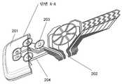
실시 예에서, 감지가 걸쳐진 윤곽들을 포함하는 트루(true) 3-D 몰딩된 물품이 도 2a 및 도 2b에서 보여진다. 터치 패널 조립체(200)는 전도성 풀로부터 만들어지는 전기층(electrical layer)과 같은 기능 층(functional layer, 202)을 갖는 몰딩된 패널(201)을 포함한다. 기능 층(202)는 전도성과 같은 특성들을 유지하는 동시에 추가적으로 유연성과 가동성을 가능하게 하도록 구성된 풀일 수 있다. FIM 공정들은 통상적으로 장식용 설계들을 인쇄하는데 사용된다; 장식용 인쇄된 표면은 실크스크린(silkscreen) 인쇄 공정 또는 잉크젯(inkjet) 인쇄에 의한 것처럼 기능 층(202)을 적용하는데 사용될 수 있다.
In an embodiment, a true 3-D molded article is shown in FIGS. 2A and 2B, which includes perceived contours. The touch panel assembly 200 includes a molded
기능 층(202)에 대한 인쇄 공정이 완료된 후에, 기능 층(202)은 몰딩된 패널(201)로 몰딩되어 터치 패널 조립체(200)를 형성하는 것과 같이 형성되고 사용될 수 있다. 초기 형성 또는 형상화는 고압 형성, 열형성 등과 같은 공정들을 포함하는 영구적으로 박막을 형상화하는 데 사용되는 공정들과 관련될 수 있다. 형성된 물품들은 그 다음 형성된 박막을 더욱 통상적인 플라스틱 패키지로 과-몰딩하는(over-mould) 데 사용될 수 있는 주입 몰딩 공정들과 같은 추가적인 몰딩의 대상이 될 수 있다.After the printing process for the
커넥터 구역들은 분해되거나 드러난 채로 남겨질 수 있다.
Connector areas may be left to disassembled or exposed.
도 2b는 도 2a의 터치 패널 조립체(200)의 절단면을 보여준다. 실시 예에서, 기능 잉크 층(202)은 복수의 전극들(203), 및 전기 회로를 형성하기 위해 전극들(203)을 연결하는 복수의 트레이스(trace, 204)들과 함께 인쇄될 수 있다. 기능 잉크 층(202)은 터치 센서 층 및/또는 조명 층일 수 있다. 기능 잉크 층(202)상의 기능 잉크는 형성 후에 전기전도성의 수용가능한 수준을 유지하는 동시에 기능 잉크 층이 형상화될 수 있도록 특정 비율 또는 비율들에 따라 잉크와 하나 이상의 구성 요소의 혼합을 제어함으로써 설정될 수 있는 잉크 물질 특성을 갖는다. 만일 기능 잉크 층이 터치 센서 층이면, 이 전기전도성의 수용가능한 수준은 터치 센서가 그것의 터치 감응 능력을 유지하는 범위이다. 만일 기능 잉크 층이 조명 층이면, 전기전도성의 수용가능한 수준은 조명 층이 빛을 방출할 수 있는 범위이다.
Figure 2b shows a cut away view of the touch panel assembly 200 of Figure 2a. In an embodiment, the
도 2c는 도 2b로부터의 단면도 A-A를 보여주고, 거기서 터치 패널 조립체(200)는 박막(205), 박막상에 인쇄된 장식용 층(206), 터치 센서 층(207) 및/또는 조명 층(208)일 수 있는 기능 잉크 층(202)을 포함할 수 있다. 터치 센서 층(207)은 예를 들어, 손가락과 같은 물체가 그곳으로 접촉 또는 근접하게 될 때 정전 용량의 변화를 감지할 수 있는 정전식 스위치를 포함하는 전기 회로처럼 구성되고 적용될 수 있다. 그러한 스위치는 값비싼 부담이 될 수 있는 움직이는 부분들의 제거 및 매우 감소된 마찰과 함께 회전식 스위치, 슬라이더(slider) 스위치, 누름 버튼 스위치 또는 그와 유사한 것들과 같은 기계적 스위치의 기능을 수행할 수 있다. 그러한 터치 센서 스위치들은 접시 세척기, 세탁기, 커피 메이커 및 그와 유사한 것들, 복사기, 실내 난방기, 오디오 시스템 및 그와 유사한 것들과 같은 가정용 기기, 아이 패드, 모바일 폰 및 그와 유사한 것들과 같은 휴대 장치, 및 오디오 시스템, 핸들 및 예를 들어 중앙 스택에 배치된 제어기와 같은 차량용 전자 시스템에서 광범위하게 사용될 수 있다. 특별히, 기능 잉크 층(202)(즉, 터치 센서 층(207) 및/또는 조명 층(208))은 균열 없이 또는 그렇지 않으면 터치 센서, 빛 방출 또는 그와 유사한 것들의 용도들에 대한 그것의 전기적인 온전함을 잃어버리지 않고, 감지 지역에 걸친 윤곽들을 포함하는 3차원 형상으로 형성되도록 유리하게 구성될 수 있다.
2C shows a cross-sectional view AA from FIG. 2B wherein the touch panel assembly 200 includes a
터치 패널 조립체의 완성 전 몰딩 공정의 구성을 더욱 잘 설명하기 위해, 도 2db는 역(reversed) FIM 구성으로 배열되거나 구조화된, 3차원 형상 을 갖는 터치 패널 조립체(200)의 분해도를 보여준다.
To better illustrate the configuration of the pre-completion molding process of the touch panel assembly, FIG. 2db shows an exploded view of the touch panel assembly 200 having a three-dimensional shape, arranged or structured in a reversed FIM configuration.
터치 패널 조립체(200)은 박막 기판(205)를 갖는다. 장식용 잉크 층(@10) 및 기능 잉크 층(202)는 박막 기판(205)상에 인쇄된다. 열가소성수지(thermoplastic) 몰딩(209)은 박막 기판(205)의 A-표면상에 몰딩된다.
The touch panel assembly 200 has a
도 2da는 정규 FIM 구성에서, 3차원 형태를 갖는 터치 패널 조립체(200)의 분해도를 도시한다. 터치 패널 조립체(200)는 박막 기판(205)을 갖는다. 장식용 잉크 층(210) 및 기능 잉크 층(202)는 박막 기판(205)상에 인쇄된다. 열가소성수지 모딩(209)은 박막 기판(205)의 B-표면상에 몰딩된다.
2d shows an exploded view of a touch panel assembly 200 having a three-dimensional shape in a regular FIM configuration. The touch panel assembly 200 has a
장식용 그래픽(210) 및 장식용 층(206)은 박막(205)상에 인쇄될 수 있고, 또는 기능 잉크 층(202)은 장식용 층(206)상에 직접적으로 인쇄될 수 있다. 어떤 예들에서, 전극들(203)은 투명하고 전도성을 갖는 것과 같은 투명한 전도성 잉크로 인쇄된다. 트레이스들(204)은 반투명 또는 불투명하다.
The decorative graphic 210 and the
다양한 층들이 조합되어 기능 물품을 형성할 수 있는 방법을 더욱 잘 설명하기 위해, 도 3a 및 3b는 일 실시 예에 따른 3차원 형태를 갖는 전자 장치(300)를 도시한다. 전자 장치(300)는 기능 잉크 층, 직접적으로 도시되지 않은, 을 포함하는 몰딩된 패널(301)을 갖는다. 인쇄되고 형성된 박막 기판은 기능 구역(303, 306)을 갖도록 몰딩될 수 있다. 기능 구역(303, 306)은 3차원 형태와 관련된 윤곽 부분에 의해 걸쳐질 수 있다. 기능 구역(303, 306) 각각은 백라이팅(backlighting) 구역(304) 및 심볼(305)를 포함할 수 있다.
To better illustrate how the various layers can be combined to form a functional article, FIGS. 3A and 3B illustrate an
박막 층(302)는 장식용 잉크 층 및 기능 잉크 층이 플라스틱 박막 기판상에 인쇄된 후에 형성될 수 있다. 예를 들어, 폴리카보네이트, 폴리에스테르 및 유사한 것들을 포함하는 열가소성수지 물질과 같이 박막 기판과 양립가능한 물질이 몰딩 공정들에 사용될 수 있다.
The
도 3b에서 보여지는 것처럼, 전자 장치(300)는 반-미생물(또는 항균성, anti-microbial) 및 유사한 것들과 같은 상이한 응용들에 따라 표면(307)의 표면 특성을 제공받을 수 있다. 예를 들어, 표면 특성은 독립적인 박막 층을 적용하는 것에 의해, 예를 들어 뿌리기 응용, 박막 응용을 통해, 또는 분자 수준에서 혼합물로서 화학적 특징을 물질 그 자체에 통합하는 것에 의해, 또는 몰딩 공간 내에 물질을 적용하는 것 또는 형성 동안 항균성 중개자, 친유성 또는 소수성 중개자 또는 그와 유사한 것들과 같은 화학 물질을 물질에 주입하는 데 사용될 수 있는 장비를 열형성하는 것에 의해 구성되거나 수정될 수 있다.
As shown in FIG. 3B, the
물질 층(311)은 그림(308)에서 보여지는 것처럼, 뿌리기 또는 그와 유사한 것들에 의한 것과 같이, 예를 들어 그림(309)에서 보여지는 것처럼 분자 주입에서 표면(307) 내에 실장될 수 있는 또는 그림(310)에서 보여지는 것처럼 표면(307)상에 분리된 채로 통합된 박막 층처럼 적용될 수 있는, 표면(307)상에 적용될 수 있다. 다양한 수정들이 당업자에게 명백할 것이다. 예를 들어, 뿌리기 응용을 대신하여, 중개자가 전자 장치(300)의 주입 몰딩 공정에서 사용되는 수지(resin)에 혼합될 수 있다. 대안적으로, 표면 특성은 독립적인 박막 층의 물질 특성과 관련될 수 있다.
The
위에서 설명된 기능 표면 층은 표면 수정을 통해 반-지문 특성, 친유성 특성 또는 그와 유사한 것을 더 포함할 수 있다. 친유성 화학 물질을 적용함으로써와 같이 전자 장치(300)의 표면(307)을 처리함으로써, 추가적인 속성이 실현될 수 있다. 예를 들어, 코팅이 전자 장치(300)상에 단단한 표면을 생성하는 데 사용되어, 그럼에도 마모, 스크래치 및 유사한 것들에 대한 저항을 증가시킬 수 있다.
The functional surface layer described above may further include anti-fingerprint properties, lipophilic properties or the like through surface modification. By processing the
어떤 예들에서, 묘사된 것과 같이, 전자 장치(300)의 표면(307)은 항균성 중개자 층으로 코팅될 수 있다. 은 기반의 중개자, 징크 피리치온(zinc pyrithione) 기반의 중개자 또는 그와 유사한 것들과 같은 중개자는 미생물, 곰팡이, 박테리아 또는 그와 유사한 것들을 죽이기 위해 적용되어 여러 사람에 의해 다루어진 물품들에 대한 교차 오염 또는 감염의 위험을 크게 감소시킬 수 있다. 항균성 효과는 항균성 중개자를 주입 몰딩 공정에서 사용되는 수지에 혼합함으로써 또는 전자 장치(300)의 표면(307)상에 직접 뿌림으로써 또는 제조 공정에서 보다 일찍 중개자를 박막 및 그와 유사한 것들에 통합함으로써 전자 장치(300) 표면상에서 달성될 수 있다.
In some instances, as depicted, the
표면은 플루오르 화학 또는 지방족 우레탄 또는 그와 유사한 것들과 같은 소수성 물질층으로 표면(307)을 코팅함으로써 쉬운 클리닝(cleaning)을 위해 더 처리될 수 있다. 소수성 표면 특성들은 물이 물품의의 표면에서 쉽게 굴러 떨어지게 하고, 그렇게 함으로써 먼지와 다른 오염물질들을 장치(300) 표면으로부터 휩쓸어간다.
The surface may be further processed for easy cleaning by coating the
상이한 층들은 형성되고 몰딩된 박막 기판에 포함될 수 있다. 조명 층(400)을 보여주는 도 4에서 열거된 것들과 같은 다양한 층들이 3차원 모양으로 형성되어 여기서 설명된 전자 제품의 제조에 사용될 수 있다. 조명 층(400)은 AC 전자발광, DC 전자발광, 유기 LED 및 그와 유사한 것들과 같은 조명 요소들로 인쇄될 수 있다.
Different layers can be formed and included in the molded thin film substrate. Various layers, such as those listed in FIG. 4 showing the
AC 전자발광(EL)을 사용하는 예시적인 조명 층(400); 조명 기능 층은 투명한 전도성 잉크(401), 인광체(phosphor) 잉크 층(402), 3개 층 이상의 유전체 잉크 층(403), 제 2 전도성 잉크 층(404) 및 투명한 프라이머 잉크(405)로 구성될 수 있다. 인광체 잉크 층(402)는 전도성 잉크 층(401)과 유전체 잉크 층(403) 사이에 끼워지고, 유전체 잉크 층(403)은 선택적 전류가 인가될 때, 인광체 잉크 층(402)이 빛을 방출하게 하는 전극으로서 기능한다. 인을 함유한 잉크 층(402)는 지르콘 황화물 또는 그와 유사한 것과 같은 어떤 인광체 물질로 인쇄될 수 있고, 인광체 물질은 전기적 전류가 인가될 때 빛을 방출한다. 유전체 층(403)은 EL 응용과 호환가능한 어떤 유전체 잉크들로 인쇄된다. 은 전도성 잉크 층(404)는 전기 전도에 사용되는 EL 층에 대한 제 2 또는 후방 전극으로서 기능한다. 유전체 층은 은 전도성 잉크 층 위에 인쇄되어 주입 몰딩 및 처리 동안에 은 회로를 보호한다.
An
예시적인 터치 센서 층은 전도성 잉크들, 은 전도성 잉크, PEDOT 전도성 잉크 및 유사한 것들,과 같은 전도성 잉크들을 사용하여 인쇄된 전극들 및 트레이스들로 더 구성될 수 있다. 그렇게 형성된 전도성 전극들은 예를 들어, 정전식 터치 센서의 경우에서처럼, 예를 들어 손가락이 전계의 범위 내에 위치하거나 또는 감지 구역에 직접 접촉할 때 전하 용량 변화를 경험하는 곳을 가로질러 전계가 인가될 수 있는 감지 구역으로서 기능한다. 전계 내의 변화는 그 다음 마이크로-프로세서(micro-processor)에 의해 감지되고 해석될 것이다.
The exemplary touch sensor layer may further comprise printed electrodes and traces using conductive inks such as conductive inks, silver conductive inks, PEDOT conductive inks, and the like. The conductive electrodes thus formed may be subjected to an electric field across, for example, in the case of an electrostatic touch sensor, e.g., where a finger is within a range of an electric field or experiences a change in charge capacity when it is in direct contact with the sensing zone As a sensing zone. The changes in the electric field will then be detected and interpreted by a micro-processor.
투명한 전도성 잉크 층의 높은 투과율은 조명 층으로부터의 빛이 플라스틱 박막을 통과하고 사용자에게 보이는(visible) 표시를 제공하게 하는 반면에, 다양한 절연 층들은 기능 층들을 분리하고 상이하게 대전된(charged) 층들 사이의 어떤 합선 회로를 방지한다. 접지 층이 투명한 전도성 잉크로 인쇄되고, 투명한 전도성 잉크는 조명 층에 의해 생산된 빛의 투과율을 손상하지 않고 그럼에도 조명 층에 의해 생성된 전계를 차폐하여 전계 간섭이 정전식 감지 구역으로 유도되는 것을 방지할 것이라는 점이 인정될 것이다.
The high transmittance of the transparent conductive ink layer allows light from the illumination layer to pass through the plastic film and provide a visible indication to the user, while the various insulating layers separate the functional layers and form differently charged layers Thereby avoiding any short circuit between the terminals. The ground layer is printed with a transparent conductive ink and the transparent conductive ink does not impair the transmittance of the light produced by the illumination layer but nevertheless shields the electric field generated by the illumination layer so as to prevent the electric field interference from being introduced into the electrostatic sensing zone It will be accepted that it will do.
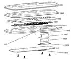
도 5는 일 실시 예에 따른 전자 장치(500)를 도시한다. 전자 장치(500)는 박막 삽입 몰딩 기술(Film Insert Moulding Technology, FIM) 부분 및 커넥터 조립체(507)를 포함한다. FIM 부분은 투명한 몰딩된 플라스틱 부분(501), 박막(502), 장식용 층(503), 터치 센서 층(504), 접지 층(512), 조명 층(505) 및 과-몰딩된 열가소성수지(506)를 포함한다. 커넥터 조립체(507)는 터치 센서 층(504)를 인쇄된 회로 기판 또는 그와 유사한 것과 같은 물리적 플랫폼을 통해 접근가능한 외부 드라이버 또는 제어기에 연결하도록 구성될 수 있고, 그것은 또한 조명 층(505) 또는 그와 유사한 것들에 전력을 공급하는 전력 인버터와 같은 다른 요소들을 수용할 수 있다.
Figure 5 illustrates an
투명한 몰딩된 플라스틱 부분(501)은 몰딩된 플라스틱 층을 포함하고, 몰딩된 플라스틱 층은 실시 예들에 따라 예를 들어, 박막(502)위로 5mm 이하의 두께를 갖도록 제공될 수 있다. 박막(502)는 폴리카보네이트(PC), 폴리에틸렌 테레프탈레이트(PET) 또는 어떤 제조 공정 내의 공정 파라미터들을 견딜 수 있는 다른 열가소성 물질을 포함하는 플라스틱 물질로 구성될 수 있고, 제조 공정들은 주입 몰딩, 열형성, 고압 형성, 액압 형성(hydroforming), 주입 몰딩 공정들을 포함한다. 공정 파라미터들은 압력, 온도 및 순환 시간을 포함할 수 있다.
The transparent molded
박막(502)는 또한 장식용 잉크 및 기능 잉크의 인쇄를 위한 기판으로서 기능하고 또는 전도성 풀, 전도성 잉크, 조명 잉크 또는 그와 유사한 것과 같이 장식용 층(503)을 형성하기 위해 사용되는 풀로서 기능한다. 장식용 층(503)은 복수의 장식용 잉크 층들로 구성된다. 기능 잉크는 박막(502)의 어느 한 면에 인쇄될 수 있다. 터치 센서 층(504)는 전도성 잉크를 사용하여 인쇄되는 전극(508) 및 트레이스(509)를 포함하여 정전식 스위치들을 형성할 수 있다.
The
접지 층(510)은 투명한 전도성 및 고립된 잉크로 인쇄되고, 잉크는 조명 층에 의해 생산된 빛의 투과율을 손상하지 않고 그럼에도 조명 층을 통전시켜 생성되는 전계를 차폐하여 간섭이 정전식 감지 구역으로 유도되는 것을 방지할 것이다.
The
조명 층(505)는 상이한 기능 층들; 투명한 전도성 잉크 층, 조명 원소 층, 은 전도성 잉크 층, 로 구성될 수 있다.
터치 센서 층(504)는 전자 장치(500)를 위한 전방 전극이다. 터치 센서 층(504)의 높은 투과율은 조명 층(505)으로부터의 빛이 시청자에게 쉽게 보일 수 있게 한다. 인쇄된 조명 층은 전기 전류가 인가될 때 빛을 방출한다.
The
열가소성수지 몰딩(506)은 FIM 부분에 구조적인 강도를 제공하는 플라스틱 층이다. 열가소성 몰딩(506)은 나오는 트레이스들(509)을 위한 구멍(511)을 갖는다. 기판은 전방 표면 및 후방 표면을 갖고, 전방 표면 또는 후방 표면은 모두 장식용 잉크 층으로 인쇄되고 설계된 그래픽을 생산하기 위해 고쳐질 수 있다. 전도성 잉크는 그래픽 층 위에 인쇄되어 정전식 감지 구역을 생산할 수 있다. 유전체 층들은 정전식 감지 구역 및 유전체 층 위에 인쇄된 발광 물질 층 위에 인쇄될 수 있다. 적절한 곳에서 다른 층들을 따라 조명 층은 광원을 생성하도록 고쳐져서 백라이팅(backlighting)을 요구하는 박막 스위치들 또는 구역의 영역들을 비출 수 있다. 기능화된 박막은 그 다음 다이 컷(die cut)되고, 고압 형성, 블로 형성(blow forming) 및 그 유사한 것들로 형성되고 주입 몰딩되어 최종 제품을 생산한다. 그 후에, 꼬리 커넥터, 지브라 커넥터, 또는 그 유사한 것과 같은 커넥터가 부착될 수 있다.
The
도 6은 일 실시 예에 따른 커넥터 조립체(600)의 분해도이다. 커넥터 조립기(600)은 커넥터(601), 케넥터 홀더(602), 인쇄 회로 기판(PCB, 604)을 갖는다. 커넥터(601)는 지브라 커넥터 또는 그와 유사한 것일 수 있다. 커넥터 홀더(602)는 한 쌍의 플레이트 구멍들(607)을 갖고, 각각의 플레이트 구멍(607)은 나사(606)을 받기 위한 것이다. 인쇄 회로 기판(604)은 4개의 PCB 구멍들(605)를 갖고, 각각의 구멍(605)은 나사(606)을 받기 위한 것이다.
6 is an exploded view of a
실시 예에서, 인쇄 동안 전도성 트레이스들이 전도성 잉크에 의해 형성된다. 이 전도성 트레이스들은 외부 접합 연결점에 연결된다. 빈 공간(511)이 커넥터(601), 지브라 커넥터와 같은,를 맞추기 위해 열가소성수지 몰딩(506) 내에 생성되어 전도성 트레이스들을 외부의 연결하는 점에 연결한다. 일련의 전도성 핑거(finger)들이 박막(502)상에 인쇄될 수 있고, 그 다음 박막(502)이 인쇄 회로 기판(604)에 연결될 수 있다. PCB는 그 다음 나사(606)에 의한 것과 같은 종래의 잠금 수단을 이용하여 FIM 부분에 잠금된다.
In an embodiment, conductive traces are formed by conductive ink during printing. These conductive traces are connected to an external joint connection point. An
도 7a는 일 실시 예에 따른 전자 장치(700)를 보여준다. 전자 장치(700)는 박막(702), 장식용 층(703), 터치 센서 층(704), 접지 층(708), 조명 층(705)를 포함하는 6개의 부분을 가져 조명 영역, 몰딩된 플라스틱(706), 외부 드라이버 또는 인쇄 회로 기판(PCB)와 같은 회로 플랫폼에 탑재된 제어기와 연결하도록 구성된 커넥터 조립체(707)를 형성하고, 전자 장치(700)는 전력 인버터 또는 그와 유사한 것이 제공될 수 있다.
7A shows an
도 7b는 일 실시 예에 따른 전자 장치(710)를 보여준다. 전자 장치(710)은 투명한 몰딩된 플라스틱 부분(701), 박막(702), 장식용 층(703), 터치 센서 층(704), 몰딩된 플라스틱(706) 및 커넥터 조립체(707)를 갖는다. 전자 장치(710)에 현저하게 없는 것은 조명 층(705)이다. 백라이팅 기능은 발광 다이오드(LEDs), 형광 발광, CCFL, 또는 그와 유사한 것과 같은 당업자에 의해 인정될 수 있는 외부 광원(미도시)을 이용하여 저낮 장치(710) 내에 여전히 제공된다.
7B shows an
도 7c는 일 실시 예에 따른 또 다른 전자 장치(720)를 보여준다. 전자 장치(720)는 투명한 몰딩된 플라스틱 부분(701), 박막(702), 장식용 층(703), 조명 층(705), 몰딩된 플라스틱(706) 및 커넥터 조립체(707)를 포함한다. 전자 장치(720)에 현저하게 없는 것은 터치 센서 층(704)이다. 대신에, 입력 기능은 기계적 스위치, 촉각 입력 장치, 또는 그와 유사한 것들의 이용을 통해 달성될 수 있다. 그러나, 실시 예들에 따라서, 조명 층(705)이 여전히 여기서 설명된 것처럼 윤곽이 만들어지고 기계적 스위치 또는 버튼을 위한 백라이팅 원천으로서 사용될 수 있다는 점이 주의될 것이다.
7C shows another
상호 연결 시스템은 양 끝단에서 케이블과 커넥터로 구성된다. 박막은 인쇄된 회로이고 이것은 “연결선(pig tail)”과 같은 회로의 연장이므로, 전도성 잉크 회로(CIC)는 가장 곧은(straight) 전달 수단이다. “연결선”의 끝은 마모 및 분자 이동에 있어 잉크 표면을 보호하기 위해 카본 잉크로 인쇄될 것을 요구할 수 있다.
The interconnect system consists of cables and connectors at both ends. The conductive ink circuit (CIC) is the straightest delivery means since the film is a printed circuit and this is an extension of the circuit, such as a " pig tail. &Quot; The ends of the " connector " may require that the carbon ink be printed to protect the ink surface in terms of wear and molecular movement.
이 방법은 정규 FIM 설계 및 역 FIM 설계 모두에 적용될 수 있다. 그러나, 설계의 유효성은 “연결선”의 유연성에 의존하며, 그것은 사용된 박막의 두께에 비례한다. “연결선”은 생산 시스템이 환경 인증 시험을 만족할 수 있도록 생산 시스템 설계에 기초하여 설계될 것을 요구한다.
This method can be applied to both regular FIM design and inverse FIM design. However, the effectiveness of the design depends on the flexibility of the "connection line", which is proportional to the thickness of the thin film used. "Connector" requires that the production system be designed based on the production system design so that it meets the environmental certification tests.
대안적으로, FFC(Flat Flexible Cable) 또는 FPC(Flexible Printed Circuit)가 박막과 보드 사이에서 다리를 놓는 데 사용될 수 있다. 박막과 FFC 또는 FPC 사이에서 다리를 놓는 커넥터들은 지브라 커넥터 또는 ACF(Anisotropic Conductive Film adhesives)일 수 있다. ACF는 두 유형들, PSA(Pressure Sensitive Adhesive) 또는 열가소성수지 접착제,를 포함할 수 있다.
Alternatively, an FFC (Flat Flexible Cable) or an FPC (Flexible Printed Circuit) can be used to bridge the foil between the foil and the board. Connectors that place the bridge between the thin film and the FFC or FPC can be zebra connectors or ACF (Anisotropic Conductive Film Adhesives). The ACF can include two types, PSA (Pressure Sensitive Adhesive) or thermoplastic adhesive.
연결선/CIC, FFC, FPC 및 PCB 사이의 연결은 PCB상에 납땜되거나 결합된 낮은 삽입력(Low Insertion Force, LIF) 또는 영 삽입력(Zeor Insertion Force, ZIF) 커넥터를 요구할 수 있다. FFC는 대안적으로 직접적으로 PCB에 납땜될 수 있다. 기계적 핀 또는 커넥터 용기는 직접적으로 CIC 및 FPC에 권축(crimp)되어 CIC 및 FPC의 끝단이 직접적으로 PCB에 납땜되거나 PCB상의 헤더로 꽂힐 수 있게 한다.
The connection between the connector / CIC, FFC, FPC and PCB may require a Low Insertion Force (LIF) or a Zeor Insertion Force (ZIF) connector soldered or mated on the PCB. The FFC can alternatively be soldered directly to the PCB. Mechanical pins or connector receptacles can be crimped directly to the CIC and FPC to allow the ends of the CIC and FPC to be directly soldered to the PCB or plugged into the header on the PCB.
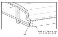
상호 연결 설계는 또한 PCB에 연결되는 단자의 위치를 포함한다. 이러한 목적에 기여할 수 있는 박막 뒤에 직접적으로 있는 세 개의 위치들이 있다. 연결의 위치 및 방법의 상세한 내용이 도 8 내지 도 39에서 보여지고, 이제 더욱 상세하게 설명될 것이다.
The interconnect design also includes the location of the terminals to be connected to the PCB. There are three positions directly behind the thin film that can contribute to this purpose. The details of the location and method of the connection are shown in Figures 8-39 and will now be described in more detail.
도 8은 전방 주입 몰딩 설계와 함께하는 “연결선”을 보여준다. 박막은 위 외표면(top appearance surface, 인쇄되지 않은 표면 또는 A 표면)상의 장식용(804) 및 기능(805) 잉크 인쇄로 형성되고 이어서 박막의 인쇄된 면(B-표면)상의 불투명한 플라스틱(806)으로 주입 몰딩된다. 도 10에서의 외부 광원(2007)이 장식용 층(804)상에 인쇄된 그래픽에 백라이트를 비출 때, 도 10의 광 차단기(1006)와 같이 이 불투명한 플라스틱(806)은 탑재하는 PCB(807)를 위한 구조로서 기여한다.
Figure 8 shows a " connection line " with a front injection molding design. The thin film is formed by decorating 804 and functional (805) ink printing on the top appearance surface (top surface, unprinted surface or A surface), and then the opaque plastic 806 ). This
“연결선(803)”은 박막 기판(802)로부터 연장된 부분이고, 그것은 전도성 트레이스들(805)로 인쇄된다. 박막의 연장된 부분은 자유 끝단이 커넥터(808), ZIF 또는 LIF 중 어느 하나,와 맞물릴 때, 인쇄된 감지 스위치 회로(805)와 PCB(807)의 연결 또는 가교로서 기여한다. 커넥터(808)는 PCB(807)상에 납땜된다. 그것은 또한 기계적으로 PCB(807)상에 탑재될 수도 있다.
The "
대안적으로, 투명한 플라스틱(905)은 박막의 인쇄 면에서 몰딩될 수 있고, 투명한 플라스틱(905) 너머의 불투명한 플라스틱인 제 2 몰딩(906)이 잇따라 올 수 있다. “연결선(902)”은 PCB(907)상에 납땜된 커넥터(908)을 통해 인쇄된 스위치 회로(904)와 PCB(907)를 가교한다. 이러한 구성은 도 9에서 보여진다.
Alternatively, the
“연결선”을 이용하는 완전한 상호 연결 시스템은 도 10에서 보여진다. 투명한 플라스틱(1002)는 인쇄된 박막 기판(1004)의 인쇄된 표면에서 주입 몰딩된다. 제 2 플라스틱 몰딩(1003)은 불투명하고 LED(1007)을 위한 광 차단기(1007)로서 기여한다.
A complete interconnect system using a " connector " is shown in FIG. The
ACF의 응용이 도 11에서 보여진다. 장식용(1103) 및 기능(1104) 잉크 층들을 구비한 형성된 박막 기판은 위 외표면(인쇄되지 않은 표면 또는 A-표면)상의 투명한 플라스틱 주입 몰딩(1101)을 갖고 이후의 박막의 인쇄된 면(B-표면)상의 불투명한 플라스틱으로 몰딩된다. 이 불투명한 플라스틱(1105)은 외부 광원(도 13에서 보여지는 1307)이 장식용 층(1103)상에 인쇄된 그래픽들을 위한 백라이팅을 제공하는 사용되고 있을 때 도 13에서의 광 차단기(1306)와 같이 탑재하는 PCB(1108)를 위한 구조로서 기여한다. 인쇄된 전도성 트레이스들(1104)은 부분적으로 테두리(1110)에 노출된다. 박막의 인쇄된 전도성 트레이스들의 노출된 부분(1111)은 단자 끝으로서 기여한다. FPC(1107) 또는 유연성 있는 케이블은 ACF(1106)을 통해 단자 끝에 부착되고, FPC 또는 유연성 있는 케이블의 다른 끝은 PCB(1108)상에 납땜된 ZIF, LIF와 같은 커넥터(1109)에 맞물릴 것이다.
The application of the ACF is shown in FIG. The formed thin film substrate with decorative 1103 and functional 1104 ink layers has a transparent
대안적으로, 투명한 플라스틱(1204)은 또한 박막의 인쇄된 측면에서 몰딩되고, 투명한 플라스티 너머의 불투명한 제 2 몰딩(1206)이 뒤따른다. 박막의 인쇄된 전도성 트레이스들(1211)의 노출된 부분(1210)은 부분의 단자 끝으로서 기여한다. 유연성 있는 인쇄 회로(FPC, 1207) 또는 유연성 있는 케이블은 한 끝에서 AFC(1206), PSA 또는 열가소성 접착제 중 어느 하나,를 통해 단자 끝에 붙는다. 다른 끝은 PCB(1208)상에 납땜된 ZIF, LIF와 같은 커넥터(1209)와 맞물린다. 이러한 구성은 도 12에서 보여진다.
Alternatively, transparent plastic 1204 is also molded on the printed side of the film followed by a transparent plastic second opaque
측면 벽상의, 외표면에 평행한(근접한) ACF를 이용한 완전한 상호 연결 시스템은 도 13 및 14에서 보여진다. 투명한 플라스틱(1302)은 인쇄된 박막 기판(1304)의 인쇄된 표면에서 주입 몰딩된다 제 2 플라스틱 몰딩(1303)은 불투명하고 광원 LED(1307)을 위한 광 차단기(1306)로서 기여한다. 도 14는 함께 조립된 FFC 또는 FPC 및 ACF의 개념을 보여준다.
A complete interconnect system using an ACF parallel (adjacent) to the outer surface of the side wall is shown in Figures 13 and 14. The
도 15는 ACF PSA 응용 및 탄성 중합체 커넥터 응용의 조합을 보여준다. 장식용(1503) 및 기능(1504) 잉크 층들을 구비한 형성된 박막 기판은 위 외표면(인쇄되지 않은 표면 또는 A-표면)상의 투명한 플라스틱 주입 몰딩(1501)을 갖고 이어서 박막의 인쇄된 면(B-표면)상의 불투명한 플라스틱(1505)으로 몰딩된다. 이 불투명한 플라스틱(1505)은 외부 광원(도 16에서 보여지는 1602)이 장식용 층 위에 인쇄된 그래픽을 백라이팅할 때 광 차단기(도 16에서 보여지는 1601)와 같이 탑재하는 PCB(1511)를 위한 구조로서 기여한다. 이 조립체에서, 인쇄된 전도성 트레이스들은 부분적으로 부분(1506)의 테두리에서 노출된다. 박막의 인쇄된 전도성 트레이스의 노출된 부분(1504)은 단자 끝으로서 기여한다. 유연성 있는 인쇄된 회로(FPC, 1508) 또는 유연성 있는 케이블은 한 끝에서 ACF를 통해 단자 끝에 부착되고, 다른 끝은 PCB(1511)상의 커넥터(1512), ZIF 또는 LIF 중 어느 하나,에 맞물린다.
15 shows a combination of an ACF PSA application and an elastomeric connector application. The formed thin film substrate with the decorative 1503 and
탄성 중합체 스페이서(elastomer spacer, 1509)는 FPC(1508) 또는 FFC의 상위에 배치된다. 이 탄성 중합체 스페이서(1509)는 PSA(1507) 등과 함께 ACF상에서 용수철 압축을 제공하여 몰딩된 부분(1504)의 단자 끝과 연결 FPC 또는 FFC(1508) 사이의 접촉을 강화한다. 탄성 중합체 스페이서(1509)는 불투명한 플라스틱 몰딩(1505)으로부터 홀더를 통해 또는 불투명한 플라스틱 몰딩(1505)에 부착된 독립적인 부분(1510)을 통해 구속될 수 있다. FPC 또는 FFC(1508)의 다른 끝은 PCB(1511)상의 납땜된 또는 달라붙은 ZIF, LIF와 같은 커넥터(1512)에 맞물린다.
An
압축 부하 상호 연결을 구비한 측면 벽상의, 외표면에 평행한(근접한) ACF를 이용한 완전한 상호 연결 시스템은 도 16에서 보여진다.
A complete interconnect system using an ACF parallel (adjacent) to the outer surface, on the side wall with a compressive load interconnect, is shown in FIG.
도 17은 ACF 응용의 또 다른 구성을 보여준다. 장식용(1703) 및 기능(1704) 잉크 층들과 함께 형성된 박막 기판은 위 외표면(인쇄되지 않은 표면 또는 A-표면)상의 투명한 플라스틱 주입 몰딩(1701)을 갖고 이어서 박막의 인쇄된 면(B-표면)상의 불투명한 플라스틱(1705)로 몰딩된다. 이 불투명한 플라스틱(1705)은 장식 층 위에 인쇄된 그래픽을 백라이팅하는 외부 광원(1802)에 대한 광 차단기(1801)와 같이 탑재하는 PCB(1708)를 위한 구조로서 기여한다. 인쇄된 전도성 트레이스들(1704)은 참조번호(1710)에서 보여지는 것처럼 장식용 층의 뒤에서 부분적으로 노출된다. 박막의 인쇄된 전도성 트레이스들의 노출된 부분(1704)은 단자 끝으로서 기여한다. 유연성 있는 인쇄된 회로(FPC, 1707) 또는 유연성 있는 케이블은 ACF(1706), PSA 또는 열가소성수지 접착제 중 어느 하나,를 통해 단자 끝에 붙고, 다른 끝은 커넥터(1709), PCB(1708)상에 납땜된 IF 또는 LIF 중 어느 하나,에 맞물린다.
Figure 17 shows another configuration of an ACF application. The thin film substrate formed with the decorative 1703 and
장식용 표면 상호 연결 뒤의 ACF를 이용한 완전한 상호 연결 시스템이 도 18에서 보여진다.
A complete interconnect system using the ACF behind the decorative surface interconnect is shown in FIG.
도 19는 ACF PSA 응용과 탄성 중합체 커넥터 응용의 조합을 보여준다. 장식용(1903) 및 기능(1904) 잉크 층과 함께 형성된 박막은 위 외표면(인쇄되지 않은 표면 또는 A-표면)상의 투명한 플라스틱 주입 몰딩(1901)을 갖고 이어서 박막의 인쇄된 면상의 불투명한 플라스틱(1905)으로 몰딩된다.
Figure 19 shows a combination of an ACF PSA application and an elastomeric connector application. The thin film formed with decorative 1903 and functional 1904 ink layers has a transparent
이 불투명한 플라스틱(1905)는 외부 광원(도 20에서 보여지는 2002)이 장식 층 내의 인쇄된 그래픽들을 백라이팅할 때 도 20의 광 차단기(2001)와 같이 탑재하는 PCB(1910)를 위한 구조로서 기여한다. 인쇄된 전도성 트레이스들(1913)은 장식용 층의 뒤에서 구멍(1912)과 함께 노출된다. 박막의 인쇄된 전도성 트레이스의 노출된 부분(1913)은 단자 끝으로서 기여한다. 유연성 있는 인쇄된 회로(FPC, 1907) 또는 유연성 있는 케이블은 ACF PSA(1906)을 통해 단자 끝에 부착되고, 다른 끝은 PCB(1910)상의 커넥터(1911), ZIF 또는 LIF 중 어느 하나,에 맞물린다.
This opaque plastic 1905 contributes as a structure for the
탄성 중합체 스페이서(1908)은 FPC(1907) 또는 FFC의 상위에 배치된다. 이 탄성 중합체 스페이서(1908)는 PSA(1906) 위 등에 용수철 압력을 제공하여, 단자 트레이스와 연결 FPC(1907) 또는 FFC 사이의 접촉을 강화시킨다. 탄성 중합체 스페이서(1908)는 불투명한 플라스팅 몰딩(1905) 상의 홀더 또는 불투명한 플라스틱 몰딩(1905)에 부착된 독립적인 부분(1909)을 통해 구속될 수 있다. FPC(1907) 또는 FFC의 다른 끝은 PCB(1910)상에 납땜된 또는 붙은 ZIF, LIF와 같은 커넥터(1911)에 맞물린다.
The
상호 연결을 잠그는 탄성 중합체를 구비한 장식용 표면 뒤의 ACF를 이용하는 완전한 상호 연결 시스템은 도 20 및 21에서 보여진다.
A complete interconnect system using an ACF behind the ornamental surface with an elastomeric locking interconnect is shown in Figures 20 and 21.
도 22는 ACF 응용의 또 다른 구성을 보여준다. 장식용(2203) 및 기능(2204) 잉크 층과 함께 형성된 박막 기판은 위 외표면(인쇄되지 않은 표면 또는 A-표면)상의 투명한 플라스틱 주입 몰딩(2201)을 갖고, 이어서 박막의 인쇄된 면상의 불투명한 플라스틱(2205)으로 몰딩된다. 이 불투명한 플라스틱(2205)은 외부 광원(도 24에서 2402)이 장식용 층(2203)상에 인쇄된 그래픽을 백라이팅할 때 광 차단기(도 24에서 2401)와 같이 탑재하는 PCB(2209)를 위한 구조로서 기여한다. 이 조합체이서, 회로 트레이스들(2204)은 측면 벽(2206)에서 부분적으로 노출된다. 박막의 인쇄된 전도성 트레이스들(2204)의 노출된 부분은 부분의 단자 끝으로서 기여한다. 유연성 있는 인쇄된 회로(2208) 또는 유연성 있는 케이블은 ACF(2207), PSA 또는 열가소성수지 접착제 중 어느 하나,를 통해 단자 끝에 붙는다; 다른 끝은 PCB(2209)상에서 커넥터(2210), ZIF 또는 LIF 중 어느 하나,와 맞물린다.
22 shows another configuration of the ACF application. The thin film substrate formed with the decorative 2203 and functional 2204 ink layers has a transparent
박막의 외표면 상의 투명한 플라스틱(2304)은 또한 박막의 인쇄된 면에서 몰딩되고 불투명한 플라스틱(2306)인 제 2 몰딩이 뒤따를 수 있다. 박막의 인쇄된 전도성 트레이스의 노출된 부분(2303)은 부분의 단자 끝으로서 기여한다. 유연성 있는 인쇄된 회로(2308) 또는 유연성 있는 케이블은 ACF, PSA 또는 열가소성수지 접착제 중 어느 하나,를 통해서 단자 끝에 붙는다; 다른 끝은 PCB(2309)상의 커넥터, ZIF 또는 LIF 또는 그와 유사한 것,에 맞물린다. 이러한 구성은 도 23에서 보여진다.
The transparent plastic 2304 on the outer surface of the film may also be followed by a second molding that is molded on the printed side of the film and is opaque plastic 2306. The exposed
측면 벽상의, 외표면 상호 연결에 수평인(근접한), ACF를 이용한 완전한 상호 연결 시스템은 도 24 및 25에서 보여진다.
A complete interconnect system using the ACF, horizontal (close) to the lateral wall, outer surface interconnections, is shown in FIGS. 24 and 25.
도 26은 탄성 중합체 커넥터 응용의 예를 보여준다. 장식용(2603) 및 기능(2604) 잉크 층들과 함께 형성된 박막은 위 외표면(인쇄되지 않은 표면 또는 A-표면)상의 투명한 플라스틱 주입 몰딩(2601)을 갖고, 이어서 박막의 인쇄된 면(B-표면)상의 불투명한 플라스틱으로 몰딩된다. 불투명한 플라스틱은 장식용 층 위의 인쇄된 그래픽에 백라이팅하는 외부 광원(도 27에서 2702)을 위한 광 차단기(도 27에서 2701)과 같이 탑재하는 PCB(2607)을 위한 구조로서 기여한다. 인쇄된 전도성 트레이스들은 장식용 층의 뒤에서 부분적으로 노출(2608)된다. 박막의 인쇄된 전도성 트레이스의 노출된 부분(2609)은 단자 끝으로서 기여한다. 탄성 중합체 커넥터(2606), 지브라 커넥터와 같은,는 인쇄된 전도성 트레이스들(2609)를 PCB(2607) 트레이스들에 연결한다. 탄성 중합체 커넥터(2606)은 불투명한 플라스틱 몰딩(2605)상의 홀더를 통해 구속될 수 있고 또는, 도 26에서 보여지는 것처럼 독립적인 홀더가 불투명한 플라스틱 몰딩(2605)에 부착된다.
Figure 26 shows an example of an elastomeric connector application. The thin film formed with decorative 2603 and functional 2604 ink layers has a transparent
지브라 커넥터(2606)은 마주보는 미러-이미지(mirror-image) 패드 패턴들 사이에서 구부러질 때, 유연한 표면-대-표면(surface-to-surface) 압축 컨넥터를 제공하는 납땜을 요구하지 않는 영 삽입력 커넥터이다. 탄성 중합체 커넥터들은 전도성 및 비전도성 실리콘 고무의 교차하는 층들로 구성된다. 실리콘 고무는 훌륭한 노화 속성, 화학적 안정성, 전기적 신뢰성 및 충격과 진동에 있어서 우수한 성능을 갖기 때문에, 기초 물질이 된다. 그것은 또한 접촉 표면들을 보호하는 개스킷(gasket)과 유사한 봉인을 제공한다.
The
전도성 층들은 실리콘 고무 내에서 분산되는 작은 전도성 입자들로 구성된다. 전도성 층들 각각의 안에서, 전도성 입자들은 수천의 전도성 경로를 만들어낸다. 그러므로, 각각의 전도성 층은 기판 인터페이스에서 다중 접촉점들을 제공한다. 전도성 층들이 접합 패드들 사이의 접촉을 보장하는 동안, 비전도성 층들은 전도성 층들을 서로로부터 격리시킨다. 이러한 수천의 전도성 경로로들과 연결된 다중 층들은 신뢰할 수 있는 전기적 연결을 보장한다.
The conductive layers consist of small conductive particles dispersed in the silicone rubber. Within each of the conductive layers, the conductive particles create thousands of conductive paths. Therefore, each conductive layer provides multiple contact points at the substrate interface. While the conductive layers ensure contact between the bonding pads, the nonconductive layers isolate the conductive layers from each other. Multiple layers connected to these thousands of conductive pathways ensure reliable electrical connections.
장식용 표면 상호 연결 뒤의 탄성 중합체를 이용한 완전한 상호 연결 시스템은 도 27에서 보여진다.
A complete interconnect system using an elastomer after decorative surface interconnections is shown in FIG.
이러한 방법은 상호 연결을 위한 적절한 구역을 위치시키기 위한 많은 선택권을 제공한다. 그것은 연결 구역 상에서 더 나은 기계적 스트레스 제어를 갖는다. 조임력(clamping force)은 나사에 의해 제어된다.
This method provides many options for locating the appropriate zones for interconnections. It has better mechanical stress control over the connection area. The clamping force is controlled by a screw.
탄성 중합체 커넥터의 또 다른 응용이 도 28에서 보여진다. 장식용(2803) 및 기능(2804) 잉크 층들로 형성된 박막 기판은 위 외표면(인쇄되지 않은 표면 또는 A-표면)상의 투명한 플라스틱 주입 몰딩(2801)을 갖고 이어서 박막의 인쇄된 면(B-표면)상의 불투명한 플라스틱(2805)으로 몰딩된다. 이 불투명한 플라스틱(2805)는 외부 광원(2902)이 장식용 층 위에 인쇄된 그래픽을 백라이팅할 때 광 차단기(2901)과 같이 탑재하는 PCB(2802)를 위한 구조로서 기여한다. 회로 인쇄된 전도성 트레이스들(2804)은 테두리 부분(2809)에서 부분적으로 노출된다. 박막의 인쇄된 전도성 트레이스들의 노출된 부분 단자 끝으로서 기여한다. 탄성 중합체 커넥터(2806), 지브라 커넥터와 같은,는 인쇄 전도성 트레이스들(2804)를 PCB(2808) 트레이스들에 직접적으로 연결하는 데 사용될 것이다. 탄성 중합체 커넥터(2806)은 또한 불투명한 플라스틱 몰딩(2805)상의 홀더 또는 불투명한 플라스틱 몰딩(2805)에 부착된 독립적인 홀더(2807)를 통해 구속될 수 있다.
Another application of an elastomeric connector is shown in Fig. The thin film substrate formed from decorative 2803 and functional 2804 ink layers has a transparent
측면 벽상의, 외표면 상호 연결에 평행한(근접한), 탄성 중합체 커넥터를 이용한 완전한 상호 연결 시스템은 도 29에서 보여진다.
A complete interconnect system using elastomeric connectors parallel to (adjacent to) the lateral wall, outer surface interconnections is shown in FIG.
이러한 방법은 상호 연결을 위한 적절한 구역을 위치시키는 많은 선택권을 제공한다. 그것은 연결 구역 상에서 더 좋은 기계적 스트레스 제어를 갖는다. 조임력은 나사에 의해 제어된다.
This method provides many options for locating the appropriate zone for the interconnect. It has better mechanical stress control over the connection area. The tightening force is controlled by screws.
촉각 피드백은 장치를 통해 사용자에게 힘, 진동 및/또는 움직임을 적용함으로써 우리의 터치 감각을 이용한다.Tactile feedback utilizes our touch sense by applying force, vibration, and / or motion to the user through the device.
- 터치는 우리가 태어날 때 발달하는 최초의 감각이고 죽기 전에 사용되는 최후의 감각이다.- Touch is the first sensation that develops when we are born and the last sensation used before death.
- 그것은 시각보다 20배 더 빠르다.- It is 20 times faster than visual.
- 장치와의 지속적인 사용자 상호 작용이 필요하지 않다.- No ongoing user interaction with the device is required.
- 인간은 1000 헤르츠(Hz)까지 진동에 매우 민감하다(250 헤르츠에서 가장 민감함)- Humans are very sensitive to vibrations up to 1000 hertz (Hz) (most sensitive at 250 hertz)
- 사용자는 모바일 장치보다 더 주변의 실제 환경 및 사람들과 상호 작용할 수 있다.
- The user can interact with the physical environment and people around him more than the mobile device.
촉각 피드백은 변화하는 빈도 및 민감도를 갖는 진동 알람(alarm)을 이용한 효과적인 통신 모드로서 사용될 수 있다. 촉각은 자기수용성 감각 및 촉각성 감각 모두를 포함하고, 다른 감각들과 협력하여, 또는 전자 응용들과의 상호 작용에 터치(촉각성) 감각 및 제어를 적용하는 과학적 수단을 포함한다.
Haptic feedback can be used as an effective communication mode using a vibration alarm with varying frequency and sensitivity. Tactile sense includes both self-accepting and tactile sensations, and includes scientific means of applying touch (tactile) sensations and control in cooperation with other senses, or in interaction with electronic applications.
촉각 기술 스펙트럼(spectrum)은 다음을 포함할 수 있다.The tactile technique spectrum may include the following:
- 질량/무게- Weight / Weight
- 단단함/디텐트(detent)- Hardness / detent
- 점성/감쇠- viscosity / attenuation
- 거침/질감- rough texture
- 펄스(맥박)- Pulse (pulse)
- 파형- Waveform
- 진동- vibration
- 동시적 합성 효과
- Simultaneous synthesis effect
전자 장치의 표면은 인쇄된 박막으로부터 특정한 미리 결정된 기능을 나타내는 다양한 윤곽들로 설계될 수 있다. 둥근 오목 영역의 단일 터치는 박막상의 터치 패드를 작동시킬 것이고, 특정한 신호가 상호 작용을 통해 제어기로 보내질 것이다. 회전 구역의 오목한 부분은 사용자의 손가락을 회전 구역 아래에 위치한 터치 패드 주변으로 안내한다. 유사하게, 미끄러짐 구역을 위한 오목한 구역은 손가락이 미끄러짐을 따라 움직이도록 안내하여 제어 파라미터들을 변화시킨다. 사용자는 표면의 윤곽을 느끼고, 동시에 사용자는 표면상에서 거침/촉감 또는 특정하게 설계된 돌출부를 느낄 수 있어 터치 구역의 특정한 기능을 인식할 수 있다. 멈춤(detention)이 터치 패드 위치의 더 나은 인식을 제공하기 위해 표면에 추가될 수 있다. 도 30은 손가락이 표면을 터치할 때의 멈춤 및 마찰 촉각 피드백을 보여준다.
The surface of the electronic device may be designed with various contours representing a specific predetermined function from the printed thin film. A single touch in the round recessed area will activate the thin touchpad, and a specific signal will be sent to the controller through interaction. The concave portion of the rotation zone guides the user's finger around the touch pad located below the rotation zone. Similarly, the recessed area for the slip area guides the finger to move along the slip to change the control parameters. The user can feel the contour of the surface while at the same time the user can feel a rough / tactile or specially designed protrusion on the surface, thus recognizing the specific function of the touch zone. Detents can be added to the surface to provide better recognition of the touchpad location. 30 shows the stop and friction tactile feedback when the finger touches the surface.
불투명한 플라스틱 몰딩의 뒤에 버저(buzzer)를 탑재함으로써 오디오 장치가 시스템에 추가될 수 있다. 버저는 손가락이 터치 패드가 위치한 구역에서 표면을 터치할 때 활성화될 것이다.
An audio device can be added to the system by mounting a buzzer behind the opaque plastic molding. The buzzer will be activated when the finger touches the surface in the area where the touchpad is located.
손가락이 터치 패드 표면을 터치하거나 그에 근접할 때, 마이크로컨트롤러(microcontroller)는 PWM 신호를 생성하여 사용자에 대해 들을 수 있는 피드백을 생산하도록 버저를 구동한다. 들을 수 있는 소리는 음악, 노래 또는 사용자를 경고하는 다른 경고 소리로 미리 프로그램될 수 있다. 소리는 손가락이 감지 구역으로부터 벗어날 때 자동적으로 꺼진다.
When the finger touches or approaches the touchpad surface, the microcontroller generates a PWM signal to drive the buzzer to produce audible feedback to the user. The audible sounds can be pre-programmed with music, songs or other warning sounds to warn the user. The sound is automatically turned off when the finger leaves the sensing area.
유사하게, 다른 촉각 장치들, 진동기와 같은,이 불투명한 플라스틱 몰딩의 뒤에 탑재될 수 있다. 진동으로부터의 펄스는 터치 패드들이 인쇄되어 사용자에 대한 추가 피드백이 달성될 수 있는 전자 장치의 표면을 터치하거나 미끄러질 때 손가락 끝에서 느껴질 수 있다. 진동기는 자루(shaft)에 탑재된 불균형한 균형추(counter weight)를 구비한 DC 전동기일 수 있다. 터치 패드가 위치될 때 손가락이 장치의 표면을 터치할 때, 마이크로컨트롤러는 전동기를 켜고, 손가락이 터치 패드를 떠날 때 전동기는 자동적으로 꺼질 것이다.
Similarly, other haptic devices, such as a vibrator, can be mounted behind this opaque plastic molding. The pulses from the vibrations may be felt at the fingertip as the touch pads are printed and when touching or sliding the surface of the electronic device where additional feedback to the user can be achieved. The vibrator may be a DC motor with an unbalanced counterweight mounted on a shaft. When the finger touches the surface of the device when the touchpad is positioned, the microcontroller turns on the motor and the motor automatically turns off when the finger leaves the touchpad.
도 31은 터치 센서, 조명 또는 양쪽 모두와 같은 전자 장치를 생산하는 FIM 공정을 도시한다. 그것은 도한 형성과 몰딩에 있어서 상이한 구성들을 도시한다.
31 illustrates an FIM process for producing an electronic device such as a touch sensor, an illumination, or both. It shows different configurations for forming and molding.
3110에서, 박막 기판은 통(roll) 형태로부터 크기를 맞추기 위해 잘려진다. 박막 기판은 폴리카보네이트 또는 PET일 수 있다. 박막 두께는 0.175부터 0.5 밀리미터(mm)까지 달라진다. 박막 기판의 표면 마감질(finish)은 광택-광택(glossy-glossy), 광택-무광(glossy-matt), 무광-무광(matt-matt) 및 다른 특별한 질감, 부싱선(bushed line)과 같은,을 포함한다.
At 3110, the thin film substrate is cut to size from a roll shape. The thin film substrate may be polycarbonate or PET. Thickness varies from 0.175 to 0.5 millimeters (mm). The surface finish of the thin film substrate may be selected from the group consisting of glossy-glossy, glossy-matt, matt-matt and other special textures, such as bushed lines, .
3120에서, 장식용(그래픽) 잉크 층이 박막 기판의 B-표면상에 인쇄된다. 장식용 잉크들은 고압 열적 형성을 위해 특별하게 만들어지는 한편, 씻겨짐 없이 열가소성수지 주입 몰딩을 견뎌낼 수 있다.
At 3120, a decorative (graphical) ink layer is printed on the B-surface of the thin film substrate. The decorative inks are specially made for high pressure thermal forming, but can withstand the thermoplastic injection molding without being washed away.
3131 내지 3133에서, 전기 또는 기능 층은 터치 센서(3131), 조명(3132) 또는 터치 센서와 조명의 조합(3133)을 포함할 수 있다. 3131에서, 터치 센서 기능 층은 전기적으로 전도성인 잉크/풀을 이용하여 인쇄되어, 반투명 및 불투명함을 포함한다. 터치 센서 기능 층은 트레이스들 및 전극들로 구성된다. 트레이스 폭은 생산 설계 및 다른 트레이스 파라미터들에 따라 굽거나 늘어나는 구역에서 0.2 밀리미터(mm)보다 작거나 0.3 밀리미터(mm)보다 클 수 있고, 그것은 균열의 변화를 최소화할 수 있다. 트레이스 및/또는 전극은 은 풀 등:EA-510, 진보 전자 물질 주식회사(Advance Electronic Material Inc.)에 의해 제조되는,일 수 있다. 트레이스를 두껍게(넓게가 아님) 하기 위해서, 동일한 트레이스가 둘 이상의 층에 인쇄될 수 있다. 큐어링(curing) 공정은 이후의 새로운 층을 인쇄하기 전에 완료할 필요가 있다. 각 층의 두께는 8 내지 14 마이크로미터(μm)까지 달라진다.
In 3131 through 3133, the electrical or functional layer may comprise a
3132에서, 조명 층이 인쇄된다; 예를 들어 만일 EL이 광원으로서 사용되는 경우, 인쇄는 반투명한 전도성 물질(401), 인광체(402), 유전체(403) 및 전도성 전극(404)을 포함한다.
At 3132, an illumination layer is printed; For example, if the EL is used as a light source, printing includes a translucent
3133에서, 터치 센서 및 조명은 조명 층에 의해 생성된 간섭을 차단하기 위해 사이에서 접지 층을 필요로 한다; 그렇지 않으면, 터치 센서는 기능할 수 없을 것이다. 접지 층은 투명한 프라이머 및 전도성 트레이스(반투명한 또는 불투명한)로 구성된다. 투명한 프라이머는 전도성 트레이스가 마모 및 산화되는 것을 방지하는 것처럼 균열로부터 보호한다. 프라이머는 장식용 잉크의 동일한 족(family) 및 동일한 제조자일 수 있다. 프라이머는 절연하고, 빛의 전송이 가능하게 하고, 두 개의 호환되지 않는 층들을 접착하고, 전도성 트레이스를 마모 및 부식으로부터 보호하고, 인쇄 층과 몰딩 층을 접착한다.
At 3133, the touch sensor and illumination require a ground layer between them to block the interference generated by the illumination layer; Otherwise, the touch sensor will not be able to function. The ground layer consists of a transparent primer and a conductive trace (translucent or opaque). The transparent primer protects the conductive traces from cracking as well as preventing wear and oxidation. The primers may be the same family of decorative inks and the same manufacturer. The primers insulate, enable light transmission, adhere the two incompatible layers, protect the conductive traces from wear and corrosion, and bond the print layer and the molding layer.
3140에서, 기능 층을 인쇄하고 고친 후에, 프라이머의 하나 내지 두 개 층들이 상부에서 인쇄된다. 프라이머는 기능 층에 보호를 제공하고, 기능 층과 열가소성수지 몰딩 인터페이스(interface) 사이의 강한 접착력을 가능하게 할 수 있다.
At 3140, after printing and fixing the functional layer, one or two layers of primer are printed on top. The primer can provide protection to the functional layer and enable strong adhesion between the functional layer and the thermoplastic molding interface.
3151에서, 정규 형태화 또는 형성은 형성 도구와 접촉하는 인쇄된 표면 또는 B-표면 및 고압 공기에 노출된 박막 기판의 다른 면을 구비한 인쇄된 박막 기판을 만든다. 박막 기판은 원하는 형태 또는 윤곽을 만들기 위해 형성될 것이다. A-표면에서 트레이스 회로망 인쇄 표시 드러냄을 최소화하기 위해, 0.25 밀리미터(mm) 이상의 두께를 갖는 광택-무광 박막 기판이 사용될 수 있다.
At 3151, normal shaping or forming produces a printed thin film substrate having a printed surface or B-surface in contact with the forming tool and the other side of the thin film substrate exposed to high pressure air. The thin film substrate will be formed to produce the desired shape or contour. To minimize the exposure of the trace network print marks on the A-surface, a glossy-matte thin film substrate having a thickness of 0.25 millimeters (mm) or more can be used.
3152에서, 역 형태화 또는 역 형성은 정규 형성과 반대이고, 그래서 인쇄된 박막 기판은 형성 도구와 접촉하는 인쇄되지 않은 표면 또는 A-표면 및 고압 공기에 노출된 박막 기판의 다른 면으로 형성된다. 박막 기판은 원하는 형태 또는 윤곽을 만들기 위해 형성될 것이다. 이러한 형성 방법에 있어서, 박막 기판의 두께는 0.25 밀리미터(mm) 이상이다.
At 3152, the inverse shaping or inverse is opposite to normal formation, so that the printed thin film substrate is formed of an unprinted surface or A-surface in contact with the forming tool and the other side of the thin film substrate exposed to high pressure air. The thin film substrate will be formed to produce the desired shape or contour. In this forming method, the thickness of the thin film substrate is 0.25 millimeters (mm) or more.
0.3 밀리미터(mm)의 트레이스 폭을 갖는 단일 층 전도성 트레이스에 있어서; 어떤 윤곽화된 감지 영역의 구부러짐 반경(bending radius)은 박막 기판 두께의 두 배일 수 잇다. 0.3 밀리미터(mm)의 트레이스 폭을 갖는 두 배 층 전도성 트레이스에 있어서; 구부러짐 반경은 약간 감소될 수 있다. 더욱 빽빽한 기하학적 구조에 대해서, 더 두꺼운 트레이스들 또는 더 많은 트레이스 층들이 요구될 수 있다.
1. A single layer conductive trace having a trace width of 0.3 millimeters (mm); The bending radius of any contoured sensing area can be twice the thickness of the thin film substrate. For double layer conductive traces having a trace width of 0.3 millimeters (mm); The bending radius can be slightly reduced. For thicker geometries, thicker traces or more trace layers may be required.
3160에서, 형성된 박막 기판은 주입 몰드 빈 공간 내에 탑재되기 위해 원하는 크기로 단수화(singulate)되거나 잘려진다. 3170에서, 단수화된 형성된 박막은 열가소성 몰딩 공정을 위해 주입 몰드 내에 삽입된다.
At 3160, the formed thin film substrate is singulated or cut to the desired size to be loaded into the injection mold cavity space. At 3170, the monolith formed thin film is inserted into the injection mold for the thermoplastic molding process.
3181에서, 정규 FIM 또는 과몰딩(overmoulding)은 역 형성 박막 기판(3152)를 이용함으로써, A-표면상의 불편한 인쇄 표시들을 최소화한다. 열가소성수지 물질은 박막 기판의 B-표면을 채우기 위해 몰드 내로 주입된다. 전형적으로, 이 단계를 위한 열가소성수지 물질은 투명/반투명한 열적 플라스틱 물질이다; 두께는 1 밀리미터(mm) 이상이다. 장식용 잉크가 “씻겨 나가는 것(wash-off)”을 피하기 위해, 주입 몰드의 자리잡기(locating)에 대한 게이팅(gating)은 적절하게 선택되어야 하고/또는 장식용 잉크는 충분하게 큐어링(curing)되어야 한다.
At 3181, normal FIM or overmoulding minimizes uncomfortable print marks on the A-surface by using the reverse forming
3182에서, 역 FIM 또는 과몰딩은 박막의 A-표면을 채우기 위해 열가소성수지 물질을 몰드 내로 주입한다. 전형적으로, 이 단계를 위한 열가소성수지 물질은 투명/반투명한 열적 플라스틱 물질이다; 두께는 3 밀리미터(mm) 이하이다.
At 3182, the inverse FIM or overmolding injects the thermoplastic resin material into the mold to fill the A-surface of the film. Typically, the thermoplastic resin material for this step is a transparent / translucent thermoplastic material; The thickness is 3 millimeters (mm) or less.
3191에서, 제 2 열가소성수지 몰딩이 제 1 몰딩 층 위로 주입된다. 전형적으로 제 2 몰딩은 불투명하다. 불투명한 플라스틱으로 몰딩되지 않은 선택적인 구역은 빛이 LED로부터 터치 활성화 점 또는 조명 피드백을 위한 백라이팅으로서 통과할 수 있게 한다.
At 3191, a second thermoplastic molding is injected over the first molding layer. Typically, the second molding is opaque. An optional zone that is not molded with opaque plastic allows light to pass from the LED as a touch activation point or backlighting for illumination feedback.
3192에서, 열가소성수지는 3139과 유사하게, B-표면상에 주입된다. 제 2 몰딩은 불투명하지만 몰딩은 투명한 몰딩의 반대 면에 있다. 불투명한 플라스틱으로 몰딩되지 않은 선택적인 구역은 빛이 LED로부터 터치 활성화 점 또는 조명 피드백을 위한 백라이팅으로서 통과할 수 있게 한다.
In 3192, the thermoplastic resin is injected onto the B-surface, similar to 3139. The second molding is opaque, but the molding is on the opposite side of the transparent molding. An optional zone that is not molded with opaque plastic allows light to pass from the LED as a touch activation point or backlighting for illumination feedback.
3193에서, FIM 부분은 완성된다. 상이한 필요 조건 또는 응용에 따라; 3191, 3181, 3192 또는 3182가 전자 장치의 최종 단계가 될 수 있다. 3194에서, 커넥터는 전자 장치에 부착되고 PCB에 연결된다.
At 3193, the FIM part is completed. Depending on different requirements or applications; 3191, 3181, 3192 or 3182 may be the final stage of the electronic device. In 3194, a connector is attached to an electronic device and connected to a PCB.
본 발명과 관계된 예시적인 실시 예가 설명되고 도시되어 왔음에도 불구하고, 본 청구범위로부터 벗어남이 없이 특정한 설계, 구현 또는 구성과 관련된 많은 변형 또는 변경이 가능하고 만들어질 수 있음이 관련된 기술 분야의 당업자에 의해 이해될 것이다.It should be understood by those skilled in the relevant art that many variations or modifications can be made and made with respect to a particular design, implementation, or configuration without departing from the scope of the present invention, .
Claims (22)
Translated fromKorean상기 패턴이 형성된 기판을 3차원 윤곽으로 형태화하는 단계로서, 상기 윤곽은 상기 전기층의 하나 이상의 감지 구역에 있거나 인접한 부분에서 경사도가 변화하는, 상기 형태화하는 단계; 및
상기 형태화된 기판을 과-몰딩하는 단계를 포함하되,
상기 형태화 또는 상기 과-몰딩 동안 상기 하나 이상의 감지 구역에 있거나 인접한 상기 전기층 내의 트레이스(trace)의 저하(degradation)는,
상기 트레이스의 폭,
상기 트레이스의 층들의 수 또는 두께,
상기 트레이스의 구부러짐 반경, 및
상기 트레이스 상의 층 위의 프라이머(primer) 중 하나 이상에 기초하여 감소되며,
상기 폭은 0.2 밀리미터보다 크고 상기 전기층의 폭보다는 작고,
상기 트레이스의 물질은 전도성(conductive) 및 연성이 있고 상기 기판에 대해 강한 접착력을 갖는 은 풀(silver paste) 또는 은 잉크(silver ink)인 것을 특징으로 하는, 몰딩 방법.
Patterning one or more electrical layers on the substrate;
Shaping the patterned substrate into a three dimensional contour, wherein the contour is in the at least one sensing zone of the electrical layer or the gradient varies in the adjacent portion; And
Over-molding the shaped substrate,
The degradation of the trace in the electrical layer in or adjacent to the one or more sensing zones during the shaping or over-
The width of the trace,
The number or thickness of the layers of the trace,
The bending radius of the trace, and
Based on at least one of the primers on the layer on the trace,
The width being greater than 0.2 millimeter and less than the width of the electrical layer,
Wherein the material of the trace is silver paste or silver ink having conductivity and ductility and having a strong adhesion to the substrate.
상기 층들의 수는 2개 또는 3개인 것을 특징으로 하는, 몰딩 방법.
The method according to claim 1,
Wherein the number of layers is two or three.
상기 구부러짐 반경은 적어도 상기 기판 두께의 두 배인 것을 특징으로 하는, 몰딩 방법.
The method according to claim 1,
Wherein the bending radius is at least twice the substrate thickness.
상기 층위의 프라이머는,
상기 전기층들 중 제 1 전기층 위에 있는, 제 1 투명한 프라이머 층;
상기 제 1 투명한 프라이머 층 위에 있는, 상기 전기층들 중 제 2 전기층; 및
상기 제 2 전기층 위에 있는, 제 2 투명한 프라이머 층을 포함하는 것을 특징으로 하는, 몰딩 방법.
The method according to claim 1,
The primer of the above-
A first transparent primer layer over the first of the electrical layers;
A second one of the electrical layers above the first transparent primer layer; And
And a second transparent primer layer overlying the second electrical layer.
상기 제 2 투명한 프라이머 층 위에 있는, 상기 전기층들 중 제 3 전기층을 패턴하는 단계를 더 포함하되,
상기 제 1 , 제 2 및 제 3 전기층들은 상이한 전기적(electrical) 기능들을 갖도록 구성되고, 제 1 전기층은 적어도 부분적으로 투명한 것인 것을 특징으로 하는, 몰딩 방법.
The method according to claim 6,
Patterning a third of the electrical layers above the second transparent primer layer,
Wherein the first, second and third electrical layers are configured to have different electrical functions, and wherein the first electrical layer is at least partially transparent.
상기 제 2 전기층은 접지된 차폐 층이고, 상기 제 3 전기층은 전기발광(electroluminescent, EL) 층, 교류 전기발광(ACEL) 층, 직류 전기발광(DCEL) 층 또는 유기 LED(OLDE) 층인 것을 특징으로 하는, 몰딩 방법.
8. The method of claim 7,
The second electrical layer is a grounded shield layer and the third electrical layer is an electroluminescent (EL) layer, an alternating current electroluminescent (ACEL) layer, a direct current electroluminescent (DCEL) layer or an organic LED Molding method.
상기 기판의 두께는 0.175 밀리미터와 0.5 밀리미터 사이인 것을 특징으로 하는, 몰딩 방법.
The method according to claim 1,
Wherein the thickness of the substrate is between 0.175 millimeters and 0.5 millimeters.
상기 형태화하는 단계는 정규 구성 또는 역 구성으로 고압 열 형성하는 단계인 것을 특징으로 하는, 몰딩 방법.
The method according to claim 1,
Wherein the shaping step is a step of forming a high-pressure column in a normal configuration or a reverse configuration.
상기 과-몰딩하는 단계는 정규 구성 또는 역 구성으로 박막 삽입 몰딩하는 단계이고, 0.8 밀리미터에서 5밀리미터 사이의 두께를 갖는 열가소성수지 층을 주입 몰딩하는 단계를 포함하는 것을 특징으로 하는, 몰딩 방법.
The method according to claim 1,
The overmolding step is a step of thin-film insert molding in a normal configuration or a reverse configuration, and comprises injection molding a thermoplastic resin layer having a thickness between 0.8 mm and 5 mm.
상기 과-몰딩된 기판은 터치 또는 근접 센서를 포함하는 전자적 인터페이스장치인 것을 특징으로 하는, 몰딩 방법.
The method according to claim 1,
Wherein the over-molded substrate is an electronic interface device comprising a touch or proximity sensor.
상기 터치 또는 근접 센서는 소정의 그룹으로부터 선택되는 촉각 피드백 기능을 포함하고,
상기 소정의 그룹은 감지 구역의 조명, 센서의 임계 질량 또는 무게, 단단함 또는 디텐트(detent), 점성 또는 감쇠, 감지 구역의 거침 또는 질감, 펄스, 파형, 진동 및 그것들의 어떤 조합을 포함하는 것을 특징으로 하는, 몰딩 방법.
13. The method of claim 12,
Wherein the touch or proximity sensor comprises a tactile feedback function selected from a predetermined group,
The predetermined group may include any combination of illumination of the sensing zone, critical mass or weight of the sensor, rigidity or detent, viscosity or attenuation, roughness or texture of the sensing zone, pulse, waveform, Molding method.
상기 전기층들로부터 제어기까지의 상호 연결을 형성하는 단계를 더 포함하되,
상기 상호 연결은:
전도성 잉크 회로 또는 연결선,
외표면에 평행하거나 근접하여, 측면 벽상에 달라붙은 이방성(anisotropic) 전도성 박막,
압축 부하와 함께 외표면에 평행하거나 근접하여, 측면 벽상에 달라붙은 이방성 전도성 박막,
장식용 표면 뒤에 달라붙은 이방성 전도성 박막,
탄성 중합체(elastomeric) 잠금부를 구비한 장식용 표면의 뒤에 달라붙은 이방성 전도성 박막,
외표면에 수직하거나 근접하여, 측면 벽상에 달라붙은 이방성 전도성 박막,
장식용 표면의 뒤의 탄성 중합체 커넥터, 및
외표면에 평행하거나 근접한, 측면 벽상의 탄성 중합체 커넥터로 구성된 그룹으로부터 선택되는 것을 특징으로 하는, 몰딩 방법.
The method according to claim 1,
Further comprising forming interconnections from the electrical layers to the controller,
The interconnection is:
Conductive ink circuit or connection line,
Anisotropic conductive thin films which are parallel or close to the outer surface and stick to the side walls,
Anisotropically conductive thin films adhered to the side walls in parallel or close to the outer surface together with the compressive load,
Anisotropic conductive thin film sticking behind decorative surface,
An anisotropic conductive film sticking to the back of the decorative surface with an elastomeric locking portion,
Anisotropically conductive thin films adhered on the side walls perpendicularly or in close proximity to the outer surface,
An elastomeric connector behind the decorative surface, and
Wherein the elastomeric connector is selected from the group consisting of an elastomeric connector on the side wall that is parallel or near the outer surface.
상기 형태화된 기판상의 과-몰딩 부분을 포함하되,
상기 전기층은 상기 하나 이상의 감지 구역에 있거나 인접한 트레이스(trace)를 포함하고,
상기 전기층 내의 상기 트레이스의 저하(degradation)는,
상기 트레이스의 폭,
상기 트레이스의 두께 또는 층들의 수,
상기 트레이스의 구부러짐 반경, 및
상기 트레이스 상의 층 위의 프라이머(primer) 중 하나 이상에 기초하여 감소되며,
상기 폭은 0.2 밀리미터보다 크고 상기 전기층의 폭보다는 작고,
상기 트레이스의 물질은 전도성(conductive) 및 연성이 있고 상기 기판에 대해 강한 접착력을 갖는 은 풀(silver paste) 또는 은 잉크(silver ink)인 것을 특징으로 하는, 3차원 윤곽의 과-몰딩된 기판.
Wherein the patterned substrate is shaped into a three dimensional contour and wherein the contour is in one or more sensing zones of the electrical layer or the gradient of the gradient changes in an adjacent portion of the electrical layer, field; And
A over-molding portion on the shaped substrate,
Wherein the electrical layer comprises traces in or adjacent to the one or more sensing zones,
The degradation of the traces in the electrical layer may be achieved,
The width of the trace,
The thickness of the traces or the number of layers,
The bending radius of the trace, and
Based on at least one of the primers on the layer on the trace,
The width being greater than 0.2 millimeter and less than the width of the electrical layer,
Wherein the material of the trace is silver paste or silver ink having a conductive and ductile nature and a strong adhesion to the substrate.
상기 제 15 항의 3차원 윤곽의 과-몰딩된 기판; 및
상기 3차원 윤곽의 과-몰딩된 기판의 상기 전기층과 상기 제어기 사이의 상호 연결을 포함하되,
상기 상호 연결은 상기 전기층을 상기 제어기에 연결하도록 구성되고, 상기 3차원 윤곽의 과-몰딩된 기판의 감지 구역은 사용자 입력을 상기 제어기에 제공하도록 구성되고,
상기 상호 연결은 전도성 잉크 회로 도는 연결선, 측면 벽상에 접착되고 외표면과 평행하거나 근접한 이방성 전도성 박막, 측면 벽상에 접착되고 압축 하중을 갖는 외표면에 평행하거나 근접한 이방성 전도성 박막, 장식용 표면의 뒤에 접착된 이방성 전도성 박막, 탄성 중합체 잠금부(elastomeric fastening)를 갖는 장식용 표면 뒤에 접착된 이방성 전도성 박막, 측면 벽상에 접착되고 외표면과 수직하거나 근접한 이방성 전도성 박막, 장식용 표면 뒤의 탄성 중합체 커넥터, 및 외표면에 평행하거나 근접한 측면 벽상의 탄성 중합체 커넥터로 구성된 집단으로부터 선택되는 것을 특징으로 하는, 전자적 인터페이스 장치.
A controller;
An over-molded substrate of the three-dimensional contour of claim 15; And
An interconnection between the controller and the electrical layer of the over-molded substrate of the three-dimensional contour,
Wherein the interconnect is configured to connect the electrical layer to the controller and the sensing zone of the over-molded substrate of the three dimensional contour is configured to provide user input to the controller,
The interconnect may be a conductive ink circuit or connection line, an anisotropic conductive thin film that is bonded on the side wall and parallel or near the outer surface, an anisotropic conductive thin film that is bonded on the side wall and is parallel or close to the outer surface having a compressive load, An anisotropically conductive thin film, an anisotropic conductive thin film adhered to the decorative surface with an elastomeric fastening, an anisotropic conductive thin film adhered on the side wall and perpendicular or close to the outer surface, an elastomeric connector behind the decorative surface, Wherein the elastic connector is selected from the group consisting of parallel or near side wall elastomeric connectors.
상기 3차원 윤곽의 과-몰딩된 기판은 표면 특성을 포함하는 것을 특징으로 하는, 전자적 인터페이스 장치.
17. The method of claim 16,
Wherein the over-molded substrate of the three-dimensional contour comprises surface properties.
상기 표면 특성은 항균성, 친유성 또는 소수성인 것을 특징으로 하는, 전자적 인터페이스 장치.
18. The method of claim 17,
Wherein the surface property is antibacterial, lipophilic or hydrophobic.
상기 표면 특성은 박막 적용, 뿌림 적용 또는 혼합 통합되는 것을 특징으로 하는, 전자적 인터페이스 장치.19. The method of claim 18,
Characterized in that the surface properties are incorporated into a thin film application, spray application or mixing.
Applications Claiming Priority (5)
| Application Number | Priority Date | Filing Date | Title |
|---|---|---|---|
| SG201107618-9 | 2011-10-18 | ||
| SG2011076189ASG189571A1 (en) | 2011-10-18 | 2011-10-18 | A method of making an electronic apparatus incorporating a contoured functional film |
| SGPCT/SG2012/000295 | 2012-08-21 | ||
| SGPCT/SG2012/000295 | 2012-08-21 | ||
| PCT/SG2012/000379WO2013058708A1 (en) | 2011-10-18 | 2012-10-09 | A method of moulding |
Publications (2)
| Publication Number | Publication Date |
|---|---|
| KR20130093168A KR20130093168A (en) | 2013-08-21 |
| KR101479892B1true KR101479892B1 (en) | 2015-01-06 |
Family
ID=48141178
Family Applications (1)
| Application Number | Title | Priority Date | Filing Date |
|---|---|---|---|
| KR20137018360AExpired - Fee RelatedKR101479892B1 (en) | 2011-10-18 | 2012-10-09 | A method of moulding |
Country Status (7)
| Country | Link |
|---|---|
| US (1) | US8912447B2 (en) |
| EP (1) | EP2758238A4 (en) |
| JP (1) | JP5748082B2 (en) |
| KR (1) | KR101479892B1 (en) |
| SG (1) | SG191883A1 (en) |
| TW (1) | TWI504334B (en) |
| WO (1) | WO2013058708A1 (en) |
Families Citing this family (93)
| Publication number | Priority date | Publication date | Assignee | Title |
|---|---|---|---|---|
| KR101479892B1 (en) | 2011-10-18 | 2015-01-06 | 피셔 테크놀로지 피티이. 엘티디. | A method of moulding |
| KR102444269B1 (en) | 2013-09-27 | 2022-09-16 | 택토텍 오와이 | A method for manufacturing the structure of an electric machine and an arrangement for carrying out the method |
| JP6334889B2 (en)* | 2013-10-24 | 2018-05-30 | 東芝ライフスタイル株式会社 | Washing machine |
| JP6289866B2 (en)* | 2013-10-28 | 2018-03-07 | 東芝ライフスタイル株式会社 | Washing machine |
| US10382037B2 (en) | 2014-05-02 | 2019-08-13 | Illinois Tool Works Inc. | Modular capacitive touch switch system |
| CN105328858A (en)* | 2014-08-15 | 2016-02-17 | 汉达精密电子(昆山)有限公司 | Manufacturing method of colored light equalization key and product manufactured through manufacturing method |
| CN105365152A (en)* | 2014-08-15 | 2016-03-02 | 汉达精密电子(昆山)有限公司 | A plastic product manufacturing method and a product of the method |
| CN105437457A (en)* | 2014-08-15 | 2016-03-30 | 汉达精密电子(昆山)有限公司 | Color key product manufacturing method and color key product |
| CN105328916A (en)* | 2014-08-15 | 2016-02-17 | 汉达精密电子(昆山)有限公司 | Manufacturing method of high-hardness plastic key and product manufactured through manufacturing method |
| CN105437458A (en)* | 2014-08-15 | 2016-03-30 | 汉达精密电子(昆山)有限公司 | Uniform light key product manufacturing method and uniform light key product |
| DE102014218535A1 (en)* | 2014-09-16 | 2016-03-17 | Robert Bosch Gmbh | Capacitive sensor |
| JP2016082062A (en)* | 2014-10-16 | 2016-05-16 | 日本写真印刷株式会社 | Article, electronic component sheet, manufacturing method of electric product and article |
| DE102014019196A1 (en)* | 2014-12-19 | 2016-06-23 | Audi Ag | Operating device for a vehicle, in particular a motor vehicle |
| US10091887B2 (en)* | 2015-04-02 | 2018-10-02 | Tactotek Oy | Multi-material structure with embedded electronics |
| EP3308075A4 (en)* | 2015-06-15 | 2019-07-03 | J.W. Speaker Corporation | Lens heating systems and methods for an led lighting system |
| US11019689B2 (en) | 2015-06-15 | 2021-05-25 | J.W. Speaker Corporation | Lens heating systems and methods for an LED lighting system |
| GB201511042D0 (en)* | 2015-06-23 | 2015-08-05 | Royal College Of Art And Kong Ming | Sensor device and method |
| EP3124197B1 (en) | 2015-07-31 | 2017-12-20 | C.R.F. Società Consortile per Azioni | Method for manufacturing a component for a motor-vehicle interior |
| FR3040336B1 (en) | 2015-08-28 | 2017-10-06 | Faurecia Interieur Ind | PRINTED LED CONTROL PANEL FOR A VEHICLE AND METHOD FOR REALIZING THE SAME |
| DE102015117058A1 (en)* | 2015-10-07 | 2017-04-13 | Dr. Schneider Kunststoffwerke Gmbh | Electronic assembly and method for manufacturing an electronic assembly |
| ES2724426T3 (en)* | 2015-11-16 | 2019-09-10 | Srg Global Liria S L U | Plastic molding with perfect integration of man-vehicle interface |
| KR20180121568A (en) | 2016-03-09 | 2018-11-07 | 코닝 인코포레이티드 | Cold Forming of Composite Curved Glass Products |
| MX381491B (en) | 2016-04-13 | 2025-03-12 | Tactotek Oy | Multilayer structure with embedded multilayer electronics |
| MX379934B (en)* | 2016-04-13 | 2025-03-11 | Tactotek Oy | Illuminated multilayer structure with embedded area light source |
| JP7051720B2 (en) | 2016-06-28 | 2022-04-11 | コーニング インコーポレイテッド | Laminating thin tempered glass on curved molded plastic surfaces for decorative and display cover applications |
| KR102597034B1 (en) | 2016-07-05 | 2023-11-01 | 코닝 인코포레이티드 | Cold-formed glass article and assembly process thereof |
| US10953644B2 (en) | 2016-10-20 | 2021-03-23 | Corning Incorporated | Cold formed 3D cover glass articles and forming process to make the same |
| WO2018081068A1 (en) | 2016-10-25 | 2018-05-03 | Corning Incorporated | Cold-form glass lamination to a display |
| EP3549412B1 (en)* | 2016-11-30 | 2022-10-05 | Tactotek Oy | Illumination structure and related method of manufacture |
| CN106738839B (en)* | 2016-12-20 | 2019-03-12 | 广东天机工业智能系统有限公司 | Automatic film wrapping device |
| EP3562712A1 (en) | 2016-12-30 | 2019-11-06 | Corning Incorporated | Glass-covered vehicle interior system and method for forming the same |
| US10712850B2 (en) | 2017-01-03 | 2020-07-14 | Corning Incorporated | Vehicle interior systems having a curved cover glass and a display or touch panel and methods for forming the same |
| CN113157125A (en) | 2017-01-03 | 2021-07-23 | 康宁公司 | Vehicle interior system with curved cover glass and display or touch panel and method of forming same |
| US11016590B2 (en) | 2017-01-03 | 2021-05-25 | Corning Incorporated | Vehicle interior systems having a curved cover glass and display or touch panel and methods for forming the same |
| KR101916434B1 (en)* | 2017-03-06 | 2018-11-07 | 엘지전자 주식회사 | User interface apparatus for vehicle, user interface apparatus manufacturing method and vehicle |
| JP7357546B2 (en) | 2017-05-15 | 2023-10-06 | コーニング インコーポレイテッド | Contoured glass article and method for making the same |
| US11665830B2 (en) | 2017-06-28 | 2023-05-30 | Honda Motor Co., Ltd. | Method of making smart functional leather |
| US10953793B2 (en) | 2017-06-28 | 2021-03-23 | Honda Motor Co., Ltd. | Haptic function leather component and method of making the same |
| US11225191B2 (en) | 2017-06-28 | 2022-01-18 | Honda Motor Co., Ltd. | Smart leather with wireless power |
| US10272836B2 (en) | 2017-06-28 | 2019-04-30 | Honda Motor Co., Ltd. | Smart functional leather for steering wheel and dash board |
| US10682952B2 (en) | 2017-06-28 | 2020-06-16 | Honda Motor Co., Ltd. | Embossed smart functional premium natural leather |
| US10742061B2 (en)* | 2017-06-28 | 2020-08-11 | Honda Motor Co., Ltd. | Smart functional leather for recharging a portable electronic device |
| CN117962601A (en) | 2017-07-18 | 2024-05-03 | 康宁公司 | Cold forming of complex curved glass articles |
| EP3675139B1 (en)* | 2017-08-24 | 2025-09-03 | TOYOBO MC Corporation | Electrically conductive paste, three-dimensional printed circuit, touch sensor, and methods for producing the same |
| JP6938286B2 (en) | 2017-09-05 | 2021-09-22 | 株式会社ジャパンディスプレイ | Display device and sensor device |
| KR102574235B1 (en) | 2017-09-12 | 2023-09-11 | 코닝 인코포레이티드 | Tactile elements for deadfront glass and methods for manufacturing the same |
| US11065960B2 (en) | 2017-09-13 | 2021-07-20 | Corning Incorporated | Curved vehicle displays |
| TWI873668B (en) | 2017-09-13 | 2025-02-21 | 美商康寧公司 | Light guide-based deadfront for display, related methods and vehicle interior systems |
| TWI888167B (en) | 2017-10-10 | 2025-06-21 | 美商康寧公司 | Vehicle interior systems having a curved cover glass with improved reliability and methods for forming the same |
| DE102017218243B3 (en) | 2017-10-12 | 2019-02-21 | Audi Ag | Method for producing at least part of a touch-sensitive operating device, touch-sensitive operating device and motor vehicle |
| US11768369B2 (en) | 2017-11-21 | 2023-09-26 | Corning Incorporated | Aspheric mirror for head-up display system and methods for forming the same |
| TWI789463B (en) | 2017-11-30 | 2023-01-11 | 美商康寧公司 | Vacuum mold apparatus, systems, and methods for forming curved mirrors |
| US10715140B2 (en) | 2017-11-30 | 2020-07-14 | Dura Operating, Llc | Laminated light guide and electrical component carrier |
| WO2019108016A1 (en) | 2017-11-30 | 2019-06-06 | Corning Precision Materials Co., Ltd. | Systems and methods for vacuum-forming aspheric mirrors |
| CN111936891B (en) | 2018-03-02 | 2023-03-24 | 康宁公司 | Anti-reflective coating and article and method of forming the same |
| US11718071B2 (en) | 2018-03-13 | 2023-08-08 | Corning Incorporated | Vehicle interior systems having a crack resistant curved cover glass and methods for forming the same |
| JP6694911B2 (en)* | 2018-04-23 | 2020-05-20 | 東芝ライフスタイル株式会社 | Washing machine |
| DE102018112649B3 (en) | 2018-05-25 | 2019-08-08 | Uwe Beier | Input device for controlling an electronic device and method for its production |
| US11162203B2 (en)* | 2018-07-10 | 2021-11-02 | Haier Us Appliance Solutions, Inc. | Appliance control module with in-molded electronics |
| CN112672984B (en) | 2018-07-12 | 2023-03-10 | 康宁公司 | Non-electric plate configured for color comparison |
| JP2021531187A (en) | 2018-07-16 | 2021-11-18 | コーニング インコーポレイテッド | Vehicle interior system with cold bent glass substrate and its formation method |
| WO2020023234A1 (en) | 2018-07-23 | 2020-01-30 | Corning Incorporated | Automotive interiors and cover glass articles with improved headform impact performance and post-breakage visibility |
| CN112638692B (en) | 2018-07-26 | 2025-08-01 | 康宁公司 | Cold-formed bent glass article and method of making same |
| FR3084609B1 (en)* | 2018-08-02 | 2020-11-06 | Commissariat Energie Atomique | PROCESS FOR MANUFACTURING A PLASTIC PART FORMING A HUMAN-MACHINE CONTROL INTERFACE |
| WO2020041015A1 (en) | 2018-08-20 | 2020-02-27 | Corning Incorporated | Cover glass with reinforcement for display or touch panels |
| US10485094B1 (en)* | 2018-08-27 | 2019-11-19 | Tactotek Oy | Multilayer structure with embedded sensing functionalities and related method of manufacture |
| GB201816785D0 (en)* | 2018-10-15 | 2018-11-28 | Tangi0 Ltd | Sensor device and method |
| TWI866931B (en) | 2018-10-18 | 2024-12-21 | 美商康寧公司 | Strengthened glass articles exhibiting improved headform impact performance and automotive interior systems incorporating the same |
| CN113165334B (en) | 2018-11-01 | 2023-12-22 | 康宁公司 | Method for uniform adhesive bond line control for 3D cold formed curved laminates |
| CN109462390A (en)* | 2018-11-06 | 2019-03-12 | 浙江金池科技有限公司 | Diaphragm type touch switch |
| JP7063464B2 (en)* | 2018-11-15 | 2022-05-09 | 尾池工業株式会社 | Flexible decorative laminated sheet, touch panel module and touch panel |
| JP2022507157A (en) | 2018-11-16 | 2022-01-18 | コーニング インコーポレイテッド | Glass-ceramic devices and methods with adjustable infrared transmittance |
| CN116553809A (en) | 2018-11-21 | 2023-08-08 | 康宁公司 | Low storage tensile energy cut glass and preferential crack initiation |
| EP3887326B1 (en) | 2018-11-29 | 2024-05-22 | Corning Incorporated | Adhering glass cover sheet to a frame |
| EP3888077B1 (en) | 2018-11-29 | 2025-06-25 | Corning Incorporated | Dynamically adjustable display system and methods of dynamically adjusting a display |
| WO2020112435A1 (en) | 2018-11-30 | 2020-06-04 | Corning Incorporated | Cold-formed glass article with thermally matched system and process for forming the same |
| US10793094B2 (en)* | 2019-02-20 | 2020-10-06 | Ford Global Technologies, Llc | Communication grille assembly |
| US11751337B2 (en) | 2019-04-26 | 2023-09-05 | Honda Motor Co., Ltd. | Wireless power of in-mold electronics and the application within a vehicle |
| ES2799830A1 (en)* | 2019-06-17 | 2020-12-21 | Srg Global Liria S L | ELECTRONICS IN MOLD AND ITS MANUFACTURING METHODS |
| FR3097477B1 (en)* | 2019-06-24 | 2021-12-24 | Novares France | Motor vehicle control equipment |
| JP7306893B2 (en)* | 2019-06-27 | 2023-07-11 | ダイキョーニシカワ株式会社 | display panel |
| FR3099102B1 (en)* | 2019-07-25 | 2022-12-16 | Cie Plastic Omnium Se | Motor vehicle smart emblem. |
| EP3771695A1 (en) | 2019-07-31 | 2021-02-03 | Corning Incorporated | Method and system for cold-forming glass |
| DE112020004715T5 (en) | 2019-10-01 | 2022-06-09 | Sekisui Polymatech Co., Ltd. | TOUCH SENSOR, ELECTRONIC DEVICE AND METHOD OF MAKING A TOUCH SENSOR |
| EP4049120B1 (en)* | 2019-10-23 | 2025-07-30 | IDD Aerospace Corporation | Cursor control device with printed touch sensor |
| CN211617491U (en)* | 2020-02-14 | 2020-10-02 | 上海延锋座椅有限公司 | Car seat regulating switch based on 3D touch control |
| US11772361B2 (en) | 2020-04-02 | 2023-10-03 | Corning Incorporated | Curved glass constructions and methods for forming same |
| US12024018B2 (en) | 2020-07-22 | 2024-07-02 | Sekisui Polymatech Co., Ltd. | Decorative panel |
| WO2022184266A1 (en)* | 2021-03-05 | 2022-09-09 | Forciot Oy | A sensor |
| FR3122602B1 (en) | 2021-05-06 | 2023-10-27 | Novares France | Process for manufacturing a coated plastic part |
| FR3122638B1 (en) | 2021-05-06 | 2023-12-29 | Novares France | Method of manufacturing a control device, and control device |
| JP7668240B2 (en)* | 2022-02-01 | 2025-04-24 | 信越ポリマー株式会社 | Capacitive sensor module and method for manufacturing the same |
| EP4287512A1 (en)* | 2022-05-30 | 2023-12-06 | CENTITVC - Centro de Nanotecnologia e Materiais Tecnicos, Funcionais e Inteligentes | Switch control board for mounting to a vehicle interior panel, production method |
Citations (2)
| Publication number | Priority date | Publication date | Assignee | Title |
|---|---|---|---|---|
| KR20110005881A (en)* | 2008-04-18 | 2011-01-19 | 잉크-로직스, 엘엘씨 | In-molded resistors and shields |
| EP2322345A1 (en)* | 2009-11-06 | 2011-05-18 | Bayer MaterialScience AG | Laminated structure with electric and/or electronic function elements |
Family Cites Families (19)
| Publication number | Priority date | Publication date | Assignee | Title |
|---|---|---|---|---|
| JPH07101772B2 (en)* | 1989-06-30 | 1995-11-01 | 愛知電機株式会社 | Method for manufacturing three-dimensional wiring circuit board |
| JPH06111695A (en)* | 1992-09-29 | 1994-04-22 | Pioneer Electron Corp | Jog-dial switch |
| US20050103624A1 (en)* | 1999-10-04 | 2005-05-19 | Bhullar Raghbir S. | Biosensor and method of making |
| TW579019U (en)* | 2001-06-13 | 2004-03-01 | Eturbotouch Technology Inc | Flexible current type touch film |
| JP3971907B2 (en)* | 2001-09-17 | 2007-09-05 | アルプス電気株式会社 | Coordinate input device and electronic device |
| JP2004252676A (en)* | 2003-02-19 | 2004-09-09 | Seiko Epson Corp | Electro-optical panel with touch panel, touch panel, method of manufacturing electro-optical panel with touch panel, method of manufacturing touch panel, electro-optical device, and electronic apparatus |
| JP2005167216A (en)* | 2003-11-12 | 2005-06-23 | Polymatech Co Ltd | Three dimensionally shaped circuit sheet, three dimensionally shaped circuit component, and manufacturing method thereof |
| JP4675096B2 (en)* | 2004-12-06 | 2011-04-20 | 株式会社リコー | 3D molded circuit component manufacturing method and 3D molded circuit component manufactured thereby |
| TWI277381B (en)* | 2005-04-12 | 2007-03-21 | Au Optronics Corp | Double-sided flexible printed circuit board |
| CN101809691B (en)* | 2007-04-20 | 2012-07-18 | 英克-罗吉克斯有限公司 | In-molded capacitive switch |
| JP5056207B2 (en) | 2007-06-28 | 2012-10-24 | Tdk株式会社 | Conductive film for in-mold molding and method for producing plastic molded article with transparent conductive layer |
| US7952366B2 (en)* | 2007-07-26 | 2011-05-31 | Atmel Corporation | Proximity sensor |
| US20100304180A1 (en)* | 2007-12-04 | 2010-12-02 | E.I Du Pont De Nemours And Company | Bendable circuit structure for led mounting and interconnection |
| JP5285929B2 (en)* | 2008-03-06 | 2013-09-11 | 株式会社セコニック電子 | Touch panel switch device |
| WO2010079551A1 (en)* | 2009-01-07 | 2010-07-15 | シャープ株式会社 | Touch panel device, manufacturing method therefor, and display device |
| JP2010244772A (en)* | 2009-04-03 | 2010-10-28 | Sony Corp | Capacitance type touch member and method for producing the same, and capacitance type touch detection device |
| JP5371840B2 (en) | 2009-04-15 | 2013-12-18 | 信越ポリマー株式会社 | Capacitance sensor and manufacturing method thereof |
| DE112010005219T5 (en)* | 2010-02-03 | 2012-11-08 | Laird Technologies Ab | A signal transmission device and a portable radio communication device having such a signal transmission device |
| KR101479892B1 (en) | 2011-10-18 | 2015-01-06 | 피셔 테크놀로지 피티이. 엘티디. | A method of moulding |
- 2012
- 2012-10-09KRKR20137018360Apatent/KR101479892B1/ennot_activeExpired - Fee Related
- 2012-10-09SGSG2013052386Apatent/SG191883A1/enunknown
- 2012-10-09EPEP20120832793patent/EP2758238A4/ennot_activeWithdrawn
- 2012-10-09USUS14/111,698patent/US8912447B2/ennot_activeExpired - Fee Related
- 2012-10-09JPJP2013547405Apatent/JP5748082B2/ennot_activeExpired - Fee Related
- 2012-10-09WOPCT/SG2012/000379patent/WO2013058708A1/enactiveApplication Filing
- 2012-10-18TWTW101138467Apatent/TWI504334B/ennot_activeIP Right Cessation
Patent Citations (2)
| Publication number | Priority date | Publication date | Assignee | Title |
|---|---|---|---|---|
| KR20110005881A (en)* | 2008-04-18 | 2011-01-19 | 잉크-로직스, 엘엘씨 | In-molded resistors and shields |
| EP2322345A1 (en)* | 2009-11-06 | 2011-05-18 | Bayer MaterialScience AG | Laminated structure with electric and/or electronic function elements |
Also Published As
| Publication number | Publication date |
|---|---|
| EP2758238A1 (en) | 2014-07-30 |
| US8912447B2 (en) | 2014-12-16 |
| JP2014510319A (en) | 2014-04-24 |
| TW201336385A (en) | 2013-09-01 |
| JP5748082B2 (en) | 2015-07-15 |
| WO2013058708A8 (en) | 2013-07-04 |
| EP2758238A4 (en) | 2014-09-10 |
| WO2013058708A1 (en) | 2013-04-25 |
| SG191883A1 (en) | 2013-08-30 |
| KR20130093168A (en) | 2013-08-21 |
| TWI504334B (en) | 2015-10-11 |
| US20140036428A1 (en) | 2014-02-06 |
Similar Documents
| Publication | Publication Date | Title |
|---|---|---|
| KR101479892B1 (en) | A method of moulding | |
| JP5371840B2 (en) | Capacitance sensor and manufacturing method thereof | |
| CN104589576B (en) | Injection molded control panel with in-molded decorative plastic film including internal connectors | |
| US7863973B2 (en) | Operating panel arrangement for domestic appliances and method for manufacturing an operating panel arrangement | |
| CN102150366B (en) | OLED device with capacitive proximity sensing means | |
| ES2623052T3 (en) | Home appliance with capacitive control panel and manufacturing procedure | |
| CN102047352B (en) | In-mold resistive components and shielding components | |
| EP3297164B1 (en) | Touch switch unit and indoor lighting device for vehicle including same | |
| EP2337225B1 (en) | Icon illumination for capacitive touch switch | |
| US9954525B2 (en) | Touch- and/or proximity-sensitive input device, and household appliance having the input device | |
| KR20190137870A (en) | Manufacturing method of electronic assembly and electronic assembly | |
| JP2011529416A (en) | Capacitive switch sensor on decorative in-mold film | |
| US20200174625A1 (en) | Sensor Device and Method | |
| JP2020532132A (en) | Multilayer structures for hosting electronics and related manufacturing methods | |
| CN111399702B (en) | In-film electronic structure with luminous indication and touch control functions and manufacturing method thereof | |
| CN113423598A (en) | Curved functional film structure and method for manufacturing same | |
| CN110430663B (en) | Electronic circuit structure in double-layer film | |
| WO2022071318A1 (en) | Electrostatic capacitance type input device | |
| JP6392504B2 (en) | Control panel | |
| RU2417895C2 (en) | Sensor foil and switch made thereof | |
| SG189571A1 (en) | A method of making an electronic apparatus incorporating a contoured functional film | |
| KR20100114765A (en) | Film for touch sensing, touch sensor assembly including the same and method of manufacturing touch sensor assembly | |
| CN203574629U (en) | Capacitive touch button structure and household electrical appliance control panel | |
| KR102181290B1 (en) | Operating pannel included emitting type capacitive overlay touch input unit | |
| US9996173B2 (en) | Front panel overlay incorporating a logic circuit |
Legal Events
| Date | Code | Title | Description |
|---|---|---|---|
| A201 | Request for examination | ||
| PA0105 | International application | St.27 status event code:A-0-1-A10-A15-nap-PA0105 | |
| PA0201 | Request for examination | St.27 status event code:A-1-2-D10-D11-exm-PA0201 | |
| A302 | Request for accelerated examination | ||
| PA0302 | Request for accelerated examination | St.27 status event code:A-1-2-D10-D17-exm-PA0302 St.27 status event code:A-1-2-D10-D16-exm-PA0302 | |
| P11-X000 | Amendment of application requested | St.27 status event code:A-2-2-P10-P11-nap-X000 | |
| P13-X000 | Application amended | St.27 status event code:A-2-2-P10-P13-nap-X000 | |
| PG1501 | Laying open of application | St.27 status event code:A-1-1-Q10-Q12-nap-PG1501 | |
| E902 | Notification of reason for refusal | ||
| PE0902 | Notice of grounds for rejection | St.27 status event code:A-1-2-D10-D21-exm-PE0902 | |
| AMND | Amendment | ||
| P11-X000 | Amendment of application requested | St.27 status event code:A-2-2-P10-P11-nap-X000 | |
| P13-X000 | Application amended | St.27 status event code:A-2-2-P10-P13-nap-X000 | |
| E902 | Notification of reason for refusal | ||
| PE0902 | Notice of grounds for rejection | St.27 status event code:A-1-2-D10-D21-exm-PE0902 | |
| AMND | Amendment | ||
| E13-X000 | Pre-grant limitation requested | St.27 status event code:A-2-3-E10-E13-lim-X000 | |
| P11-X000 | Amendment of application requested | St.27 status event code:A-2-2-P10-P11-nap-X000 | |
| P13-X000 | Application amended | St.27 status event code:A-2-2-P10-P13-nap-X000 | |
| E601 | Decision to refuse application | ||
| PE0601 | Decision on rejection of patent | St.27 status event code:N-2-6-B10-B15-exm-PE0601 | |
| T11-X000 | Administrative time limit extension requested | St.27 status event code:U-3-3-T10-T11-oth-X000 | |
| AMND | Amendment | ||
| E13-X000 | Pre-grant limitation requested | St.27 status event code:A-2-3-E10-E13-lim-X000 | |
| P11-X000 | Amendment of application requested | St.27 status event code:A-2-2-P10-P11-nap-X000 | |
| P13-X000 | Application amended | St.27 status event code:A-2-2-P10-P13-nap-X000 | |
| PX0901 | Re-examination | St.27 status event code:A-2-3-E10-E12-rex-PX0901 | |
| E902 | Notification of reason for refusal | ||
| PE0902 | Notice of grounds for rejection | St.27 status event code:A-1-2-D10-D21-exm-PE0902 | |
| AMND | Amendment | ||
| P11-X000 | Amendment of application requested | St.27 status event code:A-2-2-P10-P11-nap-X000 | |
| P13-X000 | Application amended | St.27 status event code:A-2-2-P10-P13-nap-X000 | |
| PX0701 | Decision of registration after re-examination | St.27 status event code:A-3-4-F10-F13-rex-PX0701 | |
| X701 | Decision to grant (after re-examination) | ||
| GRNT | Written decision to grant | ||
| PR0701 | Registration of establishment | St.27 status event code:A-2-4-F10-F11-exm-PR0701 | |
| PR1002 | Payment of registration fee | St.27 status event code:A-2-2-U10-U12-oth-PR1002 Fee payment year number:1 | |
| PG1601 | Publication of registration | St.27 status event code:A-4-4-Q10-Q13-nap-PG1601 | |
| PR1001 | Payment of annual fee | St.27 status event code:A-4-4-U10-U11-oth-PR1001 Fee payment year number:4 | |
| LAPS | Lapse due to unpaid annual fee | ||
| PC1903 | Unpaid annual fee | St.27 status event code:A-4-4-U10-U13-oth-PC1903 Not in force date:20181231 Payment event data comment text:Termination Category : DEFAULT_OF_REGISTRATION_FEE | |
| PC1903 | Unpaid annual fee | St.27 status event code:N-4-6-H10-H13-oth-PC1903 Ip right cessation event data comment text:Termination Category : DEFAULT_OF_REGISTRATION_FEE Not in force date:20181231 |