KR101479440B1 - Stacked microelectronic packages - Google Patents
Stacked microelectronic packagesDownload PDFInfo
- Publication number
- KR101479440B1 KR101479440B1KR1020137029068AKR20137029068AKR101479440B1KR 101479440 B1KR101479440 B1KR 101479440B1KR 1020137029068 AKR1020137029068 AKR 1020137029068AKR 20137029068 AKR20137029068 AKR 20137029068AKR 101479440 B1KR101479440 B1KR 101479440B1
- Authority
- KR
- South Korea
- Prior art keywords
- microelectronic
- substrate
- contacts
- microelectronic element
- edges
- Prior art date
- Legal status (The legal status is an assumption and is not a legal conclusion. Google has not performed a legal analysis and makes no representation as to the accuracy of the status listed.)
- Active
Links
Images


Classifications
- H—ELECTRICITY
- H01—ELECTRIC ELEMENTS
- H01L—SEMICONDUCTOR DEVICES NOT COVERED BY CLASS H10
- H01L25/00—Assemblies consisting of a plurality of semiconductor or other solid state devices
- H01L25/18—Assemblies consisting of a plurality of semiconductor or other solid state devices the devices being of the types provided for in two or more different main groups of the same subclass of H10B, H10D, H10F, H10H, H10K or H10N
- H—ELECTRICITY
- H01—ELECTRIC ELEMENTS
- H01L—SEMICONDUCTOR DEVICES NOT COVERED BY CLASS H10
- H01L23/00—Details of semiconductor or other solid state devices
- H01L23/28—Encapsulations, e.g. encapsulating layers, coatings, e.g. for protection
- H01L23/31—Encapsulations, e.g. encapsulating layers, coatings, e.g. for protection characterised by the arrangement or shape
- H01L23/3157—Partial encapsulation or coating
- H—ELECTRICITY
- H01—ELECTRIC ELEMENTS
- H01L—SEMICONDUCTOR DEVICES NOT COVERED BY CLASS H10
- H01L25/00—Assemblies consisting of a plurality of semiconductor or other solid state devices
- H01L25/03—Assemblies consisting of a plurality of semiconductor or other solid state devices all the devices being of a type provided for in a single subclass of subclasses H10B, H10D, H10F, H10H, H10K or H10N, e.g. assemblies of rectifier diodes
- H01L25/10—Assemblies consisting of a plurality of semiconductor or other solid state devices all the devices being of a type provided for in a single subclass of subclasses H10B, H10D, H10F, H10H, H10K or H10N, e.g. assemblies of rectifier diodes the devices having separate containers
- H—ELECTRICITY
- H01—ELECTRIC ELEMENTS
- H01L—SEMICONDUCTOR DEVICES NOT COVERED BY CLASS H10
- H01L23/00—Details of semiconductor or other solid state devices
- H01L23/12—Mountings, e.g. non-detachable insulating substrates
- H—ELECTRICITY
- H01—ELECTRIC ELEMENTS
- H01L—SEMICONDUCTOR DEVICES NOT COVERED BY CLASS H10
- H01L23/00—Details of semiconductor or other solid state devices
- H01L23/28—Encapsulations, e.g. encapsulating layers, coatings, e.g. for protection
- H01L23/31—Encapsulations, e.g. encapsulating layers, coatings, e.g. for protection characterised by the arrangement or shape
- H—ELECTRICITY
- H01—ELECTRIC ELEMENTS
- H01L—SEMICONDUCTOR DEVICES NOT COVERED BY CLASS H10
- H01L24/00—Arrangements for connecting or disconnecting semiconductor or solid-state bodies; Methods or apparatus related thereto
- H01L24/01—Means for bonding being attached to, or being formed on, the surface to be connected, e.g. chip-to-package, die-attach, "first-level" interconnects; Manufacturing methods related thereto
- H01L24/02—Bonding areas ; Manufacturing methods related thereto
- H01L24/07—Structure, shape, material or disposition of the bonding areas after the connecting process
- H01L24/09—Structure, shape, material or disposition of the bonding areas after the connecting process of a plurality of bonding areas
- H—ELECTRICITY
- H01—ELECTRIC ELEMENTS
- H01L—SEMICONDUCTOR DEVICES NOT COVERED BY CLASS H10
- H01L24/00—Arrangements for connecting or disconnecting semiconductor or solid-state bodies; Methods or apparatus related thereto
- H01L24/01—Means for bonding being attached to, or being formed on, the surface to be connected, e.g. chip-to-package, die-attach, "first-level" interconnects; Manufacturing methods related thereto
- H01L24/42—Wire connectors; Manufacturing methods related thereto
- H01L24/47—Structure, shape, material or disposition of the wire connectors after the connecting process
- H01L24/48—Structure, shape, material or disposition of the wire connectors after the connecting process of an individual wire connector
- H—ELECTRICITY
- H01—ELECTRIC ELEMENTS
- H01L—SEMICONDUCTOR DEVICES NOT COVERED BY CLASS H10
- H01L24/00—Arrangements for connecting or disconnecting semiconductor or solid-state bodies; Methods or apparatus related thereto
- H01L24/01—Means for bonding being attached to, or being formed on, the surface to be connected, e.g. chip-to-package, die-attach, "first-level" interconnects; Manufacturing methods related thereto
- H01L24/42—Wire connectors; Manufacturing methods related thereto
- H01L24/47—Structure, shape, material or disposition of the wire connectors after the connecting process
- H01L24/49—Structure, shape, material or disposition of the wire connectors after the connecting process of a plurality of wire connectors
- H—ELECTRICITY
- H01—ELECTRIC ELEMENTS
- H01L—SEMICONDUCTOR DEVICES NOT COVERED BY CLASS H10
- H01L25/00—Assemblies consisting of a plurality of semiconductor or other solid state devices
- H01L25/03—Assemblies consisting of a plurality of semiconductor or other solid state devices all the devices being of a type provided for in a single subclass of subclasses H10B, H10D, H10F, H10H, H10K or H10N, e.g. assemblies of rectifier diodes
- H01L25/04—Assemblies consisting of a plurality of semiconductor or other solid state devices all the devices being of a type provided for in a single subclass of subclasses H10B, H10D, H10F, H10H, H10K or H10N, e.g. assemblies of rectifier diodes the devices not having separate containers
- H01L25/065—Assemblies consisting of a plurality of semiconductor or other solid state devices all the devices being of a type provided for in a single subclass of subclasses H10B, H10D, H10F, H10H, H10K or H10N, e.g. assemblies of rectifier diodes the devices not having separate containers the devices being of a type provided for in group H10D89/00
- H01L25/0657—Stacked arrangements of devices
- H—ELECTRICITY
- H01—ELECTRIC ELEMENTS
- H01L—SEMICONDUCTOR DEVICES NOT COVERED BY CLASS H10
- H01L25/00—Assemblies consisting of a plurality of semiconductor or other solid state devices
- H01L25/03—Assemblies consisting of a plurality of semiconductor or other solid state devices all the devices being of a type provided for in a single subclass of subclasses H10B, H10D, H10F, H10H, H10K or H10N, e.g. assemblies of rectifier diodes
- H01L25/10—Assemblies consisting of a plurality of semiconductor or other solid state devices all the devices being of a type provided for in a single subclass of subclasses H10B, H10D, H10F, H10H, H10K or H10N, e.g. assemblies of rectifier diodes the devices having separate containers
- H01L25/105—Assemblies consisting of a plurality of semiconductor or other solid state devices all the devices being of a type provided for in a single subclass of subclasses H10B, H10D, H10F, H10H, H10K or H10N, e.g. assemblies of rectifier diodes the devices having separate containers the devices being integrated devices of class H10
- H—ELECTRICITY
- H01—ELECTRIC ELEMENTS
- H01L—SEMICONDUCTOR DEVICES NOT COVERED BY CLASS H10
- H01L21/00—Processes or apparatus adapted for the manufacture or treatment of semiconductor or solid state devices or of parts thereof
- H01L21/02—Manufacture or treatment of semiconductor devices or of parts thereof
- H01L21/04—Manufacture or treatment of semiconductor devices or of parts thereof the devices having potential barriers, e.g. a PN junction, depletion layer or carrier concentration layer
- H01L21/50—Assembly of semiconductor devices using processes or apparatus not provided for in a single one of the groups H01L21/18 - H01L21/326 or H10D48/04 - H10D48/07 e.g. sealing of a cap to a base of a container
- H01L21/56—Encapsulations, e.g. encapsulation layers, coatings
- H01L21/563—Encapsulation of active face of flip-chip device, e.g. underfilling or underencapsulation of flip-chip, encapsulation preform on chip or mounting substrate
- H—ELECTRICITY
- H01—ELECTRIC ELEMENTS
- H01L—SEMICONDUCTOR DEVICES NOT COVERED BY CLASS H10
- H01L2224/00—Indexing scheme for arrangements for connecting or disconnecting semiconductor or solid-state bodies and methods related thereto as covered by H01L24/00
- H01L2224/01—Means for bonding being attached to, or being formed on, the surface to be connected, e.g. chip-to-package, die-attach, "first-level" interconnects; Manufacturing methods related thereto
- H01L2224/02—Bonding areas; Manufacturing methods related thereto
- H01L2224/04—Structure, shape, material or disposition of the bonding areas prior to the connecting process
- H01L2224/05—Structure, shape, material or disposition of the bonding areas prior to the connecting process of an individual bonding area
- H01L2224/0554—External layer
- H01L2224/05599—Material
- H—ELECTRICITY
- H01—ELECTRIC ELEMENTS
- H01L—SEMICONDUCTOR DEVICES NOT COVERED BY CLASS H10
- H01L2224/00—Indexing scheme for arrangements for connecting or disconnecting semiconductor or solid-state bodies and methods related thereto as covered by H01L24/00
- H01L2224/01—Means for bonding being attached to, or being formed on, the surface to be connected, e.g. chip-to-package, die-attach, "first-level" interconnects; Manufacturing methods related thereto
- H01L2224/02—Bonding areas; Manufacturing methods related thereto
- H01L2224/04—Structure, shape, material or disposition of the bonding areas prior to the connecting process
- H01L2224/06—Structure, shape, material or disposition of the bonding areas prior to the connecting process of a plurality of bonding areas
- H01L2224/061—Disposition
- H01L2224/0612—Layout
- H01L2224/0613—Square or rectangular array
- H01L2224/06134—Square or rectangular array covering only portions of the surface to be connected
- H01L2224/06135—Covering only the peripheral area of the surface to be connected, i.e. peripheral arrangements
- H—ELECTRICITY
- H01—ELECTRIC ELEMENTS
- H01L—SEMICONDUCTOR DEVICES NOT COVERED BY CLASS H10
- H01L2224/00—Indexing scheme for arrangements for connecting or disconnecting semiconductor or solid-state bodies and methods related thereto as covered by H01L24/00
- H01L2224/01—Means for bonding being attached to, or being formed on, the surface to be connected, e.g. chip-to-package, die-attach, "first-level" interconnects; Manufacturing methods related thereto
- H01L2224/42—Wire connectors; Manufacturing methods related thereto
- H01L2224/44—Structure, shape, material or disposition of the wire connectors prior to the connecting process
- H01L2224/45—Structure, shape, material or disposition of the wire connectors prior to the connecting process of an individual wire connector
- H01L2224/45001—Core members of the connector
- H01L2224/45099—Material
- H01L2224/451—Material with a principal constituent of the material being a metal or a metalloid, e.g. boron (B), silicon (Si), germanium (Ge), arsenic (As), antimony (Sb), tellurium (Te) and polonium (Po), and alloys thereof
- H01L2224/45138—Material with a principal constituent of the material being a metal or a metalloid, e.g. boron (B), silicon (Si), germanium (Ge), arsenic (As), antimony (Sb), tellurium (Te) and polonium (Po), and alloys thereof the principal constituent melting at a temperature of greater than or equal to 950°C and less than 1550°C
- H01L2224/45139—Silver (Ag) as principal constituent
- H—ELECTRICITY
- H01—ELECTRIC ELEMENTS
- H01L—SEMICONDUCTOR DEVICES NOT COVERED BY CLASS H10
- H01L2224/00—Indexing scheme for arrangements for connecting or disconnecting semiconductor or solid-state bodies and methods related thereto as covered by H01L24/00
- H01L2224/01—Means for bonding being attached to, or being formed on, the surface to be connected, e.g. chip-to-package, die-attach, "first-level" interconnects; Manufacturing methods related thereto
- H01L2224/42—Wire connectors; Manufacturing methods related thereto
- H01L2224/47—Structure, shape, material or disposition of the wire connectors after the connecting process
- H01L2224/48—Structure, shape, material or disposition of the wire connectors after the connecting process of an individual wire connector
- H01L2224/4805—Shape
- H01L2224/4809—Loop shape
- H01L2224/48091—Arched
- H—ELECTRICITY
- H01—ELECTRIC ELEMENTS
- H01L—SEMICONDUCTOR DEVICES NOT COVERED BY CLASS H10
- H01L2224/00—Indexing scheme for arrangements for connecting or disconnecting semiconductor or solid-state bodies and methods related thereto as covered by H01L24/00
- H01L2224/01—Means for bonding being attached to, or being formed on, the surface to be connected, e.g. chip-to-package, die-attach, "first-level" interconnects; Manufacturing methods related thereto
- H01L2224/42—Wire connectors; Manufacturing methods related thereto
- H01L2224/47—Structure, shape, material or disposition of the wire connectors after the connecting process
- H01L2224/48—Structure, shape, material or disposition of the wire connectors after the connecting process of an individual wire connector
- H01L2224/481—Disposition
- H01L2224/48151—Connecting between a semiconductor or solid-state body and an item not being a semiconductor or solid-state body, e.g. chip-to-substrate, chip-to-passive
- H01L2224/48221—Connecting between a semiconductor or solid-state body and an item not being a semiconductor or solid-state body, e.g. chip-to-substrate, chip-to-passive the body and the item being stacked
- H01L2224/48225—Connecting between a semiconductor or solid-state body and an item not being a semiconductor or solid-state body, e.g. chip-to-substrate, chip-to-passive the body and the item being stacked the item being non-metallic, e.g. insulating substrate with or without metallisation
- H01L2224/48227—Connecting between a semiconductor or solid-state body and an item not being a semiconductor or solid-state body, e.g. chip-to-substrate, chip-to-passive the body and the item being stacked the item being non-metallic, e.g. insulating substrate with or without metallisation connecting the wire to a bond pad of the item
- H—ELECTRICITY
- H01—ELECTRIC ELEMENTS
- H01L—SEMICONDUCTOR DEVICES NOT COVERED BY CLASS H10
- H01L2224/00—Indexing scheme for arrangements for connecting or disconnecting semiconductor or solid-state bodies and methods related thereto as covered by H01L24/00
- H01L2224/01—Means for bonding being attached to, or being formed on, the surface to be connected, e.g. chip-to-package, die-attach, "first-level" interconnects; Manufacturing methods related thereto
- H01L2224/42—Wire connectors; Manufacturing methods related thereto
- H01L2224/47—Structure, shape, material or disposition of the wire connectors after the connecting process
- H01L2224/48—Structure, shape, material or disposition of the wire connectors after the connecting process of an individual wire connector
- H01L2224/481—Disposition
- H01L2224/48151—Connecting between a semiconductor or solid-state body and an item not being a semiconductor or solid-state body, e.g. chip-to-substrate, chip-to-passive
- H01L2224/48221—Connecting between a semiconductor or solid-state body and an item not being a semiconductor or solid-state body, e.g. chip-to-substrate, chip-to-passive the body and the item being stacked
- H01L2224/48225—Connecting between a semiconductor or solid-state body and an item not being a semiconductor or solid-state body, e.g. chip-to-substrate, chip-to-passive the body and the item being stacked the item being non-metallic, e.g. insulating substrate with or without metallisation
- H01L2224/4824—Connecting between the body and an opposite side of the item with respect to the body
- H—ELECTRICITY
- H01—ELECTRIC ELEMENTS
- H01L—SEMICONDUCTOR DEVICES NOT COVERED BY CLASS H10
- H01L2224/00—Indexing scheme for arrangements for connecting or disconnecting semiconductor or solid-state bodies and methods related thereto as covered by H01L24/00
- H01L2224/01—Means for bonding being attached to, or being formed on, the surface to be connected, e.g. chip-to-package, die-attach, "first-level" interconnects; Manufacturing methods related thereto
- H01L2224/42—Wire connectors; Manufacturing methods related thereto
- H01L2224/47—Structure, shape, material or disposition of the wire connectors after the connecting process
- H01L2224/48—Structure, shape, material or disposition of the wire connectors after the connecting process of an individual wire connector
- H01L2224/484—Connecting portions
- H—ELECTRICITY
- H01—ELECTRIC ELEMENTS
- H01L—SEMICONDUCTOR DEVICES NOT COVERED BY CLASS H10
- H01L2224/00—Indexing scheme for arrangements for connecting or disconnecting semiconductor or solid-state bodies and methods related thereto as covered by H01L24/00
- H01L2224/01—Means for bonding being attached to, or being formed on, the surface to be connected, e.g. chip-to-package, die-attach, "first-level" interconnects; Manufacturing methods related thereto
- H01L2224/42—Wire connectors; Manufacturing methods related thereto
- H01L2224/47—Structure, shape, material or disposition of the wire connectors after the connecting process
- H01L2224/49—Structure, shape, material or disposition of the wire connectors after the connecting process of a plurality of wire connectors
- H—ELECTRICITY
- H01—ELECTRIC ELEMENTS
- H01L—SEMICONDUCTOR DEVICES NOT COVERED BY CLASS H10
- H01L2224/00—Indexing scheme for arrangements for connecting or disconnecting semiconductor or solid-state bodies and methods related thereto as covered by H01L24/00
- H01L2224/73—Means for bonding being of different types provided for in two or more of groups H01L2224/10, H01L2224/18, H01L2224/26, H01L2224/34, H01L2224/42, H01L2224/50, H01L2224/63, H01L2224/71
- H01L2224/732—Location after the connecting process
- H01L2224/73201—Location after the connecting process on the same surface
- H01L2224/73215—Layer and wire connectors
- H—ELECTRICITY
- H01—ELECTRIC ELEMENTS
- H01L—SEMICONDUCTOR DEVICES NOT COVERED BY CLASS H10
- H01L2224/00—Indexing scheme for arrangements for connecting or disconnecting semiconductor or solid-state bodies and methods related thereto as covered by H01L24/00
- H01L2224/80—Methods for connecting semiconductor or other solid state bodies using means for bonding being attached to, or being formed on, the surface to be connected
- H01L2224/85—Methods for connecting semiconductor or other solid state bodies using means for bonding being attached to, or being formed on, the surface to be connected using a wire connector
- H01L2224/8538—Bonding interfaces outside the semiconductor or solid-state body
- H01L2224/85399—Material
- H—ELECTRICITY
- H01—ELECTRIC ELEMENTS
- H01L—SEMICONDUCTOR DEVICES NOT COVERED BY CLASS H10
- H01L2225/00—Details relating to assemblies covered by the group H01L25/00 but not provided for in its subgroups
- H01L2225/03—All the devices being of a type provided for in the same main group of the same subclass of class H10, e.g. assemblies of rectifier diodes
- H01L2225/04—All the devices being of a type provided for in the same main group of the same subclass of class H10, e.g. assemblies of rectifier diodes the devices not having separate containers
- H01L2225/065—All the devices being of a type provided for in the same main group of the same subclass of class H10
- H01L2225/06503—Stacked arrangements of devices
- H01L2225/0651—Wire or wire-like electrical connections from device to substrate
- H—ELECTRICITY
- H01—ELECTRIC ELEMENTS
- H01L—SEMICONDUCTOR DEVICES NOT COVERED BY CLASS H10
- H01L2225/00—Details relating to assemblies covered by the group H01L25/00 but not provided for in its subgroups
- H01L2225/03—All the devices being of a type provided for in the same main group of the same subclass of class H10, e.g. assemblies of rectifier diodes
- H01L2225/04—All the devices being of a type provided for in the same main group of the same subclass of class H10, e.g. assemblies of rectifier diodes the devices not having separate containers
- H01L2225/065—All the devices being of a type provided for in the same main group of the same subclass of class H10
- H01L2225/06503—Stacked arrangements of devices
- H01L2225/06517—Bump or bump-like direct electrical connections from device to substrate
- H—ELECTRICITY
- H01—ELECTRIC ELEMENTS
- H01L—SEMICONDUCTOR DEVICES NOT COVERED BY CLASS H10
- H01L2225/00—Details relating to assemblies covered by the group H01L25/00 but not provided for in its subgroups
- H01L2225/03—All the devices being of a type provided for in the same main group of the same subclass of class H10, e.g. assemblies of rectifier diodes
- H01L2225/04—All the devices being of a type provided for in the same main group of the same subclass of class H10, e.g. assemblies of rectifier diodes the devices not having separate containers
- H01L2225/065—All the devices being of a type provided for in the same main group of the same subclass of class H10
- H01L2225/06503—Stacked arrangements of devices
- H01L2225/06541—Conductive via connections through the device, e.g. vertical interconnects, through silicon via [TSV]
- H—ELECTRICITY
- H01—ELECTRIC ELEMENTS
- H01L—SEMICONDUCTOR DEVICES NOT COVERED BY CLASS H10
- H01L2225/00—Details relating to assemblies covered by the group H01L25/00 but not provided for in its subgroups
- H01L2225/03—All the devices being of a type provided for in the same main group of the same subclass of class H10, e.g. assemblies of rectifier diodes
- H01L2225/04—All the devices being of a type provided for in the same main group of the same subclass of class H10, e.g. assemblies of rectifier diodes the devices not having separate containers
- H01L2225/065—All the devices being of a type provided for in the same main group of the same subclass of class H10
- H01L2225/06503—Stacked arrangements of devices
- H01L2225/06551—Conductive connections on the side of the device
- H—ELECTRICITY
- H01—ELECTRIC ELEMENTS
- H01L—SEMICONDUCTOR DEVICES NOT COVERED BY CLASS H10
- H01L2225/00—Details relating to assemblies covered by the group H01L25/00 but not provided for in its subgroups
- H01L2225/03—All the devices being of a type provided for in the same main group of the same subclass of class H10, e.g. assemblies of rectifier diodes
- H01L2225/04—All the devices being of a type provided for in the same main group of the same subclass of class H10, e.g. assemblies of rectifier diodes the devices not having separate containers
- H01L2225/065—All the devices being of a type provided for in the same main group of the same subclass of class H10
- H01L2225/06503—Stacked arrangements of devices
- H01L2225/06555—Geometry of the stack, e.g. form of the devices, geometry to facilitate stacking
- H01L2225/06562—Geometry of the stack, e.g. form of the devices, geometry to facilitate stacking at least one device in the stack being rotated or offset
- H—ELECTRICITY
- H01—ELECTRIC ELEMENTS
- H01L—SEMICONDUCTOR DEVICES NOT COVERED BY CLASS H10
- H01L2225/00—Details relating to assemblies covered by the group H01L25/00 but not provided for in its subgroups
- H01L2225/03—All the devices being of a type provided for in the same main group of the same subclass of class H10, e.g. assemblies of rectifier diodes
- H01L2225/04—All the devices being of a type provided for in the same main group of the same subclass of class H10, e.g. assemblies of rectifier diodes the devices not having separate containers
- H01L2225/065—All the devices being of a type provided for in the same main group of the same subclass of class H10
- H01L2225/06503—Stacked arrangements of devices
- H01L2225/06582—Housing for the assembly, e.g. chip scale package [CSP]
- H01L2225/06586—Housing with external bump or bump-like connectors
- H—ELECTRICITY
- H01—ELECTRIC ELEMENTS
- H01L—SEMICONDUCTOR DEVICES NOT COVERED BY CLASS H10
- H01L2225/00—Details relating to assemblies covered by the group H01L25/00 but not provided for in its subgroups
- H01L2225/03—All the devices being of a type provided for in the same main group of the same subclass of class H10, e.g. assemblies of rectifier diodes
- H01L2225/10—All the devices being of a type provided for in the same main group of the same subclass of class H10, e.g. assemblies of rectifier diodes the devices having separate containers
- H01L2225/1005—All the devices being of a type provided for in the same main group of the same subclass of class H10, e.g. assemblies of rectifier diodes the devices having separate containers the devices being integrated devices of class H10
- H01L2225/1011—All the devices being of a type provided for in the same main group of the same subclass of class H10, e.g. assemblies of rectifier diodes the devices having separate containers the devices being integrated devices of class H10 the containers being in a stacked arrangement
- H01L2225/1017—All the devices being of a type provided for in the same main group of the same subclass of class H10, e.g. assemblies of rectifier diodes the devices having separate containers the devices being integrated devices of class H10 the containers being in a stacked arrangement the lowermost container comprising a device support
- H01L2225/1023—All the devices being of a type provided for in the same main group of the same subclass of class H10, e.g. assemblies of rectifier diodes the devices having separate containers the devices being integrated devices of class H10 the containers being in a stacked arrangement the lowermost container comprising a device support the support being an insulating substrate
- H—ELECTRICITY
- H01—ELECTRIC ELEMENTS
- H01L—SEMICONDUCTOR DEVICES NOT COVERED BY CLASS H10
- H01L2225/00—Details relating to assemblies covered by the group H01L25/00 but not provided for in its subgroups
- H01L2225/03—All the devices being of a type provided for in the same main group of the same subclass of class H10, e.g. assemblies of rectifier diodes
- H01L2225/10—All the devices being of a type provided for in the same main group of the same subclass of class H10, e.g. assemblies of rectifier diodes the devices having separate containers
- H01L2225/1005—All the devices being of a type provided for in the same main group of the same subclass of class H10, e.g. assemblies of rectifier diodes the devices having separate containers the devices being integrated devices of class H10
- H01L2225/1011—All the devices being of a type provided for in the same main group of the same subclass of class H10, e.g. assemblies of rectifier diodes the devices having separate containers the devices being integrated devices of class H10 the containers being in a stacked arrangement
- H01L2225/1047—Details of electrical connections between containers
- H01L2225/1058—Bump or bump-like electrical connections, e.g. balls, pillars, posts
- H—ELECTRICITY
- H01—ELECTRIC ELEMENTS
- H01L—SEMICONDUCTOR DEVICES NOT COVERED BY CLASS H10
- H01L2924/00—Indexing scheme for arrangements or methods for connecting or disconnecting semiconductor or solid-state bodies as covered by H01L24/00
- H01L2924/0001—Technical content checked by a classifier
- H01L2924/00011—Not relevant to the scope of the group, the symbol of which is combined with the symbol of this group
- H—ELECTRICITY
- H01—ELECTRIC ELEMENTS
- H01L—SEMICONDUCTOR DEVICES NOT COVERED BY CLASS H10
- H01L2924/00—Indexing scheme for arrangements or methods for connecting or disconnecting semiconductor or solid-state bodies as covered by H01L24/00
- H01L2924/0001—Technical content checked by a classifier
- H01L2924/00014—Technical content checked by a classifier the subject-matter covered by the group, the symbol of which is combined with the symbol of this group, being disclosed without further technical details
- H—ELECTRICITY
- H01—ELECTRIC ELEMENTS
- H01L—SEMICONDUCTOR DEVICES NOT COVERED BY CLASS H10
- H01L2924/00—Indexing scheme for arrangements or methods for connecting or disconnecting semiconductor or solid-state bodies as covered by H01L24/00
- H01L2924/01—Chemical elements
- H01L2924/01004—Beryllium [Be]
- H—ELECTRICITY
- H01—ELECTRIC ELEMENTS
- H01L—SEMICONDUCTOR DEVICES NOT COVERED BY CLASS H10
- H01L2924/00—Indexing scheme for arrangements or methods for connecting or disconnecting semiconductor or solid-state bodies as covered by H01L24/00
- H01L2924/01—Chemical elements
- H01L2924/01005—Boron [B]
- H—ELECTRICITY
- H01—ELECTRIC ELEMENTS
- H01L—SEMICONDUCTOR DEVICES NOT COVERED BY CLASS H10
- H01L2924/00—Indexing scheme for arrangements or methods for connecting or disconnecting semiconductor or solid-state bodies as covered by H01L24/00
- H01L2924/01—Chemical elements
- H01L2924/01006—Carbon [C]
- H—ELECTRICITY
- H01—ELECTRIC ELEMENTS
- H01L—SEMICONDUCTOR DEVICES NOT COVERED BY CLASS H10
- H01L2924/00—Indexing scheme for arrangements or methods for connecting or disconnecting semiconductor or solid-state bodies as covered by H01L24/00
- H01L2924/01—Chemical elements
- H01L2924/01014—Silicon [Si]
- H—ELECTRICITY
- H01—ELECTRIC ELEMENTS
- H01L—SEMICONDUCTOR DEVICES NOT COVERED BY CLASS H10
- H01L2924/00—Indexing scheme for arrangements or methods for connecting or disconnecting semiconductor or solid-state bodies as covered by H01L24/00
- H01L2924/01—Chemical elements
- H01L2924/01015—Phosphorus [P]
- H—ELECTRICITY
- H01—ELECTRIC ELEMENTS
- H01L—SEMICONDUCTOR DEVICES NOT COVERED BY CLASS H10
- H01L2924/00—Indexing scheme for arrangements or methods for connecting or disconnecting semiconductor or solid-state bodies as covered by H01L24/00
- H01L2924/01—Chemical elements
- H01L2924/01027—Cobalt [Co]
- H—ELECTRICITY
- H01—ELECTRIC ELEMENTS
- H01L—SEMICONDUCTOR DEVICES NOT COVERED BY CLASS H10
- H01L2924/00—Indexing scheme for arrangements or methods for connecting or disconnecting semiconductor or solid-state bodies as covered by H01L24/00
- H01L2924/01—Chemical elements
- H01L2924/01033—Arsenic [As]
- H—ELECTRICITY
- H01—ELECTRIC ELEMENTS
- H01L—SEMICONDUCTOR DEVICES NOT COVERED BY CLASS H10
- H01L2924/00—Indexing scheme for arrangements or methods for connecting or disconnecting semiconductor or solid-state bodies as covered by H01L24/00
- H01L2924/01—Chemical elements
- H01L2924/01058—Cerium [Ce]
- H—ELECTRICITY
- H01—ELECTRIC ELEMENTS
- H01L—SEMICONDUCTOR DEVICES NOT COVERED BY CLASS H10
- H01L2924/00—Indexing scheme for arrangements or methods for connecting or disconnecting semiconductor or solid-state bodies as covered by H01L24/00
- H01L2924/01—Chemical elements
- H01L2924/01074—Tungsten [W]
- H—ELECTRICITY
- H01—ELECTRIC ELEMENTS
- H01L—SEMICONDUCTOR DEVICES NOT COVERED BY CLASS H10
- H01L2924/00—Indexing scheme for arrangements or methods for connecting or disconnecting semiconductor or solid-state bodies as covered by H01L24/00
- H01L2924/01—Chemical elements
- H01L2924/01082—Lead [Pb]
- H—ELECTRICITY
- H01—ELECTRIC ELEMENTS
- H01L—SEMICONDUCTOR DEVICES NOT COVERED BY CLASS H10
- H01L2924/00—Indexing scheme for arrangements or methods for connecting or disconnecting semiconductor or solid-state bodies as covered by H01L24/00
- H01L2924/013—Alloys
- H01L2924/014—Solder alloys
- H—ELECTRICITY
- H01—ELECTRIC ELEMENTS
- H01L—SEMICONDUCTOR DEVICES NOT COVERED BY CLASS H10
- H01L2924/00—Indexing scheme for arrangements or methods for connecting or disconnecting semiconductor or solid-state bodies as covered by H01L24/00
- H01L2924/10—Details of semiconductor or other solid state devices to be connected
- H01L2924/146—Mixed devices
- H—ELECTRICITY
- H01—ELECTRIC ELEMENTS
- H01L—SEMICONDUCTOR DEVICES NOT COVERED BY CLASS H10
- H01L2924/00—Indexing scheme for arrangements or methods for connecting or disconnecting semiconductor or solid-state bodies as covered by H01L24/00
- H01L2924/19—Details of hybrid assemblies other than the semiconductor or other solid state devices to be connected
- H01L2924/191—Disposition
- H01L2924/19101—Disposition of discrete passive components
- H01L2924/19107—Disposition of discrete passive components off-chip wires
- H—ELECTRICITY
- H01—ELECTRIC ELEMENTS
- H01L—SEMICONDUCTOR DEVICES NOT COVERED BY CLASS H10
- H01L2924/00—Indexing scheme for arrangements or methods for connecting or disconnecting semiconductor or solid-state bodies as covered by H01L24/00
- H01L2924/30—Technical effects
- H01L2924/301—Electrical effects
- H01L2924/3011—Impedance
Landscapes
- Engineering & Computer Science (AREA)
- Microelectronics & Electronic Packaging (AREA)
- Power Engineering (AREA)
- Computer Hardware Design (AREA)
- General Physics & Mathematics (AREA)
- Condensed Matter Physics & Semiconductors (AREA)
- Physics & Mathematics (AREA)
- Structures For Mounting Electric Components On Printed Circuit Boards (AREA)
- Wire Bonding (AREA)
- Structures Or Materials For Encapsulating Or Coating Semiconductor Devices Or Solid State Devices (AREA)
- Micromachines (AREA)
- Apparatus For Radiation Diagnosis (AREA)
- Led Device Packages (AREA)
Abstract
Translated fromKoreanDescription
Translated fromKorean본 발명은 마이크로전자 패키지에 관한 것으로, 보다 구체적으로는 복수 개의 반도체 소자가 상하로 적층되어 있는 반도체 칩 패키지와 같은 마이크로전자 패키지에 관한 것이다.The present invention relates to a microelectronic package, and more particularly to a microelectronic package such as a semiconductor chip package in which a plurality of semiconductor elements are stacked one above the other.
반도체 칩은 일반적으로 사전 패키징된 개별 유닛으로서 제공된다. 몇몇 유닛 구성에서, 반도체 칩은 기판 또는 칩 캐리어에 실장되고, 그 후 기판 또는 칩 캐리어는 인쇄 회로 기판과 같은 회로 패널에 실장된다. 인쇄 회로 기판은 일반적으로, 통상 트레이스라고 칭하는, 인쇄 회로 기판의 표면에 평행하게 수평 방향으로 연장되는 전기 전도체와, 상기 트레이스에 접속되는 단자 또는 다른 전기 전도성 소자를 구비한다. 패키징된 칩은 각각의 유닛에 배치된 단자가 인쇄 회로 기판의 접촉 패드 또는 단자에 전기 접속되도록 실장된다. 이러한 종래의 구성에서, 인쇄 회로 기판의 이론적인 최소 면적은 적어도 사전 패키징된 개별 유닛의 단자 지지면 모두의 전체 면적과 동일해야 한다. 그러나, 사실상 인쇄 회로 기판은 이것보다는 다소 커야 한다. 따라서, 공간 문제가 종종 발생한다. 추가적으로, 이들 구성에서의 트레이스는 아주 큰 길이와 임피던스를 가져야 하기 때문에, 트레이스를 따른 신호의 전파를 위해 상당한 시간이 필요하며, 회로의 작동 속도는 제한된다.Semiconductor chips are typically provided as discrete units that are pre-packaged. In some unit configurations, the semiconductor chip is mounted on a substrate or chip carrier, and then the substrate or chip carrier is mounted on a circuit panel, such as a printed circuit board. A printed circuit board generally comprises an electrical conductor, generally parallel to the surface of the printed circuit board, which extends horizontally, referred to as a trace, and a terminal or other electrically conductive element connected to the trace. The packaged chips are mounted such that the terminals disposed in each unit are electrically connected to the contact pads or terminals of the printed circuit board. In this conventional configuration, the theoretical minimum area of the printed circuit board should be at least equal to the total area of all of the terminal supporting surfaces of the individual prepackaged units. However, in reality the printed circuit board should be somewhat larger than this. Therefore, spatial problems often arise. Additionally, since traces in these configurations must have a very large length and impedance, significant time is required for propagation of the signal along the trace, and the operating speed of the circuit is limited.
이들 결점을 완화하기 위해서, 일반적인 패키지에서 유닛을 상하로 "적층"하는 것이 종종 채용된다. 기본적으로, 이러한 타입의 구성에서, 패키지 자체는 수직으로 연장되는 전도체를 구비하는데, 이 전도체는 인쇄 회로 기판의 단자에 접속된다. 따라서, 패키지 내의 개별 칩은 수직으로 연장되는 이러한 전도체에 접속된다. 칩의 두께가 이 칩의 수평 방향 치수보다 실질적으로 작기 때문에, 내부 전도체는 회로 기판 상의, 종래 구성에 있어서의 동일한 개수의 칩이 접속될 필요가 있는 트레이스보다 짧을 수 있다. 그러한 적층형 패키지 구성의 예는, 참고에 의해 그 개시 내용이 본 명세서에 통합되는 미국 특허 제5,861,666호, 제5,198,888호, 제4,956,694호, 제6,072,233호 및 제6,268,649호와 미국 특허 공보 제2003/010711801호에 교시되어 있다. 종종, 수직으로 연장되는 전도체는 사전 패키징된 유닛을 서로에 대해, 그리고 인쇄 회로 기판에 접속시키는 중실형 볼(solid ball) 등의 형태이다.To alleviate these drawbacks, it is often employed to "stack" units up and down in a typical package. Basically, in this type of construction, the package itself has a vertically extending conductor, which is connected to the terminals of the printed circuit board. Thus, the individual chips in the package are connected to such vertically extending conductors. Since the thickness of the chip is substantially smaller than the horizontal dimensions of the chip, the internal conductors may be shorter than the traces on the circuit board that require the same number of chips in the conventional configuration to be connected. Examples of such stacked package configurations are described in U.S. Patent Nos. 5,861,666, 5,198,888, 4,956,694, 6,072,233, and 6,268,649, and U.S. Patent Publication No. 2003/010711801, the disclosures of which are incorporated herein by reference. Lt; / RTI > Often, vertically extending conductors are in the form of solid balls or the like that connect pre-packaged units to each other and to a printed circuit board.
스택형 패키지의 개발을 위한 당업계의 현저한 노력에도 불구하고, 여전히 다른 개선점이 요구될 것이다.Despite significant industry efforts to develop stackable packages, other improvements will still be required.
본 발명은 제1 마이크로전자 소자 및 제2 마이크로전자 소자를 갖는 마이크로전자 조립체에 관한 것이다. 마이크로전자 소자 각각은 반대쪽을 향하는 제1 면 및 제2 면과 이들 면의 경계를 정하는 에지를 갖는다. 제1 마이크로전자 소자는 이 제1 마이크로전자 소자의 제2면이 제2 마이크로전자 소자의 제1 면을 향하는 상태로 제2 마이크로전자 소자에 중첩될 수 있다. 제1 마이크로전자 소자는 제2 마이크로전자 소자의 적어도 하나의 에지를 넘어 연장될 수 있고, 제2 마이크로전자 소자는 제1 마이크로전자 소자의 적어도 하나의 에지를 넘어 연장될 수 있다.The present invention relates to a microelectronic assembly having a first microelectronic element and a second microelectronic element. Each of the microelectronic elements has a first face and a second face facing away from each other and an edge that delimits these faces. The first microelectronic device may be superimposed on the second microelectronic device with the second side of the first microelectronic device facing the first side of the second microelectronic device. The first microelectronic element may extend beyond at least one edge of the second microelectronic element and the second microelectronic element may extend beyond at least one edge of the first microelectronic element.
제1 마이크로전자 소자 및 제2 마이크로전자 소자는 각각 길이와 폭을 지닐 수 있으며, 길이가 폭보다 크다. 제1 마이크로전자 소자는 이 제1 마이크로 전자 소자의 길이가 제2 마이크로전자 소자의 길이에 대해 횡방향으로 배치되도록 제2 마이크로전자 소자 상에 중첩될 수 있다. 2개의 마이크로전자 소자는 제3 축을 따라 배치될 수도 있다. 제3 축은 앞선 2개의 축에 대해 수직이다. 제1 마이크로전자 소자의 적어도 하나의 에지와 제2 마이크로전자 소자의 적어도 하나의 에지는 제3 축 방향으로 서로 평행할 수 있다.The first microelectronic element and the second microelectronic element may each have a length and a width, and the length is greater than the width. The first microelectronic device may be superimposed on the second microelectronic device such that the length of the first microelectronic device is laterally disposed with respect to the length of the second microelectronic device. The two microelectronic elements may be arranged along the third axis. The third axis is perpendicular to the two preceding axes. At least one edge of the first microelectronic element and at least one edge of the second microelectronic element may be parallel to one another in the third axis direction.
마이크로전자 패키지는 또한 제1 면과, 이 제1 면 반대측의 제2 면을 갖는 기판을 포함할 수 있다. 기판은 이 기판의 제1 면이 제1 마이크로전자 소자의 제2면과 면하고 이 기판의 제2 면이 제2 마이크로전자 소자의 제1 면과 면하도록 제1 마이크로전자 소자와 제2 마이크로전자 소자 사이에 위치 설정될 수 있다. 기판은 결합 컨택트와 단자를 포함할 수 있으며, 결합 컨택트와 단자 중 적어도 몇몇은 기판 표면에 노출된다. 제1 마이크로전자 소자와 제2 마이크로전자 소자는 각각의 표면에 배치되는 컨택트를 가질 수도 있다. 그리고 이들 컨택트 중 적어도 몇몇은 기판의 결합 컨택트 중 적어도 몇몇과 전기 접속될 수 있다.The microelectronic package may also include a substrate having a first side and a second side opposite the first side. The substrate has a first microelectronic element and a second microelectronic element such that a first side of the substrate faces a second side of the first microelectronic element and a second side of the substrate faces a first side of the second microelectronic element, Can be positioned between the devices. The substrate may include an engaging contact and a terminal, wherein at least some of the engaging contact and the terminal are exposed on the substrate surface. The first microelectronic element and the second microelectronic element may have contacts disposed on respective surfaces. And at least some of the contacts may be electrically connected to at least some of the mating contacts of the substrate.
기판은 적어도 하나의 에지를 포함할 수 있으며, 도선 중 적어도 몇몇은 컨택 중 적어도 하나로부터 에지를 거쳐 결합 컨택트 중 적어도 몇몇까지 연장된다. 트레이스 중 적어도 몇몇은 결합 컨택트 중 적어도 몇몇과 에지 사이에 배치되도록 기판의 에지에 인접하게 연장될 수 있다.The substrate may include at least one edge, and at least some of the leads extend from at least one of the contacts through the edge to at least some of the mating contacts. At least some of the traces may extend adjacent the edge of the substrate to be disposed between at least some of the mating contacts and the edges.
도 1은 본 발명의 일실시예에 따른 조립체의 사시도이고,
도 2는 본 발명의 일실시예에 따른 패키지의 사시도이며,
도 3은 도 2의 실시예의 개략적인 평면도이고,
도 4는 회로 패널에 부착된 도 2의 실시예의 단면도이며,
도 5는 본 발명의 일실시예에 따른 적층형 패키지의 단면도이고,
도 6은 본 발명의 추가의 실시예에 따른 조립체의 사시도이며,
도 7은 본 발명의 추가의 실시예에 따른 패키지의 단면도이고,
도 8은 본 발명에 따른 적층형 패키지의 변형예의 단면도이며,
도 9는 제1 축을 따라 취한, 본 발명의 변형예에 따른 패키지의 단면도이고,
도 10은 제1 축에 대해 수직인 제2 축을 따라 취한, 도 9의 실시예의 단면도이며,
도 11은 본 발명의 변형예에 따른 패키지의 단면도이고,
도 12는 본 발명의 추가의 실시예에 따른 패키지의 단면도이며,
도 13은 본 발명의 추가의 실시예에 따른 패키지의 단면도이다.1 is a perspective view of an assembly according to an embodiment of the present invention,
2 is a perspective view of a package according to an embodiment of the present invention,
Figure 3 is a schematic plan view of the embodiment of Figure 2,
Figure 4 is a cross-sectional view of the embodiment of Figure 2 attached to a circuit panel,
5 is a cross-sectional view of a stacked package according to an embodiment of the present invention,
Figure 6 is a perspective view of an assembly according to a further embodiment of the present invention,
7 is a cross-sectional view of a package according to a further embodiment of the present invention,
8 is a cross-sectional view of a modification of the stacked package according to the present invention,
Figure 9 is a cross-sectional view of a package according to a variant of the present invention taken along a first axis,
Figure 10 is a cross-sectional view of the embodiment of Figure 9 taken along a second axis perpendicular to the first axis,
11 is a cross-sectional view of a package according to a modification of the present invention,
12 is a cross-sectional view of a package according to a further embodiment of the present invention,
13 is a cross-sectional view of a package according to a further embodiment of the present invention.
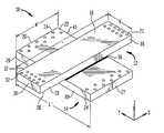
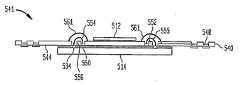
본 발명의 일실시예에 따른 마이크로전자 조립체(10)는 도 1에 도시한 바와 같이 제1 마이크로전자 소자(12) 및 제2 마이크로전자 소자(14)를 포함한다. 제1 마이크로전자 소자(12) 및 제2 마이크로전자 소자(14)는 반도체 칩, 인터포저(interposer), 회로 패널, 모듈, 칩 상의 집적 수동 소자(Integrated Passives On Chip: IPOC) 또는 다른 다양한 수동 소자 및 활성 소자일 수 있다.A
제1 마이크로전자 소자(12)는 제1 면(16)과, 이 제1 면의 반대측의 제2 면(18), 그리고 이들 제1 면(16) 및 제2 면(18)에 인접한 에지(20, 21)를 포함한다. 에지(20, 21)는 제1 마이크로전자 소자(12) 주위로 연장되는 둘레(23)의 부분이다. 제2 마이크로전자 소자(14)는 제1 면(22)과, 이 제1 면의 반대측의 제2면(24), 그리고 이들 제1 면(22) 및 제2 면(24)에 인접한 에지(26, 27)를 포함한다. 에지(26, 27)는 제2 마이크로전자 소자(14) 주위로 연장되는 둘레(28)의 부분이다.The first
제1 마이크로전자 소자(12)는 이 제1 마이크로전자 소자(12)의 제2 면(18)이 제2 마이크로전자 소자(14)의 제1 면(22)에 면하도록 제2 마이크로전자 소자(14) 위에 놓인다.The first
도 1에 도시한 바와 같이, 제1 마이크로전자 소자(12)의 에지(20, 21)는 제2 마이크로전자 소자(14)의 둘레(28)를 지나 외측 방향으로 연장되며, 제2 마이크로전자 소자(14)의 에지(26, 27)은 제1 마이크로전자 소자(12)의 둘레(23)를 지나 외측 방향으로 연장된다,
As shown in Figure 1, the
*제1 마이크로전자 소자(12)는 길이(L)와 폭(W)을 가지며, 제2 마이크로전자 소자(14)는 길이(L')와 폭(W')을 갖는다. 길이(L, L')의 치수는 폭(W, W')의 치수보다 크지만, 이것이 필수적인 것은 아니다. 또한, 도 1에 도시한 바와 같이 제1 마이크로전자 소자(12)의 길이(L)는 제2 마이크로전자 소자(14)의 길이(L')에 대해 횡방향으로 배치되며, 보다 바람직하게는 2개의 길이(L, L')는 서로 직교한다. 예시의 용이화를 위해, 도 1은 길이(L')가 Y축을 따른 방향으로 정렬되고, 길이(L)가 Y축에 대해 수직인 X축을 따른 방향으로 정렬되는 좌표계에 따라 구성된다. 2개의 마이크로전자 소자(12, 14)는 Z축을 따른 방향으로 상하로 적층된다. 본 명세서에서 설명되는 좌표계는 단지 예시의 용이화를 위해 사용되는 것이지, 임의의 중력적 위치 설정을 칭하는 것이 아니다. "상부", "저부", "상단" 및 "하단"과 같은 기술 용어는 단지 예시의 목적을 위해 유사하게 사용된다.The first
도 1에는 또한 마이크로전자 조립체(10) 내에 포함될 수 있는 다양한 특징부 중 일부의 예가 도시되어 있다. 제1 마이크로전자 소자(12)는 제1 면(16)에 노출되는 복수 개의 컨택트(32)를 포함할 수 있다. 컨택트(32)는 제1 면(16) 위로 돌출될 수도 있고, 제1 면 내로 오목할 수도 있으며, 제1 마이크로전자 요소(12)의 제1 면과 동일한 평면일 수도 있다. 제2 마이크로전자 소자(14)는 제1 면(22)에 노출되는 복수 개의 컨택트(34)를 포함할 수도 있다. 제2 마이크로전자 소자(14)의 컨택트(34)는 제1 마이크로전자 소자(12)의 컨택트(32)와 유사하게, 제2 마이크로전자 소자(14)와 다른 마이크로전자 소자 간의 전기 접속을 가능하게 한다.1 also illustrates an example of some of the various features that may be included within the
또한 도 1에 도시한 바와 같이, 제1 마이크로전사 소자(12)는 캡슐재(encapsulant material) 또는 언더필(36)에 의해 제2 마이크로전자 소자(14)에 연결될 수 있다. 캡슐재(36)는 에폭시, 실리콘 또는 다른 접착재를 포함할 수 있다. 언더필(36)은 마이크로전자 소자(12, 14)로부터 열이 소산되게 하는 열 전도성 재료일 수도 있다. 도면에 도시되어 있지는 않지만, 제1 마이크로전자 소자(12)는 마이크로전자 소자들이 서로 스냅 장착되게 하거나 함께 일체형으로 형성되게 하는 특징을 포함하는 당업계에 공지되어 있는 임의의 방법- 이것에 제한되지 않음 -에 의해 제2 마이크로전자 소자(14)에 연결 또는 부착될 수 있다. 마이크로전자 소자(12, 14)는 다양한 바이스(vice), 몰드 등에 의해 서로 일시적으로 고착될 수도 있으며, 본 명세서에서 설명하는 다양한 특징부들이 조립체에 추가된다. 특징부들이 추가된 후, 바이스를 제거할 수 있으며, 이에 따라 마이크로전자 조립체에 도포된 캡슐재가 마이크로전자 조립체(10)에 안정성과 구조를 제공한다.1, the
제1 마이크로전자 소자(12)는 에지(20, 21)뿐만 아니라 에지(37, 38)를 포함할 수도 있다. 그리고, 제2 마이크로전자 소자(14)는 에지(26, 27)뿐만 아니라 에지(39, 40)을 포함할 수도 있다. 도 1에 도시한 실시예에서, 제1 마이크로전자 소자의 에지(20)는 제2 마이크로전자 소자(14)의 에지(39)와 X축 방향으로 평행하다. 그리고, 에지(21)도 제2 마이크로전자 소자(14)의 에지(39)와 평행하다. 더욱이, 제1 마이크로전자 소자(12)의 에지(37, 38) 중 어느 하나 또는 이들 모두는 제2 마이크로전자 소자(14)의 에지(26, 27)와 Y축 방향으로 평행할 수 있다.The first
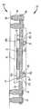
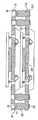
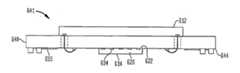
마이크로전자 조립체(10)는 도 2에 도시한 바와 같이 상면(42)과, 이 상면 반대측의 저면(44)을 갖는 기판(40)을 포함할 수 있다. 기판은 폴리이미드 또는 다른 유전체 재료로 이루어진 층을 포함할 수 있다. 기판은 당업자에 의해 알려진 임의의 공지된 성분으로 형성될 수도 있다. 솔더 마스크층(도시하지 않음)이 단일 금속층 상에 배치될 수 있다.The
본 발명의 실시예에 따른 패키지(41)는 도 2에 도시한 바와 같이 기판(40)에 연결된 도 1의 조립체를 포함할 수 있다. 기판(40)은 이 기판의 저면(44)이 제1 마이크로전자 소자(12)의 제1 면(16)에 면하도록 제1 마이크로전자 소자(12) 위에 놓이게 위치될 수 있다. 접착재(46) 또는 언더필을 사용하여 제1 마이크로전자 소자(12)를 기판(40)의 저면(44)에 연결할 수 있다. 캡슐재가 접착층이나 열 전도성 층 또는 이들 양자의 기능을 수행하는 요소로 대체될 수 있다.The
기판(40)은 도 4에 가장 잘 도시한 바와 같이 구멍(49)을 통해 기판의 상면(42)과 저면(44)에 노출되어 있는 복수 개의 단자(48)를 포함한다. 필수적인 것은 아니지만, 단자(48)는 기판의 둘레(P)를 따라 위치 설정될 수 있으며, 보다 바람직하게는 기판의 코너에 위치된다.The
도 3에 도시한 바와 같이, 기판(40)은 기판의 상면(42)에 노출되어 있는 결합 컨택트(50)를 포함할 수 있다. 결합 컨택트(50) 중 적어도 몇몇은 기판(40) 상에 또는 기판 내에 배치된 트레이스(52)에 의해 단자(48) 중 적어도 몇몇에 전기 접속된다. 기판(40)의 단자(48), 컨택트(50) 및 트레이스(52)와 같은 전기적으로 상호 접속하는 상호 접속 요소들은 2개 이상의 층으로 형성될 수 있다. 도 2 및 도 3의 실시예에서, 상호 접속 요소들은 금속으로 이루어진 단일층을 사용하여 형성된다.As shown in FIG. 3, the
기판(40)은 상면(42)에서 저면(44)까지 연장되는 복수 개의 구멍(54)도 포함한다. 본 발명의 바람직한 일실시예에서, 구멍(54)은 제1 마이크로전자 요소와 제2 마이크로전자 요소의 컨택트(32, 34) 각각과 정렬된다. 따라서, 구멍은 각각의 마이크로전자 소자 위에 놓여 이 마이크로전자 소자에 대한 접근을 허용한다. 구멍(54) 각각의 일부분은 에지(56)에 의해 형성된다.The
마이크로전자 소자(12, 14)를 기판(40)에 전기적으로 상호 접속시키기 위해, 마이크로전자 조립체(41)에 있어서 컨택트(32, 34)와 결합 컨택트(50) 사이에 전기적 상호 접속 요소가 마련될 수 있다. 전기적 상호 접속 요소는 컨택트(32, 34)에서 구멍(54)을 경유하여 에지(56)를 거쳐 결합 컨택트(50)까지 연장되는 도선(55) 형태일 수 있다. 도선(55)은 제1 마이크로전자 소자(12)와 제2 마이크로전자 소자(14)의 컨택트(32, 34)를 기판(40)의 결합 컨택트(50)에 접속시킨다.Electrical interconnection elements are provided between the
결합 컨택트(50)는 트레이스(52)에 의해 기판의 단자(48)에 접속된다. 트레이스(52)는 다양한 섹션, 각도 및 턴뿐만 아니라 슬롯의 경계를 정하는 기판의 에지(56)와 평행한, 화살표(E)로 나타낸 에지 방향으로 연장되는 전선(53)을 포함한다.The
결합 컨택트(50) 중 적어도 몇몇은 구멍(54) 근처에서 복수 행(51)으로 배치된다. 결합 컨택트의 각 행은 슬롯의 인접 에지(56)와 평행한 에지 방향으로 연장된다. 예컨대, 슬롯(54A)에 인접한 결합 컨택트의 행(51A)은 구멍(54A)의 에지(56)에 인접하게 에지 방향(E)으로 연장되는 반면, 행(51B)의 결합 컨택트는 슬롯(54B)의 에지(56)와 평행한 에지 방향으로 연장된다.At least some of the mating contacts (50) are disposed in a plurality of rows (51) near the hole (54). Each row of mating contacts extends in an edge direction parallel to the
행(51A)의 결합 컨택트는 트레이스(52)의 전선(53) 중 적어도 몇몇이 결합 컨택트와 인접한 구멍(54A)의 에지 사이에서 연장되는 결합 컨택트(50)에 연결되는, 본 명세서에서 "트레이스-근접(trace-proximate)" 구성이라고 칭하는 구성에 연결된다. 행(51A)의 결합 컨택트는 구멍의 일단에 근접한 단자(48A) 그룹에 접속된다. 이 단자 그룹에 가장 가까운 곳에 위치하는 결합 컨택트(50Aa)는 에지(56)로부터 가장 먼 곳에 위치하는 전선(53Aa)에 접속되며, 이에 따라 단자(48Aa)에 접속된다. 이 단자 그룹에서 가장 먼 곳에 위치하는 결합 컨택트(50Ac)는 에지(56)에 가장 가까운 곳에 위치하는 전선(53Ac)에 접속되며, 이에 따라 단자(48Ac)에 접속된다. 동일한 방식으로, 다른 결합 컨택트는 트레이스의 전선에 접속되고, 이에 따라 그룹(48A)의 단자에 접속된다. 단자의 접속 순서는 에지 방향(EA), 즉 단자 그룹(48)에서 멀어지는, 에지(56A)를 따른 에지 방향으로의 컨택트 위치의 순서에 대응한다.The mating contact of
행(51B)의 결합 컨택트와 트레이스는 본 명세서에서 "트레이스-원격(trace-remote)" 구성이라고 칭하는 역구성에 연결된다. 트레이스 원격 구성에서, 행의 결합 컨택트에 접속된 트레이스(52)의 전선(53) 중 몇몇은 이들 컨택트에 접속된 전선과 인접한 구멍(54B)의 에지(56) 사이에 놓인다. 행(51B)의 결합 컨택트는 동일한 단자 그룹(48A)에 접속된다. 행(51B)에서, 단자 그룹(48A)에서 가장 먼 곳에 위치하는 결합 컨택트(50Ba)는 에지(56B)에서 가장 먼 곳에 위치하는 전선(53Ba)에 접속되고, 이에 따라 단자(48Aa)에 접속된다. 단자 그룹(48A)에 가장 가까운 곳에 위치하는 결합 컨택트(50Bc)는 에지(56B)에 가장 가까운 곳에 위치하는 전선(53Bc)에 접속되고, 이에 따라 단자(48Ac)에 접속된다. 여기에서도, 행(51B)의 다른 결합 컨택트는 컨택트 위치의 순서대로 트레이스의 전선에 접속되고, 이에 따라 단자 그룹(48A)에 접속된다. 단자의 접속 순서는 에지 방향(EB), 즉 단자 그룹(48A)을 향하는, 에지(56A)를 따른 에지 방향으로의 컨택트 위치의 순서에 대응한다.The mating contacts and traces in
이러한 구성은 단자에 대한 접속 순서는 동일하지만, 교차 없이 2개의 상이한 에지 방향으로 연장되는 2개 행의 결합 단자를 제공하기 때문에, 모든 트레이스가 단일 금속층으로 형성될 수 있다. 동일하게 접속되는 행의 결합 단자로 인해 동일한 칩에 대해 공통 접속이 이루어지게 된다. 예컨대, 칩(12) 상에 있는 "IO7"이라는 라벨이 붙은 컨택트는 접속 컨택트(50Ba)에 접속되고, 이에 따라 단자(48a)에 접속되는 반면, 칩(14) 상에 있는 "IO7"이라는 라벨이 붙은 동일한 컨택트(34)는 결합 컨택트(50Aa)에 접속되고, 이에 따라 동일한 단자(48a)에 접속된다.This arrangement allows all traces to be formed into a single metal layer since the connection order to the terminals is the same but provides two rows of coupling terminals that extend in two different edge directions without crossing. A common connection is made to the same chip due to the connection terminals of the rows connected in the same way. For example, a contact labeled "IO7" on the
행(51C)에 있는 대부분의 결합 컨택트는 트레이스-근접 구성에 있어서의 단자 그룹(48B)에 접속되는 반면, 행(51D)에 있는 대부분의 결합 컨택트는 트레이스-원격 구성에 있어서의 동일한 단자 그룹(48B)에 접속된다. 여기에서도, 트레이스-원격 구성과 트레이스-근접 구성을 사용함으로써 행(51D) 내에 있는 단자 그룹(48B)에 대한 접속 순서가 교차 없이 행(51C) 내에 있는 동일한 단자에 대한 연결 순서와 동일해진다. 칩 선택(chip-enable) 결합 컨택트(50')의 세트들이 행(51C, 51D)에 산재되어 있다. 칩 선택 결합 컨택트는 추가의 트레이스에 의해 그룹(48C)에 있는 단자에 접속된다. 이러한 추가의 트레이스 중 몇몇은 행(51D)의 결합 컨택트와, 구멍(54D)의 인접 에지 사이에서 연장되는 전선(53')을 갖는다는 점에 주목하라.Most of the mating contacts in
와이어 본딩 공정에 의해 형성되는 도선(55)은 결합 컨택트를 칩의 컨택트(32, 34)에 접속시킨다. 각 행의 결합 컨택트와 관련된 와이어 본드는 인접한 에지(56)를 거쳐, 인접한 구멍(54)을 통과하여 칩 중 하나로 연장된다. 예컨대, 도 3 및 도 4에 도시한 바와 같이, 행(51A, 51C)의 결합 컨택트와 관련된 와이어 본드는 슬롯(54A, 54C)를 통과하여 연장된다. 와이어 본드 중 몇몇은 몇몇 트레이스의 전선(53)을 거쳐 연장된다. 예컨대, 트레이스-근접 구성을 갖는 열(51A, 51C)의 결합 컨택트와 관련된 와이어 본드(55)는 관련 전선을 거쳐 연장된다. 도 4에 가장 잘 도시한 바와 같이, 와이어 본드는 트레이스 위에서 고리를 형성한다. 이와 유사하게, 행(51D)에 있는 몇몇 컨택트와 관련된 와이어 본드(도 3)는 칩 선택 컨택트와 관련된 전선(53')과 교차한다. 와이어 본드는 어떠한 경우에도 칩 상의 컨택트와 결합 컨택트 간의 접속을 이루도록 마련되어야 하기 때문에 기본적으로 비용 제로(zero cost)로 교차점을 제공한다. 경미한 상향 상승에 의해 와이어 본드(55)를 형성하는 데에는 추가의 비용이 거의 수반되지 않거나 전혀 수반되지 않아, 와이어 본드가 트레이스(52)와 교차하게 된다. 전형적으로, 하나의 와이어 본드(55)가 각각의 칩 컨택트(32, 34)에 접속된다. 도 3에는 칩 선택 컨택트("CE"라는 라벨이 붙어 있음)가 칩 선택 결합 컨택트(50') 모두에 접속되어 있는 것이 도시되어 있다. 사실상, 각각의 칩 선택 컨택트는 하나의 칩 선택 결합 컨택트에만 접속되며, 이에 따라 그룹(48C)에 있는 하나의 단자에만 접속된다. 상이한 칩들은 그룹(48C)에 있는 상이한 단자에 접속된다.The
도 4에 도시한 바와 같이, 마이크로전자 조립체(41)는 기판(40)의 상면(42)에 부착되는 캡슐재(60)를 포함할 수 있다. 캡슐재(60)는 결합 컨택트(50)를 마이크로전자 소자(12,14)의 컨택트(32, 34)에 상호 접속시키는 도선(55)의 무결성을 보호 및 유지한다. 또한 도 4에 도시한 바와 같이, 단자(48)는 마이크로전자 조립체(41)가 회로 패널(62)과 같은 마이크로전자 소자에 전기 접속될 수 있게 한다. 회로 패널(62)은 이 회로 패널의 표면에 노출된 단자(64)를 포함한다. 땜납 질량체(66)와 같은 상호 전기 접속부를 사용하여 기판(42)의 단자(48)를 회로 패널(62)의 단자(64)에 전기 접속할 수 있다.As shown in FIG. 4, the
상대적으로 얇은 마이크로전자 조립체(41)의 두께로 인해, 패키지와 회로 패널(62) 간의 상호 전기 접속은 제1 마이크로전자 소자(12) 및 제2 마이크로전자 소자(14)의 위치 설정을 방해하는 일 없이 이루어질 수 있다. 추가의 캡슐재(70)가 제1 마이크로전자 소자(12)와 제2 마이크로전자 소자(14) 둘레에 배치되어 마이크로전자 소자를 기판(40)에 접속시킬 뿐만 아니라 기판의 구멍(54)을 통과하여 연장되는 도선(55)의 무결성도 유지할 수 있다.Due to the relatively thin thickness of the
도 5에 도시한 바와 같이, 마이크로전자 조립체(41)는 이 조립체 위에 제2 마이크로전자 조립체(141)가 놓이도록 위치 설정될 수 있다. 제2 마이크로전자 조립체(141)는 유사한 특징부 및 요소를 지닌 제1 마이크로전자 조립체(41)와 실질적으로 유사할 수 있다. 제2 마이크로전자 조립체(141)는 바람직하게는 기판(140)의 상면(142)과 저면(144)에 노출된 단자(148)를 갖는다. 단자(148)는, 예컨대 땜납 질량체(166)에 의해 제1 마이크로전자 조립체(41)의 단자(48)에 전기 접속될 수 있다. 상하로 적층된 2개의 반도체 패키지만이 도시되어 있지만, 본 발명은 상하로 적층된 임의의 개수의 패키지를 포함한다. 다른 변형예에서, 단자(48, 148)는 각각의 상면(42, 142)에 노출되는 것이 요구되지 않는 경우에 각각의 상면(42, 142)에 노출되지 않을 수 있다. 캡슐재가 기판(140)의 상면(142)에 부착되어 도선(155)의 무결성을 보호 및 유지할 수 있다.As shown in FIG. 5, the
도 6에 도시한 바와 같이, 제1 마이크로전자 소자(212)는 이 제1 마이크로전자 소자(212)의 에지(238)가 X축 방향으로 제2 마이크로전자 소자(214)의 에지(227)와 평행하게 제2 마이크로전자 소자(214) 위에 놓일 수 있다. 제1 마이크로전자 소자(212)의 에지(220, 221)는 제2 마이크로전자 소자(212)의 에지(239, 240) 각각을 지나 외측 방향으로 연장될 수 있다. 에지(220, 221) 모두가 제2 마이크로전자 소자의 각각의 에지를 지나 외측 방향으로 연장되는 것으로 도시하고 있지만, 이것이 필수적인 것은 아니며, 마이크로전자 소자의 하나의 에지만이 제2 마이크로전자 소자의 에지를 지나 외측 방향으로 연장될 수도 있다. 도 6에 도시한 마이크로전자 패키지(210)는 본 명세서에서 논의한 이전 실시예에 포함되는 다양한 특징부 및 요소를 포함할 수 있다. 예컨대, 기판(40)과 유사한 기판이 마이크로전자 패키지(210)와 함께 포함되어 조립체를 형성할 수 있다.As shown in Figure 6, the first
마이크로전자 소자가 직사각형 형상인 도면으로 본 발명을 설명하였다. 변형예에서, 마이크로전자 소자는 정사각형, 삼각형 타원형 및 원형- 이것에 제한되지 않음 -을 포함하는 임의의 형상을 가질 수 있다.The invention has been described in the context of a rectangular microelectronic element. In a variant, the microelectronic element may have any shape including square, triangular elliptical and circular - but not limited thereto.
도 7에 도시한 또 다른 변형예에서, 도선(355)은 기판(340)의 에지(341)를 거쳐 연장될 수 있으며, 이에 따라 제1 마이크로전자 소자(312) 및 제2 마이크로전자 소자(314) 상에 노출된 컨택트(332, 334)를 기판(340) 상에 노출된 결합 컨택트(350)에 전기 접속시킬 수 있다. 캡슐재가 마이크로전자 반도체 패키지(310) 둘레에 배치되어 패키지의 강성과 안정성을 유지할 수 있다.7, a
도 8에 도시한 바와 같이, 도 3의 마이크로전자 조립체(41)는 제1 마이크로전자 조립체(441)에 면하는 관계로 적층될 수 있다. 제2 마이크로전자 조립체(441)는 본 명세서에서 논의한 이전 실시예를 참고하여 설명한 것과 동일한 여러 가지 특징부 및 요소를 포함할 수 있다. 예시의 용이를 위해, 이들 특징부 중 몇몇은 도면에 도시하지 않는다. 2개의 마이크로전자 조립체가 서로 면하는 경우에, 제1 마이크로전자 조립체(41)의 단자(48)와 제2 마이크로전자 조립체(441)의 단자(448)도 서로 면한다. 단자(48, 448) 사이에는, 이들 단자를 접속시켜 적층된 마이크로전자 패키지를 형성하기 위해서 전기 접속부(466)가 배치될 수 있다. 예컨대, 패키지를 회로 패널에 접속시키기 위해서 기판(40) 상에 접촉 패드(도시하지 않음)를 배치할 수 있다.As shown in FIG. 8, the
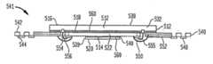
다른 변형예에서, 마이크로전자 조립체(541)는 도 9 및 도 10에 도시한 바와 같이 제1 마이크로전자 소자(512)와 제2 마이크로전자 소자(514)를 포함할 수 있다. 제1 마이크로전자 소자(512)는 제1 면(516)과 이 제1 면의 반대측의 제2 면(518)을 포함한다. 제2 마이크로전자 소자(514)도 제1 면(520)과, 이 제1 면의 반대측의 제2 면(522)를 포함한다. 마이크로전자 조립체(541)는 제1 면(542)과 제2 면(544)을 갖는 기판(540)도 포함한다. 제1 마이크로전자 소자(512)는 이 제1 마이크로전자 소자의 제2 면(518)이 기판(540)의 상면(542)에 면하도록 기판(540) 위에 놓이게 위치된다. 그리고, 제2 마이크로전자 소자(514)는 이 제2 마이크로전자 소자의 제2 면(522)이 기판의 저면(544)에 면하도록 기판(540) 아래에 놓이게 위치된다. In another variation, the
마이크로전자 소자(512, 514)는 언더필 또는 캡슐재(560)에 의해 기판(540)에 부착될 수 있다. 2개의 마이크로전자 소자(512, 514)는 기판(540)이 이들 소자 사이에 위치된다는 점을 제외하고는 본 명세서에서 논의한 이전 실시예와 유사하게 배치된다. 이에 따라, 가장 바람직한 실시예에서는 제1 마이크로전자 소자(512)의 에지(520, 521) 중 하나 이상이 제2 마이크로전자 소자(514)의 에지(539, 540) 중 하나를 넘어 외측 방향으로 연장된다. 그리고, 제2 마이크로전자 소자(514)의 에지(526, 527) 중 하나 이상은 제1 마이크로전자 소자(512)의 에지(537, 538) 중 하나를 지나 외측 방향으로 연장된다. 이에 따라, 가장 바람직한 실시예에서는 2개의 마이크로전자 소자가 이들 사이에 배치된 기판에 대해 교차 관계로 위치된다.The
제1 마이크로전자 소자(512) 및 제2 마이크로전자 소자(514)는 바람직하게는 이들 소자 각각의 제2 면(518, 522)에 노출된 컨택트(532, 534)도 포함한다. 컨택트(532, 534)는 바람직하게는 기판(540)의 상면(542)에서 저면(544)까지 연장되는 구멍(554)과 정렬된다. 기판(540)은 상면(542)이나 저면(544)과 이들 상면 및 저면 중 어느 하나 또는 이들 양자에 노출된 단자(548)와 상면 및 저면 모두에 노출된 결합 컨택트(50)를 더 포함한다. 결합 컨택트(550) 중 적어도 몇몇은 도 10에 도시한 바와 같이 트레이스(552)에 의해 단자(548) 중 적어도 몇몇에 전기 접속된다. 예시의 용이를 위해, 결합 컨택트(550)를 단자(548)에 연결하는 트레이스 중 몇 개만을 도시한다. 도 10에 도시한 바와 같이, 결합 컨택트(550)가 기판의 상면(542) 및 저면(544)에 노출되는 상태로 기판(540)의 저면(544)에 금속층을 배치할 수 있다.The first
마이크로전자 소자(512, 514)를 기판(540)에 전기 접속시키는 방법에서는, 전기적 상호 접속부, 즉 도선(555)이 컨택트(532, 534)에 부착된다. 도선(555)은 컨택트(532, 534)에서 결합 컨택트(550)에 부착될 때까지 기판의 구멍(554)을 통과하여 연장된다. 그에 따라, 도선(555)은 기판(540)의 일면- 제1 마이크로전자 소자(512)에 대한 상면(542) 및 제2 마이크로전자 소자(514)에 대한 저면(544) -에서 마이크로전자 소자(512 또는 514)에서부터 기판의 반대측 면까지 연장된다. 예컨대, 도선(555) 중 몇몇은 상면(542)에 인접한 제1 마이크로전자 소자(512)의 컨택트(532)에 부착되고, 구멍(554)을 통해 에지(556)를 거쳐 기판(540)의 반대측 저면(544), 구체적으로는 저면 상에 배치된 결합 컨택트(550)까지 연장된다. 그리고, 이와 반대로 제2 마이크로전자 소자에 접속된 도선(555)은 기판의 저면(544)에 인접한 컨택트(534)에서 상면(542), 구체적으로는 기판의 상면(542)에 노출된 결합 컨택트(550)까지 연장된다. 도선(555)을 보호하기 위해 캡슐재(561)가 도선(555) 위에 도포될 수 있다. 앞서 논의한 실시예와 유사하게, 마이크로전자 조립체(541)는 유사한 조립체 또는 다양한 다른 조립체 상에 적층되어 적층형 패키지를 형성할 수 있다.In a method of electrically connecting the
도 11에 도시한 바와 같은 변형예에서, 마이크로전자 조립체(641)는 도 9 및 도 10의 제1 마이크로전자 소자 및 기판과 유사하게 형성된 기판(640) 및 마이크로전자 소자(612)를 포함할 수 있다. 그러나, 제2 마이크로전자 소자(614)는 기판(640)의 저면(644)에서 기판에 전기적으로 상호 접속된다는 점에서 도 9 및 도 10에 도시한 제2 마이크로전자 소자와 다르다. 제2 마이크로전자 소자(614)는 바람직하게는 이 제2 마이크로전자 소자의 제2 면(622)을 따라 노출된 컨택트(634)를 포함할 수 있다. 컨택트는 볼 그리드 어레이, 스터드 범프, 도선 또는 추가의 전기 접속 기구 중 어느 하나에 의해 기판(640)에 전기 접속될 수 있다. 기판(640)은 기판의 제2 면(644)에 노출된, 제2 마이크로전자 소자의 컨택트(634)에 상호 접속될 수 있는 결합 컨택트(650)를 포함한다.11, the
도 12에 도시한 바와 같은 또 다른 변형예에서, 마이크로전자 조립체(741)는 기판(740)이, 제1 금속층(790)이 기판(740)의 상면(742)에 노출되고, 제2 금속층(791)이 기판의 저면(744)에 노출된 2개의 금속층 구성을 포함한다는 점을 제외하고는 이전 실시예와 유사하게 구성될 수 있다.12, the
이전 실시예와 같이 마이크로전자 조립체(741)는 제1 마이크로전자 소자(712)와 제2 마이크로전자 소자(714)를 포함한다. 각각의 마이크로전자 소자는 본 명세서에서 이미 논의한 방법으로 기판(740)에 부착될 수 있다. 2개의 금속층을 갖는 것으로 인한 한가지 이점은 각각의 마이크로전자 소자(712, 714)의 제1 면에 노출된 컨택트(732)에 접속하는 결합 도선(755)이 기판(740)의 결합 컨택트(750)에 결합되기 위해 기판(740)을 통과한 후 다시 기판(74) 둘레로 기판(740)을 경유하여 연장해야 할 필요가 없다는 것이다.As in the previous embodiment, the
도면에 도시하지는 않았지만, 제1 금속층(742)과 제2 금속층(745)은 각각 본 명세서에서 이전 실시예를 참고하여 논의한 바와 같은 복수 개의 단자, 트레이스 및 결합 컨택트를 포함할 수 있다.Although not shown in the figures, the
기판의 표면에 노출되는 다양한 단일 금속층의 실시예와 2개의 금속층의 실시예를 본 명세서에서 논의하였지만, 본 발명은 단일 금속층이나 2개의 금속층이 기판 내에서 노출되는 경우도 고려한다. 금속층(들)은 특정 요건에 따라 기판의 일면 또는 양면에 노출될 수 있다.Although embodiments of various single metal layers and embodiments of two metal layers that are exposed to the surface of a substrate are discussed herein, the present invention contemplates that a single metal layer or two metal layers are exposed in the substrate. The metal layer (s) may be exposed to one or both sides of the substrate according to certain requirements.
본 발명의 다른 변형예에서, 마이크로전자 조립체(841)는 본 명세서에서 설명한 임의의 실시예와 유사하게 구성될 수 있지만, 단자 대신에 또는 단자와 조합되는 전기 전도성 포스트 또는 기둥(898)도 포함할 수 있다. 도 13에 도시한 특정 일실시예에서, 기둥(898)은 기판(840)에서 하향 연장된다. 참고에 의해 개시 내용이 본 명세서에 통합되는, 공동 양도된 미국 특허 출원 제10/985,119호, 제10/985,126호 및 제11/014,439호에 개시된 바와 같이 결합 컨택트(850) 및 트레이스(852)와 조합된 기둥(898)을 구성할 수 있다.In another variation of the invention, the microelectronic assembly 841 may be constructed similar to any of the embodiments described herein, but may also include an electrically conductive post or post 898 in place of or in combination with the terminal . In the particular embodiment shown in FIG. 13, the
도면에 도시하지 않은 또 다른 변형예에서, 도 11의 제2 마이크로전자 소자(614)는 제2 마이크로전자 소자의 제1 면(620)을 따라 배치된 컨택트를 가질 수 있다. 컨택트는 도선을 이용하여 기판(640)의 저면(644)에 노출된 결합 컨택트에 부착될 수 있다. 기판은 선택적으로 추가의 트레이스층을 포함할 수 있다. 추가적으로, 구멍(54)을 긴 슬롯으로 도시하였지만, 이러한 구멍은 임의의 형상을 가질 수 있다.In another variation not shown in the drawing, the second
본 발명은 전자기기의 제조에 사용될 수 있다.The present invention can be used in the manufacture of electronic devices.
본 명세서에서는 특정 실시예들을 참고하여 본 발명을 설명하였지만, 이들 실시예는 단순히 본 발명의 원리 및 적용을 예시하는 것이라는 점을 이해해야 한다. 그에 따라, 예시적인 실시예를 다양하게 변형할 수 있고, 첨부된 청구 범위에 의해 규정되는 본 발명의 사상 및 범위에서 벗어나는 일 없이 다른 구성을 안출할 수 있다는 점을 이해해야 한다.Although the present invention has been described herein with reference to particular embodiments, it should be understood that these embodiments are merely illustrative of the principles and applications of the present invention. It is, therefore, to be understood that the illustrative embodiments may be variously modified and embodied without departing from the spirit and scope of the invention as defined by the appended claims.
Claims (19)
Translated fromKorean각각의 마이크로전자 소자는 서로 대향하는 능동 표면 및 수동 표면을 갖고, 제1 에지들이 제1 측방향에서 상기 능동 표면 및 수동 표면의 경계를 이루고, 제2 에지들이 상기 제1 측방향을 가로지르는 제2 측방향에서 상기 능동 표면 및 수동 표면의 경계를 이루고, 상기 제1 마이크로전자 소자의 수동 표면이 상기 제2 마이크로전자 소자의 능동 표면을 향하고, 상기 제1 마이크로전자 소자 및 제2 마이크로전자 소자의 마주보는 능동 표면과 수동 표면 사이에 최소의 간격도 필요로 하지 않도록 상기 제1 마이크로전자 소자가 상기 제2 마이크로전자 소자 상에 중첩되고, 상기 제1 마이크로전자 소자의 제1 에지들 각각은 상기 제2 마이크로전자 소자의 인접한 제1 에지들 각각을 넘어가도록 배치되고, 상기 제2 마이크로전자 소자의 제2 에지들 각각은 상기 제1 마이크로전자 소자의 인접한 제2 에지들 각각을 넘어가도록 배치되며,
상기 제1 마이크로전자 소자의 각각의 제1 에지는 제2 마이크로전자 소자의 각각의 제1 에지보다 짧은 길이를 갖고, 상기 제1 마이크로전자 소자의 각각의 제2 에지는 상기 제2 마이크로전자 소자의 각각의 제2 에지보다 긴 길이를 가지며,
상기 제1 마이크로전자 소자 및 제2 마이크로전자 소자는 마이크로전자 소자의 제1 에지들 및 제2 에지들로 이루어진 그룹으로부터 선택된 적어도 두 개의 대향하는 에지들에 노출되는 컨택트들을 구비하고, 상기 제2 마이크로전자 소자의 컨택트들 중 어느 것도 상기 제1 마이크로전자 소자의 수동 표면 아래에 놓이지 않으며,
상기 마이크로전자 반도체 패키지는, 제1 표면과 그에 대향하는 제2 표면을 구비하는 기판, 및 상기 제1 마이크로전자 소자와 제2 마이크로전자 소자의 컨택트들과 정렬되는 개구들을 더 포함하고, 상기 기판은 상기 제1 마이크로전자 소자와 제2 마이크로전자 소자 위에 가로놓여, 상기 기판의 제2 표면은 상기 제1 마이크로전자 소자와 제2 마이크로전자 소자의 활성 표면들을 향하고,
상기 기판은 본딩 컨택트들을 구비하고, 상기 제1 마이크로전자 소자 및 제2 마이크로전자 소자의 컨택트들은 상기 기판의 각각의 본딩 컨택트들과 전기적으로 접속되는 것인 마이크로전자 반도체 패키지.A microelectronic semiconductor package comprising a first microelectronic element and a second microelectronic element,
Each microelectronic element having opposed active and passive surfaces, wherein the first edges border the active surface and the passive surface in a first lateral direction and the second edges border the passive surface, Wherein a passive surface of the first microelectronic component is facing the active surface of the second microelectronic component and a boundary between the active surface and the passive surface of the first microelectronic component The first microelectronic element is superimposed on the second microelectronic element so that a minimum spacing between the opposing active surface and the passive surface is not required and each of the first edges of the first microelectronic element 2 < / RTI > microelectronic devices, each of the second edges of the second microelectronic device being disposed to extend beyond each of the first adjacent edges of the first microelectronic device, And each of the second edges of the microelectronic element extends beyond each of the second edges,
Wherein each first edge of the first microelectronic element has a length that is less than a respective first edge of the second microelectronic element and each second edge of the first microelectronic element has a length Has a length greater than each second edge,
Wherein the first microelectronic element and the second microelectronic element have contacts exposed to at least two opposing edges selected from the group consisting of first edges and second edges of the microelectronic element, None of the contacts of the electronic device are located below the passive surface of the first microelectronic device,
Wherein the microelectronic semiconductor package further comprises a substrate having a first surface and a second surface opposite thereto and apertures aligned with the contacts of the first microelectronic element and the second microelectronic element, The second surface of the substrate facing the active surfaces of the first microelectronic component and the second microelectronic component,
Wherein the substrate has bonding contacts and the contacts of the first microelectronic element and the second microelectronic element are electrically connected to respective bonding contacts of the substrate.
상기 제1 마이크로전자 소자는, 상기 제1 마이크로전자 소자의 길이 방향 축이 상기 제2 마이크로전자 소자의 길이 방향 축을 가로지르도록, 상기 제2 마이크로전자 소자 위에 중첩되는 것인 마이크로전자 반도체 패키지.The method of claim 1, wherein each of the first microelectronic element and the second microelectronic element has a length and a width, the length is greater than the width,
Wherein the first microelectronic element is overlaid on the second microelectronic element such that the longitudinal axis of the first microelectronic element traverses the longitudinal axis of the second microelectronic element.
청구항 1에 따른 제1 마이크로전자 반도체 패키지를 포함하고, 제2 마이크로전자 반도체 패키지를 더 포함하며, 상기 제2 마이크로전자 반도체 패키지는 상기 제1 마이크로전자 반도체 패키지 위에 가로놓이는 것인 마이크로전자 조립체.As a microelectronic assembly,
A microelectronic assembly comprising a first microelectronic semiconductor package according to claim 1, further comprising a second microelectronic semiconductor package, wherein the second microelectronic semiconductor package is laid over the first microelectronic semiconductor package.
Applications Claiming Priority (3)
| Application Number | Priority Date | Filing Date | Title |
|---|---|---|---|
| US11/291,398 | 2005-12-01 | ||
| US11/291,398US8026611B2 (en) | 2005-12-01 | 2005-12-01 | Stacked microelectronic packages having at least two stacked microelectronic elements adjacent one another |
| PCT/US2006/045817WO2007064779A1 (en) | 2005-12-01 | 2006-11-30 | Stacked microelectronic packages |
Related Parent Applications (1)
| Application Number | Title | Priority Date | Filing Date |
|---|---|---|---|
| KR1020087013790ADivisionKR101409946B1 (en) | 2005-12-01 | 2006-11-30 | Stacked microelectronic packages |
Publications (2)
| Publication Number | Publication Date |
|---|---|
| KR20130130087A KR20130130087A (en) | 2013-11-29 |
| KR101479440B1true KR101479440B1 (en) | 2015-01-06 |
Family
ID=37763826
Family Applications (2)
| Application Number | Title | Priority Date | Filing Date |
|---|---|---|---|
| KR1020087013790AActiveKR101409946B1 (en) | 2005-12-01 | 2006-11-30 | Stacked microelectronic packages |
| KR1020137029068AActiveKR101479440B1 (en) | 2005-12-01 | 2006-11-30 | Stacked microelectronic packages |
Family Applications Before (1)
| Application Number | Title | Priority Date | Filing Date |
|---|---|---|---|
| KR1020087013790AActiveKR101409946B1 (en) | 2005-12-01 | 2006-11-30 | Stacked microelectronic packages |
Country Status (5)
| Country | Link |
|---|---|
| US (3) | US8026611B2 (en) |
| JP (1) | JP5547893B2 (en) |
| KR (2) | KR101409946B1 (en) |
| CN (1) | CN101322246B (en) |
| WO (1) | WO2007064779A1 (en) |
Families Citing this family (14)
| Publication number | Priority date | Publication date | Assignee | Title |
|---|---|---|---|---|
| TWI335652B (en)* | 2007-04-04 | 2011-01-01 | Unimicron Technology Corp | Stacked packing module |
| US7994644B2 (en)* | 2007-06-01 | 2011-08-09 | Tessera, Inc. | Package stacking through rotation |
| KR101003568B1 (en)* | 2007-11-14 | 2010-12-22 | 산요 세미컨덕터 컴퍼니 리미티드 | Semiconductor Modules and Imaging Devices |
| US8390083B2 (en) | 2009-09-04 | 2013-03-05 | Analog Devices, Inc. | System with recessed sensing or processing elements |
| US8569884B2 (en) | 2011-08-15 | 2013-10-29 | Tessera, Inc. | Multiple die in a face down package |
| US8680684B2 (en)* | 2012-01-09 | 2014-03-25 | Invensas Corporation | Stackable microelectronic package structures |
| US9847462B2 (en) | 2013-10-29 | 2017-12-19 | Point Engineering Co., Ltd. | Array substrate for mounting chip and method for manufacturing the same |
| KR102161776B1 (en)* | 2014-03-28 | 2020-10-06 | 에스케이하이닉스 주식회사 | Stack package |
| JP6507779B2 (en)* | 2015-03-26 | 2019-05-08 | セイコーエプソン株式会社 | Electro-optical device, method of manufacturing electro-optical device, and electronic apparatus |
| US9666558B2 (en) | 2015-06-29 | 2017-05-30 | Point Engineering Co., Ltd. | Substrate for mounting a chip and chip package using the substrate |
| KR102379704B1 (en) | 2015-10-30 | 2022-03-28 | 삼성전자주식회사 | semiconductor package |
| US20180114786A1 (en)* | 2016-10-21 | 2018-04-26 | Powertech Technology Inc. | Method of forming package-on-package structure |
| KR102149387B1 (en) | 2019-02-13 | 2020-08-28 | 삼성전기주식회사 | Electronic component module |
| US20240096859A1 (en)* | 2022-08-19 | 2024-03-21 | Google Llc | Socket To Support High Performance Multi-die ASICs |
Citations (2)
| Publication number | Priority date | Publication date | Assignee | Title |
|---|---|---|---|---|
| JPH02312265A (en)* | 1989-05-26 | 1990-12-27 | Mitsubishi Electric Corp | Semiconductor device |
| JPH04155954A (en)* | 1990-10-19 | 1992-05-28 | Nec Kyushu Ltd | Semiconductor device |
Family Cites Families (35)
| Publication number | Priority date | Publication date | Assignee | Title |
|---|---|---|---|---|
| US5198888A (en) | 1987-12-28 | 1993-03-30 | Hitachi, Ltd. | Semiconductor stacked device |
| US4956694A (en) | 1988-11-04 | 1990-09-11 | Dense-Pac Microsystems, Inc. | Integrated circuit chip stacking |
| US7198969B1 (en) | 1990-09-24 | 2007-04-03 | Tessera, Inc. | Semiconductor chip assemblies, methods of making same and components for same |
| FR2670322B1 (en)* | 1990-12-05 | 1997-07-04 | Matra Espace | SOLID STATE MEMORY MODULES AND MEMORY DEVICES CONTAINING SUCH MODULES |
| CA2117092A1 (en) | 1991-09-06 | 1993-03-18 | Dan C. Yingling | Automatic door operator |
| US5468994A (en) | 1992-12-10 | 1995-11-21 | Hewlett-Packard Company | High pin count package for semiconductor device |
| US5325268A (en) | 1993-01-28 | 1994-06-28 | National Semiconductor Corporation | Interconnector for a multi-chip module or package |
| US5585667A (en) | 1994-12-23 | 1996-12-17 | National Semiconductor Corporation | Lead frame for handling crossing bonding wires |
| US5998864A (en)* | 1995-05-26 | 1999-12-07 | Formfactor, Inc. | Stacking semiconductor devices, particularly memory chips |
| US5721452A (en)* | 1995-08-16 | 1998-02-24 | Micron Technology, Inc. | Angularly offset stacked die multichip device and method of manufacture |
| US5861666A (en) | 1995-08-30 | 1999-01-19 | Tessera, Inc. | Stacked chip assembly |
| US5841191A (en)* | 1997-04-21 | 1998-11-24 | Lsi Logic Corporation | Ball grid array package employing raised metal contact rings |
| US6072233A (en) | 1998-05-04 | 2000-06-06 | Micron Technology, Inc. | Stackable ball grid array package |
| US6020629A (en)* | 1998-06-05 | 2000-02-01 | Micron Technology, Inc. | Stacked semiconductor package and method of fabrication |
| US6388833B1 (en)* | 1998-06-29 | 2002-05-14 | Western Digital Technologies, Inc. | Method for manufacturing a disk drive having an overwriteable clock track |
| US6215193B1 (en)* | 1999-04-21 | 2001-04-10 | Advanced Semiconductor Engineering, Inc. | Multichip modules and manufacturing method therefor |
| JP2001077301A (en) | 1999-08-24 | 2001-03-23 | Amkor Technology Korea Inc | Semiconductor package and its manufacturing method |
| JP3798597B2 (en) | 1999-11-30 | 2006-07-19 | 富士通株式会社 | Semiconductor device |
| US6252305B1 (en)* | 2000-02-29 | 2001-06-26 | Advanced Semiconductor Engineering, Inc. | Multichip module having a stacked chip arrangement |
| US20020043709A1 (en) | 2000-10-13 | 2002-04-18 | Yeh Nai Hua | Stackable integrated circuit |
| US6404648B1 (en)* | 2001-03-30 | 2002-06-11 | Hewlett-Packard Co. | Assembly and method for constructing a multi-die integrated circuit |
| JP4454181B2 (en) | 2001-05-15 | 2010-04-21 | 富士通マイクロエレクトロニクス株式会社 | Semiconductor device |
| TW502406B (en) | 2001-08-01 | 2002-09-11 | Siliconware Precision Industries Co Ltd | Ultra-thin package having stacked die |
| DE10142120A1 (en)* | 2001-08-30 | 2003-03-27 | Infineon Technologies Ag | Electronic component has semiconductor chips whose passive back sides are fastened to top side of carrier substrate and active chip surface, respectively |
| TW523890B (en)* | 2002-02-07 | 2003-03-11 | Macronix Int Co Ltd | Stacked semiconductor packaging device |
| DE10227305A1 (en) | 2002-06-19 | 2003-09-04 | Siemens Dematic Ag | Electrical multiple layer component module used in polymer stud grid array technology comprises a second three-dimensional substrate arranged on first three-dimensional substrate with intermediate connections connected to contacts |
| ES2426255T3 (en)* | 2002-06-28 | 2013-10-22 | Boston Scientific Neuromodulation Corporation | Microstimulator that has a built-in power source and a two-way telemetry system |
| US6737742B2 (en) | 2002-09-11 | 2004-05-18 | International Business Machines Corporation | Stacked package for integrated circuits |
| US6825064B2 (en) | 2002-09-30 | 2004-11-30 | Ultratera Corporation | Multi-chip semiconductor package and fabrication method thereof |
| JP4076841B2 (en) | 2002-11-07 | 2008-04-16 | シャープ株式会社 | Manufacturing method of semiconductor device |
| KR20050001159A (en)* | 2003-06-27 | 2005-01-06 | 삼성전자주식회사 | Multi-chip package having a plurality of flip chips and fabrication method thereof |
| US7176043B2 (en) | 2003-12-30 | 2007-02-13 | Tessera, Inc. | Microelectronic packages and methods therefor |
| US7709968B2 (en) | 2003-12-30 | 2010-05-04 | Tessera, Inc. | Micro pin grid array with pin motion isolation |
| US8207604B2 (en) | 2003-12-30 | 2012-06-26 | Tessera, Inc. | Microelectronic package comprising offset conductive posts on compliant layer |
| US7402911B2 (en)* | 2005-06-28 | 2008-07-22 | Infineon Technologies Ag | Multi-chip device and method for producing a multi-chip device |
- 2005
- 2005-12-01USUS11/291,398patent/US8026611B2/enactiveActive
- 2006
- 2006-11-30KRKR1020087013790Apatent/KR101409946B1/enactiveActive
- 2006-11-30WOPCT/US2006/045817patent/WO2007064779A1/enactiveApplication Filing
- 2006-11-30JPJP2008543449Apatent/JP5547893B2/ennot_activeExpired - Fee Related
- 2006-11-30KRKR1020137029068Apatent/KR101479440B1/enactiveActive
- 2006-11-30CNCN2006800452483Apatent/CN101322246B/enactiveActive
- 2011
- 2011-09-27USUS13/246,242patent/US8890327B2/ennot_activeExpired - Fee Related
- 2014
- 2014-10-31USUS14/529,279patent/US9627366B2/enactiveActive
Patent Citations (2)
| Publication number | Priority date | Publication date | Assignee | Title |
|---|---|---|---|---|
| JPH02312265A (en)* | 1989-05-26 | 1990-12-27 | Mitsubishi Electric Corp | Semiconductor device |
| JPH04155954A (en)* | 1990-10-19 | 1992-05-28 | Nec Kyushu Ltd | Semiconductor device |
Also Published As
| Publication number | Publication date |
|---|---|
| JP5547893B2 (en) | 2014-07-16 |
| WO2007064779A8 (en) | 2008-06-26 |
| US8026611B2 (en) | 2011-09-27 |
| US20070126102A1 (en) | 2007-06-07 |
| US20120013028A1 (en) | 2012-01-19 |
| KR20080073739A (en) | 2008-08-11 |
| US9627366B2 (en) | 2017-04-18 |
| US20150048524A1 (en) | 2015-02-19 |
| US8890327B2 (en) | 2014-11-18 |
| KR101409946B1 (en) | 2014-06-20 |
| WO2007064779A1 (en) | 2007-06-07 |
| JP2009518825A (en) | 2009-05-07 |
| CN101322246B (en) | 2011-12-21 |
| CN101322246A (en) | 2008-12-10 |
| KR20130130087A (en) | 2013-11-29 |
Similar Documents
| Publication | Publication Date | Title |
|---|---|---|
| KR101479440B1 (en) | Stacked microelectronic packages | |
| KR101925427B1 (en) | Stackable microelectronic package structures | |
| US7402911B2 (en) | Multi-chip device and method for producing a multi-chip device | |
| JP6033843B2 (en) | Multi-die face-down stacking for two or more dies | |
| US7050303B2 (en) | Semiconductor module with vertically mounted semiconductor chip packages | |
| US7550857B1 (en) | Stacked redistribution layer (RDL) die assembly package | |
| KR101413220B1 (en) | Semiconductor package having interposer and method for manufacturing semiconductor package | |
| KR20160090706A (en) | Semiconductor package with narrow width interposer | |
| JP2002076057A5 (en) | ||
| WO2014134118A1 (en) | Microelectronic package with consolidated chip structures | |
| JP2001077294A (en) | Semiconductor device | |
| JP2009506571A (en) | MICROELECTRONIC DEVICE HAVING INTERMEDIATE CONTACTS FOR CONNECTING TO INTERPOSER SUBSTRATE AND METHOD OF PACKAGING MICROELECTRONIC DEVICE WITH INTERMEDIATE CONTACTS RELATED TO THE SAME | |
| TW201733062A (en) | Flipped die stacks with multiple rows of leadframe interconnects | |
| CN117832205A (en) | Chip packaging structure and electronic equipment | |
| KR100513422B1 (en) | Mounting structure in integrated circuit module | |
| KR20040078807A (en) | Ball Grid Array Stack Package | |
| US20040159925A1 (en) | Semiconductor device and method for manufacture thereof | |
| KR100810349B1 (en) | Interposers and Semiconductor Packages Using the Same | |
| JP4402806B2 (en) | Semiconductor device | |
| KR100612783B1 (en) | Semiconductor device | |
| US20240379525A1 (en) | Semiconductor package stack and a method for forming the same | |
| KR20150125960A (en) | Microelectronic package with consolidated chip structures | |
| JP2002270760A (en) | Electronic component, assembly thereof and its manufacturing method |
Legal Events
| Date | Code | Title | Description |
|---|---|---|---|
| A107 | Divisional application of patent | ||
| PA0104 | Divisional application for international application | Comment text:Divisional Application for International Patent Patent event code:PA01041R01D Patent event date:20131101 | |
| PG1501 | Laying open of application | ||
| A201 | Request for examination | ||
| PA0201 | Request for examination | Patent event code:PA02012R01D Patent event date:20131202 Comment text:Request for Examination of Application | |
| E902 | Notification of reason for refusal | ||
| PE0902 | Notice of grounds for rejection | Comment text:Notification of reason for refusal Patent event date:20140203 Patent event code:PE09021S01D | |
| E902 | Notification of reason for refusal | ||
| PE0902 | Notice of grounds for rejection | Comment text:Notification of reason for refusal Patent event date:20140530 Patent event code:PE09021S01D | |
| E701 | Decision to grant or registration of patent right | ||
| PE0701 | Decision of registration | Patent event code:PE07011S01D Comment text:Decision to Grant Registration Patent event date:20140929 | |
| GRNT | Written decision to grant | ||
| PR0701 | Registration of establishment | Comment text:Registration of Establishment Patent event date:20141229 Patent event code:PR07011E01D | |
| PR1002 | Payment of registration fee | Payment date:20141229 End annual number:3 Start annual number:1 | |
| PG1601 | Publication of registration | ||
| FPAY | Annual fee payment | Payment date:20171213 Year of fee payment:4 | |
| PR1001 | Payment of annual fee | Payment date:20171213 Start annual number:4 End annual number:4 | |
| FPAY | Annual fee payment | Payment date:20181211 Year of fee payment:5 | |
| PR1001 | Payment of annual fee | Payment date:20181211 Start annual number:5 End annual number:5 | |
| PR1001 | Payment of annual fee | Payment date:20201217 Start annual number:7 End annual number:7 | |
| PR1001 | Payment of annual fee | Payment date:20211220 Start annual number:8 End annual number:8 | |
| PR1001 | Payment of annual fee | Payment date:20221222 Start annual number:9 End annual number:9 | |
| PR1001 | Payment of annual fee | Payment date:20231219 Start annual number:10 End annual number:10 | |
| PR1001 | Payment of annual fee | Payment date:20241217 Start annual number:11 End annual number:11 |