KR101478810B1 - Power storage device - Google Patents
Power storage deviceDownload PDFInfo
- Publication number
- KR101478810B1 KR101478810B1KR20070074107AKR20070074107AKR101478810B1KR 101478810 B1KR101478810 B1KR 101478810B1KR 20070074107 AKR20070074107 AKR 20070074107AKR 20070074107 AKR20070074107 AKR 20070074107AKR 101478810 B1KR101478810 B1KR 101478810B1
- Authority
- KR
- South Korea
- Prior art keywords
- capacitor
- power supply
- circuit
- antenna
- control circuit
- Prior art date
- Legal status (The legal status is an assumption and is not a legal conclusion. Google has not performed a legal analysis and makes no representation as to the accuracy of the status listed.)
- Expired - Fee Related
Links
Images


Classifications
- H—ELECTRICITY
- H10—SEMICONDUCTOR DEVICES; ELECTRIC SOLID-STATE DEVICES NOT OTHERWISE PROVIDED FOR
- H10D—INORGANIC ELECTRIC SEMICONDUCTOR DEVICES
- H10D84/00—Integrated devices formed in or on semiconductor substrates that comprise only semiconducting layers, e.g. on Si wafers or on GaAs-on-Si wafers
- H10D84/80—Integrated devices formed in or on semiconductor substrates that comprise only semiconducting layers, e.g. on Si wafers or on GaAs-on-Si wafers characterised by the integration of at least one component covered by groups H10D12/00 or H10D30/00, e.g. integration of IGFETs
- H10D84/811—Combinations of field-effect devices and one or more diodes, capacitors or resistors
- H—ELECTRICITY
- H01—ELECTRIC ELEMENTS
- H01Q—ANTENNAS, i.e. RADIO AERIALS
- H01Q1/00—Details of, or arrangements associated with, antennas
- H01Q1/36—Structural form of radiating elements, e.g. cone, spiral, umbrella; Particular materials used therewith
- H—ELECTRICITY
- H01—ELECTRIC ELEMENTS
- H01Q—ANTENNAS, i.e. RADIO AERIALS
- H01Q1/00—Details of, or arrangements associated with, antennas
- H01Q1/36—Structural form of radiating elements, e.g. cone, spiral, umbrella; Particular materials used therewith
- H01Q1/38—Structural form of radiating elements, e.g. cone, spiral, umbrella; Particular materials used therewith formed by a conductive layer on an insulating support
- H—ELECTRICITY
- H01—ELECTRIC ELEMENTS
- H01Q—ANTENNAS, i.e. RADIO AERIALS
- H01Q7/00—Loop antennas with a substantially uniform current distribution around the loop and having a directional radiation pattern in a plane perpendicular to the plane of the loop
- H—ELECTRICITY
- H01—ELECTRIC ELEMENTS
- H01Q—ANTENNAS, i.e. RADIO AERIALS
- H01Q9/00—Electrically-short antennas having dimensions not more than twice the operating wavelength and consisting of conductive active radiating elements
- H01Q9/04—Resonant antennas
- H01Q9/16—Resonant antennas with feed intermediate between the extremities of the antenna, e.g. centre-fed dipole
- H01Q9/28—Conical, cylindrical, cage, strip, gauze, or like elements having an extended radiating surface; Elements comprising two conical surfaces having collinear axes and adjacent apices and fed by two-conductor transmission lines
- H01Q9/285—Planar dipole
- H—ELECTRICITY
- H02—GENERATION; CONVERSION OR DISTRIBUTION OF ELECTRIC POWER
- H02J—CIRCUIT ARRANGEMENTS OR SYSTEMS FOR SUPPLYING OR DISTRIBUTING ELECTRIC POWER; SYSTEMS FOR STORING ELECTRIC ENERGY
- H02J50/00—Circuit arrangements or systems for wireless supply or distribution of electric power
- H02J50/005—Mechanical details of housing or structure aiming to accommodate the power transfer means, e.g. mechanical integration of coils, antennas or transducers into emitting or receiving devices
- H—ELECTRICITY
- H02—GENERATION; CONVERSION OR DISTRIBUTION OF ELECTRIC POWER
- H02J—CIRCUIT ARRANGEMENTS OR SYSTEMS FOR SUPPLYING OR DISTRIBUTING ELECTRIC POWER; SYSTEMS FOR STORING ELECTRIC ENERGY
- H02J50/00—Circuit arrangements or systems for wireless supply or distribution of electric power
- H02J50/10—Circuit arrangements or systems for wireless supply or distribution of electric power using inductive coupling
- H02J50/12—Circuit arrangements or systems for wireless supply or distribution of electric power using inductive coupling of the resonant type
- H—ELECTRICITY
- H02—GENERATION; CONVERSION OR DISTRIBUTION OF ELECTRIC POWER
- H02J—CIRCUIT ARRANGEMENTS OR SYSTEMS FOR SUPPLYING OR DISTRIBUTING ELECTRIC POWER; SYSTEMS FOR STORING ELECTRIC ENERGY
- H02J50/00—Circuit arrangements or systems for wireless supply or distribution of electric power
- H02J50/20—Circuit arrangements or systems for wireless supply or distribution of electric power using microwaves or radio frequency waves
- H02J50/27—Circuit arrangements or systems for wireless supply or distribution of electric power using microwaves or radio frequency waves characterised by the type of receiving antennas, e.g. rectennas
- H—ELECTRICITY
- H02—GENERATION; CONVERSION OR DISTRIBUTION OF ELECTRIC POWER
- H02J—CIRCUIT ARRANGEMENTS OR SYSTEMS FOR SUPPLYING OR DISTRIBUTING ELECTRIC POWER; SYSTEMS FOR STORING ELECTRIC ENERGY
- H02J50/00—Circuit arrangements or systems for wireless supply or distribution of electric power
- H02J50/50—Circuit arrangements or systems for wireless supply or distribution of electric power using additional energy repeaters between transmitting devices and receiving devices
Landscapes
- Engineering & Computer Science (AREA)
- Computer Networks & Wireless Communication (AREA)
- Power Engineering (AREA)
- Charge And Discharge Circuits For Batteries Or The Like (AREA)
- Details Of Aerials (AREA)
Abstract
Translated fromKoreanDescription
Translated fromKorean본 발명은 상용(商用) 전력으로부터 전력을 공급받지 않고 충전을 할 수 있는 축전 장치에 관한 것이다.BACKGROUND OF THE
휴대 전화기, 모바일 컴퓨터, 디지털 카메라, 디지털 오디오 플레이어 등 전자기기의 소형화가 진행되어, 다종 다양한 제품이 시장에 출하되고 있다. 이와 같은 휴대형 전자기기는 구동용 전원으로서 2차 전지를 내장하고 있다. 2차 전지로서는 리튬 이온 전지나 니켈 수소 전지 등이 사용되고 있다. 2차 전지의 충전은 상용 전력으로부터 전력을 공급 받아 행해지고 있다. 예를 들어, 이용자는 각 가정에 설치되어 있는 콘센트에 AC 어댑터를 접속하여 2차 전지의 충전을 행하고 있다.BACKGROUND ART Electronic devices such as mobile phones, mobile computers, digital cameras, and digital audio players have been miniaturized, and various products have been shipped to the market. Such a portable electronic device incorporates a secondary battery as a driving power source. As the secondary battery, a lithium ion battery, a nickel hydride battery, or the like is used. Charging of the secondary battery is performed by receiving power from commercial power. For example, a user connects an AC adapter to an outlet provided in each home to charge the secondary battery.
휴대형 전자기기는 편리하지만, 그 사용 시간은 2차 전지의 용량에 따라 제한을 받고 있다. 이 전자기기의 사용자는 2차 전지의 잔량에 주위를 기울여야 하고, 충전 시간을 항상 신경 써야 하는 상황에 있다. 또한, 전자기기의 충전 플러그는 기기마다 또는 기종마다 상이하므로, 많은 AC 어댑터를 소지하는 것이 요구되었다.Portable electronic devices are convenient, but their use time is limited by the capacity of the secondary battery. The user of this electronic device has to pay attention to the remaining amount of the secondary battery and to always pay attention to the charging time. Further, since the charging plug of the electronic device is different for each device or each model, it has been required to have a large number of AC adapters.
이것에 대하여, 코일이 감겨진 슬라이드 내에서 영구 자석을 왕복 운동시켜 전자 유도 기전력을 발생시킴으로써 충전하는 축전 장치가 개시되어 있다(예를 들어, 문헌 1 참조). 이 축전지에 의하면, 상용 전원으로부터 전력을 공급 받지 않고 충전할 수 있다고 되어 있다.On the other hand, a power storage device has been disclosed in which a permanent magnet is reciprocated in a slide in which a coil is wound to generate an electromagnetic induction electromotive force (see, for example, Document 1). According to this battery, it is said that the battery can be charged without receiving power from a commercial power source.
[문헌 1] 일본국 공개특허공고 2006-149163호 공보(도 1, 4 페이지)[Patent Document 1] Japanese Unexamined Patent Application Publication No. 2006-149163 (Figs. 1 and 4)
그러나, 코일과 영구 자석에 의한 전자 유도 기전력을 이용하는 것은 가동부가 필요하고, 구조적으로 소형화하는 것은 적합하지 않다. 또한, 그와 같은 축전 장치에서는 자석이 소지되어 운동해야 하지만, 영구 자석을 사용하기 때문에 중량이 증가하게 된다. 따라서, 종래의 축전 장치는 체적 및 중량이 증가하여 휴대성을 해친다는 문제가 있다.However, moving parts are required to use the electromagnetic induction electromotive force by the coils and the permanent magnets, and it is not suitable to make the structure smaller. In such a power storage device, the magnet must be held and moved. However, since the permanent magnet is used, the weight is increased. Therefore, the conventional power storage device has a problem of deteriorating the portability due to an increase in volume and weight.
그런데, 휴대 전화기 등 이동체를 대상으로 한 지상 디지털 방송의 원 세그먼트(one segment) 부분 수신 서비스 "원세그(1-seg)"가 제공되는 등, 휴대형 전자기기 분야에서는 금후, 보다 소형 경량이고, 1회의 충전으로 장시간 사용할 수 있는 것이 요구되고 있다. 따라서, 소형 경량이고, 상용 전력으로부터 전력을 공급 받지 않고 충전을 할 수 있는 축전 장치에 대한 요구는 높아지고 있다.[0004] In the field of portable electronic devices, a one-segment part-receiving service "1-segment " of terrestrial digital broadcasting for mobile devices such as mobile phones is provided. It is demanded that it can be used for a long time by charging. Therefore, there is a growing demand for a compact and lightweight power storage device capable of charging without receiving power from commercial power.
그래서, 본 발명은, 소형 경량화 또는 경량 박형화를 도모하면서 충전을 간편하게 하고, 상용 전력으로부터 전력을 공급 받지 않고 충전을 할 수 있는 축전 장치를 제공하는 것을 목적으로 한다. 또한, 그와 같은 축전 장치를 소형 경량화한 경우에도, 튼튼함을 유지하고 요구되는 기능을 유지하는 것을 목적으로 한다.SUMMARY OF THE INVENTION It is therefore an object of the present invention to provide a power storage device capable of simplifying charging while reducing the size, weight and thickness of a battery, and charging the battery without receiving power from commercial power. It is also an object of the present invention to maintain the robustness and maintain the required function even when the electrical storage device is reduced in size and weight.
본 발명은, 전자파를 수신하는 안테나와, 전력을 저장하는 커패시터와, 전력의 저장 및 공급을 제어하는 회로를 구비한 축전 장치이다. 그리고, 안테나, 커패시터, 제어 회로를 일체 구조로 함과 동시에 박형화하는 경우에, 세라믹스 등으로 형성되는 구조체를 일부에 사용하는 것을 요지로 한다.The present invention is a power storage device including an antenna for receiving electromagnetic waves, a capacitor for storing electric power, and a circuit for controlling the storage and supply of electric power. In addition, when the antenna, the capacitor, and the control circuit are integrally formed and thinned, a structure formed by ceramics or the like is used in part.
세라믹스 등으로 형성되는 구조체는, 외부로부터 가해지는 압압이나 굽힘 응력에 대하여 내성을 가지므로, 안테나나 제어 회로를 박형화한 경우에, 보호체로서 기능한다. 또한, 이 구조체에 커패시터로서의 기능을 가지게 할 수도 있다.The structure formed of ceramics or the like has resistance to pressing and bending stress externally applied, and thus functions as a protector when the antenna and the control circuit are made thin. In addition, this structure may have a function as a capacitor.
본 발명에 의하면, 안테나에 의해 전자파를 수신하고, 그 전력을 커패시터에 충전하는 회로 및 임의로 방전하는 제어 회로를 구비함으로써, 축전 장치의 수명을 늘릴 수 있다.According to the present invention, the life of the power storage device can be increased by including a circuit for receiving electromagnetic waves by the antenna, for charging the capacitor with the electric power, and a control circuit for discharging arbitrarily.
세라믹스 등으로 형성되는 구조체를 축전 장치의 일부에 사용함으로써, 강성(剛性)을 높일 수 있다. 그것에 의해, 축전 장치를 박형화한 경우에도, 튼튼함을 유지하고 요구되는 기능을 유지할 수 있다.By using a structure formed of ceramics or the like in a part of the electrical storage device, the rigidity can be increased. Thereby, even when the power storage device is thinned, it is possible to maintain the robustness and to maintain the required function.
예를 들어, 펜 끝 등 뾰족한 물체에 의한 압압이 가해졌을 때에도, 커패시터나 제어 회로에 응력이 가해져 동작 불량이 되는 것을 방지할 수 있다. 굽힘 응력에 대해서도 내성을 가지게 할 수 있다. 또한, 세라믹스 등으로 형성되는 구조체에 접속용 배선을 형성하고, 안테나와 제어 회로를 접속함으로써, 굽힘 응력이 가해져도 접속부가 빠져 동작 불량을 일으키는 것을 방지할 수 있다.For example, even when pressure is applied by a pointed object such as a pen tip, stress is applied to the capacitor or the control circuit, thereby preventing malfunction. It is possible to have resistance against bending stress. Further, by forming a wiring for connection in a structure formed of ceramics or the like, and connecting the antenna and the control circuit, it is possible to prevent a faulty operation from occurring due to the lack of connection portions even when bending stress is applied.
[실시형태 1][Embodiment 1]
본 발명의 실시형태에 대하여 도면을 사용하여 아래에 설명한다. 그러나, 본 발명은 아래의 설명에 한정되는 것은 아니고, 본 발명의 취지 및 그 범위로부터 벗어남이 없이 그의 형태 및 상세한 사항을 다양하게 변경할 수 있다는 것은 당업자라면 용이하게 이해할 수 있을 것이다. 따라서, 본 발명은 아래에 나타내는 실시형태의 기재 내용에 한정하여 해석되는 것은 아니다. 또한, 아래에 설명하는 본 발명의 구성에서 같은 것을 가리키는 부호는 다른 도면 사이에 공통되어 사용하는 경우가 있다.Embodiments of the present invention will be described below with reference to the drawings. However, it is to be understood that the present invention is not limited to the following description, and that various changes in form and detail thereof may be made by those skilled in the art without departing from the spirit and scope of the present invention. Therefore, the present invention is not construed as being limited to the contents of the embodiments described below. In addition, the same reference numerals in the configurations of the present invention described below may be commonly used among other drawings.
본 발명에 따른 축전 장치는, 안테나가 형성된 제1 구조체와, 상층 및 하층의 절연층 사이에 끼워진 반도체층을 가지고, 이 반도체층으로 형성된 전력 공급 제어 회로와, 제1 구조체보다 높은 강성을 가지고 커패시터가 형성된 제2 구조체를 가지고 있다. 이 제2 구조체는 적어도 내부에 유전체층을 가지고, 그 유전체층을 사용하여 커패시터가 형성되어 있는 것이 바람직하다. 제2 구조체를 세라믹스 등, 강성이 높은 것으로 형성함으로써, 전력 공급 제어 회로를 박형화하여도 축전 장치의 기계적 강도를 유지할 수 있다.A power storage device according to the present invention includes a power supply control circuit having a first structure in which an antenna is formed and a semiconductor layer sandwiched between upper and lower insulating layers and formed of the semiconductor layer; And a second structure formed with the second structure. It is preferable that the second structure has at least a dielectric layer therein and a capacitor is formed using the dielectric layer. By forming the second structure with a high rigidity such as ceramics, the mechanical strength of the power storage device can be maintained even if the power supply control circuit is made thin.
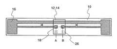
도 1에 이와 같은 축전 장치의 일 양태를 나타낸다. 제1 구조체(10)는 절연 재료로 형성되어 있다. 제1 구조체(10)의 두께는 1 ㎛∼100 ㎛, 바람직하게는 5 ㎛∼30 ㎛로 한다. 절연 재료로서는, 플라스틱 시트, 플라스틱 필름, 유리 에폭시 수지, 유리판, 종이, 부직포 등 다양한 것을 적용할 수 있다. 제1 구조체(10)의 적어도 한쪽 면에는, 도전성 재료로 안테나(16)가 형성되어 있다. 안테나의 구조는 축전 장치가 이용하는 전자파의 주파수대에 따라 다르게 하는 것이 바람직하다. 단파대(주파수 1∼30 MHz의 전자파), 초단파대(주파수 30∼300 MHz의 전자파), 극초단파대(주파수 0.3∼3 GHz의 전자파)의 주파수를 적용하는 경우에는, 그 주파수 에 적합한 안테나 형상으로 하면 좋다. 도 1은 다이폴 안테나로서, 초단파대, 극초단파대의 통신에 적합한 안테나를 나타내고 있다. 안테나는 도 1에 나타내는 바와 같은 다이폴 안테나 외에, 모노폴 안테나, 패치 안테나, 스파이럴 안테나, 루프 안테나 등을 적용할 수 있다.Fig. 1 shows an embodiment of such a power storage device. The
안테나(16)에는, 전력 공급 제어 회로(14)와 접속하기 위하여 안테나 단자(18)가 제공되어 있다. 전력 공급 제어 회로(14)는 적어도 일부가 제1 구조체(10)와 겹치도록 설치되어 있다. 제1 구조체(10)와 전력 공급 제어 회로(14)의 접속을 강고하게 하기 위하여 연결체로서 제2 구조체(12)가 사용되고 있다.The
도 2는 도 1의 A-B 절단선에 따른 축전 장치의 단면 구조를 나타내고 있다. 제1 구조체(10)의 안테나 단자(18)가 형성되어 있는 면에는, 제2 구조체(12)가 대향하도록 배치되어 있다. 제2 구조체(12)의 다른 쪽 면에는 전력 공급 제어 회로(14)가 대향하도록 배치되어 있다. 제2 구조체(12)에는, 안테나 단자(18)에 대응하는 위치에 관통 전극(20)이 형성되어 있다. 관통 전극(20)은 제2 구조체(12)의 다른 쪽 면에서, 전력 공급 제어 회로(14)의 접속 전극(24)과 접속할 수 있도록 형성되어 있다. 관통 전극(20)은 제2 구조체(12)에 형성된 관통 구멍에 금속박이나 금속 페이스트를 사용하여 형성되어 있다.Fig. 2 shows a cross-sectional structure of a power storage device taken along line A-B in Fig. On the surface of the
제2 구조체(12)는 두께가 0.1 ㎛∼50 ㎛, 바람직하게는 5 ㎛∼30 ㎛의 두께를 가지고, 제1 구조체(10)와 비교하여 경질인 것이 바람직하다. 또한, 제2 구조체(12)는 인성(靭性)을 가지고 일정한 굽힘 응력에 대해서는 탄성을 가지고 있는 것이 보다 바람직하다. 제1 구조체(10)가 플라스틱 필름이나 부직포 등의 가요성 재료로 형성되어 있는 경우에, 제2 구조체(12)에 일정한 탄성력을 가지게 함으로써, 굽힘 응력을 분산시킬 수 있기 때문이다. 그것에 의해, 관통 전극(20)을 통하여 접속되는 안테나 단자(18)와 접속 전극(24)이 단선(斷線)하는 고장을 없앨 수 있다. 또한, 제2 구조체(12)의 내측에 관통 전극(20)을 형성함으로써, 전력 공급 제어 회로(14)를 소형화할 수 있다.The
제2 구조체(12)로서는, 절연 물질로서 경질 플라스틱, 유리 등을 사용할 수 있지만, 특히 세라믹스 재료를 사용하여 형성하는 것이 바람직하다. 세라믹스 재료는 상기 특성을 발현시키기 때문에 소재의 선택지가 넓고, 또한 다수의 세라믹스를 조합시켜 복합화할 수 있기 때문이다.As the
세라믹스 재료의 대표예로서는, 고절연성 재료로서 알루미나(Al2O3)를 사용하는 것이 바람직하다. 또한, 고용량성 재료로서 티탄산 바륨(BaTiO3)을 사용하는 것이 바람직하다. 기계적 강도를 우선시키기 위해서는 알루미나(Al2O3), 산화티탄(TiOx), 탄화규소(SiC), 강화 유리, 결정화 유리를 사용하는 것이 바람직하다. 또한, SiC의 나노 입자를 Si3N4에 첨가한 복합 세라믹스, 육방정 BN을 포함하는 복합 세라믹스를 사용하면, 고강도, 내산화, 고인성이 얻어질 수 있으므로 바람직하다.As a representative example of the ceramics material, alumina (Al2 O3 ) is preferably used as the high-insulating material. It is preferable to use barium titanate (BaTiO3 ) as a high-capacity material. It is preferable to use alumina (Al2 O3 ), titanium oxide (TiOx ), silicon carbide (SiC), tempered glass, or crystallized glass in order to give priority to mechanical strength. Further, when a composite ceramics in which SiC nanoparticles are added to Si3 N4 or a composite ceramics including hexagonal BN is used, high strength, oxidation resistance and toughness can be obtained, which is preferable.
이와 같은 세라믹스 재료를 사용하고, 하나의 층의 두께를 0.1 ㎛∼2 ㎛로 하여, 다수의 층을 적층한 형태로 하여도 좋다. 즉, 적층 기판으로서 각 층에 전 극을 형성하여 적층형 커패시터를 형성하는 것이 바람직하다.By using such a ceramics material, one layer may have a thickness of 0.1 占 퐉 to 2 占 퐉, and a plurality of layers may be laminated. That is, it is preferable to form an electrode in each layer as a laminated substrate to form a laminated capacitor.
전력 공급 제어 회로(14)는 두께 5 nm∼500 nm, 바람직하게는 30 nm∼150 nm의 반도체층으로 형성된 능동 소자로 회로가 형성되어 있다. 반도체층의 하층 및 상층측에는 절연층이 형성되어 있다. 이들 절연층은 반도체층을 보호하기 위한 층으로서 형성된다. 또한, 게이트 절연층과 같이 기능층으로서 이용되는 일도 있다. 능동 소자는 대표예로서 전계효과 트랜지스터가 형성된다. 상술한 바와 같이 반도체층이 박막인 점에서, 여기서 형성되는 전계효과 트랜지스터는 박막트랜지스터라고도 불린다. 반도체층은 기상 성장법, 스퍼터링법 등에 의해 형성된 반도체층을 열 처리 및/또는 레이저 빔 등의 에너지 빔의 조사에 의해 결정화시킨 결정성 반도체층을 사용하는 것이 바람직하다. 결정성 반도체층에 의해, 전계효과 트랜지스터의 전계효과 이동도가 30∼500 cm2/V·sec(전자)가 되고, 전력 손실을 억제할 수 있기 때문이다.The power
전력 공급 제어 회로(14)는 반도체층, 절연층, 배선을 형성하는 층을 포함하고, 합계 0.5∼5 ㎛의 두께로 형성하는 것이 바람직하다. 이 두께로 형성함으로써, 축전 장치의 박형화에 기여할 수 있다. 또한, 굽힘 응력에 대하여 내성을 가지게 할 수 있다. 이 경우에, 반도체층을 섬 형상으로 분리하여 형성함으로써, 굽힘 응력에 대한 내성을 향상시킬 수 있다.The power
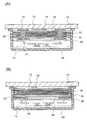
제1 구조체(10)와 제2 구조체(12)는 안테나 단자(18)와 관통 전극(20)이 전기적으로 접속하도록 접착재(28)로 고정된다. 예를 들어, 접착재(28)로서 도전성 입자를 분산시킨 아크릴, 우레탄 또는 에폭시계 접착재를 사용할 수 있다. 또한, 안테나 단자(18)와 관통 전극(20)과의 접속을 도전성 페이스트 또는 땜납 페이스트로 형성하고, 다른 부분에 아크릴, 우레탄 또는 에폭시계 접착재를 형성하여 굳혀도 좋다. 제2 구조체(12)와 전력 공급 제어 회로(14)도 마찬가지이고, 관통 전극(20)과 접속 전극(24)이 전기적으로 접속하도록 고정한다.The
봉지재(封止材)(30)는 아크릴, 우레탄, 페놀, 에폭시 또는 실리콘계 수지 재료로 형성하고, 전력 공급 제어 회로(14)를 보호하기 위하여 마련하는 것이 바람직하다. 봉지재(30)는 전력 공급 제어 회로(14)가 덮이도록 형성하고, 전력 공급 제어 회로(14), 제2 구조체(12)의 옆끝면이 덮이도록 형성하는 것이 바람직하다. 이 봉지재(30)에 의해, 전력 공급 제어 회로(14)가 손상되는 것을 막을 수 있다. 또한, 전력 공급 제어 회로(14)와 제2 구조체(12) 및 제1 구조체(10)와의 접착 강도를 높일 수 있다. 이와 같이 하여, 2 ㎛∼150 ㎛, 바람직하게는 10 ㎛∼60 ㎛의 축전 장치를 얻을 수 있다.It is preferable that the sealing
도 3은 제1 구조체(10)의 안테나 단자(18)와 전력 공급 제어 회로(14)의 접속 전극(24)을 대향시켜 배치하고, 이들을 접속하는 구조를 나타내고 있다. 제2 구조체(12)는 전력 공급 제어 회로(14)를 보호하도록 배면에 배치하고 있다. 제2 구조체(12)에 커패시터를 형성하는 경우에는, 전력 공급 제어 회로(14)에 세라믹스 안테나 접속 전극(27)을 형성하고, 제2 구조체(12)의 커패시터 외부 전극(22)과 전기적으로 접속하도록 하여도 좋다. 제1 구조체(10), 제2 구조체(12) 및 전력 공급 제어 회로(14)는 접착재(28)로 고정하는 것이 바람직하다. 도 3의 구성에서는, 전 력 공급 제어 회로(14)의 배면에 제2 구조체(12)가 설치되어 있으므로, 봉지재(30)는 적절히 마련하면 좋다.3 shows a structure in which the
이상과 같이, 본 발명에 따른 축전 장치는 세라믹스 등으로 형성되는 구조체를 사용함으로써, 축전 장치의 강성을 높일 수 있다. 그것에 의해, 축전 장치를 박형화한 경우에도, 튼튼함을 유지하고 요구되는 기능을 유지할 수 있다. 세라믹스 등으로 형성되는 구조체에 접속용 배선을 형성하여, 안테나와 전력 공급 제어 회로를 접속함으로써, 굽힘 응력이 가해지더라도 접속부가 빠져 동작 불량을 일으키는 것을 방지할 수 있다.As described above, the electrical storage device according to the present invention can increase the rigidity of the electrical storage device by using a structure formed of ceramics or the like. Thereby, even when the power storage device is thinned, it is possible to maintain the robustness and to maintain the required function. A connection wiring is formed in a structure formed of ceramics or the like and the antenna and the power supply control circuit are connected to each other so that the connection part can be prevented from being defective even if the bending stress is applied.
[실시예 1][Example 1]
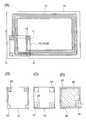
본 실시예는 안테나가 형성된 제1 구조체, 커패시터가 형성된 제2 구조체, 및 전력 공급 제어 회로(14)를 조합한 축전 장치의 일례에 대하여 도 4 및 도 5를 참조하여 설명한다. 또한, 도 4는 이 축전 장치의 평면도이고, 도 5는 A-B 절단선, C-D 절단선에 대응하는 단면도를 나타낸다.The present embodiment will be described with reference to Figs. 4 and 5 with respect to an example of a power storage device in which a first structure in which an antenna is formed, a second structure in which a capacitor is formed, and a power
도 4(A)는 제1 구조체(10)에 코일 형상의 안테나(16)가 형성되어 있는 형태를 나타내고 있다. 제1 구조체(10)는 PET(폴리에틸렌 테레프탈레이트), PEN(폴리에틸렌 나프탈레이트), PES(폴리에테르술폰), 폴리프로필렌, 폴리프로필렌 설파이드, 폴리카보네이트, 폴리에테르이미드, 폴리페닐렌 설파이드, 폴리페닐렌 옥사이드, 폴리술폰, 폴리프탈아미드, 아크릴, 폴리이미드 등의 플라스틱 재료나 부직포, 종이 등의 절연 재료로 형성한다.Fig. 4 (A) shows a configuration in which a coil-shaped
안테나(16)는 제1 구조체(10)에 인쇄법, 도금법 등에 의해, 구리, 은, 알루 미늄 등의 저저항 금속 재료를 사용하여 형성한다. 도 4에서는 안테나(16)의 형상으로서 코일 형상의 것을 나타내고 있지만, 이것은 전자(電磁) 유도 방식(예를 들어, 13.56 MHz대)을 적용하는 경우에 적합하다. 마이크로파 방식(예를 들어, UHF대(860∼960 MHz대), 2.45 GHz대 등)을 적용하는 경우에는, 신호의 전송에 사용하는 전자파의 파장을 고려하여 안테나로서 기능하는 도전층의 길이 등의 형상을 적절히 설정하면 좋다. 이 경우에는, 모노폴 안테나, 다이폴 안테나, 패치 안테나 등을 형성하면 좋다.The
도 4(A)는 안테나 단자(18)에 맞추어 제2 구조체(12), 전력 공급 제어 회로(14)가 설치되어 있는 상태를 나타내고 있다. 도 4(B)는 제2 구조체(12)의 평면도이고, 도 4(C)는 전력 공급 제어 회로(14)의 평면도이다. 제2 구조체(12)와 전력 공급 제어 회로(14)의 외형 치수는 대략 동일하게 하는 것이 바람직하다. 또는, 제2 구조체(12)보다도 전력 공급 제어 회로(14)의 외형 치수를 작게 하여도 좋다.Fig. 4 (A) shows a state in which the
본 실시예에서, 제2 구조체(12)는 세라믹스 재료로 형성되어 있는 것이 바람직하다. 이 제2 구조체(12)에는 관통 전극(20) 및 커패시터 전극(34)이 형성되어 있다. 전력 공급 제어 회로(14)에는 안테나 단자(18)와 접속하는 접속 전극(24)과 커패시터 전극(34)과 접속하는 커패시터부 접속 전극(26)이 형성되어 있다. 다음에, 제2 구조체(12) 및 전력 공급 제어 회로(14)의 접속 구조의 상세한 사항에 대하여 도 5를 참조하여 설명한다.In this embodiment, it is preferable that the
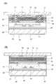
도 5(A)는 A-B 절단선에 대응하는 단면도를 나타내고 있다. 제1 구조체(10) 와 전력 공급 제어 회로(14)는 제2 구조체(12)에 형성된 관통 전극(20)에 의해 접속되어 있다. 이들은 접착재(28)에 의해 고정되어 있다. 제2 구조체(12)는 유전체층(32)과 커패시터 전극(34)이 형성된 층이, 번갈아 맞물리도록 적층되어 있다. 이와 같이 유전체층(32)과 커패시터 전극(34)을 적층함으로써 커패시터를 형성하고 있다.5 (A) is a cross-sectional view corresponding to a cutting line A-B. The
유전체층(32)은 티탄산 바륨(BaTiO3), 티탄산 스트론튬(SrTiO3), 납 복합 페로브스카이트 화합물 재료 등의 세라믹스 재료에 바인더 화합물, 가소제 및 유기 용제를 함유하는 세라믹스 페이스트를 기판 위에 도포하여 유전체층을 형성한다. 그 위에 구리 또는 구리 합금, 니켈 또는 니켈 합금, 은 또는 은 합금, 주석 또는 주석 합금으로부터 선택되는 전극 페이스트를 인쇄하여 커패시터 전극(34)을 형성한다. 또한, 관통 전극(20)을 형성하는 경우에는, 그 해당 위치에 개구가 형성되는 형상으로 한다. 이들을 건조시킨 후, 소정의 크기로 분단하고, 커패시터 전극(34)이 번갈아 맞물리도록 다수층 적층한다. 이것을 세라믹스 재료로 형성된 보호층(36) 사이에 끼우고, 탈바인더, 소성 및 열 처리를 실시함으로써 형성된다.
도 5에서, 유전체층(32) 및 커패시터 전극(34)은 나노 입자를 사용함으로써 1 ㎛∼10 ㎛의 두께로 형성할 수 있다. 그것에 의해, 2 ㎛ 두께의 유전체층(32)을 5층 적층하면 두께는 10 ㎛가 된다. 또한, 1 ㎛의 두께의 유전체층(32)을 10층 중첩하여도 10 ㎛의 두께로 끝낼 수 있다.In Fig. 5, the
도 5(B)는 C-D 절단선에 대응하는 단면도로서, 커패시터 전극(34)과 전력 공 급 제어 회로(14)의 커패시터부 접속 전극(26)의 구조를 나타내고 있다. 제2 구조체(12)에서, 외주부에 형성되는 커패시터 외부 전극(22)은 니켈 도금이나 주석 도금 등이 실시되어 있다. 커패시터 외부 전극(22)과 커패시터부 접속 전극(26)의 접속에는 접착재(28)에 의해 형성할 수 있다.5 (B) is a cross-sectional view corresponding to line C-D, showing the structure of the
이상과 같이, 안테나가 형성된 제1 구조체(10), 커패시터가 형성된 제2 구조체(12), 및 전력 공급 제어 회로(14)를 조합한 축전 장치가 얻어진다. 세라믹스 등으로 형성되는 제2 구조체(12)를 사용함으로써, 축전 장치의 강성을 높일 수 있다. 그것에 의해, 전력 공급 제어 회로(14)를 가지는 축전 장치를 박형화한 경우에도, 튼튼함을 유지하고 요구되는 기능을 유지할 수 있다.As described above, a power storage device is obtained by combining the
[실시예 2][Example 2]
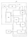
본 실시예는 다수의 안테나를 장비한 본 발명에 따른 축전 장치의 일례에 대하여 설명한다. 안테나가 형성된 제1 구조체(10), 커패시터가 형성된 제2 구조체(12), 전력 공급 제어 회로(14), 및 세라믹스 안테나(38)를 조합한 축전 장치의 일례에 대하여 도 6 및 도 7을 참조하여 설명한다. 또한, 도 6은 이 축전 장치의 평면도이고, 도 7은 E-F 절단선, G-H 절단선에 대응하는 단면도를 나타낸다.The present embodiment will describe an example of a power storage device according to the present invention equipped with a plurality of antennas. 6 and 7 for an example of a power storage device in which a
도 6(A)은 제1 구조체(10)에 코일 형상의 안테나(16)가 형성되어 있다. 안테나(16)는 실시예 1과 마찬가지로 통신에 사용하는 주파수대에 따라 형상을 적절히 변경할 수 있다.6 (A), a coil-shaped
도 6(A)은 안테나 단자(18)에 맞추어 제2 구조체(12), 전력 공급 제어 회로(14), 세라믹스 안테나(38)가 설치되어 있는 상태를 나타내고 있다. 또한, 도 6(B)은 제2 구조체(12)의 평면도이고, 도 6(C)은 전력 공급 제어 회로(14)의 평면도이고, 도 6(D)은 세라믹스 안테나(38)의 평면도이다. 제2 구조체(12), 전력 공급 제어 회로(14) 및 세라믹스 안테나(38)의 외형 치수는 대략 동일하게 하는 것이 바람직하다. 또는, 제2 구조체(12) 및 세라믹스 안테나(38)보다도 전력 공급 제어 회로(14)의 외형 치수를 작게 하여도 좋다.6A shows a state in which the
제2 구조체(12)는 세라믹스 재료로 형성되고, 관통 전극(20) 및 커패시터 외부 전극(22)이 형성되어 있다. 전력 공급 제어 회로(14)에는 안테나 단자(18)와 접속하는 접속 전극(24)과, 커패시터 외부 전극(22)과 접속하는 커패시터부 접속 전극(26), 세라믹스 안테나(38)와 접속하는 세라믹스 안테나 접속 전극(27)이 형성되어 있다. 다음에, 제2 구조체(12) 및 전력 공급 제어 회로(14)의 접속 구조의 상세한 사항에 대하여 도 7을 참조하여 설명한다.The
도 7(A)은 E-F 절단선에 대응하는 단면도를 나타내고 있다. 제2 구조체(12)는 실시예 1과 마찬가지로 세라믹스 재료로 커패시터가 형성되어 있다. 제1 구조체(10)의 안테나 단자(18)와 전력 공급 제어 회로(14)의 접속 전극(24)을 접속하는 관통 전극(20)을 가지는 구조는 도 5(A)와 마찬가지이다. 전력 공급 제어 회로(14)의 배면에는 세라믹스 안테나(38)가 배치되어 있다. 전력 공급 제어 회로(14)를 끼우는 제2 구조체(12)와 세라믹스 안테나(38)는 보호층으로서의 기능을 겸비하고 있다.7 (A) shows a cross-sectional view corresponding to the cutting line E-F. The
도 7(B)은 G-H 절단선에 대응하는 단면도로서, 전력 공급 제어 회로(14)와 세라믹스 안테나(38)의 접속 구조를 나타내고 있다. 세라믹스 안테나(38)는 유전 체(42)의 한쪽(전력 공급 제어 회로(14)측)에 접지체(44)가 형성되고, 다른 쪽에 반사체(46)가 형성되어 있다. 전력 공급 제어 회로(14)에는 세라믹스 안테나 접속 전극(27)이 형성되고, 이것에 접지체(44)와 급전체(40)가 접속하고 있다. 반사체(46)에는 지향성을 높이기 위한 슬릿이 형성되어 있어도 좋다. 반사체(46)와 급전체(40)는 간격을 가지고 배치되고, 용량 결합되어 있다.7 (B) is a cross-sectional view corresponding to the G-H cut line, showing the connection structure of the power
본 실시예의 축전 장치는, 제1 구조체(10)에 형성된 안테나(16)와 세라믹스 안테나(38)를 급전용 안테나로서 사용하고, 제2 구조체(12)에 형성된 커패시터에 충전한다. 커패시터는 유전체층(32)과 커패시터 전극(34)으로 형성되어 있다. 이 유전체층(32)과 커패시터 전극(34)을 다수층 겹침으로써 큰 용량을 형성할 수 있다. 이 경우, 안테나(16)와 세라믹스 안테나(38)가 수신하는 전자파의 주파수를 상이하게 함으로써, 효율 좋게 커패시터에 충전할 수 있다. 즉, 커패시터에 충전하기 위하여 수신하는 전자파의 대역을 넓힐 수 있다. 이 경우에, 유전체층(32) 및 커패시터 전극(34)은 나노 입자를 사용함으로써 1 ㎛∼10 ㎛의 두께로 형성할 수 있다. 그것에 의해, 2 ㎛의 두께로 유전체층(32)을 5층 적층하면 두께는 10 ㎛가 된다. 또한, 1 ㎛ 두께의 유전체층(32)을 10층 중첩하여도 10 ㎛의 두께로 끝낼 수 있다.The power storage device of the present embodiment uses the
이상과 같이, 안테나가 형성된 제1 구조체(10), 커패시터가 형성된 제2 구조체(12), 전력 공급 제어 회로(14), 및 세라믹스 안테나(38)를 조합한 축전 장치가 얻어진다. 세라믹스 등으로 형성되는 제2 구조체(12) 및 세라믹스 안테나(38)를 이용함으로써, 축전 장치의 강성을 높일 수 있다. 그것에 의해, 전력 공급 제어 회로(14)를 가지는 축전 장치를 박형화한 경우에도, 튼튼함을 유지하고 요구되는 기능을 유지할 수 있다.As described above, a power storage device is obtained by combining the
[실시예 3][Example 3]
본 발명에 따른 축전 장치의 전력 공급 제어 회로의 일례에 대하여, 도 8에 나타내는 블록도를 사용하여 설명한다.An example of the power supply control circuit of the power storage device according to the present invention will be described with reference to the block diagram shown in Fig.
도 8의 축전 장치(100)는 안테나(102), 전력 공급 제어 회로(104), 커패시터(106)로 구성되어 있다. 전력 공급 제어 회로(104)는 정류 회로(108), 저주파 신호 발생 회로(110), 스위치 회로(112), 전원 회로(114)로 구성된다. 전력 공급 제어 회로에 있어서의 전원 회로로부터, 축전 장치의 외부에 있는 부하(118)에 전력을 출력한다.The
실시예 1과의 관련에 있어서, 안테나(102)는 제1 구조체(10)에 형성되어 있다. 커패시터(106)는 제2 구조체(12)에 형성되어 있다. 전력 공급 제어 회로(104)는 전력 공급 제어 회로(14)에 상당한다.In connection with the first embodiment, the
또한, 도 8에서의 부하(118)의 구성은 전자기기에 따라 다르다. 예를 들어, 휴대 전화기나 디지털 비디오 카메라에 있어서는, 논리 회로, 증폭 회로, 메모리 컨트롤러 등이 부하에 상당한다. 또한, IC 카드, IC 태그 등에서는 고주파 회로 및 논리 회로 등이 부하에 상당한다.The configuration of the
또한, 도 8에는 급전기(120)가 발하는 전자파를 안테나(102)가 수신하여 커패시터(106)에 충전하는 구성의 축전 장치(100)를 나타낸다. 도 8에서, 안테나(102)가 수신한 전자파는 정류 회로(108)로 정류되어, 커패시터(106)에 충전한 다. 또한, 안테나(102)로 전자파를 수신함으로써 얻어진 전력은 정류 회로(108)를 통하여 저주파 신호 발생 회로(110)에 입력된다. 또한, 안테나(102)로 전자파를 수신함으로써 얻어진 전력은 정류 회로(108) 및 스위치 회로(112)를 통하여 전원 회로(114)에 신호로서 입력된다. 또한, 저주파 신호 발생 회로(110)는 입력되는 신호에 의해 동작이 제어되고, 스위치 회로(112)에 대하여, 온 오프의 제어 신호를 출력한다.8 shows a
도 8에서, 전자파를 수신함으로써 얻어지는 전력은 커패시터(106)에 충전된다. 급전기(120)로부터 충분한 전력의 공급을 받게 되지 않을 경우에는, 커패시터(106)로부터 공급되는 전력이 스위치 회로(112)를 통하여 전원 회로(114)에 전력이 공급된다. 급전기(120)는 안테나(102)가 수신할 수 있는 전자파를 방사하는 기기이다.In Fig. 8, the electric power obtained by receiving the electromagnetic wave is charged in the
도 8에서의 안테나(102)의 구성은, 전자(電磁) 결합 방식, 전자 유도 방식 또는 마이크로파 방식 등, 수신하는 전자파의 주파수대에 따라 선택하면 좋다. 안테나(102)는 급전기(120)가 공급하는 전자파의 유무에 상관없이, 임의로 전자파를 수신하여 전력 공급 제어 회로(104)에 신호를 공급할 수 있다. 예를 들어, 축전 장치(100)의 커패시터(106)를 충전하기 위하여 안테나(102)로 수신하는 전자파로서 휴대 전화기의 전자파(800∼900 MHz대, 1.5 GHz, 1.9∼2.1 GHz대 등), 휴대 전화기로부터 발진되는 전자파, 전파 시계의 전자파(40 kHz 등), 가정용의 교류 전원의 노이즈(60 Hz 등), 다른 무선 신호 출력 수단으로부터 무작위로 생기는 전자(電磁) 등을 이용할 수 있다.The configuration of the
다음에, 도 8에 나타내는 축전 장치(100)에, 전자파를 수신하여, 커패시터(106)의 충전 및 전원 회로(114)에의 전력 공급을 행하는 동작에 대하여 설명한다. 안테나(102)로 수신한 전자파는 정류 회로(108)에 의해 반파 정류되고 평활화된다. 그리고, 정류 회로(108)로부터 출력되는 전력은 스위치 회로(112)를 통하여 전원 회로(114)에 공급되고, 잉여 전력이 커패시터(106)에 저장된다.Next, a description will be given of the operation of charging the
본 실시예의 축전 장치(100)는 전자파의 강도에 따라 간헐적으로 동작시킴으로써, 커패시터(106)에 충전한 전력이 낭비되지 않도록 고안되어 있다. 일반적으로 축전 회로는 부하에 대하여 상시 전력을 공급하지만, 용도에 따라서는 반드시 상시 전력의 공급을 하지 않아도 좋은 경우도 있다. 그와 같은 경우에, 축전 장치(100)로부터의 전력 공급의 동작을 정지함으로써, 커패시터(106)에 저장한 전력의 소비를 억제할 수 있다. 본 실시예에서, 상시 동작하고 있는 것은 도 8에서의 저주파 신호 발생 회로(110)뿐이다. 저주파 신호 발생 회로(110)는 커패시터(106)에 저장된 전력을 기초로 동작한다. 도 9를 사용하여, 저주파 신호 발생 회로(110)의 출력 파형에 대하여 설명한다.The
도 9에는, 저주파 신호 발생 회로(110)가 스위치 회로에 출력하는 신호의 파형에 대하여 나타내고 있다. 도 9의 예에서는 출력 파형의 듀티를 1 : n(n은 정수(整數))으로 함으로써, 소비 전력을 1/(n+1) 정도로 할 수 있다. 이 신호를 기초로 하여 스위치 회로(112)를 구동한다. 스위치 회로(112)는 커패시터(106)와 전원 회로(114)를 출력 신호가 하이로 되어 있는 기간만 접속하고, 그것에 따라, 그 기간만 축전 장치의 배터리로부터 전원 회로를 통하여 부하에 전력이 공급된다.9 shows a waveform of a signal that the low-frequency
도 10은 도 8의 저주파 신호 발생 회로(110)의 일례를 나타낸다. 도 10의 저주파 신호 발생 회로(110)는 링 오실레이터(122), 분주(分周) 회로(124), AND 회로(126), 인버터(128), 인버터(130)로 구성되어 있다. 링 오실레이터(122)의 발진 신호를 분주 회로(124)로 분주하고, 그 출력을 AND 회로(126)에 입력하고 있다. 그리고, AND 회로(126)로 저(低)듀티비의 신호를 만들어 내고 있다. 또한, AND 회로(126)의 출력을 인버터(128) 및 인버터(130)를 통하여, 트랜스미션 게이트(132)로 구성되는 스위치 회로(112)에 입력하고 있다. 링 오실레이터(122)는 저주파수로 발진하는 것이고, 예를 들어, 1 KHz로 발진시키고 있다.Fig. 10 shows an example of the low-frequency
도 11은 도 10에서 나타낸 저주파 신호 발생 회로(110)로부터 출력되는 신호의 타이밍 차트를 나타낸다. 도 11은 링 오실레이터(122)의 출력 파형, 분주 회로(124)의 출력 파형, 및 AND 회로(126)의 출력 파형의 일례를 나타내고 있다. 도 11은 링 오실레이터(122)로부터 출력된 신호를 1024 분주하는 경우의 출력 파형을 나타내고 있다. 출력 파형은 분주 회로 출력 파형 1, 분주 회로 출력 파형 2, 분주 회로 출력 파형 3이 순차로 출력된다. 이들 출력 파형을 AND 회로(126)로 처리하면, 듀티비 1 : 1024의 신호를 형성할 수 있다. 이때 링 오실레이터(122)의 발진 주파수가 1 KHz이면 하나의 주기에서 동작 기간은 0.5 μsec, 비동작 기간은 512 μsec가 된다.11 shows a timing chart of a signal output from the low-frequency
저주파 신호 발생 회로(110)로부터 출력되는 신호는 정기적으로 스위치 회로(112)의 트랜스미션 게이트(132)의 온과 오프를 제어하여, 커패시터(106)로부터 전원 회로(114)에의 전력 공급을 제어한다. 그것에 의해, 축전 장치(100)로부터의 부하에의 전력 공급을 제어할 수 있다. 즉, 커패시터(106)로부터 신호 제어 회로부에의 전력 공급을 간헐적으로 행함으로써, 축전 장치(100)로부터 부하(118)에의 전력 공급을 억제하여 저소비전력화를 행할 수 있다.The signal output from the low frequency
도 8의 전원 회로(114)의 예에 대하여 도 12를 사용하여 설명한다. 전원 회로(114)는 기준 전압 회로와 버퍼 증폭기로 구성된다. 기준 전압 회로는 저항(134), 다이오드 접속된 트랜지스터(136, 138)에 의해 구성되어 있다. 이 회로에 의해, 트랜지스터(136, 138)에 의해, 트랜지스터의 게이트·소스간 전압(Vgs)에 따른 기준 전압(2×Vgs)을 발생시키고 있다. 버퍼 증폭기는 트랜지스터(140, 142)로 구성되는 차동 회로, 트랜지스터(144, 146)로 구성되는 커런트 미러(current mirror) 회로, 전류 공급용 저항(148), 트랜지스터(150), 저항(152)에 의해 구성되는 소스 접지 증폭기로 구성된다.An example of the
도 12에 나타내는 전원 회로(114)에서, 출력 단자로부터 흐르는 전류가 클 때는 트랜지스터(150)에 흐르는 전류가 적어지고, 또한, 출력 단자로부터 흐르는 전류가 작을 때는 트랜지스터(150)에 흐르는 전류가 많아진다. 이것에 의해, 저항(152)에 흐르는 전류는 거의 일정하게 되도록 동작한다. 또한, 출력 단자의 전위는 기준 전압 회로와 거의 같은 값이 된다. 여기서는 기준 전압 회로와 버퍼 증폭기를 가지는 전원 회로를 나타냈지만, 전원 회로(114)로서는 도 12에 한정되지 않고, 다른 형식의 전원 회로이어도 좋다.In the
상기한 바와 같이, 본 실시예의 전력 제어 회로를 실시예 1의 축전 장치에 적용할 수 있다. 본 실시예의 전력 제어 회로에 의하면, 전자파를 수신하고, 그것 을 전력으로 하여 커패시터에 충전할 수 있다. 커패시터(106)에 충전한 전력은 부하에 공급할 수 있다. 또한, 축전 장치로부터의 부하에의 전력 공급을 제어할 수 있다. 즉, 커패시터로부터 신호 제어 회로부에의 전력 공급을 간헐적으로 행함으로써, 축전 장치로부터 부하에의 전력 공급을 억제하여 저소비전력화를 행할 수 있다.As described above, the power control circuit of this embodiment can be applied to the power storage device of the first embodiment. According to the power control circuit of this embodiment, it is possible to receive electromagnetic waves and to charge the capacitor with electric power. The power charged in the
[실시예 4][Example 4]
본 실시예는 실시예 2에 대응하는 축전 장치의 일례를 도 13을 참조하여 설명한다. 또한, 이하의 설명에서는 도 8과 다른 점을 중심으로 설명한다.This embodiment will be described with reference to Fig. 13, an example of a power storage device corresponding to the second embodiment. In the following description, the difference from FIG. 8 will be mainly described.
도 13은 다수의 안테나 회로를 구비하는 축전 장치의 구성에 대하여 나타낸다. 도 8과 다른 점은 다수의 안테나 회로로서 안테나(102), 제2 안테나(103)를 구비하는 점에 있다. 안테나(102) 및 제2 안테나(103)는 적합한 수신 주파수가 다르도록 구성되어 있는 것이 바람직하다. 예를 들어, 실시예 2의 도 6에서 나타내는 바와 같이, 안테나(102)를 스파이럴 안테나로 구성하고, 제2 안테나(103)를 세라믹스 안테나(패치 안테나)로 구성할 수 있다.Fig. 13 shows a configuration of a power storage device having a plurality of antenna circuits. The difference from FIG. 8 is that the
실시예 2와의 관련에 있어서, 안테나(102)는 제1 구조체(10)에 형성되어 있다. 제2 안테나(103)는 세라믹스 안테나(38)에 상당한다. 커패시터(106)는 제2 구조체(12)에 형성되어 있다. 전력 공급 제어 회로(104)는 전력 공급 제어 회로(14)에 상당한다.In connection with the second embodiment, the
안테나(102) 및 제2 안테나(103)가 수신한 전자파는 정류 회로(108)로 정류되어 커패시터(106)에 충전된다. 정류 회로(108)에서는, 양방의 안테나가 수신한 전자파를 동시에 정류하여 커패시터(106)에 충전하도록 할 수 있다. 또한, 정류 회로(108)에서, 안테나(102) 및 제2 안테나(103)가 수신한 전자파에서, 전계 강도가 강한 쪽의 전자파를 우선적으로 정류하여 커패시터(106)에 충전하도록 하여도 좋다.The electromagnetic wave received by the
본 실시예의 축전 장치(100)에서, 다른 구성은 도 8과 마찬가지이고, 같은 작용 효과를 얻을 수 있다.In the
[실시예 5][Example 5]
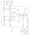
본 실시예는, 커패시터에 충전한 전력의 공급을 제어하는 기능을 구비한 축전 장치에 대하여 나타낸다. 또한, 본 실시예에서, 실시예 3에 나타내는 것과 같은 기능을 가지는 것에 대해서는 같은 부호를 붙여 설명한다.The present embodiment shows a power storage device having a function of controlling supply of electric power charged in a capacitor. In the present embodiment, those having the same functions as those in the third embodiment are denoted by the same reference numerals.
도 14의 축전 장치(100)는 안테나(102), 전력 공급 제어 회로(104), 커패시터(106)에 의해 구성되어 있다. 전력 공급 제어 회로(104)는 정류 회로(108), 제어 회로(116), 저주파 신호 발생 회로(110), 스위치 회로(112), 전원 회로(114)에 의해 구성된다. 부하(118)에의 전력 공급은 전원 회로(114)로부터 행해진다.The
실시예 1과의 관련에 있어서, 안테나(102)는 제1 구조체(10)에 형성되어 있다. 커패시터(106)는 제2 구조체(12)에 형성되어 있다. 전력 공급 제어 회로(104)는 전력 공급 제어 회로(14)에 상당한다.In connection with the first embodiment, the
본 실시예의 축전 장치는 전력 공급 제어 회로(104)가 정류 회로(108)로부터 출력되는 전력이 부하(118)의 소비전력에 대해서 잉여인 경우에는, 그 잉여분의 전력을 커패시터(106)에 저장하도록 한다. 또한, 정류 회로(108)로부터 출력되는 전 력이 부하(118)의 소비전력에 대하여 부족한 경우에는 커패시터(106)를 방전하여 전원 회로(114)에 전력을 공급한다. 도 14에서, 정류 회로(108)의 후단에 있는 제어 회로(116)는 이와 같은 동작을 행하기 위하여 제공되어 있다.When the power output from the rectifying
도 15에 제어 회로(116)의 일례를 나타낸다. 제어 회로(116)는 스위치(154), 스위치(156), 정류 소자(158), 정류 소자(160) 및 전압 비교 회로(162)를 가지고 있다. 도 15에서, 전압 비교 회로(162)는 커패시터(106)로부터 출력되는 전압과 정류 회로(108)로부터 출력되는 전압을 비교한다. 정류 회로(108)로부터 출력되는 전압이 커패시터(106)로부터 출력되는 전압보다 충분히 높을 때에는 전압 비교 회로(162)는 스위치(154)를 온으로 하고, 스위치(156)를 오프로 한다. 이 상태에서, 정류 회로(108)로부터 정류 소자(158) 및 스위치(154)를 통하여 커패시터(106)에 전류가 흐른다. 한편, 정류 회로(108)로부터 출력되는 전압이 커패시터(106)로부터 출력되는 전압과 비교하여 충분한 높이가 아니게 되면, 전압 비교 회로(162)는 스위치(154)를 오프로 하고, 스위치(156)를 온으로 한다. 이때, 정류 회로(108)로부터 출력된 전압이 커패시터(106)로부터 출력된 전압보다 높으면, 정류 소자(160)에는 전류가 흐르지 않지만, 정류 회로(108)로부터 출력된 전압이 배터리로부터 출력된 전압보다 낮으면, 커패시터(106)로부터 스위치(156) 및 정류 소자(160)를 통하여 스위치 회로(112)에 전류가 흐른다.Fig. 15 shows an example of the
도 16은 전압 비교 회로(162)의 구성에 대하여 나타낸다. 도 16에 나타내는 구성에서, 전압 비교 회로(162)는 커패시터(106)로부터 출력되는 전압을 저항 소자(164)와 저항 소자(166)로 저항 분할하고, 정류 회로(108)로부터 출력되는 전압 을 저항 소자(168)와 저항 소자(170)로 저항 분할하고, 각각 저항 분할한 전압을 콤퍼레이터(172)에 입력하고 있다. 콤퍼레이터(172)의 출력은, 인버터 형식의 버퍼 회로(174) 및 버퍼 회로(176)를 직렬로 접속한다. 버퍼 회로(174)의 출력을 스위치(154)의 제어 단자에 입력하고, 버퍼 회로(176)의 출력을 스위치(156)의 제어 단자에 입력한다. 이것에 의해, 스위치(154) 및 스위치(156)의 온과 오프를 제어한다. 예를 들어, 스위치(154) 및 스위치(156)는 버퍼 회로(174) 또는 버퍼 회로(176)의 출력이 고전위("H" 레벨)일 때 온이 되고, 저전위("L" 레벨)일 때 오프가 되도록 한다. 이와 같이, 커패시터(106)와 정류 회로(108)의 전압을 저항 분할하여 콤퍼레이터(172)에 입력함으로써, 스위치(154)와 스위치(156)의 온 오프 제어를 할 수 있다.16 shows the configuration of the
또한, 제어 회로(116), 전압 비교 회로(162)는 상기한 구성에 한정되지 않고, 동일한 기능을 가지는 것이라면, 다른 형식의 회로를 사용하여도 좋다.The
도 14에 나타내는 축전 장치(100)의 동작은 대략 다음과 같다. 먼저, 안테나(102)로 수신한 외부의 무선 신호는 정류 회로(108)에 의해 반파 정류되어 평활화된다. 그리고, 제어 회로(116)에서, 커패시터(106)로부터 출력되는 전압과 정류 회로(108)로부터 출력되는 전압을 비교한다. 정류 회로(108)로부터 출력되는 전압이 커패시터(106)로부터 출력되는 전압보다 충분히 높으면, 정류 회로(108)와 커패시터(106)는 접속한다. 이때 정류 회로(108)로부터 출력되는 전력은 커패시터(106)와 전원 회로(114) 모두에 공급되고, 잉여 전력이 커패시터(106)에 저장된다.The operation of
제어 회로(116)는 정류 회로(108)와 커패시터(106)의 출력 전압을 비교한다. 정류 회로(108)의 출력 전압이 낮은 경우에는, 커패시터(106)와 전원 회로(114)가 접속되도록 제어한다. 또한, 정류 회로(108)의 출력 전압이 커패시터(106)보다 높은 경우에는 정류 회로(108)의 출력이 전원 회로(114)에 입력되도록 동작한다. 즉, 제어 회로(116)는 정류 회로(108)로부터 출력되는 전압과 커패시터(106)로부터 출력되는 전압에 따라 전류의 방향을 제어한다.The
또한, 실시예 3의 도 8에서 나타내는 바와 같이, 커패시터(106)로부터 전원 회로(114)를 통하여 부하(118)에 공급하는 전력을 간헐적으로 행함으로써, 전력의 소비량을 저감할 수 있다. 또한, 실시예 4에 나타내는 바와 같이 다수의 안테나를 구비하고 있어도 좋다.Further, as shown in Fig. 8 of the third embodiment, the power to be supplied from the
본 실시예의 축전 장치는, 전자파의 수신 상태에 따라, 안테나가 수신한 전자파의 전력과 커패시터에 축전된 전력을 제어 회로에 의해 비교함으로써, 부하에 공급하는 전력의 경로를 선택할 수 있다. 그것에 의해, 커패시터에 충전되어 있는 전력을 유효하게 이용할 수 있고, 안정적으로 전력을 부하에 공급할 수 있다.The power storage device of this embodiment can select the path of the electric power to be supplied to the load by comparing the electric power of the electromagnetic wave received by the antenna and the electric power stored in the capacitor by the control circuit according to the reception state of the electromagnetic wave. Thereby, the electric power charged in the capacitor can be effectively used, and the electric power can be stably supplied to the load.
[실시예 6][Example 6]
본 실시예는 실시예 1 내지 실시예 5의 전력 공급 제어 회로(14)에 적용할 수 있는 트랜지스터에 대하여 예시한다.The present embodiment illustrates a transistor applicable to the power
도 17은 절연 표면을 가지는 기판(178)에 형성된 박막트랜지스터를 나타내고 있다. 기판은 알루미노실리케이트 유리 등의 유리 기판, 석영 기판 등이 적용된다. 기판(178)의 두께는 400∼700 ㎛이지만, 연마하여 5∼100 ㎛로 박편화하여도 좋다. 실시예 1 내지 실시예 3에서 나타내는 바와 같이 제2 구조체(12)와 조합함으로써, 기계적 강도를 유지할 수 있기 때문이다.17 shows a thin film transistor formed on a
기판(178) 위에는, 질화규소나 산화규소로 제1 절연층(180)이 형성되어 있어도 좋다. 제1 절연층(180)은 박막트랜지스터의 특성을 안정화시키는 효과가 있다. 반도체층(182)은 다결정 실리콘인 것이 바람직하다. 또한, 반도체층(182)은 게이트 전극(186)과 중첩하는 채널 형성 영역에서 결정립계가 캐리어의 드리프트에 영향을 주지 않는 단결정 실리콘 박막이어도 좋다.On the
또한, 다른 구조로서 기판(178)을 실리콘 반도체로 구성하고, 제1 절연층(180)을 산화규소로 형성한 것을 적용할 수 있다. 이 경우, 반도체층(182)은 단결정 실리콘으로 형성할 수 있다. 즉 SOI(Silicon on Insulator) 기판을 적용할 수 있다.Alternatively, the
게이트 전극(186)은 게이트 절연층(184)을 사이에 두고 반도체층(182) 위에 형성되어 있다. 게이트 전극(186)의 양측에는 사이드월(sidewall)이 형성되어 있어도 좋고, 그것에 의해 반도체층(182)에 저농도 드레인이 형성되어 있어도 좋다. 제2 절연층(188)은 산화규소, 산질화규소 등으로 형성되어 있다. 이것은 소위 층간절연층이고, 제1 배선(190)이 이 층 위에 형성되어 있다. 제1 배선(190)은 반도체층(182)에 형성된 소스 영역 및 드레인 영역과 콘택트를 형성한다.A
또한, 질화규소, 산질화규소, 산화규소 등으로 제3 절연층(192), 그 위에 제2 배선(194)이 형성되어 있다. 도 17에서는 제1 배선(190)과 제2 배선(194)을 나타내지만, 배선의 적층수는 회로 구성에 따라 적절히 선택하면 좋다. 배선 구조에 대해서도, 콘택트 홀에 텅스텐을 선택적으로 성장시켜 매립 플러그를 형성하여도 좋고, 다마신 프로세스를 사용하여 구리 배선을 형성하여도 좋다.A third insulating
접속 전극(24)은 전력 공급 제어 회로(14)의 최표면에 노출하는 전극이다. 그 외의 영역은, 예를 들어, 제2 배선(194)이 노출하지 않도록, 제4 절연층(196)에 의해 피복되어 있다. 제4 절연층(196)은 표면을 평탄화하기 위해, 도포 형성되는 산화규소로 형성하는 것이 바람직하다. 접속 전극(24)은 인쇄법이나 도금법으로 구리나 금의 범프를 형성함으로써 형성되어 있다. 이것은 콘택트 저항을 낮추기 위해서이다.The
이와 같이, 박막트랜지스터에 의해 집적회로를 형성함으로써, RF대(대표적으로는 13.56 MHz)로부터 마이크로파대(2.45 GHz)의 통신 신호를 수신하여 동작하는 전력 공급 제어 회로(14)를 형성할 수 있다.Thus, by forming the integrated circuit by the thin film transistor, it is possible to form the power
[실시예 7][Example 7]
본 실시예는 실시예 1 내지 실시예 5의 전력 공급 제어 회로(14)에 적용할 수 있는 트랜지스터의 다른 구성에 대하여 도 18에 나타낸다. 또한, 실시예 6과 같은 기능을 나타내는 요소에는 같은 부호를 사용하고 있다.The present embodiment is shown in Fig. 18 with respect to different structures of transistors that can be applied to the power
도 18은 MOS(Metal Oxide Semiconductor) 트랜지스터이고, 반도체 기판(198)을 사용하여 형성되어 있다. 반도체 기판(198)으로서 대표적으로는 단결정 실리콘 기판이 채용된다. 기판(178)의 두께는 100∼300 ㎛이지만, 연마하여 10∼100 ㎛로 박편화하여도 좋다. 실시예 1 내지 실시예 3에서 나타내는 바와 같이 제2 구조체(12)와 조합함으로써, 기계적 강도를 유지할 수 있기 때문이다.18 is a MOS (Metal Oxide Semiconductor) transistor and is formed using a
반도체 기판(198)에는 소자 분리 절연층(200)이 형성되어 있다. 소자 분리 절연층(200)은 반도체 기판(198)에 질화막 등의 마스크를 형성하고, 열 산화하여 소자 분리용 산화막을 형성하는 LOCOS(Local Oxidation of Silicon) 기술을 사용하여 형성할 수 있다. 또한, STI(Shallow Trench Isolation) 기술을 사용하여, 반도체 기판(198)에 홈을 형성하고, 거기에 절연막을 매립하고, 또한, 평탄화함으로써 소자 분리 절연층(200)을 형성하여도 좋다. STI 기술을 사용함으로써 소자 분리 절연층(200)의 측벽을 급준(急峻)하게 할 수 있어 소자 분리폭을 축소할 수 있다.The element
반도체 기판(198)에는 n웰(well)(202) 및 p웰(204)을 형성하고, 소위 더블 웰 구조로 하여 n채널형 트랜지스터 및 p채널형 트랜지스터를 형성할 수 있다. 또는, 싱글 웰 구조로 하여도 좋다. 게이트 절연층(184), 게이트 전극(186), 제2 절연층(188), 제1 배선(190), 제3 절연층(192), 제2 배선(194), 접속 전극(24), 제4 절연층(196)은 실시예 6과 같다.An n-channel transistor and a p-channel transistor can be formed on the
이와 같이, MOS 트랜지스터에 의해 집적회로를 형성함으로써, RF대(대표적으로는 13.56 MHz)로부터 마이크로파대(2.45 GHz)의 통신 신호를 수신하여 동작하는 전력 공급 제어 회로(14)를 형성할 수 있다.Thus, by forming the integrated circuit by the MOS transistor, it is possible to form the power
[실시예 8][Example 8]
본 실시예는 소위 액티브형 무선 태그의 일례로서 센서 부착 IC(집적회로) 와, 이 센서 부착 IC에 구동 전력을 공급하는 축전 장치를 구비한 것에 대하여 도 19에 나타낸다.The present embodiment shows an IC (integrated circuit) with a sensor as an example of a so-called active type wireless tag and a power storage device that supplies driving power to the IC with sensor, and is shown in Fig.
이 액티브형 무선 태그는 센서 부착 IC(206)와 축전 장치(100)를 구비하고 있다. 축전 장치(100)는 안테나(102), 커패시터(106), 전력 공급 제어 회로(104)를 가지고 있다.This active-type wireless tag includes a sensor-attached
축전 장치(100)에서, 안테나(102)가 수신한 전자파는 공진 회로(107)에 의해 유도 기전력이 생긴다. 유도 기전력은 정류 회로(108)를 거쳐 커패시터(106)에 충전된다. 센서 부착 IC(206)에 전력을 공급하는 경우에는, 정전압 회로(109)에 의해 출력 전압을 안정화시키고 나서 출력한다.In the
센서 부착 IC(206)에 있어서, 센서부(220)는 온도, 습도, 조도(照度), 그 외의 특성을 물리적 또는 화학적 수단에 의해 검출하는 기능을 구비하고 있다. 센서부(220)는 센서(210)와 그것을 제어하는 센서 구동회로(219)가 포함되어 있다. 센서(210)는 저항 소자, 용량 결합 소자, 유도 결합 소자, 광 기전력 소자, 광전 변환 소자, 열 기전력 소자, 트랜지스터, 서미스터, 다이오드 등의 반도체 소자로 형성된다. 센서 구동회로(219)는 임피던스, 리액턴스, 인덕턴스, 전압 또는 전류의 변화를 검출하고, 아날로그/디지털 변환(A/D 변환)하여 제어 회로(214)에 신호를 출력한다.In the
메모리부(218)는 판독 전용 메모리, 재기입 가능 메모리를 구비하고 있다. 메모리부(218)는 스태틱 RAM(Static RAM), EEPROM(Electrically Erasable Programmable Read-Only Memory), 플래시 메모리 등으로 구성함으로써, 센서부(220) 및 안테나(208)를 경유하여 수신한 정보를 수시 기록할 수 있다. 센서부(220)에서 취득한 데이터를 기억하기 위하여, 메모리부(218)에는 축차 기입이 가능함과 동시에, 기억시킨 데이터를 보유할 수 있는 불휘발성 메모리가 포함되어 있 는 것이 바람직하다. 또한, 메모리부(218)에 센서부(220)를 동작시키는 프로그램을 기억시켜 두어도 좋다. 그 프로그램을 실행시켜 둠으로써, 외부로부터 제어 신호를 보내지 않아도, 미리 설정한 타이밍으로 센서부(220)를 동작시켜 데이터를 취득할 수 있다.The
통신 회로(212)는 복조 회로(211)와 변조 회로(213)를 포함하고 있다. 복조 회로(211)는 안테나(208)를 경유하여 입력되는 신호를 복조하여, 제어 회로(214)에 출력한다. 신호에는 센서부(220)를 제어하는 신호 및/또는 메모리부(218)에 기억시키는 정보를 포함하고 있다. 또한, 센서 구동회로(219)로부터 출력되는 신호 및 메모리부(218)로부터 읽어낸 정보는 제어 회로(214)를 통하여 변조 회로(213)에 출력된다. 변조 회로(213)는 이 신호를 무선 통신 가능한 신호로 변조하여, 안테나(208)를 통하여 외부 장치에 출력한다.The
제어 회로(214), 센서부(220), 메모리부(218) 및 통신 회로(212)를 동작시키는데 필요한 전력은 축전 장치(100)로부터 공급된다. 전원 회로(216)는 축전 장치(100)로부터 공급된 전력을 소정의 전압으로 변압하여 각 회로에 공급한다. 예를 들어, 상술한 불휘발성 메모리에 데이터를 기입하는 경우에는, 일시적으로 10∼20 V로 승압한다. 또한, 제어 회로를 동작시키기 위하여 클록 신호를 생성한다.The power required for operating the
이와 같이, 센서 부착 IC(206)에 축전 장치(100)를 조합시킴으로써, 센서부를 유효하게 활용하여, 무선(wireless)으로 정보를 취득하여 기록할 수 있다.In this manner, by combining the
도 20은 액티브형 무선 태그(230)를 사용한 유통 관리의 일례를 나타낸다. 액티브형 무선 태그(230)는 도 19에서 나타내는 센서 부착 IC와 축전 장치를 가지 고 있다. 이 액티브형 무선 태그(230)는 상품(229)을 수납하는 포장 상자(228)에 부착되어 있다. 상품 관리 시스템(222)은 컴퓨터(224)와, 거기에 접속하는 통신기(226)를 포함하여 구성되고, 액티브형 무선 태그(230)를 관리하기 위하여 사용한다. 통신기(226)는 통신 네트워크를 사용하여 상품이 유통하는 각소에 배치해 둘 수도 있다.Fig. 20 shows an example of distribution management using the
유통 관리에는 다양한 양태가 있는데, 예를 들어, 액티브형 무선 태그(230)의 센서로서 온도 센서, 습도 센서, 광 센서 등을 사용하면, 포장 상자(228)가 유통 과정에서 어떠한 환경에 보관되어 있었는지를 관리할 수 있다. 이 경우, 액티브형 무선 태그(230)에 축전 장치가 구비되어 있으므로, 통신기(226)로부터의 제어 신호에 상관없이, 임의의 타이밍으로 센서를 동작시켜, 환경 데이터를 취득할 수 있다. 또한, 통신기(226)와 액티브형 무선 태그(230)의 거리가 떨어져 있는 경우에도, 축전 장치의 전력을 사용하여 통신 거리를 늘릴 수 있다.For example, when a temperature sensor, a humidity sensor, an optical sensor, or the like is used as the sensor of the
이와 같이, 센서 부착 IC와 축전 장치를 조합한 액티브형 무선 태그를 사용함으로써, 센서에 의해 다양한 정보를 무선으로 취득하여, 그것을 컴퓨터로 관리할 수 있다.As described above, by using the active type wireless tag combining the sensor-attached IC and the power storage device, various information can be wirelessly acquired by the sensor and managed by a computer.
이상 설명한 바와 같이, 본 발명에는 적어도 이하의 구성이 포함된다.As described above, the present invention includes at least the following constitutions.
안테나가 형성된 제1 구조체와, 상층 및 하층의 절연층 사이에 끼워진 반도체층을 사용하여 형성된 전력 공급 제어 회로와, 제1 구조체보다도 높은 강성을 가지고 커패시터가 형성된 제2 구조체를 가지고, 안테나와 전력 공급 제어 회로는 제2 구조체에 형성된 관통 전극에 의해 접속되고, 전력 공급 제어 회로는 정류 회로 와 스위치 회로와 저주파 신호 발생 회로와 전원 회로를 가지고, 스위치 회로는 저주파 신호 발생 회로로부터의 신호에 의해 커패시터 또는 안테나로부터 전원 회로에 공급되는 전력을 제어하는 축전 장치.A power supply control circuit formed by using a first structure having an antenna formed thereon, a semiconductor layer sandwiched between upper and lower insulating layers, and a second structure having a capacitor with higher rigidity than that of the first structure, The control circuit is connected by a penetrating electrode formed in the second structure. The power supply control circuit includes a rectifying circuit, a switch circuit, a low-frequency signal generating circuit and a power supply circuit. The switch circuit is connected to a capacitor A power storage device that controls power supplied from an antenna to a power supply circuit.
안테나가 형성된 제1 구조체와, 상층 및 하층의 절연층 사이에 끼워진 반도체층을 사용하여 형성된 전력 공급 제어 회로와, 제1 구조체보다도 높은 강성을 가지고 커패시터가 형성된 제2 구조체를 가지고, 안테나와 전력 공급 제어 회로는 제2 구조체에 형성된 관통 전극에 의해 접속되고, 전력 공급 제어 회로는 정류 회로와 제어 회로와 스위치 회로와 저주파 신호 발생 회로와 전원 회로를 가지고, 제어 회로는 안테나로부터 공급되는 전력과 커패시터로부터 공급되는 전력을 비교하여, 스위치 회로에 출력하는 전력을 선택하고, 스위치 회로는 저주파 신호 발생 회로로부터의 신호에 의해 제어 회로에 선택된 전력을 전원 회로에 출력하는 축전 장치.A power supply control circuit formed by using a first structure having an antenna formed thereon, a semiconductor layer sandwiched between upper and lower insulating layers, and a second structure having a capacitor with higher rigidity than that of the first structure, The control circuit is connected by a penetrating electrode formed in the second structure. The power supply control circuit includes a rectifying circuit, a control circuit, a switch circuit, a low-frequency signal generating circuit and a power supply circuit. The power supplied to the switch circuit is selected by comparing the supplied power and the switch circuit outputs the power selected by the control circuit to the power supply circuit by a signal from the low frequency signal generating circuit.
안테나가 형성된 제1 구조체와, 상층 및 하층의 절연층 사이에 끼워진 반도체층을 사용하여 형성된 전력 공급 제어 회로와, 제1 구조체보다도 높은 강성을 가지고 커패시터가 형성된 제2 구조체를 가지고, 전력 공급 제어 회로는 제1 구조체와 제2 구조체 사이에 끼워지고, 안테나와 커패시터와의 접속부를 가지고, 전력 공급 제어 회로는 정류 회로와 스위치 회로와 저주파 신호 발생 회로와 전원 회로를 가지고, 스위치 회로는 저주파 신호 발생 회로로부터의 신호에 의해 커패시터 또는 안테나로부터 전원 회로에 공급되는 전력을 제어하는 축전 장치.A power supply control circuit formed by using a first structure having an antenna formed thereon and a semiconductor layer sandwiched between upper and lower insulating layers and a second structure having a capacitor with higher rigidity than that of the first structure, Frequency signal generator circuit and a power supply circuit, and the switch circuit is connected to the low-frequency signal generator circuit. The low-frequency signal generator circuit includes a rectifier circuit, a switch circuit, a low- And controls power supplied from the capacitor or antenna to the power supply circuit by a signal from the capacitor.
안테나가 형성된 제1 구조체와, 상층 및 하층의 절연층 사이에 끼워진 반도체층을 사용하여 형성된 전력 공급 제어 회로와, 제1 구조체보다도 높은 강성을 가 지고 커패시터가 형성된 제2 구조체를 가지고, 전력 공급 제어 회로는 제1 구조체와 제2 구조체 사이에 끼워지고, 안테나와 커패시터와의 접속부를 가지고, 전력 공급 제어 회로는 정류 회로와 제어 회로와 스위치 회로와 저주파 신호 발생 회로와 전원 회로를 가지고, 제어 회로는 안테나로부터 공급되는 전력과 커패시터로부터 공급되는 전력을 비교하여, 스위치 회로에 출력하는 전력을 선택하고, 스위치 회로는 저주파 신호 발생 회로로부터의 신호에 의해 제어 회로에 선택된 전력을 전원 회로에 출력하는 것을 제어하는 축전 장치.A power supply control circuit formed by using a first structure having an antenna formed thereon, a semiconductor layer sandwiched between upper and lower insulating layers, and a second structure having a capacitor with higher rigidity than the first structure, The circuit is sandwiched between the first structure and the second structure, and has a connection portion between the antenna and the capacitor. The power supply control circuit has a rectifying circuit, a control circuit, a switch circuit, a low frequency signal generating circuit and a power supply circuit. The power supplied from the antenna is compared with the power supplied from the capacitor to select the power to be output to the switch circuit and the switch circuit is controlled to output the power selected by the control circuit to the power supply circuit by a signal from the low- .
도 1은 본 발명에 따른 축전 장치의 일 양태를 나타내는 평면도.1 is a plan view showing an embodiment of a power storage device according to the present invention.
도 2는 도 1의 A-B 절단선에 대응한 구조의 일례를 나타내는 단면도.Fig. 2 is a cross-sectional view showing an example of a structure corresponding to a cutting line A-B in Fig. 1; Fig.
도 3은 도 1의 A-B 절단선에 대응한 구조의 일례를 나타내는 단면도.3 is a cross-sectional view showing an example of a structure corresponding to the cutting line A-B in Fig.
도 4는 안테나가 형성된 제1 구조체, 커패시터가 형성된 제2 구조체, 및 전력 공급 제어 회로를 조합한 축전 장치의 일례를 나타내는 평면도.4 is a plan view showing an example of a power storage device in which a first structure with an antenna, a second structure with a capacitor, and a power supply control circuit are combined.
도 5는 안테나가 형성된 제1 구조체, 커패시터가 형성된 제2 구조체, 및 전력 공급 제어 회로를 조합한 축전 장치의 일례를 나타내는 단면도.5 is a cross-sectional view showing an example of a power storage device in which a first structure having an antenna, a second structure having a capacitor, and a power supply control circuit are combined.
도 6은 안테나가 형성된 제1 구조체, 커패시터가 형성된 제2 구조체, 전력 공급 제어 회로, 및 세라믹스 안테나를 조합한 축전 장치의 일례를 나타내는 평면도.6 is a plan view showing an example of a power storage device in which a first structure with an antenna, a second structure with a capacitor, a power supply control circuit, and a ceramic antenna are combined.
도 7은 안테나가 형성된 제1 구조체, 커패시터가 형성된 제2 구조체, 전력 공급 제어 회로, 및 세라믹스 안테나를 조합한 축전 장치의 일례를 나타내는 단면도.7 is a cross-sectional view showing an example of a power storage device in which a first structure with an antenna, a second structure with a capacitor, a power supply control circuit, and a ceramic antenna are combined.
도 8은 축전 장치의 전력 공급 제어 회로의 일례를 나타내는 도면.8 is a view showing an example of a power supply control circuit of a power storage device;
도 9는 저주파 신호 발생 회로의 출력 파형을 나타내는 도면.9 is a view showing an output waveform of a low-frequency signal generating circuit;
도 10은 축전 장치에서의 전력 공급 제어 회로의 저주파 신호 발생 회로의 구성을 나타내는 도면.10 is a diagram showing a configuration of a low-frequency signal generation circuit of a power supply control circuit in a power storage device;
도 11은 도 10에서 나타내는 저주파 신호 발생 회로로부터 출력되는 신호의 타이밍 차트.11 is a timing chart of a signal output from the low-frequency signal generating circuit shown in Fig.
도 12는 축전 장치에서의 전력 공급 제어 회로의 전원 회로의 구성을 나타내는 도면.12 is a diagram showing a configuration of a power supply circuit of a power supply control circuit in a power storage device;
도 13은 다수의 안테나를 구비하는 축전 장치의 구성을 나타내는 도면.13 is a view showing a configuration of a power storage device having a plurality of antennas.
도 14는 커패시터에 충전한 전력의 공급을 제어하는 기능을 구비한 축전 장치의 구성을 나타내는 도면.14 is a diagram showing a configuration of a power storage device having a function of controlling the supply of electric power charged in a capacitor;
도 15는 축전 장치에서의 전력 공급 제어 회로의 제어 회로의 구성을 나타내는 도면.15 is a diagram showing a configuration of a control circuit of a power supply control circuit in a power storage device;
도 16은 축전 장치에서의 전력 공급 제어 회로의 전압 비교 회로의 구성을 나타내는 도면.16 is a diagram showing a configuration of a voltage comparison circuit of a power supply control circuit in a power storage device;
도 17은 전력 공급 제어 회로를 형성하는 박막트랜지스터의 구조를 설명하는 단면도.17 is a sectional view for explaining a structure of a thin film transistor forming a power supply control circuit;
도 18은 전력 공급 제어 회로를 형성하는 MOS 트랜지스터의 구조를 설명하는 단면도.18 is a sectional view for explaining a structure of a MOS transistor forming a power supply control circuit;
도 19는 액티브형 무선 태그의 구성을 나타내는 블록도.19 is a block diagram showing the configuration of an active radio tag;
도 20은 액티브형 무선 태그를 사용한 유통 관리의 일례를 나타내는 도면.20 is a diagram showing an example of distribution management using an active wireless tag;
Claims (37)
Translated fromKoreanApplications Claiming Priority (2)
| Application Number | Priority Date | Filing Date | Title |
|---|---|---|---|
| JPJP-P-2006-00206939 | 2006-07-28 | ||
| JP2006206939 | 2006-07-28 |
Related Child Applications (1)
| Application Number | Title | Priority Date | Filing Date |
|---|---|---|---|
| KR1020130166137ADivisionKR101517945B1 (en) | 2006-07-28 | 2013-12-27 | Power storage device |
Publications (2)
| Publication Number | Publication Date |
|---|---|
| KR20080011068A KR20080011068A (en) | 2008-01-31 |
| KR101478810B1true KR101478810B1 (en) | 2015-01-02 |
Family
ID=38985487
Family Applications (2)
| Application Number | Title | Priority Date | Filing Date |
|---|---|---|---|
| KR20070074107AExpired - Fee RelatedKR101478810B1 (en) | 2006-07-28 | 2007-07-24 | Power storage device |
| KR1020130166137AExpired - Fee RelatedKR101517945B1 (en) | 2006-07-28 | 2013-12-27 | Power storage device |
Family Applications After (1)
| Application Number | Title | Priority Date | Filing Date |
|---|---|---|---|
| KR1020130166137AExpired - Fee RelatedKR101517945B1 (en) | 2006-07-28 | 2013-12-27 | Power storage device |
Country Status (4)
| Country | Link |
|---|---|
| US (5) | US7714535B2 (en) |
| JP (1) | JP5478663B2 (en) |
| KR (2) | KR101478810B1 (en) |
| TW (1) | TWI408841B (en) |
Families Citing this family (94)
| Publication number | Priority date | Publication date | Assignee | Title |
|---|---|---|---|---|
| CN102394049B (en) | 2005-05-02 | 2015-04-15 | 株式会社半导体能源研究所 | Driving method of display device |
| US8059109B2 (en) | 2005-05-20 | 2011-11-15 | Semiconductor Energy Laboratory Co., Ltd. | Display device and electronic apparatus |
| EP1724751B1 (en)* | 2005-05-20 | 2013-04-10 | Semiconductor Energy Laboratory Co., Ltd. | Liquid crystal display device and electronic apparatus |
| CN101454788A (en)* | 2006-05-31 | 2009-06-10 | 株式会社半导体能源研究所 | Semiconductor device and IC label, IC label and IC card having such semiconductor device |
| US8232621B2 (en)* | 2006-07-28 | 2012-07-31 | Semiconductor Energy Laboratory Co., Ltd. | Semiconductor device |
| KR101478810B1 (en)* | 2006-07-28 | 2015-01-02 | 가부시키가이샤 한도오따이 에네루기 켄큐쇼 | Power storage device |
| US8044813B1 (en) | 2006-11-16 | 2011-10-25 | Semiconductor Energy Laboratory Co., Ltd. | Radio field intensity measurement device, and radio field intensity detector and game console using the same |
| US8099140B2 (en)* | 2006-11-24 | 2012-01-17 | Semiconductor Energy Laboratory Co., Ltd. | Wireless power supply system and wireless power supply method |
| JP5100355B2 (en) | 2006-12-22 | 2012-12-19 | 株式会社半導体エネルギー研究所 | Temperature control device |
| US8143844B2 (en)* | 2007-01-19 | 2012-03-27 | Semiconductor Energy Laboratory Co., Ltd. | Charging device |
| JP2009087928A (en)* | 2007-09-13 | 2009-04-23 | Semiconductor Energy Lab Co Ltd | Semiconductor device and manufacturing method thereof |
| DE102008007822A1 (en)* | 2008-02-07 | 2009-08-13 | Fraunhofer-Gesellschaft zur Förderung der angewandten Forschung e.V. | Wireless charging interface for an energy storage |
| CN101978490B (en)* | 2008-03-31 | 2012-10-17 | 株式会社村田制作所 | Electronic component assembly and method for manufacturing the electronic component assembly |
| US8947041B2 (en)* | 2008-09-02 | 2015-02-03 | Qualcomm Incorporated | Bidirectional wireless power transmission |
| WO2010032602A1 (en)* | 2008-09-18 | 2010-03-25 | Semiconductor Energy Laboratory Co., Ltd. | Semiconductor device |
| CN102160103B (en) | 2008-09-19 | 2013-09-11 | 株式会社半导体能源研究所 | Display device |
| KR101803264B1 (en)* | 2008-09-19 | 2017-12-28 | 가부시키가이샤 한도오따이 에네루기 켄큐쇼 | Semiconductor device |
| EP2172804B1 (en) | 2008-10-03 | 2016-05-11 | Semiconductor Energy Laboratory Co, Ltd. | Display device |
| KR101652693B1 (en) | 2008-10-03 | 2016-09-01 | 가부시키가이샤 한도오따이 에네루기 켄큐쇼 | Display device |
| US8952858B2 (en)* | 2009-06-17 | 2015-02-10 | L. Pierre de Rochemont | Frequency-selective dipole antennas |
| DE102009032721B4 (en)* | 2009-07-11 | 2020-01-09 | Dräger Safety AG & Co. KGaA | Gas Detection System |
| DE112011101396T5 (en) | 2010-04-23 | 2013-03-21 | Semiconductor Energy Laboratory Co., Ltd. | Display device and driving method for the same |
| WO2012002136A1 (en)* | 2010-06-30 | 2012-01-05 | Semiconductor Energy Laboratory Co., Ltd. | Manufacturing method of power storage device |
| WO2012174204A2 (en) | 2011-06-17 | 2012-12-20 | Fiberweb, Inc. | Vapor permeable, substantially water impermeable multilayer article |
| US10369769B2 (en) | 2011-06-23 | 2019-08-06 | Fiberweb, Inc. | Vapor-permeable, substantially water-impermeable multilayer article |
| US9827755B2 (en) | 2011-06-23 | 2017-11-28 | Fiberweb, Llc | Vapor-permeable, substantially water-impermeable multilayer article |
| EP2723567A4 (en) | 2011-06-24 | 2014-12-24 | Fiberweb Inc | Vapor-permeable, substantially water-impermeable multilayer article |
| US8952395B2 (en) | 2011-07-26 | 2015-02-10 | Micron Technology, Inc. | Wafer-level solid state transducer packaging transducers including separators and associated systems and methods |
| US8497146B2 (en) | 2011-08-25 | 2013-07-30 | Micron Technology, Inc. | Vertical solid-state transducers having backside terminals and associated systems and methods |
| FR2981519B1 (en)* | 2011-10-12 | 2015-04-03 | Continental Automotive France | DEVICE FOR INDUCTIVELY LOADING A PORTABLE DEVICE INTEGRATING A NEAR FIELD COMMUNICATION ANTENNA |
| TWI619329B (en)* | 2013-03-01 | 2018-03-21 | 半導體能源研究所股份有限公司 | Power storage system |
| US9583414B2 (en) | 2013-10-31 | 2017-02-28 | Qorvo Us, Inc. | Silicon-on-plastic semiconductor device and method of making the same |
| US9812350B2 (en) | 2013-03-06 | 2017-11-07 | Qorvo Us, Inc. | Method of manufacture for a silicon-on-plastic semiconductor device with interfacial adhesion layer |
| WO2014193922A1 (en)* | 2013-05-28 | 2014-12-04 | University Of Florida Research Foundation, Inc. | Dual function helix antenna |
| US9269914B2 (en) | 2013-08-01 | 2016-02-23 | Semiconductor Energy Laboratory Co., Ltd. | Light-emitting device, electronic device, and lighting device |
| TWI582847B (en) | 2014-09-12 | 2017-05-11 | Rf微型儀器公司 | Printed circuit module having semiconductor device with a polymer substrate and methods of manufacturing the same |
| US10085352B2 (en) | 2014-10-01 | 2018-09-25 | Qorvo Us, Inc. | Method for manufacturing an integrated circuit package |
| WO2016059497A1 (en) | 2014-10-17 | 2016-04-21 | Semiconductor Energy Laboratory Co., Ltd. | Light-emitting device, module, electronic device, and method for manufacturing light-emitting device |
| US9530709B2 (en) | 2014-11-03 | 2016-12-27 | Qorvo Us, Inc. | Methods of manufacturing a printed circuit module having a semiconductor device with a protective layer in place of a low-resistivity handle layer |
| US9613831B2 (en) | 2015-03-25 | 2017-04-04 | Qorvo Us, Inc. | Encapsulated dies with enhanced thermal performance |
| US9960145B2 (en) | 2015-03-25 | 2018-05-01 | Qorvo Us, Inc. | Flip chip module with enhanced properties |
| US20160343604A1 (en) | 2015-05-22 | 2016-11-24 | Rf Micro Devices, Inc. | Substrate structure with embedded layer for post-processing silicon handle elimination |
| KR102632066B1 (en) | 2015-07-30 | 2024-02-02 | 가부시키가이샤 한도오따이 에네루기 켄큐쇼 | Manufacturing method of light-emitting device, light-emitting device, module, and electronic device |
| US10276495B2 (en) | 2015-09-11 | 2019-04-30 | Qorvo Us, Inc. | Backside semiconductor die trimming |
| US10020405B2 (en) | 2016-01-19 | 2018-07-10 | Qorvo Us, Inc. | Microelectronics package with integrated sensors |
| US9698214B1 (en)* | 2016-03-31 | 2017-07-04 | Taiwan Semiconductor Manufacturing Co., Ltd. | Capacitor structure of integrated circuit chip and method of fabricating the same |
| US10062583B2 (en) | 2016-05-09 | 2018-08-28 | Qorvo Us, Inc. | Microelectronics package with inductive element and magnetically enhanced mold compound component |
| US10468329B2 (en) | 2016-07-18 | 2019-11-05 | Qorvo Us, Inc. | Thermally enhanced semiconductor package having field effect transistors with back-gate feature |
| US10784149B2 (en) | 2016-05-20 | 2020-09-22 | Qorvo Us, Inc. | Air-cavity module with enhanced device isolation |
| US10773952B2 (en) | 2016-05-20 | 2020-09-15 | Qorvo Us, Inc. | Wafer-level package with enhanced performance |
| US10103080B2 (en) | 2016-06-10 | 2018-10-16 | Qorvo Us, Inc. | Thermally enhanced semiconductor package with thermal additive and process for making the same |
| US10486965B2 (en) | 2016-08-12 | 2019-11-26 | Qorvo Us, Inc. | Wafer-level package with enhanced performance |
| US10109550B2 (en) | 2016-08-12 | 2018-10-23 | Qorvo Us, Inc. | Wafer-level package with enhanced performance |
| SG11201901193UA (en) | 2016-08-12 | 2019-03-28 | Qorvo Us Inc | Wafer-level package with enhanced performance |
| US10109502B2 (en) | 2016-09-12 | 2018-10-23 | Qorvo Us, Inc. | Semiconductor package with reduced parasitic coupling effects and process for making the same |
| USD812045S1 (en)* | 2016-10-06 | 2018-03-06 | Avery Dennison Retail Information Services, Llc | Antenna |
| US10090339B2 (en) | 2016-10-21 | 2018-10-02 | Qorvo Us, Inc. | Radio frequency (RF) switch |
| US10749518B2 (en) | 2016-11-18 | 2020-08-18 | Qorvo Us, Inc. | Stacked field-effect transistor switch |
| USD816643S1 (en)* | 2016-12-09 | 2018-05-01 | Airgain Incorporated | Antenna |
| US10068831B2 (en) | 2016-12-09 | 2018-09-04 | Qorvo Us, Inc. | Thermally enhanced semiconductor package and process for making the same |
| USD816644S1 (en)* | 2016-12-09 | 2018-05-01 | Airgain Incorporated | Antenna |
| JP6613293B2 (en) | 2016-12-29 | 2019-11-27 | エイヴェリー デニソン リテール インフォメーション サービシズ リミテッド ライアビリティ カンパニー | RFID tag having a shielding structure for incorporation into a food container for microwave ovens |
| US10755992B2 (en) | 2017-07-06 | 2020-08-25 | Qorvo Us, Inc. | Wafer-level packaging for enhanced performance |
| US10366972B2 (en) | 2017-09-05 | 2019-07-30 | Qorvo Us, Inc. | Microelectronics package with self-aligned stacked-die assembly |
| US10784233B2 (en) | 2017-09-05 | 2020-09-22 | Qorvo Us, Inc. | Microelectronics package with self-aligned stacked-die assembly |
| US10175301B1 (en)* | 2017-11-30 | 2019-01-08 | Blackberry Limited | Energy managed wireless sensors |
| TWI646678B (en)* | 2017-12-07 | 2019-01-01 | 晶相光電股份有限公司 | Image sensing device |
| US11152363B2 (en) | 2018-03-28 | 2021-10-19 | Qorvo Us, Inc. | Bulk CMOS devices with enhanced performance and methods of forming the same utilizing bulk CMOS process |
| US12062700B2 (en) | 2018-04-04 | 2024-08-13 | Qorvo Us, Inc. | Gallium-nitride-based module with enhanced electrical performance and process for making the same |
| CN112236900B (en) | 2018-04-20 | 2024-06-07 | 艾利丹尼森零售信息服务公司 | RFID carrier tape with top and bottom conductors |
| CN112334913B (en) | 2018-04-20 | 2024-05-17 | 艾利丹尼森零售信息服务公司 | Shielded RFID tag for incorporation into microwaveable food packaging |
| BR112020021423A2 (en) | 2018-04-20 | 2021-01-19 | Avery Dennison Retail Information Services, Llc | METHOD OF USING ARMORED RFID BELTS WITH RFID LABEL DESIGNS |
| US12046505B2 (en) | 2018-04-20 | 2024-07-23 | Qorvo Us, Inc. | RF devices with enhanced performance and methods of forming the same utilizing localized SOI formation |
| US10804246B2 (en) | 2018-06-11 | 2020-10-13 | Qorvo Us, Inc. | Microelectronics package with vertically stacked dies |
| WO2020006219A1 (en) | 2018-06-27 | 2020-01-02 | Avery Dennison Retail Information Services, Llc | Rfid tags operating in the high frequency band resistant to microwave oven |
| CN118213279A (en) | 2018-07-02 | 2024-06-18 | Qorvo美国公司 | RF semiconductor device and method for manufacturing the same |
| US11069590B2 (en) | 2018-10-10 | 2021-07-20 | Qorvo Us, Inc. | Wafer-level fan-out package with enhanced performance |
| US10964554B2 (en) | 2018-10-10 | 2021-03-30 | Qorvo Us, Inc. | Wafer-level fan-out package with enhanced performance |
| US11646242B2 (en) | 2018-11-29 | 2023-05-09 | Qorvo Us, Inc. | Thermally enhanced semiconductor package with at least one heat extractor and process for making the same |
| US11387157B2 (en) | 2019-01-23 | 2022-07-12 | Qorvo Us, Inc. | RF devices with enhanced performance and methods of forming the same |
| US12057374B2 (en) | 2019-01-23 | 2024-08-06 | Qorvo Us, Inc. | RF devices with enhanced performance and methods of forming the same |
| US12046483B2 (en) | 2019-01-23 | 2024-07-23 | Qorvo Us, Inc. | RF devices with enhanced performance and methods of forming the same |
| KR20250027591A (en) | 2019-01-23 | 2025-02-26 | 코르보 유에스, 인크. | Rf semiconductor device and manufacturing method thereof |
| US12046570B2 (en) | 2019-01-23 | 2024-07-23 | Qorvo Us, Inc. | RF devices with enhanced performance and methods of forming the same |
| US12125825B2 (en) | 2019-01-23 | 2024-10-22 | Qorvo Us, Inc. | RF devices with enhanced performance and methods of forming the same |
| US12074086B2 (en) | 2019-11-01 | 2024-08-27 | Qorvo Us, Inc. | RF devices with nanotube particles for enhanced performance and methods of forming the same |
| US11646289B2 (en) | 2019-12-02 | 2023-05-09 | Qorvo Us, Inc. | RF devices with enhanced performance and methods of forming the same |
| US11923238B2 (en) | 2019-12-12 | 2024-03-05 | Qorvo Us, Inc. | Method of forming RF devices with enhanced performance including attaching a wafer to a support carrier by a bonding technique without any polymer adhesive |
| US12129168B2 (en) | 2019-12-23 | 2024-10-29 | Qorvo Us, Inc. | Microelectronics package with vertically stacked MEMS device and controller device |
| EP4085381B1 (en) | 2019-12-30 | 2025-03-19 | Avery Dennison Retail Information Services LLC | Metal detector resistant rfid tags |
| KR102712637B1 (en)* | 2020-04-14 | 2024-10-02 | 삼성전기주식회사 | Antenna |
| WO2022186857A1 (en) | 2021-03-05 | 2022-09-09 | Qorvo Us, Inc. | Selective etching process for si-ge and doped epitaxial silicon |
| PL442076A1 (en)* | 2022-08-23 | 2024-02-26 | Waven Spółka Z Ograniczoną Odpowiedzialnością | Wirelessly charged electrical energy storage device |
| CN116156760A (en)* | 2022-12-26 | 2023-05-23 | 中国电子科技集团公司第十四研究所 | An Integrated Module Design of Radar Power Supply and Wave Control |
Citations (2)
| Publication number | Priority date | Publication date | Assignee | Title |
|---|---|---|---|---|
| US5643804A (en) | 1993-05-21 | 1997-07-01 | Semiconductor Energy Laboratory Co., Ltd. | Method of manufacturing a hybrid integrated circuit component having a laminated body |
| JP2002049901A (en) | 2000-08-02 | 2002-02-15 | Sony Chem Corp | Ic tag |
Family Cites Families (76)
| Publication number | Priority date | Publication date | Assignee | Title |
|---|---|---|---|---|
| US4599486A (en) | 1985-09-06 | 1986-07-08 | Rogers Corporation | High capacitance bus bar including multilayer ceramic capacitors |
| NL8601404A (en) | 1986-05-30 | 1987-12-16 | Papier Plastic Coating Groning | DATA-CARRYING CARD, METHOD FOR MAKING SUCH CARD AND DEVICE FOR CARRYING OUT THIS METHOD |
| JPH025448A (en) | 1988-06-24 | 1990-01-10 | Nec Corp | Ceramic package |
| US5219377A (en) | 1992-01-17 | 1993-06-15 | Texas Instruments Incorporated | High temperature co-fired ceramic integrated phased array package |
| JP3177721B2 (en) | 1992-11-27 | 2001-06-18 | 日本電池株式会社 | Battery remaining capacity measurement method for uninterruptible power supply |
| JPH0745787A (en) | 1993-08-02 | 1995-02-14 | Tdk Corp | Thin-film composite integrated circuit parts and its menufacture |
| JP3272108B2 (en) | 1993-07-07 | 2002-04-08 | 三洋電機株式会社 | Battery pack |
| JP3464694B2 (en) | 1993-11-30 | 2003-11-10 | 富士通株式会社 | Charger and charge control circuit |
| FR2716281B1 (en) | 1994-02-14 | 1996-05-03 | Gemplus Card Int | Method of manufacturing a contactless card. |
| JPH0854441A (en) | 1994-08-17 | 1996-02-27 | Yokogawa Electric Corp | IC tester test head |
| DE4435802A1 (en) | 1994-10-06 | 1996-04-11 | Giesecke & Devrient Gmbh | Method for producing data carriers with embedded elements and device for carrying out the method |
| DE19500925C2 (en) | 1995-01-16 | 1999-04-08 | Orga Kartensysteme Gmbh | Method for producing a contactless chip card |
| JP3235452B2 (en) | 1995-03-20 | 2001-12-04 | 松下電器産業株式会社 | High frequency integrated circuit device |
| JPH08263181A (en) | 1995-03-27 | 1996-10-11 | Yaskawa Electric Corp | Auxiliary power supply |
| DE19609636C1 (en) | 1996-03-12 | 1997-08-14 | Siemens Ag | Chip card and method for producing a chip card |
| US5796165A (en) | 1996-03-19 | 1998-08-18 | Matsushita Electronics Corporation | High-frequency integrated circuit device having a multilayer structure |
| AU3944597A (en) | 1996-08-02 | 1998-02-25 | Solaic | Integrated circuit card with two connection modes |
| JP4108779B2 (en) | 1996-12-27 | 2008-06-25 | ローム株式会社 | Circuit chip mounted card and circuit chip module |
| US6329213B1 (en) | 1997-05-01 | 2001-12-11 | Micron Technology, Inc. | Methods for forming integrated circuits within substrates |
| JPH11345292A (en) | 1998-06-02 | 1999-12-14 | Matsushita Electric Ind Co Ltd | Non-contact IC card |
| JP3212963B2 (en) | 1999-03-16 | 2001-09-25 | 松下電器産業株式会社 | Secondary battery control circuit |
| JP3815108B2 (en) | 1999-03-19 | 2006-08-30 | 株式会社デンソー | Rectenna equipment |
| JP3523815B2 (en) | 1999-08-30 | 2004-04-26 | シャープ株式会社 | Semiconductor device |
| JP3750444B2 (en) | 1999-10-22 | 2006-03-01 | セイコーエプソン株式会社 | Manufacturing method of semiconductor device |
| WO2001052184A2 (en) | 2000-01-11 | 2001-07-19 | Infineon Technologies Ag | Chipcard arrangement |
| US6962613B2 (en)* | 2000-03-24 | 2005-11-08 | Cymbet Corporation | Low-temperature fabrication of thin-film energy-storage devices |
| JP2001345212A (en) | 2000-05-31 | 2001-12-14 | Tdk Corp | Laminated electronic part |
| US6424315B1 (en) | 2000-08-02 | 2002-07-23 | Amkor Technology, Inc. | Semiconductor chip having a radio-frequency identification transceiver |
| JP2002064392A (en) | 2000-08-16 | 2002-02-28 | Hosiden Corp | Automatic power saver |
| JP4137356B2 (en) | 2000-09-07 | 2008-08-20 | Tdk株式会社 | Method for manufacturing high-frequency module component including surface acoustic wave element |
| SG148819A1 (en) | 2000-09-14 | 2009-01-29 | Semiconductor Energy Lab | Semiconductor device and manufacturing method thereof |
| CN1273249C (en)* | 2000-10-02 | 2006-09-06 | 旭化成电子材料元件株式会社 | Substantially lead-free metal alloy particles and methods for their production and use |
| JP4774636B2 (en) | 2001-06-19 | 2011-09-14 | 大日本印刷株式会社 | IC module, IC card having IC module, and manufacturing method |
| JP3741630B2 (en) | 2001-09-18 | 2006-02-01 | Necトーキン株式会社 | POWER CIRCUIT, ELECTRONIC DEVICE HAVING THE POWER CIRCUIT, AND METHOD FOR CONTROLLING POWER CIRCUIT |
| JP2003100937A (en) | 2001-09-26 | 2003-04-04 | Hitachi Ltd | High frequency module |
| US6951666B2 (en)* | 2001-10-05 | 2005-10-04 | Cabot Corporation | Precursor compositions for the deposition of electrically conductive features |
| KR100944886B1 (en) | 2001-10-30 | 2010-03-03 | 가부시키가이샤 한도오따이 에네루기 켄큐쇼 | Method for manufacturing semiconductor device |
| CN1279605C (en) | 2002-03-19 | 2006-10-11 | 精工爱普生株式会社 | Semiconductor device and its producing method, circuit board and electronic instrment |
| JP2004031651A (en) | 2002-06-26 | 2004-01-29 | Sony Corp | Element mounting substrate and its manufacturing method |
| JP3904489B2 (en) | 2002-07-04 | 2007-04-11 | 富士通株式会社 | Charge control circuit, charger, power supply circuit, information processing apparatus, and battery pack |
| JP2004102353A (en) | 2002-09-04 | 2004-04-02 | Hitachi Ltd | Paper manufacturing method and wireless tag manufacturing method |
| JP3767543B2 (en) | 2002-11-19 | 2006-04-19 | 株式会社村田製作所 | Manufacturing method of multilayer ceramic capacitor |
| US20040099926A1 (en) | 2002-11-22 | 2004-05-27 | Semiconductor Energy Laboratory Co., Ltd. | Semiconductor device, display device, and light-emitting device, and methods of manufacturing the same |
| US7056810B2 (en) | 2002-12-18 | 2006-06-06 | Semiconductor Energy Laboratory Co., Ltd. | Method for manufacturing semiconductor apparatus, and semiconductor apparatus and electric appliance |
| JP4554152B2 (en) | 2002-12-19 | 2010-09-29 | 株式会社半導体エネルギー研究所 | Manufacturing method of semiconductor chip |
| US7088145B2 (en) | 2002-12-23 | 2006-08-08 | 3M Innovative Properties Company | AC powered logic circuitry |
| JP4101643B2 (en) | 2002-12-26 | 2008-06-18 | 株式会社半導体エネルギー研究所 | Method for manufacturing semiconductor device |
| KR20050093808A (en) | 2002-12-27 | 2005-09-23 | 티디케이가부시기가이샤 | Resin composition, cured resin, cured resin sheet, laminate, prepreg, electronic part, and multilayer substrate |
| US7230316B2 (en) | 2002-12-27 | 2007-06-12 | Semiconductor Energy Laboratory Co., Ltd. | Semiconductor device having transferred integrated circuit |
| US20040152276A1 (en) | 2003-01-14 | 2004-08-05 | Naoki Nishimura | Device, and substrate on which circuit and antenna are formed |
| JP4323813B2 (en) | 2003-01-14 | 2009-09-02 | キヤノン株式会社 | Substrate manufacturing method |
| JP2004221372A (en) | 2003-01-16 | 2004-08-05 | Seiko Epson Corp | Semiconductor device, semiconductor module, electronic device, method of manufacturing semiconductor device, and method of manufacturing semiconductor module |
| JP2004247373A (en) | 2003-02-12 | 2004-09-02 | Semiconductor Energy Lab Co Ltd | Semiconductor device |
| JP2004342432A (en)* | 2003-05-15 | 2004-12-02 | Nec Corp | Organic EL display |
| EP1523043B1 (en) | 2003-10-06 | 2011-12-28 | Semiconductor Energy Laboratory Co., Ltd. | Optical sensor and method for manufacturing the same |
| JP4131694B2 (en) | 2003-10-06 | 2008-08-13 | 三洋電機株式会社 | Multilayer ceramic substrate and manufacturing method thereof |
| JP4149381B2 (en) | 2004-01-16 | 2008-09-10 | 三菱電機株式会社 | Power charging circuit |
| JP4705377B2 (en)* | 2004-03-03 | 2011-06-22 | ソニー株式会社 | Wiring board |
| US8030745B2 (en) | 2004-03-04 | 2011-10-04 | Semiconductor Energy Laboratory Co., Ltd. | ID chip and IC card |
| WO2005093900A1 (en) | 2004-03-26 | 2005-10-06 | Semiconductor Energy Laboratory Co., Ltd. | Semiconductor device |
| FR2868987B1 (en) | 2004-04-14 | 2007-02-16 | Arjo Wiggins Secutity Sas Soc | STRUCTURE COMPRISING AN ELECTRONIC DEVICE, IN PARTICULAR FOR THE MANUFACTURE OF A SECURITY OR VALUE DOCUMENT |
| JP4579586B2 (en) | 2004-06-11 | 2010-11-10 | 北越紀州製紙株式会社 | Manufacturing method of paper in which non-contact type IC tag is inserted |
| JP2006127363A (en) | 2004-11-01 | 2006-05-18 | Advance Design Corp | Non-contact IC media |
| JP2006149163A (en) | 2004-11-24 | 2006-06-08 | Chugoku Electric Power Co Inc:The | Electricity accumulating unit |
| US20060202269A1 (en) | 2005-03-08 | 2006-09-14 | Semiconductor Energy Laboratory Co., Ltd. | Wireless chip and electronic appliance having the same |
| JP4974541B2 (en) | 2005-03-08 | 2012-07-11 | 株式会社半導体エネルギー研究所 | Manufacturing method of wireless chip |
| WO2006098390A1 (en)* | 2005-03-15 | 2006-09-21 | Semiconductor Energy Laboratory Co., Ltd. | Semiconductor device and electronic device having the same |
| US7902639B2 (en)* | 2005-05-13 | 2011-03-08 | Siluria Technologies, Inc. | Printable electric circuits, electronic components and method of forming the same |
| JP5154000B2 (en) | 2005-05-13 | 2013-02-27 | ラピスセミコンダクタ株式会社 | Semiconductor device |
| US7642612B2 (en)* | 2005-06-17 | 2010-01-05 | Semiconductor Energy Laboratory Co., Ltd. | Semiconductor device and manufacturing method thereof |
| TWM292168U (en)* | 2005-12-20 | 2006-06-11 | Sunrex Technology Corp | Battery device capable of providing AC voltage |
| JP5038634B2 (en) | 2006-02-16 | 2012-10-03 | Tdk株式会社 | Noise filter and noise filter mounting structure |
| US7838976B2 (en) | 2006-07-28 | 2010-11-23 | Semiconductor Energy Laboratory Co., Ltd. | Semiconductor device having a semiconductor chip enclosed by a body structure and a base |
| KR101478810B1 (en)* | 2006-07-28 | 2015-01-02 | 가부시키가이샤 한도오따이 에네루기 켄큐쇼 | Power storage device |
| US8232621B2 (en) | 2006-07-28 | 2012-07-31 | Semiconductor Energy Laboratory Co., Ltd. | Semiconductor device |
| EP1976000A3 (en) | 2007-03-26 | 2009-05-13 | Semiconductor Energy Laboratory Co., Ltd. | Method for manufacturing semiconductor device |
- 2007
- 2007-07-24KRKR20070074107Apatent/KR101478810B1/ennot_activeExpired - Fee Related
- 2007-07-24USUS11/878,350patent/US7714535B2/ennot_activeExpired - Fee Related
- 2007-07-27TWTW096127573Apatent/TWI408841B/ennot_activeIP Right Cessation
- 2010
- 2010-05-04USUS12/773,394patent/US7852044B2/ennot_activeExpired - Fee Related
- 2010-11-12USUS12/945,228patent/US8054035B2/ennot_activeExpired - Fee Related
- 2011
- 2011-11-04USUS13/289,467patent/US8692249B2/enactiveActive
- 2012
- 2012-05-10JPJP2012108074Apatent/JP5478663B2/ennot_activeExpired - Fee Related
- 2013
- 2013-12-27KRKR1020130166137Apatent/KR101517945B1/ennot_activeExpired - Fee Related
- 2014
- 2014-04-04USUS14/245,054patent/US9070563B2/ennot_activeExpired - Fee Related
Patent Citations (2)
| Publication number | Priority date | Publication date | Assignee | Title |
|---|---|---|---|---|
| US5643804A (en) | 1993-05-21 | 1997-07-01 | Semiconductor Energy Laboratory Co., Ltd. | Method of manufacturing a hybrid integrated circuit component having a laminated body |
| JP2002049901A (en) | 2000-08-02 | 2002-02-15 | Sony Chem Corp | Ic tag |
Also Published As
| Publication number | Publication date |
|---|---|
| US20110057628A1 (en) | 2011-03-10 |
| US7852044B2 (en) | 2010-12-14 |
| KR101517945B1 (en) | 2015-05-06 |
| JP5478663B2 (en) | 2014-04-23 |
| JP2012231664A (en) | 2012-11-22 |
| US20140217414A1 (en) | 2014-08-07 |
| TWI408841B (en) | 2013-09-11 |
| KR20140012005A (en) | 2014-01-29 |
| US9070563B2 (en) | 2015-06-30 |
| US8692249B2 (en) | 2014-04-08 |
| US20120112192A1 (en) | 2012-05-10 |
| US20100213893A1 (en) | 2010-08-26 |
| US8054035B2 (en) | 2011-11-08 |
| KR20080011068A (en) | 2008-01-31 |
| US7714535B2 (en) | 2010-05-11 |
| US20080024091A1 (en) | 2008-01-31 |
| TW200826335A (en) | 2008-06-16 |
Similar Documents
| Publication | Publication Date | Title |
|---|---|---|
| KR101478810B1 (en) | Power storage device | |
| US8177137B2 (en) | Sensor device having non-contact charge function and containers having the same | |
| EP1500167B1 (en) | Energy source communication employing slot antenna | |
| US7383064B2 (en) | Recharging method and associated apparatus | |
| US8060052B2 (en) | Semiconductor device | |
| US8232621B2 (en) | Semiconductor device | |
| CN102270315B (en) | Wireless chip and there is the electronic equipment of wireless chip | |
| US9054548B2 (en) | Contactless power feeding system | |
| JP2008218989A (en) | Semiconductor device | |
| JP4996383B2 (en) | Power storage device | |
| US9608307B2 (en) | Semiconductor substrate-based system for an RFID device, RFID device, and method for manufacturing such a semiconductor substrate-based system | |
| US8390453B2 (en) | Integrated circuit with a rectifier element | |
| JP2005537773A (en) | Recharging method and apparatus | |
| JP6362759B1 (en) | IC tag |
Legal Events
| Date | Code | Title | Description |
|---|---|---|---|
| PA0109 | Patent application | St.27 status event code:A-0-1-A10-A12-nap-PA0109 | |
| PG1501 | Laying open of application | St.27 status event code:A-1-1-Q10-Q12-nap-PG1501 | |
| PN2301 | Change of applicant | St.27 status event code:A-3-3-R10-R13-asn-PN2301 St.27 status event code:A-3-3-R10-R11-asn-PN2301 | |
| A201 | Request for examination | ||
| AMND | Amendment | ||
| P11-X000 | Amendment of application requested | St.27 status event code:A-2-2-P10-P11-nap-X000 | |
| P13-X000 | Application amended | St.27 status event code:A-2-2-P10-P13-nap-X000 | |
| PA0201 | Request for examination | St.27 status event code:A-1-2-D10-D11-exm-PA0201 | |
| D13-X000 | Search requested | St.27 status event code:A-1-2-D10-D13-srh-X000 | |
| D14-X000 | Search report completed | St.27 status event code:A-1-2-D10-D14-srh-X000 | |
| E902 | Notification of reason for refusal | ||
| PE0902 | Notice of grounds for rejection | St.27 status event code:A-1-2-D10-D21-exm-PE0902 | |
| A107 | Divisional application of patent | ||
| AMND | Amendment | ||
| E13-X000 | Pre-grant limitation requested | St.27 status event code:A-2-3-E10-E13-lim-X000 | |
| P11-X000 | Amendment of application requested | St.27 status event code:A-2-2-P10-P11-nap-X000 | |
| P13-X000 | Application amended | St.27 status event code:A-2-2-P10-P13-nap-X000 | |
| PA0107 | Divisional application | St.27 status event code:A-0-1-A10-A18-div-PA0107 St.27 status event code:A-0-1-A10-A16-div-PA0107 | |
| E601 | Decision to refuse application | ||
| PE0601 | Decision on rejection of patent | St.27 status event code:N-2-6-B10-B15-exm-PE0601 | |
| T11-X000 | Administrative time limit extension requested | St.27 status event code:U-3-3-T10-T11-oth-X000 | |
| AMND | Amendment | ||
| E13-X000 | Pre-grant limitation requested | St.27 status event code:A-2-3-E10-E13-lim-X000 | |
| J201 | Request for trial against refusal decision | ||
| P11-X000 | Amendment of application requested | St.27 status event code:A-2-2-P10-P11-nap-X000 | |
| P13-X000 | Application amended | St.27 status event code:A-2-2-P10-P13-nap-X000 | |
| PJ0201 | Trial against decision of rejection | St.27 status event code:A-3-3-V10-V11-apl-PJ0201 | |
| PB0901 | Examination by re-examination before a trial | St.27 status event code:A-6-3-E10-E12-rex-PB0901 | |
| E90F | Notification of reason for final refusal | ||
| PE0902 | Notice of grounds for rejection | St.27 status event code:A-1-2-D10-D21-exm-PE0902 | |
| E13-X000 | Pre-grant limitation requested | St.27 status event code:A-2-3-E10-E13-lim-X000 | |
| P11-X000 | Amendment of application requested | St.27 status event code:A-2-2-P10-P11-nap-X000 | |
| P13-X000 | Application amended | St.27 status event code:A-2-2-P10-P13-nap-X000 | |
| B701 | Decision to grant | ||
| PB0701 | Decision of registration after re-examination before a trial | St.27 status event code:A-3-4-F10-F13-rex-PB0701 | |
| GRNT | Written decision to grant | ||
| PR0701 | Registration of establishment | St.27 status event code:A-2-4-F10-F11-exm-PR0701 | |
| PR1002 | Payment of registration fee | St.27 status event code:A-2-2-U10-U11-oth-PR1002 Fee payment year number:1 | |
| PG1601 | Publication of registration | St.27 status event code:A-4-4-Q10-Q13-nap-PG1601 | |
| PR1001 | Payment of annual fee | St.27 status event code:A-4-4-U10-U11-oth-PR1001 Fee payment year number:4 | |
| FPAY | Annual fee payment | Payment date:20181129 Year of fee payment:5 | |
| PR1001 | Payment of annual fee | St.27 status event code:A-4-4-U10-U11-oth-PR1001 Fee payment year number:5 | |
| FPAY | Annual fee payment | Payment date:20191127 Year of fee payment:6 | |
| PR1001 | Payment of annual fee | St.27 status event code:A-4-4-U10-U11-oth-PR1001 Fee payment year number:6 | |
| PR1001 | Payment of annual fee | St.27 status event code:A-4-4-U10-U11-oth-PR1001 Fee payment year number:7 | |
| PC1903 | Unpaid annual fee | St.27 status event code:A-4-4-U10-U13-oth-PC1903 Not in force date:20211227 Payment event data comment text:Termination Category : DEFAULT_OF_REGISTRATION_FEE | |
| PC1903 | Unpaid annual fee | St.27 status event code:N-4-6-H10-H13-oth-PC1903 Ip right cessation event data comment text:Termination Category : DEFAULT_OF_REGISTRATION_FEE Not in force date:20211227 |