KR101475105B1 - System with logic and embedded mim capacitor - Google Patents
System with logic and embedded mim capacitorDownload PDFInfo
- Publication number
- KR101475105B1 KR101475105B1KR1020110075918AKR20110075918AKR101475105B1KR 101475105 B1KR101475105 B1KR 101475105B1KR 1020110075918 AKR1020110075918 AKR 1020110075918AKR 20110075918 AKR20110075918 AKR 20110075918AKR 101475105 B1KR101475105 B1KR 101475105B1
- Authority
- KR
- South Korea
- Prior art keywords
- region
- drain
- metal layer
- memory region
- logic
- Prior art date
- Legal status (The legal status is an assumption and is not a legal conclusion. Google has not performed a legal analysis and makes no representation as to the accuracy of the status listed.)
- Expired - Fee Related
Links
Images


Classifications
- H—ELECTRICITY
- H10—SEMICONDUCTOR DEVICES; ELECTRIC SOLID-STATE DEVICES NOT OTHERWISE PROVIDED FOR
- H10B—ELECTRONIC MEMORY DEVICES
- H10B12/00—Dynamic random access memory [DRAM] devices
- H10B12/30—DRAM devices comprising one-transistor - one-capacitor [1T-1C] memory cells
- H10B12/31—DRAM devices comprising one-transistor - one-capacitor [1T-1C] memory cells having a storage electrode stacked over the transistor
- H10B12/315—DRAM devices comprising one-transistor - one-capacitor [1T-1C] memory cells having a storage electrode stacked over the transistor with the capacitor higher than a bit line
- H—ELECTRICITY
- H10—SEMICONDUCTOR DEVICES; ELECTRIC SOLID-STATE DEVICES NOT OTHERWISE PROVIDED FOR
- H10B—ELECTRONIC MEMORY DEVICES
- H10B10/00—Static random access memory [SRAM] devices
- H—ELECTRICITY
- H10—SEMICONDUCTOR DEVICES; ELECTRIC SOLID-STATE DEVICES NOT OTHERWISE PROVIDED FOR
- H10B—ELECTRONIC MEMORY DEVICES
- H10B10/00—Static random access memory [SRAM] devices
- H10B10/18—Peripheral circuit regions
- H—ELECTRICITY
- H10—SEMICONDUCTOR DEVICES; ELECTRIC SOLID-STATE DEVICES NOT OTHERWISE PROVIDED FOR
- H10B—ELECTRONIC MEMORY DEVICES
- H10B12/00—Dynamic random access memory [DRAM] devices
- H10B12/01—Manufacture or treatment
- H10B12/02—Manufacture or treatment for one transistor one-capacitor [1T-1C] memory cells
- H10B12/03—Making the capacitor or connections thereto
- H10B12/033—Making the capacitor or connections thereto the capacitor extending over the transistor
- H—ELECTRICITY
- H10—SEMICONDUCTOR DEVICES; ELECTRIC SOLID-STATE DEVICES NOT OTHERWISE PROVIDED FOR
- H10B—ELECTRONIC MEMORY DEVICES
- H10B12/00—Dynamic random access memory [DRAM] devices
- H10B12/01—Manufacture or treatment
- H10B12/09—Manufacture or treatment with simultaneous manufacture of the peripheral circuit region and memory cells
- H—ELECTRICITY
- H10—SEMICONDUCTOR DEVICES; ELECTRIC SOLID-STATE DEVICES NOT OTHERWISE PROVIDED FOR
- H10D—INORGANIC ELECTRIC SEMICONDUCTOR DEVICES
- H10D1/00—Resistors, capacitors or inductors
- H10D1/01—Manufacture or treatment
- H10D1/041—Manufacture or treatment of capacitors having no potential barriers
- H10D1/042—Manufacture or treatment of capacitors having no potential barriers using deposition processes to form electrode extensions
- H—ELECTRICITY
- H10—SEMICONDUCTOR DEVICES; ELECTRIC SOLID-STATE DEVICES NOT OTHERWISE PROVIDED FOR
- H10D—INORGANIC ELECTRIC SEMICONDUCTOR DEVICES
- H10D1/00—Resistors, capacitors or inductors
- H10D1/60—Capacitors
- H10D1/68—Capacitors having no potential barriers
- H10D1/692—Electrodes
- H10D1/711—Electrodes having non-planar surfaces, e.g. formed by texturisation
- H10D1/716—Electrodes having non-planar surfaces, e.g. formed by texturisation having vertical extensions
Landscapes
- Engineering & Computer Science (AREA)
- Manufacturing & Machinery (AREA)
- Semiconductor Memories (AREA)
- Internal Circuitry In Semiconductor Integrated Circuit Devices (AREA)
Abstract
Translated fromKoreanDescription
Translated fromKorean<관련 출원의 상호참조><Cross reference of related application>
본 출원은 2010년 7월 30일 출원된 미국 특허출원 제12/804,855호(발명의 명칭: MIM 커패시터를 형성하는 방법)에 대한 우선권을 주장하는 출원으로서, 상기 출원은 전체 내용이 참조에 의해 본 명세서에 병합된다.[0001] This application claims priority to U.S. Patent Application No. 12 / 804,855 filed July 30, 2010, entitled METHOD FORMING MIM CAPACITORS, the entirety of which is incorporated by reference herein. ≪ / RTI >
본 출원은 로직 디바이스 내에 임베디드 메모리를 포함하는 반도체 구조체, 및 상기 구조체를 형성하는 방법에 관한 것이다. 더욱 구체적으로는, 본 출원은 또한 변경된 종래의 로직 프로세스를 사용하여 제조된 RAM 시스템에 관한 것이다.The present application relates to a semiconductor structure including an embedded memory in a logic device, and a method of forming the structure. More specifically, the present application is also directed to a RAM system fabricated using a modified conventional logic process.
로직 및 메모리와 같은 상이한 기능 블록들이 단일의 IC 칩에 결합될 수 있다. 메모리와 로직 소자(component)들은 일반적으로 각 개별 소자의 성능을 향상시키기 위해 상이한 프로세스 기술을 사용하여 형성된다. 상이한 기능 블록을 효과적으로 집적하기 위해, 전체적인 제조 프로세스는 심각한 복잡성을 갖는 변경을 회피하려고 한다.Different functional blocks, such as logic and memory, may be combined into a single IC chip. Memory and logic components are generally formed using different process techniques to enhance the performance of each discrete element. To effectively integrate different functional blocks, the overall manufacturing process seeks to avoid changes with significant complexity.
한 가지 유형의 임베디드 메모리는 임베디드 동적 랜덤 액세스 메모리(eDRAM), 즉 로직 회로로서 동일한 다이(die)에 집적되는 커패시터-기반의 동적 랜덤 액세스 메모리이다. eDRAM의 비트 당 비용은 단독 DRAM보다 높을 수 있지만, eDRAM은 외부 메모리에 비해 많은 응용세서 개선된 성능을 제공한다. 로직 또는 더 구체적으로는 프로세서를 갖는 다이 위의 임베디드 메모리의 사용은 더 넓은 버스와 더 높은 동작 속도를 허용한다. 또한, 임베디드 메모리는 종래 SRAM과 비교하여 더 높은 밀도를 가질 수 있다. 임베디드 SRAM과 비교하여 추가의 제조 프로세스 단계로 인해, eDRAM의 잠재적인 고비용은 상당한 면적 절감으로 상쇄된다. 만일 휘발성 DRAM에 필요한 메모리 리프레시 컨트롤러가 eDRAM과 함께 임베디드되는 경우, 메모리 시스템은 로직의 균형에 대해 단순한 SRAM 타입의 메모리로서 보이고, 때로는 1T-SRAM으로 불린다.One type of embedded memory is embedded dynamic random access memory (eDRAM), a capacitor-based dynamic random access memory integrated on the same die as logic circuitry. The cost per bit of eDRAM may be higher than that of a single DRAM, but eDRAM offers many applications improved performance compared to external memory. The use of logic or more specifically embedded memory on a die with a processor allows a wider bus and higher operating speed. In addition, the embedded memory can have a higher density compared to the conventional SRAM. Due to the additional manufacturing process steps compared to embedded SRAM, the potential high cost of eDRAM is offset by significant area savings. If a memory refresh controller required for a volatile DRAM is embedded with eDRAM, the memory system appears to be a simple SRAM type memory for the balance of logic and is sometimes referred to as 1T-SRAM.
1T-SRAM의 명칭은 DRAM과 유사한 싱글-트랜지스터 스토리지 셀(비트 셀)의 사용과, 메모리를 기능상 종래 SRAM과 동등하게 만드는 비트 셀 주변의 제어회로를 갖는 것에서 생겨났다. 즉, 컨트롤러는 프리차지(precharging)와 리프레시와 같은 모든 DRAM-고유의 동작을 은닉한다.The name of 1T-SRAM arises from the use of a single-transistor storage cell (bit cell) similar to a DRAM and a control circuit around the bit cell that makes the memory functionally equivalent to a conventional SRAM. That is, the controller conceals all DRAM-specific operations, such as precharging and refreshing.
커패시터는 부도체, 또는 전기 전하를 저장하는 유전체에 의해 분리된 2개의 전도체로 구성되는 디바이스이다. 개별 커패시터는 자주 절연 박막층에 의해 분리된 금속 호일 시트로 구성된다. 전위차(전압)가 전도체에 존재할 때, 정적 전기장이 유전체에 발생하고 양 전하를 한 플레이트에 집합시키고 음 전하를 다른 플레이트에 집합시킨다. 에너지가 정전기 장에 저장된다. 커패시턴스는 큰 면적의 전도체 사이에 좁은 간격이 존재할 때 최대이다. 전형적으로, 개별 디바이스는 최적의 용량 특성을 갖도록 구성된다. 그러나, 다른 상황에서는, 절연 유전체 재료에 의해 분리된 전도성 재료를 갖는 정상 회로가, 그것들의 기하구조 및 정렬이 위에서 정의된 커패시터의 것들 예컨대 절연체에 의해 분리된 큰 면적의 전도체 사이의 좁은 분리에 접근하는 경우, 커패시터로서 동작한다. 이러한 의도하지 않은 용량성 특성은 기생 커패시턴스라고 불리며, 이것은 바람직하지 않게 신호 레벨, 신호 속도, 및 신호 무결성에 영향을 준다.A capacitor is a device composed of an insulator, or two conductors separated by a dielectric that stores electrical charge. The individual capacitors are often composed of sheets of metal foil separated by insulating thin-film layers. When a potential difference (voltage) is present in a conductor, a static electric field is generated in the dielectric, collecting positive charges on one plate and negative charges on the other plate. Energy is stored in the electrostatic field. The capacitance is maximum when there is a narrow gap between large area conductors. Typically, the individual devices are configured to have optimal capacity characteristics. However, in other situations, normal circuits with conductive materials separated by an insulating dielectric material may be used in applications where their geometry and alignment approach narrow separation between large area conductors separated by ones of the above-defined capacitors, , It operates as a capacitor. This unintended capacitive property is called parasitic capacitance, which undesirably affects signal level, signal rate, and signal integrity.
eDRAM 시스템은 로직 레벨을 위해 원하는 전하를 저장하기 위해 반도체 구조체 내에 구성된 트렌치 커패시터와 같은 특정 커패시터 디바이스 또는 MIM(metal-insulator-metal) 커패시터를 이용하지만, eDRAM을 제어하는 로직 회로는 의도하지 않게 기생 커패시턴스 동작을 가질 수 있다. 로직 회로는 중요한 타이밍 경로와 신뢰할 수 있는 스위칭을 위해 속도와 신호 무결성에 아주 민감하다.The eDRAM system utilizes a particular capacitor device or metal-insulator-metal (MIM) capacitor, such as a trench capacitor, configured in the semiconductor structure to store the desired charge for the logic level, but the logic circuit that controls the eDRAM unintentionally introduces parasitic capacitance Operation. Logic circuits are very sensitive to speed and signal integrity for critical timing paths and reliable switching.
(발명의 요약)SUMMARY OF THE INVENTION [
MIM 커패시터를 구비한 임베디드 RAM을 위한 개선된 방법 및 장치가 얻어진다. 본 발명의 RAM 시스템은 임베디드 메모리와 로직 회로를 동일한 기판 위에 갖는다. 상기 RAM은 DRAM(dynamic RAM) 또는 SRAM(static RAM), 예컨대 6-트랜지스터(6-T) 셀이 될 수 있다. 특히, MIM 커패시터는 DRAM 셀에서 저장 커패시터로서 그리고 SRAM에서는 소프트 에러율(SER)을 개선하기 위해 사용될 수있다.An improved method and apparatus for an embedded RAM with MIM capacitors is obtained. The RAM system of the present invention has an embedded memory and a logic circuit on the same substrate. The RAM may be a dynamic RAM (DRAM) or a static RAM (SRAM), e.g., a six-transistor (6-T) cell. In particular, MIM capacitors can be used as storage capacitors in DRAM cells and in SRAMs to improve the soft error rate (SER).
구체적인 실시예에서, 본 발명은 감소된 기생 커패시턴스 및/또는 저항을 갖는 반도체 구조체에 관련이 있다. 상기 구조체는 MIM 커패시터를 갖는 메모리 영역과 로직 영역으로 분할되는 반도체 기판을 포함하고, 하나 이상의 금속층, 예컨대 제1 금속층이 메모리 영역 및/또는 로직 영역에 배치되고 상기 MIM 커패시터의 최상면(top surface)과 바닥면(bottom surface) 사이의 위치에 대응하는 반도체 구조체 내의 소정 레벨에 위치된다. 따라서, MIM 커패시터와 하나 이상의 금속층은 반도체 기판으로부터 동일한 범위의 레벨, 또는 레벨들에 공존한다. 또 다른 실시예에서, 주어진 금속층은 로직 영역에만 존재한다.In a specific embodiment, the present invention relates to a semiconductor structure having reduced parasitic capacitance and / or resistance. Wherein the structure comprises a semiconductor substrate divided into a memory region and a logic region having a MIM capacitor, wherein at least one metal layer, e.g., a first metal layer, is disposed in a memory region and / or a logic region and a top surface of the MIM capacitor And is positioned at a predetermined level in the semiconductor structure corresponding to the position between the bottom surfaces. Thus, the MIM capacitor and the one or more metal layers coexist in the same range of levels, or levels, from the semiconductor substrate. In yet another embodiment, a given metal layer is present only in a logic region.
메모리 또는 DRAM 영역 위에 MIM 커패시터를 포함하는 유전체층이 배치된다. 로직 영역에도 존재하는 상기 유전체층은 층간 유전체층으로서 기능하며 이것을 통해 2개의 금속층이 전도성 재료로 채워진 비아(via)를 사용하여 전기적으로 연결된다. (제1 금속층으로서)DRAM 영역과 (제2 금속층으로서)로직 영역 모두에 존재하는 동일한 금속층은 하부의 기판에 연결된다. 메모리 영역에만 존재하는 커플링 비아는 MIM 커패시터를 상기 커플링 비아에 바로 인접하는 금속층에 전기적으로 연결한다.A dielectric layer is disposed on the memory or DRAM region, including a MIM capacitor. The dielectric layer, which also resides in the logic region, functions as an interlayer dielectric layer through which two metal layers are electrically connected using vias filled with a conductive material. The same metal layer present in both the DRAM region (as the first metal layer) and the logic region (as the second metal layer) is connected to the underlying substrate. Coupling vias present only in the memory region electrically connect the MIM capacitor to the metal layer immediately adjacent to the coupling via.
따라서, 본 발명은 하나 이상의 금속층을 상기 소스/드레인 콘택트(contact)에 가능한 가깝게, 예컨대 MIM 커패시터의 최상면 아래에 위치시킴으로써, 로직 트랜지스터의 소스 콘택트와 드레인 콘택트 사이의 기생 커패시턴스를 감소시키며, 이는 메모리 트랜지스터보다 스위칭 속도에 더 민감하다. 예컨대 주어진 트랜지스터에서 각 소스에 대해 3개의 콘택트와 각 드레인에 대해 3개의 콘택트씩, 트랜지스터당 소스 및 드레인 콘택트가 많을수록, 그리고 예컨대 더 작은 크기와 소스(S) 및 드레인(D) 저항의 영향을 최소화하기 위해 소스가 드레인에 가까울수록, 그것들은 더욱더 플레이트 커패시터로서 작동한다. 예컨대 층 구조체에서 금속층을 가능한 낮게 사용하여 콘택트를 짧게 유지함으로써, 소스 콘택트와 드레인 콘택트 사이에 기생 커패시턴스가 더 적게 생성된다. 소스 콘택트와 드레인 콘택트보다 서로 더 멀리 이격되어 있고 개수가 더 적은 금속층에 연결된 비아 플러그를 사용하여 상부의 금속층에 신호를 전달함으로써, 상부의 금속층에 도달하는 콘택트를 사용하는 것에 비하여 상기 시스템 내에 기생 커패시턴스가 더 적다. 상기 시스템의 기생 커패시턴스를 감소시킴으로써, RC 시간 상수는 대응하여 감소되며, 이것은 그 다음에 로직 트랜지스터의 스위칭 속도를 증가시킨다.Thus, the present invention reduces the parasitic capacitance between the source contact and the drain contact of the logic transistor by placing one or more metal layers as close as possible to the source / drain contact, e.g., below the top surface of the MIM capacitor, Is more sensitive to the switching speed. For example, the greater the number of source and drain contacts per transistor and the smaller size and the effect of the source (S) and drain (D) resistances, for three transistors for each source and three contacts for each drain in a given transistor The closer the source is to the drain, the more they operate as plate capacitors. For example, by using the metal layer as low as possible in the layered structure to keep the contacts short, less parasitic capacitance is created between the source contacts and the drain contacts. By using a via plug connected to a metal layer spaced farther away from the source contact and the drain contact than by using a contact reaching the upper metal layer by transmitting a signal to the upper metal layer, the parasitic capacitance Less. By reducing the parasitic capacitance of the system, the RC time constant is correspondingly reduced, which in turn increases the switching speed of the logic transistor.
또한, 예컨대 MIM 커패시터의 바닥면 위에 또는 MIM 커패시터와 같은 층 높이에 상기 하나 이상의 금속층을 MIM 커패시터와 공존시킴으로써, MIM 커패시터와 금속층의 전체적인 구조는, MIM 셀을 제1 금속층 위에 위치시키는 대안적인 실시예에 비교하여, 더 짧다. 그 결과 더 짧은 콘택트/비아 플러그가 얻어지고, 이것은 회로의 저항을 감소시키고, 대응하여 RC 시간 상수를 감소시키며, 이에 의해 트랜지스터의 스위칭 속도를 증가시킨다. 예컨대 MIM 커패시터의 최상면 아래와 MIM 커패시터의 바닥면 위에, MIM 커패시터에 인접한 메모리 영역 내의 트랜지스터를 위해 금속층이 사용될 수 있지만, 메모리 셀은 금속 라인(line)과 MIM 커패시터 사이에 충분한 절연 거리를 제공하기 위해 더 넓은 공간을 요구할 수 있다. 그러나, MIM 커패시터의 최상면 아래 그리고 MIM 커패시터의 바닥면 위의 소정의 레벨에 위치된 로직 영역에만 금속층을 구비함으로써, 더 넓은 메모리 셀 없이, 콘택트가 얻어질 수 있는 것보다 더 떨어져 이격된 더 적은 비아 플러그와 더 짧은 콘택트로부터, 여기서 언급된 감소된 기생 커패시턴스와 저항의 모든 이점들이 달성된다.The overall structure of the MIM capacitor and metal layer, for example, by coexisting the at least one metal layer with the MIM capacitor on the bottom surface of the MIM capacitor or at the same layer height as the MIM capacitor, Is shorter than that of the second embodiment. The result is a shorter contact / via plug, which reduces the resistance of the circuit and correspondingly reduces the RC time constant, thereby increasing the switching speed of the transistor. For example, a metal layer may be used for transistors in the memory region adjacent to the MIM capacitor, such as below the top surface of the MIM capacitor and on the bottom surface of the MIM capacitor, but the memory cell may be further protected to provide sufficient isolation distance between the metal line and the MIM capacitor It can require a large space. However, by providing a metal layer only at the logic region located below the top surface of the MIM capacitor and at a predetermined level above the bottom surface of the MIM capacitor, a larger number of spaced apart vias From the plug and the shorter contact all the advantages of the reduced parasitic capacitance and resistance mentioned herein are achieved.
본 발명은 또한 단일 기판 위에 DRAM 셀과 로직 트랜지스터를 포함하는 임베디드 DRAM 시스템을 형성하는 방법에 관한 것이며, 여기서 콘택트는 상이한 전도성 재료로부터 형성된다. 2개의 상이한 타입의 플러그의 사용은 전체적인 상호접속 저항을 감소시키는데, 이것은 적어도 하나의 플러그가 더 낮은 저항 재료로서, 이에 의해 본 발명의 속도 및 파워 특징을 향상시킴으로써 시스템 레벨 성능을 개선하기 때문이다.The present invention also relates to a method of forming an embedded DRAM system comprising a DRAM cell and a logic transistor on a single substrate, wherein the contacts are formed from different conductive materials. The use of two different types of plugs reduces overall interconnect resistance because at least one plug improves system level performance by improving the speed and power characteristics of the present invention as a lower resistance material.
본 발명에 의하면, 로직 디바이스 내에 임베디드 메모리를 포함하는 반도체 구조체에서 기생 커패시턴스 및/또는 저항을 감소시키는 것이 가능하다.According to the present invention, it is possible to reduce parasitic capacitance and / or resistance in a semiconductor structure including an embedded memory in a logic device.
실시예는 단지 예로서 제시되는 것으로서 첨부한 도면에 의해 한정되지 않으며, 도면에서 동일한 참조번호는 유사한 요소를 지칭한다.
도 1a ~ 1c는 본 발명의 제1 실시예에 따른 MIM 커패시터를 갖는 임베디드 DRAM 시스템을 형성하는 프로세스 흐름의 단면도이고,
도 2a ~ 2d는 본 발명의 제2 실시예에 따른 MIM 커패시터를 갖는 임베디드 DRAM 시스템을 형성하는 프로세스 흐름의 단면도이고,
도 2e는 본 발명의 하나 이상의 실시예에 있어서 로직(logic) 영역 내에 감소된 기생 커패시턴스(capacitance)를 갖는 임베디드 DRAM를 구비하는 반도체 구조체의 평면도이고,
도 3a ~ 3d는 본 발명의 제 3 실시예에 따른 MIM 커패시터와 2개의 상이한 플러그(plug)를 갖는 임베디드 DRAM을 형성하는 프로세스 흐름의 단면도이고,
도 4는 본 발명의 제 4 실시예에 따른 MIM 커패시터의 바닥면과 최상면 사이에 위치한 메모리 영역 내에 제1 금속층을 갖는 임베디드 DRAM 시스템을 형성하는 프로세스 흐름의 일부의 단면도이고,
도 5a ~ 5c는 본 발명의 제 5 실시예에 따른 상이한 시퀀스의 비아(via) 형성에 의해 MIM 커패시터를 갖는 임베디드 DRAM 시스템을 형성하는 프로세스 흐름의 단면도이고,
도 6a 및 6b는 본 발명의 제 6 실시예에 있어서, MIM 커패시터의 바닥면과 최상면 사이에 위치한 로직 영역 내에 다수의 금속층을 갖는 임베디드 DRAM 시스템을 형성하는 프로세스 흐름의 일부의 단면도를 도시한다.
본 발명 실시예의 다른 특징들은 첨부한 도면과 이하에 기술되는 상세한 설명으로부터 명백해질 것이다.The embodiments are presented by way of example only and are not to be construed as limited to the appended drawings, wherein like reference numerals refer to like elements.
1A through 1C are sectional views of a process flow for forming an embedded DRAM system having a MIM capacitor according to a first embodiment of the present invention,
Figures 2a-2d are cross-sectional views of a process flow for forming an embedded DRAM system with a MIM capacitor according to a second embodiment of the present invention,
Figure 2e is a plan view of a semiconductor structure having an embedded DRAM with reduced parasitic capacitance in a logic region in at least one embodiment of the present invention,
3A-3D are cross-sectional views of a process flow forming an embedded DRAM having a MIM capacitor and two different plugs according to a third embodiment of the present invention,
4 is a cross-sectional view of a portion of a process flow for forming an embedded DRAM system having a first metal layer in a memory region located between the bottom and top surfaces of a MIM capacitor according to a fourth embodiment of the present invention,
5A-5C are cross-sectional views of a process flow for forming an embedded DRAM system with MIM capacitors by via formation of different sequences according to a fifth embodiment of the present invention,
6A and 6B show cross-sectional views of a portion of a process flow for forming an embedded DRAM system having a plurality of metal layers in a logic region located between a bottom surface and a top surface of a MIM capacitor, according to a sixth embodiment of the present invention.
Other features of the embodiments of the present invention will become apparent from the accompanying drawings and the detailed description that follows.
본 발명은 개선된 상호접속 저항과 감소된 기생 커패시턴스를 갖는 임베디드(embedded) DRAM 시스템을 제조하는 여러 가지 방법을 제공하며, 그 결과 더 낮은 RC 시간 상수와 개선된 트랜지스터 스위칭 속도가 얻어진다. 디바이스의 규모가 기하구조상 축소되면서, 상호접속 저항과 기생 커패시턴스는 성능에 영향을 미칠 수 있다. 본 발명은 여기서 설명되는 프로세스와 얻어진 구조체를 통해, 예컨대 비아(via) 높이를 감소시키거나 또는 구리-기반 금속과 같은 낮은 저항의 재료를 소정의 영역 내의 일부 또는 전부의 비아 및/또는 금속층에 대해 사용함으로써 상기 상호접속 저항을 감소시킨다. 본 발명은 또한 서로 대면하는 2세트의 트랜지스터 콘택트, 예컨대 소스와 드레인의 유효 표면적을, 그것들의 높이를 가능한 낮게 유지하여 감소시킴으로써, 그리고 상기 반도체 구조체 내의 더 낮은 층에 위치하고; 상기 콘택트의 세트보다 서로 더 떨어져서 이격되어 있고; 및/또는 서로 대면하는 면적이 더 적은 배층 및 비아에 상기 콘택트를 연결(coupling)함으로써, 상기 기생 커패시턴스를 감소시킨다.The present invention provides several methods for fabricating an embedded DRAM system with improved interconnect resistance and reduced parasitic capacitance, resulting in a lower RC time constant and improved transistor switching speed. As devices scale down in geometry, interconnect resistance and parasitic capacitance can affect performance. The present invention may be practiced with the process and the resulting structure described herein, for example by reducing the via height or by applying a low resistance material such as a copper-based metal to some or all of the vias and / Thereby reducing the interconnect resistance. The present invention also resides in a lower layer within the semiconductor structure by reducing the effective surface area of two sets of transistor contacts, e.g., source and drain, facing each other, while keeping their heights as low as possible; Spaced apart from each other by a distance greater than the set of contacts; And / or by coupling the contact to an underlying layer and vias that face each other, reducing the parasitic capacitance.
본 발명은 도 1a ~ 1c를 참조하면 더욱 용이하게 이해될 수 있을 것이다. 도 1a에는 반도체 구조체(101-A)의 일부가 도시되어 있다. 구체적으로, 도 1a는 그 위에 절연층(75)이 형성되는 도핑된 기판(110)을 도시한다. 기판 위의 로직 영역과 메모리 영역에는 알려진 기법에 따라 게이트(15)가 형성된다. 기판(110)에는 드레인 영역 또는 비트 라인(111A)과 소스(111B)가 메모리 영역에 제공된다. 기판(110)에는 또한 소스/드레인 영역(112A, 112B)이 로직 영역에 제공된다. 반도체 구조체(101-A)은 또한 드레인(111A) 및 소스(111B)에 각각 연결된 메모리 영역 내의 한 세트의 콘택트(20A, 20B)와 소스(112A) 및 드레인(112B)에 각각 연결된 로직 영역 내의 한 세트의 콘택트(20C, 20D)를 포함한다. 약 5,000 ~ 100,000 옹스트롬(anstromes)의 두께를 갖는 제1 유전체층(80)이 로직 영역과 메모리 영역에 걸쳐 연장된다. 유전체층의 일부(80, 77)는 에칭되어 유전체층(75) 및 콘택트(20B)와 인접하는 하부면을 갖는 통로를 형성한다. 상기 통로 내에, 콘택트(20B)와 인접하는 하위 커패시터 플레이트(42)가 퇴적된다. 하위 커패시터 플ㄹ레이트(42)는 원하는 크기로 에칭된다. 하위 커패시터 플레이트(42) 위에 먼저 절연층(44)이 그 다음에 상부 커패시터 플레이트(48)가 제공된다. 상부 커패시터 플레이트(48)는 그 다음에 원하는 크기로 에칭된다. 다른 실시예에서, 상부 커패시터 플레이트(48), 절연층(55), 및 하부 커패시터 플레이트(42)로 구성된 3층 스택이 하나의 마스킹 단계로 동시에 에칭될 수 있다. 커패시터 플레이트를 위한 적당한 재료는 TiN, Ta, 또는 TaN을 포함하지만 이에 한정되지는 않는다. 결과적으로 얻어진 상기 스택은 그 다음에 종래 방법으로 마스킹 및 에칭되어 MIM 커패시터(50)를 형성한다. 커패시터(50)의 내부는 공동(cavity)(70)으로 도시된다.The present invention will be more readily understood with reference to Figs. 1A to 1C. A part of the semiconductor structure 101-A is shown in Fig. Specifically, FIG. 1A shows a
커패시터(50)의 공동(70)을 채우기 위해 유전체층(82)이 배치되고, 그에 의해 층(80)의 두께가 T1만큼 증가한다. 도 1B에서 더 두꺼운 유전체층이 층(82)으로 도시되어 있다. 거리(T1)는 2,000 ~ 7,000 옹스트롬 범위의 두께를 가질 수 있다. 다른 실시예에서, T1은 층(80)보다 더 두꺼운 훨씬 두꺼운 층을 배치하고, 그 다음 상기 구조체를 원하는 두께 수준으로 폴리싱(polishing)함으로써 형성될 수 있다. 유전체층(82)이 형성된 후, 부분적으로 완성된 반도체 구조체(101-B) 위에 마스크(도시되지 않음)가 배치되고 비아(22)를 형성하기 위해 유전체층(82)이 선택적으로 에칭된다. 비아(22)는 도 1B의 구조체를 형성하기 위해 텅스텐과 같은 도전성 물질로 채워진다. 전도성 플러그(22)를 별도로 형성함으로써, 본 발명은 eDRAM 메모리 시스템의 상호접속 저항을 감소시키는데 이것은 그것이 적어도 하나의 다른 플러그가 구리 금속이나 구리기반 합금과 같은 더 낮은 저항의 금속으로 만들어지는 것을 허용하기 때문이다.A
플러그(22)가 형성된 후 비아(18A - 18C)와 금속화 영역(M1)(71)을 형성하기 위해 듀얼 다마신(damascene) 프로세스가 사용될 수 있다. 이것은 도 1C에 도시된 바와 같이, 전체 반도체 구조체(101-C) 위에 에칭-방지(etch-stop)층(90)과 유전체층(84)을 제공함으로써 달성된다. 그 다음, M1을 위한 홈통이 층(84)에 층(90)의 깊이까지 아래로 형성된다. 또한, 비아 홀(18A-18C)이 층(82)에 층(77)의 깊이까지 아래로 형성된다.A dual damascene process may be used to form vias 18A-18C and
도 2a ~ 2d에는 본 발명의 대안적인 실시예가 도시되어 있으며, 여기서 구리-충전된 비아를 구비한 eDRAM 시스템을 갖는 반도체 구조체(102-A ~ 102-D)가 형성된다. 도 2a에는 부분적으로 완성된 반도체 구조체가 도시되어 있고, 여기서 메모리 트랜지스터와 로직 영역 트랜지스터를 각각 생성하기 위해 기판(110)에 배치된 소스/드레인 영역(111A, 111B, 및 112A, 112B)과 각각 연결하는 한 세트의 콘택트(20A, 20B 및 20C, 20D)가 상기 메모리 영역과 로직 영역의 절연층(75) 내에 각각 제공된다. M1을 위한 홈통(45)는 구조체의 로직 영역에만 도시되어 있는데, 이것은 M1이 메모리 영역에서는 사용되지 않기 때문이다. M1 영역은 통상 2,000 ~ 7,000 옹스트롬의 두께를 갖도록 제조되지만, 원하는 프로세스와 디자인 규칙에 따라 더 넓은 범위의 두께를 갖는 것이 가능하다. 절연층(75)과 콘택트(20A, 20B)를 피복하는 에칭-방지층(77)이 또한 도 2A에 도시되어 있다.2a-2d illustrate an alternate embodiment of the present invention in which a semiconductor structure 102-A-102-D having an eDRAM system with copper-filled vias is formed. 2A shows a partially completed semiconductor structure in which source /
도 2b에서, 로직 영역 내 금속 라인을 완성하기 위해 홈통(45) 내에 금속층(M1)(71)이 형성된다. 그 다음, 제2 에칭-방지층(68)이 메모리 영역과 로직 영역의 유전체층(65) 위에 그리고 로직 영역의 금속 라인(71) 위에 제공된다.2B, a metal layer (M1) 71 is formed in the
프로세스는 도 2c에서 계속되며, 메모리 영역으로부터 에칭-방지층(68)(및 선택적으로 유전체층(65)의 제거를 가능하게 하기 위해 메모리 영역을 제외하고 로직 영역 위에 마스크(도시되지 않음)가 제공된다. DRAM 영역에서만 층(68)을 제거하는 것에 의해 콘택트(20A)와 나중에 형성된 비아(18A)(도 2d에 도시됨) 사이에 직접적인 접속이 가능하다. 다음에, 제1 유전체층(80)이 메모리 영역의 층(65)(또는 77) 위에 그리고 로직 영역의 층(68) 위에 배치된다. 그 다음에 층(80, 65(만일 층(65)이 선행 에칭 작업에서 제거되지 않은 경우), 77)의 일부가 MIM 커패시터(50)를 형성하기 위해 제거되며, MIM 커패시터의 형성 작업은 도 1a에서 하부 커패시터 플레이트(42), 절연층(44), 및 상부 커패시터 플레이트(48)에 대해 설명되어 있다. 다음에, 커패시터(50)의 공동(7)을 채우기 위해 그리고 유전체층(80)의 두께를 증가시키기 위해 제2 유전체층(82)이 유전체층(80) 위에 제공된다.2C, a mask (not shown) is provided over the logic region except for the memory region to enable the removal of the etch-stop layer 68 (and optionally the dielectric layer 65) from the memory region. A direct connection is possible between the
도 2d에서 유전체층(82) 위에 에칭-방지층(78)이 제공되고, 이것은 차례로 제 3 유전체층(88)에 의해 피복된다. 그 다음, 금속화 영역(M2) 상호접속(72)을 위한 홈통(도시되지 않음)을 생성하기 위해 층(88)이 패터닝된다. 마스크(도시되지 않음)가 유전체층(88) 위에 배치되고 비아(18A-18C, 22)를 동시에 형성하기 위해 패터닝된다. 도 2d는 홈통(45)(도 2a에 도시됨)과 비아(18A-18C)를 구리로 채우기 위해 종래의 다마신 프로세스를 실행한 결과를 도시하고 있다. 비아(22)는 미리 텅스텐으로 채워지거나, 또는 다른 비아와 동시에 구리로 채워질 수 있다. 일 실시예에서, M2 영역은 종래 MIM 셀의 작은 크기를 유지하기 위해 M1 영역과 같은 두께를 갖도록 형성된다. 그러나, 메모리 영역에 금속 1층(M1)이 없기 때문에, 메모리 영역의 비아(18A)는, 예컨대 금속화층(M1)(71)의 두께를 수용하기 위해 로직 영역 내 비아(18B, 18C)의 깊이보다 더 큰 2,000 ~ 7,000 옹스트롬의 깊이까지 에칭되어야만 한다. 층(77, 68)은 각각 메모리 영역과 로직 영역에서 비아 에칭 작업에 대해 에칭-방지층으로서 기능을 한다.2d, an etch-
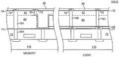
본 발명은 DRAM 시스템의 로직 부분에서만 금속층을 사용함으로써, 그리고 그것을 MIM 커패시터(50)의 바닥면(53) 이상 또는 최상면(51)의 이하에 대응하는 반도체 구조체 내의 소정의 깊이에서 사용함으로써 로직 영역 내 콘택트 높이를 감소시킨다. 그 결과, 로직 영역 내 RC 역시 감소된다. 이 프로세스에 의하면 eDRAM 시스템의 접촉 저항과 커패시턴스가 순수 로직 프로세스에 대해 기대되는 값으로 유지된다. 다시 말하면, 로직 영역 내 수직 콘택트는 임베디드 메모리에 대한 것이 없는 순수한 로직 프로세스를 사용할 때 본 발명세서 프로세스 변경을 필요로 하지 않는다. 또한, 메모리 영역 내에 M1 영역의 부존재는 메모리가 없는 로직 디바이스의 RC에 동등한 로직 영역 내에서 RC를 갖는 eDRAM 시스템과 더 작은 셀 크기가 얻어진다. 로직 영역 내에만 하나 이상의 금속층, 예컨대 M1 층(71)을 갖는 모든 실시예에서, 로직 영역 내에 생성된 비아 플러그, 예컨대 18B는 메모리 영역 내의 비아 플러그, 예컨대 18A의 높이보다 작은 높이(92)를 가질 것이며, 이에 상응하여 기생 저항 및 커패시턴스는 감소할 것이다.The present invention can be achieved by using a metal layer only in the logic portion of the DRAM system and by using it at a predetermined depth in the semiconductor structure corresponding to or below the
이제 도 2e를 참조하면, 로직 영역 내의 기생 커패시턴스가 감소된 임베디드 DRAM을 갖는 반도체 구조체(102-E)의 평면도(도 2d의 2E-2E 단면)가 본 발명의 하나 이상의 실시예와 관련하여 도시되어 있다. 3개의 S 콘택트(20C)의 둑(bank)과 3개의 D 콘택트(20D)의 둑은 거리(D1)에서 절연체(80)에 의해 분리된 사실상(de facto) 기생 커패시터의 2개의 플레이트를 의도적이지 않게 형성한다. 비교해볼 때, 트랜지스터 드레인(112B)과 소스(112A)로부터 상부 금속층으로 신호를 전달하기 위해 플러그 비아(18B, 18C)를 사용함으로써, 상기 시스템 내에는 더 적은 기생 용량성 효과가 존재하며 이것은 비아 플러그(18B, 18C)가 실질적으로 D1보다 더 큰 거리(D2)에서 더 떨어져 배치되는 것이 가능하기 때문이며, 또한 그것들이 용량성 플레이트로서 작동하는 더 작은 표면을 갖기 때문이다. 비아 플러그(18F)는 콘택트(평면도에서만 도시됨)에 의해 게이트(15)에 연결되는 금속화층(M1)(71)에 사용되고 연결된다. 도 2e에서 S(112A)와 D(112B)의 각각에 대해 오직 하나의 비아 플러그(18B, 18C)가 사용되지만, 훨씬 더 낮은 저항값을 요구하는 중요한 응용에서는, 다수의 비아 플러그가 사용되는 것이 가능하고 및/또는 더 낮은 저항값의 전도성 재료, 예컨대 구리가 플러그에 대해 사용되는 것이 가능하다. 이들 다수의 비아 플러그는 여전히 유전체층을 관통하여 더 높게 연장하는 콘택트(20D, 20D)보다 더 낮은 기생 용량성 값을 가질 수 있는데 이것은 상기 비아 플러그가 여전히 S와 D 콘택트 사이의 거리(D1)보다 서로 더 멀리 떨어진 거리(D2)로 이격되어 있기 때문이다. 대안으로, 만일 비아(18A-18C)가 텅스텐과 같은 더 높은 저항 재료로 채워지는 경우, M1 금속화층에서 회로를 라우팅함으로써 더 낮은 시스템 저항이 달성될 수 있다. 도면(102-E)이 구체적인 레이아웃을 제공하지만, 본 발명은 S와 D 거리(D1)보다 더 큰 거리(D1)을 제공하는 넓은 범위의 비아와 M1의 배치에 잘 적용된다.Referring now to FIG. 2E, a top view (2E-2E cross section in FIG. 2D) of a semiconductor structure 102-E having embedded DRAMs with reduced parasitic capacitance in a logic region is shown in connection with one or more embodiments of the present invention have. The banks of the three
본 발명의 상호접속 RC를 감소시키는 대안적인 실시예가 도 3a-3d에 도시되어 있으며, 이 도면에서 2개의 상이한 유형의 전도성 플러그를 갖는 eDRAM 시스템을 갖는 반도체 구조체(103-A ~ 103-D)가 도시되어 있다. 이 실시예는 구리 비아가 MIM 전극을 직접 접촉하는 것이 허용되지 않는 eDRAM 시스템을 지향한다.An alternative embodiment of reducing the interconnect RC of the present invention is shown in Figures 3A-3D in which a semiconductor structure 103-A-103-D having an eDRAM system with two different types of conductive plugs Respectively. This embodiment is directed to an eDRAM system in which copper vias are not allowed to directly contact the MIM electrodes.
도 3a를 참조하면 유전체층(65) 내에 배치되고 로직 영역 내의 콘택트(20C, 20D)와 전기적으로 연결되는 금속화층(M1)(71)을 구비한 부분적으로 완성된 반도체 구조체(103-A)가 도시되어 있다. 그 위에는 유전체층(80)이 배치된다. MIM 커패시터(50)는 도 2c에 대해 설명된 프로세스에 따라 제조된다. 결과적으로 얻어진 구조체에서, 금속화층(M1)(71)은 MIM 커패시터(50)의 최상면(51)과 바닥면(53) 사이의 위치에 대응하는, 기판(110) 위의 레벨에 효과적으로 위치된다.3A, a partially completed semiconductor structure 103-A having a metallization layer (M1) 71 disposed in a
이제 도 3b를 참조하면, 유전체층(82)이 유전체층(80) 위에 퇴적되고 또한 커패시터(50)의 공동을 채우며, 상기 소정의 유전체층의 두께를 증가시킨다. MIM 커패시터(50)의 상부 커패시터 플레이트(48)까지 아래로 비아(22)를 선택적으로 에칭하기 위해 유전체층(82) 위에 마스크(도시되지 않음)가 배치된다. 비아(22)는 그 다음에 본 발명에서 텅스텐으로 채워진다.Referring now to FIG. 3B, a
도 3c에 도시된 바와 같이, 마스크(52)는 비아(18A-18C)가 생성되는 영역을 한정하기 위해 비아(22)와 유전체층(82) 위에 배치된다. 비아(18A)는 유전체층(82, 80)과 에칭-방지층(77)을 통과하여 에칭되어 콘택트(20A)에 도달한다. 비아(18B, 18C)는 유전체층(80, 82)과 유전체층(68)을 통과하여 에칭되어 금속화층(M1)(71)에 도달한다. 비아(18A-18C)가 생성된 후 마스크(52)는 제거된다. 그 다음 비아(18A-18C)는 예컨대 텅스텐과 같은 전도성 재료로 채워진다.3C, mask 52 is disposed over via 22 and
이제 도 3d를 참조하면, 추후의 프로세스 작업에서 제어된 에칭을 제공하기 위해 에칭-방지층(78)이 유전체층(82)과 비아 플러그(18A-18C, 22) 위에 제공된다. 그 다음에 에칭-방지층(78) 위에 유전체층(88)이 제공되고, 그 다음 제2 금속화층(M2)(72)을 위한 홈통(도시되지 않음)을 형성하기 위해 패터닝된다. 그 다음, 홈통(도시되지 않음)은 텅스텐보다 작은 저항값을 갖는 전도성 재료, 예컨대 구리로 채워진다. 대안이 실시예에서, 비아(18A-18C)와 금속화층(M2)(72)은 유전체층들과 전술한 에칭-방지층을 관통하여 에칭될 수 있다. 그 다음 금속화층 상호접속부(M2)(72)과 비아(18A-18C)는 듀얼 다마신 프로세스를 사용하여 채워질 수 있다. 그 결과 얻어진 구조체는 다른 임베디드 DRAM 시스템과 비교하여 감소된 상호접속 저항과 감소된 커패시턴스 모두를 갖는다. 원한다면 더욱 복합적인 상호접속부를 형성하기 위해 추가의 금속층이 제공될 수 있다.Referring now to FIG. 3D, an etch-
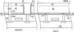
이제 도 4를 참조하면, 본 발명의 제 4 실시예에 있어서, MIM 커패시터의 최상면과 바닥면 사이의 위치에 대응하는 층에 위치한 메모리 영역 내에 제1 금속층을 구비한 임베디드 DRAM 시스템을 갖는 반도체 구조체(104)를 형성하는 프로세스 흐름의 일 부분의 단면도가 도시되어 있다. 반도체 구조체(104)는 도 2c에서 MIM 커패시터(50)의 최상면(51)과 바닥면(53) 사이의 메모리 영역에 위치되고 콘택트(20A)를 통해 드레인(111A)에 연결된 금속층(M1) 상호접속부(71)가 추가된 것에 직접 대응한다. 주목할 것은, 도 3d의 18A와 유사한 비아가 도 4의 메모리 섹션에서는 사용되지 않는 것이며, 이것은 콘택트(20A) 위의 M1(71)이 비트 라인을 위해 라우팅을 완성하기 때문이다. 상응하는 조건을 갖는 비아와 플러그에 대한 후속적인 처리 작업은 도 2d, 3c, 3d 또는 5b-5c에 의한다.4, in a fourth embodiment of the present invention, a semiconductor structure having an embedded DRAM system having a first metal layer in a memory region located in a layer corresponding to a position between a top surface and a bottom surface of the MIM capacitor Sectional view of a portion of a process flow forming a < / RTI > The
메모리 영역에서 금속층(M1) 상호접속부(71)를 사용하는 것이 메모리 셀 내의 기생 커패시턴스를 감소시키지만, 콘택트로부터 상부 금속층에 도달하기 위해 더 적은 비아가 요구되기 때문에, 그리고 상기 비아는 상기 소스 및 드레인이 서로 이격될 수 있는 것보다 더 떨어져서 이격될 수 있기 때문에, 고려해야 할 다른 트레이드오프가 존재한다. 만일 금속층(M1)이 MIM 커패시터(50)의 바닥면(53) 이상 및 최상면(51) 이하의 층 위치에서 메모리 영역 내에 위치된다면, 금속 상호접속부(71)와 커패시터(50) 사이의 최소 여유 거리(minimum clearance distance)(55)는 신호 분리를 위해 사용된다. 이 여유는 메모리 셀의 전체적인 폭을 증가시킬 것이고 아마도 덜 바람직하지만 설명된 층 위치에서 메모리 영역 내의 금속층을 이용하는 다른 트레이드오프를 생성할 것이다. 이러한 이유로, 대안적인 실시예는 여기서 MIM 커패시터(50)의 최상면과 바닥면 사이의 층 위치에서 상기 메모리 영역 내의 금속층을 회피한다.Although use of the metal layer (M1)
이제 도 5a - 5c를 참조하면, 본 발명의 제 5 실시예에 있어서, 상이한 순서의 비아 형성에 의해 MIM 커패시터를 갖는 임베디드 DRAM 시스템을 형성하는 프로세스 흐름의 단면도가 도시되어 있다. 도 5a의 부분적으로 완성된 반도체 구조체(105-A)는 M1 제1 금속층(71)을 형성하는 종래의 프로세스를 포함하는 도 2a-2c에 대해 설명된 프로세스를 따라서 제조된다. 에칭-방지층(68)과 유전체층(65)은 비아(18A)의 단순화된 에칭을 위해 유전체층(80)을 형성하기 전에 제거되는 것이 가능하지만, 도면은 MIM 커패시터(50)의 형성을 위해 필요한 경우를 제외하고는 메모리 영역 내에 에칭-방지층(68)과 유전체층(65)을 유지한다. MIM 커패시터(50)를 형성하기 위해, 유전체층(80, 65)과 에칭-방지층(68, 77)이 에칭되고 MIM 커패시터가 도 2c에 도시된 바와 같이 그 안에 형성된다. MIM 커패시터(50)의 완성 후, 그 다음 제2 유전체층(82)이 도 2c에 도시된 바와 같이 형성된다. 도 5b에서, 메모리 영역 내에 V1M 비아(18A)를 형성하기 위해 유전체층(82) 위에 마스크(도시되지 않음)가 배치되며, 이것은 에칭-방지층(68, 77)을 침투하여 콘택트(20A)에 도달한다. 비아(18A)는 그 다음 텅스텐과 같은 전도성 재료로 채워지며, 이것은 도 2d와 비교하여 비아 높이(91)에 의해 증명된 바와 같이, 비아(18A)와 같은 깊은 비아에 대해 유리한 충전 특성을 갖는다.Referring now to Figures 5A-5C, in a fifth embodiment of the present invention, a cross-sectional view of a process flow for forming an embedded DRAM system with MIM capacitors by different order of via formation is shown. The partially completed semiconductor structure 105-A of FIG. 5A is fabricated following the process described for FIGS. 2A-2C, including a conventional process of forming the M1
도 5c에서, 제2 유전체층(82) 위에 에칭-방지층(78)이 제공되며, 이것은 차례로 제 3 유전체층(88)에 의해 피복된다. 그 다음, 금속화 영역(M2) 상호접속부(72)를 위한 홈통(도시되지 않음)을 생성하기 위해 패터닝된다. 마스크(도시되지 않음)가 유전체층(88) 위에 배치되고 MIM 커패시터(50)에의 상호접속 비아(22)를 동시에 생성하고, 또한 비아(18B, 18C)를 생성하기 위해 패터닝되며, 비아 깊이의 차이는 비아(18A)에서와 같이 격렬하지 않다. 이후, 금속화 영역(M2) 상호접속부(72) 및 비아(22, 18B, 18C)를 위한 홈통이 듀얼 다마신 프로세스를 사용하여 예컨대 구리와 같은 전도성 재료로 동시에 채워진다.In Fig. 5c, an etch-
이제 도 6a 및 6b를 참조하면, 본 발명의 제 6 실시예에 있어서, MIM 커패시터의 최상면과 바닥면 사이에 위치된 로직 영역에 다수의 금속층을 갖는 임베디드 DRAM을 형성하는 프로세스 흐름의 단면도가 도시되어 있다. 도 6a의 부분적으로 완성된 반도체 구조체(106-A)는, 유전체층(65)에 M1 제1 금속층(71)을 형성하는 종래의 프로세스를 포함하여, 도 2a 및 2b에 대해 설명된 프로세스에 따라 제조되며, 유전체층(65) 위에는 제2 에칭-방지층(68)이 형성되고 다음에 제1 유전체층(89)이 배치된다. 그 다음, 유전체층(89) 위에는 에칭-방지층(79)이 배치되고, 이것은 그 다음에 그 위의 유전체층(83)을 노출시키기 위해 처리된다. 유전체층(83)은 금속화 영역(Mx1) 상호접속부(73)를 위한 홈통(도시되지 않음)을 형성하기 위해 에칭된다. 마스크(도시되지 않음)가 유전체층(83) 위에 배치되고 중간 V1L 비아(18D)를 형성하기 위해 패터닝되며, 이것은 그 다음에 텅스텐과 같은 전도성 재료로 채워진다. 금속화 영역(Mx1) 상호접속부(73)도 또한 그 다음에 전도성 재료로 채워진다. 일 실시예에서, 금속화 영역(Mx1) 상호접속부(73)와 비아(18D)는 듀얼 다마신 프로세스를 사용하여 구리 또는 구리 합금으로 채워진다.Referring now to Figures 6a and 6b, a cross-sectional view of a process flow for forming an embedded DRAM having a plurality of metal layers in a logic region positioned between a top surface and a bottom surface of a MIM capacitor is shown in a sixth embodiment of the present invention have. The partially completed semiconductor structure 106-A of FIG. 6A is fabricated according to the process described for FIGS. 2A and 2B, including a conventional process of forming the M1
유전체층(83) 위에 에칭-방지층(81)이 배치된 후 제2 유전체층(80)이 배치된다. 여분의 에칭-방지 층들이 있음에도 불구하고, 도 2c에서 설명된 프로세스와 유사한 프로세스로, 콘택트(20B)에 도달하기 위해 유전체층(80), 에칭-방지층(81), 유전체층(83), 에칭-방지층(79), 유전체층(89), 에칭-방지층(68), 유전체층(65), 및 마지막으로 에칭-방지층(77)을 관통하여 에칭한 후 MIM 커패시터(50)가 유전체층(80)에 형성된다. 그 다음 MIM 커패시터(50)의 공동(70)(도 1a에 도시됨)을 채워서 유전체층(8) 위로 그리고 MIM 커패시터(50)의 최상면(51) 위로 올라오도록 층(82)이 형성된다.A
도 6a는 단지 제1 금속층(M1)(71), 하나의 중간 금속층(Mx1)(73), 및 상부 금속층에 도달하기 위해 비아 및 플러그를 이용하는 단 하나의 콘택트(20D)를 도시한다. 그러나 본 발명은, 소정의 회로를 위한 장소와 루트에 의해 지시된 바와 같이, 상부 금속층에 도달하기 위해 로직 영역 내의 트랜지스터 소스 및/또는 드레인을 위한 적절한 콘택트를 연결하기 위해 MIM 커패시터(50)의 최상면(51)과 바닥면(53) 사이의 레벨에 대응하는 높이에서 구조체는 층에 배치된 비아 및/또는 금속층의 임의의 양 및 조합을 사용하는데 아주 적합하다.Figure 6A shows only a first metal layer (M1) 71, one intermediate metal layer (Mxl) 73, and a
이제 도 6b를 참조하면, 콘택트(20A)까지 도달하기 위해 제2 유전체층(82, 80), 에칭-방지층(81), 유전체층(83), 에칭-방지층(79), 제1 유전체응(89), 에칭-방지층(68), 유전체층(65), 에칭-방지층(77), 및 마지막으로 유전체층(75)을 통과하여 Vx1M 비아(18A)를 선택적으로 에칭하기 위해 유전체층(82) 위에 마스크(도시되지 않음)가 배치된다. 마스크의 제거 후, 그리고 차후 프로세스 단계에서 제어된 에칭을 제공하기 위해, 제2 유전체층(82) 위에 에칭-방지층(85)이 제공되고 그 다음 제 3 유전체층(87)이 형성된다. 그 다음, 유전체층(87)과 에칭-방지층(85) 내에 금속화 영역(Mx2) 상호접속부(72)를 위한 홈통(도시되지 않음)을 생성하기 위해 층(87)이 패터닝되며, 여기서 x2 = x1 + 1. 유전체층(87) 위에 마스크(도시되지 않음)가 배치되고, MIM 커패시터(50)의 상부 커패시터 플레이트(48)에 도달하는 상호접속 비아(22); 금속화층(Mx1)(73)에 도달하는 비아(Vx1L)(18E)를 동시에 형성하도록 패터닝된다. 비아(22)는 MIM 커패시터(50)의 상부 커패시터 플레이트(48)에 도달하도록 유전체층(82)의 일부만을 관통하여 에칭된다. 비아(Vx1L)(18E)는 유전체층(82, 80) 2개를 관통 에칭하여 형성된다. 금속화 영역(Mx2)(72)을 위한 홈통 외에 2개의 비아(22, 18E)는 구리 또는 구리 기반 합금으로 듀얼 다마신 프로세스에 의해 채워진다. 그 결과 얻어진 구조체는 다른 임베디드 DRAM과 비교하여 감소된 상호접속 저항과 감소된 커패시턴스 모두를 갖는다.Referring now to FIG. 6B, a
본 발명의 실시예는 단지 예시적인 것이고 어떤 식으로든 본 발명을 한정하려는 것은 아니다. 여기서 설명된 방법 및 작업들은 여기서 설명된 전형적인 것들과 상이한 조합과 변경으로, 예컨대 상이한 세트 및/또는 순서로 실행될 수 있다. 따라서, 실질적으로 동일한 기능, 방법 및 결과를 얻기 위해, 하나 이상의 추가의 새로운 작업들이 기존의 작업에 추가되거나, 하나 이상의 작업들이 주어진 응용에 따라 생략되거나 제거될 수 있다. 마찬가지로, 여기서 설명된 구조체는 및 장치의 특징 및 부분들은 실질적으로 동일한 기능, 방법 및 결과를 얻기 위해 연결될 수 있다.The embodiments of the invention are illustrative only and are not intended to limit the invention in any way. The methods and operations described herein may be implemented in different combinations and variations, e.g., in different sets and / or sequences, than those described herein. Thus, in order to obtain substantially the same functions, methods and results, one or more additional new tasks may be added to the existing task, or one or more tasks may be omitted or eliminated depending on the given application. Likewise, the structures described herein and the features and parts of the apparatus may be connected to obtain substantially the same functions, methods, and results.
예를 들면, 도시된 로직 구조체는 모든 로직 영역에서 반복될 필요가 없다. IC 다비이스 내의 일부 로직 구조체는 더 높은 수준의 금속이 상호접속부를 위해 필요한지 여부에 따라 도시된 것보다 더 적거나 많은 비아를 가질 수 있다. 본 발명은 구조체와 제1 금속층 사이에 삽입된 MIM 커패시터를 갖는 eDRAM으로서 설명되었지만, 본 발명의 프로세스는 메모리 영역 내 2개의 금속층 사이에 MIM 커패시터를 삽입함으로써 실행될 수도 있다. 개시된 방법을 사용하여 현재 개시된 것과 같은 임의의 수의 메모리 디바이스, 예컨대 어레이와 로직 디바이스 장치들은, 추가의 작업 및 마스크 및 다른 재료가 요구되기는 하지만, 다른 기능 블록 및 기존 디바이스 및 프로세스에 추가하여, 주어진 ICIintegrated circuit), SOC(system-on-chip), WSI(wafer-scale integration)에 집적될 수 있다. 본 실시예에서 구체적인 재료 및 프로세스가 설명되었지만, 본 발명은 반도체 구조체에, 예컨대 MIM 커패시터의 최상면과 바닥면 사이의 위치에 대응하는 층에, 배치된 금속화 상호접속부 및 비아를 제공하기 위해 임의의 적절한 프로세스 기술과 작업을 사용하기에 아주 적합하다. 예를 들면, 콘택트에 M1 금속화층을 연결시키기 위해 단일의 다마신 프로세스가 사용될 수 있다. 마찬가지로, 여기서는 특정 층과 비아를 위해 텅스텐과 구리가 사용되었지만, 본 발명은 이것들 외에 알루미늄과 같은 다른 전도체와, 제조 또는 주물 공장에 의해 지시된 것과 같은, 주어진 프로세스 또는 기술에 필요한, 다른 퇴적, 에칭, 제거 또는 화학-기계적 폴리싱(CMP)의 사용에 아주 적합하다.For example, the illustrated logic structure need not be repeated in all logic regions. Some logic structures in the IC device may have fewer or more vias than shown, depending on whether a higher level of metal is needed for the interconnect. While the present invention has been described as an eDRAM having a MIM capacitor interposed between a structure and a first metal layer, the process of the present invention may also be implemented by inserting an MIM capacitor between two metal layers in a memory region. Any number of memory devices, such as arrays and logic device devices, such as those currently disclosed using the disclosed methodology, in addition to other functional blocks and existing devices and processes, require additional tasks and masks and other materials, ICI integrated circuit, system-on-chip (SOC), and wafer-scale integration (WSI). Although specific materials and processes have been described in this embodiment, the present invention is also applicable to any semiconductor structure, such as, for example, any of a number of metal interconnects and vias disposed in a layer corresponding to a location between a top surface and a bottom surface of a MIM capacitor, It is well suited for use with appropriate process skills and work. For example, a single damascene process can be used to connect the M1 metallization layer to the contacts. Likewise, although tungsten and copper are used herein for particular layers and vias, the present invention contemplates that other conductors, such as aluminum, and other conductors, such as those directed by a fabrication or foundry, , Removal or chemical-mechanical polishing (CMP).
본 발명의 다른 특징들은 첨부한 도면과 상세한 설명으로부터 명백할 것이다. 따라서, 명세서와 도면은 한정적인 의미에서가 아니라 예시적인 것으로 취급되어야 한다. 당업자는 전술한 실시예의 다양한 변형이 있을 수 있음을 용이하게 인식할 수 있을 것이다. 결론적으로, 본 발명은 이하에서 제시되는 청구항들에 의해 한정된다.Other features of the invention will be apparent from the accompanying drawings and detailed description. Accordingly, the specification and drawings are to be regarded in an illustrative rather than a restrictive sense. Those skilled in the art will readily recognize that there can be many variations of the embodiments described above. In conclusion, the invention is defined by the claims set forth below.
42: 하부 커패시터 플레이트44, 75, 77, 80: 절연층
48: 상부 커패시터 플레이트110: 기판
111A: 드레인 영역111B: 소스 영역
20A-20D: 콘택트50: MIM 커패시터42:
48: upper capacitor plate 110: substrate
111A: drain
20A-20D: contact 50: MIM capacitor
Claims (29)
Translated fromKorean임베디드 RAM을 갖는 메모리 영역;
상기 메모리 영역에 연결된 로직 영역;
상기 메모리 영역 내에 배치된 MIM(metal-insulator-metal) 커패시터;
상기 MIM 커패시터의 최상면과 바닥면 사이에 위치된 금속 라인을 위한 하나 이상의 금속층; 및
제1 금속층의 부분을 그 위에 배치된 또 다른 금속층의 부분에 연결하기 위해 상기 로직 영역 내에 배치된 하나 이상의 비아 플러그를 포함하고,
상기 하나 이상의 비아 플러그는 주어진 트랜지스터의 소스 콘택트 및 드레인 콘택트 사이의 거리보다 서로 더 떨어져 배치되는 것을 특징으로 하는 반도체 구조체.1. A semiconductor structure provided on a substrate,
A memory area having embedded RAM;
A logic region coupled to the memory region;
A metal-insulator-metal (MIM) capacitor disposed in the memory region;
One or more metal layers for metal lines located between the top and bottom surfaces of the MIM capacitor; And
At least one via plug disposed within the logic region for coupling a portion of the first metal layer to a portion of another metal layer disposed thereon,
Wherein the one or more via plugs are disposed further apart than a distance between a source contact and a drain contact of a given transistor.
금속 라인을 위한 상기 하나 이상의 금속층은 상기 반도체 구조체의 로직 영역 내에만 위치되는 것을 특징으로 하는 반도체 구조체.The method according to claim 1,
Wherein the at least one metal layer for a metal line is located only in a logic region of the semiconductor structure.
상기 로직 영역 내에만 배치된 금속 라인을 위한 상기 하나 이상의 금속층은 상기 MIM 커패시터의 최상부와 상기 기판 사이에 위치되는 것을 특징으로 하는 반도체 구조체.3. The method of claim 2,
Wherein the at least one metal layer for a metal line disposed only within the logic region is located between the top of the MIM capacitor and the substrate.
금속 라인을 위한 상기 하나 이상의 금속층은 상기 로직 영역과 상기 메모리 영역의 드레인 부분 내에만 위치되어 상기 로직 영역보다 상기 메모리 영역 내에 더 적은 개수의 금속층이 존재하는 것을 특징으로 하는 반도체 구조체.The method according to claim 1,
Wherein the at least one metal layer for the metal line is located only in the logic region and the drain portion of the memory region, such that a lesser number of metal layers are present in the memory region than the logic region.
상기 로직 영역은,
각각 소스, 드레인, 및 하나 이상의 콘택트를 갖고 상기 로직 영역 내에만 위치된 하나 이상의 트랜지스터를 더 포함하고,
상기 하나 이상의 트랜지스터는 상기 소스와 드레인 각각에 대해 상기 로직 영역 내에만 배치된 금속 라인을 위한 상기 하나 이상의 금속층의 제1 금속층의 각 부분에 상기 소스를 연결하고 상기 드레인을 연결하며,
상기 로직 영역 내의 하나 이상의 트랜지스터의 상기 하나 이상의 콘택트의 최상면은 상기 메모리 영역 내의 상기 MIM 커패시터의 높이와 같거나 더 낮은 높이에 배치되는 것을 특징으로 하는 반도체 구조체.The method according to claim 1,
Wherein the logic region comprises:
Further comprising one or more transistors each having a source, a drain, and one or more contacts and located only in the logic region,
Wherein the at least one transistor connects the source to each portion of the first metal layer of the one or more metal layers for a metal line disposed only in the logic region for each of the source and drain and connects the drain,
Wherein the top surface of the one or more contacts of the one or more transistors in the logic region is located at a height equal to or lower than a height of the MIM capacitor in the memory region.
상기 로직 영역 내의 하나 이상의 트랜지스터는 드레인 및 소스를 갖고,
상기 드레인은 주어진 수량의 비아 플러그 또는 콘택트 플러그에 연결되며,
상기 소스는 주어진 수량의 비아 플러그 또는 콘택트 플러그에 연결되고,
상기 드레인을 위한 비아 플러그 또는 콘택트 플러그의 상기 수량은 상기 소스를 위한 비아 플러그 또는 콘택트 플러그의 상기 수량과 같지 않은 것을 특징으로 하는 반도체 구조체.The method according to claim 1,
Wherein at least one transistor in the logic region has a drain and a source,
The drain is connected to a given number of via plugs or contact plugs,
The source is connected to a given number of via plugs or contact plugs,
Wherein the quantity of the via plug or contact plug for the drain is not equal to the quantity of the via plug or contact plug for the source.
상기 MIM 커패시터 위에 배치된 상기 메모리 영역의 제1 금속층;
각각 소스, 드레인, 및 하나 이상의 콘택트를 갖고 상기 메모리 영역 내에만 위치된 하나 이상의 트랜지스터; 및
상기 메모리 영역 내에만 위치된 상기 하나 이상의 트랜지스터의 하나 이상의 콘택트에 상기 메모리 영역 내의 상기 제1 금속층을 연결하는, 상기 메모리 영역 내에 배치된 하나 이상의 비아 플러그(via plug)를 더 포함하고,
상기 하나 이상의 트랜지스터는 상기 소스와 드레인 각각에 대해 상기 소스와 상기 드레인을 각각 상기 메모리 영역의 상기 제1 금속층에 연결하고,
상기 메모리 영역 내의 주어진 트랜지스터의 소스 및 드레인 중 둘 다는 아니고 어느 하나가 각각의 하나 이상의 콘택트에 의해 상기 MIM 커패시터에 연결되는 것을 특징으로 하는 반도체 구조체.The method according to claim 1,
A first metal layer of the memory region disposed over the MIM capacitor;
One or more transistors each having a source, a drain, and one or more contacts and located only in the memory region; And
Further comprising: at least one via plug disposed within the memory region for connecting the first metal layer within the memory region to at least one contact of the at least one transistor located only within the memory region,
The at least one transistor coupling the source and the drain to the first metal layer of the memory region for each of the source and drain,
Wherein one of the source and the drain of a given transistor in the memory region is connected to the MIM capacitor by a respective one or more contacts.
상기 메모리 영역 내에 또는 상기 로직 영역 내에 배치된 하나 이상의 비아 플러그는 텅스텐, 구리 또는 이것들의 조합인 것을 특징으로 하는 반도체 구조체.The method according to claim 1,
Wherein the at least one via plug disposed within or within the memory region is tungsten, copper, or a combination thereof.
상기 메모리 영역 및 상기 로직 영역 둘 다의 위에 배치되고 각각의 상기 메모리 영역과 상기 로직 영역 내의 하나 이상의 트랜지스터에 연결된 금속층을 더 포함하고,
상기 메모리 영역과 상기 로직 영역 둘 다의 위에 배치된 상기 금속층은 상기 메모리 영역을 위한 제1 금속층이고 상기 로직 영역을 위한 제2 또는 그 이상의 금속층인 것을 특징으로 하는 반도체 구조체.The method according to claim 1,
Further comprising a metal layer disposed over both the memory region and the logic region and connected to one or more transistors in each of the memory region and the logic region,
Wherein the metal layer disposed on both the memory region and the logic region is a first metal layer for the memory region and a second or more metal layer for the logic region.
상기 로직 영역 내의 트랜지스터를 위한 콘택트를 상기 로직 영역 내의 제2 금속층에 연결하는, 상기 로직 영역 내의 비아 플러그는 상기 메모리 영역 내의 제1 금속층으로부터 상기 메모리 영역 내의 트랜지스터를 위한 콘택트까지의 거리보다 작은 높이를 갖는 것을 특징으로 하는 반도체 구조체.The method according to claim 1,
A via plug in the logic region connecting a contact for a transistor in the logic region to a second metal layer in the logic region has a height less than a distance from a first metal layer in the memory region to a contact for a transistor in the memory region ≪ / RTI >
상기 로직 영역 내의 하나 이상의 트랜지스터 각각은 임베디드 RAM를 갖지 않은 로직 회로에서 사용된 트랜지스터에 등가의 기생 커패시턴스를 갖는 것을 특징으로 하는 반도체 구조체.The method according to claim 1,
Wherein each of the one or more transistors in the logic region has an equivalent parasitic capacitance to a transistor used in a logic circuit having no embedded RAM.
소스 및 드레인을 갖는 트랜지스터를 로직 영역 내에 형성하는 단계;
소스 및 드레인을 갖는 트랜지스터를 메모리 영역 내에 형성하는 단계;
유전체층을 형성하는 단계;
상기 로직 영역 내의 트랜지스터와 상기 메모리 영역 내의 트랜지스터의 소스 및 드레인을 위해 상기 유전체층 내에 하나 이상의 콘택트를 형성하는 단계;
상기 메모리 영역 내에 배치된 상기 트랜지스터에 연결되는, 상기 유전체층 내에 MIM 커패시터를 형성하는 단계;
상기 MIM 커패시터의 최상면 및 바닥면 사이의 위치에서 상기 유전체층 내에 금속 라인을 위한, 상기 로직 영역 내에 하나 이상의 금속층을 형성하는 단계;
상기 메모리 영역 내에 하나 이상의 비아 플러그를 형성하는 단계; 및
상기 로직 영역 내의 제1 금속층의 부분을 그 위에 배치된 상기 로직 영역 내의 다른 금속층의 부분에 연결하기 위해 상기 로직 영역 내에 하나 이상의 비아 플러그를 형성하는 단계를 포함하고,
상기 로직 영역 내의 상기 하나 이상의 비아 플러그는 상기 로직 영역 내에 주어진 트랜지스터의 소스 및 드레인에 각각 대응하는 상기 로직 영역 내의 하나 이상의 콘택트보다 서로 더 떨어져 배치되는 것을 특징으로 하는 반도체 구조체 형성 방법.A method of forming a semiconductor structure,
Forming a transistor having a source and a drain in a logic region;
Forming a transistor having a source and a drain in a memory region;
Forming a dielectric layer;
Forming at least one contact in the dielectric layer for a transistor in the logic region and a source and a drain of a transistor in the memory region;
Forming an MIM capacitor in the dielectric layer, the MIM capacitor being connected to the transistor disposed in the memory region;
Forming at least one metal layer in the logic region for a metal line in the dielectric layer at a location between the top and bottom surfaces of the MIM capacitor;
Forming at least one via plug in the memory region; And
Forming at least one via plug in the logic region to connect a portion of the first metal layer within the logic region to a portion of another metal layer within the logic region disposed thereon,
Wherein the one or more via plugs in the logic region are disposed further apart than one or more contacts in the logic region corresponding to a source and a drain of a given transistor in the logic region, respectively.
상기 반도체 구조체 내에 형성된 금속 라인을 위한 상기 하나 이상의 금속층은 상기 반도체 구조체의 로직 영역 내에만 위치되는 것을 특징으로 하는 반도체 구조체 형성 방법.13. The method of claim 12,
Wherein the at least one metal layer for a metal line formed in the semiconductor structure is located only in a logic region of the semiconductor structure.
상기 로직 영역 내에만 위치된 금속 라인을 위한 상기 하나 이상의 금속층의 상기 제1 금속층은 상기 로직 영역 내에 배치된 트랜지스터의 드레인의 하나 이상의 콘택트 및 소스의 하나 이상의 콘택트에 전기적으로 연결되는 것을 특징으로 하는 반도체 구조체 형성 방법.14. The method of claim 13,
Wherein the first metal layer of the at least one metal layer for a metal line located only within the logic region is electrically connected to at least one contact of the drain and at least one contact of the drain of the transistor disposed in the logic region. ≪ / RTI >
상기 반도체 구조체 내에 형성된 금속 라인을 위한 상기 하나 이상의 금속층은 상기 반도체 구조체의 메모리 영역의 드레인 부분 내 및 상기 로직 영역 내에만 위치되어 상기 로직 영역보다 상기 메모리 영역 내에 더 적은 개수의 금속층이 존재하는 것을 특징으로 하는 반도체 구조체 형성 방법.13. The method of claim 12,
Characterized in that the one or more metal layers for the metal lines formed in the semiconductor structure are located only in the drain portion and in the logic region of the memory structure of the semiconductor structure so that fewer metal layers are present in the memory region than in the logic structure To form a semiconductor structure.
금속 라인을 위한 상기 하나 이상의 금속층은 기판과 상기 MIM 커패시터의 최상면 사이에 위치되는 것을 특징으로 하는 반도체 구조체 형성 방법.13. The method of claim 12,
Wherein said at least one metal layer for a metal line is positioned between a substrate and an uppermost surface of said MIM capacitor.
상기 로직 영역 내의 하나 이상의 트랜지스터는 드레인 및 소스를 갖고,
상기 드레인은 주어진 수량의 비아 플러그 또는 콘택트 플러그에 연결되며,
상기 소스는 주어진 수량의 비아 플러그 또는 콘택트 플러그에 연결되고,
상기 드레인을 위한 비아 플러그 또는 콘택트 플러그의 상기 수량은 상기 소스를 위한 비아 플러그 또는 콘택트 플러그의 상기 수량과 같지 않은 것을 특징으로 하는 반도체 구조체 형성 방법.13. The method of claim 12,
Wherein at least one transistor in the logic region has a drain and a source,
The drain is connected to a given number of via plugs or contact plugs,
The source is connected to a given number of via plugs or contact plugs,
Wherein the quantity of the via plug or the contact plug for the drain is not the same as the quantity of the via plug or the contact plug for the source.
상기 MIM 커패시터 위에 배치된 상기 메모리 영역의 제1 금속층을 형성하는 단계; 및
각각 소스, 드레인, 및 하나 이상의 콘택트를 갖고 상기 메모리 영역 내에만 위치된 하나 이상의 트랜지스터를 형성하는 단계;를 더 포함하고,
상기 하나 이상의 트랜지스터를 형성하는 단계에서, 상기 하나 이상의 트랜지스터는 상기 소스와 드레인 각각에 대해 상기 소스와 드레인을 각각 상기 메모리 영역의 상기 제1 금속층에 연결하고,
상기 메모리 영역 내에 배치되는 상기 하나 이상의 비아 플러그는 상기 메모리 영역 내에만 위치된 상기 하나 이상의 트랜지스터의 하나 이상의 콘택트에 상기 메모리 영역 내의 상기 제1 금속층을 연결하며,
상기 메모리 영역 내에 주어진 트랜지스터의 상기 소스 및 드레인의 둘 다가 아닌 어느 하나는 각각의 하나 이상의 콘택트에 의해 상기 MIM 커패시터에 연결되는 것을 특징으로 하는 반도체 구조체 형성 방법.13. The method of claim 12,
Forming a first metal layer of the memory region disposed over the MIM capacitor; And
Further comprising forming at least one transistor having a source, a drain, and one or more contacts and located only in the memory region,
Wherein the one or more transistors connect the source and drain to the first metal layer of the memory region, respectively, for the source and drain,
Wherein the at least one via plug disposed within the memory region connects the first metal layer within the memory region to at least one contact of the at least one transistor located only within the memory region,
Wherein either one of the source and the drain of a given transistor in the memory region is connected to the MIM capacitor by a respective one or more contacts.
상기 메모리 영역 내에 또는 상기 로직 영역 내에 배치된 상기 하나 이상의 비아 플러그는 텅스텐, 구리 또는 이들의 조합인 것을 특징으로 하는 반도체 구조체 형성 방법.13. The method of claim 12,
Wherein the at least one via plug disposed within the memory region or within the logic region is tungsten, copper, or a combination thereof.
각각의 상기 메모리 영역과 상기 로직 영역 내의 하나 이상의 트랜지스터에 연결된, 상기 메모리 영역 및 상기 로직 영역 둘 다의 위에 배치된 금속층을 형성하는 단계를 더 포함하고,
상기 메모리 영역과 상기 로직 영역 둘 다의 위에 배치된 상기 금속층은 상기 메모리 영역을 위한 제1 금속층이고 상기 로직 영역을 위한 제2 또는 그 이상의 금속층인 것을 특징으로 하는 반도체 구조체 형성 방법.13. The method of claim 12,
Further comprising forming a metal layer disposed over both the memory region and the logic region, each memory region being connected to one or more transistors in the logic region,
Wherein the metal layer disposed on both the memory region and the logic region is a first metal layer for the memory region and a second or more metal layer for the logic region.
상기 로직 영역 내의 트랜지스터를 위한 콘택트를 상기 로직 영역 내의 제2 금속층에 연결하는 상기 로직 영역 내의 비아 플러그는, 상기 메모리 영역 내의 제1 금속층으로부터 상기 메모리 영역 내의 트랜지스터를 위한 콘택트까지의 거리보다 작은 높이를 갖는 것을 특징으로 하는 반도체 구조체 형성 방법.13. The method of claim 12,
A via plug in the logic region connecting a contact for a transistor in the logic region to a second metal layer in the logic region has a height less than a distance from a first metal layer in the memory region to a contact for a transistor in the memory region And forming the semiconductor structure.
상기 메모리 영역 내의 상기 MIM 커패시터의 일부를 노출시키기 위해 상기 유전체층 내에 제1 비아를 형성하는 단계;
제1 전도성 재료로 상기 제1 비아 내에 제1 플러그를 생성하는 단계;
상기 제1 플러그를 마스킹하는 단계;
상기 메모리 영역 내의 상기 트랜지스터의 상기 드레인과 상기 로직 영역 내의 상기 트랜지스터의 상기 드레인 및 상기 소스의 상기 하나 이상의 콘택트 모두를 노출시키기 위해 상기 유전체층 내에 한 세트의 비아를 형성하는 단계; 및
제2 전도성 재료로 상기 한 세트의 비아를 위한 한 세트의 플러그를 생성하는 단계를 더 포함하고,
상기 제2 전도성 재료는 상기 제1 전도성 재료보다 낮은 저항을 갖는 것을 특징으로 하는 반도체 구조체 형성 방법.13. The method of claim 12,
Forming a first via in the dielectric layer to expose a portion of the MIM capacitor in the memory region;
Creating a first plug in the first via with a first conductive material;
Masking the first plug;
Forming a set of vias in the dielectric layer to expose both the drain of the transistor in the memory region and the drain of the transistor in the logic region and the one or more contacts of the source; And
Further comprising the step of creating a set of plugs for said set of vias with a second conductive material,
Wherein the second conductive material has a lower resistance than the first conductive material.
상기 메모리 영역 내의 상기 MIM 커패시터의 일부를 노출시키기 위해, 그리고 상기 메모리 영역 내의 상기 트랜지스터의 상기 드레인과 상기 로직 영역의 상기 트랜지스터의 상기 드레인 및 상기 소스의 상기 하나 이상의 콘택트 모두를 노출시키기 위해, 상기 유전체층 내에 한 세트의 비아를 형성하는 단계; 및
전도성 재료로 상기 한 세트의 비아를 위한 한 세트의 플러그를 생성하는 단계를 더 포함하는 것을 특징으로 하는 반도체 구조체 형성 방법.13. The method of claim 12,
To expose a portion of the MIM capacitor in the memory region and to expose both the drain of the transistor in the memory region and the drain of the transistor in the logic region and the one or more contacts of the source, Forming a set of vias in the substrate; And
Forming a set of plugs for said set of vias with a conductive material. ≪ RTI ID = 0.0 > 11. < / RTI >
상기 메모리 영역 내의 상기 트랜지스터의 상기 드레인의 상기 하나 이상의 콘택트 모두를 노출시키기 위해 상기 유전체층 내에 제1 비아를 형성하는 단계;
제1 전도성 재료로 상기 제1 비아 내에 제1 플러그를 생성하는 단계;
상기 제1 플러그를 마스킹하는 단계;
상기 메모리 영역 내의 상기 MIM 커패시터의 일부를 노출시키기 위해, 그리고 상기 로직 영역 내의 상기 트랜지스터의 상기 드레인 및 상기 소스의 상기 하나 이상의 콘택트 모두를 노출시키기 위해, 상기 유전체층 내에 한 세트의 비아를 형성하는 단계; 및
제2 전도성 재료로 상기 한 세트의 비아를 위한 한 세트의 플러그를 생성하는 단계를 더 포함하고,
상기 제2 전도성 재료는 상기 제1 전도성 재료보다 작은 저항을 갖는 것을 특징으로 하는 반도체 구조체 형성 방법.13. The method of claim 12,
Forming a first via in the dielectric layer to expose all of the one or more contacts of the drain of the transistor in the memory region;
Creating a first plug in the first via with a first conductive material;
Masking the first plug;
Forming a set of vias in the dielectric layer to expose a portion of the MIM capacitor in the memory region and to expose both the drain of the transistor and the one or more contacts of the source in the logic region; And
Further comprising the step of creating a set of plugs for said set of vias with a second conductive material,
Wherein the second conductive material has a lower resistivity than the first conductive material.
임베디드 RAM을 갖는 메모리 영역;
상기 메모리 영역에 연결된 로직 영역;
상기 메모리 영역 내에 배치된 MIM 커패시터; 및
상기 MIM 커패시터의 최상면과 바닥면 사이에 위치된 금속 라인을 위한 하나 이상의 금속층을 포함하고,
금속 라인을 위한 상기 하나 이상의 금속층은 상기 메모리 영역의 드레인 부분 내 및 상기 로직 영역 내에만 위치되어 상기 로직 영역보다 상기 메모리 영역 내에 더 적은 개수의 금속층이 존재하는 것을 특징으로 하는 반도체 구조체.1. A semiconductor structure provided on a substrate,
A memory area having embedded RAM;
A logic region coupled to the memory region;
A MIM capacitor disposed within the memory region; And
At least one metal layer for a metal line located between the top and bottom surfaces of the MIM capacitor,
Wherein the at least one metal layer for the metal line is located only in the drain portion and in the logic region of the memory region and a lesser number of metal layers are present in the memory region than the logic region.
상기 로직 영역 내의 하나 이상의 트랜지스터는 드레인 및 소스를 갖고,
상기 드레인은 주어진 수량의 비아 플러그 또는 콘택트 플러그에 연결되며,
상기 소스는 주어진 수량의 비아 플러그 또는 콘택트 플러그에 연결되고,
상기 드레인을 위한 비아 플러그 또는 콘택트 플러그의 상기 수량은 상기 소스를 위한 비아 플러그 또는 콘택트 플러그의 상기 수량과 같지 않은 것을 특징으로 하는 반도체 구조체.26. The method of claim 25,
Wherein at least one transistor in the logic region has a drain and a source,
The drain is connected to a given number of via plugs or contact plugs,
The source is connected to a given number of via plugs or contact plugs,
Wherein the quantity of the via plug or contact plug for the drain is not equal to the quantity of the via plug or contact plug for the source.
각각의 상기 로직 영역 및 상기 메모리 영역 내의 하나 이상의 트랜지스터에 연결되고, 상기 메모리 영역 및 상기 로직 영역의 둘 다 위에 배치된 금속층을 더 포함하고,
상기 메모리 영역 및 상기 로직 영역의 둘 다 위에 배치된 상기 금속층은 상기 메모리 영역을 위한 제1 금속층이고 상기 로직 영역을 위한 제2 또는 그 이상의 금속층인 것을 특징으로 하는 반도체 구조체.26. The method of claim 25,
Further comprising a metal layer coupled to one or more transistors in each of the logic regions and the memory region and disposed over both the memory region and the logic region,
Wherein the metal layer disposed on both the memory region and the logic region is a first metal layer for the memory region and a second or more metal layer for the logic region.
임베디드 RAM을 갖는 메모리 영역;
상기 메모리 영역에 연결된 로직 영역;
상기 메모리 영역 내에 배치된 MIM 커패시터; 및
상기 MIM 커패시터의 최상면과 바닥면 사이에 위치된 금속 라인을 위한 하나 이상의 금속층을 포함하고,
상기 로직 영역 내의 하나 이상의 트랜지스터는 드레인 및 소스를 갖고,
상기 드레인은 주어진 수량의 비아 플러그 또는 콘택트 플러그에 연결되며,
상기 소스는 주어진 수량의 비아 플러그 또는 콘택트 플러그에 연결되고,
드레인을 위한 비아 플러그 또는 콘택트 플러그의 상기 수량은 소스를 위한 비아 플러그 또는 콘택트 플러그의 상기 수량과 같지 않은 것을 특징으로 하는 반도체 구조체.1. A semiconductor structure provided on a substrate,
A memory area having embedded RAM;
A logic region coupled to the memory region;
A MIM capacitor disposed within the memory region; And
At least one metal layer for a metal line located between the top and bottom surfaces of the MIM capacitor,
Wherein at least one transistor in the logic region has a drain and a source,
The drain is connected to a given number of via plugs or contact plugs,
The source is connected to a given number of via plugs or contact plugs,
Wherein said quantity of via plugs or contact plugs for drain is not equal to said quantity of via plugs or contact plugs for the source.
각각의 상기 로직 영역 및 상기 메모리 영역 내의 하나 이상의 트랜지스터에 연결되고, 상기 메모리 영역 및 상기 로직 영역의 둘 다 위에 배치된 금속층을 더 포함하고,
상기 메모리 영역 및 상기 로직 영역의 둘 다 위에 배치된 상기 금속층은 상기 메모리 영역을 위한 제1 금속층이고 상기 로직 영역을 위한 제2 또는 그 이상의 금속층인 것을 특징으로 하는 반도체 구조체.29. The method of claim 28,
Further comprising a metal layer coupled to one or more transistors in each of the logic regions and the memory region and disposed over both the memory region and the logic region,
Wherein the metal layer disposed on both the memory region and the logic region is a first metal layer for the memory region and a second or more metal layer for the logic region.
Applications Claiming Priority (4)
| Application Number | Priority Date | Filing Date | Title |
|---|---|---|---|
| US12/804,855US8460995B2 (en) | 2010-07-30 | 2010-07-30 | Method of forming a MIM capacitor |
| US12/804,855 | 2010-07-30 | ||
| US13/191,423 | 2011-07-26 | ||
| US13/191,423US8587046B2 (en) | 2010-07-30 | 2011-07-26 | System with logic and embedded MIM capacitor |
Publications (2)
| Publication Number | Publication Date |
|---|---|
| KR20120012443A KR20120012443A (en) | 2012-02-09 |
| KR101475105B1true KR101475105B1 (en) | 2014-12-22 |
Family
ID=45525847
Family Applications (1)
| Application Number | Title | Priority Date | Filing Date |
|---|---|---|---|
| KR1020110075918AExpired - Fee RelatedKR101475105B1 (en) | 2010-07-30 | 2011-07-29 | System with logic and embedded mim capacitor |
Country Status (4)
| Country | Link |
|---|---|
| US (1) | US8587046B2 (en) |
| KR (1) | KR101475105B1 (en) |
| CN (1) | CN102403318B (en) |
| TW (1) | TWI511268B (en) |
Families Citing this family (4)
| Publication number | Priority date | Publication date | Assignee | Title |
|---|---|---|---|---|
| US9276057B2 (en)* | 2014-01-27 | 2016-03-01 | United Microelectronics Corp. | Capacitor structure and method of manufacturing the same |
| US9991331B2 (en)* | 2016-09-26 | 2018-06-05 | Micron Technology, Inc. | Apparatuses and methods for semiconductor circuit layout |
| TWI737282B (en)* | 2020-04-29 | 2021-08-21 | 力晶積成電子製造股份有限公司 | Semiconductor device and manufacturing method thereof |
| CN113921514A (en)* | 2021-09-28 | 2022-01-11 | 芯盟科技有限公司 | A test wafer, chip forming method and chip testing method |
Citations (4)
| Publication number | Priority date | Publication date | Assignee | Title |
|---|---|---|---|---|
| US6528366B1 (en)* | 2001-03-01 | 2003-03-04 | Taiwan Semiconductor Manufacturing Company | Fabrication methods of vertical metal-insulator-metal (MIM) capacitor for advanced embedded DRAM applications |
| US20030073286A1 (en)* | 2001-10-15 | 2003-04-17 | Taiwan Semiconductor Manufacturing Co., Ltd. | Novel MIM process for logic-based embedded RAM |
| US6720232B1 (en)* | 2003-04-10 | 2004-04-13 | Taiwan Semiconductor Manufacturing Company | Method of fabricating an embedded DRAM for metal-insulator-metal (MIM) capacitor structure |
| US20040173836A1 (en)* | 2003-03-07 | 2004-09-09 | Oh Jae-Hee | Semiconductor device and method of manufacturing the same |
Family Cites Families (5)
| Publication number | Priority date | Publication date | Assignee | Title |
|---|---|---|---|---|
| US6285050B1 (en)* | 1997-12-24 | 2001-09-04 | International Business Machines Corporation | Decoupling capacitor structure distributed above an integrated circuit and method for making same |
| DE10131625B4 (en)* | 2001-06-29 | 2006-06-14 | Infineon Technologies Ag | Method for producing a FeRAM memory |
| WO2003052829A1 (en)* | 2001-12-14 | 2003-06-26 | Hitachi, Ltd. | Semiconductor device and method for manufacturing the same |
| JP4744788B2 (en)* | 2003-05-22 | 2011-08-10 | ルネサスエレクトロニクス株式会社 | Manufacturing method of semiconductor device |
| US7442609B2 (en)* | 2004-09-10 | 2008-10-28 | Infineon Technologies Ag | Method of manufacturing a transistor and a method of forming a memory device with isolation trenches |
- 2011
- 2011-07-26USUS13/191,423patent/US8587046B2/enactiveActive
- 2011-07-28TWTW100126810Apatent/TWI511268B/ennot_activeIP Right Cessation
- 2011-07-29CNCN201110215267.9Apatent/CN102403318B/ennot_activeExpired - Fee Related
- 2011-07-29KRKR1020110075918Apatent/KR101475105B1/ennot_activeExpired - Fee Related
Patent Citations (4)
| Publication number | Priority date | Publication date | Assignee | Title |
|---|---|---|---|---|
| US6528366B1 (en)* | 2001-03-01 | 2003-03-04 | Taiwan Semiconductor Manufacturing Company | Fabrication methods of vertical metal-insulator-metal (MIM) capacitor for advanced embedded DRAM applications |
| US20030073286A1 (en)* | 2001-10-15 | 2003-04-17 | Taiwan Semiconductor Manufacturing Co., Ltd. | Novel MIM process for logic-based embedded RAM |
| US20040173836A1 (en)* | 2003-03-07 | 2004-09-09 | Oh Jae-Hee | Semiconductor device and method of manufacturing the same |
| US6720232B1 (en)* | 2003-04-10 | 2004-04-13 | Taiwan Semiconductor Manufacturing Company | Method of fabricating an embedded DRAM for metal-insulator-metal (MIM) capacitor structure |
Also Published As
| Publication number | Publication date |
|---|---|
| CN102403318A (en) | 2012-04-04 |
| US8587046B2 (en) | 2013-11-19 |
| CN102403318B (en) | 2016-09-28 |
| TWI511268B (en) | 2015-12-01 |
| TW201222783A (en) | 2012-06-01 |
| US20120025285A1 (en) | 2012-02-02 |
| KR20120012443A (en) | 2012-02-09 |
Similar Documents
| Publication | Publication Date | Title |
|---|---|---|
| US7745867B2 (en) | Integrated DRAM process/structure using contact pillars | |
| US10950689B2 (en) | Semiconductor device with a through-substrate via hole having therein a capacitor and a through-substrate via conductor | |
| US7919803B2 (en) | Semiconductor memory device having a capacitor structure with a desired capacitance and manufacturing method therefor | |
| EP2215658B1 (en) | Semiconductor constructions and methods of forming capacitors | |
| US6646323B2 (en) | Zero mask high density metal/insulator/metal capacitor | |
| US8247304B2 (en) | Method of manufacturing semiconductor device having capacitor under bit line structure | |
| CN110164864B (en) | integrated circuit structure | |
| US5886375A (en) | SRAM having improved soft-error immunity | |
| KR20120058327A (en) | Semiconductor Device and Method for Manufacturing the same | |
| JP4446179B2 (en) | Manufacturing method of semiconductor device | |
| KR101475105B1 (en) | System with logic and embedded mim capacitor | |
| KR100399769B1 (en) | Method for fabricating semiconductor memory device having the structure of the capacitor over bit line employing the MIM capacitor | |
| KR20060076400A (en) | Capacitor Structure and Manufacturing Method Thereof | |
| US20090114970A1 (en) | Embedded dram with increased capacitance and method of manufacturing same | |
| US8460995B2 (en) | Method of forming a MIM capacitor | |
| KR20100110098A (en) | Method for manufacturing semiconductor device | |
| US8766368B2 (en) | Semiconductor devices having double-layered metal contacts and methods of fabricating the same | |
| US20250167106A1 (en) | Interconnect structure including metal lines having different metal heights | |
| KR101094061B1 (en) | Semiconductor device and manufacturing method thereof |
Legal Events
| Date | Code | Title | Description |
|---|---|---|---|
| PA0109 | Patent application | St.27 status event code:A-0-1-A10-A12-nap-PA0109 | |
| R18-X000 | Changes to party contact information recorded | St.27 status event code:A-3-3-R10-R18-oth-X000 | |
| P11-X000 | Amendment of application requested | St.27 status event code:A-2-2-P10-P11-nap-X000 | |
| P13-X000 | Application amended | St.27 status event code:A-2-2-P10-P13-nap-X000 | |
| PG1501 | Laying open of application | St.27 status event code:A-1-1-Q10-Q12-nap-PG1501 | |
| R17-X000 | Change to representative recorded | St.27 status event code:A-3-3-R10-R17-oth-X000 | |
| A201 | Request for examination | ||
| P11-X000 | Amendment of application requested | St.27 status event code:A-2-2-P10-P11-nap-X000 | |
| P13-X000 | Application amended | St.27 status event code:A-2-2-P10-P13-nap-X000 | |
| PA0201 | Request for examination | St.27 status event code:A-1-2-D10-D11-exm-PA0201 | |
| PA0302 | Request for accelerated examination | St.27 status event code:A-1-2-D10-D17-exm-PA0302 St.27 status event code:A-1-2-D10-D16-exm-PA0302 | |
| E902 | Notification of reason for refusal | ||
| PE0902 | Notice of grounds for rejection | St.27 status event code:A-1-2-D10-D21-exm-PE0902 | |
| P11-X000 | Amendment of application requested | St.27 status event code:A-2-2-P10-P11-nap-X000 | |
| P13-X000 | Application amended | St.27 status event code:A-2-2-P10-P13-nap-X000 | |
| E701 | Decision to grant or registration of patent right | ||
| PE0701 | Decision of registration | St.27 status event code:A-1-2-D10-D22-exm-PE0701 | |
| PR0701 | Registration of establishment | St.27 status event code:A-2-4-F10-F11-exm-PR0701 | |
| PR1002 | Payment of registration fee | St.27 status event code:A-2-2-U10-U11-oth-PR1002 Fee payment year number:1 | |
| PG1601 | Publication of registration | St.27 status event code:A-4-4-Q10-Q13-nap-PG1601 | |
| P14-X000 | Amendment of ip right document requested | St.27 status event code:A-5-5-P10-P14-nap-X000 | |
| P16-X000 | Ip right document amended | St.27 status event code:A-5-5-P10-P16-nap-X000 | |
| Q16-X000 | A copy of ip right certificate issued | St.27 status event code:A-4-4-Q10-Q16-nap-X000 | |
| PR1001 | Payment of annual fee | St.27 status event code:A-4-4-U10-U11-oth-PR1001 Fee payment year number:4 | |
| FPAY | Annual fee payment | Payment date:20181127 Year of fee payment:5 | |
| PR1001 | Payment of annual fee | St.27 status event code:A-4-4-U10-U11-oth-PR1001 Fee payment year number:5 | |
| PR1001 | Payment of annual fee | St.27 status event code:A-4-4-U10-U11-oth-PR1001 Fee payment year number:6 | |
| PR1001 | Payment of annual fee | St.27 status event code:A-4-4-U10-U11-oth-PR1001 Fee payment year number:7 | |
| PR1001 | Payment of annual fee | St.27 status event code:A-4-4-U10-U11-oth-PR1001 Fee payment year number:8 | |
| PR1001 | Payment of annual fee | St.27 status event code:A-4-4-U10-U11-oth-PR1001 Fee payment year number:9 | |
| PC1903 | Unpaid annual fee | St.27 status event code:A-4-4-U10-U13-oth-PC1903 Not in force date:20231216 Payment event data comment text:Termination Category : DEFAULT_OF_REGISTRATION_FEE | |
| P22-X000 | Classification modified | St.27 status event code:A-4-4-P10-P22-nap-X000 | |
| PC1903 | Unpaid annual fee | St.27 status event code:N-4-6-H10-H13-oth-PC1903 Ip right cessation event data comment text:Termination Category : DEFAULT_OF_REGISTRATION_FEE Not in force date:20231216 | |
| P22-X000 | Classification modified | St.27 status event code:A-4-4-P10-P22-nap-X000 |