KR101472052B1 - Display device - Google Patents
Display deviceDownload PDFInfo
- Publication number
- KR101472052B1 KR101472052B1KR1020080074735AKR20080074735AKR101472052B1KR 101472052 B1KR101472052 B1KR 101472052B1KR 1020080074735 AKR1020080074735 AKR 1020080074735AKR 20080074735 AKR20080074735 AKR 20080074735AKR 101472052 B1KR101472052 B1KR 101472052B1
- Authority
- KR
- South Korea
- Prior art keywords
- electro
- lens structure
- display device
- liquid crystal
- display panel
- Prior art date
- Legal status (The legal status is an assumption and is not a legal conclusion. Google has not performed a legal analysis and makes no representation as to the accuracy of the status listed.)
- Expired - Fee Related
Links
Images


Classifications
- G—PHYSICS
- G02—OPTICS
- G02F—OPTICAL DEVICES OR ARRANGEMENTS FOR THE CONTROL OF LIGHT BY MODIFICATION OF THE OPTICAL PROPERTIES OF THE MEDIA OF THE ELEMENTS INVOLVED THEREIN; NON-LINEAR OPTICS; FREQUENCY-CHANGING OF LIGHT; OPTICAL LOGIC ELEMENTS; OPTICAL ANALOGUE/DIGITAL CONVERTERS
- G02F1/00—Devices or arrangements for the control of the intensity, colour, phase, polarisation or direction of light arriving from an independent light source, e.g. switching, gating or modulating; Non-linear optics
- G02F1/01—Devices or arrangements for the control of the intensity, colour, phase, polarisation or direction of light arriving from an independent light source, e.g. switching, gating or modulating; Non-linear optics for the control of the intensity, phase, polarisation or colour
- G02F1/13—Devices or arrangements for the control of the intensity, colour, phase, polarisation or direction of light arriving from an independent light source, e.g. switching, gating or modulating; Non-linear optics for the control of the intensity, phase, polarisation or colour based on liquid crystals, e.g. single liquid crystal display cells
- G02F1/133—Constructional arrangements; Operation of liquid crystal cells; Circuit arrangements
- G—PHYSICS
- G02—OPTICS
- G02B—OPTICAL ELEMENTS, SYSTEMS OR APPARATUS
- G02B30/00—Optical systems or apparatus for producing three-dimensional [3D] effects, e.g. stereoscopic images
- G02B30/20—Optical systems or apparatus for producing three-dimensional [3D] effects, e.g. stereoscopic images by providing first and second parallax images to an observer's left and right eyes
- G02B30/26—Optical systems or apparatus for producing three-dimensional [3D] effects, e.g. stereoscopic images by providing first and second parallax images to an observer's left and right eyes of the autostereoscopic type
- G02B30/27—Optical systems or apparatus for producing three-dimensional [3D] effects, e.g. stereoscopic images by providing first and second parallax images to an observer's left and right eyes of the autostereoscopic type involving lenticular arrays
- G02B30/28—Optical systems or apparatus for producing three-dimensional [3D] effects, e.g. stereoscopic images by providing first and second parallax images to an observer's left and right eyes of the autostereoscopic type involving lenticular arrays involving active lenticular arrays
- G—PHYSICS
- G02—OPTICS
- G02F—OPTICAL DEVICES OR ARRANGEMENTS FOR THE CONTROL OF LIGHT BY MODIFICATION OF THE OPTICAL PROPERTIES OF THE MEDIA OF THE ELEMENTS INVOLVED THEREIN; NON-LINEAR OPTICS; FREQUENCY-CHANGING OF LIGHT; OPTICAL LOGIC ELEMENTS; OPTICAL ANALOGUE/DIGITAL CONVERTERS
- G02F1/00—Devices or arrangements for the control of the intensity, colour, phase, polarisation or direction of light arriving from an independent light source, e.g. switching, gating or modulating; Non-linear optics
- G02F1/01—Devices or arrangements for the control of the intensity, colour, phase, polarisation or direction of light arriving from an independent light source, e.g. switching, gating or modulating; Non-linear optics for the control of the intensity, phase, polarisation or colour
- G02F1/13—Devices or arrangements for the control of the intensity, colour, phase, polarisation or direction of light arriving from an independent light source, e.g. switching, gating or modulating; Non-linear optics for the control of the intensity, phase, polarisation or colour based on liquid crystals, e.g. single liquid crystal display cells
- G02F1/133—Constructional arrangements; Operation of liquid crystal cells; Circuit arrangements
- G02F1/1333—Constructional arrangements; Manufacturing methods
- G02F1/1335—Structural association of cells with optical devices, e.g. polarisers or reflectors
- H—ELECTRICITY
- H04—ELECTRIC COMMUNICATION TECHNIQUE
- H04N—PICTORIAL COMMUNICATION, e.g. TELEVISION
- H04N13/00—Stereoscopic video systems; Multi-view video systems; Details thereof
- H04N13/30—Image reproducers
- H04N13/302—Image reproducers for viewing without the aid of special glasses, i.e. using autostereoscopic displays
- H04N13/305—Image reproducers for viewing without the aid of special glasses, i.e. using autostereoscopic displays using lenticular lenses, e.g. arrangements of cylindrical lenses
- G—PHYSICS
- G02—OPTICS
- G02B—OPTICAL ELEMENTS, SYSTEMS OR APPARATUS
- G02B3/00—Simple or compound lenses
- G02B3/0087—Simple or compound lenses with index gradient
- G—PHYSICS
- G02—OPTICS
- G02B—OPTICAL ELEMENTS, SYSTEMS OR APPARATUS
- G02B3/00—Simple or compound lenses
- G02B3/02—Simple or compound lenses with non-spherical faces
- G02B3/08—Simple or compound lenses with non-spherical faces with discontinuous faces, e.g. Fresnel lens
- G—PHYSICS
- G02—OPTICS
- G02F—OPTICAL DEVICES OR ARRANGEMENTS FOR THE CONTROL OF LIGHT BY MODIFICATION OF THE OPTICAL PROPERTIES OF THE MEDIA OF THE ELEMENTS INVOLVED THEREIN; NON-LINEAR OPTICS; FREQUENCY-CHANGING OF LIGHT; OPTICAL LOGIC ELEMENTS; OPTICAL ANALOGUE/DIGITAL CONVERTERS
- G02F1/00—Devices or arrangements for the control of the intensity, colour, phase, polarisation or direction of light arriving from an independent light source, e.g. switching, gating or modulating; Non-linear optics
- G02F1/01—Devices or arrangements for the control of the intensity, colour, phase, polarisation or direction of light arriving from an independent light source, e.g. switching, gating or modulating; Non-linear optics for the control of the intensity, phase, polarisation or colour
- G02F1/13—Devices or arrangements for the control of the intensity, colour, phase, polarisation or direction of light arriving from an independent light source, e.g. switching, gating or modulating; Non-linear optics for the control of the intensity, phase, polarisation or colour based on liquid crystals, e.g. single liquid crystal display cells
- G02F1/133—Constructional arrangements; Operation of liquid crystal cells; Circuit arrangements
- G02F1/1333—Constructional arrangements; Manufacturing methods
- G02F1/1347—Arrangement of liquid crystal layers or cells in which the final condition of one light beam is achieved by the addition of the effects of two or more layers or cells
- G02F1/13471—Arrangement of liquid crystal layers or cells in which the final condition of one light beam is achieved by the addition of the effects of two or more layers or cells in which all the liquid crystal cells or layers remain transparent, e.g. FLC, ECB, DAP, HAN, TN, STN, SBE-LC cells
Landscapes
- Physics & Mathematics (AREA)
- General Physics & Mathematics (AREA)
- Optics & Photonics (AREA)
- Nonlinear Science (AREA)
- Engineering & Computer Science (AREA)
- Multimedia (AREA)
- Signal Processing (AREA)
- Mathematical Physics (AREA)
- Chemical & Material Sciences (AREA)
- Crystallography & Structural Chemistry (AREA)
- Liquid Crystal (AREA)
Abstract
Translated fromKoreanDescription
Translated fromKorean본 발명은 표시장치에 관한 것이다. 보다 상세하게는 2차원 영상 및 3차원 영상을 선택적으로 구현할 수 있는 표시장치에 관한 것이다.The present invention relates to a display device. And more particularly, to a display device capable of selectively implementing a two-dimensional image and a three-dimensional image.
일반적으로, 입체 화상과 3차원 화상을 포함하는 개념인 3차원 영상을 표시하는 입체 영상 디스플레이는 각각 입체 표시방식, 시점(view point), 관찰 조건, 관찰자가 별도의 안경을 착용하는지 여부에 따라 분류할 수 있다. 디스플레이에서 제공되는 영상을 관찰자로 하여금 입체적으로 인식시키기 위해서 주로 양안 시차를 이용하는데, 양쪽 눈에 각각 다른 각도에서 관찰된 영상이 입력되면 두뇌의 작용으로 인하여 공간감을 인식할 수 있다.In general, a stereoscopic image display that displays a three-dimensional image, which is a concept including a stereoscopic image and a three-dimensional image, is classified into three categories according to stereoscopic display method, view point, observation condition, can do. The binocular parallax is mainly used for the observer to perceive stereoscopically the images provided on the display. When the images observed from different angles to both eyes are inputted, the sense of space can be recognized due to the action of the brain.
차세대 디스플레이 장치로 부각되고 있는 3D 디스플레이는 시차를 가지는 영상을 화면상에 표시하게 되므로, 장시간 시청시 어지러움을 느끼게 된다. 위와 같은 이유로 3D 영상만이 가능한 디스플레이가 아닌 2D-3D 영상을 전환할 수 있는 디스플레이 개발이 필수적으로 요구되고 있다.The 3D display, which is becoming a next generation display device, displays a video having a time difference on the screen, so that the user feels dizziness when viewing for a long time. For the above reasons, it is essential to develop a display capable of switching a 2D-3D image, not a display capable of only a 3D image.
종래의 2D-3D 전환 디스플레이의 일 예로, 이방성 렌즈와 스위칭셀(Switching Cell) 방식을 이용한 편광전환 방식 디스플레이가 알려져 있다. 그러 나, 상기 이방성 렌즈는 제조과정이 복잡하고 매우 고가인 단점이 있고, 대형 패널에 대응하는 이방성 렌즈 설계를 위해 필요한 굴절률 이방성 보다 액정(LC) 또는 폴리머 액정(PLC) 물질의 굴절율 이방성이 작아서 제조에 어려움이 있어왔다.As an example of a conventional 2D-3D conversion display, a polarization conversion type display using an anisotropic lens and a switching cell method is known. However, the anisotropic lens has a disadvantage in that the manufacturing process is complicated and extremely expensive, and the refractive index anisotropy of a liquid crystal (LC) or a polymer liquid crystal (PLC) material is smaller than the refractive index anisotropy required for designing an anisotropic lens corresponding to a large- There have been difficulties.
예를 들어, 52인치 9뷰(View)의 경우 대략 100㎛의 셀겝 또는 렌즈 두께를 요구하지만, 액정을 100㎛ 정도의 두께로 하여 배향하기는 어려운 것으로 알려져 있어서, 대형의 2D-3D 전환 디스플레이를 제작하기에 문제점이 있다.For example, in the case of a 52-inch 9-view, it is known that it is difficult to align a liquid crystal with a thickness of about 100 탆, although it requires a S-Gap or a lens thickness of about 100 탆. There is a problem in making.
이에 본 발명의 기술적 과제는 이러한 종래의 문제점을 해결하는 것으로, 본 발명은 슬림하면서 3차원 및 2차원 영상을 용이하게 구현하여 대형 표시장치에 적합한 2차원 및 3차원 겸용 표시장치를 제공한다.SUMMARY OF THE INVENTION Accordingly, the present invention has been made to solve the above-mentioned problems occurring in the prior art, and it is an object of the present invention to provide a two-dimensional and three-dimensional display device suitable for a large-sized display device by easily implementing three-dimensional and two-
상기한 본 발명의 기술적 과제를 해결하기 위하여, 본 발명의 일 특징에 따른 표시장치는 표시패널, 렌즈 유닛 및 전기광학 유닛을 포함한다. 상기 표시패널은 복수의 화소들을 갖고 영상을 형성한다. 상기 렌즈 유닛은 상기 표시패널의 상부에 배치되어 상기 표시패널로부터 방출되는 영상을 3차원 영상으로 변환시킨다. 상기 전기광학 유닛은 상기 표시패널과 상기 렌즈 유닛의 사이에 배치된다. 상기 전기광학 유닛은 전원이 인가되면 위치에 따라 굴절률이 점차적으로 변화도록 구동되어 가변 렌즈 구조를 형성하는 전기 광학 물질을 포함한다. 상기 표시장치는 상기 전기광학 유닛의 모드에 따라 2차원 영상 또는 3차원 영상을 선택적으로 표시한 다.According to one aspect of the present invention, there is provided a display device including a display panel, a lens unit, and an electro-optical unit. The display panel has a plurality of pixels and forms an image. The lens unit is disposed on the display panel and converts an image emitted from the display panel into a three-dimensional image. And the electro-optical unit is disposed between the display panel and the lens unit. The electro-optical unit includes an electro-optical material that is driven so that the refractive index gradually changes according to a position when a power source is applied, thereby forming a variable lens structure. The display device selectively displays a two-dimensional image or a three-dimensional image according to the mode of the electro-optical unit.
본 발명의 실시예에서, 상기 전기광학 유닛은 하부 기판, 하부 전극 라인들, 상부 기판, 상부 전극 라인들 및 액정층을 포함할 수 있다. 상기 하부 기판은 상기 표시패널의 표시영역과 마주보게 배치된다. 상기 하부 전극 라인들은 상기 하부 기판의 상면에 제1 방향으로 연장되도록 형성될 수 있다. 상기 상부 기판은 상기 하부 기판의 상부에 배치된다. 상기 상부 전극 라인들은 상기 상부 기판의 하면에 형성된다. 상기 액정층은 상기 하부 전극 라인과 상기 상부 전극 라인의 사이에 개재된다.In an embodiment of the present invention, the electro-optical unit may include a lower substrate, lower electrode lines, an upper substrate, upper electrode lines, and a liquid crystal layer. The lower substrate is disposed to face the display region of the display panel. The lower electrode lines may extend in the first direction on the upper surface of the lower substrate. The upper substrate is disposed on the upper substrate. The upper electrode lines are formed on the lower surface of the upper substrate. The liquid crystal layer is interposed between the lower electrode line and the upper electrode line.
상기 렌즈 유닛은 상기 제1 방향으로 연장된 렌티큘러(Lenticular) 렌즈부들을 포함할 수 있다. 상기 제1 방향과 직교하는 제2 방향과 나란한 각 상기 렌즈부의 폭 내에 복수의 상기 하부 전극 라인들이 배치되며, 각 상기 하부 전극 라인의 폭은 상기 표시패널의 각 화소에 대응하게 배치될 수 있다.The lens unit may include lenticular lens portions extending in the first direction. A plurality of the lower electrode lines may be arranged in the width of each of the lens portions in parallel with the second direction orthogonal to the first direction and the width of each of the lower electrode lines may be arranged corresponding to each pixel of the display panel.
상기 표시장치는 구동부를 더 포함할 수 있다. 상기 구동부는 상기 가변 렌즈 구조의 피치가 상기 렌즈부의 피치와 실질적으로 동일하도록 상기 하부 전극 라인들 및 상기 상부 전극 라인들에 구동신호를 인가할 수 있다.The display device may further include a driving unit. The driving unit may apply a driving signal to the lower electrode lines and the upper electrode lines so that the pitch of the variable lens structure is substantially equal to the pitch of the lens unit.
상기 하부 전극 라인과 상기 상부 전극 라인 각각에 의해 선택적으로 전원이 인가되면, 상기 액정층은 상기 제2 방향을 따라 그 굴절률이 점진적 및 주기적으로 변화도록 구동되어 상기 가변 렌즈 구조는 셀포크 렌즈(self focusing lens) 형태로 형성될 수 있다.When power is selectively applied by the lower electrode line and the upper electrode line, the liquid crystal layer is driven so that the refractive index gradually and periodically changes along the second direction, focusing lens.
상기 하부 기판 및 상기 상부 기판은 동일한 방향으로 배향처리가 되어, 상 기 액정층은 상기 하부 전극 라인 및 상기 상부 전극 라인에 의해 전원이 인가되지 않은 상태에서 위치에 따라 굴절률이 균일하여 무한 초점의 투광성층을 형성할 수 있다.The lower substrate and the upper substrate are oriented in the same direction, and the liquid crystal layer is uniformly refractive in the state where power is not applied by the lower electrode line and the upper electrode line, Layer can be formed.
3차원 모드시, 상기 렌즈부의 초점을 지나는 중심선에 상기 가변 렌즈 구조의 초점이 실질적으로 일치하도록 형성되며, 상기 가변 렌즈 구조가 볼록 렌즈 구조를 갖도록 형성된다. 따라서 상기 가변 렌즈 구조는 상기 렌즈부와 함께 상기 3차원 영상을 구현한다.In the three-dimensional mode, the focal point of the variable lens structure substantially coincides with the center line passing through the focal point of the lens section, and the variable lens structure is formed to have a convex lens structure. Accordingly, the variable lens structure implements the three-dimensional image together with the lens unit.
2차원 모드시, 상기 렌즈부들이 서로 연결되는 마디를 지나는 마디선에 상기 가변 렌즈 구조의 초점이 실질적으로 일치하도록 형성되며, 상기 가변 렌즈 구조가 볼록 렌즈 구조를 갖도록 형성된다. 따라서 상기 가변 렌즈 구조는 상기 렌즈부와 함께 2차원 영상을 구현한다.In the two-dimensional mode, the focus of the variable lens structure substantially coincides with the node line passing through the nodes where the lens parts are connected to each other, and the variable lens structure is formed to have a convex lens structure. Therefore, the variable lens structure implements a two-dimensional image together with the lens unit.
이와 다르게, 2차원 모드시, 상기 렌즈부의 초점을 지나는 중심선에 상기 가변 렌즈 구조의 초점이 실질적으로 일치하도록 형성되며, 상기 가변 렌즈 구조가 오목 렌즈 구조를 갖도록 형성되어 상기 가변 렌즈 구조는 상기 렌즈부와 함께 2차원 영상을 구현할 수 있다.Alternatively, in the two-dimensional mode, the focal point of the variable lens structure may be substantially coincident with the center line passing through the focal point of the lens unit, the variable lens structure may be formed to have a concave lens structure, And a two-dimensional image can be implemented.
본 발명의 실시예에서, 3차원 모드시, 상기 액정층은 상기 하부 전극 라인 및 상기 상부 전극 라인에 의해 전원이 인가되지 않은 상태에서 위치에 따라 굴절률이 균일하여 상기 렌즈부에 의해 상기 3차원 영상을 구현할 수도 있다.In the embodiment of the present invention, in the three-dimensional mode, the refractive index of the liquid crystal layer is uniform in accordance with a position in a state in which power is not applied by the lower electrode line and the upper electrode line, .
상기 표시패널은 CRT, LCD, 플라즈마 디스플레이 또는 EL 디스플레이를 포함할 수 있다. 여기서 상기 표시패널이 LCD인 경우 상기 전기 광학 물질은 액 정(liquid crystal) 또는 액정폴리에스테르(liquid crystal polyester)를 포함을 포함할 수 있다.The display panel may include a CRT, an LCD, a plasma display or an EL display. Here, when the display panel is an LCD, the electro-optical material may include a liquid crystal or a liquid crystal polyester.
상기한 본 발명의 다른 특징에 따른 표시장치는 표시패널, 제1 전기광학 유닛 및 제2 전기광학 유닛을 포함한다. 상기 표시패널은 복수의 화소들을 갖고 영상을 형성한다. 상기 제1 전기광학 유닛은 상기 표시패널의 상부에 배치된다. 상기 제1 전기광학 유닛은 전원이 인가되면 위치에 따라 굴절률이 점차적으로 변화도록 구동되어 제1 가변 렌즈 구조를 형성하는 전기 광학 물질을 포함한다. 상기 제2 전기광학 유닛은 상기 제1 전기광학 유닛의 상부에 배치된다. 상기 제2 전기광학 유닛은 전원이 인가되면 위치에 따라 굴절률이 점차적으로 변화도록 구동되어 제2 가변 렌즈 구조를 형성하는 전기 광학 물질을 포함한다.A display device according to another aspect of the present invention includes a display panel, a first electro-optical unit, and a second electro-optical unit. The display panel has a plurality of pixels and forms an image. The first electro-optical unit is disposed on the upper portion of the display panel. The first electro-optical unit includes an electro-optical material that is driven so that a refractive index gradually changes according to a position when a power source is applied, thereby forming a first variable lens structure. And the second electro-optical unit is disposed above the first electro-optical unit. The second electro-optical unit includes an electro-optical material that is driven so that a refractive index gradually changes according to a position when a power source is applied, thereby forming a second variable lens structure.
본 발명의 실시예에서, 상기 제1 및 제2 전기광학 유닛들은 각각 하부 기판, 하부 전극 라인들, 상부 기판, 상부 전극 라인들 및 액정층을 포함할 수 있다. 상기 하부 기판은 상기 표시패널의 표시영역과 마주보게 배치된다. 상기 하부 전극 라인들은 상기 하부 기판의 상면에 제1 방향으로 연장되도록 형성될 수 있다. 상기 상부 기판은 상기 하부 기판의 상부에 배치된다. 상기 상부 전극 라인들은 상기 상부 기판의 하면에 형성된다. 상기 액정층은 상기 하부 전극 라인과 상기 상부 전극 라인의 사이에 개재된 상기 전기 광학 물질을 포함한다.In an embodiment of the present invention, the first and second electro-optical units may include a lower substrate, lower electrode lines, an upper substrate, upper electrode lines, and a liquid crystal layer, respectively. The lower substrate is disposed to face the display region of the display panel. The lower electrode lines may extend in the first direction on the upper surface of the lower substrate. The upper substrate is disposed on the upper substrate. The upper electrode lines are formed on the lower surface of the upper substrate. And the liquid crystal layer includes the electro-optical material interposed between the lower electrode line and the upper electrode line.
상기 표시장치는 구동부를 더 포함할 수 있다. 상기 구동부는 상기 제1 가변 렌즈 구조의 피치 및 상기 제2 가변 렌즈 구조의 피치가 실질적으로 서로 동일하도록 상기 하부 전극 라인들 및 상기 상부 전극 라인들에 구동신호를 인가할 수 있 다.The display device may further include a driving unit. The driving unit may apply a driving signal to the lower electrode lines and the upper electrode lines so that the pitch of the first variable lens structure and the pitch of the second variable lens structure are substantially equal to each other.
3차원 모드시, 상기 제1 및 제2 가변 렌즈 구조들 중 적어도 하나가 볼록 렌즈 구조를 갖도록 형성되어 상기 3차원 영상을 구현한다. 상기 제1 및 제2 가변 렌즈 구조들이 각기 볼록 렌즈 구조를 갖고, 상기 제1 가변 렌즈 구조의 초점을 지나는 중심선에 상기 제2 가변 렌즈 구조의 초점이 실질적으로 일치하도록 형성되어 상기 3차원 영상을 구현한다.In the three-dimensional mode, at least one of the first and second variable lens structures is formed to have a convex lens structure to implement the three-dimensional image. Wherein the first and second variable lens structures each have a convex lens structure and the focal point of the second variable lens structure substantially coincides with the center line passing through the focal point of the first variable lens structure to implement the three- do.
상기 하부 기판 및 상기 상부 기판은 동일한 방향으로 배향처리가 되어, 상기 액정층은 상기 하부 전극 라인 및 상기 상부 전극 라인에 의해 전원이 인가되지 않은 상태에서 위치에 따라 굴절률이 균일하여 2차원 영상을 구현한다.The lower substrate and the upper substrate are aligned in the same direction, and the liquid crystal layer is uniformly refractive in a state where power is not applied by the lower electrode line and the upper electrode line, do.
상기한 표시장치에 의하면, 3차원 영상의 구현에 필요한 렌즈의 굴절률을 렌즈 유닛과 전기광학 유닛 또는 2개의 전기광학 유닛으로 형성할 수 있다. 따라서 상기 렌즈 유닛 및 상기 전기광학 유닛 각각의 두께를 작게 할 수 있어서, 대형 표시장치를 제조하는 데에 유리하다. 또한, 상기 전기광학 유닛의 구동방식을 적절히 선택하여 2차원 및 3차원 모드 변환을 매우 쉽고 빠르게 할 수 있다.According to the display device described above, the refractive index of the lens necessary for realizing the three-dimensional image can be formed by the lens unit and the electro-optical unit or two electro-optical units. Therefore, the thickness of each of the lens unit and the electro-optical unit can be reduced, which is advantageous for manufacturing a large-sized display device. In addition, by appropriately selecting the driving method of the electro-optical unit, the two-dimensional and three-dimensional mode conversion can be performed very easily and quickly.
이하, 첨부한 도면들을 참조하여 본 발명의 예시적인 실시예들을 상세히 설명한다.Hereinafter, exemplary embodiments of the present invention will be described in detail with reference to the accompanying drawings.
본 발명은 다양한 변경을 가할 수 있고 여러 가지 형태를 가질 수 있는 바, 특정 실시예들을 도면에 예시하고 본문에 상세하게 설명하고자 한다. 그러나, 이는 본 발명을 특정한 개시 형태에 대해 한정하려는 것이 아니며, 본 발명의 사상 및 기술 범위에 포함되는 모든 변경, 균등물 내지 대체물을 포함하는 것으로 이해되어야 한다.The present invention is capable of various modifications and various forms, and specific embodiments are illustrated in the drawings and described in detail in the text. It should be understood, however, that the invention is not intended to be limited to the particular forms disclosed, but includes all modifications, equivalents, and alternatives falling within the spirit and scope of the invention.
각 도면을 설명하면서 유사한 참조부호를 유사한 구성요소에 대해 사용하였다. 첨부된 도면에 있어서, 구조물들의 치수는 본 고안의 명확성을 기하기 위하여 실제보다 확대하여 도시한 것이다.Like reference numerals are used for like elements in describing each drawing. In the accompanying drawings, the dimensions of the structures are enlarged from the actual size in order to clarify the present invention.
제1, 제2 등의 용어는 다양한 구성요소들을 설명하는데 사용될 수 있지만, 상기 구성요소들은 상기 용어들에 의해 한정되어서는 안 된다. 상기 용어들은 하나의 구성요소를 다른 구성요소로부터 구별하는 목적으로만 사용된다. 예를 들어, 본 발명의 권리 범위를 벗어나지 않으면서 제1 구성요소는 제2 구성요소로 명명될 수 있고, 유사하게 제2 구성요소도 제1 구성요소로 명명될 수 있다. 단수의 표현은 문맥상 명백하게 다르게 뜻하지 않는 한, 복수의 표현을 포함한다.The terms first, second, etc. may be used to describe various components, but the components should not be limited by the terms. The terms are used only for the purpose of distinguishing one component from another. For example, without departing from the scope of the present invention, the first component may be referred to as a second component, and similarly, the second component may also be referred to as a first component. The singular expressions include plural expressions unless the context clearly dictates otherwise.
본 출원에서, "포함하다" 또는 "가지다" 등의 용어는 명세서 상에 기재된 특징, 숫자, 단계, 동작, 구성요소, 부분품 또는 이들을 조합한 것이 존재함을 지정하려는 것이지, 하나 또는 그 이상의 다른 특징들이나 숫자, 단계, 동작, 구성요소, 부분품 또는 이들을 조합한 것들의 존재 또는 부가 가능성을 미리 배제하지 않는 것으로 이해되어야 한다.In this application, the terms "comprises", "having", and the like are used to specify that a feature, a number, a step, an operation, an element, a part or a combination thereof is described in the specification, But do not preclude the presence or addition of one or more other features, integers, steps, operations, components, parts, or combinations thereof.
또한, 다르게 정의되지 않는 한, 기술적이거나 과학적인 용어를 포함해서 여기서 사용되는 모든 용어들은 본 발명이 속하는 기술 분야에서 통상의 지식을 가진 자에 의해 일반적으로 이해되는 것과 동일한 의미를 가지고 있다. 일반적으로 사용 되는 사전에 정의되어 있는 것과 같은 용어들은 관련 기술의 문맥 상 가지는 의미와 일치하는 의미를 가지는 것으로 해석되어야 하며, 본 출원에서 명백하게 정의하지 않는 한, 이상적이거나 과도하게 형식적인 의미로 해석되지 않는다.Also, unless otherwise defined, all terms used herein, including technical or scientific terms, have the same meaning as commonly understood by one of ordinary skill in the art to which this invention belongs. Terms such as those defined in commonly used dictionaries are to be interpreted as having a meaning consistent with the contextual meaning of the related art and are to be interpreted as either ideal or overly formal in the sense of the present application Do not.
실시예 1Example 1
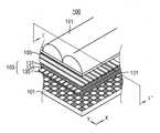
도 1은 본 발명의 실시예 1에 따른 표시장치(100)의 부분 분해 사시도이다. 도 2는 3D 모드시 도 1에 도시된 표시장치(100)를 I-I' 선을 따라 절단한 단면도이다.1 is a partially exploded perspective view of a
도 1 및 도 2를 참조하면, 표시장치(100)는 표시패널(101), 전기광학 유닛(103) 및 렌즈 유닛(105)을 포함한다.1 and 2, a
상기 표시패널(101)은 복수의 화소들을 갖고 영상을 형성한다. 상기 표시패널(101)은 영상을 형성시키는 높은 해상도 및 작은 피치 사이즈를 가지는 일반적으로 사용되는 영상 디스플레이, 예를 들어, 액정 디스플레이(liquid crystal display), 플라즈마 디스플레이, EL(electricic luminescence display) 등이 사용될 수 있다. 따라서 상기 표시패널(101)은 외부로부터 영상신호를 입력받아 이를 그대로 출력하며, 일반적인 영상구현 매체라면 사용 가능하다.The
본 실시예에서, 상기 표시패널(101)은 액정표시패널(101)을 예로 들어 설명한다. 상기 액정표시패널(101)은 서로 대향하는 어레이 기판(111) 및 대향 기판(113)과 이들 사이에 개재된 제1 액정층(114)을 포함한다. 상기 어레이 기판(111)에는 매트릭스 형태로 배열된 복수의 화소 영역들마다 화소 전극(115)들이 형성되어 있다. 상기 화소 전극(115)은 스위칭 소자에 연결되어 능동적으로 또한 개별적으로 온 및 오프가 제어될 수 있다.In the present embodiment, the
상기 대향 기판(113)에는 상기 화소 전극(115)과 대향하는 공통 전극(117)이 배치되어 있다. 상기 대향 기판(113)에는 상기 화소 영역별로 대응하여 R, G 및 B 칼라필터가 더 배치될 수 있다. A
상기 제1 액정층(114)은 상기 화소 전극(115)과 상기 공통 전극(137)의 사이에 개재된다.The first
상기 액정표시패널(101)은 외부의 구동부로부터 전달되어 상기 화소 전극(115)과 상기 공통 전극(117)에 인가되는 구동신호 및 배면에 제공되는 백라이트를 기초로 영상을 표시하며, 상기 영상은 2차원 영상이다.The liquid
상기 전기광학 유닛(103)의 모드에 따라 상기 2차원 영상은 상기 렌즈 유닛(105)을 통해 그대로 2차원 영상으로 표시되거나, 상기 렌즈 유닛(105)을 통해 3차원 영상으로 변환되어 표시된다.According to the mode of the electro-
도 3은 도 2에 도시된 가변 렌즈 구조를 도시하는 확대 단면도이다.3 is an enlarged sectional view showing the variable lens structure shown in Fig.
도 2 및 도 3을 참조하면, 상기 전기광학 유닛(103)은 선택된 모드에 따라 상기 표시패널(101)로부터 출사된 영상을 그대로 통과시키거나 3차원 영상으로 변환시킨다. 상기 전기광학 유닛(103)은 하부 기판(131), 하부 전극 라인(135)들, 상부 기판(133), 상부 전극 라인(137)들 및 제2 액정층(134)을 포함할 수 있다.2 and 3, the electro-
상기 하부 기판(131)은 상기 표시패널(101)의 표시면의 상부에 배치된다. 상기 상부 기판(133)은 상기 하부 기판(131)의 상부에 배치된다. 상기 하부 기판(131) 및 상기 상부 기판(133)은 투광성을 갖는 글라스 또는 플라스틱으로 제조 될 수 있다.The
상기 하부 전극 라인(135)들은, 도 1 및 도 3에 도시된 것과 같이, 상기 하부 기판(131)의 상면에 제1 방향(x)으로 연장되게 형성되어 있다. 상기 하부 전극 라인(135)과 상기 하부 기판(131)의 사이에는 제1 절연층(도시되지 않음)이 형성될 수 있으며, 상기 하부 전극 라인(135)들은 제2 절연층에 의해 커버되어 서로 전기적으로 절연되어 있다.1 and 3, the
각 상기 하부 전극 라인(135)은 상기 표시패널(101)의 각 상기 화소 영역에 대응하도록 배치된다. 따라서 상기 하부 전극 라인(135)의 선폭은 상기 화소 영역 또는 상기 화소 전극(135)과 거의 비슷할 수 있다. 상기 하부 전극 라인(135)의 단부는 외부의 상기 구동부와 전기적으로 연결되어 모드 선택신호를 인가 받을 수 있다.Each of the
상기 상부 전극 라인(137)들은 상기 상부 기판(133)의 하면에 상기 제1 방향(x)과 직교하는 제2 방향(y)으로 연장되어 있다. 상기 하부 전극 라인(135) 및 상기 상부 전극 라인(137)은 상기 화소 전극(135)과 동일하게 광투과성을 갖는 투명한 전도성 물질, 예를 들어, 인튬틴옥사이드(ITO) 또는 인듐주석옥사이드(IZO)를 사용하여 형성시킬 수 있다.The
상기 상부 전극 라인(137)과 상기 하부 전극 라인(135)이 서로 중첩되는 영역은 상기 표시패널(101)의 상기 화소 영역에 각기 대응될 수 있다. 즉, 상기 상부 전극 라인(137) 및 상기 하부 전극 라인(135)의 선폭이 상기 화소 영역의 사이즈에 대응하게 형성되므로, 상기 하부 전극에 의해 전원이 인가되는 상기 제2 액정 층(134)을 상기 화소 단위로 제어할 수 있게 된다.A region where the
상기 제2 액정층(134)은 상기 하부 전극 라인(135)과 상기 상부 전극 라인(137)의 사이에 개재된다. 상기 제2 액정층(134)은 외부 전원에 의해 굴절률이 변화되는 전기광학 물질을 사용한다. 상기 제2 액정층(134)은, 예를 들어, 상기 전기광학 물질로서 액정(liquid crystal) 또는 액정폴리에스테르(liquid crystal polyester)를 사용할 수 있다.The second
상기 하부 전극 라인(135) 및 상기 상부 전극 라인(137) 상에는 배향막이 더 형성될 수 있다. 상기 배향막은 공지 기술에 의해 배향처리될 수 있고, 배향처리된 상기 배향막에 의해 상기 외부 전원이 인가되지 않은 상태에서 상기 액정, 예를 들어, 네마틱 액정은 상기 하부 기판(131) 및 상기 상부 기판(133)과 수평을 이루도록 배향될 수 있다.An alignment layer may be further formed on the
상기 하부 전극 라인(135) 및 상기 상부 전극 라인(137)에 상기 외부 전원이 인가되면, 상기 네마틱 액정의 경우 상기 외부 전원의 크기에 따라 방위가 변경되어 굴절률이 변경된다. 상기 네마틱 액정의 굴절률은 1.52 내지 1.75의 범위에서 변경될 수 있다. 이러한 굴절률의 변화에 따라 통과되는 광량의 변화가 생기게 된다.When the external power is applied to the
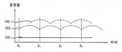
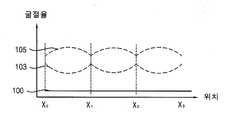
도 4는 도 2에 도시된 표시장치(100)의 위치에 따른 굴절률을 나타내는 그래프이다.FIG. 4 is a graph showing the refractive index according to the position of the
도 2 내지 도 4를 참조하면, 상기 제1 방향(x)과 직교하는 제2 방향(y)으로 상기 하부 전극 라인(135) 및 상기 상부 전극 라인(137)에 인가되는 상기 외부 전 원의 레벨을 순차적으로 달리하고 주기적으로 변경시키면, 상기 액정의 방위도 주기적으로 변경되게 상기 액정이 배열된다. 주기적으로 형성된 상기 액정의 어레이를 가변 렌즈 구조로 정의한다. 상기 가변 렌즈 구조는 셀포크 렌즈(self focusing lens)로도 불리며, 일종의 렌즈 역할을 할 수 있다. 상기 외부 전원의 인가 방식에 따라 도 4에 도시된 상기 가변 렌즈 구조의 피치(P)와 굴절률 분포가 변경될 수 있다.2 to 4, the level of the external power source applied to the
도 4에서 가로축은 상기 표시장치(100)의 일측 에지로부터 상기 제1 방향(x)과 직교하는 제2 방향(y)으로의 이격 거리를 나타낸다. 도 4에 도시된 X1, X2 및 X3은, 도 2에 도시된 것과 같이, 볼록 렌즈 형상으로 형성된 상기 가변 렌즈 구조의 마디에 대응하는 위치를 표시한다. 상기 가변 렌즈 구조의 굴절률은 볼록 렌즈와 같이 중심에 근접할수록 증가함을 알 수 있다.4, the abscissa represents the distance from one edge of the
상기 가변 렌즈 구조는 상기 제1 방향(x)으로 연장되어, 전체적으로 상기 가변 렌즈 구조는 렌티큘러(lenticular) 구조로 형성된다.The variable lens structure extends in the first direction (x), and the variable lens structure as a whole is formed in a lenticular structure.
상기 렌즈 유닛(105)은 상기 전기광학 유닛(103)의 상부에 배치된다. 상기 렌즈 유닛(105)은 광 투과율, 광 확산율, 내열성, 내화학성 및 기계적 강도 등이 우수한 고분자 수지(polymer resin)를 사용하여 제조될 수 있다. 상기 고분자 수지의 예로는 폴리메틸메타크릴레이트(Polymethylmethacrylate), 폴리아미드(polyamide), 폴리이미드(polyimide), 폴리프로필렌(polypropylene) 및 폴리우레탄(polyurethane) 등을 들 수 있다.The
상기 렌즈 유닛(105)은 시트 형상 베이스 필름과 상기 베이스 필름의 상면에 형성된 렌즈부(151)들을 포함한다. 상기 렌즈부(151)는, 도 1에 도시된 바와 같이, 상기 제1 방향(x)으로 연장된 렌티큘러 렌즈일 수 있다.The
도 2 및 도 3을 참조하면, 상기 가변 렌즈 구조는 피치(P)가 상기 렌즈부(151)의 피치(P)와 실질적으로 동일하게 형성될 수 있다. 상기 가변 렌즈 구조는, 예를 들어, 9개의 하부 전극 라인(135)들을 포함하는 피치(P)를 갖는다. 따라서 하나의 상기 렌즈부(151)의 폭 내에는 9개의 상기 하부 전극 라인(135) 및 따라서 9개의 화소들이 상기 제2 방향(y)으로 배열되어 있다.Referring to FIGS. 2 and 3, the variable lens structure may be formed such that the pitch P is substantially equal to the pitch P of the
이하, 상기 표시패널(101)의 3차원 영상이 구현되는 원리를 설명한다.Hereinafter, the principle of implementing the three-dimensional image of the
도 3에는 설명의 편의상 하나의 상기 렌즈부(151)의 피치(P) 내에 9개의 화소가 대응되게 표시되어 있다. 상기 9개의 화소들에는 어떤 물체를 3차원적으로 촬상한 영상이 표시된다. 즉, 상기 9개의 화소들에는 상기 물체를 다양한 각도에서 촬상한 영상신호가 표시된다.In Fig. 3, nine pixels are correspondingly displayed within the pitch P of one
예를 들어, 3B 화소로부터 출사된 3B 영상 신호(L1)는 상기 가변 렌즈 구조의 3B 하부 전극으로 입사되며, 상기 가변 렌즈 구조에 의해 상기 렌즈부(151)의 초점을 지나는 중심선을 향하여 굴절된다. 상기 가변 렌즈 구조에 의해 굴절된 상기 3B 영상 신호는 상기 렌즈부(151)에 의해 굴절되어 관찰자의 좌측 눈(E1)에 입사된다.For example, the 3B image signal L1 emitted from the 3B pixel is incident on the 3B lower electrode of the variable lens structure, and is refracted toward the center line passing through the focal point of the
이와 동시에, 3H 화소로부터 출사된 3H 영상 신호(L2)는 상기 가변 렌즈 구조의 3H 하부 전극으로 입사되며, 상기 가변 렌즈 구조에 의해 상기 렌즈부(151)의 초점을 지나는 중심선을 향하여 굴절된다. 상기 가변 렌즈 구조에 의해 굴절된 상 기 3H 영상 신호는 상기 렌즈부(151)에 의해 굴절되어 관찰자의 우측 눈(E2)에 입사된다.Simultaneously, the 3H image signal L2 emitted from the 3H pixel is incident on the 3H lower electrode of the variable lens structure, and is refracted toward the center line passing through the focal point of the
따라서, 관찰자의 좌측 눈(E1) 및 우측 눈(E2)에 서로 다른 영상 신호, 특히 상기 물체를 복수의 방향에서 촬상한 영상신호가 관찰자에게 입력된다. 따라서 관찰자의 뇌는 입체감을 느끼게 되어 상기 표시장치(100)는 3차원 영상을 표시한 것이 된다.Therefore, different image signals are input to the left eye E1 and the right eye E2 of the observer, and in particular, image signals obtained by imaging the object in a plurality of directions are input to the observer. Accordingly, the observer's brain senses a three-dimensional sensation, and the
도 4를 참조하면, 상기 영상 신호는 상기 가변 렌즈 구조의 굴절률과 상기 렌즈부(151)의 굴절률의 영향이 종합된 표시장치(100)의 굴절률에 의해 굴절되어 3차원 영상이 표시된다. 상기 가변 렌즈 구조의 굴절률을 조절하여 상기 표시장치(100)의 굴절률을 조절할 수 있고, 따라서 상기 표시장치(100)의 초점 거리를 조절할 수 있다.Referring to FIG. 4, the image signal is refracted by the refractive index of the
이하, 상기 표시패널(101)의 2차원 영상이 구현되는 원리를 설명한다.Hereinafter, the principle of implementing the two-dimensional image of the
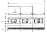
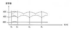
도 5는 일 예의 2D 모드시 도 1에 도시된 표시장치(100)를 I-I' 선을 따라 절단한 단면도이다. 도 6은 도 5에 도시된 표시장치(100)의 위치에 따른 굴절률을 나타내는 그래프이다.5 is a cross-sectional view of the
도 5 및 도 6을 참조하면, 2D 모드(2차원 모드)에서 상기 가변 렌즈 구조는 전술된 3D 모드(3차원 모드)에서의 피치(P)보다 1/2 피치(P)만큼 이동되어 동일한 크기의 피치(P)로 형성될 수 있다. 따라서 상기 가변 렌즈 구조의 초점은 상기 렌즈부(151)들의 초점을 지나는 중심선들의 사이에 배치된다. 즉 상기 렌즈 구조의 초점은 상기 렌즈부(151)들이 서로 연결되는 마디에 대응하게 배치된다.5 and 6, in the 2D mode (two-dimensional mode), the variable lens structure is shifted by a half pitch (P) from the pitch P in the 3D mode (three-dimensional mode) (P). Accordingly, the focal point of the variable lens structure is disposed between the center lines passing through the focal points of the
따라서, 도 6에 도시된 바와 같이, 상기 렌즈부(151)의 굴절률과 상기 가변 렌즈 구조의 굴절율을 합산한 표시패널(101)의 굴절률 값은 위치에 따라 거의 비슷하게 된다. 따라서 상기 표시패널(101)로부터 출사된 영상 신호들(L1, L2)은 초점을 형성하지 않고 상기 표시패널(101)에 수직한 방향으로 출사된다. 따라서 관찰자의 좌측 눈(E1) 및 우측 눈(E2)에는 서로 다른 영상이 각기 입력되지 않고 하나의 영상 신호가 입력된다. 따라서 관찰자는 평면 영상, 즉 2차원 영상을 느끼게 되어 상기 표시장치(100)는 2차원 영상을 표시한다.6, the refractive index of the
도 7은 다른 예의 2D 모드시 도 1에 도시된 표시장치(100)를 I-I' 선을 따라 절단한 단면도이다. 도 8은 도 7에 도시된 표시장치(100)의 위치에 따른 굴절률을 나타내는 그래프이다.7 is a cross-sectional view of the
도 7 및 도 8을 참조하면, 상기 가변 렌즈 구조는, 도 2 내지 도 6에서 설명된 것과 다르게, 피치(P)가 상기 렌즈부(151)와 일치하지만 오목 렌즈 구조로 형성될 수 있다. 따라서 굴절률 분포는, 도 8에 도시된 것과 같이, 상기 렌즈부(151)와 상기 가변 랜즈부의 굴절률 상쇄되는 형태로 분포된다. 따라서 상기 표시패널(101)의 굴절률은 위치에 따라 균일하여 상기 표시패널(101)은 2차원 영상을 표시한다.7 and 8, the variable lens structure may be formed in a concave lens structure although the pitch P is the same as the
본 실시예에 의하면, 렌즈부(151)의 굴절률과 상기 가변 렌즈부(151)의 굴절율이 종합된 표시패널(101)의 굴절률에 의하여 3차원 또는 2차원 영상을 구현한다. 따라서 상기 렌즈 유닛(105)의 상기 렌즈부(151) 또는 상기 전기광학 유닛(103)의 셀겝 각각의 두께를 100 마이크로미터 이하로 형성하여도 상기 표시장치(100)가 3차원 영상을 표시하기 위해 필요한 초점 거리를 확보할 수 있다. 따라서 상기 표시 패널(101)을 대형화시킬 수 있다.According to the present embodiment, a three-dimensional or two-dimensional image is realized by the refractive index of the
또한, 전기광학 유닛(103)을 전기광학적으로 구동시키는 것만으로 2차원 모드 및 3차원 모드의 전환이 이루어져서 모드 전환이 매우 용이한 표시장치(100)를 구현할 수 있다.In addition, the
실시예 2Example 2
도 9는 실시예 2에 따른 표시장치(400)의 3D 모드시의 단면도이다. 도 10은 도 9에 도시된 표시장치(400)의 위치에 따른 굴절률을 나타내는 그래프이다.9 is a sectional view of the
도 9 및 도 10을 참조하면, 표시장치(400)는 렌즈 유닛(405) 대신 전기광학 유닛(403)을 포함하는 것을 제외하고는 도 1 내지 도 6에서 설명된 표시장치(100)와 실질적으로 동일하다.9 and 10, the
본 실시예에서, 표시장치(400)는 표시패널(401), 제1 전기광학 유닛(403) 및 제2 전기광학 유닛(405)을 포함한다. 상기 제1 전기광학 유닛(403) 및 상기 제2 전기광학 유닛(405)은 실질적으로 서로 동일할 수 있다. In this embodiment, the
상기 제1 전기광학 유닛(403)은 제1 가변 렌즈 구조를 형성하고, 상기 제2 전기광학 유닛(405)은 제2 가변 렌즈 구조를 형성한다. 상기 제1 가변 렌즈 구조 및 상기 제2 가변 렌즈 구조의 피치(P) 및 중심선은 모두 실질적으로 일치하도록 하부 전극 라인(435) 및 상부 전극 라인(437)에 전원을 인가할 수 있다.The first electro-
따라서, 도 10에 도시된 것과 같이, 볼록 렌즈 형상의 표시패널(401) 굴절률이 형성되어 3차원 영상이 표시된다.Therefore, as shown in Fig. 10, the refractive index of the convex lens-shaped
도 11은 일 예의 2D 모드시 도 9에 도시된 표시장치(400)의 단면도이다. 도 12는 도 11에 도시된 표시장치(400)의 위치에 따른 굴절률을 나타내는 그래프이다.FIG. 11 is a sectional view of the
도 11 및 도 12를 참조하면, 상기 제1 가변 렌즈 구조 및 상기 제2 가변 렌즈 구조는 그 피치(P)가 서로 실질적으로 동일하고, 중심선이 1/2 피치(P)만큼 어긋나게 배열되도록 형성될 수 있다.11 and 12, the first variable lens structure and the second variable lens structure are formed such that the pitches P thereof are substantially equal to each other and the center line is arranged to be shifted by a half pitch (P) .
따라서, 도 12에 도시된 바와 같이, 상기 표시패널(401)의 굴절률은 위치에 따라 균일하게 형성되어 2차원 영상이 구현될 수 있다.Therefore, as shown in FIG. 12, the refractive index of the
도 13은 다른 예의 2D 모드시 도 9에 도시된 표시장치(400)의 단면도이다. 도 14는 도 13에 도시된 표시장치(400)의 위치에 따른 굴절률을 나타내는 그래프이다.Fig. 13 is a sectional view of the
도 13 및 도 14를 참조하면, 상기 제1 가변 렌즈 구조 및 상기 제2 가변 렌즈 구조는 그 피치(P) 및 중심선이 서로 실질적으로 동일하지만, 하나는 볼록 렌즈 구조로 다른 하나는 오목 렌즈 구조로 형성될 수 있다. 예를 들어, 도 13에서 상기 제1 가변 렌즈 구조는 볼록 렌즈 구조로 형성되어 있고, 상기 제2 가변 렌즈 구조는 오목 렌즈 구조로 형성되어 있다. 즉, 상기 제1 가변 렌즈 구조의 굴절률과 상기 제2 가변 렌즈 구조의 굴절률은 서로 상쇄되는 분포를 갖는다. 그 결과, 상기 표시패널(401)의 굴절률은 위치에 따라 균일하게 형성되어 2차원 영상이 구현될 수 있다.13 and 14, the first variable lens structure and the second variable lens structure have substantially the same pitch P and center line, but one has a convex lens structure and the other has a concave lens structure . For example, in FIG. 13, the first variable lens structure is formed in a convex lens structure, and the second variable lens structure is formed in a concave lens structure. That is, the refractive index of the first variable lens structure and the refractive index of the second variable lens structure are offset from each other. As a result, the refractive index of the
본 실시예에 의하면, 2개의 전기광학 유닛들을 사용하여 초점 거리를 보다 자유롭게 조절할 수 있고, 모드 전환에서 다양한 선택사항을 가질 수 있다.According to this embodiment, the two electro-optical units can be used to adjust the focal distance more freely, and various choices can be made in the mode switching.
본 발명의 실시예에 따른 표시장치에 의하면, 2차원 및 3차원 겸용 표시장치를 대형화하기에 매우 유리하며 2차원 및 3차원 사이에 모드 전환이 매우 용이하게 달성된다. 따라서 본 발명은 2차원 및 3차원 영상 표시를 자유롭게 구현하는 영상표시 분야에 적용될 수 있다.According to the display device according to the embodiment of the present invention, it is very advantageous to increase the size of the two-dimensional and three-dimensional combined display device, and mode switching between two-dimensional and three-dimensional is very easily achieved. Therefore, the present invention can be applied to an image display field which freely implements two-dimensional and three-dimensional image display.
앞서 설명한 본 발명의 상세한 설명에서는 본 발명의 바람직한 실시예들을 참조하여 설명하였지만, 해당 기술분야의 숙련된 당업자 또는 해당 기술분야에 통상의 지식을 갖는 자라면 후술될 특허청구범위에 기재된 본 발명의 사상 및 기술 영역으로부터 벗어나지 않는 범위 내에서 본 발명을 다양하게 수정 및 변경시킬 수 있음을 이해할 수 있을 것이다.While the present invention has been described in connection with what is presently considered to be practical and exemplary embodiments, it is to be understood that the invention is not limited to the disclosed embodiments, but, on the contrary, It will be understood by those skilled in the art that various changes in form and details may be made therein without departing from the spirit and scope of the invention as defined by the appended claims.
도 1은 본 발명의 실시예 1에 따른 표시장치의 부분 분해 사시도이다.1 is a partially exploded perspective view of a display device according to a first embodiment of the present invention.
도 2는 3D 모드시 도 1에 도시된 표시장치를 I-I 선을 따라 절단한 단면도이다.FIG. 2 is a cross-sectional view of the display device shown in FIG. 1 taken along the line I-I in the 3D mode.
도 3은 도 2에 도시된 단일 가변 렌즈 구조를 도시하는 확대 단면도이다.3 is an enlarged sectional view showing the single variable lens structure shown in Fig.
도 4는 도 2에 도시된 표시장치의 위치에 따른 굴절률을 나타내는 그래프이다.4 is a graph showing the refractive index according to the position of the display device shown in FIG.
도 5는 일 예의 2D 모드시 도 1에 도시된 표시장치를 I-I 선을 따라 절단한 단면도이다.FIG. 5 is a cross-sectional view of the display device shown in FIG. 1 taken along the line I-I in the 2D mode of one example.
도 6은 도 5에 도시된 표시장치의 위치에 따른 굴절률을 나타내는 그래프이다.6 is a graph showing the refractive index according to the position of the display device shown in FIG.
도 7은 다른 예의 2D 모드시 도 1에 도시된 표시장치를 I-I 선을 따라 절단한 단면도이다.FIG. 7 is a cross-sectional view of the display device shown in FIG. 1 taken along the line I-I in the 2D mode of another example.
도 8은 도 7에 도시된 표시장치의 위치에 따른 굴절률을 나타내는 그래프이다.8 is a graph showing the refractive index according to the position of the display device shown in FIG.
도 9는 실시예 2에 따른 표시장치의 3D 모드시의 단면도이다.9 is a sectional view of the display device according to the second embodiment in a 3D mode.
도 10은 도 9에 도시된 표시장치의 위치에 따른 굴절률을 나타내는 그래프이다.10 is a graph showing the refractive index according to the position of the display device shown in FIG.
도 11은 일 예의 2D 모드시 도 9에 도시된 표시장치의 단면도이다.Fig. 11 is a cross-sectional view of the display device shown in Fig. 9 in 2D mode in one example.
도 12는 도 11에 도시된 표시장치의 위치에 따른 굴절률을 나타내는 그래프 이다.12 is a graph showing the refractive index according to the position of the display device shown in FIG.
도 13은 다른 예의 2D 모드시 도 9에 도시된 표시장치의 단면도이다.Fig. 13 is a cross-sectional view of the display device shown in Fig. 9 in the 2D mode of another example.
도 14는 도 13에 도시된 표시장치의 위치에 따른 굴절률을 나타내는 그래프이다.14 is a graph showing the refractive index according to the position of the display device shown in Fig.
<도면의 주요 부분에 대한 부호의 설명> Description of the Related Art
100 : 표시장치101 : 표시패널100: display device 101: display panel
103 : 전기광학 유닛105 : 렌즈 유닛103: electro-optical unit 105: lens unit
131 : 하부 기판133 : 상부 기판131: lower substrate 133: upper substrate
135 : 하부 전극 라인137 : 상부 전극 라인135: lower electrode line 137: upper electrode line
134 : 액정층151 : 렌즈부134: liquid crystal layer 151: lens part
Claims (18)
Translated fromKoreanPriority Applications (2)
| Application Number | Priority Date | Filing Date | Title |
|---|---|---|---|
| KR1020080074735AKR101472052B1 (en) | 2008-07-30 | 2008-07-30 | Display device |
| US12/511,727US8300206B2 (en) | 2008-07-30 | 2009-07-29 | Electro-optic unit having electro-optic material layer with variable refractive index, driving method of the electro-optic unit, and display apparatus having the same |
Applications Claiming Priority (1)
| Application Number | Priority Date | Filing Date | Title |
|---|---|---|---|
| KR1020080074735AKR101472052B1 (en) | 2008-07-30 | 2008-07-30 | Display device |
Publications (2)
| Publication Number | Publication Date |
|---|---|
| KR20100013179A KR20100013179A (en) | 2010-02-09 |
| KR101472052B1true KR101472052B1 (en) | 2014-12-12 |
Family
ID=41607976
Family Applications (1)
| Application Number | Title | Priority Date | Filing Date |
|---|---|---|---|
| KR1020080074735AExpired - Fee RelatedKR101472052B1 (en) | 2008-07-30 | 2008-07-30 | Display device |
Country Status (2)
| Country | Link |
|---|---|
| US (1) | US8300206B2 (en) |
| KR (1) | KR101472052B1 (en) |
Families Citing this family (78)
| Publication number | Priority date | Publication date | Assignee | Title |
|---|---|---|---|---|
| DE112010003840B4 (en)* | 2009-09-29 | 2022-10-20 | Seereal Technologies S.A. | Light modulator for a display, display and a method for operating a light modulator |
| US9507198B2 (en) | 2009-11-19 | 2016-11-29 | Apple Inc. | Systems and methods for electronically controlling the viewing angle of a display |
| KR101274717B1 (en)* | 2009-12-24 | 2013-06-12 | 엘지디스플레이 주식회사 | Liquid Crystal Lens Electrically driven and Stereoscopy Display Device Using the Same |
| KR101772153B1 (en)* | 2010-03-17 | 2017-08-29 | 삼성디스플레이 주식회사 | Display device using diffractive lens |
| RU2582888C2 (en)* | 2010-05-21 | 2016-04-27 | Конинклейке Филипс Электроникс Н.В. | Convertible 2d/3d display device |
| TWI435116B (en)* | 2010-09-27 | 2014-04-21 | Au Optronics Corp | Stereo display and image display method thereof |
| KR101698571B1 (en)* | 2010-10-29 | 2017-02-02 | 삼성디스플레이 주식회사 | Display device using diffractive device |
| CN102062985B (en)* | 2010-11-16 | 2012-02-22 | 深圳超多维光电子有限公司 | Liquid crystal lens, control method thereof, and 3D display device |
| JP5286349B2 (en) | 2010-12-27 | 2013-09-11 | 株式会社東芝 | Gradient index liquid crystal optical element and image display device |
| KR101707587B1 (en)* | 2010-12-28 | 2017-02-17 | 삼성디스플레이 주식회사 | Display device using diffractive device |
| CN102109706A (en)* | 2011-02-11 | 2011-06-29 | 深圳超多维光电子有限公司 | Stereoscopic display and grating thereof |
| GB2488978A (en) | 2011-03-07 | 2012-09-19 | Sharp Kk | Switching lenses for multi-view displays |
| GB2488979A (en)* | 2011-03-07 | 2012-09-19 | Sharp Kk | Switchable Optics with GRIN lenses formed in liquid crystal layer |
| CN102480007B (en)* | 2011-04-12 | 2013-06-12 | 深圳光启高等理工研究院 | Metamaterial capable of converging electromagnetic wave |
| RU2013151162A (en) | 2011-04-19 | 2015-05-27 | Конинклейке Филипс Н.В. | LIGHT OUTPUT PANEL AND DEVICE HAVING IT |
| KR101921172B1 (en)* | 2011-05-18 | 2018-11-23 | 삼성디스플레이 주식회사 | Display device and method of masufacturing the same |
| JP5588399B2 (en)* | 2011-06-28 | 2014-09-10 | 株式会社ジャパンディスプレイ | Display device and variable lens array |
| JPWO2013038557A1 (en)* | 2011-09-16 | 2015-03-23 | 株式会社東芝 | Gradient index liquid crystal optical element and image display device |
| KR101852121B1 (en) | 2011-11-18 | 2018-06-12 | 삼성디스플레이 주식회사 | Display device |
| WO2013105240A1 (en)* | 2012-01-11 | 2013-07-18 | 株式会社 東芝 | Liquid crystal optical element and three-dimensional image display device |
| WO2013119066A1 (en) | 2012-02-07 | 2013-08-15 | 주식회사 엘지화학 | Liquid crystal lens |
| JP5583158B2 (en)* | 2012-02-29 | 2014-09-03 | 株式会社東芝 | Liquid crystal optical element, driving device and image display device |
| KR101859483B1 (en)* | 2012-03-06 | 2018-06-27 | 엘지디스플레이 주식회사 | Stereoscopic display device and method for manufacturing the same |
| KR20130107953A (en) | 2012-03-23 | 2013-10-02 | 삼성디스플레이 주식회사 | Display device |
| WO2014018269A1 (en)* | 2012-07-23 | 2014-01-30 | Reald Inc. | Observer tracking autostereoscopic display |
| JP5921376B2 (en)* | 2012-08-01 | 2016-05-24 | 株式会社ジャパンディスプレイ | 3D display device |
| TWI471608B (en)* | 2012-09-03 | 2015-02-01 | Wintek Corp | Naked eye type and glasses type switchable stereoscopic display device |
| AU2013322130B2 (en) | 2012-09-30 | 2017-03-09 | Optica Amuka (A.A.) Ltd. | Lenses with electrically-tunable power and alignment |
| US11126040B2 (en) | 2012-09-30 | 2021-09-21 | Optica Amuka (A.A.) Ltd. | Electrically-tunable lenses and lens systems |
| KR20140053741A (en)* | 2012-10-26 | 2014-05-08 | 삼성디스플레이 주식회사 | A liquid crystal lens, a liquid crystal module having the liquid crystal lens and a method for driving the liquid crystal module |
| JP2014089294A (en)* | 2012-10-30 | 2014-05-15 | Toshiba Corp | Liquid crystal lens device and method for driving the same |
| CN102928904B (en)* | 2012-11-16 | 2015-09-23 | 京东方科技集团股份有限公司 | Lenticulation and display device |
| TWI471667B (en)* | 2012-11-30 | 2015-02-01 | Au Optronics Corp | Liquid crystal lens and stereo display using the same |
| CN103852936B (en)* | 2012-12-04 | 2017-06-16 | 乐金显示有限公司 | Stereoscopic display device |
| CN103048842A (en)* | 2012-12-10 | 2013-04-17 | 京东方科技集团股份有限公司 | Liquid crystal lens and three-dimensional display device |
| KR102000146B1 (en)* | 2012-12-27 | 2019-09-27 | 엘지디스플레이 주식회사 | Light Control Cell And Image Display Device Including The Same |
| US9118143B2 (en) | 2012-12-28 | 2015-08-25 | Intel Corporation | Mechanism for facilitating and employing a magnetic grid array |
| US9842562B2 (en)* | 2013-01-13 | 2017-12-12 | Qualcomm Incorporated | Dynamic zone plate augmented vision eyeglasses |
| US9857593B2 (en) | 2013-01-13 | 2018-01-02 | Qualcomm Incorporated | Optics display system with dynamic zone plate capability |
| KR102082996B1 (en) | 2013-02-13 | 2020-03-02 | 삼성디스플레이 주식회사 | Three dimensional image display and liquid crystal lens therefor |
| TWI495926B (en)* | 2013-07-08 | 2015-08-11 | Au Optronics Corp | Lc lens device and method for driving lc lens |
| KR102232621B1 (en)* | 2013-07-30 | 2021-03-29 | 삼성디스플레이 주식회사 | Display apparatus providing light therapy |
| US9151971B2 (en)* | 2013-09-17 | 2015-10-06 | Boe Technology Group Co., Ltd | Liquid crystal lens and stereoscopic display device |
| KR102061234B1 (en) | 2013-10-28 | 2020-01-02 | 삼성디스플레이 주식회사 | Display device and liquid crystal lends panel for the same |
| CN103744248A (en)* | 2013-11-28 | 2014-04-23 | 深圳市华星光电技术有限公司 | Display device and liquid crystal box lens panel |
| CN103728807B (en)* | 2013-11-28 | 2016-10-05 | 深圳市华星光电技术有限公司 | Display device and liquid crystal cell lens panel |
| CN103676171B (en)* | 2013-12-19 | 2016-01-27 | 京东方科技集团股份有限公司 | 3d display device |
| KR102271203B1 (en)* | 2013-12-23 | 2021-06-30 | 삼성디스플레이 주식회사 | Display device |
| JP6515115B2 (en)* | 2014-03-13 | 2019-05-15 | オプティカ アムカ(エー.エー.)リミテッド | Electrically adjustable lens and lens system |
| US9494726B2 (en)* | 2014-05-27 | 2016-11-15 | Microsoft Technology Licensing, Llc | Switchable backlight unit |
| EP3152602B1 (en)* | 2014-06-05 | 2019-03-20 | Optica Amuka (A.A.) Ltd. | Dynamic lenses and method of manufacturing thereof |
| TWI533665B (en)* | 2014-09-02 | 2016-05-11 | 深圳超多維光電子有限公司 | Stereoscopic display device |
| KR102207192B1 (en)* | 2014-09-30 | 2021-01-25 | 엘지디스플레이 주식회사 | Polarizing Control Film and Stereoscopic Display Device Using the Same |
| KR102371780B1 (en) | 2015-01-08 | 2022-03-08 | 삼성디스플레이 주식회사 | A liquid crystal panel and a display apparatus comprising the same |
| KR20160087461A (en) | 2015-01-13 | 2016-07-22 | 삼성디스플레이 주식회사 | Optical modulation device and driving method thereof |
| JP6508012B2 (en)* | 2015-02-10 | 2019-05-08 | 株式会社デンソー | Tool holder and method of manufacturing the same |
| CN105607380A (en)* | 2016-03-29 | 2016-05-25 | 京东方科技集团股份有限公司 | Liquid crystal lens, display device and driving method thereof |
| ES2904889T3 (en)* | 2016-04-17 | 2022-04-06 | Optica Amuka A A Ltd | Spectacle lens comprising an improved electrically actuated liquid crystal lens |
| WO2017216716A1 (en) | 2016-06-16 | 2017-12-21 | Optica Amuka (A.A.) Ltd. | Tunable lenses for spectacles |
| CN107870382B (en) | 2016-09-26 | 2019-11-05 | 京东方科技集团股份有限公司 | A kind of slit grating and three-dimensional display apparatus |
| CN106526950A (en)* | 2016-11-25 | 2017-03-22 | 张家港康得新光电材料有限公司 | Three-dimensional display device |
| CN108107572B (en) | 2016-11-25 | 2020-07-14 | 中强光电股份有限公司 | near-eye display device |
| CN106681079B (en)* | 2017-01-22 | 2018-11-02 | 惠科股份有限公司 | Liquid crystal lens and display device |
| CN106802502B (en)* | 2017-04-10 | 2018-10-30 | 京东方科技集团股份有限公司 | Liquid crystal diffraction zone plate, liquid crystal display panel, display methods, display device |
| US11747619B2 (en) | 2017-07-10 | 2023-09-05 | Optica Amuka (A.A.) Ltd. | Virtual reality and augmented reality systems with dynamic vision correction |
| US11953764B2 (en) | 2017-07-10 | 2024-04-09 | Optica Amuka (A.A.) Ltd. | Tunable lenses with enhanced performance features |
| CN109471256A (en) | 2017-09-07 | 2019-03-15 | 中强光电股份有限公司 | Optical components and display devices |
| WO2019077442A1 (en) | 2017-10-16 | 2019-04-25 | Optica Amuka (A.A.) Ltd. | Spectacles with electrically-tunable lenses controllable by an external system |
| US11086143B1 (en) | 2018-06-11 | 2021-08-10 | Apple Inc. | Tunable and foveated lens systems |
| JP7015928B2 (en) | 2018-08-28 | 2022-02-03 | 株式会社ソニー・インタラクティブエンタテインメント | Lens unit and image observation device |
| WO2020045518A1 (en)* | 2018-08-28 | 2020-03-05 | 株式会社ソニー・インタラクティブエンタテインメント | Lens system and image observation device |
| US11703698B1 (en) | 2018-08-30 | 2023-07-18 | Apple Inc. | Adjustable lens systems |
| US10810971B2 (en)* | 2018-12-31 | 2020-10-20 | Samsung Electronics Co., Ltd. | Multi-view display system and method therefor |
| EP3977199A4 (en) | 2019-06-02 | 2023-06-14 | Optica Amuka (A.A.) Ltd. | Electrically-tunable vision aid for treatment of myopia |
| US11460745B2 (en)* | 2020-06-10 | 2022-10-04 | Sharp Kabushiki Kaisha | Display with two thin film transistor substrates |
| GB2613267B (en)* | 2020-08-31 | 2025-02-12 | Alphamicron Incorporated | Graduated electro-optic device and method |
| JP2022070474A (en)* | 2020-10-27 | 2022-05-13 | 株式会社ジャパンディスプレイ | LCD device |
| KR102852912B1 (en)* | 2021-08-23 | 2025-09-02 | 가부시키가이샤 재팬 디스프레이 | Liquid crystal light control elements and lighting devices |
Citations (4)
| Publication number | Priority date | Publication date | Assignee | Title |
|---|---|---|---|---|
| JPH1048597A (en)* | 1996-07-31 | 1998-02-20 | Nippon Telegr & Teleph Corp <Ntt> | Optical device |
| JPH1074052A (en)* | 1996-08-30 | 1998-03-17 | Nippon Telegr & Teleph Corp <Ntt> | 3D display device |
| JP2000102038A (en)* | 1998-09-18 | 2000-04-07 | Sanyo Electric Co Ltd | Two-dimensional video image and three-dimensional video image compatible type video display device |
| KR20030022583A (en)* | 2001-09-11 | 2003-03-17 | 삼성전자주식회사 | 2d/3d convertible display |
Family Cites Families (13)
| Publication number | Priority date | Publication date | Assignee | Title |
|---|---|---|---|---|
| US5122888A (en)* | 1987-07-10 | 1992-06-16 | Canon Kabushiki Kaisha | Focusing plate having phase grating formed by using liquid crystal |
| US6469683B1 (en)* | 1996-01-17 | 2002-10-22 | Nippon Telegraph And Telephone Corporation | Liquid crystal optical device |
| US6626532B1 (en)* | 1997-06-10 | 2003-09-30 | Olympus Optical Co., Ltd. | Vari-focal spectacles |
| US7369327B1 (en)* | 1998-06-09 | 2008-05-06 | Olympus Corporation | Variable optical-property element and optical apparatus including the same |
| JP2000261833A (en) | 1999-03-11 | 2000-09-22 | Oki Data Corp | 3D display device |
| US6864951B1 (en)* | 2002-05-08 | 2005-03-08 | University Of Central Florida | Tunable electronic lens and prisms using inhomogeneous nano scale liquid crystal droplets |
| JP3969252B2 (en) | 2002-08-27 | 2007-09-05 | 日本電気株式会社 | Stereoscopic image plane image switching display device and portable terminal device |
| JP4227828B2 (en)* | 2002-10-07 | 2009-02-18 | 佐藤 進 | Flat lens |
| KR20060126668A (en)* | 2004-02-03 | 2006-12-08 | 아사히 가라스 가부시키가이샤 | Liquid Crystal Lens Element and Optical Head Device |
| GB2411735A (en)* | 2004-03-06 | 2005-09-07 | Sharp Kk | Control of liquid crystal alignment in an optical device |
| KR101122199B1 (en)* | 2005-07-07 | 2012-03-19 | 삼성전자주식회사 | 2D-3D switchable autostereoscopic display apparatus |
| US7995166B2 (en)* | 2007-05-07 | 2011-08-09 | Nec Lcd Technologies, Ltd. | Display panel, display device, and terminal device |
| GB2455614B (en)* | 2007-12-14 | 2010-02-17 | Lg Display Co Ltd | Electrically-driven liquid crystal lens and stereoscopic display device using the same |
- 2008
- 2008-07-30KRKR1020080074735Apatent/KR101472052B1/ennot_activeExpired - Fee Related
- 2009
- 2009-07-29USUS12/511,727patent/US8300206B2/ennot_activeExpired - Fee Related
Patent Citations (4)
| Publication number | Priority date | Publication date | Assignee | Title |
|---|---|---|---|---|
| JPH1048597A (en)* | 1996-07-31 | 1998-02-20 | Nippon Telegr & Teleph Corp <Ntt> | Optical device |
| JPH1074052A (en)* | 1996-08-30 | 1998-03-17 | Nippon Telegr & Teleph Corp <Ntt> | 3D display device |
| JP2000102038A (en)* | 1998-09-18 | 2000-04-07 | Sanyo Electric Co Ltd | Two-dimensional video image and three-dimensional video image compatible type video display device |
| KR20030022583A (en)* | 2001-09-11 | 2003-03-17 | 삼성전자주식회사 | 2d/3d convertible display |
Also Published As
| Publication number | Publication date |
|---|---|
| US20100026920A1 (en) | 2010-02-04 |
| US8300206B2 (en) | 2012-10-30 |
| KR20100013179A (en) | 2010-02-09 |
Similar Documents
| Publication | Publication Date | Title |
|---|---|---|
| KR101472052B1 (en) | Display device | |
| US8786683B2 (en) | Stereoscopic display unit | |
| TWI472802B (en) | Display device | |
| KR100440956B1 (en) | 2D/3D Convertible Display | |
| KR101241770B1 (en) | Stereo-scopic image conversion panel and stereo-scopic image display apparatus having the same | |
| EP1750459B1 (en) | High-resolution autostereoscopic display | |
| US7630131B2 (en) | Image display apparatus and optical member therefor | |
| US7969517B2 (en) | Electrically-driven liquid crystal lens and stereoscopic display device using the same | |
| CN101218833B (en) | Autostereoscopic display apparatus | |
| CN102819147B (en) | Display device | |
| KR102006481B1 (en) | Multi-view display device | |
| JP5667928B2 (en) | Image display device | |
| KR100477638B1 (en) | 2D/3D convertible display | |
| US20100295930A1 (en) | Stereoscopic method and a device for implementation thereof | |
| JP2010224191A (en) | Stereoscopic image display device | |
| RU2542593C2 (en) | Auto stereoscopic display device | |
| US20130088529A1 (en) | Display unit | |
| KR20100074015A (en) | Lens array device and image display | |
| JP2011154197A (en) | 3d display | |
| KR20140017455A (en) | Stereoscopic display apparatus | |
| US10247950B2 (en) | Three-dimensional image display device | |
| KR20130067223A (en) | Liquid crystal display device, electronic apparatus, and optical device | |
| JP4929636B2 (en) | Liquid crystal display | |
| KR20100137725A (en) | Switching stereoscopic filter and switching stereoscopic image display device using the same | |
| KR101147088B1 (en) | Display Switchable Mode Liquid Crystal Display Device |
Legal Events
| Date | Code | Title | Description |
|---|---|---|---|
| PA0109 | Patent application | St.27 status event code:A-0-1-A10-A12-nap-PA0109 | |
| PG1501 | Laying open of application | St.27 status event code:A-1-1-Q10-Q12-nap-PG1501 | |
| R18-X000 | Changes to party contact information recorded | St.27 status event code:A-3-3-R10-R18-oth-X000 | |
| N231 | Notification of change of applicant | ||
| PN2301 | Change of applicant | St.27 status event code:A-3-3-R10-R13-asn-PN2301 St.27 status event code:A-3-3-R10-R11-asn-PN2301 | |
| A201 | Request for examination | ||
| PA0201 | Request for examination | St.27 status event code:A-1-2-D10-D11-exm-PA0201 | |
| E902 | Notification of reason for refusal | ||
| PE0902 | Notice of grounds for rejection | St.27 status event code:A-1-2-D10-D21-exm-PE0902 | |
| E13-X000 | Pre-grant limitation requested | St.27 status event code:A-2-3-E10-E13-lim-X000 | |
| P11-X000 | Amendment of application requested | St.27 status event code:A-2-2-P10-P11-nap-X000 | |
| P13-X000 | Application amended | St.27 status event code:A-2-2-P10-P13-nap-X000 | |
| E701 | Decision to grant or registration of patent right | ||
| PE0701 | Decision of registration | St.27 status event code:A-1-2-D10-D22-exm-PE0701 | |
| GRNT | Written decision to grant | ||
| PR0701 | Registration of establishment | St.27 status event code:A-2-4-F10-F11-exm-PR0701 | |
| PR1002 | Payment of registration fee | St.27 status event code:A-2-2-U10-U11-oth-PR1002 Fee payment year number:1 | |
| PG1601 | Publication of registration | St.27 status event code:A-4-4-Q10-Q13-nap-PG1601 | |
| R18-X000 | Changes to party contact information recorded | St.27 status event code:A-5-5-R10-R18-oth-X000 | |
| FPAY | Annual fee payment | Payment date:20171129 Year of fee payment:4 | |
| PR1001 | Payment of annual fee | St.27 status event code:A-4-4-U10-U11-oth-PR1001 Fee payment year number:4 | |
| FPAY | Annual fee payment | Payment date:20181126 Year of fee payment:5 | |
| PR1001 | Payment of annual fee | St.27 status event code:A-4-4-U10-U11-oth-PR1001 Fee payment year number:5 | |
| R18-X000 | Changes to party contact information recorded | St.27 status event code:A-5-5-R10-R18-oth-X000 | |
| PR1001 | Payment of annual fee | St.27 status event code:A-4-4-U10-U11-oth-PR1001 Fee payment year number:6 | |
| PC1903 | Unpaid annual fee | St.27 status event code:A-4-4-U10-U13-oth-PC1903 Not in force date:20201206 Payment event data comment text:Termination Category : DEFAULT_OF_REGISTRATION_FEE | |
| PC1903 | Unpaid annual fee | St.27 status event code:N-4-6-H10-H13-oth-PC1903 Ip right cessation event data comment text:Termination Category : DEFAULT_OF_REGISTRATION_FEE Not in force date:20201206 |