KR101471945B1 - Backlight assembly - Google Patents
Backlight assemblyDownload PDFInfo
- Publication number
- KR101471945B1 KR101471945B1KR1020080096634AKR20080096634AKR101471945B1KR 101471945 B1KR101471945 B1KR 101471945B1KR 1020080096634 AKR1020080096634 AKR 1020080096634AKR 20080096634 AKR20080096634 AKR 20080096634AKR 101471945 B1KR101471945 B1KR 101471945B1
- Authority
- KR
- South Korea
- Prior art keywords
- light source
- boundary
- substrate
- storage container
- coupling protrusion
- Prior art date
- Legal status (The legal status is an assumption and is not a legal conclusion. Google has not performed a legal analysis and makes no representation as to the accuracy of the status listed.)
- Expired - Fee Related
Links
Images


Classifications
- G—PHYSICS
- G02—OPTICS
- G02F—OPTICAL DEVICES OR ARRANGEMENTS FOR THE CONTROL OF LIGHT BY MODIFICATION OF THE OPTICAL PROPERTIES OF THE MEDIA OF THE ELEMENTS INVOLVED THEREIN; NON-LINEAR OPTICS; FREQUENCY-CHANGING OF LIGHT; OPTICAL LOGIC ELEMENTS; OPTICAL ANALOGUE/DIGITAL CONVERTERS
- G02F1/00—Devices or arrangements for the control of the intensity, colour, phase, polarisation or direction of light arriving from an independent light source, e.g. switching, gating or modulating; Non-linear optics
- G02F1/01—Devices or arrangements for the control of the intensity, colour, phase, polarisation or direction of light arriving from an independent light source, e.g. switching, gating or modulating; Non-linear optics for the control of the intensity, phase, polarisation or colour
- G02F1/13—Devices or arrangements for the control of the intensity, colour, phase, polarisation or direction of light arriving from an independent light source, e.g. switching, gating or modulating; Non-linear optics for the control of the intensity, phase, polarisation or colour based on liquid crystals, e.g. single liquid crystal display cells
- G02F1/133—Constructional arrangements; Operation of liquid crystal cells; Circuit arrangements
- G02F1/1333—Constructional arrangements; Manufacturing methods
- G02F1/1335—Structural association of cells with optical devices, e.g. polarisers or reflectors
- G02F1/1336—Illuminating devices
- G02F1/133602—Direct backlight
- G02F1/133603—Direct backlight with LEDs
- G—PHYSICS
- G02—OPTICS
- G02F—OPTICAL DEVICES OR ARRANGEMENTS FOR THE CONTROL OF LIGHT BY MODIFICATION OF THE OPTICAL PROPERTIES OF THE MEDIA OF THE ELEMENTS INVOLVED THEREIN; NON-LINEAR OPTICS; FREQUENCY-CHANGING OF LIGHT; OPTICAL LOGIC ELEMENTS; OPTICAL ANALOGUE/DIGITAL CONVERTERS
- G02F1/00—Devices or arrangements for the control of the intensity, colour, phase, polarisation or direction of light arriving from an independent light source, e.g. switching, gating or modulating; Non-linear optics
- G02F1/01—Devices or arrangements for the control of the intensity, colour, phase, polarisation or direction of light arriving from an independent light source, e.g. switching, gating or modulating; Non-linear optics for the control of the intensity, phase, polarisation or colour
- G02F1/13—Devices or arrangements for the control of the intensity, colour, phase, polarisation or direction of light arriving from an independent light source, e.g. switching, gating or modulating; Non-linear optics for the control of the intensity, phase, polarisation or colour based on liquid crystals, e.g. single liquid crystal display cells
- G02F1/133—Constructional arrangements; Operation of liquid crystal cells; Circuit arrangements
- G02F1/1333—Constructional arrangements; Manufacturing methods
- G02F1/1335—Structural association of cells with optical devices, e.g. polarisers or reflectors
- G02F1/1336—Illuminating devices
- G02F1/133602—Direct backlight
- G02F1/133608—Direct backlight including particular frames or supporting means
- G—PHYSICS
- G02—OPTICS
- G02F—OPTICAL DEVICES OR ARRANGEMENTS FOR THE CONTROL OF LIGHT BY MODIFICATION OF THE OPTICAL PROPERTIES OF THE MEDIA OF THE ELEMENTS INVOLVED THEREIN; NON-LINEAR OPTICS; FREQUENCY-CHANGING OF LIGHT; OPTICAL LOGIC ELEMENTS; OPTICAL ANALOGUE/DIGITAL CONVERTERS
- G02F1/00—Devices or arrangements for the control of the intensity, colour, phase, polarisation or direction of light arriving from an independent light source, e.g. switching, gating or modulating; Non-linear optics
- G02F1/01—Devices or arrangements for the control of the intensity, colour, phase, polarisation or direction of light arriving from an independent light source, e.g. switching, gating or modulating; Non-linear optics for the control of the intensity, phase, polarisation or colour
- G02F1/13—Devices or arrangements for the control of the intensity, colour, phase, polarisation or direction of light arriving from an independent light source, e.g. switching, gating or modulating; Non-linear optics for the control of the intensity, phase, polarisation or colour based on liquid crystals, e.g. single liquid crystal display cells
- G02F1/133—Constructional arrangements; Operation of liquid crystal cells; Circuit arrangements
- G02F1/1333—Constructional arrangements; Manufacturing methods
- G02F1/1335—Structural association of cells with optical devices, e.g. polarisers or reflectors
- G02F1/1336—Illuminating devices
- G02F1/133602—Direct backlight
- G02F1/133611—Direct backlight including means for improving the brightness uniformity
Landscapes
- Physics & Mathematics (AREA)
- Nonlinear Science (AREA)
- Mathematical Physics (AREA)
- Chemical & Material Sciences (AREA)
- Crystallography & Structural Chemistry (AREA)
- General Physics & Mathematics (AREA)
- Optics & Photonics (AREA)
- Planar Illumination Modules (AREA)
- Liquid Crystal (AREA)
Abstract
Translated fromKoreanDescription
Translated fromKorean본 발명은 백라이트 어셈블리에 관한 것으로서, 더욱 상세하게는 복수의 광원 블록으로 이루어진 광원 어셈블리를 고정하는 기판 고정부를 구비하는 백라이트 어셈블리에 관한 것이다.BACKGROUND OF THE INVENTION 1. Field of the Invention The present invention relates to a backlight assembly, and more particularly, to a backlight assembly having a substrate fixing unit for fixing a light source assembly composed of a plurality of light source blocks.
액정 표시 장치(Liquid Crystal Display : LCD)는 현재 가장 널리 사용되고 있는 평판 표시 장치(Flat Panel Display : FPD) 중 하나로서, 전극이 형성되어 있는 두 장의 기판과 그 사이에 삽입되어 있는 액정층으로 이루어지며, 전극에 전압을 인가하여 액정층의 액정 분자들을 재배열시킴으로써 투과되는 빛의 양을 조절하여 영상을 표시하는 장치이다.BACKGROUND ART [0002] Liquid crystal displays (LCDs) are one of the most widely used flat panel displays (FPDs), and are composed of two substrates on which electrodes are formed and a liquid crystal layer interposed therebetween And a voltage is applied to the electrodes to rearrange the liquid crystal molecules in the liquid crystal layer, thereby adjusting the amount of light transmitted to display an image.
이러한 액정 분자는 전기장의 방향 및 세기에 의하여 빛의 투과율을 변경하여 영상을 표시하기 때문에 액정 표시 장치는 영상을 표시하기 위한 빛을 필요로 한다. 액정 표시 장치에 사용되는 광원으로는, 발광 다이오드(Light Emitting Diode, 이하 LED라 한다), 냉음극선관 램프(Cold Cathode Fluorescent Lamp, 이하 CCFL이라 한다), 평판 형광 램프(Flat Fluorescent Lamp, 이하 FFL이라 한다) 등이 대표적이다.Since the liquid crystal molecules display an image by changing the light transmittance according to the direction and intensity of the electric field, the liquid crystal display requires light for displaying the image. A light source used in a liquid crystal display device includes a light emitting diode (LED), a cold cathode fluorescent lamp (CCFL), a flat fluorescent lamp (FFL) ).
종래 액정 표시 장치에는 주로 CCFL이 많이 채용되고 있지만, 최근에는 FFL 또는 LED가 많이 사용되고 있다. 이 중에서도 최근에는 소비 전력량이 작고 휘도가 높은 LED가 많이 사용되고 있다.Conventionally, CCFLs are mainly used in liquid crystal display devices, but FFLs or LEDs are mostly used in recent years. Among these LEDs, LEDs having low power consumption and high brightness have been used in recent years.
종래 액정 표시 장치의 경우, 제작의 편의성 등을 고려하여 다수의 LED가 기판 상에 배치된 광원 블록을 다수 배치하여 사용하였다. 그러나, 각 광원 블록의 기판 사이에 있는 미세한 틈에 의해 휘도 암부가 발생하는 문제가 있다. 또한, 각 광원 블록의 기판 사이의 경계 부분에서 기판의 높이차가 발생하여 상기 경계 부분에서 휘도 암부가 발생하였다.In the case of a conventional liquid crystal display device, a large number of light source blocks in which a large number of LEDs are arranged on a substrate are used in consideration of manufacturing convenience and the like. However, there is a problem that a light dark portion occurs due to a minute gap between the substrates of the respective light source blocks. In addition, a height difference of the substrate occurred in the boundary portion between the substrates of the respective light source blocks, and a luminance dark portion occurred at the boundary portion.
본 발명이 해결하고자 하는 과제는, 전체적으로 휘도 균일성을 확보할 수 있는 백라이트 어셈블리 장치를 제공하고자 하는 것이다.SUMMARY OF THE INVENTION It is an object of the present invention to provide a backlight assembly device capable of ensuring luminance uniformity as a whole.
본 발명이 해결하고자 하는 과제들은 이상에서 언급한 과제로 제한되지 않으며, 언급되지 않은 또 다른 과제들은 아래의 기재로부터 당업자에게 명확하게 이해될 수 있을 것이다.The problems to be solved by the present invention are not limited to the above-mentioned problems, and other problems not mentioned can be clearly understood by those skilled in the art from the following description.
상기 과제를 달성하기 위한 본 발명의 일 실시예에 따른 백라이트 어셈블리는, 나란히 배열된 복수의 광원 블록들로 이루어진 광원 어셈블리로서, 각 광원 블록은 반사 표면을 갖는 기판과 상기 기판 상에 이격되어 배치된 다수의 점광원을 포함하는 광원 어셈블리와, 상기 광원 어셈블리를 수납하는 하부 수납 용기와, 이웃하는 상기 기판 사이의 경계부에 형성되어 상기 광원 어셈블리를 상기 하부 수납 용기에 고정하는 기판 고정부를 포함한다. 여기서, 상기 기판 고정부는, 상기 광원 블록 사이의 경계부를 따라 연장되어 상기 기판을 누르는 헤드와, 상기 헤드로부터 돌출되어 상기 하부 수납 용기에 결합되는 결합 돌기를 포함할 수 있다.According to an aspect of the present invention, there is provided a backlight assembly comprising: a light source assembly including a plurality of light source blocks arranged in parallel, wherein each light source block includes a substrate having a reflective surface, A light source assembly including a plurality of point light sources, a lower storage container for storing the light source assembly, and a substrate fixing portion formed at a boundary portion between the adjacent substrates to fix the light source assembly to the lower storage container. The substrate fixing unit may include a head extending along a boundary between the light source blocks and pressing the substrate, and a coupling protrusion protruded from the head and coupled to the lower storage container.
상기 과제를 달성하기 위한 본 발명의 다른 실시예에 따른 백라이트 어셈블리는, 나란히 배열된 복수의 광원 블록들로 이루어진 광원 어셈블리로서, 각 광원 블록은 기판과 상기 기판 상에 이격되어 배치된 다수의 점광원을 포함하는 광원 어셈블리와, 상기 광원 어셈블리를 수납하는 하부 수납 용기와, 이웃하는 상기 기판 사이의 경계부에 형성되어 상기 광원 어셈블리를 상기 하부 수납 용기에 고정하는 기판 고정부와, 상기 광원 어셈블리 상부에 배치되고 상기 광원 블록에 대응하는 다수의 반사 블록으로 구성된 반시 시트를 포함한다. 여기서, 상기 기판 고정부는, 상기 광원 블록 사이의 경계부를 따라 연장되어 상기 기판을 누르는 헤드와, 상기 헤드로부터 돌출되어 상기 하부 수납 용기에 결합되는 결합 돌기를 포함하고, 상기 결합 돌기는 상기 광원 블록 사이의 경계부와 상기 반사 시트 사이의 경계부를 통과할 수 있다.According to another aspect of the present invention, there is provided a backlight assembly including a plurality of light source blocks arranged side by side, each of the light source blocks including a substrate, a plurality of point light sources arranged on the substrate, A substrate fixing unit formed at a boundary between the adjacent substrates to fix the light source assembly to the lower storage container; and a light source assembly disposed at an upper portion of the light source assembly And a plurality of reflection blocks corresponding to the light source blocks. Here, the substrate fixing unit may include a head extending along a boundary between the light source blocks and pressing the substrate, and a coupling protrusion protruding from the head and coupled to the lower storage container, And the boundary between the reflective sheet and the boundary portion of the reflective sheet.
기타 실시예들의 구체적인 사항들은 상세한 설명 및 도면들에 포함되어 있다.The details of other embodiments are included in the detailed description and drawings.
본 발명의 이점 및 특징, 그리고 그것들을 달성하는 방법은 첨부되는 도면과 함께 상세하게 후술되어 있는 실시예들을 참조하면 명확해질 것이다. 그러나 본 발명은 이하에서 개시되는 실시예들에 한정되는 것이 아니라 서로 다른 다양한 형태로 구현될 것이며, 단지 본 실시예들은 본 발명의 개시가 완전하도록 하며, 본 발명이 속하는 기술분야에서 통상의 지식을 가진 자에게 발명의 범주를 완전하게 알 려주기 위해 제공되는 것이며, 본 발명은 청구항의 범주에 의해 정의될 뿐이다. 도면에서 층 및 영역들의 크기 및 상대적인 크기는 설명의 명료성을 위해 과장된 것일 수 있다.BRIEF DESCRIPTION OF THE DRAWINGS The advantages and features of the present invention and the manner of achieving them will become apparent with reference to the embodiments described in detail below with reference to the accompanying drawings. The present invention may, however, be embodied in many different forms and should not be construed as being limited to the embodiments set forth herein. Rather, these embodiments are provided so that this disclosure will be thorough and complete, and will fully convey the scope of the invention to those skilled in the art. Is provided to fully convey the scope of the invention to those skilled in the art, and the invention is only defined by the scope of the claims. The dimensions and relative sizes of layers and regions in the figures may be exaggerated for clarity of illustration.
소자(elements) 또는 층이 다른 소자 또는 층의 "위(on)" 또는 "상(on)"으로 지칭되는 것은 다른 소자 또는 층의 바로 위뿐만 아니라 중간에 다른 층 또는 다른 소자를 개재한 경우를 모두 포함한다. 반면, 소자가 "직접 위(directly on)" 또는 "바로 위"로 지칭되는 것은 중간에 다른 소자 또는 층을 개재하지 않은 것을 나타낸다. 명세서 전체에 걸쳐 동일 참조 부호는 동일 구성 요소를 지칭한다. "및/또는"은 언급된 아이템들의 각각 및 하나 이상의 모든 조합을 포함한다.It is to be understood that when an element or layer is referred to as being "on" or " on "of another element or layer, All included. On the other hand, a device being referred to as "directly on" or "directly above " indicates that no other device or layer is interposed in between. Like reference numerals refer to like elements throughout the specification. "And / or" include each and every combination of one or more of the mentioned items.
공간적으로 상대적인 용어인 "아래(below)", "아래(beneath)", "하부(lower)", "위(above)", "상부(upper)" 등은 도면에 도시되어 있는 바와 같이 하나의 소자 또는 구성 요소들과 다른 소자 또는 구성 요소들과의 상관관계를 용이하게 기술하기 위해 사용될 수 있다. 공간적으로 상대적인 용어는 도면에 도시되어 있는 방향에 더하여 사용시 또는 동작 시 소자의 서로 다른 방향을 포함하는 용어로 이해되어야 한다.The terms spatially relative, "below", "beneath", "lower", "above", "upper" May be used to readily describe a device or a relationship of components to other devices or components. Spatially relative terms should be understood to include, in addition to the orientation shown in the drawings, terms that include different orientations of the device during use or operation.
본 명세서에서 기술하는 실시예들은 본 발명의 이상적인 개략도인 평면도 및 단면도를 참고하여 설명될 것이다. 따라서, 제조 기술 및/또는 허용 오차 등에 의해 예시도의 형태가 변형될 수 있다. 따라서, 본 발명의 실시예들은 도시된 특정 형태로 제한되는 것이 아니라 제조 공정에 따라 생성되는 형태의 변화도 포함하는 것이다. 따라서, 도면에서 예시된 영역들은 개략적인 속성을 가지며, 도면에서 예 시된 영역들의 모양은 소자의 영역의 특정 형태를 예시하기 위한 것이고, 발명의 범주를 제한하기 위한 것은 아니다.Embodiments described herein will be described with reference to plan views and cross-sectional views, which are ideal schematics of the present invention. Thus, the shape of the illustrations may be modified by manufacturing techniques and / or tolerances. Accordingly, the embodiments of the present invention are not limited to the specific forms shown, but also include changes in the shapes that are generated according to the manufacturing process. Thus, the regions illustrated in the figures have schematic attributes, and the shapes of the regions illustrated in the figures are intended to illustrate specific types of regions of the elements and are not intended to limit the scope of the invention.
이하 첨부된 도면들을 참조하여 본 발명의 실시예들에 의한 액정 표시 장치에 대하여 상세히 설명한다.Hereinafter, a liquid crystal display according to embodiments of the present invention will be described in detail with reference to the accompanying drawings.
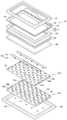
도 1 내지 도 3을 참조하여, 본 발명의 제1 실시예에 따른 액정 표시 장치에 대하여 상세히 설명한다. 도 1은 본 발명의 제1 실시예에 따른 액정 표시 장치의 분해 사시도이고, 도 2는 도 1의 액정 표시 장치 중 기판 고정부, 반사 시트 및 광원 어셈블리의 관계를 나타내는 분해 사시도이고, 도 3은 도 2의 액정 표시 장치의 단면도이다.1 to 3, a liquid crystal display according to a first embodiment of the present invention will be described in detail. FIG. 1 is an exploded perspective view of a liquid crystal display device according to a first embodiment of the present invention, FIG. 2 is an exploded perspective view showing the relationship between a substrate fixing portion, a reflection sheet and a light source assembly in the liquid crystal display device of FIG. 1, 2 is a cross-sectional view of the liquid crystal display device of Fig.
도 1을 참조하면, 본 발명의 제1 실시예에 따른 액정 표시 장치(100)는 액정 패널 어셈블리(30), 상부 수납 용기(20), 및 백라이트 어셈블리(10)를 포함한다.Referring to FIG. 1, a
액정 패널 어셈블리(30)는 하부 표시판(32), 상부 표시판(33) 및 두 표시판 사이에 개재된 액정층(미도시)을 포함하는 액정 패널(31), 게이트 테이프 캐리어 패키지(35), 데이터 테이프 캐리어 패키지(34) 및 인쇄 회로 기판(36)을 포함한다.The liquid
게이트 테이프 캐리어 패키지(35)는 하부 표시판(32)에 형성된 각 게이트 라인(미도시)에 접속되고, 데이터 테이프 캐리어 패키지(34)는 하부 표시판(32)에 형성된 각 데이터 라인(미도시)에 접속된다.The gate
한편 인쇄 회로 기판(36)에서는 게이트 테이프 캐리어 패키지(35)에 게이트 구동 신호 및 데이터 테이프 캐리어 패키지(34)에 데이터 구동 신호를 제공하는 여러 구동 부품이 실장된다.On the other hand, in the printed
그리고 백라이트 어셈블리(10)는 중간 프레임(110), 광학 시트들(120), 확산판(130), 반사 시트(140), 광원 어셈블리(150), 및 하부 수납 용기(160)를 포함한다.The backlight assembly 10 includes an
광원 어셈블리(150)는 다수의 광원 블록(150a, 150b, 150c, 150d)으로 구성된다. 각 광원 블록(150a, 150b, 150c, 150d)은 회로 패턴이 형성된 기판(152)과, 기판(152) 상에 이격되어 배치된 다수의 점광원(154)을 포함한다. 점광원(154)으로는 LED(light emitting diode) 등이 사용될 수 있다. 액정 표시 장치(100)는 전체적으로 직사각형 형상을 가진다. 액정 표시 장치(100)의 단변을 세로 방향이라 하고 장변을 가로 방향이라고 할 때, 다수의 광원 블록(150a, 150b, 150c, 150d)은 가로 방향으로 배열될 수 있다. 이 경우 광원 블록(150a, 150b, 150c, 150d) 사이의 경계부는 세로 방향으로 뻗게 된다. 각 광원 블록(150a, 150b, 150c, 150d)의 경계부에는 기판 고정부(170)가 배치되어 광원 블록(150a, 150b, 150c, 150d)을 하부 수납 용기(160)에 고정한다. 이와 같이 기판 고정부(170)는 광원 블록(150a, 150b, 150c, 150d) 사이에 배치됨으로써 광원 블록(150a, 150b, 150c, 150d)의 경계부에 암부가 생기는 것을 방지할 수 있다. 또한, 기판 고정부(170)는 상기 경계부를 균일하게 눌러서 광원 블록(150a, 150b, 150c, 150d)을 고정시킴으로써 경계부에서 기판(152)이 들뜨는 것을 방지할 수 있다. 광원 블록(150a, 150b, 150c, 150d)의 경계부의 양측에 배치된 한 쌍의 기판들(152)은 하부 수납 용기(160)에 대하여 동일한 높이에 위치할 수 있다. 기판 고정부(170)와 광원 어셈블리(150)의 관계에 대해서는 후에 자세히 설명한다.The
반사 시트(140)는 광원 어셈블리(150)의 상부에 설치되며, 광원 어셈블리(150)의 점광원(154)이 상부로 노출되도록 점광원(154)에 대응하는 다수의 개구 부(142)를 구비한다. 반사 시트(140)는 점광원(154)으로부터 방출되는 광이 확산판(130) 등에 반사되어 아래로 향할 경우 이를 상부로 반사한다. 반사 시트(140)는 광원 어셈블리(150)와 별도로 구비될 수도 있고, 광원 어셈블리(150)의 기판(152) 상부에 결합될 수도 있다. 또한 반사 시트(140)는 각 광원 블록(150a, 150b, 150c, 150d)에 대하여 하나의 시트로 형성될 수도 있고, 본 실시예와 같이 다수의 반사 블록(140a, 140b, 140c, 140d)으로 구성될 수도 있다. 예를 들어, 반사 블록(140a, 140b, 140c, 140d)이 광원 블록(150a, 150b, 150c, 150d)의 개수만큼 이루어지는 경우, 반사 블록(140a, 140b, 140c, 140d)의 경계부는 광원 블록(150a, 150b, 150c, 150d)의 경계부와 중첩될 수 있다. 본 발명의 다른 실시예로서 광원 어셈블리(150)의 기판(152)이 반사 표면을 가지는 경우, 반사 시트(140)는 생략될 수도 있다. 이하, 설명의 편의를 위하여 반사 시트(140)가 구비된 백라이트 어셈블리를 이용하여 본 발명을 설명한다.The
확산판(130)는 광원 어셈블리(150) 및 반사 시트(140)의 상부에 배치될 수 있으며, 광원 어셈블리(150)에서 발생한 광의 휘도 균일성을 향상시키는 역할을 한다. 구체적으로 확산판(130)은 점광원(154)의 배치에 따라 밝은 부분으로 나타나는 휘점이 액정 표시 장치(100)의 전면에서 보이지 않도록 한다.The
그리고 광학 시트들(120)은 확산판(130) 상부에 설치되며, 광원 어셈블리(150)로부터 전달되는 광을 확산하고 집광하는 역할을 한다. 광학 시트들(120)은 확산 시트(diffusion sheet), 제1 프리즘 시트, 제2 프리즘 시트 등을 포함한다.The
여기서 확산 시트는 광원 어셈블리(150) 상부에 위치하고 광원 어셈블 리(150)로부터 입사되는 광의 휘도 및 휘도 균일성을 향상시키는 역할을 한다. 제1 프리즘 시트는 확산 시트 상부에 위치하고, 제1 프리즘 시트의 일면에는 확산 시트로부터 확산된 광을 집광하여 출사하기 위한 삼각기둥 모양의 프리즘 패턴(미도시)이 일정한 배열을 갖고 형성되어 있다. 예를 들어, 제1 프리즘 시트로는 휘도 강화 필름(Brightness Enhancement Film)을 사용할 수 있다. 제2 프리즘 시트는 제1 프리즘 시트 상부에 위치하고, 광을 집광 및 편광하여 출사하는 다층 구조의 반사형 편광 프리즘 시트이다. 예를 들어, 제2 프리즘 시트로는 듀얼 휘도 강화 필름(Dual Brightness Enhancement Film)을 사용할 수 있다. 다만 제1 프리즘 시트만으로도 휘도 및 시야각을 충분히 확보할 수 있는 경우 제2 프리즘 시트는 제외될 수 있다.The diffusion sheet is positioned above the
중간 프레임(110)은 이러한 광학 시트들(120), 확산판(130), 반사 시트(140) 및 광원 어셈블리(150)를 수납하고, 하부 수납 용기(160)에 안착되어 고정된다. 중간 프레임(110)은 직사각형 형상의 가장자리를 따라 형성된 측벽들로 구성되고, 중앙부에 확산판(130) 및 광학 시트들(120)을 통과한 빛이 투과될 수 있도록 개방창을 구비한다.The
액정 패널 어셈블리(30)는 광학 시트들(120) 위에 설치되며, 중간 프레임(110)의 지지를 받으며 하부 수납 용기(160) 내에 안착된다. 중간 프레임(110)의 내측벽에 단차부 또는 돌기부가 형성되어 액정 패널 어셈블리(30)가 지지될 수 있다. 하부 수납 용기(160)는 직사각형 형상의 바닥부와 바닥부의 가장자리를 따라 형성된 측벽들을 포함하며, 측벽 내에 광학 시트들(120), 확산판(130), 광원 어셈블리(150), 반사 시트(140) 및 액정 패널 어셈블리(30)를 수용하여 고정시키는 역 할을 수행한다. 하부 수납 용기(160)의 바닥부에는 기판 고정부(170)가 삽입되어 고정되는 결합공(162)이 형성되어 있다. 그리고 액정 패널 어셈블리(30)의 인쇄 회로 기판(36)은 하부 수납 용기(160)의 외측벽을 따라 절곡되어 하부 수납 용기(160)의 측벽 또는 배면에 안착된다. 여기서, 광학 시트들(120), 확산판(130), 광원 어셈블리(150), 반사 시트(140) 또는 액정 패널 어셈블리(30)를 하부 수납 용기(160)에 수용하는 방법에 따라서 하부 수납 용기(160)의 형상은 다양하게 변형될 수 있다.The liquid
그리고 하부 수납 용기(160)와 결합하여 액정 패널 어셈블리(30)의 상면을 덮도록 상부 수납 용기(20)가 배치된다. 상부 수납 용기(20)의 중앙부에는 액정 패널 어셈블리(30)를 외부로 노출시키는 개방창이 형성되어 있다.The
상부 수납 용기(20)는 후크 결합 및/또는 나사 결합을 통하여 하부 수납 용기(160)와 체결될 수 있다. 이뿐만 아니라, 상부 수납 용기(20)와 하부 수납 용기(160)의 결합은 다양한 형태로 변형될 수 있다.The
도 2 및 도 3을 참조하면, 광원 어셈블리(150)는 다수의 광원 블록(150a, 150b)으로 구성되더라도, 휘도 균일성을 얻기 위하여 점광원(154)은 일정한 간격으로 이격되어 배치될 수 있다. 예를 들어, 점광원(154)은 가로 방향 및 세로 방향으로 균일한 간격으로 이격되어 매트릭스 형태로 배열될 수 있다. 또한, 점광원(154)은 세로 방향으로는 나란히 배열되고 가로 방향으로는 지그재그로 배열될 수 있다. 또한, 점광원(154)은 가로 방향으로는 나란히 배열되고 세로 방향으로는 지그재그로 배열될 수 있다. 본 발명은 이에 한정되지 않으며, 휘도 균일성을 얻기 위하여 점광원(154)은 다양하게 배열될 수 있다.2 and 3, although the
기판 고정부(170)는 광원 블록(150a, 150b)의 경계부 또는 반사 블록(140a, 140b)의 경계부를 따라 연장된 헤드(172)와, 헤드(172)의 하면으로부터 돌출된 하나 이상의 결합 돌기(174)를 포함한다. 경계부에서 암부가 형성되지 않기 위해서 헤드(172)는 높은 반사율을 가지는 것이 바람직하며, 예를 들어 반사 시트(140)의 반사율 이상의 반사율을 가질 수 있다. 헤드(172)는 반원 또는 반타원 형상의 단면을 가지므로, 헤드(172)의 상면은 전방향으로 균일하게 빛을 반사할 수 있다. 헤드(172)의 하면은 평평한 면으로 이루어지고, 반사 시트(140)의 경계부 및 광원 어셈블리(150)의 경계부를 균일한 힘으로 누르는 역할을 한다. 본 발명의 다른 실시예에 있어서, 헤드(172)는 투명한 재질로 이루어질 수도 있다. 이 경우 헤드(172)의 하면이 반사 표면으로 이루어지거나 헤드(172) 하부에 별도의 반사 부재가 추가될 수도 있다.The
결합 돌기(174)는 헤드(172)의 폭보다 좁은 폭으로 형성되며, 반사 블록(140a, 140b)의 경계부와 광원 블록(150a, 150b)의 경계부를 거쳐 하부 수납 용기(160)의 결합공(162)에 삽입되어 고정된다. 구체적으로 제1 광원 블록(150a)과 제2 광원 블록(150b)은 서로 이격되어 배치되고, 제1 반사 블록(140a)과 제2 반사 블록(140b)은 서로 이격되어 배치된다. 결합 돌기(174)는 제1 광원 블록(150a)과 제2 광원 블록(150b) 사이의 이격 공간 및 제1 반사 블록(140a)과 제2 반사 블록(140b) 사이의 이격 공간을 지나가게 된다. 따라서, 결합 돌기(174)의 폭(L3)은 제1 광원 블록(150a) 및 제2 광원 블록(150b)의 이격 거리(L1), 및 제1 반사 블 록(140a)과 제2 반사 블록(140b)의 이격 거리(L2) 보다 같거나 작은 것이 바람직하다. 또한, 헤드(172)의 폭은 이격 거리(L1) 및 이격 거리(L2) 보다 넓은 것이 바람직하다. 결합 돌기(174)의 끝단에는 결합 돌기(174)보다 폭이 넓은 걸림부(176)가 형성되어 결합 돌기(174)가 결합공(162)에 견고하게 고정될 수 있다.The coupling protrusions 174 are formed to have a width narrower than the width of the
도 3을 참조하면, 빛은 점광원(154)의 상면을 통하여 방사되므로, 헤드(172)의 높이가 점광원(154)의 높이보다 작거나 같은 것이 바람직하다. 다시 말해, 반사 블록(140a, 140b)으로부터 헤드(172)의 상부까지의 거리(H1)는 반사 블록(140a, 140b)으로부터 점광원(154) 상부까지의 거리(H2) 보다 작거나 같은 것이 바람직하다. 또한, 광원 블록(150a, 150b)의 기판(152)으로부터 헤드(172)의 상부까지의 거리는 광원 어셈블리(150)의 기판(152)으로부터 점광원(154)의 상부까지의 거리보다 작거나 같은 것이 바람직하다. 헤드(172)의 높이가 점광원(154)의 높이보다 높은 경우, 점광원(154)으로부터 방사되는 빛이 직접 헤드(172)에 닿게 되어 휘도가 불균일해 질 수 있다.3, it is preferable that the height of the
이하 도 4 내지 도 6을 참조하여, 본 발명의 기판 고정부의 변형예들을 설명한다. 여기서 도 4 내지 도 6은 본 발명의 기판 고정부의 변형예를 나타내는 단면도들이다.Modifications of the substrate fixing portion of the present invention will be described below with reference to Figs. 4 to 6. Fig. 4 to 6 are sectional views showing a modified example of the substrate fixing unit of the present invention.
도 4에 도시된 바와 같이, 기판 고정부(170a)는 삼각형 형상의 단면을 가지는 헤드(172a)와, 헤드(172a)의 하면으로부터 돌출된 하나 이상의 결합 돌기(174)를 포함한다. 바람직하게는 헤드(172a)는 이등변 삼각형 형상을 가짐으로써 양방향으로 균일한 반사율을 가질 수 있다.4, the
도 5에 도시된 바와 같이, 기판 고정부(170b)는 평판 형상의 헤드(172b)와, 헤드(172b)의 하면으로부터 돌출된 하나 이상의 결합 돌기(174)를 포함한다. 헤드(172b)의 단면은 직사각형 형상이며, 헤드(172b)의 상면은 반사 시트(140)와 평행하게 배치됨으로써, 헤드(172b)는 반사 블록(140a, 140b) 사이의 경계부를 덮으면서 반사 시트(140)와 동일한 기능을 수행할 수 있다.5, the
도 6에 도시된 바와 같이, 기판 고정부(170c)는 헤드(172)와, 헤드(172)의 하면으로부터 돌출된 하나 이상의 결합 돌기(174)와, 헤드(172) 상면에 형성된 반사 필름(172d)을 포함한다. 반사 필름(172d)은 반사 시트(140)의 반사율 이상의 반사율을 가질 수 있다. 이 경우, 헤드(172) 및 결합 돌기(174)는 반사율과 상관없이 임의의 물질로 형성될 수 있다.6, the substrate fixing portion 170c includes a
이하 도 7를 참조하여 본 발명의 제2 실시예에 따른 액정 표시 장치를 설명한다. 여기서 도 7은 본 발명의 제2 실시예에 따른 액정 표시 장치의 분해 사시도이다. 설명의 편의상, 상기 제1 실시예의 도면에 나타낸 각 부재와 동일 기능을 갖는 부재는 동일 부호로 나타내고, 따라서 그 설명은 생략하며, 이하 차이점을 위주로 설명한다.Hereinafter, a liquid crystal display according to a second embodiment of the present invention will be described with reference to FIG. 7 is an exploded perspective view of a liquid crystal display device according to a second embodiment of the present invention. For convenience of explanation, the members having the same functions as those of the members shown in the drawings of the first embodiment are denoted by the same reference numerals and the description thereof will be omitted, and the differences will be mainly described below.
도 7에 도시된 바와 같이, 광원 블록(150a, 150b, 150c, 150d)의 경계부에는 복수의 기판 고정부(170)가 일정한 간격을 두고 이격되어 배치된다. 각 기판 고정부(170)은 반사 블록(140a, 140b, 140c, 140d)의 경계부 및 광원 블록(150a, 150b, 150c, 150d)의 경계부를 거쳐 하부 수납 용기(160)의 결합공(162)에 결합된다.As shown in FIG. 7, a plurality of
이하 도 8을 참조하여 본 발명의 제3 실시예에 따른 액정 표시 장치를 설명 한다. 여기서 도 8은 본 발명의 제3 실시예에 따른 액정 표시 장치 중 기판 고정부, 반사 시트 및 광원 어셈블리의 관계를 나타내는 분해 사시도이다. 설명의 편의상, 상기 제1 실시예의 도면에 나타낸 각 부재와 동일 기능을 갖는 부재는 동일 부호로 나타내고, 따라서 그 설명은 생략하며, 이하 차이점을 위주로 설명한다.Hereinafter, a liquid crystal display according to a third embodiment of the present invention will be described with reference to FIG. 8 is an exploded perspective view showing the relationship between the substrate fixing portion, the reflection sheet, and the light source assembly in the liquid crystal display device according to the third embodiment of the present invention. For convenience of explanation, the members having the same functions as those of the members shown in the drawings of the first embodiment are denoted by the same reference numerals and the description thereof will be omitted, and the differences will be mainly described below.
도 8에 도시된 바와 같이, 제1 반사 블록(140a) 및 제2 반사 블록(140b)의 경계부에는 기판 고정부(170)의 결합 돌기(174)가 통과할 수 있는 제1 홈부(144)가 형성되어 있다. 또한, 제1 광원 블록(150a)과 제2 광원 블록(150b)의 경계부에도 기판 고정부(170)의 결합 돌기(174)가 통과할 수 있는 제2 홈부(156)가 형성되어 있다. 기판 고정부(170)의 결합 돌기(174)는 제1 홈부(144) 및 제2 홈부(156)를 통과한다.8, a
따라서, 제1 반사 블록(140a)과 제2 반사 블록(140b)이 접촉하고 제1 광원 블록(150a)과 제2 광원 블록(150b)이 접촉한 상태에서도, 기판 고정부(170)가 반사 시트(140) 및 광원 어셈블리(150)를 거쳐 하부 수납 용기(160)에 효과적으로 고정될 수 있다.Therefore, even when the first
이하 도 9 및 도 10을 참조하여 본 발명의 제4 실시예에 따른 액정 표시 장치를 설명한다. 여기서 도 9는 본 발명의 제4 실시예에 따른 액정 표시 장치 중 기판 고정부, 반사 시트 및 광원 어셈블리의 관계를 나타내는 분해 사시도이다. 도 10은 도 9의 액정 표시 장치의 단면도이다. 설명의 편의상, 상기 제1 실시예의 도면에 나타낸 각 부재와 동일 기능을 갖는 부재는 동일 부호로 나타내고, 따라서 그 설명은 생략하며, 이하 차이점을 위주로 설명한다.Hereinafter, a liquid crystal display according to a fourth embodiment of the present invention will be described with reference to FIGS. 9 and 10. FIG. 9 is an exploded perspective view showing a relationship between a substrate fixing portion, a reflection sheet, and a light source assembly in a liquid crystal display device according to a fourth embodiment of the present invention. 10 is a sectional view of the liquid crystal display device of Fig. For convenience of explanation, the members having the same functions as those of the members shown in the drawings of the first embodiment are denoted by the same reference numerals and the description thereof will be omitted, and the differences will be mainly described below.
도 9 및 도 10을 참조하면, 기판 고정부(270)는 제1 반사 블록(140a) 및 제2 반사 블록(140b)의 경계부와 제1 광원 블록(150a) 및 제2 광원 블록(150b)의 경계부를 덮는 헤드(172)와, 헤드(172)의 하면으로부터 돌출된 하나 이상의 결합 돌기(174)를 포함한다. 결합 돌기(174)는 헤드(172)의 중앙부로부터 일측으로 치우쳐 형성될 수 있다.9 and 10, the
제1 반사 블록(140a) 및 제2 반사 블록(140b)의 경계부와 인접한 제2 반사 블록(140b)의 내부에 제1 관통홀(244)이 형성된다. 제1 광원 블록(150a)과 제2 광원 블록(150b)의 경계부와 인접한 제2 광원 블록(150b)의 내부에는 제2 관통홀(256)이 형성된다. 기판 고정부(270)의 결합 돌기(174)는 제1 관통홀(244) 및 제2 관통홀(256)을 통과한다.A first through
따라서, 제1 반사 블록(140a)과 제2 반사 블록(140b)이 접촉한고 제1 광원 블록(150a)과 제2 광원 블록(150b)이 접촉한 상태에서도, 기판 고정부(270)가 반사 시트(140) 및 광원 어셈블리(150)를 거쳐 하부 수납 용기(160)에 효과적으로 고정될 수 있다.Therefore, even when the first
이하 도 11을 참조하여 본 발명의 제5 실시예에 따른 액정 표시 장치를 설명한다. 여기서 도 11은 본 발명의 제5 실시예에 따른 액정 표시 장치의 분해 사시도이다. 설명의 편의상, 상기 제1 실시예의 도면에 나타낸 각 부재와 동일 기능을 갖는 부재는 동일 부호로 나타내고, 따라서 그 설명은 생략하며, 이하 차이점을 위주로 설명한다.Hereinafter, a liquid crystal display according to a fifth embodiment of the present invention will be described with reference to FIG. 11 is an exploded perspective view of a liquid crystal display device according to a fifth embodiment of the present invention. For convenience of explanation, the members having the same functions as those of the members shown in the drawings of the first embodiment are denoted by the same reference numerals and the description thereof will be omitted, and the differences will be mainly described below.
본 실시예에서는 광원 어셈블리(250)를 구성하는 다수의 광원 블록(150a, 150b, 150c)이 세로 방향으로 배열되어 있고, 광원 블록(150a, 150b, 150c) 사이의 경계부는 가로 방향으로 뻗게 된다. 또한, 반사 시트(240)를 구성하는 다수의 반사 블록(140a, 140b, 140c)도 세로 방향으로 배열되어 있고, 반사 블록(140a, 140b, 140c) 사이의 경계부는 가로 방향으로 뻗게 된다.In this embodiment, a plurality of light source blocks 150a, 150b and 150c constituting the
광원 블록(150a, 150b, 150c)의 경계부 및 반사 블록(140a, 140b, 140c)의 경계부에는 기판 고정부(170)가 배치되어 광원 블록(150a, 150b, 150c) 및 반사 블록(140a, 140b, 140c)을 하부 수납 용기(160)에 고정한다.A
이하 도 12a 및 도 12b를 참조하여, 본 발명의 실시예들에 따른 액정 표시 장치의 휘도 균일성(brightness uniformity)에 대하여 설명한다. 도 12a는 종래 기술에 따른 액정 표시 장치의 휘도를 측정한 이미지이고, 도 12b는 본 발명에 따른 액정 표시 장치의 휘도를 측정한 이미지이다. 도 12a 및 도 12b의 이미지에 있어서 동일한 색상은 동일한 휘도를 나타낸다.Hereinafter, brightness uniformity of a liquid crystal display according to embodiments of the present invention will be described with reference to FIGS. 12A and 12B. FIG. FIG. 12A is an image obtained by measuring luminance of a liquid crystal display according to the related art, and FIG. 12B is an image illustrating luminance of a liquid crystal display according to the present invention. In the images of Figs. 12A and 12B, the same hue shows the same luminance.
도 12a의 경우 점선으로 나타낸 광원 블록의 경계부에서 휘도가 떨어지는 것이 관찰되었으나, 도 12b의 경우 광원 블록의 경계부에서도 휘도가 균일하게 나타나는 것으로 관찰되었다. 이와 같이 육안으로 경계부에서 휘도가 떨어지는 것이 관찰되는 것을 방지하기 위해서 광원 블록 내부에서의 휘도치에 대하여 광원 블록의 경계부에서의 휘도치는 2 % 이하의 차이를 가지는 것이 바람직하다. 구체적으로, 도 12a의 경우 광원 블록 내부의 휘도치가 5315 니트(nit)이고 경계부의 휘도치는 5125 니트로서 휘도차는 약 3.6%가 되어 휘선이 관찰되었다. 하지만, 도 12b의 경우 광원 블록 내부의 휘도치가 5300 니트이고 경계부의 휘도치는 5250 니트로서 휘 도차는 약 0.95%에 불과하여 경계부의 휘선이 관찰되지 않았다.In FIG. 12A, it is observed that the brightness decreases at the boundary of the light source block shown by the dotted line. In FIG. 12B, however, the brightness is uniformly seen at the boundary of the light source block. In order to prevent the brightness from being observed at the boundaries in the naked eye, it is preferable that the brightness value at the boundary of the light source block has a difference of 2% or less with respect to the brightness value in the light source block. Specifically, in FIG. 12A, the luminance value inside the light source block was 5315 knits and the luminance value at the boundary was 5125 knits, and the luminance difference was about 3.6%, and a bright line was observed. However, in the case of FIG. 12B, the luminance value inside the light source block is 5300 knits, and the luminance value at the boundary portion is 5250 knits, and the luminance difference is only about 0.95%, so that no bright line is observed at the boundary portion.
이상 첨부된 도면을 참조하여 본 발명의 실시예를 설명하였지만, 본 발명이 속하는 기술분야에서 통상의 지식을 가진 자는 본 발명이 그 기술적 사상이나 필수적인 특징을 변경하지 않고서 다른 구체적인 형태로 실시될 수 있다는 것을 이해할 수 있을 것이다. 그러므로 이상에서 기술한 실시예들은 모든 면에서 예시적인 것이며 한정적이 아닌 것으로 이해해야만 한다.While the present invention has been described in connection with what is presently considered to be practical exemplary embodiments, it is to be understood that the invention is not limited to the disclosed embodiments, but, on the contrary, You will understand. It is therefore to be understood that the above-described embodiments are illustrative in all aspects and not restrictive.
도 1은 본 발명의 제1 실시예에 따른 액정 표시 장치의 분해 사시도이다.1 is an exploded perspective view of a liquid crystal display device according to a first embodiment of the present invention.
도 2는 도 1의 액정 표시 장치 중 기판 고정부, 반사 시트 및 광원 어셈블리의 관계를 나타내는 분해 사시도이다.2 is an exploded perspective view showing the relationship between the substrate fixing portion, the reflection sheet, and the light source assembly in the liquid crystal display device of FIG.
도 3은 도 2의 액정 표시 장치의 단면도이다.3 is a sectional view of the liquid crystal display device of Fig.
도 4 내지 도 6은 본 발명의 기판 고정부의 변형예를 나타내는 단면도들이다.4 to 6 are sectional views showing a modification of the substrate fixing unit of the present invention.
도 7은 본 발명의 제2 실시예에 따른 액정 표시 장치의 분해 사시도이다.7 is an exploded perspective view of a liquid crystal display device according to a second embodiment of the present invention.
도 8은 본 발명의 제3 실시예에 따른 액정 표시 장치 중 기판 고정부, 반사 시트 및 광원 어셈블리의 관계를 나타내는 분해 사시도이다.8 is an exploded perspective view showing a relationship between a substrate fixing portion, a reflection sheet, and a light source assembly in a liquid crystal display device according to a third embodiment of the present invention.
도 9는 본 발명의 제4 실시예에 따른 액정 표시 장치 중 기판 고정부, 반사 시트 및 광원 어셈블리의 관계를 나타내는 분해 사시도이다.9 is an exploded perspective view showing the relationship between the substrate fixing portion, the reflection sheet, and the light source assembly in the liquid crystal display device according to the fourth embodiment of the present invention.
도 10은 도 9의 액정 표시 장치의 단면도이다.10 is a sectional view of the liquid crystal display device of Fig.
도 11은 본 발명의 제5 실시예에 따른 액정 표시 장치의 분해 사시도이다.11 is an exploded perspective view of a liquid crystal display device according to a fifth embodiment of the present invention.
도 12a는 종래 기술에 따른 액정 표시 장치의 휘도를 측정한 이미지이다.12A is an image obtained by measuring the luminance of a liquid crystal display according to the related art.
도 12b는 본 발명에 따른 액정 표시 장치의 휘도를 측정한 이미지이다.12B is an image obtained by measuring the luminance of the liquid crystal display device according to the present invention.
(도면의 주요부분에 대한 부호의 설명)DESCRIPTION OF THE REFERENCE NUMERALS (S)
10: 백라이트 어셈블리20: 상부 수납 용기10: backlight assembly 20: upper storage container
30: 액정 패널 어셈블리31: 액정 패널30: liquid crystal panel assembly 31: liquid crystal panel
32: 하부 표시판33: 상부 표시판32: lower panel 33: upper panel
34: 데이터 테이프 캐리어 패키지35: 게이트 테치프 캐리어 패키지34: Data Tape Carrier Package 35: Gate Tape Carrier Package
36: 인쇄 회로 기판110: 중간 프레임36: printed circuit board 110: intermediate frame
120: 광학 시트들130: 확산판120: optical sheets 130: diffuser plate
140: 반사 시트140a, 140b, 140c, 140d: 반사 블록140:
142: 개구부144: 제1 홈부142: opening 144: first groove
150: 광원 어셈블리150a, 150b, 150c, 150d: 광원 블록150:
152: 기판154: 점광원152: substrate 154: point light source
156: 제2 홈부160: 하부 수납 용기156: second groove portion 160: lower storage container
162: 결합공170: 기판 고정부162: coupling hole 170: substrate fixing portion
172: 헤드174: 결합 돌기172: head 174: engaging projection
176: 걸림부244: 제1 관통홀176: Retaining part 244: First through hole
256: 제2 관통홀256: second through hole
Claims (20)
Translated fromKoreanPriority Applications (2)
| Application Number | Priority Date | Filing Date | Title |
|---|---|---|---|
| KR1020080096634AKR101471945B1 (en) | 2008-10-01 | 2008-10-01 | Backlight assembly |
| US12/542,923US8167445B2 (en) | 2008-10-01 | 2009-08-18 | Backlight assembly |
Applications Claiming Priority (1)
| Application Number | Priority Date | Filing Date | Title |
|---|---|---|---|
| KR1020080096634AKR101471945B1 (en) | 2008-10-01 | 2008-10-01 | Backlight assembly |
Publications (2)
| Publication Number | Publication Date |
|---|---|
| KR20100037346A KR20100037346A (en) | 2010-04-09 |
| KR101471945B1true KR101471945B1 (en) | 2014-12-12 |
Family
ID=42057266
Family Applications (1)
| Application Number | Title | Priority Date | Filing Date |
|---|---|---|---|
| KR1020080096634AExpired - Fee RelatedKR101471945B1 (en) | 2008-10-01 | 2008-10-01 | Backlight assembly |
Country Status (2)
| Country | Link |
|---|---|
| US (1) | US8167445B2 (en) |
| KR (1) | KR101471945B1 (en) |
Families Citing this family (31)
| Publication number | Priority date | Publication date | Assignee | Title |
|---|---|---|---|---|
| KR101368857B1 (en)* | 2008-01-28 | 2014-02-28 | 삼성디스플레이 주식회사 | Light assembly and liquid crystal display having the same |
| JP4519944B1 (en)* | 2009-05-22 | 2010-08-04 | シャープ株式会社 | Light source device and display device |
| JP5351723B2 (en) | 2009-05-22 | 2013-11-27 | シャープ株式会社 | Light source device and display device |
| KR100939382B1 (en)* | 2009-06-24 | 2010-01-29 | (주)엘포인트 | Device for connecting a led board and chassis and back light utiling the same |
| TWM385715U (en)* | 2009-12-14 | 2010-08-01 | Chunghwa Picture Tubes Ltd | Backlight module |
| JP4781483B1 (en)* | 2010-02-26 | 2011-09-28 | シャープ株式会社 | Light guide plate device, light source device, display device, and television receiver |
| US9081227B2 (en)* | 2010-07-13 | 2015-07-14 | Sharp Kabushiki Kaisha | Lighting device having reflecting sheet and connector for fastening said reflecting sheet and display device |
| US20130148332A1 (en)* | 2010-09-15 | 2013-06-13 | Sharp Kabushiki Kaisha | Illumination device and display device |
| KR20120030802A (en)* | 2010-09-20 | 2012-03-29 | 삼성전자주식회사 | Liquid crystal display module and liquid crystal display device having the same |
| JP2012155033A (en)* | 2011-01-24 | 2012-08-16 | Panasonic Liquid Crystal Display Co Ltd | Liquid crystal display device |
| EP2696129B1 (en) | 2011-04-04 | 2019-09-04 | LG Innotek Co., Ltd. | Lighting apparatus |
| JP2012230264A (en) | 2011-04-26 | 2012-11-22 | Panasonic Liquid Crystal Display Co Ltd | Liquid crystal display device |
| WO2013031319A1 (en) | 2011-08-29 | 2013-03-07 | パナソニック液晶ディスプレイ株式会社 | Liquid-crystal display device and television receiver |
| CN102901014A (en)* | 2012-11-14 | 2013-01-30 | 深圳市华星光电技术有限公司 | Direct type backlight module and liquid crystal display module using same |
| US9482410B2 (en) | 2012-12-11 | 2016-11-01 | Samsung Electronics Co., Ltd. | Light emitting module and surface lighting device having the same |
| KR102098590B1 (en)* | 2012-12-11 | 2020-04-09 | 삼성전자주식회사 | Light source module and surface illumination apparatus having the same |
| WO2017150035A1 (en)* | 2016-03-01 | 2017-09-08 | ソニー株式会社 | Light emitting device, display apparatus, and illumination apparatus |
| JP7097812B2 (en)* | 2016-07-15 | 2022-07-08 | ソニーグループ株式会社 | Display device |
| CN106292029A (en)* | 2016-08-29 | 2017-01-04 | 合肥惠科金扬科技有限公司 | A kind of TFT LCD liquid crystal display screen display module |
| US20200133074A1 (en)* | 2017-04-27 | 2020-04-30 | Sharp Kabushiki Kaisha | Lighting device and display device |
| JP6411685B1 (en)* | 2017-10-12 | 2018-10-24 | ルーメンス カンパニー リミテッド | LED module assembly for display |
| CN110610929B (en)* | 2019-08-16 | 2021-12-03 | 武汉华星光电技术有限公司 | Backlight module |
| WO2021102727A1 (en)* | 2019-11-27 | 2021-06-03 | 京东方科技集团股份有限公司 | Driving substrate and manufacturing method therefor, light emitting substrate, and display device |
| CN111290174B (en)* | 2020-03-31 | 2022-04-08 | 武汉华星光电技术有限公司 | Lamp panel, backlight module and display device |
| CN111781764B (en)* | 2020-08-12 | 2025-07-04 | 成都京东方显示科技有限公司 | Back panel and display device |
| DE112022000775T5 (en)* | 2021-02-18 | 2023-11-09 | Lg Electronics Inc. | DISPLAY DEVICE |
| WO2022215830A1 (en)* | 2021-04-08 | 2022-10-13 | 엘지전자 주식회사 | Display device |
| EP4465123A4 (en)* | 2022-06-24 | 2025-06-18 | Samsung Electronics Co., Ltd | DISPLAY DEVICE |
| CN115202101A (en)* | 2022-07-01 | 2022-10-18 | Tcl王牌电器(惠州)有限公司 | Preparation method of backlight module, backlight module and display device |
| CN114967238B (en)* | 2022-07-26 | 2023-01-03 | 惠科股份有限公司 | Display device, backlight module and control method thereof |
| CN117496836B (en)* | 2023-02-10 | 2025-09-09 | 武汉华星光电技术有限公司 | Backlight panel |
Citations (3)
| Publication number | Priority date | Publication date | Assignee | Title |
|---|---|---|---|---|
| KR20040006324A (en)* | 2002-07-11 | 2004-01-24 | 삼성전자주식회사 | Back light assembly and liquid crystal display having the same |
| KR20070042907A (en)* | 2004-08-04 | 2007-04-24 | 소니 가부시끼 가이샤 | Backlight Device and Liquid Crystal Display |
| KR20080030188A (en)* | 2006-09-29 | 2008-04-04 | 삼성전자주식회사 | Reflective member and backlight assembly having same |
Family Cites Families (10)
| Publication number | Priority date | Publication date | Assignee | Title |
|---|---|---|---|---|
| KR101097486B1 (en)* | 2004-06-28 | 2011-12-22 | 엘지디스플레이 주식회사 | back light unit of liquid crystal display device |
| US20060087866A1 (en)* | 2004-10-22 | 2006-04-27 | Ng Kee Y | LED backlight |
| DE102005063433B4 (en)* | 2004-10-29 | 2009-11-26 | Lg Display Co., Ltd. | Backlight unit and liquid crystal display device |
| TWI262342B (en)* | 2005-02-18 | 2006-09-21 | Au Optronics Corp | Device for fastening lighting unit in backlight module |
| KR101134301B1 (en)* | 2005-02-28 | 2012-04-13 | 엘지디스플레이 주식회사 | Light Emitting Diodes back-light assembly and liquid crystal display device module using thereof |
| TWI293702B (en)* | 2005-03-17 | 2008-02-21 | Au Optronics Corp | Backlight modules |
| KR100703079B1 (en) | 2005-06-24 | 2007-04-06 | 삼성전기주식회사 | Backlight with refractive and reflective optical elements |
| KR101220204B1 (en) | 2005-12-28 | 2013-01-09 | 엘지디스플레이 주식회사 | Light Emitting Diodes back-light assembly and liquid crystal display device module using thereof |
| KR100790698B1 (en) | 2006-04-19 | 2008-01-02 | 삼성전기주식회사 | Backlight Unit for Liquid Crystal Display |
| KR20090057573A (en)* | 2007-12-03 | 2009-06-08 | 삼성전자주식회사 | Backlight unit and flat panel display device having the same |
- 2008
- 2008-10-01KRKR1020080096634Apatent/KR101471945B1/ennot_activeExpired - Fee Related
- 2009
- 2009-08-18USUS12/542,923patent/US8167445B2/ennot_activeExpired - Fee Related
Patent Citations (3)
| Publication number | Priority date | Publication date | Assignee | Title |
|---|---|---|---|---|
| KR20040006324A (en)* | 2002-07-11 | 2004-01-24 | 삼성전자주식회사 | Back light assembly and liquid crystal display having the same |
| KR20070042907A (en)* | 2004-08-04 | 2007-04-24 | 소니 가부시끼 가이샤 | Backlight Device and Liquid Crystal Display |
| KR20080030188A (en)* | 2006-09-29 | 2008-04-04 | 삼성전자주식회사 | Reflective member and backlight assembly having same |
Also Published As
| Publication number | Publication date |
|---|---|
| US8167445B2 (en) | 2012-05-01 |
| US20100079977A1 (en) | 2010-04-01 |
| KR20100037346A (en) | 2010-04-09 |
Similar Documents
| Publication | Publication Date | Title |
|---|---|---|
| KR101471945B1 (en) | Backlight assembly | |
| KR101628228B1 (en) | Backlight assembly and display device comprising the same | |
| US7758197B2 (en) | Backlight assembly and display device having the same | |
| JP5292476B2 (en) | Lighting device, display device, and television receiver | |
| US20080079865A1 (en) | Back-light assembly and liquid crystal display including the same | |
| KR20100033196A (en) | Supporting member for supporting optical member and display apparatus having the same | |
| KR101441306B1 (en) | Backlight assembly and liquid crystal display device including the same | |
| KR101836484B1 (en) | Backlgiht unit and liquid crystal display device the same | |
| JP5286417B2 (en) | Lighting device, display device, and television receiver | |
| KR101529574B1 (en) | Liquid crystal display device | |
| WO2011033895A1 (en) | Lighting device, display apparatus, and television receiver | |
| AU2010296607A1 (en) | Lighting device, display apparatus, and television receiver | |
| KR20080012702A (en) | Back light assembly and liquid crystal display including the same | |
| WO2011033896A1 (en) | Lighting device, display apparatus, and television receiver | |
| US9182537B2 (en) | Backlight unit and liquid crystal display device comprising the same | |
| WO2011148694A1 (en) | Illuminating device, display device, and television receiver | |
| CN102016391A (en) | Lighting device, display device, and television receiving device | |
| WO2011062023A1 (en) | Lighting device, display device, and television receiving device | |
| KR101803910B1 (en) | Liquid crystal display device | |
| KR20080040975A (en) | Backlight assembly and liquid crystal display including the same | |
| RU2486402C1 (en) | Illumination device, display device and television receiver | |
| KR101534082B1 (en) | Backlight assembly and liquid crystal display | |
| KR100943509B1 (en) | Backlight Unit | |
| KR20080061827A (en) | Lamp guide for liquid crystal display | |
| KR101776318B1 (en) | Backlight unit and liquid crystal display device having the same |
Legal Events
| Date | Code | Title | Description |
|---|---|---|---|
| PA0109 | Patent application | St.27 status event code:A-0-1-A10-A12-nap-PA0109 | |
| PG1501 | Laying open of application | St.27 status event code:A-1-1-Q10-Q12-nap-PG1501 | |
| R18-X000 | Changes to party contact information recorded | St.27 status event code:A-3-3-R10-R18-oth-X000 | |
| N231 | Notification of change of applicant | ||
| PN2301 | Change of applicant | St.27 status event code:A-3-3-R10-R13-asn-PN2301 St.27 status event code:A-3-3-R10-R11-asn-PN2301 | |
| A201 | Request for examination | ||
| PA0201 | Request for examination | St.27 status event code:A-1-2-D10-D11-exm-PA0201 | |
| E902 | Notification of reason for refusal | ||
| PE0902 | Notice of grounds for rejection | St.27 status event code:A-1-2-D10-D21-exm-PE0902 | |
| P11-X000 | Amendment of application requested | St.27 status event code:A-2-2-P10-P11-nap-X000 | |
| P13-X000 | Application amended | St.27 status event code:A-2-2-P10-P13-nap-X000 | |
| E701 | Decision to grant or registration of patent right | ||
| PE0701 | Decision of registration | St.27 status event code:A-1-2-D10-D22-exm-PE0701 | |
| GRNT | Written decision to grant | ||
| PR0701 | Registration of establishment | St.27 status event code:A-2-4-F10-F11-exm-PR0701 | |
| PR1002 | Payment of registration fee | St.27 status event code:A-2-2-U10-U11-oth-PR1002 Fee payment year number:1 | |
| PG1601 | Publication of registration | St.27 status event code:A-4-4-Q10-Q13-nap-PG1601 | |
| R18-X000 | Changes to party contact information recorded | St.27 status event code:A-5-5-R10-R18-oth-X000 | |
| LAPS | Lapse due to unpaid annual fee | ||
| PC1903 | Unpaid annual fee | St.27 status event code:A-4-4-U10-U13-oth-PC1903 Not in force date:20171206 Payment event data comment text:Termination Category : DEFAULT_OF_REGISTRATION_FEE | |
| PC1903 | Unpaid annual fee | St.27 status event code:N-4-6-H10-H13-oth-PC1903 Ip right cessation event data comment text:Termination Category : DEFAULT_OF_REGISTRATION_FEE Not in force date:20171206 | |
| R18-X000 | Changes to party contact information recorded | St.27 status event code:A-5-5-R10-R18-oth-X000 |