KR101471262B1 - Copyback optimization for memory system - Google Patents
Copyback optimization for memory systemDownload PDFInfo
- Publication number
- KR101471262B1 KR101471262B1KR1020127013247AKR20127013247AKR101471262B1KR 101471262 B1KR101471262 B1KR 101471262B1KR 1020127013247 AKR1020127013247 AKR 1020127013247AKR 20127013247 AKR20127013247 AKR 20127013247AKR 101471262 B1KR101471262 B1KR 101471262B1
- Authority
- KR
- South Korea
- Prior art keywords
- data page
- register
- volatile memory
- metadata
- memory
- Prior art date
- Legal status (The legal status is an assumption and is not a legal conclusion. Google has not performed a legal analysis and makes no representation as to the accuracy of the status listed.)
- Expired - Fee Related
Links
Images


Classifications
- G—PHYSICS
- G06—COMPUTING OR CALCULATING; COUNTING
- G06F—ELECTRIC DIGITAL DATA PROCESSING
- G06F11/00—Error detection; Error correction; Monitoring
- G06F11/07—Responding to the occurrence of a fault, e.g. fault tolerance
- G06F11/08—Error detection or correction by redundancy in data representation, e.g. by using checking codes
- G06F11/10—Adding special bits or symbols to the coded information, e.g. parity check, casting out 9's or 11's
- G06F11/1008—Adding special bits or symbols to the coded information, e.g. parity check, casting out 9's or 11's in individual solid state devices
- G06F11/1068—Adding special bits or symbols to the coded information, e.g. parity check, casting out 9's or 11's in individual solid state devices in sector programmable memories, e.g. flash disk
- G—PHYSICS
- G11—INFORMATION STORAGE
- G11C—STATIC STORES
- G11C16/00—Erasable programmable read-only memories
- G11C16/02—Erasable programmable read-only memories electrically programmable
- G11C16/06—Auxiliary circuits, e.g. for writing into memory
- G—PHYSICS
- G06—COMPUTING OR CALCULATING; COUNTING
- G06F—ELECTRIC DIGITAL DATA PROCESSING
- G06F11/00—Error detection; Error correction; Monitoring
- G06F11/07—Responding to the occurrence of a fault, e.g. fault tolerance
- G06F11/08—Error detection or correction by redundancy in data representation, e.g. by using checking codes
- G06F11/10—Adding special bits or symbols to the coded information, e.g. parity check, casting out 9's or 11's
Landscapes
- Engineering & Computer Science (AREA)
- Theoretical Computer Science (AREA)
- Quality & Reliability (AREA)
- Physics & Mathematics (AREA)
- General Engineering & Computer Science (AREA)
- General Physics & Mathematics (AREA)
- Techniques For Improving Reliability Of Storages (AREA)
- Exchange Systems With Centralized Control (AREA)
Abstract
Translated fromKorean
Description
Translated fromKorean본 발명은 일반적으로 메모리 시스템들에 관한 것이다.The present invention relates generally to memory systems.
플래쉬 메모리는, 전기적으로 소거가능한 프로그램가능 판독전용 메모리(EEPROM)의 한 종류이다. 플래쉬 메모리들은 비휘발성이고 비교적 고밀도이므로, 핸드헬드 컴퓨터, 모바일 폰, 디지털 카메라, 휴대용 음악 플레이어, 및 다른 저장 솔루션들(예컨대, 자기 디스크)이 부적절한 많은 다른 장치들의 파일들 및 다른 지속적 객체들을 저장하는데 사용된다. 플래쉬 메모리에 저장된 데이터가 처리될 때, 데이터 페이지가 플래쉬 메모리로부터 판독되어 레지스터에 저장된다. 레지스터의 콘텐트들은, 처리를 위하여 비휘발성 메모리의 외부에 있는 제어기로 전송된다. 처리된 데이터 페이지는, 처리된 데이터 페이지가 플래쉬 메모리에 다시 기록될 수 있도록 레지스터에 되돌려진다.Flash memory is one type of electrically erasable programmable read only memory (EEPROM). Because flash memories are non-volatile and relatively dense, they store files of other handheld computers, mobile phones, digital cameras, portable music players, and many other devices that are inappropriate for other storage solutions (e.g. magnetic disks) and other persistent objects Is used. When the data stored in the flash memory is processed, the data page is read from the flash memory and stored in the register. The contents of the register are transferred to a controller external to the non-volatile memory for processing. The processed data page is returned to the register so that the processed data page can be written back to the flash memory.
비휘발성 메모리 서브시스템의 카피백 또는 판독 동작에서, 데이터 페이지 변경 인디케이터들은, 비휘발성 메모리의 레지스터와 비휘발성 메모리 외부에 있는 제어기 간에 데이터 페이지들을 전송하는 것을 관리하는데 사용된다.In a copyback or read operation of a non-volatile memory subsystem, data page change indicators are used to manage transferring data pages between a register in the non-volatile memory and a controller external to the non-volatile memory.
레지스터(110)의 모든 콘텐트들이 외부 제어기(116)에 전송되는 것을 피함으로써, 처리 시간 및 전력 소비가 감소될 수 있다.By avoiding all the contents of the
도 1a는, 최적화된 카피백 프로세스를 구현하는 예시적인 메모리 시스템의 블록도이다.
도 1b는. 최적화된 카피백 프로세스를 구현하는 또 다른 예시적인 메모리 시스템의 블록도이다.
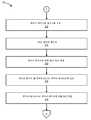
도 2는, 도 1a와 도 1b의 메모리 시스템들에 의해 사용되는 데이터 변경 인디케이터들을 계산하고 저장하기 위한 예시적인 최적화된 카피백 프로세스(200)의 흐름도이다.
도 3a 내지 도 3c는, 도 1a와 도 1b의 메모리 시스템들에 의해 구현되는 예시적인 최적화된 카피백 프로세스의 흐름도들이다.
도 4는, 도 1a와 도 1b의 메모리 시스템들에 의해 구현되는 예시적인 최적화된 판독 동작의 흐름도이다.
도 5는, 도 3a 내지 도 3c의 카피백 프로세스에 의해 사용되는 예시적인 데이터 구조들을 도시한다.1A is a block diagram of an exemplary memory system that implements an optimized copyback process.
FIG. / RTI > is a block diagram of another exemplary memory system implementing an optimized copyback process.
FIG. 2 is a flow diagram of an exemplary optimized
Figures 3A-3C are flow diagrams of an exemplary optimized copyback process implemented by the memory systems of Figures 1A and 1B.
FIG. 4 is a flow diagram of an exemplary optimized read operation implemented by the memory systems of FIGS. 1A and 1B.
Figure 5 illustrates exemplary data structures used by the copyback process of Figures 3A-3C.
메모리 서브시스템들의 예들Examples of memory subsystems
도 1a는, 최적화된 카피백 프로세스를 구현하기 위한 예시적인 메모리 시스템(100)의 블록도이다. 일부 구현예들에서, 시스템(100)은, 외부 버스(122)(예컨대, ONFI(Open NAND Flash Interface), ATA)를 통해 호스트 디바이스(124)에 결합되는 메모리 서브시스템(102)을 포함할 수 있다. 호스트 디바이스(124)는, 스마트 폰, 미디어 플레이어, 텍스트 메시징 디바이스, 휴대용 컴퓨터, 솔리드 스테이트 드라이브(solid state drive), 디지털 카메라 등이 포함되는 임의의 전자 장치일수 있으나, 이들로만 제한되는 것은 아니다. 메모리 서브시스템(102)은, 임의의 비휘발성 메모리 서브시스템(예컨대, 매니지드 낸드(managed NAND))일 수 있다.1A is a block diagram of an
호스트 디바이스(124)는, 시스템-온-칩(SoC)(126) 및 휘발성 메모리(128)를 포함할 수 있다. SoC(126)는, 호스트 디바이스(124)에서 실행되는 애플리케이션들에 의해 행해지는 판독 및 기록 요청들을 전송하는 것과 같이, 메모리 서브시스템(102)와 상호작용하기 위한 하드웨어와 소프트웨어를 포함할 수 있다.The
메모리 서브시스템(102)은, 비휘발성 메모리(104)("로우 메모리(raw memory)"라고도 칭해짐) 및 외부 제어기(116)를 포함할 수 있다. 메모리(104)는, 메모리 셀 어레이(106), 내부 상태 머신(108), 메모리 레지스터(110) 및 데이터 변경 인디케이터(DCI)(130)를 포함할 수 있다. 제어기(116)는, 프로세서(118), 휘발성 메모리(114) 및 에러 정정 코드(ECC) 엔진(120)을 포함할 수 있다. 메모리 서브시스템(102)에 대한 다른 구성들도 가능하다. 예를 들면, 캐쉬 레지스터는, 현재의 페이지가 내부 버스(112)를 통해 제어기(116)로 전송되는 동안, 내부 상태 머신이 메모리 셀 어레이(106)로부터 다음번 데이터 페이지를 판독하게 하기 위해, 메모리 셀 어레이(106) 및 메모리 레지스터(110) 사이의 데이터 경로 내에 포함될 수 있다.
도 1b는, 최적화된 카피백 프로세스를 구현하기 위한 또 다른 예시적인 메모리 시스템(130)의 블록도이다. 시스템(130)은, 메모리 서브시스템(102)만을 나타내며, 그 동작은 도 1a와 관련하여 기술되었다.1B is a block diagram of another
카피백 동작들Copyback operations
카피백은, 한 페이지에서 다른 페이지로 데이터를 옮기라는 메모리 서브시스템 커맨드일수 있다. 카피백은, 웨어 레벨링(wear leveling) 및 다른 비휘발성 메모리 관리 동작들에서 사용될 수 있다. 통상의 카피백 동작에서, 데이터 페이지는, 메모리 셀 어레이(106)로부터 판독되어, 내부 상태 머신에 의해 메모리 레지스터(110)에 저장된다. 외부 제어기(116)는, 프로세서(118)가 데이터 페이지에 대해 원하는 연산(예컨대, ECC 연산)을 수행할 수 있도록, 메모리 레지스터(110)로부터 데이터 페이지를 판독하거나, 클로킹한다. 처리된 데이터 페이지는, 제어기(116)에 의해 메모리 레지스터(110)에 다시 기록될 수 있다. 내부 상태 머신(108)은, 메모리 레지스터(110)의 콘텐트들을 메모리 셀 어레이(106) 내의 새로운 데이터 페이지에 기록할 수 있다. 레지스터(110)의 모든 콘텐트들이 외부 제어기(116)에 전송되는 것을 피함으로써, 처리 시간 및 전력 소비가 감소될 수 있다.A copyback can be a memory subsystem command to transfer data from one page to another. Copybacks can be used in wear leveling and other non-volatile memory management operations. In a normal copyback operation, the data page is read from the
새로운 데이터 페이지들의 기록에 대한 예시적인 프로세스An exemplary process for recording new data pages
도 2는, 도 1a와 도 1b의 메모리 시스템들에 의해 사용되는 데이터 변경 인디케이터들을 계산하고 저장하기 위한 예시적인 최적화된 카피백 프로세스(200)의 흐름도이다. 일부 구현예들에서, 프로세스(200)는, 새로운 데이터 페이지가 메모리 서브시스템의 메모리 레지스터 내로 전송될 때 시작될 수 있다(단계 202). 데이터 페이지에 대한 DCI가 계산되어, 메모리 서브시스템에 저장될 수 있다(단계 204). 데이터 변경 인디케이터들의 일부 예들에는, 체크섬, 해밍 코드, 패리티 비트, CRC(cyclic redundancy check), 폴래러티 심볼 리버설(polarity symbol reversal), 터보 코드 등을 비롯하여 (이들로만 제한되지는 않음) 에러 검출 코드들(EDCs)이포함될 수 있다. EDC는, 리드-솔로몬(Reed-Solomon) 코드, 리드-뮬러(Reed-Muller) 코드, 바이너리 골레이(Binary Golay) 코드, 및 저-밀도 패리티-체크 코드(low-density parity-check codes)들과 같이, ECC의 일부일 수도 있다. DCI들이 계산되고 저장된 후에, 레지스터의 콘텐트들은 비휘발성 메모리에 기록될 수 있다(단계 206). DCI들은, 도 3a 내지 도 3c와 관련하여 기술된, 최적화된 카피백 프로세스에 사용될 수 있다.FIG. 2 is a flow diagram of an exemplary optimized
최적화된 카피백 프로세스의 예Example of an Optimized Copyback Process
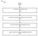
도 3a 내지 도 3c는, 도 1a와 도 1b의 메모리 시스템들에 의해 구현되는 예시적인 최적화된 카피백 프로세스(300)의 흐름도들이다. 일부 구현예들에서, 프로세스(300)는, 비휘발성 메모리(예컨대, 메모리 셀 어레이(106))로부터 데이터 페이지를 판독하고 메모리 레지스터(예컨대, 레지스터(110))에 데이터 페이지를 저장함으로써 시작될 수 있다(단계 302). DCI(예컨대, DCI(130))는, 메모리 레지스터의 데이터 페이지를 위해 검증될 수 있다(단계 304). 일부 구현예들에서, DCI는, 데이터 페이지가 (예컨대, 프로세스(200)를 이용하여) 비휘발성 메모리에 최초로 기록되는 경우, 미리 계산되어 메모리 서브시스템에 저장될 수 있다. 다른 구현예들에서, DCI는, 판독 동작의 일부로서 또는 별개의 동작으로서 "온 더 플라이(on the fly)"로 계산될 수 있다. 메모리 서브시스템은, 판독 동작이 완료되었다는 것을 외부 제어기(예컨대, 외부 제어기(116)에 보고할 수 있다(단계 306).Figures 3A-3C are flow diagrams of an exemplary optimized
레지스터의 데이터 페이지에 대한 DCI가, 데이터 페이지가 변경되었다는 것을 가리킨다면(단계 308), 데이터 페이지가 외부 제어기로 전송될 수 있고(단계 310), ECC가 데이터 페이지에 대해 계산될 수 있으며(단계 312), 그리고 데이터 페이지에 대한 ECC 정보가 외부 제어기에서 정정될 수 있다(단계 314). 데이터 페이지 및 연관된 ECC는, 메모리 레지스터로 다시 전송될 수 있다(단계 316). 새로운 DCI가, 메모리 레지스터의 데이터 페이지에 대해 계산될 수 있다(단계 318).If the DCI for the data page of the register indicates that the data page has changed (step 308), the data page may be sent to the external controller (step 310) and the ECC may be calculated for the data page (step 312 ), And the ECC information for the data page may be corrected in the external controller (step 314). The data page and the associated ECC may be sent back to the memory register (step 316). A new DCI may be computed for the data page of the memory register (step 318).
레지스터의 데이터 페이지에 대한 DCI가, 데이터 페이지가 변경되지 않았다는 것을 가리킨다면(단계 308), 데이터 페이지와 연관된 새로운 메타데이터에 대한 ECC가 계산될 수 있다(단계 320). 새로운 메타데이터 및 연관된 ECC는, 메모리 레지스터로 전송될 수 있다(단계 322). 메모리 레지스터의 메타데이터에 대한 새로운 DCI가 계산될 수 있다(단계 324). 메모리 레지스터의 콘텐트들은, 비휘발성 메모리의 새로운 데이터 페이지에 기록될 수 있다(단계 326).If the DCI for the data page of the register indicates that the data page has not changed (step 308), the ECC for the new metadata associated with the data page may be calculated (step 320). The new metadata and associated ECC may be transferred to the memory register (step 322). A new DCI for the metadata of the memory register may be calculated (step 324). The contents of the memory register may be written to a new data page of the non-volatile memory (step 326).
최적화된 판독 동작Optimized Read Operation
도 4는, 도 1a와 도 1b의 메모리 시스템들에 의해 구현되는 예시적인 최적화된 판독 동작의 흐름도이다. 일부 구현예들에서, 프로세스(400)는, 비휘발성 메모리로부터 데이터 페이지를 판독하고 메모리 레지스터에 데이터 페이지를 저장함으로써 시작될 수 있다(단계 402). 데이터 페이지와 연관되는 미리 계산된 DCI는, 메모리 서브시스템의 저장 위치로부터 메모리 레지스터 내로 클록킹되어 검증될 수 있다(단계 404). DCI는 또한 "온 더 플라이"로 계산될 수 있다. DCI의 상태가, 데이터 페이지가 변경되었는지를 판정하기 위하여 판독될 수 있다(단계 406).FIG. 4 is a flow diagram of an exemplary optimized read operation implemented by the memory systems of FIGS. 1A and 1B. In some implementations, the
데이터 페이지가 변경되었다면(단계 408), 데이터 페이지와 연관된 새 메타데이터에 대한 ECC가 계산되어, 새 메타데이터와 함께 메모리 레지스터로 전송될 수 있다(단계 412). 메모리 레지스터의 메타데이터에 대한 새로운 DCI가 계산될 수 있고, 레지스터의 콘텐트들이 비휘발성 메모리의 새로운 데이터 페이지에 기록될 수 있다(단계 414).If the data page has changed (step 408), the ECC for the new metadata associated with the data page may be computed and sent to the memory register with the new metadata (step 412). A new DCI for the metadata of the memory register may be computed and the contents of the register may be written to a new data page of the non-volatile memory (step 414).
데이터 페이지가 변경되지 않았다면(단계 408), 메모리 레지스터의 콘텐트들은 외부 제어기로 전송될 수 있고, ECC는 외부 제어기에 의해 계산될 수 있다(단계 410). 데이터 페이지와 연관된 새 메타데이터에 대한 ECC가 계산되어, 외부 제어기에 의해 새 메타데이터와 함께 메모리 레지스터로 전송될 수 있다(단계 412). 메모리 레지스터의 메타데이터에 대한 새 DCI가 계산될 수 있고, 레지스터의 콘텐트들은 비휘발성 메모리의 새 데이터 페이지에 기록될 수 있다(단계 414).If the data page has not changed (step 408), the contents of the memory register may be transferred to the external controller, and the ECC may be calculated by the external controller (step 410). The ECC for the new metadata associated with the data page may be calculated and transmitted by the external controller to the memory register along with the new metadata (step 412). A new DCI for the metadata of the memory register may be computed and the contents of the register may be written to the new data page of the non-volatile memory (step 414).
데이터 구조들의 예Examples of Data Structures
도 5는, 도 3a 내지 도 3c의 카피백 프로세스에 의해 사용되는 예시적인 데이터 구조들을 도시한다. 도시된 예에서, 비휘발성 메모리의 데이터 페이지(500)에는, 메타데이터(502), 메타데이터 ECC(504), 데이터(506) 및 데이터 ECC(508)가포함된다. 데이터가 변경되지 않았다면, 메타데이터(502)와 메타데이터 ECC(504) 만이 처리를 위해 레지스터에서 외부 제어기(510)로 전송된다. 처리된 메타데이터(502) 및 메타데이터 ECC(504)는, 메모리 서브시스템으로 다시 전송되어, 메모리 레지스터에 저장된다. 그 후에, 데이터 페이지는, 비휘발성 메모리(예컨대, 메모리 셀 어레이)의 새 데이터 페이지에 기록될 수 있다.Figure 5 illustrates exemplary data structures used by the copyback process of Figures 3A-3C. In the illustrated example,
많은 구현예들이 기술되었다. 그럼에도, 다양한 변경들이 행해질 수 있다는 것이 이해될 것이다. 예를 들면, 하나 이상의 구현예들의 엘리먼트들은, 결합되거나, 생략되거나, 변경되거나, 또는 추가적인 구현예들을 형성하도록 보충될 수 있다. 또 다른 예들에서와 같이, 도면들에 도시된 논리 흐름들은, 원하는 결과들을 달성하기 위해, 도시된 특정 순서 또는 순차적인 순서를 요구하지 않는다. 또한, 다른 단계들이 제공될 수 있고, 또는 기술된 흐름들에서 단계들이 제거될 수 있으며, 다른 컴포넌트들이 기술된 시스템들에 첨가되거나 제거될 수 있다. 따라서, 다른 구현예들은, 다음의 청구항들의 범위 내에 있게 된다.Many implementations have been described. Nevertheless, it will be understood that various modifications may be made. For example, elements of one or more embodiments may be combined, omitted, altered, or supplemented to form additional embodiments. As in other examples, the logic flows depicted in the Figures do not require the specific sequence or sequential order shown to achieve the desired results. In addition, other steps may be provided, or steps may be removed in the described flows, and other components may be added or removed from the described systems. Accordingly, other implementations are within the scope of the following claims.
100: 메모리 시스템
102: 메모리 서브시스템
104: 비휘발성 메모리
106: 메모리 셀 어레이
108: 내부 상태 머신
110: 메모리 레지스터
112: 내부 버스
114: 휘발성 메모리
116: 외부 제어기
118: 프로세서
120: 에러 정정 코드(ECC) 엔진
122: 외부 버스
124: 호스트 디바이스
126: 시스템-온-칩(SoC)
128: 휘발성 메모리
130: 데이터 변경 인디케이터(DCI)100: Memory system
102: memory subsystem
104: Nonvolatile memory
106: memory cell array
108: Internal state machine
110: memory register
112: internal bus
114: volatile memory
116: External controller
118: Processor
120: Error Correction Code (ECC) engine
122: External bus
124: Host device
126: System-on-Chip (SoC)
128: volatile memory
130: Data Change Indicator (DCI)
Claims (15)
Translated fromKorean비휘발성 메모리에 의해, 데이터 페이지를 수신하는 단계 - 상기 데이터 페이지는 데이터, 메타데이터, 상기 데이터에 대한 에러 정정 코드(Error Correction Code) 및 상기 메타데이터에 대한 에러 정정 코드를 포함함 - ;
상기 비휘발성 메모리에 의해, 상기 데이터 페이지를 레지스터 내에 저장하는 단계;
상기 비휘발성 메모리에 의해, 상기 데이터 페이지에 대한 데이터 변경 인디케이터(data change indicator)를 계산하는 단계;
상기 비휘발성 메모리에 의해, 상기 데이터 변경 인디케이터를 저장하는 단계;
상기 비휘발성 메모리에 의해, 상기 레지스터의 내용을 상기 비휘발성 메모리의 제1 위치에 기록하는 단계;
상기 비휘발성 메모리에 의해, 상기 데이터 페이지를 상기 비휘발성 메모리의 상기 제1 위치로부터 획득하는 단계;
상기 비휘발성 메모리에 의해, 상기 획득된 데이터 페이지를 상기 레지스터에 저장하는 단계;
상기 비휘발성 메모리에 의해, 상기 획득된 데이터 페이지가 변경되었는지 여부를 판정하는 단계;
상기 비휘발성 메모리에 의해, 상기 획득된 데이터 페이지가 변경되었다는 판정에 응답하여 상기 획득된 데이터 페이지를 제어기로 전송하는 단계;
상기 비휘발성 메모리에 의해, 상기 획득된 데이터 페이지가 변경되지 않았다는 판정에 응답하여 상기 획득된 데이터 페이지의 메타데이터를 상기 제어기로 전송하는 단계;
상기 제어기에 의해, 상기 획득된 데이터 페이지를 처리하는 단계;
상기 제어기에 의해, 상기 획득된 데이터 페이지의 상기 메타데이터를 처리하는 단계;
상기 제어기에 의해, 상기 레지스터의 내용을 상기 처리된 데이터 페이지로 갱신하는 단계;
상기 제어기에 의해, 상기 레지스터의 내용을 상기 처리된 메타데이터로 갱신하는 단계; 및
상기 비휘발성 메모리에 의해, 상기 레지스터의 갱신된 내용을 상기 비휘발성 메모리의 제2 위치에 기록하는 단계
를 포함하는, 방법.A method for performing a copyback operation on a memory subsystem, the method comprising:
Receiving a data page by a non-volatile memory, the data page including data, metadata, an error correction code for the data, and an error correction code for the metadata;
Storing, by the non-volatile memory, the data page in a register;
Calculating, by the non-volatile memory, a data change indicator for the data page;
Storing, by the non-volatile memory, the data change indicator;
Writing, by the non-volatile memory, the contents of the register to a first location of the non-volatile memory;
Obtaining, by the non-volatile memory, the data page from the first location of the non-volatile memory;
Storing, by the non-volatile memory, the obtained data page in the register;
Determining, by the non-volatile memory, whether the obtained data page has been changed;
Transmitting, by the non-volatile memory, the obtained data page to the controller in response to determining that the obtained data page has been changed;
Transmitting, by the non-volatile memory, the metadata of the obtained data page to the controller in response to determining that the obtained data page has not been changed;
Processing the obtained data page by the controller;
Processing, by the controller, the metadata of the obtained data page;
Updating, by the controller, the contents of the register to the processed data page;
Updating, by the controller, the content of the register with the processed metadata; And
Writing, by the non-volatile memory, the updated contents of the register to a second location of the non-volatile memory
/ RTI >
제어기; 및
메모리 어레이와 레지스터를 포함하는 비휘발성 메모리
를 포함하고,
상기 비휘발성 메모리는,
데이터 페이지를 수신하고 - 상기 데이터 페이지는 데이터, 메타데이터, 상기 데이터에 대한 에러 정정 코드 및 상기 메타데이터에 대한 에러 정정 코드를 포함함 -,
상기 데이터 페이지를 상기 레지스터에 저장하고,
상기 데이터 페이지에 대한 데이터 변경 인디케이터를 생성하고,
상기 데이터 변경 인디케이터를 저장하고,
상기 레지스터의 내용을 상기 메모리 어레이 내의 제1 위치에 기록하고,
상기 데이터 페이지를 상기 메모리 어레이의 상기 제1 위치로부터 획득하고,
상기 획득된 데이터 페이지를 상기 레지스터 내에 저장하고,
상기 획득된 데이터 페이지가 변경되었는지를 판정하고,
상기 획득된 데이터 페이지가 변경되었다는 판정에 응답하여 상기 획득된 데이터 페이지를 상기 제어기로 전송하고,
상기 획득된 데이터 페이지가 변경되지 않았다는 판정에 응답하여 상기 획득된 데이터 페이지의 메타데이터를 상기 제어기로 전송하도록 구성되고,
상기 제어기는,
상기 획득된 데이터 페이지를 처리하고,
상기 획득된 데이터 페이지의 상기 메타데이터를 처리하고,
상기 레지스터의 내용을 상기 처리된 데이터 페이지로 갱신하고,
상기 레지스터의 내용을 상기 처리된 메타데이터로 갱신하도록 구성되고,
상기 비휘발성 메모리는 상기 레지스터의 갱신된 내용을 상기 메모리 어레이의 제2 위치에 기록하도록 더 구성되는,
장치.An apparatus for performing a copyback operation,
A controller; And
A nonvolatile memory including a memory array and a register
Lt; / RTI >
The non-
Receiving a data page, the data page including data, metadata, an error correction code for the data, and an error correction code for the metadata,
Storing the data page in the register,
Generating a data change indicator for the data page,
Storing the data change indicator,
Write the contents of the register to a first location in the memory array,
Obtaining the data page from the first location of the memory array,
Storing the obtained data page in the register,
Determining whether the obtained data page has been changed,
Sending the obtained data page to the controller in response to determining that the obtained data page has been changed,
And to transmit the metadata of the obtained data page to the controller in response to determining that the obtained data page has not been changed,
The controller comprising:
Processing the obtained data page,
Processing the metadata of the obtained data page,
Updating the contents of the register to the processed data page,
And update the contents of the register with the processed metadata,
Wherein the non-volatile memory is further configured to write the updated contents of the register to a second location of the memory array,
Device.
데이터 페이지를 수신하기 위한 수단 - 상기 데이터 페이지는 데이터, 메타데이터, 상기 데이터에 대한 에러 정정 코드 및 상기 메타데이터에 대한 에러 정정 코드를 포함함 - ;
상기 데이터 페이지를 상기 메모리 서브시스템의 비휘발성 메모리의 레지스터 내에 저장하기 위한 수단;
상기 데이터 페이지에 대한 데이터 변경 인디케이터를 계산하기 위한 수단;
상기 데이터 변경 인디케이터를 저장하기 위한 수단;
상기 데이터 페이지를 상기 비휘발성 메모리의 제1 위치에 기록하기 위한 수단;
상기 데이터 페이지를 상기 비휘발성 메모리의 상기 제1 위치로부터 획득하기 위한 수단;
상기 획득된 데이터 페이지를 상기 레지스터 내에 저장하기 위한 수단;
상기 획득된 데이터 페이지가 변경되었는지 여부를 판정하기 위한 수단;
상기 획득된 데이터 페이지가 변경되었다는 판정에 응답하여 상기 획득된 데이터 페이지를 제어기로 전송하기 위한 수단;
상기 획득된 데이터 페이지가 변경되지 않았다는 판정에 응답하여 상기 획득된 데이터 페이지의 메타데이터를 상기 제어기로 전송하기 위한 수단;
상기 전송된 데이터 페이지를 처리하기 위한 수단;
상기 전송된 메타데이터를 처리하기 위한 수단;
상기 처리된 데이터 페이지를 수신하기 위한 수단;
상기 데이터 페이지의 상기 처리된 메타데이터를 수신하기 위한 수단;
상기 레지스터의 내용을 상기 처리된 데이터 페이지로 갱신하기 위한 수단;
상기 레지스터의 내용을 상기 데이터 페이지의 상기 처리된 메타데이터로 갱신하기 위한 수단; 및
상기 레지스터의 갱신된 내용을 상기 비휘발성 메모리의 제2 위치에 기록하기 위한 수단;
을 포함하는 메모리 서브시스템.As a memory subsystem,
Means for receiving a data page, the data page comprising data, metadata, an error correction code for the data and an error correction code for the metadata;
Means for storing the data page in a register of a non-volatile memory of the memory subsystem;
Means for calculating a data change indicator for the data page;
Means for storing the data change indicator;
Means for writing the data page to a first location in the non-volatile memory;
Means for obtaining the data page from the first location of the non-volatile memory;
Means for storing the obtained data page in the register;
Means for determining whether the obtained data page has changed;
Means for sending the obtained data page to a controller in response to determining that the obtained data page has changed;
Means for transmitting metadata of the obtained data page to the controller in response to determining that the obtained data page has not been changed;
Means for processing the transmitted data page;
Means for processing the transmitted metadata;
Means for receiving the processed data page;
Means for receiving the processed metadata of the data page;
Means for updating the contents of the register with the processed data page;
Means for updating the contents of the register with the processed metadata of the data page; And
Means for writing updated contents of the register to a second location of the non-volatile memory;
≪ / RTI >
Applications Claiming Priority (5)
| Application Number | Priority Date | Filing Date | Title |
|---|---|---|---|
| US4933008P | 2008-04-30 | 2008-04-30 | |
| US61/049,330 | 2008-04-30 | ||
| US12/193,638 | 2008-08-18 | ||
| US12/193,638US8185706B2 (en) | 2008-04-30 | 2008-08-18 | Copyback optimization for memory system |
| PCT/US2009/039160WO2009134576A1 (en) | 2008-04-30 | 2009-04-01 | Copyback optimization for memory system |
Related Parent Applications (1)
| Application Number | Title | Priority Date | Filing Date |
|---|---|---|---|
| KR1020107026742ADivisionKR101225924B1 (en) | 2008-04-30 | 2009-04-01 | Copyback optimization for memory system |
Publications (2)
| Publication Number | Publication Date |
|---|---|
| KR20120059658A KR20120059658A (en) | 2012-06-08 |
| KR101471262B1true KR101471262B1 (en) | 2014-12-10 |
Family
ID=40801795
Family Applications (2)
| Application Number | Title | Priority Date | Filing Date |
|---|---|---|---|
| KR1020127013247AExpired - Fee RelatedKR101471262B1 (en) | 2008-04-30 | 2009-04-01 | Copyback optimization for memory system |
| KR1020107026742AExpired - Fee RelatedKR101225924B1 (en) | 2008-04-30 | 2009-04-01 | Copyback optimization for memory system |
Family Applications After (1)
| Application Number | Title | Priority Date | Filing Date |
|---|---|---|---|
| KR1020107026742AExpired - Fee RelatedKR101225924B1 (en) | 2008-04-30 | 2009-04-01 | Copyback optimization for memory system |
Country Status (8)
| Country | Link |
|---|---|
| US (2) | US8185706B2 (en) |
| EP (2) | EP2297642B1 (en) |
| JP (1) | JP5192587B2 (en) |
| KR (2) | KR101471262B1 (en) |
| CN (1) | CN102077176B (en) |
| AT (1) | ATE535866T1 (en) |
| ES (1) | ES2378371T3 (en) |
| WO (1) | WO2009134576A1 (en) |
Families Citing this family (81)
| Publication number | Priority date | Publication date | Assignee | Title |
|---|---|---|---|---|
| US8762620B2 (en) | 2007-12-27 | 2014-06-24 | Sandisk Enterprise Ip Llc | Multiprocessor storage controller |
| US8443263B2 (en)* | 2009-12-30 | 2013-05-14 | Sandisk Technologies Inc. | Method and controller for performing a copy-back operation |
| US8365041B2 (en) | 2010-03-17 | 2013-01-29 | Sandisk Enterprise Ip Llc | MLC self-raid flash data protection scheme |
| KR101844346B1 (en)* | 2010-11-05 | 2018-04-02 | 삼성전자주식회사 | Memory system and method of operating a memory system |
| US8909982B2 (en) | 2011-06-19 | 2014-12-09 | Sandisk Enterprise Ip Llc | System and method for detecting copyback programming problems |
| US8910020B2 (en) | 2011-06-19 | 2014-12-09 | Sandisk Enterprise Ip Llc | Intelligent bit recovery for flash memory |
| US8938658B2 (en) | 2011-11-07 | 2015-01-20 | Sandisk Enterprise Ip Llc | Statistical read comparison signal generation for memory systems |
| US8954822B2 (en) | 2011-11-18 | 2015-02-10 | Sandisk Enterprise Ip Llc | Data encoder and decoder using memory-specific parity-check matrix |
| US8924815B2 (en) | 2011-11-18 | 2014-12-30 | Sandisk Enterprise Ip Llc | Systems, methods and devices for decoding codewords having multiple parity segments |
| US9048876B2 (en) | 2011-11-18 | 2015-06-02 | Sandisk Enterprise Ip Llc | Systems, methods and devices for multi-tiered error correction |
| US9699263B1 (en) | 2012-08-17 | 2017-07-04 | Sandisk Technologies Llc. | Automatic read and write acceleration of data accessed by virtual machines |
| US9501398B2 (en) | 2012-12-26 | 2016-11-22 | Sandisk Technologies Llc | Persistent storage device with NVRAM for staging writes |
| US9239751B1 (en) | 2012-12-27 | 2016-01-19 | Sandisk Enterprise Ip Llc | Compressing data from multiple reads for error control management in memory systems |
| US9612948B2 (en) | 2012-12-27 | 2017-04-04 | Sandisk Technologies Llc | Reads and writes between a contiguous data block and noncontiguous sets of logical address blocks in a persistent storage device |
| US9454420B1 (en) | 2012-12-31 | 2016-09-27 | Sandisk Technologies Llc | Method and system of reading threshold voltage equalization |
| US9003264B1 (en) | 2012-12-31 | 2015-04-07 | Sandisk Enterprise Ip Llc | Systems, methods, and devices for multi-dimensional flash RAID data protection |
| US9329928B2 (en) | 2013-02-20 | 2016-05-03 | Sandisk Enterprise IP LLC. | Bandwidth optimization in a non-volatile memory system |
| US9214965B2 (en) | 2013-02-20 | 2015-12-15 | Sandisk Enterprise Ip Llc | Method and system for improving data integrity in non-volatile storage |
| US9870830B1 (en) | 2013-03-14 | 2018-01-16 | Sandisk Technologies Llc | Optimal multilevel sensing for reading data from a storage medium |
| US9244763B1 (en) | 2013-03-15 | 2016-01-26 | Sandisk Enterprise Ip Llc | System and method for updating a reading threshold voltage based on symbol transition information |
| US9136877B1 (en) | 2013-03-15 | 2015-09-15 | Sandisk Enterprise Ip Llc | Syndrome layered decoding for LDPC codes |
| US9236886B1 (en) | 2013-03-15 | 2016-01-12 | Sandisk Enterprise Ip Llc | Universal and reconfigurable QC-LDPC encoder |
| US9009576B1 (en) | 2013-03-15 | 2015-04-14 | Sandisk Enterprise Ip Llc | Adaptive LLR based on syndrome weight |
| US9092350B1 (en) | 2013-03-15 | 2015-07-28 | Sandisk Enterprise Ip Llc | Detection and handling of unbalanced errors in interleaved codewords |
| US9367246B2 (en) | 2013-03-15 | 2016-06-14 | Sandisk Technologies Inc. | Performance optimization of data transfer for soft information generation |
| US9170941B2 (en) | 2013-04-05 | 2015-10-27 | Sandisk Enterprises IP LLC | Data hardening in a storage system |
| US10049037B2 (en) | 2013-04-05 | 2018-08-14 | Sandisk Enterprise Ip Llc | Data management in a storage system |
| US9043517B1 (en) | 2013-07-25 | 2015-05-26 | Sandisk Enterprise Ip Llc | Multipass programming in buffers implemented in non-volatile data storage systems |
| US9384126B1 (en) | 2013-07-25 | 2016-07-05 | Sandisk Technologies Inc. | Methods and systems to avoid false negative results in bloom filters implemented in non-volatile data storage systems |
| US9524235B1 (en) | 2013-07-25 | 2016-12-20 | Sandisk Technologies Llc | Local hash value generation in non-volatile data storage systems |
| US9361221B1 (en) | 2013-08-26 | 2016-06-07 | Sandisk Technologies Inc. | Write amplification reduction through reliable writes during garbage collection |
| US9639463B1 (en) | 2013-08-26 | 2017-05-02 | Sandisk Technologies Llc | Heuristic aware garbage collection scheme in storage systems |
| US9442670B2 (en) | 2013-09-03 | 2016-09-13 | Sandisk Technologies Llc | Method and system for rebalancing data stored in flash memory devices |
| US9519577B2 (en) | 2013-09-03 | 2016-12-13 | Sandisk Technologies Llc | Method and system for migrating data between flash memory devices |
| US9158349B2 (en) | 2013-10-04 | 2015-10-13 | Sandisk Enterprise Ip Llc | System and method for heat dissipation |
| US9323637B2 (en) | 2013-10-07 | 2016-04-26 | Sandisk Enterprise Ip Llc | Power sequencing and data hardening architecture |
| US9442662B2 (en) | 2013-10-18 | 2016-09-13 | Sandisk Technologies Llc | Device and method for managing die groups |
| US9298608B2 (en) | 2013-10-18 | 2016-03-29 | Sandisk Enterprise Ip Llc | Biasing for wear leveling in storage systems |
| US9436831B2 (en) | 2013-10-30 | 2016-09-06 | Sandisk Technologies Llc | Secure erase in a memory device |
| US9263156B2 (en) | 2013-11-07 | 2016-02-16 | Sandisk Enterprise Ip Llc | System and method for adjusting trip points within a storage device |
| US9244785B2 (en) | 2013-11-13 | 2016-01-26 | Sandisk Enterprise Ip Llc | Simulated power failure and data hardening |
| US9152555B2 (en) | 2013-11-15 | 2015-10-06 | Sandisk Enterprise IP LLC. | Data management with modular erase in a data storage system |
| US9703816B2 (en) | 2013-11-19 | 2017-07-11 | Sandisk Technologies Llc | Method and system for forward reference logging in a persistent datastore |
| US9520197B2 (en) | 2013-11-22 | 2016-12-13 | Sandisk Technologies Llc | Adaptive erase of a storage device |
| US9122636B2 (en) | 2013-11-27 | 2015-09-01 | Sandisk Enterprise Ip Llc | Hard power fail architecture |
| US9280429B2 (en) | 2013-11-27 | 2016-03-08 | Sandisk Enterprise Ip Llc | Power fail latching based on monitoring multiple power supply voltages in a storage device |
| US9520162B2 (en) | 2013-11-27 | 2016-12-13 | Sandisk Technologies Llc | DIMM device controller supervisor |
| US9582058B2 (en) | 2013-11-29 | 2017-02-28 | Sandisk Technologies Llc | Power inrush management of storage devices |
| US9250676B2 (en) | 2013-11-29 | 2016-02-02 | Sandisk Enterprise Ip Llc | Power failure architecture and verification |
| US9092370B2 (en) | 2013-12-03 | 2015-07-28 | Sandisk Enterprise Ip Llc | Power failure tolerant cryptographic erase |
| US9235245B2 (en) | 2013-12-04 | 2016-01-12 | Sandisk Enterprise Ip Llc | Startup performance and power isolation |
| US9129665B2 (en) | 2013-12-17 | 2015-09-08 | Sandisk Enterprise Ip Llc | Dynamic brownout adjustment in a storage device |
| US9549457B2 (en) | 2014-02-12 | 2017-01-17 | Sandisk Technologies Llc | System and method for redirecting airflow across an electronic assembly |
| US9703636B2 (en) | 2014-03-01 | 2017-07-11 | Sandisk Technologies Llc | Firmware reversion trigger and control |
| US9519319B2 (en) | 2014-03-14 | 2016-12-13 | Sandisk Technologies Llc | Self-supporting thermal tube structure for electronic assemblies |
| US9485851B2 (en) | 2014-03-14 | 2016-11-01 | Sandisk Technologies Llc | Thermal tube assembly structures |
| US9348377B2 (en) | 2014-03-14 | 2016-05-24 | Sandisk Enterprise Ip Llc | Thermal isolation techniques |
| US9448876B2 (en) | 2014-03-19 | 2016-09-20 | Sandisk Technologies Llc | Fault detection and prediction in storage devices |
| US9390814B2 (en) | 2014-03-19 | 2016-07-12 | Sandisk Technologies Llc | Fault detection and prediction for data storage elements |
| US9454448B2 (en) | 2014-03-19 | 2016-09-27 | Sandisk Technologies Llc | Fault testing in storage devices |
| US9626399B2 (en) | 2014-03-31 | 2017-04-18 | Sandisk Technologies Llc | Conditional updates for reducing frequency of data modification operations |
| US9390021B2 (en) | 2014-03-31 | 2016-07-12 | Sandisk Technologies Llc | Efficient cache utilization in a tiered data structure |
| US9626400B2 (en) | 2014-03-31 | 2017-04-18 | Sandisk Technologies Llc | Compaction of information in tiered data structure |
| US9697267B2 (en) | 2014-04-03 | 2017-07-04 | Sandisk Technologies Llc | Methods and systems for performing efficient snapshots in tiered data structures |
| US8891303B1 (en) | 2014-05-30 | 2014-11-18 | Sandisk Technologies Inc. | Method and system for dynamic word line based configuration of a three-dimensional memory device |
| US9093160B1 (en) | 2014-05-30 | 2015-07-28 | Sandisk Technologies Inc. | Methods and systems for staggered memory operations |
| US10162748B2 (en) | 2014-05-30 | 2018-12-25 | Sandisk Technologies Llc | Prioritizing garbage collection and block allocation based on I/O history for logical address regions |
| US10372613B2 (en) | 2014-05-30 | 2019-08-06 | Sandisk Technologies Llc | Using sub-region I/O history to cache repeatedly accessed sub-regions in a non-volatile storage device |
| US10656840B2 (en) | 2014-05-30 | 2020-05-19 | Sandisk Technologies Llc | Real-time I/O pattern recognition to enhance performance and endurance of a storage device |
| US9645749B2 (en) | 2014-05-30 | 2017-05-09 | Sandisk Technologies Llc | Method and system for recharacterizing the storage density of a memory device or a portion thereof |
| US9703491B2 (en) | 2014-05-30 | 2017-07-11 | Sandisk Technologies Llc | Using history of unaligned writes to cache data and avoid read-modify-writes in a non-volatile storage device |
| US9070481B1 (en) | 2014-05-30 | 2015-06-30 | Sandisk Technologies Inc. | Internal current measurement for age measurements |
| US10114557B2 (en) | 2014-05-30 | 2018-10-30 | Sandisk Technologies Llc | Identification of hot regions to enhance performance and endurance of a non-volatile storage device |
| US10656842B2 (en) | 2014-05-30 | 2020-05-19 | Sandisk Technologies Llc | Using history of I/O sizes and I/O sequences to trigger coalesced writes in a non-volatile storage device |
| US10146448B2 (en) | 2014-05-30 | 2018-12-04 | Sandisk Technologies Llc | Using history of I/O sequences to trigger cached read ahead in a non-volatile storage device |
| US9652381B2 (en) | 2014-06-19 | 2017-05-16 | Sandisk Technologies Llc | Sub-block garbage collection |
| US9443601B2 (en) | 2014-09-08 | 2016-09-13 | Sandisk Technologies Llc | Holdup capacitor energy harvesting |
| CN108600043A (en)* | 2018-04-02 | 2018-09-28 | 郑州云海信息技术有限公司 | The method of Connection Service device and control terminal, server Memory function module test methods |
| US11556267B2 (en) | 2020-08-31 | 2023-01-17 | Micron Technology, Inc. | Data management during a copyback operation |
| US11533064B2 (en)* | 2020-11-09 | 2022-12-20 | Micron Technology, Inc. | Error correcting code poisoning for memory devices and associated methods and systems |
| US11436142B1 (en)* | 2021-04-23 | 2022-09-06 | EMC IP Holding Company, LLC | System and method for moving metadata without updating references used by the metadata |
Citations (4)
| Publication number | Priority date | Publication date | Assignee | Title |
|---|---|---|---|---|
| JPH11259357A (en)* | 1998-03-09 | 1999-09-24 | Seiko Epson Corp | Semiconductor integrated device and nonvolatile memory writing method |
| US20050172065A1 (en)* | 2004-01-30 | 2005-08-04 | Micron Technology, Inc. | Data move method and apparatus |
| US20070048715A1 (en)* | 2004-12-21 | 2007-03-01 | International Business Machines Corporation | Subtitle generation and retrieval combining document processing with voice processing |
| US20070268905A1 (en)* | 2006-05-18 | 2007-11-22 | Sigmatel, Inc. | Non-volatile memory error correction system and method |
Family Cites Families (18)
| Publication number | Priority date | Publication date | Assignee | Title |
|---|---|---|---|---|
| US4020466A (en) | 1974-07-05 | 1977-04-26 | Ibm Corporation | Memory hierarchy system with journaling and copy back |
| FR2292803A1 (en)* | 1974-11-29 | 1976-06-25 | Nord Ressorts | ELASTIC DEVICE FOR RAIL FIXING AND RAIL FIXING SYSTEM WITH APPLICATION |
| US5555379A (en) | 1994-07-06 | 1996-09-10 | Advanced Micro Devices, Inc. | Cache controller index address generator |
| US5732275A (en)* | 1996-01-11 | 1998-03-24 | Apple Computer, Inc. | Method and apparatus for managing and automatically updating software programs |
| JP3376331B2 (en)* | 1999-11-25 | 2003-02-10 | エヌイーシーアクセステクニカ株式会社 | Storage method using flash memory and storage medium storing storage control program |
| US6601216B1 (en) | 2000-03-31 | 2003-07-29 | Microsoft Corporation | Differential cyclic redundancy check |
| US6918007B2 (en)* | 2002-09-09 | 2005-07-12 | Hewlett-Packard Development Company, L.P. | Memory controller interface with XOR operations on memory read to accelerate RAID operations |
| US7287209B2 (en)* | 2004-06-03 | 2007-10-23 | Cheertek, Inc. | System and method for detecting codeword errors in error correction code or cyclic redundancy check code |
| US7466597B2 (en) | 2004-09-09 | 2008-12-16 | Samsung Electronics Co., Ltd. | NAND flash memory device and copyback program method for same |
| TWI258074B (en) | 2004-12-24 | 2006-07-11 | Phison Electronics Corp | Method for reducing data error when flash memory storage device executing copy back command |
| JP4688584B2 (en)* | 2005-06-21 | 2011-05-25 | 株式会社日立製作所 | Storage device |
| US7362611B2 (en) | 2005-08-30 | 2008-04-22 | Micron Technology, Inc. | Non-volatile memory copy back |
| US7512864B2 (en)* | 2005-09-30 | 2009-03-31 | Josef Zeevi | System and method of accessing non-volatile computer memory |
| JP4956230B2 (en)* | 2006-04-10 | 2012-06-20 | 株式会社東芝 | Memory controller |
| US20070276863A1 (en) | 2006-05-02 | 2007-11-29 | Research In Motion Limited | Plug in registration method and apparatus for push content delivery |
| JP2007310680A (en)* | 2006-05-18 | 2007-11-29 | Matsushita Electric Ind Co Ltd | Nonvolatile storage device and data transfer method thereof |
| KR100881669B1 (en)* | 2006-12-18 | 2009-02-06 | 삼성전자주식회사 | Static data area detection method, wear leveling method, data unit merging method and non-volatile data storage device |
| US20080288712A1 (en)* | 2007-04-25 | 2008-11-20 | Cornwell Michael J | Accessing metadata with an external host |
- 2008
- 2008-08-18USUS12/193,638patent/US8185706B2/ennot_activeExpired - Fee Related
- 2009
- 2009-04-01KRKR1020127013247Apatent/KR101471262B1/ennot_activeExpired - Fee Related
- 2009-04-01EPEP09739378Apatent/EP2297642B1/enactiveActive
- 2009-04-01ATAT09739378Tpatent/ATE535866T1/enactive
- 2009-04-01WOPCT/US2009/039160patent/WO2009134576A1/enactiveApplication Filing
- 2009-04-01EPEP11183929.6Apatent/EP2407883B1/ennot_activeNot-in-force
- 2009-04-01CNCN2009801252990Apatent/CN102077176B/ennot_activeExpired - Fee Related
- 2009-04-01ESES09739378Tpatent/ES2378371T3/enactiveActive
- 2009-04-01JPJP2011507514Apatent/JP5192587B2/ennot_activeExpired - Fee Related
- 2009-04-01KRKR1020107026742Apatent/KR101225924B1/ennot_activeExpired - Fee Related
- 2012
- 2012-05-21USUS13/476,605patent/US8572335B2/enactiveActive
Patent Citations (4)
| Publication number | Priority date | Publication date | Assignee | Title |
|---|---|---|---|---|
| JPH11259357A (en)* | 1998-03-09 | 1999-09-24 | Seiko Epson Corp | Semiconductor integrated device and nonvolatile memory writing method |
| US20050172065A1 (en)* | 2004-01-30 | 2005-08-04 | Micron Technology, Inc. | Data move method and apparatus |
| US20070048715A1 (en)* | 2004-12-21 | 2007-03-01 | International Business Machines Corporation | Subtitle generation and retrieval combining document processing with voice processing |
| US20070268905A1 (en)* | 2006-05-18 | 2007-11-22 | Sigmatel, Inc. | Non-volatile memory error correction system and method |
Also Published As
| Publication number | Publication date |
|---|---|
| HK1155530A1 (en) | 2012-05-18 |
| EP2297642B1 (en) | 2011-11-30 |
| KR101225924B1 (en) | 2013-01-24 |
| US20090276560A1 (en) | 2009-11-05 |
| US20120233387A1 (en) | 2012-09-13 |
| EP2407883A1 (en) | 2012-01-18 |
| KR20110008301A (en) | 2011-01-26 |
| CN102077176A (en) | 2011-05-25 |
| EP2297642A1 (en) | 2011-03-23 |
| ATE535866T1 (en) | 2011-12-15 |
| KR20120059658A (en) | 2012-06-08 |
| HK1158344A1 (en) | 2012-07-13 |
| US8185706B2 (en) | 2012-05-22 |
| US8572335B2 (en) | 2013-10-29 |
| WO2009134576A1 (en) | 2009-11-05 |
| JP5192587B2 (en) | 2013-05-08 |
| HK1166390A1 (en) | 2012-10-26 |
| EP2407883B1 (en) | 2013-08-21 |
| ES2378371T3 (en) | 2012-04-11 |
| CN102077176B (en) | 2013-06-19 |
| JP2011520188A (en) | 2011-07-14 |
Similar Documents
| Publication | Publication Date | Title |
|---|---|---|
| KR101471262B1 (en) | Copyback optimization for memory system | |
| US8650463B2 (en) | Solid state drive and method of controlling an error thereof | |
| US9110786B2 (en) | Read operation prior to retrieval of scatter gather list | |
| CN110347530B (en) | Data storage device and method of operating the same | |
| US9336081B2 (en) | Data writing and reading method, and memory controller and memory storage apparatus using the same for improving reliability of data access | |
| US11029867B2 (en) | Apparatus and method for transmitting map information and read count in memory system | |
| CN107710170B (en) | Reduce write amplification in object storage | |
| TWI640997B (en) | Data protecting method, memory control circuit unit and memory storage apparatus | |
| KR20150006616A (en) | Data processing system and operating method thereof | |
| JP2010079856A (en) | Storage device and memory control method | |
| US10289328B2 (en) | Memory controller and method for handling host request based on data character | |
| KR20170114438A (en) | Data storage device and operating method thereof | |
| TWI436209B (en) | Memory management table proceesing method, memory controller and memory storage apparatus | |
| CN110008145B (en) | Data protection method, memory control circuit unit, and memory storage device | |
| HK1166390B (en) | Copyback optimization for memory system | |
| HK1155530B (en) | Copyback optimization for memory system | |
| HK1158344B (en) | Copyback optimization for memory system | |
| US20250208947A1 (en) | Decoding method, memory storage device and memory control circuit unit | |
| CN108073469B (en) | Data Mapping Scheme for Universal Product Codes | |
| CN120295580A (en) | Memory control method and storage device | |
| CN120406850A (en) | Data access method and storage device | |
| CN120406845A (en) | Memory management method and storage device |
Legal Events
| Date | Code | Title | Description |
|---|---|---|---|
| A107 | Divisional application of patent | ||
| PA0104 | Divisional application for international application | St.27 status event code:A-0-1-A10-A16-div-PA0104 St.27 status event code:A-0-1-A10-A18-div-PA0104 | |
| PG1501 | Laying open of application | St.27 status event code:A-1-1-Q10-Q12-nap-PG1501 | |
| A201 | Request for examination | ||
| P11-X000 | Amendment of application requested | St.27 status event code:A-2-2-P10-P11-nap-X000 | |
| P13-X000 | Application amended | St.27 status event code:A-2-2-P10-P13-nap-X000 | |
| PA0201 | Request for examination | St.27 status event code:A-1-2-D10-D11-exm-PA0201 | |
| E902 | Notification of reason for refusal | ||
| PE0902 | Notice of grounds for rejection | St.27 status event code:A-1-2-D10-D21-exm-PE0902 | |
| E13-X000 | Pre-grant limitation requested | St.27 status event code:A-2-3-E10-E13-lim-X000 | |
| P11-X000 | Amendment of application requested | St.27 status event code:A-2-2-P10-P11-nap-X000 | |
| P13-X000 | Application amended | St.27 status event code:A-2-2-P10-P13-nap-X000 | |
| E701 | Decision to grant or registration of patent right | ||
| PE0701 | Decision of registration | St.27 status event code:A-1-2-D10-D22-exm-PE0701 | |
| GRNT | Written decision to grant | ||
| PR0701 | Registration of establishment | St.27 status event code:A-2-4-F10-F11-exm-PR0701 | |
| PR1002 | Payment of registration fee | Fee payment year number:1 St.27 status event code:A-2-2-U10-U12-oth-PR1002 | |
| PG1601 | Publication of registration | St.27 status event code:A-4-4-Q10-Q13-nap-PG1601 | |
| FPAY | Annual fee payment | Payment date:20171027 Year of fee payment:4 | |
| PR1001 | Payment of annual fee | Fee payment year number:4 St.27 status event code:A-4-4-U10-U11-oth-PR1001 | |
| R18-X000 | Changes to party contact information recorded | St.27 status event code:A-5-5-R10-R18-oth-X000 | |
| PR1001 | Payment of annual fee | Fee payment year number:5 St.27 status event code:A-4-4-U10-U11-oth-PR1001 | |
| FPAY | Annual fee payment | Payment date:20191029 Year of fee payment:6 | |
| PR1001 | Payment of annual fee | Fee payment year number:6 St.27 status event code:A-4-4-U10-U11-oth-PR1001 | |
| PR1001 | Payment of annual fee | Fee payment year number:7 St.27 status event code:A-4-4-U10-U11-oth-PR1001 | |
| PR1001 | Payment of annual fee | Fee payment year number:8 St.27 status event code:A-4-4-U10-U11-oth-PR1001 | |
| PR1001 | Payment of annual fee | Fee payment year number:9 St.27 status event code:A-4-4-U10-U11-oth-PR1001 | |
| PC1903 | Unpaid annual fee | Not in force date:20231204 Payment event data comment text:Termination Category : DEFAULT_OF_REGISTRATION_FEE St.27 status event code:A-4-4-U10-U13-oth-PC1903 | |
| PC1903 | Unpaid annual fee | Ip right cessation event data comment text:Termination Category : DEFAULT_OF_REGISTRATION_FEE Not in force date:20231204 St.27 status event code:N-4-6-H10-H13-oth-PC1903 |