KR101471128B1 - Physical layer management using rfid and near-field coupling techniques - Google Patents
Physical layer management using rfid and near-field coupling techniquesDownload PDFInfo
- Publication number
- KR101471128B1 KR101471128B1KR1020127013059AKR20127013059AKR101471128B1KR 101471128 B1KR101471128 B1KR 101471128B1KR 1020127013059 AKR1020127013059 AKR 1020127013059AKR 20127013059 AKR20127013059 AKR 20127013059AKR 101471128 B1KR101471128 B1KR 101471128B1
- Authority
- KR
- South Korea
- Prior art keywords
- led
- patch
- physical layer
- signal
- layer management
- Prior art date
- Legal status (The legal status is an assumption and is not a legal conclusion. Google has not performed a legal analysis and makes no representation as to the accuracy of the status listed.)
- Expired - Fee Related
Links
Images


Classifications
- G—PHYSICS
- G06—COMPUTING OR CALCULATING; COUNTING
- G06K—GRAPHICAL DATA READING; PRESENTATION OF DATA; RECORD CARRIERS; HANDLING RECORD CARRIERS
- G06K17/00—Methods or arrangements for effecting co-operative working between equipments covered by two or more of main groups G06K1/00 - G06K15/00, e.g. automatic card files incorporating conveying and reading operations
- H—ELECTRICITY
- H04—ELECTRIC COMMUNICATION TECHNIQUE
- H04Q—SELECTING
- H04Q1/00—Details of selecting apparatus or arrangements
- H04Q1/02—Constructional details
- H04Q1/13—Patch panels for monitoring, interconnecting or testing circuits, e.g. patch bay, patch field or jack field; Patching modules
- H04Q1/135—Patch panels for monitoring, interconnecting or testing circuits, e.g. patch bay, patch field or jack field; Patching modules characterized by patch cord details
- H04Q1/136—Patch panels for monitoring, interconnecting or testing circuits, e.g. patch bay, patch field or jack field; Patching modules characterized by patch cord details having patch field management or physical layer management arrangements
- H04Q1/138—Patch panels for monitoring, interconnecting or testing circuits, e.g. patch bay, patch field or jack field; Patching modules characterized by patch cord details having patch field management or physical layer management arrangements using RFID
- H—ELECTRICITY
- H04—ELECTRIC COMMUNICATION TECHNIQUE
- H04Q—SELECTING
- H04Q1/00—Details of selecting apparatus or arrangements
- H04Q1/02—Constructional details
- H04Q1/14—Distribution frames
- H—ELECTRICITY
- H04—ELECTRIC COMMUNICATION TECHNIQUE
- H04Q—SELECTING
- H04Q1/00—Details of selecting apparatus or arrangements
- H04Q1/02—Constructional details
- H04Q1/14—Distribution frames
- H04Q1/149—Wireguides in connector blocks
Landscapes
- Engineering & Computer Science (AREA)
- Computer Networks & Wireless Communication (AREA)
- Physics & Mathematics (AREA)
- General Physics & Mathematics (AREA)
- Theoretical Computer Science (AREA)
- Near-Field Transmission Systems (AREA)
- Structure Of Telephone Exchanges (AREA)
- Small-Scale Networks (AREA)
- Variable-Direction Aerials And Aerial Arrays (AREA)
Abstract
Translated fromKoreanDescription
Translated fromKorean관련 출원에 대한 교차 참조Cross-reference to related application
본 출원은 미국 가출원 제61/254,800호(출원일:2009년 10월 26일)에 대한 우선권을 주장하며, 이 기초 출원은 그의 전문이 참조로 본 명세서에 포함된다.This application claims priority to U.S. Provisional Application No. 61 / 254,800 (filed on October 26, 2009), which is incorporated herein by reference in its entirety.
기술분야Technical field
본 출원은 네트워크 물리 계층 관리 시스템에 관한 것으로, 특히 근접장 결합 기술(near-field coupling techniques)을 이용해서 무선 주파수 식별(radio frequency identification: RFID) 모듈을 포함하는 물리 계층 관리 시스템에 관한 것이다.The present application relates to a network physical layer management system, and more particularly to a physical layer management system including a radio frequency identification (RFID) module using near-field coupling techniques.
물리 계층 관리(physical layer management: PLM) 시스템은 오늘날 데이터 센터 및 기업 네트워크의 크기 증가와 복합성으로 인해 통신 산업에서 관심이 증가하고 있다. PLM 시스템은 물리 계층(예를 들어, 패치 필드(patch field) 및 수평 케이블링(horizontal cabling)을 포함하는 시스템)의 자동 문서화를 제공하고, 네트워크 내에서 패치 접속부에 대한 이동, 추가 및 변경(moves, adds and changes: MAC)을 위한 패치 코드 지침(patch cord guidance)을 제공하는데 도움을 준다. 본 발명은 물리 계층 관리 시스템을 향상시킬 수 있는 무선 주파수 식별(RFID) 기술을 제공한다. RFID 기술은, 종래의 PLM 시스템에서 발견되던 것과 같은, 패치 패널(들) 및 패치 코드의 플러그 단부들 간의 갈바닉 접속부(galvanic connection)를 제거할 뿐만 아니라, 접속성 정보(connectivity information)를 획득하기 위한 비균일하고 특수화된 포트 등과 같이, 패치 패널 상에 추가의 특수 하드웨어에 대한 필요성을 저감시키는 이더넷 스위치(Ethernet switch) 접속성 정보를 제공하는데 이용된다.Physical layer management (PLM) systems are becoming increasingly popular in the telecommunications industry due to the increasing size and complexity of today's data center and enterprise networks. The PLM system provides automatic documentation of physical layers (e.g., systems that include patch fields and horizontal cabling), and provides for moving, adding, and changing , adds and changes (MAC)) to provide patch cord guidance. The present invention provides a radio frequency identification (RFID) technology that can improve a physical layer management system. The RFID technology not only eliminates the galvanic connection between the plug ends of the patch panel (s) and patch cord, such as found in conventional PLM systems, but also for obtaining connectivity information And is used to provide Ethernet switch connectivity information that reduces the need for additional specialized hardware on the patch panel, such as non-uniform and specialized ports.
도 1은 본 발명의 일 실시형태에 따른 상호접속 배치형태에서 이용하기 위한 물리 계층 관리 시스템의 도면;
도 2는 교차 접속 배치에서 이용하기 위한 본 발명의 일 실시형태를 도시한 블록도;
도 3a는 본 발명의 일 실시형태에 따른 패치 코드 접속부의 개략도;
도 3b는 본 발명의 일 실시형태에 따른 접속 트래킹 하드웨어를 도시한 블록도;
도 3c는 본 발명의 일 실시형태에 따른 패치 패널 및 플러그 하드웨어의 측면도;
도 4는 본 발명의 일 실시형태에 따른 패치 코드의 개략도;
도 5는 본 발명의 다른 실시형태에 따른 패치 코드의 개략도;
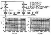
도 6은 LED(발광 다이오드: light emitting diode)들을 제어하기 위한 두 직렬 공진 LC 회로(two series resonant LC circuit)의 주파수 도메인 시뮬레이션의 결과를 도시한 도면;
도 7은 LED 구동 회로의 시간 도메인 시뮬레이션의 결과를 도시한 도면.1 is a diagram of a physical layer management system for use in an interconnection arrangement in accordance with an embodiment of the present invention;
2 is a block diagram illustrating one embodiment of the present invention for use in a cross-connect arrangement;
Figure 3a is a schematic view of a patch cord connection according to one embodiment of the present invention;
Figure 3B is a block diagram illustrating connection tracking hardware in accordance with an embodiment of the present invention;
3C is a side view of a patch panel and plug hardware according to an embodiment of the invention;
4 is a schematic diagram of a patch cord according to an embodiment of the present invention;
5 is a schematic diagram of a patch cord according to another embodiment of the present invention;
Figure 6 shows the results of frequency domain simulation of two series resonant LC circuits for controlling LEDs (light emitting diodes);
7 is a diagram showing a result of a time domain simulation of an LED driving circuit;
상기 시스템을 포함하는 구성요소들을 사용자에 대해서 가능한 한 간단하고 방해되지 않게 하는 것이 물리 계층 관리 장비의 개발에 있어서 유리하다. 사용자가 패치 코드 이동, 추가 혹은 변경 등과 같은 간단한 과업을 수행하는데 새롭고 복잡한 절차를 적용할 필요가 있다면, 물리 계층 관리 시스템의 성공 확률이 저감된다. RFID 기술은 몇몇 PLM 시스템에 의해 요구되는 갈바닉 접속들을 제거함으로써 해당 시스템의 신뢰성을 증가시킬 뿐만 아니라 MAC 절차의 복잡성을 감소시키도록 제공된다.It is advantageous in the development of physical layer management equipment to make the components including the system as simple and unobtrusive as possible for the user. If the user needs to apply new and complex procedures to perform simple tasks such as patch code movement, addition or change, the probability of success of the physical layer management system is reduced. RFID technology is provided to reduce the complexity of MAC procedures as well as to increase the reliability of the system by eliminating the galvanic connections required by some PLM systems.
패치 코드 MAC 절차는 일반적으로, 적어도 하나의 패치 패널을 포함하는 패치 필드라 불리는 네트워크의 영역 내에서 수행된다. 일반적으로, 패치 패널을 네트워크에 통합하는 접근법에는 2가지, 즉 상호접속과 교차-접속이 있다. 상호접속 배치형태에서는, 도 1에 도시된 바와 같이, 단일의 패치 패널이 일반적으로 네트워크의 수평 케이블링과 다른 네트워크 요소, 예컨대, 스위치 사이에 배치된다. 상호접속 배치형태에 있어서, 패치 필드는 패치 패널과 스위치 사이에 있다. 이에 대해서, 교차-접속 배치형태는, 도 2에 도시된 바와 같이, 상기 수평 케이블링과 스위치 사이에 있는 2개의 패치 패널을 이용한다. 교차-접속 배치형태에 있어서의 패치 필드는 두 패치 패널 사이에 위치된다. 상호접속 혹은 교차-접속 배치형태에서 사용하기 위하여 적응될 수 있는 PLM 시스템을 설계하는 것이 유리하다.The patch code MAC procedure is generally performed in the area of the network called the patch field, which includes at least one patch panel. In general, there are two approaches to integrating patch panels into the network: interconnection and cross-connection. In the interconnection arrangement, a single patch panel is typically placed between the horizontal cabling of the network and other network elements, e.g. switches, as shown in Fig. In the interconnection configuration, the patch field is between the patch panel and the switch. In contrast, the cross-connect arrangement uses two patch panels between the horizontal cabling and the switch, as shown in Fig. The patch field in the form of a cross-connect arrangement is located between the two patch panels. It is advantageous to design a PLM system that can be adapted for use in interconnection or cross-connect deployment configurations.
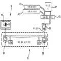
도 1의 도면 (A)는 상호접속 배치 형태에서 물리 계층 관리 시스템(10)의 패치 필드 부분을 도시한 것으로, 여기서 패치 패널(22)은 수평 케이블링(11)과 이더넷 스위치(14) 사이에 위치되어 있다. 이더넷 스위치(14)(또는 등가의 관리된 장비) 내의 RJ45 잭(12)에는, RFID 태그(16)가 설치되어 있고, 이 태그는 RFID 판독기 시스템(reader system)을 개재해서 판독될 수 있는 내장된 RFID ID 칩 및 안테나를 포함한다. 스위치 내의 잭(12)과 패치 패널(22) 내의 잭(20) 사이에 접속을 제공하기 위한 패치 코드(18)는 코드(32)의 양 단부 상에 있는 플러그(28, 30)에 설치된 안테나(24, 26)를 구비한다. 패치 코드(18)는 이더넷 스위치(14) 내의 RFID 태그(16)와 패치 패널(22) 내의 판독기(34) 사이에 통신을 허용한다. RFID 판독기(34)는 패치 코드(18)가 접속되는 패치 패널의 잭에 설치된 안테나(36)를 개재해서 안테나(26)와 통신한다.1 shows a patch field portion of a physical
패치 코드(18) 내의 두 안테나(24, 26)는 코드(32) 내의 제5번째 와이어 쌍(38)을 통해서 서로 접속된다. 제5번째 와이어 쌍을 이용하는 것은 "대역외"(out of band) 통신 기술이라 불리는데, 이는 이더넷 신호에 통상 이용되는 "대역내"(in-band) 와이어 쌍들의 어느 것도 이용하지 않기 때문이다. 이와 같이 해서, 패치 패널(22) 내의 RFID 판독기(34)는 이더넷 스위치 포트들 내에 있는 잭(12)들에 내장된 RFID 태그(16)와 통신할 수 있다. PLM 정보의 통신을 위하여 제5번째 와이어 쌍(38)을 이용하는 것은 구리 네트워크(copper network)에서 이더넷 신호를 포함하는 나머지 4개의 와이어 쌍의 성능 무결성(performance integrity)을 확실하게 한다. 이 5개의 와이어 쌍 케이블 배치형태 전략은 비차폐 연선 쌍(unshielded twisted pair: UTP) 및 차폐 연선 쌍(shielded twisted pair: STP) 케이블링 시스템과 협력할 것이다.The two
바람직하게는, 이 방식에 이용되는 안테나는 전자파의 이용에 의해 통신하지 않고 오히려 근접장 결합 통신의 유형을 이용해서 수신 안테나와 통신한다.Preferably, the antenna used in this manner does not communicate by the use of electromagnetic waves, but instead communicates with the receive antenna using a type of near field coupling communication.
각 스위치 포트와 연관된 RFID 태그(16)가 포함할 수 있는 정보의 유형으로는, RFID 번호, 스위치 포트 번호, 스위치 번호, 스위치 유형, 랙 번호(rack number), 물리적 위치 설명, 제공 시간(패치 패널과 스위치 포트 사이의 패치 접속이 완성된 시간을 반영함) 등을 들 수 있다. 패치 패널(22)이 패치 패널의 포트들이 접속되는 이더넷 포트들에 구비된 RFDD 태그(16)들과 통신할 경우, 해당 패널은 패치 필드를 완전하게 문서화하기 위한 필요한 정보를 지닐 것이다. 패치 필드에 관한 정보는 관리 접속부를 통해서 네트워크 관리 시스템에 전송될 수 있다.The types of information that the
고밀도 스위치 장비(예컨대, 48-포트 1-랙-유닛 스위치)를 지원하기 위하여, RFID 태그들이 이웃하는 RJ45 잭(12)들 사이에서 누설을 수직 및 수평 양쪽 모두에서 최소화하도록 하는 방식으로 장착되어야만 한다. 잭들과 플러그들 상의 제안된 태크 위치들은 각각 도 1(B) 및 도 1(C)에 도시되어 있다. 본 발명의 실시형태는 이더넷 포트들 내에 RFID 태그(16)들이 설치된 것을 도시하고 있지만, 이더넷 포트들과 연관된 RFID 태그들은 대안적으로 포트들의 외부, 예를 들어, 이더넷 스위치(14)의 면판(faceplate) 상에 설치될 수도 있다.In order to support high density switch equipment (e.g., a 48-port 1-rack-unit switch), the RFID tags must be mounted in a manner that minimizes leakage both vertically and horizontally between neighboring
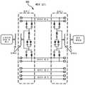
도 2는 교차-접속 배치형태에서 이용하기 위한 본 발명에 따른 PLM 시스템(39)의 평면도를 도시하고 있다. 이 배치형태에 있어서, 2개의 패치 패널(40, 42)이 수평 케이블링(44)과 이더넷 스위치(46) 사이에 설치되고, 패치 필드는 두 패치 패널(40, 42) 사이에 위치되어 있다. 이더넷 케이블(47)은 이더넷 스위치를 패치 패널(40)에 접속한다. 도 2에서는, 도 1에서와 마찬가지로, 이더넷 스위치(46)로부터 수평 케이블링(44)까지의 단지 하나의 링크가 도시되어 있지만, 본 발명에 따른 시스템들은 네트워크 하드웨어의 부분들 간에 다수의 링크를 지니는 네트워크 환경에 적용되는 것임을 이해할 필요가 있다. 이 실시형태에서, 패치 패널(40, 42)에 구비된 RFID 판독기(34a, 34b)는 서로 통신하여, 해당 패치 패널(40, 42)의 포트들 사이에 접속된 패치 코드(18)들의 물리적 접속성을 분석한다. 패치 패널(40, 42)의 포트들과 연관된 안테나(36a, 36b)는 패치 코드(18)들 내에 구비된 제5번째 와이어 쌍(38)을 개재해서 서로 통신한다. 안테나(36a, 36b)는 각각 패치 코드(18)의 플러그들 내의 안테나(24, 26)에 대해서 전송된 신호를 통해서 통신한다.Figure 2 shows a top view of a PLM system 39 in accordance with the present invention for use in a cross-connect configuration. In this configuration, two patch panels 40 and 42 are installed between the horizontal cabling 44 and the Ethernet switch 46, and the patch field is located between the two patch panels 40 and 42. The Ethernet cable 47 connects the Ethernet switch to the patch panel 40. 2, only one link from the Ethernet switch 46 to the horizontal cabling 44 is shown, but the systems according to the present invention are not limited to having a plurality of links between portions of the network hardware It is necessary to understand that the present invention is applied to a network environment. In this embodiment, the RFID readers 34a and 34b provided in the patch panels 40 and 42 communicate with each other to detect the physical connection of the
도 3a의 도면 (i)은 패치 코드(18)의 구성요소들을 더욱 상세히 도시한 개략도이다. 패치 코드의 플러그들 내로 발광 다이오드들(LEDs)을 내장시켜 MAC을 이용가능하게 하는 것이 바람직하다. 도 3a(i)의 실시형태에서, LED(48a, 48b 및 50a, 50b)는 패치 코드(18)의 플러그(28, 30) 내에 구비되어 있다. 바람직하게는, LED(48a, 50a)는 적색이고, LED(48b, 50b)는 녹색이다. 이들 LED는, 제9번째 와이어와 제10번째 와이어 상에 배치된 통신 신호가 각 LED와 연관된 공진 주파수에서 작동할 때 개별적으로 혹은 동시에 발광될 수 있다. 일 실시형태에서, 패치 코드의 각 단부 상의 두 플러그의 LED는 특정 신호에 응답하여 발광할 것인데, 그 이유는 LED들이 병렬 상태인 것이 효과적이기 때문이다. 이 실시형태에서, 패치 코드는 대칭 상태이다.Figure (a) of Figure 3a is a schematic diagram showing the components of the
두 세트의 LED(48a, 48b 및 50a, 50b)는 작동 하에 있는 LED들의 다수의 공진 주파수를 제공함으로써 독립적으로 작동하게 되어 있을 수 있다. 예를 들어, 패치 코드(18)의 제1플러그(28) 내의 LED(48a, 48b)는 주파수(F1, F2)에서 발광할 수 있고, 패치 코드(18)의 제2플러그(30) 내의 LED(50a, 50b)는 주파수(F3, F4)에서 발광할 수 있으며, 따라서, 4개의 독립적인 주파수가 개별적으로 혹은 그룹으로 LED들의 발광을 제어하는데 이용될 수 있다. LED들에 대한 상이한 공명 주파수에 응답하도록 설정하는 것은, 커패시터(52a, 52b, 54a, 54b) 및/또는 인덕터(56, 58)의 값들을 변화시킴으로써 달성될 수 있다. 적절한 LED 주파수는 80㎑ 및 3㎒(도 6에 도시됨)와 같은 값들을 포함하지만, 900㎒의 RFID 주파수는 표준 구성요소의 채용을 허용한다. 도 3a(ii)는 두 LED(48a, 48b)에 대한 상이한 신호 주파수의 할당을 도시하고 있다.The two sets of
도 3a의 실시형태는, 구리 통신 네트워크와 관련하여 설명되었지만, 섬유 네트워크에 이용하기 위하여 구성될 수도 있다.Although the embodiment of FIG. 3A has been described in connection with a copper communication network, it may be configured for use in a fiber network.
도 3b는 본 발명의 일 실시형태에 따른 패치 코드들을 트래킹하는데 이용되는 하드웨어를 보다 상세히 도시한 블록도이다. 패치 코드(18)는 플러그들을 표시하지 않은 간략화된 도면에 도시되어 있다. 안테나(24, 26)는 코일 안테나로서 도시되어 있다. 패치 코드(18)의 패치 패널 측 상에서, 안테나(26)는 패치 코드가 접속된 패치 패널 포트와 연관된 안테나(36)에 자기적으로 결합한다. 도 1(A)에 도시된 바와 같은 RFID 판독기(34)를 포함하는 패치 패널 내의 하드웨어는 판독기 집적회로(IC)(37), 및 패치 코드(18)의 플러그들 내에서 예를 들어 적색 및 녹색 LED와 연관된 주파수를 생성하는 신호 생성기(41, 43)를 포함한다. 판독기 IC(37) 및 신호 생성기(41, 43)는 멀티플렉서(multiplexor: MUX) 혹은 선택기(45)에 접속되어, 요청된 신호를 안테나(36)에 제공한다. 해당 신호는 이어서 안테나(24)로 패치 코드(18)의 길이 아래쪽으로 전송된다. 상기 신호는, 안테나(24)로부터, 패치 코드(18)가 플러그되어 있는 스위치 포트와 연관된 RFID 태그(16)로 연결된다. RFID 태그(16)는 안테나(17) 및 RFID IC(19)를 포함한다. 안테나(24)에 자기적으로 결합된 안테나(17)는, RFID IC(19)로부터 안테나(24)로 정보를 전송한다. 해당 정보 신호는 이어서 안테나(26, 36)를 통해서 판독기 IC(37)로 패치 코드(18)의 길이를 주행한다. 그 지점에서, 판독기 IC(37)는 패치 패널 포트와 스위치 포트 간의 접속에 대한 필요한 정보를 수신한다.3B is a block diagram illustrating in more detail the hardware used to track patch codes in accordance with an embodiment of the invention. The
본 발명의 몇몇 실시형태에 따른 패치 패널들에 이용하기 위한 RFID 판독기들은 당해 산업에서 공지되고 텍사스 인스트루먼트사 및 필립스사 등과 같은 회사에서 제작된 RFID 판독기일 수 있다. 예를 들어 스위치 포트들 내에서, 본 발명의 실시형태와 함께 이용하기 위한 RFID 태그들은 당해 산업에서 공지되고 임핀지(Impinj), 인벤고(Invengo) 및 비오데(Biode) 등과 같은 회사에서 제작된 RFID 태그들을 포함한다. 본 발명의 실시형태들에서 이용하기 위한 RFID 판독기들은 다수의 상이한 주파수(예컨대, 900㎒, 13㎒, 125㎑, 혹은 기타 RFID 주파수)에서 작동할 수 있다.RFID readers for use in patch panels according to some embodiments of the present invention may be RFID readers manufactured in companies such as Texas Instruments and Philips, which are well known in the art. For example, within switch ports, RFID tags for use with embodiments of the present invention may be used in a variety of applications, such as those known in the industry and manufactured by companies such as Impinj, Invengo and Biode, RFID tags. RFID readers for use in embodiments of the present invention may operate at a number of different frequencies (e.g., 900 MHz, 13 MHz, 125 kHz, or other RFID frequency).
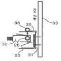
도 3c는 본 발명의 일 실시형태에서 이용되는 통신 하드웨어의 추가적인 상세를 도시하고 있다. 패치 패널의 잭(20)은 패치 코드(18)의 플러그(30)를 수용한다. 플러그(30)의 안테나(26)는 잭(20)과 연관된 안테나(36)에서와 마찬가지로 코일 안테나로서 도시되어 있다. 안테나(36)는 안테나 접속부(35)를 개재해서 패치 패널의 인쇄회로기판(33)에 접속된다. 이 접속은 독립적으로 이루어질 수 있거나 잭(20)와 연관된 인쇄회로기판(31)을 개재해서 이루어질 수 있다. 도 3b에 도시된 RFID 판독기 IC(37)는 바람직하게는 패치 패널 PCB(33) 상에 위치되어 있다. 도 3c에 도시된 안테나들은 보여주기 위하여 도면에서 각도가 맞추어져 있다. 바람직한 실시형태에서는, 이들은 공통 중심선을 따라 서로 대항할 것이다.3C shows additional details of the communication hardware used in an embodiment of the present invention. The
도 4 및 도 5는 구리-기반 이더넷 시스템 내의 4개의 표준 와이어 쌍을 통하여 공통-모드 신호를 이용해서 RFID 판독기들과 RFID 태그들 간에 통신을 제공할 뿐만 아니라, LED들을 발광하기 위한 신호를 제공하는 패치 코드(60, 62)의 대안적인 실시형태들을 도시하고 있다. 도 4의 패치 코드(60)에 있어서, 두 와이어 쌍은, 표준 이더넷 통신 신호에 부가해서, RFID 신호들과 LED 발광 신호들 양쪽 모두를 전송하는데 이용된다. 도 5의 패치 코드(62)에 있어서, 두 와이어 쌍은 RFID 신호들을 전송하는데 이용되고, 나머지 두 쌍이 LED 발광 신호들을 전송하는데 이용된다. 도 5의 실시형태에 있어서, LED 신호 접속부(도시생략)는 패치 코드(62)의 쌍 C, D와 연관된 접촉부들과 패치 패널에서의 포트 접촉부들 사이에 설치되므로, 패치 패널은 패치 코드(62)의 플러그들에 구비된 LED(48a, 48b 및 50a, 50b)를 발광하기 위하여 신호들과 전력을 제공할 수 있다.Figures 4 and 5 illustrate the use of common-mode signals over four standard wire pairs in a copper-based Ethernet system to provide communication between RFID readers and RFID tags, as well as to provide signals for emitting LEDs Alternative embodiments of
도 6 및 도 7은 각각의 구동 회로를 구비한 직렬 공진 LC 회로들의 시뮬레이션의 결과를 도시하고 있다. 도 6은 두 직렬 공진 LC 회로의 주파수-도메인 시뮬레이션의 결과를 도시하고 있다. 이 시뮬레이션은, 두 LED가 상이한 주파수에서 제어 신호를 제공함으로써 독립적으로 제어될 수 있는 것을 나타낸다. 도 7은 LED를 구동하는데 이용하기 위한 두 공진 회로의 시간-도메인 시뮬레이션의 결과를 도시하고, 또한 LED가 적절하게 독립적으로 제어될 수 있는 것을 나타내고 있다.Figures 6 and 7 show the results of a simulation of series resonant LC circuits with respective drive circuits. Figure 6 shows the results of a frequency-domain simulation of two series resonant LC circuits. This simulation shows that the two LEDs can be independently controlled by providing control signals at different frequencies. Figure 7 shows the results of a time-domain simulation of two resonant circuits for use in driving LEDs, and also shows that the LEDs can be controlled independently and appropriately.
Claims (18)
Translated fromKorean연관된 RFID 판독기(reader)를 구비한 제2잭; 및
두 개의 플러그를 구비한 패치 코드(patch cord)를 포함하되,
각 플러그는 플러그 안테나와 발광 다이오드(LED) 회로를 구비하고, 각 LED 회로는 제1LED를 포함하고 제1공진 주파수를 지니는 제1회로와, 제2LED를 포함하고 제2공진 주파수를 지니는 제2회로를 구비하며, 상기 제1공진 주파수는 상기 제2공진 주파수와는 상이하고,
각 LED 회로는 서로 전기적으로 접속되며, 각 플러그 안테나는 서로 전기적으로 접속되고, 상기 신호 생성기는 상기 제1공진 주파수와 상기 제2공진 주파수 중 적어도 하나의 주파수에서 신호를 생성하도록 구성되어, 해당 신호의 생성은 상기 제1LED와 상기 제2LED 중 적어도 하나를 발광시키고, 상기 RFID 태그는 상기 패치 코드를 통하여 상기 RFID 판독기에 신호를 전송하도록 구성된 것을 특징으로 하는 물리 계층 관리 시스템.
A first jack having an associated RFID tag and an associated signal generator;
A second jack having an associated RFID reader; And
And a patch cord having two plugs,
Each plug comprising a plug antenna and a light emitting diode (LED) circuit, wherein each LED circuit comprises a first circuit comprising a first LED and having a first resonant frequency, a second circuit comprising a second LED and having a second resonant frequency, Wherein the first resonance frequency is different from the second resonance frequency,
Wherein each LED circuit is electrically connected to each other and each plug antenna is electrically connected to each other and the signal generator is configured to generate a signal at at least one of the first resonance frequency and the second resonance frequency, Is configured to emit at least one of the first LED and the second LED, and the RFID tag is configured to transmit a signal to the RFID reader through the patch cord.
2. The method of claim 1, wherein the first circuit comprises a first capacitor and the second circuit comprises a second capacitor, wherein the first capacitor has a different capacitance than the second capacitor. Hierarchical management system.
3. The physical layer management system of claim 2, wherein the first circuit is in parallel with the second circuit, and the first and second circuits are also in series with an inductor.
The system of claim 1, wherein the RFID tag is configured to transmit a signal to an RFID reader via an out-of-band wire pair through the patch code.
5. The RFID tag of claim 4, wherein the RFID tag is configured to electrically connect the plug antenna to each other via the out-of-band wire pair, thereby transmitting a signal to the RFID reader through the out-of-band wire pair via the patch cord Physical layer management system.
6. The system of claim 5, wherein the LED circuits are electrically connected to each other via the out-of-band wire pair.
The system of claim 1, wherein the RFID tag is configured to transmit signals to the RFID reader in a common mode signal through two pairs of wires of the patch cord.
8. The RFID tag of claim 7, wherein the RFID tag is configured to transmit signals to the RFID reader in a common mode signal through the two wire pairs by electrically connecting the plug antennas to each other via two pairs of wires of the patch cord Physical layer management system.
9. The physical layer management system of claim 8, wherein the LED circuits are connected to each other through the same pair of wires connecting the plug antennas.
9. The physical layer management system according to claim 8, wherein the LED circuits are connected to each other via two wire pairs different from those connecting the plug antennas.
The system of claim 1, wherein the first LED is red and the second LED is green.
2. The physical layer management system according to claim 1, wherein the first resonance frequency is approximately 80 kHz and the second resonance frequency is approximately 3 MHz.
The method of claim 1, wherein the signal transmitted from the RFID tag to the RFID reader via the patch code includes at least one of an RFID number, a switch port number, a switch type, a rack number, a physical location description, And a physical layer management system for managing physical layer management information.
제1단부, 제2단부, 및 상기 제1단부와 상기 제2단부 사이로 뻗은 복수의 신호 쌍(pair)을 포함하는 통신 케이블;
상기 제1단부에 연결된 제1플러그 및 상기 제2단부에 연결된 제2플러그를 포함하고,
상기 플러그 중 적어도 하나는 플러그 안테나 및 적어도 하나의 LED 회로를 가지고,
각각의 LED 회로는 적어도 하나의 발광 다이오드(LED)를 포함하고 적어도 하나의 공진 주파수를 지니는 적어도 하나의 회로를 포함하는 것을 특징으로 하는 물리 계층 관리 시스템용 패치 코드.A patch code for a physical layer management system,
A communication cable comprising a first end, a second end, and a plurality of signal pairs extending between the first end and the second end;
A first plug connected to the first end and a second plug connected to the second end,
At least one of said plugs having a plug antenna and at least one LED circuit,
Wherein each LED circuit comprises at least one circuit comprising at least one light emitting diode (LED) and having at least one resonant frequency.
15. The method of claim 14 wherein the at least one LED circuit comprises a first circuit having a first LED and a first resonant frequency and a second circuit having a second LED and a second resonant frequency, A patch code for a physical layer management system.
The patch code according to claim 15, wherein the first resonance frequency is different from the second resonance frequency.
15. The method of claim 14, wherein the plurality of signal pairs comprises a plurality of pairs of Ethernet signals having a first pair of Ethernet signals and a second pair of Ethernet signals, 2 < / RTI > Ethernet signal pair.
Applications Claiming Priority (3)
| Application Number | Priority Date | Filing Date | Title |
|---|---|---|---|
| US25480009P | 2009-10-26 | 2009-10-26 | |
| US61/254,800 | 2009-10-26 | ||
| PCT/US2010/054038WO2011056541A1 (en) | 2009-10-26 | 2010-10-26 | Physical layer management using rfid and near-field coupling techniques |
Publications (2)
| Publication Number | Publication Date |
|---|---|
| KR20120091230A KR20120091230A (en) | 2012-08-17 |
| KR101471128B1true KR101471128B1 (en) | 2014-12-09 |
Family
ID=43530812
Family Applications (1)
| Application Number | Title | Priority Date | Filing Date |
|---|---|---|---|
| KR1020127013059AExpired - Fee RelatedKR101471128B1 (en) | 2009-10-26 | 2010-10-26 | Physical layer management using rfid and near-field coupling techniques |
Country Status (5)
| Country | Link |
|---|---|
| US (2) | US8427335B2 (en) |
| EP (2) | EP2494789B1 (en) |
| JP (1) | JP5443608B2 (en) |
| KR (1) | KR101471128B1 (en) |
| WO (1) | WO2011056541A1 (en) |
Families Citing this family (24)
| Publication number | Priority date | Publication date | Assignee | Title |
|---|---|---|---|---|
| KR101471128B1 (en)* | 2009-10-26 | 2014-12-09 | 팬듀트 코포레이션 | Physical layer management using rfid and near-field coupling techniques |
| WO2012027345A2 (en) | 2010-08-23 | 2012-03-01 | Commscope, Inc. Of North Carolina | Conductive elements in cable jackets and separators |
| US8947106B2 (en) | 2011-01-21 | 2015-02-03 | Commscope, Inc. Of North Carolina | Plug insertion detection circuits that sense a change in capacitance and related methods and communications connectors |
| US20130078848A1 (en)* | 2011-09-23 | 2013-03-28 | Andrew Llc | Intelligent Patching Systems and Methods Using Radio Frequency Identification Tags that are Interrogated Over Network Cabling and Related Communications Connectors |
| US9590761B2 (en) | 2011-09-23 | 2017-03-07 | Commscope Technologies Llc | Detective passive RF components using radio frequency identification tags |
| US20130181816A1 (en)* | 2012-01-17 | 2013-07-18 | International Business Machines Corporation | Mechanism and method for rfid cable path labeling, identification, and inventory |
| US9678133B2 (en) | 2012-03-12 | 2017-06-13 | Commscope, Inc. Of North Carolina | Intelligent patching systems and methods using electrical cable diagnostic tests and inference-based mapping techniques |
| EP3428806B1 (en)* | 2012-07-11 | 2021-11-03 | CommScope Connectivity UK Limited | Heterogeneous and/or hosted physical layer management system and method |
| US9059590B2 (en)* | 2013-02-26 | 2015-06-16 | Bby Solutions, Inc. | Universal battery charger system and method |
| US9225127B2 (en)* | 2013-03-20 | 2015-12-29 | Lenovo (Singapore) Pte. Ltd. | Connection illumination using communication elements |
| US11212177B2 (en)* | 2013-08-01 | 2021-12-28 | Commscope Connectivity Uk Limited | Hosted physical layer management or automated infrastructure management system having software only configuration and/or local hardware appliance |
| WO2015023768A1 (en)* | 2013-08-14 | 2015-02-19 | Adc Telecommunications, Inc. | Inferring physical layer connection status of generic cables from planned single-end connection events |
| US9500814B2 (en)* | 2014-03-26 | 2016-11-22 | Commscope Technologies Llc | Optical adapter module with managed connectivity |
| CN105720430B (en)* | 2014-12-01 | 2018-04-10 | 3M创新有限公司 | Patch and grafting wire management system and management method |
| US9569940B2 (en)* | 2015-05-28 | 2017-02-14 | Lenovo Enterprise Solutions (Singapore) Pte. Ltd. | Identification of ports from which cables have been recently removed and that have the same physical form factor using existing visual port indicators |
| WO2017062231A1 (en)* | 2015-10-08 | 2017-04-13 | Commscope Technologies Llc | Communication media and methods for providing indication of signal power to a network entity |
| BR102017021868A2 (en) | 2017-10-10 | 2019-05-07 | Furukawa Electric Latam S.A. | IDENTIFICATION SYSTEM OF DOOR PAIRS AND THEIR CONNECTION CABLES IN TELECOMMUNICATION NETWORK PANELS |
| CN107748854A (en)* | 2017-10-27 | 2018-03-02 | 广东康利达物联科技股份有限公司 | A kind of POE powers integrated RFID reader and its communication means |
| US10938167B2 (en) | 2018-03-06 | 2021-03-02 | Commscope Technologies Llc | Automated capture of information about fixed cabling |
| CN114402626A (en) | 2019-09-12 | 2022-04-26 | 康普技术有限责任公司 | Internet of Things (IOT) systems for cabling infrastructure |
| MX2022012892A (en) | 2020-04-22 | 2023-01-16 | Furukawa Electric Latam S A | Identification device for connection cables in telecommunication-network jumper boards. |
| US11522319B2 (en)* | 2020-06-08 | 2022-12-06 | Global Inventive Consulting Inc. | RFID-enabled electrical connector |
| US11256888B2 (en)* | 2020-06-08 | 2022-02-22 | Global Inventive Consulting, Inc. | System and method employing wireless high-voltage interlocking loop using RFID-enabled electrical connectors containing conductive material |
| WO2022081751A1 (en)* | 2020-10-16 | 2022-04-21 | Commscope Technologies Llc | Port occupancy detection |
Citations (4)
| Publication number | Priority date | Publication date | Assignee | Title |
|---|---|---|---|---|
| US6784802B1 (en)* | 1999-11-04 | 2004-08-31 | Nordx/Cdt, Inc. | Real time monitoring of cable patch panel |
| WO2006063023A1 (en)* | 2004-12-06 | 2006-06-15 | Commscope Solutions Properties, Llc | Telecommunications patching system that utilizes rfid tags to detect and identify patch cord interconnections |
| US20080122579A1 (en)* | 2006-11-29 | 2008-05-29 | Commscope Solutions Properties, Llc | Telecommunications patching system that facilitates detection and identification of patch cords |
| US20090096581A1 (en)* | 2007-10-12 | 2009-04-16 | Commscope, Inc. Of North Carolina | Communications Patching Systems with Radio Frequency Identification Antenna Switching Circuits |
Family Cites Families (13)
| Publication number | Priority date | Publication date | Assignee | Title |
|---|---|---|---|---|
| JP2004226512A (en)* | 2003-01-21 | 2004-08-12 | Tokyo Tsushinki Kogyo Kk | Optical fiber connector connection parts |
| JP2005092107A (en)* | 2003-09-19 | 2005-04-07 | Tokyo Tsushinki Kogyo Kk | Management system of transmission component using connector plug with memory |
| JP2006054118A (en)* | 2004-08-12 | 2006-02-23 | Tokyo Tsushinki Kogyo Kk | Wiring support system |
| US7443915B2 (en)* | 2004-11-30 | 2008-10-28 | Tyco Electronics Corporation | Method and apparatus for providing out of band communications over structured cabling |
| JP2007158993A (en)* | 2005-12-08 | 2007-06-21 | Tokyo Tsushinki Kogyo Kk | Wiring management system |
| JP2007189774A (en)* | 2006-01-11 | 2007-07-26 | Tokyo Tsushinki Kogyo Kk | Wiring management system |
| US20070248358A1 (en)* | 2006-04-19 | 2007-10-25 | Michael Sauer | Electrical-optical cable for wireless systems |
| GB0608456D0 (en)* | 2006-04-28 | 2006-06-07 | Tyco Electronics Amp Espana | An assembly for permitting power-over-ethernet connection |
| US7965186B2 (en)* | 2007-03-09 | 2011-06-21 | Corning Cable Systems, Llc | Passive RFID elements having visual indicators |
| WO2009072929A1 (en)* | 2007-12-06 | 2009-06-11 | Yulia Alekseevna Yashukova | System for monitoring the detachable joint of a cable path using radio frequency identifications |
| DE102009013034B4 (en)* | 2009-03-16 | 2015-11-19 | Olympus Winter & Ibe Gmbh | Autoclavable charging device for an energy store of a surgical instrument and method for charging a rechargeable energy store in an autoclaved surgical instrument or for an autoclaved surgical instrument |
| CN102598705B (en)* | 2009-06-29 | 2015-06-17 | 北卡罗来纳科姆斯科普公司 | Patch panel, patch panel system and method of displaying patch cord connection information |
| KR101471128B1 (en)* | 2009-10-26 | 2014-12-09 | 팬듀트 코포레이션 | Physical layer management using rfid and near-field coupling techniques |
- 2010
- 2010-10-26KRKR1020127013059Apatent/KR101471128B1/ennot_activeExpired - Fee Related
- 2010-10-26JPJP2012535452Apatent/JP5443608B2/ennot_activeExpired - Fee Related
- 2010-10-26USUS12/911,796patent/US8427335B2/ennot_activeExpired - Fee Related
- 2010-10-26EPEP10775999.5Apatent/EP2494789B1/ennot_activeNot-in-force
- 2010-10-26WOPCT/US2010/054038patent/WO2011056541A1/enactiveApplication Filing
- 2010-10-26EPEP18179110.4Apatent/EP3396971B1/enactiveActive
- 2013
- 2013-04-16USUS13/864,001patent/US8665107B2/ennot_activeExpired - Fee Related
Patent Citations (4)
| Publication number | Priority date | Publication date | Assignee | Title |
|---|---|---|---|---|
| US6784802B1 (en)* | 1999-11-04 | 2004-08-31 | Nordx/Cdt, Inc. | Real time monitoring of cable patch panel |
| WO2006063023A1 (en)* | 2004-12-06 | 2006-06-15 | Commscope Solutions Properties, Llc | Telecommunications patching system that utilizes rfid tags to detect and identify patch cord interconnections |
| US20080122579A1 (en)* | 2006-11-29 | 2008-05-29 | Commscope Solutions Properties, Llc | Telecommunications patching system that facilitates detection and identification of patch cords |
| US20090096581A1 (en)* | 2007-10-12 | 2009-04-16 | Commscope, Inc. Of North Carolina | Communications Patching Systems with Radio Frequency Identification Antenna Switching Circuits |
Also Published As
| Publication number | Publication date |
|---|---|
| EP3396971B1 (en) | 2019-12-04 |
| EP3396971A1 (en) | 2018-10-31 |
| WO2011056541A1 (en) | 2011-05-12 |
| US8665107B2 (en) | 2014-03-04 |
| US8427335B2 (en) | 2013-04-23 |
| US20110097925A1 (en) | 2011-04-28 |
| JP5443608B2 (en) | 2014-03-19 |
| EP2494789B1 (en) | 2018-06-27 |
| US20130260603A1 (en) | 2013-10-03 |
| KR20120091230A (en) | 2012-08-17 |
| JP2013509110A (en) | 2013-03-07 |
| EP2494789A1 (en) | 2012-09-05 |
Similar Documents
| Publication | Publication Date | Title |
|---|---|---|
| KR101471128B1 (en) | Physical layer management using rfid and near-field coupling techniques | |
| US10505663B2 (en) | Detecting passive RF components using radio frequency identification tags | |
| US9113236B2 (en) | Physical layer management using RFID modules and common mode signaling | |
| US8461964B2 (en) | Communications patching systems with radio frequency identification antenna switching circuits | |
| US20130078848A1 (en) | Intelligent Patching Systems and Methods Using Radio Frequency Identification Tags that are Interrogated Over Network Cabling and Related Communications Connectors | |
| US8649651B2 (en) | Patch panel cable information detection systems and methods | |
| US9196999B2 (en) | Two-part modular connector and smart managed interconnect link using the two-part modular connector | |
| US8686870B2 (en) | Physical layer management for interconnect configurations using RFID chip technology | |
| GB2464204A (en) | RFID Providing Device Orientation Data | |
| EP2891288B1 (en) | Detecting passive rf components using radio frequency identification tags |
Legal Events
| Date | Code | Title | Description |
|---|---|---|---|
| PA0105 | International application | St.27 status event code:A-0-1-A10-A15-nap-PA0105 | |
| PG1501 | Laying open of application | St.27 status event code:A-1-1-Q10-Q12-nap-PG1501 | |
| A201 | Request for examination | ||
| A302 | Request for accelerated examination | ||
| P11-X000 | Amendment of application requested | St.27 status event code:A-2-2-P10-P11-nap-X000 | |
| P13-X000 | Application amended | St.27 status event code:A-2-2-P10-P13-nap-X000 | |
| PA0201 | Request for examination | St.27 status event code:A-1-2-D10-D11-exm-PA0201 | |
| PA0302 | Request for accelerated examination | St.27 status event code:A-1-2-D10-D17-exm-PA0302 St.27 status event code:A-1-2-D10-D16-exm-PA0302 | |
| E701 | Decision to grant or registration of patent right | ||
| PE0701 | Decision of registration | St.27 status event code:A-1-2-D10-D22-exm-PE0701 | |
| GRNT | Written decision to grant | ||
| PR0701 | Registration of establishment | St.27 status event code:A-2-4-F10-F11-exm-PR0701 | |
| PR1002 | Payment of registration fee | St.27 status event code:A-2-2-U10-U12-oth-PR1002 Fee payment year number:1 | |
| PG1601 | Publication of registration | St.27 status event code:A-4-4-Q10-Q13-nap-PG1601 | |
| FPAY | Annual fee payment | Payment date:20171124 Year of fee payment:4 | |
| PR1001 | Payment of annual fee | St.27 status event code:A-4-4-U10-U11-oth-PR1001 Fee payment year number:4 | |
| FPAY | Annual fee payment | Payment date:20181219 Year of fee payment:5 | |
| PR1001 | Payment of annual fee | St.27 status event code:A-4-4-U10-U11-oth-PR1001 Fee payment year number:5 | |
| FPAY | Annual fee payment | Payment date:20191126 Year of fee payment:6 | |
| PR1001 | Payment of annual fee | St.27 status event code:A-4-4-U10-U11-oth-PR1001 Fee payment year number:6 | |
| PR1001 | Payment of annual fee | St.27 status event code:A-4-4-U10-U11-oth-PR1001 Fee payment year number:7 | |
| PC1903 | Unpaid annual fee | St.27 status event code:A-4-4-U10-U13-oth-PC1903 Not in force date:20211204 Payment event data comment text:Termination Category : DEFAULT_OF_REGISTRATION_FEE | |
| PC1903 | Unpaid annual fee | St.27 status event code:N-4-6-H10-H13-oth-PC1903 Ip right cessation event data comment text:Termination Category : DEFAULT_OF_REGISTRATION_FEE Not in force date:20211204 |