KR101469934B1 - Liquid crystal display device - Google Patents
Liquid crystal display deviceDownload PDFInfo
- Publication number
- KR101469934B1 KR101469934B1KR1020060119993AKR20060119993AKR101469934B1KR 101469934 B1KR101469934 B1KR 101469934B1KR 1020060119993 AKR1020060119993 AKR 1020060119993AKR 20060119993 AKR20060119993 AKR 20060119993AKR 101469934 B1KR101469934 B1KR 101469934B1
- Authority
- KR
- South Korea
- Prior art keywords
- electrode
- liquid crystal
- common electrode
- layer
- insulating layer
- Prior art date
- Legal status (The legal status is an assumption and is not a legal conclusion. Google has not performed a legal analysis and makes no representation as to the accuracy of the status listed.)
- Expired - Fee Related
Links
Images


Classifications
- G—PHYSICS
- G02—OPTICS
- G02F—OPTICAL DEVICES OR ARRANGEMENTS FOR THE CONTROL OF LIGHT BY MODIFICATION OF THE OPTICAL PROPERTIES OF THE MEDIA OF THE ELEMENTS INVOLVED THEREIN; NON-LINEAR OPTICS; FREQUENCY-CHANGING OF LIGHT; OPTICAL LOGIC ELEMENTS; OPTICAL ANALOGUE/DIGITAL CONVERTERS
- G02F1/00—Devices or arrangements for the control of the intensity, colour, phase, polarisation or direction of light arriving from an independent light source, e.g. switching, gating or modulating; Non-linear optics
- G02F1/01—Devices or arrangements for the control of the intensity, colour, phase, polarisation or direction of light arriving from an independent light source, e.g. switching, gating or modulating; Non-linear optics for the control of the intensity, phase, polarisation or colour
- G02F1/13—Devices or arrangements for the control of the intensity, colour, phase, polarisation or direction of light arriving from an independent light source, e.g. switching, gating or modulating; Non-linear optics for the control of the intensity, phase, polarisation or colour based on liquid crystals, e.g. single liquid crystal display cells
- G02F1/133—Constructional arrangements; Operation of liquid crystal cells; Circuit arrangements
- G02F1/1333—Constructional arrangements; Manufacturing methods
- G02F1/1343—Electrodes
- G—PHYSICS
- G02—OPTICS
- G02F—OPTICAL DEVICES OR ARRANGEMENTS FOR THE CONTROL OF LIGHT BY MODIFICATION OF THE OPTICAL PROPERTIES OF THE MEDIA OF THE ELEMENTS INVOLVED THEREIN; NON-LINEAR OPTICS; FREQUENCY-CHANGING OF LIGHT; OPTICAL LOGIC ELEMENTS; OPTICAL ANALOGUE/DIGITAL CONVERTERS
- G02F1/00—Devices or arrangements for the control of the intensity, colour, phase, polarisation or direction of light arriving from an independent light source, e.g. switching, gating or modulating; Non-linear optics
- G02F1/01—Devices or arrangements for the control of the intensity, colour, phase, polarisation or direction of light arriving from an independent light source, e.g. switching, gating or modulating; Non-linear optics for the control of the intensity, phase, polarisation or colour
- G02F1/13—Devices or arrangements for the control of the intensity, colour, phase, polarisation or direction of light arriving from an independent light source, e.g. switching, gating or modulating; Non-linear optics for the control of the intensity, phase, polarisation or colour based on liquid crystals, e.g. single liquid crystal display cells
- G02F1/133—Constructional arrangements; Operation of liquid crystal cells; Circuit arrangements
- G02F1/136—Liquid crystal cells structurally associated with a semi-conducting layer or substrate, e.g. cells forming part of an integrated circuit
- G02F1/1362—Active matrix addressed cells
- G02F1/1368—Active matrix addressed cells in which the switching element is a three-electrode device
- G—PHYSICS
- G02—OPTICS
- G02F—OPTICAL DEVICES OR ARRANGEMENTS FOR THE CONTROL OF LIGHT BY MODIFICATION OF THE OPTICAL PROPERTIES OF THE MEDIA OF THE ELEMENTS INVOLVED THEREIN; NON-LINEAR OPTICS; FREQUENCY-CHANGING OF LIGHT; OPTICAL LOGIC ELEMENTS; OPTICAL ANALOGUE/DIGITAL CONVERTERS
- G02F1/00—Devices or arrangements for the control of the intensity, colour, phase, polarisation or direction of light arriving from an independent light source, e.g. switching, gating or modulating; Non-linear optics
- G02F1/01—Devices or arrangements for the control of the intensity, colour, phase, polarisation or direction of light arriving from an independent light source, e.g. switching, gating or modulating; Non-linear optics for the control of the intensity, phase, polarisation or colour
- G02F1/13—Devices or arrangements for the control of the intensity, colour, phase, polarisation or direction of light arriving from an independent light source, e.g. switching, gating or modulating; Non-linear optics for the control of the intensity, phase, polarisation or colour based on liquid crystals, e.g. single liquid crystal display cells
- G02F1/133—Constructional arrangements; Operation of liquid crystal cells; Circuit arrangements
- G02F1/1333—Constructional arrangements; Manufacturing methods
- G02F1/133345—Insulating layers
- G—PHYSICS
- G02—OPTICS
- G02F—OPTICAL DEVICES OR ARRANGEMENTS FOR THE CONTROL OF LIGHT BY MODIFICATION OF THE OPTICAL PROPERTIES OF THE MEDIA OF THE ELEMENTS INVOLVED THEREIN; NON-LINEAR OPTICS; FREQUENCY-CHANGING OF LIGHT; OPTICAL LOGIC ELEMENTS; OPTICAL ANALOGUE/DIGITAL CONVERTERS
- G02F1/00—Devices or arrangements for the control of the intensity, colour, phase, polarisation or direction of light arriving from an independent light source, e.g. switching, gating or modulating; Non-linear optics
- G02F1/01—Devices or arrangements for the control of the intensity, colour, phase, polarisation or direction of light arriving from an independent light source, e.g. switching, gating or modulating; Non-linear optics for the control of the intensity, phase, polarisation or colour
- G02F1/13—Devices or arrangements for the control of the intensity, colour, phase, polarisation or direction of light arriving from an independent light source, e.g. switching, gating or modulating; Non-linear optics for the control of the intensity, phase, polarisation or colour based on liquid crystals, e.g. single liquid crystal display cells
- G02F1/133—Constructional arrangements; Operation of liquid crystal cells; Circuit arrangements
- G02F1/1333—Constructional arrangements; Manufacturing methods
- G02F1/133371—Cells with varying thickness of the liquid crystal layer
- G—PHYSICS
- G02—OPTICS
- G02F—OPTICAL DEVICES OR ARRANGEMENTS FOR THE CONTROL OF LIGHT BY MODIFICATION OF THE OPTICAL PROPERTIES OF THE MEDIA OF THE ELEMENTS INVOLVED THEREIN; NON-LINEAR OPTICS; FREQUENCY-CHANGING OF LIGHT; OPTICAL LOGIC ELEMENTS; OPTICAL ANALOGUE/DIGITAL CONVERTERS
- G02F1/00—Devices or arrangements for the control of the intensity, colour, phase, polarisation or direction of light arriving from an independent light source, e.g. switching, gating or modulating; Non-linear optics
- G02F1/01—Devices or arrangements for the control of the intensity, colour, phase, polarisation or direction of light arriving from an independent light source, e.g. switching, gating or modulating; Non-linear optics for the control of the intensity, phase, polarisation or colour
- G02F1/13—Devices or arrangements for the control of the intensity, colour, phase, polarisation or direction of light arriving from an independent light source, e.g. switching, gating or modulating; Non-linear optics for the control of the intensity, phase, polarisation or colour based on liquid crystals, e.g. single liquid crystal display cells
- G02F1/133—Constructional arrangements; Operation of liquid crystal cells; Circuit arrangements
- G02F1/1333—Constructional arrangements; Manufacturing methods
- G02F1/1335—Structural association of cells with optical devices, e.g. polarisers or reflectors
- G02F1/133553—Reflecting elements
- G02F1/133555—Transflectors
- G—PHYSICS
- G02—OPTICS
- G02F—OPTICAL DEVICES OR ARRANGEMENTS FOR THE CONTROL OF LIGHT BY MODIFICATION OF THE OPTICAL PROPERTIES OF THE MEDIA OF THE ELEMENTS INVOLVED THEREIN; NON-LINEAR OPTICS; FREQUENCY-CHANGING OF LIGHT; OPTICAL LOGIC ELEMENTS; OPTICAL ANALOGUE/DIGITAL CONVERTERS
- G02F1/00—Devices or arrangements for the control of the intensity, colour, phase, polarisation or direction of light arriving from an independent light source, e.g. switching, gating or modulating; Non-linear optics
- G02F1/01—Devices or arrangements for the control of the intensity, colour, phase, polarisation or direction of light arriving from an independent light source, e.g. switching, gating or modulating; Non-linear optics for the control of the intensity, phase, polarisation or colour
- G02F1/13—Devices or arrangements for the control of the intensity, colour, phase, polarisation or direction of light arriving from an independent light source, e.g. switching, gating or modulating; Non-linear optics for the control of the intensity, phase, polarisation or colour based on liquid crystals, e.g. single liquid crystal display cells
- G02F1/133—Constructional arrangements; Operation of liquid crystal cells; Circuit arrangements
- G02F1/1333—Constructional arrangements; Manufacturing methods
- G02F1/1343—Electrodes
- G02F1/134309—Electrodes characterised by their geometrical arrangement
- G02F1/134363—Electrodes characterised by their geometrical arrangement for applying an electric field parallel to the substrate, i.e. in-plane switching [IPS]
- G—PHYSICS
- G02—OPTICS
- G02F—OPTICAL DEVICES OR ARRANGEMENTS FOR THE CONTROL OF LIGHT BY MODIFICATION OF THE OPTICAL PROPERTIES OF THE MEDIA OF THE ELEMENTS INVOLVED THEREIN; NON-LINEAR OPTICS; FREQUENCY-CHANGING OF LIGHT; OPTICAL LOGIC ELEMENTS; OPTICAL ANALOGUE/DIGITAL CONVERTERS
- G02F1/00—Devices or arrangements for the control of the intensity, colour, phase, polarisation or direction of light arriving from an independent light source, e.g. switching, gating or modulating; Non-linear optics
- G02F1/01—Devices or arrangements for the control of the intensity, colour, phase, polarisation or direction of light arriving from an independent light source, e.g. switching, gating or modulating; Non-linear optics for the control of the intensity, phase, polarisation or colour
- G02F1/13—Devices or arrangements for the control of the intensity, colour, phase, polarisation or direction of light arriving from an independent light source, e.g. switching, gating or modulating; Non-linear optics for the control of the intensity, phase, polarisation or colour based on liquid crystals, e.g. single liquid crystal display cells
- G02F1/133—Constructional arrangements; Operation of liquid crystal cells; Circuit arrangements
- G02F1/1333—Constructional arrangements; Manufacturing methods
- G02F1/1343—Electrodes
- G02F1/13439—Electrodes characterised by their electrical, optical, physical properties; materials therefor; method of making
- G—PHYSICS
- G02—OPTICS
- G02F—OPTICAL DEVICES OR ARRANGEMENTS FOR THE CONTROL OF LIGHT BY MODIFICATION OF THE OPTICAL PROPERTIES OF THE MEDIA OF THE ELEMENTS INVOLVED THEREIN; NON-LINEAR OPTICS; FREQUENCY-CHANGING OF LIGHT; OPTICAL LOGIC ELEMENTS; OPTICAL ANALOGUE/DIGITAL CONVERTERS
- G02F1/00—Devices or arrangements for the control of the intensity, colour, phase, polarisation or direction of light arriving from an independent light source, e.g. switching, gating or modulating; Non-linear optics
- G02F1/01—Devices or arrangements for the control of the intensity, colour, phase, polarisation or direction of light arriving from an independent light source, e.g. switching, gating or modulating; Non-linear optics for the control of the intensity, phase, polarisation or colour
- G02F1/13—Devices or arrangements for the control of the intensity, colour, phase, polarisation or direction of light arriving from an independent light source, e.g. switching, gating or modulating; Non-linear optics for the control of the intensity, phase, polarisation or colour based on liquid crystals, e.g. single liquid crystal display cells
- G02F1/133—Constructional arrangements; Operation of liquid crystal cells; Circuit arrangements
- G02F1/136—Liquid crystal cells structurally associated with a semi-conducting layer or substrate, e.g. cells forming part of an integrated circuit
- G02F1/1362—Active matrix addressed cells
- G02F1/136227—Through-hole connection of the pixel electrode to the active element through an insulation layer
- G—PHYSICS
- G02—OPTICS
- G02F—OPTICAL DEVICES OR ARRANGEMENTS FOR THE CONTROL OF LIGHT BY MODIFICATION OF THE OPTICAL PROPERTIES OF THE MEDIA OF THE ELEMENTS INVOLVED THEREIN; NON-LINEAR OPTICS; FREQUENCY-CHANGING OF LIGHT; OPTICAL LOGIC ELEMENTS; OPTICAL ANALOGUE/DIGITAL CONVERTERS
- G02F1/00—Devices or arrangements for the control of the intensity, colour, phase, polarisation or direction of light arriving from an independent light source, e.g. switching, gating or modulating; Non-linear optics
- G02F1/01—Devices or arrangements for the control of the intensity, colour, phase, polarisation or direction of light arriving from an independent light source, e.g. switching, gating or modulating; Non-linear optics for the control of the intensity, phase, polarisation or colour
- G02F1/13—Devices or arrangements for the control of the intensity, colour, phase, polarisation or direction of light arriving from an independent light source, e.g. switching, gating or modulating; Non-linear optics for the control of the intensity, phase, polarisation or colour based on liquid crystals, e.g. single liquid crystal display cells
- G02F1/133—Constructional arrangements; Operation of liquid crystal cells; Circuit arrangements
- G02F1/136—Liquid crystal cells structurally associated with a semi-conducting layer or substrate, e.g. cells forming part of an integrated circuit
- G02F1/1362—Active matrix addressed cells
- G02F1/136286—Wiring, e.g. gate line, drain line
- G—PHYSICS
- G02—OPTICS
- G02F—OPTICAL DEVICES OR ARRANGEMENTS FOR THE CONTROL OF LIGHT BY MODIFICATION OF THE OPTICAL PROPERTIES OF THE MEDIA OF THE ELEMENTS INVOLVED THEREIN; NON-LINEAR OPTICS; FREQUENCY-CHANGING OF LIGHT; OPTICAL LOGIC ELEMENTS; OPTICAL ANALOGUE/DIGITAL CONVERTERS
- G02F1/00—Devices or arrangements for the control of the intensity, colour, phase, polarisation or direction of light arriving from an independent light source, e.g. switching, gating or modulating; Non-linear optics
- G02F1/01—Devices or arrangements for the control of the intensity, colour, phase, polarisation or direction of light arriving from an independent light source, e.g. switching, gating or modulating; Non-linear optics for the control of the intensity, phase, polarisation or colour
- G02F1/13—Devices or arrangements for the control of the intensity, colour, phase, polarisation or direction of light arriving from an independent light source, e.g. switching, gating or modulating; Non-linear optics for the control of the intensity, phase, polarisation or colour based on liquid crystals, e.g. single liquid crystal display cells
- G02F1/133—Constructional arrangements; Operation of liquid crystal cells; Circuit arrangements
- G02F1/1333—Constructional arrangements; Manufacturing methods
- G02F1/1335—Structural association of cells with optical devices, e.g. polarisers or reflectors
- G02F1/133553—Reflecting elements
- G—PHYSICS
- G02—OPTICS
- G02F—OPTICAL DEVICES OR ARRANGEMENTS FOR THE CONTROL OF LIGHT BY MODIFICATION OF THE OPTICAL PROPERTIES OF THE MEDIA OF THE ELEMENTS INVOLVED THEREIN; NON-LINEAR OPTICS; FREQUENCY-CHANGING OF LIGHT; OPTICAL LOGIC ELEMENTS; OPTICAL ANALOGUE/DIGITAL CONVERTERS
- G02F1/00—Devices or arrangements for the control of the intensity, colour, phase, polarisation or direction of light arriving from an independent light source, e.g. switching, gating or modulating; Non-linear optics
- G02F1/01—Devices or arrangements for the control of the intensity, colour, phase, polarisation or direction of light arriving from an independent light source, e.g. switching, gating or modulating; Non-linear optics for the control of the intensity, phase, polarisation or colour
- G02F1/13—Devices or arrangements for the control of the intensity, colour, phase, polarisation or direction of light arriving from an independent light source, e.g. switching, gating or modulating; Non-linear optics for the control of the intensity, phase, polarisation or colour based on liquid crystals, e.g. single liquid crystal display cells
- G02F1/133—Constructional arrangements; Operation of liquid crystal cells; Circuit arrangements
- G02F1/1333—Constructional arrangements; Manufacturing methods
- G02F1/1343—Electrodes
- G02F1/134309—Electrodes characterised by their geometrical arrangement
- G02F1/134372—Electrodes characterised by their geometrical arrangement for fringe field switching [FFS] where the common electrode is not patterned
- G—PHYSICS
- G02—OPTICS
- G02F—OPTICAL DEVICES OR ARRANGEMENTS FOR THE CONTROL OF LIGHT BY MODIFICATION OF THE OPTICAL PROPERTIES OF THE MEDIA OF THE ELEMENTS INVOLVED THEREIN; NON-LINEAR OPTICS; FREQUENCY-CHANGING OF LIGHT; OPTICAL LOGIC ELEMENTS; OPTICAL ANALOGUE/DIGITAL CONVERTERS
- G02F1/00—Devices or arrangements for the control of the intensity, colour, phase, polarisation or direction of light arriving from an independent light source, e.g. switching, gating or modulating; Non-linear optics
- G02F1/01—Devices or arrangements for the control of the intensity, colour, phase, polarisation or direction of light arriving from an independent light source, e.g. switching, gating or modulating; Non-linear optics for the control of the intensity, phase, polarisation or colour
- G02F1/13—Devices or arrangements for the control of the intensity, colour, phase, polarisation or direction of light arriving from an independent light source, e.g. switching, gating or modulating; Non-linear optics for the control of the intensity, phase, polarisation or colour based on liquid crystals, e.g. single liquid crystal display cells
- G02F1/133—Constructional arrangements; Operation of liquid crystal cells; Circuit arrangements
- G02F1/136—Liquid crystal cells structurally associated with a semi-conducting layer or substrate, e.g. cells forming part of an integrated circuit
- G02F1/1362—Active matrix addressed cells
- G02F1/136209—Light shielding layers, e.g. black matrix, incorporated in the active matrix substrate, e.g. structurally associated with the switching element
- G—PHYSICS
- G02—OPTICS
- G02F—OPTICAL DEVICES OR ARRANGEMENTS FOR THE CONTROL OF LIGHT BY MODIFICATION OF THE OPTICAL PROPERTIES OF THE MEDIA OF THE ELEMENTS INVOLVED THEREIN; NON-LINEAR OPTICS; FREQUENCY-CHANGING OF LIGHT; OPTICAL LOGIC ELEMENTS; OPTICAL ANALOGUE/DIGITAL CONVERTERS
- G02F1/00—Devices or arrangements for the control of the intensity, colour, phase, polarisation or direction of light arriving from an independent light source, e.g. switching, gating or modulating; Non-linear optics
- G02F1/01—Devices or arrangements for the control of the intensity, colour, phase, polarisation or direction of light arriving from an independent light source, e.g. switching, gating or modulating; Non-linear optics for the control of the intensity, phase, polarisation or colour
- G02F1/13—Devices or arrangements for the control of the intensity, colour, phase, polarisation or direction of light arriving from an independent light source, e.g. switching, gating or modulating; Non-linear optics for the control of the intensity, phase, polarisation or colour based on liquid crystals, e.g. single liquid crystal display cells
- G02F1/133—Constructional arrangements; Operation of liquid crystal cells; Circuit arrangements
- G02F1/136—Liquid crystal cells structurally associated with a semi-conducting layer or substrate, e.g. cells forming part of an integrated circuit
- G02F1/1362—Active matrix addressed cells
- G02F1/136222—Colour filters incorporated in the active matrix substrate
- G—PHYSICS
- G02—OPTICS
- G02F—OPTICAL DEVICES OR ARRANGEMENTS FOR THE CONTROL OF LIGHT BY MODIFICATION OF THE OPTICAL PROPERTIES OF THE MEDIA OF THE ELEMENTS INVOLVED THEREIN; NON-LINEAR OPTICS; FREQUENCY-CHANGING OF LIGHT; OPTICAL LOGIC ELEMENTS; OPTICAL ANALOGUE/DIGITAL CONVERTERS
- G02F2201/00—Constructional arrangements not provided for in groups G02F1/00 - G02F7/00
- G02F2201/12—Constructional arrangements not provided for in groups G02F1/00 - G02F7/00 electrode
- G02F2201/121—Constructional arrangements not provided for in groups G02F1/00 - G02F7/00 electrode common or background
- G—PHYSICS
- G02—OPTICS
- G02F—OPTICAL DEVICES OR ARRANGEMENTS FOR THE CONTROL OF LIGHT BY MODIFICATION OF THE OPTICAL PROPERTIES OF THE MEDIA OF THE ELEMENTS INVOLVED THEREIN; NON-LINEAR OPTICS; FREQUENCY-CHANGING OF LIGHT; OPTICAL LOGIC ELEMENTS; OPTICAL ANALOGUE/DIGITAL CONVERTERS
- G02F2201/00—Constructional arrangements not provided for in groups G02F1/00 - G02F7/00
- G02F2201/12—Constructional arrangements not provided for in groups G02F1/00 - G02F7/00 electrode
- G02F2201/123—Constructional arrangements not provided for in groups G02F1/00 - G02F7/00 electrode pixel
- G—PHYSICS
- G02—OPTICS
- G02F—OPTICAL DEVICES OR ARRANGEMENTS FOR THE CONTROL OF LIGHT BY MODIFICATION OF THE OPTICAL PROPERTIES OF THE MEDIA OF THE ELEMENTS INVOLVED THEREIN; NON-LINEAR OPTICS; FREQUENCY-CHANGING OF LIGHT; OPTICAL LOGIC ELEMENTS; OPTICAL ANALOGUE/DIGITAL CONVERTERS
- G02F2201/00—Constructional arrangements not provided for in groups G02F1/00 - G02F7/00
- G02F2201/12—Constructional arrangements not provided for in groups G02F1/00 - G02F7/00 electrode
- G02F2201/124—Constructional arrangements not provided for in groups G02F1/00 - G02F7/00 electrode interdigital
Landscapes
- Physics & Mathematics (AREA)
- Nonlinear Science (AREA)
- General Physics & Mathematics (AREA)
- Chemical & Material Sciences (AREA)
- Crystallography & Structural Chemistry (AREA)
- Mathematical Physics (AREA)
- Optics & Photonics (AREA)
- Engineering & Computer Science (AREA)
- Microelectronics & Electronic Packaging (AREA)
- Geometry (AREA)
- Liquid Crystal (AREA)
- Devices For Indicating Variable Information By Combining Individual Elements (AREA)
- Thin Film Transistor (AREA)
Abstract
Translated fromKoreanDescription
Translated fromKorean도 1은 본 발명의 액정표시장치의 단면도.1 is a sectional view of a liquid crystal display device of the present invention.
도 2는 본 발명의 액정표시장치의 단면도.2 is a sectional view of a liquid crystal display device of the present invention.
도 3은 본 발명의 액정표시장치의 단면도.3 is a cross-sectional view of a liquid crystal display device of the present invention.
도 4는 본 발명의 액정표시장치의 단면도.4 is a cross-sectional view of a liquid crystal display device of the present invention.
도 5는 본 발명의 액정표시장치의 단면도.5 is a sectional view of a liquid crystal display device of the present invention.
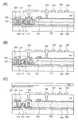
도 6(A)∼도 6(C)는 본 발명의 액정표시장치의 단면도.6 (A) to 6 (C) are cross-sectional views of a liquid crystal display device of the present invention.
도 7(A)∼도 7(C)는 본 발명의 액정표시장치의 단면도.7 (A) to 7 (C) are sectional views of a liquid crystal display device of the present invention.
도 8(A)∼도 8(C)는 본 발명의 액정표시장치의 단면도.8 (A) to 8 (C) are cross-sectional views of a liquid crystal display device of the present invention.
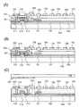
도 9(A)∼도 9(C)는 본 발명의 액정표시장치의 단면도.9 (A) to 9 (C) are sectional views of a liquid crystal display device of the present invention.
도 10(A)∼도 10(C)는 본 발명의 액정표시장치의 단면도.10 (A) to 10 (C) are sectional views of a liquid crystal display device of the present invention.
도 11(A)∼도 11(C)는 본 발명의 액정표시장치의 단면도.11 (A) to 11 (C) are sectional views of a liquid crystal display device of the present invention.
도 12(A)∼도 12(C)는 본 발명의 액정표시장치의 단면도.12 (A) to 12 (C) are sectional views of a liquid crystal display device of the present invention.
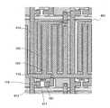
도 13은 본 발명의 액정표시장치의 상면도.13 is a top view of a liquid crystal display device of the present invention.
도 14는 본 발명의 액정표시장치의 상면도.14 is a top view of the liquid crystal display device of the present invention.
도 15는 본 발명의 액정표시장치의 단면도.15 is a sectional view of a liquid crystal display device of the present invention.
도 16은 본 발명의 액정표시장치의 단면도.16 is a sectional view of a liquid crystal display device of the present invention.
도 17은 본 발명의 액정표시장치의 단면도.17 is a sectional view of a liquid crystal display device of the present invention.
도 18은 본 발명의 액정표시장치의 단면도.18 is a sectional view of the liquid crystal display device of the present invention.
도 19는 본 발명의 액정표시장치의 단면도.19 is a cross-sectional view of a liquid crystal display device of the present invention.
도 20은 본 발명의 액정표시장치의 단면도.20 is a sectional view of a liquid crystal display device of the present invention.
도 21은 본 발명의 액정표시장치의 단면도.21 is a sectional view of a liquid crystal display device of the present invention.
도 22는 본 발명의 액정표시장치의 단면도.22 is a sectional view of the liquid crystal display device of the present invention.
도 23은 본 발명의 액정표시장치의 단면도.23 is a sectional view of the liquid crystal display device of the present invention.
도 24는 본 발명의 액정표시장치의 단면도.24 is a sectional view of the liquid crystal display device of the present invention.
도 25는 본 발명의 액정표시장치의 단면도.25 is a sectional view of a liquid crystal display device of the present invention.
도 26은 본 발명의 액정표시장치의 단면도.26 is a sectional view of the liquid crystal display device of the present invention.
도 27은 본 발명의 액정표시장치의 단면도.27 is a sectional view of the liquid crystal display device of the present invention.
도 28은 본 발명의 액정표시장치의 단면도.28 is a sectional view of a liquid crystal display device of the present invention.
도 29는 본 발명의 액정표시장치의 단면도.29 is a sectional view of a liquid crystal display device of the present invention.
도 30은 본 발명의 액정표시장치의 단면도.30 is a sectional view of the liquid crystal display device of the present invention.
도 31은 본 발명의 액정표시장치의 단면도.31 is a cross-sectional view of a liquid crystal display device of the present invention.
도 32는 본 발명의 액정표시장치의 단면도.32 is a sectional view of the liquid crystal display device of the present invention.
도 33은 본 발명의 액정표시장치의 단면도.33 is a sectional view of a liquid crystal display device of the present invention.
도 34는 본 발명의 액정표시장치의 단면도.34 is a cross-sectional view of a liquid crystal display device of the present invention.
도 35는 본 발명의 액정표시장치의 단면도.35 is a sectional view of the liquid crystal display device of the present invention.
도 36은 본 발명의 액정표시장치의 단면도.36 is a sectional view of the liquid crystal display device of the present invention.
도 37은 본 발명의 액정표시장치의 단면도.37 is a sectional view of the liquid crystal display device of the present invention.
도 38은 본 발명의 액정표시장치의 단면도.38 is a sectional view of the liquid crystal display device of the present invention.
도 39는 본 발명의 액정표시장치의 단면도.39 is a sectional view of the liquid crystal display device of the present invention.
도 40은 본 발명의 액정표시장치의 단면도.40 is a sectional view of a liquid crystal display device of the present invention.
도 41은 본 발명의 액정표시장치의 단면도.41 is a sectional view of the liquid crystal display device of the present invention.
도 42는 본 발명의 액정표시장치의 단면도.42 is a sectional view of the liquid crystal display device of the present invention.
도 43은 본 발명의 액정표시장치의 단면도.43 is a sectional view of the liquid crystal display device of the present invention.
도 44는 본 발명의 액정표시장치의 단면도.44 is a sectional view of the liquid crystal display device of the present invention.
도 45는 본 발명의 액정표시장치의 단면도.45 is a sectional view of the liquid crystal display device of the present invention.
도 46은 본 발명의 액정표시장치의 단면도.46 is a sectional view of the liquid crystal display device of the present invention.
도 47은 본 발명의 액정표시장치의 단면도.47 is a sectional view of a liquid crystal display device of the present invention.
도 48은 본 발명의 액정표시장치의 단면도.48 is a sectional view of the liquid crystal display device of the present invention.
도 49는 본 발명의 액정표시장치의 단면도.49 is a sectional view of a liquid crystal display device of the present invention.
도 50은 본 발명의 액정표시장치의 단면도.50 is a sectional view of the liquid crystal display device of the present invention.
도 51은 본 발명의 액정표시장치의 단면도.51 is a sectional view of a liquid crystal display device of the present invention.
도 52는 본 발명의 액정표시장치의 단면도.52 is a sectional view of the liquid crystal display device of the present invention.
도 53은 본 발명의 액정표시장치의 단면도.53 is a sectional view of the liquid crystal display device of the present invention.
도 54는 본 발명의 액정표시장치의 단면도.54 is a sectional view of the liquid crystal display device of the present invention.
도 55는 본 발명의 액정표시장치의 단면도.55 is a sectional view of a liquid crystal display device of the present invention.
도 56은 본 발명의 액정표시장치의 단면도.56 is a sectional view of the liquid crystal display device of the present invention.
도 57은 본 발명의 액정표시장치의 단면도.57 is a sectional view of a liquid crystal display device of the present invention.
도 58은 본 발명의 액정표시장치의 단면도.58 is a sectional view of the liquid crystal display device of the present invention.
도 59는 본 발명의 액정표시장치의 단면도.59 is a sectional view of the liquid crystal display device of the present invention.
도 60은 본 발명의 액정표시장치의 단면도.60 is a sectional view of a liquid crystal display device of the present invention.
도 61은 본 발명의 액정표시장치의 단면도.61 is a sectional view of the liquid crystal display device of the present invention.
도 62는 본 발명의 액정표시장치의 단면도.62 is a sectional view of the liquid crystal display device of the present invention.
도 63은 본 발명의 액정표시장치의 단면도.63 is a sectional view of a liquid crystal display device of the present invention.
도 64는 본 발명의 액정표시장치의 단면도.64 is a sectional view of a liquid crystal display device of the present invention.
도 65는 본 발명의 액정표시장치의 단면도.65 is a sectional view of the liquid crystal display device of the present invention.
도 66은 본 발명의 액정표시장치의 단면도.66 is a sectional view of the liquid crystal display device of the present invention.
도 67은 본 발명의 액정표시장치의 단면도.67 is a sectional view of the liquid crystal display device of the present invention.
도 68은 본 발명의 액정표시장치의 단면도.68 is a sectional view of the liquid crystal display device of the present invention.
도 69는 본 발명의 액정표시장치의 단면도.69 is a sectional view of the liquid crystal display device of the present invention.
도 70은 본 발명의 액정표시장치의 단면도.70 is a sectional view of a liquid crystal display device of the present invention.
도 71은 본 발명의 액정표시장치의 단면도.71 is a sectional view of the liquid crystal display device of the present invention.
도 72는 본 발명의 액정표시장치의 단면도.72 is a sectional view of the liquid crystal display device of the present invention.
도 73은 본 발명의 액정표시장치의 단면도.73 is a sectional view of the liquid crystal display device of the present invention.
도 74는 본 발명의 액정표시장치의 단면도.74 is a sectional view of the liquid crystal display device of the present invention.
도 75는 본 발명의 액정표시장치의 단면도.75 is a sectional view of a liquid crystal display device of the present invention.
도 76은 본 발명의 액정표시장치의 단면도.76 is a sectional view of the liquid crystal display device of the present invention.
도 77(A)∼도 77(C)는 본 발명의 액정표시장치를 나타내는 도면.Figs. 77 (A) to 77 (C) are views showing a liquid crystal display device of the present invention. Fig.
도 78은 본 발명의 액정표시장치의 도면.78 is a view of a liquid crystal display device of the present invention.
도 79는 본 발명의 액정표시장치의 단면도.79 is a sectional view of a liquid crystal display device of the present invention.
도 80은 본 발명의 액정표시장치의 단면도.80 is a sectional view of a liquid crystal display device of the present invention.
도 81은 본 발명의 액정표시장치의 단면도.81 is a sectional view of the liquid crystal display device of the present invention.
도 82는 본 발명의 액정표시장치의 단면도.82 is a sectional view of the liquid crystal display device of the present invention.
도 83은 본 발명의 액정표시장치의 단면도.83 is a sectional view of the liquid crystal display device of the present invention.
도 84는 본 발명의 액정표시장치의 단면도.84 is a sectional view of the liquid crystal display device of the present invention.
도 85는 본 발명의 액정표시장치의 단면도.85 is a sectional view of the liquid crystal display device of the present invention.
도 86은 본 발명의 액정표시장치의 단면도.86 is a sectional view of the liquid crystal display device of the present invention.
도 87은 본 발명의 액정표시장치의 단면도.87 is a sectional view of the liquid crystal display device of the present invention.
도 88은 본 발명의 액정표시장치의 단면도.88 is a sectional view of the liquid crystal display device of the present invention.
도 89는 본 발명의 액정표시장치의 단면도.89 is a sectional view of the liquid crystal display device of the present invention.
도 90은 본 발명의 액정표시장치의 단면도.90 is a sectional view of the liquid crystal display device of the present invention.
도 91은 본 발명의 액정표시장치의 단면도.91 is a sectional view of the liquid crystal display device of the present invention.
도 92는 본 발명의 액정표시장치의 단면도.92 is a sectional view of the liquid crystal display device of the present invention.
도 93은 본 발명의 액정표시장치의 단면도.93 is a sectional view of the liquid crystal display device of the present invention.
도 94는 본 발명의 액정표시장치의 단면도.94 is a sectional view of the liquid crystal display device of the present invention.
도 95는 본 발명의 액정표시장치의 단면도.95 is a sectional view of a liquid crystal display device of the present invention.
도 96은 본 발명의 액정표시장치의 단면도.96 is a sectional view of the liquid crystal display device of the present invention.
도 97은 본 발명의 액정표시장치의 단면도.97 is a sectional view of the liquid crystal display device of the present invention.
도 98은 본 발명의 액정표시장치의 단면도.98 is a sectional view of the liquid crystal display device of the present invention.
도 99는 본 발명의 액정표시장치의 단면도.99 is a sectional view of a liquid crystal display device of the present invention.
도 100은 본 발명의 액정표시장치의 단면도.100 is a sectional view of a liquid crystal display device of the present invention.
도 101은 본 발명의 액정표시장치의 단면도.101 is a sectional view of a liquid crystal display device of the present invention.
도 102는 본 발명의 액정표시장치의 단면도.102 is a sectional view of a liquid crystal display device of the present invention.
도 103은 본 발명의 액정표시장치의 단면도.103 is a sectional view of a liquid crystal display device of the present invention.
도 104는 본 발명의 액정표시장치의 단면도.104 is a sectional view of the liquid crystal display device of the present invention.
도 105는 본 발명의 액정표시장치의 단면도.105 is a sectional view of the liquid crystal display device of the present invention.
도 106은 본 발명의 액정표시장치를 나타내는 도면.106 is a view showing a liquid crystal display device of the present invention.
도 107(A)∼도 107(D)는 본 발명의 액정표시장치를 나타내는 도면.107 (A) to 107 (D) are views showing a liquid crystal display device of the present invention.
도 108은 본 발명의 액정표시장치를 나타내는 도면.108 is a view showing a liquid crystal display device of the present invention.
도 109(A) 및 도 109(B)는 본 발명의 액정표시장치의 상면도 및 단면도.109 (A) and 109 (B) are a top view and a cross-sectional view of a liquid crystal display device of the present invention.
도 110(A) 및 도 110(B)는 본 발명의 액정표시장치를 나타내는 도면.Figs. 110 (A) and 110 (B) are views showing a liquid crystal display device of the present invention. Fig.
도 111(A)∼도 111(H)는 본 발명을 적용한 전자 기기들의 예를 나타내는 도면.111 (A) to 111 (H) are views showing examples of electronic appliances to which the present invention is applied.
도 112(A)∼도 112(C)는 본 발명의 액정표시장치를 나타내는 도면.Figures 112 (A) to 112 (C) illustrate a liquid crystal display of the present invention.
본 발명은 액정표시장치에 관한 것이다. 특히, 본 발명은 시야각이 넓은 액정표시장치에 관한 것이다.The present invention relates to a liquid crystal display device. More particularly, the present invention relates to a liquid crystal display device having a wide viewing angle.
표시장치에는 자기발광 표시장치와 비발광(수광) 표시장치가 있고, 액정표시장치는 비발광 표시장치의 가장 대표적인 것이다. 그리고, 액정표시장치에서의 액정 구동방법에는, 기판에 대하여 수직으로 전압을 인가하는 종전계 방식과, 기판에 대하여 대략 평행으로 전압을 인가하는 횡전계 방식이 있다. 종전계 방식과 횡전계 방식은 서로 이점 및 결점을 가지고 있다. 예를 들어, TN 방식으로 대표되는 종전계 방식에 비하여, 횡전계 방식은 광시야각, 고콘트라스트, 고계조 표시와 같은 특성을 가지고, 모니터나 텔레비전용으로 사용되고 있다. 이러한 액정표시장치는 액정 분야에서 공존하고 있고, 제품 개발이 행해지고 있다. 또한, 횡전계 방식용의 액정 재료와, 종전계 방식용의 액정 재료 각각이 개발되고 있고, 전압 인가 방향에 따라 다른 재료 특성을 가진다.The display device includes a self-light-emitting display device and a non-light-emitting (light-receiving) display device, and the liquid crystal display device is the most representative of non-light-emitting display devices. In the liquid crystal driving method in the liquid crystal display device, there are an old system system in which a voltage is applied perpendicularly to a substrate and a transverse system system in which a voltage is applied substantially parallel to the substrate. The conventional system and the transverse electric system have advantages and disadvantages. For example, the transverse electric field system has characteristics such as a wide viewing angle, a high contrast, and a high gradation display, and is used for a monitor or a television, compared with the current system represented by the TN system. Such a liquid crystal display device coexists in the liquid crystal field, and product development has been carried out. Further, a liquid crystal material for a transverse electric field system and a liquid crystal material for an electric current system have been developed, and have different material properties depending on the voltage application direction.
또한, 횡전계 방식의 액정표시장치에는, IPS(In-Plane Switching) 방식과 FFS(Fringe Field Switching) 방식이 있다. IPS 방식에서는, 빗살 형상이나 슬릿이 들어간 화소 전극과, 빗살 형상이나 슬릿이 들어간 공통 전극이 교호로 배치되어 있고, 화소 전극과 공통 전극과의 사이에 기판에 대략 평행인 방향의 전계를 발생시켜, 액정표시장치를 구동하는 방식이다(일본국 공개특허공고 평 9-105918호 공보 참조). 한편, FFS 방식에서는, 화소부 전체에 형성된 평면 형상의 공통 전극 위에, 빗살 형상이나 슬릿이 들어간 화소 전극이 배치되어 있다. 그리고, 화소 전극과 공통 전극과의 사이에 기판에 대략 평행인 방향의 전계를 발생시켜, 액정표시 장치를 구동하는 방식이다.In addition, IPS (In-Plane Switching) method and FFS (Fringe Field Switching) method are available for liquid crystal display devices of the transverse electric field system. In the IPS system, a pixel electrode having a comb-like shape or a slit and a common electrode having a comb-like shape or a slit are alternately arranged, and an electric field in a direction substantially parallel to the substrate is generated between the pixel electrode and the common electrode, Thereby driving a liquid crystal display device (see Japanese Patent Laid-Open Publication No. 9-105918). On the other hand, in the FFS system, a pixel electrode having a comb shape or a slit is arranged on a planar common electrode formed over the entire pixel portion. An electric field in a direction substantially parallel to the substrate is generated between the pixel electrode and the common electrode to drive the liquid crystal display device.
FFS 방식의 액정표시장치는 고투과율, 광시야각, 저소비전력을 가지고, 크로스토크(crosstalk)가 없다(Ultra-FFS TFT-LCD with Super Image Quality and Fast Response Time 2001 SID P.484-487 참조).The FFS type liquid crystal display device has high transmittance, wide viewing angle, low power consumption, and does not have crosstalk (see Ultra-FFS TFT-LCD with Super Image Quality and
종래의 횡전계 방식으로 대표되는 횡전계 방식의 액정표시장치에서는, 액정 재료에 걸리는 전계가 충분하지 않았다. 이것은 공통 전극이나 화소 전극 바로 위에 있는 액정 재료에 전계가 잘 걸리지 않았기 때문이다.In the liquid crystal display device of the transverse electric field system typified by the conventional transverse electric field system, the electric field applied to the liquid crystal material was not sufficient. This is because the electric field is not applied to the liquid crystal material directly above the common electrode or the pixel electrode.
또한, IPS 방식이나 FFS 방식과 같은 횡전계 방식을 사용한 광시야각 기술은 주로 텔레비전용으로 사용되고 있었으므로, 투과형에 한정되어 있었다. 그러나, 보다 소비전력을 낮추는 경우나 옥외에서도 사용하고자 하는 경우에는, 반사형이나 반투과형으로 할 필요가 있었다. 그러나, 반사형이나 반투과형은 TN 방식으로 대표되는 종전계 방식을 사용하여 실현되고 있었다.Further, since the wide viewing angle technique using the transverse electric field system such as the IPS system or the FFS system is mainly used for television, it is limited to the transmission type. However, when it is desired to lower the power consumption or to use it outdoors, it is necessary to use a reflection type or a semi-transmission type. However, the reflection type or the semi-transmission type has been realized by using an electric current system represented by a TN system.
따라서, 본 발명은, 횡전계 방식의 액정표시장치에서 액정 재료에 걸리는 전계를 충분한 것으로 하는 구성을 제공하는 것을 목적으로 한다.Therefore, it is an object of the present invention to provide a structure in which a sufficient electric field is applied to a liquid crystal material in a liquid crystal display device of a transverse electric field system.
또한, 본 발명은, 광시야각이고, 표시 화면을 보는 각도에 의존한 색감의 변화가 적고, 실내에서도 옥외에서도 양호하게 시인(視認)할 수 있는 화상을 표시할 수 있는 액정표시장치를 제공하는 것을 과제로 한다.It is another object of the present invention to provide a liquid crystal display device capable of displaying an image which is a wide viewing angle and has less change in color depending on the angle at which the display screen is viewed and which can be visually well viewed both indoors and outdoors We will do it.
상기 과제를 감안하여, 본 발명은, 횡전계 방식에서, 1쌍의 전극이 아니라 다수 쌍의 전극을 사용하여 액정 재료에 전계를 인가하는 것을 특징으로 한다. 1쌍의 전극은 빗살 형상의 공통 전극과, 빗살 형상의 화소 전극을 포함한다. 다른 쌍의 전극은 화소부에 형성된 공통 전극과, 빗살 형상의 화소 전극을 포함한다. 화소부에 제공된 공통 전극은 박막트랜지스터 이외의 영역에 걸쳐 제공될 수 있다. 또한, 화소부에 제공된 공통 전극은 빗살 형상으로 하여도 상관없다. 이와 같은 액정표시장치에서는, 1쌍의 전극에 더하여, 다른 쌍의 전극을 사용함으로써, 액정 재료에 인가되는 전계를 제어할 수 있다.In view of the above problems, the present invention is characterized in that, in the transverse electric field system, an electric field is applied to the liquid crystal material by using not a pair of electrodes but a plurality of pairs of electrodes. The pair of electrodes includes a comb-shaped common electrode and a comb-shaped pixel electrode. The other pair of electrodes includes a common electrode formed in the pixel portion and a comb-shaped pixel electrode. The common electrode provided in the pixel portion can be provided over an area other than the thin film transistor. The common electrode provided in the pixel portion may be a comb-like shape. In such a liquid crystal display device, the electric field applied to the liquid crystal material can be controlled by using another pair of electrodes in addition to the pair of electrodes.
또한, 본 발명의 액정표시장치는 광의 투과에 의해 표시를 행하는 제1 영역과, 광의 반사에 의해 표시를 행하는 제2 영역을 포함한다. 또한, 액정층은, 액정층보다도 하방에 제공된 2개의 액정 소자 전극들 사이에 전위차가 발생했을 때 전극면에 평행한, 즉, 기판에 평행한 면 내에서 회전하는 액정 분자를 포함하고 있다.Further, the liquid crystal display device of the present invention includes a first region for performing display by transmission of light and a second region for performing display by reflection of light. The liquid crystal layer includes liquid crystal molecules that are parallel to the electrode surface, that is, rotate in a plane parallel to the substrate when a potential difference is generated between the two liquid crystal device electrodes provided below the liquid crystal layer.
또한, 본 발명에서, "전극면에 평행한 회전"이란, 인간의 눈으로 인식할 수 없는 정도의 편차를 가지는 평행한 회전을 의미한다. 바꿔말하면, "전극면에 평행한 회전"이란, 전극면에 평행한 벡터 성분을 주로 포함하지만 전극면에 수직인 벡터 성분도 약간 가지는 회전을 의미한다.Further, in the present invention, "rotation parallel to the electrode surface" means parallel rotation having a degree of deviation that can not be perceived by the human eye. In other words, "rotation parallel to the electrode surface" means rotation having mainly a vector component parallel to the electrode surface but also a vector component perpendicular to the electrode surface.
액정층(801)에 포함된 액정 분자(802)는, 액정층(801)의 하방에 제공된 전극(803)과 전극(804) 사이에 전위차가 생겼을 때, 횡방향 전계의 영향에 의해 회전한다. 액정 분자(802)가 회전함에 따라, 도 77(A)에 나타낸 상태가 도 77(B)에 나타낸 상태로 변화하거나, 또는 도 77(B)에 나타낸 상태가 도 77(A)에 나타낸 상태 로 변화한다. 도 77(A) 및 도 77(B)는 단면도를 나타낸다. 이 회전을 평면 위에서 본 것이 도 77(C)의 화살표로 나타내어진다.The
마찬가지로, 액정층(9801)에 포함된 액정 분자(9802)는, 액정층(9801)의 하방에 제공된 전극(9803)과 전극(9805)과의 사이, 및 전극(9804)과 전극(9805)과의 사이에 전위차가 생겼을 때, 횡방향 전계의 영향에 의해 회전하고, 액정 분자(9802)가 회전함에 따라, 도 112(A)에 나타낸 상태가 도 112(B)에 나타낸 상태로 변화하거나, 또는 도 112(B)에 나타낸 상태가 도 112(A)에 나타낸 상태로 변화한다. 도 112(A) 및 도 112(B)는 단면도를 나타낸다. 이 회전을 평면 위에서 본 것이 도 112(C)의 화살표로 나타내어진다.The
또한, 전극(803)과 전극(804)의 위치 관계 등은 도 77(A)∼도 77(C)에 나타낸 것에 한정되지 않는다.The positional relationship between the
마찬가지로, 전극(9803)과 전극(9804)과 전극(9805)의 위치 관계 등은 도 112(A)∼도 112(C)에 나타낸 것에 한정되지 않는다.Similarly, the positional relationship between the
상기한 제1 영역에서, 액정층의 하방에 제공된 한 쌍의 전극은 상이한 층에 제공된 전극들을 포함한다. 제1 영역에서, 액정층의 하방에는 액정 소자의 2개의 전극이 제공되어 있고, 이들 전극은 상이한 층에 제공되어 있다. 그리고, 이들 전극 중 어느 한쪽을 반사체로서 기능시키거나, 또는 이들 전극과 겹치도록 반사체를 제공함으로써, 광을 반사시킨다. 또한, 제2 영역에서, 액정층의 하방에는 액정 소자의 2개의 전극이 제공되어 있고, 이들 전극 모두를 투광성으로 하고, 같은 층 위에 또는 절연층을 사이에 두고 다른 층 위에 제공하고 있다.In the first region, a pair of electrodes provided below the liquid crystal layer include electrodes provided in different layers. In the first region, two electrodes of the liquid crystal element are provided below the liquid crystal layer, and these electrodes are provided in different layers. Then, either of these electrodes functions as a reflector, or reflects light by providing a reflector so as to overlap these electrodes. In the second region, two electrodes of a liquid crystal element are provided below the liquid crystal layer, and both of these electrodes are made transparent to light and provided on the same layer or on another layer with an insulating layer therebetween.
이하에, 본 발명의 구체적인 구성을 나타낸다.Hereinafter, a specific configuration of the present invention will be shown.
본 발명의 일 양태는, 제1 공통 전극과, 그 제1 공통 전극 위에 제공된 절연층과, 그 절연층 위에 제공된 화소 전극 및 제2 공통 전극과, 그 화소 전극 및 제2 공통 전극 위에 제공된 액정 재료를 포함하고, 상기 화소 전극과 상기 제1 공통 전극과의 사이의 전계, 및 상기 화소 전극과 상기 제2 공통 전극과의 사이의 전계에 의해, 상기 액정 재료의 기울기(tilting)가 제어되는 것을 특징으로 하는 액정표시장치이다.According to an aspect of the present invention, there is provided a liquid crystal display comprising: a first common electrode; an insulating layer provided on the first common electrode; a pixel electrode and a second common electrode provided on the insulating layer; Characterized in that the tilting of the liquid crystal material is controlled by an electric field between the pixel electrode and the first common electrode and an electric field between the pixel electrode and the second common electrode In the liquid crystal display device.
본 발명의 다른 양태는, 절연 기판과, 그 절연 기판 위에 형성된 박막트랜지스터와, 그 박막트랜지스터의 반도체층과 동일 층에 제공된 제1 공통 전극과, 그 제1 공통 전극을 덮도록 제공된 절연층과, 그 절연층 위에 제공된 화소 전극 및 제2 공통 전극과, 그 화소 전극 및 제2 공통 전극 위에 제공된 액정 재료를 포함하고, 상기 화소 전극은 상기 박막트랜지스터에 의해 제어되고, 상기 제1 공통 전극과 상기 제2 공통 전극은 전기적으로 접속되어 있고, 상기 화소 전극과 상기 제1 공통 전극과의 사이의 전계, 및 상기 화소 전극과 상기 제2 공통 전극과의 사이의 전계에 의해, 액정 재료의 기울기가 제어되는 것을 특징으로 하는 액정표시장치이다.A thin film transistor formed on the insulating substrate; a first common electrode provided on the same layer as the semiconductor layer of the thin film transistor; an insulating layer provided to cover the first common electrode; A pixel electrode and a second common electrode provided on the insulating layer, and a liquid crystal material provided on the pixel electrode and the second common electrode, the pixel electrode being controlled by the thin film transistor, The second common electrode is electrically connected and the slope of the liquid crystal material is controlled by the electric field between the pixel electrode and the first common electrode and the electric field between the pixel electrode and the second common electrode And a liquid crystal display device.
본 발명의 다른 양태는, 절연 기판과, 그 절연 기판 위에 형성된 박막트랜지스터와, 그 박막트랜지스터의 소스 전극 및 드레인 전극과 동일 층에 제공된 제1 공통 전극과, 그 제1 공통 전극에 접속된 도전층과, 상기 제1 공통 전극 및 상기 도전층 위에 제공된 절연층과, 그 절연층 위에 제공된 화소 전극 및 제2 공통 전극 과, 상기 화소 전극 및 상기 제2 공통 전극 위에 제공된 액정 재료를 포함하고, 상기 화소 전극과 상기 제1 공통 전극과의 사이의 전계, 및 상기 화소 전극과 상기 제2 공통 전극과의 사이의 전계에 의해, 상기 액정 재료의 기울기가 제어되는 것을 특징으로 하는 액정표시장치이다.A thin film transistor formed on the insulating substrate; a first common electrode provided on the same layer as the source electrode and the drain electrode of the thin film transistor; and a second common electrode provided on the first common electrode, An insulating layer provided on the first common electrode and the conductive layer; a pixel electrode and a second common electrode provided on the insulating layer; and a liquid crystal material provided on the pixel electrode and the second common electrode, Wherein the slope of the liquid crystal material is controlled by an electric field between the electrode and the first common electrode and an electric field between the pixel electrode and the second common electrode.
본 발명의 다른 양태는, 절연 기판과, 그 절연 기판 위에 형성된 박막트랜지스터와, 그 박막트랜지스터의 반도체층과 동일 층에 제공된 제1 공통 전극과, 그 제1 공통 전극에 접속된 도전층과, 상기 제1 공통 전극 및 상기 도전층 위에 제공된 절연층과, 그 절연층 위에 제공된 화소 전극 및 제2 공통 전극과, 상기 화소 전극 및 상기 제2 공통 전극 위에 제공된 액정 재료를 포함하고, 상기 화소 전극과 상기 제1 공통 전극과의 사이의 전계, 및 상기 화소 전극과 상기 제2 공통 전극과의 사이의 전계에 의해, 상기 액정 재료의 기울기가 제어되는 것을 특징으로 하는 액정표시장치이다.According to another aspect of the present invention, there is provided a semiconductor device comprising: an insulating substrate; a thin film transistor formed on the insulating substrate; a first common electrode provided on the same layer as the semiconductor layer of the thin film transistor; a conductive layer connected to the first common electrode; A pixel electrode and a second common electrode provided on the insulating layer, and a liquid crystal material provided on the pixel electrode and the second common electrode, wherein the pixel electrode and the second common electrode are provided on the first common electrode and the conductive layer, Wherein a slope of the liquid crystal material is controlled by an electric field between the pixel electrode and the first common electrode and an electric field between the pixel electrode and the second common electrode.
본 발명의 구성에서, 상기 박막트랜지스터는 결정성 반도체층을 가질 수 있다.In the configuration of the present invention, the thin film transistor may have a crystalline semiconductor layer.
본 발명의 구성에서, 상기 제1 공통 전극과 상기 박막트랜지스터 위에 제공된 패시베이션층과, 그 패시베이션층을 사이에 두고 상기 제1 공통 전극 위에 제공된 컬러 필터와, 상기 패시베이션층을 사이에 두고 상기 박막트랜지스터 위에 제공된 블랙 매트릭스가 더 포함될 수 있다.In the structure of the present invention, the passivation layer provided on the first common electrode and the thin film transistor, the color filter provided on the first common electrode with the passivation layer therebetween, and the passivation layer on the thin film transistor The provided black matrix may further be included.
본 발명의 구성에서, 상기 제1 공통 전극과 상기 박막트랜지스터 위에 제공된 패시베이션층과, 그 패시베이션층을 사이에 두고 상기 제1 공통 전극 및 상기 박막트랜지스터 위에 제공된 컬러 필터와, 상기 절연 기판에 대향하여 제공된 대향 기판과, 상기 박막트랜지스터 위에 제공된 블랙 매트릭스가 더 포함될 수 있다.In the configuration of the present invention, a color filter provided over the first common electrode and the thin film transistor with a passivation layer provided over the first common electrode and the thin film transistor, a passivation layer provided between the first common electrode and the thin film transistor, A counter substrate, and a black matrix provided on the thin film transistor.
본 발명의 구성에서, 상기 박막트랜지스터 위에 제공된 패시베이션층과, 그 패시베이션층 위에 제공된 컬러 필터와, 그 컬러 필터 위에 제공된 제1 공통 전극과, 상기 패시베이션층을 사이에 두고 상기 박막트랜지스터 위에 제공된 블랙 매트릭스가 더 포함될 수 있다.In the configuration of the present invention, a passivation layer provided on the thin film transistor, a color filter provided on the passivation layer, a first common electrode provided on the color filter, and a black matrix provided on the thin film transistor with the passivation layer therebetween . ≪ / RTI >
본 발명의 다른 양태는, 절연 기판과, 그 절연 기판 위에 형성된 게이트 전극과, 상기 게이트 전극과 동일 층에 형성된 제1 공통 전극과, 상기 게이트 전극 및 상기 제1 공통 전극을 덮도록 제공된 절연층과, 그 절연층을 사이에 두고 상기 게이트 전극 위에 제공된 반도체층과, 그 반도체층에 형성된 소스 전극 및 드레인 전극과, 상기 제1 공통 전극에 접하도록 상기 소스 전극 및 드레인 전극과 동일 층에 제공된 도전층과, 상기 소스 전극과 드레인 전극 중 하나에 접속된 화소 전극과, 상기 도전층을 사이에 두고 상기 제1 공통 전극에 접속된 제2 공통 전극과, 상기 화소 전극 및 상기 제2 공통 전극 위에 제공된 액정 재료를 포함하고, 상기 화소 전극과 상기 제1 공통 전극과의 사이의 전계, 및 상기 화소 전극과 상기 제2 공통 전극과의 사이의 전계에 의해, 상기 액정 재료의 기울기가 제어되는 것을 특징으로 하는 액정표시장치이다.According to another aspect of the present invention, there is provided a semiconductor device comprising an insulating substrate, a gate electrode formed on the insulating substrate, a first common electrode formed on the same layer as the gate electrode, and an insulating layer provided to cover the gate electrode and the first common electrode A source electrode and a drain electrode formed on the semiconductor layer, and a conductive layer provided on the same layer as the source electrode and the drain electrode to be in contact with the first common electrode, A pixel electrode connected to one of the source electrode and the drain electrode, a second common electrode connected to the first common electrode with the conductive layer therebetween, and a second common electrode connected to the pixel electrode and the second common electrode, And an electric field between the pixel electrode and the first common electrode and an electric field between the pixel electrode and the second common electrode, And the inclination of the liquid crystal material is controlled.
본 발명의 다른 양태는, 절연 기판과, 그 절연 기판 위에 형성된 게이트 전극과, 그 게이트 전극과 동일 층에 형성된 도전층과, 그 도전층에 접하여 제공된 제1 공통 전극과, 상기 게이트 전극 및 상기 제1 공통 전극을 덮도록 제공된 절연 층과, 그 절연층을 사이에 두고 상기 게이트 전극 위에 제공된 반도체층과, 그 반도체층에 형성된 소스 전극 및 드레인 전극과, 상기 소스 전극과 드레인 전극 중 하나에 접속된 화소 전극과, 상기 도전층을 사이에 두고 상기 제1 공통 전극에 접속된 제2 공통 전극과, 상기 화소 전극 및 제2 공통 전극 위에 제공된 액정 재료를 포함하고, 상기 화소 전극과 상기 제1 공통 전극과의 사이의 전계, 및 상기 화소 전극과 상기 제2 공통 전극과의 사이의 전계에 의해, 상기 액정 재료의 기울기가 제어되는 것을 특징으로 하는 액정표시장치이다.According to another aspect of the present invention, there is provided a semiconductor device comprising: an insulating substrate; a gate electrode formed on the insulating substrate; a conductive layer formed on the same layer as the gate electrode; 1. A semiconductor device, comprising: an insulating layer provided to cover one common electrode; a semiconductor layer provided on the gate electrode with the insulating layer therebetween; a source electrode and a drain electrode formed on the semiconductor layer; A pixel electrode, a second common electrode connected to the first common electrode through the conductive layer, and a liquid crystal material provided on the pixel electrode and the second common electrode, wherein the pixel electrode and the first common electrode , And the slope of the liquid crystal material is controlled by an electric field between the pixel electrode and the second common electrode Display device.
본 발명의 구성에서, 상기 반도체층은 비정질 반도체층을 가질 수 있다.In the configuration of the present invention, the semiconductor layer may have an amorphous semiconductor layer.
본 발명의 구성에서, 상기 제1 공통 전극 위에 제공된 패시베이션층과, 그 패시베이션층을 사이에 두고 상기 제1 공통 전극 위에 제공된 컬러 필터와, 상기 소스 전극 및 드레인 전극 위에 제공된 불랙 매트릭스가 더 포함될 수 있다.In the configuration of the present invention, a passive layer provided on the first common electrode, a color filter provided on the first common electrode with the passivation layer therebetween, and a flavor matrix provided on the source electrode and the drain electrode .
본 발명의 구성에서, 상기 제1 공통 전극 및 상기 게이트 전극 위에 제공된 패시베이션층과, 상기 소스 전극 및 드레인 전극 위와 상기 패시베이션층을 사이에 두고 상기 제1 공통 전극 위에 제공된 컬러 필터와, 상기 절연 기판에 대향하여 제공된 대향 기판과, 그 대향 기판 위에 제공된 불랙 매트릭스가 더 포함될 수 있다.In the structure of the present invention, a passivation layer provided on the first common electrode and the gate electrode, a color filter provided on the first common electrode with the passivation layer interposed therebetween on the source electrode and the drain electrode, A counter substrate provided opposite thereto, and a block matrix provided on the counter substrate.
본 발명의 구성에서, 상기 화소 전극은 빗살 형상을 가질 수 있다.In the configuration of the present invention, the pixel electrode may have a comb shape.
본 발명의 구성에서, 상기 제1 공통 전극은 빗살 형상을 가질 수 있다.In the configuration of the present invention, the first common electrode may have a comb shape.
본 발명의 구성에서, 상기 제2 공통 전극은 빗살 형상을 가질 수 있다.In the configuration of the present invention, the second common electrode may have a comb shape.
본 발명의 구성에서, 상기 화소 전극은 투광성 재료로 형성될 수도 있다.In the configuration of the present invention, the pixel electrode may be formed of a light-transmitting material.
본 발명의 구성에서, 상기 제1 공통 전극은 투광성 재료로 형성될 수도 있 다.In the configuration of the present invention, the first common electrode may be formed of a light-transmitting material.
본 발명의 구성에서, 상기 제2 공통 전극은 투광성 재료로 형성될 수도 있다.In the configuration of the present invention, the second common electrode may be formed of a light-transmitting material.
본 발명에 의하면, 2쌍 이상의 전극을 사용하여 액정 재료에 충분한 전계를 인가할 수 있다. 그리고, 2쌍의 전극에 의해 발생된 전계에 의해, 액정 재료의 기울기를 제어함으로써, 계조 표시를 행할 수 있다.According to the present invention, it is possible to apply a sufficient electric field to the liquid crystal material by using two or more pairs of electrodes. By controlling the tilt of the liquid crystal material by the electric field generated by the two pairs of electrodes, gray scale display can be performed.
또한, 본 발명에 의하면, 시야각이 넓고, 표시 화면을 보는 각도에 의존한 색감의 변화가 적고, 태양광이 비추어진 실외 및 어두운 실내(또는 밤의 실외)에서도 양호하게 시인(視認)할 수 있는 화상이 제공될 수 있다.Further, according to the present invention, it is possible to provide a display device which is wide in view angle, has little change in color depending on the angle at which the display screen is viewed, and can be visually confirmed in the outdoors and dark room (or outdoors at night) An image can be provided.
이하에, 본 발명의 실시형태를 도면에 의거하여 설명한다. 그러나, 본 발명은 많은 다른 양태로 실시할 수 있고, 본 발명의 취지 및 그 범위에서 벗어나는 일 없이 그 형태 및 상세한 사항을 다양하게 변경할 수 있다는 것은 당업자라면 용이하게 이해할 수 있다. 따라서, 본 발명이 본 실시형태의 기재 내용에 한정하여 해석되는 것은 아니다. 또한, 실시형태를 설명하기 위한 모든 도면에서, 동일 부분 또는 같은 기능을 가지는 부분에는 동일 부호를 붙이고, 그 반복 설명은 생략한다.DESCRIPTION OF THE PREFERRED EMBODIMENTS Hereinafter, embodiments of the present invention will be described with reference to the drawings. It will be apparent, however, to one skilled in the art that the present invention may be embodied with many other modes, and that various changes in form and details may be made therein without departing from the spirit and scope of the invention. Therefore, the present invention is not limited to the content of the present embodiment. In all the drawings for explaining the embodiments, the same reference numerals are given to the same parts or portions having the same functions, and the repetitive description thereof will be omitted.
또한, 본 발명에서, 적용 가능한 트랜지스터의 종류에 한정은 없고, 비정질 규소나 다결정 규소로 대표되는 비(非)단결정 반도체막을 사용한 박막트랜지스터(TFT), 반도체 기판이나 SOI 기판을 사용하여 형성되는 MOS형 트랜지스터, 접합형 트랜지스터, 바이폴러 트랜지스터, 유기 반도체나 탄소 나노튜브를 사용한 트랜지스터, 그 외의 트랜지스터를 적용할 수 있다. 또한, 트랜지스터가 배치되는 기 판의 종류에 한정은 없고, 단결정 기판, SOI 기판, 유리 기판 등에 트랜지스터를 형성할 수도 있다.In addition, the present invention is not limited to the types of transistors to which the present invention can be applied, and can be applied to a thin film transistor (TFT) using a non-single crystal semiconductor film typified by amorphous silicon or polycrystalline silicon, a MOS type A transistor, a junction transistor, a bipolar transistor, an organic semiconductor, a transistor using carbon nanotubes, or other transistors can be applied. The type of the substrate on which the transistor is disposed is not limited, and a transistor may be formed on a single crystal substrate, an SOI substrate, a glass substrate, or the like.
또한, 본 발명에서, 접속은 전기적 접속과 같은 의미이다. 따라서, 본 발명에서 개시하는 구성에서, 소정의 접속 관계를 가지는 소자들 사이에, 전기적 접속을 가능하게 하는 다른 소자(예를 들어, 다른 소자, 스위치, 트랜지스터, 용량 소자, 저항 소자, 다이오드 등)가 배치될 수도 있다.Further, in the present invention, connection is synonymous with electrical connection. Therefore, in the configuration disclosed in the present invention, another element (for example, another element, a switch, a transistor, a capacitor, a resistor, a diode, or the like) that enables electrical connection is provided between elements having a predetermined connection relationship. May be disposed.
또한, 본 발명에서 나타내는 스위치는 전기적 스위치나 기계적 스위치와 같은 어느 것이라도 좋다. 전류 흐름을 제어할 수 있는 것이라면, 무엇이든 좋다. 그 스위치는 트랜지스터이어도 좋고, 다이오드이어도 좋고, 그들을 조합시킨 논리회로이어도 좋다. 따라서, 스위치로서 트랜지스터를 사용하는 경우, 그 트랜지스터는 단순한 스위치로서 동작하기 때문에, 트랜지스터의 극성(도전형)은 특별히 한정되는 것은 아니다. 그러나, 오프 전류가 적은 것이 바람직한 경우, 오프 전류가 적은 극성의 트랜지스터를 사용하는 것이 바람직하다. 오프 전류가 적은 트랜지스터로서는, LDD 영역을 가진 트랜지스터, 멀티게이트 구조를 가진 트랜지스터 등이 있다. 또한, 스위치로서 기능하는 트랜지스터의 소스 단자의 전위가 저전위측 전원(Vss, Vgnd, 0 V 등)에 가까운 상태에서 동작하는 경우에는 n채널형 트랜지스터를 사용하고, 반대로, 소스 단자의 전위가 고전위측 전원(Vdd 등)에 가까운 상태에서 동작하는 경우에는 p채널형 트랜지스터를 사용하는 것이 바람직하다. 이것은, 게이트-소스 전압의 절대값을 크게 할 수 있기 때문에, 트랜지스터가 스위치로서 작용하기 쉽기 때문이다. 또한, n채널형 트랜지스터와 p채널형 트랜지스터 모두를 사용하여 CMOS형 스위치로 하여도 좋다.Further, the switch shown in the present invention may be any of an electrical switch and a mechanical switch. Anything that can control the current flow is good. The switch may be a transistor, a diode, or a logic circuit combining them. Therefore, when a transistor is used as a switch, the transistor operates as a simple switch, so that the polarity (conductive type) of the transistor is not particularly limited. However, in the case where it is preferable that the off current is small, it is preferable to use a transistor of polarity with a small off current. A transistor having an LDD region and a transistor having a multi-gate structure can be used as the transistor having a small off current. When an operation is performed in a state in which the potential of the source terminal of the transistor serving as a switch is close to the low potential side power supply (Vss, Vgnd, 0 V, etc.), an n-channel transistor is used. Conversely, It is preferable to use a p-channel transistor when operating in a state close to the upper power supply (Vdd or the like). This is because the transistor can function as a switch because the absolute value of the gate-source voltage can be increased. The n-channel type transistor and the p-channel type transistor may be used as a CMOS type switch.
또한, 앞에서 설명한 바와 같이, 본 발명에서의 트랜지스터는 어떠한 타입의 트랜지스터이어도 좋고, 어떠한 기판 위에 형성되어 있어도 좋다. 따라서, 화소를 구동하는 회로들이 모두 유리 기판 위에 형성되어 있어도 좋고, 플라스틱 기판에 형성되어 있어도 좋고, 단결정 기판에 형성되어 있어도 좋고, SOI 기판 위에 형성되어 있어도 좋고, 어떤 다른 기판 위에 형성되어 있어도 좋다. 또는, 화소를 구동하는 회로들 중 일부가 어느 한 기판 위에 형성되고, 다른 일부가 다른 기판 위에 형성되어 있어도 좋다. 즉, 화소를 구동하는 회로들 전부가 동일 기판 위에 형성되어 있지 않아도 좋다. 예를 들어, 화소부와 게이트선 구동회로는 유리 기판 위에 TFT를 사용하여 형성되고, 신호선 구동회로(또는 그의 일부)는 단결정 기판 위에 형성되고, 그의 IC 칩을 COG(Chip On Glass)에 의해 유기 기판에 접속하여도 좋다. 또는 그 IC 칩을 TAB(Tape Auto Bonding)나 프린트 기판을 사용하여 유리 기판에 접속하여도 좋다.Further, as described above, the transistor in the present invention may be any type of transistor or may be formed on any substrate. Therefore, all the circuits for driving the pixels may be formed on the glass substrate, on the plastic substrate, on the single crystal substrate, on the SOI substrate, or on any other substrate. Alternatively, some of the circuits for driving the pixels may be formed on one substrate, and another part may be formed on another substrate. That is, not all the circuits for driving the pixels need be formed on the same substrate. For example, the pixel portion and the gate line driver circuit are formed by using a TFT on a glass substrate, the signal line driver circuit (or a part thereof) is formed on a single crystal substrate, and the IC chip thereof is formed by COG (Chip On Glass) It may be connected to a substrate. Alternatively, the IC chip may be connected to a glass substrate by using TAB (Tape Auto Bonding) or a printed board.
또한, 화소에 배치되는 소자는 특정 소자에 한정되지 않는다. 화소에 배치되는 표시 소자의 예로서는, EL(electroluminescence) 소자(OLED(유기 발광 다이오드), 유기 EL 소자, 무기 EL 등이라고도 함)나 전계 방출 디스플레이(FED)에 사용되는 소자, FED의 일종인 SED(Surface-conduction Electron-emitter Display), 액정 디스플레이(LCD), GLV(글레팅 라이트 밸브), 플라즈마 디스플레이(PDP), 전자 페이퍼 디스플레이, 디지털 마이크로미러 디바이스(DMD), 압전 세라믹 디스플레이 등, 어떠한 표시 소자이어도 좋다.Further, the element arranged in the pixel is not limited to a specific element. Examples of the display element disposed in the pixel include elements used in an EL (electroluminescence) element (OLED (organic light emitting diode), organic EL element, inorganic EL or the like) or a field emission display (FED) Any display device, such as a surface-conduction electron-emitter display, a liquid crystal display (LCD), a glazing light valve (GLV), a plasma display (PDP), an electronic paper display, a digital micromirror device (DMD) good.
또한, 반도체장치란, 트랜지스터나 다이오드 등의 반도체 소자를 가지는 장치를 말한다. 또한, 표시장치란, 액정 소자나 EL 소자 등의 표시 소자를 가지는 장치를 말한다. 또한, 발광장치란, EL 소자나 FED에 사용되는 것과 같은 발광 소자를 가지는 장치를 말한다.The term " semiconductor device " refers to a device having semiconductor elements such as transistors and diodes. The display device refers to a device having a display element such as a liquid crystal element or an EL element. The light emitting device refers to a device having a light emitting element such as an EL element or a FED.
[실시형태 1][Embodiment 1]
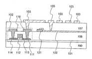
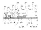
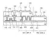
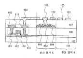
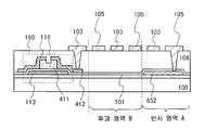
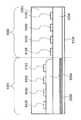
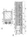
본 발명의 액정표시장치의 일 형태에 대하여 도 78을 참조하여 설명한다. 액정표시장치에서는, 복수의 화소가 매트릭스 형태로 제공되어 있고, 일 화소의 단면 구조의 일 예가 도 78에 도시되어 있다.One embodiment of the liquid crystal display device of the present invention will be described with reference to Fig. In a liquid crystal display device, a plurality of pixels are provided in a matrix form, and one example of a cross-sectional structure of one pixel is shown in Fig.
도 78에 도시된 바와 같이, 화소는 광을 반사시켜 표시를 행하는 부분(반사부)(1001)과 광을 투과시켜 표시를 행하는 부분(투과부)(1002)을 가진다. 각각의 영역에서, 화소 전극으로서 기능하는 전극과, 공통 전극으로서 기능하는 전극이 제공되어 있다.As shown in Fig. 78, a pixel has a portion (reflection portion) 1001 for reflecting light to perform display and a portion (transmission portion) 1002 for transmitting light to display. In each region, an electrode functioning as a pixel electrode and an electrode functioning as a common electrode are provided.
화소 전극으로서 기능하는 전극은 빗살 형상이나 슬릿 형상을 가진다. 한편, 공통 전극으로서 기능하는 전극은 평면 형상을 가지는 부분과, 빗살 형상이나 슬릿 형상을 가지는 부분을 포함한다. 그러나, 이러한 조합에 한정되는 것은 아니다.The electrode functioning as the pixel electrode has a comb shape or a slit shape. On the other hand, the electrode functioning as the common electrode includes a portion having a planar shape and a portion having a comb shape or a slit shape. However, the present invention is not limited to such a combination.
그리고, 화소 전극으로서 기능하는 전극과, 공통 전극으로서 기능하는 전극에 전압이 공급되면, 전계가 발생한다. 그 전계는 기판에 평행인 성분을 많이 포함하고 있다. 그리고, 액정 분자는 그 전계에 따라 기판에 평행한 면 내에서 회전한다. 그것에 의해, 광의 투과율이나 반사율이 제어될 수 있어, 계조를 표시할 수 있다.Then, when a voltage is supplied to an electrode functioning as a pixel electrode and an electrode functioning as a common electrode, an electric field is generated. The electric field contains many components parallel to the substrate. Then, the liquid crystal molecules rotate in a plane parallel to the substrate in accordance with the electric field. Thereby, the transmittance and reflectance of light can be controlled, and gradation can be displayed.
공통 전극으로서 기능하는 전극이 다수 제공되어 있는 경우에는, 절연층에 개구부(콘택트 홀)를 형성하거나, 전극들을 중첩시켜 서로 전기적으로 접속하는 것이 바람직하다.When a plurality of electrodes functioning as common electrodes are provided, it is preferable to form openings (contact holes) in the insulating layer or to electrically connect the electrodes overlapping each other.
또한, 화소 전극으로서 기능하는 전극과 공통 전극으로서 기능하는 전극이 절연층을 사이에 두고 배치되어 있는 경우, 그 중첩 부분이 용량으로서 기능할 수 있다. 이 용량은 화상 신호를 보유하기 위한 보유 용량으로서 기능할 수 있다.Further, in the case where the electrode functioning as the pixel electrode and the electrode functioning as the common electrode are arranged with the insulating layer interposed therebetween, the overlapping portion can function as the capacitance. This capacitance can function as a storage capacitor for holding an image signal.
광을 반사시켜 표시를 행하는 부분(반사부)(1001)에서는, 반사용 전극이 제공되어 있고, 이 반사용 전극에 의해 광을 반사시켜 표시가 행해진다. 반사용 전극은 공통 전극을 겸할 수도 있고, 이 경우, 반사용 전극은 공통 전극과 접속되어, 전압이 공급될 수도 있다. 물론, 반사용 전극과 공통 전극이 따로따로 제공될 수도 있다. 이와 같이 반사용 전극과 공통 전극이 따로 존재하는 경우에는, 반사용 전극에는 전압이 공급되지 않거나 다른 전압이 공급될 수도 있다.In a portion (reflective portion) 1001 for reflecting light to perform display, a reflection electrode is provided, and light is reflected by the reflection electrode to perform display. The counter electrode may also serve as a common electrode. In this case, the counter electrode may be connected to the common electrode, and a voltage may be supplied. Of course, the counter electrode and the common electrode may be provided separately. In the case where the counter electrode and the common electrode are separately provided as described above, no voltage may be supplied to the counter electrode or a different voltage may be supplied.
광을 투과시켜 표시를 행하는 부분(투과부)(1002)에서는, 투광성 전극이 제공될 수 있고, 따라서, 광을 투과시키거나 또는 전극의 간극을 통과시켜 표시가 행해진다. 투명 전극은 공통 전극을 겸할 수도 있고, 이 경우, 투명 전극은 공통 전극에 접속되어, 전압이 공급될 수 있다. 물론, 투광성 전극과 공통 전극을 서로 다른 전극으로 할 수도 있다. 이와 같이 투명 전극과 공통 전극이 따로 존재하는 경우에는, 투명 전극에는 전압이 공급되지 않거나, 다른 전압이 공급될 수도 있다. 또한, 투명 전극은 화소 전극을 겸할 수도 있다.In the portion (transmissive portion) 1002 through which light is transmitted to perform display, a light-transmissive electrode can be provided, and therefore, light is transmitted or displayed by passing through the gap of the electrode. The transparent electrode may also serve as a common electrode. In this case, the transparent electrode may be connected to the common electrode so that a voltage can be supplied. Of course, the light-transmitting electrode and the common electrode may be different electrodes. In the case where the transparent electrode and the common electrode exist separately as described above, no voltage may be supplied to the transparent electrode, or a different voltage may be supplied. The transparent electrode may also serve as a pixel electrode.
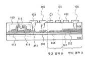
다음에, 도 78에 나타낸 구성에 대하여 설명한다. 반사부(1001)에서는, 액정 소자의 전극(9103)과 액정 소자의 전극(9305)이 절연층(9204, 9304)을 사이에 두고 중첩되어 있다. 또한, 투과부(1002)에서는, 액정 소자의 전극(9103)과 액정 소자의 전극(9104)이 절연층(9304)을 사이에 두고 중첩되어 있다.Next, the configuration shown in Fig. 78 will be described. In the
또한, 반사부(1001)와 투과부(1002)에서, 액정 소자의 전극(9305)과 액정 소자의 전극(9303)은 교호로 배치되어 있다.In the
액정 소자의 전극(9103, 9105)은 빗살 형상으로 형성되어 있고, 액정 소자의 전극(9305, 9104)은 면 형상으로 형성되어 있다. 그러나, 이것에 한정되는 것은 아니다. 액정 소자의 전극(9305)과 액정 소자의 전극(9104)이 슬릿과 같은 간극을 가지거나, 구멍을 가지거나, 빗살 형상으로 될 수도 있다.The
액정 소자의 전극(9103)이 화소 전극으로서 기능하고, 액정 소자의 전극(9305), 액정 소자의 전극(9104), 액정 소자의 전극(9105)은 공통 전극으로서 기능한다. 그러나, 이것에 한정되는 것은 아니고, 액정 소자의 전극(9103)이 공통 전극으로서 기능하고, 액정 소자의 전극(9305), 액정 소자의 전극(9104), 액정 소자의 전극(9105)이 화소 전극으로서 기능하여도 좋다.The
공통 전극들 각각은 절연층에 콘택트 홀을 형성하거나 그 전극들을 서로 중첩시킴으로써 전기적으로 접속되는 것이 바람직하다.Each of the common electrodes is preferably electrically connected by forming a contact hole in the insulating layer or overlapping the electrodes with each other.
액정 소자의 전극(9305)은 도전성을 가짐과 동시에 광을 반사하는 재료로 형성되어 있다. 따라서, 액정 소자의 전극(9305)은 반사용 전극으로서 기능한다. 또한, 액정 소자의 전극(9104)은 투광성을 가짐과 동시에 광을 투과하는 재료로 형 성되어 있다. 따라서, 액정 소자의 전극(9104)은 투명 전극으로서 기능한다.The
액정 소자의 전극(9103, 9105)은 도전성을 가짐과 동시에 광을 투과하는 재료로 형성되어 있는 것이 바람직하다. 이것은, 그 전극들이 광을 투과할 수 있을 때 화상을 표시하는 부분에 기여할 수 있기 때문이다. 그러나, 액정 소자의 전극(9103, 9105)은 광을 반사하는 재료로 형성되어도 좋다. 그 경우에는, 예를 들어, 투과부(1002)에서도 광을 반사하기 때문에, 투과부(1002)가 반사부로서 기능할 수 있다.It is preferable that the
또한, 액정 소자의 전극(9103, 9105)은 동시에 형성되는 것이 바람직하다. 액정 소자의 전극(9103, 9105)을 동시에 형성함으로써, 프로세스를 간략화할 수 있고, 마스크(레티클) 수를 저감할 수 있고, 비용을 낮출 수 있기 때문이다. 그러나, 이것에 한정되는 것은 아니고, 액정 소자의 전극(9103, 9105)을 따로따로 형성하여도 좋다. 그 경우, 액정 소자의 전극(9103, 9105) 중의 어느 하나가 투과성을 가지고, 다른 쪽이 반사성을 가지는 것이 가능하다.It is also preferable that the
또한, 화소 전극으로서 기능하는 전극(액정 소자의 전극(9103))과 공통 전극으로서 기능하는 전극(액정 소자의 전극(9305, 9104, 9105))이 절연층을 사이에 두고 배치되어 있는 경우, 겹침 부분이 용량으로서 기능할 수 있고, 그 용량이 화상 신호를 보유하기 위한 보유 용량으로서 기능할 수 있다.When electrodes (liquid crystal element electrodes 9103) that function as pixel electrodes and electrodes (liquid
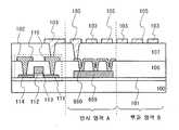
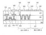
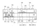
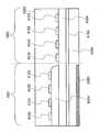
도 78 및 도 79에 도시된 바와 같이, 액정 소자의 전극(9103)과 액정 소자의 전극(9305) 사이, 액정 소자의 전극(9103)과 액정 소자의 전극(9105) 사이에 전위차가 발생했을 때, 액정층(9303)의 액정 분자(9303a, 9303b)는 액정 소자의 전 극(9103, 9305, 9104)의 표면에 평행인 방향으로(즉, 기판에 평행인 면에서) 회전한다. 따라서, 액정층(9303)을 통과하는 광의 양이 제어될 수 있다. 즉, 광의 편광 상태가 제어될 수 있고, 기판의 외부에 제공되어 있는 편광판을 통과하는 광의 양이 제어될 수 있다. 도 79는 도 77(A) 및 도 112(A)에 대응한다. 도 79에 도시된 액정 분자(9303a, 9303b)가 도 77(A), 도 77(B), 도 112(A), 도 112(B)에 도시된 액정 분자와 마찬가지로 회전한다. 외측으로부터 액정표시장치 내로 입사한 광은 액정층(9303)을 통과한 후, 액정 소자의 전극(9103)과 절연층(9204, 9304)을 통과하고, 액정 소자의 전극(9305)에서 반사한 후, 절연층(9204, 9304)과 액정 소자의 전극(9103)을 통과하여 액정표시장치로부터 나온다.When a potential difference is generated between the
또한, 도 79의 전극(9004)은 도 78의 액정 소자의 전극(9305, 9104)에 상당하고, 도 79의 절연층(9005)은 도 78의 절연층(9204, 9304)에 상당한다.The
도 79에 도시된 바와 같이, 공통 전극으로서 기능하는 전극이 화소 전극으로서 기능하는 전극의 하방에 횡방향이나 비스듬한 방향(상향 경사방향과 하향 경사방향을 포함)으로 제공되어 있기 때문에, 영역(9002)과 영역(9003)에서, 기판에 평행한 전계 성분이 보다 많이 생기게 된다. 그 결과, 시야각 특성이 더욱 향상된다.As shown in Fig. 79, since the electrode functioning as the common electrode is provided in the lateral direction or in the oblique direction (including the upward inclination direction and the downward inclination direction) below the electrode functioning as the pixel electrode, In the
또한, 절연층(9204, 9304)은 굴절률 이방성을 거의 가지고 있지 않기 때문에, 그곳을 광이 통과할 때 편광 상태가 변화하지 않는다.Since the insulating
또한, 광을 반사시켜 표시를 행하는 부분(반사부)(1001)과 광을 투과시켜 표시를 행하는 부분(투과부)(1002)에서, 광로에 컬러 필터가 제공되어, 소망의 색을 가지는 광을 생성한다. 이와 같이 하여, 각 화소로부터 사출된 광이 합성되어 화상을 표시하게 된다.In addition, a color filter is provided in an optical path in a portion (reflective portion) 1001 for reflecting light to perform display and a portion (transmissive portion) 1002 for performing display by transmitting light to generate light having a desired color do. In this way, light emitted from each pixel is combined to display an image.
따라서, 컬러 필터는 액정층(9303) 위에 배치되는 대향 기판 위에 제공될 수도 있고, 액정 소자의 전극(9103)의 상방에 제공될 수도 있다. 또는, 컬러 필터는 절연층(9304) 위에 제공되거나 또는 그 절연층의 일부로서 제공될 수도 있다.Therefore, the color filter may be provided on the counter substrate disposed on the
또한, 컬러 필터와 마찬가지로, 블랙 매트릭스가 제공될 수도 있다.Also, like the color filter, a black matrix may be provided.
또한, 광을 반사시켜 표시를 행하는 부분(반사부)(1001)에서는 광이 액정층(9303)을 2회 통과한다. 즉, 외광이 대향 기판측으로부터 액정층(9303)으로 들어가고, 액정 소자의 전극(9305)에 의해 반사되어, 다시, 액정층(9303)으로 들어가 대향 기판측을 통해 밖으로 나오므로, 광이 액정층(9303)을 2회 통과하게 된다.Further, light passes through the
한편, 광을 투과시켜 표시를 행하는 부분(투과부)(1002)에서는 광이 액정 소자의 전극(9104)을 통과하여 액정층(9303)으로 들어가 대향 전극으로부터 나온다. 즉, 광이 액정층(9303)을 1회 통과한다.On the other hand, in the portion (transmissive portion) 1002 through which light is transmitted to perform display, light passes through the
여기서, 액정층(9303)은 굴절률 이방성을 가지고 있기 때문에, 광이 액정층(9303)을 통과하는 거리에 따라, 광의 편광 상태가 바뀌게 된다. 따라서, 화상을 표시하는 경우에, 바르게 표시할 수 없게 되어 버린다. 따라서, 광의 편광 상태를 조정할 필요가 있다. 그것을 위한 방법으로서, 광을 반사시켜 표시를 행하는 부분(반사부)(1001)의 액정층(9303)의 두께(소위 셀 갭)를 얇게 함으로써, 광이 2회 통과하여도, 광이 액정층(9303)을 통과하는 거리가 너무 길어지는 것을 방지할 수 있다.Here, since the
또한, 절연층(9204, 9304)은 굴절률 이방성을 거의 가지고 있지 않기 때문에, 그곳을 광이 통과하여도, 편광 상태는 변화하지 않는다. 따라서, 절연층(9204, 9304)의 유무나 두께 등은 큰 영향을 주지 않는다.Since the insulating
따라서, 액정층(9303)의 두께(소위 셀 갭)를 얇게 하기 위해, 그 두께를 조정하는 막을 배치할 수도 있다. 도 78에서는, 절연층(9204)이 그러한 막에 상당한다. 즉, 광을 반사시켜 표시를 행하는 부분(반사부)(1001)에서, 절연층(9204)은 액정층의 두께를 조정하기 위해 제공되는 층이다. 절연층(9204)을 제공함으로써 반사부(1001)에서의 액정층의 두께를 투과부(1002)에서의 액정층의 두께보다 얇게 할 수 있다.Therefore, in order to reduce the thickness (so-called cell gap) of the
또한, 반사부(1001)에서의 액정층(9303)의 두께는 투과부(1002)에서의 액정층(9303)의 두께의 2분의 1인 것이 바람직하다. 여기서, 2분의 1이란, 인간의 눈으로 인식할 수 없는 정도의 편차를 포함할 수도 있다.It is preferable that the thickness of the
그러나, 광이 항상 기판에 수직인 방향, 즉, 법선 방향으로만 입사하는 것은 아니다. 광이 비스듬하게 입사하는 경우도 있다. 따라서, 그러한 경우를 총합하여, 반사부(1001)와 투과부(1002)에서 광이 통과하는 거리가 실질적으로 대략 같은 정도가 될 필요가 있다. 따라서, 반사부(1001)에서의 액정층(9303)의 두께는 투과부(1002)에서의 액정층(9303)의 두께의 대략 3분의 1 이상, 3분의 2 이하가 되는 것이 바람직하다.However, the light is not always incident in the direction perpendicular to the substrate, that is, in the normal direction. In some cases, light is incident at an angle. Therefore, by summing up such cases, it is necessary that the distance through which the light passes through the
이와 같이, 액정 소자의 전극(9103)이 제공되어 있는 기판측 위에, 액정층(9303)의 두께를 조정하는 막을 배치하면, 막의 형성이 쉽게 될 수 있다. 즉, 액정 소자의 전극(9103)이 제공되어 있는 기판측에는, 다양한 배선이나 전극이나 막이 형성되어 있다. 따라서, 그러한 배선이나 전극이나 막을 사용하여 액정층(9303)의 두께를 조정하는 막을 형성할 수 있으므로, 그다지 어려움 없이 막을 형성할 수 있다. 또한, 동일 공정에서, 다른 기능을 가지는 막을 형성할 수 있으므로, 프로세스를 간략화할 수 있고, 비용을 절감할 수 있다.As described above, if a film for adjusting the thickness of the
이상과 같은 구성을 가지는 본 발명의 액정표시장치는 시야각이 넓고, 또한, 표시 화면을 보는 각도에 의존한 색감의 변화가 적고, 또한, 태양이 비추어지는 실외에서도 어두운 실내(또는 밤의 옥외)에서도 양호하게 시인되는 화상을 제공할 수 있다.The liquid crystal display of the present invention having the above-described configuration has a wide viewing angle, and also has little change in color depending on the angle at which the display screen is viewed. In addition, even in the outdoors where the sun is shining, It is possible to provide an image which is well recognized.
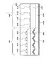
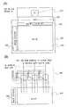
도 78에서는 액정 소자의 전극(9305)과 액정 소자의 전극(9104)이 동일 평면에 배치되어 있지만, 이것에 한정되는 것은 아니고, 상이한 평면에 형성될 수도 있다.In Fig. 78, the
또한, 도 78에서, 액정 소자의 전극(9305)과 액정 소자의 전극(9104)이 서로 떨어져 배치되어 있지만, 이것에 한정되는 것은 아니고, 그들 전극(9305, 9104)이 서로 접촉하여 배치되어도 좋고, 하나의 전극으로 형성되어도 좋다. 또는, 액정 소자의 전극(9305)과 액정 소자의 전극(9104)은 서로 전기적으로 접속되어 있어도 좋다.78, the
또한, 도 78에서, 액정층(9303)의 두께를 조정하기 위한 막으로서, 절연층(9204)이 배치되어 있지만, 이것에 한정되는 것은 아니고, 액정층(9303)의 두께를 조정하기 위한 막이 대향 기판측에 배치될 수도 있다.78, the insulating
또한, 액정층(9303)의 두께를 얇게 하기 위해, 막이 배치되어 있지만, 역으로, 액정층(9303)의 두께를 두껍게 하기 위해, 소정의 영역에서 막을 제거하도록 하여도 좋다.In addition, the film is disposed in order to reduce the thickness of the
또한, 반사용 전극은 평탄한 표면을 가질 수 있지만, 요철 표면을 가지는 것이 바람직하다. 요철 표면을 가지고 있음으로써, 광을 확산시켜 반사시킬 수 있다. 그 결과, 광을 분산시킬 수 있고, 휘도를 향상시킬 수 있다.Further, although the reflection electrode may have a flat surface, it is preferable that the reflection electrode has a surface with irregularities. By having a roughened surface, light can be diffused and reflected. As a result, the light can be dispersed and the luminance can be improved.
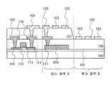
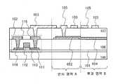
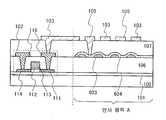
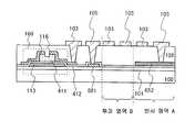
또한, 도 80에 도시된 바와 같이, 투과부(1002)에서, 액정 소자의 전극(9104)은 없어도 좋다.In addition, as shown in Fig. 80, in the
그 경우에는, 도 81에 도시된 바와 같이, 액정 소자의 전극(9105)과 액정 소자의 전극(9103) 사이에 전압을 인가하여, 액정 분자(9303a, 9303b)를 제어한다.In this case, as shown in Fig. 81, a voltage is applied between the
이와 같이, 투과부(1002)에 액정 소자의 전극(9104)을 배치하지 않기 때문에, 그만큼 프로세스를 간략화할 수 있고, 마스크(레티클) 수를 저감할 수 있고, 비용을 절감할 수 있다.Since the
[실시형태 2][Embodiment 2]
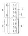
실시형태 1의 것과 다른 구성의 본 발명의 액정표시장치의 예에 대하여 설명한다. 또한, 실시형태 1의 것과 동일한 기능을 가지는 부분에 대해서는 같은 부호를 사용하여 설명한다.An example of a liquid crystal display device of the present invention having a configuration different from that of
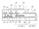
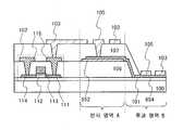
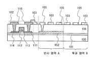
도 82는 액정 소자의 전극(9305)과 액정 소자의 전극(9104)이 적층되어 있는 점에서 도 78의 액정표시장치와 다른 액정표시장치의 예를 나타내고 있다. 액정 소자의 전극(9305)과 액정 소자의 전극(9104)을 모두 동일 전위로 하고자 하는 경 우, 이와 같이 적층시켜 서로 전기적으로 접속시킬 수도 있다.Fig. 82 shows an example of a liquid crystal display device different from the liquid crystal display device of Fig. 78 in that the
또한, 액정 소자의 전극(9104)이 액정 소자의 전극(9305) 아래에 배치되어 있지만, 이것에 한정되는 것은 아니고, 액정 소자의 전극(9104)이 액정 소자의 전극(9305) 위에 배치되어도 좋다.Note that the
또한, 액정 소자의 전극(9104)이 액정 소자의 전극(9305) 아래의 전역에 걸쳐 배치되어 있지만, 이것에 한정되는 것은 아니고, 액정 소자의 전극(9104)이 액정 소자의 전극(9305)의 일부의 아래나 위에 배치될 수도 있다.Although the
또한, 액정 소자의 전극(9104)이 액정 소자의 전극(9305) 아래의 전역에 걸쳐 배치되어 있는 경우, 액정 소자의 전극(9305)과 액정 소자의 전극(9104)을 1장의 마스크를 사용하여 형성할 수 있다. 통상, 액정 소자의 전극(9305)과 액정 소자의 전극(9104)은 각각 서로 다른 마스크를 사용하여 형성되지만, 이 경우에는, 하프톤(halftone), 그레이톤(graytone) 등의 마스크를 사용하고, 레지스트의 두께를 영역에 따라 바꿈으로써, 1장의 마스크로 액정 소자의 전극(9305)과 액정 소자의 전극(9104)을 형성할 수 있다. 그 결과, 프로세스를 간략화할 수 있고, 공정 수를 줄일 수 있고, 마스크 수(레티클 수)를 줄일 수 있다. 따라서, 비용을 절감할 수 있게 된다.When the
도 83에서는, 액정 소자의 전극(9305)과 액정 소자의 전극(9104)을 서로 부분적으로 중첩시켜 전기적으로 접속하고 있는 액정표시장치를 나타내고 있다. 이와 같은 구성에서는, 액정 소자의 전극(9305)과 액정 소자의 전극(9104)이 전기적으로 접속될 수도 있다.Fig. 83 shows a liquid crystal display device in which the
또한, 액정 소자의 전극(9104)이 액정 소자의 전극(9305) 위에 서로 접하도록 배치되어 있지만, 이것에 한정되는 것은 아니다. 액정 소자의 전극(9305)이 액정 소자의 전극(9104) 위에 서로 접하도록 배치되어도 좋다.Further, although the
이와 같이, 액정 소자의 전극(9305) 위의 넓은 영역에서 액정 소자의 전극(9104)을 배치하지 않음으로써, 그곳에서의 광의 손실을 저감할 수 있다.In this way, by not disposing the
도 84에서는, 액정 소자의 전극(9305)과 액정 소자의 전극(9104)이 절연층(9306)을 사이에 두고 상이한 층에 제공되어 있다. 또한, 도 85에서와 같이, 액정 소자의 전극(9305, 9104)을 각각 다른 층에 제공하여도 좋다.In Fig. 84, the
이와 같이, 액정 소자의 전극(9305)과 액정 소자의 전극(9104)을 다른 층에 배치하면, 반사부(1001)에서의 액정 소자의 전극(9305)과 액정 소자의 전극(9104) 사이의 거리가 투과부(1002)에서의 거리와 대략 같게 된다. 따라서, 반사부(1001)와 투과부(1002)에서, 전극들의 간격을 같은 정도로 할 수 있다. 전계의 인가 및 강도는 전극들 사이이의 거리에 따라 변화하기 때문에, 전극들 사이의 간격을 반사부(1001)와 투과부(1002)에서 같은 정도로 함으로써, 액정층(9303)에 인가하는 전계도 같은 정도로 할 수 있기 때문에, 액정 분자의 제어가 정확하게 행해질 수 있다. 또한, 반사부(1001)와 투과부(1002)에서 액정 분자의 회전 정도가 대략 같아지므로, 액정표시장치를 투과형으로 하여 화상을 표시하거나 보는 경우이든, 반사형으로 하여 화상을 표시하거나 보는 경우이든, 대략 동일한 계조를 가진 화상을 볼 수 있다.When the
또한, 액정 소자의 전극(9104)은 액정 소자의 전극(9305) 아래의 영역 전체 에 배치되어 있지만, 이것에 한정되는 것은 아니다. 액정 소자의 전극(9104)이 적어도 투과부(1002)에 배치되어 있으면 된다.Note that the
또한, 절연층(16)에 콘택트 홀을 형성하여, 액정 소자의 전극(9104)과 액정 소자의 전극(9305)을 접속하여도 좋다.A contact hole may be formed in the insulating layer 16 to connect the
도 85는 액정 소자의 전극(9305)이 액정 소자의 전극(9104)보다 아래의 층(액정층(9303)으로부터 먼 쪽 층)에 제공되어 있는 점에서 도 84의 액정표시장치와 다른 액정표시장치의 예를 나타낸다.85 is different from the liquid crystal display of Fig. 84 in that the
또한, 액정 소자의 전극(9104)이 반사부(1001)에도 형성되어 있지만, 이것에 한정되는 것은 아니다. 액정 소자의 전극(9104)이 적어도 투과부(1002)에 배치되어 있으면 된다.Further, although the
또한, 액정 소자의 전극(9104)이 반사부(1001)에도 형성되어 있는 경우, 반사부(1001)에서도 액정 소자의 전극(9104)과 액정 소자의 전극(9103) 사이의 전압에 따라 액정층(9303)을 제어한다. 그 경우에는, 액정 소자의 전극(9305)은 반사용 전극으로만 기능하고, 액정 소자의 전극(9104)은 반사부(1001)에서의 공통 전극으로서 기능한다.When the
따라서, 그 경우, 액정 소자의 전극(9305)에 공급되는 전압은 임의적이 된다. 액정 소자의 전극(9104) 또는 액정 소자의 전극(9103)과 동일한 전압을 액정 소자의 전극(9305)에 공급할 수도 있다. 그 경우, 액정 소자의 전극(9305)과 액정 소자의 전극(9104)과의 사이에 용량이 형성되고, 그 용량은 화상 신호를 보유하기 위한 보유 용량으로서 기능할 수도 있다.Therefore, in that case, the voltage supplied to the
또한, 절연층(16)에 콘택트 홀을 형성하여, 액정 소자의 전극(9104)과 액정 소자의 전극(9305)을 접속하여도 좋다.A contact hole may be formed in the insulating layer 16 to connect the
도 86에서는, 반사부(1001)의 액정 소자의 전극(9305)과 투과부(1002)의 액정 소자의 전극(9103, 9105)이 절연층(9304) 위에 형성되어 있다. 그리고, 절연층(9204)은 액정 소자의 전극(9305) 위에 형성되고, 그 위에, 반사부의 액정 소자의 전극(9103, 9105)이 형성되어 있다. 액정 소자의 전극(9104)은 절연층(9304) 아래에 형성되어 있다.86, the
또한, 액정 소자의 전극(9104)이 반사부(1001)에도 형성되어 있지만, 이것에 한정되지 않는다. 액정 소자의 전극(9104)이 적어도 투과부(1002)에 배치되어 있으면 된다.Further, although the
또한, 절연층(9304)에 콘택트 홀을 형성하여, 액정 소자의 전극(9104)과 액정 소자의 전극(9305)을 접속하여도 좋다.A contact hole may be formed in the insulating
또한, 도 93에 도시된 바와 같이, 투과부(1002)에는 액정 소자의 전극(9104)이 없어도 된다.In addition, as shown in Fig. 93, the
그 경우, 도 81에 도시된 바와 같이, 액정 소자의 전극(9105)과 액정 소자의 전극(9103) 사이에 전압을 인가하여, 액정 분자(9303a, 9303b)를 제어한다.In this case, as shown in Fig. 81, a voltage is applied between the
이와 같이, 투과부(1002)에 액정 소자의 전극(9104)을 배치하지 않기 때문에, 그만큼 프로세스를 간략화할 수 있고, 마스크(레티클) 수를 저감할 수 있고, 비용을 낮출 수 있다.Since the
또한, 도 78∼도 86, 및 도 93에서는, 전극 표면의 요철을 나타내지 않았지 만, 액정 소자의 전극(9103, 9305, 9104, 9105)의 표면이 평탄한 것에 한정되는 것은 아니고, 그들 표면에 요철을 가지고 있어도 좋다.78 to 86 and 93 do not show concavities and convexities on the electrode surface, the surfaces of the
또한, 도 78∼도 86, 및 도 93에서는, 절연층(9204, 9304, 9306)의 표면의 요철을 나타내지 않았지만, 절연층(9204, 9304, 9306)의 표면이 평탄한 것에 한정되는 것은 아니고, 그들 표면에 요철을 가지고 있어도 좋다.Although the surface irregularities of the insulating
또한, 반사용 전극의 표면에 큰 요철을 많이 제공함으로써, 광을 확산시킬 수 있다. 그 결과, 표시장치의 휘도를 향상시킬 수 있다. 따라서, 도 78∼도 86, 및 도 93에 도시된 반사용 전극과 투명 전극(액정 소자의 전극(9305)과 액정 소자의 전극(9104))은 표면에 요철을 가질 수도 있다.In addition, it is possible to diffuse light by providing a large number of large irregularities on the surface of the reflection electrode. As a result, the brightness of the display device can be improved. Therefore, the reflection electrode and the transparent electrode (the
또한, 요철 표면의 형상은 광이 가능한 한 쉽게 확산되게 하는 형상인 것이 바람직하다.It is also preferable that the shape of the uneven surface is a shape that allows light to diffuse as easily as possible.
투과부(1002)에서는 전계의 인가에 영향을 끼치지 않도록, 투명 전극이 요철을 가지지 않는 것이 바람직하다. 그러나, 요철이 있어도, 표시에 영향을 끼치지 않으면 문제 없다.In the
도 87은 도 78의 반사용 전극의 표면에 요철이 있는 경우를 나타내고, 도 88 및 도 89 각각은 도 82의 반사용 전극의 표면에 요철이 있는 경우를 나타내고, 도 90은 도 83의 반사용 전극의 표면에 요철이 있는 경우를 나타내고, 도 91은 도 84의 반사용 전극의 표면에 요철이 있는 경우를 나타내고, 도 92는 도 85의 반사용 전극의 표면에 요철이 있는 경우를 나타낸다.FIG. 87 shows a case where the surface of the counter electrode shown in FIG. 78 has irregularities, FIGS. 88 and 89 each show a case where irregularities are present on the surface of the counter electrode of FIG. 82, FIG. 91 shows a case where irregularities are present on the surface of the counter electrode in FIG. 84, and FIG. 92 shows a case where irregularities are present on the surface of the counter electrode in FIG.
따라서, 반사용 전극의 표면에 요철이 없는 경우를 설명한 도 78∼도 86, 및 도 93의 설명 내용이 도 87∼도 92의 경우에도 적용될 수 있다.Therefore, the description of FIG. 78 to FIG. 86 and FIG. 93 explaining the case where the surface of the reflection electrode has no irregularities can be applied to the case of FIG. 87 to FIG.
도 87은 액정 소자의 전극(9305)의 하방에 볼록형 산란체(9307)가 제공되어 있는 점에서 도 78의 것과 다른 액정표시장치의 예를 나타낸다. 이와 같이 볼록형 산란체를 제공함으로써, 액정 소자의 전극(9305)의 표면에 요철이 제공되고, 광이 산란되고, 광의 반사에 기인한 콘트라스트의 저하나 번쩍임(glare)이 방지될 수 있어, 휘도를 향상시킬 수 있다.Fig. 87 shows an example of a liquid crystal display device different from that of Fig. 78 in that a
또한, 산란체(9307)의 형상은 광이 가능한 한 쉽게 확산되게 하는 형상이 바람직하다. 그러나, 그 위에 전극이나 배선이 형성될 수 있기 때문에, 전극이나 배선의 단선을 방지하도록 매끄러운 형상이 바람직하다.Also, the shape of the
도 89는 액정 소자의 전극(9305)과 액정 소자의 전극(9104)이 적층되어 있는 점에서 도 88의 것과 다른 액정표시장치의 예를 나타낸다.Fig. 89 shows an example of a liquid crystal display device different from that of Fig. 88 in that an
액정 소자의 전극(9104)과 액정 소자의 전극(9305)을 밀착시키는 면적이 크기 때문에, 접촉 저항을 낮게 할 수 있다.The contact resistance can be made low because the area in which the
도 90은 산란체(9203)가 액정 소자의 전극(9305)과 액정 소자의 전극(9104)과의 사이에 제공되어 있는 점에서 도 89의 것과 다른 액정표시장치의 예를 나타낸다.90 shows an example of a liquid crystal display device different from that in Fig. 89 in that a
액정 소자의 전극(9104)을 형성한 후에 산란체(9203)를 형성하기 때문에, 투과부(1001)에서 액정 소자의 전극(9104)을 평탄하게 할 수 있다.Since the
도 90은 볼록형 산란체(9203)가 액정 소자의 전극(9305)의 하방에 제공되어 있는 점에서 도 83의 것과 다른 액정표시장치의 예를 나타낸다.90 shows an example of a liquid crystal display device different from that of Fig. 83 in that the
도 91은 절연층(9306)의 표면의 일부에 요철을 가지는 점에서 도 84의 것과 다른 액정표시장치의 예를 나타낸다. 이와 같은 절연층(9306)의 형상을 반영하여 액정 소자의 전극(9305)의 표면에 요철이 제공되어 있다.Fig. 91 shows an example of a liquid crystal display device different from that of Fig. 84 in that the surface of the insulating
도 92는 액정 소자의 전극(9305) 아래에, 표면의 일부에 요철을 가지는 절연층(9308)을 제공함으로써 액정 소자의 전극(9305)의 표면에 요철이 제공되어 있는 점에서 도 85의 것과 다른 액정표시장치의 예를 나타낸다.92 is different from that shown in Fig. 85 in that the surface of the
도 78∼도 93에서는, 액정층(9303)의 두께를 조정하는 막이 액정 소자의 전극(9103) 아래에 형성되었지만, 이것에 한정되는 것은 아니다. 도 94에 도시된 바와 같이, 액정층(9303)의 두께를 조정하는 막(9204)이 액정 소자의 전극(9103, 9105) 위에 배치될 수도 있다.78 to 93, a film for adjusting the thickness of the
그 경우, 도 95에 도시된 바와 같이, 투과부(1002)에 액정 소자의 전극(9104)은 없어도 된다.In this case, as shown in Fig. 95, the
그 경우에는, 도 81에 도시된 바와 같이, 액정 소자의 전극(9105)과 액정 소자의 전극(9103) 사이에 전압을 인가하여, 액정 분자(9303a, 9303b)를 제어한다.In this case, as shown in Fig. 81, a voltage is applied between the
이와 같이, 투과부(1002)에 액정 소자의 전극(9104)을 배치하지 않기 때문에, 그만큼 프로세스를 간략화할 수 있고, 마스크(레티클) 수를 저감할 수 있고, 비용을 절감할 수 있다.Since the
여기서, 도 94는 도 78에 대응하는 것이다. 도 82∼도 92에서도, 도 94의 경우와 같이, 액정 소자의 전극(9103) 위에, 액정층(9303)의 두께를 조정하기 위한 절연층(9204)이 배치될 수 있다.Here, FIG. 94 corresponds to FIG. 78. 82 to 92, an insulating
도 78∼도 94 중의 많은 도면에서, 액정층(9303)의 두께를 조정하는 막은 액정 소자의 전극(9103)이 형성되어 있는 기판측에 배치되었지만, 이것에 한정되는 것은 아니다. 액정층(9303)의 두께를 조정하는 막은 대향 기판측에 배치될 수도 있다.In many of Figs. 78 to 94, the film for adjusting the thickness of the
대향 기판측에 액정층(9303)의 두께를 조정하여 막을 배치함으로써, 액정 소자의 전극(9103)을 반사부(1001)와 투과부(1002)에서 동일 평면에 배치할 수 있게 된다. 따라서, 화소 전극과 공통 전극과의 거리가 투과부(1001)와 반사부(1002)에서 대략 동일하게 될 수 있다. 전계의 인가 및 강도는 전극들 사이의 거리에 따라 변화하기 때문에, 전극들 사이의 간격을 반사부(1001)와 투과부(1002)에서 같은 정도로 하면, 대략 동일한 정도의 전계기 인가될 수 있다. 따라서, 액정 분자의 제어를 정확하게 행할 수 있다. 또한, 반사부(1001)와 투과부(1002)에서 액정 분자의 회전 정도가 대략 같아지므로, 액정표시장치를 투과형으로 하여 화상을 표시하고 보는 경우와, 반사형으로 하여 화상을 표시하고 보는 경우에, 대략 같은 계조를 가지는 화상을 볼 수 있다.The
또한, 액정층(9303)의 두께를 조정하는 막이 제공되어 있으면, 그 근방에서 액정 분자의 배향 상태가 흐트러지고, 디스클리네이션(disclination) 등의 불량이 발생할 가능성이 있다. 그러나, 대향 기판(9202) 위에 액정층(9303)의 두께를 조정하는 막을 배치함으로써, 대향 기판(9202)이 액정 소자의 전극(9103)으로부터 떨어질 수 있으므로, 액정층에 인가되는 전계가 약해지지 않고, 액정 분자의 배향 상태가 흐트러지기 어렵게 되고, 화상을 거의 인식할 수 없게 되는 것이 방지될 수 있다.Further, if a film for adjusting the thickness of the
또한, 대향 기판에 컬러 필터, 블랙 매트릭스 등을 형성할 뿐이므로, 대향 기판을 형성하는 공정의 수가 적다. 따라서, 대향 기판(9202)에 액정층(9303)의 두께를 조정하는 막을 형성하여도, 수율이 쉽게 저하되지 않는다. 만약 불량이 나오더라도, 공정수가 적고, 비용도 저렴하므로, 제조 비용의 낭비를 억제할 수 있다.Further, since only a color filter, a black matrix or the like is formed on the counter substrate, the number of processes for forming the counter substrate is small. Therefore, even if a film for adjusting the thickness of the
또한, 대향 전극(9202)에 액정층(9303)의 두께를 조정하는 막을 형성하는 경우, 그 두께를 조정하는 막 중에 산란체로서 기능하는 입자를 함유시켜, 광을 확산시키고 휘도를 향상시킬 수 있다. 그 입자는 간극을 조정하는 막을 형성하는 재료(예를 들어, 아크릴 수지 등)와 굴절률이 다름과 동시에 투광성을 가지는 수지 재료로 이루어진다. 이와 같이 입자를 함유시킴으로써, 광을 산란시킬 수 있고, 표시 화상의 콘트라스트와 휘도를 향상시킬 수 있다.Further, when a film for adjusting the thickness of the
도 96은 도 78에서 액정층의 두께를 조정하는 막이 대향 기판에 제공된 경우를 나타내고, 도 97은 도 82에서 액정층의 두께를 조정하는 막이 대향 기판에 제공된 경우를 나타내고, 도 98은 도 83에서 액정층의 두께를 조정하는 막이 대향 기판에 제공된 경우를 나타내고, 도 99는 도 84에서 액정층의 두께를 조정하는 막이 대향 기판에 제공된 경우를 나타내고, 도 100은 도 85에서 액정층의 두께를 조정하는 막이 대향 기판에 제공된 경우를 나타내고, 도 101은 도 80에서 액정층의 두께를 조정하는 막이 대향 기판에 제공된 경우를 나타낸다.FIG. 96 shows a case where a film for adjusting the thickness of the liquid crystal layer is provided on the counter substrate, FIG. 97 shows a case where a film for adjusting the thickness of the liquid crystal layer is provided on the counter substrate, and FIG. FIG. 99 shows a case where a film for adjusting the thickness of the liquid crystal layer is provided on the counter substrate, and FIG. 100 shows a case where a film for adjusting the thickness of the liquid crystal layer is adjusted Fig. 101 shows a case where a film for adjusting the thickness of the liquid crystal layer is provided on the counter substrate, and Fig.
따라서, 도 78∼도 86에 대한 설명 냐용이 도 96∼도 101의 경우에도 적용될 수 있다.Therefore, the description of FIGS. 78 to 86 can also be applied to the cases of FIGS.
도 96은 액정층(9303)의 두께를 조정하기 위한 절연층(9201)이 액정 소자의 전극(9103)이 제공된 쪽과는 다른 쪽의 액정층(9303)의 측부에 제공되고, 또한, 액정 소자의 전극(9103)이 절연층(9304) 위에 제공되어 있는 점에서 도 78의 것과 다른 액정표시장치의 예를 나타낸다.96 is provided on the side of the
도 97은 액정층(9303)의 두께를 조정하기 위한 절연층(9201)이 액정 소자의 전극(9103)이 제공된 쪽과는 다른 쪽의 액정층(9303)의 측부에 제공되고, 또한, 액정 소자의 전극(9103)이 절연층(9304) 위에 제공되어 있는 점에서 도 82의 것과 다른 액정표시장치의 예를 나타낸다.97 is provided on the side of the
도 98은 액정층(9303)의 두께를 조정하기 위한 절연층(9201)이 액정 소자의 전극(9103)이 제공된 쪽과는 다른 쪽의 액정층(9303)의 측부에 제공되고, 또한, 액정 소자의 전극(9103)이 절연층(9304) 위에 제공되어 있는 점에서 도 83의 것과 다른 액정표시장치의 예를 나타낸다.98 is provided on the side of the
도 99는 액정층(9303)의 두께를 조정하기 위한 절연층(9201)이 액정 소자의 전극(9103)이 제공된 쪽과는 다른 쪽의 액정층(9303)의 측부에 제공되고, 또한, 액정 소자의 전극(9103)이 절연층(9304) 위에 제공되어 있는 점에서 도 84의 것과 다른 액정표시장치의 예를 나타낸다.99 is an example in which the insulating
도 100은 액정층(9303)의 두께를 조정하기 위한 절연층(9201)이 액정 소자의 전극(9103)이 제공된 쪽과는 다른 쪽의 액정층(9303)의 측부에 제공되고, 또한, 액정 소자의 전극(9103)이 절연층(9304) 위에 제공되어 있는 점에서 도 87의 것과 다 른 액정표시장치의 예를 나타낸다.100 is an example in which the insulating
도 101은 액정층(9303)의 두께를 조정하기 위한 절연층(9201)이 액정 소자의 전극(9103)이 제공된 쪽과는 다른 쪽의 액정층(9303)의 측부에 제공되고, 또한, 액정 소자의 전극(9103)이 절연층(9304) 위에 제공되어 있는 점에서 도 80의 것과 다른 액정표시장치의 예를 나타낸다.101 is provided on the side of the
또한, 도 96∼도 101에서는, 전극 표면의 요철을 나타내지 않았지만, 액정 소자의 전극(9103, 9305, 9104)의 표면이 평탄한 것에 한정되지 않고, 그들 표면에 요철이 있어도 좋다.96 to 101 do not show irregularities on the surface of the electrodes, but the surfaces of the
또한, 도 96∼도 101에서는, 절연층(9204, 9304, 9306)의 표면의 요철을 나타내지 않았지만, 절연층(9204, 9304, 9306)의 표면이 평탄한 것에 한정되지 않고, 그들 표면에 요철이 있어도 좋다.96 to 101 do not show the irregularities on the surfaces of the insulating
또한, 반사용 전극의 표면에 큰 요철을 제공함으로써, 광을 확산시킬 수 있다. 그 결과, 표시장치의 휘도를 향상시킬 수 있다. 따라서, 도 96∼도 101에 도시된 반사용 전극과 투명 전극(액정 소자의 전극(9305)과, 액정 소자의 전극(9104))은 표면에 요철이 있어도 좋다.Further, by providing large unevenness on the surface of the reflection electrode, light can be diffused. As a result, the brightness of the display device can be improved. Therefore, the reflection electrode and the transparent electrode (the
또한, 요철 표면의 형상은 광이 가능한 한 쉽게 확산될 수 있게 하는 형상인 것이 바람직하다.It is also preferable that the shape of the surface of the concavo-convex portion is such that the light can be diffused as easily as possible.
투과부(1002)에서는 액정층에의 전계의 인가에 영향을 끼치지 않도록 투명 전극에 요철이 없는 것이 바람직하다. 그러나, 요철이 있어도, 표시에 영향이 없다면 문제없다.In the
또한, 도 78∼도 86의 반사용 전극이 도 87∼도 92에 나타낸 바와 같이 요철 표면을 가질 수도 있는 것과 같이, 도 96∼도 101의 반사용 전극도 요철 표면을 가질 수도 있다. 도 102는 도 96의 반사용 전극이 요철을 가지는 경우를 나타낸다. 마찬가지로, 도 97∼도 101의 반사용 전극도 요철을 가질 수 있다.In addition, the reflection electrode in Figs. 78 to 86 may have the irregular surface as shown in Figs. 87 to 92, and the reflection electrode in Figs. 96 to 101 may have the irregular surface. Fig. 102 shows a case where the counter electrode of Fig. 96 has irregularities. Likewise, the reflection electrodes in Figs. 97 to 101 may have irregularities.
또한, 반사용 전극의 표면에 요철이 없는 경우에 대한 도 96의 설명이 도 102의 경우에도 적용될 수 있다.The description of FIG. 96 for the case where there is no irregularity on the surface of the reflection electrode can also be applied to the case of FIG.
도 102는 액정층(9303)의 두께를 조정하기 위한 절연층(9201)이 액정 소자의 전극(9103)이 제공된 쪽과는 다른 쪽의 액정층(9303)의 측부에 제공되고, 또한, 액정 소자의 전극(9103)이 절연층(9304) 위에 제공되어 있는 점에서 도 96의 것과 다른 액정표시장치의 예를 나타낸다.102 is provided on the side of the
도 78∼도 102에서는, 액정층(9303)의 두께를 조정하는 막이 액정 소자의 전극(9103)이 형성되어 있는 기판측이나 또는 대향 기판측에 배치되어 있는 경우가 있지만, 이것에 한정되는 것은 아니다. 도 103에 도시되 바와 같이, 액정층(9303)의 두께를 조정하는 막 자체가 배치되어 있지 않아도 좋다. 도 103은 도 78 및 도 96에 대응하는 것이다. 도 78 및 도 96에 나타낸 경우 이외에, 도 79∼도 95 및 도 97∼도 102의 경우에서도, 액정층(9303)의 두께를 조정하는 막 자체가 배치되어 있지 않아도 좋다.78 to 102, a film for adjusting the thickness of the
액정층(9303)의 두께를 조정하는 막 자체가 배치되어 있지 않은 경우에는, 반사부와 투과부에서 광이 액정층을 통과하는 거리가 다르게 된다. 따라서, 광의 편광 상태를 변화시키도록, 예를 들어, 위상차판(1/4 파장판 등)이나 굴절률 이방 성을 가지는 재료(액정 등)를 광로에 배치하는 것이 바람직하다. 예를 들어, 대향 기판의 액정층과 접하지 않는 쪽의 편광판과 대향 기판과의 사이에 위상차판을 배치하면, 반사부와 투과부에서 동일한 광 투과 상태를 만들 수 있다.When the film itself for adjusting the thickness of the
또한, 도 78∼도 103 및 상기 설명에서, 액정 소자의 전극(9103)들이 투과부(1002)에서 같은 평면에 형성될 수 있지만, 이것에 한정되는 것은 아니다. 액정 소자의 전극(9103)들이 상이한 평면에 형성될 수도 있다.78 to 103 and the above description, the
또한, 도 78∼도 103 및 상기 설명에서, 액정 소자의 전극(9105)들이 투과부(1002)에서 같은 평면에 형성될 수 있지만, 이것에 한정되는 것은 아니다. 액정 소자의 전극(9105)들이 상이한 평면에 형성될 수도 있다.78 to 103 and the above description, the
또한, 도 78∼도 103 및 상기 설명에서, 액정 소자의 전극(9103)들이 반사부(1001)에서 같은 평면에 형성될 수 있지만, 이것에 한정되는 것은 아니다. 액정 소자의 전극(9103)들이 상이한 평면에 형성될 수도 있다.78 to 103 and the above description, the
또한, 도 78∼도 103 및 상기 설명에서, 액정 소자의 전극(9105)들이 반사부(1001)에서 같은 평면에 형성될 수 있지만, 이것에 한정되는 것은 아니다. 액정 소자의 전극(9105)들이 상이한 평면에 형성될 수도 있다.78 to 103 and the above description, the
또한, 도 78∼도 103 및 상기 설명에서, 반사부(1001)에서 액정 소자의 전극(9305)과 액정 소자의 전극(9104)이 평면 형상으로 형성될 수 있지만, 이것에 한정되는 것은 아니다. 액정 소자의 전극(9305)과 액정 소자의 전극(9104)이 빗살 형상이나 슬릿 또는 간극이 있는 형상으로 형성될 수도 있다.78 to 103 and the above description, the
또한, 도 78∼도 103 및 상기 설명에서, 투과부(1002)에서 액정 소자의 전 극(9104)이 평면 형상으로 형성될 수 있지만, 이것에 한정되는 것은 아니다. 액정 소자의 전극(9104)이 빗살 형상이나 슬릿 또는 간극이 있는 형상으로 형성될 수도 있다.78 to 103 and the above description, the
또한, 도 78∼도 103 및 상기 설명에서, 반사부(1001)에서 액정 소자의 전극(9305)과 액정 소자의 전극(9104)이 액정 소자의 전극(9103) 아래에 형성될 수 있지만, 이것에 한정되는 것은 아니다. 액정 소자의 전극(9305)과 액정 소자의 전극(9104)이 빗살 형상이나 슬릿 또는 간극이 있는 형상을 가지면, 액정 소자의 전극(9103)과 같은 평면에 형성되거나, 또는 액정 소자의 전극(9103)보다 상방에 형성될 수도 있다.78 to 103 and the above description, the
또한, 도 78∼도 103 및 상기 설명에서, 반사부(1001)에서 액정 소자의 전극(9305)과 액정 소자의 전극(9104)이 액정 소자의 전극(9105) 아래에 형성될 수 있지만, 이것에 한정되는 것은 아니다. 액정 소자의 전극(9305)과 액정 소자의 전극(9104)이 빗살 형상이나 슬릿 또는 간극이 있는 형상을 가지면, 액정 소자의 전극(9105)과 같은 평면에 형성되거나, 또는 액정 소자의 전극(9105)보다 상방에 형성될 수도 있다.78 to 103 and the above description, the
또한, 도 78∼도 103 및 상기 설명에서, 투과부(1002)에서 액정 소자의 전극(9305)과 액정 소자의 전극(9104)이 액정 소자의 전극(9103) 아래에 형성될 수 있지만, 이것에 한정되는 것은 아니다. 액정 소자의 전극(9305)과 액정 소자의 전극(9104)이 빗살 형상이나 슬릿 또는 간극이 있는 형상을 가지면, 액정 소자의 전극(9103)과 같은 평면에 형성되거나, 또는 액정 소자의 전극(9103)보다 상방에 형 성될 수도 있다.Although the
또한, 도 78∼도 103 및 상기 설명에서, 투과부(1002)에서 액정 소자의 전극(9305)과 액정 소자의 전극(9104)이 액정 소자의 전극(9105) 아래에 형성될 수 있지만, 이것에 한정되는 것은 아니다. 액정 소자의 전극(9305)과 액정 소자의 전극(9104)이 빗살 형상이나 슬릿 또는 간극이 있는 형상을 가지면, 액정 소자의 전극(9105)과 같은 평면에 형성되거나, 또는 액정 소자의 전극(9105)보다 상방에 형성될 수도 있다.Although the
또한, 도 78∼도 103에 나타낸 구조 및 그들의 조합과 같은 상기한 구성에서, 액정층(9303) 위에 제공되는 대향 기판 위에 컬러 필터가 제공될 수도 있고, 액정 소자의 전극(9103)이 제공된 기판 위에 컬러 필터가 제공될 수도 있다.In addition, in the above-described structure such as the structure shown in Figs. 78 to 103 and the combination thereof, a color filter may be provided on the counter substrate provided on the
예를 들어, 컬러 필터가 절연층(9304, 9204, 9306, 9308)에 제공되거나 그 절연층의 일부로서 제공될 수도 있다.For example, a color filter may be provided in the insulating
또한, 컬러 필터와 마찬가지로, 블랙 매트릭스가 제공될 수도 있다. 물론, 컬러 필터와 블랙 매트릭스 모두가 제공되어 있어도 좋다.Also, like the color filter, a black matrix may be provided. Of course, both a color filter and a black matrix may be provided.
이와 같이, 절연층이 컬러 필터나 블랙 매트릭스로서 작용하는 경우, 재료비를 절약할 수 있다.Thus, when the insulating layer functions as a color filter or a black matrix, the material cost can be saved.
또한, 액정 소자의 전극(9103)이 제공된 기판 위에 컬러 필터나 블랙 매트릭스를 배치하면, 대향 기판의 위치맞춤의 마진(margin)이 향상된다.Further, when a color filter or a black matrix is disposed on the substrate provided with the
또한, 액정 소자의 전극의 위치나 종류 및 형상, 절연층의 위치나 형상 등은 다양한 형태를 취할 수 있다. 즉, 어느 한 도면의 액정 소자의 전극의 위치와, 다 른 도면의 절연층의 위치를 조합시킴으로써, 다양한 형태를 취할 수 있다. 예를 들어, 도 79의 액정 소자의 전극(9305)의 형상을 요철 형상으로 변경하여, 도 88의 예를 형성한다. 다른 예로서, 도 79의 액정 소자의 전극(9104)의 위치와 형상을 변경하여, 도 87의 예를 형성한다. 상기 도면들에서, 각 도면의 각 부분을 다른 도면의 대응하는 부분과 조합시킬 수 있으므로, 수 많은 변형이 형성될 수 있다.Further, the position, kind and shape of the electrodes of the liquid crystal element, position and shape of the insulating layer, and the like can take various forms. That is, by combining the positions of the electrodes of the liquid crystal element in any one of the drawings and the positions of the insulating layers in the other drawings, various forms can be taken. For example, the shape of the
[실시형태 3][Embodiment 3]
실시형태 1 및 2에서는, 반사부와 투과부를 가지는 경우, 즉, 반투과형 액정표시장치를 제공하는 경우에 대하여 설명하였지만, 이것에 한정되는 것은 아니다.In
액정 소자의 전극(9305)과 액정 소자의 전극(9104) 중의 어느 한쪽을 제거하고, 다른쪽을 전면(全面)에 배치함으로써, 반사형이나 투과형의 액정표시장치를 형성할 수 있다.It is possible to form a reflection type or a transmission type liquid crystal display device by removing either one of the
액정 소자의 전극(9305)을 제거하고, 액정 소자의 전극(9104)을 전면에 배치한 경우에는, 투과형 액정표시장치가 된다. 투과형 액정표시장치를 옥내에서 사용하는 경우에는, 그의 개구율이 높아지기 때문에, 밝고 선명한 표시를 행할 수 있다.In the case where the
액정 소자의 전극(9104)을 제거하고, 액정 소자의 전극(9305)을 전면에 배치한 경우에는, 반사형 액정표시장치가 된다. 반사형 액정표시장치를 옥외에서 사용하는 경우에는, 그의 반사율이 높기 때문에, 깨끗한 표시를 행할 수 있고, 소비전력이 적은 표시장치를 실현할 수 있다. 반사형 액정표시장치를 옥내에서 사용하는 경우에는, 프론트 라이트(front light)를 표시부 위에 배치함으로써, 표시를 행할 수 있다.When the
또한, 액정표시장치를 반사형 액정표시장치 또는 투과형 액정표시장치로서 사용하는 경우에는, 1 화소 내에서 광이 통과하는 거리가 변하지 않는다. 따라서, 액정층의 두께(셀 갭)를 조정하기 위한 절연층(9204)은 필요없다.Further, when the liquid crystal display device is used as a reflection type liquid crystal display device or a transmission type liquid crystal display device, the distance through which light passes in one pixel is not changed. Therefore, the insulating
도 104는 도 78에 나타낸 액정표시장치가 투과형인 예를 나타내고, 도 105는 도 87에 나타낸 액정표시장치가 반사형인 예를 나타낸다.Fig. 104 shows an example in which the liquid crystal display device shown in Fig. 78 is a transmissive type, and Fig. 105 shows an example in which the liquid crystal display device shown in Fig. 87 is a reflective type.
도 104 및 도 104에 도시된 바와 같이, 절연층(9304)에 콘택트 홀을 형성하여, 액정 소자의 전극(9305), 액정 소자의 전극(9104), 및 액정 소자의 전극(9105)을 접속할 수도 있다. 이들 전극은 공통 전극으로서 작용하기 때문에, 전기적으로 접속되어 있는 것이 바람직하다.As shown in Figs. 104 and 104, a contact hole may be formed in the insulating
또한, 도 77∼도 103의 도면 및 설명이, 도 104 및 도 105와 마찬가지로, 투과형이나 반사형 액정표시장치에 적용될 수 있다.Also, the drawings and descriptions of Figs. 77 to 103 can be applied to a transmission type or reflection type liquid crystal display device, as in Figs. 104 and 105. Fig.
따라서, 실시형태 1 및 실시형태 2의 설명 내용이 본 실시형태에 적용되거나 본 실시형태와 조합될 수 있다.Therefore, the contents of the description of
[실시형태 4][Embodiment 4]
본 발명의 액티브 매트릭스형 액정표시장치의 일 예에 대하여 설명한다An example of an active matrix type liquid crystal display device of the present invention will be described
본 실시형태에서는, 실시형태 1∼실시형태 3에서 설명한 구성이나 그들 실시형태의 도면에 나타낸 부분들의 조합에 의해 실현되는 구성을 트랜지스터와 함께 형성하는 경우의 예에 대하여 설명한다.In the present embodiment, an example in which the structure described in
또한, 본 발명에서, 트랜지스터는 필수는 아니기 때문에, 본 발명은 트랜지 스터가 배치되어 있지 않은, 즉, 소위 패시브 매트릭스형의 표시장치에도 적용될 수 있다.Further, in the present invention, since the transistor is not essential, the present invention can be applied to a display device in which a transistor is not disposed, that is, a so-called passive matrix type display device.
본 실시형태에서는, 액정표시장치가 투과형이고, 탑 게이트형 트랜지스터를 사용하여 제어되는 경우에 대하여 설명한다.In this embodiment mode, a case where the liquid crystal display device is of a transmissive type and controlled using a top gate type transistor will be described.
그러나, 이것에 한정되는 것은 아니고, 보텀 게이트형 트랜지스터를 사용하여도 좋다.However, the present invention is not limited to this, but a bottom gate type transistor may be used.
도 1은 절연 표면을 가진 기판(이하, 절연 기판이라 함)(100) 위에, 박막트랜지스터(102)와, 이 박막트랜지스터에 접속된 제1 전극(103), 제2 전극(104), 제3 전극(105)이 형성된 액정표시장치를 나타낸다. 제1 전극(103)은 화소 전극으로서 기능하고, 제2 전극(104)은 공통 전극으로서 기능하고, 제3 전극(105)은 공통 전극으로서 기능한다.1, a
또한, 게이트 전극은 게이트선의 일부이다. 게이트선 중에서 박막트랜지스터(102)를 스위칭하기 위한 전극으로서 기능하는 부분이 게이트 전극이다.The gate electrode is a part of the gate line. A portion of the gate line that functions as an electrode for switching the
공통 배선은 액정표시장치에 제공된 복수의 화소에 포함되어 있는 액정 소자의 전극들이 같은 전위가 되도록 인출되어 있는 배선이고, 액정 소자의 전극들에 전기적으로 접속되어 있다. 이와 같이 공통 배선에 전기적으로 접속된 액정 소자의 전극은 일반적으로 공통 전극이라 불린다. 이것에 대하여, 소스선으로부터의 전위에 따라 전위가 수시로 변화하는 액정 소자의 전극은 일반적으로 화소 전극이라 불린다.The common wiring is a wiring drawn out so that the electrodes of the liquid crystal element included in the plurality of pixels provided in the liquid crystal display device are at the same potential and are electrically connected to the electrodes of the liquid crystal element. The electrode of the liquid crystal element electrically connected to the common wiring is generally called a common electrode. On the other hand, an electrode of a liquid crystal element whose potential varies with time from the source line is generally called a pixel electrode.
박막트랜지스터(102)는 하지층(101)을 사이에 두고 절연 기판(100) 위에 형 성되는 것이 바람직하다. 하지층(101)을 제공함으로써, 절연 기판(100)으로부터 박막트랜지스터(102), 특히 반도체층으로의 불순물 원소의 침입을 방지할 수 있다. 이와 같은 하지층(101)에는, 산화규소 또는 질화규소 또는 그들의 적층을 사용할 수 있고, 질화규소는 불순물 침입의 방지 효과가 높아 바람직하다. 산화규소는 반도체층과 직접 접하여도 전하의 트랩이나 전기 특성의 히스테리시스를 일으키지 않기 때문에 바람직하다.It is preferable that the
또한, 박막트랜지스터(102)는 탑 게이트형이지만, 이것에 한정되는 것은 아니고, 보텀 게이트형이어도 좋다.Though the
박막트랜지스터(102)는 소정의 형상으로 가공된 반도체층(111), 이 반도체층을 덮거나 또는 이 반도체층 위에 제공된 게이트 절연층(112), 이 게이트 절연층을 사이에 두고 반도체층 위에 제공된 게이트 전극(113), 소스 전극 및 드레인 전극(116)을 가진다.The
반도체층을 덮도록 형성된 게이트 절연층에 의해, 제조 공정 도중 반도체막이 대기에 노출되는 경우가 있어도, 반도체막에의 불순물의 부착 또는 침입을 방지할 수 있다. 또한, 반도체층 위에 제공된 게이트 절연층은 게이트 전극을 마스크로 하여 가공될 수 있으로, 마스크의 수를 줄일 수 있다. 이와 같이, 게이트 절연층(112)의 형상은 제조 공정 등에 따라 결정될 수 있고, 게이트 절연층(112)을 게이트 전극 아래에만 배치하여도 좋고, 전면에 걸쳐 배치하여도 좋고, 또는, 게이트 절연층(112)은 게이트 전극의 아래나 근방에서는 두껍게, 그 외의 영역에서는 얇게 되도록 제공될 수도 있다.By the gate insulating layer formed to cover the semiconductor layer, it is possible to prevent the impurities from adhering to or penetrating into the semiconductor film even when the semiconductor film is exposed to the atmosphere during the manufacturing process. Further, the gate insulating layer provided on the semiconductor layer can be processed using the gate electrode as a mask, so that the number of masks can be reduced. In this way, the shape of the
반도체층에는 불순물 영역(114)이 제공되어 있고, 불순물 영역의 극성에 따라 N형 또는 P형의 박막트랜지스터가 된다. 불순물 영역은 게이트 전극(113)을 마스크로 하여 불순물 원소를 자기정합적으로 첨가함으로써 형성될 수 있다. 그러나, 별도의 마스크를 준비하여 사용하여도 좋다.An
불순물 영역에서는 그의 농도를 다르게 할 수 있고, 예를 들어, 저농도 불순물 영역과 고농도 불순물 영역을 제공할 수 있다. 저농도 불순물 영역은, 게이트 전극(113)을 테이퍼 형상으로 하고, 그러한 게이트 전극을 사용하여 자기정합적으로 불순물 원소를 첨가함으로써 형성될 수 있다. 또는, 게이트 절연층(112)의 두께를 바꾸거나 게이트 전극을 테이퍼 형상으로 하여, 저농도 불순물 영역을 형성할 수도 있다. 또한, 게이트 전극(113)의 측면에 사이드월(sidewall) 구조를 형성하여, 불순물 영역의 농도를 다르게 할 수 있다. 저농도 불순물 영역과 고농도 불순물 영역을 가지는 구조를 LDD(Lightly Doped Drain) 구조라 부르고, 저농도 불순물 영역과 게이트 전극이 겹쳐 있는 구조를 GOLD(Gate-drain Overlapped LDD) 구조라 부른다. 이와 같은 저농도 불순물 영역을 가지는 박막트랜지스터에서는, 게이트 길이가 짧아짐에 따라 발생하는 단(短)채널 현상을 방지할 수 있다. 또한, 오프 전류가 저감될 수 있고, 드레인 영역에서의 전계의 집중을 억제할 수 있기 때문에, 트랜지스터의 신뢰성을 향상시킬 수 있다.The concentration thereof in the impurity region can be made different, and for example, the low-concentration impurity region and the high-concentration impurity region can be provided. The low concentration impurity region can be formed by making the
반도체층(111) 및 게이트 전극(113)을 덮도록 절연층(106)이 제공된다. 이 절연층(106)은 단층 구조 또는 적층 구조로 할 수 있다. 절연층(106)에는 무기 재료 또는 유기 재료를 사용할 수 있다. 무기 재료에는 산화규소 또는 질화규소를 사용할 수 있고, 유기 재료에는 폴리이미드, 아크릴, 폴리아미드, 폴리이미드아미드, 레지스트 또는 벤조시클로부텐, 실록산, 또는 폴리실라잔을 사용할 수 있다. 실록산은 규소(Si)와 산소(O)의 결합으로 골격 구조가 구성된다. 치환기로서, 적어도 수소를 함유하는 유기기(예를 들어, 알킬기, 방향족 탄화수소)가 사용된다. 또는, 치환기로서 플루오로기를 사용하여도 좋다. 또는, 치환기로서 적어도 수소를 포함하는 유기기와, 플루오로기를 사용할 수도 있다. 폴리실라잔은 규소(Si)와 질소(N)의 결합을 가지는 폴리머 재료를 출발 재료로 하여 형성된다. 절연층(106)에 유기 재료를 사용하면, 그의 표면의 평탄성을 높일 수 있어 바람직하다. 절연층(106)에 무기재료를 사용하면, 그의 표면이 반도체층이나 게이트 전극의 표면 형상을 따르고, 이 경우, 막을 두껍게 함으로써 절연층(106)이 평탄성을 가질 수 있다.An insulating
이와 같은 절연층(106)에 개구부를 형성하여, 불순물 영역을 노출시킨다. 이 개구부에 도전층을 형성하여, 소스 전극 및 드레인 전극(116)을 형성한다. 소스 전극 및 드레인 전극에 적용되는 도전층은 탄탈(Ta), 텅스텐(W), 티탄(Ti), 몰리브덴(Mo), 알루미늄(Al), 크롬(Cr), 은(Ag), 구리(Cu), 네오디뮴(Nd) 등에서 선택된 원소, 또는 이 원소를 주성분으로 하는 합금 재료, 또는 질화티탄, 질화탄탈, 질화몰리브덴 등의 금속 질화물 등의 도전성 재료를 사용하여 형성된다. 도전층은 이들 재료의 단층 구조 또는 적층 구조를 가질 수 있다. 적층 구조로 함으로써, 저저항화를 도모할 수 있다. 다른 전극(117) 등은 소스 전극 및 드레인 전극과 동일 도전층을 사용하여 형성될 수 있다.An opening is formed in the insulating
소스 전극 및 드레인 전극(116)을 덮도록 절연층(107)을 형성한다. 이 절연층(107)은 절연층(106)과 마찬가지의 방식으로 형성될 수 있다. 즉, 유기 재료를 사용하여 절연층(107)을 형성하면, 그 절연층의 평탄성을 높일 수 있다. 절연층(107) 위에는 제1 전극(103)과 제3 전극(105)을 형성하기 때문에, 절연층(107)의 평탄성이 높은 것이 바람직하다. 제1 전극(103)과 제3 전극(105)은 액정 재료에 전압을 인가하기 위한 전극이고, 이들 전극에 평탄성이 필요하기 때문에, 절연층(107)의 평탄성은 높은 것이 바람직하다.The insulating
제1 전극(103)과 제3 전극(105)은 빗살 형상이나 슬릿을 가지는 상태 등으로 가공되어 있다. 그리고, 제1 전극(103)과 제3 전극(105)은 번갈아 배치된다. 즉, 제1 전극(103)과 제3 전극(105)이 번갈아 배치될 수 있도록 가공될 수도 있다. 제1 전극(103)과 제3 전극(105) 사이의 간격은 2∼8 ㎛, 바람직하게는 3∼4 ㎛로 하면 좋다. 이와 같이 배치된 제1 전극(103)과 제3 전극(105)에 전압을 인가하면, 이들 전극 사이에 전계가 발생하여, 액정 재료의 배향을 제어할 수 있다. 이때 발생하는 전계는 기판에 평행한 성분을 많이 포함한다. 따라서, 액정 분자가 기판에 대략 평행한 면 내에서 회전한다. 이것에 의해, 광의 투과가 제어될 수 있다.The
절연층(107) 위에 형성되는 제1 전극(103)과 제3 전극(105)은, 예를 들어, 탄탈(Ta), 텅스텐(W), 티탄(Ti), 몰리브덴(Mo), 알루미늄(Al), 크롬(Cr), 은(Ag) 등에서 선택된 원소, 또는 이 원소를 주성분으로 하는 합금 재료와 같은 도전성 재료로 형성된다. 또한, 제1 전극(103)과 제3 전극(105)에 투광성이 필요한 경우, 인듐 주석 산화물(ITO), 인듐 아연 산화물(IZO), 산화규소를 함유하는 인듐 주석 산화물(ITSO), 산화아연(ZnO), 인이나 붕소가 함유된 규소(Si) 등의 투명한 도전성 재료를 사용할 수 있다.The
다음에, 제2 전극(104)에 대하여 설명한다. 제2 전극(104)은 하지층(101) 또는 게이트 절연층(112) 위에 제공되고, 1 화소 영역 위, 구체적으로는, 1 화소 영역으로서 박막트랜지스터 형성 영역을 제외한 영역 위에 형성된다. 즉, 빗살 형상의 제3 전극(105)과는 달리, 제2 전극(104)은 1 화소 영역에 걸쳐, 즉, 빗살 형상의 제3 전극(105)과 제1 전극(103)이 제공되는 영역 하방의 영역에 걸쳐 제공되어 있다. 즉, 제2 전극(104)은 평면 형상이 되도록 제공되어 있다. 또한, 제2 전극(104)은 1 화소 영역에 걸쳐 형성되고, 그의 형상은 한정되지 않는다. 예를 들어, 제2 전극(104)은 1 화소 영역의 전면에 걸쳐 형성되거나 또는 1 화소 영역에 걸쳐 빗살 형상이나 슬릿이나 구멍을 가지도록 형성될 수도 있다.Next, the
제2 전극(104)은, 탄탈(Ta), 텅스텐(W), 티탄(Ti), 몰리브덴(Mo), 알루미늄(Al), 크롬(Cr), 은(Ag), 인듐 주석 산화물(ITO), 인듐 아연 산화물(IZO), 산화규소를 함유한 인듐 주석 산화물(ITSO), 산화아연(ZnO), 인이나 붕소를 함유하는 규소(Si) 등의 도전성 재료로 형성된다. 제2 전극(104)은 반도체층(111)과 동일 층에 형성될 수 있으므로, 반도체층이 제2 전극(104)으로 사용될 수도 있다. 그러나, 제2 전극(104)이 도전성을 가질 필요가 있기 때문에, 결정화된 반도체층, 또는 불순물 원소가 첨가된 반도체층, 또는 결정화되고 불순물 원소가 첨가된 반도체층이 사용된다.The
그 경우, 박막트랜지스터(102)의 반도체층과, 반도체층으로 형성된 제2 전 극(104)이 동시에 형성되는 것이 바람직하다. 그 결과, 프로세스를 간략화할 수 있고, 비용을 절감할 수 있다.In this case, it is preferable that the semiconductor layer of the
이와 같은 제2 전극(104)은 전극(117)을 통하여 제3 전극(105)과 전기적으로 접속되어 있다.The
투과형 액정표시장치를 형성하는 경우, 제2 전극(104)과 제3 전극(105)은 인듐 주석 산화물(ITO), 인듐 아연 산화물(IZO), 산화규소를 함유한 인듐 주석 산화물(ITSO), 산화아연(ZnO), 인이나 붕소를 함유하는 규소(Si) 등의 투명한 도전성 재료로 형성된다. 이와 같은 투광성도 가지는 도전성 재료는 Al 등의 다른 도전성 재료에 비하여 저항이 높다. 따라서, 탄탈(Ta), 텅스텐(W), 티탄(Ti), 몰리브덴(Mo), 알루미늄(Al), 크롬(Cr), 은(Ag) 등의 저항이 낮은 도전성 재료로 형성되는 전극(117)이나, 또는 게이트 전극(113)과 동시에 형성되는 배선 등을 사용하여 제2 전극(104)과 제3 전극(105)을 접속함으로써, 상기 전극(117) 또는 배선이 제2 전극(104) 및 제3 전극(105)의 보조 전극이나 보조 배선으로서 기능할 수 있다. 그 결과, 제2 전극(104)과 제3 전극(105)에 균일한 전압을 인가할 수 있다. 이것은, 제2 전극(104)과 제3 전극(105)에서, 이 전극의 저항에 의해 생길 수 있는 전압 강하를 방지할 수 있다는 것을 의미한다.The
이때, 보조 배선으로서 게이트 전극(113)과 동시에 형성되는 도전층을 사용하는 것이 바람직하다. 그 경우, 보조 배선은 게이트 배선에 대략 평행하도록 배치되는 것이 바람직하다. 그것에 의해, 효율적인 레이아웃(layout)이 달성될 수 있다.At this time, it is preferable to use a conductive layer which is formed simultaneously with the
이와 같은 제2 전극(104)과 빗살 형상의 제1 전극(103)에 전압을 인가하면, 이들 전극 사이에도 전계가 발생한다. 즉, 제2 전극(104)과 제1 전극(103) 사이 및 빗살 형상의 제3 전극(105)과 제1 전극(103) 사이에 전계가 발생한다. 이와 같은 2쌍의 전극 사이에 생기는 전계에 따라 액정 재료의 기울기(tilting)나 회전 각도가 제어되어, 계조 표시를 행할 수 있다. 그 결과, 빗살 형상의 제3 전극(105)과 빗살 형상의 제1 전극(103)의 1쌍의 전극에 의해 생기는 전계에 의해서는 기울기가 충분히 제어되지 않았던 액정 재료에 대해서도, 2쌍의 전극에 의한 전계에 의해 액정 재료의 기울기를 충분히 제어할 수 있다. 구체적으로는, 빗살 형상의 제3 전극(105) 바로 위나, 빗살 형상의 제1 전극(103) 바로 위의 액정 재료의 기울기를 충분히 제어할 수 없었지만, 제2 전극(104)을 제공함으로써, 상기와 같은 액정 재료의 기울기를 충분히 제어할 수 있다. 이것은, 빗살 형상의 제3 전극(105)과 빗살 형상의 제1 전극(103)과의 사이에 생기는 전계의 방향에 더하여, 제2 전극(104)과 빗살 형상의 제1 전극(103)과의 사이에 생기는 전계가 발생하기 때문이다. 이와 같이 복수의 쌍의 전극을 제공하여, 이들 전극 사이에 생기는 전계의 방향을 다수로 함으로써, 액정 재료의 기울기가 충분히 제어될 수 있다.When a voltage is applied to the
또한, 절연 기판(100)에 대향하도록 제공된 기판에는, 트랜지스터와 겹치는 차광층이 제공되어 있어도 좋다. 차광층은, 예를 들어, 텅스텐, 크롬, 및 몰리브덴 등의 도전성 재료, 텅스텐 실리사이드 등의 실리사이드, 또는 검은색 안료 또는 카본 블랙을 함유하는 수지 재료로 형성된다. 또한, 빗살 형상의 제1 전극(103) 및 빗살 형상의 제3 전극(105)과 겹치도록 컬러 필터가 제공되어 있다. 컬러 필터 위에는 배향막이 추가로 제공되어 있다.Further, the substrate provided so as to face the insulating
절연 기판(100)과 대향 기판 사이에는 액정층이 제공되어 있다. 또한, 절연 기판(100)과 대향 기판 각각의 위에는 편광판이 제공되어 있다. 각각의 편광판은 액정층이 제공되어 있는 쪽과는 반대쪽의 절연 기판(100) 및 대향 기판의 측부에 제공되어 있다.A liquid crystal layer is provided between the insulating
또한, 본 실시형태는 실시형태 1∼실시형태 3에서의 설명 내용을 트랜지스터와 함께 구현한 경우의 일 예를 나타내고 있다. 따라서, 실시형태 1∼실시형태 3에서의 설명 내용이 본 실시형태에도 적용되거나 또는 본 실시형태와 조합될 수 있다.In addition, this embodiment shows an example in which the contents of the description in the first to third embodiments are implemented together with the transistor. Therefore, the contents of the description in the first to third embodiments may be applied to this embodiment, or may be combined with this embodiment.
[실시형태 5][Embodiment 5]
본 실시형태에서는, 상기 실시형태들과 달리, 공통 전극을 박막트랜지스터의 소스 전극 및 드레인 전극과 동일 층에 제공한 액정표시장치의 구조에 대하여 설명한다.In this embodiment, a structure of a liquid crystal display device in which a common electrode is provided in the same layer as a source electrode and a drain electrode of a thin film transistor, unlike the above embodiments, will be described.
또한, 보텀 게이트형 트랜지스터를 사용하여도 좋다.A bottom gate type transistor may also be used.
도 2에 도시된 바와 같이, 절연층(106) 위에 배선(121)과 접하도록 공통 전극(122)이 제공되어 있다. 이 공통 전극(122)은 상기 실시형태 4에서 나타내는 제2 전극(104)과 마찬가지로 형성될 수 있다.As shown in Fig. 2, a
도 1에서와 같이, 절연층(107) 위에 빗살 형상의 제3 전극(105) 및 빗살 형상의 제1 전극(103)이 제공되어 있고, 제3 전극(105)이 절연층(107)에 제공된 개구부를 통하여 공통 전극(122)에 접속되어 있다.1, a comb-like
공통 전극(122)은 배선(121)에 접하여 제공되고, 제3 전극(105)도 배선(121)에 전기적으로 접속된다. 따라서, 공통 전극(122)과 제3 전극(105)이 인듐 주석 산화물(ITO), 인듐 아연 산화물(IZO), 산화규소를 함유한 인듐 주석 산화물(ITSO), 산화아연(ZnO), 인이나 붕소를 함유한 규소(Si) 등의, Al 등과 비교하여 저항이 높은 도전성 재료로 형성되는 경우, Al 등을 사용하여 형성된 배선(121)이나 게이트 전극(113)과 동시에 형성된 배선이 공통 전극(122)과 제3 전극(105)의 보조 배선으로서 작용할 수 있다. 그 결과, 상술한 바와 같이, 공통 전극(122)과 제3 전극(105)의 배선 저항에 의한 전압 강하가 방지될 수 있다.The
이때, 보조 배선으로서 게이트 전극(113)과 동시에 형성되는 도전층을 사용하는 것이 바람직하다. 그 경우, 보조 배선이 게이트 배선에 대략 평행하도록 배치되는 것이 바람직하고, 그것에 의해, 효율적인 레이아웃이 달성될 수 있다.At this time, it is preferable to use a conductive layer which is formed simultaneously with the
다른 구성은 도 1과 마찬가지이므로 설명을 생략한다.Other configurations are the same as those in Fig. 1, and a description thereof will be omitted.
그러한 공통 전극(122)과 빗살 형상의 제1 전극(103)에 전압을 인가하면, 이들 전극 사이에도 전계가 발생한다. 즉, 공통 전극(122)과 제1 전극(103) 사이, 및 빗살 형상의 제3 전극(105)과 제1 전극(103) 사이에 전계가 발생한다. 이와 같은 2쌍의 전극 사이에 생기는 전계에 따라 액정 재료의 기울기가 제어되어, 계조 표시를 행할 수 있다. 그 결과, 빗살 형상의 제3 전극(105)과 빗살 형상의 제1 전극(103)의 1쌍의 전극에 의해 생기는 전계에서는 기울기가 충분히 제어되지 않았던 액정 재료에 대해서도, 2쌍의 전극에 의한 전계에 의해 액정 재료의 기울기를 충분히 제어할 수 있다. 구체적으로는, 빗살 형상의 제3 전극(105) 바로 위나, 빗살 형상의 제1 전극(103) 바로 위의 액정 재료의 기울기를 충분히 제어할 수 없었지만, 공통 전극(122)을 제공함으로써, 상기와 같은 액정 재료의 기울기를 충분히 제어할 수 있다.When a voltage is applied to the
이와 같이 복수의 쌍의 전극을 제공하여, 이들 전극 사이에 생기는 전계의 방향을 다수로 함으로써, 액정 재료의 기울기가 충분히 제어될 수 있다. 또한, 본 실시형태에서는, 공통 전극(122)이 절연층(106) 위에 형성되기 때문에, 공통 전극(122)과 제1 전극(103) 사이의 거리가 가까워져, 인가 전압을 낮게 억제할 수 있게 된다.By providing a plurality of pairs of electrodes in this way and making the direction of the electric field between these electrodes large, the inclination of the liquid crystal material can be sufficiently controlled. In the present embodiment, since the
또한, 본 실시형태에서는, 실시형태 1∼실시형태 3에서의 설명 내용을 트랜지스터와 함께 구현한 경우의 일 예를 나타내고 있고, 실시형태 4를 약간 변형한 것을 나타내고 있다. 따라서, 실시형태 1∼실시형태 4에서의 설명 내용이 본 실시형태에도 적용되거나 본 실시형태와 조합될 수 있다.The present embodiment shows an example in which the contents of the description in the first to third embodiments are implemented together with the transistor, and shows a slight modification of the fourth embodiment. Therefore, the contents of the description in
[실시형태 6][Embodiment 6]
본 실시형태에서는, 상기 실시형태들과 달리, 공통 전극을 하지층(101) 위에 제공한 액정표시장치의 구조에 대하여 설명한다.In this embodiment, a structure of a liquid crystal display device in which a common electrode is provided on the
도 3에 도시된 바와 같이, 절연 기판(100) 위에 하지층(101)이 제공되고, 하지층(101) 위에 공통 전극(132)이 제공되어 있다. 공통 전극(132)은 상기 실시형태에서 나타내는 제2 전극(104)과 마찬가지로 형성될 수 있다. 공통 전극(132) 위에 절연층(106)이 제공되고, 공통 전극(132)이 절연층(106)에 제공된 개구부를 통하여 제3 전극(105)에 접속되어 있다. 따라서, 공통 전극(132)과 제3 전극(150)이 인듐 주석 산화물(ITO), 인듐 아연 산화물(IZO), 산화규소를 함유한 인듐 주석 산화물(ITSO)), 산화아연(ZnO), 인이나 붕소를 함유한 규소(Si) 등의, Al 등과 비교하여 저항이 높은 도전성 재료로 형성되는 경우, Al 등을 사용하여 형성된 배선(131)이 보조 배선으로서 작용할 수 있다. 그 결과, 상술한 바와 같이, 공통 전극(132)과 제3 전극(105)의 배선 저항에 의한 전압 강하가 방지될 수 있다. 배선(131)은 박막트랜지스터의 게이트 전극(113)과 동일 도전층으로 형성될 수 있다. 그 경우, 보조 배선은 게이트 배선에 대략 평행하도록 배치되는 것이 바람직하다. 그것에 의해, 효율적인 레이아웃이 달성될 수 있다.3, a
또한, 본 실시형태에서, 보텀 게이트형 트랜지스터를 사용하여도 좋다.In the present embodiment, a bottom gate type transistor may be used.
다른 구성은 도 1과 마찬가지이므로 설명을 생략한다.Other configurations are the same as those in Fig. 1, and a description thereof will be omitted.
그러한 공통 전극(132)과 빗살 형상의 제1 전극(103)에 전압을 인가하면, 이들 전극 사이에도 전계가 발생한다. 즉, 공통 전극(132)과 제1 전극(103) 사이, 및 빗살 형상의 제3 전극(105)과 제1 전극(103) 사이에 전계가 발생한다. 이와 같은 2쌍의 전극 사이에 생기는 전계에 의해 액정 재료의 기울기를 제어하여, 계조 표시를 행할 수 있다. 그 결과, 빗살 형상의 제3 전극(105)과 빗살 형상의 제1 전극(103)의 1쌍의 전극에 의해 생기는 전계에서는 기울기가 충분히 제어되지 않았던 액정 재료에 대해서도, 2쌍의 전극에 의한 전계에 의해 액정 재료의 기울기를 충분히 제어할 수 있다. 구체적으로는, 빗살 형상의 제3 전극(105) 바로 위나, 빗살 형상의 제1 전극(103) 바로 위의 액정 재료의 기울기를 충분히 제어할 수 없었지만, 공통 전극(132)을 제공함으로써, 상기와 같은 액정 재료에 대해서도 기울기를 충분히 제어할 수 있다.When a voltage is applied to the
이와 같이 복수의 쌍의 전극을 제공하여, 이들 전극 사이에 생기는 전계의 방향을 다수로 함으로써, 액정 재료의 기울기가 충분히 제어될 수 있다. 또한, 본 실시형태에서는, 공통 전극(132)이 하지층(101) 위에 형성되기 때문에, 절연층(106)이 단층 구조 그대로 작용할 수 있다. 그 결과, 공통 전극(132)과 제1 전극(103) 사이의 거리가 가까워져, 인가 전압을 낮게 억제할 수 있게 된다.By providing a plurality of pairs of electrodes in this way and making the direction of the electric field between these electrodes large, the inclination of the liquid crystal material can be sufficiently controlled. In this embodiment, since the
또한, 본 실시형태는 실시형태 1∼실시형태 3에서의 설명 내용을 트랜지스터와 함께 구현한 경우의 일 예를 나타내고 있고, 실시형태 4 또는 실시형태 5를 약간 변형한 것을 나타내고 있다. 따라서, 실시형태 1∼실시형태 5에서의 설명 내용이 본 실시형태에도 적용되거나 본 실시형태와 조합될 수 있다.The present embodiment shows an example in which the contents of the description in the first to third embodiments are implemented together with the transistor, and shows a slight modification of the fourth embodiment or the fifth embodiment. Therefore, the contents of the description in the first to fifth embodiments may be applied to this embodiment or may be combined with this embodiment.
[실시형태 7][Embodiment 7]
본 실시형태에서는, 상기 실시형태와 달리, 박막트랜지스터의 반도체층으로서 비정질 반도체층을 사용하는 경우에 대하여 설명한다.In this embodiment, a case in which an amorphous semiconductor layer is used as a semiconductor layer of a thin film transistor, unlike the above embodiment, will be described.
도 4에 도시된 바와 같이, 하지층(101) 위에 비정질 반도체층을 가지는 박막트랜지스터(160)를 형성한다. 이 박막트랜지스터(160)는 반도체층이 게이트 전극 하방에 제공된 소위 보텀 게이트형이다.As shown in FIG. 4, a
하지층(101) 위에 게이트 전극(113)을 형성하고, 게이트 전극(113)을 덮도록 게이트 절연층(112)을 형성한다. 게이트 절연층(112)을 사이에 두고 게이트 전극 위에 비정질 반도체층(411)을 형성한다. 비정질 반도체층(411)은 규소를 함유하는 재료로 형성될 수 있다.A
비정질 반도체층(411)의 양단을 덮도록 소스 전극 및 드레인 전극(116)을 형성한다. 배선 저항을 낮게 하기 위해, 소스 전극 및 드레인 전극과 접하는 비정질 반도체층의 영역에는 N형 불순물 영역을 형성하는 것이 바람직하다. N형 불순물 영역은 비정질 반도체층(411)의 표면에 불순물을 첨가함으로써 형성될 수 있다.A source electrode and a
그 후, 소스 전극 및 드레인 전극을 사용하여 비정질 반도체층(411)을 소정의 형상이 되도록 가공한다. 이때, 박막트랜지스터(160)에서 반도체층의 채널 형성 영역 위의 부분이 에칭에 의해 제거되고, 이와 같은 형상을 가지는 박막트랜지스터를 채널 에치(channel etch)형 박막트랜지스터라 부른다.Thereafter, the
이와 같이 형성된 박막트랜지스터(160)를 덮도록 절연층(106)을 형성한다. 절연층(106)에 유기 재료를 사용함으로써, 그의 표면의 평탄성을 높일 수 있다. 물론, 절연층(106)에 무기 재료를 사용할 수도 있고, 무기 재료와 유기 재료의 적층 구조를 사용하여도 좋다. 이와 같은 절연층(106)에 개구부를 형성하여, 소스 전극 및 드레인 전극(116)을 노출시켜, 절연층(106) 위에 형성되는 제1 전극(103)과 소스 전극 및 드레인 전극(116)을 전기적으로 접속한다. 제1 전극(103)은 상기 실시형태와 마찬가지로 절연층(106) 위에 빗살 형상으로 형성되어 있다.The insulating
다음에, 공통 전극(401)의 구조에 대하여 설명한다. 공통 전극(401)은 하지층(101) 위에 형성된다. 공통 전극(401)은 상기 실시형태에서 나타내는 제2 전극(104)과 마찬가지로 형성될 수 있다. 공통 전극(401)은 화소 영역에 걸쳐 형성되도록 그의 형상이 가공된다. 가공된 공통 전극(401)의 일부에 도전층(402)을 형성한다. 도전층(402)은 박막트랜지스터(160)의 게이트 전극(113)과 동일 도전층을 가공함으로써 얻어질 수 있다. 공통 전극(401)과 도전층(402)은 게이트 절연층(112)에 의해 덮여진다.Next, the structure of the
절연층(106) 및 게이트 절연층(112)에 개구부를 제공하여, 도전층(402)을 노출시킨다. 그리고, 절연층(106) 위에 형성된 빗살 형상의 제3 전극(105)과 도전층(402)을 전기적으로 접속한다. 그 결과, 제3 전극(105)과 공통 전극(401)이 접속된다. 여기서, 도전층(402)이 공통 전극(401) 및 제3 전극(105)에 접속되어 있기 때문에, 도전층(402)이 보조 배선으로서 작용할 수 있다. 그리고, 상술한 바와 같이, 공통 전극(401) 및 제3 전극(105)의 배선 저항에 의한 전압 강하가 방지될 수 있다.An opening is provided in the insulating
본 실시형태에서는, 비정질 반도체층을 사용한 보텀 게이트형 박막트랜지스터를 사용하고 있기 때문에, 상기 실시형태에서 설명한 탑 게이트형 박막트랜지스터와 비교하여, 전체의 막 두께를 얇게 할 수 있다. 특히, 절연층(106, 107)을 적층한 구성과 비교하면, 본 실시형태에서는 절연층(106)만을 사용하기 때문에 전체의 막 두께가 얇아 진다. 그 결과, 액정표시장치의 박형화 및 경량화를 도모할 수 있다.In the present embodiment, since the bottom gate type thin film transistor using the amorphous semiconductor layer is used, the total film thickness can be made thinner than the top gate type thin film transistor described in the above embodiments. Particularly, in comparison with the structure in which the insulating
또한, 본 실시형태에서는, 채널 에치형을 사용하여 설명하였지만, 채널 보호형을 적용할 수도 있다. 채널 보호형에서는, 반도체층 위에 보호층이 제공되어 있고, 보호층의 양측에 소스 전극 및 드레인 전극이 제공되어 있다. 반도체층을 가공할 때, 반도체층의 표면이 제거되지 않는다.In this embodiment, a tooth is used for a channel, but a channel protection type may also be applied. In the channel protection type, a protective layer is provided on a semiconductor layer, and source electrodes and drain electrodes are provided on both sides of the protective layer. When the semiconductor layer is processed, the surface of the semiconductor layer is not removed.
또한, 본 실시형태에서, 탑 게이트형 트랜지스터가 사용될 수도 있다Also, in this embodiment, a top gate type transistor may be used
또한, 본 실시형태는 실시형태 1∼실시형태 3에서의 설명 내용을 트랜지스터와 함께 구현한 경우의 일 예를 나타내고 있으며, 실시형태 4∼실시형태 6을 약간 변형한 것을 나타내고 있다. 따라서, 실시형태 1∼실시형태 6에서의 설명 내용이 본 실시형태에도 적용되거나 본 실시형태와 조합될 수 있다.In addition, this embodiment shows an example in which the contents of the description in the first to third embodiments are implemented together with the transistor, and shows a slight modification of the fourth to sixth embodiments. Therefore, the contents of the description in
[실시형태 8][Embodiment 8]
본 실시형태에서는, 상기 실시형태와 달리, 보조 배선으로서 기능하는 도전층을 공통 전극 하방에 제공한 액정표시장치의 구조에 대하여 설명한다.In this embodiment, a structure of a liquid crystal display device provided with a conductive layer functioning as an auxiliary wiring below the common electrode, unlike the above embodiment, will be described.
도 5에 도시된 바와 같이, 하지층(101) 위에 미리 도전층(502)을 형성한다. 그 후, 도전층(502)과 접하도록 공통 전극(501)을 형성한다. 공통 전극(501)은 상기 실시형태에서 나타내는 제2 전극(104)과 마찬가지로 형성될 수 있다. 도전층(502)은 박막트랜지스터(160)의 게이트 전극(113)과 동일 도전층 또는 소스 전극 및 드레인 전극(116)과 동일 도전층을 가공함으로써 얻어질 수 있다. 도전층(502)과 공통 전극(501)은 절연층(106)에 의해 덮여진다.As shown in Fig. 5, a
절연층(106) 및 게이트 절연층(112)에 개구부를 제공하여, 공통 전극(501)을 노출시킨다. 그리고, 절연층(106) 위에 형성된 빗살 형상의 제3 전극(105)과 공통 전극(501)을 전기적으로 접속한다. 여기서, 도전층(502)이 공통 전극(501)과 제3 전극(105)에 접속되어 있기 때문에, 도전층(502)이 보조 배선으로서 작용할 수 있다. 그리고, 상술한 바와 같이, 공통 전극(501)과 제3 전극(105)의 배선 저항에 의한 전압 강하가 방지될 수 있다.An opening is provided in the insulating
다른 구성은 도 4와 마찬가지이므로 설명을 생략한다.Other configurations are the same as those in Fig. 4, and a description thereof will be omitted.
본 실시형태에서도, 절연층(106)만을 사용하는 구성이기 때문에, 절연층(106, 107)을 적층한 구성과 비교하면, 전체의 막 두께가 얇아진다. 그 결과, 액정표시장치의 박형화 및 경량화를 도모할 수 있다.In this embodiment also, only the insulating
또한, 본 실시형태에서는, 채널 에치형 박막트랜지스터를 사용하여 설명하였지만, 상기 실시형태에서 나타내는 바와 같이, 채널 보호형 박막트랜지스터를 사용하여도 좋다.In the present embodiment, a step-type thin film transistor is used for the channel, but a channel-protecting thin film transistor may be used as shown in the above embodiments.
또한, 본 실시형태에서는, 실시형태 1∼실시형태 3에서의 설명 내용을 트랜지스터와 함께 구현한 경우의 일 예를 나타내고 있고, 실시형태 4∼실시형태 7을 약간 변형한 것을 나타내고 있다. 따라서, 실시형태 1∼실시형태 7에서의 설명 내용이 본 실시형태에도 적용되거나 본 실시형태와 조합될 수 있다.The present embodiment shows an example in which the contents of the description in the first to third embodiments are implemented together with the transistor, and shows a slight modification of the fourth to seventh embodiments. Therefore, the contents of the description in
[실시형태 9][Embodiment 9]
본 실시형태에서는, 상기 실시형태 1에서와 달리, 컬러 필터 및 블랙 매트릭스를 제공한 액정표시장치의 구조에 대하여 설명한다.In this embodiment, a structure of a liquid crystal display device provided with a color filter and a black matrix, which is different from
도 6(A)에 도시된 바와 같이, 실시형태 1(도 1)에서 나타내는 액정표시장치의 구조에서, 절연층(107) 대신에 컬러 필터(150) 및 블랙 매트릭스(151)를 제공한다. 컬러 필터(150)와 블랙 매트릭스(151)는 그들의 일부가 겹치되도록 제공된다.6A, the
컬러 필터(150)는 소정의 색을 나타낼 수 있는 재료로 형성된다. 소정의 색으로서는, 적, 녹, 청이 일반적으로 사용되고, 이들을 조합시킴으로써, 풀 컬러 표시가 가능하게 된다. 한편, 단색 표시를 행하는 경우, 컬러 필터를 적, 녹, 청 중 어느 하나 또는 오렌지나 노란색과 같은 색을 나타낼 수 있는 재료로 형성할 수 있 다. 단색 표시는 단순한 문자나 도형을 표시하는데 적합하고, 차량 탑재 오디오 장치나 휴대형 오디오 장치의 표시 화면으로서 사용될 수 있다.The
블랙 매트릭스(151)는 박막트랜지스터(102)에 광이 조사되는 것을 방지하거나, 박막트랜지스터(102)에 포함된 전극의 반사를 억제하거나, 액정 분자가 화상 신호에 의해 제어되지 않는 부분에서 광이 누출되는 것을 방지하거나, 1 화소를 구분하기 위해 제공된다. 블랙 매트릭스(151)는 검은색을 나타내면 되고, 예를 들어, 크롬을 함유하는 도전층, 안료나 블랙 카본을 함유하는 유기 재료를 사용하여 형성될 수 있다. 그 외에, 아크릴이나 폴리이미드 등의 유기 재료를 염색한 재료를 사용하여 블랙 매트릭스(151)를 형성할 수 있다.The
그러나, 전계의 인가에 영향을 미치지 않도록 하기 위해, 블랙 매트릭스(151)는 비도전 재료로 형성되는 것이 바람직하다.However, in order not to affect the application of the electric field, it is preferable that the
컬러 필터(150) 및 블랙 매트릭스(151)를 제공하는 경우, 절연층(106)을 적층 구조로 하고, 그의 상층에 무기 재료나 유기 재료를 사용하여 절연층을 형성하는 것이 바람직하다. 컬러 필터(150) 및 블랙 매트릭스(151)는 유기 재료로 형성되는 일이 많고, 이들 재료에는 박막트랜지스터의 전기 특성에 바람직하지 않은 불순물 원소가 함유되어 있다. 따라서, 불순물 원소가 박막트랜지스터의 반도체층(111)에 침입하는 것을 방지하기 위해 절연층(153)을 형성하는 것이 바람직하다.In the case of providing the
따라서, 절연층을 형성하는 무기 재료로서, 질화규소이 바람직하다. 그러한 절연층을 패시베이션층이라고도 부른다. 패시베이션층은 적층 구조를 가지는 절연층(106)의 상층으로서 제공되는 것에 한정되지 않고, 반도체층(111)과 컬러 필 터(150) 및 블랙 매트릭스(151)와의 사이에 패시베이션층이 제공되는 것이면 된다. 예를 들어, 적층 구조를 가지는 절연층(106)의 하층으로서 패시베이션층을 제공할 수도 있다.Therefore, silicon nitride is preferable as the inorganic material for forming the insulating layer. Such an insulating layer is also referred to as a passivation layer. The passivation layer is not limited to being provided as an upper layer of the insulating
컬러 필터(150) 및 블랙 매트릭스(151)를 형성하기 전에, 질화규소 등의 무기 재료를 형성하여 두어도 좋다.An inorganic material such as silicon nitride may be formed before the
그 후, 컬러 필터(150) 및 블랙 매트릭스(151)를 덮도록 절연층(152)을 형성한다. 절연층(152)에 의해, 표면이 평탄화된다. 특히, 컬러 필터(150)와 블랙 매트릭스(151)가 중첩된 영역에서는, 블랙 매트릭스(151)의 막 두께 때문에 단차가 생긴다. 이 단차를 절연층(152)에 의해 평탄화할 수 있다.Thereafter, the insulating
다른 구성은 도 1과 같으므로 설명을 생략한다.Other configurations are the same as those in Fig. 1, and a description thereof will be omitted.
도 6(B)에 나타낸 구성은 컬러 필터(150)와 블랙 매트릭스(151)가 중첩되지 않도록 제공되어 있는 점에서 도 6(A)의 것과 다르다. 컬러 필터(150)는 광이 투과하는 영역에 적극적으로 제공되고, 블랙 매트릭스(151)는 박막트랜지스터(102)를 포함하는 영역에 적극적으로 제공된다. 그 결과, 박막트랜지스터(102)와 제2 전극(104)과의 경계 영역으로서, 제2 전극(104)이 형성되는 영역에 컬러 필터(150)가 형성되고, 박막트랜지스터(102)가 형성되는 영역에 블랙 매트릭스(151)가 형성된다. 그리고, 컬러 필터(150) 및 블랙 매트릭스(151)를 덮도록 절연층(152)을 형성한다.The configuration shown in Fig. 6 (B) is different from that shown in Fig. 6 (A) in that the
이와 같이 컬러 필터(150)와 블랙 매트릭스(151)가 겹치지 않도록 제공함으로써, 중첩 영역에서 전체의 막 두께가 두꺼워지는 일이 없어 바람직하다.By providing the
다른 구성은 도 6(A)과 마찬가지이므로 설명을 생략한다.Since the other configuration is the same as that of Fig. 6A, description thereof will be omitted.
도 6(C)에 나타낸 구성은 블랙 매트릭스(151)를 대향 기판(155) 측에 제공하고 있는 점에서 도 6(A) 및 도 6(B)의 것과 다르다. 블랙 매트릭스(151)를 제공하는 영역은 박막트랜지스터(102) 상방이면 된다.The configuration shown in Fig. 6 (C) differs from that shown in Figs. 6 (A) and 6 (B) in that the
이 경우, 서로 인접하는 화소의 상이한 색의 컬러 필터를 서로 겹치도록 배치하여도 좋다. 이것에 의해, 컬러 필터가 중첩된 영역은 광의 투과율이 저감하므로, 블랙 매트릭스로서 기능시킬 수도 있다.In this case, the color filters of different colors of the pixels adjacent to each other may be arranged so as to overlap with each other. As a result, the area where the color filters are superimposed reduces the transmittance of light, and thus can function as a black matrix.
블랙 매트릭스(151)를 대향 기판(155)에 제공하는 경우, 컬러 필터(150)를 박막트랜지스터(102) 및 제2 전극(104) 위에 형성할 수 있다. 상술한 바와 같이, 컬러 필터(150)는 유기 재료를 사용하여 형성되기 때문에, 평탄화막으로서의 기능도 가진다. 즉, 절연층(107) 대신에, 컬러 필터(150)를 제공하고, 그의 표면도 평탄화할 수 있게 된다.The
또한, 블랙 매트릭스(151)는 절연 기판(100)의 뒷면측에 제공되어도 좋다.Further, the
또한, 절연 기판(100)측에 블랙 매트릭스를 제공하고, 대향 기판측에 컬러 필터를 배치하여도 좋다. 절연 기판(100) 측에 블랙 매트릭스를 제공함으로써, 기판의 맞춤 마진을 향상시킬 수 있다.A black matrix may be provided on the insulating
다른 구성은 도 6(A)와 마찬가지이므로 설명을 생략한다.Other configurations are the same as those in Fig. 6 (A), and a description thereof will be omitted.
본 실시형태에서도, 실시형태 1과 마찬가지로, 제2 전극(104)과 빗살 형상의 제1 전극(103)에 전압을 인가하면, 이들 전극 사이에도 전계가 발생하기 때문에, 액정 재료의 기울기를 제어하여, 계조 표시를 행할 수 있다. 그 결과, 빗살 형상 의 제3 전극(105)과 빗살 형상의 제1 전극(103)의 1쌍의 전극에 의해 발생하는 전계에서는 기울기가 충분히 제어되지 않았던 액정 재료에 대해서도, 2쌍의 전극에 의한 전계에 의해 액정 재료의 기울기를 충분히 제어할 수 있다.Also in this embodiment, when a voltage is applied to the
또한, 본 실시형태는 실시형태 1∼실시형태 3에서의 설명 내용을 트랜지스터와 함께 구현한 경우의 일 예를 나타내는 것으로, 실시형태 4∼실시형태 8을 약간 변형한 것을 나타내고 있다. 따라서, 실시형태 1∼실시형태 8에서의 설명 내용이 본 실시형태에서도 적용되거나 본 실시형태와 조합될 수 있다.This embodiment shows an example in which the contents of the description in the first to third embodiments are implemented together with the transistor, and shows a slight modification of the fourth to eighth embodiments. Therefore, the contents of the description in
[실시형태 10][Embodiment 10]
본 실시형태에서는, 상기 실시형태 1의 것과 달리, 절연층(106) 대신에, 컬러 필터(150) 및 블랙 매트릭스(151)가 제공되는 액정표시장치의 구조에 대하여 설명한다.The structure of the liquid crystal display device in which the
도 7(A)에 도시된 바와 같이, 실시형태 1(도 1)에 나타내는 액정표시장치의 구조에서, 절연층(106) 대신에, 컬러 필터(150) 및 블랙 매트릭스(151)를 제공한다. 컬러 필터(150)와 블랙 매트릭스(151)는 그들의 일부가 겹치도록 제공된다. 컬러 필터(150)와 블랙 매트릭스(151)는 상기 실시형태와 마찬가지로 형성될 수 있다. 컬러 필터(150) 및 블랙 매트릭스(151)를 덮도록 절연층(152)을 형성한다. 이 절연층(152)에 의해, 표면을 평탄화할 수 있다.7A, a
컬러 필터(150) 및 블랙 매트릭스(151)를 제공하는 경우, 컬러 필터(150) 및 블랙 매트릭스(151)와 박막트랜지스터(102)의 반도체층(111)과의 사이에 패시베이션층이 제공되는 것이 바람직하다. 본 실시형태에서는, 게이트 전극(113) 및 제2 전극(104)을 덮도록 패시베이션층(154)을 형성한다.It is preferable that a passivation layer be provided between the
이와 같이, 절연층(106) 대신에 컬러 필터(150) 및 블랙 매트릭스(151)를 제공한 구조에서, 블랙 매트릭스(151)가 박막트랜지스터(102)에 근접하여 형성된다. 따라서, 이 구조는 박막트랜지스터(102)에 조사되는 광의 차광효과가 높아 바람직하다.In this manner, in the structure in which the
다른 구성은 도 6(A)와 마찬가지이므로 설명을 생략한다.Other configurations are the same as those in Fig. 6 (A), and a description thereof will be omitted.
도 7(B)에 나타낸 구조는 컬러 필터(150)와 블랙 매트릭스(151)가 겹치지 않도록 제공되어 있는 점에서 도 7(A)와 다르다.The structure shown in Fig. 7 (B) is different from Fig. 7 (A) in that the
다른 구성은 도 6(B)와 마찬가지이므로 설명을 생략한다.Since the other configuration is the same as that shown in Fig. 6B, the description is omitted.
도 7(C)에 나타낸 구조는 블랙 매트릭스(151)를 대향 기판(155)측에 제공하고 있는 점에서 도 7(A) 및 도 7(B)와 다르다.The structure shown in Fig. 7 (C) differs from Fig. 7 (A) and Fig. 7 (B) in that the
다른 구성은 도 7(B)와 마찬가지이므로 생략한다.Other configurations are the same as those in Fig. 7 (B) and are omitted.
본 실시형태에서도, 실시형태 1과 마찬가지로, 제2 전극(104)과 빗살 형상의 제1 전극(103)에 전압을 인가하면, 이들 전극 사이에도 전계가 발생하기 때문에, 액정 재료의 기울기를 제어하여, 계조 표시를 행할 수 있다. 그 결과, 빗살 형상의 제3 전극(105)과 빗살 형상의 제1 전극(103)의 1쌍의 전극에 의해 발생하는 전계에서는 기울기가 충분히 제어되지 않았던 액정 재료에 대해서도, 2쌍의 전극에 의한 전계에 의해 액정 재료의 기울기를 충분히 제어할 수 있다.Also in this embodiment, when a voltage is applied to the
또한, 본 실시형태는 실시형태 1∼실시형태 3에서의 설명 내용을 트랜지스터와 함께 구현한 경우의 일 예를 나타내고 있고, 실시형태 4∼실시형태 9를 약간 변 형한 것을 나타내고 있다. 따라서, 실시형태 1∼실시형태 9에서의 설명 내용이 본 실시형태에도 적용되거나 본 실시형태와 조합될 수 있다.The present embodiment shows an example in which the contents of the description in the first to third embodiments are implemented together with the transistor, and the fourth to ninth embodiments are slightly modified. Therefore, the description contents in the first to ninth embodiments can be applied to this embodiment or can be combined with this embodiment.
[실시형태 11][Embodiment 11]
본 실시형태에서는, 상기 실시형태 2의 것과 달리, 컬러 필터 및 블랙 매트릭스를 제공하는 액정표시장치의 구조에 대하여 설명한다.In this embodiment, a structure of a liquid crystal display device that provides a color filter and a black matrix, unlike the second embodiment, will be described.
도 8(A)에 도시된 바와 같이, 실시형태 2(도 2)에 나타낸 액정표시장치의 구조에서, 절연층(107) 대신에, 컬러 필터(150) 및 블랙 매트릭스(151)가 제공된다. 컬러 필터(150)와 블랙 매트릭스(151)는 그들의 일부가 겹치도록 제공된다. 컬러 필터(150)와 블랙 매트릭스(151)는 상기 실시형태와 마찬가지로 형성될 수 있다. 컬러 필터(150) 및 블랙 매트릭스(151)를 덮도록 절연층(152)이 형성된다. 절연층(152)에 의해 표면을 평탄화할 수 있다.8A, a
컬러 필터(150) 및 블랙 매트릭스(151)를 제공하는 경우, 컬러 필터(150) 및 블랙 매트릭스(151)와 박막트랜지스터(102)의 반도체층(111)과의 사이에 패시베이션층을 제공하는 것이 바람직하다. 본 실시형태에서는, 절연층(106)을 적층 구조로 하고, 그의 상층을 무기 재료로 형성된 패시베이션층(153)으로 한다. 패시베이션층은 적층 구조를 가지는 절연층(106)의 상층으로서 제공되는 것에 한정되지 않고, 반도체층(111)과 컬러 필터(150) 및 블랙 매트릭스(151)와의 사이에 제공되면 된다. 예를 들어, 패시베이션층이 적층 구조를 가지는 절연층(106)의 하층으로서 제공될 수도 있다.It is preferable to provide a passivation layer between the
이와 같은 컬러 필터(150), 블랙 매트릭스(151), 절연층(152), 패시베이션 층(153)의 구조는 도 6(A)에 나타낸 것과 마찬가지이다. 다른 구성은 도 2와 마찬가지이므로 설명을 생략한다.The structures of the
도 8(B)에 도시된 구성은 컬러 필터(150)와 블랙 매트릭스(151)가 겹치지 않도록 제공되어 있는 점에서 도 8(A)와 다르다. 서로 겹치지 않는 컬러 필터(150)와 블랙 매트릭스(151)의 구성은 도 6(B)의 것과 마찬가지이다.The configuration shown in FIG. 8 (B) differs from FIG. 8 (A) in that the
다른 구성은 도 8(A)와 마찬가지이므로 설명을 생략한다.The other configuration is the same as that in Fig. 8 (A), and a description thereof will be omitted.
도 8(C)에 나타낸 구성은 블랙 매트릭스(151)를 대향 기판(155)측에 제공하고 있는 점에서 도 8(A) 및 도 8(B)와 다르다. 블랙 매트릭스(151)가 제공되는 영역은 박막트랜지스터(102)의 상방이라면 한정되지 않는다.The configuration shown in Fig. 8 (C) differs from that shown in Figs. 8 (A) and 8 (B) in that the
블랙 매트릭스(151)를 대향 기판(155)에 제공한 경우, 컬러 필터(150)를 박막트랜지스터(102) 및 제2 전극(104) 위에 형성할 수 있다. 상술한 바와 같이, 컬러 필터(150)는 유기 재료를 사용하여 형성되기 때문에, 평탄화막으로서의 기능도 가진다. 즉, 절연층(107) 대신에, 컬러 필터(150)가 제공되고, 그의 표면도 평탄화될 수 있다. 이와 같은 블랙 매트릭스(151)를 대향 기판(155)측에 제공하는 구조는 도 6(C)과 마찬가지이다.When the
또한, 블랙 매트릭스(151)는 절연 기판(100)의 뒷면측에 제공될 수도 있다.In addition, the
다른 구성은 도 8(A)와 마찬가지이므로 설명을 생략한다.The other configuration is the same as that in Fig. 8 (A), and a description thereof will be omitted.
본 실시형태에서도, 실시형태 2와 마찬가지로, 공통 전극(122)과 빗살 형상의 제1 전극(103)에 전압을 인가하면, 이들 전극 사이에도 전계가 발생하기 때문에, 액정 재료의 기울기를 제어할 수 있고, 이것에 의해 계조 표시를 행할 수 있 다. 그 결과, 빗살 형상의 제3 전극(105)과 빗살 형상의 제1 전극(103)의 1쌍의 전극에 의해 발생하는 전계에서는 기울기가 충분히 제어되지 않았던 액정 재료에 대해서도, 2쌍의 전극에 의한 전계에 의해 액정 재료의 기울기를 충분히 제어할 수 있다.In this embodiment as well, similar to Embodiment 2, when a voltage is applied to the
또한, 본 실시형태는 실시형태 1∼실시형태 3에서의 설명 내용을 트랜지스터와 함께 구현한 경우의 일 예를 나타내고 있고, 실시형태 4∼실시형태 10을 약간 변형한 것을 나타내고 있다. 따라서, 실시형태 1∼실시형태 10에서의 설명 내용이 본 실시형태에도 적용되거나 본 실시형태와 조합될 수 있다.In addition, this embodiment shows an example in which the contents of the description in the first to third embodiments are implemented together with the transistor, and shows a slight modification of the fourth to tenth embodiments. Therefore, the contents of the description in
[실시형태 12][Embodiment 12]
본 실시형태에서는, 실시형태 2의 것과 달리, 절연층(106) 대신에, 컬러 필터 및 블랙 매트릭스를 제공한 액정표시장치의 구조에 대하여 설명한다.In this embodiment, a structure of a liquid crystal display device provided with a color filter and a black matrix in place of the insulating
도 9(A)에 도시된 바와 같이, 실시형태 2(도 2)에 나타낸 액정표시장치의 구조에서, 절연층(106) 대신에, 컬러 필터(150) 및 블랙 매트릭스(151)가 제공된다. 컬러 필터(150)와 블랙 매트릭스(151)는 그들의 일부가 겹치도록 제공된다. 컬러 필터(150)와 블랙 매트릭스(151)는 상기 실시형태와 마찬가지로 형성될 수 있다. 컬러 필터(150) 및 블랙 매트릭스(151)를 덮도록 절연층(152)이 형성된다. 절연층(152)에 의해 표면을 평탄화할 수 있다.9A, a
컬러 필터(150) 및 블랙 매트릭스(151)를 제공하는 경우, 컬러 필터(150) 및 블랙 매트릭스(151)와 박막트랜지스터(102)의 반도체층(111)과의 사이에 패시베이션층을 제공하는 것이 바람직하다. 본 실시형태에서는, 게이트 전극(113) 및 제2 전극(104)을 덮도록 패시베이션층(154)을 형성한다.It is preferable to provide a passivation layer between the
이와 같은 컬러 필터(150) 및 블랙 매트릭스(151)를 제공하는 구조는 도 7(A)와 마찬가지이다. 다른 구성은 도 2와 마찬가지이므로 설명을 생략한다.The structure for providing the
도 9(B)에 나타낸 구성은 컬러 필터(150)와 블랙 매트릭스(151)가 겹치지 않도록 제공되어 있는 점에서 도 9(A)와 다르다. 서료 겹치지 않는 컬러 필터(150)와 블랙 매트릭스(151)의 구성은 도 7(B)와 마찬가지이다.The configuration shown in Fig. 9 (B) differs from that shown in Fig. 9 (A) in that the
다른 구성은 도 9(A)와 마찬가지이므로 설명을 생략한다.Other configurations are the same as those in Fig. 9 (A), and a description thereof will be omitted.
도 9(C)에 나타낸 구성은 블랙 매트릭스(151)를 대향 기판(155)측에 제공하고 있는 점에서 도 9(A) 및 도 9(B)와 다르다. 블랙 매트릭스(151)를 제공하는 영역은 박막트랜지스터(102) 상방이라면 한정되지 않는다.The configuration shown in Fig. 9 (C) differs from that shown in Figs. 9 (A) and 9 (B) in that the
블랙 매트릭스(151)를 대향 기판(155)에 제공하면, 컬러 필터(150)를 박막트랜지스터(102) 및 제2 전극(104) 위에 형성할 수 있다. 상술한 바와 같이, 컬러 필터(150)는 유기 재료를 사용하여 형성되기 때문에, 평탄화막으로서의 기능도 가진다. 즉, 절연층(106) 대신에 컬러 필터(150)를 제공하고, 그의 표면도 평탄화할 수 있다. 이와 같은 블랙 매트릭스(151)를 대향 기판(155) 측에 제공하는 구조는 도 7(C)의 것과 마찬가지이다.The
또한, 블랙 매트릭스(151)는 절연 기판(100)의 뒷면측에 제공될 수도 있다.In addition, the
다른 구성은 도 9(A)와 마찬가지이므로 설명을 생략한다.Other configurations are the same as those in Fig. 9 (A), and a description thereof will be omitted.
본 실시형태에서도, 실시형태 2와 마찬가지로, 공통 전극(122)과 빗살 형상의 제1 전극(103)에 전압을 인가하면, 이들 전극 사이에도 전계가 발생하기 때문 에, 액정 재료의 기울기를 제어하여, 계조 표시를 행할 수 있다. 그 결과, 빗살 형상의 제3 전극(105)과 빗살 형상의 제1 전극(103)의 1쌍의 전극에 의해 발생하는 전계에서는 기울기가 충분히 제어되지 않았던 액정 재료에 대해서도, 2쌍의 전극에 의한 전계에 의해 액정 재료의 기울기를 충분히 제어할 수 있다.In this embodiment as well, similar to the second embodiment, when a voltage is applied to the
또한, 본 실시형태는 실시형태 1∼실시형태 3에서의 설명 내용을 트랜지스터와 함께 구현한 경우의 일 예를 나타내고 있고, 실시형태 4∼실시형태 11의 것을 약간 변형한 것을 나타내고 있다. 따라서, 실시형태 1∼실시형태 11에서의 설명 내용이 본 실시형태에도 적용되거나 본 실시형태와 조합될 수 있다.The present embodiment shows an example in which the contents of the description in the first to third embodiments are implemented together with a transistor, and shows a slight modification of the fourth to eleventh embodiments. Therefore, the contents of the description in the first to eleventh embodiments may be applied to this embodiment or may be combined with this embodiment.
[실시형태 13][Embodiment 13]
본 실시형태에서는, 상기 실시형태 3의 것과 달리, 절연층(106) 대신에, 컬러 필터 및 블랙 매트릭스를 제공한 액정표시장치의 구조에 대하여 설명한다.In this embodiment, a structure of a liquid crystal display device provided with a color filter and a black matrix in place of the insulating
도 10(A)에 도시된 바와 같이, 실시형태 3(도 3)에 나타내는 액정표시장치의 구조에서, 절연층(106) 대신에 컬러 필터(150) 및 블랙 매트릭스(151)를 제공한다. 컬러 필터(150)와 블랙 매트릭스(151)는 그들의 일부가 겹치도록 제공된다. 컬러 필터(150)와 블랙 매트릭스(151)는 상기 실시형태와 마찬가지로 형성될 수 있다. 컬러 필터(150) 및 블랙 매트릭스(151)를 덮도록 절연층(152)을 형성한다. 이 절연층(152)에 의해, 표면을 평탄화할 수 있다.10A, a
컬러 필터(150) 및 블랙 매트릭스(151)를 제공하는 경우, 컬러 필터(150) 및 블랙 매트릭스(151)와 박막트랜지스터(102)의 반도체층(111)과의 사이에 패시베이션층을 제공하는 것이 바람직하다. 본 실시형태에서는, 게이트 전극(113) 및 제2 전극(104)을 덮도록 패시베이션층(154)을 형성한다.It is preferable to provide a passivation layer between the
이와 같은 컬러 필터(150) 및 블랙 매트릭스(151)를 제공하는 구조는 도 7(A)와 마찬가지이다. 다른 구성은 도 3과 마찬가지이므로 설명을 생략한다.The structure for providing the
도 10(B)에 나타낸 구성은, 도 10(A)와 달리, 컬러 필터(150)와 블랙 매트릭스(151)가 서로 겹치지 않도록 제공된다. 서로 겹치지 않는 컬러 필터(150)와 블랙 매트릭스(151)의 구성은 도 7(B)의 것과 마찬가지이다.10B is provided so that the
다른 구성은 도 10(A)와 마찬가지이므로 설명을 생략한다.Other configurations are the same as those in Fig. 10 (A), and a description thereof will be omitted.
도 10(C)에 나타낸 구성은 블랙 매트릭스(151)를 대향 기판(155)측에 제공하고 있는 점에서 도 10(A) 및 도 10(B)와 다르다. 블랙 매트릭스(151)를 제공하는 영역은 박막트랜지스터(102) 상방이라면 한정되지 않는다.The configuration shown in Fig. 10 (C) differs from that shown in Figs. 10 (A) and 10 (B) in that a
블랙 매트릭스(151)를 대향 기판(155)에 제공하면, 컬러 필터(150)를 박막트랜지스터(102) 및 제2 전극(104) 위에 형성할 수 있다. 상술한 바와 같이, 컬러 필터(150)는 유기 재료를 사용하여 형성되기 때문에, 평탄화막으로서의 기능도 가진다. 즉, 절연층(106) 대신에, 컬러 필터(150)를 제공하고, 그의 표면도 평탄화할 수 있게 된다. 이와 같은 블랙 매트릭스(151)를 대향 기판(155)측에 제공하는 구조는 도 7(C)의 것과 마찬가지이다.The
또한, 블랙 매트릭스(151)는 절연 기판(100)의 뒷면측에 제공될 수도 있다.In addition, the
다른 구성은 도 10(A)와 마찬가지이므로 설명을 생략한다.Other configurations are the same as those in Fig. 10 (A), and a description thereof will be omitted.
본 실시형태에서도, 실시형태 3과 마찬가지로, 공통 전극(122)과 빗살 형상의 제1 전극(103)에 전압을 인가하면, 이들 전극 사이에도 전계가 발생하기 때문 에, 액정 재료의 기울기를 제어하여, 계조 표시를 행할 수 있다. 그 결과, 빗살 형상의 제3 전극(105)과 빗살 형상의 제1 전극(103)의 1쌍의 전극에 의해 생기는 전계에서는 기울기가 충분히 제어되지 않았던 액정 재료에 대해서도, 2쌍의 전극에 의한 전계에 의해 액정 재료의 기울기를 충분히 제어할 수 있다.In this embodiment also, when a voltage is applied to the
또한, 본 실시형태에서는, 실시형태 1∼실시형태 3에서의 설명 내용을 트랜지스터와 함께 구현한 경우의 일 예를 나타내고 있고, 실시형태 4∼실시형태 12를 약간 변형한 것을 나타내고 있다. 따라서, 실시형태 1∼실시형태 12에서의 설명 내용이 본 실시형태에도 적용되거나 본 실시형태와 조합될 수 있다.In addition, this embodiment shows an example in which the contents of the description in the first to third embodiments are implemented together with a transistor, and shows a slight modification of the fourth to twelfth embodiments. Therefore, the contents of the description in
[실시형태 14][Embodiment 14]
본 실시형태에서는, 상기 실시형태 4와 달리, 절연층(106) 대신에 컬러 필터 및 블랙 매트릭스를 제공한 액정표시장치의 구조에 대하여 설명한다.In this embodiment, a structure of a liquid crystal display device provided with a color filter and a black matrix in place of the insulating
도 11(A)에 도시된 바와 같이, 실시형태 4(도 4)에 도시된 액정표시장치의 구조에서, 절연층(106) 대신에 컬러 필터(150) 및 블랙 매트릭스(151)를 제공한다. 컬러 필터(150)와 블랙 매트릭스(151)는 그들의 일부가 겹치도록 제공된다. 컬러 필터(150)와 블랙 매트릭스(151)는 상기 실시형태와 마찬가지로 형성될 수 있다. 컬러 필터(150) 및 블랙 매트릭스(151)를 덮도록 절연층(152)을 형성한다. 이 절연층(152)에 의해 표면을 평탄화할 수 있다.As shown in Fig. 11A, a
본 실시형태에서, 박막트랜지스터(160)는 비정질 반도체층(411) 위에 절연층(403)을 가지는 채널 보호형인 것이 바람직하다. 채널 보호를 위한 절연층(403)의 양단을 덮도록 소스 전극 및 드레인 전극(116)이 제공된다. 절연층(403)에 의 해, 비정질 반도체층(411)이 노출되지 않는다. 따라서, 박막트랜지스터(160)를 덮도록 블랙 매트릭스(151)가 제공되는 경우, 블랙 매트릭스로부터의 불순물 원소가 비정질 반도체층(411)에 침입하는 것을 방지할 수 있다. 물론, 박막트랜지스터(160)는 실시형태 4에서 나타내는 채널 에치형일 수도 있지만, 그 경우, 비정질 반도체막(411)과 블랙 매트릭스(151)가 서로 접하지 않도록 절연층(403)을 제공하는 것이 바람직하다.In the present embodiment, it is preferable that the
컬러 필터(150) 및 블랙 매트릭스(151)를 제공하는 경우, 컬러 필터(150) 및 블랙 매트릭스(151)와 박막트랜지스터(160)의 반도체층(411)과의 사이에 패시베이션층을 제공하는 것이 바람직하다. 본 실시형태에서는, 게이트 전극(113), 공통 전극(401), 및 도전층(402)을 덮도록 패시베이션층(154)을 형성한다.It is preferable to provide a passivation layer between the
이와 같은 컬러 필터(150) 및 블랙 매트릭스(151)를 제공하는 구조는 도 7(A)의 것과 마찬가지이다. 다른 구성은 도 4와 마찬가지이므로 설명을 생략한다.The structure for providing the
도 11(B)에 나타낸 구성은, 도 11(A)와 달리, 컬러 필터(150)와 블랙 매트릭스(151)가 서로 겹치지 않도록 제공된다. 서로 겹치지 않는 컬러 필터(150)와 블랙 매트릭스(151)의 구성은 도 7(B)의 것과 마찬가지이다.The configuration shown in Fig. 11B is provided so that the
다른 구성은 도 11(A)와 마찬가지이므로 설명을 생략한다.Other configurations are the same as those in Fig. 11 (A), and a description thereof will be omitted.
도 11(C)에 나타낸 구성은 블랙 매트릭스(151)를 대향 기판(155)측에 제공하고 있는 점에서 도 11(A) 및 도 11(B)와 다르다. 블랙 매트릭스(151)를 제공하는 영역은 박막트랜지스터(160) 상방이라면 한정되지 않는다.The configuration shown in Fig. 11 (C) differs from that shown in Figs. 11 (A) and 11 (B) in that the
블랙 매트릭스(151)를 대향 기판(155)에 제공함으로써, 컬러 필터(150)를 박 막트랜지스터(160), 공통 전극(401) 및 도전층(402) 위에 형성할 수 있다.The
본 실시형태에서, 박막트랜지스터(160)는 비정질 반도체층(411) 위에 절연층(403)을 가지는 채널 보호형인 것이 바람직하다. 채널 보호를 위한 절연층(403)의 양단을 덮도록 소스 전극 및 드레인 전극(116)이 제공된다. 절연층(403)에 의해 비정질 반도체층(411)이 노출되지 않는다. 따라서, 박막트랜지스터(160)를 덮도록 컬러 필터(150)가 제공되는 경우, 컬러 필터로부터의 불순물 원소가 비정질 반도체층(411)에 침입하는 것을 방지할 수 있다. 물론, 박막트랜지스터(160)는 실시형태 4에서 나타내는 채널 에치형일 수도 있지만, 그 경우, 비정질 반도체막(411)과 블랙 매트릭스(151)가 서로 접하지 않도록 절연층(403)을 제공하는 것이 바람직하다.In the present embodiment, it is preferable that the
상술한 바와 같이, 컬러 필터(150)는 유기 재료를 사용하여 형성되기 때문에 평탄화막으로서의 기능도 가진다. 즉, 절연층(106) 대신에 컬러 필터(150)를 제공하고, 그 컬러 필터의 표면도 평탄화할 수 있게 된다. 이와 같은 블랙 매트릭스(151)를 대향 기판(155)측에 제공하는 구조는 도 7(C)의 것과 마찬가지이다.As described above, since the
또한, 블랙 매트릭스(151)는 절연 기판(100)의 뒷면측에 제공될 수도 있다.In addition, the
다른 구성은 도 11(A)와 마찬가지이므로 설명을 생략한다.Other configurations are the same as those in Fig. 11 (A), and a description thereof will be omitted.
본 실시형태에서도, 실시형태 3과 마찬가지로, 공통 전극(401)과 빗살 형상의 제1 전극(103)에 전압을 인가하면, 이들 전극 사이에도 전계가 발생하기 때문에, 액정 재료의 기울기를 제어하여, 계조 표시를 행할 수 있다. 그 결과, 빗살 형상의 제3 전극(105)과 빗살 형상의 제1 전극(103)의 1쌍의 전극에 의해 생기는 전계에서는 기울기가 충분히 제어되지 않았던 액정 재료에 대해서도, 2쌍의 전극에 의한 전계에 의해, 액정 재료의 기울기를 충분히 제어할 수 있다.In this embodiment as well, as in the third embodiment, when a voltage is applied to the
또한, 본 실시형태는 실시형태 1∼실시형태 3에서의 설명 내용을 트랜지스터와 함께 구현한 경우의 일 예를 나타내고 있고, 실시형태 4∼실시형태 13을 약간 변형한 것을 나타내고 있다. 따라서, 실시형태 1∼실시형태 13에서의 설명 내용이 본 실시형태에도 적용되거나 본 실시형태와 조합될 수 있다.The present embodiment shows an example in which the contents of the description in
[실시형태 15][Embodiment 15]
본 실시형태에서는, 상기 실시형태 5와 달리, 절연층(106) 대신에 컬러 필터 및 블랙 매트릭스를 제공한 액정표시장치의 구조에 대하여 설명한다.In this embodiment, a structure of a liquid crystal display device provided with a color filter and a black matrix in place of the insulating
도 12(A)에 도시된 바와 같이, 실시형태 5(도 5)에 나타내는 액정표시장치의 구조에서, 절연층(106) 대신에 컬러 필터(150) 및 블랙 매트릭스(151)를 제공한다. 컬러 필터(150)와 블랙 매트릭스(151)는 그들의 일부가 겹치도록 제공된다. 컬러 필터(150)와 블랙 매트릭스(151)는 상기 실시형태와 마찬가지로 형성될 수 있다. 컬러 필터(150) 및 블랙 매트릭스(151)를 덮도록 절연층(152)을 형성한다. 이 절연층(152)에 의해, 표면을 평탄화할 수 있다.12A, a
본 실시형태에서, 박막트랜지스터(160)는 비정질 반도체층(411) 위에 절연층(403)을 가지는 채널 보호형인 것이 바람직하다. 채널 보호를 위한 절연층(403)의 양단을 덮도록 소스 전극 및 드레인 전극(116)이 제공된다. 절연층(403)에 의해, 비정질 반도체층(411)이 노출되지 않는다. 따라서, 박막트랜지스터(160)를 덮도록 블랙 매트릭스(151)가 제공되는 경우, 블랙 매트릭스로부터의 불순물 원소가 반도체층(411)에 침입하는 것을 방지할 수 있다. 물론, 박막트랜지스터(160)는 실시형태 4에서 나타내는 채널 에치형일 수도 있지만, 그 경우, 비정질 반도체층(411)과 블랙 매트릭스(151)가 서로 접하지 않도록 절연층(403)을 제공하는 것이 바람직하다.In the present embodiment, it is preferable that the
컬러 필터(150) 및 블랙 매트릭스(151)를 제공하는 경우, 컬러 필터(150) 및 블랙 매트릭스(151)와 박막트랜지스터(160)의 반도체층(411)과의 사이에 패시베이션층을 제공하는 것이 바람직하다. 본 실시형태에서는, 게이트 전극(113), 공통 전극(401) 및 도전층(402)을 덮도록, 패시베이션층(154)을 형성한다.It is preferable to provide a passivation layer between the
이와 같은 컬러 필터(150) 및 블랙 매트릭스(151)를 제공하는 구조는 도 7(A)의 것과 마찬가지이다. 다른 구성은 도 5와 마찬가지이므로 설명을 생략한다.The structure for providing the
도 12(B)에 나타낸 구성은, 도 12(A)와 달리, 컬러 필터(150)와 블랙 매트릭스(151)가 서로 겹치지 않도록 제공된다. 겹치지 않는 컬러 필터(150)와 블랙 매트릭스(151)의 구성은 도 7(B)의 것과 마찬가지이다.The configuration shown in Fig. 12B is provided so that the
다른 구성은 도 12(A)와 마찬가지이므로 설명을 생략한다.Other configurations are the same as those in Fig. 12 (A), and a description thereof will be omitted.
도 12(C)에 나타낸 구성은 블랙 매트릭스(151)를 대향 기판(155) 측에 제공하고 있는 점에서 도 12(A) 및 도 12(B)와 다르다. 블랙 매트릭스(151)를 제공하는 영역은 박막트랜지스터(160) 상방이라면 한정되지 않는다.The configuration shown in Fig. 12 (C) differs from that shown in Figs. 12 (A) and 12 (B) in that the
블랙 매트릭스(151)를 대향 기판(155)에 제공함으로써, 컬러 필터(150)를 박막트랜지스터(160), 공통 전극(401) 및 도전층(402) 위에 형성할 수 있다.The
본 실시형태에서, 박막트랜지스터(160)는 비정질 반도체층(411) 위에 절연 층(403)을 가지는 채널 보호형인 것이 바람직하다. 채널 보호를 위한 절연층(403)의 양단을 덮도록 소스 전극 및 드레인 전극(116)이 제공된다. 절연층(403)에 의해, 비정질 반도체층(411)이 노출되지 않는다. 따라서, 박막트랜지스터(160)를 덮도록 컬러 필터(150)가 제공되는 경우, 컬러 필터로부터의 불순물 원소가 비정질 반도체층(411)에 침입하는 것을 방지할 수 있다. 물론, 박막트랜지스터(160)는 실시형태 4에서 나타내는 채널 에치형일 수도 있지만, 그 경우, 비정질 반도체막(411)과 블랙 매트릭스(151)가 서로 접하지 않도록 절연층(403)을 제공하는 것이 바람직하다.In the present embodiment, it is preferable that the
상술한 바와 같이, 컬러 필터(150)는 유기 재료를 사용하여 형성되기 때문에, 평탄화막으로서의 기능도 가진다. 즉, 절연층(106) 대신에, 컬러 필터(150)를 제공하고, 그 컬러 필터의 표면도 평탄화하는 것이 가능하게 된다. 이와 같은 블랙 매트릭스(151)를 대향 기판(155) 측에 제공하는 구조는 도 7(C)의 것과 마찬가지이다.As described above, since the
또한, 블랙 매트릭스(151)는 절연 기판(100)의 뒷면측에 제공될 수도 있다.In addition, the
다른 구성은 도 12(A)와 마찬가지이므로 설명을 생략한다.Other configurations are the same as those in Fig. 12 (A), and a description thereof will be omitted.
본 실시형태에서도, 실시형태 5와 마찬가지로, 공통 전극(401)과 빗살 형상의 제1 전극(103)에 전압을 인가하면, 이들 전극 사이에도 전계가 발생하기 때문에, 액정 재료의 기울기를 제어하여, 계조 표시를 행할 수 있다. 그 결과, 빗살 형상의 제3 전극(105)과 빗살 형상의 제1 전극(103)의 1쌍의 전극에 의해 발생하는 전계에서는 기울기가 충분히 제어되지 않았던 액정 재료에 대해서도, 2쌍의 전극에 의한 전계에 의해 액정 재료의 기울기를 충분히 제어할 수 있다.In this embodiment as well, as in the fifth embodiment, when a voltage is applied to the
또한, 본 실시형태는 실시형태 1∼실시형태 3에서의 설명 내용을 트랜지스터와 함께 구현한 경우의 일 예를 나타내고 있고, 실시형태 4∼실시형태 14를 약간 변형한 것을 나타내고 있다. 따라서, 실시형태 1∼실시형태 14에서의 설명 내용이 본 실시형태에도 적용되거나 본 실시형태와 조합될 수 있다.The present embodiment shows an example in which the contents of the description in the first to third embodiments are implemented together with a transistor, and shows a slight modification of the fourth to fourteenth embodiments. Therefore, the contents of the description in
[실시형태 16][Embodiment 16]
본 실시형태에서는, 액정표시장치의 화소부의 상면도에 대하여 설명한다.In the present embodiment, a top view of the pixel portion of the liquid crystal display device will be described.
도 13은 상기 실시형태 4(도 4)에 나타내는 단면 구조에 대응하는 상면도를 나타낸다. 박막트랜지스터(TFT라고도 칭함)(160)는 비정질 반도체막(411)을 가지고, 게이트 전극(113)이 하방에 제공된 보텀 게이트형 구조를 취한다. 게이트 전극(113)과 동일 층에 주사선(413)을 형성할 수 있다.Fig. 13 shows a top view corresponding to the sectional structure shown in the fourth embodiment (Fig. 4). A thin film transistor (also referred to as TFT) 160 has an
게이트 전극(113)을 덮도록 비정질 반도체층(411)을 형성한다. 또한, 이 비정질 반도체층(411)을 사용하여 공통 전극(401)을 형성할 수 있다. 그러나, 공통 전극(401)은 도전성이 높은 재료로 형성되는 것이 바람직하기 때문에, 반도체층에 불순물 원소를 첨가하는 것이 바람직하다. 또한, 비정질 반도체층(411)을 사용하지 않고 도전성 재료를 사용하여 공통 전극(401)을 형성하여도 좋다.The
비정질 반도체층(411)의 양단을 덮도록 소스 전극 및 드레인 전극(116)을 형성한다. 소스 전극 및 드레인 전극(116)과 동일 층에 신호선(416)을 형성할 수 있다.A source electrode and a
제1 전극(103)과 제3 전극(105)을 동일 층에 형성한다. 제1 전극(103) 및 제3 전극(105)은 빗살 형상으로 가공되어 있고, 번갈아 배치된다. 제1 전극(103)은 개구부를 통하여 소스 전극 및 드레인 전극(116) 중 어느 것에 접속된다. 제3 전극(105)은 개구부를 통하여 공통 전극(401)에 접속된다.The
또한, 제3 전극(105)과 동일 층(도 13에서 A로 나타낸 영역)에서, 1 화소에 제공된 공통 전극(401)들이 서로 전기적으로 접속된다.In addition, in the same layer as the third electrode 105 (region A in Fig. 13), the
또한, 본 실시형태는 실시형태 1∼실시형태 3에서의 설명 내용을 트랜지스터와 함께 구현한 경우의 일 예를 나타내고 있고, 실시형태 4∼실시형태 15를 약간 변형한 것을 나타내고 있다. 따라서, 실시형태 1∼실시형태 15에서의 설명 내용이 본 실시형태에도 적용되거나 본 실시형태와 조합될 수 있다.The present embodiment shows an example in which the contents of the
따라서, 본 실시형태의 화소부의 구조는 상기 실시형태들과 자유롭게 조합될 수 있다.Therefore, the structure of the pixel portion of the present embodiment can be freely combined with the above embodiments.
[실시형태 17][Embodiment 17]
본 실시형태에서는, 상기 실시형태들에서의 것과 다른 화소부의 상면도에 대하여 설명한다.In the present embodiment, a top view of a pixel portion different from that of the above-described embodiments will be described.
도 14는 빗살 형상의 제1 전극(103)과 빗살 형상의 제3 전극(105)이 긴 변의 중심점에서 구부러져 있는 점에서 도 13과 다르다. 이들 전극은 중심전 대신에 다른 지점에서 구부러질 수도 있다. 또한, 이들 전극은 복수의 굽힘부를 가질 ㅜ도 있다. 이와 같이 구부러진 제1 전극(103) 및 제3 전극(105)은 시야각을 넓게 할 수 있기 때문에 바람직하다. 구부러진 제1 전극(103) 및 제3 전극(105)의 제1 방향을 따르는 액정 분자와, 제2 방향을 따르는 액정 분자가 존재하기 때문이다.Fig. 14 is different from Fig. 13 in that the comb-shaped
또는, 동일한 효과를 얻기 위해, 1 화소가 중심선에 의해 2개의 영역으로 나누어 질 수도 있고, 제1 영역에서는, 직선의 제1 전극(103)과 직선의 제3 전극(105)이 일정한 각도를 가지고 배치되고, 제2 영역에서는, 직선의 제1 전극(103)과 직선의 제3 전극(105)이 중심선에 대하여 대칭이도록 배치된다.In order to achieve the same effect, one pixel may be divided into two regions by a center line. In the first region, the straight
또한, 본 실시형태는 실시형태 1∼실시형태 3에서의 설명 내용을 트랜지스터와 함께 구현한 경우의 일 예를 나타내고 있고, 실시형태 4∼실시향태 16을 약간 변형한 것을 나타내고 있다. 따라서, 실시형태 1∼실시형태 16에서의 설명 내용이 본 실시형태에도 적용되거나 본 실시형태와 조합될 수 있다.The present embodiment shows an example in which the contents of the description in the first to third embodiments are implemented together with a transistor, and shows a slight modification of the fourth embodiment to the sixth variation. Therefore, the contents of the description in
[실시형태 18][Embodiment 18]
본 실시형태에서는, 반사 영역(A)과 투과 영역(B)이 제공되어 있는 점에서 도 1의 것과 다른 액정표시장치의 구조에 대하여 설명한다.In this embodiment, the structure of the liquid crystal display device different from that of FIG. 1 will be described in that the reflective region A and the transmissive region B are provided.
도 15에 도시된 바와 같이, 반사 영역에는 반사용 전극(652)이 제공되고, 투명 영역에는 반사용 전극(652)에 접속된 투명 전극(654)이 제공되어 있다. 투명 전극(654)은 공통 전극으로도 기능한다. 또한, 그 위에 액정 재료(653)를 사이에 두고 대향 기판(155)이 제공되어 있다.As shown in Fig. 15, a
또한, 액정 재료(653)를 위에 제공된 대향 기판(155)의 외측에 위상차판(650)이 배치된다. 즉, 대향 기판(155)과 편광판 사이에 위상차판(650)이 배치된다. 위상차판에는 1/4 파장판과 1/2 파장판이 있다. 위상차판을 제공함으로써, 반사 영역과 투과 영역을 통과하는 광의 양이 적절히 제어될 수 있다. 따라서, 액정표시장치가 투과형이든 반사형이든 대략 동일한 화상을 표시시킬 수 있다.A
다른 구성은 도 1과 마찬가지이므로 설명을 생략한다.Other configurations are the same as those in Fig. 1, and a description thereof will be omitted.
본 실시형태에서도, 2쌍의 전극에 의한 전계에 의해, 액정 재료의 기울기를 충분히 제어할 수 있다.In this embodiment as well, the slope of the liquid crystal material can be sufficiently controlled by the electric field by the two pairs of electrodes.
또한, 실시형태 1∼실시형태 17에서의 설명 내용이 본 실시형태에도 적용되거나 본 실시형태와 조합될 수 있다.The contents of the description in the first to seventeenth embodiments may be applied to this embodiment or may be combined with this embodiment.
[실시형태 19][Embodiment 19]
본 실시형태에서는, 상기 실시형태와 달리, 위상차판을 대향 기판의 내측에 제공하는 구조를 설명한다.In the present embodiment, a structure for providing the retarder plate to the inside of the counter substrate, unlike the above embodiment, will be described.
도 16에 도시된 바와 같이, 대향 기판(155)의 내측, 즉, 액정 재료(653)측에 위상차판(650)이 형성된다. 이와 같은 구성에 의해, 반사 영역과 투과 영역을 통과하는 광의 양을 적절히 제어할 수 있다. 따라서, 액정표시장치가 투과형이든 반사형이든 대략 동일한 화상을 표시시킬 수 있다.A
다른 구성은 도 15와 마찬가지이므로 설명을 생략한다.Other configurations are the same as those in Fig. 15, and a description thereof will be omitted.
본 실시형태에서도, 2쌍의 전극에 의한 전계에 의해, 액정 재료의 기울기를 충분히 제어할 수 있다.In this embodiment as well, the slope of the liquid crystal material can be sufficiently controlled by the electric field by the two pairs of electrodes.
또한, 실시형태 1∼실시형태 18에서의 설명 내용이 본 실시형태에도 적용되거나 본 실시형태와 조합될 수 있다.The contents of the description in
[실시형태 20][Embodiment 20]
본 실시형태에서는, 반사 영역과 투과 영역에서의 셀 갭을 제어하는 구성에 대하여 설명한다.In this embodiment, a structure for controlling the cell gap in the reflection region and the transmission region will be described.
도 17에 도시된 바와 같이, 셀 갭을 조정하기 위한 막(657)을 대향 기판(155) 측에 제공한다. 그 막(657) 위(액정에 가까운 쪽)에 배향막을 형성한다. 이와 같은 막(657)은 아크릴 등의 유기 재료로 형성된다. 셀 갭은 반사 영역에서의 셀 갭이 투과 영역에서보다 짧게 되도록 설정된다. 이와 같은 구성에 의해, 반사 영역과 투과영역을 통과하는 광의 양을 적절히 제어할 수 있다. 따라서, 액정표시장치가 투과형이든 반사형이든 대략 동일한 화상을 표시시킬 수 있다.As shown in FIG. 17, a
다른 구성은 도 15와 마찬가지이므로 설명을 생략한다Other configurations are the same as those in Fig. 15, and a description thereof will be omitted
본 실시형태에서도, 2쌍의 전극에 의한 전계에 의해, 액정 재료의 기울기를 충분히 제어할 수 있다.In this embodiment as well, the slope of the liquid crystal material can be sufficiently controlled by the electric field by the two pairs of electrodes.
또한, 실시형태 1∼실시형태 19에서의 설명 내용이 본 실시형태에도 적용되거나 본 실시형태와 조합될 수 있다.The contents of the description in
[실시형태 21][Embodiment 21]
본 실시형태에서는, 상기 실시형태와 달리, 셀 갭을 조정하기 위한 막에 광산란용 입자를 함유시킨 구성에 대하여 설명한다.In the present embodiment, a configuration in which light scattering particles are contained in a film for adjusting the cell gap, which is different from the above embodiment, will be described.
도 18에 도시된 바와 같이, 셀 갭을 조정하기 위한 막(657)에 광산란용 입자(658)를 함유시킨다. 광산란용 입자(658)는 셀 갭을 조정하기 위한 막과는 다른 굴절률을 가지는 재료로 형성된다. 셀 갭을 조정하기 위한 막은 그러한 광산란용 입자를 함유하도록 형성될 수 있다.As shown in Fig. 18, the
이와 같은 구성에 의해, 광을 확산시킬 수 있기 때문에, 휘도를 향상시킬 수 있다.With such a configuration, since light can be diffused, the brightness can be improved.
다른 구성은 도 15와 마찬가지이므로 설명을 생략한다.Other configurations are the same as those in Fig. 15, and a description thereof will be omitted.
본 실시형태에서도, 2쌍의 전극에 의한 전계에 의해 액정 재료의 기울기를 충분히 제어할 수 있다.Also in this embodiment, the slope of the liquid crystal material can be sufficiently controlled by the electric field by the two pairs of electrodes.
또한, 실시형태 1∼실시형태 20에서의 설명 내용이 본 실시형태에도 적용되거나 본 실시형태와 조합될 수 있다.In addition, the contents of the description in
[실시형태 22][Embodiment 22]
본 실시형태에서는, 반사 영역만이 제공되어 있는 점에서 도 1과 다른 구성에 대하여 설명한다.In this embodiment, a structure different from that of FIG. 1 will be described in that only a reflection region is provided.
도 19에 도시된 바와 같이, 본 실시형태에서는, 게이트 전극(113)과 동시에 형성된 전극을 반사용 전극(652)으로 사용하는 반사형 액정표시장치를 나타낸다. 이 반사용 전극(652)이 게이트 배선과 대략 평행하도록 배치됨으로써, 효율적인 레이아웃이 달성될 수 있다. 또한, 반사용 전극(652)을 게이트 배선과 동시에 형성할 수 있으므로, 공정수를 저감하고, 비용을 절감할 수 있다.As shown in Fig. 19, this embodiment shows a reflection type liquid crystal display device in which an electrode formed at the same time as the
또한, 실시형태 1∼실시형태 21에서의 설명 내용이 본 실시형태에도 적용되거나 본 실시형태와 조합될 수 있다.The contents of the description in
[실시형태 23][Embodiment 23]
본 실시형태에서는, 반사 영역과 투과 영역이 제공되어 있는 점에서 상기 실시형태 22와 다른 구성에 대하여 설명한다.In this embodiment, a structure different from that of the twenty-second embodiment will be described in that a reflective region and a transmissive region are provided.
도 20에 도시된 바와 같이, 본 실시형태에서는, 게이트 전극(113)과 동시에 형성된 전극을 반사용 전극(652)으로 사용하는 반투과형 액정표시장치의 구성을 나 타낸다. 이 반사용 전극(652)이 공통 배선으로서 사용될 수 있다. 또한, 반사용 전극(652)이 게이트 배선과 대략 평행하도록 배치됨음으로써, 효율적인 레이아웃이 달성될 수 있다. 또한, 반사용 전극(652)이 게이트 배선과 동시에 형성될 수 있기 때문에, 공정수를 저감할 수 있고, 비용을 절감할 수 있다.20, the present embodiment shows a structure of a transflective liquid crystal display device in which an electrode formed simultaneously with the
또한, 실시형태 1∼실시형태 22에서의 설명 내용이 본 실시형태에도 적용되거나 본 실시형태와 조합될 수 있다.In addition, the contents of the description in
[실시형태 24][Embodiment 24]
본 실시형태에서는, 반사용 전극과 투광성 전극의 제조 순서가 변경된 점에서 상기 실시형태 23과 다른 구성에 대하여 설명한다.The present embodiment will be described with respect to the structure which is different from that of the twenty-third embodiment in that the manufacturing procedure of the reflection electrode and the transparent electrode is changed.
도 21에 도시된 바와 같이, 먼저, 투광성 전극(654)을 형성하고, 이 투광성 전극(654)의 일부 위에 반사용 전극(652)을 형성한다. 그리고, 반사용 전극(652)에는 전극(117)이 접속된다.As shown in Fig. 21, first, a
이와 같은 구성에 의해, 반사용 전극(652)을 게이트 전극(113)과 동시에 형성할 수 있다. 이 반사용 전극(652)은 공통 배선으로서 사용될 수 있다. 또한, 반사용 전극(652)이 게이트 배선과 대략 평행하도록 배치됨으로써, 효율적인 레이아웃이 달성될 수 있다. 또한, 반사용 전극(652)이 게이트 배선과 동시에 형성될 수 있기 때문에, 공정수를 저감할 수 있고, 비용을 저감할 수 있다.With this structure, the
다른 구성은 도 20과 마찬가지이므로 설명을 생략한다.Other configurations are the same as those in Fig. 20, and a description thereof will be omitted.
본 실시형태에서도, 2쌍의 전극에 의한 전계에 의해, 액정 재료의 기울기를 충분히 제어할 수 있다.In this embodiment as well, the slope of the liquid crystal material can be sufficiently controlled by the electric field by the two pairs of electrodes.
또한, 실시형태 1∼실시형태 23에서의 설명 내용이 본 실시형태에도 적용되거나 본 실시형태와 조합될 수 있다.The contents of the description in
[실시형태 25][Embodiment 25]
본 실시형태에서는, 투광성 전극을 제공하지 않은 점에서 상기 실시형태 24와 다른 구성에 대하여 설명한다.In this embodiment, a structure different from that in the twenty-fourth embodiment will be described in that a translucent electrode is not provided.
도 22에 도시된 바와 같이, 반사 영역에는 반사용 전극(652)을 형성하지만, 투과 영역에는 전극을 형성하지 않는다. 그리고, 반사용 전극(652)에는 전극(117)이 접속된다.As shown in Fig. 22, a
이와 같은 구성에 의해, 반사용 전극(652)을 게이트 전극(113)과 동시에 형성할 수 있다. 이 반사용 전극(652)은 공통 배선으로서 사용될 수 있다. 또한, 반사용 전극(652)이 게이트 배선과 대략 평행하도록 배치됨으로써, 효율적인 레이아웃이 달성될 수 있다. 또한, 반사용 전극(652)이 게이트 배선과 동시에 형성될 수 있기 때문에, 공정수를 저감할 수 있고, 비용을 절감할 수 있다With this structure, the
다른 구성은 도 21과 마찬가지이므로 설명을 생략한다.Other configurations are the same as those in Fig. 21, and a description thereof will be omitted.
본 실시형태에서도, 2쌍의 전극에 의한 전계에 의해 액정 재료의 기울기를 충분히 제어할 수 있다.Also in this embodiment, the slope of the liquid crystal material can be sufficiently controlled by the electric field by the two pairs of electrodes.
또한, 실시형태 1∼실시형태 24에서의 설명 내용이 본 실시형태에도 적용되거나 본 실시형태와 조합될 수 있다.In addition, the contents of the description in
[실시형태 26][Embodiment 26]
본 실시형태에서는, 공통 배선으로서 기능하는 도전층(659)을 제공하고 있는 점에서 상기 실시형태 22와 다른 구성에 대하여 설명한다.In this embodiment, a structure different from that in the twenty-second embodiment will be described in that a
도 23에 도시된 바와 같이, 반사 영역에서 하지층(101) 위에 도전층(659)을 형성한다. 도전층(659)은 게이트 전극과 동시에 형성될 수 있다. 그리고, 도전층(659)에 접속된 반사용 전극으로서 기능하는 전극(117)이 형성된다.As shown in Fig. 23, a
이와 같은 구성에 의해, 도전층(659)을 공통 배선으로서 사용할 수 있다. 또한, 도전층(659)을 게이트 배선과 대략 평행하게 배치함으로써, 효율적인 레이아웃이 달성될 수 있다. 또한, 도전층(659)이 게이트 배선과 동시에 형성될 수 있기 때문에, 공정수를 저감할 수 있고, 비용을 절감할 수 있다.With this structure, the
다른 구성은 도 19와 마찬가지이므로 설명을 생략한다.Other configurations are the same as those in Fig. 19, and a description thereof will be omitted.
본 실시형태에서도, 2쌍의 전극에 의한 전계에 의해 액정 재료의 기울기를 충분히 제어할 수 있다.Also in this embodiment, the slope of the liquid crystal material can be sufficiently controlled by the electric field by the two pairs of electrodes.
또한, 실시형태 1∼실시형태 25에서의 설명 내용이 본 실시형태에도 적용되거나 본 실시형태와 조합될 수 있다.The contents of the explanations in
[실시형태 27][Embodiment 27]
본 실시형태에서는, 공통 배선으로서 기능하는 도전층(659)을 반사 영역에 가지고, 또한, 투과 영역을 제공하고 있는 점에서 상기 실시형태 26과 다른 구성에 대하여 설명한다.In the present embodiment, a structure different from that of the twenty-sixth embodiment will be described in that a
도 24에 도시된 바와 같이, 반사 영역에서 하지층(101) 위에 도전층(659)을 형성하고, 도전층(659)에 접속된 반사용 전극으로서 기능하는 전극(117)을 형성한다. 또한, 투과 영역에는, 전극(117)에 접속된 투광성 전극(654)을 형성한다.A
이와 같은 구성에 의해, 이 도전층(659)을 공통 배선으로서 사용할 수 있다. 또한, 도전층(659)을 게이트 배선과 대략 평행하게 배치함으로써, 효율적인 레이아웃이 달성될 수 있다. 또한, 도전층(659)이 게이트 배선과 동시에 형성될 수 있기 때문에, 공정수를 저감할 수 있고, 비용을 절감할 수 있다.With this structure, the
다른 구성은 도 23과 마찬가지이므로 설명을 생략한다.The other configurations are the same as those in Fig. 23, and a description thereof will be omitted.
본 실시형태에서도, 2쌍의 전극에 의한 전계에 의해 액정 재료의 기울기를 충분히 제어할 수 있다.Also in this embodiment, the slope of the liquid crystal material can be sufficiently controlled by the electric field by the two pairs of electrodes.
또한, 실시형태 1∼실시형태 26에서의 설명 내용이 본 실시형태에도 적용되거나 본 실시형태와 조합될 수 있다.The contents of the description in
[실시형태 28][Embodiment 28]
본 실시형태에서는, 반사용 전극과 투광성 전극의 제조 순서가 변경된 점에서 상기 실시형태 27과 다른 구성에 대하여 설명한다.The present embodiment will be described with respect to the structure which is different from that of the twenty-seventh embodiment in that the manufacturing order of the reflection electrode and the light-transmitting electrode is changed.
도 25에 도시된 바와 같이, 먼저, 투광성 전극(654)을 형성하고, 이 투광성 전극(654)의 일부 위에 반사용 전극으로서 기능하는 전극(117)을 형성한다.As shown in Fig. 25, first, a light-transmitting
이와 같은 구성에 의해, 도전층(659)을 공통 배선으로서 사용할 수 있다. 또한, 도전층(659)을 게이트 배선과 대략 평행으로 배치함으로써, 효율적인 레이아웃이 달성될 수 있다. 또한, 도전층(659)이 게이트 배선과 동시에 형성될 수 있기 때문에, 공정수를 저감할 수 있고, 비용을 절감할 수 있다.With this structure, the
다른 구성은 도 24와 마찬가지이므로 설명을 생략한다.The other configuration is the same as that in Fig. 24, and a description thereof will be omitted.
본 실시형태에서도, 2쌍의 전극에 의한 전계에 의해 액정 재료의 기울기를 충분히 제어할 수 있다.Also in this embodiment, the slope of the liquid crystal material can be sufficiently controlled by the electric field by the two pairs of electrodes.
또한, 실시형태 1∼실시형태 27에서의 설명 내용이 본 실시형태에도 적용되거나 본 실시형태와 조합될 수 있다.In addition, the contents of the description in
[실시형태 29][Embodiment 29]
본 실시형태에서는, 공통 배선으로서 기능하는 도전층(659)을 반사 영역에 형성하고, 투광성 전극을 제공하지 않은 점에서 상기 실시형태 28과 다른 구성에 대하여 설명한다.In the present embodiment, a structure different from that of the twenty-second embodiment will be described in that a
도 26에 도시된 바와 같이, 반사 영역에는 도전층(659)을 형성하지만, 투과 영역에는 전극을 형성하지 않는다. 그리고, 도전층(659)에는 반사용 전극으로서 기능하는 전극(117)이 접속된다.As shown in Fig. 26, a
이와 같은 구성에 의해, 도전층(659)을 공통 배선으로서 사용할 수 있다. 또한, 도전층(659)을 게이트 배선과 대략 평행하게 배치함으로써, 효율적인 레이아웃이 달성될 수 있다. 또한, 도전층(659)을 게이트 배선과 동시에 형성할 수 있기 때문에, 공정수를 저감할 수 있고, 비용을 절감할 수 있다.With this structure, the
다른 구성은 도 25와 마찬가지이므로 설명을 생략한다.The other configuration is the same as that of Fig. 25, and a description thereof will be omitted.
본 실시형태에서도, 2쌍의 전극에 의한 전계에 의해, 액정 재료의 기울기를 충분히 제어할 수 있다.In this embodiment as well, the slope of the liquid crystal material can be sufficiently controlled by the electric field by the two pairs of electrodes.
또한, 실시형태 1∼실시형태 28에서의 설명 내용이 본 실시형태에도 적용되거나 본 실시형태와 조합될 수 있다.The contents of the description in
[실시형태 30][Embodiment 30]
본 실시형태에서는, 투과 영역에 투광성 전극을 형성하고 있는 점에서 상기 실시형태 29와 다른 구성에 대하여 설명한다.In this embodiment, a structure different from that of the 29th embodiment will be described in that a transparent electrode is formed in the transmissive area.
도 27에 도시된 바와 같이, 반사 영역에 도전층(659)을 형성하고, 투과 영역에는 도전층(659)에 접속된 투광성 전극(659)을 형성한다. 그리고, 도전층(659)에는 전극(117)이 접속된다. 도전층(659)은 반사용 전극으로도 기능하고, 공통 배선으로도 기능한다.As shown in Fig. 27, a
이와 같은 구성에 의해, 도전층(659)을 공통 배선으로서 사용할 수 있다. 또한, 도전층(659)을 게이트 배선과 대략 평행하게 배치함으로써, 효율적인 레이아웃이 달성될 수 있다. 또한, 도전층(659)을 게이트 배선과 동시에 형성할 수 있기 때문에, 공정수를 저감할 수 있고, 비용을 절감할 수 있다.With this structure, the
다른 구성은 도 25와 마찬가지이므로 설명을 생략한다.The other configuration is the same as that of Fig. 25, and a description thereof will be omitted.
본 실시형태에서도, 2쌍의 전극에 의한 전계에 의해 액정 재료의 기울기를 충분히 제어할 수 있다.Also in this embodiment, the slope of the liquid crystal material can be sufficiently controlled by the electric field by the two pairs of electrodes.
또한 실시형태 1∼실시형태 29에서의 설명 내용이 본 실시형태에서도 적용되거나 본 실시형태와 조합될 수 있다.The contents of the description in
[실시형태 31][Embodiment 31]
본 실시형태에서는, 반사 영역에서 절연층에 요철을 형성하고 있는 점에서 상기 실시형태 30과 다른 구성에 대하여 설명한다.In this embodiment, a structure different from that of the thirtieth embodiment will be described in that unevenness is formed in the insulating layer in the reflection area.
도 28에 도시된 바와 같이, 반사 영역에서 절연층(106)에 요철을 형성한다.As shown in Fig. 28, irregularities are formed in the insulating
절연층(106)에서 요철을 따라 도전층(660)을 형성한다. 도전층(660)은 반사 성이 높은 재료로 형성된다. 도전층(660)은 전극(117)과 동일 재료로 형성될 수도 있다. 절연층(106)에서 요철을 따라 형성된 도전층(660)에 의해 반사율을 높일 수 있다.A
또한, 이 요철은 절연층(106)에 콘택트 홀을 형성함과 동시에 형성될 수 있다. 따라서, 이 요철은 추가 공정을 필요로 함이 없이 반사 영역에 형성될 수 있다.The irregularities may be formed at the same time as forming the contact hole in the insulating
또한, 투과 영역에서, 도전층(659)에 접속된 투광성 전극(654)을 형성한다. 투광성 전극(654)은 도전층(660)과도 접속된다. 도전층(659)은 반사용 전극으로서 기능한다.Further, in the transmissive region, the
다른 구성은 도 27과 마찬가지이므로 설명을 생략한다.The other configuration is the same as that in Fig. 27, and a description thereof will be omitted.
본 실시형태에서도, 2쌍의 전극에 의한 전계에 의해, 액정 재료의 기울기를 충분히 제어할 수 있다.In this embodiment as well, the slope of the liquid crystal material can be sufficiently controlled by the electric field by the two pairs of electrodes.
또한, 실시형태 1∼실시형태 30에서의 설명 내용이 본 실시형태에도 적용되거나 본 실시형태와 조합될 수 있다.The contents of the description in
[실시형태 32][Embodiment 32]
본 실시형태에서는, 반사용 전극과 투광성 전극의 제조 순서가 변경된 점에서 상기 실시형태 31과 다른 구성에 대하여 설명한다.The present embodiment will be described with respect to the structure which is different from that of Embodiment 31 in that the manufacturing procedure of the reflection electrode and the transparent electrode is changed.
도 29에 도시된 바와 같이, 먼저, 투광성 전극(654)을 형성한다. 그리고, 투광성 전극(654)에 접속되는 도전층(659)을 반사 영역에만 형성한다. 도전층(659)은 반사용 전극으로서 기능한다. 그 후, 절연층(106)에 요철을 제공하고, 이 요철을 따라 도전층(660)을 형성한다. 이 도전층(660)은 도전층(659)에 접속된다.As shown in Fig. 29, first, a
또한, 이 요철은 절연층(106)에 콘택트 홀을 형성함과 동시에 형성될 수 있다. 따라서, 이 요철은 추가 공정을 필요로 함이 없이 반사 영역에 형성될 수 있다.The irregularities may be formed at the same time as forming the contact hole in the insulating
다른 구성은 도 28과 마찬가지이므로 설명을 생략한다.The other configuration is the same as that of Fig. 28, and a description thereof will be omitted.
본 실시형태에서도, 2쌍의 전극에 의한 전계에 의해 액정 재료의 기울기를 충분히 제어할 수 있다.Also in this embodiment, the slope of the liquid crystal material can be sufficiently controlled by the electric field by the two pairs of electrodes.
또한, 실시형태 1∼실시형태 31에서의 설명 내용이 본 실시형태에도 적용되거나 본 실시형태와 조합될 수 있다.In addition, the contents of the description in
[실시형태 33][Embodiment 33]
본 실시형태에서는, 투광성 전극을 형성하지 않은 점에서 상기 실시형태 32와 다른 구성에 대하여 설명한다.In this embodiment, a structure different from that of the 32nd embodiment will be described in that a light-transmitting electrode is not formed.
도 30에 도시된 바와 같이, 반사 영역에 도전층(659)을 형성한다. 도전층(659)은 반사용 전극으로서 기능한다. 그리고, 투과 영역에는 투광성 전극을 형성하지 않는다. 그후, 절연층(106)에 요철을 제공한다. 요철을 따라 도전층(660)이 제공되고, 도전층(659)에 접속된다. 이때, 도전층(660)의 하면, 즉, 오목부에 제공된 도전층(660)의 바닥면 전체가 도전층(659)에 접한다.As shown in Fig. 30, a
또한, 이 요철은 절연층(106)에 콘택트 홀을 형성함과 동시에 형성될 수 있다. 따라서, 이 요철이 추가 공정을 필요로 함이 없이 반사 영역에 형성될 수 있 다.The irregularities may be formed at the same time as forming the contact hole in the insulating
다른 구성은 도 29와 마찬가지이므로 설명을 생략한다.Other configurations are the same as those in Fig. 29, and a description thereof will be omitted.
본 실시형태에서도, 2쌍의 전극에 의한 전계에 의해, 액정 재료의 기울기를 충분히 제어할 수 있다.In this embodiment as well, the slope of the liquid crystal material can be sufficiently controlled by the electric field by the two pairs of electrodes.
또한, 실시형태 1∼실시형태 32에서의 설명 내용이 본 실시형태에도 적용되거나 본 실시형태와 조합될 수 있다.The contents of the description in
[실시형태 34][Embodiment 34]
본 실시형태에서는, 오목부에 제공된 도전층(660)에 바닥면이 도전층(659)에 부분적으로 접하여 있는 점에서 상기 실시형태 33과 다른 구성에 대하여 설명한다.In the present embodiment, a structure different from that of the above-described Embodiment 33 will be described in that the bottom face partially contacts the
도 31에 도시된 바와 같이, 도전층(660)의 하면의 일부, 즉, 오목부에 제공된 도전층(660)에 바닥면의 일부만이 도전층(659)에 접하고, 도전층(660)의 바닥면의 다른 부분은 하지층(101)에 접한다.Only a part of the bottom surface of the
또한, 이 요철은 절연층(106)에 콘택트 홀을 형성함과 동시에 형성될 수 있다. 따라서, 이 요철은 추가 공정을 필요로 함이 없이 반사 영역에 형성될 수 있다.The irregularities may be formed at the same time as forming the contact hole in the insulating
다른 구성은 도 31과 마찬가지이므로 설명을 생략한다.Other configurations are the same as those in Fig. 31, and a description thereof will be omitted.
본 실시형태에서도, 2쌍의 전극에 의한 전계에 의해, 액정 재료의 기울기를 충분히 제어할 수 있다.In this embodiment as well, the slope of the liquid crystal material can be sufficiently controlled by the electric field by the two pairs of electrodes.
또한, 실시형태 1∼실시형태 33에서의 설명 내용이 본 실시형태에도 적용되거나 본 실시형태와 조합될 수 있다.The contents of the description in
[실시형태 35][Embodiment 35]
본 실시형태에서는, 절연층(107)에 개구부를 제공하고 있는 점에서 상기 실시형태 25와 다른 구성에 대하여 설명한다.In this embodiment, a structure different from that of the twenty-fifth embodiment will be described in that an opening is provided in the insulating
도 32에 도시된 바와 같이, 절연층(107)에 개구부를 형성한다. 개구부를 형성하는 영역이 투과 영역이다.An opening is formed in the insulating
이와 같은 구성에 의해, 투과 영역에서의 셀 갭을 두껍게 할 수 있다.With this structure, the cell gap in the transmissive region can be increased.
또한, 반사 영역에 제공된 도전층(659)은 반사용 전극으로서 기능하고, 배선(117)을 통하여 제3 전극(105)에 접속된다.The
다른 구성은 도 22와 마찬가지이므로 설명을 생략한다.The other configuration is the same as that of Fig. 22, and a description thereof will be omitted.
본 실시형태에서도, 2쌍의 전극에 의한 전계에 의해, 액정 재료의 기울기를 충분히 제어할 수 있다.In this embodiment as well, the slope of the liquid crystal material can be sufficiently controlled by the electric field by the two pairs of electrodes.
또한, 실시형태 1∼실시형태 34에서의 설명 내용이 본 실시형태에도 적용되거나 본 실시형태와 조합될 수 있다.The contents of the description in
[실시형태 36][Embodiment 36]
본 실시형태에서는, 투과 영역에 투광성 전극을 형성하고 있는 점에서 상기 실시형태 35와 다른 구성에 대하여 설명한다.In this embodiment, a structure different from that in the 35th embodiment will be described in that a transmissive electrode is formed in the transmissive area.
도 33에 도시된 바와 같이, 투과 영역에 투광성 전극(654)을 형성한다. 이 투광성 전극(654)은 반사 영역에 제공된 도전층(659)에 접속된다.As shown in Fig. 33, the
이와 같은 구성에 의해, 투과 영역에서의 셀 갭을 두껍게 할 수 있다.With this structure, the cell gap in the transmissive region can be increased.
다른 구성은 도 32와 마찬가지이므로 설명을 생략한다.The other configuration is the same as that of Fig. 32, and a description thereof will be omitted.
본 실시형태에서도, 2쌍의 전극에 의한 전계에 의해, 액정 재료의 기울기를 충분히 제어할 수 있다.In this embodiment as well, the slope of the liquid crystal material can be sufficiently controlled by the electric field by the two pairs of electrodes.
또한, 실시형태 1∼실시형태 35에서의 설명 내용이 본 실시형태에도 적용되거나 본 실시형태와 조합될 수 있다.The contents of the description in
[실시형태 37][Embodiment 37]
본 실시형태에서는, 반사용 전극과 투광성 전극의 제조 순서가 변경된 점에서 상기 실시형태 36과 다른 구성에 대하여 설명한다.The present embodiment will be described with respect to the structure that is different from that of the 36th embodiment in that the manufacturing order of the reflection electrode and the transparent electrode is changed.
도 34에 도시된 바와 같이, 절연층(101) 위에 투광성 전극(654)을 형성한다. 그 후, 반사 영역에만 도전층(659)을 형성한다. 이 도전층(569)은 반사용 전극으로서 기능한다.As shown in Fig. 34, a light-transmitting
이와 같은 구성에 의해, 투과 영역에서의 셀 갭을 두껍게 할 수 있다.With this structure, the cell gap in the transmissive region can be increased.
다른 구성은 도 33과 마찬가지이므로 설명을 생략한다.The other configuration is the same as that of FIG. 33, and a description thereof will be omitted.
본 실시형태에서도, 2쌍의 전극에 의한 전계에 의해 액정 재료의 기울기를 충분히 제어할 수 있다.Also in this embodiment, the slope of the liquid crystal material can be sufficiently controlled by the electric field by the two pairs of electrodes.
또한, 실시형태 1∼실시형태 36에서의 설명 내용이 본 실시형태에도 적용되거나 본 실시형태와 조합될 수 있다.The contents of the description in
[실시형태 38][Embodiment 38]
본 실시형태에서는, 반사용 전극을 절연층(106) 위에 형성하고 있는 점에서 상기 실시형태 37과 다른 구성에 대하여 설명한다.In this embodiment, a structure different from that of the thirty-seventh embodiment will be described in that a reflecting electrode is formed on the insulating
도 35에 도시된 바와 같이, 절연층(106)에 개구부를 형성하고, 도전층(659) 과 접속되는 배선(117)을 형성한다. 이 배선(117)은 반사용 전극으로서 기능시키기 위해 반사 영역에만 형성된다. 그 후, 배선(117)을 덮도록 절연층(107)을 형성하고, 투과 영역에서 절연층(107)에 개구부를 형성한다. ]An opening is formed in the insulating
이와 같은 구성에 의해, 투과 영역에서의 셀 갭을 두껍게 할 수 있다.With this structure, the cell gap in the transmissive region can be increased.
다른 구성은 도 34와 마찬가지이므로 설명을 생략한다.The other configuration is the same as that of Fig. 34, and a description thereof will be omitted.
본 실시형태에서도, 2쌍의 전극에 의한 전계에 의해 액정 재료의 기울기를 충분히 제어할 수 있다.Also in this embodiment, the slope of the liquid crystal material can be sufficiently controlled by the electric field by the two pairs of electrodes.
또한, 실시형태 1∼실시형태 37에서의 설명 내용이 본 실시형태에도 적용되거나 본 실시형태와 조합될 수 있다.The contents of the description in
[실시형태 39][Embodiment 39]
본 실시형태에서는, 절연층(106)에 요철을 제공하고 있는 점에서 상기 실시형태 38과 다른 구성에 대하여 설명한다.In this embodiment, a structure different from the above-described embodiment 38 is provided in that the insulating
도 36에 도시된 바와 같이, 하지층(101) 위에 도전층(659)을 제공하고, 이 도전층(659)을 덮도록 절연층(106)을 형성한다. 도전층(659) 상방에서 절연층(106)에 요철이 형성된다. 이 요철을 따라 도전층(660)이 형성된다. 이 도전층(660)은 도전층(659)에 접속된다. 도전층(660)은 전극(117)과 동일한 재료로 형성될 수 있다. 이때, 도전층(660)의 하면, 즉, 오목부에 제공된 도전층(660)의 바닥면 전체가 도전층(659)에 접한다.The
이와 같은 구성에 의해, 투과 영역에서의 셀 갭을 두껍게 할 수 있다.With this structure, the cell gap in the transmissive region can be increased.
다른 구성은 도 35와 마찬가지이므로 설명을 생략한다.Other configurations are the same as those in Fig. 35, and a description thereof will be omitted.
본 실시형태에서도, 2쌍의 전극에 의한 전계에 의해, 액정 재료의 기울기를 충분히 제어할 수 있다.In this embodiment as well, the slope of the liquid crystal material can be sufficiently controlled by the electric field by the two pairs of electrodes.
또한, 실시형태 1∼실시형태 38에서의 설명 내용이 본 실시형태에도 적용되거나 본 실시형태와 조합될 수 있다.The contents of the explanations in
[실시형태 40][Embodiment 40]
본 실시형태에서는, 도전층(660)의 바닥면의 일부만이 도전층(659)에 접하고 있는 점에서 상기 실시형태 39와 다른 구성에 대하여 설명한다.In the present embodiment, a structure different from that of Embodiment 39 will be described in that only a part of the bottom surface of the
도 37에 도시된 바와 같이, 도전층(659) 위에서 절연층(106)에 요철이 형성되고, 이 요철을 따라 도전층(660)이 형성된다. 도전층(660)의 하면의 일부, 즉, 오목부에 제공된 도전층(660)의 바닥면의 일부만이 도전층(659)에 접한다. 또한, 투광성 전극(654)이 도전층(659)에 접하여 제공되어 있고, 도전층(660)의 바닥면의 다른 부분은 투광성 전극(654)에 접한다.37, irregularities are formed on the insulating
이와 같은 구성에 의해, 투과 영역에서의 셀 갭을 두껍게 할 수 있다.With this structure, the cell gap in the transmissive region can be increased.
다른 구성은 도 36과 마찬가지이므로 설명을 생략한다.The other configuration is the same as that in Fig. 36, and a description thereof will be omitted.
본 실시형태에서도, 2쌍의 전극에 의한 전계에 의해, 액정 재료의 기울기를 충분히 제어할 수 있다.In this embodiment as well, the slope of the liquid crystal material can be sufficiently controlled by the electric field by the two pairs of electrodes.
또한, 실시형태 1∼실시형태 39에서의 설명 내용이 본 실시형태에도 적용되거나 본 실시형태와 조합될 수 있다.The contents of the explanations in the first to 39th embodiments may be applied to this embodiment or may be combined with this embodiment.
[실시형태 41][Embodiment Mode 41]
본 실시형태에서는, 도전층(660)이 동일 절연층 위에 형성된 도전층(659)과 투광성 전극(654)에 접하고 있는 점에서 상기 실시형태 30과 다른 구성에 대하여 설명한다.In the present embodiment, a structure different from that of the thirty-second embodiment will be described in that the
도 38에 도시된 바와 같이, 절연층(101) 위에 형성된 도전층(659) 및 투광성 전극(654)을 덮도록 절연층(106)이 형성된다. 이 절연층(106)에는 도전층(659), 및 투광성 전극(654)을 노출시키도록 개구부가 형성된다. 도전층(659)과 투광성 전극(654)에 접하도록 개구부에 도전층(660)을 형성한다.The insulating
이와 같은 구성에 의해, 도전층(659)을 공통 배선으로서 사용할 수 있다.With this structure, the
다른 구성은 도 27과 마찬가지이므로 설명을 생략한다.The other configuration is the same as that in Fig. 27, and a description thereof will be omitted.
본 실시형태에서도, 2쌍의 전극에 의한 전계에 의해, 액정 재료의 기울기를 충분히 제어할 수 있다.In this embodiment as well, the slope of the liquid crystal material can be sufficiently controlled by the electric field by the two pairs of electrodes.
또한, 실시형태 1∼실시형태 40에서의 설명 내용이 본 실시형태에도 적용되거나 본 실시형태와 조합될 수 있다.In addition, the contents of the description in
[실시형태 42][Embodiment 42]
본 실시형태에서는, 절연층(107)에 개구부를 제공하고 있는 점에서 상기 실시형태 41과 다른 구성에 대하여 설명한다.In this embodiment, a structure different from that in Embodiment 41 will be described in that an opening is provided in the insulating
도 39에 도시된 바와 같이, 투과 영역에서 절연층(107)에 개구부가 제공되고, 절연층(106) 위에 제1 전극(103)과 제3 전극(105)을 부분적으로 형성한다.An opening is provided in the insulating
이와 같은 구성에 의해, 도전층(659)을 공통 배선으로서 사용할 수 있다.With this structure, the
다른 구성은 도 38과 마찬가지이므로 설명을 생략한다.The other configuration is the same as that of FIG. 38, and a description thereof will be omitted.
본 실시형태에서도, 2쌍의 전극에 의한 전계에 의해, 액정 재료의 기울기를 충분히 제어할 수 있다.In this embodiment as well, the slope of the liquid crystal material can be sufficiently controlled by the electric field by the two pairs of electrodes.
또한, 실시형태 1∼실시형태 41에서의 설명 내용이 본 실시형태에도 적용되거나 본 실시형태와 조합될 수 있다.The contents of the description in the first to the forty-first embodiments may be applied to this embodiment or may be combined with this embodiment.
[실시형태 43][Embodiment 43]
본 실시형태에서는, 절연층(106)에 요철이 형성되어 있는 점에서 상기 실시형태 42와 다른 구성에 대하여 설명한다.In the present embodiment, a structure different from that of the 42nd embodiment will be described in that the insulating
도 40에 도시된 바와 같이, 반사 영역에서 절연층(106)에 요철을 형성하고, 이 요철을 따라 도전층(660)을 형성한다. 도전층(660)의 일부가 제3 전극(105)에 접속되고, 도전층(660)의 다른 부분이 도전층(659) 및 투광성 전극(654)에 접속된다.As shown in FIG. 40, irregularities are formed in the insulating
이와 같은 구성에 의해, 도전층(659)을 공통 배선으로서 사용할 수 있다.With this structure, the
다른 구성은 도 39와 마찬가지이므로 설명을 생략한다.The other configuration is the same as that in Fig. 39, and a description thereof will be omitted.
본 실시형태에서도, 2쌍의 전극에 의한 전계에 의해, 액정 재료의 기울기를 충분히 제어할 수 있다.In this embodiment as well, the slope of the liquid crystal material can be sufficiently controlled by the electric field by the two pairs of electrodes.
또한, 실시형태 1∼실시형태 42에서의 설명 내용이 본 실시형태에도 적용되거나 본 실시형태와 조합될 수 있다.The contents of the description in
[실시형태 44][Embodiment 44]
본 실시형태에서는, 반사 영역과 투과 영역이 제공되고, 반사 영역에만 반사용 전극(652)이 형성되어 있는 점에서 도 2의 것과 다른 구성에 대하여 설명한다.In the present embodiment, a structure different from that of FIG. 2 will be described in that a reflective region and a transmissive region are provided, and a
도 41에 도시된 바와 같이, 반사 영역에서 절연층(106) 위에 반사용 전 극(652)을 형성한다. 그리고, 반사용 전극(652)과 제3 전극(105)이 접속된다.As shown in Fig. 41, a
다른 구성은 도 2와 마찬가지이므로 설명을 생략한다.Other configurations are the same as those in Fig. 2, and a description thereof will be omitted.
본 실시형태에서도, 2쌍의 전극에 의한 전계에 의해, 액정 재료의 기울기를 충분히 제어할 수 있다.In this embodiment as well, the slope of the liquid crystal material can be sufficiently controlled by the electric field by the two pairs of electrodes.
또한, 실시형태 1∼실시형태 43에서의 설명 내용이 본 실시형태에도 적용되거나 본 실시형태와 조합될 수 있다.The contents of the description in
[실시형태 45][Embodiment 45]
본 실시형태에서는, 요철을 가지는 절연층(106)에 반사용 전극을 형성하고 있는 점에서 상기 실시형태 44와 다른 구성에 대하여 설명한다.In the present embodiment, a structure different from that of Embodiment 44 will be described in that a counter electrode is formed on the insulating
도 42에 도시된 바와 같이, 반사 영역에서 절연층(106)에 요철을 형성한다. 그리고, 이 요철을 따라 반사용 전극(652)을 형성한다. 그리고, 반사용 전극(652)과 제3 전극(105)이 접속된다.As shown in Fig. 42, irregularities are formed in the insulating
또한, 이 요철은 절연층(106)에 콘택트 홀을 형성함과 동시에 형성될 수 있다. 따라서, 요철을 가진 반사용 전극이 추가 공정을 필요로 함이 없이 형성될 수 있다.The irregularities may be formed at the same time as forming the contact hole in the insulating
다른 구성은 도 41과 마찬가지이므로 설명을 생략한다.Other configurations are the same as those in Fig. 41, and a description thereof will be omitted.
본 실시형태에서도, 2쌍의 전극에 의한 전계에 의해, 액정 재료의 기울기를 충분히 제어할 수 있다.In this embodiment as well, the slope of the liquid crystal material can be sufficiently controlled by the electric field by the two pairs of electrodes.
또한, 실시형태 1∼실시형태 44에서의 설명 내용이 본 실시형태에도 적용되거나 본 실시형태와 조합될 수 있다.In addition, the contents of the description in
[실시형태 46][Embodiment 46]
본 실시형태에서는, 절연층(107)에 개구부를 형성하고 있는 점에서 상기 실시형태 44와 다른 구성에 대하여 설명한다.In this embodiment, a structure different from that of Embodiment 44 is described in that an opening is formed in the insulating
도 43에 도시된 바와 같이, 투과 영역에서 절연층(107)에 개구부를 형성한다. 또한, 절연층(106) 위에 반사용 전극(652)을 형성한다.As shown in Fig. 43, an opening is formed in the insulating
다른 구성은 도 41과 마찬가지이므로 생략한다.Other configurations are the same as those in Fig. 41 and therefore are omitted.
본 실시형태에서도, 2쌍의 전극에 의한 전계에 의해, 액정 재료의 기울기를 충분히 제어할 수 있다.In this embodiment as well, the slope of the liquid crystal material can be sufficiently controlled by the electric field by the two pairs of electrodes.
또한, 실시형태 1∼실시형태 45에서의 설명 내용이 본 실시형태에도 적용되거나 본 실시형태와 조합될 수 있다.The contents of the description in
[실시형태 47][Embodiment 47]
본 실시형태에서는, 반사 영역만을 제공하고 있는 점에서 도 2의 것과 다른 구성에 대하여 설명한다.In this embodiment, a structure different from that of Fig. 2 will be described in that only a reflection region is provided.
도 44에 도시한 바와 같이, 도 2에 나타낸 배선(121)은 형성하지 않고, 반사 영역에서 절연층(106) 위에 반사용 전극(652)을 형성한다.As shown in Fig. 44, the
다른 구성은 도 2와 마찬가지이므로 설명을 생략한다.Other configurations are the same as those in Fig. 2, and a description thereof will be omitted.
본 실시형태에서도, 2쌍의 전극에 의한 전계에 의해, 액정 재료의 기울기를 충분히 제어할 수 있다.In this embodiment as well, the slope of the liquid crystal material can be sufficiently controlled by the electric field by the two pairs of electrodes.
또한, 실시형태 1∼실시형태 46에서의 설명 내용이 본 실시형태에도 적용되거나 본 실시형태와 조합될 수 있다.The contents of the description in
[실시형태 48][Embodiment 48]
본 실시형태에서는, 절연층(106)에 요철이 제공되고, 이 요철을 따라 반사용 전극이 형성되어 있는 점에서 상기 실시형태 47과 다른 구성에 대하여 설명한다.In the present embodiment, a structure different from that of the forty-seventh embodiment will be described in that the insulating
도 45에 도시된 바와 같이, 반사 영역에서 절연층(106)의 표면에 요철이 제공된다. 이 요철을 따라 반사용 전극(652)이 형성된다. 절연층(106)에 형성되는 요철의 형상은 개방부가 아니어도 상관없다. 또한, 박막트랜지스터의 소스 전극 및 드레인 전극용의 개구부의 형성과 동시에 요철을 형성할 수도 있다. 또한, 요철은 반사율을 높이기 위해 형성되고 있고, 그 범위를 벗어나지 않는 형상이라면 어떠한 형상이라도 좋다.45, irregularities are provided on the surface of the insulating
또한, 이 요철은 절연층(106)에 콘택트 홀을 형성함과 동시에 형성될 수 있다. 따라서, 요철을 가진 반사용 전극이 추가 공정을 필요로 함이 없이 형성될 수 있다.The irregularities may be formed at the same time as forming the contact hole in the insulating
다른 구성은 도 44와 마찬가지이므로 설명을 생략한다.The other configuration is the same as that of Fig. 44, and a description thereof will be omitted.
본 실시형태에서도, 2쌍의 전극에 의한 전계에 의해, 액정 재료의 기울기를 충분히 제어할 수 있다.In this embodiment as well, the slope of the liquid crystal material can be sufficiently controlled by the electric field by the two pairs of electrodes.
또한, 실시형태 1∼실시형태 47에서의 설명 내용이 본 실시형태에도 적용되거나 본 실시형태와 조합될 수 있다.In addition, the contents of the description in
[실시형태 49][Embodiment 49]
본 실시형태에서는, 절연층(106) 위에 돌기물을 형성한다는 점에서 상기 실시형태 47과 다른 구성에 대하여 설명한다.In the present embodiment, a structure different from that in the forty-seventh embodiment will be described in that protrusions are formed on the insulating
도 46에 도시된 바와 같이, 반사 영역에서 절연층(106) 위에 도전층(602)을 형성한다. 이 도전층(602)은 소스 전극 및 드레인 전극(116)과 동일 층에 형성될 수 있다.As shown in Fig. 46, a
도전층(602) 위에 돌기물(603)을 형성하여 요철을 형성한다. 이 돌기물(603)은 유기 층을 패터닝하여 형성된다. 돌기물(603)을 덮도록 도전층(604)을 형성한다. 도전층(602)과 도전층(604)이 돌기물(603)들 사이에서 접속된다. 도전층(604)은 반사용 전극으로서 기능한다.A
도전층(604)은 절연층(107)에 제공된 개구부를 통하여 제3 전극(105)에 접속된다.The
다른 구성은 도 44와 마찬가지이므로 설명을 생략한다.The other configuration is the same as that of Fig. 44, and a description thereof will be omitted.
본 실시형태에서도, 2쌍의 전극에 의한 전계에 의해, 액정 재료의 기울기를 충분히 제어할 수 있다.In this embodiment as well, the slope of the liquid crystal material can be sufficiently controlled by the electric field by the two pairs of electrodes.
또한, 실시형태 1∼실시형태 48에서의 설명 내용이 본 실시형태에도 적용되거나 본 실시형태와 조합될 수 있다.The contents of the description in
[실시형태 50][Embodiment 50]
본 실시형태에서는, 도전층(602)을 형성하지 않는 점에서 상기 실시형태 49와 다른 구성에 대하여 설명한다.In the present embodiment, a structure different from that of Embodiment 49 will be described in that the
도 47에 도시된 바와 같이, 절연층(106) 위에 돌기물(603)을 형성하고, 이 돌기물(603)을 덮도록 도전층(604)을 형성한다. 도전층(604)은 반사용 전극으로서 기능한다.A
다른 구성은 도 46과 마찬가지이므로 설명을 생략한다.Since the other configuration is the same as that of Fig. 46, description thereof is omitted.
본 실시형태에서도, 2쌍의 전극에 의한 전계에 의해, 액정 재료의 기울기를 충분히 제어할 수 있다.In this embodiment as well, the slope of the liquid crystal material can be sufficiently controlled by the electric field by the two pairs of electrodes.
또한, 실시형태 1∼실시형태 49에서의 설명 내용이 본 실시형태에도 적용되거나 본 실시형태와 조합될 수 있다.The contents of the description in
[실시형태 51][Embodiment 51]
본 실시형태에서는, 반사 영역과 투과 영역을 제공하고 있는 점에서 상기 실시형태 47과 다른 구성에 대하여 설명한다.In this embodiment, a structure different from that in the forty-seventh embodiment will be described in that a reflective region and a transmissive region are provided.
도 48에 도시된 바와 같이, 반사 영역에서 절연층(106) 위에 반사용 전극(652)을 형성한다. 반사용 전극(652)에 접속된 투광성 전극(654)을 투과 영역에 형성한다.As shown in Fig. 48, the
다른 구성은 도 44와 마찬가지이므로 설명을 생략한다.The other configuration is the same as that of Fig. 44, and a description thereof will be omitted.
본 실시형태에서도, 2쌍의 전극에 의한 전계에 의해, 액정 재료의 기울기를 충분히 제어할 수 있다.In this embodiment as well, the slope of the liquid crystal material can be sufficiently controlled by the electric field by the two pairs of electrodes.
또한, 실시형태 1∼실시형태 50에서의 설명 내용이 본 실시형태에도 적용되거나 본 실시형태와 조합될 수 있다.The contents of the description in
[실시형태 52][Embodiment 52]
본 실시형태에서는, 반사용 전극과 투과성 전극의 제조 순서가 변경된 점에서 상기 실시형태 51과 다른 구성에 대하여 설명한다.In the present embodiment, a structure different from that of Embodiment 51 will be described in that the manufacturing procedure of the reflection electrode and the transparent electrode is changed.
도 49에 도시된 바와 같이, 반사 영역 및 투과 영역에 투광성 전극(654)을 형성한다. 그 후, 반사 영역에 투광성 전극(654)에 접속된 반사용 전극(652)을 형성한다.As shown in Fig. 49, the
다른 구성은 도 48과 마찬가지이므로 설명을 생략한다.The other configuration is the same as that in Fig. 48, and a description thereof will be omitted.
본 실시형태에서도, 2쌍의 전극에 의한 전계에 의해, 액정 재료의 기울기를 충분히 제어할 수 있다.In this embodiment as well, the slope of the liquid crystal material can be sufficiently controlled by the electric field by the two pairs of electrodes.
또한, 실시형태 1∼실시형태 51에서의 설명 내용이 본 실시형태에도 적용되거나 본 실시형태와 조합될 수 있다.The contents of the description in
[실시형태 53][Embodiment 53]
본 실시형태에서는, 투과 영역에서 절연층(106, 107)에 개구부를 제공하고 있는 점에서 상기 실시형태 51과 다른 구성에 대하여 설명한다.In the present embodiment, a structure different from that of Embodiment 51 will be described in that an opening is provided in the insulating
도 50에 도시된 바와 같이, 투과 영역의 절연층(106)에 개구부를 형성한다. 반사 영역에서는 절연층(106) 위에 반사용 전극(652)을 형성한다. 반사용 전극(652)에 접속된 투광성 전극(654)을 절연층(106)의 개구부에 형성한다.As shown in Fig. 50, an opening is formed in the insulating
그 후, 투과 영역의 절연층(107)에도 개구부를 형성하여 투광성 전극(654)을 노출시킨다. 노출된 투광성 전극(654) 위에 제1 전극(103) 및 제3 전극(105)의 일부를 형성한다.Thereafter, an opening is also formed in the insulating
다른 구성은 도 48과 마찬가지이므로 설명을 생략한다.The other configuration is the same as that in Fig. 48, and a description thereof will be omitted.
본 실시형태에서도, 2쌍의 전극에 의한 전계에 의해, 액정 재료의 기울기를 충분히 제어할 수 있다.In this embodiment as well, the slope of the liquid crystal material can be sufficiently controlled by the electric field by the two pairs of electrodes.
또한, 실시형태 1∼실시형태 52에서의 설명 내용이 본 실시형태에도 적용되 거나 본 실시형태와 조합될 수 있다.The contents of the description in
[실시형태 54][Embodiment 54]
본 실시형태에서는, 절연층(106)에 요철을 제공하고 있는 점에서 상기 실시형태 51과 다른 구성에 대하여 설명한다.In the present embodiment, a structure different from that of the above-described embodiment 51 will be described in that the insulating
도 51에 도시된 바와 같이, 반사 영역에서 절연층(106)에 요철을 제공한다. 이 요철을 따라 반사용 전극(652)을 형성한다. 이 요철에 의해, 반사용 전극(652)의 반사율을 높일 수 있다.As shown in Fig. 51, irregularities are provided in the insulating
또한, 이 요철은 절연층(106)에 콘택트 홀을 형성함과 동시에 형성될 수 있다. 따라서, 요철을 가진 반사용 전극이 추가 공정을 필요로 함이 없이 형성될 수 있다.The irregularities may be formed at the same time as forming the contact hole in the insulating
그리고, 반사 영역 및 투과 영역에 투광성 전극(654)을 형성한다. 투광성 전극(654)은 반사 영역에 제공된 반사용 전극(652)에 접속된다. 또한, 투광성 전극(654)은 제3 전극(105)에 접속된다.Then, a
다른 구성은 도 48과 마찬가지이므로 설명을 생략한다.The other configuration is the same as that in Fig. 48, and a description thereof will be omitted.
본 실시형태에서도, 2쌍의 전극에 의한 전계에 의해, 액정 재료의 기울기를 충분히 제어할 수 있다.In this embodiment as well, the slope of the liquid crystal material can be sufficiently controlled by the electric field by the two pairs of electrodes.
또한, 실시형태 1∼실시형태 53에서의 설명 내용이 본 실시형태에도 적용되거나 본 실시형태와 조합될 수 있다.The contents of the description in
[실시형태 55][Embodiment 55]
본 실시형태에서는, 반사 영역에 돌기물을 형성하고 있는 점에서 상기 실시 형태 51과 다른 구성에 대하여 설명한다.In this embodiment, a structure different from that of Embodiment 51 will be described in that protrusions are formed in the reflection region.
도 52에 도시된 바와 같이, 반사 영역에서 절연층(106) 위에 돌기물(603)을 형성하고, 이 돌기물(603)을 덮도록 도전층(604)을 형성한다. 도전층(604)은 반사용 전극으로서 기능한다.A
투과 영역에 투광성 전극(654)을 형성한다. 투광성 전극(654)은 반사 영역에 형성된 도전층(604)에 접속된다.
다른 구성은 도 48과 마찬가지이므로 설명을 생략한다.The other configuration is the same as that in Fig. 48, and a description thereof will be omitted.
본 실시형태에서도, 2쌍의 전극에 의한 전계에 의해, 액정 재료의 기울기를 충분히 제어할 수 있다.In this embodiment as well, the slope of the liquid crystal material can be sufficiently controlled by the electric field by the two pairs of electrodes.
또한, 실시형태 1∼실시형태 54에서의 설명 내용이 본 실시형태에도 적용되거나 본 실시형태와 조합될 수 있다.In addition, the contents of the description in
[실시형태 56][Embodiment 56]
본 실시형태에서는, 반사용 전극(652)과 투광성 전극(654)의 제조 순서가 변경된 점에서 상기 실시형태 55와 다른 구성에 대하여 설명한다.In the present embodiment, a structure different from that of Embodiment 55 is described in that the manufacturing procedure of the
도 53에 도시된 바와 같이, 반사 영역 및 투과 영역 위에 투광성 전극(654)을 형성한다. 반사 영역에서 투광성 전극(654)에 접속되도록 반사용 전극(652)을 형성한다. 본 실시형태에서는, 반사용 전극(652)이 투광성 전극(654)의 일부와 겹치도록 형성된다.As shown in Fig. 53, the
반사 영역에서 반사용 전극(652) 위에 돌기물(603)을 형성하고, 이 돌기물(603)을 덮도록 도전층(604)을 형성한다. 도전층(604)과 반사용 전극(652)은 돌 기물(603)들 사이에서 접속된다.A
다른 구성은 도 52와 마찬가지이므로 설명을 생략한다.The other configuration is the same as that of FIG. 52, and a description thereof will be omitted.
본 실시형태에서도, 2쌍의 전극에 의한 전계에 의해, 액정 재료의 기울기를 충분히 제어할 수 있다.In this embodiment as well, the slope of the liquid crystal material can be sufficiently controlled by the electric field by the two pairs of electrodes.
또한, 실시형태 1∼실시형태 55에서의 설명 내용이 본 실시형태에도 적용되거나 본 실시형태와 조합될 수 있다.The contents of the description in
[실시형태 57][Embodiment 57]
본 실시형태에서는, 반사용 전극(652)이 제공되지 않는 점에서 상기 실시형태 56과 다른 구성에 대하여 설명한다.In the present embodiment, a structure different from that in the above-described Embodiment 56 will be described in that the reflecting
도 54에 도시된 바와 같이, 반사 영역 및 투과 영역 위에 투광성 전극(654)을 형성하고, 반사 영역에 돌기물(603)을 형성한다. 돌기물(603)의 일부는 투광성 전극(654) 위에 형성된다.As shown in Fig. 54, the
이 돌기물(603)을 덮도록 도전층(604)을 형성한다. 도전층(604)은 반사용 전극으로서 기능한다.A
다른 구성은 도 53과 마찬가지이므로 설명을 생략한다.Other configurations are the same as those in Fig. 53, and a description thereof will be omitted.
본 실시형태에서도, 2쌍의 전극에 의한 전계에 의해, 액정 재료의 기울기를 충분히 제어할 수 있다.In this embodiment as well, the slope of the liquid crystal material can be sufficiently controlled by the electric field by the two pairs of electrodes.
또한, 실시형태 1∼실시형태 56에서의 설명 내용이 본 실시형태에도 적용되거나 본 실시형태와 조합될 수 있다.The contents of the description in
[실시형태 58][Embodiment 58]
본 실시형태에서는, 반사 영역에서 절연층(106) 위에 돌기물(603)을 형성한 점에서 상기 실시형태 51과 다른 구성에 대하여 설명한다.In this embodiment, a structure different from that of the above-described embodiment 51 will be described in that protrusions 603 are formed on the insulating
도 55에 도시된 바와 같이, 반사 영역에서 절연층(106) 위에 반사용 전극(652)을 형성하고, 반사용 전극(652) 위에 돌기물(603)을 형성하고, 이 돌기물(603)을 덮도록 도전층(604)을 형성한다.55, a
다른 구성은 도 48과 마찬가지이므로 설명을 생략한다.The other configuration is the same as that in Fig. 48, and a description thereof will be omitted.
본 실시형태에서도, 2쌍의 전극에 의한 전계에 의해, 액정 재료의 기울기를 충분히 제어할 수 있다.In this embodiment as well, the slope of the liquid crystal material can be sufficiently controlled by the electric field by the two pairs of electrodes.
또한, 실시형태 1∼실시형태 57에서의 설명 내용이 본 실시형태에도 적용되거나 본 실시형태와 조합될 수 있다.In addition, the contents of the description in
[실시형태 59][Embodiment 59]
본 실시형태에서는, 반사용 전극(652)이 제공되지 않는 점에서 상기 실시형태 58과 다른 구성에 대하여 설명한다.In this embodiment, a structure different from that of the above-described Embodiment 58 will be described in that the reflecting
도 56에 도시된 바와 같이, 반사 영역에 돌기물(603)을 형성하고, 이 돌기물(603)을 덮도록 도전층(604)을 형성한다. 도전층(604)은 반사용 전극으로서 기능한다.A
다른 구성은 도 55와 마찬가지이므로 생략한다.Other configurations are the same as those in Fig. 55 and therefore are omitted.
본 발명에서도, 2쌍의 전극에 의한 전계에 의해, 액정 재료의 기울기를 충분히 제어할 수 있다.In the present invention, the inclination of the liquid crystal material can be sufficiently controlled by the electric field by the two pairs of electrodes.
또한, 실시형태 1∼실시형태 58에서의 설명 내용이 본 실시형태에도 적용되 거나 본 실시형태와 조합될 수 있다.In addition, the contents of the description in
[실시형태 60][Embodiment 60]
본 실시형태에서는, 반사 영역만을 가지는 점에서 상기 실시형태 59와 다른 구성에 대하여 설명한다.In the present embodiment, a structure different from that of Embodiment 59 will be described in that it has only a reflection region.
도 57에 도시된 바와 같이, 반사 영역만이 제공되고, 이 반사 영역에 돌기물(603)을 형성한다. 돌기물(603)을 덮도록 도전층(604)을 형성한다. 도전층(604)은 소스 전극 및 드레인 전극(116)과 동일 층으로 형성될 수 있다.As shown in Fig. 57, only a reflection region is provided, and
다른 구성은 도 56과 마찬가지이므로 설명을 생략한다.Since the other configuration is the same as that in Fig. 56, the description is omitted.
본 실시형태에서도, 2쌍의 전극에 의한 전계에 의해, 액정 재료의 기울기를 충분히 제어할 수 있다.In this embodiment as well, the slope of the liquid crystal material can be sufficiently controlled by the electric field by the two pairs of electrodes.
또한, 실시형태 1∼실시형태 59에서의 설명 내용이 본 실시형태에도 적용되거나 본 실시형태와 조합될 수 있다.The contents of the description in
[실시형태 61][Embodiment 61]
본 실시형태에서는, 반사 영역에 돌기물 및 도전층을 형성한 후, 투과 영역에 도전층을 형성하고 있는 점에서 상기 실시형태 59와 다른 구성에 대하여 설명한다.In the present embodiment, a structure different from that of Embodiment 59 will be described in that a protrusion and a conductive layer are formed in the reflection region and then a conductive layer is formed in the transmission region.
도 58에 도시된 바와 같이, 반사 영역에 돌기물(603)을 형성하고, 이 돌기물(603)을 덮도록 도전층(604)을 형성한다. 도전층(604)은 반사용 전극으로서 기능한다.As shown in Fig. 58,
반사 영역 및 투과 영역 위에 투광성 전극(654)을 형성한다. 투광성 전 극(654)은 도전층(604)에 접속된다.
다른 구성은 도 56과 마찬가지이므로 설명을 생략한다.Since the other configuration is the same as that in Fig. 56, the description is omitted.
본 실시형태에서도, 2쌍의 전극에 의한 전계에 의해, 액정 재료의 기울기를 충분히 제어할 수 있다.In this embodiment as well, the slope of the liquid crystal material can be sufficiently controlled by the electric field by the two pairs of electrodes.
또한, 실시형태 1∼실시형태 60에서의 설명 내용이 본 실시형태에도 적용되거나 본 실시형태와 조합될 수 있다.The contents of the description in
[실시형태 62][Embodiment 62]
본 실시형태에서는, 도전층(604)과 투광성 전극(654)의 제조 순서가 변경된 점에서 상기 실시형태 61과 다른 구성에 대하여 설명한다.In the present embodiment, the manufacturing steps of the
도 59에 도시된 바와 같이, 반사 영역에 돌기물(603)을 형성한다. 돌기물(603)을 부분적으로 덮도록 투과 영역에 투광성 전극(654)을 형성한다. 그 후, 반사 영역에 투광성 전극(654)에 접속된 도전층(604)을 형성한다. 이 도전층(604)은 반사용 전극으로서 기능한다.As shown in Fig. 59,
다른 구성은 도 58과 마찬가지이므로 설명을 생략한다.The other configuration is the same as that in Fig. 58, and a description thereof will be omitted.
본 실시형태에서도, 2쌍의 전극에 의한 전계에 의해, 액정 재료의 기울기를 충분히 제어할 수 있다.In this embodiment as well, the slope of the liquid crystal material can be sufficiently controlled by the electric field by the two pairs of electrodes.
또한, 실시형태 1∼실시형태 61에서의 설명 내용이 본 실시형태에도 적용되거나 본 실시형태와 조합될 수 있다.The contents of the description in
[실시형태 63][Embodiment 63]
본 실시형태에서는, 반사 영역에 돌기물(603)을 형성하고, 이 돌기물(603)을 덮는 도전층을 소스 전극 및 드레인 전극과 동일 층에 형성하는 점에서 상기 실시형태 59와 다른 구성에 대하여 설명한다.In this embodiment, a
도 60에 도시된 바와 같이, 반사 영역에 돌기물(603)을 형성하고, 이 돌기물(603)을 덮도록 도전층(604)을 형성한다. 도전층(604)은 소스 전극 및 드레인 전극과 동일 층으로 형성될 수 있고, 반사용 전극으로서 기능한다.As shown in Fig. 60,
다른 구성은 도 56과 마찬가지이므로 생략한다.The other configuration is the same as that in Fig. 56 and therefore is omitted.
본 실시형태에서도, 2쌍의 전극에 의한 전계에 의해, 액정 재료의 기울기를 충분히 제어할 수 있다.In this embodiment as well, the slope of the liquid crystal material can be sufficiently controlled by the electric field by the two pairs of electrodes.
또한, 실시형태 1∼실시형태 62에서의 설명 내용이 본 실시형태에도 적용되거나 본 실시형태와 조합될 수 있다.The contents of the description in
[실시형태 64][Embodiment 64]
본 실시형태에서는, 반사 영역이 제공되어 있는 점에서 도 3의 것과 다른 구성에 대하여 설명한다.In this embodiment, a structure different from that of Fig. 3 will be described in that a reflection region is provided.
도 61에 도시된 바와 같이, 도 3에 나타낸 배선(131)은 형성되지 않고, 하지층(101) 위에 반사용 전극(652)을 형성한다.As shown in Fig. 61, the
다른 구성은 도 3과 마찬가지이므로 설명을 생략한다.Other configurations are the same as those in Fig. 3, and a description thereof will be omitted.
본 실시형태에서도, 2쌍의 전극에 의한 전계에 의해, 액정 재료의 기울기를 충분히 제어할 수 있다.In this embodiment as well, the slope of the liquid crystal material can be sufficiently controlled by the electric field by the two pairs of electrodes.
또한, 실시형태 1∼실시형태 63에서의 설명 내용이 본 실시형태에도 적용되거나 본 실시형태와 조합될 수 있다.In addition, the contents of the description in
[실시형태 65][Embodiment 65]
본 실시형태에서는, 반사 영역과 투과 영역이 제공되어 있는 점에서 상기 실시형태 64와 다른 구성에 대하여 설명한다.In this embodiment, a structure different from that of Embodiment 64 will be described in that a reflective region and a transmissive region are provided.
도 62에 도시된 바와 같이, 반사 영역에 반사용 전극(652)을 형성한 후, 반사 영역 및 투과 영역에 투광성 전극(654)을 형성한다.62, after the
다른 구성은 도 61과 마찬가지이므로 설명을 생략한다.Since the other configuration is the same as that in Fig. 61, description thereof is omitted.
본 실시형태에서도, 2쌍의 전극에 의한 전계에 의해, 액정 재료의 기울기를 충분히 제어할 수 있다.In this embodiment as well, the slope of the liquid crystal material can be sufficiently controlled by the electric field by the two pairs of electrodes.
또한, 실시형태 1∼실시형태 64에서의 설명 내용이 본 실시형태에도 적용되거나 본 실시형태와 조합될 수 있다.The contents of the description in
[실시형태 66][Embodiment 66]
본 실시형태에서는, 반사용 전극과 투광성 전극의 제조 순서가 변경된 점에서 상기 실시형태 65와 다른 구성에 대하여 설명한다.In the present embodiment, a structure different from that of the above-described embodiment 65 will be described in that the manufacturing order of the reflection electrode and the light-transmitting electrode is changed.
도 63에 도시된 바와 같이, 반사 영역 및 투과 영역에 투광성 전극(654)을 형성한다. 그 후, 반사 영역에만 반사용 전극(652)을 형성한다.As shown in Fig. 63, the
다른 구성은 도 62와 마찬가지이므로 설명을 생략한다.Other configurations are the same as those in Fig. 62, and a description thereof will be omitted.
본 실시형태에서도, 2쌍의 전극에 의한 전계에 의해, 액정 재료의 기울기를 충분히 제어할 수 있다.In this embodiment as well, the slope of the liquid crystal material can be sufficiently controlled by the electric field by the two pairs of electrodes.
또한, 실시형태 1∼실시형태 65에서의 설명 내용이 본 실시형태에도 적용되거나 본 실시형태와 조합될 수 있다.The contents of the description in
[실시형태 67][Embodiment 67]
본 실시형태에서는, 반사용 전극을 반사 영역에만 선택적으로 형성한 점에서 상기 실시형태 65와 다른 구성에 대하여 설명한다.In this embodiment, a structure different from that of the above-described embodiment 65 will be described in that the reflective electrode is selectively formed only in the reflective region.
도 64에 도시된 바와 같이, 반사 영역에만 반사용 전극(652)을 형성한다.As shown in Fig. 64, the
다른 구성은 도 61과 마찬가지이므로 설명을 생략한다.Since the other configuration is the same as that in Fig. 61, description thereof is omitted.
본 실시형태에서도, 2쌍의 전극에 의한 전계에 의해, 액정 재료의 기울기를 충분히 제어할 수 있다.In this embodiment as well, the slope of the liquid crystal material can be sufficiently controlled by the electric field by the two pairs of electrodes.
또한, 실시형태 1∼실시형태 66에서의 설명 내용이 본 실시형태에도 적용되거나 본 실시형태와 조합될 수 있다.In addition, the contents of the description in
[실시형태 68][Embodiment 68]
본 실시형태에서는, 반사 영역이 제공되어 있는 점에서 도 4의 것과 다른 구성에 대하여 설명한다.In this embodiment, a structure different from that of FIG. 4 is described in that a reflection region is provided.
도 65에 도시된 바와 같이, 도 4에 나타낸 도전층(402)은 형성되지 않고, 반사 영역에 반사용 전극(652)을 형성한다. 그 후, 반사용 전극(652)을 박막트랜지스터(160)의 게이트 절연층(412)으로 덮는다. 게이트 절연층(412) 및 절연층(106)에 개구부를 형성하고, 이 개구부를 통하여 반사용 전극(652)과 제3 전극(105)이 접속된다.As shown in Fig. 65, the
이와 같은 구성에 의해, 반사용 전극(652)이 공통 배선으로서 사용될 수 있다.With this structure, the
다른 구성은 도 4와 마찬가지이므로 설명을 생략한다.Other configurations are the same as those in Fig. 4, and a description thereof will be omitted.
본 실시형태에서도, 2쌍의 전극에 의한 전계에 의해, 액정 재료의 기울기를 충분히 제어할 수 있다.In this embodiment as well, the slope of the liquid crystal material can be sufficiently controlled by the electric field by the two pairs of electrodes.
또한, 실시형태 1∼실시형태 67에서의 설명 내용이 본 실시형태에도 적용되거나 본 실시형태와 조합될 수 있다.The contents of the description in
[실시형태 69][Embodiment 69]
본 실시형태에서는, 반사 영역 및 투과 영역이 제공되어 있는 점에서 상기 실시형태 68과 다른 구성에 대하여 설명한다.In this embodiment, a structure different from that of Embodiment 68 will be described in that a reflective region and a transmissive region are provided.
도 66에 도시된 바와 같이, 반사 영역 및 투과 영역에 투광성 전극(654)을 형성한다. 그리고, 투광성 전극(654)에 접속되는 반사용 전극(652)을 반사 영역에만 형성한다. 투광성 전극(654) 및 반사용 전극(652)은 게이트 절연층(412)으로 덮여진다. 게이트 절연층(412) 및 절연층(106)에 개구부를 제공하고, 이 개구부를 통하여 반사용 전극(652)과 제3 전극(105)이 접속된다.As shown in FIG. 66, the
이와 같은 구성에 의해, 반사용 전극(652)이 공통 배선으로서 사용될 수 있다.With this structure, the
다른 구성은 도 65와 마찬가지이므로 설명을 생략한다.The other configuration is the same as that of Fig. 65, and a description thereof will be omitted.
본 실시형태에서도, 2쌍의 전극에 의한 전계에 의해, 액정 재료의 기울기를 충분히 제어할 수 있다.In this embodiment as well, the slope of the liquid crystal material can be sufficiently controlled by the electric field by the two pairs of electrodes.
또한, 실시형태 1∼실시형태 68에서의 설명 내용이 본 실시형태에도 적용되거나 본 실시형태와 조합될 수 있다.In addition, the contents of the description in
[실시형태 70][Embodiment 70]
본 실시형태에서는, 반사용 전극을 반사 영역에만 선택적으로 형성한 점에서 상기 실시형태 68과 다른 구성에 대하여 설명한다.In the present embodiment, a structure different from that of the above-described seventeenth embodiment will be described in that the reflective electrode is selectively formed only in the reflective region.
도 67에 도시된 바와 같이, 반사용 전극(652)을 반사 영역에만 선택적으로 형성히고, 이 반사용 전극(652)을 게이트 절연층(412)으로 덮는다. 게이트 절연층(412) 및 절연층(106)에 개구부를 제공하고, 이 개구부를 통하여 반사용 전극(652)과 제3 전극(105)이 접속된다.The
이와 같은 구성에 의해, 반사용 전극(652)이 공통 배선으로서 사용될 수 있다.With this structure, the
다른 구성은 도 65와 마찬가지이므로 설명을 생략한다.The other configuration is the same as that of Fig. 65, and a description thereof will be omitted.
본 실시형태에서도, 2쌍의 전극에 의한 전계에 의해, 액정 재료의 기울기를 충분히 제어할 수 있다.In this embodiment as well, the slope of the liquid crystal material can be sufficiently controlled by the electric field by the two pairs of electrodes.
또한, 실시형태 1∼실시형태 69에서의 설명 내용이 본 실시형태에도 적용되거나 본 실시형태와 조합될 수 있다.The contents of the description in
[실시형태 71][Embodiment 71]
본 실시형태에서는, 투과 영역에서 절연층(106)에 개구부를 형성한 점에서 상기 실시형태 69와 다른 구성에 대하여 설명한다.In the present embodiment, a structure different from that of Embodiment 69 will be described in that an opening is formed in the insulating
도 68에 도시된 바와 같이, 투과 영역 및 반사 영역에 투광성 전극(654)을 형성한다. 그리고, 반사 영역에만 선택적으로 반사용 전극(652)을 형성한다. 투광성 전극(654) 및 반사용 전극(652)은 게이트 절연층(412)으로 덮여진다.68,
투과 영역에서 절연층(106)에 개구부를 형성한다. 이 개구부에서, 게이트 절연층(412) 위에 제1 전극(103) 및 제3 전극(105)의 일부를 형성한다.An opening is formed in the insulating
이와 같은 구성에 의해, 반사용 전극(652)이 공통 배선으로서 사용될 수 있다.With this structure, the
다른 구성은 도 66과 마찬가지이므로 설명을 생략한다.The other configuration is the same as that in Fig. 66, and a description thereof will be omitted.
본 실시형태에서도, 2쌍의 전극에 의한 전계에 의해, 액정 재료의 기울기를 충분히 제어할 수 있다.In this embodiment as well, the slope of the liquid crystal material can be sufficiently controlled by the electric field by the two pairs of electrodes.
또한, 실시형태 1∼실시형태 70에서의 설명 내용이 본 실시형태에도 적용되거나 본 실시형태와 조합될 수 있다.In addition, the contents of the description in
[실시형태 72][Embodiment 72]
본 실시형태에서는, 투과 영역에서 절연층(106)에 개구부를 형성하고, 투광성 전극을 형성하지 않는 점에서 상기 실시형태 69와 다른 구성에 대하여 설명한다.In the present embodiment, a structure different from that of Embodiment 69 is described in that an opening is formed in the insulating
도 69에 도시된 바와 같이, 반사 영역에만 반사용 전극(652)을 형성한다. 반사용 전극(652)은 게이트 절연층(412)에 의해 덮여진다.As shown in Fig. 69, the
투과 영역에서 절연층(160)에 개구부를 형성한다. 이 개구부에서, 게이트 절연층(412) 위에 제1 전극(103) 및 제3 전극(105)의 일부를 형성한다. 본 실시형태에서는, 투과 영역에 투광성 전극이 형성되지 않는다.An opening is formed in the insulating
이와 같은 구성에 의해, 반사용 전극(652)이 공통 배선으로서 사용될 수 있다.With this structure, the
다른 구성은 도 66과 마찬가지이므로 설명을 생략한다.The other configuration is the same as that in Fig. 66, and a description thereof will be omitted.
본 실시형태에서도, 2쌍의 전극에 의한 전계에 의해, 액정 재료의 기울기를 충분히 제어할 수 있다.In this embodiment as well, the slope of the liquid crystal material can be sufficiently controlled by the electric field by the two pairs of electrodes.
또한, 실시형태 1∼실시형태 71에서의 설명 내용이 본 실시형태에도 적용되거나 본 실시형태와 조합될 수 있다.In addition, the contents of the description in
[실시형태 73][Embodiment 73]
본 실시형태에서는, 반사 영역이 제공되어 있는 점에서 도 5의 것과 다른 구성에 대하여 설명한다.In this embodiment, a structure different from that of Fig. 5 will be described in that a reflection region is provided.
도 70에 도시된 바와 같이, 도 5에 나타낸 도전층(502)은 형성되지 않고, 반사 영역에 반사용 전극(652)을 형성한다. 반사용 전극(652)은 박막트랜지스터(160)의 게이트 절연층(412) 위에 제공된다. 절연층(106)에 개구부를 형성하고, 이 개구부를 통하여 반사용 전극(652)과 제3 전극(105)이 접속된다.As shown in Fig. 70, the
또한, 공통 배선으로서 도전층(601)을 형성한다. 이 도전층(601)은 게이트 절연층(412) 및 절연층(106)의 개구부를 통하여 제3 전극(105)에 접속된다.Further, a
다른 구성은 도 5와 마찬가지이므로 설명을 생략한다.Other configurations are the same as those in Fig. 5, and a description thereof will be omitted.
본 실시형태에서도, 2쌍의 전극에 의한 전계에 의해, 액정 재료의 기울기를 충분히 제어할 수 있다.In this embodiment as well, the slope of the liquid crystal material can be sufficiently controlled by the electric field by the two pairs of electrodes.
또한, 실시형태 1∼실시형태 72에서의 설명 내용이 본 실시형태에도 적용되거나 본 실시형태와 조합될 수 있다.The contents of the description in
[실시형태 74][Embodiment 74]
본 실시형태에서는, 반사 영역에 돌기물이 제공되어 있는 점에서 상기 실시 형태 73과 다른 구성에 대하여 설명한다.In this embodiment, a structure different from that of Embodiment 73 will be described in that protrusions are provided in the reflection region.
도 71에 도시된 바와 같이, 반사 영역에 도전층(661)을 형성한다. 이 도전층(661)은 소스 전극 및 드레인 전극(116)과 동일 층으로 형성될 수 있다.As shown in Fig. 71, a
도전층(661) 위에 돌기물(603)을 형성하고, 이 돌기물(603)을 덮도록 도전층(604)을 형성한다. 이 도전층(604)은 반사용 전극으로서 기능한다. 도전층(604)과 도전층(661)은 돌기물(603)들 사이에서 접속된다.A
도전층(604)을 덮도록 제공된 절연층(106)에 개구부를 형성한다. 이 개구부를 통하여 도전층(604)과 제3 전극(105)이 접속된다.An opening is formed in the insulating
다른 구성은 도 70과 마찬가지이므로 설명을 생략한다.Other configurations are the same as those in Fig. 70, and a description thereof will be omitted.
본 실시형태에서도, 2쌍의 전극에 의한 전계에 의해, 액정 재료의 기울기를 충분히 제어할 수 있다.In this embodiment as well, the slope of the liquid crystal material can be sufficiently controlled by the electric field by the two pairs of electrodes.
또한, 실시형태 1∼실시형태 73에서의 설명 내용이 본 실시형태에도 적용되거나 본 실시형태와 조합될 수 있다.The contents of the description in
[실시형태 75][Embodiment 75]
본 실시형태에서는, 도전층(661)을 형성하지 않는 점에서 상기 실시형태 74와 다른 구성에 대하여 설명한다.In the present embodiment, a structure different from the above-mentioned seventeenth embodiment will be described in that the
도 72에 도시된 바와 같이, 반사 영역에서 게이트 절연층(412) 위에 돌기물(603)을 형성하고, 이 돌기물(603)을 덮도록 도전층(604)을 형성한다. 도전층(604)을 덮도록 제공된 절연층(106)에 개구부를 형성한다. 이 개구부를 통하여 도전층(604)과 제3 전극(105)이 접속된다.A
다른 구성은 도 71과 마찬가지이므로 설명을 생략한다.Since the other configuration is the same as that in Fig. 71, description thereof is omitted.
본 실시형태에서도, 2쌍의 전극에 의한 전계에 의해, 액정 재료의 기울기를 충분히 제어할 수 있다.In this embodiment as well, the slope of the liquid crystal material can be sufficiently controlled by the electric field by the two pairs of electrodes.
또한, 실시형태 1∼실시형태 74에서의 설명 내용이 본 실시형태에도 적용되거나 본 실시형태와 조합될 수 있다.The contents of the description in
[실시형태 76][Embodiment 76]
본 실시형태에서는, 반사 영역과 투과 영역이 제공되고, 반사 영역에만 반사용 전극이 형성되는 점에서 상기 실시형태 73과 다른 구성에 대하여 설명한다.In the present embodiment, a structure different from that of Embodiment 73 will be described in that a reflective region and a transmissive region are provided, and a reflective electrode is formed only in a reflective region.
도 73에 도시된 바와 같이, 반사 영역에서민 게이트 절연층(412) 위에 선택적으로 반사용 전극(652)을 형성한다. 그리고, 반사 영역 및 투과 영역에 투광성 전극(654)을 형성한다.As shown in FIG. 73, the
이와 같은 구성에 의해, 게이트 전극(113)과 동시에 형성되는 도전층(601)이 공통 배선으로서 사용될 수 있다.With this structure, the
다른 구성은 도 70과 마찬가지이므로 설명을 생략한다.Other configurations are the same as those in Fig. 70, and a description thereof will be omitted.
본 실시형태에서도, 2쌍의 전극에 의한 전계에 의해, 액정 재료의 기울기를 충분히 제어할 수 있다.In this embodiment as well, the slope of the liquid crystal material can be sufficiently controlled by the electric field by the two pairs of electrodes.
또한, 실시형태 1∼실시형태 75에서의 설명 내용이 본 실시형태에도 적용되거나 본 실시형태와 조합될 수 있다.In addition, the contents of the description in
[실시형태 77][Embodiment 77]
본 실시형태에서는, 반사 영역에만 반사용 전극을 형성하고, 투광성 전극은 형성되지 않는 점에서 상기 실시형태 76과 다른 구성에 대하여 설명한다.In this embodiment, a structure different from that of Embodiment 76 will be described in that a reflective electrode is formed only in the reflective region and no transmissive electrode is formed.
도 74에 도시된 바와 같이, 반사 영역에서만 게이트 절연층(412) 위에 선택적으로 반사용 전극(652)을 형성한다. 투과 영역에는 투광성 전극(654)을 형성하지 않는다.As shown in FIG. 74, the
이와 같은 구성에 의해, 게이트 전극(113)과 동시에 형성되는 도전층(601)이 공통 배선으로서 사용될 수 있다.With this structure, the
다른 구성은 도 73과 마찬가지이므로 설명을 생략한다.Since the other configuration is the same as that of FIG. 73, the description is omitted.
본 실시형태에서도, 2쌍의 전극에 의한 전계에 의해, 액정 재료의 기울기를 충분히 제어할 수 있다.In this embodiment as well, the slope of the liquid crystal material can be sufficiently controlled by the electric field by the two pairs of electrodes.
또한, 실시형태 1∼실시형태 76에서의 설명 내용이 본 실시형태에도 적용되거나 본 실시형태와 조합될 수 있다.The contents of the description in
[실시형태 78][Embodiment 78]
본 실시형태에서는, 반사 영역에만 반사용 전극을 형성하고, 이 반사용 전극 위에 돌기물을 형성하고 았는 점에서 상기 실시형태 77과 다른 구성에 대하여 설명한다.In the present embodiment, a structure different from that of the above-described seventeenth embodiment will be described in that a reflection electrode is formed only in a reflection region and a protrusion is formed on the reflection electrode.
도 75에 도시된 바와 같이, 반사 영역에서만 게이트 절연층(412) 위에 선택적으로 반사용 전극(652)을 형성하고, 이 반사용 전극(652) 위에 돌기물(603)을 형성하고, 이 돌기물(603)을 덮도록 도전층(604)을 형성한다. 이 도전층(604)은 제3 전극(105)에 접속된다.As shown in FIG. 75, a
이와 같은 구성에 의해, 게이트 전극(113)과 동시에 형성되는 도전층(601)이 공통 배선으로서 사용될 수 있다.With this structure, the
다른 구성은 도 74와 마찬가지이므로 설명을 생략한다.Since the other configuration is the same as that in Fig. 74, the description is omitted.
본 실시형태에서도, 2쌍의 전극에 의한 전계에 의해, 액정 재료의 기울기를 충분히 제어할 수 있다.In this embodiment as well, the slope of the liquid crystal material can be sufficiently controlled by the electric field by the two pairs of electrodes.
또한, 실시형태 1∼실시형태 77에서의 설명 내용이 본 실시형태에도 적용되거나 본 실시형태와 조합될 수 있다.In addition, the contents of the description in
[실시형태 79][Embodiment 79]
본 실시형태에서는, 반사용 전극(652)이 형성되지 않는 점에서 상기 실시형태 78과 다른 구성에 대하여 설명한다.In this embodiment, a structure different from that of the above-described seventeenth embodiment will be described in that the
도 76에 도시된 바와 같이, 반사 영역에서 게이트 절연층(412) 위에 돌기물(603)을 형성하고, 이 돌기물(603)을 덮도록 도전층(604)을 형성한다. 이 도전층(604)은 반사용 전극으로서 기능한다.The
이와 같은 구성에 의해, 게이트 전극(113)과 동시에 형성되는 도전층(601)이 공통 배선으로서 사용될 수 있다.With this structure, the
다른 구성은 도 75와 마찬가지이므로 설명을 생략한다.The other configuration is the same as that in Fig. 75, and a description thereof will be omitted.
본 실시형태에서도, 2쌍의 전극에 의한 전계에 의해, 액정 재료의 기울기를 충분히 제어할 수 있다.In this embodiment as well, the slope of the liquid crystal material can be sufficiently controlled by the electric field by the two pairs of electrodes.
또한, 실시형태 1∼실시형태 78에서의 설명 내용이 본 실시형태에도 적용되거나 본 실시형태와 조합될 수 있다.The contents of the description in
[실시형태 80][Embodiment 80]
도 13 및 도 14의 상면도는 소스선으로부터의 전위를 전달할 수 있는 액정 소자의 전극(제1 전극(103))과 공통 배선으로부터의 전위를 전달할 수 있는 액정 소자의 전극(제3 전극(105))중 적어도 한쪽을 빗살 형상으로 한 예를 나타내고 있지만, 제1 전극 및 제3 전극의 형상은 도 13 및 도 14에 나타내는 것에 한정되는 것은 아니고, 예를 들어, 지그재그 형상이어도 좋고, 파도 형상이어도 좋다. 본 실시형태에서는, 도 13 및 도 14에 도시한 것과 다른 전극 형상을 가지는 액정표시장치의 예에 대하여 도 106 및 도 107을 사용하여 설명한다.13 and 14 is a top view of the liquid crystal display device in which the electrode (first electrode 103) of the liquid crystal element capable of transmitting the electric potential from the source line and the electrode of the liquid crystal element capable of transmitting electric potential from the common wiring ) Are shown in the form of comb teeth. However, the shapes of the first electrode and the third electrode are not limited to those shown in Figs. 13 and 14, and may be, for example, a zigzag shape or a wave shape good. In this embodiment, an example of a liquid crystal display device having an electrode shape different from that shown in Figs. 13 and 14 will be described with reference to Figs. 106 and 107. Fig.
도 106은 소스선으로부터의 전위를 전달할 수 있는 액정 소자의 전극(204)과, 공통 배선으로부터의 전위를 전달할 수 있는 액정 소자의 전극(203) 모두가 지그재그 형상으로 된 액정표시장치의 예를 나타내고 있다. 또한, 도 106의 액정표시장치의 액정 소자의 전극의 형상이 도 13 및 도 14의 액정표시장치의 것과 다르지만, 다른 구성은 마찬가지이다.106 shows an example of a liquid crystal display device in which
또한, 도 107(A)에 도시된 바와 같이, 제1 전극(103)과 제3 전극(105) 각각이 빗살 형상으로 될 수도 있고, 또는, 도 107(B)에 도시된 바와 같이, 제1 전극(103)과 제3 전극(105) 중 어느 것이 빗살 형상으로 되고, 그의 치(齒)의 일 단부가 이웃 치의 일 단부에 접속될 수도 있고, 또는, 도 107(C)에 도시된 바와 같이, 제1 전극과 제3 전극 중 어느 것이 빗살 형상으로 되고, 치의 일 단부가 이웃 치의 일 단부에 접속되고, 그 치의 다른 단부가 다른 이웃 치에 접속될 수도 있고, 또는, 도 107(C)에 나타낸 형상이 첫번째 치의 일 단부와 최종 치의 일 단부를 접속함으로써 도 107(D)의 것으로 변경될 수도 있다.107 (A), each of the
이와 같은 배치로 함으로써, 액정 분자의 회전 방향 등을 1 화소 내에서 영역마다 다르게 할 수 있다. 즉, 멀티도메인(multi-domain) 액정표시장치가 제작될 수 있다. 멀티도메인 액정표시장치는 어느 특정 각도에서 보았을 때 화상이 정확하게 인식될 수 없게 될 가능성을 저감시킬 수 있다.With this arrangement, the rotational direction of the liquid crystal molecules and the like can be made different for each region within one pixel. That is, a multi-domain liquid crystal display device can be manufactured. The multi-domain liquid crystal display device can reduce the possibility that the image can not be correctly recognized when viewed from a certain angle.
또한, 실시형태 1∼실시형태 79에서의 설명 내용이 본 실시형태에도 적용되거나 본 실시형태와 조합될 수 있다.The contents of the description in
[실시형태 81][Embodiment 81]
본 발명의 액정표시장치에 포함되는 화소 구성에 대하여 도 13 및 도 14의 상면도를 사용하여 설명하였지만, 화소부에 제공된 배선을 인출하는 방법에 대해서는, 도 108에 나타내는 회로를 포함하는 구성이고 본 발명의 취지 및 그 범위에서 벗어나지 않는 범위 내이라면 다른 양태로 변경될 수도 있다. 본 발명의 액정표시장치의 화소 회로에 대하여 도 108을 사용하여 설명한다.Although the pixel configuration included in the liquid crystal display device of the present invention has been described using the top views of Figs. 13 and 14, the method of drawing the wiring provided in the pixel portion includes the circuit shown in Fig. But may be changed to other modes as long as they do not depart from the spirit and scope of the invention. The pixel circuit of the liquid crystal display device of the present invention will be described with reference to Fig.
도 108에서, 게이트선(7001)과 소스선(7002)은 교차하여 있다. 또한, 공통 배선(7003a) 및 공통 배선(7003b)은 종횡으로 인출되어 있다. 게이트선(7001)은 트랜지스터(7004)의 게이트 전극에 접속되어 있다. 또한, 소스선(7002)은 트랜지스터(7004)의 소스 전극 또는 드레인 전극에 접속되어 있다. 또한, 액정표시장치가 교류(AC) 구동 액정표시장치인 경우에는, 트랜지스터(7004)의 소스 전극 및 드레인 전극이 소스선(7002)으로부터 전해지는 전위에 따라 스위칭되기 때문에, 본 실시형태에서는 전극을 소스 전극 및 드레인 전극으로 표기하고 있다. 트랜지스 터(7004)의 소스 및 드레인 전극과 공통 배선(7003a)과의 사이에 액정 소자(CLC)가 제공되어 있다. 트랜지스터(7004)가 온(on) 상태일 때, 소스선(7002)으로부터의 전위가 액정 소자(CLC)로 전달되고, 트랜지스터(7004)가 오프 상태일 때, 소스선(7002)으로부터의 전위가 액정 소자(CLC)로 전달되지 않는다. 이와 같이 트랜지스터(7004)가 오프 상태이고 소스선(7002)으로부터의 전위가 액정 소자(CLC)에 전달되지 않을 때에도 광이 액정층을 통과하는 상태로 하고자 하는 경우에는, 액정 소자(CLC)와 병렬로 용량 소자(CS)를 제공하여 두는 것이 바람직하다. 용량 소자가 전압을 보유하면, 트랜지스터(7004)가 오프 상태에 있을 때라도 광이 액정층을 통과할 수 있다.In Fig. 108, the
또한, 도 109(A)는 본 실시형태에서 설명하는 표시장치의 상면도를 나타내고, 도 109(B)는 도 109(A)의 K-L선에 따른 단면도를 나타낸다. 도 109(A) 및 도 109(B)에 나타낸 표시장치는 와부 단자 접속영역(852), 밀봉 영역(853), 및 신호선 구동회로를 포함한 주사선 구동회로(854)를 포함하고 있다.109 (A) shows a top view of a display device according to the present embodiment, and Fig. 109 (B) shows a cross-sectional view along a line K-L in Fig. 109 (A). 109 (A) and 109 (B) includes a wired
본 실시형태에서 도 109(A) 및 도 109(B)에 나타낸 표시장치는, 기판(851), 박막트랜지스터(827), 박막트랜지스터(829), 박막트랜지스터(825), 밀봉제(834), 대향 기판(830), 배향막(831), 대향 전극(832), 스페이서(833), 편광판(835a), 편광판(835b), 제1 단자 전극층(838a), 제2 단자 전극층(838b), 이방성 도전층(836), 및 FPC(837)를 포함한다. 또한, 이 표시장치는 외부 단자 접속영역(852), 밀봉 영 역(853), 주사선 구동회로(854), 화소 영역(856), 및 신호선 구동회로(857)를 포함한다.109 (A) and 109 (B) in this embodiment includes a
밀봉제(834)는 기판(851) 위에 제공된 화소 영역(856)과 주사선 구동회로(854)를 둘러싸도록 제공되어 있다. 대향 기판(830)은 화소 영역(856)과 주사선 구동회로(854) 위에 제공되어 있다. 따라서, 화소 영역(856)과 주사선 구동회로(854)가 액정 재료와 함께 기판(851), 밀봉제(834), 및 대향 기판(830)에 의해 밀봉되어 있다.The
기판(851) 위에 제공된 화소 영역(856)과 주사선 구동회로(854)는 복수의 박막트랜지스터를 가지고 있다. 도 109(B)에서, 화소 영역(856)의 박막트랜지스터(825)는 예로서 도시된 것이다.The
또한, 실시형태 1∼실시형태 80에서의 설명 내용이 본 실시형태에서도 적용되거나 본 실시형태와 조합될 수 있다.The contents of the description in
[실시형태 82][Embodiment 82]
도 110(A) 및 도 110(B)는 실시형태 1∼실시형태 81에서 설명한 것과 같은 본 발명의 액정표시장치를 포함하는 모듈의 일 예를 나타낸다. 기판(900) 위에는, 화소부(930), 게이트 드라이버(920), 및 소스 드라이버(940)가 제공되어 있다. 게이트 드라이버(920) 및 소스 드라이버(940)에는 가요성 프린트 회로(FPC)(960)를 통하여 집적회로(950)로부터 신호가 입력되고, 입력된 신호에 따라 화소부(930)에서 화상이 표시된다.Figs. 110 (A) and 110 (B) show an example of a module including the liquid crystal display device of the present invention as described in the first to eighth embodiments. On the
[실시형태 83][Embodiment 83]
본 발명의 액정표시장치를 표시부에 포함하는 전자 기기에 대하여 도 111(A)∼도 111(H)를 사용하여 설명한다.An electronic apparatus including the liquid crystal display device of the present invention in the display unit will be described with reference to Figs. 111 (A) to 111 (H).
도 111(A)는 하우징(2001), 지지대(2002), 표시부(2003), 스피커부(2004), 비디오 입력 단자(2005) 등을 가지는 디스플레이를 나타낸다. 표시부(2003)는 실시형태 1∼실시형태 82에서 설명한 본 발명의 액정표시장치를 포함한다.111A shows a display having a
도 111(B)는 본체(2101), 표시부(2102), 수상(受像)부(2103), 조작 키(2104), 외부 접속 포트(2105), 셔터(2106) 등을 가지는 카메라를 나타낸다. 표시부(2102)는 실시형태 1∼실시형태 82에서 설명한 본 발명의 액정표시장치를 포함한다.111B shows a camera having a
도 111(C)는 본체(2201), 하우징(2202), 표시부(2203), 키보드(2204), 외부 접속 포트(2205), 포인팅 마우스(2206) 등을 가지는 컴퓨터를 나타낸다. 표시부(2203)는 실시형태 1∼실시형태 82에서 설명한 본 발명의 액정표시장치를 포함한다.111C shows a computer having a
도 111(D)는 본체(2301), 표시부(2302), 스위치(2303), 조작 키(2304), 적외선 포트(2305) 등을 가지는 모바일 컴퓨터를 나타낸다. 표시부(2302)는 실시형태 1∼실시형태 82에서 설명한 본 발명의 액정표시장치를 포함한다.111D shows a mobile computer having a
도 111(E)는 본체(2401), 하우징(2402), 표시부 A(2403), 표시부 B(2404), 기록 매체(예를 들어, DVD) 판독부(2405), 조작 키(2406), 스피커부(2407) 등을 가지는, 기록 매체를 구비한 휴대형 화상 재생장치(구체적으로는, DVD 재생장치)를 나타낸다. 표시부 A(2403)는 실시형태 1∼실시형태 82에서 설명한 본 발명의 액정 표시장치를 포함한다.111E shows a
도 111(F)는 본체(2501), 표시부(2502), 조작 키(2503) 등을 가지는 전자 책을 나타낸다. 표시부(2502)는 실시형태 1∼실시형태 82에서 설명한 본 발명의 액정표시장치를 포함한다.111 (F) shows an electronic book having a
도 111(G)는 본체(2601), 표시부(2602), 하우징(2603), 외부 접속 포트(2604), 원격 제어 수신부(2605), 수상부(2606), 배터리(2607), 음성 입력부(2608), 조작 키(2609) 등을 가지는 비디오 카메라를 나타낸다. 표시부(2606)는 실시형태 1∼실시형태 82에서 설명한 본 발명의 액정표시장치를 포함한다.111G shows a
도 111(H)는 본체(2701), 하우징(2702), 표시부(2703), 음성 입력부(2704), 음성 출력부(2805), 조작 키(2706), 외부 접속 포트(2707), 안테나(2708) 등을 가지는 휴대 전화기를 나타낸다. 표시부(2703)는 실시형태 1∼실시형태 82에서 설명한 본 발명의 액정표시장치를 포함한다.111H shows a
이상과 같이, 본 발명의 액정표시장치를 표시부에 설치함으로써, 본 발명의 전자 기기가 완성된다. 이와 같은 본 발명의 전자 기기는 옥내에서도 옥외에서도 양호하게 화상을 표시할 수 있다. 특히, 옥외에서도 옥내에서도 사용 빈도가 높은 카메라, 촬상 장치 등의 전자 기기에서는, 옥내 및 옥외 모두에서, 광시야각과, 화면을 보는 각도에 의존한 색감의 변화가 작다는 이점을 충분히 발휘할 수 있다.As described above, the electronic device of the present invention is completed by providing the liquid crystal display device of the present invention on the display portion. Such an electronic apparatus of the present invention can display images well indoors and outdoors. Particularly, in an electronic device such as a camera or an image pickup device, which is frequently used indoors or outdoors indoors, it is possible to sufficiently exhibit the advantage that the change in color tone depending on a wide viewing angle and an angle of viewing the screen is small both indoors and outdoors.
본 발명에 의하면, 2쌍 이상의 전극을 사용하여 액정 재료에 충분한 전계를 인가할 수 있다. 그리고, 2쌍의 전극에 의해 발생된 전계에 의해, 액정 재료의 기 울기를 제어함으로써, 계조 표시를 행할 수 있다.According to the present invention, it is possible to apply a sufficient electric field to the liquid crystal material by using two or more pairs of electrodes. By controlling the tilt of the liquid crystal material by the electric field generated by the two pairs of electrodes, gray scale display can be performed.
또한, 본 발명에 의하면, 시야각이 넓고, 표시 화면을 보는 각도에 의존한 색감의 변화가 적고, 태양광이 비추어진 실외 및 어두운 실내(또는 밤의 실외)에서도 양호하게 시인(視認)할 수 있는 화상이 제공될 수 있다.Further, according to the present invention, it is possible to provide a display device which is wide in view angle, has little change in color depending on the angle at which the display screen is viewed, and can be visually confirmed in the outdoors and dark room (or outdoors at night) An image can be provided.
Claims (65)
Translated fromKoreanApplications Claiming Priority (2)
| Application Number | Priority Date | Filing Date | Title |
|---|---|---|---|
| JP2005350147 | 2005-12-05 | ||
| JPJP-P-2005-00350147 | 2005-12-05 |
Related Child Applications (1)
| Application Number | Title | Priority Date | Filing Date |
|---|---|---|---|
| KR20130089041ADivisionKR101508633B1 (en) | 2005-12-05 | 2013-07-26 | Liquid crystal display device |
Publications (2)
| Publication Number | Publication Date |
|---|---|
| KR20070058971A KR20070058971A (en) | 2007-06-11 |
| KR101469934B1true KR101469934B1 (en) | 2014-12-05 |
Family
ID=37814171
Family Applications (13)
| Application Number | Title | Priority Date | Filing Date |
|---|---|---|---|
| KR1020060119993AExpired - Fee RelatedKR101469934B1 (en) | 2005-12-05 | 2006-11-30 | Liquid crystal display device |
| KR20130089041AExpired - Fee RelatedKR101508633B1 (en) | 2005-12-05 | 2013-07-26 | Liquid crystal display device |
| KR1020130166095ACeasedKR20140009092A (en) | 2005-12-05 | 2013-12-27 | Liquid crystal display device |
| KR1020130166094ACeasedKR20140012928A (en) | 2005-12-05 | 2013-12-27 | Liquid crystal display device |
| KR1020140019835AActiveKR101553688B1 (en) | 2005-12-05 | 2014-02-20 | Liquid crystal display device |
| KR20140193907ACeasedKR20150008834A (en) | 2005-12-05 | 2014-12-30 | Liquid crystal display device |
| KR1020160010964AActiveKR101810173B1 (en) | 2005-12-05 | 2016-01-28 | Liquid crystal display device |
| KR1020160124126ACeasedKR20160115899A (en) | 2005-12-05 | 2016-09-27 | Liquid crystal display device |
| KR1020170134261AActiveKR101900848B1 (en) | 2005-12-05 | 2017-10-16 | Liquid crystal display device |
| KR1020180106973AActiveKR101957892B1 (en) | 2005-12-05 | 2018-09-07 | Liquid crystal display device |
| KR1020190024728AActiveKR102091109B1 (en) | 2005-12-05 | 2019-03-04 | Liquid crystal display device |
| KR1020200030704AActiveKR102256370B1 (en) | 2005-12-05 | 2020-03-12 | Liquid crystal display device |
| KR1020210063983AActiveKR102492566B1 (en) | 2005-12-05 | 2021-05-18 | Liquid crystal display device |
Family Applications After (12)
| Application Number | Title | Priority Date | Filing Date |
|---|---|---|---|
| KR20130089041AExpired - Fee RelatedKR101508633B1 (en) | 2005-12-05 | 2013-07-26 | Liquid crystal display device |
| KR1020130166095ACeasedKR20140009092A (en) | 2005-12-05 | 2013-12-27 | Liquid crystal display device |
| KR1020130166094ACeasedKR20140012928A (en) | 2005-12-05 | 2013-12-27 | Liquid crystal display device |
| KR1020140019835AActiveKR101553688B1 (en) | 2005-12-05 | 2014-02-20 | Liquid crystal display device |
| KR20140193907ACeasedKR20150008834A (en) | 2005-12-05 | 2014-12-30 | Liquid crystal display device |
| KR1020160010964AActiveKR101810173B1 (en) | 2005-12-05 | 2016-01-28 | Liquid crystal display device |
| KR1020160124126ACeasedKR20160115899A (en) | 2005-12-05 | 2016-09-27 | Liquid crystal display device |
| KR1020170134261AActiveKR101900848B1 (en) | 2005-12-05 | 2017-10-16 | Liquid crystal display device |
| KR1020180106973AActiveKR101957892B1 (en) | 2005-12-05 | 2018-09-07 | Liquid crystal display device |
| KR1020190024728AActiveKR102091109B1 (en) | 2005-12-05 | 2019-03-04 | Liquid crystal display device |
| KR1020200030704AActiveKR102256370B1 (en) | 2005-12-05 | 2020-03-12 | Liquid crystal display device |
| KR1020210063983AActiveKR102492566B1 (en) | 2005-12-05 | 2021-05-18 | Liquid crystal display device |
Country Status (6)
| Country | Link |
|---|---|
| US (17) | US7773182B2 (en) |
| EP (3) | EP1793266B1 (en) |
| JP (23) | JP5194071B2 (en) |
| KR (13) | KR101469934B1 (en) |
| CN (2) | CN1979275B (en) |
| TW (11) | TWI579625B (en) |
Families Citing this family (142)
| Publication number | Priority date | Publication date | Assignee | Title |
|---|---|---|---|---|
| TWI442151B (en)* | 2005-10-18 | 2014-06-21 | Semiconductor Energy Lab | Liquid crystal display device |
| CN102331639A (en)* | 2005-12-05 | 2012-01-25 | 株式会社半导体能源研究所 | LCD Monitor |
| EP1793266B1 (en) | 2005-12-05 | 2017-03-08 | Semiconductor Energy Laboratory Co., Ltd. | Transflective Liquid Crystal Display with a Horizontal Electric Field Configuration |
| US7821613B2 (en) | 2005-12-28 | 2010-10-26 | Semiconductor Energy Laboratory Co., Ltd. | Display device and manufacturing method thereof |
| JP4645488B2 (en)* | 2006-03-15 | 2011-03-09 | ソニー株式会社 | Liquid crystal device and electronic device |
| EP1843194A1 (en) | 2006-04-06 | 2007-10-10 | Semiconductor Energy Laboratory Co., Ltd. | Liquid crystal display device, semiconductor device, and electronic appliance |
| JP4927430B2 (en)* | 2006-04-12 | 2012-05-09 | 株式会社 日立ディスプレイズ | Liquid crystal display |
| TWI545380B (en) | 2006-05-16 | 2016-08-11 | 半導體能源研究所股份有限公司 | Liquid crystal display device and semiconductor device |
| US7847904B2 (en) | 2006-06-02 | 2010-12-07 | Semiconductor Energy Laboratory Co., Ltd. | Liquid crystal display device and electronic appliance |
| JP5216204B2 (en) | 2006-10-31 | 2013-06-19 | 株式会社半導体エネルギー研究所 | Liquid crystal display device and manufacturing method thereof |
| CN101349838B (en)* | 2007-07-19 | 2011-05-25 | 北京京东方光电科技有限公司 | Semi-permeation type FFS type liquid crystal display device and its manufacture method |
| JP2009042292A (en)* | 2007-08-06 | 2009-02-26 | Hitachi Displays Ltd | Liquid crystal display |
| JP4475303B2 (en)* | 2007-08-17 | 2010-06-09 | ソニー株式会社 | Display device |
| KR101448903B1 (en)* | 2007-10-23 | 2014-10-13 | 가부시키가이샤 한도오따이 에네루기 켄큐쇼 | Semiconductor device and method for manufacturing semiconductor device |
| JP5380037B2 (en)* | 2007-10-23 | 2014-01-08 | 株式会社半導体エネルギー研究所 | Method for manufacturing semiconductor device |
| JP5427390B2 (en)* | 2007-10-23 | 2014-02-26 | 株式会社半導体エネルギー研究所 | Method for manufacturing semiconductor device |
| JP5357493B2 (en)* | 2007-10-23 | 2013-12-04 | 株式会社半導体エネルギー研究所 | Method for manufacturing semiconductor device |
| KR101455308B1 (en)* | 2007-12-03 | 2014-10-27 | 가부시키가이샤 한도오따이 에네루기 켄큐쇼 | Manufacturing method of thin film transistor and manufacturing method of display device |
| JP5137798B2 (en) | 2007-12-03 | 2013-02-06 | 株式会社半導体エネルギー研究所 | Method for manufacturing semiconductor device |
| JP5230384B2 (en)* | 2007-12-07 | 2013-07-10 | 株式会社ジャパンディスプレイウェスト | Display device and electronic device |
| KR101385744B1 (en)* | 2007-12-27 | 2014-04-17 | 엘지디스플레이 주식회사 | Array Substrate of In-Plane Switching Mode Liquid Crystal Display Device |
| US8035107B2 (en) | 2008-02-26 | 2011-10-11 | Semiconductor Energy Laboratory Co., Ltd. | Method for manufacturing display device |
| WO2009107686A1 (en)* | 2008-02-27 | 2009-09-03 | Semiconductor Energy Laboratory Co., Ltd. | Liquid crystal display device and manufacturing method thereof, and electronic device |
| US8101442B2 (en)* | 2008-03-05 | 2012-01-24 | Semiconductor Energy Laboratory Co., Ltd. | Method for manufacturing EL display device |
| US7749820B2 (en)* | 2008-03-07 | 2010-07-06 | Semiconductor Energy Laboratory Co., Ltd. | Thin film transistor, manufacturing method thereof, display device, and manufacturing method thereof |
| US7989275B2 (en)* | 2008-03-10 | 2011-08-02 | Semiconductor Energy Laboratory Co., Ltd. | Thin film transistor, manufacturing method thereof, display device, and manufacturing method thereof |
| US7883943B2 (en)* | 2008-03-11 | 2011-02-08 | Semiconductor Energy Laboratory Co., Ltd. | Method for manufacturing thin film transistor and method for manufacturing display device |
| US7985605B2 (en) | 2008-04-17 | 2011-07-26 | Semiconductor Energy Laboratory Co., Ltd. | Light-emitting device and manufacturing method thereof |
| US8017514B2 (en) | 2008-05-05 | 2011-09-13 | International Business Machines Corporation | Optically transparent wires for secure circuits and methods of making same |
| US7790483B2 (en)* | 2008-06-17 | 2010-09-07 | Semiconductor Energy Laboratory Co., Ltd. | Thin film transistor and manufacturing method thereof, and display device and manufacturing method thereof |
| KR101497425B1 (en)* | 2008-08-28 | 2015-03-03 | 삼성디스플레이 주식회사 | Liquid crystal display device and manufacturing method thereof |
| JP2010060857A (en)* | 2008-09-04 | 2010-03-18 | Hitachi Displays Ltd | Liquid crystal display |
| KR101492106B1 (en)* | 2008-11-25 | 2015-02-11 | 삼성디스플레이 주식회사 | Liquid crystal display device and manufacturing method thereof |
| TWI749283B (en) | 2008-11-28 | 2021-12-11 | 日商半導體能源研究所股份有限公司 | Liquid crystal display device |
| US20100138765A1 (en)* | 2008-11-30 | 2010-06-03 | Nokia Corporation | Indicator Pop-Up |
| TWI633371B (en) | 2008-12-03 | 2018-08-21 | 半導體能源研究所股份有限公司 | Liquid crystal display device |
| US20100165280A1 (en)* | 2008-12-25 | 2010-07-01 | Semiconductor Energy Laboratory Co., Ltd. | Liquid crystal display device |
| US8207026B2 (en)* | 2009-01-28 | 2012-06-26 | Semiconductor Energy Laboratory Co., Ltd. | Manufacturing method of thin film transistor and manufacturing method of display device |
| US8395740B2 (en)* | 2009-01-30 | 2013-03-12 | Semiconductor Energy Laboratory Co., Ltd. | Liquid crystal display device having blue phase liquid crystal and particular electrode arrangement |
| JP5503995B2 (en)* | 2009-02-13 | 2014-05-28 | 株式会社半導体エネルギー研究所 | Method for manufacturing semiconductor device |
| US7989234B2 (en)* | 2009-02-16 | 2011-08-02 | Semiconductor Energy Laboratory Co., Ltd. | Method for manufacturing thin film transistor and method for manufacturing display device |
| US8202769B2 (en)* | 2009-03-11 | 2012-06-19 | Semiconductor Energy Laboratory Co., Ltd. | Semiconductor device and manufacturing method thereof |
| TW201106069A (en)* | 2009-03-11 | 2011-02-16 | Semiconductor Energy Lab | Liquid crystal display device |
| JP5539765B2 (en)* | 2009-03-26 | 2014-07-02 | 株式会社半導体エネルギー研究所 | Method for manufacturing transistor |
| KR101701420B1 (en) | 2009-05-29 | 2017-02-01 | 가부시키가이샤 한도오따이 에네루기 켄큐쇼 | Liquid crystal display device |
| US8654292B2 (en) | 2009-05-29 | 2014-02-18 | Semiconductor Energy Laboratory Co., Ltd. | Liquid crystal display device and method for manufacturing the same |
| US8866982B2 (en)* | 2009-08-20 | 2014-10-21 | Innolux Corporation | Display device |
| CN102498570B (en) | 2009-09-04 | 2016-02-10 | 株式会社半导体能源研究所 | Light emitting device and manufacturing method thereof |
| RU2503051C2 (en)* | 2009-10-15 | 2013-12-27 | Шарп Кабушики Каиша | Liquid crystal display panel, method of making said panel and liquid crystal display device |
| US8355109B2 (en)* | 2009-11-24 | 2013-01-15 | Semiconductor Energy Laboratory Co., Ltd. | Liquid crystal display device comprising a liquid crystal material exhibiting a blue phase and a structure body projecting into the liquid crystal layer |
| KR20130004238A (en) | 2009-11-27 | 2013-01-09 | 가부시키가이샤 한도오따이 에네루기 켄큐쇼 | Liquid crystal display device |
| KR101686091B1 (en)* | 2009-12-01 | 2016-12-14 | 엘지디스플레이 주식회사 | Liquid crystal display device |
| US8289482B2 (en) | 2009-12-16 | 2012-10-16 | Au Optronics Corporation | Transflective liquid crystal display device with plurality of electrodes formed on color filter |
| JP5744366B2 (en) | 2010-04-12 | 2015-07-08 | 株式会社半導体エネルギー研究所 | Liquid crystal display |
| US8854583B2 (en)* | 2010-04-12 | 2014-10-07 | Semiconductor Energy Laboratory Co., Ltd. | Semiconductor device and liquid crystal display device |
| KR101276751B1 (en)* | 2010-05-03 | 2013-06-19 | 엘지디스플레이 주식회사 | Bistable chiral splay nematic mode liquid crystal display device |
| KR101212225B1 (en)* | 2010-05-06 | 2012-12-13 | 삼성디스플레이 주식회사 | Organic light emitting diode display |
| CN102236179B (en)* | 2010-05-07 | 2014-03-19 | 北京京东方光电科技有限公司 | Thin film transistor-liquid crystal display (TFT-LCD) array substrate and manufacturing method thereof |
| US8928846B2 (en) | 2010-05-21 | 2015-01-06 | Semiconductor Energy Laboratory Co., Ltd. | Liquid crystal display device having dielectric film over and in contact with wall-like structures |
| US20120057106A1 (en)* | 2010-09-07 | 2012-03-08 | Electronics And Telecommunications Research Institute | Polarizer and liquid crystal display |
| CN102566156B (en)* | 2010-12-29 | 2014-12-24 | 京东方科技集团股份有限公司 | Array substrate of TFT-LCD (Thin Film Transistor-Liquid Crystal Display) and manufacturing method thereof |
| CN102544025A (en)* | 2010-12-31 | 2012-07-04 | 京东方科技集团股份有限公司 | Semitransparent and semi-reflective thin film transistor (TFT) array substrate and manufacturing method thereof |
| KR20140009346A (en) | 2011-02-18 | 2014-01-22 | 가부시키가이샤 한도오따이 에네루기 켄큐쇼 | Liquid crystal display device |
| WO2013001983A1 (en)* | 2011-06-27 | 2013-01-03 | シャープ株式会社 | Liquid crystal display panel and liquid crystal display device |
| KR20130032743A (en) | 2011-09-23 | 2013-04-02 | 삼성디스플레이 주식회사 | Liquid crystal display |
| US20140240651A1 (en)* | 2011-10-18 | 2014-08-28 | Sharp Kabushiki Kaisha | Liquid crystal display panel and liquid crystal display device |
| TWI474092B (en)* | 2011-11-07 | 2015-02-21 | Pixel structure and its manufacturing method | |
| KR101880722B1 (en)* | 2011-11-16 | 2018-07-23 | 삼성디스플레이 주식회사 | Organic light emitting display apparatus and manufacturing method thereof |
| US9116397B2 (en) | 2011-11-23 | 2015-08-25 | Semiconductor Energy Laboratory Co., Ltd. | Liquid crystal display device and method for manufacturing the same |
| TWI465802B (en) | 2011-11-23 | 2014-12-21 | Au Optronics Corp | Display panel |
| TWI465817B (en)* | 2011-11-23 | 2014-12-21 | Au Optronics Corp | Display panel |
| KR20140096384A (en) | 2011-11-28 | 2014-08-05 | 가부시키가이샤 한도오따이 에네루기 켄큐쇼 | Liquid crystal display device |
| WO2013122187A1 (en)* | 2012-02-17 | 2013-08-22 | シャープ株式会社 | Liquid crystal display panel |
| CN102681276B (en)* | 2012-02-28 | 2014-07-09 | 京东方科技集团股份有限公司 | Array substrate, method for manufacturing same and display device comprising same |
| KR20130129008A (en)* | 2012-05-18 | 2013-11-27 | 삼성디스플레이 주식회사 | Display device and fabrication method thereof |
| US9239501B2 (en)* | 2012-07-26 | 2016-01-19 | Innocom Technology(Shenzhen) Co., Ltd. | Liquid crystal display device |
| KR101379330B1 (en)* | 2012-08-20 | 2014-04-04 | 부산대학교 산학협력단 | Horizontal Electric Field Type Liquid Crystal Display Device And Method Of Fabricating The Same |
| CN102830557A (en)* | 2012-09-05 | 2012-12-19 | 京东方科技集团股份有限公司 | Array substrate and display device |
| CN102868370B (en)* | 2012-09-07 | 2015-07-29 | 清华大学 | There is the low noise amplifier of grapheme transistor |
| CN102867754A (en)* | 2012-09-07 | 2013-01-09 | 清华大学 | Two-dimensional material nanometer device based on inversion process and forming method of two-dimensional material nanometer device |
| WO2014097998A1 (en)* | 2012-12-19 | 2014-06-26 | シャープ株式会社 | Liquid crystal display device |
| JP6071605B2 (en)* | 2013-02-07 | 2017-02-01 | 三菱電機株式会社 | Multiple view liquid crystal display |
| CN103309081B (en)* | 2013-05-30 | 2016-12-28 | 京东方科技集团股份有限公司 | Array base palte and manufacture method, display device |
| US9841643B2 (en) | 2013-07-24 | 2017-12-12 | Sharp Kabushiki Kaisha | Liquid crystal display apparatus |
| CN103454817B (en)* | 2013-08-26 | 2017-08-25 | 京东方科技集团股份有限公司 | Array base palte and preparation method thereof, display device |
| KR20150026309A (en)* | 2013-09-02 | 2015-03-11 | 삼성디스플레이 주식회사 | Liquid crystal display |
| CN103456747A (en)* | 2013-09-11 | 2013-12-18 | 京东方科技集团股份有限公司 | Array substrate, manufacturing method of array substrate and display device |
| CN103474436B (en)* | 2013-09-18 | 2016-03-09 | 京东方科技集团股份有限公司 | A kind of array base palte and preparation method thereof, display unit |
| CN103605241A (en)* | 2013-11-21 | 2014-02-26 | 深圳市华星光电技术有限公司 | Liquid crystal display panel |
| KR20150078563A (en)* | 2013-12-31 | 2015-07-08 | 삼성디스플레이 주식회사 | Liquid crystal display pixel |
| CN103777395A (en)* | 2014-01-27 | 2014-05-07 | 京东方科技集团股份有限公司 | Array substrate as well as production method thereof and display device |
| KR102186576B1 (en)* | 2014-03-21 | 2020-12-04 | 삼성디스플레이 주식회사 | Liquid crystal panel apparatus and method for manufacturing the same |
| CN110310962A (en) | 2014-06-13 | 2019-10-08 | 株式会社半导体能源研究所 | display device |
| CN104091818B (en)* | 2014-06-23 | 2017-09-29 | 上海天马有机发光显示技术有限公司 | A kind of organic electroluminescence display panel, device and its manufacture method |
| CN104216129B (en) | 2014-09-12 | 2017-08-11 | 上海天马微电子有限公司 | Display panel and display device |
| CN104280951A (en)* | 2014-09-23 | 2015-01-14 | 京东方科技集团股份有限公司 | Array substrate, manufacturing method thereof, and display device |
| KR102179555B1 (en)* | 2014-10-31 | 2020-11-18 | 삼성디스플레이 주식회사 | Liquid crystal display |
| CN104360527A (en)* | 2014-11-03 | 2015-02-18 | 合肥鑫晟光电科技有限公司 | Array substrate and manufacturing method thereof and display device |
| TWI551927B (en)* | 2014-12-09 | 2016-10-01 | 友達光電股份有限公司 | Display panel |
| CN105702875B (en) | 2014-12-11 | 2018-04-27 | 财团法人工业技术研究院 | Light-emitting element, electrode structure and manufacturing method thereof |
| KR101798433B1 (en)* | 2014-12-31 | 2017-11-17 | 엘지디스플레이 주식회사 | In cell touch liquid crystal display device and method for manufacturing the same |
| KR102359349B1 (en)* | 2015-02-03 | 2022-02-07 | 삼성디스플레이 주식회사 | Organic light emitting diode display |
| US9964799B2 (en)* | 2015-03-17 | 2018-05-08 | Semiconductor Energy Laboratory Co., Ltd. | Display device, display module, and electronic device |
| CN104777678A (en)* | 2015-04-20 | 2015-07-15 | 京东方科技集团股份有限公司 | Curved surface display panel and display device |
| CN105116648A (en)* | 2015-06-26 | 2015-12-02 | 武汉华星光电技术有限公司 | Pixel composition, array substrate and display device |
| US10782556B2 (en) | 2015-07-29 | 2020-09-22 | Sharp Kabushiki Kaisha | Sunlight readable LCD with uniform in-cell retarder |
| US10591767B2 (en) | 2015-07-29 | 2020-03-17 | Sharp Kabushiki Kaisha | Sunlight readable LCD with uniform in-cell retarder |
| CN105045010B (en)* | 2015-08-26 | 2019-01-22 | 深圳市华星光电技术有限公司 | An array substrate and display device |
| JP6636755B2 (en)* | 2015-09-09 | 2020-01-29 | 株式会社半導体エネルギー研究所 | Semiconductor device |
| CN105093602B (en)* | 2015-09-21 | 2018-03-02 | 深圳市华星光电技术有限公司 | A kind of liquid crystal display panel and its driving method |
| CN105116642B (en)* | 2015-09-24 | 2018-07-17 | 京东方科技集团股份有限公司 | Array substrate and preparation method thereof, display device |
| WO2017064593A1 (en) | 2015-10-12 | 2017-04-20 | Semiconductor Energy Laboratory Co., Ltd. | Display device and manufacturing method thereof |
| KR102503756B1 (en)* | 2015-11-04 | 2023-02-27 | 삼성디스플레이 주식회사 | Display device and manufacturing method thereof |
| WO2017081575A1 (en) | 2015-11-11 | 2017-05-18 | Semiconductor Energy Laboratory Co., Ltd. | Display device and method for manufacturing the same |
| KR102454383B1 (en)* | 2015-12-28 | 2022-10-17 | 엘지디스플레이 주식회사 | Fringe Field Switching Type Liquid Crystal Dispaly |
| JP6808335B2 (en)* | 2016-03-11 | 2021-01-06 | 株式会社ジャパンディスプレイ | Liquid crystal display device |
| CN105676520A (en)* | 2016-04-22 | 2016-06-15 | 京东方科技集团股份有限公司 | Display substrate, display panel, display device and fabrication method for display substrate |
| CN105826328B (en)* | 2016-05-03 | 2019-03-05 | 京东方科技集团股份有限公司 | Array substrate and its manufacturing method, display device |
| US10541375B2 (en) | 2016-07-21 | 2020-01-21 | Semiconductor Energy Laboratory Co., Ltd. | Display device and electronic device |
| KR102519678B1 (en)* | 2016-08-01 | 2023-04-07 | 삼성디스플레이 주식회사 | Organic light emitting diode display |
| JP2018021993A (en)* | 2016-08-02 | 2018-02-08 | 株式会社ジャパンディスプレイ | Semiconductor substrate and display using the same |
| WO2018033817A1 (en) | 2016-08-17 | 2018-02-22 | 株式会社半導体エネルギー研究所 | Display device and electronic apparatus |
| JP6779109B2 (en)* | 2016-11-21 | 2020-11-04 | 三菱電機株式会社 | Thin film transistor substrate, its manufacturing method, and display device |
| JP7050460B2 (en) | 2016-11-22 | 2022-04-08 | 株式会社半導体エネルギー研究所 | Display device |
| CN108304086B (en) | 2017-01-11 | 2020-09-15 | 群创光电股份有限公司 | Touch control display device |
| CN106842741B (en)* | 2017-01-18 | 2018-09-04 | 深圳市华星光电技术有限公司 | COA substrates and liquid crystal display panel |
| US11353754B2 (en) | 2017-02-21 | 2022-06-07 | Semiconductor Energy Laboratory Co., Ltd. | Display panel, display device, input/output device, and data processing device |
| CN107452758B (en)* | 2017-08-08 | 2020-05-15 | 京东方科技集团股份有限公司 | Display substrate, method for manufacturing the same, and display device |
| CN109541861A (en)* | 2017-09-22 | 2019-03-29 | 京东方科技集团股份有限公司 | Dot structure, array substrate and display device |
| CN107908050B (en)* | 2017-12-18 | 2020-10-30 | 昆山龙腾光电股份有限公司 | Liquid crystal display panel and liquid crystal display device |
| CN107991796B (en)* | 2018-01-04 | 2021-09-21 | 昆山龙腾光电股份有限公司 | Array substrate, repairing method thereof and liquid crystal display device |
| TWI671578B (en)* | 2018-03-30 | 2019-09-11 | 友達光電股份有限公司 | Pixel structure and touch panel |
| KR102679421B1 (en)* | 2018-08-28 | 2024-07-02 | 삼성디스플레이 주식회사 | Display device and manufacturing method thereof |
| CN110109289A (en)* | 2019-05-06 | 2019-08-09 | 深圳市华星光电技术有限公司 | Transflective liquid crystal display panel and semitransparent semi-reflective liquid crystal display device |
| CN112151568B (en)* | 2019-06-28 | 2024-08-27 | 群创光电股份有限公司 | Electronic Devices |
| TWI711851B (en)* | 2019-08-12 | 2020-12-01 | 友達光電股份有限公司 | Display device and method of detection thereof |
| CN113009722B (en)* | 2019-12-20 | 2023-02-24 | 京东方科技集团股份有限公司 | Display panel, manufacturing method thereof and display device |
| CN211718666U (en)* | 2020-01-02 | 2020-10-20 | 京东方科技集团股份有限公司 | Substrate and display device |
| CN113805389B (en)* | 2020-06-15 | 2024-07-09 | 瀚宇彩晶股份有限公司 | Pixel array substrate and display device |
| CN111679518B (en)* | 2020-06-30 | 2021-08-03 | 厦门天马微电子有限公司 | A display panel and display device |
| JP7713679B2 (en)* | 2020-12-28 | 2025-07-28 | エルジー ディスプレイ カンパニー リミテッド | TRANSMISSION SYSTEM, TRANSMISSION CABLE, TRANSMISSION METHOD, AND DISPLAY DEVICE |
| CN113871346B (en)* | 2021-09-24 | 2023-05-30 | 深圳市华星光电半导体显示技术有限公司 | Array substrate and its preparation method and display panel |
Citations (4)
| Publication number | Priority date | Publication date | Assignee | Title |
|---|---|---|---|---|
| JP2003149664A (en)* | 2001-11-16 | 2003-05-21 | Hitachi Ltd | Liquid crystal display |
| JP2003195352A (en)* | 2001-10-15 | 2003-07-09 | Hitachi Ltd | Liquid crystal display device, image display device and method of manufacturing the same |
| KR20040055246A (en)* | 2002-12-20 | 2004-06-26 | 삼성전자주식회사 | Liquid crystal display device |
| WO2005006068A1 (en)* | 2003-07-14 | 2005-01-20 | Hitachi Displays, Ltd. | Display unit |
Family Cites Families (165)
| Publication number | Priority date | Publication date | Assignee | Title |
|---|---|---|---|---|
| JPS505076B1 (en) | 1967-09-11 | 1975-02-27 | ||
| JPS481569Y1 (en) | 1970-10-26 | 1973-01-16 | ||
| JPS5127563Y2 (en) | 1971-05-28 | 1976-07-13 | ||
| JPS5548277B2 (en) | 1973-03-15 | 1980-12-04 | ||
| JPS5194071U (en) | 1975-01-27 | 1976-07-28 | ||
| JPS5194071A (en) | 1975-02-17 | 1976-08-18 | ||
| JPS56136675A (en) | 1980-03-25 | 1981-10-26 | Trinity Ind Corp | Control device for spraying painting material in painting device |
| JPS6081970A (en) | 1983-10-12 | 1985-05-10 | Canon Inc | fax machine |
| JPS6081970U (en) | 1983-11-07 | 1985-06-06 | 長谷 健信 | Telephone cord winder |
| JPS6145500U (en) | 1984-08-23 | 1986-03-26 | 旭電化工業株式会社 | Water-stop structure of concrete segment |
| JPS6145500A (en) | 1985-08-07 | 1986-03-05 | Hitachi Ltd | Read-only memory for character fonts |
| JP2519623B2 (en) | 1992-01-21 | 1996-07-31 | 嗣生 鈴木 | Fertilizer manufacturing method |
| TW354380B (en)* | 1995-03-17 | 1999-03-11 | Hitachi Ltd | A liquid crystal device with a wide visual angle |
| JP2758864B2 (en) | 1995-10-12 | 1998-05-28 | 株式会社日立製作所 | Liquid crystal display |
| TW505801B (en)* | 1995-10-12 | 2002-10-11 | Hitachi Ltd | In-plane field type liquid crystal display device comprising a structure prevented from charging with electricity |
| JP3199221B2 (en)* | 1996-02-27 | 2001-08-13 | シャープ株式会社 | Liquid crystal display device and manufacturing method thereof |
| KR100188110B1 (en)* | 1996-04-10 | 1999-06-01 | 김광호 | Liquid crystal display |
| JP3486859B2 (en) | 1996-06-14 | 2004-01-13 | 大林精工株式会社 | Liquid crystal display |
| JPH10239699A (en) | 1997-02-25 | 1998-09-11 | Advanced Display:Kk | Liquid crystal display device |
| JPH10260400A (en) | 1997-03-19 | 1998-09-29 | Toshiba Corp | Liquid crystal display device |
| JP3907804B2 (en)* | 1997-10-06 | 2007-04-18 | 株式会社半導体エネルギー研究所 | Liquid crystal display |
| US6433841B1 (en) | 1997-12-19 | 2002-08-13 | Seiko Epson Corporation | Electro-optical apparatus having faces holding electro-optical material in between flattened by using concave recess, manufacturing method thereof, and electronic device using same |
| TW387997B (en) | 1997-12-29 | 2000-04-21 | Hyundai Electronics Ind | Liquid crystal display and fabrication method |
| KR100341123B1 (en) | 1997-12-29 | 2002-12-18 | 주식회사 현대 디스플레이 테크놀로지 | LCD having high transmittance and high aperture ratio and method for manufacturing the same |
| JP3263365B2 (en)* | 1998-07-27 | 2002-03-04 | 松下電器産業株式会社 | Liquid crystal display panel and inspection method thereof |
| JP2000047256A (en)* | 1998-07-28 | 2000-02-18 | Matsushita Electric Ind Co Ltd | Liquid crystal display device |
| JP3099816B2 (en) | 1998-08-12 | 2000-10-16 | 日本電気株式会社 | Active matrix type liquid crystal display |
| KR100299381B1 (en)* | 1998-08-24 | 2002-06-20 | 박종섭 | Liquid crystal display device having high opening ratio and high transmittance and manufacturing method thereof |
| GB9821311D0 (en)* | 1998-10-02 | 1998-11-25 | Koninkl Philips Electronics Nv | Reflective liquid crystal display device |
| KR20000039794A (en)* | 1998-12-16 | 2000-07-05 | 김영환 | Method for manufacturing liquid crystal display device with high aperture rate and high transparency |
| JP3481509B2 (en)* | 1999-06-16 | 2003-12-22 | Nec液晶テクノロジー株式会社 | Liquid crystal display |
| JP3686286B2 (en)* | 1999-06-25 | 2005-08-24 | 株式会社小糸製作所 | Arc tube and manufacturing method thereof |
| JP4034479B2 (en) | 1999-07-07 | 2008-01-16 | エルジー フィリップス エルシーディー カンパニー リミテッド | Thin film transistor substrate and liquid crystal display device |
| JP2001066617A (en) | 1999-08-27 | 2001-03-16 | Nec Corp | Liquid crystal display device and its production |
| KR100881357B1 (en) | 1999-09-07 | 2009-02-02 | 가부시키가이샤 히타치세이사쿠쇼 | LCD Display |
| JP3712899B2 (en) | 1999-09-21 | 2005-11-02 | 株式会社日立製作所 | Liquid crystal display device |
| TWI229215B (en) | 1999-11-05 | 2005-03-11 | Samsung Electronics Co Ltd | Thin film transistor array panel for liquid crystal display |
| CN1163964C (en) | 1999-11-05 | 2004-08-25 | 三星电子株式会社 | Thin film transistor array panel for liquid crystal display |
| JP2001175198A (en) | 1999-12-14 | 2001-06-29 | Semiconductor Energy Lab Co Ltd | Semiconductor device and manufacturing method thereof |
| JP2001174818A (en) | 1999-12-15 | 2001-06-29 | Hitachi Ltd | Liquid crystal display |
| JP2001175193A (en)* | 1999-12-16 | 2001-06-29 | Seiko Epson Corp | Display device and electronic device using the same |
| KR100322969B1 (en) | 1999-12-22 | 2002-02-01 | 주식회사 현대 디스플레이 테크놀로지 | In-plane switching mode lcd and method for fabricating the same |
| KR100325079B1 (en) | 1999-12-22 | 2002-03-02 | 주식회사 현대 디스플레이 테크놀로지 | Method of manufacturing lcd having high aperture ratio and high transmittance |
| KR100625597B1 (en) | 1999-12-27 | 2006-09-20 | 한국전자통신연구원 | Automatic Generation of Test Cases for Testing Object-Oriented Fill Programs |
| JP2000352712A (en) | 2000-01-01 | 2000-12-19 | Sony Corp | Liquid crystal display device |
| JP2001194676A (en) | 2000-01-07 | 2001-07-19 | Hitachi Ltd | Liquid crystal display |
| JP3665263B2 (en) | 2000-01-18 | 2005-06-29 | シャープ株式会社 | Liquid crystal display |
| JP2001201754A (en) | 2000-01-19 | 2001-07-27 | Matsushita Electric Ind Co Ltd | Liquid crystal display |
| JP2001284342A (en) | 2000-01-25 | 2001-10-12 | Semiconductor Energy Lab Co Ltd | Manufacturing method of electro-optical device |
| US20010053559A1 (en) | 2000-01-25 | 2001-12-20 | Semiconductor Energy Laboratory Co., Ltd. | Method of fabricating display device |
| JP3774352B2 (en) | 2000-02-23 | 2006-05-10 | 株式会社日立製作所 | Liquid crystal display |
| US6924876B2 (en) | 2000-02-25 | 2005-08-02 | Sharp Kabushiki Kaisha | Liquid crystal display device |
| JP2001255519A (en)* | 2000-03-13 | 2001-09-21 | Toray Ind Inc | Liquid crystal display device |
| JP4467830B2 (en) | 2000-04-05 | 2010-05-26 | パナソニック株式会社 | LCD panel |
| CN1591102A (en) | 2000-04-05 | 2005-03-09 | 松下电器产业株式会社 | LCD panel |
| US6789910B2 (en)* | 2000-04-12 | 2004-09-14 | Semiconductor Energy Laboratory, Co., Ltd. | Illumination apparatus |
| KR100736114B1 (en) | 2000-05-23 | 2007-07-06 | 엘지.필립스 엘시디 주식회사 | Transverse electric field type liquid crystal display device and manufacturing method thereof |
| KR100684578B1 (en) | 2000-06-13 | 2007-02-20 | 엘지.필립스 엘시디 주식회사 | Reflective Transmissive Liquid Crystal Display Array Substrate and Manufacturing Method Thereof |
| KR100683135B1 (en) | 2000-06-29 | 2007-02-15 | 비오이 하이디스 테크놀로지 주식회사 | Fringe Field Drive Mode Liquid Crystal Display |
| KR20020002052A (en) | 2000-06-29 | 2002-01-09 | 주식회사 현대 디스플레이 테크놀로지 | Method for manufacturing fringe field switching mode lcd |
| JP2002040226A (en) | 2000-07-27 | 2002-02-06 | Fuji Xerox Co Ltd | Plastic color filter, method for manufacturing the same, device for manufacture and liquid crystal display device |
| US7016002B2 (en)* | 2000-08-29 | 2006-03-21 | Lg.Philips Lcd Co., Ltd. | In-plane switching mode liquid crystal display device |
| JP2002072246A (en)* | 2000-09-05 | 2002-03-12 | Hitachi Ltd | Liquid crystal display |
| JP4845254B2 (en) | 2000-10-10 | 2011-12-28 | 株式会社半導体エネルギー研究所 | Liquid crystal display device and manufacturing method thereof |
| KR100448046B1 (en)* | 2000-12-05 | 2004-09-10 | 비오이 하이디스 테크놀로지 주식회사 | Reflective type fringe field swiching mode lcd |
| JP2002190600A (en) | 2000-12-21 | 2002-07-05 | Matsushita Electric Ind Co Ltd | Liquid crystal image display device and method of manufacturing semiconductor device for image display device |
| KR100587217B1 (en) | 2000-12-29 | 2006-06-08 | 엘지.필립스 엘시디 주식회사 | Array board for liquid crystal display device of transverse electric field method and manufacturing method |
| KR100686239B1 (en)* | 2001-01-09 | 2007-02-22 | 삼성전자주식회사 | Liquid crystal display substrate and its manufacturing method |
| JP3949897B2 (en)* | 2001-01-29 | 2007-07-25 | 株式会社日立製作所 | Liquid crystal display |
| JP2002323706A (en) | 2001-02-23 | 2002-11-08 | Nec Corp | Active matrix liquid crystal display device of transverse electric field system and method for manufacturing the same |
| KR100748442B1 (en)* | 2001-02-26 | 2007-08-10 | 엘지.필립스 엘시디 주식회사 | Array board for horizontal electric field drive type liquid crystal display device and manufacturing method thereof |
| JP3793915B2 (en)* | 2001-02-28 | 2006-07-05 | 株式会社日立製作所 | Liquid crystal display |
| JP3750055B2 (en)* | 2001-02-28 | 2006-03-01 | 株式会社日立製作所 | Liquid crystal display |
| US7071037B2 (en)* | 2001-03-06 | 2006-07-04 | Semiconductor Energy Laboratory Co., Ltd. | Semiconductor device and manufacturing method thereof |
| JP3788259B2 (en) | 2001-03-29 | 2006-06-21 | 株式会社日立製作所 | Liquid crystal display |
| JP2002323704A (en) | 2001-04-24 | 2002-11-08 | Hitachi Ltd | Liquid crystal display |
| JP4722319B2 (en)* | 2001-04-26 | 2011-07-13 | 株式会社日立製作所 | Liquid crystal display |
| US6734463B2 (en) | 2001-05-23 | 2004-05-11 | Semiconductor Energy Laboratory Co., Ltd. | Semiconductor device comprising a window |
| JP4118602B2 (en)* | 2001-05-23 | 2008-07-16 | 株式会社半導体エネルギー研究所 | Semiconductor device and manufacturing method thereof |
| KR100466390B1 (en) | 2001-05-30 | 2005-01-13 | 비오이 하이디스 테크놀로지 주식회사 | Apparatus for fringe field switching liquid crystal display |
| JP2003015146A (en) | 2001-07-04 | 2003-01-15 | Hitachi Ltd | Liquid crystal display |
| FR2827703B1 (en) | 2001-07-18 | 2004-05-14 | Schneider Electric Ind Sa | MULTIPOLAR CONTACTOR-CIRCUIT-BREAKER APPARATUS |
| TWI298110B (en) | 2001-07-31 | 2008-06-21 | Hitachi Ltd | Liquid crystal display device |
| JP4198942B2 (en)* | 2001-07-31 | 2008-12-17 | 株式会社日立製作所 | Liquid crystal display |
| JP3879463B2 (en) | 2001-09-19 | 2007-02-14 | 株式会社日立製作所 | Liquid crystal display panel, liquid crystal display device, and liquid crystal television |
| TWI237141B (en)* | 2001-09-25 | 2005-08-01 | Hannstar Display Corp | Manufacturing method for in-plane switching mode liquid crystal display (LCD) unit |
| US7045373B2 (en) | 2001-09-25 | 2006-05-16 | Hannstar Display Corp. | Manufacturing method for in-plane switching mode LCD unit with fewer masking process |
| CN1176396C (en)* | 2001-11-01 | 2004-11-17 | 瀚宇彩晶股份有限公司 | Method for preparing LCK in mode of switching at same plane |
| JP2003140188A (en) | 2001-11-07 | 2003-05-14 | Hitachi Ltd | Liquid crystal display |
| JP4019697B2 (en) | 2001-11-15 | 2007-12-12 | 株式会社日立製作所 | Liquid crystal display |
| JP3939140B2 (en) | 2001-12-03 | 2007-07-04 | 株式会社日立製作所 | Liquid crystal display |
| KR100494701B1 (en) | 2001-12-22 | 2005-06-13 | 비오이 하이디스 테크놀로지 주식회사 | Apparatus for fringe field switching liquid crystal display device |
| JP4162890B2 (en) | 2001-12-27 | 2008-10-08 | 株式会社日立製作所 | Liquid crystal display |
| KR100773876B1 (en)* | 2001-12-28 | 2007-11-06 | 엘지.필립스 엘시디 주식회사 | Array board for transverse electric field type liquid crystal display device and manufacturing method thereof |
| JP4047586B2 (en) | 2002-01-10 | 2008-02-13 | Nec液晶テクノロジー株式会社 | Horizontal electric field type active matrix liquid crystal display device |
| JP3881248B2 (en) | 2002-01-17 | 2007-02-14 | 株式会社日立製作所 | Liquid crystal display device and image display device |
| JP2003295207A (en) | 2002-03-29 | 2003-10-15 | Nec Lcd Technologies Ltd | In-plane switching type active matrix liquid crystal display |
| JP4084080B2 (en) | 2002-05-10 | 2008-04-30 | 株式会社日立製作所 | Method for manufacturing thin film transistor substrate |
| JP4117148B2 (en)* | 2002-05-24 | 2008-07-16 | 日本電気株式会社 | Transflective liquid crystal display device |
| US6876420B2 (en)* | 2002-06-25 | 2005-04-05 | Lg. Philips Lcd Co., Ltd. | In-plane switching mode liquid crystal display device |
| JP2004045576A (en)* | 2002-07-09 | 2004-02-12 | Sharp Corp | Liquid crystal display device and method of manufacturing the same |
| KR100895016B1 (en)* | 2002-10-04 | 2009-04-30 | 엘지디스플레이 주식회사 | Transverse electric field liquid crystal display device and manufacturing method thereof |
| KR100913305B1 (en) | 2003-02-04 | 2009-08-26 | 삼성전자주식회사 | Semi-transmissive liquid crystal display device and manufacturing method thereof |
| JP2004271971A (en) | 2003-03-10 | 2004-09-30 | Hitachi Displays Ltd | Liquid crystal display device |
| TW594310B (en)* | 2003-05-12 | 2004-06-21 | Hannstar Display Corp | Transflective LCD with single cell gap and the fabrication method thereof |
| JP4051001B2 (en)* | 2003-05-26 | 2008-02-20 | 株式会社日立製作所 | Liquid crystal display |
| TWI226484B (en)* | 2003-08-06 | 2005-01-11 | Display Optronics Corp M | Pixel for a fringe field switching reflective and transflective liquid crystal display |
| KR100975734B1 (en)* | 2003-09-08 | 2010-08-12 | 엘지디스플레이 주식회사 | Array board for transverse electric field type liquid crystal display device and manufacturing method thereof |
| JP4082683B2 (en)* | 2003-09-29 | 2008-04-30 | 株式会社 日立ディスプレイズ | Transflective liquid crystal display device |
| CN100371813C (en)* | 2003-10-14 | 2008-02-27 | Lg.菲利浦Lcd株式会社 | Liquid crystal display panel in in-plane switching liquid crystal display device and manufacturing method thereof |
| US7916254B2 (en) | 2003-10-27 | 2011-03-29 | Hitachi Displays, Ltd. | Liquid crystal display apparatus for performing alignment process by irradiating light |
| JP4383825B2 (en) | 2003-10-27 | 2009-12-16 | 株式会社 日立ディスプレイズ | Liquid crystal display |
| US7170176B2 (en) | 2003-11-04 | 2007-01-30 | Semiconductor Energy Laboratory Co., Ltd. | Semiconductor device |
| JP4748967B2 (en) | 2003-11-04 | 2011-08-17 | 株式会社半導体エネルギー研究所 | Method for manufacturing semiconductor device |
| KR100560405B1 (en) | 2003-11-04 | 2006-03-14 | 엘지.필립스 엘시디 주식회사 | Horizontal field applied thin film transistor substrate and manufacturing method thereof |
| TW594353B (en) | 2003-11-14 | 2004-06-21 | Hannstar Display Corp | An method of improving color shift of liquid crystal display |
| JP4381782B2 (en)* | 2003-11-18 | 2009-12-09 | 株式会社 日立ディスプレイズ | Liquid crystal display |
| KR100958246B1 (en) | 2003-11-26 | 2010-05-17 | 엘지디스플레이 주식회사 | Transverse electric field type liquid crystal display device and manufacturing method thereof |
| JP3914913B2 (en)* | 2003-11-28 | 2007-05-16 | 鹿児島日本電気株式会社 | Liquid crystal display |
| WO2005057530A1 (en)* | 2003-11-28 | 2005-06-23 | Zeon Corporation | Thin film transistor integrated circuit device, active matrix display device, and manufacturing method of the same |
| KR100595453B1 (en) | 2003-11-29 | 2006-06-30 | 엘지.필립스 엘시디 주식회사 | Horizontal field type liquid crystal display device |
| KR100659912B1 (en)* | 2003-12-03 | 2006-12-20 | 엘지.필립스 엘시디 주식회사 | LCD and its manufacturing method |
| CN100549770C (en) | 2003-12-03 | 2009-10-14 | 三星电子株式会社 | LCD and panel thereof |
| TWI310104B (en)* | 2003-12-03 | 2009-05-21 | Samsung Electronics Co Ltd | Liquid crystal display and panel therefor |
| CN100376932C (en)* | 2003-12-12 | 2008-03-26 | 鸿富锦精密工业(深圳)有限公司 | Liquid crystal display unit |
| CN100543522C (en)* | 2003-12-12 | 2009-09-23 | 鸿富锦精密工业(深圳)有限公司 | Fringe field switch type lcd device |
| KR20050060568A (en) | 2003-12-16 | 2005-06-22 | 엘지.필립스 엘시디 주식회사 | Transflective lcd |
| KR101074947B1 (en)* | 2003-12-27 | 2011-10-18 | 엘지디스플레이 주식회사 | Thin Film Transistor Array Substrate And Fabricating Method Thereof |
| KR101031669B1 (en)* | 2003-12-30 | 2011-04-29 | 엘지디스플레이 주식회사 | Semi-transmissive planar drive mode liquid crystal display device with ferroelectric liquid crystal alignment film |
| CN100383647C (en) | 2004-01-13 | 2008-04-23 | 鸿富锦精密工业(深圳)有限公司 | Planar-switching liquid crystal display device and its storage capacitance |
| TW200525214A (en)* | 2004-01-16 | 2005-08-01 | Innolux Display Corp | Liquid crystal display device |
| JP4065855B2 (en) | 2004-01-21 | 2008-03-26 | 株式会社日立製作所 | Biological and chemical sample inspection equipment |
| CN100504553C (en) | 2004-02-06 | 2009-06-24 | 三星电子株式会社 | Thin film transistor array panel and liquid crystal display including the thin film transistor array panel |
| JP2005257883A (en) | 2004-03-10 | 2005-09-22 | Nec Lcd Technologies Ltd | Liquid crystal display |
| TWI349258B (en) | 2004-04-20 | 2011-09-21 | Chimei Innolux Corp | Fringe field switching mode liquid crystal display device |
| TWI282895B (en)* | 2004-04-23 | 2007-06-21 | Toppoly Optoelectronics Corp | Electrode array structure of a fringe field switching mode LCD |
| KR101191442B1 (en)* | 2004-04-29 | 2012-10-16 | 엘지디스플레이 주식회사 | Thin film transistor array substrate and fabricating method thereof |
| TWI339300B (en)* | 2004-04-30 | 2011-03-21 | Chimei Innolux Corp | Liquid crystal display device |
| JP4223993B2 (en)* | 2004-05-25 | 2009-02-12 | 株式会社 日立ディスプレイズ | Liquid crystal display |
| JP4223992B2 (en)* | 2004-05-25 | 2009-02-12 | 株式会社 日立ディスプレイズ | Liquid crystal display |
| KR100640218B1 (en)* | 2004-05-31 | 2006-10-31 | 엘지.필립스 엘시디 주식회사 | Circular electrode transverse electric field liquid crystal display device |
| US7557886B2 (en) | 2004-06-29 | 2009-07-07 | Lg Display Co., Ltd. | Liquid crystal display device and method of fabricating the same |
| KR100628272B1 (en) | 2004-06-30 | 2006-09-27 | 엘지.필립스 엘시디 주식회사 | Manufacturing method of COT type liquid crystal display device |
| JP4550551B2 (en) | 2004-10-29 | 2010-09-22 | 株式会社 日立ディスプレイズ | Liquid crystal display |
| JP2006126551A (en) | 2004-10-29 | 2006-05-18 | Hitachi Displays Ltd | Liquid crystal display |
| JP2006184325A (en) | 2004-12-24 | 2006-07-13 | Sony Corp | Liquid crystal display device |
| TW200624906A (en)* | 2005-01-06 | 2006-07-16 | Au Optronics Corp | LCD device having adjustable viewing angles |
| TWI261719B (en)* | 2005-01-21 | 2006-09-11 | Au Optronics Corp | Transflective liquid crystal display device and pixel electrode thereof |
| JP2006243144A (en) | 2005-03-01 | 2006-09-14 | Ricoh Co Ltd | Data control circuit, image processing device, and display device |
| US7423713B2 (en)* | 2005-03-28 | 2008-09-09 | Epson Imaging Devices Corporation | Liquid crystal device and electronic equipment |
| JP4111203B2 (en)* | 2005-03-28 | 2008-07-02 | エプソンイメージングデバイス株式会社 | Liquid crystal device and electronic device |
| JP4155276B2 (en) | 2005-03-28 | 2008-09-24 | エプソンイメージングデバイス株式会社 | Liquid crystal device and electronic device |
| JP2007004126A (en)* | 2005-05-25 | 2007-01-11 | Sanyo Epson Imaging Devices Corp | Liquid crystal device and electronic apparatus |
| KR101137840B1 (en) | 2005-06-23 | 2012-04-20 | 엘지디스플레이 주식회사 | In-plane switching mode liquid crystal display device |
| US7705937B2 (en)* | 2005-06-30 | 2010-04-27 | Nec Lcd Technologies, Ltd. | Transflective liquid crystal display device |
| CN102331639A (en) | 2005-12-05 | 2012-01-25 | 株式会社半导体能源研究所 | LCD Monitor |
| JP4801569B2 (en)* | 2005-12-05 | 2011-10-26 | 株式会社半導体エネルギー研究所 | Liquid crystal display |
| EP1793266B1 (en) | 2005-12-05 | 2017-03-08 | Semiconductor Energy Laboratory Co., Ltd. | Transflective Liquid Crystal Display with a Horizontal Electric Field Configuration |
| KR101244772B1 (en)* | 2005-12-30 | 2013-03-18 | 엘지디스플레이 주식회사 | Transflective liquid crystal display device and fabrication method of the same |
| US8115376B2 (en)* | 2006-06-19 | 2012-02-14 | Sony Corporation | Light-emitting display with auxiliary wiring section and method of manufacturing the same |
| KR101246719B1 (en)* | 2006-06-21 | 2013-03-25 | 엘지디스플레이 주식회사 | Array substrate for In-Plane switching mode LCD and the method for fabricating the same |
| JP2008185630A (en)* | 2007-01-26 | 2008-08-14 | Hitachi Displays Ltd | Transflective liquid crystal display device |
| EP2172977A1 (en)* | 2008-10-03 | 2010-04-07 | Semiconductor Energy Laboratory Co., Ltd. | Display device |
| US9575364B2 (en) | 2011-10-11 | 2017-02-21 | Sharp Kabushiki Kaisha | Liquid crystal display |
| JP2015188062A (en)* | 2014-02-07 | 2015-10-29 | 株式会社半導体エネルギー研究所 | semiconductor device |
- 2006
- 2006-11-20EPEP06024061.1Apatent/EP1793266B1/enactiveActive
- 2006-11-20EPEP17169312.0Apatent/EP3229066A1/ennot_activeCeased
- 2006-11-20EPEP10010385.2Apatent/EP2270583B1/enactiveActive
- 2006-11-27TWTW104138816Apatent/TWI579625B/enactive
- 2006-11-27TWTW102106018Apatent/TWI502260B/enactive
- 2006-11-27TWTW103111439Apatent/TWI522712B/enactive
- 2006-11-27TWTW109125400Apatent/TWI746091B/enactive
- 2006-11-27TWTW095143775Apatent/TWI402583B/ennot_activeIP Right Cessation
- 2006-11-27TWTW110138816Apatent/TWI810684B/enactive
- 2006-11-27TWTW108138089Apatent/TWI701488B/enactive
- 2006-11-27TWTW108106092Apatent/TWI667521B/enactive
- 2006-11-27TWTW107110779Apatent/TWI661254B/enactive
- 2006-11-27TWTW105133056Apatent/TWI628496B/enactive
- 2006-11-27TWTW108125705Apatent/TWI714177B/enactive
- 2006-11-30KRKR1020060119993Apatent/KR101469934B1/ennot_activeExpired - Fee Related
- 2006-12-01USUS11/566,005patent/US7773182B2/ennot_activeExpired - Fee Related
- 2006-12-05CNCN2006101642449Apatent/CN1979275B/enactiveActive
- 2006-12-05CNCN201310052977.3Apatent/CN103149750B/enactiveActive
- 2010
- 2010-07-26JPJP2010166827Apatent/JP5194071B2/enactiveActive
- 2010-08-02USUS12/848,247patent/US7880848B2/enactiveActive
- 2011
- 2011-01-28USUS13/015,991patent/US8164729B2/enactiveActive
- 2012
- 2012-04-10USUS13/442,932patent/US8619227B2/enactiveActive
- 2012-12-05JPJP2012265922Apatent/JP5629747B2/enactiveActive
- 2013
- 2013-07-26KRKR20130089041Apatent/KR101508633B1/ennot_activeExpired - Fee Related
- 2013-12-03JPJP2013250128Apatent/JP5568680B2/enactiveActive
- 2013-12-24USUS14/140,005patent/US9316881B2/enactiveActive
- 2013-12-27KRKR1020130166095Apatent/KR20140009092A/ennot_activeCeased
- 2013-12-27KRKR1020130166094Apatent/KR20140012928A/ennot_activeCeased
- 2014
- 2014-02-20KRKR1020140019835Apatent/KR101553688B1/enactiveActive
- 2014-03-24USUS14/222,799patent/US9235090B2/enactiveActive
- 2014-09-11JPJP2014184919Apatent/JP6081970B2/enactiveActive
- 2014-12-30KRKR20140193907Apatent/KR20150008834A/ennot_activeCeased
- 2015
- 2015-12-23JPJP2015250730Apatent/JP6145500B2/enactiveActive
- 2016
- 2016-01-28KRKR1020160010964Apatent/KR101810173B1/enactiveActive
- 2016-03-14USUS15/068,801patent/US9823526B2/enactiveActive
- 2016-04-18JPJP2016082625Apatent/JP6145533B2/enactiveActive
- 2016-09-27KRKR1020160124126Apatent/KR20160115899A/ennot_activeCeased
- 2016-12-26JPJP2016250605Apatent/JP2017054152A/ennot_activeWithdrawn
- 2017
- 2017-01-04USUS15/397,813patent/US9904127B2/enactiveActive
- 2017-02-20JPJP2017028768Apatent/JP2017097384A/ennot_activeWithdrawn
- 2017-10-16KRKR1020170134261Apatent/KR101900848B1/enactiveActive
- 2018
- 2018-02-20USUS15/899,409patent/US10054830B2/enactiveActive
- 2018-03-14JPJP2018046474Apatent/JP6612914B2/enactiveActive
- 2018-08-20USUS15/998,993patent/US10324347B1/enactiveActive
- 2018-09-07KRKR1020180106973Apatent/KR101957892B1/enactiveActive
- 2019
- 2019-03-04KRKR1020190024728Apatent/KR102091109B1/enactiveActive
- 2019-05-16JPJP2019092872Apatent/JP6860611B2/ennot_activeExpired - Fee Related
- 2019-06-10USUS16/435,609patent/US10539847B2/enactiveActive
- 2019-06-28JPJP2019121758Apatent/JP6591717B2/enactiveActive
- 2019-08-07JPJP2019145593Apatent/JP6758464B2/enactiveActive
- 2020
- 2020-01-07USUS16/735,819patent/US11126053B2/enactiveActive
- 2020-03-12KRKR1020200030704Apatent/KR102256370B1/enactiveActive
- 2020-09-09JPJP2020151124Apatent/JP7026745B2/enactiveActive
- 2020-09-24USUS17/030,602patent/US11048135B2/enactiveActive
- 2020-10-08JPJP2020170723Apatent/JP7008114B2/enactiveActive
- 2021
- 2021-03-04JPJP2021034732Apatent/JP7138742B2/enactiveActive
- 2021-05-18KRKR1020210063983Apatent/KR102492566B1/enactiveActive
- 2021-08-31USUS17/462,035patent/US11592719B2/enactiveActive
- 2022
- 2022-03-31JPJP2022060085Apatent/JP7318050B2/enactiveActive
- 2022-04-11JPJP2022064897Apatent/JP2022082792A/ennot_activeWithdrawn
- 2023
- 2023-02-22USUS18/112,536patent/US11899329B2/enactiveActive
- 2023-06-19JPJP2023100221Apatent/JP7522266B2/enactiveActive
- 2023-08-07JPJP2023128368Apatent/JP2023138640A/ennot_activeWithdrawn
- 2024
- 2024-02-05USUS18/432,239patent/US20240176199A1/ennot_activeAbandoned
- 2024-04-26JPJP2024072966Apatent/JP7522950B2/enactiveActive
- 2024-06-21JPJP2024100621Apatent/JP7554378B2/enactiveActive
- 2024-07-18JPJP2024115008Apatent/JP2024133309A/ennot_activeWithdrawn
- 2024-08-01USUS18/791,701patent/US12216372B2/enactiveActive
- 2024-08-28JPJP2024146693Apatent/JP7557103B1/enactiveActive
Patent Citations (4)
| Publication number | Priority date | Publication date | Assignee | Title |
|---|---|---|---|---|
| JP2003195352A (en)* | 2001-10-15 | 2003-07-09 | Hitachi Ltd | Liquid crystal display device, image display device and method of manufacturing the same |
| JP2003149664A (en)* | 2001-11-16 | 2003-05-21 | Hitachi Ltd | Liquid crystal display |
| KR20040055246A (en)* | 2002-12-20 | 2004-06-26 | 삼성전자주식회사 | Liquid crystal display device |
| WO2005006068A1 (en)* | 2003-07-14 | 2005-01-20 | Hitachi Displays, Ltd. | Display unit |
Also Published As
Similar Documents
| Publication | Publication Date | Title |
|---|---|---|
| KR101957892B1 (en) | Liquid crystal display device | |
| JP4801569B2 (en) | Liquid crystal display |
Legal Events
| Date | Code | Title | Description |
|---|---|---|---|
| PA0109 | Patent application | St.27 status event code:A-0-1-A10-A12-nap-PA0109 | |
| PG1501 | Laying open of application | St.27 status event code:A-1-1-Q10-Q12-nap-PG1501 | |
| PN2301 | Change of applicant | St.27 status event code:A-3-3-R10-R13-asn-PN2301 St.27 status event code:A-3-3-R10-R11-asn-PN2301 | |
| A201 | Request for examination | ||
| E13-X000 | Pre-grant limitation requested | St.27 status event code:A-2-3-E10-E13-lim-X000 | |
| P11-X000 | Amendment of application requested | St.27 status event code:A-2-2-P10-P11-nap-X000 | |
| P13-X000 | Application amended | St.27 status event code:A-2-2-P10-P13-nap-X000 | |
| PA0201 | Request for examination | St.27 status event code:A-1-2-D10-D11-exm-PA0201 | |
| E902 | Notification of reason for refusal | ||
| PE0902 | Notice of grounds for rejection | St.27 status event code:A-1-2-D10-D21-exm-PE0902 | |
| A107 | Divisional application of patent | ||
| P11-X000 | Amendment of application requested | St.27 status event code:A-2-2-P10-P11-nap-X000 | |
| P13-X000 | Application amended | St.27 status event code:A-2-2-P10-P13-nap-X000 | |
| PA0107 | Divisional application | St.27 status event code:A-0-1-A10-A18-div-PA0107 St.27 status event code:A-0-1-A10-A16-div-PA0107 | |
| E90F | Notification of reason for final refusal | ||
| PE0902 | Notice of grounds for rejection | St.27 status event code:A-1-2-D10-D21-exm-PE0902 | |
| E90F | Notification of reason for final refusal | ||
| PE0902 | Notice of grounds for rejection | St.27 status event code:A-1-2-D10-D21-exm-PE0902 | |
| E13-X000 | Pre-grant limitation requested | St.27 status event code:A-2-3-E10-E13-lim-X000 | |
| P11-X000 | Amendment of application requested | St.27 status event code:A-2-2-P10-P11-nap-X000 | |
| P13-X000 | Application amended | St.27 status event code:A-2-2-P10-P13-nap-X000 | |
| E701 | Decision to grant or registration of patent right | ||
| PE0701 | Decision of registration | St.27 status event code:A-1-2-D10-D22-exm-PE0701 | |
| GRNT | Written decision to grant | ||
| PR0701 | Registration of establishment | St.27 status event code:A-2-4-F10-F11-exm-PR0701 | |
| PR1002 | Payment of registration fee | St.27 status event code:A-2-2-U10-U11-oth-PR1002 Fee payment year number:1 | |
| PG1601 | Publication of registration | St.27 status event code:A-4-4-Q10-Q13-nap-PG1601 | |
| FPAY | Annual fee payment | Payment date:20171027 Year of fee payment:4 | |
| PR1001 | Payment of annual fee | St.27 status event code:A-4-4-U10-U11-oth-PR1001 Fee payment year number:4 | |
| PR1001 | Payment of annual fee | St.27 status event code:A-4-4-U10-U11-oth-PR1001 Fee payment year number:5 | |
| FPAY | Annual fee payment | Payment date:20191029 Year of fee payment:6 | |
| PR1001 | Payment of annual fee | St.27 status event code:A-4-4-U10-U11-oth-PR1001 Fee payment year number:6 | |
| PR1001 | Payment of annual fee | St.27 status event code:A-4-4-U10-U11-oth-PR1001 Fee payment year number:7 | |
| PC1903 | Unpaid annual fee | St.27 status event code:A-4-4-U10-U13-oth-PC1903 Not in force date:20211202 Payment event data comment text:Termination Category : DEFAULT_OF_REGISTRATION_FEE | |
| PC1903 | Unpaid annual fee | St.27 status event code:N-4-6-H10-H13-oth-PC1903 Ip right cessation event data comment text:Termination Category : DEFAULT_OF_REGISTRATION_FEE Not in force date:20211202 |