KR101468028B1 - Method for forming fine pattern of semiconductor device - Google Patents
Method for forming fine pattern of semiconductor deviceDownload PDFInfo
- Publication number
- KR101468028B1 KR101468028B1KR1020080057020AKR20080057020AKR101468028B1KR 101468028 B1KR101468028 B1KR 101468028B1KR 1020080057020 AKR1020080057020 AKR 1020080057020AKR 20080057020 AKR20080057020 AKR 20080057020AKR 101468028 B1KR101468028 B1KR 101468028B1
- Authority
- KR
- South Korea
- Prior art keywords
- region
- pattern
- forming
- spacer
- mold
- Prior art date
- Legal status (The legal status is an assumption and is not a legal conclusion. Google has not performed a legal analysis and makes no representation as to the accuracy of the status listed.)
- Active
Links
Images


Classifications
- H—ELECTRICITY
- H01—ELECTRIC ELEMENTS
- H01L—SEMICONDUCTOR DEVICES NOT COVERED BY CLASS H10
- H01L21/00—Processes or apparatus adapted for the manufacture or treatment of semiconductor or solid state devices or of parts thereof
- H01L21/02—Manufacture or treatment of semiconductor devices or of parts thereof
- H01L21/027—Making masks on semiconductor bodies for further photolithographic processing not provided for in group H01L21/18 or H01L21/34
- H01L21/033—Making masks on semiconductor bodies for further photolithographic processing not provided for in group H01L21/18 or H01L21/34 comprising inorganic layers
- H01L21/0334—Making masks on semiconductor bodies for further photolithographic processing not provided for in group H01L21/18 or H01L21/34 comprising inorganic layers characterised by their size, orientation, disposition, behaviour, shape, in horizontal or vertical plane
- H01L21/0338—Process specially adapted to improve the resolution of the mask
- H—ELECTRICITY
- H01—ELECTRIC ELEMENTS
- H01L—SEMICONDUCTOR DEVICES NOT COVERED BY CLASS H10
- H01L21/00—Processes or apparatus adapted for the manufacture or treatment of semiconductor or solid state devices or of parts thereof
- H01L21/02—Manufacture or treatment of semiconductor devices or of parts thereof
- H01L21/027—Making masks on semiconductor bodies for further photolithographic processing not provided for in group H01L21/18 or H01L21/34
- H01L21/033—Making masks on semiconductor bodies for further photolithographic processing not provided for in group H01L21/18 or H01L21/34 comprising inorganic layers
- H01L21/0334—Making masks on semiconductor bodies for further photolithographic processing not provided for in group H01L21/18 or H01L21/34 comprising inorganic layers characterised by their size, orientation, disposition, behaviour, shape, in horizontal or vertical plane
- H01L21/0337—Making masks on semiconductor bodies for further photolithographic processing not provided for in group H01L21/18 or H01L21/34 comprising inorganic layers characterised by their size, orientation, disposition, behaviour, shape, in horizontal or vertical plane characterised by the process involved to create the mask, e.g. lift-off masks, sidewalls, or to modify the mask, e.g. pre-treatment, post-treatment
- H—ELECTRICITY
- H01—ELECTRIC ELEMENTS
- H01L—SEMICONDUCTOR DEVICES NOT COVERED BY CLASS H10
- H01L21/00—Processes or apparatus adapted for the manufacture or treatment of semiconductor or solid state devices or of parts thereof
- H01L21/02—Manufacture or treatment of semiconductor devices or of parts thereof
- H01L21/04—Manufacture or treatment of semiconductor devices or of parts thereof the devices having potential barriers, e.g. a PN junction, depletion layer or carrier concentration layer
- H01L21/18—Manufacture or treatment of semiconductor devices or of parts thereof the devices having potential barriers, e.g. a PN junction, depletion layer or carrier concentration layer the devices having semiconductor bodies comprising elements of Group IV of the Periodic Table or AIIIBV compounds with or without impurities, e.g. doping materials
- H01L21/30—Treatment of semiconductor bodies using processes or apparatus not provided for in groups H01L21/20 - H01L21/26
- H01L21/31—Treatment of semiconductor bodies using processes or apparatus not provided for in groups H01L21/20 - H01L21/26 to form insulating layers thereon, e.g. for masking or by using photolithographic techniques; After treatment of these layers; Selection of materials for these layers
- H01L21/3205—Deposition of non-insulating-, e.g. conductive- or resistive-, layers on insulating layers; After-treatment of these layers
- H01L21/321—After treatment
- H01L21/3213—Physical or chemical etching of the layers, e.g. to produce a patterned layer from a pre-deposited extensive layer
- H01L21/32139—Physical or chemical etching of the layers, e.g. to produce a patterned layer from a pre-deposited extensive layer using masks
- H—ELECTRICITY
- H01—ELECTRIC ELEMENTS
- H01L—SEMICONDUCTOR DEVICES NOT COVERED BY CLASS H10
- H01L21/00—Processes or apparatus adapted for the manufacture or treatment of semiconductor or solid state devices or of parts thereof
- H01L21/70—Manufacture or treatment of devices consisting of a plurality of solid state components formed in or on a common substrate or of parts thereof; Manufacture of integrated circuit devices or of parts thereof
- H01L21/71—Manufacture of specific parts of devices defined in group H01L21/70
- H01L21/768—Applying interconnections to be used for carrying current between separate components within a device comprising conductors and dielectrics
- H01L21/76838—Applying interconnections to be used for carrying current between separate components within a device comprising conductors and dielectrics characterised by the formation and the after-treatment of the conductors
- H—ELECTRICITY
- H01—ELECTRIC ELEMENTS
- H01L—SEMICONDUCTOR DEVICES NOT COVERED BY CLASS H10
- H01L23/00—Details of semiconductor or other solid state devices
- H01L23/52—Arrangements for conducting electric current within the device in operation from one component to another, i.e. interconnections, e.g. wires, lead frames
- H01L23/522—Arrangements for conducting electric current within the device in operation from one component to another, i.e. interconnections, e.g. wires, lead frames including external interconnections consisting of a multilayer structure of conductive and insulating layers inseparably formed on the semiconductor body
- H01L23/528—Layout of the interconnection structure
- H—ELECTRICITY
- H10—SEMICONDUCTOR DEVICES; ELECTRIC SOLID-STATE DEVICES NOT OTHERWISE PROVIDED FOR
- H10B—ELECTRONIC MEMORY DEVICES
- H10B69/00—Erasable-and-programmable ROM [EPROM] devices not provided for in groups H10B41/00 - H10B63/00, e.g. ultraviolet erasable-and-programmable ROM [UVEPROM] devices
- H—ELECTRICITY
- H10—SEMICONDUCTOR DEVICES; ELECTRIC SOLID-STATE DEVICES NOT OTHERWISE PROVIDED FOR
- H10D—INORGANIC ELECTRIC SEMICONDUCTOR DEVICES
- H10D84/00—Integrated devices formed in or on semiconductor substrates that comprise only semiconducting layers, e.g. on Si wafers or on GaAs-on-Si wafers
- H10D84/01—Manufacture or treatment
- H10D84/0123—Integrating together multiple components covered by H10D12/00 or H10D30/00, e.g. integrating multiple IGBTs
- H10D84/0126—Integrating together multiple components covered by H10D12/00 or H10D30/00, e.g. integrating multiple IGBTs the components including insulated gates, e.g. IGFETs
- H10D84/0135—Manufacturing their gate conductors
- H10D84/0142—Manufacturing their gate conductors the gate conductors having different shapes or dimensions
- H—ELECTRICITY
- H10—SEMICONDUCTOR DEVICES; ELECTRIC SOLID-STATE DEVICES NOT OTHERWISE PROVIDED FOR
- H10D—INORGANIC ELECTRIC SEMICONDUCTOR DEVICES
- H10D84/00—Integrated devices formed in or on semiconductor substrates that comprise only semiconducting layers, e.g. on Si wafers or on GaAs-on-Si wafers
- H10D84/01—Manufacture or treatment
- H10D84/02—Manufacture or treatment characterised by using material-based technologies
- H10D84/03—Manufacture or treatment characterised by using material-based technologies using Group IV technology, e.g. silicon technology or silicon-carbide [SiC] technology
- H10D84/038—Manufacture or treatment characterised by using material-based technologies using Group IV technology, e.g. silicon technology or silicon-carbide [SiC] technology using silicon technology, e.g. SiGe
- H—ELECTRICITY
- H01—ELECTRIC ELEMENTS
- H01L—SEMICONDUCTOR DEVICES NOT COVERED BY CLASS H10
- H01L2924/00—Indexing scheme for arrangements or methods for connecting or disconnecting semiconductor or solid-state bodies as covered by H01L24/00
- H01L2924/0001—Technical content checked by a classifier
- H01L2924/0002—Not covered by any one of groups H01L24/00, H01L24/00 and H01L2224/00
Landscapes
- Engineering & Computer Science (AREA)
- Physics & Mathematics (AREA)
- Power Engineering (AREA)
- Condensed Matter Physics & Semiconductors (AREA)
- General Physics & Mathematics (AREA)
- Computer Hardware Design (AREA)
- Microelectronics & Electronic Packaging (AREA)
- Manufacturing & Machinery (AREA)
- Inorganic Chemistry (AREA)
- Chemical & Material Sciences (AREA)
- Geometry (AREA)
- Semiconductor Memories (AREA)
- Non-Volatile Memory (AREA)
- Internal Circuitry In Semiconductor Integrated Circuit Devices (AREA)
- Drying Of Semiconductors (AREA)
Abstract
Translated fromKoreanDescription
Translated fromKorean본 발명은 반도체 소자의 미세 패턴 형성 방법에 관한 것으로, 특히 셀 어레이 영역에 형성되는 복수의 도전 라인과 이를 주변 회로에 연결시키기 위한 콘택 패드를 일체로 형성하기 위한 반도체 소자의 미세 패턴 형성 방법에 관한 것이다.BACKGROUND OF THE
반도체 소자의 셀 어레이 영역에는 단위 셀을 형성하는 복수의 도전 라인, 예를 들면 복수의 워드 라인 및 복수의 비트 라인이 소정 방향을 따라 반복 배치된다.A plurality of conductive lines, for example, a plurality of word lines and a plurality of bit lines, which form a unit cell, are repeatedly arranged along a predetermined direction in a cell array region of a semiconductor device.
도 1은 비휘발성 메모리 장치의 한 종류인 NAND 플래시 메모리 소자의 메모리 셀 어레이(100)와, 그 주변 회로인 X-디코더(110) 및 Y-디코더(120)의 회로 블록을 예시한 블록 다이어그램이다. 도 2는 상기 메모리 셀 어레이(100)의 예시적인 구조를 설명하기 위한 회로도이다.1 is a block diagram illustrating a circuit block of a
도 1 및 도 2를 참조하면, NAND 플래시 메모리 소자는 복수의 메모리 셀로 이루어지는 메모리 셀 블록(100A)이 복수개 포함되어 있는 메모리 셀 어레이(100)를 포함한다. 상기 메모리 셀 어레이(100)에는 상기 메모리 셀 블록(100A)의 워드 라인(WL0, WL1, ..., WLm-1, WLm)을 선택하기 위한 X-디코더(110)와, 상기 메모리 셀 블록(100A)의 비트 라인(BL0, BL1, ..., BLn-1, BLn)을 선택하기 위한 Y-디코더(120)를 포함한다. Y-게이팅(gating)(130)은 상기 Y-디코더(120)에 연결되어 상기 메모리 셀 어레이(100)에서의 비트 라인 경로를 지정하는 역할을 한다.1 and 2, the NAND flash memory device includes a
상기 메모리 셀 어레이(100)의 메모리 셀 블록(100A)은 비트 라인(BL0, BL1, ..., BLn-1, BLn)과 공통 소스 라인(CSL) 사이에 형성되는 복수의 셀 스트링(10)을 포함한다. 상기 셀 스트링(10)은 직렬로 연결된 복수의 메모리 셀(12)을 포함한다. 1 개의 셀 스트링(10)에 포함되어 있는 복수의 메모리 셀(12)의 게이트 전극은 각각 서로 다른 워드 라인(WL0, WL1, ..., WLm-1, WLm)에 접속된다. 상기 셀 스트링(10)의 양단에는 각각 접지 선택 라인(GSL)에 연결되어 있는 접지 선택 트랜지스터(14)와, 스트링 선택 라인(SSL)에 연결되어 있는 스트링 선택 트랜지스터(16)가 배치되어 있다. 상기 접지 선택 트랜지스터(14) 및 스트링 선택 트랜지스터(16)는 복수의 메모리 셀(12)과 비트 라인(BL0, BL1, ..., BLn-1, BLn) 및 공통 소스 라인(CSL)과의 사이의 전기적 연결을 제어한다. 상기 복수의 셀 스트링(10)에 걸쳐서 1 개의 워드 라인(WL0, WL1, ..., WLm-1, WLm)에 연결된 메모리 셀들은 페이지(page) 단위 또는 바이트(byte) 단위를 형성한다.The
도 1 및 도 2에 예시된 NAND 플래시 메모리 소자에서 소정의 메모리 셀을 선택하여 읽기 동작 또는 쓰기 동작을 수행하기 위하여, 상기 X-디코더(110) 및 Y-디 코더(120)를 이용하여 상기 워드 라인(WL0, WL1, ..., WLm-1, WLm) 및 비트 라인(BL0, BL1, ..., BLn-1, BLn)을 선택하여 해당 셀을 선택하게 된다.
NAND 플래시 메모리 소자는 복수의 메모리 셀이 직렬 연결된 구조로 인해 비교적 높은 집적도를 갖는다. 그러나, 최근 칩 사이즈의 축소(shrink)를 위해 NAND 플래시 메모리 소자의 디자인 룰 (design rule)을 더욱 감소시키는 것이 요구되고 있다. 또한, 디자인 룰이 감소함에 따라 NAND 플래시 메모리 소자를 구성하는 데 필요한 패턴들의 최소 피치 (minimum pitch)도 크게 감소하고 있다. 이와 같이 감소된 디자인 룰에 따르는 미세 패턴을 구현하기 위하여 다양한 패턴 형성 방법이 적용되고 있다. 특히, 지금까지 개발된 리소그래피 기술에서 제공될 수 있는 노광 장비 및 노광 기술 만으로는 구현하기 어려운 NAND 플래시 메모리 소자의 셀 어레이 구조를 구현하기 위하여, 리소그래피 기술의 한계를 초월하는 미세 피치로 반복적으로 형성되는 복수의 패턴을 형성하기 위한 더블 패터닝 (double patterning) 기술이 제안되었다.The NAND flash memory device has a relatively high integration due to the structure in which a plurality of memory cells are connected in series. However, it is required to further reduce the design rule of the NAND flash memory device in order to shrink the chip size. In addition, as the design rule decreases, the minimum pitch of the patterns required to construct a NAND flash memory device is also greatly reduced. Various pattern forming methods have been applied in order to realize a fine pattern according to the reduced design rule. Particularly, in order to realize a cell array structure of a NAND flash memory device which is difficult to realize by exposure equipment and exposure technology that can be provided in the lithography technology developed so far, a plurality of A double patterning technique has been proposed for forming a pattern of a pattern.
통상의 NAND 플래시 메모리 소자에서는 상기 워드 라인(WL0, WL1, ..., WLm-1, WLm)에는 상기 워드 라인(WL0, WL1, ..., WLm-1, WLm)을 X-디코더(110)에 연결시키기 위한 콘택 패드가 상호 연결되어 일체로 형성된다. 이와 같이 워드 라인에 연결되는 콘택 패드는 상기 워드 라인 형성과 동시에 형성할 필요가 있다. 또한, NAND 플래시 메모리 소자의 경우, 접지 선택 라인(GSL), 스트링 선택 라인(SSL), 주변회로용 트랜지스터 들과 같은 비교적 큰 사이즈의 저밀도 패턴들을 상기 워드 라인과 동시에 형성할 필요가 있다.In the conventional NAND flash memory device of the word lines(WL 0, WL 1, ... , WL m -1, WL m) has the word lines(WL 0, WL 1, ... , WL m -1, WLm ) to the
지금까지 제안된 기술에 따르면, 다양한 사이즈를 가지는 여러가지 패턴을 동시에 형성하기 위하여 별도의 포토리소그래피 공정이 복수 회 추가된다. 이와 같이 별도의 포토리소그래피 공정을 추가하는 경우, 더블 패터닝 공정에 의해 미리 형성되어 있는 셀 블록 내의 고닐도 미세 패턴들과 나중에 별도의 포토리소그래피 공정에 의해 형성되는 비교적 큰 사이즈의 저밀도 패턴들과의 사이에 미스얼라인이 유발될 수 있으며, 이와 같이 형성된 서로 다른 패턴 밀도를 가지는 패턴들을 각각 식각 마스크로 하여 하부의 막질을 동시에 식각할 때 서로 다른 공정을 통해 형성된 식각 마스크들의 재료 차이로 인해 식각 특성이 균일하지 않게 되어 결과적으로 얻어지는 패턴의 균일도가 열화될 수 있다.According to the techniques proposed so far, a separate photolithography process is added a plurality of times in order to simultaneously form various patterns having various sizes. In the case where the additional photolithography process is added as described above, it is preferable that the photoresist pattern is formed between the ghost pattern in the cell block previously formed by the double patterning process and the low-density pattern of a relatively large size formed later by a separate photolithography process The etch characteristics may be induced due to the difference in materials of the etch masks formed through different processes when the underlying film quality is simultaneously etched using the patterns having different pattern densities as the etch mask. And the uniformity of the resulting pattern may be deteriorated.
본 발명은 상기한 종래 기술에서의 문제점들을 해결하고자 하는 것으로, 반도체 소자의 셀 어레이 영역을 구성하는 도전 라인들을 형성하는 데 필요한 미세 패턴들을 형성하기 위한 포토리소그래피 공정과, 이들을 주변 회로에 연결시키기 위한 콘택 패드들 또는 셀 어레이 영역 및 주변회로를 형성하는 데 필요한 비교적 큰 저밀도 패턴들을 형성하기 위한 포토리소그래피 공정을 별도의 공정으로 행하지 않고 1 회의 포토리소그래피 공정을 통해 서로 다른 패턴 밀도를 가지는 다양한 형상의 패턴들을 동시에 형성함으로써, 이들 사이에 발생될 수 있는 미스얼라인 문제를 근본적으로 해결하고, 식각 특성 차이에 따른 패턴 균일도 열화를 방지할 수 있는 반도체 소자의 미세 패턴 형성 방법을 제공하는 것이다.SUMMARY OF THE INVENTION The present invention has been made to solve the above-mentioned problems in the prior art, and it is an object of the present invention to provide a photolithography process for forming fine patterns necessary for forming conductive lines constituting a cell array region of a semiconductor device, The photolithography process for forming the relatively large low density patterns necessary for forming the contact pads or the cell array region and the peripheral circuit can be performed by a single photolithography process without performing a separate process, A method of forming a fine pattern of a semiconductor device capable of solving the problem of misalignment that may occur between them and preventing deterioration of pattern uniformity due to the difference in etching characteristics.
상기 목적을 달성하기 위하여, 본 발명의 제1 양태에 따른 반도체 소자의 미세 패턴 형성 방법에서는 제1 영역 및 제2 영역을 포함하는 기판상의 상기 제2 영역에 저밀도 마스크층을 형성한다. 상기 기판상의 제1 영역에 위치되는 복수의 협폭 몰드 마스크 패턴과 상기 기판상의 제2 영역에 위치되는 복수의 광폭 몰드 마스크 패턴을 동시에 형성한다. 상기 제1 영역에서는 상기 복수의 협폭 몰드 마스크 패턴의 측벽을 덮는 복수의 제1 스페이서를 형성한다. 상기 제1 영역에서 상기 복수의 제1 스페이서가 형성되는 동안 상기 제2 영역에서는 상기 복수의 광폭 몰드 마스크 패턴의 측벽을 덮는 복수의 제2 스페이서를 형성하고 상기 저밀도 마스크층 의 일부를 제거하여 상기 광폭 몰드 마스크 패턴 보다 더 큰 폭을 가지는 복수의 저밀도 마스크 패턴을 형성한다. 상기 제1 영역에는 상기 기판에 상기 복수의 제1 스페이서가 전사된 복수의 협폭 패턴을 형성한다. 상기 제1 영역에 상기 복수의 협폭 패턴이 형성되는 동안 상기 제2 영역에는 상기 기판에 상기 복수의 저밀도 마스크 패턴이 전사된 광폭 패턴을 형성한다.In order to achieve the above object, in a method of forming a fine pattern of a semiconductor device according to the first aspect of the present invention, a low density mask layer is formed in the second region on the substrate including the first region and the second region. A plurality of narrow-width mold mask patterns located in a first region on the substrate and a plurality of wide-width mold mask patterns located in a second region on the substrate are simultaneously formed. And a plurality of first spacers covering the sidewalls of the plurality of narrow-width mold mask patterns are formed in the first region. A plurality of second spacers are formed in the second region so as to cover sidewalls of the plurality of wide-width mold mask patterns while the plurality of first spacers are formed in the first region, and a part of the low-density mask layer is removed, A plurality of low density mask patterns having a width larger than the mold mask pattern are formed. And a plurality of narrow patterns in which the plurality of first spacers are transferred to the substrate are formed in the first region. And forming a wide pattern in which the plurality of low density mask patterns are transferred to the substrate in the second area while the plurality of narrow patterns are formed in the first area.
복수의 광폭 몰드 마스크 패턴을 형성하는 단계에서 상기 복수의 광폭 몰드 마스크 패턴 중 일부는 상기 협폭 몰드 마스크 패턴과 일체로 연결되도록 형성될 수 있다. 또는, 상기 복수의 광폭 몰드 마스크 패턴을 형성하는 단계에서 상기 복수의 광폭 몰드 마스크 패턴 중 다른 일부는 상기 협폭 몰드 마스크 패턴과 연결되지 않도록 상기 제2 영역에만 형성될 수 있다.In the step of forming a plurality of wide mold mask patterns, a part of the plurality of wide mold mask patterns may be formed to be integrally connected with the narrow mask mask pattern. Alternatively, in the step of forming the plurality of wide-width mold mask patterns, another part of the plurality of wide-width mold mask patterns may be formed only in the second region so as not to be connected to the narrow-width mold mask pattern.
상기 복수의 협폭 몰드 마스크 패턴 및 상기 복수의 광폭 몰드 마스크 패턴은 각각 상기 기판의 상면으로부터 일정한 거리에 위치되는 상면을 가질 수 있다.The plurality of narrow-width mold mask patterns and the plurality of wide-width mold mask patterns may each have a top surface positioned at a certain distance from the top surface of the substrate.
상기 제1 스페이서 및 상기 제2 스페이서는 상호 연결되어 루프 형상의 스페이서를 이룰 수 있다. 이 경우, 상기 제1 스페이서 및 상기 제2 스페이서가 형성된 후 상기 협폭 몰드 마스크 패턴 및 상기 광폭 몰드 마스크 패턴을 제거하고, 상기 루프 형상의 스페이서를 2 개로 분리하는 공정을 더 포함할 수 있다. 상기 루프 형상의 스페이서를 2 개로 분리하기 위하여 상기 제1 스페이서의 일부와 상기 제2 스페이서의 일부를 각각 제거할 수 있다. 상기 루프 형상의 스페이서를 2 개로 분리하는 동안 상기 복수의 저밀도 마스크 패턴 중 상기 루프 형성의 스페이서에 접해 있는 저밀도 마스크 패턴이 2 개로 분리될 수 있다.The first spacer and the second spacer may be interconnected to form a loop-shaped spacer. In this case, after the first spacer and the second spacer are formed, the step of removing the narrow-width mold mask pattern and the wide-width mold mask pattern and separating the loop-shaped spacer into two may be further included. A portion of the first spacer and a portion of the second spacer may be removed to separate the loop-shaped spacer into two. The low density mask pattern in contact with the spacers of the loop formation among the plurality of low density mask patterns can be separated into two while the loop type spacers are separated into two.
상기 기판은 메모리 셀 영역과, 주변회로 영역과, 이들 사이에 위치되는 접속 영역을 포함하고, 상기 제1 영역은 메모리 셀 영역 내에 포함되고, 상기 제2 영역은 상기 접속 영역 내에 포함될 수 있다. 상기 복수의 협폭 몰드 마스크 패턴은 메모리 셀 영역으로부터 상기 접속 영역까지 연장되도록 형성되고, 상기 복수의 광폭 몰드 마스크 패턴은 상기 메모리 셀 영역, 상기 주변회로 영역, 및 상기 접속 영역에 각각 형성될 수 있다.The substrate includes a memory cell region, a peripheral circuit region, and a connection region located therebetween, wherein the first region is included in the memory cell region, and the second region is included in the connection region. The plurality of narrow-width mold mask patterns are formed to extend from the memory cell region to the connection region, and the plurality of wide-width mold mask patterns may be respectively formed in the memory cell region, the peripheral circuit region, and the connection region.
또한, 상기 목적을 달성하기 위하여, 본 발명의 제2 양태에 따른 반도체 소자의 미세 패턴 형성 방법에서는 제1 영역 및 제2 영역을 포함하는 기판상에 피식각막을 형성한다. 상기 제1 영역에 있는 상기 피식각막을 노출시키는 저밀도 마스크층을 상기 제2 영역에 있는 상기 피식각막 위에 형성한다. 상기 제1 영역 및 제2 영역에 걸쳐서 연장되는 복수의 제1 몰드 마스크 패턴을 포함하는 복수의 몰드 마스크 패턴을 상기 피식각막 및 상기 저밀도 마스크층 위에 형성한다. 상기 제1 영역 및 제2 영역에서 상기 복수의 몰드 마스크 패턴의 측벽 및 상면을 덮는 스페이서 마스크층을 형성한다. 상기 제1 영역에서는 상기 스페이서 마스크층을 에치백하여 상기 복수의 몰드 마스크 패턴의 측벽을 덮는 복수의 제1 스페이서를 형성한다. 상기 제2 영역에서는 상기 복수의 제1 스페이서가 형성되는 동안 상기 스페이서 마스크층 및 저밀도 마스크층을 에치백하여 상기 복수의 몰드 마스크 패턴의 측벽을 덮는 복수의 제2 스페이서와 복수의 저밀도 마스크 패턴을 형성한다. 상기 복수의 몰드 마스크 패턴을 제거한다. 상기 제1 영역에서는 상기 복수의 제1 스페이서를 식각 마스크로 이용하고 상기 제2 영역에서는 상기 저밀도 마스크 패턴을 식각 마 스크로 이용하여 제1 영역 및 제2 영역에서 동시에 피식각막을 식각한다.According to another aspect of the present invention, there is provided a method of forming a fine pattern of a semiconductor device, comprising: forming a corneal epithelium on a substrate including a first region and a second region; A low density mask layer exposing the cornea cornea in the first region is formed on the cornea cornea in the second region. A plurality of mold mask patterns including a plurality of first mold mask patterns extending over the first region and the second region are formed on the corneal epithelium and the low density mask layer. A spacer mask layer is formed in the first region and the second region so as to cover the sidewalls and the upper surface of the plurality of mold mask patterns. In the first region, the spacer mask layer is etched back to form a plurality of first spacers covering the side walls of the plurality of mold mask patterns. The spacer mask layer and the low density mask layer are etched back while the plurality of first spacers are formed in the second region to form a plurality of second spacers covering the side walls of the plurality of mold mask patterns and a plurality of low density mask patterns do. The plurality of mold mask patterns are removed. Wherein the plurality of first spacers are used as an etching mask in the first region and the corneal epithelium is simultaneously etched in the first region and the second region using the low density mask pattern as an etching mask in the second region.
본 발명에 따른 반도체 소자의 미세 패턴 형성 방법에서는 메모리 셀 영역을 구성하는 복수의 도전 라인을 형성하는 데 필요한 포토리소그래피 공정과, 이들을 주변 회로에 연결시키기 위한 복수의 콘택 패드, 메모리 셀 영역에 형성되는 스트링 선택 라인(SSL) 및 접지 선택 라인(GSL), 주변회로 영역에 형성되는 주변회로용 도전 패턴 등과 같은 비교적 큰 패턴들을 형성하기 위한 포토리소그래피 공정을 별도의 공정으로 행하지 않고 1 회의 포토리소그래피 공정을 통해 동시에 형성함으로써 이들 사이에 발생될 수 있는 미스얼라인 문제를 근본적으로 해결할 수 있다. 또한, 기판상의 패턴 밀도가 서로 다른 각 영역에서 서로 다른 사이즈 및 폭을 가지는 다양한 패턴들을 형성하기 위한 식각 공정을 동시에 행할 때, 1 회의 포토리소그래피 공정을 통해 얻어지는 식각 마스크를 이용하여 식각 공정을 행하므로, 동일 또는 유사한 식각 특성을 가지는 물질을 식각 마스크로 이용하는 것이 가능하다. 따라서, 서로 다른 패턴 밀도를 가지는 다양한 형상의 패턴을 동시에 형성하는 데 있어서, 식각 마스크의 재료 차이에 따른 식각 특성 및 패턴 균일도의 열화 가능성을 배제할 수 있다.In the method of forming a fine pattern of a semiconductor device according to the present invention, a photolithography process necessary for forming a plurality of conductive lines constituting a memory cell region, a plurality of contact pads for connecting them to a peripheral circuit, The photolithography process for forming comparatively large patterns such as the string selection line SSL and the ground selection line GSL and the peripheral circuitry conductive patterns formed in the peripheral circuit area is not performed as a separate process but a single photolithography process is performed It is possible to fundamentally solve the misalignment problem that may occur between them. When the etching process for forming various patterns having different sizes and widths in different regions having different pattern densities on the substrate is performed at the same time, the etching process is performed using the etching mask obtained through one photolithography process , It is possible to use a material having the same or similar etching characteristics as an etching mask. Therefore, when forming patterns of various shapes having different pattern densities at the same time, it is possible to exclude the possibility of deterioration of etching characteristics and pattern uniformity depending on material differences of the etching mask.
다음에, 본 발명의 바람직한 실시예들에 대하여 첨부 도면을 참조하여 상세히 설명한다. 그러나, 본 발명의 실시예들은 여러가지 형태로 변형될 수 있으며, 본 발명의 범위가 아래에서 상술하는 실시예들에 한정되는 것으로 해석되어져서는 안된다. 본 발명의 실시예들은 본 발명을 보다 완전하게 설명하기 위하여 제공되어지는 것이다. 도면에서, 층 및 영역들의 두께는 명세서의 명확성을 위해 과장되어진 것이다. 도면상에서 동일한 부호는 동일한 요소를 지칭한다. 또한, 도면에서의 다양한 요소와 영역은 개략적으로 도시된 것이다. 따라서, 본 발명은 첨부한 도면에 그려진 상대적인 크기나 간격에 의해 제한되지 않는다.Next, preferred embodiments of the present invention will be described in detail with reference to the accompanying drawings. However, the embodiments of the present invention can be modified in various forms, and the scope of the present invention should not be construed as being limited to the embodiments described below. Embodiments of the present invention are provided to more fully describe the present invention. In the drawings, the thicknesses of the layers and regions are exaggerated for clarity of the description. Like numbers refer to like elements throughout the drawings. In addition, various elements and regions in the figures are schematically illustrated. Accordingly, the invention is not limited by the relative size or spacing depicted in the accompanying drawings.
도 3은 본 발명에 따른 반도체 소자의 미세 패턴 형성 방법에 따라 구현될 수 있는 반도체 소자의 구성을 부분적으로 예시한 평면도이다. 도 3에는, NAND 플래시 메모리 소자의 메모리 셀 영역(300A)의 일부와, 상기 메모리 셀 영역(300A)의 셀 어레이를 구성하는 복수의 도전 라인, 예를 들면 워드 라인 또는 비트 라인을 디코더와 같은 외부 회로(도시 생략)에 연결시키기 위한 접속 영역(300B)의 일부와, 주변회로 영역(300C)의 일부의 레이아웃이 예시되어 있다.3 is a plan view partially illustrating a structure of a semiconductor device that can be implemented according to a method of forming a fine pattern of a semiconductor device according to the present invention. 3 shows a part of the
도 3을 참조하면, 상기 메모리 셀 영역(300A)에는 복수의 메모리 셀 블록(340)이 형성되어 있다. 도 3에는 1 개의 메모리 셀 블록(340) 만 도시하였다. 상기 메모리 셀 블록(340)에는 스트링 선택 라인(SSL)과 접지 선택 라인(GSL)과의 사이에 1 개의 셀 스트링(10, 도 2 참조)을 구성하는 데 필요한 복수의 도전 라인(301, 302, ..., 332)이 제1 방향 (도 3에서 "x 방향")으로 상호 평행하게 연장되어 있다. 상기 복수의 도전 라인(301, 302, ..., 332)은 각각 상기 메모리 셀 영역(300A) 및 접속 영역(300B)에 걸쳐서 연장되어 있다.Referring to FIG. 3, a plurality of
상기 복수의 도전 라인(301, 302, ..., 332)을 디코더와 같은 외부 회로(도시 생략)에 연결시키기 위하여, 상기 접속 영역(300B)에서 상기 복수의 도전 라 인(301, 302, ..., 332) 각각의 일단에는 복수의 콘택 패드(352)가 상기 복수의 도전 라인(301, 302, ..., 332)과 각각 일체로 형성되어 있다.In order to connect the plurality of
도 3에는 접속 영역(300B)에서 상기 복수의 도전 라인(301, 302, ..., 332)의 말단 부분이 상기 제1 방향에 직교하는 제2 방향 (도 3에서 "y 방향")을 따라 연장되어 있는 것으로 예시되어 있다. 그러나, 본 발명은 도 3에 예시된 구성에만 적용되는 것은 아니다. 본 발명의 사상의 범위 내에서 상기 복수의 도전 라인(301, 302, ..., 332) 및 콘택 패드(352)의 구성에 대한 다양한 변형 및 변경이 가능하다.3, the end portions of the plurality of
주변회로 영역(300C)에는 주변회로용 도전 패턴(372)이 형성되어 있다.A
도 3에서, 상기 복수의 도전 라인(301, 302, ..., 332), 스트링 선택 라인(SSL), 접지 선택 라인(GSL), 콘택 패드(352), 및 주변회로용 도전 패턴(372)은 모두 상호 동일한 물질로 이루어진다. 상기 복수의 도전 라인(301, 302, ..., 332)은 각각 상기 메모리 셀 영역(300A)에서 복수의 메모리 셀을 구성하는 워드 라인일 수 있다. 상기 주변회로용 도전 패턴(372)은 주변회로용 트랜지스터의 게이트 전극을 구성할 수 있다. 상기 스트링 선택 라인(SSL) 및 접지 선택 라인(GSL)은 각각 상기 복수의 도전 라인(301, 302, ..., 332)의 폭(W1) 보다 더 큰 폭(W2, W3)을 가질 수 있다.3, a plurality of
다른 예로서, 상기 복수의 도전 라인(301, 302, ..., 332)은 메모리 셀 영역(300A)에서 메모리 셀을 구성하는 비트 라인일 수 있다. 이 경우, 상기 스트링 선택 라인(SSL) 및 접지 선택 라인(GSL)은 생략될 수도 있다.As another example, the plurality of
도 3에는 1 개의 메모리 셀 블록(340)에서 복수의 도전 라인(301, 302, ..., 332)이 32 개의 도전 라인을 포함하는 것으로 도시되어 있으나, 본 발명의 사상의 범위 내에서 1 개의 메모리 셀 블록(340)은 다양한 수의 도전 라인을 포함할 수 있다.3, a plurality of
다음에, 본 발명의 바람직한 실시예에 따른 반도체 소자의 미세 패턴 형성 방법에 대하여 구체적인 예를 들어 상세히 설명한다.Hereinafter, a method for forming a fine pattern of a semiconductor device according to a preferred embodiment of the present invention will be described in detail with reference to specific examples.
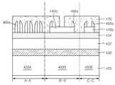
도 4a 및 도 4b 내지 도 14a 및 도 14b는 본 발명의 바람직한 실시예에 따른 반도체 소자의 미세 패턴 형성 방법을 설명하기 위하여 공정 순서에 따라 도시한 도면들이다. 특히, 도 4a 내지 도 14a는 각각 도 3의 "IV" 로 표시된 장방형 부분의 평면도이고, 도 4b 내지 도 14b는 각각 도 3의 "IV" 로 표시된 장방형 부분 중에서 A - A' 선, B - B' 선, 및 C - C' 선에 따르는 단면들에 대응되는 각 부분의 단면도이다.FIGS. 4A and 4B to FIGS. 14A and 14B are views illustrating a method of forming a fine pattern of a semiconductor device according to a preferred embodiment of the present invention in order of process. In particular, Figs. 4A to 14A are respectively a plan view of a rectangular portion denoted by "IV" in Fig. 3 and Figs. 4B to 14B are cross- Line, and C-C ', respectively.
도 4a 및 도 4b를 참조하면, 먼저 메모리 셀 영역(300A)과, 접속 영역(300B)과, 주변회로 영역(300C) (도 3 참조)을 가지는 기판(400)을 준비한다. 상기 기판(400)은 실리콘 기판으로 이루어질 수 있다.4A and 4B, a
상기 기판(400) 위에 상기 도전 라인들을 형성하는 데 필요한 도전층(430)을 형성하고, 상기 도전층(430) 위에 제1 하드마스크층(432) 및 제2 하드마스크층(434)을 차례로 형성한다. 경우에 따라, 상기 제1 하드마스크층(432) 및 제2 하드마스크층(434)중 어느 하나는 생략될 수 있다. 또는, 상기 제1 하드마스크층(432) 및 제2 하드마스크층(434) 외에 다른 하드마스크층(도시 생략)을 더 형성 하여, 상기 제1 하드마스크층(432) 및 제2 하드마스크층(434)을 포함하는 3 층 이상의 하드마스크 적층 구조를 형성할 수도 있다.A
그 후, 상기 제2 하드마스크층(434) 위에 제3 하드마스크층(440)을 형성한다. 상기 제3 하드마스크층(440)은 후속 공정에서 메모리 셀 영역(300A)에 형성되는 복수의 도전 라인(301, 302, ..., 332) (도 3 참조)에 비해 큰 사이즈 또는 콘 폭을 가지는 패턴들, 또는 상기 복수의 도전 라인(301, 302, ..., 332) (도 3 참조)이 형성되는 영역에 비해 낮은 밀도로 형성되는 패턴들을 형성하기 위한 식각 마스크로 사용하기 위한 것이다.A
도 4a 및 도 4b에서, 상기 도전층(430)으로부터 워드 라인을 형성하는 경우, 상기 도전층(430)은 TaN, TiN, W, WN, HfN 및 텅스텐 실리사이드로 이루어지는 군에서 선택되는 어느 하나, 또는 이들의 조합으로 이루어지는 도전 물질을 포함할 수 있다. 또는, 상기 도전층(430)으로부터 비트 라인을 형성하는 경우, 상기 도전층(430)은 도핑된 폴리실리콘 또는 금속으로 이루어질 수 있다.4A and 4B, when a word line is formed from the
상기 제1 하드마스크층(432) 및 제2 하드마스크층(434)은 서로 다른 식각 특성을 가지는 물질로 이루어질 수 있다. 예를 들면, 상기 제1 하드마스크층(432)은 산화막으로 이루어지고, 상기 제2 하드마스크층(434)은 폴리실리콘막 또는 질화막으로 이루어질 수 있다. 상기 제1 하드마스크층(432)은 약 1000 ∼ 3000 Å의 두께로 형성될 수 있다. 상기 제2 하드마스크층(434)은 약 300 ∼ 1000 Å의 두께로 형성될 수 있다.The first
상기 제3 하드마스크층(440)은 상기 제1 하드마스크층(432)과 동일 또는 유 사한 식각 특성을 가지는 물질로 이루어질 수 있다. 예를 들면, 상기 제3 하드마스크층(440)은 산화막으로 이루어질 수 있다.The third
도 5a 및 도 5b를 참조하면, 상기 제3 하드마스크층(440) 중 상기 기판(400)의 제1 영역(400A)을 덮고 있는 부분을 제거하여, 상기 제1 영역(400A)에서 상기 제2 하드마스크층(434)을 노출시키는 제3 하드마스크 패턴(440a)을 형성한다.Referring to FIGS. 5A and 5B, a portion of the third
상기 기판(400)의 제1 영역(400A)은 메모리 셀 영역(300A) 및 접속 영역(300B) 중 더블 패터닝 (double patterning) 공정에 의해 패턴 밀도를 배가(倍加)시켜 협폭(narrow width)의 미세 패턴을 형성하게 될 영역이다. 상기 기판(400)의 제1 영역(400A)은 도 3에 예시된 도전 라인(301, 302, ..., 332)이 형성되는 영역에 대응된다.The
상기 기판(400)의 제1 영역(400A)에서 상기 제3 하드마스크층(440)이 제거됨으로써 상기 제1 영역(400A)에서는 상기 제2 하드마스크층(434)이 노출된다. 상기 기판(400)의 제2 영역(400B)은 상기 제3 하드마스크 패턴(440a)으로 덮여 있다. 상기 기판(400)의 제2 영역(400B)은 상기 제1 영역(400A)에 비해 큰 사이즈 또는 큰 폭을 가지는 광폭(wide width)의 패턴들, 또는 비교적 낮은 밀도로 형성되는 패턴들이 형성될 영역이다.The third
도 6a 및 도 6b를 참조하면, 상기 기판(400)의 제1 영역(400A) 및 제2 영역(400B)에서 각각 상기 제2 하드마스크층(434) 및 제3 하드마스크 패턴(440a) 위에 복수의 몰드 마스크 패턴(450)을 형성한다. 상기 복수의 몰드 마스크 패턴(450)은 각각 메모리 셀 영역(300A) 및 접속 영역(300B)에서 상기 제2 하드마스크 층(434)의 상면 및 상기 제3 하드마스크 패턴(440a)의 상면에 걸쳐서 연장되도록 형성될 수 있다. 이 때, 1 개의 몰드 마스크 패턴(450)은 제1 영역(400A)에 형성되는 협폭 몰드 마스크 패턴(450s)과 제2 영역(400B)에 형성되는 광폭 몰드 마스크 패턴(450w)이 상호 연결되어 있는 구조를 가진다. 또는, 메모리 셀 영역(300A)에서 도 3에 예시된 스트링 선택 라인(SSL) 및 접지 선택 라인(GSL)을 형성하거나 주변회로 영역(300C)에서 주변회로용 도전 패턴(372)을 형성하기 위하여, 상기 몰드 마스크 패턴(450)이 상기 제3 하드마스크 패턴(440a)의 상면에만 연장되도록 형성될 수도 있다.Referring to FIGS. 6A and 6B, a plurality of first hard mask layers 434 and a plurality of second
상기 복수의 몰드 마스크 패턴(450)은 상기 제2 하드마스크층(434) 및 제3 하드마스크 패턴(440a) 각각에 대하여 식각 선택비를 가지는 물질로 이루어진다. 예를 들면, 상기 복수의 몰드 마스크 패턴(450)은 탄소 함유막 또는 폴리실리콘막으로 이루어질 수 있다. 특정한 예로서, 상기 제2 하드마스크층(434)이 폴리실리콘막으로 이루어지고 상기 제3 하드마스크 패턴(440a)이 산화막으로 이루어진 경우, 상기 복수의 몰드 마스크 패턴(450)은 탄소 함유막으로 이루어질 수 있다. 다른 예로서, 상기 제2 하드마스크층(434)이 질화막으로 이루어지고 상기 제3 하드마스크 패턴(440a)이 산화막으로 이루어진 경우, 상기 복수의 몰드 마스크 패턴(450)은 폴리실리콘막으로 이루어질 수 있다.The plurality of
상기 복수의 몰드 마스크 패턴(450)을 형성하는 데 있어서, 상기 기판(400)의 제1 영역(400A) 및 제2 영역(400B)에서 상기 기판(400) 상면으로부터 상기 복수의 몰드 마스크 패턴(450) 각각의 상면까지의 거리(D1, D2)가 균일하게 되도록 형 성하는 것이 바람직하다.The plurality of
상기 복수의 몰드 마스크 패턴(450)을 형성하기 위하여, 먼저 상기 제2 하드마스크층(434) 및 제3 하드마스크 패턴(440a) 위에 스핀 코팅 (spin coating) 또는 CVD (chemical vapor deposition) 공정을 이용하여 평탄화된 상면을 가지는 몰드 마스크층을 형성한 후, 포토레지스트 패턴(도시 생략)을 식각 마스크로 이용하여 상기 몰드 마스크층을 식각하여 도 6a 및 도 6b에 예시된 복수의 몰드 마스크 패턴(450) 형상으로 패터닝할 수 있다.In order to form the plurality of
예를 들면, 상기 복수의 몰드 마스크 패턴(450)을 탄소함유막으로 형성하기 위하여, 상기 제2 하드마스크층(434) 및 제3 하드마스크 패턴(440a) 위에 유기 화합물을 약 1000 ∼ 5000 Å의 두께로 스핀 코팅하여 유기 화합물층을 형성한다. 상기 유기 화합물은 페닐, 벤젠, 또는 나프탈렌과 같은 방향족 환을 포함하는 방향족 환을 포함하는 탄화수소 화합물 또는 그 유도체로 이루어질 수 있다. 상기 유기 화합물은 그 총 중량을 기준으로 약 85 ∼ 99 중량%의 비교적 높은 탄소 함량을 가지는 물질로 이루어질 수 있다. 상기 유기화합물층을 약 150 ∼ 350 ℃의 온도하에서 1차 베이크(bake)하여 탄소함유막을 형성할 수 있다. 상기 1차 베이크는 약 60 초 동안 행해질 수 있다. 그 후, 상기 탄소함유막을 약 300 ∼ 550 ℃의 온도하에서 2차 베이크하여 경화시킨다. 상기 2차 베이크는 약 30 ∼ 300 초 동안 행해질 수 있다. 이와 같이, 상기 탄소함유막을 2차 베이크 공정에 의해 경화시킴으로써 상기 탄소함유막 위에 다른 막질을 형성할 때 약 400 ℃ 이상의 비교적 고온하에서 증착 공정을 행하여도 증착 공정 중에 상기 탄소함유막에 악영향이 미치지 않게 된다.For example, in order to form the plurality of
도 7a 및 도 7b를 참조하면, 상기 복수의 몰드 마스크 패턴(450)이 형성된 결과물상에 상기 몰드 마스크 패턴(450)의 상면 및 측벽을 균일한 두께로 덮는 스페이서 마스크층(460)을 형성한다. 상기 스페이서 마스크층(460)이 형성된 후, 상기 복수의 몰드 마스크 패턴(450) 사이로 노출되는 상기 제2 하드마스크층(434) 및 제3 하드마스크 패턴(440a)의 상면도 상기 스페이서 마스크층(460)에 의해 균일한 두께로 덮이게 된다.Referring to FIGS. 7A and 7B, a
상기 스페이서 마스크층(460)은 상기 제3 하드마스크 패턴(440a)과 동일 또는 유사한 식각 특성을 가지는 물질로 이루어질 수 있다. 예를 들면, 상기 스페이서 마스크층(460)은 산화막으로 이루어질 수 있다. 상기 기판(400)상에서 상기 스페이서 마스크층(460)을 균일한 두께로 형성되도록 하기 위하여 ALD (atomic layer deposition) 공정을 이용할 수 있다.The
도 8a 및 도 8b를 참조하면, 상기 스페이서 마스크층(460)을 에치백하여, 복수의 몰드 마스크 패턴(450) 각각의 측벽들을 덮는 루프(loop) 형상의 복수의 스페이서(460a)를 형성한다. 이 때, 상기 기판(400)의 제1 영역(400A)에서는, 상기 제2 하드마스크층(434)이 노출될 때 까지 상기 스페이서 마스크층(460)이 에치백되어 상기 몰드 마스크 패턴(450)의 측벽들을 덮는 복수의 스페이서(460a)가 형성된다. 반면, 상기 기판(400)의 제2 영역(400B)에서는, 상기 스페이서 마스크층(460)이 에치백됨에 따라 상기 제1 영역(400A)에서 상기 제2 하드마스크층(434)이 노출되기 전에 상기 제3 하드마스크 패턴(440a)이 먼저 노출된다. 상기 제3 하드마스크 패턴(440a)과 상기 스페이서 마스크층(460)은 상호 동일 또는 유사한 막질로 이루어 지므로, 상기 제2 영역(400B)에서 상기 제3 하드마스크 패턴(440a)이 노출된 후 상기 제1 영역(400A)에서 상기 제2 하드마스크층(434)이 노출될 때까지 상기 스페이서 마스크층(460)이 계속 에치백되는 동안 제2 영역(400B)에서는 상기 복수의 스페이서(460a)의 형성 후 노출된 제3 하드마스크 패턴(440a)이 에치백되어 상기 제3 하드마스크 패턴(440a) 아래에 있던 제2 하드마스크층(434)이 노출된다. 그 결과, 상기 기판(400)의 제2 영역(400B)에서는 상기 몰드 마스크 패턴(450)과 그 양 측벽을 덮고 있는 스페이서(460a)의 각각의 폭의 합에 대응되는 폭을 가지는 저밀도 패턴 형성용 제3 하드마스크 패턴(440b)이 얻어진다.8A and 8B, the
도 9a 및 도 9b를 참조하면, 상기 복수의 스페이서(460a), 저밀도 패턴 형성용 제3 하드마스크 패턴(440b), 및 제2 하드마스크층(434)의 식각이 억제되는 조건하에서 상기 기판(400)의 제1 영역(400A) 및 제2 영역(400B)으로부터 상기 복수의 몰드 마스크 패턴(450)을 완전히 제거한다.9A and 9B, under the condition that the etching of the plurality of spacers 460a, the third
그 결과, 상기 기판(400)의 제1 영역(400A)에는 상기 제2 하드마스크층(434) 위에 복수의 스페이서(460a) 만 남게 되고, 제2 영역(400B)에는 상기 제2 하드마스크층(434) 위에 저밀도 패턴 형성용 제3 하드마스크 패턴(440b)과 상기 저밀도 패턴 형성용 제3 하드마스크 패턴(440b)의 일부를 덮고 있는 복수의 스페이서(460a)가 남게 된다.As a result, only a plurality of
도 10a 및 도 10b를 참조하면, 상기 복수의 스페이서(460a), 저밀도 패턴 형성용 제3 하드마스크 패턴(440b), 및 제2 하드마스크층(434) 위에 분리용 마스크 패턴(470)을 형성한다.10A and 10B, a
상기 분리용 마스크 패턴(470)이 형성된 후, 상기 기판(400) 상의 접속 영역(300B) (도 3 참조)에서 상기 복수의 스페이서(460a)의 일부와 상기 저밀도 패턴 형성용 제3 하드마스크 패턴(440b)의 일부가 상기 분리용 마스크 패턴(470)을 통해 외부로 노출된다. 상기 분리용 마스크 패턴(470)이 형성된 후, 상기 기판(400)의 메모리 셀 영역(300A) 및 주변회로 영역(300C) (도 3 참조)에서는 상기 스페이서(460a) 및 저밀도 패턴 형성용 제3 하드마스크 패턴(440b)이 상기 분리용 마스크 패턴(470)에 의해 완전히 덮여 외부로 노출되지 않는다.After the
상기 분리용 마스크 패턴(470)은 포토레지스트 패턴으로 이루어질 수 있다.The
도 11a 및 도 11b를 참조하면, 상기 분리용 마스크 패턴(470)을 식각 마스크로 하여 상기 접속 영역(300B)에서 복수의 스페이서(460a) 및 저밀도 패턴 형성용 제3 하드마스크 패턴(440b)의 노출된 부분들을 제거하는 트리밍(trimming) 공정을 행하여, 상기 기판(400)의 메모리 셀 영역(300A) 및 주변회로 영역(300C)에서 복수의 몰드 마스크 패턴(450) 주위에 형성되었던 루프 형상의 스페이서(460a)를 각각 2 개로 분리시키는 동시에, 접속 영역(300B)에 있는 저밀도 패턴 형성용 제3 하드마스크 패턴(440b)을 각각 2 개로 분리시켜 콘택 패드용 제3 하드마스크 패턴(440c)을 형성한다.11A and 11B, the plurality of spacers 460a and the third hard mask pattern for low
그 후, 상기 분리용 마스크 패턴(470)을 제거한다.Thereafter, the
도 12a 및 도 12b를 참조하면, 상기 기판(400)의 제1 영역(400A)에서는 상기 복수의 스페이서(460a)를 식각 마스크로 이용하고, 제2 영역(400B)에서는 상기 저밀도 패턴 형성용 제3 하드마스크 패턴(440b) 및 콘택 패드용 제3 하드마스크 패 턴(440c)을 각각 식각 마스크로 이용하여 상기 제2 하드마스크층(434)을 식각하여, 상기 제1 하드마스크층(432)을 노출시키는 복수의 제2 하드마스크 패턴(434a)을 형성한다.Referring to FIGS. 12A and 12B, the plurality of
상기 복수의 제2 하드마스크 패턴(434a)이 형성된 후, 상기 제2 하드마스크 패턴(434a)의 상면에는 도 12b에 도시한 바와 같이 상기 복수의 스페이서(460a)와, 저밀도 패턴 형성용 제3 하드마스크 패턴(440b) 및 콘택 패드용 제3 하드마스크 패턴(440c)이 잔류할 수 있다. 도 12a에서, 상기 제2 하드마스크 패턴(434a)의 상면에 잔류하는 다른 막들의 도시는 생략하였다.After the plurality of second
도 13a 및 도 13b를 참조하면, 상기 기판(400)의 제1 영역(400A) 및 제2 영역(400B)에서 상기 제2 하드마스크 패턴(434a)을 식각 마스크로 이용하여 상기 제1 하드마스크층(432)을 식각하여, 상기 도전층(430)을 노출시키는 복수의 제1 하드마스크 패턴(432a)을 형성한다.Referring to FIGS. 13A and 13B, the first
상기 복수의 제1 하드마스크 패턴(432a)이 형성된 후, 상기 제1 하드마스크 패턴(432a)의 상면에는 도 13b에 도시한 바와 같이 상기 제2 마스크 패턴(434a)이 잔류할 수 있다. 도 13a에서, 상기 제1 하드마스크 패턴(432a)의 상면에 잔류하는 다른 막들의 도시는 생략하였다.After the plurality of first
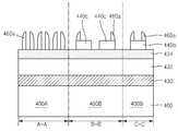
도 14a 및 도 14b를 참조하면, 상기 기판(400)의 제1 영역(400A) 및 제2 영역(400B)에서 상기 제1 하드마스크 패턴(432a)을 식각 마스크로 이용하여 상기 도전층(430)을 식각한다.Referring to FIGS. 14A and 14B, the first
그 결과, 상기 기판(400)의 제1 영역(400A)에는 상기 복수의 스페이서(460a) 의 폭 및 피치가 전사된 복수의 제1 도전 패턴(430a)이 형성된다. 그리고, 상기 기판의 제2 영역(400B)에는 상기 저밀도 패턴 형성용 제3 하드마스크 패턴(440b) 및 콘택 패드용 제3 하드마스크 패턴(440c)의 폭 및 피치가 전사된 제2 도전 패턴(430b) 및 제3 도전 패턴(430c)이 형성된다. 상기 제3 도전 패턴(430c)은 상기 제1 도전 패턴(430a)과 일체로 형성된다. 상기 제1 도전 패턴(430a)은 제1 영역(400A)에서 상기 협폭 몰드 마스크 패턴(450s) (도 6a 및 도 6b 참조)으로부터 그 패턴 밀도가 배가된 스페이서(460a)의 폭이 그대로 전사되어 협폭의 도전 패턴으로 형성된다. 그리소, 상기 제1 도전 패턴(430c)은 제2 영역(400B)에서 상기 광폭 몰드 마스크 패턴(450w) (도 6a 및 도 6b 참조)으로부터 유도되는 비교적 광폭의 저밀도 패턴 형성용 제3 하드마스크 패턴(440b)의 폭이 전사되어 광폭의 도전 패턴으로 형성된다.As a result, a plurality of first
상기 복수의 제1 도전 패턴(430a)은 도 3에 예시된 메모리 셀 영역(300A)에서 복수의 도전 라인(301, 302, ..., 332)에 대응하고, 상기 제2 도전 패턴(430b)은 도 3에 예시된 메모리 셀 영역(300A)에서 스트링 선택 라인(SSL) 및 접지 선택 라인(GSL)에 대응한다. 그리고, 상기 제3 도전 패턴(430c)은 도 3에 예시된 접속 영역(300B)에서 상기 복수의 도전 라인(301, 302, ..., 332)과 각각 일체로 형성되는 복수의 콘택 패드(352)에 대응한다.The plurality of first
상기한 바와 같이, 상기 복수의 제1 도전 패턴(430a), 제2 도전 패턴(430b) 및 제3 도전 패턴(430c)은 각각 1 회의 포토리소그래피 공정에 의해 기판(400)의 제1 영역(400A)및 제2 영역(400B)에서 각각 동시에 형성되는 복수의 몰드 마스크 패턴(450)을 이용하여 얻어진다. 즉, 제1 영역(400A)에서는 상기 복수의 몰드 마스크 패턴(450) 중 협폭 몰드 마스크 패턴(450s)으로부터 패턴 밀도가 배가(倍加)된 복수의 스페이서(460a)를 전사하는 공정을 통해 상기 제1 도전 패턴(430a)이 얻어지고, 제2 영역(400B)에서는 상기 복수의 몰드 마스크 패턴(450) 중 광폭 몰드 마스크 패턴(450w) 및 그 측벽에 형성되는 스페이서(460a)를 동시에 전사하는 공정을 통해 상기 제2 도전 패턴(430b) 및 제3 도전 패턴(430c)이 얻어진다.As described above, the first
이와 같이, 메모리 셀 영역(300A)을 구성하는 복수의 도전 라인(301, 302, ..., 332)을 형성하는 데 필요한 포토리소그래피 공정과, 이들을 주변 회로에 연결시키기 위한 복수의 콘택 패드(352), 메모리 셀 영역(300A)에 형성되는 스트링 선택 라인(SSL) 및 접지 선택 라인(GSL), 및 주변회로 영역(300C)에 형성되는 주변회로용 도전 패턴(372)과 같은 비교적 큰 패턴들을 형성하기 위한 포토리소그래피 공정을 별도의 공정으로 행하지 않고 1 회의 포토리소그래피 공정을 통해 동시에 형성함으로써 이들 사이에 발생될 수 있는 미스얼라인 문제를 근본적으로 해결할 수 있다.As described above, the photolithography process necessary for forming the plurality of
또한, 기판(400)의 제1 영역(400A) 및 제2 영역(400B)에서 상기 복수의 제1 도전 패턴(430a), 제2 도전 패턴(430b) 및 제3 도전 패턴(430c)을 형성하기 위한 식각 공정시, 1 회의 포토리소그래피 공정을 통해 얻어지는 식각 마스크를 이용하여 식각 공정을 동시에 행하므로, 동일 또는 유사한 식각 특성을 가지는 물질을 식각 마스크로 이용할 수 있다. 따라서, 서로 다른 패턴 밀도를 가지는 다양한 형상의 패턴을 동시에 형성하는 데 있어서, 식각 마스크의 재료 차이에 따른 식각 특성 및 패턴 균일도의 열화 가능성을 배제할 수 있다.The plurality of first
위에서 도 4a 및 도 4b 내지 도 14a 및 도 14b를 참조하여 설명한 실시예에서는 기판(400)상에 형성된 도전층(430)을 식각하여 제1 도전 패턴(430a), 제2 도전 패턴(430b) 및 제3 도전 패턴(430c)을 형성하는 공정을 예로 들어 설명하였으나, 본 발명은 이에 한정되는 것은 아니다. 예를 들면, 본 발명에 따른 반도체 소자의 미세 패턴 형성 방법은 상기 기판(400)에 활성 영역을 정의하는 데 이용될 수도 있다. 도시하지는 않았으나, 본 발명에 따른 반도체 소자의 미세 패턴 형성 방법에 따라 상기 기판(400)에 활성 영역을 정의하기 위하여, 상기 기판(400) 위에 상기 도전층(430)을 형성하는 공정을 생략하고, 상기 기판(400)의 바로 위에 패드 산화막 및 제1 하드마스크층(432)을 차례로 형성한 후, 도 4a 및 도 4b 내지 도 13a 및 도 13b의 공정을 거쳐 얻어진 제1 하드마스크 패턴(432a)을 형성하는 공정까지 진행한 후, 상기 제1 하드마스크 패턴(432a)을 식각 마스크로 이용하여 상기 기판(400)을 식각하여 상기 기판(400)에 다양한 폭을 가지는 복수의 트렌치(trench)를 형성하고, 상기 복수의 트렌치 내에 절연 물질을 매립하여 소자분리막을 형성할 수 있다.The
이상, 본 발명을 바람직한 실시예를 들어 상세하게 설명하였으나, 본 발명은 상기 실시예에 한정되지 않고, 본 발명의 기술적 사상 및 범위 내에서 당 분야에서 통상의 지식을 가진 자에 의하여 여러가지 변형 및 변경이 가능하다.While the present invention has been particularly shown and described with reference to exemplary embodiments thereof, it is to be understood that the invention is not limited to the disclosed exemplary embodiments, but, on the contrary, This is possible.
도 1은 통상의 NAND 플래시 메모리 소자의 메모리 셀 어레이와, 그 주변 회로들을 나타낸 블록 다이어그램이다.1 is a block diagram showing a memory cell array of a conventional NAND flash memory device and peripheral circuits thereof.
도 2는 통상의 NAND 플래시 메모리 소자의 메모리 셀 어레이의 구조를 설명하기 위한 회로도이다.2 is a circuit diagram for explaining a structure of a memory cell array of a conventional NAND flash memory device.
도 3은 본 발명의 바람직한 실시예에 따른 반도체 소자의 미세 패턴 형성 방법에 따라 구현될 수 있는 반도체 소자의 일부 구성을 예시한 평면도이다.3 is a plan view illustrating a partial structure of a semiconductor device that can be implemented according to a method of forming a fine pattern of a semiconductor device according to a preferred embodiment of the present invention.
도 4a 및 도 4b 내지 도 14a 및 도 14b는 본 발명의 바람직한 실시예에 따른 반도체 소자의 미세 패턴 형성 방법을 설명하기 위하여 공정 순서에 따라 도시한 도면들로서, 도 4a 내지 도 14a는 각각 도 3의 "IV" 로 표시된 장방형 부분의 평면도이고, 도 4b 내지 도 14b는 각각 도 3의 "IV" 로 표시된 장방형 부분 중에서 A - A' 선, B - B' 선, 및 C - C' 선에 따르는 단면들에 대응되는 각 부분의 단면도이다.FIGS. 4A and 4B are cross-sectional views illustrating a method of forming a fine pattern of a semiconductor device according to a preferred embodiment of the present invention. FIGS. 4A through 14A are cross- 4B to 14B are plan views of a rectangular portion indicated by "IV", and FIGS. 4B to 14B are cross-sectional views taken along line A-A ', line B-B', and line C-C ' Fig. 3 is a cross-sectional view of each part corresponding to Fig.
<도면의 주요 부분에 대한 부호의 설명>Description of the Related Art
300A: 메모리 셀 영역, 300B: 접속 영역, 300C: 주변회로 영역, 301, 302, ..., 332: 도전 라인, 340: 메모리 셀 블록, 352: 콘택 패드, 372: 주변회로용 도전 패턴, 400: 기판, 400A: 제1 영역, 400B: 제2 영역, 430: 도전층, 430a: 제1 도전 패턴, 430b: 제2 도전 패턴, 430c: 제3 도전 패턴, 432: 제1 하드마스크층, 432a: 제1 하드마스크 패턴, 434: 제2 하드마스크층, 434a: 제2 하드마스크 패턴, 440: 제3 하드마스크층, 440a: 제3 하드마스크 패턴, 440b: 저밀도 패턴 형성용 제 3 하드마스크 패턴, 440c: 콘택 패드용 제3 하드마스크 패턴, 450: 몰드 마스크 패턴, 450s: 협폭 몰드 마스크 패턴, 450w: 광폭 몰드 마스크 패턴, 460: 스페이서 마스크층, 460a: 스페이서, 470: 분리용 마스크 패턴,A plurality of memory cells each having a plurality of memory cells each including a plurality of memory cells and a plurality of memory cells each having a plurality of memory cells, The first
Claims (35)
Translated fromKoreanPriority Applications (6)
| Application Number | Priority Date | Filing Date | Title |
|---|---|---|---|
| KR1020080057020AKR101468028B1 (en) | 2008-06-17 | 2008-06-17 | Method for forming fine pattern of semiconductor device |
| US12/290,420US8057692B2 (en) | 2008-06-17 | 2008-10-30 | Methods of forming fine patterns in the fabrication of semiconductor devices |
| CN2009101458849ACN101609814B (en) | 2008-06-17 | 2009-06-17 | Method of forming semiconductor device and storage system |
| JP2009144204AJP5303374B2 (en) | 2008-06-17 | 2009-06-17 | Method for forming semiconductor device and method for manufacturing memory system |
| US12/639,542US8686563B2 (en) | 2008-06-17 | 2009-12-16 | Methods of forming fine patterns in the fabrication of semiconductor devices |
| US14/186,617US9093454B2 (en) | 2008-06-17 | 2014-02-21 | Semiconductor devices having fine patterns |
Applications Claiming Priority (1)
| Application Number | Priority Date | Filing Date | Title |
|---|---|---|---|
| KR1020080057020AKR101468028B1 (en) | 2008-06-17 | 2008-06-17 | Method for forming fine pattern of semiconductor device |
Publications (2)
| Publication Number | Publication Date |
|---|---|
| KR20090131173A KR20090131173A (en) | 2009-12-28 |
| KR101468028B1true KR101468028B1 (en) | 2014-12-02 |
Family
ID=41415180
Family Applications (1)
| Application Number | Title | Priority Date | Filing Date |
|---|---|---|---|
| KR1020080057020AActiveKR101468028B1 (en) | 2008-06-17 | 2008-06-17 | Method for forming fine pattern of semiconductor device |
Country Status (4)
| Country | Link |
|---|---|
| US (3) | US8057692B2 (en) |
| JP (1) | JP5303374B2 (en) |
| KR (1) | KR101468028B1 (en) |
| CN (1) | CN101609814B (en) |
Families Citing this family (31)
| Publication number | Priority date | Publication date | Assignee | Title |
|---|---|---|---|---|
| KR101435520B1 (en) | 2008-08-11 | 2014-09-01 | 삼성전자주식회사 | Semiconductor device and pattern forming method of semiconductor device |
| KR101532012B1 (en)* | 2008-12-24 | 2015-06-30 | 삼성전자주식회사 | Semiconductor device and method of forming patterns for semiconductor device |
| JP5322668B2 (en)* | 2009-01-21 | 2013-10-23 | 株式会社東芝 | Semiconductor device manufacturing method and photomask |
| KR101016826B1 (en)* | 2009-02-13 | 2011-02-21 | 주식회사 하이닉스반도체 | Pattern of Semiconductor Device and Formation Method thereof |
| KR101093969B1 (en) | 2010-08-04 | 2011-12-15 | 주식회사 하이닉스반도체 | Fine pattern formation method |
| KR101927924B1 (en)* | 2011-10-28 | 2018-12-12 | 삼성전자주식회사 | Semiconductor device and method for forming patterns of semiconductor device |
| CN102522371B (en)* | 2011-12-22 | 2016-06-08 | 上海华虹宏力半导体制造有限公司 | The manufacture method of contact hole |
| JP5881569B2 (en)* | 2012-08-29 | 2016-03-09 | 株式会社東芝 | Pattern formation method |
| KR20140064458A (en) | 2012-11-20 | 2014-05-28 | 삼성전자주식회사 | Method of forming semiconductor device and the device |
| US9378979B2 (en) | 2012-11-20 | 2016-06-28 | Samsung Electronics Co., Ltd. | Methods of fabricating semiconductor devices and devices fabricated thereby |
| CN103839769B (en)* | 2012-11-20 | 2016-12-21 | 华邦电子股份有限公司 | pattern forming method |
| US8987142B2 (en)* | 2013-01-09 | 2015-03-24 | Taiwan Semiconductor Manufacturing Co., Ltd. | Multi-patterning method and device formed by the method |
| CN104425225A (en)* | 2013-09-04 | 2015-03-18 | 中芯国际集成电路制造(上海)有限公司 | Forming method for triple graphs |
| US9368348B2 (en) | 2013-10-01 | 2016-06-14 | Taiwan Semiconductor Manufacturing Company, Ltd. | Self-aligned patterning process |
| KR102223035B1 (en)* | 2014-03-05 | 2021-03-04 | 삼성전자주식회사 | Method of forming patterns for semiconductor device |
| US10163652B2 (en) | 2014-03-13 | 2018-12-25 | Taiwan Semiconductor Manufacturing Company, Ltd. | Mechanisms for forming patterns using multiple lithography processes |
| KR102270752B1 (en)* | 2014-08-11 | 2021-07-01 | 삼성전자주식회사 | Method for forming fine patterns of semiconductor device |
| US9224744B1 (en)* | 2014-09-03 | 2015-12-29 | Sandisk Technologies Inc. | Wide and narrow patterning using common process |
| CN104576400A (en)* | 2015-01-21 | 2015-04-29 | 上海集成电路研发中心有限公司 | Technology integration method of fin field-effect transistor |
| KR102323251B1 (en) | 2015-01-21 | 2021-11-09 | 삼성전자주식회사 | Semiconductor device and method for manufacturing semiconductor device |
| KR102420150B1 (en) | 2015-08-19 | 2022-07-13 | 삼성전자주식회사 | Method of fabricating semiconductor device |
| US9911693B2 (en)* | 2015-08-28 | 2018-03-06 | Micron Technology, Inc. | Semiconductor devices including conductive lines and methods of forming the semiconductor devices |
| KR102410139B1 (en)* | 2015-09-04 | 2022-06-16 | 삼성전자주식회사 | Method for fabricating semiconductor device |
| US9583356B1 (en)* | 2015-09-30 | 2017-02-28 | Taiwan Semiconductor Manufacturing Co., Ltd. | Method for forming semiconductor device structure |
| WO2018165815A1 (en)* | 2017-03-13 | 2018-09-20 | 深圳修远电子科技有限公司 | Chip fanning out method |
| US9905424B1 (en)* | 2017-04-24 | 2018-02-27 | Globalfoundries Inc. | Self-aligned non-mandrel cut formation for tone inversion |
| JP6913569B2 (en)* | 2017-08-25 | 2021-08-04 | 東京エレクトロン株式会社 | How to process the object to be processed |
| CN109994464B (en)* | 2017-12-29 | 2021-04-09 | 长鑫存储技术有限公司 | Layout figure with double spacing and method of forming the same |
| US10276434B1 (en)* | 2018-01-02 | 2019-04-30 | International Business Machines Corporation | Structure and method using metal spacer for insertion of variable wide line implantation in SADP/SAQP integration |
| CN114496931B (en)* | 2020-11-13 | 2024-09-17 | 长鑫存储技术有限公司 | Semiconductor structure and forming method thereof |
| KR20230163051A (en)* | 2022-05-23 | 2023-11-30 | 삼성전자주식회사 | Mathod for manufacturing semiconductor device |
Citations (4)
| Publication number | Priority date | Publication date | Assignee | Title |
|---|---|---|---|---|
| KR20000066340A (en)* | 1999-04-15 | 2000-11-15 | 김영환 | Method for forming a electrode line of a semiconductor device |
| KR20030096563A (en)* | 2002-06-14 | 2003-12-31 | 삼성전자주식회사 | Method Of Forming Fine Pattern Of Semiconductor Device |
| KR20050116421A (en)* | 2004-06-07 | 2005-12-12 | 삼성전자주식회사 | Method of forming self-aligned contact in semiconductor memory device and method of fabricating the semiconductor memory device using the method |
| JP2007305970A (en)* | 2006-04-11 | 2007-11-22 | Toshiba Corp | Method for forming integrated circuit pattern |
Family Cites Families (16)
| Publication number | Priority date | Publication date | Assignee | Title |
|---|---|---|---|---|
| US5138438A (en)* | 1987-06-24 | 1992-08-11 | Akita Electronics Co. Ltd. | Lead connections means for stacked tab packaged IC chips |
| US6034438A (en)* | 1996-10-18 | 2000-03-07 | The Regents Of The University Of California | L-connect routing of die surface pads to the die edge for stacking in a 3D array |
| KR100354440B1 (en) | 2000-12-04 | 2002-09-28 | 삼성전자 주식회사 | Method for forming patterns of semiconductor device |
| US7226853B2 (en)* | 2001-12-26 | 2007-06-05 | Applied Materials, Inc. | Method of forming a dual damascene structure utilizing a three layer hard mask structure |
| US6602779B1 (en)* | 2002-05-13 | 2003-08-05 | Taiwan Semiconductor Manufacturing Co., Ltd | Method for forming low dielectric constant damascene structure while employing carbon doped silicon oxide planarizing stop layer |
| US6689695B1 (en)* | 2002-06-28 | 2004-02-10 | Taiwan Semiconductor Manufacturing Company | Multi-purpose composite mask for dual damascene patterning |
| JP3736639B2 (en)* | 2003-12-12 | 2006-01-18 | セイコーエプソン株式会社 | Semiconductor device, electronic device and manufacturing method thereof |
| JP3722224B2 (en)* | 2003-12-24 | 2005-11-30 | セイコーエプソン株式会社 | Semiconductor chip, semiconductor device, and method of manufacturing semiconductor device |
| US7115525B2 (en) | 2004-09-02 | 2006-10-03 | Micron Technology, Inc. | Method for integrated circuit fabrication using pitch multiplication |
| US7390746B2 (en)* | 2005-03-15 | 2008-06-24 | Micron Technology, Inc. | Multiple deposition for integration of spacers in pitch multiplication process |
| US7253118B2 (en) | 2005-03-15 | 2007-08-07 | Micron Technology, Inc. | Pitch reduced patterns relative to photolithography features |
| JP4127711B2 (en)* | 2006-05-31 | 2008-07-30 | 株式会社東芝 | Semiconductor memory |
| JP4909735B2 (en)* | 2006-06-27 | 2012-04-04 | 株式会社東芝 | Nonvolatile semiconductor memory |
| JP4996155B2 (en) | 2006-07-18 | 2012-08-08 | 株式会社東芝 | Semiconductor device and manufacturing method thereof |
| US7790360B2 (en) | 2007-03-05 | 2010-09-07 | Micron Technology, Inc. | Methods of forming multiple lines |
| JP4638902B2 (en)* | 2007-09-27 | 2011-02-23 | Okiセミコンダクタ株式会社 | Semiconductor device and layout method thereof |
- 2008
- 2008-06-17KRKR1020080057020Apatent/KR101468028B1/enactiveActive
- 2008-10-30USUS12/290,420patent/US8057692B2/enactiveActive
- 2009
- 2009-06-17CNCN2009101458849Apatent/CN101609814B/enactiveActive
- 2009-06-17JPJP2009144204Apatent/JP5303374B2/enactiveActive
- 2009-12-16USUS12/639,542patent/US8686563B2/enactiveActive
- 2014
- 2014-02-21USUS14/186,617patent/US9093454B2/enactiveActive
Patent Citations (4)
| Publication number | Priority date | Publication date | Assignee | Title |
|---|---|---|---|---|
| KR20000066340A (en)* | 1999-04-15 | 2000-11-15 | 김영환 | Method for forming a electrode line of a semiconductor device |
| KR20030096563A (en)* | 2002-06-14 | 2003-12-31 | 삼성전자주식회사 | Method Of Forming Fine Pattern Of Semiconductor Device |
| KR20050116421A (en)* | 2004-06-07 | 2005-12-12 | 삼성전자주식회사 | Method of forming self-aligned contact in semiconductor memory device and method of fabricating the semiconductor memory device using the method |
| JP2007305970A (en)* | 2006-04-11 | 2007-11-22 | Toshiba Corp | Method for forming integrated circuit pattern |
Also Published As
| Publication number | Publication date |
|---|---|
| US20140167290A1 (en) | 2014-06-19 |
| US8057692B2 (en) | 2011-11-15 |
| US9093454B2 (en) | 2015-07-28 |
| CN101609814B (en) | 2013-07-24 |
| US20100090349A1 (en) | 2010-04-15 |
| JP5303374B2 (en) | 2013-10-02 |
| US8686563B2 (en) | 2014-04-01 |
| US20090311861A1 (en) | 2009-12-17 |
| CN101609814A (en) | 2009-12-23 |
| JP2009302546A (en) | 2009-12-24 |
| KR20090131173A (en) | 2009-12-28 |
Similar Documents
| Publication | Publication Date | Title |
|---|---|---|
| KR101468028B1 (en) | Method for forming fine pattern of semiconductor device | |
| US9553082B2 (en) | Process for improving critical dimension uniformity of integrated circuit arrays | |
| KR101566405B1 (en) | Method of forming patterns of semiconductor device | |
| KR101565798B1 (en) | A semiconductor device having an integrated structure of a contact pad and a conductive line | |
| KR101565796B1 (en) | Semiconductor device and pattern forming method of semiconductor device | |
| JP5489500B2 (en) | Method for forming fine pattern of semiconductor element | |
| KR101540083B1 (en) | Method for pattern formation of semiconductor device | |
| KR101085630B1 (en) | Pattern formation method of semiconductor device | |
| KR101618749B1 (en) | Method of forming patterns for semiconductor device | |
| KR101736983B1 (en) | Semiconductor device and method of forming patterns for semiconductor device | |
| KR101515907B1 (en) | Method of forming patterns of semiconductor device | |
| TWI477999B (en) | Method of fabricating a semiconductor device using spacer pattern technology | |
| KR20120001339A (en) | Method of forming fine pattern of semiconductor device | |
| KR101093241B1 (en) | Pattern formation method of semiconductor device | |
| JP2011507308A (en) | Method and related structure for separating a portion of a pitch-multiplied material loop | |
| JP2010535410A (en) | Semiconductor device manufacturing method and semiconductor device obtained thereby | |
| KR20100104861A (en) | Method of forming patterns for semiconductor device | |
| JP2012019184A (en) | Method of forming patterns of semiconductor device | |
| CN113130751A (en) | Manufacturing method of semiconductor structure and semiconductor structure | |
| US8097507B2 (en) | Method of fabricating a semiconductor device | |
| KR101511159B1 (en) | Method for pattern formation of semiconductor device | |
| CN100527381C (en) | Method of manufacturing flash memory device | |
| KR101082719B1 (en) | Pattern formation method of semiconductor device | |
| KR20240145261A (en) | Methods for manufacturing semiconductor devices | |
| KR20100074624A (en) | Flash memory device and method of manufacturing the same |
Legal Events
| Date | Code | Title | Description |
|---|---|---|---|
| PA0109 | Patent application | Patent event code:PA01091R01D Comment text:Patent Application Patent event date:20080617 | |
| PG1501 | Laying open of application | ||
| A201 | Request for examination | ||
| PA0201 | Request for examination | Patent event code:PA02012R01D Patent event date:20130524 Comment text:Request for Examination of Application Patent event code:PA02011R01I Patent event date:20080617 Comment text:Patent Application | |
| E902 | Notification of reason for refusal | ||
| PE0902 | Notice of grounds for rejection | Comment text:Notification of reason for refusal Patent event date:20140418 Patent event code:PE09021S01D | |
| E701 | Decision to grant or registration of patent right | ||
| PE0701 | Decision of registration | Patent event code:PE07011S01D Comment text:Decision to Grant Registration Patent event date:20140902 | |
| GRNT | Written decision to grant | ||
| PR0701 | Registration of establishment | Comment text:Registration of Establishment Patent event date:20141126 Patent event code:PR07011E01D | |
| PR1002 | Payment of registration fee | Payment date:20141127 End annual number:3 Start annual number:1 | |
| PG1601 | Publication of registration | ||
| FPAY | Annual fee payment | Payment date:20181031 Year of fee payment:5 | |
| PR1001 | Payment of annual fee | Payment date:20181031 Start annual number:5 End annual number:5 | |
| FPAY | Annual fee payment | Payment date:20191031 Year of fee payment:6 | |
| PR1001 | Payment of annual fee | Payment date:20191031 Start annual number:6 End annual number:6 | |
| PR1001 | Payment of annual fee | Payment date:20201030 Start annual number:7 End annual number:7 | |
| PR1001 | Payment of annual fee | Payment date:20211027 Start annual number:8 End annual number:8 | |
| PR1001 | Payment of annual fee | Payment date:20231026 Start annual number:10 End annual number:10 |