KR101467509B1 - Image sensor and operating method for image sensor - Google Patents
Image sensor and operating method for image sensorDownload PDFInfo
- Publication number
- KR101467509B1 KR101467509B1KR1020080072992AKR20080072992AKR101467509B1KR 101467509 B1KR101467509 B1KR 101467509B1KR 1020080072992 AKR1020080072992 AKR 1020080072992AKR 20080072992 AKR20080072992 AKR 20080072992AKR 101467509 B1KR101467509 B1KR 101467509B1
- Authority
- KR
- South Korea
- Prior art keywords
- light component
- image sensor
- pixels
- pixel
- charge
- Prior art date
- Legal status (The legal status is an assumption and is not a legal conclusion. Google has not performed a legal analysis and makes no representation as to the accuracy of the status listed.)
- Active
Links
Images


Classifications
- H—ELECTRICITY
- H04—ELECTRIC COMMUNICATION TECHNIQUE
- H04N—PICTORIAL COMMUNICATION, e.g. TELEVISION
- H04N23/00—Cameras or camera modules comprising electronic image sensors; Control thereof
- H04N23/10—Cameras or camera modules comprising electronic image sensors; Control thereof for generating image signals from different wavelengths
- H04N23/12—Cameras or camera modules comprising electronic image sensors; Control thereof for generating image signals from different wavelengths with one sensor only
- H—ELECTRICITY
- H04—ELECTRIC COMMUNICATION TECHNIQUE
- H04N—PICTORIAL COMMUNICATION, e.g. TELEVISION
- H04N25/00—Circuitry of solid-state image sensors [SSIS]; Control thereof
- H04N25/50—Control of the SSIS exposure
- H04N25/57—Control of the dynamic range
- H04N25/58—Control of the dynamic range involving two or more exposures
- H04N25/581—Control of the dynamic range involving two or more exposures acquired simultaneously
- H—ELECTRICITY
- H04—ELECTRIC COMMUNICATION TECHNIQUE
- H04N—PICTORIAL COMMUNICATION, e.g. TELEVISION
- H04N25/00—Circuitry of solid-state image sensors [SSIS]; Control thereof
- H—ELECTRICITY
- H04—ELECTRIC COMMUNICATION TECHNIQUE
- H04N—PICTORIAL COMMUNICATION, e.g. TELEVISION
- H04N25/00—Circuitry of solid-state image sensors [SSIS]; Control thereof
- H04N25/10—Circuitry of solid-state image sensors [SSIS]; Control thereof for transforming different wavelengths into image signals
- H04N25/11—Arrangement of colour filter arrays [CFA]; Filter mosaics
- H04N25/13—Arrangement of colour filter arrays [CFA]; Filter mosaics characterised by the spectral characteristics of the filter elements
- H04N25/131—Arrangement of colour filter arrays [CFA]; Filter mosaics characterised by the spectral characteristics of the filter elements including elements passing infrared wavelengths
- H—ELECTRICITY
- H04—ELECTRIC COMMUNICATION TECHNIQUE
- H04N—PICTORIAL COMMUNICATION, e.g. TELEVISION
- H04N25/00—Circuitry of solid-state image sensors [SSIS]; Control thereof
- H04N25/10—Circuitry of solid-state image sensors [SSIS]; Control thereof for transforming different wavelengths into image signals
- H04N25/11—Arrangement of colour filter arrays [CFA]; Filter mosaics
- H04N25/13—Arrangement of colour filter arrays [CFA]; Filter mosaics characterised by the spectral characteristics of the filter elements
- H04N25/134—Arrangement of colour filter arrays [CFA]; Filter mosaics characterised by the spectral characteristics of the filter elements based on three different wavelength filter elements
- H—ELECTRICITY
- H04—ELECTRIC COMMUNICATION TECHNIQUE
- H04N—PICTORIAL COMMUNICATION, e.g. TELEVISION
- H04N25/00—Circuitry of solid-state image sensors [SSIS]; Control thereof
- H04N25/10—Circuitry of solid-state image sensors [SSIS]; Control thereof for transforming different wavelengths into image signals
- H04N25/11—Arrangement of colour filter arrays [CFA]; Filter mosaics
- H04N25/13—Arrangement of colour filter arrays [CFA]; Filter mosaics characterised by the spectral characteristics of the filter elements
- H04N25/135—Arrangement of colour filter arrays [CFA]; Filter mosaics characterised by the spectral characteristics of the filter elements based on four or more different wavelength filter elements
- H04N25/136—Arrangement of colour filter arrays [CFA]; Filter mosaics characterised by the spectral characteristics of the filter elements based on four or more different wavelength filter elements using complementary colours
- H—ELECTRICITY
- H04—ELECTRIC COMMUNICATION TECHNIQUE
- H04N—PICTORIAL COMMUNICATION, e.g. TELEVISION
- H04N25/00—Circuitry of solid-state image sensors [SSIS]; Control thereof
- H04N25/70—SSIS architectures; Circuits associated therewith
- H04N25/703—SSIS architectures incorporating pixels for producing signals other than image signals
- H04N25/705—Pixels for depth measurement, e.g. RGBZ
- H—ELECTRICITY
- H04—ELECTRIC COMMUNICATION TECHNIQUE
- H04N—PICTORIAL COMMUNICATION, e.g. TELEVISION
- H04N25/00—Circuitry of solid-state image sensors [SSIS]; Control thereof
- H04N25/70—SSIS architectures; Circuits associated therewith
- H04N25/76—Addressed sensors, e.g. MOS or CMOS sensors
- H04N25/77—Pixel circuitry, e.g. memories, A/D converters, pixel amplifiers, shared circuits or shared components
- H04N25/778—Pixel circuitry, e.g. memories, A/D converters, pixel amplifiers, shared circuits or shared components comprising amplifiers shared between a plurality of pixels, i.e. at least one part of the amplifier must be on the sensor array itself
- H—ELECTRICITY
- H04—ELECTRIC COMMUNICATION TECHNIQUE
- H04N—PICTORIAL COMMUNICATION, e.g. TELEVISION
- H04N25/00—Circuitry of solid-state image sensors [SSIS]; Control thereof
- H04N25/70—SSIS architectures; Circuits associated therewith
- H04N25/76—Addressed sensors, e.g. MOS or CMOS sensors
- H04N25/78—Readout circuits for addressed sensors, e.g. output amplifiers or A/D converters
- G—PHYSICS
- G01—MEASURING; TESTING
- G01S—RADIO DIRECTION-FINDING; RADIO NAVIGATION; DETERMINING DISTANCE OR VELOCITY BY USE OF RADIO WAVES; LOCATING OR PRESENCE-DETECTING BY USE OF THE REFLECTION OR RERADIATION OF RADIO WAVES; ANALOGOUS ARRANGEMENTS USING OTHER WAVES
- G01S17/00—Systems using the reflection or reradiation of electromagnetic waves other than radio waves, e.g. lidar systems
- G01S17/88—Lidar systems specially adapted for specific applications
- G01S17/89—Lidar systems specially adapted for specific applications for mapping or imaging
- G01S17/894—3D imaging with simultaneous measurement of time-of-flight at a 2D array of receiver pixels, e.g. time-of-flight cameras or flash lidar
Landscapes
- Engineering & Computer Science (AREA)
- Multimedia (AREA)
- Signal Processing (AREA)
- Physics & Mathematics (AREA)
- Spectroscopy & Molecular Physics (AREA)
- Solid State Image Pick-Up Elements (AREA)
- Transforming Light Signals Into Electric Signals (AREA)
- Length Measuring Devices By Optical Means (AREA)
- Measurement Of Optical Distance (AREA)
- Color Television Image Signal Generators (AREA)
- Optical Radar Systems And Details Thereof (AREA)
Abstract
Translated fromKoreanDescription
Translated fromKorean본 발명은 이미지 센서, 이미징 장치, 이미지 센서의 동작 방법, 및 이미징 방법에 관한 것이다.The present invention relates to an image sensor, an imaging apparatus, an operation method of an image sensor, and an imaging method.
최근 이미지 센서(image sensor)를 구비한 휴대용 장치(예를 들어, 디지털 카메라, 이동 통신 단말기 등)가 개발되어 판매되고 있다. 이미지 센서는 픽셀 (pixel)들 또는 포토사이트 (Photosite)들로 불리는 작은 포토다이오드 (photodiode)들의 어레이(array)로서 구성된다. 일반적으로 픽셀은 빛으로부터 색상을 직접적으로 추출하지 않으며, 넓은 스펙트럼 밴드의 광자(photon)를 전자(electron)로 변환한다. 따라서 이미지 센서의 픽셀은 넓은 스펙트럼 밴드의 빛 중 색상 획득에 필요한 밴드의 빛만을 입력 받을 필요가 있다. 이미지 센서의 픽셀은 칼라 필터(color filter) 등과 결합하여 특정 색상에 대응하는 광자만을 전자로 변환할 수 있다.2. Description of the Related Art Recently, a portable device (e.g., a digital camera, a mobile communication terminal, etc.) having an image sensor has been developed and sold. The image sensor is configured as an array of small photodiodes called pixels or photosites. In general, a pixel does not directly extract color from light, but it converts photons of a broad spectrum band into electrons. Therefore, the pixel of the image sensor needs to receive only the light of the band necessary for color acquisition among the light of the wide spectrum band. The pixels of the image sensor may be combined with a color filter or the like to convert only photons corresponding to a specific color into electrons.
이미지 센서를 이용하여 3차원 영상을 획득하기 위해서는 색상뿐만 아니라 물체와 이미지 센서 간의 거리에 관한 정보를 얻을 필요가 있다. 일반적으로 물체 와 이미지 센서 간의 거리에 관해 재구성된 영상을 해당 분야에서는 depth image 로 표현하기도 한다. 일반적으로 depth image는 가시광선(visible light) 영역 외의 적외선(infrared light)을 이용하여 얻어질 수 있다.In order to acquire a three-dimensional image using an image sensor, it is necessary to acquire not only the color but also the distance between the object and the image sensor. Generally, the reconstructed image about the distance between the object and the image sensor is represented as a depth image in the related field. In general, a depth image can be obtained using an infrared light outside the visible light region.
본 발명의 일 실시예에 따른 이미지 센서는 복수의 픽셀들을 포함하고, 상기 복수의 픽셀들중 적어도 하나의 픽셀로부터 칼라 값 및 깊이 값을 얻을 수 있다.An image sensor according to an embodiment of the present invention includes a plurality of pixels, and can obtain a color value and a depth value from at least one pixel of the plurality of pixels.
본 발명의 일 실시예에 따른 이미징 장치(imaging device)는 광원 및 이미지 센서를 포함하고, 상기 이미지 센서는 복수의 픽셀들을 포함하고 상기 복수의 픽셀들중 적어도 하나의 픽셀로부터 칼라 값 및 깊이 값을 얻을 수 있다.An imaging device according to an embodiment of the present invention includes a light source and an image sensor, wherein the image sensor includes a plurality of pixels and receives a color value and a depth value from at least one of the plurality of pixels Can be obtained.
본 발명의 일 실시예에 따른 이미지 센서(image sensor)는 복수의 픽셀들을 포함하고, 상기 복수의 픽셀들 각각은 광 검출 엘리먼트(light-detector element), 및 가시 광 성분을 상기 광 검출 엘리먼트로 선택적으로 투과시키고, 비가시 광 성분을 상기 광 검출 엘리먼트로 투과시키는 필터를 포함할 수 있다.An image sensor in accordance with an embodiment of the present invention includes a plurality of pixels, each of the plurality of pixels including a light-detecting element, and a light- And a filter that transmits an invisible light component to the photodetecting element.
본 발명의 일 실시예에 따른 이미징 장치(imaging device)는 비가시 광 성분을 생성하는 광원, 및 복수의 픽셀들을 포함하고, 상기 복수의 픽셀들 각각은 광 검출 엘리먼트, 및 가시 광 성분을 상기 광 검출 엘리먼트로 선택적으로 투과시키고, 비가시 광 성분을 상기 광 검출 엘리먼트로 투과시키는 필터를 포함할 수 있다.An imaging device in accordance with an embodiment of the present invention includes a light source that generates an invisible light component and a plurality of pixels, each of the plurality of pixels includes a light detection element, And a filter for selectively transmitting the visible light component to the detection element and transmitting the invisible light component to the photo detection element.
본 발명의 일 실시예에 따른 이미지 센서는 적어도 하나의 픽셀을 포함하고, 상기 적어도 하나의 픽셀은 광 검출 엘리먼트를 부유 확산 노드와 연결하는 제1 전달부, 상기 부유 확산 노드의 전압 및 행 제어 신호에 기초하여 비트 라인의 전압을 제어하는 선택 구동부, 및 상기 광 검출 엘리먼트를 싱크 라인과 연결하는 제2 전달부를 포함할 수 있다.An image sensor according to an embodiment of the present invention includes at least one pixel, wherein the at least one pixel includes a first transmitter for coupling the photo-sensing element to the floating diffusion node, a voltage and row control signal And a second transfer unit for connecting the photodetecting element to the sink line.
본 발명의 일 실시예에 따른 이미지 센서 동작 방법(method of operating image sensor)은 이미지 센서의 픽셀을 이용하여 제1 시간 구간 동안 제1 광 성분을 감지하는 단계 및 상기 이미지 센서의 상기 픽셀을 이용하여 제2 시간 구간 동안 제2 광 성분을 감지하는 단계를 포함할 수 있다.A method of operating an image sensor according to an embodiment of the present invention includes sensing a first light component for a first time period using a pixel of the image sensor and using the pixel of the image sensor And sensing a second light component during a second time interval.
본 발명의 일 실시예에 따른 이미징 방법(imaging method)은 이미지 센서의 복수의 픽셀들을 이용하여 제1 시간 구간 동안 제1 광 성분을 감지하는 단계, 상기 제1 시간 구간 후 제2 광 성분을 조사하는 단계, 상기 이미지 센서의 상기 복수의 픽셀들을 이용하여 상기 제2 광 성분이 물체에 의하여 반사된 반사광을 제2 시간 구간 동안 감지하는 단계, 및 상기 감지된 반사광으로부터 상기 물체의 깊이 영상을 얻는 단계를 포함할 수 있다.An imaging method according to an embodiment of the present invention includes sensing a first light component for a first time period using a plurality of pixels of an image sensor, Detecting the reflected light of the second light component reflected by the object using the plurality of pixels of the image sensor for a second time period and obtaining a depth image of the object from the sensed reflected light, . ≪ / RTI >
본 발명의 일 실시예에 따르면 color에 의해 표현되는 color image 및 distance에 의해 표현되는 depth image를 하나의 픽셀을 이용하여 얻을 수 있는 장치 및 방법을 제공할 수 있다.According to an embodiment of the present invention, it is possible to provide an apparatus and method for obtaining a depth image represented by a color image and a distance represented by color using one pixel.
본 발명의 일 실시예에 따르면 공간 해상도를 줄이지 않고 color image 및 depth image를 하나의 픽셀에 의하여 얻을 수 있다.According to an embodiment of the present invention, a color image and a depth image can be obtained by one pixel without reducing spatial resolution.
본 발명의 일 실시예에 따르면 복수의 픽셀들이 검출 회로를 공유하는 픽셀 구조(pixel structure)를 이용하여 이미지 센서의 크기를 줄일 수 있다.According to an embodiment of the present invention, a pixel structure in which a plurality of pixels share a detection circuit can be used to reduce the size of the image sensor.
본 발명의 일 실시예에 따르면 depth 영상의 신호 대 잡음 비(Signal to Noise Ratio, SNR)를 높일 수 있다.According to an embodiment of the present invention, a signal-to-noise ratio (SNR) of a depth image can be increased.
이하에서, 본 발명에 따른 실시예들을 첨부된 도면을 참조하여 상세하게 설명한다. 그러나, 본 발명이 실시예들에 의해 제한되거나 한정되는 것은 아니다. 각 도면에 제시된 동일한 참조 부호는 동일한 부재를 나타낸다.Hereinafter, embodiments according to the present invention will be described in detail with reference to the accompanying drawings. However, the present invention is not limited to or limited by the embodiments. Like reference symbols in the drawings denote like elements.
도 13은 본 발명의 일 실시예에 따른 이미지 센서(1300)를 도시하는 도면이다.13 is a diagram showing an
도 13을 참조하면 이미지 센서(1300)는 복수의 픽셀들을 포함할 수 있다. 픽셀(1310)은 이미지 센서(1300)에 포함되는 복수의 픽셀들 중 어느 하나를 나타낸다.Referring to FIG. 13, the
복수의 픽셀들은 어레이를 형성할 수 있다. 예를 들어 240 개의 픽셀들이 하나의 행(row)을 형성하고, 320 개의 픽셀들이 하나의 열(column)을 형성하면 이미지 센서(1300)는 320 x 240 의 해상도를 가질 수 있다. 이 때 이미지 센서(1300)의 픽셀 어레이는 320 개의 행들을 포함하고 240 개의 열들을 포함할 수 있다. 이미지 센서(1300)의 픽셀들 각각은 행 주소 및 열 주소의 조합에 의하여 접근될 수 있다.The plurality of pixels may form an array. For example, if 240 pixels form one row and 320 pixels form one column, the
하나의 열에 포함되는 픽셀들은 하나의 비트 라인(bit line)에 연결될 수 있다.Pixels included in one column may be connected to one bit line.
도 14는 도 13의 픽셀(1310)의 단면도의 일 예를 도시하는 도면이다.14 is a diagram showing an example of a cross-sectional view of the
도 14를 참조하면 픽셀(1310)은 필터(1410) 및 광 검출 엘리먼트 (light- detector element) (1420)를 포함할 수 있다.14, the
필터(1410)는 가시 광 성분을 광 검출 엘리먼트(1420)로 선택적으로 투과시킬 수 있다. 이 때 필터(1410)는 종류에 따라 가시 광 성분의 특정 대역(band)을 선택적으로 투과시킬 수 있다. 예를 들어 필터(1410)는 적색(Red) 광에 대응하는 대역을 투과시킬 수도 있고, 녹색(Green) 광에 대응하는 대역을 투과시킬 수도 있고, 청색(Blue) 광에 대응하는 대역을 투과시킬 수도 있다.The
이미지 센서(1300)는 적색 필터를 포함하는 적색 픽셀, 녹색 필터를 포함하는 녹색 픽셀, 청색 필터를 포함하는 청색 픽셀을 포함할 수 있다. 적색 픽셀, 녹색 픽셀 및 청색 픽셀이 인접하여 하나의 칼라 픽셀을 형성할 수도 있다.The
필터(1410)는 가시광 성분을 선택적으로 투과시킬 뿐만 아니라, 비가시 광 성분을 광 검출 엘리먼트(1420)로 투과시킬 수 있다. 필터(1410)는 비가시 광 성분 중 적외선에 대응하는 대역을 광 검출 엘리먼트(1420)로 투과시킬 수도 있다.The
광 검출 엘리먼트(1420)는 필터(1410)를 투과한 광에 응답하여 전하를 생성할 수 있다. 광 검출 엘리먼트(1420)의 예로는 포토다이오드(photo-diode)를 들 수 있다.The photodetecting
도 15는 도 13의 픽셀(1310)의 평면도의 일 예를 도시하는 도면이다.15 is a diagram showing an example of a top view of the
도 15를 참조하면 픽셀(1310)은 광 검출 엘리먼트(1510) 및 주변 회로(1520)를 포함할 수 있다. 광 검출 엘리먼트(1510)는 픽셀(1310)의 면적의 절반 이상을 차지할 수 있다. 주변 회로(1520)는 광 검출 엘리먼트(1510)에 의하여 생성된 광 검출 전류 또는 광 검출 전하를 비트 라인(bit line)으로 전달할 수 있다.Referring to FIG. 15, a
도 1은 도 13의 이미지 센서(1300)의 일 부분의 동작을 도시하는 도면이다.FIG. 1 is a diagram showing the operation of a part of the
도 1을 참조하면, 이미지 센서(1300)의 일 부분인 16개의 픽셀(pixel)의 동작이 도시된다.Referring to FIG. 1, the operation of sixteen pixels, which is a part of the
"R"이라 표시된 픽셀은 적색(red color)에 관한 픽셀 이미지를 얻는 동작을 수행하고, "G"라 표시된 픽셀은 녹색(green color)에 관한 픽셀 이미지를 얻는 동작을 수행하고, "B"라 표시된 픽셀은 청색(blue color)에 관한 픽셀 이미지를 얻는 동작을 수행한다. "D"라 표시된 픽셀은 depth 영상을 얻는 동작을 수행한다.A pixel labeled " R "performs an operation of obtaining a pixel image with respect to a red color, a pixel labeled" G " performs an operation of obtaining a pixel image related to a green color, The displayed pixel performs an operation to obtain a pixel image with respect to the blue color. A pixel labeled "D " performs an operation of obtaining a depth image.
제1 색상 프레임(110)은 이미지 센서(1300)가 적색, 녹색 또는 청색에 관한 픽셀 이미지를 얻는 동작을 수행하는 상태를 나타낸다. 이 때 하나의 "R" 픽셀, 하나의 "B" 픽셀 및 두 개의 "G" 픽셀들은 하나의 칼라 픽셀을 형성할 수 있다. 일반적으로 사람의 눈은 녹색에 관한 감도(sensitivity)가 가장 높기 때문에 주로 "G" 픽셀이 2개로 구성되는 필터를 사용하며 이를 bayer pattern이라 한다.The
제1 depth 프레임(120)은 이미지 센서(1300)가 depth 이미지를 얻는 동작을 수행하는 상태를 나타낸다. 이 때 인접한 4개의 픽셀들은 하나의 픽셀 그룹을 형성할 수 있다. 하나의 칼라 픽셀을 형성한 4개의 픽셀들이 하나의 픽셀 그룹을 형성할 수 있다. 실시예에 따라서는 포토다이오드의 적외선 감도가 가시 광선 감도보다 낮을 수 있으므로 이미지 센서(1300)는 4개의 픽셀들을 포함하는 하나의 픽셀 그룹으로부터 하나의 depth image를 얻을 수 있다. 이미지 센서(1300)는 포토다이오드의 적외선 감도가 가시 광선 감도보다 매우 낮은 경우에도 포토다이오드의 크기를 크게 할 필요 없이 depth image를 얻을 수 있다.The
도 1의 픽셀 어레이에서는 적색, 녹색, 청색에 기초한 bayer pattern이 도시되었으나 본 발명의 실시예는 이에 국한되지 않고, 다양한 필터 패턴들을 이용할 수 있다. 예를 들어, 옥색(Cyan color), 자청색(Magenta color), 및 노란색 (Yellow color)에 기초한 CMY 칼라 패턴이 이용될 수도 있다.In the pixel array of FIG. 1, a bayer pattern based on red, green, and blue is shown, but embodiments of the present invention are not limited thereto and various filter patterns may be used. For example, CMY color patterns based on Cyan color, Magenta color, and Yellow color may be used.
도 1의 픽셀 어레이에서는 이미징 장치(imaging device)로부터 조사된 후 물체에 반사된 적외선을 이용하여 depth image를 얻는 동작이 도시되었으나 이에 국한되지 않고 다른 실시예에 따른 이미지 센서는 칼라 패턴과의 조합에 기초하여 선택된 특정 밴드의 빛을 이용하여 depth image를 얻을 수 있다. 예를 들어, 이미징 장치로부터 조사된 후 물체에 의해 반사된 녹색 광을 이용하여 depth image를 얻을 수 있다.In the pixel array of FIG. 1, an operation of obtaining a depth image using infrared rays reflected from an object after being irradiated from an imaging device is shown. However, the image sensor according to another embodiment may be combined with a color pattern A depth image can be obtained by using light of a specific band selected on the basis. For example, a depth image can be obtained using green light reflected by an object after being irradiated from an imaging device.
제2 색상 프레임(130)은 이미지 센서(1300)가 적색, 녹색 또는 청색에 관한 픽셀 이미지를 얻는 동작을 수행하는 상태를 나타낸다.The
제2 depth 프레임(140)은 이미지 센서(1300)가 depth 이미지를 얻는 동작을 수행하는 상태를 나타낸다.The
픽셀들 각각은 광 검출 엘리먼트 및 filter를 포함할 수 있다. 이 때 픽셀 R은 적색 광 및 적외선(infrared)을 투과시키는(passing) 필터를 포함할 수 있고, 픽셀 G은 녹색 광 및 적외선을 투과시키는 필터를 포함할 수 있고, 픽셀 B은 청색 광 및 적외선을 투과시키는 필터를 포함할 수 있다.Each of the pixels may comprise an optical detection element and a filter. At this time, the pixel R may include a filter that transmits red light and infrared, the pixel G may include a filter that transmits green light and infrared light, and the pixel B may include blue light and infrared And a filter for transmitting the light.
제1 색상 프레임(110)에 대응하는 시간 동안 픽셀들 각각은 적색, 녹색 또는 청색에 관한 픽셀 이미지를 얻는 동작을 수행할 수 있다. 픽셀들 각각은 적색, 녹 색 또는 청색광 뿐만 아니라, 적외선도 투과시킬 수 있으므로 픽셀들 각각을 투과한 빛에 의하여 생성된 감지 정보(sensed information)는 적외선에 의한 잡음(noise)을 포함할 수 있다. 감지정보 중 적외선에 의한 잡음이 적은 경우는 감지정보를 기초로 하여 칼라정보를 얻을 수 있다. 이와 달리, 적외선에 의한 잡음의 제거가 필요한 경우는 적절한 처리과정을 거쳐 적외선에 의한 잡음이 제거된 감지정보를 생성할 수 있고, 이에 기초하여 칼라정보를 얻을 수 있다. 이와 같이, 감지정보에 대하여 잡음을 제거하는 과정을 후처리 과정이라 하기로 한다. 적외선에 의한 잡음을 제거하는 후처리 과정은 제1 색상 프레임(110)에 대응하는 시간 동안 수행될 수 있다.During the time corresponding to the
제1 depth 프레임(120)에 대응하는 시간 동안 픽셀들 각각은 depth 이미지를 얻는 동작을 수행한다. 픽셀들 각각은 이미징 장치로부터 조사된 후 물체에 의해 반사된 적외선뿐만 아니라, 그렇지 않은 적외선 및 적색 광, 녹색 광, 또는 청색 광을 투과시킬 수 있으므로 픽셀들 각각을 투과한 빛에 의하여 생성된 감지 정보는 적외선 및 적색 광, 녹색 광 또는 청색 광에 의한 잡음을 포함할 수 있다. 제1 depth 프레임(120)에 대응하는 시간 동안 이미지 센서(1300)는 감지 정보에 대하여 적외선 및 적색광, 녹색 광 또는 청색 광에 의한 잡음을 제거할 수 있다. 예를 들어, 이미지 센서(1300)는 제 1 depth 프레임(120)에 대응하는 시간 동안 얻은 감지정보에서 제1 색상 프레임(110)에 대응하는 시간 동안 얻은, 후처리 과정을 거치지 않은 감지정보를 이용하여 이미징 장치로부터 조사된 후 물체에 의해 반사된 적외선에 의한 감지정보를 얻을 수 있으며, 이러한 감지정보에 기초하여 이미지 센서 는(1300)는 깊이정보를 얻을 수 있다.During the time corresponding to the
제 1 색상프레임(110)과 제 1 depth 프레임(120)에 대응하는 시간동안 얻어진 감지정보의 평균값을 계산하고, 이 평균값을 감지정보로 사용하는 것도 가능하다.It is also possible to calculate the average value of the sensing information obtained during the time corresponding to the
이미지 센서(1300)는 동일한 픽셀을 이용하여 color mode 동작과 depth mode 동작을 번갈아 가며 수행할 수 있다. 이미지 센서(1300)는 depth image 획득을 위한 부가적인 픽셀 또는 회로를 필요로 하지 않으므로 이미지 센서(1300)의 면적을 줄일 수 있으며, 픽셀 해상도를 높일 수 있다. 또한 이미지 센서(1300)는 복수의 픽셀들로부터 하나의 depth image를 얻음으로써 depth image의 감도 및 SNR을 높일 수 있다. 이 때 설명의 편의 상 칼라 정보를 획득하는 color frame에 대응하는 시간 구간을 제1 시간 구간이라 하고, 깊이 정보를 획득하는 depth frame에 대응하는 시간 구간을 제2 시간 구간이라 할 수 있다. 이미지 센서(1300)는 제1 시간 구간 및 제2 시간 구간 동안 얻어진 칼라 정보 및 깊이 정보를 이용하여 하나의 3차원 영상 프레임을 생성할 수 있다. 이미지 센서(1300)는 하나의 3차원 영상 프레임을 생성한 후 또 다른 3차원 영상 프레임을 얻기 위하여 제1 시간 구간 및 제2 시간 구간을 반복할 수 있다. 제1 시간 구간 및 제2 시간 구간은 설명의 편의 상 소개된 용어일 뿐 이로 인해 본 발명의 실시예들이 제한 받는 것은 아니다.The
실시예에 따라서는 복수의 픽셀들이 검출 회로의 일부를 공유함으로써 이미지 센서(1300)의 면적을 더욱 줄일 수 있다.Depending on the embodiment, the plurality of pixels may share a portion of the detection circuit to further reduce the area of the
도 2는 본 발명의 일 실시예에 따른 이미지 센서의 등가 회로(equivalent circuit)의 일부를 도시하는 도면이다.2 is a diagram showing a part of an equivalent circuit of an image sensor according to an embodiment of the present invention.
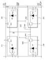
도 2를 참조하면, 4개의 픽셀들에 대응하는 등가 회로가 도시된다.Referring to Figure 2, an equivalent circuit corresponding to four pixels is shown.
RST 신호는 reset 동작을 지시하는 신호이고, ROW 신호는 어레이의 행(row)이 선택되었음을 알리는 신호이다. TR1, TR2, TR3, 및 TR4 신호들은 전달(transfer) 동작을 지시하는 신호들이다.The RST signal is a signal indicating a reset operation, and the ROW signal is a signal indicating that a row of the array has been selected. The TR1, TR2, TR3, and TR4 signals are signals that direct the transfer operation.
COL 노드(node)는 어레이의 열(column)에 대응하는 비트 라인 (bit line)이고, AN_BL 노드는 depth image를 획득하는 동작에서 TR1, TR2, TR3, 및 TR4 신호들과 상보적으로 제어될 수 있다.The COL node is a bit line corresponding to a column of the array and the AN_BL node can be complementarily controlled with the TR1, TR2, TR3, and TR4 signals in the operation of acquiring the depth image have.
픽셀(210)은 포토다이오드 D1, 제1 전달 트랜지스터 N11 및 제2 전달 트랜지스터 N12를 포함할 수 있다. 픽셀(220)은 포토다이오드 D2, 제1 전달 트랜지스터 N21 및 제2 전달 트랜지스터 N22를 포함할 수 있다. 픽셀(230)은 포토다이오드 D3, 제1 전달 트랜지스터 N31 및 제2 전달 트랜지스터 N32를 포함할 수 있다. 픽셀(240)은 포토다이오드 D4, 제1 전달 트랜지스터 N41 및 제2 전달 트랜지스터 N42를 포함할 수 있다.The
4개의 픽셀들(210, 220, 230, 240)은 리셋 트랜지스터 N51, 소스 팔로워(Source Follower) N61 및 선택 트랜지스터 N62를 공유할 수 있다.The four
픽셀(210)의 제1 전달 트랜지스터 N11는 TR1 신호에 기초하여 포토다이오드 D1에 의해 생성된 전하를 부유 확산 (Floating Diffusion, FD) 노드로 전달할 수 있다. 이 때 제1 전달 트랜지스터 N11는 TR1 신호에 기초하여 포토다이오드 D1 및 FD 노드를 전기적으로 연결하거나 차단할 수 있다. 제1 전달 트랜지스터 N11는 전 기 셔터와 같은 기능을 할 수 있다.The first transfer transistor N11 of the
픽셀(210)의 포토다이오드 D1는 빛을 감지할 수 있다. 포토다이오드 D1는 특정 필터와 결합하여 특정 파장 밴드의 빛을 감지할 수 있다. 포토다이오드 D1는 감지된 빛에 기초하여 전자 정공 쌍(Electron Hole Pair, EHP)을 생성할 수 있다.The photodiode D1 of the
제1 전달 트랜지스터 N11의 게이트 단자(gate terminal)는 TR1 신호에 연결되고 제1 전달 트랜지스터 N11의 드레인 단자(drain terminal)는 포토다이오드 D1에 연결되고 제1 전달 트랜지스터 N11의 소스 단자(source terminal)는 FD 노드에 연결된다.The gate terminal of the first transfer transistor N11 is connected to the TR1 signal, the drain terminal of the first transfer transistor N11 is connected to the photodiode D1 and the source terminal of the first transfer transistor N11 is connected to the drain terminal of the first transfer transistor N11 FD node.
포토다이오드 D1는 일반적인 포토다이오드 (n+ / psub 구조) 일 수도 있고 Pinned 포토다이오드 (p+ / n / psub 구조) 일 수도 있다. Pinned 포토다이오드는 동작 시 pinning voltage를 유지할 수 있고, Dark Current를 줄일 수 있다.The photodiode D1 may be a general photodiode (n + / psub structure) or a pinned photodiode (p + / n / psub structure). Pinned photodiodes can maintain pinning voltage during operation and reduce dark current.
픽셀(220)의 포토다이오드 D2는 감지된 빛에 기초하여 EHP를 생성할 수 있다. 픽셀(220)의 제1 전달 트랜지스터 N21는 TR2 신호에 기초하여 포토다이오드 D2에 의해 생성된 전하를 FD 노드로 전달할 수 있다. 이 때 제1 전달 트랜지스터 N21는 TR2 신호에 기초하여 포토다이오드 D2 및 FD 노드를 전기적으로 연결하거나 차단할 수 있다.The photodiode D2 of the
픽셀(220)의 제1 전달 트랜지스터 N21의 게이트 단자(gate terminal)는 TR2 신호에 연결되고 제1 전달 트랜지스터 N21의 드레인 단자(drain terminal)는 포토다이오드 D2에 연결되고 제1 전달 트랜지스터 N21의 소스 단자(source terminal)는 FD 노드에 연결된다.The gate terminal of the first transfer transistor N21 of the
픽셀(230)의 포토다이오드 D3는 감지된 빛에 기초하여 EHP를 생성할 수 있다. 픽셀(230)의 제1 전달 트랜지스터 N31는 TR3 신호에 기초하여 포토다이오드 D3에 의해 생성된 전하를 FD 노드로 전달할 수 있다. 이 때 제1 전달 트랜지스터 N31는 TR3 신호에 기초하여 포토다이오드 D3 및 FD 노드를 전기적으로 연결하거나 차단할 수 있다.The photodiode D3 of the
픽셀(230)의 제1 전달 트랜지스터 N31의 게이트 단자(gate terminal)는 TR3 신호에 연결되고 제1 전달 트랜지스터 N31의 드레인 단자(drain terminal)는 포토다이오드 D2에 연결되고 제1 전달 트랜지스터 N31의 소스 단자(source terminal)는 FD 노드에 연결된다.The gate terminal of the first transfer transistor N31 of the
픽셀(240)의 포토다이오드 D4는 감지된 빛에 기초하여 EHP를 생성할 수 있다. 픽셀(240)의 제1 전달 트랜지스터 N41는 TR4 신호에 기초하여 포토다이오드 D4에 의해 생성된 전하를 FD 노드로 전달할 수 있다. 이 때 제1 전달 트랜지스터 N41는 TR4 신호에 기초하여 포토다이오드 D4 및 FD 노드를 전기적으로 연결하거나 차단할 수 있다.The photodiode D4 of the
픽셀(240)의 제1 전달 트랜지스터 N41의 게이트 단자(gate terminal)는 TR4 신호에 연결되고 제1 전달 트랜지스터 N41의 드레인 단자(drain terminal)는 포토다이오드 D4에 연결되고 제1 전달 트랜지스터 N41의 소스 단자(source terminal)는 FD 노드에 연결된다.The gate terminal of the first transfer transistor N41 of the
소스 팔로워 N61의 게이트 단자는 FD 노드에 연결되고 소스 팔로워 N61의 드레인 단자는 전원(power) VDD에 연결되고 소스 팔로워 N61의 소스 단자는 선택 트 랜지스터 N62의 드레인 단자에 연결된다.The gate terminal of the source follower N61 is connected to the FD node, the drain terminal of the source follower N61 is connected to the power VDD, and the source terminal of the source follower N61 is connected to the drain terminal of the select transistor N62.
소스 팔로워 N61의 소스 단자의 전압은 FD 노드의 전압에 기초하여 결정될 수 있다. FD 노드의 전압은 픽셀들(210, 220, 230, 240) 중 적어도 하나 이상으로부터 전달된 전하의 양에 의하여 결정될 수 있다.The voltage of the source terminal of the source follower N61 can be determined based on the voltage of the FD node. The voltage at the FD node may be determined by the amount of charge transferred from at least one of the
선택 트랜지스터 N62의 게이트 단자는 행 제어 신호 ROW에 연결되고 선택 트랜지스터 N62의 드레인 단자는 소스 팔로워 N61의 소스 단자에 연결되고 선택 트랜지스터 N62의 소스 단자는 COL 노드( = bit line )에 연결된다.The gate terminal of the selection transistor N62 is connected to the row control signal ROW, the drain terminal of the selection transistor N62 is connected to the source terminal of the source follower N61, and the source terminal of the selection transistor N62 is connected to the COL node (= bit line).
행 제어 신호 ROW는 픽셀들(210, 220, 230, 240)에 의해 공유되는 FD 노드가 선택되었음을 알리는 기능을 할 수 있다. 행 제어 신호 ROW가 activate되면 소스 팔로워 N61 및 선택 트랜지스터 N62는 FD 노드의 전압에 기초하여 비트 라인을 구동(drive)할 수 있다.The row control signal ROW may serve to inform that the FD node shared by the
리셋 트랜지스터 N51의 게이트 단자는 RST 신호에 연결되고 리셋 트랜지스터 N51의 드레인 단자는 전원(power) VDD에 연결되고 리셋 트랜지스터 N51의 소스 단자는 FD 노드에 연결된다.The gate terminal of the reset transistor N51 is connected to the RST signal, the drain terminal of the reset transistor N51 is connected to the power VDD, and the source terminal of the reset transistor N51 is connected to the FD node.
FD 노드의 전압에 기초한 픽셀 정보 검출 과정이 수행된 후 RST 신호가 activate되면 리셋 트랜지스터 N51는 FD 노드의 전압을 전원 VDD로 reset할 수 있다.When the RST signal is activated after the pixel information detection process based on the voltage of the FD node is performed, the reset transistor N51 can reset the voltage of the FD node to the power supply VDD.
depth image를 획득하기 위한 과정은 다음과 같다. 이미지 센서가 depth image를 획득하는 depth frame에 대응하는 시간 구간은 제2 시간 구간으로 불릴 수 있음은 앞에서 설명한 바와 같다.The process for obtaining the depth image is as follows. The time interval corresponding to the depth frame at which the image sensor acquires the depth image can be referred to as a second time interval as described above.
픽셀들(210, 220, 230, 240)은 감지된 빛에 기초하여 생성된 전하를 FD 노드로 전달할 수 있다. 이 때 TR1, TR2, TR3 및 TR4 신호들은 동시에 activate될 수 있다.The
설명의 편의 상 TR1, TR2, TR3 및 TR4 신호들이 activate된 시간 구간을 활성(active) 시간 구간이라 명명한다. 반대로 TR1, TR2, TR3 및 TR4 신호들이 deactivate된 시간 구간을 비활성(inactive) 시간 구간이라 명명한다. 활성 시간 구간 및 비활성 시간 구간은 depth frame에 대응하는 시간 구간에 포함된다.For convenience of explanation, a time interval in which the TR1, TR2, TR3, and TR4 signals are activated is called an active time interval. Conversely, the time interval in which the TR1, TR2, TR3, and TR4 signals are deactivated is referred to as an inactive time interval. The active time interval and the inactivity time interval are included in the time interval corresponding to the depth frame.
이미지 센서는 물체와 이미지 센서 간의 거리 정보를 얻기 위하여 적외선을 조사(irradiate)할 수 있다. 이미지 센서는 주기적으로 적외선을 조사하고 조사하지 않는 동작을 한 번 이상 수행할 수 있다.The image sensor may irradiate infrared light to obtain distance information between the object and the image sensor. The image sensor can periodically perform an operation of irradiating and not irradiating infrared rays more than once.
이미지 센서는 적외선을 조사하는 시간 구간이 활성 시간 구간과 이루는 위상차를 0도, 90도, 180도 등으로 설정하여 depth image를 얻을 수 있다. 예를 들어, 도5에 도시된 바와 같이, 이미지 센서는 적외선을 조사하는 시간 구간을 활성 시간 구간과 일치시키고 적외선을 조사하지 않는 시간 구간을 비활성 시간 구간과 일치시킬 수 있다. 이 때 이미지 센서는 반사된 적외선을 감지하여 제1 정보를 획득할 수 있다. 제 1 정보 획득 후, 이미지 센서는 적외선을 조사하는 시간 구간을 비활성 시간 구간과 일치시키고 (이 때 적외선을 조사하는 시간 구간은 활성 시간 구간과는 180도의 위상 차이를 가짐) 적외선을 조사하지 않는 시간 구간을 활성 시간 구간과 일치시킬 수 있다. 이 때 이미지 센서는 반사된 적외선을 감지하여 제2 정보를 획득할 수 있다. 이미지 센서는 제1 정보 및 제2 정보에 기초하여 depth image를 획득할 수 있다. 이러한 방식을 indirect depth image 생성 방법이라고 할 수 있다.In the image sensor, the depth image can be obtained by setting the phase difference between the time interval for irradiating infrared rays with the active time interval to 0 degree, 90 degrees, 180 degrees, and so on. For example, as shown in FIG. 5, the image sensor may match a time interval for irradiating infrared rays with an active time interval and a time interval for not irradiating infrared rays with an inactivity time interval. At this time, the image sensor can detect the reflected infrared ray to acquire the first information. After acquiring the first information, the image sensor coincides the time period for irradiating the infrared ray with the inactivity time period (the time period for irradiating the infrared ray has a phase difference of 180 degrees from the active time period) The interval can be matched with the active time interval. At this time, the image sensor can sense the reflected infrared ray to acquire the second information. The image sensor may acquire a depth image based on the first information and the second information. This is the indirect depth image generation method.
포토다이오드들 D1, D2, D3 및 D4는 반사된 적외선을 감지하고, 감지된 적외선에 기초하여 EHP를 생성할 수 있다. 픽셀들(210, 220, 230, 240)의 제1 전달 트랜지스터들 N11, N21, N31, N41은 포토다이오드들 D1, D2, D3, D4에 의하여 상기 생성된 전하를 활성 시간 구간 동안 FD 노드로 전달할 수 있다. 픽셀들(210, 220, 230, 240)의 제2 전달 트랜지스터들 N12, N22, N32, N42은 포토다이오드들 D1, D2, D3, D4에 의하여 상기 생성된 전하를 비활성 시간 구간 동안 AN_BL 노드로 전달할 수 있다. 이미지 센서는 비활성 시간 구간 동안 AN_BL 노드의 전압을 전원 전압 VDD로 유지할 수 있다.The photodiodes D1, D2, D3 and D4 can sense the reflected infrared radiation and generate the EHP based on the sensed infrared radiation. The first transfer transistors N11, N21, N31 and N41 of the
반사된 적외선에 의해 생성된 EHP 중 일부는 활성 시간 구간 동안 FD 노드로 전달되고 나머지는 비활성 시간 구간 동안 AN_BL 노드로 전달될 수 있다. 적외선이 조사된 시점과 반사된 적외선이 감지된 시점의 차이를 time of flight (TOF) 라고 부르기도 하며, 반사된 적외선에 의해 생성된 EHP의 양 가운데 활성 시간 구간 동안 FD 노드로 전달되는 양의 비율은 TOF에 상응하는 양일 수 있다.Some of the EHPs generated by the reflected infrared may be delivered to the FD node during the active time interval and the rest may be delivered to the AN_BL node during the inactive time interval. The difference between the time when the infrared ray is irradiated and the time when the reflected infrared ray is detected is referred to as a time of flight (TOF), and the ratio of the amount of EHP generated by the reflected infrared ray to the amount of the FDH node May be an amount corresponding to TOF.
이미지 센서는 비활성 시간 구간 동안 감지된 적외선에 의해 생성된 EHP를 AN_BL 노드로 전달할 수 있다. 이 때 AN_BL 노드는 복수의 픽셀들에 대하여 공유될 수 있다. AN_BL 노드는 depth image 생성에 이용되지 않는 EHP의 sink path로서 기능할 수 있다.The image sensor can deliver the EHP generated by infrared detected during the inactivity time interval to the AN_BL node. At this time, the AN_BL node can be shared for a plurality of pixels. The AN_BL node can act as an EHP sink path that is not used to generate the depth image.
제2 전달 트랜지스터들 N12, N22, N32, N42 은 비활성 시간 구간 동안 depth image 생성에 이용되지 않는 EHP를 sink 또는 dump 하는 기능을 수행하므로 제1 전달 트랜지스터들 N11, N21, N31, N41 보다 작은 크기를 가질 수 있다.The second transfer transistors N12, N22, N32, and N42 perform a function of sinking or dumping EHP that is not used for the generation of the depth image during the inactive time interval, so that the second transfer transistors N12, N22, N32, Lt; / RTI >
이미지 센서는 depth image 를 획득하는 동안 4개의 픽셀들 (210, 220, 230, 240) 에 의하여 생성된 전하를 FD 노드에 저장함으로써 포토다이오드들 D1, D2, D3, D4의 낮은 적외선 감도에도 불구하고 depth image의 감도 및 SNR을 높일 수 있다.The image sensor stores the charges generated by the four
실시예에 따라서는 이미지 센서는 적외선을 활성 시간 구간보다 매우 짧은 시간 구간 동안 조사하고 반사된 적외선을 감지하여 depth image를 얻을 수 있다. 이 때 이미지 센서는 반사된 적외선을 감지하고, 감지된 적외선에 의하여 전하를 생성할 수 있다. 생성된 전하는 즉시 FD 노드 및 비트 라인을 경유하여 출력될 수 있다. 이미지 센서는 비트 라인에 전압의 변화가 생긴 시점 및 적외선이 조사된 시점 간의 차이에 관한 정보를 time to digital converter 등을 이용하여 직접적으로 얻을 수 있다. 이미지 센서는 얻어진 시점 차이 정보에 기초하여 TOF를 얻을 수 있다. 이처럼 부가적인 계산 과정 없이 depth image를 얻을 수 있는 방법을 direct depth image 생성 방법이라 할 수 있다.According to an embodiment, the image sensor may irradiate the infrared ray for a time period much shorter than the active time interval and detect the reflected infrared ray to obtain a depth image. At this time, the image sensor can sense the reflected infrared ray and generate the electric charge by the sensed infrared ray. The generated charge can be immediately output via the FD node and the bit line. The image sensor can directly obtain information on a difference between a point of time when the voltage of the bit line changes and a point of time when the infrared ray is irradiated using a time to digital converter. The image sensor can obtain the TOF based on the obtained time difference information. A method of generating a depth image without additional computation is called a direct depth image generation method.
이미지 센서는 적외선을 조사하는 동작 없이 픽셀들(210, 220, 230, 240)을 이용하여 color image를 얻을 수 있다.The image sensor can obtain the color image using the
이미지 센서는 픽셀(210)을 이용하여 적색 영상을 얻을 수 있다. 적색 영상을 획득하는 시간 구간 동안 TR1 신호는 activate 되고, TR2, TR3, TR4 신호는 deactivate 될 수 있다. 이 때 포토다이오드 D1는 적색 및 적외선을 감지할 수 있 는 필터와 결합될 수 있다.The image sensor can obtain a red image using the
이미지 센서는 픽셀(220)을 이용하여 녹색 영상(1)을 얻을 수 있다. 녹색 영상(1)을 획득하는 시간 구간 동안 TR2 신호는 activate 되고, TR1, TR3, TR4 신호는 deactivate 될 수 있다. 이 때 포토다이오드 D2는 녹색 및 적외선을 감지할 수 있는 필터와 결합될 수 있다.The image sensor can obtain the green image (1) using the pixel (220). The TR2 signal can be activated and the TR1, TR3, and TR4 signals can be deactivated during the time period of acquiring the green image (1). At this time, the photodiode D2 can be combined with a filter capable of sensing green and infrared rays.
이미지 센서는 픽셀(230)을 이용하여 녹색 영상(2)을 얻을 수 있다. 녹색 영상(2)을 획득하는 시간 구간 동안 TR3 신호는 activate 되고, TR1, TR2, TR4 신호는 deactivate 될 수 있다. 이 때 포토다이오드 D3는 녹색 및 적외선을 감지할 수 있는 필터와 결합될 수 있다.The image sensor can obtain the green image (2) using the pixel (230). The TR3 signal can be activated and the TR1, TR2, and TR4 signals can be deactivated during the time period of acquiring the green image (2). At this time, the photodiode D3 may be combined with a filter capable of sensing green and infrared rays.
이미지 센서는 픽셀(240)을 이용하여 청색 영상을 얻을 수 있다. 청색 영상을 획득하는 시간 구간 동안 TR4 신호는 activate 되고, TR1, TR2, TR3 신호는 deactivate 될 수 있다. 이 때 포토다이오드 D4는 청색 및 적외선을 감지할 수 있는 필터와 결합될 수 있다.The image sensor can obtain a blue image using the
이미지 센서는 color image를 얻는 동안 제2 트랜지스터들 N12, N22, N32, N42을 이용하여 blooming 현상을 방지할 수 있다. blooming 현상은 빛이 매우 강한 경우 생길 수 있다.The image sensor can prevent the blooming phenomenon by using the second transistors N12, N22, N32 and N42 while obtaining the color image. The blooming phenomenon can occur when the light is very strong.
이미지 센서의 픽셀들 각각은 제1 전달 트랜지스터 및 제2 전달 트랜지스터를 포함하고, 이미지 센서의 4개의 픽셀들은 리셋 트랜지스터 및 2개의 선택 구동 트랜지스터들을 공유할 수 있다. 따라서 픽셀들 각각은 2.75 개의 트랜지스터를 포함하는 것으로 간주될 수 있다.Each of the pixels of the image sensor includes a first transfer transistor and a second transfer transistor, and the four pixels of the image sensor may share a reset transistor and two select driving transistors. Thus, each of the pixels may be considered to comprise 2.75 transistors.
실시예에 따라서는 이미지 센서는 depth image를 생성하기 위하여 특정 밴드의 빛을 조사하고, 상기 조사된 빛이 물체에 의하여 반사되면 상기 반사된 빛을 감지할 수 있다. depth image를 생성하기 위하여 조사되는 빛은 적외선에 국한되지 않고 픽셀들과 결합되는 필터의 특성에 기초하여 결정될 수 있다.According to an embodiment, the image sensor may irradiate light of a specific band to generate a depth image, and may sense the reflected light when the irradiated light is reflected by the object. The light irradiated to create the depth image may be determined based on the characteristics of the filter coupled with the pixels, not limited to infrared radiation.
도 2에서는 4개의 픽셀들이 하나의 FD 노드 및 트랜지스터들을 공유하는 구조가 도시되었으나 실시예에 따라서는 하나의 FD 노드를 공유하는 픽셀들의 개수는 depth image의 공간 해상도에 따라 결정될 수 있다.Although FIG. 2 shows a structure in which four pixels share one FD node and transistors, according to an embodiment, the number of pixels sharing one FD node may be determined according to the spatial resolution of the depth image.
포토다이오드 D1에 의해 생성된 전하가 FD 노드로 전달되기 위해서는 트랜지스터 N11의 드레인 단자 (포토다이오드 D1에 연결된) 및 FD 노드 간의 전위차가 유지되어야 한다. 포토다이오드 D1에 의해 생성된 전하가 FD 노드로 전달되는 과정에서 N11의 드레인 단자의 전압 및 FD 노드의 전압이 변화되면 포토다이오드 D1에 의해 생성된 모든 전하가 FD 노드로 전달되지 못할 수 있다. 이 같은 이유로 포토다이오드 D1의 감도가 낮아질 수 있다.In order for the charge generated by the photodiode D1 to be transferred to the FD node, the potential difference between the drain terminal (connected to the photodiode D1) of the transistor N11 and the FD node must be maintained. If the voltage of the drain terminal of N11 and the voltage of the FD node are changed in the process of transferring the charge generated by the photodiode D1 to the FD node, all charges generated by the photodiode D1 may not be transferred to the FD node. For this reason, the sensitivity of the photodiode D1 can be lowered.
포토다이오드 D1이 PINNED 포토다이오드인 경우 포토다이오드 D1의 전압은 광량에 따라 PINNING 전압 이하에서 결정되므로 FD 노드의 전압에 비해 낮을 수 있다. 따라서 포토다이오드 D1이 PINNED 포토다이오드인 경우 포토다이오드 D1에 의해 생성된 전하는 TR1이 activate 된 동안 모두 FD 노드로 전달될 수 있다. 이 경우 포토다이오드 D1의 감도를 높일 수 있다.If the photodiode D1 is a PINNED photodiode, the voltage of the photodiode D1 may be lower than the voltage of the FD node since it is determined below the PINNING voltage according to the amount of light. Thus, if the photodiode D1 is a PINNED photodiode, the charge generated by the photodiode D1 may be transferred to the FD node while TR1 is activated. In this case, the sensitivity of the photodiode D1 can be increased.
도 3은 도 2의 등가 회로에 대응하는 반도체 소자의 일 예의 일부의 단면을 도시한다.Fig. 3 shows a cross-section of a part of an example of a semiconductor element corresponding to the equivalent circuit of Fig.
도 3을 참조하면 도 2의 포토다이오드 D1는 P+ / N- / P-substrate 의 구조를 가지는 PINNED 포토다이오드이다.Referring to FIG. 3, the photodiode D1 of FIG. 2 is a PINNED photodiode having a structure of P + / N- / P-substrate.
도 3을 참조하면 도 2의 트랜지스터 N11의 게이트 단자는 TR 신호에 연결될 수 있다. 트랜지스터 N11의 소스 단자는 FD 노드에 연결될 수 있다.Referring to FIG. 3, the gate terminal of the transistor N11 of FIG. 2 may be coupled to the TR signal. The source terminal of transistor N11 may be connected to the FD node.
도 3을 참조하면 도 2의 리셋 트랜지스터 N51의 게이트 단자는 RST 신호에 연결될 수 있고 N51의 드레인 단자는 전원 VDD에 연결될 수 있고 N51의 소스 단자는 FD 노드에 연결될 수 있다.Referring to FIG. 3, the gate terminal of the reset transistor N51 of FIG. 2 may be coupled to the RST signal, the drain terminal of N51 may be coupled to the power supply VDD, and the source terminal of N51 may be coupled to the FD node.
도 4는 본 발명의 다른 실시예에 따른 광원 및 이미지 센서를 포함하는 이미징 장치(imaging device)의 제어 방법을 도시하는 도면이다.4 is a diagram showing a control method of an imaging device including a light source and an image sensor according to another embodiment of the present invention.
도 4를 참조하면, 제어 방법은 화소(pixel) 정보를 리셋한다(S410).Referring to FIG. 4, the control method resets pixel information (S410).
리셋 단계(S410) 이후, 색상 프레임에 대응하는 시간 구간 동안 적외선을 조사하지 않는다(S420).After the resetting step S410, the infrared ray is not irradiated during the time interval corresponding to the color frame (S420).
적외선을 조사하지 않고 감지된 빛에 기초하여 가시 광선 정보(A)를 취득한다(S430). 가시 광선 정보(A)를 취득하는 단계(S430)는 전술한 바와 같이, 적외선에 의한 잡음을 제거하는 적절한 후처리 과정을 포함할 수 있다.The visible light information A is acquired based on the sensed light without irradiating the infrared ray (S430). The step S430 of obtaining the visible light information A may include an appropriate post-processing to remove noise due to infrared rays, as described above.
단계(S410) 내지 단계(S430)는 전술한 제1 시간 구간 동안 수행될 수 있으며, 단계(S430)에서 취득한 가시 광선 정보(A)에 기초하여 color 영상을 생성한다(S470).Steps S410 to S430 may be performed during the first time period described above, and a color image is generated based on the visible light information A acquired in step S430 (S470).
가시 광선 정보(A) 취득 후, 이미징 장치의 광원은 특정 주파수로 변조된 적외선을 조사하고(S440), 물체에 의해 반사된 적외선 정보(B1)를 취득한다(S451). 이 때, 단계(S451)는 단계(S440)와 0도의 위상 차이를 가지는 펄스에 의하여 수행될 수 있다.After obtaining the visible light information A, the light source of the imaging apparatus irradiates the infrared ray modulated at a specific frequency (S440), and obtains the infrared ray information B1 reflected by the object (S451). At this time, step S451 may be performed by a pulse having a phase difference of 0 degrees with step S440.
단계(S451)가 수행된 후 이미징 장치의 광원은 특정 주파수로 변조된 적외선을 조사하고(S452),After the step S451 is performed, the light source of the imaging apparatus irradiates the infrared ray modulated at a specific frequency (S452)
반사된 적외선 정보(B2)를 취득한다(S453). 이 때 단계(S453)는 단계(S452)와 180도의 위상 차이를 가지는 펄스에 의하여 수행될 수 있다.And obtains the reflected infrared information B2 (S453). At this time, step S453 may be performed by a pulse having a phase difference of 180 degrees with step S452.
반사된 적외선 정보(B1, B2)에 기초하여 Depth 정보를 생성한다(S454). Depth 정보를 생성하는 단계(S454)는 전술한 바와 같이, 가시광선 및 광원으로부터 조사되지 않은 적외선에 의한 잡음을 제거하는 과정을 포함할 수 있다.Depth information is generated based on the reflected infrared information B1 and B2 (S454). As described above, the step of generating the depth information S454 may include a process of removing visible light and noise due to infrared rays not irradiated from the light source.
단계(S440) 내지 단계(S454)는 제2 시간 구간 동안 수행될 수 있으며, 단계(S454)에서 생성된 Depth 정보에 기초하여 Depth 영상을 생성한다(S460).Steps S440 to S454 may be performed during the second time period, and a Depth image is generated based on the Depth information generated in step S454 (S460).
단계(S460) 및 단계(S470)는 제2 시간 구간 동안 수행될 수도 있고, 다음 영상 프레임의 제1 시간 구간 동안 수행될 수도 있다.Steps S460 and S470 may be performed during the second time interval or during the first time interval of the next image frame.
가시 광선 정보(A)를 취득하는 단계(S410) 내지 단계(S430) 및/또는 반사된 적외선 정보(B1, B2)를 생성하는 단계(S440)내지 단계(S454)는 반복 수행될 수 있고, 반복 수행된 값의 평균을 계산하여 가시광선 정보(A) 및/또는 반사된 적외선 정보(B1,B2)로 사용할 수 있다.Steps S440 to S445 of obtaining the visible light information A and / or generating the reflected infrared information B1 and B2 may be repeatedly performed, The average of the performed values can be calculated and used as the visible light information A and / or the reflected infrared information B1 and B2.
도 5는 도 2의 이미지 센서의 동작의 일 예를 도시하는 타이밍도이다.5 is a timing chart showing an example of the operation of the image sensor of Fig.
도 5를 참조하면 이미지 센서는 color image를 얻기 전에 RST, TR1, TR2, TR3 및 TR4를 activate하여 픽셀들(210, 220, 230, 240) 각각을 리셋한다.Referring to FIG. 5, the image sensor activates RST, TR1, TR2, TR3, and TR4 before obtaining a color image to reset each of the
이미지 센서는 integration time Tint_color 동안 빛에 의해 생긴 전하를 포토다이오드들(D1, D2, D3, D4) 각각의 기생 커패시턴스(parasitic capacitance)에 저장할 수 있다.The image sensor may store the integration time Tint_color picture of the charge caused by the light diode for (D1, D2, D3, D4 ) , each of the parasitic capacitance (parasitic capacitance).
Tint_color 가 종료된 후 칼라 획득 시간 Tread_color 가 시작될 수 있다. Tint_color 및 Tread_color 는 제1 시간 구간 (color frame에 대응하는 시간 구간)을 형성할 수 있다.Tint_ after the endcolor may begin collar acquisition time Tread_color. T_intcolorread_color and T may form a first time interval (time interval corresponding to the color frame).
이미지 센서는 Tint_color 후 ROW 신호 및 RST 신호를 activate하여 FD 노드를 리셋할 수 있다. 이미지 센서는 이 때의 FD 노드의 전압 Vrst_color(1) 을 검출할 수 있다. Vrst_color(1)는 리셋된 FD 노드의 오프셋 전압으로서 잡음에 의한 영향을 제거한 칼라 정보를 얻기 위하여 이용될 수 있다.The image sensor may reset the FD node to activate the ROW signal and the RST signal after T_intcolor. The image sensor may detect voltage V_rstcolor (1) of the FD node at that time. Vrst_color (1) can be used as offset voltage of the reset FD node to obtain the color information from which noise influence is removed.
이미지 센서는 Vrst_color(1) 을 검출한 후 TR1 신호를 activate하여 포토다이오드 D1의 기생 커패시턴스에 저장된 전하를 FD 노드로 전달할 수 있다. 이미지 센서는 이 때의 FD 노드의 전압 Vsig_color(1) 을 검출할 수 있다. D1이 적색 필터와 결합된 경우 전압 Vsig_color(1)는 적색 영상에 대응하는 raw data일 수 있다.The image sensor may then detect the Vrst_color (1) to activate the TR1 signal to pass an electric charge stored in the parasitic capacitance of the photodiode D1 to the FD node. The image sensor may detect voltage Vsig_color (1) of the FD node at that time. When D1 is combined with the red filter, the voltage Vsig_color (1) may be the raw data corresponding to the red image.
이미지 센서는 Vsig_color(1) 을 검출한 후 RST 신호를 activate하여 FD 노드를 리셋할 수 있다. 이미지 센서는 이 때의 FD 노드의 전압 Vrst_color(2) 을 검출할 수 있다. Vrst_color(2)는 또 다른 오프셋 전압일 수 있다.The image sensor may reset the FD node, after detecting the Vsig_color (1) to activate the RST signal. The image sensor may detect voltage V_rstcolor (2) of the FD node at that time. Vrst_color (2) may be another offset voltage.
이미지 센서는 Vrst_color(2) 을 검출한 후 TR2 신호를 activate하여 포토다이오드 D2의 기생 커패시턴스에 저장된 전하를 FD 노드로 전달할 수 있다. 이미지 센서는 이 때의 FD 노드의 전압 Vsig_color(2) 을 검출할 수 있다. D2가 녹색 필터와 결합된 경우 전압 Vsig_color(2)는 녹색 영상에 대응하는 raw data일 수 있다.The image sensor may then detect the Vrst_color (2) to activate the TR2 signal to pass an electric charge stored in the parasitic capacitance of the photodiode D2 to the FD node. The image sensor may detect voltage Vsig_color (2) of the FD node at that time. When D2 is combined with the green filter, the voltage Vsig_color (2) may be the raw data corresponding to the green image.
이미지 센서는 Vsig_color(2) 을 검출한 후 RST 신호를 activate하여 FD 노드를 리셋할 수 있다. 이미지 센서는 이 때의 FD 노드의 전압 Vrst_color(3) 을 검출할 수 있다. Vrst_color(3)는 또 다른 오프셋 전압일 수 있다.The image sensor may reset the FD node, after detecting the Vsig_color (2) to activate the RST signal. The image sensor may detect voltage V_rstcolor (3) of the FD node at that time. Vrst_color (3) may be another offset voltage.
이미지 센서는 Vrst_color(3) 을 검출한 후 TR3 신호를 activate하여 포토다이오드 D3의 기생 커패시턴스에 저장된 전하를 FD 노드로 전달할 수 있다. 이미지 센서는 이 때의 FD 노드의 전압 Vsig_color(3) 을 검출할 수 있다. D3가 녹색 필터와 결합된 경우 전압 Vsig_color(3)는 녹색 영상에 대응하는 또 다른 raw data일 수 있다.The image sensor may then detect the Vrst_color (3) to activate the TR3 signal to pass an electric charge stored in the parasitic capacitance of the photodiode D3 to the FD node. The image sensor may detect voltage Vsig_color (3) of the FD node at that time. When D3 is combined with the green filter, the voltage Vsig_color (3) may be another raw data corresponding to the green image.
이미지 센서는 Vsig_color(3) 을 검출한 후 RST 신호를 activate하여 FD 노드를 리셋할 수 있다. 이미지 센서는 이 때의 FD 노드의 전압 Vrst_color(4) 을 검출할 수 있다. Vrst_color(4)는 또 다른 오프셋 전압일 수 있다.The image sensor may reset the FD node, after detecting the Vsig_color (3) to activate the RST signal. The image sensor may detect voltage V_rstcolor (4) of the FD node at that time. Vrst_color (4) may be another offset voltage.
이미지 센서는 Vrst_color(4) 을 검출한 후 TR4 신호를 activate하여 포토다이 오드 D4의 기생 커패시턴스에 저장된 전하를 FD 노드로 전달할 수 있다. 이미지 센서는 이 때의 FD 노드의 전압 Vsig_color(4) 을 검출할 수 있다. D4가 청색 필터와 결합된 경우 전압 Vsig_color(4)는 청색 영상에 대응하는 raw data일 수 있다.The image sensor may then detect the Vrst_color (4) to activate the TR4 signal to pass an electric charge stored in the parasitic capacitance of the photo diode D4 to the FD node. The image sensor may detect voltage Vsig_color (4) of the FD node at that time. When D4 is combined with the blue filter, the voltage Vsig_color (4) may be the raw data corresponding to the blue image.
이미지 센서는 상기 검출된 Vrst_color(1) 및 Vsig_color(1)에 correlated doubling sampling을 수행하고, 상기 검출된 Vrst_color(1) 및 Vsig_color(1)의 차이를 계산할 수 있다. 이미지 센서는 상기 계산된 차이로부터 적색 영상을 얻을 수 있다.The image sensor is the difference between Vrst_color (1) and Vsig_ the performing correlated doubling sampling thecolor (1) and the detection Vrst_color (1) and Vsig_color (1) the detected Can be calculated. The image sensor may obtain a red image from the calculated difference.
마찬가지로 이미지 센서는 상기 검출된 Vrst_color(2) 및 Vsig_color(2)에 correlated doubling sampling을 수행하고, 상기 검출된 Vrst_color(2) 및 Vsig_color(2)의 차이를 계산할 수 있다. 또한 이미지 센서는 상기 검출된 Vrst_color(3) 및 Vsig_color(3)에 correlated doubling sampling을 수행하고, 상기 검출된 Vrst_color(3) 및 Vsig_color(3)의 차이를 계산할 수 있다. 이미지 센서는 상기 계산된 차이에 기초하여 녹색 영상을 얻을 수 있다.Similarly, the image sensor is the detected Vrst_color (2), and Vsig_ perform correlated doubling sampling incolor (2), and the difference between the detected Vrst_color (2), and Vsig_color (2) Can be calculated. In addition, the image sensor is the detected Vrst_color (3), and Vsig_ perform correlated doubling sampling thecolor (3), and a difference between the detected Vrst_color (3), and Vsig_color (3) Can be calculated. The image sensor can obtain a green image based on the calculated difference.
이미지 센서는 상기 검출된 Vrst_color(4) 및 Vsig_color(4)에 correlated doubling sampling을 수행하고, 상기 검출된 Vrst_color(4) 및 Vsig_color(4)의 차이를 계산할 수 있다. 이미지 센서는 상기 계산된 차이로부터 청색 영상을 얻을 수 있다.The image sensor is the difference between Vrst_color (4), and Vsig_ the performing correlated doubling sampling thecolor (4), said detection Vrst_color (4), and Vsig_color (4) the detected Can be calculated. The image sensor can obtain a blue image from the calculated difference.
이미지 센서는 correlated doubling sampling을 수행함으로써 픽셀들 각각의 트랜지스터들의 편차에서 기인하는 fixed pattern noise 또는 1/f noise 등을 제거 할 수 있다. 이미지 센서는 Tread_color 시간 구간 동안 PINNED 포토다이오드의 PINNING 전압에 기초하여 blooming 현상이 일어나지 않도록 AN_BL 노드의 전압을 최적화된 전압으로 유지할 수 있다.The image sensor performs correlated doubling sampling to remove fixed pattern noise or 1 / f noise due to the deviation of each of the pixels. The image sensor may maintain a voltage of optimizing the voltage of the node AN_BL prevent the blooming phenomenon based on a voltage of PINNING PINNED photodiode during the time interval Tread_color occur.
Color 영상을 얻은 후 depth 영상을 얻기 위해서는 변조된 주파수의 적외선 펄스를 조사하고 반사되어 돌아온 적외선을 검출하는 과정이 필요하다. Depth frame에 대응하는 과정은 제1 측정 과정과 제2 측정 과정을 포함할 수 있다. 제1 측정 과정은 다음과 같이 수행될 수 있다. 먼저 이미지 센서는 시간 구간 Tint_depth1 동안 변조된 적외선 펄스와 동일한 위상을 가지도록 TR 신호(TR1, TR2, TR3, TR4)를 activate하여 반사된 적외선에 의해 발생한 전하를 FD 노드에 저장할 수 있다. 이 때 4개의 픽셀들(210, 220, 230, 240)은 하나의 픽셀과 같이 기능할 수 있다. 제1 측정 과정에 대응하는 시간 구간은 도 5에서 시간 구간 Tint_depth1 및 시간 구간 Tread_depth1으로 표시된다. 시간 구간 Tread_depth1 동안 이미지 센서는 FD 노드를 리셋함과 동시에 시간 구간 Tint_depth1 동안 측정된 깊이 값을 처리하여 제1 측정 과정에 대응하는 깊이 정보를 생성할 수 있다. 일반적인 포토다이오드는 적외선에 대한 감도가 가시광선에 대한 감도보다 매우 낮으므로 이를 해결하기 위해 이미지 센서는 4개의 포토다이오드들(D1, D2, D3, D4)에서 생성된 전하를 상기 하나의 FD 노드로 전달함으로써 4배 향상된 감도를 구현할 수 있다.To obtain the depth image after obtaining the color image, it is necessary to investigate the infrared ray of the modulated frequency and to detect the reflected infrared ray. The process corresponding to the depth frame may include a first measurement process and a second measurement process. The first measurement process can be performed as follows. First, the image sensor may also store the charges generated by the infrared rays reflected activate the time interval Tint_depth1 the TR signals to have the same phase as the infrared pulses (TR1, TR2, TR3, TR4 ) modulation for the FD node. At this time, the four
이미지 센서는 적외선이 조사되지 않는 시간에는 TR 신호(TR1, TR2, TR3, TR4)를 deactivate하고 AN_BL 노드의 전압을 상대적으로 높게 유지할 수 있다. 적외선이 조사되지 않는 동안 생성된 전하는 제2 전달 트랜지스터 N12, N22, N32, N42를 경유하여 AN_BL 노드로 방전되고 FD 노드로 전달되지 않는다. 이미지 센서는 적외선이 조사되는 동안 AN_BL 노드의 전압을 상대적으로 낮게 유지하여 적외선에 의해 생성된 전하가 AN_BL 노드로 방전되지 않도록 할 수 있다. 적외선이 조사되는 동안 반사된 적외선에 의해 생성된 전하는 모두 FD 노드에 전달될 수 있다. 적외선 펄스의 주파수는 수 MHz ~ 수십 MHz로 매우 빠르기 때문에 조사되는 시간이 매우 짧아 그 시간 안에 blooming이 일어날 확률은 매우 낮으므로 이미지 센서는 적외선을 조사하는 동안 AN_BL 노드의 전압을 충분히 낮게 설정할 수 있다. 또한 발생한 전하의 양이 매우 적으므로 이미지 센서는 전하를 FD 노드에 전달하는 과정을 Tint_depth1 동안 N번 수행할 수 있다. 이미지 센서는 N번 수행된 전달 과정을 통해 FD 노드에 전하를 축적할 수 있다. 이미지 센서는 Tint_depth1 후 FD 노드의 전압을 검출하고 FD 노드 및 포토다이오드들(D1, D2, D3, D4) 각각을 리셋할 수 있다.The image sensor deactivates the TR signals (TR1, TR2, TR3, TR4) and maintains the voltage of the AN_BL node relatively high when the infrared ray is not irradiated. The charge generated while the infrared ray is not irradiated is discharged to the AN_BL node via the second transfer transistors N12, N22, N32, N42 and is not transferred to the FD node. The image sensor can maintain the voltage of the AN_BL node relatively low while the infrared rays are irradiated so that the charge generated by the infrared rays can not be discharged to the AN_BL node. All the electric charges generated by the reflected infrared rays while the infrared ray is irradiated can be transmitted to the FD node. Since the frequency of infrared pulses is very fast from several MHz to several tens of MHz, the time of irradiation is very short and the probability of blooming in that time is very low, so the image sensor can set the voltage of the AN_BL node sufficiently low while irradiating infrared rays. Also, since the amount of charge generated is very small, the image sensor can perform the process of transferring the charge to the FD node N times during Tint_depth 1 . The image sensor can accumulate charge on the FD node through the transfer process performed N times. The image sensor can detect the voltage of the FD node and reset the FD node and the photodiodes (D1, D2, D3, D4) after Tint_depth1 .
제2 측정 과정은 다음과 같이 수행될 수 있다. 이미지 센서는 시간 구간 Tint_depth2 동안 변조된 적외선 펄스와 180도의 위상 차이를 가지도록 TR 신호(TR1, TR2, TR3, TR4)를 activate하여 반사된 적외선에 의해 발생한 전하를 FD 노드에 저장할 수 있다. 이미지 센서는 이 같은 동작을 Tint_depth2 동안 N번 수행할 수 있다.The second measurement process can be performed as follows. The image sensor may store charges generated by the infrared rays reflected activate the time interval Tint_depth2 TR signals (TR1, TR2, TR3, TR4 ) to have the infrared pulse and the 180-degree phase difference between modulation for the FD node . The image sensor can perform this operation N times during Tint_depth 2 .
제2 측정 과정에 대응하는 시간 구간은 도 5에서 시간 구간 Tint_depth2 및 시 간 구간 Tread_depth2으로 표시된다. 시간 구간 Tread_depth2 동안 이미지 센서는 FD 노드를 리셋함과 동시에 시간 구간 Tint_depth2 동안 측정된 깊이 값을 처리하여 제2 측정 과정에 대응하는 깊이 정보를 생성할 수 있다.The time interval corresponding to the second measurement process is represented by a time interval Tint_depth 2 and a time interval Tread_depth 2 in FIG. During time interval Tread_depth2 image sensor may generate depth information corresponding to the second measurement process to also reset the FD node and at the same time, process a depth value measured during the time interval Tint_depth2.
이미지 센서는 제1 측정 과정에서 변조된 적외선 펄스와 0도의 위상 차이를 가지도록 TR 신호를 제어하여 FD 노드의 전압을 검출하고, 제2 측정 과정에서 변조된 적외선 펄스와 180도 (실시예에 따라서는 90도도 가능하다) 의 위상 차이를 가지도록 TR 신호를 제어하여 FD 노드의 전압을 검출할 수 있다. 이미지 센서는 제1 측정 과정 및 제2 측정 과정을 수행함으로써 두 번 FD 노드의 전압을 검출하고, 각각의 깊이 정보를 생성할 수 있다. 이미지 센서는 제1 측정 과정에 대응하는 깊이 정보 및 제2 측정 과정에 대응하는 깊이 정보에 기초하여 물체의 반사도가 거리 측정에 미치는 영향을 제거하고 depth image를 생성할 수 있다.The image sensor detects the voltage of the FD node by controlling the TR signal so as to have a phase difference of 0 degrees with the infrared pulse modulated in the first measurement step and detects the voltage of the FD node by 180 degrees with respect to the modulated infrared pulse The voltage of the FD node can be detected by controlling the TR signal to have a phase difference of 90 degrees. The image sensor can detect the voltage of the FD node twice and generate the depth information of each FD by performing the first measurement process and the second measurement process. The image sensor can remove the influence of the reflectivity of the object on the distance measurement based on the depth information corresponding to the first measurement process and the depth information corresponding to the second measurement process and generate the depth image.
도 6은 도 5의 동작의 일부를 상세히 도시하는 도면이다.Fig. 6 is a diagram showing a part of the operation of Fig. 5 in detail.
도 6을 참조하면 waveform(610)은 반사된 적외선을 도시한다.Referring to FIG. 6, a
waveform(620)은 Tint_depth1 동안 인가되는 TR 신호를 도시한다.Waveform 620 shows the TR signal applied during
waveform(630)은 Tint_depth2 동안 인가되는 TR 신호를 도시한다.Waveform 630 shows the TR signal applied during Tint_depth 2 .
Tdep는 적외선이 조사되는 시간 구간을 나타낸다. 빗금 부분은 반사된 적외선에 의하여 생성된 전하 중 FD 노드에 전달되는 양을 나타낸다.Tdep represents the time interval during which infrared rays are irradiated. The hatched portion represents the amount of charge generated by the reflected infrared rays and transmitted to the FD node.
TTOF는 조사된 적외선이 물체에 의하여 반사되고, 반사된 적외선이 이미지 센 서에 의하여 감지될 때까지의 시간을 나타낸다.TTOF represents the time until the irradiated infrared ray is reflected by the object and the reflected infrared ray is detected by the image sensor.
Tint_depth1 동안 수행되는 동작을 제1 측정 과정, Tint_depth2 동안 수행되는 동작을 제2 측정 과정이라 하면, 이미지 센서는 제1 측정 과정에서는 Tdep - TTOF 동안 전하를 FD 노드로 전달할 수 있고, 제2 측정 과정에서는 TTOF 동안 전하를 FD 노드로 전달할 수 있다.Tint_depth1 operating a first measurement process is performed for, Tint_ when as operating a second measurement process are performed whiledepth2, the image sensor is a first measurement process, Tdep - pass the charge during TTOF is FD node And during the second measurement process, the charge can be transferred to the FD node during the TTOF .
포토다이오드 D1는 적외선뿐만 아니라 적색 광선도 감지할 수 있고, 포토다이오드 D2 및 D3는 적외선뿐만 아니라 녹색 광선도 감지할 수 있고, 포토다이오드 D4는 적외선뿐만 아니라 청색 광선도 감지할 수 있다. 따라서, 제1 측정 과정의 각 펄스에 의하여 FD 노드에 저장되는 전하 Qdep1는 하기 수학식 1과 같이 나타내어진다.The photodiode D1 can detect infrared rays as well as red light rays. The photodiodes D2 and D3 can sense not only infrared rays but also green rays, and the photodiode D4 can detect not only infrared rays but also blue rays. Therefore, the charge Qdep1 stored in the FD node by each pulse in the first measurement process is expressed by the following equation (1).
[수학식 1][Equation 1]
Qdep1 = Tdep x ( ir + ig1 + ig2 + ib ) + ( Tdep - TTOF ) x iirQdep1 = Tdep x (ir + ig1 + ig2 + ib ) + (Tdep - TTOF ) x iir
여기서 ir 는 포토다이오드 D1에 의하여 생성되는 photocurrent를 나타내고, ig1 는 포토다이오드 D2에 의하여 생성되는 photocurrent를 나타내고, ig2는 포토다이오드 D3에 의하여 생성되는 photocurrent를 나타내고, ib는 포토다이오드 D4에 의하여 생성되는 photocurrent를 나타낸다. iir는 포토다이오드 D1, D2, D3, D4에 의하여 생성되는 photocurrent를 나타낸다.Where ir denotes the photocurrent generated by the photodiode D1, ig1 denotes the photocurrent generated by the photodiode D2, ig2 denotes the photocurrent generated by the photodiode D3, and ib denotes the photocurrent generated by the photodiode D4 It represents the photocurrent generated by the photocurrent. iir represents photocurrent generated by photodiodes D1, D2, D3, and D4.
제2 측정 과정의 각 펄스에 의하여 FD 노드에 저장되는 전하 Qdep2는 하기 수학식 2와 같이 나타내어진다.The charge Qdep2 stored in the FD node by each pulse of the second measurement process is expressed by the following equation (2).
[수학식 2]&Quot; (2) "
Qdep2 = Tdep x ( ir + ig1 + ig2 + ib ) + TTOF x iirQdep2 = Tdep x (ir + ig1 + ig2 + ib ) + TTOF x iir
이미지 센서는 Tread_color 시간 구간 동안 획득한 color image 정보를 이용하여 가시 광선에 의한 영향을 제거할 수 있다. color 획득 시 저장된 전하 Qcol는 하기 수학식 3과 같이 나타내어진다.The image sensor may use a color image information obtained during the time interval Tread_color remove the influence of the visible light. the chargeQcol stored at the time of color acquisition is expressed by
[수학식 3]&Quot; (3) "
Qcol = Tcol x ( ir + ig1 + ig2 + ib )Col =col T x Q (i +r ig1 +g2 i +b i)
여기서 Tcol는 color integration time이고, Tdep 및 Tcol 간에는 일정한 비례 관계가 성립하므로 이 관계를 하기 수학식 4와 같이 나타낼 수 있다.Here, Tcol is a color integration time, and a constant proportional relationship is established between Tdep and Tcol, so that this relationship can be expressed by Equation (4).
[수학식 4]&Quot; (4) "
Tdep = k x TcolTdep = k x Tcol
여기서 k는 비례 상수이다.Where k is a proportional constant.
상기 수학식 1, 수학식 2, 수학식 3 및 수학식 4를 조합함으로써 하기 수학식 5를 얻을 수 있다.By combining the above Equations (1), (2), (3) and (4), the following Equation (5) can be obtained.
[수학식 5]&Quot; (5) "

상기 수학식 5를 변형하면 하기 수학식 6을 얻을 수 있다.By modifying Equation (5), Equation (6) can be obtained.
[수학식 6]&Quot; (6) "

이미지 센서는 상기 제1 측정 과정 및 상기 제2 측정 과정에서 얻어진 전하 정보를 이용하여 반사된 적외선의 TOF를 계산할 수 있고, TOF로부터 물체 및 이미지 센서 간의 거리 정보를 계산할 수 있다.The image sensor can calculate the TOF of the reflected infrared ray using the charge information obtained in the first measurement process and the second measurement process, and calculate the distance information between the object and the image sensor from the TOF.
도 7은 도 2의 이미지 센서의 동작의 다른 예를 도시하는 타이밍도이다.Fig. 7 is a timing chart showing another example of the operation of the image sensor of Fig. 2;
도 7의 실시예에서는 direct 방식의 depth image 생성 방법 및 그 방법을 위한 타이밍도가 도시된다.In the embodiment of FIG. 7, a direct image depth image generation method and a timing diagram for the method are shown.
도 7을 참조하면 이미지 센서는 color image 정보를 획득하기 전 RST 신호를 activate하여 FD 노드의 전압을 리셋할 수 있다.Referring to FIG. 7, the image sensor can activate the RST signal to reset the voltage of the FD node before acquiring the color image information.
Direct 방식은 조사된 빛과 반사된 빛의 시간 차이를 Time-to-digital converter (TDC) 등으로 직접 측정하여 거리를 계산할 수 있다. direct 방식을 위해서는 반사된 빛이 센서에 도달하자마자 신호를 감지할 수 있어야 하므로 이미지 센서는 매우 감도가 높은 Avalanche photodiode (APD)를 사용할 수 있다. 실시예 에 따라서는 이미지 센서는 Geiger mode로 동작하는 APD를 사용할 수 있는데 Geiger mode에서는 gain이 무한대에 가까워지므로 감도를 매우 높일 수 있다. 이러한 포토다이오드를 Single photon avalanche diode (SPAD)라 부르기도 한다. SPAD에서는 Gain이 매우 크므로 photon 한 개가 들어와도 diode의 신호가 saturation될 수 있다. 이미지 센서는 saturation된 신호를 읽기 위해 특별한 readout 회로를 필요로 할 수 있다. readout 회로는 픽셀의 output을 펄스 형태로 제공할 수 있다.Direct method can calculate the distance by directly measuring the time difference between illuminated and reflected light with a time-to-digital converter (TDC). For the direct method, the image sensor can use the highly sensitive Avalanche photodiode (APD) because the reflected light must be able to sense the signal as soon as it reaches the sensor. According to the embodiment, the image sensor can use an APD operating in Geiger mode. In Geiger mode, since the gain approaches infinity, the sensitivity can be greatly increased. These photodiodes are sometimes referred to as single photon avalanche diodes (SPADs). In SPAD, the gain is very large, so that the signal of the diode can be saturated even when one photon comes in. The image sensor may require special readout circuitry to read the saturating signal. The readout circuitry can provide the output of the pixel in pulses.
이미지 센서는 특정 주파수의 빛을 조사하지 않은 상태에서 픽셀들 각각으로부터 출력되는 펄스의 개수를 카운트함으로써 color 정보를 획득할 수 있다. 이미지 센서는 Tint_color 시간 구간 동안 카운트된 Pixel Output 개수에 기초하여 color 정보를 획득할 수 있다. Pixel Output 신호는 SPAD에 가시 광선 또는 적외선이 반응했을 때 픽셀로부터 출력되는 펄스를 나타낸다. 펄스의 개수는 빛의 세기에 비례하므로 이미지 센서는 펄스의 개수에 기초하여 color image를 계산할 수 있다.The image sensor can acquire color information by counting the number of pulses output from each of the pixels without irradiating light of a specific frequency. The image sensor may obtain color information based on the number of Pixel Outputs counted during theTint_color time period. The Pixel Output signal indicates the pulse output from the pixel when the visible or infrared light reacts to the SPAD. Since the number of pulses is proportional to the intensity of the light, the image sensor can calculate the color image based on the number of pulses.
이미지 센서는 Tdepth 동안 조사된 특정 주파수의 빛과 반사된 특정 주파수의 빛의 시간 차이에 기초하여 TOF를 구할 수 있다.The image sensor can obtain the TOF based on the time difference between the light of the specific frequency irradiated during the Tdepth and the light of the reflected specific frequency.
Time-to-digital converter (TDC) 는 특정 주파수의 빛이 조사된 후부터 시간이 경과함에 따라 1씩 증가하는 출력을 제공할 수 있다. 반사된 빛에 의해 생성된 Pixel Output이 출력되는 순간 TDC의 값이 정지한다. 이미지 센서는 정지된 TDC의 값을 읽을 수 있다. 이미지 센서가 TDC의 값을 읽은 후 TDC는 리셋된다.A time-to-digital converter (TDC) can provide an output that increases by one over time after light of a particular frequency is irradiated. When the Pixel Output generated by the reflected light is output, the value of TDC stops. The image sensor can read the value of the stopped TDC. After the image sensor reads the value of TDC, the TDC is reset.
이미지 센서는 TDC의 측정된 값 i1에 기초하여 TOF1을 계산할 수 있다. 마찬가지로 이미지 센서는 TDC의 측정된 값 im에 기초하여 TOFm을 계산할 수 있다.The image sensor can calculate TOF1 based on the measured value i1 of the TDC. Similarly, the image sensor can calculate TOFm based on the measured value im of the TDC.
이 같은 과정은 매우 짧은 시간 동안 수행되므로 이미지 센서는 m번 TOF 측정을 반복한 후 TOF1 내지 TOFm 의 평균 값을 취하거나 TOF1 내지 TOFm 중 가장 빈번하게 측정된 값을 TOF로 선택할 수 있다.Since this process is performed for a very short period of time, the image sensor can take the average value of TOF1 to TOFm after repeating the measurement of m times TOF or select the most frequently measured value of TOF1 to TOFm as the TOF .
도 8은 본 발명의 일 실시예에 따른 이미지 센서(800)의 등가 회로의 일 부분을 도시하는 도면이다.8 is a diagram showing a portion of an equivalent circuit of an
도 8을 참조하면 포토다이오드 D1, 트랜지스터 N11 및 트랜지스터 N12는 제1 픽셀을 형성한다. 포토다이오드 D2, 트랜지스터 N21 및 트랜지스터 N22는 제2 픽셀을 형성하고, 포토다이오드 D3, 트랜지스터 N31 및 트랜지스터 N32는 제3 픽셀을 형성하고, 포토다이오드 D4, 트랜지스터 N41 및 트랜지스터 N42는 제4 픽셀을 형성한다.Referring to FIG. 8, a photodiode D1, a transistor N11, and a transistor N12 form a first pixel. The photodiode D2, the transistor N21 and the transistor N22 form the second pixel, the photodiode D3, the transistor N31 and the transistor N32 form the third pixel, and the photodiode D4, the transistor N41 and the transistor N42 form the fourth pixel .
4개의 픽셀들은 FD 노드를 공유하고 리셋 트랜지스터 N51, 연산 증폭기(operational amplifier)(810), 및 피드백(feedback) 커패시터 C1을 공유한다.The four pixels share an FD node and share a reset transistor N51, an
리셋 트랜지스터 N51는 RST 신호에 의하여 FD 노드의 전압을 리셋할 수 있다. 연산 증폭기(810) 및 피드백 커패시터 C1는 negative feedback loop를 형성할 수 있다. 상기 negative feedback loop는 포토다이오드 D1, D2, D3, D4에 의해 생성된 전하를 모두 피드백 커패시터 C1로 전달할 수 있다.The reset transistor N51 can reset the voltage of the FD node by the RST signal. The
도 8의 실시예에서는 포토다이오드 D1, D2, D3, D4는 PINNED 포토다이오드가 아니더라도 감도의 열화가 없을 수 있다. 따라서 이미지 센서는 negative feedback loop를 이용함으로써 PINNED 포토다이오드를 형성하기 위한 특별한 공정을 필요로 하지 않을 수 있다. 이미지 센서는 특별한 공정을 필요로 하지 않으므로 제조 비용을 줄일 수 있다. 또한 이미지 센서는 negative feedback loop를 형성하는 연산 증폭기(810) 및 피드백 커패시터 C1를 복수의 픽셀들이 공유하도록 할 수 있으므로 픽셀의 크기를 줄일 수 있다.In the embodiment of FIG. 8, the photodiodes D1, D2, D3, and D4 may not be deteriorated in sensitivity even if they are not PINNED photodiodes. Thus, the image sensor may not require a special process to form a PINNED photodiode by using a negative feedback loop. The image sensor does not require any special process, which can reduce the manufacturing cost. Also, since the image sensor can share the
도 9는 본 발명의 일 실시예에 따른 이미지 센서에 이용될 수 있는 필터의 예들을 도시하는 도면이다.9 is a diagram showing examples of filters that can be used in an image sensor according to an embodiment of the present invention.
도 9를 참조하면 Blue + IR Filter(910)는 400 nm ~ 500 nm 의 파장 (wavelength)을 가지는 청색광 및 800 nm ~ 900 nm 의 파장을 가지는 적외선(IR)이 투과할 수 있는 필터이다.Referring to FIG. 9, the blue +
Green + IR Filter(920)는 500 nm ~ 600 nm 의 파장을 가지는 녹색광 및 800 nm ~ 900 nm 의 파장을 가지는 적외선이 투과할 수 있는 필터이다.The green +
Red + IR Filter(930)는 600 nm ~ 700 nm 의 파장을 가지는 적색광 및 800 nm ~ 900 nm 의 파장을 가지는 적외선이 투과할 수 있는 필터이다.The Red +
이미지 센서는 Blue + IR Filter(910), Green + IR Filter(920), 및 Red + IR Filter(930)를 조합하여 R, G, B의 color image를 생성하고 IR을 이용하여 depth image를 생성할 수 있다.The image sensor generates a color image of R, G, and B by combining the Blue +
L Filter(940)는 400 nm ~ 900 nm 의 파장을 가지는 빛이 투과할 수 있는 필터이다. M Filter(950)는 500 nm ~ 900 nm 의 파장을 가지는 빛이 투과할 수 있는 필터이다. N Filter(960)는 600 nm ~ 900 nm 의 파장을 가지는 빛이 투과할 수 있는 필터이다. L Filter(940), M Filter(950), 및 N Filter(960)의 특성은 "A 2.0-um Pixel Pitch MOS Image Sensor With 1.5 Transistor/Pixel and an Amorphous Si Color Filter", M. Kasano, ISSCC 2005, pp. 348-349. 에 소개되어 있다.The
이미지 센서는 L Filter(940), M Filter(950), 및 N Filter(960)를 조합하여 빛을 검출한 후 매트릭스 연산을 통해 R, G, B, IR의 값을 추출할 수도 있다.The image sensor may detect R, G, B, and IR values through a matrix operation after combining
도 10은 본 발명의 일 실시예에 따른 이미지 센서에 이용될 수 있는 필터의 다른 예들을 도시하는 도면이다.10 is a diagram showing another example of a filter that can be used in an image sensor according to an embodiment of the present invention.
도 10을 참조하면 Magenta(Mg), Cyan(Cy), Yellow(Ye), Green(G)의 필터들 각각의 특성이 도시된다.Referring to FIG. 10, the characteristics of each of the filters of Magenta (Mg), Cyan (Cy), Yellow (Ye), and Green (G) are shown.
Mg Filter(1010)는 400 nm ~ 500 nm 의 파장을 가지는 청색광 및 600 nm ~ 700 nm 의 파장을 가지는 적색광이 투과할 수 있는 필터로 자청색 필터라 할 수 있다.The
Cy Filter(1020)는 400 nm ~ 500 nm 의 파장을 가지는 청색광 및 500 nm ~ 600 nm 의 파장을 가지는 녹색광이 투과할 수 있는 필터로 옥색 필터라 할 수 있다.The
Ye Filter(1030)는 500 nm ~ 600 nm 의 파장을 가지는 녹색광 및 600 nm ~ 700 nm 의 파장을 가지는 적색광이 투과할 수 있는 필터로 황색필터라 할 수 있다.The
G Filter(1040)는 500 nm ~ 600 nm 의 파장을 가지는 녹색광이 투과할 수 있는 필터이다.The
이미지 센서는 Mg Filter(1010), Cy Filter(1020), Ye Filter(1030) 및 G Filter(1040)를 조합하여 color image를 생성할 수 있다. 이미지 센서는 depth image 생성을 위하여 녹색광을 조사하고 반사된 녹색광을 감지하여 거리 정보를 얻을 수 있다. 이 때 이미지 센서는 Mg Filter(1010)를 제외한 Cy Filter(1020), Ye Filter(1030) 및 G Filter(1040)를 이용하여 depth image를 생성할 수 있다.The image sensor can generate a color image by combining the
도 11은 본 발명의 일 실시예에 따른 이미지 센서에 이용될 수 있는 필터의 다른 예들을 도시하는 도면이다.11 is a diagram showing another example of a filter that can be used in an image sensor according to an embodiment of the present invention.
도 11을 참조하면 Mono(1110), Blue(1120), Green(1130) 및 Red(1140)의 특성이 도시된다. 도 11은 Point Grey (Firefly MV)의 디지털 카메라에 이용되는 필터의 특성을 도시한다.11, the characteristics of
Blue(1120) 특성은 가시 광선의 청색 광 (blue light) 대역 및 적외선 대역의 빛을 통과시킬 수 있다. Green(1130) 특성은 가시 광선의 녹색 광 대역 및 적외선 대역의 빛을 통과시킬 수 있다. Red(1140) 특성은 가시 광선의 적색 광 대역 및 적외선 대역의 빛을 통과시킬 수 있다. 이미지 센서는 850 nm 의 파장 (wavelength) 을 가지는 적외선을 이용하여 depth image를 얻을 수 있다.The blue (1120) characteristic can pass the blue light band and the infrared band light of visible light. The Green (1130) characteristic can pass the light in the green light band and the infrared light band of visible light. The red (1140) characteristic can pass the light in the red light band and the infrared light band of visible light. The image sensor can obtain a depth image using infrared rays having a wavelength of 850 nm.
도 12는 본 발명의 일 실시예에 따른 이미지 센서에 이용될 수 있는 필터의 다른 예들을 도시하는 도면이다.12 is a diagram showing another example of a filter that can be used in an image sensor according to an embodiment of the present invention.
도 12를 참조하면 "A 2.0-um Pixel Pitch MOS Image Sensor With 1.5 Transistor/Pixel and an Amorphous Si Color Filter", M. Kasano, ISSCC 2005, pp. 348-349. 에 소개된 필터의 다른 예들이 도시된다.Referring to FIG. 12, "A 2.0-um Pixel Pitch MOS Image Sensor with 1.5 Transistor / Pixel and an Amorphous Si Color Filter ", M. Kasano, ISSCC 2005, pp. 348-349. Other examples of filters introduced in Fig.
이미지 센서는 Z, Y, W 필터를 통과한 빛에 의하여 생성된 전하량에 기초하여 R, G, B 정보를 계산할 수 있다. 이러한 계산 과정은 정규화된(normalized) 필터 특성을 R, G, B 특성으로 변환하는 과정으로 일반화될 수 있다.The image sensor can calculate R, G, and B information based on the amount of charge generated by light passing through the Z, Y, and W filters. This calculation process can be generalized as a process of converting the normalized filter characteristic into the R, G, B characteristic.
본 발명의 일 실시예에 따른 이미지 센서는 픽셀의 개수의 증가 없이 color image 및 depth image를 얻을 수 있는 장치 및 방법을 제공할 수 있다. 따라서 이미지 센서는 픽셀의 공간 해상도를 증가시킬 수 있다.The image sensor according to an embodiment of the present invention can provide an apparatus and method for obtaining a color image and a depth image without increasing the number of pixels. Thus, the image sensor can increase the spatial resolution of the pixel.
이미지 센서는 depth image를 얻기 위하여 적외선을 이용할 수도 있고, 녹색광 등 특정 주파수/파장의 빛을 이용할 수 있다.The image sensor may use infrared rays to obtain a depth image or use light of a specific frequency / wavelength such as green light.
이미지 센서는 indirect 방식에 의하여 depth image를 얻을 수도 있고, direct 방식에 의하여 depth image를 얻을 수도 있다. 이미지 센서는 PINNED 포토다이오드를 이용하여 구현될 수도 있고, 일반적인 포토다이오드를 이용하여 구현될 수도 있다.The image sensor can obtain the depth image by the indirect method or the depth image by the direct method. The image sensor may be implemented using a PINNED photodiode or a general photodiode.
이미지 센서는 복수의 픽셀들이 FD 노드 및 검출 회로를 공유하는 구조를 채택하여 fill factor를 줄일 수 있다. FD 노드 및 검출 회로를 공유하는 복수의 픽셀들의 개수는 공간 해상도에 기초하여 결정될 수 있다.The image sensor adopts a structure in which a plurality of pixels share the FD node and the detection circuit, thereby reducing the fill factor. The number of the plurality of pixels sharing the FD node and the detection circuit may be determined based on the spatial resolution.
본 발명의 실시예들에 따른 이미지 센서 제어 방법은 다양한 컴퓨터 수단을 통하여 수행될 수 있는 프로그램 명령 형태로 구현되어 컴퓨터 판독 가능 매체에 기록될 수 있다. 상기 컴퓨터 판독 가능 매체는 프로그램 명령, 데이터 파일, 데이터 구조 등을 단독으로 또는 조합하여 포함할 수 있다. 상기 매체에 기록되는 프로그램 명령은 본 발명을 위하여 특별히 설계되고 구성된 것들이거나 컴퓨터 소 프트웨어 당업자에게 공지되어 사용 가능한 것일 수도 있다. 컴퓨터 판독 가능 기록 매체의 예에는 하드 디스크, 플로피 디스크 및 자기 테이프와 같은 자기 매체(magnetic media), CD-ROM, DVD와 같은 광기록 매체(optical media), 플롭티컬 디스크(floptical disk)와 같은 자기-광 매체(magneto-optical media), 및 롬(ROM), 램(RAM), 플래시 메모리 등과 같은 프로그램 명령을 저장하고 수행하도록 특별히 구성된 하드웨어 장치가 포함된다. 프로그램 명령의 예에는 컴파일러에 의해 만들어지는 것과 같은 기계어 코드뿐만 아니라 인터프리터 등을 사용해서 컴퓨터에 의해서 실행될 수 있는 고급 언어 코드를 포함한다. 상기된 하드웨어 장치는 본 발명의 동작을 수행하기 위해 하나 이상의 소프트웨어 모듈로서 작동하도록 구성될 수 있으며, 그 역도 마찬가지이다.The image sensor control method according to embodiments of the present invention may be implemented in the form of a program command that can be executed through various computer means and recorded in a computer-readable medium. The computer-readable medium may include program instructions, data files, data structures, and the like, alone or in combination. The program instructions recorded on the medium may be those specially designed and constructed for the present invention or may be available to those skilled in the art of computer software. Examples of computer-readable media include magnetic media such as hard disks, floppy disks and magnetic tape; optical media such as CD-ROMs and DVDs; magnetic media such as floppy disks; Magneto-optical media, and hardware devices specifically configured to store and execute program instructions such as ROM, RAM, flash memory, and the like. Examples of program instructions include machine language code such as those produced by a compiler, as well as high-level language code that can be executed by a computer using an interpreter or the like. The hardware devices described above may be configured to operate as one or more software modules to perform the operations of the present invention, and vice versa.
본 명세서에서는 CMOS(Complementary Metal Oxide Semiconductor)로 구현되는 이미지 센서의 실시예가 주로 기재되었으나 본 발명의 실시예들은 전하 결합 소자(Charge Coupled Device, CCD)를 이용하여 구현되는 경우에도 적용될 수 있다.Although an embodiment of an image sensor implemented with CMOS (Complementary Metal Oxide Semiconductor) is mainly described in this specification, embodiments of the present invention can also be applied to a case where a charge coupled device (CCD) is used.
본 발명의 실시예들은 디지털 카메라(digital camera), 캠코더(camcorder), 휴대용 통신 장치에 부속되는 카메라, 폐쇄회로 TV(CCTV), 등의 이미징 장치에 적용될 수 있다.Embodiments of the present invention may be applied to imaging devices such as a digital camera, a camcorder, a camera attached to a portable communication device, a closed circuit TV (CCTV), and the like.
이상과 같이 본 발명은 비록 한정된 실시예와 도면에 의해 설명되었으나, 본 발명은 상기의 실시예에 한정되는 것은 아니며, 본 발명이 속하는 분야에서 통상의 지식을 가진 자라면 이러한 기재로부터 다양한 수정 및 변형이 가능하다.While the invention has been shown and described with reference to certain preferred embodiments thereof, it will be understood by those of ordinary skill in the art that various changes in form and details may be made therein without departing from the spirit and scope of the invention as defined by the appended claims. This is possible.
그러므로, 본 발명의 범위는 설명된 실시예에 국한되어 정해져서는 아니 되 며, 후술하는 특허청구범위뿐 아니라 이 특허청구범위와 균등한 것들에 의해 정해져야 한다.Therefore, the scope of the present invention should not be construed as being limited to the described embodiments, but should be determined by the scope of the appended claims, as well as the appended claims.
도 1은 본 발명의 일 실시예에 따른 이미지 센서의 동작을 도시하는 도면이다.1 is a diagram illustrating an operation of an image sensor according to an embodiment of the present invention.
도 2는 본 발명의 일 실시예에 따른 이미지 센서의 등가 회로(equivalent circuit)의 일부를 도시하는 도면이다.2 is a diagram showing a part of an equivalent circuit of an image sensor according to an embodiment of the present invention.
도 3은 도 2의 등가 회로에 대응하는 반도체 소자의 예의 일부의 단면을 도시한다.Fig. 3 shows a cross section of a part of an example of a semiconductor element corresponding to the equivalent circuit of Fig.
도 4는 본 발명의 다른 실시예에 따른 광원 및 이미지 센서를 포함하는 이미징 장치의 제어 방법을 도시하는 도면이다.4 is a diagram showing a control method of an imaging apparatus including a light source and an image sensor according to another embodiment of the present invention.
도 5는 도 2의 이미지 센서의 동작의 일 예를 도시하는 타이밍도이다.5 is a timing chart showing an example of the operation of the image sensor of Fig.
도 6은 도 5의 동작의 일부를 상세히 도시하는 도면이다.Fig. 6 is a diagram showing a part of the operation of Fig. 5 in detail.
도 7은 도 2의 이미지 센서의 동작의 다른 예를 도시하는 타이밍도이다.Fig. 7 is a timing chart showing another example of the operation of the image sensor of Fig. 2;
도 8은 본 발명의 일 실시예에 따른 이미지 센서의 등가 회로의 일 부분을 도시하는 도면이다.8 is a diagram showing a part of an equivalent circuit of an image sensor according to an embodiment of the present invention.
도 9는 본 발명의 이미지 센서에 이용될 수 있는 필터의 예들을 도시하는 도면이다.9 is a diagram showing examples of filters that can be used in the image sensor of the present invention.
도 10은 본 발명의 이미지 센서에 이용될 수 있는 필터의 다른 예들을 도시하는 도면이다.10 is a view showing other examples of filters that can be used in the image sensor of the present invention.
도 11은 본 발명의 이미지 센서에 이용될 수 있는 필터의 다른 예들을 도시하는 도면이다.11 is a diagram showing other examples of filters that can be used in the image sensor of the present invention.
도 12는 본 발명의 이미지 센서에 이용될 수 있는 필터의 다른 예들을 도시하는 도면이다.12 is a diagram showing another example of a filter that can be used in the image sensor of the present invention.
도 13은 본 발명의 일 실시예에 따른 이미지 센서를 도시하는 도면이다.13 is a view showing an image sensor according to an embodiment of the present invention.
도 14는 도 13의 픽셀의 단면도의 일 예를 도시하는 도면이다.14 is a diagram showing an example of a cross-sectional view of the pixel of Fig.
도 15는 도 13의 픽셀의 평면도의 일 예를 도시하는 도면이다.Fig. 15 is a diagram showing an example of a plan view of the pixel of Fig. 13;
<도면의 주요 부분에 대한 부호의 설명>Description of the Related Art
110: 1st color frame110: 1st color frame
120: 1st depth frame120: 1st depth frame
130: 2nd color frame130: 2nd color frame
140: 2nd depth frame140: 2nd depth frame
Claims (56)
Translated fromKoreanPriority Applications (7)
| Application Number | Priority Date | Filing Date | Title |
|---|---|---|---|
| KR1020080072992AKR101467509B1 (en) | 2008-07-25 | 2008-07-25 | Image sensor and operating method for image sensor |
| EP09165648AEP2148514A1 (en) | 2008-07-25 | 2009-07-16 | Imaging method and image sensor |
| CN2009101403649ACN101635860B (en) | 2008-07-25 | 2009-07-17 | imaging device |
| CN201310277025.1ACN103369339B (en) | 2008-07-25 | 2009-07-17 | Formation method and equipment |
| US12/458,788US8344306B2 (en) | 2008-07-25 | 2009-07-22 | Imaging method and apparatus |
| JP2009171682AJP5599170B2 (en) | 2008-07-25 | 2009-07-23 | Imaging apparatus and imaging method |
| US13/729,880US8633431B2 (en) | 2008-07-25 | 2012-12-28 | Image method and apparatus |
Applications Claiming Priority (1)
| Application Number | Priority Date | Filing Date | Title |
|---|---|---|---|
| KR1020080072992AKR101467509B1 (en) | 2008-07-25 | 2008-07-25 | Image sensor and operating method for image sensor |
Publications (2)
| Publication Number | Publication Date |
|---|---|
| KR20100011676A KR20100011676A (en) | 2010-02-03 |
| KR101467509B1true KR101467509B1 (en) | 2014-12-01 |
Family
ID=41228399
Family Applications (1)
| Application Number | Title | Priority Date | Filing Date |
|---|---|---|---|
| KR1020080072992AActiveKR101467509B1 (en) | 2008-07-25 | 2008-07-25 | Image sensor and operating method for image sensor |
Country Status (5)
| Country | Link |
|---|---|
| US (2) | US8344306B2 (en) |
| EP (1) | EP2148514A1 (en) |
| JP (1) | JP5599170B2 (en) |
| KR (1) | KR101467509B1 (en) |
| CN (2) | CN103369339B (en) |
Cited By (1)
| Publication number | Priority date | Publication date | Assignee | Title |
|---|---|---|---|---|
| KR20200023647A (en)* | 2017-12-18 | 2020-03-05 | 상하이 클라우드픽 스마트 테크놀로지 컴퍼니 리미티드 | Target Positioning System and Positioning Method |
Families Citing this family (199)
| Publication number | Priority date | Publication date | Assignee | Title |
|---|---|---|---|---|
| JP5584982B2 (en)* | 2009-02-09 | 2014-09-10 | ソニー株式会社 | Solid-state imaging device and camera system |
| KR101483462B1 (en)* | 2008-08-27 | 2015-01-16 | 삼성전자주식회사 | Apparatus and Method For Obtaining a Depth Image |
| US8194149B2 (en)* | 2009-06-30 | 2012-06-05 | Cisco Technology, Inc. | Infrared-aided depth estimation |
| US8405751B2 (en)* | 2009-08-03 | 2013-03-26 | International Business Machines Corporation | Image sensor pixel structure employing a shared floating diffusion |
| KR101648353B1 (en)* | 2009-09-25 | 2016-08-17 | 삼성전자 주식회사 | Image sensor having depth sensor |
| US20110175981A1 (en)* | 2010-01-19 | 2011-07-21 | Chun-Hung Lai | 3d color image sensor |
| KR101108742B1 (en)* | 2010-03-02 | 2012-02-24 | 국립대학법인 울산과학기술대학교 산학협력단 | Single camera 3D image Capturing device using transparent infrared sensor |
| US8279418B2 (en) | 2010-03-17 | 2012-10-02 | Microsoft Corporation | Raster scanning for depth detection |
| KR101289269B1 (en)* | 2010-03-23 | 2013-07-24 | 한국전자통신연구원 | An apparatus and method for displaying image data in image system |
| US8514269B2 (en)* | 2010-03-26 | 2013-08-20 | Microsoft Corporation | De-aliasing depth images |
| US8330804B2 (en)* | 2010-05-12 | 2012-12-11 | Microsoft Corporation | Scanned-beam depth mapping to 2D image |
| WO2011162041A1 (en)* | 2010-06-22 | 2011-12-29 | 富士フイルム株式会社 | Imaging device and imaging method |
| JP5751766B2 (en)* | 2010-07-07 | 2015-07-22 | キヤノン株式会社 | Solid-state imaging device and imaging system |
| WO2012014553A1 (en)* | 2010-07-28 | 2012-02-02 | 富士フイルム株式会社 | Imaging device and imaging method |
| US8381976B2 (en)* | 2010-08-10 | 2013-02-26 | Honeywell International Inc. | System and method for object metrology |
| DE102011079589A1 (en)* | 2010-08-11 | 2012-02-16 | Samsung Electronics Co., Ltd. | Unit pixel for a photodetection device |
| KR101697519B1 (en) | 2010-09-08 | 2017-01-19 | 삼성전자주식회사 | Apparatus and method for depth sending |
| US8548270B2 (en) | 2010-10-04 | 2013-10-01 | Microsoft Corporation | Time-of-flight depth imaging |
| KR101925137B1 (en) | 2010-10-29 | 2018-12-06 | 삼성전자주식회사 | Filter for selectively transmission visible ray and infrared ray using electrical signal |
| US8542348B2 (en)* | 2010-11-03 | 2013-09-24 | Rockwell Automation Technologies, Inc. | Color sensor insensitive to distance variations |
| EP2453252B1 (en) | 2010-11-15 | 2015-06-10 | Cedes AG | Energy efficient 3D sensor |
| EP2466560A1 (en)* | 2010-12-20 | 2012-06-20 | Axis AB | Method and system for monitoring the accessibility of an emergency exit |
| KR101887099B1 (en)* | 2010-12-29 | 2018-08-09 | 삼성전자주식회사 | image processing system and image processing method |
| US9076706B2 (en) | 2011-01-07 | 2015-07-07 | Samsung Electronics Co., Ltd. | Image sensor based on depth pixel structure |
| US8742309B2 (en) | 2011-01-28 | 2014-06-03 | Aptina Imaging Corporation | Imagers with depth sensing capabilities |
| CN103270757B (en)* | 2011-03-11 | 2015-07-22 | 富士胶片株式会社 | Imaging device and method for controlling operation thereof |
| KR20120105169A (en)* | 2011-03-15 | 2012-09-25 | 삼성전자주식회사 | Method of operating a three-dimensional image sensor including a plurality of depth pixels |
| JP5829036B2 (en) | 2011-03-31 | 2015-12-09 | 本田技研工業株式会社 | Signal addition method for unit pixel |
| JP5635938B2 (en) | 2011-03-31 | 2014-12-03 | 本田技研工業株式会社 | Solid-state imaging device |
| KR101305885B1 (en) | 2011-06-24 | 2013-09-06 | 엘지이노텍 주식회사 | Pixel, pixel array, image sensor including the same and method for operating the image sensor |
| KR101823347B1 (en) | 2011-07-08 | 2018-02-01 | 삼성전자주식회사 | Sensor and data processing system having the same |
| KR101869371B1 (en)* | 2011-07-21 | 2018-06-21 | 삼성전자주식회사 | Method of measuring a distance and three-dimensional image sensor performing the same |
| KR20130011692A (en)* | 2011-07-22 | 2013-01-30 | 삼성전자주식회사 | Image sensor having pixel architecture for capturing depth iamge and color image |
| KR20130015915A (en) | 2011-08-05 | 2013-02-14 | 에스케이하이닉스 주식회사 | Image sensor |
| US10015471B2 (en) | 2011-08-12 | 2018-07-03 | Semiconductor Components Industries, Llc | Asymmetric angular response pixels for single sensor stereo |
| TWI575494B (en)* | 2011-08-19 | 2017-03-21 | 半導體能源研究所股份有限公司 | Semiconductor device driving method |
| KR101709282B1 (en) | 2011-11-15 | 2017-02-24 | 삼성전자주식회사 | Image sensor, operation method therof,and apparatuses including the same |
| KR101334099B1 (en)* | 2011-11-17 | 2013-11-29 | (주)실리콘화일 | stacking substrate image sensor with dual sensing |
| WO2013099537A1 (en) | 2011-12-26 | 2013-07-04 | Semiconductor Energy Laboratory Co., Ltd. | Motion recognition device |
| EP2800356A1 (en)* | 2011-12-27 | 2014-11-05 | Sony Corporation | Image pickup element, image pickup apparatus, electronic device, and image pickup method |
| US8642938B2 (en)* | 2012-01-13 | 2014-02-04 | Omnivision Technologies, Inc. | Shared time of flight pixel |
| EP2624172A1 (en)* | 2012-02-06 | 2013-08-07 | STMicroelectronics (Rousset) SAS | Presence detection device |
| JP6029286B2 (en) | 2012-02-17 | 2016-11-24 | キヤノン株式会社 | Photoelectric conversion device and imaging system |
| US9554115B2 (en)* | 2012-02-27 | 2017-01-24 | Semiconductor Components Industries, Llc | Imaging pixels with depth sensing capabilities |
| US8686367B2 (en) | 2012-03-01 | 2014-04-01 | Omnivision Technologies, Inc. | Circuit configuration and method for time of flight sensor |
| CN107340509B (en) | 2012-03-09 | 2020-04-14 | 株式会社半导体能源研究所 | Driving method of semiconductor device |
| KR20140009774A (en)* | 2012-07-13 | 2014-01-23 | 삼성전자주식회사 | 3d image sensor and system including the same |
| US8988598B2 (en)* | 2012-09-14 | 2015-03-24 | Samsung Electronics Co., Ltd. | Methods of controlling image sensors using modified rolling shutter methods to inhibit image over-saturation |
| KR101938648B1 (en) | 2012-10-23 | 2019-01-15 | 삼성전자주식회사 | Mobile system including image sensor, method of operating image sensor and method of operating mobile system |
| KR101932587B1 (en) | 2012-11-20 | 2018-12-26 | 삼성전자주식회사 | Image processing apparatus and method for color-depth demosaicing |
| KR102086509B1 (en) | 2012-11-23 | 2020-03-09 | 엘지전자 주식회사 | Apparatus and method for obtaining 3d image |
| JP6145826B2 (en) | 2013-02-07 | 2017-06-14 | パナソニックIpマネジメント株式会社 | Imaging apparatus and driving method thereof |
| KR102007279B1 (en) | 2013-02-08 | 2019-08-05 | 삼성전자주식회사 | Depth pixel included in three-dimensional image sensor, three-dimensional image sensor including the same and method of operating depth pixel included in three-dimensional image sensor |
| US20140347442A1 (en)* | 2013-05-23 | 2014-11-27 | Yibing M. WANG | Rgbz pixel arrays, imaging devices, controllers & methods |
| US9247109B2 (en) | 2013-03-15 | 2016-01-26 | Samsung Electronics Co., Ltd. | Performing spatial and temporal image contrast detection in pixel array |
| WO2014156018A1 (en)* | 2013-03-29 | 2014-10-02 | パナソニック インテレクチュアル プロパティ コーポレーション オブ アメリカ | Estimation device, estimation method, integrated circuit, and program |
| JP6368115B2 (en)* | 2013-05-10 | 2018-08-01 | キヤノン株式会社 | Solid-state imaging device and camera |
| WO2015011869A1 (en)* | 2013-07-23 | 2015-01-29 | パナソニックIpマネジメント株式会社 | Imaging device and method for driving same |
| US9182490B2 (en) | 2013-11-27 | 2015-11-10 | Semiconductor Components Industries, Llc | Video and 3D time-of-flight image sensors |
| KR102153045B1 (en) | 2013-12-04 | 2020-09-07 | 삼성전자주식회사 | Wavelength separation device and 3-dimensional image acquisition apparatus including the wavelength separation device |
| CN103796001B (en)* | 2014-01-10 | 2015-07-29 | 深圳奥比中光科技有限公司 | A kind of method of synchronous acquisition degree of depth and color information and device |
| KR102277309B1 (en) | 2014-01-29 | 2021-07-14 | 엘지이노텍 주식회사 | Apparatus and method for extracting depth map |
| KR102158212B1 (en)* | 2014-02-05 | 2020-09-22 | 엘지전자 주식회사 | Multispectral camera and control method of the camera for detecting 3d image |
| JP6366325B2 (en)* | 2014-03-28 | 2018-08-01 | キヤノン株式会社 | Imaging system |
| US9491442B2 (en) | 2014-04-28 | 2016-11-08 | Samsung Electronics Co., Ltd. | Image processing device and mobile computing device having the same |
| US9729809B2 (en) | 2014-07-11 | 2017-08-08 | Semiconductor Energy Laboratory Co., Ltd. | Semiconductor device and driving method of semiconductor device or electronic device |
| US9940527B2 (en)* | 2014-07-28 | 2018-04-10 | Hyundai Mobis Co., Ltd. | Driving assist system for vehicle and method thereof |
| KR20160025729A (en)* | 2014-08-28 | 2016-03-09 | 에스케이하이닉스 주식회사 | Image sensor having depth detection pixel and method for depth date generation using the same |
| US12401911B2 (en) | 2014-11-07 | 2025-08-26 | Duelight Llc | Systems and methods for generating a high-dynamic range (HDR) pixel stream |
| US12401912B2 (en) | 2014-11-17 | 2025-08-26 | Duelight Llc | System and method for generating a digital image |
| US9627424B2 (en)* | 2014-11-19 | 2017-04-18 | Silicon Laboratories Inc. | Photodiodes for ambient light sensing and proximity sensing |
| GB201421512D0 (en) | 2014-12-03 | 2015-01-14 | Melexis Technologies Nv | A semiconductor pixel unit for simultaneously sensing visible light and near-infrared light, and a semiconductor sensor comprising same |
| US20160182846A1 (en) | 2014-12-22 | 2016-06-23 | Google Inc. | Monolithically integrated rgb pixel array and z pixel array |
| US9871065B2 (en) | 2014-12-22 | 2018-01-16 | Google Inc. | RGBZ pixel unit cell with first and second Z transfer gates |
| US9741755B2 (en) | 2014-12-22 | 2017-08-22 | Google Inc. | Physical layout and structure of RGBZ pixel cell unit for RGBZ image sensor |
| US9425233B2 (en)* | 2014-12-22 | 2016-08-23 | Google Inc. | RGBZ pixel cell unit for an RGBZ image sensor |
| US9591247B2 (en) | 2014-12-22 | 2017-03-07 | Google Inc. | Image sensor having an extended dynamic range upper limit |
| TWI585726B (en)* | 2015-03-25 | 2017-06-01 | 鴻海精密工業股份有限公司 | Pixel structure |
| TWI696278B (en) | 2015-03-31 | 2020-06-11 | 日商新力股份有限公司 | Image sensor, camera device and electronic device |
| US11076115B2 (en)* | 2015-04-14 | 2021-07-27 | Sony Corporation | Solid-state imaging apparatus, imaging system, and distance measurement method |
| US9628735B2 (en)* | 2015-06-22 | 2017-04-18 | Omnivision Technologies, Inc. | Imaging systems with single-photon-avalanche-diodes and sensor translation, and associated methods |
| US9921298B2 (en)* | 2015-07-20 | 2018-03-20 | Google Llc | Method and apparatus for increasing the resolution of a time of flight pixel array |
| EP3136528B1 (en)* | 2015-08-31 | 2020-04-22 | Siemens Aktiengesellschaft | Differential protection method, differential protection device and differential protection system |
| KR102497281B1 (en)* | 2015-08-31 | 2023-02-08 | 삼성디스플레이 주식회사 | Display apparatus, head mounted display apparatus, and image display method |
| US10663608B2 (en)* | 2015-09-21 | 2020-05-26 | Shanghai United Imaging Healthcare Co., Ltd. | System and method for calibrating a PET scanner |
| CN105306796A (en)* | 2015-10-10 | 2016-02-03 | 安霸半导体技术(上海)有限公司 | Night vision equipment with regular infrared illumination function and global shutter CMOS (Complementary Metal Oxide Semiconductor) sensor |
| US10942261B2 (en) | 2015-10-21 | 2021-03-09 | Samsung Electronics Co., Ltd | Apparatus for and method of range sensor based on direct time-of-flight and triangulation |
| JP6823815B2 (en)* | 2015-12-08 | 2021-02-03 | パナソニックIpマネジメント株式会社 | Solid-state image sensor, distance measuring device and distance measuring method |
| CN105611258A (en)* | 2015-12-18 | 2016-05-25 | 广东欧珀移动通信有限公司 | Imaging method of image sensor, imaging device and electronic device |
| JP2017118191A (en)* | 2015-12-21 | 2017-06-29 | ソニー株式会社 | Imaging device, driving method therefor, and imaging apparatus |
| KR102512729B1 (en)* | 2015-12-24 | 2023-03-22 | 엘지전자 주식회사 | Night vision image display apparatus and method of processing the night vision image |
| CN107275359B (en) | 2016-04-08 | 2021-08-13 | 乐金显示有限公司 | Organic Light Emitting Display Device |
| CA3024303A1 (en) | 2016-05-31 | 2017-12-07 | BAE Systems Imaging Solutions Inc. | Photodetector adapted to provide additional color information |
| KR102301744B1 (en)* | 2016-06-15 | 2021-09-14 | 소니그룹주식회사 | Shooting device, shooting method, program |
| KR102523377B1 (en)* | 2016-07-15 | 2023-04-20 | 삼성디스플레이 주식회사 | Organic light emitting display device and head mounted display system having the same |
| KR102538172B1 (en) | 2016-08-30 | 2023-05-31 | 삼성전자주식회사 | Data output device |
| KR102549621B1 (en) | 2016-09-02 | 2023-06-28 | 삼성전자주식회사 | Semiconductor device |
| FR3056332A1 (en)* | 2016-09-21 | 2018-03-23 | Stmicroelectronics (Grenoble 2) Sas | DEVICE COMPRISING A 2D IMAGE SENSOR AND A DEPTH SENSOR |
| GB2555585A (en)* | 2016-10-31 | 2018-05-09 | Nokia Technologies Oy | Multiple view colour reconstruction |
| CN106657826B (en)* | 2016-12-08 | 2019-08-13 | 中国科学院上海高等研究院 | A kind of single-photon avalanche diode type pixel circuit |
| US10616519B2 (en)* | 2016-12-20 | 2020-04-07 | Microsoft Technology Licensing, Llc | Global shutter pixel structures with shared transfer gates |
| US10389957B2 (en) | 2016-12-20 | 2019-08-20 | Microsoft Technology Licensing, Llc | Readout voltage uncertainty compensation in time-of-flight imaging pixels |
| US10271037B2 (en) | 2017-01-20 | 2019-04-23 | Semiconductor Components Industries, Llc | Image sensors with hybrid three-dimensional imaging |
| US10075663B2 (en) | 2017-01-20 | 2018-09-11 | Semiconductor Components Industries, Llc | Phase detection pixels with high speed readout |
| US10527728B2 (en) | 2017-01-27 | 2020-01-07 | Samsung Electronics Co., Ltd | Apparatus and method for range measurement |
| JP6881074B2 (en) | 2017-06-22 | 2021-06-02 | 株式会社デンソー | Photodetector |
| WO2019014494A1 (en)* | 2017-07-13 | 2019-01-17 | Apple Inc. | Early-late pulse counting for light emitting depth sensors |
| US10593712B2 (en)* | 2017-08-23 | 2020-03-17 | Semiconductor Components Industries, Llc | Image sensors with high dynamic range and infrared imaging toroidal pixels |
| EP3451655B1 (en) | 2017-08-31 | 2020-10-21 | Canon Kabushiki Kaisha | Solid-state image sensor and image capture apparatus |
| JP7100518B2 (en)* | 2017-08-31 | 2022-07-13 | キヤノン株式会社 | Solid-state image sensor and image sensor |
| KR102016942B1 (en) | 2017-09-20 | 2019-09-02 | 연세대학교 산학협력단 | Lidar sensor for vehicle and method of the same |
| US10580807B2 (en) | 2017-10-24 | 2020-03-03 | Stmicroelectronics, Inc. | Color pixel and range pixel combination unit |
| CN107742631B (en)* | 2017-10-26 | 2020-02-14 | 京东方科技集团股份有限公司 | Depth imaging device, display panel, method of manufacturing depth imaging device, and apparatus |
| US11758111B2 (en)* | 2017-10-27 | 2023-09-12 | Baidu Usa Llc | 3D lidar system using a dichroic mirror for autonomous driving vehicles |
| US10545224B2 (en) | 2017-12-06 | 2020-01-28 | Samsung Electronics Co., Ltd. | Time-resolving sensor using SPAD + PPD or capacitors in pixel for range measurement |
| IL308768A (en) | 2017-12-13 | 2024-01-01 | Magic Leap Inc | Global shutter pixel circuit and method for computer vision applications |
| KR20190089694A (en)* | 2018-01-23 | 2019-07-31 | 삼성전자주식회사 | Image sensor |
| US10714517B2 (en)* | 2018-01-23 | 2020-07-14 | Samsung Electronics Co., Ltd. | Image sensor |
| US11658193B2 (en) | 2018-01-23 | 2023-05-23 | Samsung Electronics Co., Ltd. | Image sensor |
| KR102643112B1 (en)* | 2018-03-30 | 2024-02-29 | 삼성전자주식회사 | Electronic device and method for controlling the same |
| KR101965529B1 (en)* | 2018-04-06 | 2019-04-03 | 한양대학교 산학협력단 | Dual image sensor including quantum dot layer |
| US10942274B2 (en)* | 2018-04-11 | 2021-03-09 | Microsoft Technology Licensing, Llc | Time of flight and picture camera |
| CN110603457A (en)* | 2018-04-12 | 2019-12-20 | 深圳市汇顶科技股份有限公司 | Image sensing system and electronic device |
| US10598936B1 (en)* | 2018-04-23 | 2020-03-24 | Facebook Technologies, Llc | Multi-mode active pixel sensor |
| US10340408B1 (en) | 2018-05-17 | 2019-07-02 | Hi Llc | Non-invasive wearable brain interface systems including a headgear and a plurality of self-contained photodetector units configured to removably attach to the headgear |
| WO2019221799A1 (en) | 2018-05-17 | 2019-11-21 | Hi Llc | Stacked photodetector assemblies |
| US10158038B1 (en) | 2018-05-17 | 2018-12-18 | Hi Llc | Fast-gated photodetector architectures comprising dual voltage sources with a switch configuration |
| US10420498B1 (en) | 2018-06-20 | 2019-09-24 | Hi Llc | Spatial and temporal-based diffusive correlation spectroscopy systems and methods |
| EP4465359A3 (en)* | 2018-07-16 | 2025-02-26 | Gigajot Technology, Inc. | High-sensitivity depth sensor with non-avalanche photodetector and method for operating the same |
| US11213206B2 (en) | 2018-07-17 | 2022-01-04 | Hi Llc | Non-invasive measurement systems with single-photon counting camera |
| CN108900772A (en)* | 2018-07-19 | 2018-11-27 | 维沃移动通信有限公司 | A kind of mobile terminal and image capturing method |
| CN109001927B (en)* | 2018-07-24 | 2021-10-01 | 京东方科技集团股份有限公司 | A display panel, a display device and a spatial positioning method for the display device |
| EP3605606B1 (en)* | 2018-08-03 | 2022-06-15 | ams Sensors Belgium BVBA | Imaging system comprising an infrared light source and an image sensor |
| US10760957B2 (en) | 2018-08-09 | 2020-09-01 | Ouster, Inc. | Bulk optics for a scanning array |
| US10739189B2 (en)* | 2018-08-09 | 2020-08-11 | Ouster, Inc. | Multispectral ranging/imaging sensor arrays and systems |
| CN109005326B (en)* | 2018-08-30 | 2021-03-26 | Oppo广东移动通信有限公司 | Imaging devices and electronic equipment |
| KR102683411B1 (en)* | 2018-10-05 | 2024-07-10 | 삼성전자주식회사 | Image sensor and image processing system with pixel structure to improve demodulation contrast performance |
| US11435476B2 (en) | 2018-10-12 | 2022-09-06 | Microsoft Technology Licensing, Llc | Time-of-flight RGB-IR image sensor |
| WO2020131148A1 (en) | 2018-12-21 | 2020-06-25 | Hi Llc | Biofeedback for awareness and modulation of mental state using a non-invasive brain interface system and method |
| WO2020148570A1 (en)* | 2019-01-15 | 2020-07-23 | ECOLE POLYTECHNIQUE FéDéRALE DE LAUSANNE | Time-of-flight device and 3d optical detector |
| KR102736067B1 (en)* | 2019-03-11 | 2024-12-02 | 엘지이노텍 주식회사 | Camera device |
| WO2020190206A1 (en)* | 2019-03-21 | 2020-09-24 | Mit Semiconductor Pte Ltd | Monochrome imaging using multiple wavelengths of light |
| JP7539926B2 (en) | 2019-05-06 | 2024-08-26 | エイチアイ エルエルシー | Photodetector architecture for time-correlated single-photon counting |
| WO2020236371A1 (en) | 2019-05-21 | 2020-11-26 | Hi Llc | Photodetector architectures for efficient fast-gating |
| US10868207B1 (en) | 2019-06-06 | 2020-12-15 | Hi Llc | Photodetector systems with low-power time-to-digital converter architectures to determine an arrival time of photon at a photodetector based on event detection time window |
| CN110398477B (en)* | 2019-07-03 | 2022-06-24 | 香港光云科技有限公司 | Material classification and identification method |
| CN110441784B (en)* | 2019-08-27 | 2025-01-10 | 浙江舜宇光学有限公司 | Depth image imaging system and method |
| CN112461154B (en)* | 2019-09-09 | 2023-11-10 | 睿镞科技(北京)有限责任公司 | 3D imaging method, device and depth camera |
| CN111048540B (en)* | 2019-11-15 | 2023-07-21 | 西安电子科技大学 | A gated pixel unit and 3D image sensor |
| US11079515B2 (en) | 2019-12-18 | 2021-08-03 | Microsoft Technology Licensing, Llc | Micro lens time-of-flight sensor having micro lens heights that vary based on image height |
| WO2021167876A1 (en) | 2020-02-21 | 2021-08-26 | Hi Llc | Methods and systems for initiating and conducting a customized computer-enabled brain research study |
| US12029558B2 (en) | 2020-02-21 | 2024-07-09 | Hi Llc | Time domain-based optical measurement systems and methods configured to measure absolute properties of tissue |
| WO2021167890A1 (en) | 2020-02-21 | 2021-08-26 | Hi Llc | Wearable module assemblies for an optical measurement system |
| US11630310B2 (en) | 2020-02-21 | 2023-04-18 | Hi Llc | Wearable devices and wearable assemblies with adjustable positioning for use in an optical measurement system |
| US11771362B2 (en) | 2020-02-21 | 2023-10-03 | Hi Llc | Integrated detector assemblies for a wearable module of an optical measurement system |
| US11969259B2 (en) | 2020-02-21 | 2024-04-30 | Hi Llc | Detector assemblies for a wearable module of an optical measurement system and including spring-loaded light-receiving members |
| US11950879B2 (en) | 2020-02-21 | 2024-04-09 | Hi Llc | Estimation of source-detector separation in an optical measurement system |
| US12144653B2 (en) | 2020-02-21 | 2024-11-19 | Hi Llc | Systems, circuits, and methods for reducing common-mode noise in biopotential recordings |
| US11883181B2 (en) | 2020-02-21 | 2024-01-30 | Hi Llc | Multimodal wearable measurement systems and methods |
| WO2021188496A1 (en) | 2020-03-20 | 2021-09-23 | Hi Llc | Photodetector calibration of an optical measurement system |
| US11877825B2 (en) | 2020-03-20 | 2024-01-23 | Hi Llc | Device enumeration in an optical measurement system |
| US12138068B2 (en) | 2020-03-20 | 2024-11-12 | Hi Llc | Techniques for characterizing a nonlinearity of a time-to-digital converter in an optical measurement system |
| US11857348B2 (en) | 2020-03-20 | 2024-01-02 | Hi Llc | Techniques for determining a timing uncertainty of a component of an optical measurement system |
| US12059262B2 (en) | 2020-03-20 | 2024-08-13 | Hi Llc | Maintaining consistent photodetector sensitivity in an optical measurement system |
| US11864867B2 (en) | 2020-03-20 | 2024-01-09 | Hi Llc | Control circuit for a light source in an optical measurement system by applying voltage with a first polarity to start an emission of a light pulse and applying voltage with a second polarity to stop the emission of the light pulse |
| WO2021188489A1 (en) | 2020-03-20 | 2021-09-23 | Hi Llc | High density optical measurement systems with minimal number of light sources |
| US11645483B2 (en) | 2020-03-20 | 2023-05-09 | Hi Llc | Phase lock loop circuit based adjustment of a measurement time window in an optical measurement system |
| US11819311B2 (en) | 2020-03-20 | 2023-11-21 | Hi Llc | Maintaining consistent photodetector sensitivity in an optical measurement system |
| US12085789B2 (en) | 2020-03-20 | 2024-09-10 | Hi Llc | Bias voltage generation in an optical measurement system |
| US11245404B2 (en) | 2020-03-20 | 2022-02-08 | Hi Llc | Phase lock loop circuit based signal generation in an optical measurement system |
| WO2021188487A1 (en) | 2020-03-20 | 2021-09-23 | Hi Llc | Temporal resolution control for temporal point spread function generation in an optical measurement system |
| US11443447B2 (en) | 2020-04-17 | 2022-09-13 | Samsung Electronics Co., Ltd. | Three-dimensional camera system |
| US12059270B2 (en) | 2020-04-24 | 2024-08-13 | Hi Llc | Systems and methods for noise removal in an optical measurement system |
| CN111584673A (en)* | 2020-05-22 | 2020-08-25 | 成都天马微电子有限公司 | Sensor, method for manufacturing sensor, and electronic device |
| US11941857B2 (en) | 2020-05-26 | 2024-03-26 | Hi Llc | Systems and methods for data representation in an optical measurement system |
| TWI748806B (en)* | 2020-06-30 | 2021-12-01 | 敦泰電子股份有限公司 | Fingerprint display device and integrated circuit and method for driving the same |
| CN113985425A (en)* | 2020-07-10 | 2022-01-28 | 广州印芯半导体技术有限公司 | Distance measuring device and distance measuring method |
| WO2022035626A1 (en) | 2020-08-11 | 2022-02-17 | Hi Llc | Maintaining consistent photodetector sensitivity in an optical measurement system |
| US11789533B2 (en) | 2020-09-22 | 2023-10-17 | Hi Llc | Synchronization between brain interface system and extended reality system |
| US12356740B2 (en) | 2020-09-25 | 2025-07-08 | Apple Inc. | Transistor integration with stacked single-photon avalanche diode (SPAD) pixel arrays |
| TW202213978A (en)* | 2020-09-28 | 2022-04-01 | 大陸商廣州印芯半導體技術有限公司 | Image sensing device and image sensing method |
| GB2600958B (en) | 2020-11-12 | 2023-10-25 | X Fab Global Services Gmbh | Semiconductor imaging apparatus and method |
| US11954877B2 (en)* | 2020-12-08 | 2024-04-09 | Zoox, Inc. | Depth dependent pixel filtering |
| WO2022150155A1 (en) | 2021-01-06 | 2022-07-14 | Hi Llc | Devices, systems, and methods using wearable time domain-based activity tracker |
| KR20220105292A (en)* | 2021-01-20 | 2022-07-27 | 에스케이하이닉스 주식회사 | Image sensing device and method of operating the same |
| CN112887577A (en)* | 2021-02-08 | 2021-06-01 | 革点科技(深圳)有限公司 | Anti-ambient light RGB-D three-dimensional camera |
| US12433517B2 (en) | 2021-02-19 | 2025-10-07 | Hi Llc | Devices, systems, and methods for calibrating an optical measurement device |
| US11612808B2 (en) | 2021-02-26 | 2023-03-28 | Hi Llc | Brain activity tracking during electronic gaming |
| KR20220141624A (en)* | 2021-04-13 | 2022-10-20 | 에스케이하이닉스 주식회사 | Image sensing device |
| US11543885B2 (en) | 2021-05-26 | 2023-01-03 | Hi Llc | Graphical emotion symbol determination based on brain measurement data for use during an electronic messaging session |
| US12235154B2 (en) | 2021-06-15 | 2025-02-25 | Hi Llc | Maintaining consistent photodetector sensitivity in an optical measurement system |
| US12078531B2 (en) | 2021-07-28 | 2024-09-03 | Hi Llc | Devices, systems, and methods for calibrating an optical measurement device |
| US12294011B2 (en) | 2021-07-28 | 2025-05-06 | Magvision Semiconductor (Beijing) Inc. | Image sensor pixel with deep trench isolation structure |
| US12069391B2 (en)* | 2021-07-29 | 2024-08-20 | Omnivision Technologies, Inc. | Readout architectures for dark current reduction in indirect time-of-flight sensors |
| US11658201B2 (en) | 2021-08-25 | 2023-05-23 | Silead Inc. | Dual conversion gain image sensor pixels |
| JPWO2023145782A1 (en) | 2022-01-28 | 2023-08-03 | ||
| WO2023180021A1 (en)* | 2022-03-21 | 2023-09-28 | Sony Semiconductor Solutions Corporation | Time-of-flight system and method |
| CN117221686B (en)* | 2022-05-30 | 2025-03-18 | 华为技术有限公司 | Image sensor pixel and image sensor |
| CN119968945A (en)* | 2022-09-27 | 2025-05-09 | 新唐科技日本株式会社 | Camera device, distance measuring device, and method for manufacturing camera device |
Citations (2)
| Publication number | Priority date | Publication date | Assignee | Title |
|---|---|---|---|---|
| JP2003324751A (en)* | 2002-05-07 | 2003-11-14 | Toshiba Corp | Information input device |
| JP2005175392A (en)* | 2003-12-15 | 2005-06-30 | Toshiba Corp | Solid-state imaging device and imaging system using the same |
Family Cites Families (30)
| Publication number | Priority date | Publication date | Assignee | Title |
|---|---|---|---|---|
| JPH06204445A (en) | 1993-01-01 | 1994-07-22 | Canon Inc | Optical sensor and image information processing apparatus having the same |
| JP2000196961A (en)* | 1998-12-28 | 2000-07-14 | Canon Inc | Imaging device |
| ATE285079T1 (en) | 1999-09-08 | 2005-01-15 | 3Dv Systems Ltd | 3D IMAGE PRODUCTION SYSTEM |
| JP2001337166A (en)* | 2000-05-26 | 2001-12-07 | Minolta Co Ltd | Method and device for three-dimensional input |
| JP4453189B2 (en) | 2000-10-31 | 2010-04-21 | 株式会社豊田中央研究所 | Imaging device |
| WO2002049366A1 (en) | 2000-12-14 | 2002-06-20 | 3Dv Systems, Ltd. | 3d camera |
| EP1265291A1 (en)* | 2001-06-08 | 2002-12-11 | EM Microelectronic-Marin SA | CMOS image sensor and method for driving a CMOS image sensor with increased dynamic range |
| JP3846572B2 (en)* | 2001-09-20 | 2006-11-15 | ソニー株式会社 | Solid-state imaging device |
| KR100454447B1 (en) | 2002-02-07 | 2004-10-28 | 주식회사 네오콤 | All in one ccd camera |
| US6946715B2 (en)* | 2003-02-19 | 2005-09-20 | Micron Technology, Inc. | CMOS image sensor and method of fabrication |
| US20050133879A1 (en)* | 2003-04-07 | 2005-06-23 | Takumi Yamaguti | Solid-state imaging device, signal processing device, camera, and spectral device |
| US20040256561A1 (en)* | 2003-06-17 | 2004-12-23 | Allyson Beuhler | Wide band light sensing pixel array |
| JP4057996B2 (en) | 2003-12-15 | 2008-03-05 | 株式会社東芝 | Solid-state imaging device and imaging system using the same |
| JP4665422B2 (en)* | 2004-04-02 | 2011-04-06 | ソニー株式会社 | Imaging device |
| JP2005309072A (en) | 2004-04-21 | 2005-11-04 | Fujinon Corp | Adapter for visible light/infrared light photography |
| JP2006067194A (en) | 2004-08-26 | 2006-03-09 | Hitachi Kokusai Electric Inc | Solid-state imaging device |
| US20060065811A1 (en)* | 2004-09-27 | 2006-03-30 | Hongil Yoon | Wide dynamic range CMOS image sensor having controllabale photo-response characteristic and control method thereof |
| JP4882297B2 (en) | 2004-12-10 | 2012-02-22 | ソニー株式会社 | Physical information acquisition apparatus and semiconductor device manufacturing method |
| KR100598015B1 (en)* | 2005-02-07 | 2006-07-06 | 삼성전자주식회사 | Layout of Covalent Structure Complementary Metal Oxide Semiconductor Active Pixel Sensor Arrays |
| US7262402B2 (en) | 2005-02-14 | 2007-08-28 | Ecole Polytechnique Federal De Lausanne | Integrated imager circuit comprising a monolithic array of single photon avalanche diodes |
| JP4997794B2 (en) | 2006-03-08 | 2012-08-08 | ソニー株式会社 | Solid-state image sensor |
| US7638852B2 (en)* | 2006-05-09 | 2009-12-29 | Taiwan Semiconductor Manufacturing Company, Ltd. | Method of making wafer structure for backside illuminated color image sensor |
| JP2007311447A (en) | 2006-05-17 | 2007-11-29 | Sanyo Electric Co Ltd | Photoelectric conversion device |
| US8106348B2 (en)* | 2006-06-07 | 2012-01-31 | Polyvalor, Limited Partnership | Wavelength detection based on depth penetration for color image sensing |
| KR20080029051A (en) | 2006-09-28 | 2008-04-03 | 엠텍비젼 주식회사 | Device with image sensor and image acquisition method |
| KR100821469B1 (en)* | 2006-10-13 | 2008-04-11 | 매그나칩 반도체 유한회사 | Compact CMOS image sensor with improved color crosstalk and method of manufacturing the same |
| JP5058632B2 (en)* | 2007-03-02 | 2012-10-24 | キヤノン株式会社 | Imaging device |
| US7935560B2 (en)* | 2007-09-06 | 2011-05-03 | International Business Machines Corporation | Imagers having electrically active optical elements |
| US8456517B2 (en)* | 2008-07-09 | 2013-06-04 | Primesense Ltd. | Integrated processor for 3D mapping |
| US8717416B2 (en)* | 2008-09-30 | 2014-05-06 | Texas Instruments Incorporated | 3D camera using flash with structured light |
- 2008
- 2008-07-25KRKR1020080072992Apatent/KR101467509B1/enactiveActive
- 2009
- 2009-07-16EPEP09165648Apatent/EP2148514A1/ennot_activeCeased
- 2009-07-17CNCN201310277025.1Apatent/CN103369339B/enactiveActive
- 2009-07-17CNCN2009101403649Apatent/CN101635860B/enactiveActive
- 2009-07-22USUS12/458,788patent/US8344306B2/enactiveActive
- 2009-07-23JPJP2009171682Apatent/JP5599170B2/enactiveActive
- 2012
- 2012-12-28USUS13/729,880patent/US8633431B2/enactiveActive
Patent Citations (2)
| Publication number | Priority date | Publication date | Assignee | Title |
|---|---|---|---|---|
| JP2003324751A (en)* | 2002-05-07 | 2003-11-14 | Toshiba Corp | Information input device |
| JP2005175392A (en)* | 2003-12-15 | 2005-06-30 | Toshiba Corp | Solid-state imaging device and imaging system using the same |
Cited By (2)
| Publication number | Priority date | Publication date | Assignee | Title |
|---|---|---|---|---|
| KR20200023647A (en)* | 2017-12-18 | 2020-03-05 | 상하이 클라우드픽 스마트 테크놀로지 컴퍼니 리미티드 | Target Positioning System and Positioning Method |
| KR102510679B1 (en) | 2017-12-18 | 2023-03-16 | 상하이 클라우드픽 스마트 테크놀로지 컴퍼니 리미티드 | Target positioning system and positioning method |
Also Published As
| Publication number | Publication date |
|---|---|
| CN101635860B (en) | 2013-11-20 |
| CN101635860A (en) | 2010-01-27 |
| JP2010035168A (en) | 2010-02-12 |
| EP2148514A1 (en) | 2010-01-27 |
| US8633431B2 (en) | 2014-01-21 |
| CN103369339A (en) | 2013-10-23 |
| JP5599170B2 (en) | 2014-10-01 |
| CN103369339B (en) | 2016-12-28 |
| US20100020209A1 (en) | 2010-01-28 |
| US8344306B2 (en) | 2013-01-01 |
| US20130120623A1 (en) | 2013-05-16 |
| KR20100011676A (en) | 2010-02-03 |
Similar Documents
| Publication | Publication Date | Title |
|---|---|---|
| KR101467509B1 (en) | Image sensor and operating method for image sensor | |
| KR101605046B1 (en) | Single gate pixel and operating method for single gate pixel | |
| Theuwissen | CMOS image sensors | |
| CN108141550B (en) | High Dynamic Range Solid State Image Sensor and Camera System | |
| CN207022104U (en) | Image sensor pixel and imaging system | |
| US9848140B2 (en) | Horizontal banding reduction with ramp generator isolation in an image sensor | |
| US11979673B2 (en) | Image sensor with a plurality of super-pixels | |
| US8953075B2 (en) | CMOS image sensors implementing full frame digital correlated double sampling with global shutter | |
| US8097904B2 (en) | Method and apparatus for backside illuminated image sensors using capacitively coupled readout integrated circuits | |
| US11943542B2 (en) | Imaging devices with single-photon avalanche diodes having sub-exposures for high dynamic range | |
| KR100787938B1 (en) | CMOS image sensor with shared active pixel sensor structure and its driving method | |
| CN110072068A (en) | Imaging sensor | |
| WO2016006153A1 (en) | Image pickup device, electronic apparatus, radiation detection apparatus and method for an image pickup device | |
| IL283285B1 (en) | CMOS image sensor for direct time-of-flight measurement | |
| US12395761B2 (en) | Pixel array accumulating photocharges in each unit frame, and image sensor including the pixel array | |
| KR20180007716A (en) | Pixel Signal Readout Apparatus and Method Thereof, and CMOS Image Sensor Using That | |
| US11641526B2 (en) | High dynamic range CMOS image sensor by pixel-embedded signal amplification and method thereof | |
| JP2004104676A (en) | Solid-state imaging device and distance information input device | |
| US9099372B2 (en) | Complementary metal oxide semiconductor image sensor and operating method thereof | |
| JP2013187233A (en) | Solid-state imaging device, driving method thereof and electronic apparatus | |
| KR20110128019A (en) | CMOS image sensor and its operation method | |
| KR20160008877A (en) | An image sensor | |
| KR100545171B1 (en) | CMOS image sensor and signal detection method |
Legal Events
| Date | Code | Title | Description |
|---|---|---|---|
| PA0109 | Patent application | Patent event code:PA01091R01D Comment text:Patent Application Patent event date:20080725 | |
| PG1501 | Laying open of application | ||
| A201 | Request for examination | ||
| PA0201 | Request for examination | Patent event code:PA02012R01D Patent event date:20130718 Comment text:Request for Examination of Application Patent event code:PA02011R01I Patent event date:20080725 Comment text:Patent Application | |
| E902 | Notification of reason for refusal | ||
| PE0902 | Notice of grounds for rejection | Comment text:Notification of reason for refusal Patent event date:20140523 Patent event code:PE09021S01D | |
| E701 | Decision to grant or registration of patent right | ||
| PE0701 | Decision of registration | Patent event code:PE07011S01D Comment text:Decision to Grant Registration Patent event date:20141118 | |
| GRNT | Written decision to grant | ||
| PR0701 | Registration of establishment | Comment text:Registration of Establishment Patent event date:20141125 Patent event code:PR07011E01D | |
| PR1002 | Payment of registration fee | Payment date:20141126 End annual number:3 Start annual number:1 | |
| PG1601 | Publication of registration | ||
| FPAY | Annual fee payment | Payment date:20171019 Year of fee payment:4 | |
| PR1001 | Payment of annual fee | Payment date:20171019 Start annual number:4 End annual number:4 | |
| FPAY | Annual fee payment | Payment date:20181024 Year of fee payment:5 | |
| PR1001 | Payment of annual fee | Payment date:20181024 Start annual number:5 End annual number:5 | |
| PR1001 | Payment of annual fee | Payment date:20201019 Start annual number:7 End annual number:7 | |
| PR1001 | Payment of annual fee | Payment date:20211025 Start annual number:8 End annual number:8 | |
| PR1001 | Payment of annual fee | Payment date:20221021 Start annual number:9 End annual number:9 | |
| PR1001 | Payment of annual fee | Payment date:20231020 Start annual number:10 End annual number:10 | |
| PR1001 | Payment of annual fee | Payment date:20241021 Start annual number:11 End annual number:11 |