KR101466013B1 - Amorphous oxide semiconductor layer and thin film transistor having the same - Google Patents
Amorphous oxide semiconductor layer and thin film transistor having the sameDownload PDFInfo
- Publication number
- KR101466013B1 KR101466013B1KR1020120088372AKR20120088372AKR101466013B1KR 101466013 B1KR101466013 B1KR 101466013B1KR 1020120088372 AKR1020120088372 AKR 1020120088372AKR 20120088372 AKR20120088372 AKR 20120088372AKR 101466013 B1KR101466013 B1KR 101466013B1
- Authority
- KR
- South Korea
- Prior art keywords
- oxygen
- stabilizing additive
- oxide semiconductor
- amorphous oxide
- antimony
- Prior art date
- Legal status (The legal status is an assumption and is not a legal conclusion. Google has not performed a legal analysis and makes no representation as to the accuracy of the status listed.)
- Expired - Fee Related
Links
Images


Classifications
- H—ELECTRICITY
- H10—SEMICONDUCTOR DEVICES; ELECTRIC SOLID-STATE DEVICES NOT OTHERWISE PROVIDED FOR
- H10D—INORGANIC ELECTRIC SEMICONDUCTOR DEVICES
- H10D30/00—Field-effect transistors [FET]
- H10D30/60—Insulated-gate field-effect transistors [IGFET]
- H10D30/67—Thin-film transistors [TFT]
- H10D30/674—Thin-film transistors [TFT] characterised by the active materials
- H10D30/6755—Oxide semiconductors, e.g. zinc oxide, copper aluminium oxide or cadmium stannate
- H10D30/6756—Amorphous oxide semiconductors
- H—ELECTRICITY
- H01—ELECTRIC ELEMENTS
- H01L—SEMICONDUCTOR DEVICES NOT COVERED BY CLASS H10
- H01L21/00—Processes or apparatus adapted for the manufacture or treatment of semiconductor or solid state devices or of parts thereof
- H01L21/02—Manufacture or treatment of semiconductor devices or of parts thereof
- H01L21/02104—Forming layers
- H01L21/02365—Forming inorganic semiconducting materials on a substrate
- H01L21/02518—Deposited layers
- H01L21/02521—Materials
- H01L21/02551—Group 12/16 materials
- H01L21/02554—Oxides
- H—ELECTRICITY
- H01—ELECTRIC ELEMENTS
- H01L—SEMICONDUCTOR DEVICES NOT COVERED BY CLASS H10
- H01L21/00—Processes or apparatus adapted for the manufacture or treatment of semiconductor or solid state devices or of parts thereof
- H01L21/02—Manufacture or treatment of semiconductor devices or of parts thereof
- H01L21/02104—Forming layers
- H01L21/02365—Forming inorganic semiconducting materials on a substrate
- H01L21/02518—Deposited layers
- H01L21/02521—Materials
- H01L21/02565—Oxide semiconducting materials not being Group 12/16 materials, e.g. ternary compounds
Landscapes
- Engineering & Computer Science (AREA)
- Physics & Mathematics (AREA)
- Condensed Matter Physics & Semiconductors (AREA)
- General Physics & Mathematics (AREA)
- Manufacturing & Machinery (AREA)
- Computer Hardware Design (AREA)
- Microelectronics & Electronic Packaging (AREA)
- Power Engineering (AREA)
- Thin Film Transistor (AREA)
Abstract
Translated fromKoreanDescription
Translated fromKorean본 발명의 기술적 사상은 박막 트랜지스터에 관한 것으로서, 더욱 상세하게는, 광 또는 전기장에 의하여 야기되는 불안정성을 방지하는 비정질 산화물 반도체 층 및 이를 채널층으로서 포함하는 박막 트랜지스터에 관한 것이다.The technical idea of the present invention relates to a thin film transistor, and more particularly, to an amorphous oxide semiconductor layer which prevents instability caused by light or an electric field and a thin film transistor including the same as a channel layer.
산화물은 반도체 분야, 정보통신 분야 및 에너지 분야의 우수한 기반 소재로서 반도체 소자, 발광 다이오드, 태양전지, 환경정화용 소자, 및 디스플레이와 같은 다양한 분야들에서 많은 주목을 받고 있다. 특히 디스플레이 분야에서는, 고화질 디스플레이를 구현하기 위해, 높은 전하 이동성(high carrier mobility)을 가지는 박막 트랜지스터 소재 물질이 채널에 요구되고 있다. 디스플레이 장치에서 박막 트랜지스터는 주로 스위치로서 사용되고 있고, 상기 박막 트랜지스터의 채널 영역은 주로 비정질 실리콘으로 구성되어 있다. 그러나, 비정질 실리콘은 1 cm2/Vs 이하의 낮은 전하 이동성을 가지고, 350℃ 이상의 높은 제조 공정 온도를 필요로 하므로, 고화질 디스플레이를 구현하는데 한계가 있다. 이에 따라, 고화질 디스플레이를 구현하기 위해서, 박막 트랜지스터의 채널 영역에 적용되는 비정질 실리콘을 대체할 새로운 물질을 개발하기 위한 노력이 다양하게 시도되고 있다.BACKGROUND OF THE INVENTION [0002] Oxide has attracted much attention in various fields such as semiconductor devices, light emitting diodes, solar cells, environmental purification devices, and displays as an excellent base material in semiconductor field, information communication field and energy field. In particular, in the display field, in order to realize a high-quality display, a thin film transistor material having high carrier mobility is required in a channel. In a display device, a thin film transistor is mainly used as a switch, and a channel region of the thin film transistor is mainly composed of amorphous silicon. However, since amorphous silicon has a low charge mobility of 1 cm2 / Vs or less and requires a high manufacturing process temperature of 350 ° C or higher, there is a limit to realizing a high-quality display. Accordingly, in order to realize a high quality display, various attempts have been made to develop a new material to replace the amorphous silicon applied to the channel region of the thin film transistor.
그 중 하나의 시도로서, 낮은 제조 공정 온도와 유연성(flexibility)을 가지는 유기물 채널 박막 트랜지스터가 비정질 실리콘 채널 박막 트랜지스터의 대체물로서 연구되고 있지만, 상기 유기물 채널은 0.1 cm2/Vs 이하의 매우 낮은 전하 이동성과 소재 물질의 신뢰성 문제들 때문에 한계가 있다.In one of these attempts, an organic channel thin film transistor having a low manufacturing process temperature and flexibility has been studied as a substitute for an amorphous silicon channel thin film transistor, but the organic channel has a very low charge mobility of less than 0.1 cm2 / Vs And reliability issues of materials.
또한, 최근에는 유연성이 있고, 10 내지 50 cm2/Vs의 높은 전하 이동성을 가지고, 상온과 같이 저온에서 제조 가능한 비정질 산화물 반도체 물질(amorphous oxide semiconductors, AOS)에 대한 연구가 활발하게 전개되고 있다. 비정질산화물 반도체 물질의 특성은 경제적이고 소형화된 고화질 디스플레이를 구현가능하게 하고, 더 나아가 전자북(eBook), 집적회로(integrated circuit), 및 휴대용 컴퓨터 등과 같은 다양한 차세대 응용제품들의 구현을 가능하게 할 것으로 예상된다.Recently, amorphous oxide semiconductors (AOS), which have flexibility and have high charge mobility of 10 to 50 cm2 / Vs and can be produced at a low temperature such as room temperature, are being actively developed. The properties of the amorphous oxide semiconductor material enable economical and miniaturized high definition displays to be implemented and further enable the implementation of a variety of next generation applications such as eBooks, integrated circuits, and portable computers It is expected.
그러나, 비정질산화물 반도체 물질은 박막 트랜지스터가 작동되는 동안 노출된빛과 전기장에 의해서 원하지 않게 전류가 증가되는 NBIS(negative bias illumination stress)와 같은 불안정성을 나타낸다. 이러한 불안정성을 제거하거나 적어도 감소시키기 위한 노력들이 계속되어 왔고, 이는 하기의 비특허문헌에 개시되어 있다. 비특허문헌1은 박막 트랜지스터 구조체의 게이트 절연층 앞에 차단층을 삽입하는 것에 대하여 개시하고, 비특허문헌2는 박막 트랜지스터 구조체의 상측에 패시베이션 층을 형성하는 것을 개시하고, 비특허문헌3과 4은 산소 공공을 감소시키도록 산소와 강력하게 결합하는 물질을 첨가하는 것을 개시하고, 비특허문헌5는 산소 기체의 압력을 조절하여 산소 공공을 감소시키는 방법을 개시한다. 그러나, 이러한 방법에 따른 박막트랜지스터의 안정성 향상은 한계가 있다.However, the amorphous oxide semiconductor material exhibits instability such as negative bias illumination stress (NBIS), which undesirably increases the current due to the exposed light and electric field during operation of the thin film transistor. Efforts have been made to eliminate or at least reduce such instabilities, which are disclosed in the following non-patent documents. Non-Patent
본 발명의 기술적 사상이 이루고자 하는 기술적 과제는, 광 또는 전기장에 의하여 야기되는 불안정성을 방지하는 비정질 산화물 반도체 층을 제공하는 것이다.SUMMARY OF THE INVENTION It is an object of the present invention to provide an amorphous oxide semiconductor layer that prevents instability caused by light or an electric field.
본 발명의 기술적 사상이 이루고자 하는 기술적 과제는, 광 또는 전기장에 의하여 야기되는 불안정성을 방지하는 비정질 산화물 반도체 물질로 구성된 채널층을 가지는 박막 트랜지스터를 제공하는 것이다.SUMMARY OF THE INVENTION It is an object of the present invention to provide a thin film transistor having a channel layer composed of an amorphous oxide semiconductor material which prevents instability caused by light or an electric field.
그러나 이러한 과제는 예시적인 것으로, 본 발명의 기술적 사상은 이에 한정되는 것은 아니다.However, these problems are illustrative, and the technical idea of the present invention is not limited thereto.
상기 기술적 과제를 달성하기 위한 본 발명의 기술적 사상에 따른 박막 트랜지스터는, 산소를 포함하는 비정질 산화물 반도체 물질; 및 상기 산소 사이의 결합을 방지함으로써, 광 또는 전기장에 의하여 야기되는 불안정성을 방지하는 안정화 첨가물;을 포함한다.According to an aspect of the present invention, there is provided a thin film transistor including: an amorphous oxide semiconductor material including oxygen; And a stabilizing additive which prevents instability caused by light or an electric field by preventing the bonding between the oxygen.
본 발명의 일부 실시예들에 있어서, 상기 안정화 첨가물은 론-페어(lone-pair) s-궤도를 가질 수 있다.In some embodiments of the present invention, the stabilizing additive may have a lone-pair s-orbit.
본 발명의 일부 실시예들에 있어서, 상기 안정화 첨가물은 상기 산소와 spσ혼성전자궤도 및 spσ* 혼성전자궤도를 형성할 수 있다.In some embodiments of the present invention, the stabilizing additive may form a sp? Hybrid electron orbit and an sp? * Hybrid electron orbit with the oxygen.
본 발명의 일부 실시예들에 있어서, 상기 안정화 첨가물은 상기 산소에 의한 과산화물(peroxide, O22-) 형성을 방지할 수 있다.In some embodiments of the present invention, the stabilizing additive may prevent peroxide (O22- ) formation by the oxygen.
본 발명의 일부 실시예들에 있어서, 상기 안정화 첨가물은 0.001 at% 내지 12.5 at% 범위의 함량으로 첨가될 수 있다.In some embodiments of the present invention, the stabilizing additive may be added in an amount ranging from 0.001 at% to 12.5 at%.
본 발명의 일부 실시예들에 있어서, 상기 안정화 첨가물은 0.001 at% 내지 6 at% 미만의 범위의 함량으로 첨가될 수 있다.In some embodiments of the present invention, the stabilizing additive may be added in an amount ranging from 0.001 at% to less than 6 at%.
본 발명의 일부 실시예들에 있어서, 상기 안정화 첨가물의 첨가되는 최소 함량은 1.0×10²⁰/cm3 일 수 있다.In some embodiments of the present invention, the minimum added amount of stabilizing additive may be 1.0 x 10 <20 > / cm <3 >.
본 발명의 일부 실시예들에 있어서, 상기 안정화 첨가물은 안티몬(Sb), 비스무트(Bi), 납(Pb), 및 주석(Sn) 중 적어도 어느 하나를 포함할 수 있다.In some embodiments of the present invention, the stabilizing additive may comprise at least one of antimony (Sb), bismuth (Bi), lead (Pb), and tin (Sn).
본 발명의 일부 실시예들에 있어서, 상기 비정질 산화물 반도체 물질은 인듐-갈륨-아연-산화물(In-Ga-Zn-O, IGZO), 인듐-주석-아연-산화물(In-Sn-Zn-O, ISZO), 인듐-알루미늄-아연-산화물(In-Al-Zn-O, IAZO), 주석-알루미늄-아연-산화물(Sn-Al-Zn-O, SAZO), 및 주석-아연-산화물(Sn-Zn-O, SZO) 중의 적어도 어느 하나를 포함할 수 있다.In some embodiments of the present invention, the amorphous oxide semiconductor material is indium-gallium-zinc-oxide (IGZO), indium-tin-zinc-oxide (ISZO), indium-aluminum-zinc-oxide (In-Al-Zn-O, IAZO), tin-aluminum-zinc-oxide -Zn-O, and SZO).
본 발명의 일부 실시예들에 있어서, 상기 비정질 산화물 반도체 물질은 방향성이 없는 s-궤도로 구성된 전도대를 가질 수 있다.In some embodiments of the present invention, the amorphous oxide semiconductor material may have a conduction band composed of a non-directional s-orbit.
상기 기술적 과제를 달성하기 위한 본 발명의 기술적 사상에 따른 박막 트랜지스터는, 기판; 상기 기판 상에 위치하고, 산소를 포함하는 비정질 산화물 반도체 물질과 상기 산소와 결합하여 상기 산소 사이의 결합을 방지함으로써, 광 또는 전기장에 의하여 야기되는 불안정성을 방지하는 안정화 첨가물을 포함하는 채널층; 상기 채널층의 양 단부에 각각 위치한 소스 전극 및 드레인 전극; 상기 채널층 상에 위치한 게이트 절연층; 및 상기 게이트 절연층 상에 위치한 게이트 전극;을 포함한다.According to an aspect of the present invention, there is provided a thin film transistor comprising: a substrate; A channel layer disposed on the substrate and including an amorphous oxide semiconductor material including oxygen and a stabilizing additive that prevents instability caused by light or electric fields by preventing the bond between the oxygen and the oxygen to prevent bonding; A source electrode and a drain electrode located at both ends of the channel layer; A gate insulating layer disposed on the channel layer; And a gate electrode disposed on the gate insulating layer.
상기 기술적 과제를 달성하기 위한 본 발명의 기술적 사상에 따른 박막 트랜지스터는, 기판; 상기 기판 상에 위치한 게이트 전극; 상기 게이트 전극 상에 위치한 게이트 절연층; 상기 게이트 절연층 상에 위치하고, 산소를 포함하는 비정질 산화물 반도체 물질과 상기 산소와 결합하여 상기 산소 사이의 결합을 방지함으로써, 광 또는 전기장에 의하여 야기되는 불안정성을 방지하는 안정화 첨가물을 포함하는 채널층; 및 상기 채널층의 양 단부에 각각 위치한 소스 전극 및 드레인 전극;을 포함한다.According to an aspect of the present invention, there is provided a thin film transistor comprising: a substrate; A gate electrode disposed on the substrate; A gate insulating layer disposed on the gate electrode; A channel layer disposed on the gate insulating layer and including an amorphous oxide semiconductor material containing oxygen and a stabilizing additive that prevents instability caused by light or an electric field by preventing the bond between the oxygen and the oxygen to prevent bonding between the amorphous oxide semiconductor material and oxygen; And source and drain electrodes located at both ends of the channel layer, respectively.
상기 기술적 과제를 달성하기 위한 본 발명의 기술적 사상에 따른 비정질 산화물 반도체 층은, 산소를 포함하는 비정질 산화물 반도체 물질; 및 상기 산소와 결합하여 상기 산소 사이의 결합을 방지함으로써, 광 또는 전기장에 의하여 야기되는 불안정성을 방지하는 안정화 첨가물;을 포함한다.According to an aspect of the present invention, there is provided an amorphous oxide semiconductor layer including: an amorphous oxide semiconductor material containing oxygen; And a stabilizing additive that prevents instability caused by light or an electric field by preventing binding between the oxygen and the oxygen.
본 발명의 기술적 사상에 따른 박막 트랜지스터는, 안티몬(Sb), 비스무트(Bi), 납(Pb), 또는 주석(Sn)과 같은 론-페어 s-궤도를 가지는 안정화 첨가물을 포함하여 비정질 산화물 반도체 물질에 포함된 산소와 spσ와 spσ* 혼성전자궤도를 형성하여, 광 및/또는 전기장에 의하여 들뜬 정공에 의하여 유도되는 상기 산소 사이의 결합을 방지함으로써, 광 또는 전기장에 의하여 야기되는 불안정성을 방지할 수 있다.The thin film transistor according to the technical idea of the present invention includes a stabilization additive having an Ron-pair s-orbit such as antimony (Sb), bismuth (Bi), lead (Pb), or tin To prevent the instability caused by the light or electric field by preventing the bonding between the oxygen and sp σ and the sp σ * hybrid electron orbit contained in the hole and the oxygen induced by holes excited by light and / or electric field have.
이와 같이 안정화 첨가물을 포함하는 비정질 산화물 반도체 층을 채널 영역으로 구성하는 박막 트랜지스터는, 낮은 온도에서 제조가 가능하고, 제조 온도를 넓게 변화시킬 수 있고, 구동 전압이 낮고, 게이트 절연체로서 다양한 물질을 사용할 수 있고, 균일성이 우수한 장점을 제공할 수 있다.The thin film transistor constituting the channel region of the amorphous oxide semiconductor layer including the stabilizing additive can be manufactured at a low temperature, can be widely varied in manufacturing temperature, has a low driving voltage, and can use various materials as a gate insulator And can provide advantages of excellent uniformity.
상술한 본 발명의 효과들은 예시적으로 기재되었고, 이러한 효과들에 의해 본 발명의 범위가 한정되는 것은 아니다.The effects of the present invention described above are exemplarily described, and the scope of the present invention is not limited by these effects.
도 1은 본 발명의 일 실시예에 따른 정 스테거드형 박막 트랜지스터를 도시하는 단면도이다.
도 2는 본 발명의 일 실시예에 따른 역 스테거드형 박막 트랜지스터를 도시하는 단면도이다.
도 3 및 도 4은 안정화 첨가물을 포함하지 않은 경우의 비정질 산화물 반도체 물질의 불안정성의 원인을 설명하기 위한 도면들이다.
도 5는 안정화 첨가물을 포함하지 않은 경우의 비정질 산화물 반도체 물질의 원자 결합 상태에 따른 에너지 변화를 나타내는 그래프이다.
도 6은 도 5의 각 상태에 대한 원자들의 결합을 나타내는 모식도들이다.
도 7 및 도 8은 안정화 첨가물로서 안티몬을 첨가한 경우의 비정질 산화물 반도체 물질의 안정성 향상을 설명하기 위한 도면들이다.
도 9는 안정화 첨가물로서 안티몬을 첨가한 경우의 비정질 산화물 반도체 물질의 원자 결합 구조와 원자가 전자대 꼬리(VBT)의 spσ* 전자구조를 나타내는 모식도이다.
도 10은 안티몬이 첨가된 a-IGZO에서 안티몬 주위의 원자 구조를 예시적으로 나타내는 모식도이다.
도 11은 안정화 첨가물로서 안티몬이 첨가된 비정질 산화물 반도체 물질에 대하여 에너지 준위에 따른 전자 상태 밀도를 나타내는 그래프들이다.
도 12는 안정화 첨가물로서 안티몬을 첨가한 경우의 비정질 산화물 반도체 물질의 원자 결합 상태에 따른 에너지 변화를 나타내는 그래프이다.
도 13은 비정질 산화물 반도체 물질에 안정화 첨가물로서 첨가된 안티몬 함량에 따른 전자 유효 질량의 변화를 나타내는 그래프이다.
도 14는 안정화 첨가물로서 안티몬이 첨가된 비정질 산화물 반도체 물질의 형성 용이성을 나타내는 그래프들이다.
도 15는 안정화 첨가물로서 안티몬을 포함하는 비정질 산화물 반도체 물질에 대하여 안티몬으로부터의 거리에 따른 원자가 전자대 꼬리 (VBT) 에너지 상태를 갖는 전자의 전하밀도 분포를 나타낸 그래프이다.1 is a cross-sectional view illustrating a positive-type thin film transistor according to an embodiment of the present invention.
2 is a cross-sectional view illustrating an inversely stacked thin film transistor according to an embodiment of the present invention.
FIGS. 3 and 4 are diagrams for explaining the cause of the instability of the amorphous oxide semiconductor material when the stabilizing additive is not included.
FIG. 5 is a graph showing an energy change according to an atomic bonding state of an amorphous oxide semiconductor material when the stabilizing additive is not included.
FIG. 6 is a schematic diagram showing the combination of atoms for each state in FIG. 5; FIG.
FIGS. 7 and 8 are diagrams for explaining the stability improvement of the amorphous oxide semiconductor material when antimony is added as a stabilizing additive.
9 is a schematic diagram showing the atomic bonding structure of the amorphous oxide semiconductor material and the sp σ * electronic structure of valence electron-to-tail (VBT) when antimony is added as a stabilizing additive.
10 is a schematic diagram illustrating an example of the atomic structure around antimony in a-IGZO to which antimony is added.
11 is a graph showing the electron state density according to the energy level of the amorphous oxide semiconductor material to which antimony is added as a stabilizing additive.
FIG. 12 is a graph showing an energy change according to an atomic bonding state of an amorphous oxide semiconductor material when antimony is added as a stabilizing additive. FIG.
13 is a graph showing the change in electron effective mass depending on the antimony content added as a stabilizing additive to the amorphous oxide semiconductor material.
Fig. 14 is a graph showing the ease of formation of amorphous oxide semiconductor material to which antimony is added as a stabilizing additive.
15 is a graph showing the charge density distribution of electrons having a valence electron-to-tail (VBT) energy state according to a distance from antimony to an amorphous oxide semiconductor material containing antimony as a stabilizing additive.
이하, 첨부된 도면을 참조하여 본 발명의 바람직한 실시예를 상세히 설명하기로 한다. 본 발명의 실시예들은 당해 기술 분야에서 통상의 지식을 가진 자에게 본 발명의 기술적 사상을 더욱 완전하게 설명하기 위하여 제공되는 것이며, 하기 실시예는 여러 가지 다른 형태로 변형될 수 있으며, 본 발명의 기술적 사상의 범위가 하기 실시예에 한정되는 것은 아니다. 오히려, 이들 실시예는 본 개시를 더욱 충실하고 완전하게 하고, 당업자에게 본 발명의 기술적 사상을 완전하게 전달하기 위하여 제공되는 것이다. 본 명세서에서 사용된 바와 같이, 용어 "및/또는"은 해당 열거된 항목 중 어느 하나 및 하나 이상의 모든 조합을 포함한다. 동일한 부호는 시종 동일한 요소를 의미한다. 나아가, 도면에서의 다양한 요소와 영역은 개략적으로 그려진 것이다. 따라서, 본 발명의 기술적 사상은 첨부한 도면에 그려진 상대적인 크기나 간격에 의해 제한되지 않는다.
Hereinafter, preferred embodiments of the present invention will be described in detail with reference to the accompanying drawings. It will be apparent to those skilled in the art that the present invention may be embodied in many different forms and should not be construed as limited to the embodiments set forth herein. Rather, these embodiments are provided so that this disclosure will be thorough and complete, and will fully convey the concept of the invention to those skilled in the art. The scope of technical thought is not limited to the following examples. Rather, these embodiments are provided so that this disclosure will be more thorough and complete, and will fully convey the scope of the invention to those skilled in the art. As used herein, the term "and / or" includes any and all combinations of one or more of the listed items. The same reference numerals denote the same elements at all times. Further, various elements and regions in the drawings are schematically drawn. Accordingly, the technical spirit of the present invention is not limited by the relative size or spacing depicted in the accompanying drawings.
본 발명에 따른 박막 트랜지스터의 구조The structure of the thin film transistor according to the present invention
도 1은 본 발명의 일 실시예에 따른 정 스테거드형(normal staggered type) 박막 트랜지스터(100)를 도시하는 단면도이다. 정 스테거드형 박막 트랜지스터(100)는 기판 상에 채널층과 게이트 전극이 순차적으로 형성된 구조를 의미하며, 탑-게이트(Top-Gate) 구조 트랜지스터로 지칭될 수 있다.1 is a cross-sectional view illustrating a normal staggered type
도 1을 참조하면, 정 스테거드형 박막 트랜지스터(100)는 기판(110) 상에 위치한 채널층(120), 채널층(120)의 양 단부에 각각 위치한 소스 전극(130)과 드레인 전극(140), 및 채널층(120) 상에 순차적으로 위치한 게이트 절연층(150)과 게이트 전극(160)을 포함한다.1, a constant-stagger type
기판(110)은 투명한 재료로 형성할 수 있으며, 예를 들어 유리(glass) 기판, 석영(quartz) 기판, 또는 플라스틱 기판으로 구성될 수 있다. 특히, 유리 기판은 저온 공정 기판으로 적합하며, 광에 대해 투명하기 때문에 광을 이용한 소자 제작에 적절하다.The
채널층(120)은 기판(110)의 일부 영역 상에 위치할 수 있다. 채널층(120)은 소스 전극(140)과 드레인 전극(150) 사이에 채널을 제공하는 층으로서, 활성층(active layer)으로 지칭될 수 있다. 채널층(120)은 전체적으로 비정질 상(amorphous phase)을 가지거나, 적어도 부분적으로 비정질 상을 가지는 산화물 반도체 물질을 포함할 수 있다. 채널층(120)은 인듐-갈륨-아연-산화물(In-Ga-Zn-O, IGZO), 인듐-주석-아연-산화물(In-Sn-Zn-O, ISZO), 인듐-알루미늄-아연-산화물(In-Al-Zn-O, IAZO), 주석-알루미늄-아연-산화물(Sn-Al-Zn-O, SAZO), 및 주석-아연-산화물(Sn-Zn-O, SZO) 중의 적어도 어느 하나를 포함할 수 있다.The
또한, 채널층(120)은 안정화 첨가물을 포함할 수 있다. 상기 안정화 첨가물은 상기 등의 산화물 반도체 물질 내에 포함된 산소와 spσ와 spσ* 혼성전자궤도를 형성하여, 광 또는 전기장에 의하여 야기되는 불안정성을 방지할 수 있다. 상기 안정화 첨가물은, 론-페어(lone-pair) s-궤도를 가질 수 있다. 상기 안정화 첨가물은, 예를 들어 안티몬(Sb), 비스무트(Bi), 납(Pb), 및 주석(Sn) 중 적어도 어느 하나를 포함할 수 있다. 채널층(120)에 대하여는 하기에 상세하게 설명하기로 한다.In addition, the
소스 전극(130)과 드레인 전극(140)은 서로 분리되어 채널층(120) 상에 위치할 수 있고, 또한 기판(110) 상에 위치하도록 연장될 수 있다. 소스 전극(130)과 드레인 전극(140)은 각각 채널층(120)의 양단부 상에 위치할 수 있고, 채널층(120)과 전기적으로 및/또는 물리적으로 연결될 수 있다. 소스 전극(130)과 드레인 전극(140)의 위치는 서로 변경될 수 있다. 소스 전극(130)과 드레인 전극(140)은 도전물을 포함할 수 있고, 예를 들어 금(Au), 은(Ag), 알루미늄(Al), 구리(Cu) 등과 같은 금속을 포함할 수 있다.The
게이트 절연층(150)은 채널층(120)의 일부 영역 상에 위치할 수 있고, 소스 전극(130)과 드레인 전극(140) 사이에 위치할 수 있다. 게이트 절연층(150)은 절연물을 포함할 수 있고, 예를 들어 산화물, 질화물, 또는 산질화물을 포함할 수 있고, 예를 들어 실리콘 산화물, 실리콘 질화물, 또는 실리콘 산질화물을 포함할 수 있다. 또한, 게이트 절연층(150)은 고분자 유기물을 포함할 수 있고, 예를 들어 PMMA(poly methyl methcrylate)를 포함할 수 있다.The
게이트 전극(160)은 게이트 절연층(150) 상에 위치할 수 있다. 예를 들어, 게이트 절연층(150)은 채널층(120)과 게이트 전극(160) 사이에 개재될 수 있다. 게이트 전극(160)은 채널층(120)을 온-오프(on-off)하는 기능을 수행할 수 있다. 게이트 전극(160)은 도전물을 포함할 수 있고, 예를 들어 예를 들어 금(Au), 은(Ag), 알루미늄(Al), 구리(Cu) 등과 같은 금속을 포함할 수 있다.The
소스 전극(130), 드레인 전극(140), 게이트 절연층(150), 및 게이트 전극(160)은 박막 형상으로 구현될 수 있다. 소스 전극(130), 드레인 전극(140), 및 게이트 전극(160)이 금속으로 형성되는 경우에는 일반적으로 불투명하지만, 투명한 금속막을 이용하여 형성될 수 있다. 또한, 기판(110) 상에 형성된 여러 층들은 통상적인 증착 방법 및 패터닝 방법을 이용하여 형성할 수 있음은 본 발명의 기술 분야의 당업자에게는 자명할 것이다.The
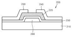
도 2는 본 발명의 일 실시예에 따른 역 스테거드형(inverted staggered type) 박막 트랜지스터(200)를 도시하는 단면도이다. 역 스테거드형 박막 트랜지스터(200)는 기판 상에 게이트 전극과 채널층이 순차적으로 형성된 구조를 의미하며, 바텀-게이트(Bottom-Gate) 구조 트랜지스터로 지칭될 수 있다.2 is a cross-sectional view illustrating an inverted staggered type
도 2를 참조하면, 역 스테거드형 박막 트랜지스터(200)는 기판(210) 상에 순차적으로 위치한 게이트 전극(260)과 게이트 절연층(250), 게이트 절연층(250) 상에 위치한 채널층(220), 및 채널층(220)의 양 단부에 각각 위치한 소스 전극(230)과 드레인 전극(240)을 포함한다.2, an inverted staggered
기판(210), 채널층(220), 소스 전극(230), 드레인 전극(240), 게이트 절연층(250), 및 게이트 전극(260)의 기능과 구성 물질은 도 1을 참조하여 상술한 기판(110), 채널층(120), 소스 전극(130), 드레인 전극(140), 게이트 절연층(150), 및 게이트 전극(160)과 동일하거나 유사할 수 있다. 그러므로, 이하에서는 기판(210), 채널층(220), 소스 전극(230), 드레인 전극(240), 게이트 절연층(250), 및 게이트 전극(260)에 대하여, 도 1을 참조하여 설명된 특징들과 동일하거나 유사한 특징들에 대한 설명은 생략하기로 한다.The functions and constituent materials of the
게이트 전극(260)은 기판(210)의 일부 영역 상에 위치할 수 있다.The
게이트 절연층(250)은 게이트 전극(260) 상에 위치할 수 있다. 게이트 절연층(250)은 게이트 전극(260)을 덮도록 위치할 수 있고, 기판(210) 상으로 연장될 수 있다.The
채널층(220)은 게이트 전극(260) 상에 위치하는 게이트 절연층(250) 상에 위치할 수 있다. 예를 들어, 게이트 절연층(250)은 채널층(220)과 게이트 전극(260) 사이에 개재될 수 있다.The
채널층(220)은 전체적으로 비정질 상(amorphous phase)을 가지거나, 적어도 부분적으로 비정질 상을 가지는 산화물 반도체 물질을 포함할 수 있다. 채널층(120)은 인듐-갈륨-아연-산화물(In-Ga-Zn-O, IGZO), 인듐-주석-아연-산화물(In-Sn-Zn-O, ISZO), 인듐-알루미늄-아연-산화물(In-Al-Zn-O, IAZO), 주석-알루미늄-아연-산화물(Sn-Al-Zn-O, SAZO), 및 주석-아연-산화물(Sn-Zn-O, SZO) 중의 적어도 어느 하나를 포함할 수 있다.The
또한, 채널층(220)은 안정화 첨가물을 포함할 수 있다. 상기 안정화 첨가물은 상기 등의 산화물 반도체 물질 내에 포함된 산소와 spσ와 spσ* 혼성전자궤도를 형성하여, 광 또는 전기장에 의하여 야기되는 불안정성을 방지할 수 있다. 상기 안정화 첨가물은, 론-페어(lone-pair) s-궤도를 가질 수 있다. 상기 안정화 첨가물은, 예를 들어 안티몬(Sb), 비스무트(Bi), 납(Pb), 및 주석(Sn) 중 적어도 어느 하나를 포함할 수 있다. 채널층(220)에 대하여는 하기에 상세하게 설명하기로 한다.In addition, the
소스 전극(230)과 드레인 전극(240)은 서로 분리되어 채널층(220) 상에 위치할 수 있고, 또한 기판(210) 상에 위치하도록 연장될 수 있다. 소스 전극(230)과 드레인 전극(240)은 각각 채널층(220)의 양단부 상에 위치할 수 있고, 채널층(220)과 전기적으로 및/또는 물리적으로 연결될 수 있다.
The
비정질 산화물 반도체 물질의 특성Properties of amorphous oxide semiconductor materials
본 발명은 높은 전하 이동성을 가지는 비정질 산화물 반도체 층에 관한 것으로서, 상기 비정질 산화물 반도체 층은, 예를 들어 박막 트랜지스터의 채널층에 응용될 수 있다.The present invention relates to an amorphous oxide semiconductor layer having high charge mobility, and the amorphous oxide semiconductor layer can be applied to, for example, a channel layer of a thin film transistor.
상기 비정질(amorphous) 산화물 반도체 층을 구성하는 비정질 산화물 반도체 물질은, 예를 들어 인듐-갈륨-아연-산화물(In-Ga-Zn-O, IGZO), 인듐-주석-아연-산화물(In-Sn-Zn-O, ISZO), 인듐-알루미늄-아연-산화물(In-Al-Zn-O, IAZO), 주석-알루미늄-아연-산화물(Sn-Al-Zn-O, SAZO), 주석-아연-산화물(Sn-Zn-O, SZO) 등이 알려져 있다.The amorphous oxide semiconductor material constituting the amorphous oxide semiconductor layer may be an amorphous oxide semiconductor material such as indium-gallium-zinc-oxide (IGZO), indium-tin-zinc oxide Zn-O, ISZO), indium-aluminum-zinc-oxide (In-Al-Zn-O, IAZO), tin- Oxide (Sn-Zn-O, SZO) and the like are known.
이하에서는, 비정질 산화물 반도체 물질의 일 예로서, 비정질 인듐-갈륨-아연-산화물(In-Ga-Zn-O, IGZO)에 대하여 설명하기로 한다. 그러나, 본 발명의 기술적 사상에 비정질 인듐-갈륨-아연-산화물에 한정되는 것은 아니다.Hereinafter, amorphous indium-gallium-zinc-oxide (In-Ga-Zn-O, IGZO) will be described as an example of the amorphous oxide semiconductor material. However, the technical idea of the present invention is not limited to the amorphous indium-gallium-zinc-oxide.
인듐-갈륨-아연-산화물(In-Ga-Zn-O, IGZO)은 인듐 산화물(In2O3), 갈륨 산화물(Ga2O3) 및 아연 산화물(ZnO)을 기초로 구성된 InGaZnO4 일 수 있다. 이하에서는 비정질 인듐-갈륨-아연-산화물을 "a-IGZO"로 지칭하기로 한다.Indium-gallium-zinc-oxide (In-Ga-ZnO, IGZO ) is indium oxide (In2 O3), gallium oxide (Ga2 O3) and zinc oxide (ZnO) can be configured on the basis of InGaZnO4 il have. Hereinafter, the amorphous indium-gallium-zinc-oxide will be referred to as "a-IGZO".
상기 a-IGZO의 특징들 중 하나는 비정질상(amorphous phase)에서 기인하는 무질서와 휘어짐의 특성들을 가짐과 동시에 결정상(crystal phase)과 비교할 수 있는 높은 전하 이동성을 가지는 것이다. 이러한 높은 전하 이동성은 a-IGZO를 박막 트랜지스터의 채널층으로 사용할 수 있다. 이러한 a-IGZO의 높은 전하 이동성은 상기 a-IGZO를 구성하는 양이온들에 의하여 주로 형성되는 전도대(conduction bands)의 특성에 기인된다. 예를 들어, 비정질 실리콘(Si)의 경우에는, 비정질상의 구조적 무질서에 의해서 전도대 근처에 무질서 결함(disorder defect)들이 형성되며, 이에 따라 결정상과는 다른 물성을 가지게 된다. 반면, a-IGZO와 같이 IIB족 또는 IIIB족과 같은 후 전이 금속(post-transition metal)의 양이온들을 포함하는 비정질 산화물 반도체 물질의 경우에는, 상기 후 전이 금속의 양이온들은 방향성이 없고 궤도 반경이 큰 s-궤도(s-orbit)로 전도대가 주로 이루어져 있으므로, 양이온들이 무질서하게 배열되거나 물체가 휘어지더라도 s-궤도들 사이의 혼성전자궤도는 유지될 수 있고, 이에 따라 전도대는 비정질상에 의한 영향을 거의 받지 않는다. 결과적으로, 상기 후 전이 금속의 전도대의 s-궤도에 의하여, a-IGZO는 결정상과 비교할 수 있는 전하 이동성을 가질 수 있다.One of the characteristics of the a-IGZO is that it has disorder and deflection characteristics due to an amorphous phase and has a high charge mobility comparable to a crystal phase. This high charge mobility can use a-IGZO as a channel layer of a thin film transistor. The high charge mobility of a-IGZO is attributed to the characteristics of conduction bands mainly formed by the cations constituting the a-IGZO. For example, in the case of amorphous silicon (Si), disordered defects are formed near the conduction band due to the structural disorder of the amorphous phase, and thus have physical properties different from those of the crystalline phase. On the other hand, in the case of an amorphous oxide semiconductor material containing cations of post-transition metal such as Group IIB or Group IIIB, such as a-IGZO, the cations of the post-transition metal are not directional and have a large orbital radius Since the conduction band is mainly composed of s-orbit, the hybrid electron orbit between the s-orbits can be maintained even if the cations are disorderly arranged or the object is warped, and thus the conduction band is affected by the amorphous phase I hardly receive it. Consequently, due to the s-orbit of the conduction band of the post-transition metal, a-IGZO can have charge mobility comparable to the crystalline phase.
상기 a-IGZO의 양이온들 중에, 인듐은 자신의 s-궤도가 주로 전하 이동성(즉, 전기 전도도)에 영향을 줄 수 있고, 갈륨은 a-IGZO의 안정성을 증가시키고 전하 농도를 감소시킬 수 있다. 따라서, 비정질 산화물 반도체 물질의 특성은 양이온 성분들의 적절한 조합에 의하여 다양하게 변화시킬 수 있다.Of the cations of a-IGZO, indium may have its s-orbit mainly affect charge transport (i.e., electrical conductivity), gallium may increase the stability of a-IGZO and decrease the charge concentration . Thus, the properties of the amorphous oxide semiconductor material can be varied in various ways by appropriate combination of cationic components.
상기 a-IGZO와 같은 비정질 산화물 반도체 물질을 채널층으로 구성하는 박막 트랜지스터는, 낮은 온도에서 제조가 가능하고, 제조 온도를 넓게 변화시킬 수 있고, 구동 전압이 낮고, 게이트 절연체로서 다양한 물질을 사용할 수 있고, 균일성이 우수한 장점이 있다.
A thin film transistor comprising an amorphous oxide semiconductor material such as a-IGZO as a channel layer can be manufactured at a low temperature, can change a manufacturing temperature widely, has a low driving voltage, and can use various materials as a gate insulator And has excellent uniformity.
비정질 산화물 반도체의 박막 트랜지스터로의 응용 한계Application Limit of Amorphous Oxide Semiconductor to Thin Film Transistor
그러나, 비정질 산화물 반도체 물질을 박막 트랜지스터의 채널층으로 구성하는 경우에, 상기 박막 트랜지스터는 NBIS (negative bias illumination stress) 또는 IS (illumination stress)에 의한 불안정성을 가지는 한계가 있다. 이러한 불안정성은 박막 트랜지스터가 동작하는 동안에, 채널층에 인가되는 광(light) 및/또는 전기장(electric field)에 의해서 박막 트랜지스터의 전류-전압 곡선이 원하지 않게 심각하게 변화하는 것이며, 일반적으로 전류가 증가한다. 상기 불안정성은 광과 음극 전기장에 동시에 노출 되었을 때 현저하게 나타나며, 광의 세기, 광의 에너지 크기, 및 비정질 산화물 반도체 물질의 두께가 증가함에 따라, 상기 불안정성은 더욱 증가되며, 이러한 경향은 실험적으로 증명할 수 있다. 상기 불안정성의 회복 시간(즉, 상기 불안정성이 제거될 때까지 걸리는 시간)은 매우 다양하게 측정되며, 즉시 회복되는 단기적 불안정성과 1일(day) 이상의 회복 시간이 소요되는 상대적으로 영구적인 불안정성 등으로 다양하게 나타난다.However, when the amorphous oxide semiconductor material is constituted by a channel layer of a thin film transistor, the thin film transistor has a limit of instability due to negative bias illumination stress (NBIS) or illumination stress (IS). This instability is undesirably and seriously changing the current-voltage curve of the thin film transistor due to the light and / or electric field applied to the channel layer during the operation of the thin film transistor, do. The instability is conspicuous when exposed to light and cathode electric fields at the same time. As the intensity of light, the size of energy of light, and the thickness of amorphous oxide semiconductor material increase, the instability is further increased, and this tendency can be proved experimentally . The recovery time of the instability (ie, the time it takes for the instability to be removed) is measured in a wide variety of ways, including short-term instability that is recovering immediately and relatively permanent instability that requires more than one day's recovery time .
이러한 불안정성은 비정질 산화물 반도체 물질을 채널층으로서 구성하는 박막 트랜지스터의 특성을 원하지 않게 변화시키므로, 박막 트랜지스터의 실제적인 응용을 매우 어렵게 한다. 따라서, 상기 불안정성을 제거하거나 또는 적어도 감소시키는 기술이 비정질 산화물 물질로 구성된 박막 트랜지스터의 응용에 우선적 과제일 수 있다.This instability undesirably changes the characteristics of the thin film transistor constituting the amorphous oxide semiconductor material as a channel layer, making practical application of the thin film transistor very difficult. Thus, the technique of eliminating or at least reducing the instability may be a priority for application of thin film transistors composed of an amorphous oxide material.
상술한 비정질 산화물 반도체 물질의 불안정성에 대한 많은 이론적 연구들과 및 실험적 연구들이 수행되었음에도 불구하고, 상기 불안정성에 대한 메커니즘을 아직 완전하게 설명하지 못하고 있는 실정이다. 현재까지 제시된 상기 불안정성에 대한 메커니즘들 중에, 첫 번째 메커니즘은, NBIS 혹은 IS에 의하여 들뜬 정공(hole)들이 a-IGZO 활성층(즉, 채널층)에 대하여, 박막 트랜지스터의 게이트 절연체의 내부에 포획되거나 및/또는 게이트 절연체와 a-IGZO의 활성층 사이의 계면에 포획되고, 이러한 포획에 의하여 상기 정공의 탈착이 어렵게 되고, 이에 따라 불안정성이 발생한다는 것이다. 두 번째 메커니즘은, 외부에 노출된 a-IGZO 층의 표면에 산소가 흡착되거나 탈착되어 불안정성이 발생한다는 것이다. 이러한 첫 번째 및 두 번째 메커니즘들은 외부적 요인에 의한 불안정성으로 분류될 수 있다.Although there have been many theoretical and experimental studies on the instability of the amorphous oxide semiconductor material described above, the mechanism for such instability has not yet been fully described. Of the mechanisms for instability presented so far, the first mechanism is that the holes excited by NBIS or IS are trapped in the gate insulator of the thin film transistor with respect to the a-IGZO active layer (i.e., channel layer) And / or trapped at the interface between the gate insulator and the active layer of a-IGZO, and the trapping of the holes becomes difficult due to the trapping, thereby causing instability. The second mechanism is that oxygen is adsorbed or desorbed on the surface of the a-IGZO layer exposed to the outside, resulting in instability. These first and second mechanisms can be classified as external instability instability.
반면, 상기 외부적 요인에 의한 불안정성이 존재하지만, 박막 트랜지스터 외의 구조 내에 포함된 비정질 산화물 반도체 물질 박막에서도 불안정성이 발생하는 점과, 불안정성이 비정질 산화물 반도체 물질의 두께에 의존하는 점을 고려하면, 비정질 산화물 반도체 물질 자체의 내부적 요인에 의한 불안정성도 존재한다고 예상할 수 있다.On the other hand, considering the instability due to the external factors, but also the instability in the amorphous oxide semiconductor material thin film included in the structure other than the thin film transistor and the fact that the instability depends on the thickness of the amorphous oxide semiconductor material, It is expected that there is instability due to the internal factors of the oxide semiconductor material itself.
세 번째 메커니즘에 따르면, 아연 산화물에서의 산소 결함(VO)의 거동과 유사하게, a-IGZO 내에서의 산소 결함도 전하 상태에 따라 다른 결함 에너지 준위를 가지며, 이에 따라 비정질 산화물 반도체 물질이 불안정성을 가진다는 것이다. 예를 들어, VO+2는 얕은 에너지 준위를 가질 수 있고, VO0는 깊은 에너지 준위를 가질 수 있다. 그러나, 산소 결함에 기반한 메커니즘은 상기 불안정성이 가시광선 영역과 자외선 영역에서 다르게 측정되고, 0.9 eV까지의 큰 회복 활성화 에너지 장벽이 측정되는 것을 명확하게 설명하지 못하는 한계가 있다.According to a third mechanism, similar to the behavior of oxygen vacancies (V0 ) in zinc oxide, the oxygen vacancies in a-IGZO also have different defect energy levels depending on the charge state, and thus the amorphous oxide semiconductor material is unstable . For example, VO+2 may have a shallow energy level and VO0 may have a deep energy level. However, mechanisms based on oxygen defects have limitations in that the instability is measured differently in the visible and ultraviolet regions and does not clearly account for the large recovery activation energy barriers up to 0.9 eV.
상술한 바와 같은 세 가지 메커니즘들을 기반으로, 비정질 산화물 반도체 물질의 불안정성을 제거하기 위하여 다양한 시도들이 수행되었다. 상술한 첫 번째 및 두 번째 메커니즘에 의한 불안정성을 제거하기 위해서, 게이트 절연체에 차단층(blocking layer) 삽입하거나 또는 박막 트랜지스터 상에 패시베이션 층(passivation layer)을 형성하는 시도가 있었다. 상술한 세 번째 메커니즘에 의한 불안정성을 제거하기 위해서, 산소 결함의 감소를 위하여 산소와 강하게 결합하는 지르코늄 또는 하프늄을 도핑하거나 산소 기체의 압력을 조절함으로써 산소 결함의 농도를 감소시키려는 시도가 있었다. 그러나, 이러한 시도들은 극히 제한적인 불안정성을 제거하는 것으로 나타났다. 따라서, 상술한 메커니즘 이외에 불안정성에 대한 다른 주요한 메커니즘이 존재할 것으로 예상할 수 있다. 본 발명의 기술적 특징은 비정질 산화물 반도체 물질의 불안정성에 대한 메커니즘과 이에 대한 해결방안을 제시함으로써, 광과 전기장 스트레스에 강하고 안정적인 비정질 산화물 반도체 물질을 제공하고, 또한 상기 비정질 산화물 반도체 물질을 채널 영역으로 사용함으로써 높은 전하 이동성과 함께 신뢰성있는 박막 트랜지스터를 제공하는 것이다.
Based on the three mechanisms as described above, various attempts have been made to eliminate the instability of the amorphous oxide semiconductor material. In order to eliminate instability caused by the first and second mechanisms described above, there has been an attempt to insert a blocking layer into the gate insulator or to form a passivation layer on the thin film transistor. Attempts have been made to reduce the concentration of oxygen defects by doping zirconium or hafnium which strongly binds to oxygen or by controlling the pressure of oxygen gas in order to reduce the oxygen deficiency. However, these attempts have shown to eliminate extremely limited instability. Thus, it can be expected that there will be other major mechanisms for instability besides the mechanisms described above. A technical feature of the present invention is to provide a mechanism for instability of amorphous oxide semiconductor material and a solution thereto, thereby providing amorphous oxide semiconductor material which is strong and stable against light and electric field stress, and also uses the amorphous oxide semiconductor material as a channel region Thereby providing a reliable thin film transistor with high charge mobility.
본 발명에 따른 이론적 계산 방법The theoretical calculation method according to the present invention
본 발명에서는 비정질 산화물 반도체 물질의 불안정성의 원인을 분석하고, 안티몬과 같은 첨가 원소를 첨가함으로써 광 및 전기장 스트레스에 안정적인 비정질 산화물 반도체 물질을 구현하는 방법을 이론적 계산 결과를 통하여 제시하고자 한다.In the present invention, the cause of instability of an amorphous oxide semiconductor material is analyzed and a method of realizing an amorphous oxide semiconductor material stable to light and electric field stress by adding an additive element such as antimony is presented through the theoretical calculation results.
본 발명을 위한 이론적 계산은 PAW(Projector Augmented Wave) 슈도 포텐셀 (pseudopotentials)을 기반으로 하는 VASP (Vienna Ab Initio Simulation Package) 프로그램을 사용해서 제일 원리 계산(first-principles calculations)을 수행하여 제공하였다.Theoretical calculations for the present invention were performed by performing first-principles calculations using a Vienna Ab Initio Simulation Package (VASP) program based on Projector Augmented Wave (PAW) pseudopotentials.
비정질 산화물 반도체 물질인 a-IGZO에 안티몬(Sb)이 첨가된 다양한 조합들에 대한 비정질상 원자구조들을 구하기 위해, 마름모 형태의 슈퍼셀(supercell)을 사용해서 노제 정준 앙상블(Nose canonical ensemble)을 기반으로 한 융해-및-급냉(melt-and-quench) 분자 동역학(molecular dynamics, MD)을 PBE(Perdew-Burke-Ernzerhof)를 사용하였다. 또한, 분자 동역학의 결과적인 구조를 이용하여, DFT(density-functional-theory) 정 계산을 반복적으로 수행하여 전체 에너지가 안정화되는 것을 최종 구조로 선택하였다. 계산에 있어서, a-IGZO의 밴드갭(band-gap)이 매우 작게 계산되므로, "PBE+U" 계산(In, Ga, 및 Zn의 d의 U는 5 eV임)을 주로 사용하였다. 또한, 결과에 대해서 HSE (Heyd-Scuseria-Ernzerhof) 계산을 사용하여 검증하였다. 상기 HSE 계산에서는, Hartree-Fock를 25% 섞고, 스크린 파라미터(screening parameter)는 0.2 Å-1로 고정하였다.
In order to obtain amorphous atomic structures for various combinations of antimony (Sb) added to a-IGZO, amorphous oxide semiconductor material, a rhombic supercell is used based on a Nose canonical ensemble A melt-and-quench molecular dynamics (MD) was used as a PBE (Perdew-Burke-Ernzerhof). In addition, the final structure was selected by using DFT (density-functional-theory) calculations repeatedly using the resulting structure of molecular dynamics to stabilize the total energy. In calculation, the band-gap of a-IGZO is calculated to be very small, so the calculation of "PBE + U" (U of d of In, Ga and Zn is 5 eV) is mainly used. The results were also verified using HSE (Heyd-Scuseria-Ernzerhof) calculations. In the HSE calculation, Hartree-Fock was mixed at 25% and the screening parameter was fixed at 0.2 A-1 .
비정질 산화물 반도체 물질의 불안정성에 대한 새로운 메커니즘 검토A new mechanism for the instability of amorphous oxide semiconductor materials
도 3 및 도 4은 안정화 첨가물을 포함하지 않은 경우의 비정질 산화물 반도체 물질의 불안정성의 원인을 설명하기 위한 도면들이다.FIGS. 3 and 4 are diagrams for explaining the cause of the instability of the amorphous oxide semiconductor material when the stabilizing additive is not included.
비정질 산화물 반도체 물질의 불안정성의 원인을 규명하기 위하여, 비정질 상에 존재하는 무질서 결함(disorder defect)을 고려하기로 한다. 상술한 바와 같이, 비정질 산화물 반도체 물질의 전도대(conduction band, CB)에서는 상기 무질서 결함에 의한 변화가 없거나 크지 않므로, 높은 전하이동성을 유지할 수 있다. 반면 상기 비정질 산화물 반도체 물질의 원자가 전자대(valence band, VB)에서는, 비정질 실리콘과 유사하게, 상기 무질서 결함에 의한 변화가 발생할 수 있다. 그 이유는, 상기 비정질 산화물 반도체 물질의 전도대는 방향성이 없는 s-궤도로 구성되는 반면, 상기 비정질 산화물 반도체 물질의 원자가 전자대는 방향성을 가지는 산소의 2p-궤도로 주로 이루어져 있기 때문이다.In order to clarify the cause of the instability of the amorphous oxide semiconductor material, a disorder defect existing in the amorphous phase will be considered. As described above, the conduction band (CB) of the amorphous oxide semiconductor material has no or little change due to disordered defects, so that high charge mobility can be maintained. On the other hand, in the valence band (VB) of the amorphous oxide semiconductor material, a change due to the disordered defect may occur similarly to the amorphous silicon. This is because the conduction band of the amorphous oxide semiconductor material is composed of an unoriented s-orbit while the valence electron band of the amorphous oxide semiconductor material is mainly composed of a 2p-orbit of oxygen having a directivity.
도 3를 참조하면, 상기 비정질 산화물 반도체 물질의 원자가 전자대는 무질서 결함에 의하여 최대 원자가 전자대(VB maximum, VBM)에서 약 0.4 eV 내지 약 0.8 eV 정도의 폭으로 퍼지는 원자가 전자대 꼬리(VB tail, VBT)를 밴드 갭(band gap) 내에 형성한다. 이러한 상태를 무질서 결함 상태(Disorder state, DS)로 지칭하기로 한다. 상기 무질서 결함 상태는 광 및/또는 전기장에 의해서 들뜬 정공들이 상호작용할 수 있고, 산소-산소 결합 상태를 변화시킬 수 있다.Referring to FIG. 3, the valence electron band of the amorphous oxide semiconductor material has a valence electron tail (VB tail) spreading at a width of about 0.4 eV to about 0.8 eV at a maximum VBM by disorderless defects, VBT are formed within a band gap. This state will be referred to as a disordered state (DS). In the disordered defect state, holes excited by light and / or electric field can interact and change the oxygen-oxygen bonding state.
상기 원자가 전자대 꼬리는 상기 비정질 산화물 반도체 물질에 포함된 두 개의 산소들 사이의 ppσ 혼성전자궤도 형성에 의하여 만들어진 ppσ* 혼성전자궤도에 의해서 형성될 수 있다. 상기 두 개의 산소들 사이의 결합은 산소들 사이의 거리를 가깝게 하는 "결합(bonding)"과 산소들 사이의 거리를 멀게 하는 "반결합(anti-bonding)"의 개념으로 설명할 수 있다. 정공이 포획되지 않은 원자가 전자대 꼬리는 상기 결합과 상기 반결합이 동시에 영향을 미치므로, 적정한 산소 원자 사이의 거리에서 ppσ와 ppσ* 혼성전자궤도를 모두 형성할 수 있다. 이때의 ppσ혼성전자궤도는 ppσ* 혼성전자궤도의 영향으로 상대적으로 약한(weak) 결합 상태를 나타낸다.The valence electron tail can be formed by a ppσ * hybrid electron orbit formed by the formation of a ppΣ hybrid electron orbit between two oxygen atoms contained in the amorphous oxide semiconductor material. The bond between the two oxygens can be explained by the concept of "bonding," which brings the distance between the oxygenes closer together, and "anti-bonding," which makes the distance between the oxygenes away. The valence electron tail of the electron without trapping holes can simultaneously form both ppσ and ppσ * hybrid electron orbitals at a distance between the proper oxygen atoms because the bond and the half-bond simultaneously affect each other. At this time, the ppσ hybrid electron orbit exhibits a relatively weak (weak) coupling state due to the influence of ppσ * hybrid electron orbit.
도 4를 참조하면, 광 및/또는 전기장에 의해서 생성된 두 개의 정공이 원자가 전자대 꼬리 내에 포획되면, 전자들은 결합(bonding)에만 관여하게 되므로, 두 개의 산소들 사이의 거리가 가까워지면서 ppσ 혼성전자궤도가 형성되며, 이때의 ppσ 혼성전자궤도는 상대적으로 강한(strong) 결합 상태를 나타낸다.Referring to FIG. 4, when two holes generated by light and / or electric field are trapped in a valence electron-to-tail, electrons are only involved in bonding, so that the distance between two oxygen becomes close to each other, The electron orbit is formed, and the ppΣ hybrid electron orbit exhibits a relatively strong bonding state.
상기 강한 ppσ 혼성전자궤도는 원자가 전자대 내에서 에너지적으로 안정화되면서, 전자가 채워지지 않은(즉, 정공을 포함하는) ppσ* 혼성전자궤도의 에너지 준위를 전도대로 올라가게 한다. 즉, 정공에 의하여 산소들은 (O2-+O2-+2h)+2e -> O22-+2e (여기에서, e는 전자이고, h는 정공임) 반응을 발생시키고, 결과적으로 두 개의 전자(2e)를 제공하는 도너(donor)로써 전자 농도를 증가시키게 된다. 정공을 포함하여 형성된 산소-산소 결합 구조는 무질서 결함 상태(DS)에 비하여 약 1.0 eV 정도로 에너지적으로 안정하게 되며, 이는 도 4에 ppσ 에너지 준위의 "δE" 만큼 깊어짐에 따라 산소-산소 결합 구조의 전체 에너지가 안정화될 수 있다. 상기 O22-는 과산화물(peroxide)이며, 이러한 상태를 과산화물 상태(peroxide state, PS)로 지칭하기로 한다.The strong ppσ hybrid electron orbit causes the energy level of the ppσ * hybrid electron orbit that is not filled with electrons (ie, contains holes) to rise to the conduction band, while being stabilized energetically in the valence electron band. That is, the holes cause the oxygen (O2 + O2- + 2h) + 2e -> O22- + 2e (where e is the electron and h is the hole) Donor donor to provide electrons 2e. The oxygen-oxygen bond structure formed including holes is energetically stable to about 1.0 eV as compared to the disordered defect state (DS), and this becomes more stable as the "? E " Can be stabilized. The O22- is peroxide, and this state is referred to as a peroxide state (PS).
비정질 산화물 반도체 물질의 불안정성은 상술한 바와 같은 정공 및 전자의 결합에 의하여 발생하는 무질서 결함 상태(DS)와 과산화물 상태(PS) 사이의 구조적인 전이로 이해 될 수 있다.The instability of the amorphous oxide semiconductor material can be understood as a structural transition between the disordered defect state (DS) and the peroxide state (PS), which is caused by the combination of holes and electrons as described above.
도 5는 안정화 첨가물을 포함하지 않은 경우의 비정질 산화물 반도체 물질의 원자 결합 상태에 따른 에너지 변화를 나타내는 그래프이다. 도 6은 도 5의 각 상태에 대한 원자들의 결합을 나타내는 모식도들이다.FIG. 5 is a graph showing an energy change according to an atomic bonding state of an amorphous oxide semiconductor material when the stabilizing additive is not included. FIG. 6 is a schematic diagram showing the combination of atoms for each state in FIG. 5; FIG.
도 5를 참조하면, 적색 선은 들뜬 무질서 결함 상태(DS*)로부터 들뜬 과산화물 상태(PS*)로의 전이 시의 에너지 변화를 나타내고, 청색 선은 안정 과산화물 상태(PS)로부터 안정 무질서 결함 상태(DS)로의 전이 시(즉, 회복을 나타냄)의 에너지 변화를 나타낸다. 상기 에너지 변화는 산소-산소 거리에 따라 변화한다. 전이 상태(transition state, TS)는 전이시의 최대 에너지 값을 가지는 상태로서, 상태 전이시의 활성 에너지 장벽(activation energy barrier)과 관련된다. "TS*"는 들뜬 전이 상태를 나타내고, "TS"는 안정 전이 상태를 나타낸다. 들뜬 경우에는 "+2"의 전하 상태를 가질 수 있고, 안정된 경우에는 "0"의 전하 상태를 가질 수 있다.5, the red line represents the energy change at transition from the excited disordered state DS * to the excited peroxide state PS *, and the blue line represents the stable disordered state PS from the stable disordered state DS (I. E., Recovery). ≪ / RTI > The energy change varies with the oxygen-oxygen distance. The transition state (TS) is the state having the maximum energy value at the transition and is related to the activation energy barrier at the state transition. "TS *" indicates an excited transition state, and "TS" indicates a stable transition state. Quot; + 2 "in the case of excitation, and a charge state of" 0 " in the case of stable.
도 6을 참조하면, 각 상태의 원자들의 결합을 도시하고 있으며, 적색 구체가 산소를 나타낸다. 무질서 결함 상태(DS* 또는 DS)에서는 산소-산소 결합이 나타나지 않으며, 과산화물 상태(PS*, PS) 및 전이 상태*(TS*, TS)에서는 산소-산소 결합이 나타난다.Referring to FIG. 6, the combination of atoms in each state is shown, wherein the red spheres represent oxygen. No oxygen-oxygen bonds appear in disordered states (DS * or DS), and oxygen-oxygen bonds appear in peroxide state (PS *, PS) and transition state * (TS *, TS).
들뜬 무질서 결함 상태(DS*)로부터 들뜬 과산화물 상태(PS*)로의 전이 시에, 활성 에너지 장벽(α)은 0 eV (HSE 계산의 경우임) 또는 0.26 eV (PBE+U 계산의 경우임)으로 상대적으로 작은 값의 에너지 장벽을 가질 수 있다. 반면, 안정 과산화물 상태(PS)로부터 안정 무질서 결함 상태(DS)로의 전이 시에, 활성 에너지 장벽(β)은 0.97 eV (HSE 계산의 경우임) 또는 0.69 eV (PBE+U 계산의 경우임)으로 상대적으로 큰 값의 에너지 장벽을 가질 수 있다. 여기에서, β의 0.97 eV (HSE 계산의 경우임) 값은 실험적으로 측정된 회복 에너지 장벽 (0.9 eV)과 거의 유사함을 알 수 있다.The activation energy barrier (α) is 0 eV (for HSE calculations) or 0.26 eV (for PBE + U calculations) at transition from the excited disordered state (DS *) to the excited peroxide state (PS * It can have a relatively small value of energy barrier. On the other hand, at transition from stable peroxide state (PS) to stable disordered state (DS), the active energy barrier (β) is 0.97 eV for HSE calculations or 0.69 eV for PBE + U calculations It can have a relatively large energy barrier. Here, the value of 0.97 eV (in the case of HSE calculation) of β is almost similar to the experimental recovery energy barrier (0.9 eV).
회복에 대한 에너지 장벽(β)의 크기는 전도대의 최저부(CBM)으로부터의 ppσ* 혼성 전자 궤도의 에너지 준위의 이격 거리(δ, 도 4 참조)로 나타나는 에너지 준위 차이에 의하여 결정된다. 이격 거리(δ)가 작으면, 산소-산소 결합 구조가 쉽게 전자를 포획해서 안정 무질서 결함 상태(DS)로 회복됨을 의미한다.The magnitude of the energy barrier (β) for recovery is determined by the difference in energy level between ppσ * from the lowest part of the conduction band (CBM) and the separation distance (δ, see FIG. 4) of the energy level of the hybrid electron orbit. If the separation distance? Is small, it means that the oxygen-oxygen bond structure easily captures electrons and is restored to the stable disorder defect state (DS).
결론적으로, 상술한 무질서 결함 상태가 광 및/또는 전기장에 의하여 들뜬 정공과 상호작용함으로써, 비정질 산화물 반도체 물질의 불안정성을 발생시킬 수 있음이 증명된다.
In conclusion, it has been demonstrated that the disordered defect states described above can cause instability of the amorphous oxide semiconductor material by interacting with the holes excited by light and / or electric fields.
안정화 첨가물의 첨가에 따른 비정질 산화물 반도체 물질의 안정성 향상Improve stability of amorphous oxide semiconducting materials by addition of stabilizing additive
상술한 바와 같은 비정질 산화물 반도체 물질의 광 및/또는 전기장에 의하여 발생되는 불안정성을 제거하기 위한 하나의 방법은, 원자가 전도대 꼬리의 산소-산소 ppσ* 혼성전자궤도를 변경함으로써, 원하지 않는 산소-산소 결합을 방지하는 것이다. 이를 위하여, 강유전체 PbTiO3의 Pb, 다강체 BiFeO3의 Bi, 혹은 p-형 반도체 SnO의 Sn과 같은 론-페어(lone-pair) 궤도를 가지는 양이온 물질을 고려할 수 있다.One method for eliminating the instability caused by the light and / or electric field of the amorphous oxide semiconductor material as described above is to change the oxygen-oxygen pp? * Hybrid electron trajectory of the valence conduction band tail, . For this purpose, a cationic material having a lone-pair orbit such as Pb of ferroelectric PbTiO3 , Bi of a rigid body BiFeO3 , or Sn of a p-type semiconductor SnO can be considered.
상기 론-페어 궤도를 가지는 양이온들은 완전히 채워져 있는 s-궤도를 가지고 있다. 상기 양이온들의 s-궤도와 원자가 전자대의 상호작용에 의한 특성은 산소 2p-궤도로 이루어진 물질의 경우에 의한 특성과는 다를 수 있다. 상술한 바와 같이, 비정질 산화물 반도체 물질의 원자가 전자대는 주로 산소 2p-궤도로 이루어져 있으므로, 론-페어 궤도를 가지는 양이온들을 안정화 첨가물로서 상기 비정질 산화물 반도체 물질에 첨가하면, 원자가 전자대 꼬리의 에너지 준위 상태는 론-페어 s-궤도와 산소 2p-궤도의 혼성에 의하여 변경될 수 있다.The cations having the Ron-Pair orbit have s-orbits that are completely filled. The characteristics of the interaction between the s-orbit and the valence electron band of the cations may differ from those of the material consisting of oxygen 2p-orbits. As described above, since the valence electron band of the amorphous oxide semiconductor material is mainly composed of oxygen 2p-orbitals, when cations having a Ron-pair orbit are added to the amorphous oxide semiconductor material as a stabilizing additive, the valence electron- Can be modified by the hybridization of the Ron-pair s-orbit and the oxygen 2p-orbit.
상기 안정화 첨가물로서, 론-페어 s-궤도를 가진 비스무트(Bi), Sn(주석), 납(Pb), 또는 안티몬(Sb) 등을 선택할 수 있다. 원자가 전자대 꼬리의 에너지 준위 상태를 변경하기 위하여, 안티몬(Sb) 및/또는 납(Pb)이 바람직한 안정화 첨가물일 수 있다. 비스무트(Bi)의 경우, 비스무트(Bi)의 론-페어 6s-궤도가 안티몬(Sb2O3)의 5s-궤도보다 에너지 준위가 깊기 때문에, 산소 2p-궤도와의 상호작용이 작게 되며, 따라서 원자가 전자대 꼬리의 에너지 준위 상태의 변경이 상대적으로 작을 수 있다. 주석(Sn)의 경우, SnO의 Sn2+ 가 SnO2의 Sn4+에 비하여 준안정(metastable) 상태이므로, 론-페어 s-궤도를 가진 Sn2+를 많은 농도로 제공하기 어려울 수 있다. 따라서, 이하에서는 비정질 산화물 반도체 물질, 특히 a-IGZO에 안티몬(Sb)을 첨가한 경우를 예시적으로 설명하기로 한다. 또한, 납(Pb)도 안티몬(Sb)과 유사한 효과를 제공할 수 있다. 그러나 본 발명의 기술적 사상이 이에 한정되는 것은 아니고 다른 론-페어 s-궤도를 가지는 양이온들을 첨가물로 비정질 산화물 반도체 물질에 포함하는 경우도 본 발명의 기술적 사상에 포함된다.
As the stabilizing additive, bismuth (Bi), Sn (tin), lead (Pb), or antimony (Sb) having Ron-pair s-orbit can be selected. Antimony (Sb) and / or lead (Pb) may be a preferred stabilizing additive to alter the energy level state of the valence electron-to-tail. In the case of bismuth (Bi), since the Ron-pair 6s-orbit of bismuth (Bi) has a higher energy level than the 5s-orbit of antimony (Sb2 O3 ), the interaction with oxygen 2p- The change in the energy level state of the valence electron-to-tail can be relatively small. In the case of tin (Sn), since Sn2 + of SnO2 is metastable compared to Sn4+ of SnO2 , it may be difficult to provide Sn2 + having a ron-pair s-orbit at a high concentration. Therefore, a case where antimony (Sb) is added to an amorphous oxide semiconductor material, particularly a-IGZO, will be described below as an example. In addition, lead (Pb) can also provide an effect similar to antimony (Sb). However, the technical idea of the present invention is not limited to this, and the case of incorporating cations having other Ron-pair s-orbits into an amorphous oxide semiconductor material as an additive is also included in the technical idea of the present invention.
론-페어 물질 함량에 대한 비정질 산화물 반도체 물질의 안정성 향상Improving the stability of amorphous oxide semiconductor materials to ron-pair material content
광 및/또는 전기장에 의해서 발생되는 비정질 산화물 반도체 물질의 불안정성에 대한 안티몬 첨가의 영향을 정량적으로 알아보기 위해서, a-IGZO에 안티몬을 첨가하는 경우를 예시적으로 상술한 계산방법을 이용하여 검토하였다. 안티몬은 상기 a-IGZO의 인듐(In), 갈륨(Ga), 또는 아연(Zn)의 자리를 치환하는 것으로 가정하였으며, 상기 치환에 따른 다양한 조합을 검토하였다. 이하에서는, 상기 안티몬이 첨가되어 치환된 물질을 "a-IGZO:Sb"로 지칭하기로 한다. 안티몬 산화물은 일반적으로 Sb2O3 (이경우에는 Sb+3임) 또는 Sb2O5 (이경우에는 Sb+5임)로 존재 할 수 있으며, Sb2O3이 보다 안정된 산화물이므로, 안티몬이 Sb2O3와 같은 조성비를 가지도록 산소 조성을 구성하였다. 3가 이온이 될 수 있는 인듐이나 갈륨과는 달리, 아연은 안티몬과는 다른 전하를 가지므로 첨가되는 양이 달라지게 됨을 유의한다. 따라서, 안티몬이 첨가되기 전의 a-IGZO의 총 산소 함량을 유지하도록, 원소의 성분비를 구성하였다. 구체적으로, 안티몬이 인듐을 대체하는 경우는 a-In1-xGaZnO4:Sbx (여기에서, x=1/16,1/8,1/4,3/8,1/2,3/4,1)의 7가지 경우에 대하여 검토하였고, 안티몬이 갈륨을 대체하는 경우는 a-InGa1-xZnO4:Sbx (여기에서, x=1/16,1/8,1/4,3/8,1/2,3/4,1)의 7가지 경우에 대하여 검토하였고, 안티몬이 아연을 대체하는 경우는 a-InGaZn1-3x/2O4:Sbx (여기에서, x=1/8,1/4,1/2,5/8)의 4가지 경우에 대하여 검토하였다.
In order to quantitatively investigate the effect of antimony addition on the instability of an amorphous oxide semiconductor material generated by light and / or electric field, the addition of antimony to a-IGZO was studied using the calculation method described above as an example . It is assumed that antimony displaces indium (In), gallium (Ga), or zinc (Zn) of the a-IGZO, and various combinations depending on the substitution were examined. Hereinafter, the substance to which the antimony is added and is substituted will be referred to as "a-IGZO: Sb ". Antimony oxide is usually Sb2 O3 (in this case Sb+3 Im) or Sb2 O5 because it can be present in the (in this case being Sb+5), Sb2 O3 is more stable oxide, antimony Sb2 O3 composition ratio. Note that unlike indium or gallium, which can be a trivalent ion, zinc has a different charge than antimony, so the amount added is different. Therefore, the component ratio of the elements was configured to maintain the total oxygen content of a-IGZO before adding antimony. Specifically, in the case of antimony replaces the indium isa-In 1 -x GaZnO 4: Sb x ( where, x = 1 / 16,1 / 8,1 / 4,3 / 8,1 / 2,3 / 4, 1). In the case of antimony substituting for gallium, a-InGa1-x ZnO4 : Sbx (where x = 1/16, 1/8, 1/4, 3/8, 1 / 2,3 / 4,1), and when antimony substitutes for zinc, a-InGaZn1-3x / 2O4 : Sbx (where x = 1/8, 1/4, 1 / 2,5 / 8).
비정질 산화물 반도체 물질에 안정화 첨가물의 첨가에 따른 전자 결합 메커니즘Electron bonding mechanism by addition of stabilizing additive to amorphous oxide semiconductor material
도 7 및 도 8은 안정화 첨가물로서 안티몬을 첨가한 경우의 비정질 산화물 반도체 물질의 안정성 향상을 설명하기 위한 도면들이다. 도 9는 안정화 첨가물로서 안티몬을 첨가한 경우의 비정질 산화물 반도체 물질의 원자 결합 구조와 원자가 전자대 꼬리(VBT)의 spσ*전자구조를 나타내는 모식도이다FIGS. 7 and 8 are diagrams for explaining the stability improvement of the amorphous oxide semiconductor material when antimony is added as a stabilizing additive. 9 is a graph showing the relationship between the atomic bonding structure of the amorphous oxide semiconductor material and the sp σ * of the valence electron-to-tail (VBT) when antimony is added as a stabilizing additive. Is a schematic diagram showing an electronic structure
도 7을 참조하면, 안티몬의 5s-궤도는 원자가 전자대 아래쪽에 위치하고, 최인접 산소와 약한 spσ 결합을 한다. 이에 따라, 원자가 전자대는 비정질에 의한 무질서 결합과 spσ 결합에 의하여 형성된 원자가 전자대 꼬리를 가지게 된다. 상기 원자가 전자대 꼬리는, 안티몬이 없는 경우에 비하여, 첨가된 안티몬의 농도에 비례하여 더 폭을 가질 수 있고, 예를 들어 최대 0.8 eV정도까지 더 큰 폭을 가질 수 있다. 또한, 이러한 무질서 결함 상태는 안티몬의 5s-궤도의 특성을 가질 수 있다.Referring to FIG. 7, the 5s-orbit of antimony is located below the valence electron band and has a weak sp σ bond with the nearest oxygen. As a result, the valence electron band has an atomic valence electron tail formed by amorphous bond and sp σ bond. The valence electron-to-tail can have a width that is proportional to the concentration of added antimony, for example, up to a maximum of 0.8 eV, as compared to no antimony. In addition, this disordered defect state can have the property of the 5s-orbit of antimony.
도 8을 참조하면, 광 및/또는 전기장에 의해서 생성된 두 개의 정공이 원자가 전자대 꼬리 내에 포획되면, 전자들은 결합(bonding)에만 관여하게 된다. 안티몬이 첨가되지 않는 경우에는 산소-산소 결합이 강하게 형성되는 반면, 안티몬이 첨가된 경우 정공 포획에 의한 상호작용은 안티몬과 산소 사이의 결합에 근사적으로 국한되게 되어 산소-산소 결합을 방지하게 된다. 따라서, 상술한 과산화물 상태(PS)의 형성이 억제되거나 완전히 제한될 수 있다.Referring to FIG. 8, when two holes generated by light and / or electric fields are captured in a valence electron-to-tail, electrons are only involved in bonding. When antimony is not added, the oxygen-oxygen bond is strongly formed, whereas when antimony is added, the interaction due to hole trapping is limited to the bond between antimony and oxygen to prevent oxygen-oxygen bonding . Thus, the formation of the above-described peroxide state (PS) can be suppressed or completely restricted.
구체적으로, a-IGZO:Sb에서, 들뜬 정공들이 무질서 결함 상태의 원자가 전자대 꼬리 내에 포획되면, 전자들은 결합(bonding)에만 관여하게 되므로, 안티몬과 산소 사이의 거리가 가까워지면서 강한(strong) spσ 결합이 형성된다Specifically, in a-IGZO: Sb, when excited holes are trapped in a disordered electron state, electrons are only involved in bonding, so that the distance between antimony and oxygen becomes strong, Bond is formed
상기 강한 spσ결합은 원자가 전자대 내에서 에너지적으로 안정화되면서, 전자가 채워지지 않은(즉, 정공을 포함하는) spσ* 혼성전자궤도의 에너지 준위는 전도대로 올라가게 된다. 즉, 정공에 의하여 안티몬과 산소는 (Sb3++O2-+2h)+2e -> Sb5+O2-+2e (여기에서, e는 전자이고, h는 정공임) 반응을 발생시키고, 결과적으로 두 개의 전자(2e)를 제공하는 도너(donor)로써 전자 농도를 증가시키게 된다. 이때에, 전도대의 최저부(CBM)로부터의 spσ* 혼성전자궤도의 에너지 준위의 이격 거리(δ)는 매우 작으며, 안티몬이 첨가되지 않는 경우 산소-산소 결합에 의하여 형성되는 ppσ* 혼성전자궤도의 에너지 준위의 이격 거리에 비하여 매우 작다. 이격 거리(δ)가 작다는 것은 회복을 위한 활성화 에너지 장벽이 작음을 의미한다. 따라서, 비정질 산화물 반도체 물질에 론-페어 구조를 가지는 물질, 예를 들어 안티몬을 첨가하면, 과산화물의 형성(산소-산소 결합에 의함)을 방지할 수 있고, 광 및/또는 전기장에 대한 비정질 산화물 반도체 물질의 안정성을 향상시킬 수 있다.The strong sp σ bonds are energetically stabilized within the electron bands, so that the energy level of the sp σ * hybrid electron orbit, which is not filled with electrons (ie, contains holes), rises to the conduction band. That is, the hole causes the antimony and oxygen to react (Sb3+ + O2- + 2h) + 2e -> Sb5+ O2- + 2e (where e is the electron and h is the hole) And consequently increases the electron concentration as a donor that provides two electrons 2e. At this time, the separation distance (delta) of the energy level of the sp σ * hybrid electron orbit from the lowest part (CBM) of the conduction band is very small, and when the antimony is not added, the ppσ * hybrid electron orbit Is very small compared to the separation distance of the energy level of. The small separation distance (δ) means that the activation energy barrier for recovery is small. Thus, the addition of a material having a Ron-Pair structure to the amorphous oxide semiconductor material, such as antimony, can prevent the formation of peroxides (due to oxygen-oxygen bonds) and the formation of amorphous oxide semiconductors The stability of the material can be improved.
하기에서는, 안티몬이 첨가되었을 때, 들뜬 정공을 포획하지 않은 무질서 결함 상태를 "Sb(3+)", 들뜬 정공을 포획한 후의 무질서 결함 상태를 "Sb(5+)" 로 지칭하기로 한다.Hereinafter, the disordered defect state in which excited holes are not captured when antimony is added is referred to as Sb (3+), and the disordered defect state after trapping excited holes is referred to as Sb (5+).
도 9를 참조하면, 안티몬이 첨가된 a-IGZO는 Sb(3+) 상태에서 원자가 전자대 꼬리(top VBT)는 주로 안티몬의 5s-궤도의 특성을 가질 수 있다. 이는 안티몬을 중심으로 형성된 황색 원에 의하여 나타난다.
Referring to FIG. 9, the a-IGZO added with antimony can have the property of the 5s-orbit of the antimony mainly in the valence electron-to-tail (top VBT) in the Sb (3+) state. This is due to the yellow circle formed around antimony.
안정화 첨가물의 첨가에 따른 비정질 산화물 반도체 물질의 안정성 강화에 대한 에너지적 검토An Energy Review for Enhancing the Stability of Amorphous Oxide Semiconductor Materials with Addition of Stabilizing Additives
먼저, 비정질 산화물 반도체 물질에 론-페어 물질의 첨가함에 따른 과산화물 상태(PS) 형성의 변화를 정량적으로 검토하기로 한다. 수학식 1에 나타난 바와 같이, "+2"의 전하 상태인 DS2+에서, 무질서 결함 상태(DS2+)와 과산화물 상태(PS2+)에 대한 에너지 차이에 의하여 안정화 에너지(Es)를 계산할 수 있다.First, quantitative changes in the formation of peroxide state (PS) due to the addition of Ron-Pair materials to an amorphous oxide semiconductor material will be discussed. The stabilization energy Es is calculated by the energy difference between the disordered state (DS2+ ) and the peroxide state (PS2+ ) in DS2+ , which is the state of charge of "+2" .

상기 안티몬이 상기 a-IGZO의 인듐을 대체하는 경우, 상기 과산화물 상태의 안정화 에너지는 2.84 eV로 계산된다. 상기 안티몬이 상기 a-IGZO의 갈륨을 대체하는 경우, 상기 과산화물 상태의 안정화 에너지는 2.45 eV로 계산된다. 또한 상기 안티몬이 상기 a-IGZO의 아연을 대체하는 경우, 상기 과산화물 상태의 안정화 에너지는 2.04 eV로 계산된다. 상기 안정화 에너지들은 양의 값이므로, 과산화물 상태(PS2+)가 무질서 결함 상태(DS2+)에 비하여 큰 에너지를 가지므로, 과산화물 상태(PS2+)가 에너지적으로 불안정함을 나타낸다. 결론적으로, 비정질 산화물 반도체 물질에 안티몬과 같은 론-페어 물질을 첨가함으로써, 과산화물 상태(PS2+)의 발생을 방지할 수 있다.
When the antimony replaces indium of the a-IGZO, the stabilization energy of the peroxide state is calculated to be 2.84 eV. When the antimony replaces gallium in the a-IGZO, the stabilization energy of the peroxide state is calculated to be 2.45 eV. When the antimony replaces zinc of the a-IGZO, the stabilization energy of the peroxide state is calculated to be 2.04 eV. The stabilization energies, so a positive value, since peroxide status (PS2+) is of a larger energy than the disordered state defect (DS2+), indicate that the peroxide status (PS2+) the instability energetically. Consequently, the addition of the Ron-Pair material such as antimony to the amorphous oxide semiconductor material can prevent the generation of the peroxide state (PS2+ ).
안정화 첨가물의 첨가에 따른 비정질 산화물 반도체 물질의 안정성 강화에 대한 이론적 고찰Theoretical Consideration on Enhancement of Stability of Amorphous Oxide Semiconductor Material by Addition of Stabilizing Additives
도 10은 안티몬이 첨가된 a-IGZO에서 안티몬 주위의 원자 구조를 예시적으로 나타내는 모식도이다. (a)는 Sb(3+)의 경우이고, (b)는 Sb(5+)의 경우이다.10 is a schematic diagram illustrating an example of the atomic structure around antimony in a-IGZO to which antimony is added. (a) is the case of Sb (3+), and (b) is the case of Sb (5+).
도 10을 참조하면, Sb(5+)의 경우가 Sb(3+) 경우에 비하여 안티몬-산소 사이의 결합 거리가 짧게 나타난다. 이는 들뜬 정공에 의하여 안티몬과 산소 사이의 결합이 강하게 발생하는 것을 의미하며, 이는 도 7 내지 도 9를 참조하여 설명한 사항과 일치한다. 상기 Sb(3+) 상태에서 정공에 의해 Sb(5+) 상태가 되며, Sb(5+) 상태에서는 SbO6 팔면체 octahedron 원자 구조를 갖는다.Referring to FIG. 10, the coupling distance between antimony and oxygen is shorter in the case of Sb (5+) than in the case of Sb (3+). This means that a strong bond between antimony and oxygen is generated by the excited holes, which is consistent with that described with reference to FIGS. 7 to 9. In the Sb (3+) state, it becomes Sb (5+) state by holes, and in the Sb (5+) state, it has an octahedron atomic structure of SbO6 octahedron.
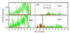
도 11은 안정화 첨가물로서 안티몬이 첨가된 비정질 산화물 반도체 물질에 대하여 에너지 준위에 따른 전자 상태 밀도를 나타내는 그래프들이다.11 is a graph showing the electron state density according to the energy level of the amorphous oxide semiconductor material to which antimony is added as a stabilizing additive.
도 11을 참조하면, Sb(3+)에서는 안티몬의 5s 궤도가 원자가 전자대 및 꼬리에 분포함을 보여주고 있다. 반면, Sb(5+)에서는 안티몬의 5s궤도가 최저부(CBM)에서부터 전도대의 최저부(CBM) 아래 영역까지 넓게 분포한다. 이에 따라 spσ* 혼성전자궤도의 에너지 준위의 이격 거리(δ)는 매우 작다는 의미이다.Referring to FIG. 11, in Sb (3+), the 5s orbit of antimony is contained in the valence electron band and the tail. On the other hand, in Sb (5+), the 5s orbit of antimony is widely distributed from the lowest part (CBM) to the lowest part of the conduction band (CBM). This means that the separation distance (δ) of the energy level of the sp σ * hybrid electron orbit is very small.
Sb(3+)에 비하여 Sb(5+)에서 전도대 내의 Sb-5s 분포가 크게 나타난다. 즉, 들뜬 정공이 원자가 전자대 꼬리 내에 포획되면, spσ 결합에 해당되는 에너지 준위까지만 전자가 채워지게 되고, 안티몬-산소 사이의 거리가 가까워지고, 이에 따라 spσ 결합은 더 강하게 된다. 따라서, Sb(5+)에서는 안티몬-산소 spσ* 혼성전자궤도의 에너지 준위가 전도대로 올라가고, 도너(donor)로 작용할 수 있다. 이는 도 7 내지 도 9를 참조하여 설명한 사항과 일치한다. 또한, spσ* 결합은 전도대 내에서 다른 결합과 잘 섞여있으며, 즉 전도대의 최저부(CBM)로부터의 spσ* 혼성전자궤도의 에너지 준위의 이격 거리(δ)가 매우 작게 나타난다. 이에 따라, 안티몬이 첨가되기 전과는 다르게 안티몬이 첨가된 비정질 산화물 반도체 물질은 활성 에너지 장벽이 거의 없다.The distribution of Sb-5s in the conduction band is larger in Sb (5+) than in Sb (3+). That is, when excited holes are trapped in the valence electron tail, only the electrons are filled up to the energy level corresponding to the sp σ bond, and the distance between the antimony and the oxygen becomes closer, and thus the sp σ bond becomes stronger. Therefore, in Sb (5+), the energy level of the antimony-oxygen sp σ * hybrid electron orbit rises to the conduction band and can act as a donor. This is consistent with what has been described with reference to Figures 7 to 9. In addition, the sp σ * bond is well mixed with other bonds in the conduction band, ie, the separation distance (δ) of the energy level of the sp σ * hybrid electron orbit from the lowest part of the conduction band (CBM) is very small. Accordingly, unlike before the addition of antimony, the amorphous oxide semiconductor material to which antimony is added has little active energy barrier.
도 12는 안정화 첨가물로서 안티몬을 첨가한 경우의 비정질 산화물 반도체 물질의 원자 결합 상태에 따른 에너지 변화를 나타내는 그래프이다.FIG. 12 is a graph showing an energy change according to an atomic bonding state of an amorphous oxide semiconductor material when antimony is added as a stabilizing additive. FIG.
도 12를 참조하면, 상술한 바와 같이, 안티몬이 첨가된 비정질 산화물 반도체 물질이 상태가 변화하여도, Sb(5+)로부터 Sb(3+)로의 회복을 위한 활성 에너지 장벽이 거의 없음을 나타낸다. 따라서, Sb(5+)로부터 Sb(3+)로의 회복이 용이할 수 있다. 이와 같이 활성 에너지 장벽이 거의 없는 것은, 안티몬의 5s-궤도와 산소의 2p-궤도의 에너지 준위의 차이가 크므로 산소-산소 결합보다는 안티몬-산소 결합이 약하게 이루어지기 때문이다. 이러한 안티몬과 산소의 상호작용은 a-IGZO:Sb의 Sb(5+)에서는 Sb(3+)에 비해서 안티몬과 주변 산소들과의 거리가 많이 짧아지게 되고 (예를 들어 0.7 Å 미만임), 근사적으로 산소 팔면체(octahedron)를 이루려는 경향성이 발생한다.
Referring to FIG. 12, as described above, the amorphous oxide semiconductor material to which antimony is added exhibits almost no active energy barrier for recovery from Sb (5+) to Sb (3+) even when the state changes. Therefore, recovery from Sb (5+) to Sb (3+) can be facilitated. The reason why there is little active energy barrier is that the antimony-oxygen bond is weaker than the oxygen-oxygen bond, because the energy level of the 2p-orbital of the 5s-orbit of the antimony differs greatly. The interaction between antimony and oxygen is much shorter (for example, less than 0.7 A) in the Sb (5+) of a-IGZO: Sb compared to Sb (3+) There is a tendency to approximate the octahedron.
안정화 첨가물의 첨가에 따른 비정질 산화물 반도체 물질의 전하 이동성 변화Change of Charge Mobility of Amorphous Oxide Semiconductor Material by Addition of Stabilizing Additives
비정질 산화물 반도체 물질에 론-페어 물질을 첨가하면, 들뜬 정공에 의한 불안정성을 방지할 수 있으나, 론-페어 물질의 첨가 자체가 전하 이동성을 감소시킬 수 있다. 따라서, 론-페어 물질의 첨가 함량이 제한될 수 있다.The addition of the Ron-Pair material to the amorphous oxide semiconductor material can prevent instability due to excited holes, but the addition of the Ron-Pair material itself can reduce charge mobility. Therefore, the addition amount of the rhone-pair material can be limited.
도 13은 비정질 산화물 반도체 물질에 안정화 첨가물로서 첨가된 안티몬 함량에 따른 전자 유효 질량의 변화를 나타내는 그래프이다.13 is a graph showing the change in electron effective mass depending on the antimony content added as a stabilizing additive to the amorphous oxide semiconductor material.
도 13을 참조하면, 전자 유효 질량(effective mass)은 전도대의 최저부(CBM)의 밴드 전자 구조로부터 계산되었으며, 안티몬의 농도가 증가됨에 따라 유효질량은 증가되었다. 이러한 증가 경향은 안티몬이 치환하는 양이온들의 종류와 무관하게 나타난다. 상기 a-IGZO:Sb의 Sb(3+) 상태에서는, 원자가 전자대는 안티몬의 론-페어 궤도와 혼성되는 반면, 전도대는 안티몬의 5p-궤도와 혼성된다. 따라서, s-궤도로 주로 구성된 전도대는 안티몬의 농도가 증가함에 따라, 전하 이동성은 감소하게 된다.Referring to FIG. 13, the effective mass was calculated from the band electron structure of the lowest part of the conduction band (CBM), and the effective mass was increased with increasing concentration of antimony. This tendency to increase is independent of the type of cations that antimony substitutes. In the Sb (3+) state of a-IGZO: Sb, the valence electron band is mixed with the Ron-Pair orbitals of antimony while the conduction band is mixed with the 5p-orbitals of antimony. Therefore, as the concentration of antimony increases, the charge mobility decreases in the conduction band mainly composed of s-orbits.
그러므로, 비정질 산화물 반도체 물질의 불안정성 방지와 전하 이동성의 감소 경향을 고려해서, 원하는 성질들을 얻기 위해서는 론-페어 구조 물질을 적절한 함량으로 비정질 산화물 반도체 물질에 첨가할 필요가 있다.Therefore, in view of the prevention of instability of the amorphous oxide semiconductor material and the tendency of decreasing the charge mobility, it is necessary to add the rhon-pair structure material to the amorphous oxide semiconductor material in an appropriate amount in order to obtain desired properties.
예를 들어, a-IGZO에 첨가되는 안티몬의 함량은 0.001 at%(원자 퍼센트) 내지 12.5 at% 범위일 수 있다. 이론적 결과에 따르면, a-IGZO에 첨가되는 안티몬의 함량이 2 at%와 4 at%에서는 전하 이동성의 감소가 거의 없었으나, 6 at% 이상에서는 전하 이동성이 현저하게 감소되었다. 이에 따라, a-IGZO에 첨가되는 안티몬의 함량은 0.001 at% 내지 6 at% 미만의 범위일 수 있다.
For example, the content of antimony added to a-IGZO may range from 0.001 at% (atomic percent) to 12.5 at%. According to the theoretical results, the decrease of the charge mobility at 2 at% and 4 at% of the a-IGZO was negligible, but the charge mobility was significantly decreased above 6 at%. Accordingly, the content of antimony added to the a-IGZO may range from 0.001 at% to less than 6 at%.
안정화 첨가물의 첨가에 따른 비정질 산화물 반도체 물질의 형성 용이성Ease of Formation of Amorphous Oxide Semiconductor Material by Addition of Stabilization Additive
도 14는 안정화 첨가물로서 안티몬이 첨가된 비정질 산화물 반도체 물질의 형성 용이성을 나타내는 그래프들이다. 비정질 산화물 반도체 물질은 a-IGZO이다. PBE의 경우와 PBE+U의 경우에 대하여 안티몬 함량에 따른 형성 엔탈피가 각각 도시되어 있다. 안티몬이 첨가되지 않은 경우는 흑색으로 표시하였고, 안티몬이 인듐을 치환하는 경우는 청색으로 표시하였고, 안티몬이 갈륨을 치환하는 경우는 적색으로 표시하였고, 안티몬이 아연을 치환하는 경우는 녹색으로 표시하였다.Fig. 14 is a graph showing the ease of formation of amorphous oxide semiconductor material to which antimony is added as a stabilizing additive. The amorphous oxide semiconductor material is a-IGZO. Formation enthalpies according to the antimony content are shown in the cases of PBE and PBE + U, respectively. In the case where antimony is not added, it is indicated in black. When antimony is replaced with indium, it is indicated in blue. When antimony is substituted with gallium, it is indicated in red, and when antimony is substituted with zinc, it is indicated as green .
a-IGZO의 형성 에너지는 총 원자수가 같은 원자를 가지는 결정 상들과 전체에너지 차이로써 정의하였고, 수학식2와 같다.The formation energy of a-IGZO is defined as the total energy difference with the crystal phases having the same atom number as the atom and is expressed by Equation (2).

(여기에서 a, b, c, 및 d는 전체에 대한 각각의 결정상의 갯수를 의미한다)(Where a, b, c, and d mean the number of individual crystal phases for the whole)
도 14를 참조하면, 안티몬이 첨가된 a-IGZO의 비정질상들의 형성 에너지는 안티몬이 없는 경우의 a-IGZO의 형성 에너지에 비해서는 대부분 낮게 나타난다. 특히, 안티몬이 인듐을 치환하는 하는 경우가 a-IGZO의 형성 에너지가 가장 낮게 나타난다. 이러한 경향은 PBE의 경우와 PBE+U의 경우에 대하여 동일하게 나타난다. 결론적으로, 안티몬이 첨가된 a-IGZO:Sb의 비정질상들은 안티몬이 첨가되지 않은 a-IGZO에 비하여 안정된 비정질 상을 형성함을 나타낸다.
Referring to FIG. 14, the formation energy of amorphous phases of a-IGZO added with antimony is much lower than that of a-IGZO without antimony. In particular, when the antimony is substituted with indium, the formation energy of a-IGZO is the lowest. This tendency is the same for PBE and PBE + U. As a result, the amorphous phase of a-IGZO: Sb with antimony added shows a stable amorphous phase compared to a-IGZO without antimony.
비정질 산화물 반도체 물질에 첨가되는 안정화 첨가물의 최소 함량 고찰Consideration of minimum content of stabilizing additive added to amorphous oxide semiconductor material
상술한 결과들은, 비정질 산화물 반도체 물질에서 나타나는 불안정성이 비정질상에 존재하는 원자배열의 무질서(disorder)에 기인한 무질서 결함에 의하여 발생할 수 있음을 증명하였고, 이러한 불안정성을 해결하기 위한 방법들 중 하나로써 안티몬과 같이 론-페어 s-궤도를 가진 양이온의 첨가를 제시하였고 이론적 계산을 통하여 타당성을 증명하였다. 상기 이론적 계산에 있어서, 계산된 안티몬의 최소 함량은 약 7.80×10²⁰/cm3 또는 그 이하로 계산될 수 있다.The above results demonstrate that the instability in the amorphous oxide semiconductor material can be caused by a disorder due to the disorder of the atomic arrangement existing in the amorphous phase. As one of the methods for solving this instability, The addition of cations with Ron-pair s-orbital as shown in Fig. In the theoretical calculation, the minimum content of calculated antimony can be calculated to be about 7.80 x 10 <20 > / cm <3 > or less.
안티몬의 실제 최소 함량은 여러 가지 방법들에 의해서 결정될 수 있다. 안티몬이 첨가된 경우에 있어서, 광 및/또는 전기장에 의해서 정공이 들뜰 때, 정공이 과산화물 상태(PS)를 형성하기 전에 안티몬에 의하여 정공이 원자가 전자대 꼬리에 포획되어 안티몬-산소 결합을 발생함으로써 불안정성이 극복될 수 있음은 상술한 바와 같다.The actual minimum content of antimony can be determined by several methods. In the case where antimony is added, holes are trapped in the valence electron-to-tail by antimony before the holes form a peroxide state (PS) when holes are introduced by light and / or electric field to generate antimony-oxygen bonds The instability can be overcome as described above.
이러한 메커니즘에는, 들뜬 정공이 무질서결함(DS)에 머무는 수명(lifetime)이 중요한 일 요소일 수 있다. 상기 정공의 수명은, "조화 전이 상태 이론(harmonic transition state theory)"를 기초로 검토하면, 과산화물 상태로의 전이에 대한 에너지 장벽에 의해서 결정될 수 있다. 도 5에서 검토한 바와 같이, 상기 에너지 장벽은 0.26 eV (PBE+U 계산의 경우임)이며, 이에 따라 들뜬 정공의 수명은 3.4 나노 초(nsec)로 계산된다.For such a mechanism, the lifetime of the excited holes in the disordered defect (DS) may be an important factor. The lifetime of the holes can be determined by the energy barrier for the transition to the peroxide state, on the basis of the "harmonic transition state theory ". As discussed in FIG. 5, the energy barrier is 0.26 eV (for PBE + U calculations) and thus the lifetime of the excited holes is calculated to be 3.4 nanoseconds (nsec).
상기 메커니즘의 다른 중요한 요소는, 상기 들뜬 정공이 안티몬에 포획되기 위한 안티몬의 에너지 준위의 실제 공간에서의 안티몬과 정공의 상호작용 영역의 크기이다. 상기 상호작용 영역을 평가하기 위해서, 상술한 최소 계산 함량의 안티몬을 포함하는 a-IGZO:Sb가 형성하는 원자가 전자대 꼬리의 파동함수(wavefunction) 분포를 통해서 정공과 안티몬의 상호작용하는 거리(R)를 결정할 수 있고, 상호작용 부피(V=4/3πR3)를 결정할 수 있다. 여기에서, 원자가 전자대의 최고부에서의 전위 밀도 분포를 계산하여 거리(R)을 결정할 수 있다.Another important element of the mechanism is the size of the interaction region of antimony and hole in the actual space of the energy level of antimony to trap the excited holes in the antimony. In order to evaluate the interaction region, the interaction distance between holes and antimony (R (R)) is calculated from the wavefunction distribution of valence electron-to-tail formed by a-IGZO: Sb containing the minimum calculated amount of antimony described above ) And determine the interaction volume (V = 4/3? R3 ). Here, the distance R can be determined by calculating the dislocation density distribution at the highest part of the valence electron band.
도 15는 안정화 첨가물로서 안티몬을 포함하는 비정질 산화물 반도체 물질에 대하여 안티몬으로부터의 거리에 따른 원자가 전자대 꼬리 (VBT) 에너지 상태를 갖는 전자의 전하밀도 분포를 나타낸 그래프이다15 is a graph showing the charge density distribution of electrons having a valence electron-to-tail (VBT) energy state according to the distance from antimony to an amorphous oxide semiconductor material containing antimony as a stabilizing additive
도 15를 참조하면, 약 1Å의 거리에서 안티몬에 의한 가장 높은 전하밀도 분포를 보이며, 약 2Å의 거리에서 산소에 의한 전하밀도 분포를 보이며, 이후 거리 증가에 따라 전하밀도 분포가 감소한다. 그러나, 약 5Å의 거리와 같이 먼 거리에서도 전하밀도 분포가 여전히 나타난다. 예를 들어, 거리(R)를 5Å로 설정하면, 안티몬의 최소 함량은 약 1.90×10²¹/cm3 이 되며, 거리(R)를 6.75Å(외삽된 거리임)로 설정하면, 안티몬의 최소 함량은 약 1.0×10²⁰/cm3으로 나타난다. 즉, 정공에 의한 과산화물(산소-산소 결합에 의한) 형성이라는 불안정성을 완전하게 억제하게 위해서는, 안티몬이 최소 농도로 대략 1.0×10²⁰/cm3 이상 첨가 또는 도핑되어야 할 것으로 예상된다. 하지만 이 보다 작은 양이라 하더라도 정공에 의한 과산화물 형성이 일부 억제될 수 있으며, 불안정성의 일부 개선이 가능할 수 있다.Referring to FIG. 15, the highest charge density distribution by the antimony is shown at a distance of about 1 A. The charge density distribution by oxygen is shown at a distance of about 2 Å, and then the charge density distribution decreases with increasing distance. However, even at distances as large as about 5 A, the charge density distribution still appears. For example, if the distance R is set to 5 ANGSTROM, the minimum content of antimony is about 1.90 x 10²¹ / cm3 , and if the distance R is set to 6.75 ANGSTROM (extrapolated distance) The content is about 1.0 × 10²⁰ / cm3 . That is, antimony is expected to be added or doped at a minimum concentration of about 1.0 x 10²⁰ / cm3 or more in order to completely suppress the instability of formation of peroxide (due to oxygen-oxygen bond) by holes. However, even smaller amounts may inhibit the formation of peroxides by holes, and some improvement in instability may be possible.
이상에서 설명한 본 발명의 기술적 사상이 전술한 실시예 및 첨부된 도면에 한정되지 않으며, 본 발명의 기술적 사상을 벗어나지 않는 범위 내에서 여러 가지 치환, 변형 및 변경이 가능하다는 것은, 본 발명의 기술적 사상이 속하는 기술분야에서 통상의 지식을 가진 자에게 있어 명백할 것이다.It will be apparent to those skilled in the art that various modifications and variations can be made in the present invention without departing from the spirit or scope of the invention as defined in the appended claims. Will be apparent to those of ordinary skill in the art.
100, 200: 박막 트랜지스터, 110, 210: 기판, 120, 220: 채널층,
130, 230: 소스 전극, 140, 240: 드레인 전극,
150, 250: 게이트 절연층, 160, 260: 게이트 전극,100, 200: thin film transistor, 110, 210: substrate, 120, 220: channel layer,
130, 230: source electrode, 140, 240: drain electrode,
150, 250: gate insulating layer, 160, 260: gate electrode,
Claims (12)
Translated fromKorean상기 비정질 산화물 반도체 층에 포함되고, 상기 산소 사이의 결합을 방지함으로써, 광 또는 전기장에 의하여 야기되는 불안정성을 방지하는 안정화 첨가물;
을 포함하고,
상기 안정화 첨가물은 론-페어(lone-pair) s-궤도를 가지고,
상기 안정화 첨가물은 상기 산소와 spσ 혼성전자궤도 및 spσ* 혼성전자궤도를 형성하고,
상기 안정화 첨가물은 안티몬(Sb), 비스무트(Bi), 및 납(Pb) 중 적어도 어느 하나를 포함하는, 박막 트랜지스터.An amorphous oxide semiconductor layer including an amorphous oxide semiconductor material containing oxygen; And
A stabilizing additive contained in the amorphous oxide semiconductor layer and preventing instability caused by light or an electric field by preventing bonding between the oxygen atoms;
/ RTI >
The stabilizing additive has a lone-pair s-orbit,
Wherein the stabilizing additive forms a sp? Hybrid electron orbit and an sp? * Hybrid electron orbit with the oxygen,
Wherein the stabilizing additive comprises at least one of antimony (Sb), bismuth (Bi), and lead (Pb).
상기 안정화 첨가물은 상기 산소에 의한 과산화물(peroxide, O22-) 형성을 방지하는, 박막 트랜지스터.The method according to claim 1,
The stabilizing additives, a thin film transistor for preventing peroxide (peroxide, O22-) formed by the oxygen.
상기 안정화 첨가물은 0.001 at% 내지 12.5 at% 범위의 함량으로 첨가되는, 박막 트랜지스터.The method according to claim 1,
Wherein the stabilizing additive is added in an amount ranging from 0.001 at% to 12.5 at%.
상기 안정화 첨가물은 0.001 at% 내지 6 at% 미만의 범위의 함량으로 첨가되는, 박막 트랜지스터.The method according to claim 1,
Wherein the stabilizing additive is added in a content ranging from 0.001 at% to less than 6 at%.
상기 안정화 첨가물의 첨가되는 최소 함량은 1.0×10²⁰/cm3 인, 박막 트랜지스터.The method according to claim 1,
Wherein the stabilizing additive has a minimum added amount of 1.0 x 10 <20 > / cm <3 & gt ;.
상기 안정화 첨가물은 3 at% 초과 내지 6 at% 미만의 범위의 함량으로 첨가되는, 박막 트랜지스터.The method according to claim 1,
Wherein the stabilizing additive is added in a content ranging from more than 3 at% to less than 6 at%.
상기 비정질 산화물 반도체 물질은 인듐-갈륨-아연-산화물(In-Ga-Zn-O, IGZO), 인듐-주석-아연-산화물(In-Sn-Zn-O, ISZO), 인듐-알루미늄-아연-산화물(In-Al-Zn-O, IAZO), 주석-알루미늄-아연-산화물(Sn-Al-Zn-O, SAZO), 및 주석-아연-산화물(Sn-Zn-O, SZO) 중의 적어도 어느 하나를 포함하는, 박막 트랜지스터.The method according to claim 1,
The amorphous oxide semiconductor material may include indium-gallium-zinc-oxide (IGZO), indium-tin-zinc-oxide (IS- (Sn-Zn-O, SZO) or a tin-zinc-oxide (In-Al-Zn-O, IAZO), tin-aluminum-zinc-oxide Wherein the thin film transistor comprises one.
상기 기판 상에 위치하고, 산소를 포함하는 비정질 산화물 반도체 물질, 및 상기 산소 사이의 결합을 방지함으로써 광 또는 전기장에 의하여 야기되는 불안정성을 방지하는 안정화 첨가물을 포함하는 채널층;
상기 채널층의 양 단부에 각각 위치한 소스 전극 및 드레인 전극;
상기 채널층 상에 위치한 게이트 절연층; 및
상기 게이트 절연층 상에 위치한 게이트 전극;
을 포함하고,
상기 안정화 첨가물은 론-페어(lone-pair) s-궤도를 가지고,
상기 안정화 첨가물은 상기 산소와 spσ 혼성전자궤도 및 spσ* 혼성전자궤도를 형성하고,
상기 안정화 첨가물은 안티몬(Sb), 비스무트(Bi), 및 납(Pb) 중 적어도 어느 하나를 포함하는, 박막 트랜지스터.Board;
A channel layer disposed on the substrate and including an amorphous oxide semiconductor material comprising oxygen and a stabilizing additive preventing instability caused by light or electric fields by preventing bonding between the oxygen;
A source electrode and a drain electrode located at both ends of the channel layer;
A gate insulating layer disposed on the channel layer; And
A gate electrode disposed on the gate insulating layer;
/ RTI >
The stabilizing additive has a lone-pair s-orbit,
Wherein the stabilizing additive forms a sp? Hybrid electron orbit and an sp? * Hybrid electron orbit with the oxygen,
Wherein the stabilizing additive comprises at least one of antimony (Sb), bismuth (Bi), and lead (Pb).
상기 기판 상에 위치한 게이트 전극;
상기 게이트 전극 상에 위치한 게이트 절연층;
상기 게이트 절연층 상에 위치하고, 산소를 포함하는 비정질 산화물 반도체 물질, 및 상기 산소 사이의 결합을 방지함으로써 광 또는 전기장에 의하여 야기되는 불안정성을 방지하는 안정화 첨가물을 포함하는 채널층; 및
상기 채널층의 양 단부에 각각 위치한 소스 전극 및 드레인 전극;
을 포함하고,
상기 안정화 첨가물은 론-페어(lone-pair) s-궤도를 가지고,
상기 안정화 첨가물은 상기 산소와 spσ 혼성전자궤도 및 spσ* 혼성전자궤도를 형성하고,
상기 안정화 첨가물은 안티몬(Sb), 비스무트(Bi), 및 납(Pb) 중 적어도 어느 하나를 포함하는, 박막 트랜지스터.Board;
A gate electrode disposed on the substrate;
A gate insulating layer disposed on the gate electrode;
A channel layer disposed on the gate insulating layer and including an amorphous oxide semiconductor material containing oxygen and a stabilizing additive preventing instability caused by light or electric fields by preventing bonding between the oxygen atoms; And
A source electrode and a drain electrode located at both ends of the channel layer;
/ RTI >
The stabilizing additive has a lone-pair s-orbit,
Wherein the stabilizing additive forms a sp? Hybrid electron orbit and an sp? * Hybrid electron orbit with the oxygen,
Wherein the stabilizing additive comprises at least one of antimony (Sb), bismuth (Bi), and lead (Pb).
상기 산소 사이의 결합을 방지함으로써, 광 또는 전기장에 의하여 야기되는 불안정성을 방지하는 안정화 첨가물;
을 포함하고,
상기 안정화 첨가물은 론-페어(lone-pair) s-궤도를 가지고,
상기 안정화 첨가물은 상기 산소와 spσ 혼성전자궤도 및 spσ* 혼성전자궤도를 형성하고,
상기 안정화 첨가물은 안티몬(Sb), 비스무트(Bi), 및 납(Pb) 중 적어도 어느 하나를 포함하는, 비정질 산화물 반도체 층.An amorphous oxide semiconductor material comprising oxygen; And
A stabilizing additive that prevents instability caused by light or electric fields by preventing the bonding between the oxygen atoms;
/ RTI >
The stabilizing additive has a lone-pair s-orbit,
Wherein the stabilizing additive forms a sp? Hybrid electron orbit and an sp? * Hybrid electron orbit with the oxygen,
Wherein the stabilizing additive comprises at least one of antimony (Sb), bismuth (Bi), and lead (Pb).
Priority Applications (2)
| Application Number | Priority Date | Filing Date | Title |
|---|---|---|---|
| KR1020120088372AKR101466013B1 (en) | 2012-08-13 | 2012-08-13 | Amorphous oxide semiconductor layer and thin film transistor having the same |
| PCT/KR2013/005961WO2014027750A1 (en) | 2012-08-13 | 2013-07-04 | Amorphous oxide semiconductor layer and thin film transistor containing same |
Applications Claiming Priority (1)
| Application Number | Priority Date | Filing Date | Title |
|---|---|---|---|
| KR1020120088372AKR101466013B1 (en) | 2012-08-13 | 2012-08-13 | Amorphous oxide semiconductor layer and thin film transistor having the same |
Publications (2)
| Publication Number | Publication Date |
|---|---|
| KR20140021895A KR20140021895A (en) | 2014-02-21 |
| KR101466013B1true KR101466013B1 (en) | 2014-11-27 |
Family
ID=50268114
Family Applications (1)
| Application Number | Title | Priority Date | Filing Date |
|---|---|---|---|
| KR1020120088372AExpired - Fee RelatedKR101466013B1 (en) | 2012-08-13 | 2012-08-13 | Amorphous oxide semiconductor layer and thin film transistor having the same |
Country Status (2)
| Country | Link |
|---|---|
| KR (1) | KR101466013B1 (en) |
| WO (1) | WO2014027750A1 (en) |
Cited By (1)
| Publication number | Priority date | Publication date | Assignee | Title |
|---|---|---|---|---|
| WO2025038369A1 (en)* | 2023-08-11 | 2025-02-20 | Versum Materials Us, Llc | Fefet structures using amorphous oxide semiconductor channels on integrated circuits |
Families Citing this family (3)
| Publication number | Priority date | Publication date | Assignee | Title |
|---|---|---|---|---|
| KR102455088B1 (en) | 2016-01-11 | 2022-10-14 | 쑤저우 레킨 세미컨덕터 컴퍼니 리미티드 | Tft substrate, display panel and display device having the same |
| KR102328782B1 (en) | 2017-03-06 | 2021-11-22 | 한양대학교 산학협력단 | Oxide semiconductor thin film zinc and Indium, and method for manufacturing same |
| WO2019203085A1 (en)* | 2018-04-20 | 2019-10-24 | ソニー株式会社 | Image-capture element, stacked image-capture element, and solid image-capture device |
Citations (4)
| Publication number | Priority date | Publication date | Assignee | Title |
|---|---|---|---|---|
| JPH08264794A (en)* | 1995-03-27 | 1996-10-11 | Res Dev Corp Of Japan | Metal oxide semiconductor device in which a pn junction is formed with a thin film transistor made of a metal oxide semiconductor such as cuprous oxide, and methods for manufacturing the same |
| KR20040079516A (en)* | 2003-03-07 | 2004-09-16 | 광주과학기술원 | Manufacturing method of zinc oxide semiconductor |
| KR20070090182A (en)* | 2004-11-10 | 2007-09-05 | 캐논 가부시끼가이샤 | Amorphous Oxides and Field Effect Transistors |
| JP2009031750A (en) | 2007-06-28 | 2009-02-12 | Fujifilm Corp | Organic EL display device and manufacturing method thereof |
- 2012
- 2012-08-13KRKR1020120088372Apatent/KR101466013B1/ennot_activeExpired - Fee Related
- 2013
- 2013-07-04WOPCT/KR2013/005961patent/WO2014027750A1/enactiveApplication Filing
Patent Citations (4)
| Publication number | Priority date | Publication date | Assignee | Title |
|---|---|---|---|---|
| JPH08264794A (en)* | 1995-03-27 | 1996-10-11 | Res Dev Corp Of Japan | Metal oxide semiconductor device in which a pn junction is formed with a thin film transistor made of a metal oxide semiconductor such as cuprous oxide, and methods for manufacturing the same |
| KR20040079516A (en)* | 2003-03-07 | 2004-09-16 | 광주과학기술원 | Manufacturing method of zinc oxide semiconductor |
| KR20070090182A (en)* | 2004-11-10 | 2007-09-05 | 캐논 가부시끼가이샤 | Amorphous Oxides and Field Effect Transistors |
| JP2009031750A (en) | 2007-06-28 | 2009-02-12 | Fujifilm Corp | Organic EL display device and manufacturing method thereof |
Cited By (1)
| Publication number | Priority date | Publication date | Assignee | Title |
|---|---|---|---|---|
| WO2025038369A1 (en)* | 2023-08-11 | 2025-02-20 | Versum Materials Us, Llc | Fefet structures using amorphous oxide semiconductor channels on integrated circuits |
Also Published As
| Publication number | Publication date |
|---|---|
| KR20140021895A (en) | 2014-02-21 |
| WO2014027750A1 (en) | 2014-02-20 |
Similar Documents
| Publication | Publication Date | Title |
|---|---|---|
| JP7376663B2 (en) | semiconductor equipment | |
| US9825180B2 (en) | Thin-film transistor and method for manufacturing same | |
| Kim et al. | Selectively nitrogen doped ALD-IGZO TFTs with extremely high mobility and reliability | |
| CN102237402A (en) | Nitride semiconductor device | |
| Wasala et al. | Recent advances in investigations of the electronic and optoelectronic properties of group III, IV, and V selenide based binary layered compounds | |
| Kim et al. | Boosting carrier mobility in zinc oxynitride thin-film transistors via tantalum oxide encapsulation | |
| Rha et al. | Performance variation according to device structure and the source/drain metal electrode of a-IGZO TFTs | |
| Lee et al. | Hydrogen-doping-enabled boosting of the carrier mobility and stability in amorphous IGZTO transistors | |
| KR101466013B1 (en) | Amorphous oxide semiconductor layer and thin film transistor having the same | |
| JP6087057B2 (en) | Semiconductor memory device | |
| WO2014021972A2 (en) | Zno-based system on glass (sog) for advanced displays | |
| Moon et al. | Combination of gate-stack process and cationic composition control for boosting the performance of thin-film transistors using In–Ga–Zn–O active channels prepared by atomic layer deposition | |
| Hsu et al. | Bipolar resistive switching characteristics of a sol-gel InZnO oxide semiconductor | |
| Shen et al. | Reliability issues of amorphous oxide semiconductor-based thin film transistors | |
| Hwang et al. | Atomic layer deposition of oxide semiconductor thin films for transistor applications: a review | |
| TW201314910A (en) | Thin film transistor | |
| CN104425623B (en) | Thin film transistor | |
| JP7029039B2 (en) | Halogenated copper semiconductor-based electronic device | |
| KR101625207B1 (en) | Thin Film Transistor and manufacturing method thereof | |
| Park et al. | Impact of aluminum incorporation into In-Zn-O active channel for highly-stable thin-film transistor using solution process | |
| KR102111021B1 (en) | Oxide semiconductor, and thin film and thin film transistor using the same | |
| CN103296064A (en) | Thin-film transistor | |
| Qun | Tungsten‐Doped Active Layers for High‐Mobility AOS‐TFTs | |
| Park et al. | Effect of aluminum and Indium composition on the bias-illumination-stress stability of solution-processed transparent Al-In-Zn-O thin-film transistors | |
| Oh et al. | Tunneling Characteristics Depending on Schottky Barriers and Diffusion Current in SiOC |
Legal Events
| Date | Code | Title | Description |
|---|---|---|---|
| A201 | Request for examination | ||
| PA0109 | Patent application | St.27 status event code:A-0-1-A10-A12-nap-PA0109 | |
| PA0201 | Request for examination | St.27 status event code:A-1-2-D10-D11-exm-PA0201 | |
| D13-X000 | Search requested | St.27 status event code:A-1-2-D10-D13-srh-X000 | |
| D14-X000 | Search report completed | St.27 status event code:A-1-2-D10-D14-srh-X000 | |
| E902 | Notification of reason for refusal | ||
| PE0902 | Notice of grounds for rejection | St.27 status event code:A-1-2-D10-D21-exm-PE0902 | |
| R17-X000 | Change to representative recorded | St.27 status event code:A-3-3-R10-R17-oth-X000 | |
| E13-X000 | Pre-grant limitation requested | St.27 status event code:A-2-3-E10-E13-lim-X000 | |
| P11-X000 | Amendment of application requested | St.27 status event code:A-2-2-P10-P11-nap-X000 | |
| P13-X000 | Application amended | St.27 status event code:A-2-2-P10-P13-nap-X000 | |
| T11-X000 | Administrative time limit extension requested | St.27 status event code:U-3-3-T10-T11-oth-X000 | |
| T11-X000 | Administrative time limit extension requested | St.27 status event code:U-3-3-T10-T11-oth-X000 | |
| T12-X000 | Administrative time limit extension not granted | St.27 status event code:U-3-3-T10-T12-oth-X000 | |
| R18-X000 | Changes to party contact information recorded | St.27 status event code:A-3-3-R10-R18-oth-X000 | |
| PG1501 | Laying open of application | St.27 status event code:A-1-1-Q10-Q12-nap-PG1501 | |
| E902 | Notification of reason for refusal | ||
| PE0902 | Notice of grounds for rejection | St.27 status event code:A-1-2-D10-D21-exm-PE0902 | |
| PE0701 | Decision of registration | St.27 status event code:A-1-2-D10-D22-exm-PE0701 | |
| GRNT | Written decision to grant | ||
| PR0701 | Registration of establishment | St.27 status event code:A-2-4-F10-F11-exm-PR0701 | |
| PR1002 | Payment of registration fee | Fee payment year number:1 St.27 status event code:A-2-2-U10-U11-oth-PR1002 | |
| PG1601 | Publication of registration | St.27 status event code:A-4-4-Q10-Q13-nap-PG1601 | |
| FPAY | Annual fee payment | Payment date:20171017 Year of fee payment:4 | |
| PR1001 | Payment of annual fee | Fee payment year number:4 St.27 status event code:A-4-4-U10-U11-oth-PR1001 | |
| FPAY | Annual fee payment | Payment date:20181101 Year of fee payment:5 | |
| PR1001 | Payment of annual fee | Fee payment year number:5 St.27 status event code:A-4-4-U10-U11-oth-PR1001 | |
| PN2301 | Change of applicant | St.27 status event code:A-5-5-R10-R11-asn-PN2301 St.27 status event code:A-5-5-R10-R13-asn-PN2301 | |
| R18-X000 | Changes to party contact information recorded | St.27 status event code:A-5-5-R10-R18-oth-X000 | |
| PC1903 | Unpaid annual fee | Not in force date:20191122 Payment event data comment text:Termination Category : DEFAULT_OF_REGISTRATION_FEE St.27 status event code:A-4-4-U10-U13-oth-PC1903 | |
| PC1903 | Unpaid annual fee | Ip right cessation event data comment text:Termination Category : DEFAULT_OF_REGISTRATION_FEE Not in force date:20191122 St.27 status event code:N-4-6-H10-H13-oth-PC1903 | |
| R18-X000 | Changes to party contact information recorded | St.27 status event code:A-5-5-R10-R18-oth-X000 | |
| P22-X000 | Classification modified | St.27 status event code:A-4-4-P10-P22-nap-X000 | |
| R18-X000 | Changes to party contact information recorded | St.27 status event code:A-5-5-R10-R18-oth-X000 |