KR101461127B1 - Semiconductor device and method for manufacturing the same - Google Patents
Semiconductor device and method for manufacturing the sameDownload PDFInfo
- Publication number
- KR101461127B1 KR101461127B1KR1020080044144AKR20080044144AKR101461127B1KR 101461127 B1KR101461127 B1KR 101461127B1KR 1020080044144 AKR1020080044144 AKR 1020080044144AKR 20080044144 AKR20080044144 AKR 20080044144AKR 101461127 B1KR101461127 B1KR 101461127B1
- Authority
- KR
- South Korea
- Prior art keywords
- layer
- oxide
- semiconductor
- thin film
- alloy thin
- Prior art date
- Legal status (The legal status is an assumption and is not a legal conclusion. Google has not performed a legal analysis and makes no representation as to the accuracy of the status listed.)
- Active
Links
- 239000004065semiconductorSubstances0.000titleclaimsabstractdescription131
- 238000004519manufacturing processMethods0.000titleclaimsabstractdescription21
- 238000000034methodMethods0.000titleclaimsdescription30
- 229910052751metalInorganic materials0.000claimsabstractdescription64
- 239000002184metalSubstances0.000claimsabstractdescription63
- 150000004767nitridesChemical class0.000claimsabstractdescription29
- 239000000758substrateSubstances0.000claimsabstractdescription18
- 239000010409thin filmSubstances0.000claimsdescription58
- 229910045601alloyInorganic materials0.000claimsdescription37
- 239000000956alloySubstances0.000claimsdescription37
- XLOMVQKBTHCTTD-UHFFFAOYSA-NZinc monoxideChemical compound[Zn]=OXLOMVQKBTHCTTD-UHFFFAOYSA-N0.000claimsdescription22
- 239000010936titaniumSubstances0.000claimsdescription16
- 239000010949copperSubstances0.000claimsdescription15
- 238000010438heat treatmentMethods0.000claimsdescription15
- 229910052782aluminiumInorganic materials0.000claimsdescription13
- 229910052802copperInorganic materials0.000claimsdescription13
- 229910052719titaniumInorganic materials0.000claimsdescription12
- 239000011651chromiumSubstances0.000claimsdescription10
- 229910052710siliconInorganic materials0.000claimsdescription10
- 239000011787zinc oxideSubstances0.000claimsdescription10
- XUIMIQQOPSSXEZ-UHFFFAOYSA-NSiliconChemical compound[Si]XUIMIQQOPSSXEZ-UHFFFAOYSA-N0.000claimsdescription8
- 239000000460chlorineSubstances0.000claimsdescription8
- 239000010703siliconSubstances0.000claimsdescription8
- 229910052718tinInorganic materials0.000claimsdescription8
- 229910052785arsenicInorganic materials0.000claimsdescription7
- 230000015572biosynthetic processEffects0.000claimsdescription7
- CXKCTMHTOKXKQT-UHFFFAOYSA-Ncadmium oxideInorganic materials[Cd]=OCXKCTMHTOKXKQT-UHFFFAOYSA-N0.000claimsdescription7
- CFEAAQFZALKQPA-UHFFFAOYSA-Ncadmium(2+);oxygen(2-)Chemical compound[O-2].[Cd+2]CFEAAQFZALKQPA-UHFFFAOYSA-N0.000claimsdescription7
- 229910052709silverInorganic materials0.000claimsdescription7
- 229910052708sodiumInorganic materials0.000claimsdescription7
- 229910052721tungstenInorganic materials0.000claimsdescription7
- ATJFFYVFTNAWJD-UHFFFAOYSA-NTinChemical compound[Sn]ATJFFYVFTNAWJD-UHFFFAOYSA-N0.000claimsdescription6
- 229910052799carbonInorganic materials0.000claimsdescription6
- 229910052804chromiumInorganic materials0.000claimsdescription6
- 229910052698phosphorusInorganic materials0.000claimsdescription6
- -1(Zr)Substances0.000claimsdescription5
- 229910052787antimonyInorganic materials0.000claimsdescription5
- RQNWIZPPADIBDY-UHFFFAOYSA-Narsenic atomChemical compound[As]RQNWIZPPADIBDY-UHFFFAOYSA-N0.000claimsdescription5
- 229910052797bismuthInorganic materials0.000claimsdescription5
- 229910052792caesiumInorganic materials0.000claimsdescription5
- 229910052801chlorineInorganic materials0.000claimsdescription5
- 229910052731fluorineInorganic materials0.000claimsdescription5
- 229910052732germaniumInorganic materials0.000claimsdescription5
- 229910052738indiumInorganic materials0.000claimsdescription5
- 229910003437indium oxideInorganic materials0.000claimsdescription5
- PJXISJQVUVHSOJ-UHFFFAOYSA-Nindium(iii) oxideChemical compound[O-2].[O-2].[O-2].[In+3].[In+3]PJXISJQVUVHSOJ-UHFFFAOYSA-N0.000claimsdescription5
- 229910052744lithiumInorganic materials0.000claimsdescription5
- 229910052700potassiumInorganic materials0.000claimsdescription5
- 229910052701rubidiumInorganic materials0.000claimsdescription5
- OKTJSMMVPCPJKN-UHFFFAOYSA-NCarbonChemical compound[C]OKTJSMMVPCPJKN-UHFFFAOYSA-N0.000claimsdescription4
- OAICVXFJPJFONN-UHFFFAOYSA-NPhosphorusChemical compound[P]OAICVXFJPJFONN-UHFFFAOYSA-N0.000claimsdescription4
- 229910052794bromiumInorganic materials0.000claimsdescription4
- 229910052733galliumInorganic materials0.000claimsdescription4
- 229910052740iodineInorganic materials0.000claimsdescription4
- 229910052759nickelInorganic materials0.000claimsdescription4
- 239000011574phosphorusSubstances0.000claimsdescription4
- ZCYVEMRRCGMTRW-UHFFFAOYSA-N7553-56-2Chemical compound[I]ZCYVEMRRCGMTRW-UHFFFAOYSA-N0.000claimsdescription3
- WKBOTKDWSSQWDR-UHFFFAOYSA-NBromine atomChemical compound[Br]WKBOTKDWSSQWDR-UHFFFAOYSA-N0.000claimsdescription3
- ZAMOUSCENKQFHK-UHFFFAOYSA-NChlorine atomChemical compound[Cl]ZAMOUSCENKQFHK-UHFFFAOYSA-N0.000claimsdescription3
- VYZAMTAEIAYCRO-UHFFFAOYSA-NChromiumChemical compound[Cr]VYZAMTAEIAYCRO-UHFFFAOYSA-N0.000claimsdescription3
- PXGOKWXKJXAPGV-UHFFFAOYSA-NFluorineChemical compoundFFPXGOKWXKJXAPGV-UHFFFAOYSA-N0.000claimsdescription3
- RTAQQCXQSZGOHL-UHFFFAOYSA-NTitaniumChemical compound[Ti]RTAQQCXQSZGOHL-UHFFFAOYSA-N0.000claimsdescription3
- WATWJIUSRGPENY-UHFFFAOYSA-Nantimony atomChemical compound[Sb]WATWJIUSRGPENY-UHFFFAOYSA-N0.000claimsdescription3
- JCXGWMGPZLAOME-UHFFFAOYSA-Nbismuth atomChemical compound[Bi]JCXGWMGPZLAOME-UHFFFAOYSA-N0.000claimsdescription3
- GDTBXPJZTBHREO-UHFFFAOYSA-NbromineSubstancesBrBrGDTBXPJZTBHREO-UHFFFAOYSA-N0.000claimsdescription3
- 229910052791calciumInorganic materials0.000claimsdescription3
- 229910017052cobaltInorganic materials0.000claimsdescription3
- 239000010941cobaltSubstances0.000claimsdescription3
- GUTLYIVDDKVIGB-UHFFFAOYSA-Ncobalt atomChemical compound[Co]GUTLYIVDDKVIGB-UHFFFAOYSA-N0.000claimsdescription3
- 239000011737fluorineSubstances0.000claimsdescription3
- GNPVGFCGXDBREM-UHFFFAOYSA-Ngermanium atomChemical compound[Ge]GNPVGFCGXDBREM-UHFFFAOYSA-N0.000claimsdescription3
- APFVFJFRJDLVQX-UHFFFAOYSA-Nindium atomChemical compound[In]APFVFJFRJDLVQX-UHFFFAOYSA-N0.000claimsdescription3
- 239000011630iodineSubstances0.000claimsdescription3
- WFKWXMTUELFFGS-UHFFFAOYSA-NtungstenChemical compound[W]WFKWXMTUELFFGS-UHFFFAOYSA-N0.000claimsdescription3
- 239000010937tungstenSubstances0.000claimsdescription3
- GYHNNYVSQQEPJS-UHFFFAOYSA-NGalliumChemical compound[Ga]GYHNNYVSQQEPJS-UHFFFAOYSA-N0.000claims2
- 229910002601GaNInorganic materials0.000claims1
- JMASRVWKEDWRBT-UHFFFAOYSA-NGallium nitrideChemical compound[Ga]#NJMASRVWKEDWRBT-UHFFFAOYSA-N0.000claims1
- AJXBBNUQVRZRCZ-UHFFFAOYSA-NazanylidyneyttriumChemical compound[Y]#NAJXBBNUQVRZRCZ-UHFFFAOYSA-N0.000claims1
- 229910000449hafnium oxideInorganic materials0.000claims1
- WIHZLLGSGQNAGK-UHFFFAOYSA-Nhafnium(4+);oxygen(2-)Chemical compound[O-2].[O-2].[Hf+4]WIHZLLGSGQNAGK-UHFFFAOYSA-N0.000claims1
- 229910052750molybdenumInorganic materials0.000claims1
- 238000005121nitridingMethods0.000claims1
- 230000001590oxidative effectEffects0.000claims1
- XOLBLPGZBRYERU-UHFFFAOYSA-Ntin dioxideChemical compoundO=[Sn]=OXOLBLPGZBRYERU-UHFFFAOYSA-N0.000claims1
- 229910001887tin oxideInorganic materials0.000claims1
- AKJVMGQSGCSQBU-UHFFFAOYSA-Nzinc azanidylidenezincChemical compound[Zn++].[N-]=[Zn].[N-]=[Zn]AKJVMGQSGCSQBU-UHFFFAOYSA-N0.000claims1
- 229910052760oxygenInorganic materials0.000abstractdescription19
- 229910052757nitrogenInorganic materials0.000abstractdescription11
- IJGRMHOSHXDMSA-UHFFFAOYSA-NAtomic nitrogenChemical compoundN#NIJGRMHOSHXDMSA-UHFFFAOYSA-N0.000abstractdescription10
- QVGXLLKOCUKJST-UHFFFAOYSA-Natomic oxygenChemical compound[O]QVGXLLKOCUKJST-UHFFFAOYSA-N0.000abstractdescription7
- 239000001301oxygenSubstances0.000abstractdescription7
- 239000010410layerSubstances0.000description189
- 238000004544sputter depositionMethods0.000description19
- 239000010955niobiumSubstances0.000description16
- 229910052758niobiumInorganic materials0.000description13
- 229910052715tantalumInorganic materials0.000description13
- 230000004888barrier functionEffects0.000description11
- 239000010931goldSubstances0.000description11
- 239000000463materialSubstances0.000description11
- 229910052737goldInorganic materials0.000description9
- 239000004973liquid crystal related substanceSubstances0.000description9
- 239000010408filmSubstances0.000description7
- 238000003860storageMethods0.000description7
- 229910021417amorphous siliconInorganic materials0.000description6
- 239000002019doping agentSubstances0.000description6
- 230000000694effectsEffects0.000description6
- 238000001459lithographyMethods0.000description6
- 239000000203mixtureSubstances0.000description6
- 238000005477sputtering targetMethods0.000description6
- 230000005641tunnelingEffects0.000description6
- VYPSYNLAJGMNEJ-UHFFFAOYSA-NSilicium dioxideChemical compoundO=[Si]=OVYPSYNLAJGMNEJ-UHFFFAOYSA-N0.000description5
- 229910020923Sn-OInorganic materials0.000description5
- 229910007541Zn OInorganic materials0.000description5
- 239000012298atmosphereSubstances0.000description5
- 229910021419crystalline siliconInorganic materials0.000description5
- 239000011347resinSubstances0.000description5
- 229920005989resinPolymers0.000description5
- 239000002356single layerSubstances0.000description5
- XKRFYHLGVUSROY-UHFFFAOYSA-NArgonChemical compound[Ar]XKRFYHLGVUSROY-UHFFFAOYSA-N0.000description4
- RYGMFSIKBFXOCR-UHFFFAOYSA-NCopperChemical compound[Cu]RYGMFSIKBFXOCR-UHFFFAOYSA-N0.000description4
- 229910052581Si3N4Inorganic materials0.000description4
- OWDMWYGPNPPHFN-UHFFFAOYSA-Ncalcium;oxygen(2-);zirconium(4+)Chemical compound[O-2].[O-2].[O-2].[Ca+2].[Zr+4]OWDMWYGPNPPHFN-UHFFFAOYSA-N0.000description4
- 150000001768cationsChemical class0.000description4
- 239000002131composite materialSubstances0.000description4
- 238000005137deposition processMethods0.000description4
- 238000005530etchingMethods0.000description4
- 238000002513implantationMethods0.000description4
- 239000011159matrix materialSubstances0.000description4
- SIWVEOZUMHYXCS-UHFFFAOYSA-Noxo(oxoyttriooxy)yttriumChemical compoundO=[Y]O[Y]=OSIWVEOZUMHYXCS-UHFFFAOYSA-N0.000description4
- 239000002245particleSubstances0.000description4
- 229920001721polyimidePolymers0.000description4
- 239000005368silicate glassSubstances0.000description4
- HQVNEWCFYHHQES-UHFFFAOYSA-Nsilicon nitrideChemical compoundN12[Si]34N5[Si]62N3[Si]51N64HQVNEWCFYHHQES-UHFFFAOYSA-N0.000description4
- 229910018072Al 2 O 3Inorganic materials0.000description3
- 239000004642PolyimideSubstances0.000description3
- XAGFODPZIPBFFR-UHFFFAOYSA-NaluminiumChemical compound[Al]XAGFODPZIPBFFR-UHFFFAOYSA-N0.000description3
- 229910052796boronInorganic materials0.000description3
- 238000006243chemical reactionMethods0.000description3
- 238000005229chemical vapour depositionMethods0.000description3
- 238000010586diagramMethods0.000description3
- GUCVJGMIXFAOAE-UHFFFAOYSA-Nniobium atomChemical compound[Nb]GUCVJGMIXFAOAE-UHFFFAOYSA-N0.000description3
- 238000005268plasma chemical vapour depositionMethods0.000description3
- 239000011241protective layerSubstances0.000description3
- 229910052814silicon oxideInorganic materials0.000description3
- 229910052726zirconiumInorganic materials0.000description3
- 229910017083AlNInorganic materials0.000description2
- 229910018509Al—NInorganic materials0.000description2
- VEXZGXHMUGYJMC-UHFFFAOYSA-NHydrochloric acidChemical compoundClVEXZGXHMUGYJMC-UHFFFAOYSA-N0.000description2
- 229910018068Li 2 OInorganic materials0.000description2
- 229910020056Mg3N2Inorganic materials0.000description2
- 229910001257Nb alloyInorganic materials0.000description2
- BQCADISMDOOEFD-UHFFFAOYSA-NSilverChemical compound[Ag]BQCADISMDOOEFD-UHFFFAOYSA-N0.000description2
- 229910001362Ta alloysInorganic materials0.000description2
- 229910010413TiO 2Inorganic materials0.000description2
- 229910008322ZrNInorganic materials0.000description2
- GEIAQOFPUVMAGM-UHFFFAOYSA-NZrOInorganic materials[Zr]=OGEIAQOFPUVMAGM-UHFFFAOYSA-N0.000description2
- NIXOWILDQLNWCW-UHFFFAOYSA-Nacrylic acid groupChemical groupC(C=C)(=O)ONIXOWILDQLNWCW-UHFFFAOYSA-N0.000description2
- 239000000853adhesiveSubstances0.000description2
- 230000001070adhesive effectEffects0.000description2
- DJPURDPSZFLWGC-UHFFFAOYSA-NalumanylidyneboraneChemical compound[Al]#BDJPURDPSZFLWGC-UHFFFAOYSA-N0.000description2
- 229910052786argonInorganic materials0.000description2
- ADQUQHZAQKMUDV-UHFFFAOYSA-Nbarium boronChemical compound[B].[Ba]ADQUQHZAQKMUDV-UHFFFAOYSA-N0.000description2
- 229910052795boron group elementInorganic materials0.000description2
- 239000000470constituentSubstances0.000description2
- 238000013461designMethods0.000description2
- 238000001312dry etchingMethods0.000description2
- 239000007789gasSubstances0.000description2
- 230000014509gene expressionEffects0.000description2
- PCHJSUWPFVWCPO-UHFFFAOYSA-NgoldChemical compound[Au]PCHJSUWPFVWCPO-UHFFFAOYSA-N0.000description2
- 239000012535impuritySubstances0.000description2
- 229910052745leadInorganic materials0.000description2
- PNHVEGMHOXTHMW-UHFFFAOYSA-Nmagnesium;zinc;oxygen(2-)Chemical compound[O-2].[O-2].[Mg+2].[Zn+2]PNHVEGMHOXTHMW-UHFFFAOYSA-N0.000description2
- 230000008018meltingEffects0.000description2
- 238000002844meltingMethods0.000description2
- 229910001092metal group alloyInorganic materials0.000description2
- 238000001465metallisationMethods0.000description2
- 238000012986modificationMethods0.000description2
- 230000004048modificationEffects0.000description2
- ZKATWMILCYLAPD-UHFFFAOYSA-Nniobium pentoxideChemical compoundO=[Nb](=O)O[Nb](=O)=OZKATWMILCYLAPD-UHFFFAOYSA-N0.000description2
- 239000012299nitrogen atmosphereSubstances0.000description2
- 230000000737periodic effectEffects0.000description2
- 239000004033plasticSubstances0.000description2
- 229910021420polycrystalline siliconInorganic materials0.000description2
- 239000005020polyethylene terephthalateSubstances0.000description2
- 239000012495reaction gasSubstances0.000description2
- 230000027756respiratory electron transport chainEffects0.000description2
- 230000002441reversible effectEffects0.000description2
- 239000004332silverSubstances0.000description2
- 238000001039wet etchingMethods0.000description2
- UMJICYDOGPFMOB-UHFFFAOYSA-Nzinc;cadmium(2+);oxygen(2-)Chemical compound[O-2].[O-2].[Zn+2].[Cd+2]UMJICYDOGPFMOB-UHFFFAOYSA-N0.000description2
- 229910015844BCl3Inorganic materials0.000description1
- ZOXJGFHDIHLPTG-UHFFFAOYSA-NBoronChemical compound[B]ZOXJGFHDIHLPTG-UHFFFAOYSA-N0.000description1
- OYPRJOBELJOOCE-UHFFFAOYSA-NCalciumChemical compound[Ca]OYPRJOBELJOOCE-UHFFFAOYSA-N0.000description1
- KZBUYRJDOAKODT-UHFFFAOYSA-NChlorineChemical compoundClClKZBUYRJDOAKODT-UHFFFAOYSA-N0.000description1
- FYYHWMGAXLPEAU-UHFFFAOYSA-NMagnesiumChemical compound[Mg]FYYHWMGAXLPEAU-UHFFFAOYSA-N0.000description1
- GRYLNZFGIOXLOG-UHFFFAOYSA-NNitric acidChemical compoundO[N+]([O-])=OGRYLNZFGIOXLOG-UHFFFAOYSA-N0.000description1
- 239000004695Polyether sulfoneSubstances0.000description1
- 229910003910SiCl4Inorganic materials0.000description1
- 229910003070TaOxInorganic materials0.000description1
- NCMAYWHYXSWFGB-UHFFFAOYSA-N[Si].[N+][O-]Chemical compound[Si].[N+][O-]NCMAYWHYXSWFGB-UHFFFAOYSA-N0.000description1
- 230000002378acidificating effectEffects0.000description1
- PNEYBMLMFCGWSK-UHFFFAOYSA-Naluminium oxideInorganic materials[O-2].[O-2].[O-2].[Al+3].[Al+3]PNEYBMLMFCGWSK-UHFFFAOYSA-N0.000description1
- 125000004429atomChemical group0.000description1
- 229910052790berylliumInorganic materials0.000description1
- ATBAMAFKBVZNFJ-UHFFFAOYSA-Nberyllium atomChemical compound[Be]ATBAMAFKBVZNFJ-UHFFFAOYSA-N0.000description1
- TVFDJXOCXUVLDH-UHFFFAOYSA-Ncaesium atomChemical compound[Cs]TVFDJXOCXUVLDH-UHFFFAOYSA-N0.000description1
- 239000011575calciumSubstances0.000description1
- 229910052800carbon group elementInorganic materials0.000description1
- 239000012295chemical reaction liquidSubstances0.000description1
- 229910052593corundumInorganic materials0.000description1
- 239000013078crystalSubstances0.000description1
- 238000000151depositionMethods0.000description1
- 230000008021depositionEffects0.000description1
- 230000005611electricityEffects0.000description1
- 125000005842heteroatomChemical group0.000description1
- 238000003780insertionMethods0.000description1
- 230000037431insertionEffects0.000description1
- 239000007788liquidSubstances0.000description1
- 229910052749magnesiumInorganic materials0.000description1
- 239000011777magnesiumSubstances0.000description1
- 239000011259mixed solutionSubstances0.000description1
- 229910017604nitric acidInorganic materials0.000description1
- 125000004433nitrogen atomChemical groupN*0.000description1
- 238000007254oxidation reactionMethods0.000description1
- TWNQGVIAIRXVLR-UHFFFAOYSA-Noxo(oxoalumanyloxy)alumaneChemical compoundO=[Al]O[Al]=OTWNQGVIAIRXVLR-UHFFFAOYSA-N0.000description1
- 125000004430oxygen atomChemical groupO*0.000description1
- 230000000704physical effectEffects0.000description1
- 239000011112polyethylene naphthalateSubstances0.000description1
- 239000009719polyimide resinSubstances0.000description1
- 239000002861polymer materialSubstances0.000description1
- 238000001953recrystallisationMethods0.000description1
- IGLNJRXAVVLDKE-UHFFFAOYSA-Nrubidium atomChemical compound[Rb]IGLNJRXAVVLDKE-UHFFFAOYSA-N0.000description1
- 238000007650screen-printingMethods0.000description1
- 239000000377silicon dioxideSubstances0.000description1
- 235000012239silicon dioxideNutrition0.000description1
- FDNAPBUWERUEDA-UHFFFAOYSA-Nsilicon tetrachlorideChemical compoundCl[Si](Cl)(Cl)ClFDNAPBUWERUEDA-UHFFFAOYSA-N0.000description1
- 125000006850spacer groupChemical group0.000description1
- 230000003068static effectEffects0.000description1
- PBCFLUZVCVVTBY-UHFFFAOYSA-Ntantalum pentoxideInorganic materialsO=[Ta](=O)O[Ta](=O)=OPBCFLUZVCVVTBY-UHFFFAOYSA-N0.000description1
- FAQYAMRNWDIXMY-UHFFFAOYSA-NtrichloroboraneChemical compoundClB(Cl)ClFAQYAMRNWDIXMY-UHFFFAOYSA-N0.000description1
- 238000007738vacuum evaporationMethods0.000description1
- 229910001845yogo sapphireInorganic materials0.000description1
Images


Classifications
- H—ELECTRICITY
- H10—SEMICONDUCTOR DEVICES; ELECTRIC SOLID-STATE DEVICES NOT OTHERWISE PROVIDED FOR
- H10D—INORGANIC ELECTRIC SEMICONDUCTOR DEVICES
- H10D30/00—Field-effect transistors [FET]
- H10D30/60—Insulated-gate field-effect transistors [IGFET]
- H10D30/67—Thin-film transistors [TFT]
- H10D30/674—Thin-film transistors [TFT] characterised by the active materials
- H10D30/6755—Oxide semiconductors, e.g. zinc oxide, copper aluminium oxide or cadmium stannate
- H—ELECTRICITY
- H10—SEMICONDUCTOR DEVICES; ELECTRIC SOLID-STATE DEVICES NOT OTHERWISE PROVIDED FOR
- H10D—INORGANIC ELECTRIC SEMICONDUCTOR DEVICES
- H10D30/00—Field-effect transistors [FET]
- H10D30/60—Insulated-gate field-effect transistors [IGFET]
- H10D30/67—Thin-film transistors [TFT]
- H10D30/6704—Thin-film transistors [TFT] having supplementary regions or layers in the thin films or in the insulated bulk substrates for controlling properties of the device
- H10D30/6713—Thin-film transistors [TFT] having supplementary regions or layers in the thin films or in the insulated bulk substrates for controlling properties of the device characterised by the properties of the source or drain regions, e.g. compositions or sectional shapes
- H—ELECTRICITY
- H10—SEMICONDUCTOR DEVICES; ELECTRIC SOLID-STATE DEVICES NOT OTHERWISE PROVIDED FOR
- H10D—INORGANIC ELECTRIC SEMICONDUCTOR DEVICES
- H10D30/00—Field-effect transistors [FET]
- H10D30/60—Insulated-gate field-effect transistors [IGFET]
- H10D30/67—Thin-film transistors [TFT]
- H10D30/6729—Thin-film transistors [TFT] characterised by the electrodes
- H10D30/6737—Thin-film transistors [TFT] characterised by the electrodes characterised by the electrode materials
Landscapes
- Thin Film Transistor (AREA)
- Electrodes Of Semiconductors (AREA)
Abstract
Translated fromKoreanDescription
Translated fromKorean본 발명은 반도체 장치 및 이의 제조 방법에 관한 것으로, 보다 상세하게는 저 저항 컨택층을 갖는 산화물 반도체 박막 트랜지스터 및 산화물 반도체 박막 트랜지스터에서 저 저항 컨택층을 형성하는 방법에 관한 것이다.The present invention relates to a semiconductor device and a method of manufacturing the same, and more particularly, to an oxide semiconductor thin film transistor having a low-resistance contact layer and a method of forming a low-resistance contact layer in the oxide semiconductor thin film transistor.
액정 표시 소자 또는 유기 발광 표시 소자 등에서 박막 트랜지스터는 픽셀 또는 픽셀의 일부를 선택 구동하는 스위칭 소자로서 사용되며, 비정질 실리콘 또는 결정질 실리콘 반도체를 포함한다. 결정질 실리콘 반도체층을 이용한 박막트랜지스터는 비정질 실리콘 반도체층을 이용한 박막트랜지스터 보다 10에서 100배 높은 전자 이동도를 가진다. 그러나, 결정질 실리콘 반도체층의 경우 550oC 이상의 높은 재결정 열처리 공정으로 인해 고비용, 저수율의 비효율성 문제가 제기 되며 융점이 낮은 고분자 물질로 구성된 플렉서블 기판을 적용할 수 없게 된다.In a liquid crystal display element, an organic light emitting display element or the like, a thin film transistor is used as a switching element for selectively driving a pixel or a part of a pixel, and includes amorphous silicon or a crystalline silicon semiconductor. The thin film transistor using the crystalline silicon semiconductor layer has an electron mobility which is 10 to 100 times higher than that of the thin film transistor using the amorphous silicon semiconductor layer. However, in the case of the crystalline silicon semiconductor layer, a high recrystallization heat treatment process of 550 ° C or more causes a problem of inefficiency at a high cost and a low yield, and a flexible substrate composed of a polymer material having a low melting point can not be applied.
비정질 또는 결정질 실리콘 반도체를 대체하기 위해 ZnO와 같은 산화물 반도체가 최근 개발되고 있다. 산화물 반도체는 결정질 실리콘 반도체와 유사하게 비정질 실리콘 반도체의 전자 이동도 0.2~1.0cm2/Vs 보다 10에서 100배 정도 향상된 전 자 이동도를 가지며, 투명성, 외부 광원에 대한 안정성 등의 부가적인 장점으로 인해 많은 기대를 받고 있다.Oxide semiconductors such as ZnO have recently been developed to replace amorphous or crystalline silicon semiconductors. The oxide semiconductor has an electron mobility of 10 to 100 times higher than the electron mobility of 0.2 to 1.0 cm 2 / Vs of the amorphous silicon semiconductor, similar to the crystalline silicon semiconductor, and has additional advantages such as transparency and stability against external light sources I have a lot of expectations.
이에 본 발명의 기술적 과제는 이러한 종래의 문제점을 해결하는 것으로, 본 발명은 전기적 특성이 향상된 반도체 장치를 제공한다.SUMMARY OF THE INVENTION Accordingly, the present invention has been made in view of the above problems, and it is an object of the present invention to provide a semiconductor device having improved electrical characteristics.
또한, 본 발명은 상기 반도체 장치의 제조방법을 제공한다.The present invention also provides a method of manufacturing the semiconductor device.
상기한 본 발명의 기술적 과제를 해결하기 위하여, 실시예에 따른 반도체 장치는 산화물 반도체층, 제1 전도층, 제2 전도층 및 제1 성분의 산화물층을 포함한다. 상기 제1 전도층은 상기 산화물 반도체층 위에 형성된 제1 성분과 상기 제1 성분 보다 산화물 형성 깁스 자유에너지가 높은 제2 성분을 포함한다. 상기 제2 전도층은 상기 제1 전도층 위에 형성된 상기 제2 성분을 포함한다. 상기 제1 성분의 산화물층은 상기 제1 전도층과 상기 제2 전도층 사이의 계면 영역에 형성된다.According to an aspect of the present invention, a semiconductor device includes an oxide semiconductor layer, a first conductive layer, a second conductive layer, and an oxide layer of a first component. The first conductive layer includes a first component formed on the oxide semiconductor layer and a second component having a higher oxide formation Gibbs free energy than the first component. And the second conductive layer includes the second component formed on the first conductive layer. The oxide layer of the first component is formed in the interface region between the first conductive layer and the second conductive layer.
본 발명에서는, 산화물 반도체층과 배선 금속층 사이에 비화학양론적 산화물로 이루어진 저 저항 컨택층이 삽입된 반도체 장치를 제공한다. 상기 비화학양론적 산화물은 열처리 또는 레이저 조사에 의해 형성된다.The present invention provides a semiconductor device in which a low-resistance contact layer made of a non-stoichiometric oxide is inserted between an oxide semiconductor layer and a wiring metal layer. The non-stoichiometric oxide is formed by heat treatment or laser irradiation.
본 발명에 있어서, 비화학양론적 산화물을 형성하는 활성 금속 원소의 깁스 자유 에너지는 금속 배선층의 금속 원소 또는 산화물 반도체층 내의 어떤 금속 원소의 산소 또는 질소에 대한 깁스 자유 에너지 보다 낮게 설계한다. 상기 활성 금 속 원소는 알루미늄(Al), 티타늄(Ti), 구리(Cu), 백금(Au), 은(Ag), 몰리브덴(Mo), 니켈(Ni), 탄탈륨(Ta), 지르코늄(Zr), 크롬(Cr), 코발트(Co), 니오브(Nb) 및 텅스텐(W )으로 이루어진 그룹에서 선택된 어느 하나일 수 있다.In the present invention, the Gibbs free energy of the active metal element forming the nonstoichiometric oxide is designed to be lower than the Gibbs free energy of oxygen or nitrogen of any metallic element in the metal wiring layer or oxide semiconductor layer. The active metal element may be at least one selected from the group consisting of Al, Ti, Cu, Au, Ag, Mo, Ni, Ta, Zr, , Chromium (Cr), cobalt (Co), niobium (Nb), and tungsten (W).
본 발명에 있어서, 상기 산화물 반도체층은 Zn-O, In-O, Sn-O, Ga-O 또는 Hf-O 이원계 산화물 조성계 중 적어도 어느 하나를 포함할 수 있다. 상기 산화물 반도체층은 리튬(Li), 나트륨(Na), 칼륨(K), 루비듐(Rb), 세슘(Cs), 베릴륨(Be), 마그네슘(Mg), 칼슘(Ca), 붕소(B), 갈륨(Ga), 인듐(In), 티타늄(Ti), 탄소(C), 규소(Si), 게르마늄(Ge), 주석(Sn), 납(Pb), 질소(N), 인(P), 비소(As), 안티몬(Sb), 비스무트(Bi), 불소(F), 염소(Cl), 브롬(Br) 및 요오드(I)로 이루어진 그룹으로부터 선택된 적어도 어느 하나의 이온화된 금속 원소를 더 포함할 수 있다. 상기 산화물 반도체층은 비정질상 또는 결정상 또는 비정질상 및 결정상을 포함하는 동질이상 구조일 수 있다.In the present invention, the oxide semiconductor layer may include at least one of Zn-O, In-O, Sn-O, Ga-O or Hf-O binary oxide composition systems. The oxide semiconductor layer may be formed of a material selected from the group consisting of Li, Na, K, rubidium, cesium, beryllium, magnesium, calcium, boron, (Ga), indium (In), titanium (Ti), carbon (C), silicon (Si), germanium (Ge), tin (Sn), lead (Pb), nitrogen (N) Further comprises at least one ionized metal element selected from the group consisting of arsenic (As), antimony (Sb), bismuth (Bi), fluorine (F), chlorine (Cl), bromine (Br) and iodine can do. The oxide semiconductor layer may be an amorphous phase, a crystalline phase, or a homogeneous disorder structure including an amorphous phase and a crystalline phase.
본 발명에 있어서, 상기 산화물 반도체층, 저 저항 컨택층, 금속 배선층으로 이루어진 접합구조를 포함하는 박막트랜지스터와 같은 반도체 장치 및 상기 반도체 장치의 제조 방법을 제공한다.The present invention provides a semiconductor device such as a thin film transistor including a junction structure including the oxide semiconductor layer, the low-resistance contact layer, and the metal interconnection layer, and a method of manufacturing the semiconductor device.
상기 박막 트랜지스터와 같은 반도체 장치의 제조방법에서, 산화물 반도체층이 형성되고, 상기 산화물 반도체층 위에 소스, 드레인 역할을 하도록 금속으로 이루어진 제2 전도층이 형성되며, 그 사이에 형성된 활성 금속 및 배선 금속으로 이루어진 제1 전도층이 형성되며, 이러한 접합 구조를 덮는 게이트 절연층이 형성된다. 상기 활성 금속 원소는 Al, Ti, Cu, Au, Ag, Mo, Ni, Ta, Zr, Cr, Co, Nb 및 W 로 이루어진 그룹으로부터 선택된 적어도 어느 하나를 포함할 수 있다.In the method for manufacturing a semiconductor device such as the thin film transistor, an oxide semiconductor layer is formed, a second conductive layer made of metal is formed on the oxide semiconductor layer to serve as a source and a drain, and an active metal and a wiring metal And a gate insulating layer covering the junction structure is formed. The active metal element may include at least one selected from the group consisting of Al, Ti, Cu, Au, Ag, Mo, Ni, Ta, Zr, Cr, Co, Nb and W.
또한, 이와 다르게 게이트가 형성되고, 상기 게이트 위에 게이트 절연층, 게이트 절연층 위에 산화물 반도체 박막층이 형성되고, 상기 산화물 반도체층 위에 소스, 드레인 역할의 배선 금속으로 이루어진 제2 전도층, 그 사이에 형성된 활성 금속 및 배선 금속으로 이루어진 제1 전도층이 형성되어 반도체 장치가 제조될 수 있다. 상기 활성 금속 원소는 Al, Ti, Cu, Au, Ag, Mo, Ni, Ta, Zr, Cr, Co, Nb 및 W 로 이루어진 그룹으로부터 선택된 적어도 어느 하나를 포함할 수 있다.Alternatively, a gate may be formed on the gate, a gate insulating layer, an oxide semiconductor thin film layer may be formed on the gate insulating layer, a second conductive layer formed of a wiring metal serving as a source and a drain may be formed on the oxide semiconductor layer, A first conductive layer made of an active metal and a wiring metal is formed so that a semiconductor device can be manufactured. The active metal element may include at least one selected from the group consisting of Al, Ti, Cu, Au, Ag, Mo, Ni, Ta, Zr, Cr, Co, Nb and W.
본 발명에 따른 반도체 장치 및 이의 제조방법에 의하면, 고 이동도 산화물 반도체와 금속 배선층의 접합에 있어 쇼트키 장벽을 낮출 수 있다. 따라서 산화물 또는 질화물 반도체 장치의 저 저항 컨택층을 도핑 공정을 통하지 않고, 용이하게 형성할 수 있다.According to the semiconductor device and the manufacturing method thereof according to the present invention, the Schottky barrier can be lowered in bonding the high mobility oxide semiconductor and the metal wiring layer. Therefore, the low-resistance contact layer of the oxide or nitride semiconductor device can be easily formed without going through the doping process.
따라서 실리콘 반도체를 사용하면 도판트 농도를 높인 n+층을 비교적 용이하게 제조할 수 있는 것과는 다르게 산화물 반도체의 경우는 결정 격자 구조의 특성으로 인해 전기적 전도도를 높일 수 있는 도판트 주입이 매우 제한적이었던 단점을 극복할 수 있다.Therefore, unlike the case where the n + layer having a higher dopant concentration can be manufactured relatively easily by using the silicon semiconductor, the dopant implantation for increasing the electrical conductivity due to the characteristic of the crystal lattice structure is very limited in the case of the oxide semiconductor. It can be overcome.
이하, 첨부한 도면들을 참조하여 본 발명의 예시적인 실시예들을 상세히 설명한다.Hereinafter, exemplary embodiments of the present invention will be described in detail with reference to the accompanying drawings.
본 발명은 다양한 변경을 가할 수 있고 여러 가지 형태를 가질 수 있는 바, 특정 실시예들을 도면에 예시하고 본문에 상세하게 설명하고자 한다. 그러나, 이는 본 발명을 특정한 개시 형태에 대해 한정하려는 것이 아니며, 본 발명의 사상 및 기술 범위에 포함되는 모든 변경, 균등물 내지 대체물을 포함하는 것으로 이해되어야 한다.The present invention is capable of various modifications and various forms, and specific embodiments are illustrated in the drawings and described in detail in the text. It should be understood, however, that the invention is not intended to be limited to the particular forms disclosed, but includes all modifications, equivalents, and alternatives falling within the spirit and scope of the invention.
각 도면을 설명하면서 유사한 참조부호를 유사한 구성요소에 대해 사용하였다. 첨부된 도면에 있어서, 구조물들의 치수는 본 고안의 명확성을 기하기 위하여 실제보다 확대하여 도시한 것이다.Like reference numerals are used for like elements in describing each drawing. In the accompanying drawings, the dimensions of the structures are enlarged from the actual size in order to clarify the present invention.
제1, 제2 등의 용어는 다양한 구성요소들을 설명하는데 사용될 수 있지만, 상기 구성요소들은 상기 용어들에 의해 한정되어서는 안 된다. 상기 용어들은 하나의 구성요소를 다른 구성요소로부터 구별하는 목적으로만 사용된다. 예를 들어, 본 발명의 권리 범위를 벗어나지 않으면서 제1 구성요소는 제2 구성요소로 명명될 수 있고, 유사하게 제2 구성요소도 제1 구성요소로 명명될 수 있다. 단수의 표현은 문맥상 명백하게 다르게 뜻하지 않는 한, 복수의 표현을 포함한다.The terms first, second, etc. may be used to describe various components, but the components should not be limited by the terms. The terms are used only for the purpose of distinguishing one component from another. For example, without departing from the scope of the present invention, the first component may be referred to as a second component, and similarly, the second component may also be referred to as a first component. The singular expressions include plural expressions unless the context clearly dictates otherwise.
본 출원에서, "포함하다" 또는 "가지다" 등의 용어는 명세서 상에 기재된 특징, 숫자, 단계, 동작, 구성요소, 부분품 또는 이들을 조합한 것이 존재함을 지정하려는 것이지, 하나 또는 그 이상의 다른 특징들이나 숫자, 단계, 동작, 구성요소, 부분품 또는 이들을 조합한 것들의 존재 또는 부가 가능성을 미리 배제하지 않는 것으로 이해되어야 한다.In this application, the terms "comprises", "having", and the like are used to specify that a feature, a number, a step, an operation, an element, a part or a combination thereof is described in the specification, But do not preclude the presence or addition of one or more other features, integers, steps, operations, components, parts, or combinations thereof.
또한, 다르게 정의되지 않는 한, 기술적이거나 과학적인 용어를 포함해서 여기서 사용되는 모든 용어들은 본 발명이 속하는 기술 분야에서 통상의 지식을 가진 자에 의해 일반적으로 이해되는 것과 동일한 의미를 가지고 있다. 일반적으로 사용되는 사전에 정의되어 있는 것과 같은 용어들은 관련 기술의 문맥 상 가지는 의미와 일치하는 의미를 가지는 것으로 해석되어야 하며, 본 출원에서 명백하게 정의하지 않는 한, 이상적이거나 과도하게 형식적인 의미로 해석되지 않는다.Also, unless otherwise defined, all terms used herein, including technical or scientific terms, have the same meaning as commonly understood by one of ordinary skill in the art to which this invention belongs. Terms such as those defined in commonly used dictionaries are to be interpreted as having a meaning consistent with the contextual meaning of the related art and are to be interpreted as either ideal or overly formal in the sense of the present application Do not.
실시예 1Example 1
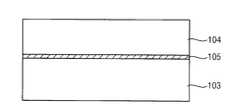
도 1a, 1b는 실시예 1에 따른 반도체 장치에서 이종 접합 반도체 장치에서 산화물 반도체와 금속 배선층 사이를 연결하는 저 저항 컨택층을 형성하는 방법을 설명하는 단면도들이다.1A and 1B are cross-sectional views illustrating a method of forming a low-resistance contact layer connecting an oxide semiconductor and a metal wiring layer in a heterojunction semiconductor device in the semiconductor device according to the first embodiment.
도 1a 및 도 1b를 참조하면, 실리콘 반도체 박막의 경우, 금속 배선층(104)과 접합을 만들 때 도핑이 많이 된 실리콘층, n+ Si을 쇼트키 장벽을 극복하는 저 저항 컨택층(106)으로 사용해왔다. 이는 식 1이 나타내듯이 접촉 저항이 도핑 농도가 높을 때 낮아지는 물리적 특성을 이용한 것이다.1A and 1B, in the case of a silicon semiconductor thin film, a doped silicon layer and n + Si are used as a low-
Rc =A exp[(2ΦBn (N/m*εs)1/2)/{h coth(qh/2kT(N/m*εs)1/2)}] ........(식1)(N / m *? S) 1/2) / {hcoth (qh / 2kT (N / m *? S) 1/2)} ... Rc = A exp [ )
여기서, Rc 는 접촉저항, N은 도핑 농도, ΦBn 은 전자 이동에 대한 에너지 장벽의 높이, T는 절대 온도를 나타낸다.Where Rc is the contact resistance, N is the doping concentration,? Bn is the height of the energy barrier for electron transfer, and T is the absolute temperature.
그러나, 실리콘 반도체가 n+ Si층을 금속 배선층(104) 사이에 저 저항 컨택층(106)으로 사용한 것처럼 산화물 반도체 장치에서는 도핑 농도를 높인 산화물 반도체층(103)을 저 저항 컨택층(106)으로 활용하기 어렵다. 이는 산화물 반도체(103)를 구성하는 조성계에서 전자 이동도를 생성하는 도판트의 고용량이 제한적 이기 때문이다.However, in the oxide semiconductor device, as the silicon semiconductor uses the n + Si layer as the low-
본 발명의 실시예에서는 전도성이 높은 비화학양론적 산화물층을 이용해 산화물 반도체층(103)과 금속 배선층(104) 사이에 형성된 에너지 장벽을 낮추는 방법을 나타내었다. 산화물 반도체층(103)은 Zn-O, In-O, Sn-O, Ga-O 또는 Hf-O 조성계로 이루어진 비정질 상태, 결정질 상태 또는 비정질 상태와 결정질 상태가 공존하는 미세 결정질 상태 중 어느 하나의 상태로 존재한다.A method of lowering the energy barrier formed between the
전도층을 보다 향상하기 위하여 이종 양이온을 산화물 반도체층(103) 내에 첨가하는 경우, 이때의 양이온은 Li, Na, K, Rb 또는 Cs을 포함하는 주기율표 1 족, B, Ga, In 또는 Ti을 포함하는 13족, C, Si, Ge, Sn 또는 Pb를 포함하는 14족, N, P, As, Sb 또는 Bi를 포함하는 15족 또는 F, Cl, Br, I를 포함하는 17족 중 적어도 어느 하나의 족 내의 원소로 이루어진다.When heteroatoms are added to the
도판트의 주입 없이도 비정질 상태, 결정질 상태 또는 비정질 상태와 결정질 상태가 공존하는 미세 결정질 상태의 ZnO, In-O, Sn-O, Ga-O 또는 Hf-O 중 어느 하나의 결정계가 사용될 수 있다. InGaO3(ZnO)5, MgxZn1-xO, CdxZn1-xO, CdO 또는 In-Ga-Zn-O 기반의 비정질 산화물 반도체(103) a-IGZO 역시 도판트 주입 없이 적용될 수 있다.In-O, Sn-O, Ga-O or Hf-O may be used in the amorphous state, the crystalline state, or the microcrystalline state in which the amorphous state and the crystalline state coexist without dopant implantation. The amorphous oxide semiconductor (103) a-IGZO based on InGaO3 (ZnO) 5, MgxZn1-xO, CdxZn1-xO, CdO or In-Ga-Zn-O can also be applied without dopant implantation.
산화물 반도체층(103)은 스퍼터링법에 의해 예를 들어 챔버내 진공 압력은 0.4Pa, 가스 혼합비는 Ar(argon):O2=50:5에서 25nm에서 500nm 두께로 형성한 다음 0.05% 농도의 플로린계 산성액으로 에칭하여 제조한다. 산화물 반도체층(103)은 스퍼터링 공정 챔버 내에서의 산화 반응을 염려하지 않아도 되므로 비정질 실리콘층 을 사용한 반도체층에 대비하여 값 비싼 고 진공 분위기가 요구되지는 않는다.The
산화물 반도체층(103) 증착 후 그 위에 저 저항 금속 배선층(104)으로 Ag, Al, Au, Cu 또는 이들의 합금 박막층(105)이 스퍼터링 법 등에 의해 형성된다. 그러나, 스퍼터링 법 등에 의한 증착 공정 초기에 적어도 하나 이상의 합금 박막층(105) 원소가 첨가된다.After the
예를 들어, Ta 또는 Nb 합금 박막층(105)이 금속 배선층(104)에 첨가될 때 적어도 Ta 또는 Nb 스퍼터링 타겟 중 하나가 Al 스퍼터링 타겟과 함께 스퍼터 챔버 내에 배치된다.For example, when a Ta or Nb alloy
그 다음, Ta 또는 Nb 스퍼터링 타겟을 노출하는 셔터를 증착 공정 초기에 짧은 시간 동안 열어 둔다. 그 짧은 시간 동안 Ta 또는 Nb 그리고 금속 배선층(104) 금속 Al이 동시에 기판에 스퍼터링 증착되어 5에서 50nm 두께의 합금 박막층(105) 박막을 형성하고, 연속하여 금속 배선층(104) 금속 Al이 50에서 500nm 두께로 증착된다.A shutter exposing the Ta or Nb sputtering target is then left open for a short period of time at the beginning of the deposition process. Ta or Nb and the metal Al of the
합금 박막층(105) 원소는 금속 배선층(104) 금속 또는 산화물 반도체(103)를 구성하는 구성 원소를 고려하여 결정되는 게 바람직하다. 예를 들어, 식 2와 같이 깁스 형성 자유 에너지로 대표되는 산소 원소에 대한 상대적 친화성이 디자인 룰이 될 수 있다.It is preferable that the alloy
ΔGMOx ≤ ΔGAOx or ΔGCOx .......(식2)? GMOx?? GAOx or? GCOx (2)
여기서, M은 합금 박막층(105) 원소, A는 금속 배선층(104) 금속, C는 산화물 반도체(103)를 구성하는 양이온 또는 불순물에 해당한다. G는 화학적 반응에 대 한 열역학적 포텐셜을 나타내는 깁스 자유 에너지를 나타낸다. 깁스 자유에너지가 낮은 값일수록 산화물을 형성하려는 경향이 강하다. 산화물 형성에 대한 깁스 자유 에너지를 'The Oxide handbook, G V Samsonov New York 1982.'를 참조하여 표 1에 나타내었다.Here, M corresponds to an alloy
예를 들어, ZnO 산화물 반도체(103) 위에 금속 배선층(104) 금속으로 Al을 적용할 경우, Al과 ZnO 사이 계면에 첨가할 합금 박막층(105) 원소로 Ta 또는 Nb가 적당하다. 표 1에서 나타내었듯이, Al2O3을 형성하는 깁스 자유 에너지가 -1492, ZnO를 형성하는 깁스 자유 에너지가 -324 이며, Ta2O5와 Nb2O5에 대한 깁스 자유 에너지가 각각 -1910.991 그리고 -1765로 식 2를 만족한다. 즉, Al2O3이 형성되는 것 보다 Ta2O5 또는 Nb2O5를 형성하려는 힘이 강하다는 의미이다. 식 2를 이용하여 물질을 선택할 경우, 깁스 자유 에너지는 온도의 함수이므로 동일 온도에서 비교되어야 함을 주의하여야 한다.For example, when Al is applied to the
(표 1)(Table 1)

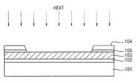
도 1B에서 나타내었듯이, 산화물 반도체(103)와 금속 배선층(104)의 접합체는 약 400oC 또는 그 이하의 온도에서 열처리된다. 열처리는 질소 분위기 또는 산소 분위기의 가열로, RTA, 가열판 또는 레이저 장치를 이용하여 이루어질 수 있다.As shown in Fig. 1B, the junction body of the
산화물 반도체층(103)의 결정성은 열처리에 의해 증가된다. 특히 깁스 자유에너지 룰에 의해 디자인 된 것처럼, 산화물 반도체층(103) 내부의 산소 원자는 금속 배선층(104) 물질 원소 또는 산화물 반도체(103)를 내부 금속 원자 보다 비화학 양론적 산화물을 유도한 합금 박막층(105) 원소 쪽으로 결합된다.The crystallinity of the
저 저항 컨택층(106), 비화학양론적 산화물 MOx는 0.5에서 50nm의 두께로 얇게 형성되어, 소위 터널링 효과를 통해 산소 공공을 통해 전자를 반대쪽층으로 이동시킨다.The low-
도 2a 및 도 2b는 도 1a 및 도 1b에서 도시된 저 저항 컨택층을 통한 터널링 효과를 설명하는 밴드 다이어그램이다.2A and 2B are band diagrams illustrating the tunneling effect through the low-resistance contact layer shown in FIGS. 1A and 1B.
여기서 Evac은 진공의 에너지 수준을, EF는 페르미 에너지 수준으로 전자 충전 확률이 50%가 되는 에너지 수준을 의미한다. Here, Evac means the energy level of the vacuum, and EF means the energy level at which the electron charging probability is 50% at the Fermi energy level.
도 2a 및 도 2b를 참조하면, Al층이 ZnO층을 전기적으로 접촉하게 되면, 도 2A에 나타낸 것과 같이 Al과 ZnO 각각의 고유한 페르미 에너지 수준 차이로 인해 접촉 경계 면에서 쇼트키 에너지 장벽이 발생한다. 반도체 에너지 밴드가 굽은 형상이 되며, 전자가 접촉 계면에 형성된 쇼트키 에너지 장벽을 통과하는 현상이 억제된다. 그러나, Ta 원소가 접촉 계면에서 열처리에 의해 비화학양론적 산화물 TaOx로 산화되면, 전자가 쉽게 에너지 장벽을 통과할 수 있도록 에너지 우물이 형성된다.Referring to FIGS. 2A and 2B, when the Al layer is in electrical contact with the ZnO layer, a Schottky barrier occurs at the contact interface due to the difference in the Fermi energy level between Al and ZnO, do. The semiconductor energy band becomes a curved shape and the phenomenon that electrons pass through the Schottky energy barrier formed on the contact interface is suppressed. However, when the Ta element is oxidized to the nonstoichiometric oxide TaOx by heat treatment at the contact interface, energy wells are formed so that electrons can easily pass through the energy barrier.
실시예 2Example 2
실시예 2는 저 저항 접촉층이 형성되고, 박막 결정성이 향상되는 질화물 반도체 장치 및 그 제조 방법에 관한 것이다. 실시 예 2는 산화물 반도체층 대신 질화물 반도체층이 형성된 것을 제외하고 실시예 1과 실질적으로 동등하다.Example 2 relates to a nitride semiconductor device in which a low-resistance contact layer is formed and thin film crystallinity is improved, and a manufacturing method thereof. Embodiment 2 is substantially equivalent to Embodiment 1 except that a nitride semiconductor layer is formed instead of an oxide semiconductor layer.
본 발명의 기술적 특징은 전도성이 높은 비화학양론적 질화물 반도체를 질화 물 반도체와 금속 배선층(104) 사이에 삽입하여 식 1에서 나타난 에너지 장벽, ΦBn을 낮추는데 있다.The technical feature of the present invention is to insert a highly conductive non-stoichiometric nitride semiconductor between the nitride semiconductor and the
질화물 반도체 박막은 Ga-N, In-N, Zn-N 또는 Al-N 조성 시스템으로 이루어진 비정질 상태, 결정질 상태 또는 비정질 상태와 결정질 상태가 공존하는 미세 결정질 상태 중 어느 하나의 상태로 존재한다. 전도층을 보다 향상하기 위하여 이종 양이온을 산화물 반도체층(103) 내에 첨가하는 경우,The nitride semiconductor thin film is in an amorphous state, a crystalline state, or a microcrystalline state in which a crystalline state coexists with GaN, In-N, Zn-N, or Al-N composition systems. When hetero-cations are added in the
이때의 양이온은 Li, Na, K, Rb 또는 Cs을 포함하는 주기율표 1 족, B, Ga, In 또는 Ti을 포함하는 13족, C, Si, Ge, Sn 또는 Pb를 포함하는 14족, N, P, As, Sb 또는 Bi를 포함하는 15족 또는 F, Cl, Br, I을 포함하는 17족 중 적어도 어느 하나의 족 내의 원소로 이루어진다. 도판트의 주입 없이도 비정질 상태, 결정질 상태 또는 비정질 상태와 결정질 상태가 공존하는 미세 결정질 상태의 Ga-N, In-N, Zn-N 또는 Al-N 중 어느 하나의 결정계가 사용될 수 있다.In this case, the cations include Group 13 elements of Group 1 of the periodic table including Li, Na, K, Rb or Cs, Group 13 elements of B, Ga, In or Ti, Group 14 elements of C, Si, Ge, Sn or Pb, P, As, Sb or Bi, or an element in at least any one group of the group consisting of F, Cl, Br, and I. In-N, In-N, Zn-N or Al-N may be used in a microcrystalline state in which an amorphous state, a crystalline state, or an amorphous state and a crystalline state coexist without implantation of a dopant.
질화물 반도체층은 스퍼터링법에 의해 예를 들어 챔버내 진공 압력은 0.4Pa, 가스 혼합비는 Ar(argon):N2=50:5에서 25nm에서 500nm 두께로 형성한 다음 0.05% 농도의 플로린계 산성액으로 에칭하여 제조한다. 질화물 반도체층은 스퍼터링 공정 챔버 내에서의 질화 반응을 염려하지 않아도 되므로 비정질 실리콘층을 사용한 반도체층에 대비하여 값 비싼 고 진공 분위기가 요구되지는 않는다.The nitride semiconductor layer is formed by a sputtering method, for example, at a vacuum pressure of 0.4 Pa in the chamber and a gas mixture ratio of 25 nm to 500 nm at a ratio of Ar (argon): N2 = 50: 5, Etched. The nitride semiconductor layer does not need to worry about the nitridation reaction in the sputtering process chamber, so a high vacuum atmosphere which is expensive in comparison with the semiconductor layer using the amorphous silicon layer is not required.
질화물 반도체층 증착 후 그 위에 저 저항 금속 배선층(104)으로 Ag, Al, Au, Cu 또는 이들의 합금 박막층(105)이 스퍼터링 법 등에 의해 형성된다. 그러나, 스퍼터링 법 등에 의한 증착 공정 초기에 적어도 하나 이상의 합금 박막층(105) 원 소가 첨가된다.After the nitride semiconductor layer is deposited, Ag, Al, Au, Cu or an alloy
예를 들어, Ta 또는 Nb 합금 박막층(105)이 금속 배선층(104)에 첨가될 때 적어도 Ta 또는 Nb 스퍼터링 타겟 중 하나가 Al 스퍼터링 타겟과 함께 스퍼터 챔버 내에 배치된다. 그 다음, Ta 또는 Nb 스퍼터링 타겟을 노출하는 셔터를 증착 공정 초기에 짧은 시간 동안 열어 둔다. 그 짧은 시간 동안 Ta 또는 Nb 그리고 금속 배선층(104) 금속 Al이 동시에 기판에 스퍼터링 증착하여 5nm에서 50nm 두께의 합금 박막층(105) 박막을 형성하고, 연속하여 금속 배선층(104) 금속 Al이 50에서 500nm 두께로 증착한다. 합금 박막층(105) 원소는 금속 배선층(104) 금속 또는 질화물 반도체를 구성하는 구성 원소를 고려하여 결정되는 게 바람직하다. 예를 들어, 식 2와 같이 깁스 형성 자유 에너지로 대표되는 질소 원소에 대한 상대적 친화성이 디자인 룰이 될 수 있다.For example, when a Ta or Nb alloy
ΔGMOx ≤ ΔGAOx or ΔGCOx .......(식2)? GMOx?? GAOx or? GCOx (2)
여기서, M은 합금 박막층(105) 원소, A는 금속 배선층(104) 금속, C는 질화물 반도체를 구성하는 양이온 또는 불순물에 해당한다. G는 화학적 반응에 대한 열역학적 포텐셜을 나타내는 깁스 자유 에너지를 나타낸다.Here, M corresponds to an alloy
깁스 자유에너지가 낮은 값일수록 질화물을 형성하려는 경향이 강하다. 질화물 형성에 대한 깁스 자유 에너지를 The Oxide handbook, G V Samsonov New York 1982.를 참조하여 표 1에 나타내었다.The lower the value of Gibbs free energy, the stronger the tendency to form nitride. Gibbs free energy for nitride formation is shown in Table 1 with reference to The Oxide handbook, G V Samsonov New York 1982. [
예를 들어, GaN 질화물 반도체 위에 금속 배선층(104)으로 Al을 적용할 경우, Al과 GaN 사이 계면에 첨가할 합금 박막층(105) 원소로 Ta 또는 Nb가 적당하 다. 표 2에서 나타내었듯이, AlN을 형성하는 깁스 자유 에너지가 -286.997, GaN를 형성하는 깁스 자유 에너지가 -77.7이며, TiN, ZrN 또는 Mg3N2에 대한 깁스 자유 에너지가 각각 -309.155, -336, -400.498로 식 2를 만족한다.For example, when Al is applied to the
즉, AlN가 형성되는 것 보다 TiN, ZrN 또는 Mg3N2를 형성하려는 힘이 강하다는 의미이다. 식 2를 이용하여 물질을 선택할 경우, 깁스 자유 에너지는 온도의 함수이므로 동일 온도에서 비교되어야 함을 주의하여야 한다.That is, it means that the force to form TiN, ZrN or Mg3N2 is stronger than that of AlN. It should be noted that when selecting materials using Equation 2, Gibbs free energy is a function of temperature and must be compared at the same temperature.
(표 2)(Table 2)

도 1B에서 나타내었듯이, 질화물 반도체와 금속 배선층(104)의 접합체는 약 400oC 또는 그 이하의 온도에서 열처리된다. 열처리는 질소 분위기 또는 산소 분위기의 가열로, RTA, 가열판 또는 레이저 장치를 이용하여 이루어질 수 있다. 질화물 반도체층의 결정성은 열처리에 의해 증가된다. 특히 깁스 자유에너지 룰에 의해 디자인 된 것처럼, 질화물 반도체층 내부의 질소 원자는 금속 배선층(104) 물질 원소 또는 질화물 반도체를 내부 금속 원자 보다 비화학양론적 질화물을 유도한 합금 박막층(105) 원소 쪽으로 결합된다.As shown in FIG. 1B, the junction body of the nitride semiconductor and the
저 저항 컨택층(106), 비화학양론적 질화물 MNx는 0.5에서 50nm의 두께로 얇게 형성되어, 소위 터널링 효과를 통해 산소 공공을 통해 전자를 반대쪽층으로 이동시킨다. 도 2A와 도 2B는 비화학양론적 질화물 MNx 삽입층에 의한 터널링 효과를 설명하는 에너지 밴드 다이어그램을 나타낸다. 여기서 Evac은 진공의 에너지 수준을, EF는 페르미 에너지 수준으로 전자 충전 확률이 50%가 되는 에너지 수준을 의미한다. Al층이 GaN층을 전기적으로 접촉하게 되면, 도 2A에 나타낸 것과 같이 Al과 GaN 각각의 고유한 페르미 에너지 수준 차이로 인해 접촉 경계 면에서 쇼트키 에너지 장벽이 발생한다. 반도체 에너지 밴드가 굽은 형상이 되며, 전자가 접촉 계면에 형성된 쇼트키 에너지 장벽을 통과하는 현상이 억제된다. 그러나, Ti 원소가 접촉 계면에서 열처리에 의해 비화학양론적 질화물 TiN으로 질화되면, 전자가 쉽게 에너지 장벽을 통과할 수 있도록 에너지 우물이 형성된다.The low-
실시예 3Example 3
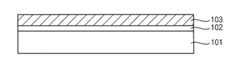
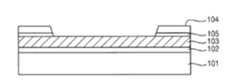
박막 트랜지스터를 포함하는 반도체 장치에 관한 실시예이다. 도 3a 내지 도 3h는 도 1a 내지 도 2b에서 설명된 반도체 장치의 제조 방법의 공정도들이다.This embodiment relates to a semiconductor device including a thin film transistor. 3A to 3H are process drawings of the method of manufacturing the semiconductor device described in Figs. 1A to 2B.
본 실시예에서 바륨 보론실리케이트 글라스, 알루미늄 보론실리케이트 글라스, 플라스틱 또는 PET, PEN, PES, 아크릴, 폴리이미드와 같은 레진 계통의 기판이 사용될 수 있다. In this embodiment, a resin-based substrate such as barium boron silicate glass, aluminum boron silicate glass, plastic or PET, PEN, PES, acrylic, polyimide may be used.
이산화 실리콘층, 질화 실리콘층 또는 이들의 적층된 구조로 이루어진 절연층이 베이스층(102)으로 사용될 수 있다. 베이스층(102)은 스퍼터링 법 또는 CVD법 등이 사용된다. 베이스층(102)은 필수적인 것은 아니며, 융점이 낮은 기판을 사용할수록 필요하게 된다.An insulating layer made of a silicon dioxide layer, a silicon nitride layer, or a laminated structure thereof may be used as the
산화물 반도체(103)는 스퍼터링법에 의해 25nm에서 500nm 두께로 베이스 필름 위에 형성된다. 예를 들어 아연 산화물(ZnO), InGaO3(ZnO)5, 마그네슘 아연 산화물(MgxZn1-xO), 카드뮴 아연 산화물(CdxZn1-xO), 카드뮴 산화물(CdO), 또는 In-Ga-Zn-O 기반의 비정질 산화물 반도체(a-IGZO)가 사용된다, 비정질 상태, 결정질 상태 또는 비정질과 결정질이 공존하는 마이크로 결정질 상태로 존재한다. 베이스 산화물로는 Zn-O계뿐만 아니라, In-O, Sn-O, Ga-O 또는 Hf-O 조성계가 사용될 수 있다.The
은(Ag), 알루미늄(Al), 금(Au), 구리(Cu) 또는 이들의 합금 박막층(105)으로 이루어진 금속 배선층(104)이 산화물 반도체층(103) 위에 형성된다. 짧은 시간 동안 스퍼터링법에 의해 동시 증착하여 매우 얇은 혼합 합금 박막층(105)을 형성하고, 진공을 유지한 상태에서 연속적으로 금속 배선층(104) 금속을 50nm에서 500nm사이의 두께로 혼합 합금 박막층(105) 위에 증착된다.A
적층 구조는 질소 충전 분위기의 가열로, RTA 또는 레이저 방법에 의해 약 400oC 온도로 가열한다. 금속 배선층(104) 또는 합금 박막층(105) 원소는 비화학양론적 비정질 산화물층을 형성하여 터널링 효과에 의한 전자 이동을 용이하게 한다.The laminated structure is heated to a temperature of about 400 캜 by RTA or laser method by heating in a nitrogen-filled atmosphere. The
게이트 절연층(107)은 두께 50nm에서 500nm 사이의 두께로 산화물 반도체(103) 위에 형성된다. 게이트 절연층(107)은 실리콘 산화물 또는 실리콘 질화물을 포함한 단일층 또는 이들의 적층 구조로 스퍼터링 법 또는 플라즈마 CVD등의 다양한 CVD법에 의해 형성된다. 게이트 절연층(107)으로는 알루미나(Al2O3), 알루미늄 질화물(AlN), 타이타늄 산화물(TiO2), 지르코니아(ZrO2), 리튬 산화물(Li2O), 칼륨 산화물(K2O), 나트륨 산화물(Na2O), 인듐 산화물(In2O3), 이트륨 산화물(Y2O3), 또는 칼슘 지르코늄 산화물(CaZrO3) 단일층 또는 이들 중 적어도 둘 이상의 복합층으로 형성될 수 있다.The
다음 제조 공정 단계에서, 게이트 전극(108)을 100nm에서 200nm 사이의 두께로 스퍼터링법에 의해 게이트 절연층(107) 위에 형성할 수 있다. 게이트 전극(108)은 (Ag), 알루미늄(Al), 금(Au), 구리(Cu) 또는 탄탈륨(Ta), 텅스텐(W), 타이타늄(Ti), 몰리브데늄(Mo), 크로륨(Cr), 니오븀(Nb) 또는 이 중 둘 이상의 합금 박막층(105) 또는 복합층으로 구성할 수 있다. 또는 인(P), 아르세닉(As)등이 도핑된 다결정 실리콘 반도체 물질로 형성될 수 있다.In the next manufacturing step, the
형성된 TFT를 보호하기 위한 보호층(109)은 플라즈마 CVD, 스퍼터링법에 의해 실리콘 질화물, 실리콘 산화물, 실리콘 질소산화물, 실리콘 산소질화물, 알루미늄 산소질화물, 알루미늄 산화물, 다이아몬드상 탄소(DLC), 질화탄소 등의 절연층에 의해 형성된다. 보호층(109)은 단일층뿐 아니라 둘 이상의 복합층으로 형성되는 것도 가능하다.The
실시예 4Example 4
도 4a 내지 도 4f는 일 실시예에 따른 예시적인 박막 장치를 내포한 디스플레이 장치의 구조를 나타낸 단면도이다.4A to 4F are cross-sectional views illustrating a structure of a display device including an exemplary thin film device according to an embodiment.
도 4a 내지 도 4f를 참조하면, 실시예 4는 액정 표시 장치를 제조하는 방법을 나타낸다. 좀 더 자세하게는 스토리지 전극과 픽셀 전극이 연결된 역 스태거 타입의 TFT를 나타낸다. 회로 기판의 금속 배선층(104)에 전기적으로 연결하기 위한 기판 끝단 부에 위치한 터미널 (201)을 동시에 제조하는 방법이 도시되었다.4A to 4F, Embodiment 4 shows a method of manufacturing a liquid crystal display device. More specifically, it shows a reverse stagger type TFT in which a storage electrode and a pixel electrode are connected. A method of simultaneously manufacturing a terminal 201 located at a substrate end for electrically connecting to a
바륨 보론실리케이트 글라스, 알루미늄 보론실리케이트 글라스, 플라스틱 또는 PET, PEN, PES, 아크릴, 폴리이미드와 같은 레진 계통의 기판이 사용될 수 있다.Barium boron silicate glass, aluminum boron silicate glass, plastic or resin based substrates such as PET, PEN, PES, acrylic, and polyimide may be used.
기판 위 전면에 도전층을 형성한 다음 제1 리소그래피가 실시된다. 레지스터 마스크를 형성하고 불필요한 영역을 에칭함에 의해 금속 배선층(104)과 전극(게이트 전극, 유지전극, 터미널 전극)이 형성된다.A first lithography is performed after forming a conductive layer over the entire surface of the substrate. The
게이트 전극(108)을 100nm에서 200nm 사이의 두께로 스퍼터링법에 의해 게이트 절연층(107) 위에 형성할 수 있다. 게이트 전극(108)은 은 (Ag), 알루미늄(Al), 금(Au), 구리(Cu) 또는 탄탈륨(Ta), 텅스텐(W), 타이타늄(Ti), 몰리브데늄(Mo), 크로륨(Cr), 니오븀(Nb) 또는 이 중 둘 이상의 합금 박막층(105) 또는 복합층으로 구성할 수 있다. 또는 인(P), 아르세닉(As)등이 도핑된 다결정 실리콘 반도체 물질로 형성될 수 있다.The
게이트 절연층(107)은 두께 50nm에서 500nm 사이의 두께로 산화물 반도체(103) 위에 형성된다. 게이트 절연층(107)은 실리콘 산화물 또는 실리콘 질화물 을 포함한 단일층 또는 이들의 적층 구조로 스퍼터링 법 또는 플라즈마 CVD등의 다양한 CVD법에 의해 형성된다. 게이트 절연층(107)으로는 알루미나(Al2O3), 알루미늄 질화물(AlN), 타이타늄 산화물(TiO2), 지르코니아(ZrO2), 리튬 산화물(Li2O), 칼륨 산화물(K2O), 나트륨 산화물(Na2O), 인듐 산화물(In2O3), 이트륨 산화물(Y2O3), 또는 칼슘 지르코늄 산화물(CaZrO3) 단일층 또는 이들 중 적어도 둘 이상의 복합층으로 형성될 수 있다.The
다음 제조 방법으로 산화물 반도체(103)는 스퍼터링법에 의해 25nm에서 500nm 두께로 베이스 필름 위에 형성할 수 있다. 예를 들어 아연 산화물(ZnO), InGaO3(ZnO)5, 마그네슘 아연 산화물(MgxZn1-xO), 카드뮴 아연 산화물(CdxZn1-xO), 카드뮴 산화물(CdO), 또는 In-Ga-Zn-O 기반의 비정질 산화물 반도체(a-IGZO)가 사용된다, 비정질 상태, 결정질 상태 또는 비정질과 결정질이 공존하는 마이크로 결정질 상태로 존재한다. 베이스 산화물로는 Zn-O계 뿐만 아니라, In-O, Sn-O, Ga-O 또는 Hf-O 조성계가 사용될 수 있다.The
은(Ag), 알루미늄(Al), 금(Au), 구리(Cu) 또는 이들의 합금 박막층(105)으로 이루어진 금속 배선층(104)이 산화물 반도체층 위에 형성된다. 짧은 시간 동안 스퍼터링법에 의해 동시 증착하여 매우 얇은 혼합 합금 박막층(105)을 형성하고, 진공을 유지한 상태에서 연속적으로 금속 배선층(104) 금속을 50nm에서 500nm사이의 두께로 혼합 합금 박막층(105) 위에 증착된다.A
제2 리소그래피 공정을 실시한다. 레지스터 마스크를 형성하고 불필요한 영역을 식각하여 금속 배선층(104)과 전극(소스전극)이 형성된다. 습식 식각 또는 건 식 식각이 일반적으로 사용된다. 실시예 3에서는 산화물 반도체층(103), 저 저항 컨택층(106), 도전층을 식각하여 TFT 영역에 형성하고, Al 또는 Cu층을 SiCl4, Cl2, and BCl3 반응 가스 또는 이 중 둘 이상의 혼합 가스에 의해 식각된다. 레지스터 마스크를 제거한 후, 인듐 산화물(In2O3) 또는 ITO (In2O3SnO2) 와 같은 투명한 전도층을 스퍼터링 법 또는 진공 증발 증착등에 의해 전면 형성된다.A second lithography process is performed. A resist mask is formed and an unnecessary region is etched to form a
세 번째 리소그래피 공정을 실시한다. 레지스터 마스크에 의해 의 일부를 동시에 식각하여 반도체 영역(103), 소스 전극(208), 드레인 전극(209), 픽셀 전극(210)이 형성된다.A third lithography process is performed. A
실시예 4에서는 ITO로 이루어진 픽셀 전극이 첫번째로 질산, 염산 또는 이들의 혼합 용액에 의해 선택적으로 습식 식각 되고, 전도층, 저 저항 컨택층(106) 그리고 산화물 반도체층(103)의 일부분이 건식 식각되어 오픈 부가 형성된다. 그러나, 적절한 반응 가스를 선택함에 의해 건식 식각으로만 공정을 진행할 수도 있고, 적절한 반응액을 선택함에 의해 습식 식각으로만 공정을 진행할 수도 있다.In Embodiment 4, the pixel electrode made of ITO is first wet-etched selectively by nitric acid, hydrochloric acid or a mixed solution thereof, and the conductive layer, the low-
오픈 부는 비정질 반도체층의 중간 영역까지 식각되어 비정질 반도체층의 오목한 영역을 형성한다. 전도층은 오픈 부에 의해 소스 전극(208)과 드레인 전극(209)이 분리되어 형성되고, 저 저항 컨택층(106)도 소스 부, 드레인 부 영역이 구별되게 된다. 소스 전극과 접촉하고 있는 투명 전도층은 소스 전극(208)을 덮고, 이어지는 타 제조 공정에서, 특히 러빙 공정에서 정전기를 방지하는 역할을 한다.The open portion is etched to an intermediate region of the amorphous semiconductor layer to form a concave region of the amorphous semiconductor layer. The
투명 전도층은 상기 언급된 ITO층을 식각하는 동안 제거된다. 한편, 스토리지 배선(203)이 세 번째 리소그래피 공정에 의해 형성된다. 스토리지배선(203)과 픽셀 전극(210) 사이에 스토리지배선(203) 위에 형성된 절연층을 유전체로 하여 축전 용량이 형성된다. 터미널(201)부의 투명전극도 세 번째 리소그래피 공정에 의해 형성된다. 레지스터 마스크를 제거한 다음, 다시 터미널 (201) 영역에 부분적인 레지스터 마스크를 형성하여 터미널 (201) 부를 덮고 있는 절연층을 선택적으로 제거한다 (도 4e).The transparent conductive layer is removed during the etching of the above-mentioned ITO layer. On the other hand, the
도 5는 본 발명의 예시적인 박막 장치를 내포한 디스플레이 장치의 픽셀 구조를 나타낸 평면도이다.5 is a plan view showing a pixel structure of a display device including an exemplary thin film device of the present invention.
레지스터 마스크는 쉐도우 마스크를 이용하거나 스크린 프린팅법에 의해 형성한다. 도 4E는 도 5에 도시된 AA' 와 BB' 라인을 따라 절단된 단면을 나타낸다. 이상 세 번의 리소그래피를 통해 역 스태거 타입의 n 채널형 TFT와 스토리지 전극이 완성된다. 각 픽셀에 해당하는 매트릭스 위치에 TFT를 배치함으로써, 액티브 매트릭스 액정 표시 장치를 제조할 수 있게 된다. 이후 공정에서 폴리이미드 레진 성분을 포함한 배향층(220)이 액티브 매트릭스 기판 위에 형성된다.The register mask is formed by using a shadow mask or by screen printing. Figure 4E shows a section cut along AA 'and BB' lines shown in Figure 5. Through the above three lithography processes, a reverse stagger type n-channel TFT and a storage electrode are completed. By disposing the TFTs at the matrix positions corresponding to the respective pixels, an active matrix liquid crystal display device can be manufactured. In the subsequent process, an
액티브 매트릭스 기판과 대향 전극(231)과 대향 배향층(232)이 형성된 대향 기판(230) 사이에 액정(240)을 주입하고 스페이서에 의해 일정한 샐갭을 유지하며 실런트 접합한다. TN 액정 또는 VA 액정이 주입된다. 플렉서블 인쇄 회로(FPC)는 터미널 (201)에 연결된다. 플렉서블 인쇄 회로(FPC)는 폴리이미드 등의 레진 기판 위에 인쇄된 배선으로 형성되고, 이방성 전도 필름(229)을 통해 터미널(201)에 연결된다. 이방성 전도 필름(229)은 수백 um 크기의 전도성 표면을 지닌 입자(227)들을 포함하여 접착제(225), 에 의해 고정된다. 입자(227)들은 터미널(201) 이방성 전도 필름 위에 형성된 구리 배선(228)을 전기적으로 연결된다. 기계적 강도를 향상하기 위해 레진(226)이 전도성 입자(227)와 함께 형성되기도 한다.The
상기에 기술된 액정 디스플레이 장치에 관한 실시예 4는 반도체 장치 실시예 1 또는 2와 결합될 수 있다.Embodiment 4 of the liquid crystal display device described above can be combined with Embodiment 1 or 2 of the semiconductor device.
본 발명에 따른 어레이 기판 및 이를 갖는 표시장치에 의하면 단위 화소의 개구율 및 시야각이 향상된다. 따라서 본 발명은 표시장치의 표시품질을 향상시키는 기술에 적용될 수 있다.According to the array substrate and the display device having the same, the aperture ratio and the viewing angle of the unit pixel are improved. Therefore, the present invention can be applied to a technique for improving the display quality of a display device.
앞서 설명한 본 발명의 상세한 설명에서는 본 발명의 바람직한 실시예들을 참조하여 설명하였지만, 해당 기술분야의 숙련된 당업자 또는 해당 기술분야에 통상의 지식을 갖는 자라면 후술될 특허청구범위에 기재된 본 발명의 사상 및 기술 영역으로부터 벗어나지 않는 범위 내에서 본 발명을 다양하게 수정 및 변경시킬 수 있음을 이해할 수 있을 것이다.While the present invention has been described in connection with what is presently considered to be practical and exemplary embodiments, it is to be understood that the invention is not limited to the disclosed embodiments, but, on the contrary, It will be understood by those skilled in the art that various changes in form and details may be made therein without departing from the spirit and scope of the invention as defined by the appended claims.
도 1a, 1b는 일 실시예에 따른 반도체 장치에서 이종 접합 반도체 장치에서 산화물 반도체와 금속 배선층 사이를 연결하는 저 저항 컨택층을 형성하는 방법을 설명하는 단면도들이다.1A and 1B are cross-sectional views illustrating a method of forming a low-resistance contact layer connecting an oxide semiconductor and a metal wiring layer in a heterojunction semiconductor device in a semiconductor device according to an embodiment.
도 2a 및 도 2b는 도 1a 및 도 1b에서 도시된 저 저항 컨택층을 통한 터널링 효과를 설명하는 밴드 다이어그램이다.2A and 2B are band diagrams illustrating the tunneling effect through the low-resistance contact layer shown in FIGS. 1A and 1B.
도 3a 내지 도 3h는 도 1a 내지 도 2에서 설명된 반도체 장치의 제조 방법의 공정도들이다.3A to 3H are process drawings of the method of manufacturing the semiconductor device described in Figs. 1A to 2.
도 4a 내지 도 4f는 일 실시예에 따른 예시적인 박막 장치를 내포한 디스플레이 장치의 구조를 나타낸 단면도이다.4A to 4F are cross-sectional views illustrating a structure of a display device including an exemplary thin film device according to an embodiment.
도 5는 본 발명의 예시적인 박막 장치를 내포한 디스플레이 장치의 픽셀 구조를 나타낸 평면도이다. 5 is a plan view showing a pixel structure of a display device including an exemplary thin film device of the present invention.
<도면의 주요부분에 대한 부호의 설명> Description of the Related Art
101 : 기판102 : 베이스층101: substrate 102: base layer
103 : 산화물 반도체104 : 금속 배선층103: oxide semiconductor 104: metal wiring layer
105 : 합금 박막층105: alloy thin film layer
106 : 저 저항 컨택층107 : 게이트 절연층106: Low-resistance contact layer 107: Gate insulating layer
108 : 게이트 전극 109 : 보호층108: gate electrode 109: protective layer
201 : 터미널 202 : 게이트 배선201: Terminal 202: Gate wiring
203 : 스토리지 배선 204 : 데이터 배선203: storage wiring 204: data wiring
205 : 투명 전도층 208 : 제 1 레지스터 마스크205: transparent conductive layer 208: first resistor mask
213 : 제 3 레지스터 마스크206 : 소스 영역213: third register mask 206: source region
207 : 드레인 영역 208 : 소스 전극207: drain region 208: source electrode
209 : 드레인 전극210 : 픽셀 전극209: drain electrode 210: pixel electrode
220 : 제 1 배향층230 : 대향 기판220: first orientation layer 230: opposing substrate
225 : 접착제 226 : 레진225: Adhesive 226: Resin
227 : 도전 입자 228 : 구리 배선227: conductive particles 228: copper wiring
229 : 이방성 전도 필름231 : 대향 전극229: anisotropic conductive film 231: opposing electrode
232 : 제 2 배향층240 : 액정232: second orientation layer 240: liquid crystal
Claims (23)
Translated fromKoreanPriority Applications (4)
| Application Number | Priority Date | Filing Date | Title |
|---|---|---|---|
| KR1020080044144AKR101461127B1 (en) | 2008-05-13 | 2008-05-13 | Semiconductor device and method for manufacturing the same |
| US12/333,831US8067276B2 (en) | 2008-05-13 | 2008-12-12 | Semiconductor device and manufacturing method thereof |
| US13/183,711US8383465B2 (en) | 2008-05-13 | 2011-07-15 | Semiconductor device and manufacturing method thereof |
| US13/775,777US8703549B2 (en) | 2008-05-13 | 2013-02-25 | Semiconductor device and manufacturing method thereof |
Applications Claiming Priority (1)
| Application Number | Priority Date | Filing Date | Title |
|---|---|---|---|
| KR1020080044144AKR101461127B1 (en) | 2008-05-13 | 2008-05-13 | Semiconductor device and method for manufacturing the same |
Publications (2)
| Publication Number | Publication Date |
|---|---|
| KR20090118395A KR20090118395A (en) | 2009-11-18 |
| KR101461127B1true KR101461127B1 (en) | 2014-11-14 |
Family
ID=41602359
Family Applications (1)
| Application Number | Title | Priority Date | Filing Date |
|---|---|---|---|
| KR1020080044144AActiveKR101461127B1 (en) | 2008-05-13 | 2008-05-13 | Semiconductor device and method for manufacturing the same |
Country Status (2)
| Country | Link |
|---|---|
| US (3) | US8067276B2 (en) |
| KR (1) | KR101461127B1 (en) |
Families Citing this family (64)
| Publication number | Priority date | Publication date | Assignee | Title |
|---|---|---|---|---|
| US20130082232A1 (en) | 2011-09-30 | 2013-04-04 | Unity Semiconductor Corporation | Multi Layered Conductive Metal Oxide Structures And Methods For Facilitating Enhanced Performance Characteristics Of Two Terminal Memory Cells |
| US8565003B2 (en) | 2011-06-28 | 2013-10-22 | Unity Semiconductor Corporation | Multilayer cross-point memory array having reduced disturb susceptibility |
| KR101461127B1 (en)* | 2008-05-13 | 2014-11-14 | 삼성디스플레이 주식회사 | Semiconductor device and method for manufacturing the same |
| US9082857B2 (en) | 2008-09-01 | 2015-07-14 | Semiconductor Energy Laboratory Co., Ltd. | Semiconductor device comprising an oxide semiconductor layer |
| CN101719493B (en) | 2008-10-08 | 2014-05-14 | 株式会社半导体能源研究所 | Display device |
| JP5361651B2 (en) | 2008-10-22 | 2013-12-04 | 株式会社半導体エネルギー研究所 | Method for manufacturing semiconductor device |
| US8741702B2 (en)* | 2008-10-24 | 2014-06-03 | Semiconductor Energy Laboratory Co., Ltd. | Method for manufacturing semiconductor device |
| EP2180518B1 (en) | 2008-10-24 | 2018-04-25 | Semiconductor Energy Laboratory Co, Ltd. | Method for manufacturing semiconductor device |
| JP5616012B2 (en)* | 2008-10-24 | 2014-10-29 | 株式会社半導体エネルギー研究所 | Method for manufacturing semiconductor device |
| KR101667909B1 (en) | 2008-10-24 | 2016-10-28 | 가부시키가이샤 한도오따이 에네루기 켄큐쇼 | Method for manufacturing semiconductor device |
| TWI487104B (en) | 2008-11-07 | 2015-06-01 | Semiconductor Energy Lab | Semiconductor device and method of manufacturing same |
| US8390100B2 (en)* | 2008-12-19 | 2013-03-05 | Unity Semiconductor Corporation | Conductive oxide electrodes |
| EP2256795B1 (en)* | 2009-05-29 | 2014-11-19 | Semiconductor Energy Laboratory Co., Ltd. | Manufacturing method for oxide semiconductor device |
| KR101857405B1 (en) | 2009-07-10 | 2018-05-11 | 가부시키가이샤 한도오따이 에네루기 켄큐쇼 | Semiconductor device and method for manufacturing the same |
| WO2011010541A1 (en) | 2009-07-18 | 2011-01-27 | Semiconductor Energy Laboratory Co., Ltd. | Semiconductor device and method for manufacturing the same |
| KR20190045396A (en)* | 2009-09-16 | 2019-05-02 | 가부시키가이샤 한도오따이 에네루기 켄큐쇼 | Transistor |
| KR20230165355A (en) | 2009-09-16 | 2023-12-05 | 가부시키가이샤 한도오따이 에네루기 켄큐쇼 | Display device |
| KR20220127372A (en) | 2009-09-24 | 2022-09-19 | 가부시키가이샤 한도오따이 에네루기 켄큐쇼 | Oxide semiconductor film and semiconductor device |
| EP2486594B1 (en) | 2009-10-08 | 2017-10-25 | Semiconductor Energy Laboratory Co., Ltd. | Oxide semiconductor device |
| KR102246127B1 (en) | 2009-10-08 | 2021-04-29 | 가부시키가이샤 한도오따이 에네루기 켄큐쇼 | Semiconductor device |
| KR101396096B1 (en) | 2009-10-09 | 2014-05-15 | 가부시키가이샤 한도오따이 에네루기 켄큐쇼 | Semiconductor device and manufacturing method thereof |
| KR101779349B1 (en)* | 2009-10-14 | 2017-09-18 | 가부시키가이샤 한도오따이 에네루기 켄큐쇼 | Semiconductor device and manufacturing method thereof |
| CN102687400B (en) | 2009-10-30 | 2016-08-24 | 株式会社半导体能源研究所 | Logic circuit and semiconductor device |
| KR102148664B1 (en) | 2009-11-06 | 2020-08-28 | 가부시키가이샤 한도오따이 에네루기 켄큐쇼 | Semiconductor device and manufacturing method thereof |
| KR101849321B1 (en) | 2009-11-06 | 2018-04-16 | 가부시키가이샤 한도오따이 에네루기 켄큐쇼 | Semiconductor device and manufacturing method thereof |
| KR102393447B1 (en) | 2009-11-13 | 2022-05-03 | 가부시키가이샤 한도오따이 에네루기 켄큐쇼 | Semiconductor device and manufacturing method thereof |
| KR102241766B1 (en) | 2009-12-04 | 2021-04-19 | 가부시키가이샤 한도오따이 에네루기 켄큐쇼 | Semiconductor device and manufacturing method thereof |
| KR101523358B1 (en) | 2009-12-04 | 2015-05-27 | 가부시키가이샤 한도오따이 에네루기 켄큐쇼 | Display device |
| US10000411B2 (en) | 2010-01-16 | 2018-06-19 | Cardinal Cg Company | Insulating glass unit transparent conductivity and low emissivity coating technology |
| US10000965B2 (en) | 2010-01-16 | 2018-06-19 | Cardinal Cg Company | Insulating glass unit transparent conductive coating technology |
| US10060180B2 (en) | 2010-01-16 | 2018-08-28 | Cardinal Cg Company | Flash-treated indium tin oxide coatings, production methods, and insulating glass unit transparent conductive coating technology |
| CN103779426B (en)* | 2010-01-22 | 2017-01-04 | 株式会社半导体能源研究所 | Semiconductor device |
| US8552425B2 (en) | 2010-06-18 | 2013-10-08 | Semiconductor Energy Laboratory Co., Ltd. | Semiconductor device |
| TWI555205B (en)* | 2010-11-05 | 2016-10-21 | 半導體能源研究所股份有限公司 | Semiconductor device and method of manufacturing semiconductor device |
| CN103500712B (en) | 2010-12-03 | 2016-05-25 | 株式会社半导体能源研究所 | Semiconductor device |
| JP2012151453A (en)* | 2010-12-28 | 2012-08-09 | Semiconductor Energy Lab Co Ltd | Semiconductor device and driving method of the same |
| JP5975635B2 (en) | 2010-12-28 | 2016-08-23 | 株式会社半導体エネルギー研究所 | Semiconductor device |
| US9911858B2 (en) | 2010-12-28 | 2018-03-06 | Semiconductor Energy Laboratory Co., Ltd. | Semiconductor device and method for manufacturing the same |
| US9093539B2 (en) | 2011-05-13 | 2015-07-28 | Semiconductor Energy Laboratory Co., Ltd. | Semiconductor device and method for manufacturing the same |
| KR102504604B1 (en) | 2011-09-29 | 2023-02-27 | 가부시키가이샤 한도오따이 에네루기 켄큐쇼 | Semiconductor device |
| KR20130040706A (en) | 2011-10-14 | 2013-04-24 | 가부시키가이샤 한도오따이 에네루기 켄큐쇼 | Semiconductor device and method of manufacturing semiconductor device |
| WO2013054933A1 (en) | 2011-10-14 | 2013-04-18 | Semiconductor Energy Laboratory Co., Ltd. | Semiconductor device |
| JP6220526B2 (en) | 2012-02-29 | 2017-10-25 | 株式会社半導体エネルギー研究所 | Method for manufacturing semiconductor device |
| CN108054175A (en) | 2012-08-03 | 2018-05-18 | 株式会社半导体能源研究所 | Semiconductor device |
| DE102013216824B4 (en) | 2012-08-28 | 2024-10-17 | Semiconductor Energy Laboratory Co., Ltd. | semiconductor device |
| TWI611511B (en) | 2012-08-31 | 2018-01-11 | 半導體能源研究所股份有限公司 | Semiconductor device |
| CN104620390A (en) | 2012-09-13 | 2015-05-13 | 株式会社半导体能源研究所 | Semiconductor device |
| JP6351947B2 (en) | 2012-10-12 | 2018-07-04 | 株式会社半導体エネルギー研究所 | Method for manufacturing liquid crystal display device |
| TWI681233B (en) | 2012-10-12 | 2020-01-01 | 日商半導體能源研究所股份有限公司 | Liquid crystal display device, touch panel and method for manufacturing liquid crystal display device |
| WO2014073585A1 (en) | 2012-11-08 | 2014-05-15 | Semiconductor Energy Laboratory Co., Ltd. | Metal oxide film and method for forming metal oxide film |
| EP2738815B1 (en)* | 2012-11-30 | 2016-02-10 | Samsung Electronics Co., Ltd | Semiconductor materials, transistors including the same, and electronic devices including transistors |
| KR102144992B1 (en)* | 2012-11-30 | 2020-08-18 | 삼성전자주식회사 | Semiconductor material, transistor including semiconductor material and electronic device including transistor |
| US9905585B2 (en) | 2012-12-25 | 2018-02-27 | Semiconductor Energy Laboratory Co., Ltd. | Semiconductor device comprising capacitor |
| KR102680781B1 (en) | 2012-12-25 | 2024-07-04 | 가부시키가이샤 한도오따이 에네루기 켄큐쇼 | Semiconductor device |
| US9012261B2 (en)* | 2013-03-13 | 2015-04-21 | Intermolecular, Inc. | High productivity combinatorial screening for stable metal oxide TFTs |
| US9153650B2 (en) | 2013-03-19 | 2015-10-06 | Semiconductor Energy Laboratory Co., Ltd. | Oxide semiconductor |
| US9231002B2 (en) | 2013-05-03 | 2016-01-05 | Semiconductor Energy Laboratory Co., Ltd. | Display device and electronic device |
| TWI809474B (en) | 2013-05-16 | 2023-07-21 | 日商半導體能源研究所股份有限公司 | Semiconductor device |
| TWI652822B (en) | 2013-06-19 | 2019-03-01 | 日商半導體能源研究所股份有限公司 | Oxide semiconductor film and formation method thereof |
| TWI608523B (en) | 2013-07-19 | 2017-12-11 | 半導體能源研究所股份有限公司 | Oxide semiconductor film, method of manufacturing oxide semiconductor film, and semiconductor device |
| WO2015132697A1 (en) | 2014-03-07 | 2015-09-11 | Semiconductor Energy Laboratory Co., Ltd. | Semiconductor device |
| US9613803B2 (en)* | 2015-04-30 | 2017-04-04 | International Business Machines Corporation | Low defect relaxed SiGe/strained Si structures on implant anneal buffer/strain relaxed buffer layers with epitaxial rare earth oxide interlayers and methods to fabricate same |
| US11028012B2 (en) | 2018-10-31 | 2021-06-08 | Cardinal Cg Company | Low solar heat gain coatings, laminated glass assemblies, and methods of producing same |
| EP4371160A1 (en)* | 2021-07-13 | 2024-05-22 | Zinite Corporation | Thin film semiconductor switching device |
Citations (4)
| Publication number | Priority date | Publication date | Assignee | Title |
|---|---|---|---|---|
| JPH06235939A (en)* | 1993-02-12 | 1994-08-23 | Hitachi Ltd | Liquid crystal display device and manufacturing method thereof |
| KR100269328B1 (en) | 1997-12-31 | 2000-10-16 | 윤종용 | Method for forming conductive layer using atomic layer deposition process |
| KR20040066286A (en)* | 2003-01-17 | 2004-07-27 | 삼성전자주식회사 | Wire for semiconductor device, thin film transistor array panel including the wire and method for manufacturing the same |
| KR20070103231A (en)* | 2006-04-18 | 2007-10-23 | 삼성전자주식회사 | A method of manufacturing a nano semiconductor thin film, a thin film transistor using the same, and a manufacturing method thereof |
Family Cites Families (4)
| Publication number | Priority date | Publication date | Assignee | Title |
|---|---|---|---|---|
| JP5064747B2 (en) | 2005-09-29 | 2012-10-31 | 株式会社半導体エネルギー研究所 | Semiconductor device, electrophoretic display device, display module, electronic device, and method for manufacturing semiconductor device |
| EP1770788A3 (en)* | 2005-09-29 | 2011-09-21 | Semiconductor Energy Laboratory Co., Ltd. | Semiconductor device having oxide semiconductor layer and manufacturing method thereof |
| JP2007258675A (en) | 2006-02-21 | 2007-10-04 | Idemitsu Kosan Co Ltd | TFT substrate, reflective TFT substrate, and manufacturing method thereof |
| KR101461127B1 (en)* | 2008-05-13 | 2014-11-14 | 삼성디스플레이 주식회사 | Semiconductor device and method for manufacturing the same |
- 2008
- 2008-05-13KRKR1020080044144Apatent/KR101461127B1/enactiveActive
- 2008-12-12USUS12/333,831patent/US8067276B2/enactiveActive
- 2011
- 2011-07-15USUS13/183,711patent/US8383465B2/enactiveActive
- 2013
- 2013-02-25USUS13/775,777patent/US8703549B2/enactiveActive
Patent Citations (4)
| Publication number | Priority date | Publication date | Assignee | Title |
|---|---|---|---|---|
| JPH06235939A (en)* | 1993-02-12 | 1994-08-23 | Hitachi Ltd | Liquid crystal display device and manufacturing method thereof |
| KR100269328B1 (en) | 1997-12-31 | 2000-10-16 | 윤종용 | Method for forming conductive layer using atomic layer deposition process |
| KR20040066286A (en)* | 2003-01-17 | 2004-07-27 | 삼성전자주식회사 | Wire for semiconductor device, thin film transistor array panel including the wire and method for manufacturing the same |
| KR20070103231A (en)* | 2006-04-18 | 2007-10-23 | 삼성전자주식회사 | A method of manufacturing a nano semiconductor thin film, a thin film transistor using the same, and a manufacturing method thereof |
Also Published As
| Publication number | Publication date |
|---|---|
| KR20090118395A (en) | 2009-11-18 |
| US8703549B2 (en) | 2014-04-22 |
| US20130168669A1 (en) | 2013-07-04 |
| US8067276B2 (en) | 2011-11-29 |
| US20110266538A1 (en) | 2011-11-03 |
| US20100123136A1 (en) | 2010-05-20 |
| US8383465B2 (en) | 2013-02-26 |
Similar Documents
| Publication | Publication Date | Title |
|---|---|---|
| KR101461127B1 (en) | Semiconductor device and method for manufacturing the same | |
| US10290742B2 (en) | Semiconductor device including oxide semiconductor layer | |
| US10446711B2 (en) | Thin film transistor array substrate and method for manufacturing the same | |
| US8669551B2 (en) | Transistor including insertion layer and channel layer with different work functions and method of manufacturing the same | |
| TWI455320B (en) | Thin film transistor and manufacturing method thereof, and display device | |
| CN103872138B (en) | Transistor, the method for manufacturing transistor and the electronic device including the transistor | |
| KR20190110977A (en) | Semiconductor device | |
| US8207530B2 (en) | Oxide semiconductor and thin film transistor including the same | |
| US20170316953A1 (en) | Method for fabricating metallic oxide thin film transistor | |
| CN102244103A (en) | TFT substrate | |
| US10461100B2 (en) | Display device having a different type of oxide semiconductor transistor | |
| JP2007109918A (en) | Transistor and manufacturing method thereof | |
| JP2011249674A (en) | Thin-film transistor and method of manufacturing the same | |
| CN102024842A (en) | Display and method for manufacturing the same | |
| KR101132989B1 (en) | Method for producing thin film transistor and method for producing electronic optical device | |
| JP6129594B2 (en) | Method for manufacturing semiconductor device | |
| US12230626B2 (en) | Transistor | |
| JP5523896B2 (en) | Thin film transistor and manufacturing method thereof | |
| KR102227413B1 (en) | Logic device and manufacturing method thereof | |
| JP5523897B2 (en) | Thin film transistor and manufacturing method thereof | |
| JP2010045159A (en) | Thin film field effect transistor and process of fabricating the same | |
| KR102229424B1 (en) | Semiconductor device with negative differential transconductance and manufacturing method thereof | |
| CN107026208A (en) | The manufacture method of semiconductor device and semiconductor device | |
| KR101023338B1 (en) | Thin film transistor and method of manufacturing the same | |
| CN118231474A (en) | Thin film transistor, method of manufacturing the same, and display device including the same |
Legal Events
| Date | Code | Title | Description |
|---|---|---|---|
| PA0109 | Patent application | Patent event code:PA01091R01D Comment text:Patent Application Patent event date:20080513 | |
| PG1501 | Laying open of application | ||
| N231 | Notification of change of applicant | ||
| PN2301 | Change of applicant | Patent event date:20120913 Comment text:Notification of Change of Applicant Patent event code:PN23011R01D | |
| A201 | Request for examination | ||
| PA0201 | Request for examination | Patent event code:PA02012R01D Patent event date:20130508 Comment text:Request for Examination of Application Patent event code:PA02011R01I Patent event date:20080513 Comment text:Patent Application | |
| E902 | Notification of reason for refusal | ||
| PE0902 | Notice of grounds for rejection | Comment text:Notification of reason for refusal Patent event date:20140228 Patent event code:PE09021S01D | |
| E701 | Decision to grant or registration of patent right | ||
| PE0701 | Decision of registration | Patent event code:PE07011S01D Comment text:Decision to Grant Registration Patent event date:20140917 | |
| GRNT | Written decision to grant | ||
| PR0701 | Registration of establishment | Comment text:Registration of Establishment Patent event date:20141106 Patent event code:PR07011E01D | |
| PR1002 | Payment of registration fee | Payment date:20141107 End annual number:3 Start annual number:1 | |
| PG1601 | Publication of registration | ||
| FPAY | Annual fee payment | Payment date:20171101 Year of fee payment:4 | |
| PR1001 | Payment of annual fee | Payment date:20171101 Start annual number:4 End annual number:4 | |
| FPAY | Annual fee payment | Payment date:20191028 Year of fee payment:6 | |
| PR1001 | Payment of annual fee | Payment date:20191028 Start annual number:6 End annual number:6 | |
| PR1001 | Payment of annual fee | Payment date:20201102 Start annual number:7 End annual number:7 | |
| PR1001 | Payment of annual fee | Payment date:20211027 Start annual number:8 End annual number:8 | |
| PR1001 | Payment of annual fee | Payment date:20221025 Start annual number:9 End annual number:9 | |
| PR1001 | Payment of annual fee | Payment date:20231023 Start annual number:10 End annual number:10 | |
| PR1001 | Payment of annual fee | Payment date:20241022 Start annual number:11 End annual number:11 |