KR101454878B1 - Subatrate Embedded Horn Antenna having Selection Capability of Vertical and Horizontal Radiation Pattern - Google Patents
Subatrate Embedded Horn Antenna having Selection Capability of Vertical and Horizontal Radiation PatternDownload PDFInfo
- Publication number
- KR101454878B1 KR101454878B1KR1020130109677AKR20130109677AKR101454878B1KR 101454878 B1KR101454878 B1KR 101454878B1KR 1020130109677 AKR1020130109677 AKR 1020130109677AKR 20130109677 AKR20130109677 AKR 20130109677AKR 101454878 B1KR101454878 B1KR 101454878B1
- Authority
- KR
- South Korea
- Prior art keywords
- embedded
- antenna
- horn antenna
- substrate
- horn
- Prior art date
- Legal status (The legal status is an assumption and is not a legal conclusion. Google has not performed a legal analysis and makes no representation as to the accuracy of the status listed.)
- Expired - Fee Related
Links
Images


Classifications
- H—ELECTRICITY
- H01—ELECTRIC ELEMENTS
- H01Q—ANTENNAS, i.e. RADIO AERIALS
- H01Q13/00—Waveguide horns or mouths; Slot antennas; Leaky-waveguide antennas; Equivalent structures causing radiation along the transmission path of a guided wave
- H01Q13/02—Waveguide horns
- H01Q13/0283—Apparatus or processes specially provided for manufacturing horns
- H—ELECTRICITY
- H01—ELECTRIC ELEMENTS
- H01Q—ANTENNAS, i.e. RADIO AERIALS
- H01Q21/00—Antenna arrays or systems
- H01Q21/06—Arrays of individually energised antenna units similarly polarised and spaced apart
- H01Q21/08—Arrays of individually energised antenna units similarly polarised and spaced apart the units being spaced along or adjacent to a rectilinear path
- H—ELECTRICITY
- H01—ELECTRIC ELEMENTS
- H01Q—ANTENNAS, i.e. RADIO AERIALS
- H01Q21/00—Antenna arrays or systems
- H01Q21/06—Arrays of individually energised antenna units similarly polarised and spaced apart
- H01Q21/20—Arrays of individually energised antenna units similarly polarised and spaced apart the units being spaced along or adjacent to a curvilinear path
- H—ELECTRICITY
- H01—ELECTRIC ELEMENTS
- H01Q—ANTENNAS, i.e. RADIO AERIALS
- H01Q3/00—Arrangements for changing or varying the orientation or the shape of the directional pattern of the waves radiated from an antenna or antenna system
- H01Q3/24—Arrangements for changing or varying the orientation or the shape of the directional pattern of the waves radiated from an antenna or antenna system varying the orientation by switching energy from one active radiating element to another, e.g. for beam switching
- H—ELECTRICITY
- H01—ELECTRIC ELEMENTS
- H01Q—ANTENNAS, i.e. RADIO AERIALS
- H01Q3/00—Arrangements for changing or varying the orientation or the shape of the directional pattern of the waves radiated from an antenna or antenna system
- H01Q3/26—Arrangements for changing or varying the orientation or the shape of the directional pattern of the waves radiated from an antenna or antenna system varying the relative phase or relative amplitude of energisation between two or more active radiating elements; varying the distribution of energy across a radiating aperture
- H01Q3/30—Arrangements for changing or varying the orientation or the shape of the directional pattern of the waves radiated from an antenna or antenna system varying the relative phase or relative amplitude of energisation between two or more active radiating elements; varying the distribution of energy across a radiating aperture varying the relative phase between the radiating elements of an array
- H01Q3/34—Arrangements for changing or varying the orientation or the shape of the directional pattern of the waves radiated from an antenna or antenna system varying the relative phase or relative amplitude of energisation between two or more active radiating elements; varying the distribution of energy across a radiating aperture varying the relative phase between the radiating elements of an array by electrical means
- H01Q3/36—Arrangements for changing or varying the orientation or the shape of the directional pattern of the waves radiated from an antenna or antenna system varying the relative phase or relative amplitude of energisation between two or more active radiating elements; varying the distribution of energy across a radiating aperture varying the relative phase between the radiating elements of an array by electrical means with variable phase-shifters
- H—ELECTRICITY
- H01—ELECTRIC ELEMENTS
- H01L—SEMICONDUCTOR DEVICES NOT COVERED BY CLASS H10
- H01L2223/00—Details relating to semiconductor or other solid state devices covered by the group H01L23/00
- H01L2223/58—Structural electrical arrangements for semiconductor devices not otherwise provided for
- H01L2223/64—Impedance arrangements
- H01L2223/66—High-frequency adaptations
- H01L2223/6661—High-frequency adaptations for passive devices
- H01L2223/6677—High-frequency adaptations for passive devices for antenna, e.g. antenna included within housing of semiconductor device
- H—ELECTRICITY
- H01—ELECTRIC ELEMENTS
- H01L—SEMICONDUCTOR DEVICES NOT COVERED BY CLASS H10
- H01L2224/00—Indexing scheme for arrangements for connecting or disconnecting semiconductor or solid-state bodies and methods related thereto as covered by H01L24/00
- H01L2224/01—Means for bonding being attached to, or being formed on, the surface to be connected, e.g. chip-to-package, die-attach, "first-level" interconnects; Manufacturing methods related thereto
- H01L2224/10—Bump connectors; Manufacturing methods related thereto
- H01L2224/15—Structure, shape, material or disposition of the bump connectors after the connecting process
- H01L2224/16—Structure, shape, material or disposition of the bump connectors after the connecting process of an individual bump connector
- H01L2224/161—Disposition
- H01L2224/16151—Disposition the bump connector connecting between a semiconductor or solid-state body and an item not being a semiconductor or solid-state body, e.g. chip-to-substrate, chip-to-passive
- H01L2224/16221—Disposition the bump connector connecting between a semiconductor or solid-state body and an item not being a semiconductor or solid-state body, e.g. chip-to-substrate, chip-to-passive the body and the item being stacked
- H01L2224/16225—Disposition the bump connector connecting between a semiconductor or solid-state body and an item not being a semiconductor or solid-state body, e.g. chip-to-substrate, chip-to-passive the body and the item being stacked the item being non-metallic, e.g. insulating substrate with or without metallisation
- H01L2224/16227—Disposition the bump connector connecting between a semiconductor or solid-state body and an item not being a semiconductor or solid-state body, e.g. chip-to-substrate, chip-to-passive the body and the item being stacked the item being non-metallic, e.g. insulating substrate with or without metallisation the bump connector connecting to a bond pad of the item
- H—ELECTRICITY
- H01—ELECTRIC ELEMENTS
- H01L—SEMICONDUCTOR DEVICES NOT COVERED BY CLASS H10
- H01L2224/00—Indexing scheme for arrangements for connecting or disconnecting semiconductor or solid-state bodies and methods related thereto as covered by H01L24/00
- H01L2224/01—Means for bonding being attached to, or being formed on, the surface to be connected, e.g. chip-to-package, die-attach, "first-level" interconnects; Manufacturing methods related thereto
- H01L2224/42—Wire connectors; Manufacturing methods related thereto
- H01L2224/47—Structure, shape, material or disposition of the wire connectors after the connecting process
- H01L2224/48—Structure, shape, material or disposition of the wire connectors after the connecting process of an individual wire connector
- H01L2224/481—Disposition
- H01L2224/48151—Connecting between a semiconductor or solid-state body and an item not being a semiconductor or solid-state body, e.g. chip-to-substrate, chip-to-passive
- H01L2224/48221—Connecting between a semiconductor or solid-state body and an item not being a semiconductor or solid-state body, e.g. chip-to-substrate, chip-to-passive the body and the item being stacked
- H01L2224/48225—Connecting between a semiconductor or solid-state body and an item not being a semiconductor or solid-state body, e.g. chip-to-substrate, chip-to-passive the body and the item being stacked the item being non-metallic, e.g. insulating substrate with or without metallisation
- H01L2224/48227—Connecting between a semiconductor or solid-state body and an item not being a semiconductor or solid-state body, e.g. chip-to-substrate, chip-to-passive the body and the item being stacked the item being non-metallic, e.g. insulating substrate with or without metallisation connecting the wire to a bond pad of the item
- H—ELECTRICITY
- H01—ELECTRIC ELEMENTS
- H01L—SEMICONDUCTOR DEVICES NOT COVERED BY CLASS H10
- H01L2924/00—Indexing scheme for arrangements or methods for connecting or disconnecting semiconductor or solid-state bodies as covered by H01L24/00
- H01L2924/15—Details of package parts other than the semiconductor or other solid state devices to be connected
- H01L2924/151—Die mounting substrate
- H01L2924/1515—Shape
- H01L2924/15153—Shape the die mounting substrate comprising a recess for hosting the device
- H—ELECTRICITY
- H01—ELECTRIC ELEMENTS
- H01L—SEMICONDUCTOR DEVICES NOT COVERED BY CLASS H10
- H01L2924/00—Indexing scheme for arrangements or methods for connecting or disconnecting semiconductor or solid-state bodies as covered by H01L24/00
- H01L2924/15—Details of package parts other than the semiconductor or other solid state devices to be connected
- H01L2924/151—Die mounting substrate
- H01L2924/153—Connection portion
- H01L2924/1531—Connection portion the connection portion being formed only on the surface of the substrate opposite to the die mounting surface
- H01L2924/15313—Connection portion the connection portion being formed only on the surface of the substrate opposite to the die mounting surface being a land array, e.g. LGA
Landscapes
- Engineering & Computer Science (AREA)
- Manufacturing & Machinery (AREA)
- Waveguide Aerials (AREA)
- Variable-Direction Aerials And Aerial Arrays (AREA)
Abstract
Translated fromKoreanDescription
Translated fromKorean본 발명은 수평 방사와 수직 방사의 선택적 이용이 가능한 매립형 혼 안테나에 관한 것으로서, 매립형 혼 안테나를 한 기판에 수직, 수평 매립함으로써 수평 방사와 수직 방사의 선택적 이용이 가능한 매립형 혼 안테나에 관한 것이다.The present invention relates to a buried horn antenna capable of selectively using horizontal radiation and vertical radiation, and more particularly, to a buried horn antenna capable of selectively using horizontal radiation and vertical radiation by vertically and horizontally embedding a buried horn antenna on a substrate.
최근 이동단말기의 밀리미터파 대역 고속 대용량 데이터 통신과 칩 사이의 인터페이스를 구성하는 무선 통신이 큰 관심을 받으며 이를 위한 다양한 안테나가 발표되고 있다. 이와 같은 응용 분야에서는 저 전력 특성이 요구되고 데이터의 무선 전송 간 큰 에너지 손실을 안테나의 이득을 증가시켜 시스템 구성을 이루고 있다. 따라서 고 이득과 좁은 빔 폭의 안테나가 필요하게 되고 이 중 혼 안테나는 이득이 크고 방사 폭이 좁아 고이득과 좁은 빔 폭이 요구되는 밀리미터파 대역 초고속 통신에 적합한 구조이다. 도 1e는 수평 방향의 혼 안테나와 방사를 나타낸 도면이고 도 1f는 수직 방향의 혼 안테나와 방사를 나타낸 도면으로 고이득 안테나인 혼 안테나의 방사를 위한 구조를 나타낸 것이다. 하지만 현재 구성된 대부분의 혼 안테나는 공기 중에 구성되어 그 크기가 수 cm에서 수십 cm에 이르러 매우 커 이동 단말기 및 소형 기기로 적용이 불가능하고 고이득의 방향성을 갖고 있기 때문에 다양한 방향으로 통신이 필요한 이동 단말기 및 칩 간 통신에 이용이 어려웠다.Recently, millimeter-wave band high-speed data communication of mobile terminals and wireless communication that forms an interface between chips have received great interest, and various antennas for this purpose have been announced. In such applications, low power characteristics are required and a system configuration is achieved by increasing the gain of the antenna with a large energy loss between data transmission. Therefore, high gain and narrow beam width antennas are needed, and the horn antennas are suitable for millimeter-wave high-speed communication requiring high gain and narrow emission width and high gain and narrow beam width. FIG. 1E is a view showing the horn antenna and the radiation in the horizontal direction, FIG. 1F is a diagram showing the horn antenna and the radiation in the vertical direction, and shows a structure for the radiation of the horn antenna as a high gain antenna. However, since most of the horn antennas that are currently configured are in the air and have a size ranging from a few centimeters to a few tens of centimeters, they are not applicable to mobile terminals and small devices, and because they have a high gain direction, And communication between chips.
도 1a는 이동단말기와 고성능 디스플레이 장치의 수평 방사 패턴을 이용한 전송 방식을 나타낸 도면으로서, 이동단말기(110)에서 무압축 영상데이터와 같은 대용량 데이터의 수평 방사 패턴을 이용한 전송 방식을 나타내고 저 전력 송신 칩(120)을 야기 우다 안테나(130)와 같은 수평방사 패턴을 갖는 안테나와 집적하여 사용할 수 있다.1A shows a transmission method using a horizontal radiation pattern of a mobile terminal and a high-performance display device. FIG. 1A shows a transmission method using a horizontal radiation pattern of large-capacity data such as uncompressed image data in a
도 1b는 이동단말기와 고성능 디스플레이 장치의 수직 방사 패턴을 이용한 전송 방식을 나타낸 도면으로서, 이동단말기(210)에서 무압축 영상데이터와 같은 대용량 데이터의 수직 방사 패턴을 이용한 전송 방식을 나타내고 저 전력 송신 칩(220)을 마이크로스트립 패치 안테나(230)와 같은 수직방사 패턴을 갖는 안테나와 집적하여 사용할 수 있다.1B shows a transmission method using a vertical radiation pattern of a mobile terminal and a high-performance display device. FIG. 1B shows a transmission method using a vertical radiation pattern of large-capacity data such as uncompressed image data in the
도 1c는 같은 보드 위의 칩 간 통신에서 수평 방사 패턴을 이용한 전송 방식을 나타낸 도면으로 수평 칩 간 초고속 인터페이스의 무선 연결을 나타내고 도 1d는 보드 간 수직 방사 패턴을 이용한 전송 방식을 나타낸 도면으로 보드 간 수직 연결을 나타낸다. 이와 같이 밀리미터파 대역을 이용한 이동 단말기 및 칩 간 무선 통신에서 고이득 안테나를 사용해야 할 경우 안테나의 방향성을 고려해 수평 및 수직 방향에 대한 방사 패턴이 모두 필요하게 된다. 기존의 이동 단말기 및 소형 기기에서 사용된 안테나는 수평 기판 상에 제작이 가능한 구조이기 때문에 방사 패턴이 수평 방향 혹은 수직 방향의 오직 하나의 방사 패턴을 갖고있어 사용자가 실질적으로 사용할 때는 물리적으로 방향을 바꾸거나 좀 더 복잡하고 전력 소모가 큰 빔 형성 기술을 사용하여 방사 패턴을 조정해야 했다.FIG. 1C is a diagram illustrating a transmission method using a horizontal radiation pattern in a chip-to-chip communication on the same board. FIG. 1D is a diagram illustrating a transmission method using a vertical radiation pattern between boards, Vertical connection. In case of using a high-gain antenna in the mobile terminal and the inter-chip wireless communication using the millimeter wave band, both the horizontal and vertical radiation patterns are required in consideration of the directionality of the antenna. Since the antennas used in existing mobile terminals and small appliances can be fabricated on a horizontal substrate, the radiation pattern has only one radiation pattern in the horizontal direction or vertical direction so that when the user actually uses the radiation pattern, Or more complex and power-hungry beam-forming techniques.
특허문헌 1은 밀리미터파 대역 패치 안테나에 관한 것으로서, 다층 기판 상에 구현된 고이득, 고효율 및 광대역 특성을 갖는 밀리미터파 대역 패치 안테나를 제안하고 있으나, 단방향 통신만 가능한 구조로 실질적 사용을 위해 다양한 방향으로 전송이 용이하지 않다.
본 발명은 상기의 필요성에 따라 안출된 것으로서, 종래의 안테나의 방향성의 한계를 극복하고자 밀리미터파 및 초고속 무선 통신에 적합한 고 이득 특성과 동시에 이동단말기 및 칩 간 통신에 적합한 작은 크기의 다양한 빔 방향을 갖는 수평 방사와 수직 방사의 선택적 이용이 가능한 매립형 혼 안테나와 송수신 집적회로 칩이 실장 된 매립형 혼 안테나를 제공하고자 한다.SUMMARY OF THE INVENTION The present invention has been made in view of the above needs, and it is an object of the present invention to provide a high gain characteristic suitable for millimeter wave and ultra high speed wireless communication in order to overcome the limit of directionality of a conventional antenna, The present invention provides a buried horn antenna capable of selectively using horizontal radiation and vertical radiation, and a buried horn antenna having a transmitting and receiving integrated circuit chip mounted thereon.
상기의 해결하고자 하는 과제를 위한 본 발명에 따른 매립형 혼 안테나는, 유전체, 상기 유전체 내부에 적층되어 매립되는 중공된 사각 또는 원형의 복수의 금속 패턴, 상기 금속 패턴의 층간에 매립되어 상하로 연결하는 복수의 금속 비아및 상기 유전체의 상부에 형성된 접지면을 포함하며, 상기 복수의 금속 패턴은 방사형으로 적층되어 전자기파가 집중되어 전파되는 웨이브가이드 구조를 형성하는 것을 특징으로 한다.According to another aspect of the present invention, there is provided a buried horn antenna comprising: a dielectric; a plurality of hollow square or circular metal patterns buried in the dielectric body; A plurality of metal vias and a ground plane formed on the dielectric, wherein the plurality of metal patterns are laminated in a radial manner to form a waveguide structure in which electromagnetic waves are concentrated and propagated.
또한, 상기 유전체 상부에 위치하되 상기 접지면과 이격되어 형성되는 급전 선로, 상기 금속 패턴의 최상층에 연결되고 급전 신호 파장의 λ/4의 길이를 갖는 공진 선로 및 급전 선로 및 공진 선로를 연결하는 비아를 포함하여 기판상에 구현된 웨이브가이드로 급전하여 TEM 모드 전송 선로에서 TE01 모드로 변환하여 신호가 인가되는 것을 특징으로 한다.A feed line connected to the uppermost layer of the metal pattern and having a length of? / 4 of the feed signal wavelength, and a via connected to the feed line and the resonance line, the feed line being located above the dielectric, A waveguide formed on the substrate, and the TE mode is converted from the TEM mode transmission line to apply a signal.
상기의 해결하고자 하는 과제를 위한 본 발명에 따른 송수신 집적회로 칩이 실장 된 매립형 혼 안테나의 제조 방법은 유전체에 중공된 사각 또는 원형의 금속 패턴을 적층하는 단계, 유전체를 적층하고 상기 금속 패턴의 상부에 복수개의 비아홀을 형성하는 단계 및 상기 비아홀에 금속으로 충진하여 금속 비아를 형성하는 단계를 포함하여 반복하여 상기 금속 패턴을 방사형으로 적층하고 상기 유전체 상부에 접지면을 적층하는 것을 특징으로 한다. According to another aspect of the present invention, there is provided a method of fabricating a buried horn antenna, the method including: laminating a hollow square or circular metal pattern in a dielectric layer; Forming a plurality of via holes in the via hole and filling the via hole with metal to form a metal via, and repeatedly laminating the metal pattern in a radial manner and laminating a ground plane on the dielectric.
또한, 최상층의 상기 금속 패턴에 연결되는 공진 선로를 적층하는 단계, 유전체를 적층하고 상기 공진 선로의 상부에 비아홀을 형성하는 단계 및 상기 유전체 상부에 위치하되 상기 접지면과 이격되고 상기 비아홀과 연결되는 급전 선로를 적층하는 단계를 포함하는 것을 특징으로 한다.The method includes the steps of laminating a resonance line connected to the metal pattern of the uppermost layer, stacking a dielectric and forming a via hole on the resonance line, forming a via hole on the dielectric upper surface, And a step of laminating the feed lines.
본 발명의 다른 실시예로서, 수평 방사와 수직 방사의 선택적 이용이 가능한 매립형 혼 안테나는 유전체, 상기 유전체 내부에 적층되어 매립되는 중공된 사각 또는 원형의 복수의 금속 패턴; 상기 금속 패턴의 층간에 매립되어 상하로 연결하는 복수의 금속 비아 및 상기 유전체의 상부에 형성된 접지면을 포함하며, 상기 복수의 금속 패턴은 방사형으로 적층되어 전자기파가 집중되어 전파되는 웨이브가이드 구조를 형성하는 혼 안테나에 있어서, 기판에 수직 매립되는 혼 안테나 및 수직 매립 혼 안테나와 동일 기판에 수평 매립되는 혼 안테나를 포함하는 것을 특징으로 한다.As another embodiment of the present invention, a buried horn antenna capable of selectively using horizontal radiation and vertical radiation includes a dielectric, a plurality of hollow rectangular or circular metal patterns stacked and buried in the dielectric, A plurality of metal vias embedded between the layers of the metal pattern and vertically connected to each other, and a ground plane formed on the dielectric layer, wherein the plurality of metal patterns are laminated in a radial manner to form a waveguide structure in which electromagnetic waves are concentrated and propagated The horn antenna includes a horn antenna vertically embedded in a substrate and a vertically embedded horn antenna and a horn antenna embedded horizontally on the same substrate.
또한, 상기 각 안테나에 신호를 인가하는 전송 선로 및 상기 전송 선로의 앞단에 연결되고 상기 수직 매립 혼 안테나 및 상기 수평 매립 혼 안테나의 동작을 선택하는 1:2 입력 스위치를 포함하여 수평 방사와 수직 방사의 선택적 이용이 가능한 것을 특징으로 한다.And a 1: 2 input switch, connected to a front end of the transmission line, for selecting the operation of the vertical embedding horn antenna and the horizontal embedding horn antenna, Can be selectively used.
본 발명은 혼 안테나 구조를 유전체 기판 내에 금속 패턴 및 비아를 통해 구현함으로써 상대적으로 작은 크기에 큰 이득을 갖는 효과를 얻을 수 있다.By implementing the horn antenna structure through the metal pattern and the via in the dielectric substrate, it is possible to obtain a large gain in a relatively small size.
본 발명은 수평 방향과 수직 방향의 구성을 하나의 기판에 배치하여 선택적으로 이용이 가능하고 단순한 제조 공정의 제조방법을 제공할 수 있다.The present invention can provide a manufacturing method of a manufacturing process which can be selectively used by disposing a configuration in a horizontal direction and a vertical direction on a single substrate.
본 발명은 집약적 배치를 통해 큰 전력을 소모하는 빔포밍 기술을 대체함으로써 밀리미터 대역을 이용한 이동단말기 및 칩 간 초고속 데이터 무선전송에 적합한 안테나를 구현 할 수 있다.The present invention can implement an antenna suitable for high-speed data wireless transmission between a mobile terminal and a chip using a millimeter band by replacing a beam-forming technique consuming a large amount of power through an intensive arrangement.
본 발명은 이동단말기의 밀리미터파 대역 고속 데이터 통신과 작은 크기의 칩 간 통신에서 반드시 필요한 초소형 구조의 안테나와 집적회로와의 효율적 연결을 용이하게 할 수 있다.The present invention can facilitate efficient connection between an antenna and an integrated circuit, which are necessary for millimeter-wave high-speed data communication and small-size chip-to-chip communication of a mobile terminal.
도 1a는 이동단말기와 고성능 디스플레이 장치의 수평 방사 패턴을 이용한 전송 방식을 나타낸 도면.
도 1b는 이동단말기와 고성능 디스플레이 장치의 수직 방사 패턴을 이용한 전송 방식을 나타낸 도면.
도 1c는 같은 보드 위의 칩 간 통신에서 수평 방사 패턴을 이용한 전송 방식을 나타낸 도면.
도 1d는 보드 간 수직 방사 패턴을 이용한 전송 방식을 나타낸 도면.
도 1e는 수평 방향의 혼 안테나와 방사를 나타낸 도면.
도 1f는 수직 방향의 혼 안테나와 방사를 나타낸 도면.
도 2a는 본 발명의 일 실시예에 따른 기판 매립형 혼 안테나를 나타낸 사시도.
도 2b는 본 발명의 일 실시예에 따른 기판 매립형 혼 안테나의 단면도.
도 3a는 본 발명의 일 실시예에 따른 기판 매립형 혼 안테나의 급전 부분의 구조와 전기장의 방향을 나타낸 상세 도면.
도 3b는 본 발명의 일 실시예에 따른 기판 매립형 혼 안테나의 단면도.
도 4는 본 발명의 일 실시예에 따른 기판 매립형 혼 안테나와 집적회로의 와이어 본딩 연결을 나타낸 도면.
도 5는 본 발명의 일 실시예에 따른 기판 매립형 혼 안테나와 집적회로의 플립칩 본딩 연결을 나타낸 도면.
도 6a은 본 발명의 또 다른 실시예에 따른 기판 매립형 수직 방사 안테나와 수평 방사 안테나를 나타내는 사시도.
도 6b는 본 발명의 또 다른 실시예에 따른 기판 매립형 수직 방사 안테나와 수평 방사 안테나의 스위치 연결을 나타낸 도면.
도 6c는 본 발명의 또 다른 실시예에 따른 기판 매립형 수직 방사 안테나와 수평 방사 안테나의 급전하는 방법을 나타낸 도면.
도 7a는 본 발명의 또 다른 실시예에 따른 상면, 정면, 좌면, 우면의 네 방향을 선택하여 방사할 수 있는 기판 매립형 안테나와 스위치 연결을 나타낸 도면.
도 7b는 본 발명의 또 다른 실시예에 따른 상면, 정면, 좌면, 우면의 네 방향을 선택하여 방사할 수 있는 기판 매립형 안테나의 급전하는 방법을 나타내는 도면.
도 8은 본 발명의 또 다른 실시예에 따른 다수의 수평 방사를 갖는 기판 매립형 혼 안테나와 다수의 수직 방사를 갖는 기판 매립형 혼 안테나를 나타내는 도면.
도 9는 본 발명의 또 다른 실시예에 따른 다수의 수평 방사를 갖는 기판 매립형 혼 안테나와 다수의 수직 방사를 갖는 기판 매립형 혼 안테나에 위상 변환기를 연결하여 빔 형성기를 구성한 도면.
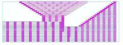
도 10a는 본 발명의 일 실시예에 따른 기판 매립형 혼 안테나 구조를 3D EM 시뮬레이션 환경으로 구현한 수직 단면도.
도 10b는 본 발명의 일 실시예에 따른 기판 매립형 혼 안테나 구조를 3D EM 시뮬레이션 환경으로 구현한 평면도.
도 10c는 본 발명의 일 실시예에 따른 기판 매립형 혼 안테나 구조를 3D EM 시뮬레이션 환경으로 구현한 사시도.
도 11는 본 발명의 일 실시예에 따른 기판 매립형 혼 안테나의 반사 손실을 나타내는 도면.
도 12a는 본 발명의 일 실시예에 따른 기판 매립형 혼 안테나의 60GHz 주파수에서 E 플레인 방사 패턴을 나타내는 도면.
도 12b는 본 발명의 일 실시예에 따른 기판 매립형 혼 안테나의 60GHz 주파수에서 H 플레인 방사 패턴을 나타내는 도면.
도 12c는 본 발명의 일 실시예에 따른 기판 매립형 혼 안테나의 60GHz 주파수에서 측면의 3D 빔 패턴을 나타내는 도면.
도 13a는 본 발명의 또 다른 실시예에 따른 기판 매립형 수직 방사 안테나와 수평 방사 안테나의 구조를 3D EM 시뮬레이션 환경으로 구현한 수직 단면도.
도 13b는 본 발명의 또 다른 실시예에 따른 기판 매립형 수직 방사 안테나와 수평 방사 안테나의 구조를 3D EM 시뮬레이션 환경으로 구현한 평면도.
도 13c는 본 발명의 또 다른 실시예에 따른 기판 매립형 수직 방사 안테나와 수평 방사 안테나의 구조를 3D EM 시뮬레이션 환경으로 구현한 사시도.
도 14a는 본 발명의 또 다른 실시예에 따른 수평 방사와 수직 방사의 선택적 이용이 가능한 기판 매립형 혼 안테나의 수직 방사를 선택하여 신호를 인가했을 때 생성되는 수직 방향의 빔 패턴 도면.
도 14b는 본 발명의 또 다른 실시예에 따른 수평 방사와 수직 방사의 선택적 이용이 가능한 기판 매립형 혼 안테나의 수평 방사를 선택하여 신호를 인가했을 때 생성되는 수직 방향의 빔 패턴 도면.1A is a diagram illustrating a transmission method using a horizontal radiation pattern of a mobile terminal and a high-performance display device.
1B illustrates a transmission scheme using a vertical radiation pattern of a mobile terminal and a high-performance display device.
1C is a diagram illustrating a transmission method using a horizontal radiation pattern in a chip-to-chip communication on the same board.
1D is a diagram illustrating a transmission method using a vertical radiation pattern between boards.
1e shows a horn antenna and radiation in a horizontal direction;
1F shows a horn antenna and radiation in a vertical direction;
FIG. 2A is a perspective view illustrating a substrate-embedded horn antenna according to an embodiment of the present invention; FIG.
FIG. 2B is a sectional view of a substrate-embedded horn antenna according to an embodiment of the present invention; FIG.
FIG. 3A is a detailed view showing a structure of a power feeding part and a direction of an electric field of a substrate-embedded horn antenna according to an embodiment of the present invention; FIG.
FIG. 3B is a cross-sectional view of a substrate-embedded horn antenna according to an embodiment of the present invention; FIG.
4 is a wire bonding connection of a substrate-embedded horn antenna and an integrated circuit according to an embodiment of the present invention.
5 illustrates a flip chip bonding connection of a substrate-embedded horn antenna and an integrated circuit in accordance with an embodiment of the present invention.
6A is a perspective view showing a substrate-embedded vertical radiation antenna and a horizontal radiation antenna according to another embodiment of the present invention.
FIG. 6B is a diagram illustrating a switch connection of a substrate-embedded vertical radiation antenna and a horizontal radiation antenna according to another embodiment of the present invention; FIG.
6C is a diagram illustrating a method of feeding a substrate-embedded vertical radiation antenna and a horizontal radiation antenna according to another embodiment of the present invention.
FIG. 7A is a view illustrating a substrate-embedded antenna and a switch connection capable of selecting and radiating four directions of a top surface, a front surface, a left surface, and a right surface according to another embodiment of the present invention. FIG.
FIG. 7B is a view illustrating a method of feeding a substrate-embedded antenna capable of radiating four directions of a top surface, a front surface, a left surface, and a right surface in accordance with another embodiment of the present invention.
8 illustrates a substrate-embedded horn antenna with a plurality of horizontal emissions and a substrate-embedded horn antenna with a plurality of vertical emissions according to another embodiment of the present invention.
FIG. 9 illustrates a beamformer constructed by connecting a phase-shifter to a substrate-embedded horn antenna having a plurality of horizontal radiation and a substrate-embedded horn antenna having a plurality of vertical radiation according to another embodiment of the present invention.
FIG. 10A is a vertical cross-sectional view illustrating a substrate-embedded horn antenna structure according to an embodiment of the present invention in a 3D EM simulation environment. FIG.
FIG. 10B is a plan view illustrating a substrate-embedded horn antenna structure according to an embodiment of the present invention in a 3D EM simulation environment. FIG.
FIG. 10C is a perspective view of a board-embedded horn antenna structure according to an embodiment of the present invention implemented in a 3D EM simulation environment. FIG.
11 is a view showing return loss of a substrate-embedded horn antenna according to an embodiment of the present invention.
12A is a diagram illustrating an E-plane emission pattern at a 60 GHz frequency of a substrate-embedded horn antenna according to an embodiment of the present invention.
12B shows an H plane emission pattern at a 60 GHz frequency of a substrate-embedded horn antenna according to an embodiment of the present invention.
12C is a diagram illustrating a 3D beam pattern of a side at a 60 GHz frequency of a substrate-embedded horn antenna according to an embodiment of the present invention.
13A is a vertical cross-sectional view illustrating a structure of a substrate-embedded vertical radiation antenna and a horizontal radiation antenna according to another embodiment of the present invention in a 3D EM simulation environment.
FIG. 13B is a plan view illustrating a structure of a substrate-embedded vertical radiation antenna and a horizontal radiation antenna according to another embodiment of the present invention in a 3D EM simulation environment. FIG.
13C is a perspective view illustrating a structure of a substrate-embedded vertical radiation antenna and a horizontal radiation antenna according to another embodiment of the present invention in a 3D EM simulation environment.
FIG. 14A is a vertical beam pattern diagram generated when a signal is applied by selecting vertical radiation of a substrate-embedded horn antenna capable of selectively using horizontal radiation and vertical radiation according to another embodiment of the present invention; FIG.
FIG. 14B is a view of a vertical beam pattern generated when a signal is applied by selecting a horizontal radiation of a substrate-embedded horn antenna capable of selectively using horizontal radiation and vertical radiation according to another embodiment of the present invention. FIG.
이하 본 발명의 실시를 위한 구체적인 실시예를 도면을 참고하여 설명한다. 예시된 도면은 발명의 명확성을 위하여 핵심적인 내용만 확대 도시하고 부수적인 것은 생략하였으므로 도면에 한정하여 해석하여서는 아니 된다.
Hereinafter, embodiments of the present invention will be described with reference to the drawings. The drawings illustrate only the essential features for the sake of clarity of the invention and are not to be construed as limiting the drawings.
도 2a는 본 발명의 일 실시예에 따른 기판 매립형 혼 안테나를 나타낸 사시도이며 도 2b는 본 발명의 일 실시예에 따른 기판 매립형 혼 안테나의 단면도로서, 기판 매립형 혼 안테나는 유전체, 금속 패턴, 금속 비아, 접지면을 포함할 수 있다.FIG. 2A is a perspective view of a board-embedded horn antenna according to an embodiment of the present invention, FIG. 2B is a sectional view of a board-embedded horn antenna according to an embodiment of the present invention, , And a ground plane.
복수의 금속 패턴(710)은 중공된 사각 또는 원형의 형상으로 유전체 내부에 적층되어 매립된다. 상기 복수의 금속 패턴(710)은 방사형으로 적층되어 전자기파가 집중되어 전파되는 웨이브가이드 구조를 형성할 수 있다.The plurality of
복수의 금속 비아(720)는 상기 금속 패턴(710)의 층간에 매립되어 상하로 연결하고 접지면은 상기 유전체의 상부에 형성된다.A plurality of
유전체 기판의 적층 구조를 활용하고 금속 패턴(710)과 금속 비아(720)를 적절히 배치하여 이를 접지면과 연결하여 전자기파가 집중되어 전파되는 일반 사각 웨이브가이드와 같은 구조를 만들어 혼 안테나의 동작 원리로 전자기파를 공기 중으로 방사하게 된다.
By using the laminated structure of the dielectric substrate and arranging the
보다 구체적으로 도 3a 내지 도 14b와 실시 예들을 통해 본 발명에 따른 기판 매립형 혼 안테나를 설명하면 다음과 같다More specifically, a substrate-embedded horn antenna according to the present invention will be described with reference to FIGS. 3A to 14B and embodiments
제11st실시예Example
도 3a는 본 발명의 일 실시예에 따른 기판 매립형 혼 안테나의 급전 부분의 구조와 전기장의 방향을 나타낸 상세 도면으로서, 기판 매립형 혼 안테나는 급전 선로, 공진 선로, 비아를 더 포함할 수 있다.FIG. 3A is a detailed view illustrating the structure of a feed portion and the direction of an electric field of a substrate-embedded horn antenna according to an embodiment of the present invention. The substrate-embedded horn antenna may further include a feed line, a resonant line, and a via.
급전 선로(910)는 상기 유전체 상부에 위치하되 상기 접지면과 이격되어 형성되고, 공진 선로(930)는 상기 금속 패턴의 최상층에 연결되고 급전 신호 파장의 λ/4의 길이를 갖는다.The
비아(920)는 급전 선로(910) 및 공진 선로를 연결하여 기판상에 구현된 웨이브가이드(940)로 급전하여 TEM 모드 전송 선로에서 TE01 모드로 변환하여 신호가 인가될 수 있다.The via 920 couples the
마이크로스트립 혹은 코플라나웨이브가이드(910)과 같은 급전 선로에 금속 비아(920)와 4분의 1파장 길이의 공진 선로(930)를 연결하여 기판상에 구현된 사각 웨이브가이드(940)로 급전을 하는 구조이다. 급전이 되는 사각 웨이브가이드의 가로 길이는 원하는 주파수의 반 파장 크기를 갖는다. 이렇게 구성된 급전 선로는 마이크로스트립 혹은 코플라나웨이브가이드와 같은 선로(910)의 전송 모드인 TEM 모드에서 사각 웨이브가이드(940)의 기본 모드인 TE01 모드로 원할한 신호 전환이 이뤄저 손실 없이 신호가 인가될 수 있다.The
도 3b는 본 발명의 일 실시예에 따른 기판 매립형 혼 안테나의 단면도로서 전기장의 변화 흐름을 표시하였다. 사각 웨이브가이드 역할을 하는 금속 패턴(1010)은 접지면와 연결된 상태로 4분의 1파장 길이의 공진 선로(1020)를 통해 무한 크기의 임피던스 상태로 변환 되고 이 때 전기장의 방사가 가장 크게 나타게 된다. 공진 선로(1020)의 끝 지점에서 방사된 전기장(화살표로 도시 1030)은 점차 커지는 사각 웨이브가이드의 금속 패턴을 따라 아래로 이동하게 되어 결국 사각 웨이브 가이드의 기본 모드인 TE01 모드로 변환되어 공기로 방사되게 된다.FIG. 3B is a cross-sectional view of a substrate-embedded horn antenna according to an embodiment of the present invention. The
도 4는 본 발명의 일 실시예에 따른 기판 매립형 혼 안테나와 집적회로의 와이어 본딩 연결을 나타낸 도면로서, 기판 매립형 혼 안테나는 송수신 집적회로 칩을 포함할 수 있다.FIG. 4 illustrates a wire bonding connection between a substrate-embedded horn antenna and an integrated circuit according to an embodiment of the present invention. The substrate-embedded horn antenna may include a transmission / reception integrated circuit chip.
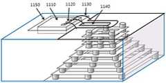
송수신 집적회로 칩은 상기 유전체의 상부에 위치하되 상기 접지면과 수평으로 이격되어 실장된다. 송수신 집적회로(1110)의 접지패드와 상기 접지면이 와이어 본딩(1130)으로 연결되고, 상기 송수신 집적회로(1110) 칩의 신호패드와 상기 급전 선로가 와이어 본딩(1130)으로 연결되되, 상기 송수신 집적회로(1110)는 상기 유전체에 형성된 캐비티에 실장되어 신호 전달 거리가 짧을 수 있다.The transmitting / receiving integrated circuit chip is mounted on the dielectric layer and horizontally spaced from the ground plane. The ground pad of the transmission / reception integrated
송수신 집적회로(1110)의 접지면-신호-접지면 패드(1120)에서 시작된 와이어 본딩(1130)은 안테나의 급전 시작인 기판 상의 코플라나 웨이브가이드 선로의 접지면-신호-접지면의 금속 패턴(1140)으로 연결되어 집적회로로부터 신호가 전달된다. 이 때 신호 전달의 거리를 짧게 하여 손실을 줄이기 위해 캐비티(1150) 구조를 활용하여 집적회로를 기판 안에 넣어 연결할 수 있다.The
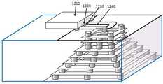
도 5는 본 발명의 일 실시예에 따른 기판 매립형 혼 안테나와 집적회로의 플립칩 본딩 연결을 나타낸 도면로서, 기판 매립형 혼 안테나는 플립칩 본딩 연결된 송수신 집적회로 칩을 포함할 수 있다.FIG. 5 illustrates a flip chip bonding connection of a substrate-embedded horn antenna and an integrated circuit according to an embodiment of the present invention. The substrate-embedded horn antenna may include a transmission / reception integrated circuit chip connected by flip-chip bonding.
송수신 집적회로(1210) 칩은 상기 접지면의 상부에 위치하되 송수신 집적회로 칩의 접지 패드와 신호 패드가 형성된 면이 하부에 놓여 있는 형상으로 위치한다.The transmitting / receiving
상기 접지 패드와 상기 접지면이 범프로 연결되고, 상기 송수신 집적회로(1210) 칩의 신호 패드와 상기 급전 선로가 또 다른 범프로 연결될 수 있다.The ground pad and the ground plane may be connected to each other by a bump, and the signal pad of the transmission / reception integrated
송수신 집적회로(1210)의 접지면-신호-접지면 패드(1220)에서 금속 범프(1230)를 통해 기판 상의 코플라나 웨이브가이드 선로의 접지면-신호-접지면의 금속 패턴(1240)으로 연결되어 집적회로로부터 신호가 전달된다.Signal-
송수신 집적회로 칩이 실장 된 매립형 혼 안테나의 제조 방법은 금속 패턴홀 형성단계, 금속 패턴 적층 단계, 비아홀 형성 단계, 금속 수지 비아 형성 단계 및 접지면 적층 단계를 포함할 수 있다.The manufacturing method of the buried horn antenna in which the transmitting and receiving integrated circuit chip is mounted may include a metal pattern hole forming step, a metal pattern laminating step, a via hole forming step, a metal resin via forming step, and a ground plane laminating step.
금속 패턴홀 형성 단계는 유전체를 적층하고 유전체에 금속 패턴홀을 형성하는 단계이고 금속 패턴 적층 단계는 상기 금속 패턴홀에 중공된 사각 또는 원형의 금속 패턴을 적층하는 단계이다.The metal pattern hole forming step is a step of laminating a dielectric and forming a metal pattern hole in a dielectric, and the metal pattern laminating step is a step of laminating a hollow rectangular or circular metal pattern in the metal pattern hole.
비아홀 형성 단계는 유전체를 적층하고 상기 금속 패턴의 상부에 복수개의 비아홀을 형성하는 단계이고 금속 수지 비아 형성 단계는 상기 비아홀에 금속으로 충진하여 금속 비아를 형성하는 단계이다.The step of forming a via hole is a step of laminating a dielectric and forming a plurality of via holes on the metal pattern. In the step of forming a metal resin via, the via hole is filled with a metal to form a metal via.
위의 단계를를 포함하여 반복하되 상기 금속 패턴은 방사형으로 적층하고 상기 유전체 상부에 접지면을 적층할 수 있다.The above steps may be repeated including the step of laminating the metal pattern radially and laminating the ground plane on the dielectric.
송수신 집적회로 칩이 실장 된 매립형 혼 안테나의 제조 방법은 공진 선로 적층 단계, 비아홀 형성 단계, 급전 선로 적층 단계를 더 포함할 수 있다.The manufacturing method of the buried horn antenna in which the transmitting / receiving integrated circuit chip is mounted may further include a resonant line laminating step, a via hole forming step, and a feed line laminating step.
공진 선로 적층 단계는 최상층의 상기 금속 패턴에 연결되는 공진 선로를 적층하는 단계이고 비아홀 형성 단계는 유전체를 적층하고 상기 공진 선로의 상부에 비아홀을 형성하는 단계이다. 급전 선로 적층 단계는 상기 유전체 상부에 위치하되 상기 접지면과 이격되고 상기 비아홀과 연결되는 급전 선로를 적층하는 단계이다.The resonant line laminating step is a step of laminating a resonant line connected to the metal pattern of the uppermost layer, and the via hole forming step is a step of laminating a dielectric and forming a via hole on the resonant line. The feeder line stacking step is a step of stacking a feeder line located on the dielectric and spaced apart from the ground plane and connected to the via hole.
또한, 수신 집적회로 칩이 실장 된 매립형 혼 안테나의 제조 방법은 집적회로 칩 실장 단계 및 와이어 본딩 연결 단계를 더 포함할 수 있다.The manufacturing method of the buried horn antenna in which the receiving integrated circuit chip is mounted may further include an integrated circuit chip mounting step and a wire bonding connecting step.
송수신 집적회로 칩 실장 단계는 상기 접지면과 수평으로 이격된 상기 유전체의 상부에 캐비티를 형성하고 캐비티에 송수신 집적회로의 칩을 실장하는 단계이고 와이어 본딩 연결 단계는 상기 송수신 집적회로의 칩의 접지 패드와 상기 접지면을 와이어 본딩으로 연결하고, 상기 송수신 집적회로 칩의 신호 패드와 상기 급전 선로가 와이어 본딩으로 연결하는 단계를 더 포함할 수 있다.Receiving integrated circuit chip mounting step includes forming a cavity on an upper portion of the dielectric horizontally spaced apart from the ground plane and mounting a chip of the transmitting / receiving integrated circuit in the cavity, and the wire bonding connecting step is a step of mounting a chip of the transmitting / And connecting the ground plane with wire bonding, and connecting the signal pad of the transmitting / receiving integrated circuit chip and the feed line by wire bonding.
더불어, 송수신 집적회로 칩이 실장 된 매립형 혼 안테나의 제조 방법은 집적회로 칩 실장 단계 및 범프 연결 단계를 더 포함할 수 있다.In addition, the manufacturing method of the buried horn antenna in which the transmitting / receiving integrated circuit chip is mounted may further include an integrated circuit chip mounting step and a bump connecting step.
송수신 집적회로 칩 실장 단계는 상기 접지면의 상부에 송수신 집적회로의 칩을 실장하는 단계이고 범프 연결 단계는 상기 송수신 집적회로 칩의 접지 패드와 신호 패드가 형성된 면을 하부에 놓고, 상기 접지 패드와 상기 접지면을 범프로 연결하고, 상기 송수신 집적회로 칩의 신호 패드와 상기 급전 선로가 또 다른 범프로 연결하는 단계를 더 포함할 수 있다.Receiving integrated circuit chip mounting step is a step of mounting a chip of the transmitting / receiving integrated circuit on the ground plane, and the bump connecting step is a step of placing the ground pad of the transmitting / receiving integrated circuit chip and the signal pad on a lower surface, Connecting the ground plane with a bump, and connecting the signal pad of the transmitting / receiving integrated circuit chip and the feed line to another bump.
제2Second실시예Example
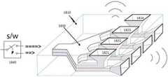
도 6a은 본 발명의 또 다른 실시예에 따른 기판 매립형 수직 방사 안테나와 수평 방사 안테나를 나타내는 사시도로서, 본 발명에서 가장 핵심이 되는 수평 방사(1310)와 수직 방사(1320)의 선택적 이용이 가능하게 하는 구조의 배경이 되는 두 가지 방사를 갖는 기판 매립형 혼 안테나를 하나의 기판에 집적하는 방법을 나타내는 도면이다. 수평 방사와 수직 방사의 선택적 이용이 가능한 매립형 혼 안테나는 웨이브가이드 구조를 형성하는 혼 안테나를 기판에 수직 매립하고 수직 안테나와 동일 기판에 수평 매립함으로써 선택적 이용이 가능하다.FIG. 6A is a perspective view illustrating a substrate-embedded vertical radiation antenna and a horizontal radiation antenna according to another embodiment of the present invention. In FIG. 6A, the
유전체, 상기 유전체 내부에 적층되어 매립되는 중공된 사각 또는 원형의 복수의 금속 패턴, 상기 금속 패턴의 층간에 매립되어 상하로 연결하는 복수의 금속 비아 및 상기 유전체의 상부에 형성된 접지면을 포함하며 상기 복수의 금속 패턴은 방사형으로 적층되어 전자기파가 집중되어 전파되는 웨이브가이드 구조를 형성하는 혼 안테나에 있어서, 기판에 수직 매립되는 혼 안테나(1410) 및 상기 수직 매립 혼 안테나와 동일 기판에 수평 매립되는 혼 안테나(1420)를 포함하여 수평 방사와 수직 방사를 선택적으로 이용할 수 있다. 수직 방사 역할을 하는 수직 매립형 혼 안테나(1410)와 수평 방사 역할을 하는 수평 매립형 혼 안테나(1420)를 하나의 기판(1430)에 적층 구조를 활용하여 구현할 수 있다. 각 안테나는 도 2a의 기판 매립형 혼 안테나 구조를 활용하였고 금속 패턴과 금속 비아로 이뤄져 개별 혼 안테나로 동작하고 있다. 각 안테나의 신호 인가 방식은 기판 내부에 구현이 가능하고 손실이 적으며 적층 구조를 활용한 신호선 분리가 용이한 스트립 선로 구조(1440)로 연결되어 있다.And a plurality of metal vias embedded between the layers of the metal pattern and vertically connected to each other, and a ground plane formed on the dielectric layer, wherein the plurality of metal vias are embedded in the dielectric layer, A horn antenna for forming a waveguide structure in which a plurality of metal patterns are laminated in a radial manner and electromagnetic waves are concentrated and propagated, the horn antenna comprising: a horn antenna (1410) vertically embedded in a substrate; and a horn Horizontal and vertical radiation, including
또한 도 6b는 본 발명의 또 다른 실시예에 따른 기판 매립형 수직 방사 안테나와 수평 방사 안테나의 스위치 연결을 나타낸 도면이다. 수평 방사와 수직 방사의 선택적 이용이 가능한 매립형 혼 안테나는 전송 선로 및 1:2 입력 스위치를 더 포함할 수 있다.6B is a view illustrating a switch connection of a substrate-embedded vertical radiation antenna and a horizontal radiation antenna according to another embodiment of the present invention. A flip-type horn antenna capable of selective use of horizontal and vertical radiation may further include a transmission line and a 1: 2 input switch.
전송 선로는 상기 각 안테나에 신호를 인가하고 1:2 입력 스위치는 상기 전송 선로의 앞단에 연결되고 상기 수직 매립 혼 안테나 및 상기 수평 매립 혼 안테나의 동작을 선택하여 수평 방사와 수직 방사의 선택적 이용이 가능하다. 수직 방향 기판 매립형 혼 안테나와 수평 방향 기판 매립형 혼 안테나의 동작을 선택하기 위한 SPDT 스위치(1450)가 스트립 전송 선로 전에 위치하게 되어 동작 선택을 하게 된다.A transmission line applies a signal to each of the antennas, a 1: 2 input switch is connected to a front end of the transmission line, and the operation of the vertical embedding horn antenna and the horizontal embedding horn antenna is selected to selectively use horizontal radiation and vertical radiation It is possible. The
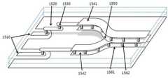
도 6c는 본 발명의 또 다른 실시예에 따른 기판 매립형 수직 방사 안테나와 수평 방사 안테나의 급전하는 방법을 나타낸 도면이다. 최초 코플라나 웨이브가이드(1510) 혹은 마이크로 스트립 선로를 이용해 신호가 인가되어 신호선(1520)과 금속 비아(1530)를 통해 각기 다른 높이의 스트립 선로1(1541), 스트립 선로2(1542)로 신호를 전달하게 된다. 각 스트립 선로는 분기점(1550)으로 모이게 되어 서로 포개어 인접하나 신호 격리가 확실한 두 스트립 선로로 수직 방사 안테나와 수평 방사 안테나로 연결되게 된다. 이 때 스트립 선로는 확실한 신호 격리를 확보할 수 있도록 위, 아래의 금속 패턴(1561)과 수직 금속 비아(1562)로 사각 웨이브가이드 형태로 구성되게 된다.6C is a diagram illustrating a method of feeding a substrate-embedded vertical radiation antenna and a horizontal radiation antenna according to another embodiment of the present invention. A signal is applied using the initial
제3Third실시예Example
도 7a는 본 발명의 또 다른 실시예에 따른 상면, 정면, 좌면, 우면의 네 방향을 선택하여 방사할 수 있는 기판 매립형 안테나와 스위치 연결을 나타낸 도면로서, 웨이브가이드 구조를 형성하는 혼 안테나로서 세 개의 수평 매립 혼 안테나 및 한개의 수직 매립 혼 안테나를 포함하여 상면, 정면, 좌면, 우면 방향의 방사의 선택적 이용을 할 수 있다.FIG. 7A is a view illustrating a substrate-embedded antenna and a switch connection capable of selecting and radiating four directions of a top surface, a front surface, a left surface, and a right surface according to another embodiment of the present invention. It is possible to selectively use radiation in the top, front, left, and right directions, including the horizontal embedding horn antenna and the one vertical embedding horn antenna.
웨이브가이드 구조를 형성하는 혼 안테나는 유전체, 상기 유전체 내부에 적층되어 매립되는 중공된 사각 또는 원형의 복수의 금속 패턴, 상기 금속 패턴의 층간에 매립되어 상하로 연결하는 복수의 금속 비아 및 상기 유전체의 상부에 형성된 접지면을 포함하며, 상기 복수의 금속 패턴은 방사형으로 적층되어 전자기파가 집중되어 전파되는 웨이브가이드 구조를 형성할 수 있다.The horn antenna forming the waveguide structure includes a dielectric, a plurality of hollow square or circular metal patterns stacked and buried in the dielectric, a plurality of metal vias embedded in the upper and lower portions of the metal pattern, And a plurality of metal patterns are stacked in a radial manner to form a waveguide structure in which electromagnetic waves are concentrated and propagated.
세 개의 수평 매립 혼 안테나는 기판의 동일층에 정면, 좌면, 우면 방향으로 배열되고 수직 매립 혼 안테나는 상기 수평 매립 혼 안테나와 동일 기판에 상면 방향으로 배열되어 상면, 정면, 좌면, 우면의 네 방향 방사의 선택적 이용을 할 수 있다.The three horizontal embedding horn antennas are arranged in the same layer of the substrate in front, left, and right directions, and the vertical embedding horn antennas are arranged on the same substrate as the horizontally embedded horn antennas in the top surface, It is possible to selectively use radiation.
기판 매립형 안테나는 전송 선로 및 1:4 입력 스위치를 포함하여 안테나 동작을 선택할 수 있다. 전송 선로는 상기 각 안테나에 신호를 인가하고 1:4 입력 스위치는 상기 전송 선로의 앞단에 연결되고 상기 수직 매립 혼 안테나 및 상기 수평 매립 혼 안테나의 동작을 선택하여 상면, 정면, 좌면, 우면의 네 방향 방사의 선택적 이용을 할 수 있다.The board-buried antenna may include an antenna operation including a transmission line and a 1: 4 input switch. A transmission line applies a signal to each of the antennas, a 1: 4 input switch is connected to a front end of the transmission line, selects an operation of the vertical embedding horn antenna and the horizontal embedding horn antenna, Directional radiation can be selectively used.
이는 단일 기판 매립형 혼 안테나를 활용하여 하나의 기판 상에 각기 다른 네 가지 방향의 방사 패턴을 갖고 이를 선택하여 이용할 수 있는 다방향 선택이 가능한 기판 매립형 혼 안테나를 구현한 것이다. 도 6b의 수직 방사와 수평 방사의 선택이 가능한 혼 안테나 구조에 양 옆면(1610, 1620)에 추가로 기판 매립형 혼 안테나를 삽입하여 앞, 상, 좌, 우의 네 면을 모두 활용해 초소형 구조로 다방향 방사가 가능하게 하였다. 각 기판 매립형 혼 안테나는 도 2a의 단일 기판 매립형 혼 안테나와 같은 금속 패턴과 금속 비아로 이뤄져 있으며, 신호 인가는 확실한 신호 격리 특성과 적은 손실로 기판에 실장 가능한 스트립 선로(1630)으로 연결되어 있다. 각 방사 방향을 선택적으로 이용 가능하게 하도록 네 가지 스트립 선로(1630)에 SP4T 스위치(1640)가 연결되어 동작된다.In this paper, we propose a multi - directional substrate - horn antenna using a single - substrate embedded horn antenna with four different radiation patterns on a single substrate. 6B, a substrate-embedded horn antenna is inserted into both
도 7b는 본 발명의 또 다른 실시예에 따른 상면, 정면, 좌면, 우면의 네 방향을 선택하여 방사할 수 있는 기판 매립형 안테나의 급전하는 방법을 나타내는 도면으로서 네 가지 방향에 각각 다른 신호의 급전을 위해 최초 네 개의 코플라나 웨이브가이드(1710) 혹은 마이크로 스트립 선로를 이용해 신호가 인가되어 신호선(1720)과 금속 비아(1730)를 통해 각기 다른 높이의 스트립 선로1(1741), 스트립 선로2(1742), 스트립 선로3(1743), 스트립 선로4(1744)로 신호를 전달하게 된다. 정면과 수직 방사를 위한 스트립 선로는 분기점(1750)으로 모이게 되어 서로 포개어 인접하나 신호 격리가 확실한 두 스트립 선로로 수직 방사 안테나와 수평 방사 안테나로 연결 되게 되고, 좌, 우 방향의 방사를 위한 스트립 선로(1743, 1744)들은 개별 연결로 신호 격리을 유지한 상태로 각 안테나로 연결된다. 이때 스트립 선로는 확실한 신호 격리을 확보할 수 있도록 위, 아래의 금속 패턴(1761)과 수직 금속 비아(1762)로 사각 웨이브가이드 형태로 구성되게 된다FIG. 7B is a diagram illustrating a method of feeding a substrate-embedded antenna capable of radiating four directions of a top surface, a front surface, a left surface, and a right surface in accordance with another embodiment of the present invention, A signal is applied using the first four
제4Fourth실시예Example
도 8은 본 발명의 또 다른 실시예에 따른 복수의 수평 방사를 갖는 기판 매립형 혼 안테나와 복수의 수직 방사를 갖는 기판 매립형 혼 안테나를 나타내는 도면으로서 웨이브가이드 구조를 형성하는 혼 안테나로서 복수의 수평 매립 혼 안테나, 복수의 수직 매립 혼 안테나 및 전력 분배기 또는 전력 결합기를 더 포함할 수 있다.8 is a view of a substrate-embedded horn antenna with a plurality of horizontal emissions and a substrate-embedded horn antenna with a plurality of vertical emissions according to another embodiment of the present invention, Horn antenna, a plurality of vertically embedding horn antennas, and a power divider or power combiner.
웨이브가이드 구조를 형성하는 혼 안테나는 유전체, 상기 유전체 내부에 적층되어 매립되는 중공된 사각 또는 원형의 복수의 금속 패턴, 상기 금속 패턴의 층간에 매립되어 상하로 연결하는 복수의 금속 비아 및 상기 유전체의 상부에 형성된 접지면을 포함하며, 상기 복수의 금속 패턴은 방사형으로 적층되어 전자기파가 집중되어 전파되는 웨이브가이드 구조를 형성할 수 있다.The horn antenna forming the waveguide structure includes a dielectric, a plurality of hollow square or circular metal patterns stacked and buried in the dielectric, a plurality of metal vias embedded in the upper and lower portions of the metal pattern, And a plurality of metal patterns are stacked in a radial manner to form a waveguide structure in which electromagnetic waves are concentrated and propagated.
복수의 수평 매립 혼 안테나는 기판에 동일층에 정면 방향으로 배열되고 복수의 수직 매립 혼 안테나는 상기 수평 매립 혼 안테나와 동일 기판에 상면 방향으로 배열될 수 있다. 전력 분배기는 송신기를 구현하도록 각 안테나에 일정비율로 전력을 분배하고 전력 결합기는 수신기를 구현하도록 각 안테나에 수신된 전력을 결합하는 것으로 용도에 따라 선택하여 포함할 수 있다.The plurality of horizontally embedded horn antennas may be arranged on the same layer in the front direction on the substrate and the plurality of vertically embedding horn antennas may be arranged on the same substrate as the horizontal embedding horn antenna in the upper surface direction. The power divider may selectively distribute the power to each antenna at a certain rate to implement the transmitter and the power combiner may select and combine the received power to each antenna to implement the receiver.
매립형 혼 안테나는 1:2 입력 스위치를 더 포함할 수 있다. 1:2 입력 스위치는 상기 전력 분배기 또는 상기 전력 결합기의 앞단에 연결되고 상기 수직 매립 혼 안테나 및 상기 수평 매립 혼 안테나의 동작을 선택하여 수평 방사와 수직 방사의 선택적 이용을 할 수 있다.The buried horn antenna may further include a 1: 2 input switch. The 1: 2 input switch is connected to a front end of the power divider or the power combiner and can selectively use the horizontal and vertical radiations by selecting the operation of the vertically embedded horn antenna and the horizontally embedded horn antenna.
수평 방사와 수직 방사의 선택적 이용이 가능한 기판 매립형 혼 안테나를 배열 구조화하여 하나의 기판(1810)에 구현한 것으로 배열 안테나는 더 큰 이득과 더 좁은 빔 폭이 필요한 응용 분야에 적합하며 시스템 제원에 맞게 개수를 증가하거나 줄여서 사용할 수 있다. 도 8에서는 예를 들어 4개의 배열(1821, 1822, 1823, 1824)을 제시하였지만 더 큰 이득과 더 좁은 빔 폭을 원할 경우 배열 개수를 증가하여 구성할 수 있다. 4개의 배열 안테나는 송신기로 이용할 경우 4:1 전력 분배기(1830)가 사용되게 되고 수신기로 이용할 경우 4:1 전력 결합기가 사용되어 이에 연결 되어 신호가 인가되게 된다. 도 6b와 마찬가지로 수평 방사와 수직 방사의 선택적 이용을 위해 초기에 SPDT 스위치(1840)가 연결되어 신호 선택을 하게 된다.The substrate-embedded horn antennas, which can be selectively used for horizontal and vertical radiation, are arrayed to form a
제5Fifth실시예Example
도 9는 본 발명의 또 다른 실시예에 따른 복수의 수평 방사를 갖는 기판 매립형 혼 안테나와 복수의 수직 방사를 갖는 기판 매립형 혼 안테나에 위상 변환기를 연결하여 빔 형성기를 구성한 도면으로서 웨이브가이드 구조를 형성하는 혼 안테나로서 복수의 수평 매립 혼 안테나, 복수의 수직 매립 혼 안테나 및 위상 변환기를 더 포함할 수 있다.FIG. 9 is a view illustrating a beam former by connecting a phase-shifter to a substrate-embedded horn antenna having a plurality of horizontal radiation and a substrate-embedded horn antenna having a plurality of vertical radiation according to another embodiment of the present invention. The horn antenna may further include a plurality of horizontal embedding horn antennas, a plurality of vertical embedding horn antennas, and a phase shifter.
웨이브가이드 구조를 형성하는 혼 안테나는 유전체, 상기 유전체 내부에 적층되어 매립되는 중공된 사각 또는 원형의 복수의 금속 패턴, 상기 금속 패턴의 층간에 매립되어 상하로 연결하는 복수의 금속 비아 및 상기 유전체의 상부에 형성된 접지면을 포함하며, 상기 복수의 금속 패턴은 방사형으로 적층되어 전자기파가 집중되어 전파되는 웨이브가이드 구조를 형성할 수 있다.The horn antenna forming the waveguide structure includes a dielectric, a plurality of hollow square or circular metal patterns stacked and buried in the dielectric, a plurality of metal vias embedded in the upper and lower portions of the metal pattern, And a plurality of metal patterns are stacked in a radial manner to form a waveguide structure in which electromagnetic waves are concentrated and propagated.
복수의 수평 매립 혼 안테나는 기판에 동일층에 정면 방향으로 배열되고, 복수의 수직 매립 혼 안테나는 상기 수평 매립 혼 안테나와 동일 기판에 상면 방향으로 배열될 수 있다. 위상 변환기는 각 안테나로 들어가는 위상을 변화시켜 수직 방향과 수평 방향의 빔의 방향을 조절하는 빔 형성기를 구현할 수 있다.The plurality of horizontally embedded horn antennas may be arranged on the same layer in the front direction on the substrate, and the plurality of vertically embedding horn antennas may be arranged on the same substrate as the horizontal embedding horn antenna in the top surface direction. The phase shifter can implement a beamformer that adjusts the direction of the beam in the vertical and horizontal directions by changing the phase entering each antenna.
매립형 혼 안테나는 1:2 입력 스위치를 더 포함할 수 있다. 1:2 입력 스위치는 상기 위상 변환기의 앞단에 연결되고 수직 방향과 수평 방향을 선택하여 수평 방사와 수직 방사의 선택적 이용을 할 수 있다.The buried horn antenna may further include a 1: 2 input switch. The 1: 2 input switch is connected to the front end of the phase shifter and can select vertical and horizontal directions to selectively use horizontal and vertical radiation.
도 9는 도 8에서 나타낸 수평 방사와 수직 방사의 선택적 이용이 가능한 기판 매립형 배열 혼 안테나 구조에서 전력 분배기 대신 위상 변환기를 삽입하여 각 안테나로 들어가는 위상을 변화 시켜 빔 형성기를 구현하는 도면이다. 4개의 수직 안테나(1911, 1912, 1913, 1914)에 각각 위상 변환기(1920)를 연결하였으며, 마찬가지로 4개의 수평 안테나(1931, 1932, 1933, 1934)에 각각 위상 변환기(1920)를 연결해 수직 방향의 빔과 수평 방향의 빔의 방향을 조절할 수 있다. 이때 입력 부분에는 수직 방향과 수평 방향을 선택할 수 있는 SPDT 스위치(1940)가 연결되어 동작하게 된다.FIG. 9 is a view illustrating the implementation of a beam former by inserting a phase shifter instead of a power divider in a substrate-embedded array horn antenna structure capable of selectively using the horizontal radiation and the vertical radiation shown in FIG. A
도 10은 본 발명의 일 실시예에 따른 기판 매립형 혼 안테나 구조를 3D EM 시뮬레이션 환경으로 구현한 도면이고, 도 11은 본 발명의 일 실시예에 따른 기판 매립형 혼 안테나의 반사 손실을 나타내는 도면이고, 도 12는 본 발명의 일 실시예에 따른 기판 매립형 혼 안테나의 60GHz 주파수에서 방사 및 3D 빔 패턴을 나타내는 도면이다.FIG. 10 is a diagram illustrating a structure of a substrate-embedded horn antenna according to an embodiment of the present invention in a 3D EM simulation environment, FIG. 11 is a view illustrating return loss of a substrate-embedded horn antenna according to an embodiment of the present invention, 12 is a diagram illustrating a radiation and 3D beam pattern at a 60 GHz frequency of a substrate-embedded horn antenna according to an embodiment of the present invention.
도 11, 도 12a, 도 12b 및 도 12c 는 본 발명에서 제안하는 단일 기판 매립형 혼 안테나의 구조의 동작 특성을 나타낸다. 도 10a, 도10b, 도10c의 시뮬레이션 환경에서 확인하였으며 실시 예로 구현의 가능성을 설명하고자 시뮬레이션 결과를 삽입하였다. 이때 유전체 기판은 LTCC기판 (Low Temperature Co-fired Ceramic)을 이용하여 유전율(dielectric constant)은 5.9, 유전손실(loss tangent)은 0.0035의 조건을 활용하였으며 metal의 물질은 은(Ag)을 사용하여 구성하였다.FIGS. 11, 12A, 12B, and 12C show the operation characteristics of the structure of the single substrate embedded horn antenna proposed in the present invention. 10a, 10b, and 10c, and simulation results are inserted to illustrate the feasibility of the embodiment. The dielectric constant of the dielectric substrate was 5.9 and the loss tangent of 0.0035 was used for the LTCC substrate (Low Temperature Co-fired Ceramic). The metal material was composed of silver (Ag) Respectively.
설계된 구조의 크기는 매립형 혼 안테나 개구면의 경우 가로 3.4mm, 세로 2.4mm이고, CMOS칩이 포함된 전체 기판의 크기는 가로 4.5mm, 세로 5mm, 높이 0.85mm로 설계하였다.The size of the designed structure is 3.4mm in width and 2.4mm in length in the open horn antenna. The size of the whole board including CMOS chip is 4.5mm, 5mm, and 0.85mm.
본 실시예의 결과는 LTCC 기판의 특성을 활용하여 설계하였지만 평면 기판의 성격을 갖는 다양한 기판 (PCB, Duroid, Taconic, Ceramic 등)에 적용 가능하다.The results of this embodiment are applicable to various substrates (PCB, Duroid, Taconic, Ceramic, etc.) which are designed by utilizing the characteristics of the LTCC substrate but have the characteristics of a flat substrate.
도 11은 삽입 손실을 나타내고 있으며 -10dB 아래의 주파수 폭이 53GHz에서 66GHz로 13GHz 대역을 만족하고 있다.11 shows the insertion loss, and the frequency width below -10 dB satisfies the 13 GHz band from 53 GHz to 66 GHz.
도 12a는 E 플레인 상의 빔 패턴을 나타내고 있고 Maximum gain은 7.35dBi, HPBW(Half Power Beam Width)는 60°(±30°)를 갖는다.12A shows a beam pattern on the E plane, with a maximum gain of 7.35 dBi and a HPBW (Half Power Beam Width) of 60 DEG (+/- 30 DEG).
도 12b는 H 플레인 상의 빔 패턴을 나타내고 있으며 Maxium gain은 7.35dBi. HPBW는 70°(±35°)를 갖는다.FIG. 12B shows the beam pattern on the H plane and the Maxium gain is 7.35 dBi. HPBW has 70 占 (占 0 占.
도 12c는 전체 빔 패턴의 입체 모양에서 측면 부분을 표시하였다.
FIG. 12C shows the side portion in the solid shape of the entire beam pattern.
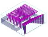
도 13은 본 발명의 또 다른 실시예에 따른 수직 방사 안테나와 수평 방사 안테나를 한 기판에 구현하여 수평 방사와 수직 방사의 선택적 이용이 가능한 안테나의 구조를 3D EM 시뮬레이션 환경으로 구현한 도면이고, 도 14는 본 안테나의 수직 방사와 수평 방사를 선택하여 신호를 인가했을 때 생성되는 빔 패턴 도면이다.13 is a diagram illustrating a structure of an antenna capable of selectively using horizontal radiation and vertical radiation in a 3D EM simulation environment by implementing a vertical radiation antenna and a horizontal radiation antenna according to another embodiment of the present invention on one substrate, 14 is a beam pattern diagram generated when a vertical emission and a horizontal emission of the antenna are selected and a signal is applied.
도 14a 및 도 14b는 본 발명에서 제안하는 수평 방사와 수직 방사의 선택적 이용이 가능한 기판 매립형 혼 안테나 구조의 동작 특성을 나타낸다. 도 13a 내지 도 13c의 시뮬레이션 환경에서 확인하였으며 실시 예로 구현의 가능성을 설명하고자 시뮬레이션 결과를 삽입하였다. 이때 유전체 기판은 LTCC기판 (Low Temperature Co-fired Ceramic)을 이용하여 유전율(dielectric constant)은 5.9, 유전손실(loss tangent)은 0.0035의 조건을 활용하였으며 metal의 물질은 은(Ag)을 사용하여 구성하였다.FIGS. 14A and 14B show operating characteristics of a substrate-embedded horn antenna structure capable of selectively using the horizontal radiation and the vertical radiation proposed in the present invention. 13A to 13C, and simulation results are inserted to illustrate the feasibility of implementation in the embodiment. The dielectric constant of the dielectric substrate was 5.9 and the loss tangent of 0.0035 was used for the LTCC substrate (Low Temperature Co-fired Ceramic). The metal material was composed of silver (Ag) Respectively.
설계된 구조의 크기는 매립형 혼 안테나 개구면의 경우 수직 방사 안테나는 가로 3.9mm, 세로 2.7mm이고, 수평 방사 안테나는 가로 4mm, 세로 1.5mm이며 전체 기판의 크기는 가로 4.8mm, 세로 4.6mm, 높이 1.4mm로 설계하였다. 본 발명의 가장 큰 장점인 소형화 측면에서 단일 기판 매립형 혼 안테나의 전체 크기와 비교했을 때 가로, 세로 변화는 없으며 높이가 약간 증가하였다. 이는 이동 단말기 및 칩 간 통신에서 민감한 가로, 세로 크기를 유지하면서 두 가지 빔 방향을 만들 수 있는 우수한 특성을 보여준다.The size of the designed structure is 3.9mm in width and 2.7mm in vertical radiation antenna, and 4mm in width and 1.5mm in vertical radiation antenna. The size of the board is 4.8mm, 4.6mm, Respectively. In terms of miniaturization, which is the greatest advantage of the present invention, there is no change in the length and length compared to the total size of the single board embedded horn antenna, and the height is slightly increased. This shows excellent characteristics of making two beam directions while maintaining a sensitive horizontal and vertical size in mobile terminal and inter-chip communication.
본 실시예의 결과는 LTCC 기판의 특성을 활용하여 설계하였지만 평면 기판의 성격을 갖는 다양한 기판 (PCB, Duroid, Taconic, Ceramic 등)에 적용 가능하다.The results of this embodiment are applicable to various substrates (PCB, Duroid, Taconic, Ceramic, etc.) which are designed by utilizing the characteristics of the LTCC substrate but have the characteristics of a flat substrate.
도 13a는 수평 방사와 수직 방사의 선택적 이용이 가능한 기판 매립형 혼 안테나 구조를 3D EM 시뮬레이터로 구현하여 수직 단면에서 표현한 도면이다.13A is a vertical cross-sectional view of a substrate-embedded horn antenna structure capable of selectively using horizontal radiation and vertical radiation by a 3D EM simulator.
도 13b는 수평 방사와 수직 방사의 선택적 이용이 가능한 기판 매립형 혼 안테나 구조를 3D EM 시뮬레이터로 구현하여 수평 상면에서 표현한 도면이다.FIG. 13B is a view of a substrate-embedded horn antenna structure capable of selectively using horizontal radiation and vertical radiation on a horizontal top surface by implementing a 3D EM simulator.
도 13c는 수평 방사와 수직 방사의 선택적 이용이 가능한 기판 매립형 혼 안테나 구조를 3D EM 시뮬레이터로 구현하여 수직 상측면에서 표현한 도면이다.13C is a vertical plane view of a substrate embedding type horn antenna structure capable of selectively using horizontal radiation and vertical radiation with a 3D EM simulator.
도 14a는 수직 방사를 선택하여 신호를 인가하였을 때 나타나는 기판의 수직 방향으로 생성되는 빔 패턴이다.14A is a beam pattern generated in the vertical direction of the substrate when a vertical emission is selected and a signal is applied.
도 14b는 수평 방사를 선택하여 신호를 인가하였을 때 나타나는 기판의 수평 방향으로 생성되는 빔 패턴이다.14B is a beam pattern generated in the horizontal direction of the substrate when the horizontal emission is selected and a signal is applied.
이 결과를 보면 원하는 방향을 선택하는 대로 빔 패턴이 생성되는 것을 알 수 있고, 상, 앞, 좌, 우의 네 방향 패턴도 생성됨을 유추할 수 있다.In this result, it can be seen that the beam pattern is generated according to the selection of the desired direction, and the four direction patterns of the top, front, left, and right are also generated.
이상에서는 실시 예를 참조하여 설명하였지만, 해당 기술 분야의 숙련된 당업자는 하기의 특허 청구의 범위에 기재된 본 발명의 사상 및 영역으로부터 벗어나지 않는 범위 내에서 본 발명을 다양하게 수정 및 변경시킬 수 있음을 이해할 수 있을 것이다.It will be apparent to those skilled in the art that various modifications and variations can be made in the present invention without departing from the spirit or scope of the invention as defined in the appended claims. You will understand.
Claims (12)
Translated fromKorean상기 유전체 내부에 적층되어 매립되는 중공된 사각 또는 원형의 복수의 금속 패턴;
상기 금속 패턴의 층간에 매립되어 상하로 연결하는 복수의 금속 비아; 및
상기 유전체의 상부에 형성된 접지면을 포함하며,
상기 복수의 금속 패턴은 방사형으로 적층되어 전자기파가 집중되어 전파되는 웨이브가이드 구조를 형성하는 것을 특징으로 하는 매립형 혼 안테나.dielectric;
A plurality of hollow square or circular metal patterns stacked and embedded in the dielectric;
A plurality of metal vias embedded between the layers of the metal pattern and vertically connected to each other; And
And a ground plane formed on an upper portion of the dielectric,
Wherein the plurality of metal patterns are laminated in a radial manner to form a waveguide structure in which electromagnetic waves are concentrated and propagated.
상기 유전체 상부에 위치하되 상기 접지면과 이격되어 형성되는 급전 선로;
상기 금속 패턴의 최상층에 연결되고 급전 신호 파장의 λ/4의 길이를 갖는 공진 선로; 및
급전 선로 및 공진 선로를 연결하는 비아를 포함하여 기판상에 구현된 웨이브가이드로 급전하여 TEM 모드 전송 선로에서 TE01 모드로 변환하여 신호가 인가되는 것을 특징으로 하는 매립형 혼 안테나.The method according to claim 1,
A feed line disposed on the dielectric and spaced apart from the ground plane;
A resonance line connected to the uppermost layer of the metal pattern and having a length of? / 4 of a feed signal wavelength; And
The feed line and the resonance line are connected to each other by a waveguide formed on the substrate, and the TEM mode transmission line is converted into the TE01 mode and the signal is applied.
상기 유전체의 상부에 위치하되 상기 접지면과 수평으로 이격되어 실장되는 송수신 집적회로 칩을 포함하고, 상기 송수신 집적회로 칩의 접지패드와 상기 접지면이 와이어 본딩으로 연결되고, 상기 송수신 집적회로 칩의 신호패드와 상기 급전 선로가 와이어 본딩으로 연결되되, 상기 송수신 집적회로 칩은 상기 유전체에 형성된 캐비티에 실장된 것을 특징으로 하는 매립형 혼 안테나.3. The method of claim 2,
Receiving integrated circuit chip, wherein the ground pad and the ground plane of the transmitting / receiving integrated circuit chip are connected by wire bonding, and wherein the ground pad of the transmitting / receiving integrated circuit chip is connected by wire bonding, Wherein the signal pad and the feeding line are connected by wire bonding, and the transmitting / receiving integrated circuit chip is mounted on a cavity formed in the dielectric.
상기 접지면의 상부에 위치한 송수신 집적회로 칩을 포함하고, 상기 송수신 집적회로 칩의 접지 패드와 신호 패드가 형성된 면이 하부에 놓여 있는 형상이고, 상기 접지 패드와 상기 접지면이 범프로 연결되고, 상기 송수신 집적회로 칩의 신호 패드와 상기 급전 선로가 또 다른 범프로 연결된 것을 특징으로 하는 매립형 혼 안테나.3. The method of claim 2,
Wherein the ground pad and the ground plane are connected to each other by a bump, and the ground pad and the ground pad are connected to each other by a bump, Wherein the signal pad of the transmitting / receiving integrated circuit chip and the feeding line are connected to each other with another bump.
기판에 수직 매립되는 혼 안테나; 및
상기 수직 매립 혼 안테나와 동일 기판에 수평 매립되는 혼 안테나를 포함하는 것을 특징으로 하는 수평 방사와 수직 방사의 선택적 이용이 가능한 매립형 혼 안테나.The method of claim 1,
A horn antenna embedded perpendicularly to the substrate; And
And a horn antenna horizontally embedded in the same substrate as the vertically embedded horn antenna, wherein the horizontal horn and the vertical horn can be selectively used.
상기 각 안테나에 신호를 인가하는 전송 선로; 및
상기 전송 선로의 앞단에 연결되고 상기 수직 매립 혼 안테나와 상기 수평 매립 혼 안테나의 동작을 선택하는 1:2 입력 스위치를 포함하여 수평 방사와 수직 방사의 선택적 이용이 가능한 매립형 혼 안테나.6. The method of claim 5,
A transmission line for applying a signal to each antenna; And
And a 1: 2 input switch connected to a front end of the transmission line and selecting operation of the vertically embedded horn antenna and the horizontally embedded horn antenna, wherein the horizontal radiation and the vertical radiation can be selectively used.
기판의 동일층에 정면, 좌면, 우면 방향으로 배열되어 수평 매립되는 세 개의 혼 안테나 및
상기 수평 매립 혼 안테나와 동일 기판에 상면 방향으로 배열되어 수직 매립되는 혼 안테나를 포함하여, 상면, 정면, 좌면, 우면의 네 방향 방사의 선택적 이용이 가능한 것을 특징으로 하는 수평 방사와 수직 방사의 선택적 이용이 가능한 매립형 혼 안테나.The method according to claim 1,
Three horn antennas arranged horizontally in the front, left, and right directions on the same layer of the substrate, and
And horn antennas arranged vertically on the same substrate as the horizontally embedded horn antennas so as to be vertically embedded. The horn antennas are capable of selectively using the four directions of the top, front, left, and right sides. Embedded Horn Antenna available.
상기 각 안테나에 신호를 인가하는 전송 선로; 및
상기 전송 선로의 앞단에 연결되고 상기 수직 매립 혼 안테나와 상기 수평 매립 혼 안테나의 동작을 선택하는 1:4 입력 스위치를 포함하여 상면, 정면, 좌면, 우면의 네 방향 방사의 선택적 이용이 가능한 것을 특징으로 하는 수평 방사와 수직 방사의 선택적 이용이 가능한 매립형 혼 안테나.8. The method of claim 7,
A transmission line for applying a signal to each antenna; And
And a 1: 4 input switch connected to a front end of the transmission line and selecting the operation of the vertically-embedded horn antenna and the horizontally-embedded horn antenna, the four-directional radiation of the top, front, A horn antenna capable of selective use of horizontal radiation and vertical radiation.
기판에 정면 방향으로 배열되어 수평 매립되는 복수의 혼 안테나;
상기 수평 매립 혼 안테나와 동일 기판에 상면 방향으로 배열되어 수직 매립되는 복수의 혼 안테나 및
송신기를 구현하도록 각 안테나에 일정비율로 전력을 분배하는 전력 분배기 또는 수신기를 구현하도록 각 안테나에 수신된 전력을 결합하는 전력 결합기를 포함하는 것을 특징으로 하는 수평 방사와 수직 방사의 선택적 이용이 가능한 매립형 혼 안테나.The method according to claim 1,
A plurality of horn antennas arranged horizontally in a front direction on a substrate;
A plurality of horn antennas arranged vertically on the same substrate as the horizontally embedded horn antennas and vertically embedded;
And a power combiner for combining the power received at each antenna to implement a power divider or a receiver that distributes power at a constant rate to each antenna to implement a transmitter. ≪ RTI ID = 0.0 > Horn antenna.
상기 전력 분배기 또는 상기 전력 결합기의 앞단에 연결되고 상기 수직 매립 혼 안테나와 상기 수평 매립 혼 안테나의 동작을 선택하는 1:2 입력 스위치를 포함하는 것을 특징으로 하는 수평 방사와 수직 방사의 선택적 이용이 가능한 매립형 혼 안테나.10. The method of claim 9,
And a 1: 2 input switch connected to a front end of the power divider or the power combiner for selecting an operation of the vertically embedded horn antenna and the horizontally embedded horn antenna. Embedded Horn Antenna.
기판에 수직 매립되는 복수의 혼 안테나;
상기 수직 매립 혼 안테나와 동일 기판에 매립되되 수평 매립되는 복수의 혼 안테나 및
각 안테나로 들어가는 위상을 변화시키는 위상 변환기를 포함하여 수직 방향과 수평 방향의 빔의 방향을 조절하는 빔 형성기를 구현하는 것을 특징으로 하는 수평 방사와 수직 방사의 선택적 이용이 가능한 매립형 혼 안테나.The method according to claim 1,
A plurality of horn antennas embedded perpendicularly to the substrate;
A plurality of horn antennas embedded in the same substrate as the vertically embedded horn antennas and horizontally embedded;
And a beamformer for adjusting the directions of the beams in the vertical direction and the horizontal direction, including a phase converter for changing the phase entering each antenna, is embodied.
상기 위상 변환기의 앞단에 연결되고 수직 방향과 수평 방향을 선택하는 1:2 입력 스위치를 포함하여 수직 방향과 수평 방향의 빔의 방향을 조절하는 빔 형성기를 구현하는 것을 특징으로 하는 수평 방사와 수직 방사의 선택적 이용이 가능한 매립형 혼 안테나.12. The method of claim 11,
And a 1: 2 input switch connected to a front end of the phase shifter for selecting a vertical direction and a horizontal direction to implement a beam former for adjusting the directions of vertical and horizontal beams. Of the horn antenna.
Priority Applications (2)
| Application Number | Priority Date | Filing Date | Title |
|---|---|---|---|
| KR1020130109677AKR101454878B1 (en) | 2013-09-12 | 2013-09-12 | Subatrate Embedded Horn Antenna having Selection Capability of Vertical and Horizontal Radiation Pattern |
| US14/477,562US9716316B2 (en) | 2013-09-12 | 2014-09-04 | Substrate embedded horn antenna having selection capability of vertical and horizontal radiation pattern |
Applications Claiming Priority (1)
| Application Number | Priority Date | Filing Date | Title |
|---|---|---|---|
| KR1020130109677AKR101454878B1 (en) | 2013-09-12 | 2013-09-12 | Subatrate Embedded Horn Antenna having Selection Capability of Vertical and Horizontal Radiation Pattern |
Publications (1)
| Publication Number | Publication Date |
|---|---|
| KR101454878B1true KR101454878B1 (en) | 2014-11-04 |
Family
ID=52289031
Family Applications (1)
| Application Number | Title | Priority Date | Filing Date |
|---|---|---|---|
| KR1020130109677AExpired - Fee RelatedKR101454878B1 (en) | 2013-09-12 | 2013-09-12 | Subatrate Embedded Horn Antenna having Selection Capability of Vertical and Horizontal Radiation Pattern |
Country Status (2)
| Country | Link |
|---|---|
| US (1) | US9716316B2 (en) |
| KR (1) | KR101454878B1 (en) |
Cited By (8)
| Publication number | Priority date | Publication date | Assignee | Title |
|---|---|---|---|---|
| WO2016089597A1 (en)* | 2014-12-04 | 2016-06-09 | Qualcomm Incorporated | Cavity backed aperture antenna |
| KR101640345B1 (en)* | 2015-05-29 | 2016-07-18 | 허문만 | Antenna apparatus for portable terminal having metal case |
| WO2016133728A1 (en)* | 2015-02-20 | 2016-08-25 | Qualcomm Incorporated | Three dimensional (3d) antenna structure |
| WO2019161121A1 (en)* | 2018-02-15 | 2019-08-22 | Space Exploration Technologies Corp. | Hierarchical network signal routing apparatus and method |
| US10833414B2 (en) | 2018-03-02 | 2020-11-10 | Samsung Electro-Mechanics Co., Ltd. | Antenna apparatus and antenna module |
| US11146323B2 (en) | 2018-02-15 | 2021-10-12 | Space Exploration Technologies Corp. | Beamformer lattice for phased array antennas |
| CN113517564A (en)* | 2021-04-06 | 2021-10-19 | 浙江大学 | A CTS Beam Scanning Antenna Based on Multilayer Suspended Stripline Structure |
| US11699852B2 (en) | 2018-02-15 | 2023-07-11 | Space Exploration Technologies Corp. | Phased array antenna systems |
Families Citing this family (159)
| Publication number | Priority date | Publication date | Assignee | Title |
|---|---|---|---|---|
| US10009065B2 (en) | 2012-12-05 | 2018-06-26 | At&T Intellectual Property I, L.P. | Backhaul link for distributed antenna system |
| US9113347B2 (en) | 2012-12-05 | 2015-08-18 | At&T Intellectual Property I, Lp | Backhaul link for distributed antenna system |
| US9999038B2 (en) | 2013-05-31 | 2018-06-12 | At&T Intellectual Property I, L.P. | Remote distributed antenna system |
| US9525524B2 (en) | 2013-05-31 | 2016-12-20 | At&T Intellectual Property I, L.P. | Remote distributed antenna system |
| US9692101B2 (en) | 2014-08-26 | 2017-06-27 | At&T Intellectual Property I, L.P. | Guided wave couplers for coupling electromagnetic waves between a waveguide surface and a surface of a wire |
| US9768833B2 (en) | 2014-09-15 | 2017-09-19 | At&T Intellectual Property I, L.P. | Method and apparatus for sensing a condition in a transmission medium of electromagnetic waves |
| US10063280B2 (en) | 2014-09-17 | 2018-08-28 | At&T Intellectual Property I, L.P. | Monitoring and mitigating conditions in a communication network |
| US9615269B2 (en) | 2014-10-02 | 2017-04-04 | At&T Intellectual Property I, L.P. | Method and apparatus that provides fault tolerance in a communication network |
| US9685992B2 (en) | 2014-10-03 | 2017-06-20 | At&T Intellectual Property I, L.P. | Circuit panel network and methods thereof |
| US9503189B2 (en) | 2014-10-10 | 2016-11-22 | At&T Intellectual Property I, L.P. | Method and apparatus for arranging communication sessions in a communication system |
| US9762289B2 (en) | 2014-10-14 | 2017-09-12 | At&T Intellectual Property I, L.P. | Method and apparatus for transmitting or receiving signals in a transportation system |
| US9973299B2 (en) | 2014-10-14 | 2018-05-15 | At&T Intellectual Property I, L.P. | Method and apparatus for adjusting a mode of communication in a communication network |
| US9653770B2 (en) | 2014-10-21 | 2017-05-16 | At&T Intellectual Property I, L.P. | Guided wave coupler, coupling module and methods for use therewith |
| US9520945B2 (en) | 2014-10-21 | 2016-12-13 | At&T Intellectual Property I, L.P. | Apparatus for providing communication services and methods thereof |
| US9312919B1 (en) | 2014-10-21 | 2016-04-12 | At&T Intellectual Property I, Lp | Transmission device with impairment compensation and methods for use therewith |
| US9577306B2 (en) | 2014-10-21 | 2017-02-21 | At&T Intellectual Property I, L.P. | Guided-wave transmission device and methods for use therewith |
| US9769020B2 (en) | 2014-10-21 | 2017-09-19 | At&T Intellectual Property I, L.P. | Method and apparatus for responding to events affecting communications in a communication network |
| US9780834B2 (en) | 2014-10-21 | 2017-10-03 | At&T Intellectual Property I, L.P. | Method and apparatus for transmitting electromagnetic waves |
| US9627768B2 (en) | 2014-10-21 | 2017-04-18 | At&T Intellectual Property I, L.P. | Guided-wave transmission device with non-fundamental mode propagation and methods for use therewith |
| US10340573B2 (en) | 2016-10-26 | 2019-07-02 | At&T Intellectual Property I, L.P. | Launcher with cylindrical coupling device and methods for use therewith |
| US9997819B2 (en) | 2015-06-09 | 2018-06-12 | At&T Intellectual Property I, L.P. | Transmission medium and method for facilitating propagation of electromagnetic waves via a core |
| US9954287B2 (en) | 2014-11-20 | 2018-04-24 | At&T Intellectual Property I, L.P. | Apparatus for converting wireless signals and electromagnetic waves and methods thereof |
| US9742462B2 (en) | 2014-12-04 | 2017-08-22 | At&T Intellectual Property I, L.P. | Transmission medium and communication interfaces and methods for use therewith |
| US9800327B2 (en) | 2014-11-20 | 2017-10-24 | At&T Intellectual Property I, L.P. | Apparatus for controlling operations of a communication device and methods thereof |
| US10009067B2 (en) | 2014-12-04 | 2018-06-26 | At&T Intellectual Property I, L.P. | Method and apparatus for configuring a communication interface |
| US9461706B1 (en) | 2015-07-31 | 2016-10-04 | At&T Intellectual Property I, Lp | Method and apparatus for exchanging communication signals |
| US9544006B2 (en) | 2014-11-20 | 2017-01-10 | At&T Intellectual Property I, L.P. | Transmission device with mode division multiplexing and methods for use therewith |
| US11264708B2 (en)* | 2015-01-27 | 2022-03-01 | At&S Austria Technologie & Systemtechnik Aktiengesellschaft | Component carrier with integrated antenna structure |
| US10877126B2 (en)* | 2015-01-30 | 2020-12-29 | Telefonaktiebolaget Lm Ericsson (Publ) | AOA determination method and associated wireless communication device and radio base station |
| US10144036B2 (en) | 2015-01-30 | 2018-12-04 | At&T Intellectual Property I, L.P. | Method and apparatus for mitigating interference affecting a propagation of electromagnetic waves guided by a transmission medium |
| US9876570B2 (en) | 2015-02-20 | 2018-01-23 | At&T Intellectual Property I, Lp | Guided-wave transmission device with non-fundamental mode propagation and methods for use therewith |
| US9749013B2 (en) | 2015-03-17 | 2017-08-29 | At&T Intellectual Property I, L.P. | Method and apparatus for reducing attenuation of electromagnetic waves guided by a transmission medium |
| US10224981B2 (en) | 2015-04-24 | 2019-03-05 | At&T Intellectual Property I, Lp | Passive electrical coupling device and methods for use therewith |
| US9705561B2 (en) | 2015-04-24 | 2017-07-11 | At&T Intellectual Property I, L.P. | Directional coupling device and methods for use therewith |
| US9793954B2 (en) | 2015-04-28 | 2017-10-17 | At&T Intellectual Property I, L.P. | Magnetic coupling device and methods for use therewith |
| US9948354B2 (en) | 2015-04-28 | 2018-04-17 | At&T Intellectual Property I, L.P. | Magnetic coupling device with reflective plate and methods for use therewith |
| US9490869B1 (en) | 2015-05-14 | 2016-11-08 | At&T Intellectual Property I, L.P. | Transmission medium having multiple cores and methods for use therewith |
| US9748626B2 (en) | 2015-05-14 | 2017-08-29 | At&T Intellectual Property I, L.P. | Plurality of cables having different cross-sectional shapes which are bundled together to form a transmission medium |
| US9871282B2 (en) | 2015-05-14 | 2018-01-16 | At&T Intellectual Property I, L.P. | At least one transmission medium having a dielectric surface that is covered at least in part by a second dielectric |
| US10650940B2 (en) | 2015-05-15 | 2020-05-12 | At&T Intellectual Property I, L.P. | Transmission medium having a conductive material and methods for use therewith |
| US9917341B2 (en) | 2015-05-27 | 2018-03-13 | At&T Intellectual Property I, L.P. | Apparatus and method for launching electromagnetic waves and for modifying radial dimensions of the propagating electromagnetic waves |
| US10812174B2 (en) | 2015-06-03 | 2020-10-20 | At&T Intellectual Property I, L.P. | Client node device and methods for use therewith |
| US9912381B2 (en) | 2015-06-03 | 2018-03-06 | At&T Intellectual Property I, Lp | Network termination and methods for use therewith |
| US10103801B2 (en) | 2015-06-03 | 2018-10-16 | At&T Intellectual Property I, L.P. | Host node device and methods for use therewith |
| US9866309B2 (en) | 2015-06-03 | 2018-01-09 | At&T Intellectual Property I, Lp | Host node device and methods for use therewith |
| US9913139B2 (en) | 2015-06-09 | 2018-03-06 | At&T Intellectual Property I, L.P. | Signal fingerprinting for authentication of communicating devices |
| US9608692B2 (en) | 2015-06-11 | 2017-03-28 | At&T Intellectual Property I, L.P. | Repeater and methods for use therewith |
| US10142086B2 (en) | 2015-06-11 | 2018-11-27 | At&T Intellectual Property I, L.P. | Repeater and methods for use therewith |
| US9820146B2 (en) | 2015-06-12 | 2017-11-14 | At&T Intellectual Property I, L.P. | Method and apparatus for authentication and identity management of communicating devices |
| US9667317B2 (en) | 2015-06-15 | 2017-05-30 | At&T Intellectual Property I, L.P. | Method and apparatus for providing security using network traffic adjustments |
| US9640850B2 (en) | 2015-06-25 | 2017-05-02 | At&T Intellectual Property I, L.P. | Methods and apparatus for inducing a non-fundamental wave mode on a transmission medium |
| US9865911B2 (en) | 2015-06-25 | 2018-01-09 | At&T Intellectual Property I, L.P. | Waveguide system for slot radiating first electromagnetic waves that are combined into a non-fundamental wave mode second electromagnetic wave on a transmission medium |
| US9509415B1 (en) | 2015-06-25 | 2016-11-29 | At&T Intellectual Property I, L.P. | Methods and apparatus for inducing a fundamental wave mode on a transmission medium |
| US10044409B2 (en) | 2015-07-14 | 2018-08-07 | At&T Intellectual Property I, L.P. | Transmission medium and methods for use therewith |
| US10320586B2 (en) | 2015-07-14 | 2019-06-11 | At&T Intellectual Property I, L.P. | Apparatus and methods for generating non-interfering electromagnetic waves on an insulated transmission medium |
| US10341142B2 (en) | 2015-07-14 | 2019-07-02 | At&T Intellectual Property I, L.P. | Apparatus and methods for generating non-interfering electromagnetic waves on an uninsulated conductor |
| US10033108B2 (en) | 2015-07-14 | 2018-07-24 | At&T Intellectual Property I, L.P. | Apparatus and methods for generating an electromagnetic wave having a wave mode that mitigates interference |
| US9628116B2 (en) | 2015-07-14 | 2017-04-18 | At&T Intellectual Property I, L.P. | Apparatus and methods for transmitting wireless signals |
| US10205655B2 (en) | 2015-07-14 | 2019-02-12 | At&T Intellectual Property I, L.P. | Apparatus and methods for communicating utilizing an antenna array and multiple communication paths |
| US9722318B2 (en) | 2015-07-14 | 2017-08-01 | At&T Intellectual Property I, L.P. | Method and apparatus for coupling an antenna to a device |
| US10033107B2 (en) | 2015-07-14 | 2018-07-24 | At&T Intellectual Property I, L.P. | Method and apparatus for coupling an antenna to a device |
| US10148016B2 (en) | 2015-07-14 | 2018-12-04 | At&T Intellectual Property I, L.P. | Apparatus and methods for communicating utilizing an antenna array |
| US10170840B2 (en) | 2015-07-14 | 2019-01-01 | At&T Intellectual Property I, L.P. | Apparatus and methods for sending or receiving electromagnetic signals |
| US9882257B2 (en) | 2015-07-14 | 2018-01-30 | At&T Intellectual Property I, L.P. | Method and apparatus for launching a wave mode that mitigates interference |
| US9853342B2 (en) | 2015-07-14 | 2017-12-26 | At&T Intellectual Property I, L.P. | Dielectric transmission medium connector and methods for use therewith |
| US9847566B2 (en) | 2015-07-14 | 2017-12-19 | At&T Intellectual Property I, L.P. | Method and apparatus for adjusting a field of a signal to mitigate interference |
| US10090606B2 (en) | 2015-07-15 | 2018-10-02 | At&T Intellectual Property I, L.P. | Antenna system with dielectric array and methods for use therewith |
| US9793951B2 (en) | 2015-07-15 | 2017-10-17 | At&T Intellectual Property I, L.P. | Method and apparatus for launching a wave mode that mitigates interference |
| US9608740B2 (en) | 2015-07-15 | 2017-03-28 | At&T Intellectual Property I, L.P. | Method and apparatus for launching a wave mode that mitigates interference |
| US9749053B2 (en) | 2015-07-23 | 2017-08-29 | At&T Intellectual Property I, L.P. | Node device, repeater and methods for use therewith |
| US9948333B2 (en) | 2015-07-23 | 2018-04-17 | At&T Intellectual Property I, L.P. | Method and apparatus for wireless communications to mitigate interference |
| US9871283B2 (en) | 2015-07-23 | 2018-01-16 | At&T Intellectual Property I, Lp | Transmission medium having a dielectric core comprised of plural members connected by a ball and socket configuration |
| US9912027B2 (en) | 2015-07-23 | 2018-03-06 | At&T Intellectual Property I, L.P. | Method and apparatus for exchanging communication signals |
| US9967173B2 (en) | 2015-07-31 | 2018-05-08 | At&T Intellectual Property I, L.P. | Method and apparatus for authentication and identity management of communicating devices |
| US9735833B2 (en) | 2015-07-31 | 2017-08-15 | At&T Intellectual Property I, L.P. | Method and apparatus for communications management in a neighborhood network |
| US9559428B1 (en)* | 2015-08-25 | 2017-01-31 | Viasat, Inc. | Compact waveguide power combiner/divider for dual-polarized antenna elements |
| US9904535B2 (en) | 2015-09-14 | 2018-02-27 | At&T Intellectual Property I, L.P. | Method and apparatus for distributing software |
| US10079661B2 (en) | 2015-09-16 | 2018-09-18 | At&T Intellectual Property I, L.P. | Method and apparatus for use with a radio distributed antenna system having a clock reference |
| US10136434B2 (en) | 2015-09-16 | 2018-11-20 | At&T Intellectual Property I, L.P. | Method and apparatus for use with a radio distributed antenna system having an ultra-wideband control channel |
| US10009063B2 (en) | 2015-09-16 | 2018-06-26 | At&T Intellectual Property I, L.P. | Method and apparatus for use with a radio distributed antenna system having an out-of-band reference signal |
| US9769128B2 (en) | 2015-09-28 | 2017-09-19 | At&T Intellectual Property I, L.P. | Method and apparatus for encryption of communications over a network |
| US9729197B2 (en) | 2015-10-01 | 2017-08-08 | At&T Intellectual Property I, L.P. | Method and apparatus for communicating network management traffic over a network |
| US9876264B2 (en) | 2015-10-02 | 2018-01-23 | At&T Intellectual Property I, Lp | Communication system, guided wave switch and methods for use therewith |
| US10665942B2 (en) | 2015-10-16 | 2020-05-26 | At&T Intellectual Property I, L.P. | Method and apparatus for adjusting wireless communications |
| US10355367B2 (en) | 2015-10-16 | 2019-07-16 | At&T Intellectual Property I, L.P. | Antenna structure for exchanging wireless signals |
| US10051483B2 (en)* | 2015-10-16 | 2018-08-14 | At&T Intellectual Property I, L.P. | Method and apparatus for directing wireless signals |
| WO2017186913A1 (en)* | 2016-04-28 | 2017-11-02 | At&S Austria Technologie & Systemtechnik Aktiengesellschaft | Component carrier with integrated antenna arrangement, electronic apparatus, radio communication method |
| DE102016007434A1 (en)* | 2016-06-07 | 2017-12-07 | Audi Ag | Antenna device for a radar detector with at least two radiation directions and motor vehicle with at least one radar detector |
| US10374303B1 (en) | 2016-06-20 | 2019-08-06 | Eaton Intelligent Power Limited | Lighting device cover with built-in antenna |
| US9912419B1 (en) | 2016-08-24 | 2018-03-06 | At&T Intellectual Property I, L.P. | Method and apparatus for managing a fault in a distributed antenna system |
| US9860075B1 (en) | 2016-08-26 | 2018-01-02 | At&T Intellectual Property I, L.P. | Method and communication node for broadband distribution |
| US10291311B2 (en) | 2016-09-09 | 2019-05-14 | At&T Intellectual Property I, L.P. | Method and apparatus for mitigating a fault in a distributed antenna system |
| US11032819B2 (en) | 2016-09-15 | 2021-06-08 | At&T Intellectual Property I, L.P. | Method and apparatus for use with a radio distributed antenna system having a control channel reference signal |
| US10340600B2 (en) | 2016-10-18 | 2019-07-02 | At&T Intellectual Property I, L.P. | Apparatus and methods for launching guided waves via plural waveguide systems |
| US10135147B2 (en) | 2016-10-18 | 2018-11-20 | At&T Intellectual Property I, L.P. | Apparatus and methods for launching guided waves via an antenna |
| US10135146B2 (en) | 2016-10-18 | 2018-11-20 | At&T Intellectual Property I, L.P. | Apparatus and methods for launching guided waves via circuits |
| US9991580B2 (en) | 2016-10-21 | 2018-06-05 | At&T Intellectual Property I, L.P. | Launcher and coupling system for guided wave mode cancellation |
| US10374316B2 (en) | 2016-10-21 | 2019-08-06 | At&T Intellectual Property I, L.P. | System and dielectric antenna with non-uniform dielectric |
| US10811767B2 (en) | 2016-10-21 | 2020-10-20 | At&T Intellectual Property I, L.P. | System and dielectric antenna with convex dielectric radome |
| US9876605B1 (en) | 2016-10-21 | 2018-01-23 | At&T Intellectual Property I, L.P. | Launcher and coupling system to support desired guided wave mode |
| US10312567B2 (en) | 2016-10-26 | 2019-06-04 | At&T Intellectual Property I, L.P. | Launcher with planar strip antenna and methods for use therewith |
| US10225025B2 (en) | 2016-11-03 | 2019-03-05 | At&T Intellectual Property I, L.P. | Method and apparatus for detecting a fault in a communication system |
| US10498044B2 (en) | 2016-11-03 | 2019-12-03 | At&T Intellectual Property I, L.P. | Apparatus for configuring a surface of an antenna |
| US10291334B2 (en) | 2016-11-03 | 2019-05-14 | At&T Intellectual Property I, L.P. | System for detecting a fault in a communication system |
| US10224634B2 (en) | 2016-11-03 | 2019-03-05 | At&T Intellectual Property I, L.P. | Methods and apparatus for adjusting an operational characteristic of an antenna |
| US10090594B2 (en) | 2016-11-23 | 2018-10-02 | At&T Intellectual Property I, L.P. | Antenna system having structural configurations for assembly |
| US10535928B2 (en) | 2016-11-23 | 2020-01-14 | At&T Intellectual Property I, L.P. | Antenna system and methods for use therewith |
| US10340603B2 (en) | 2016-11-23 | 2019-07-02 | At&T Intellectual Property I, L.P. | Antenna system having shielded structural configurations for assembly |
| US10178445B2 (en) | 2016-11-23 | 2019-01-08 | At&T Intellectual Property I, L.P. | Methods, devices, and systems for load balancing between a plurality of waveguides |
| US10340601B2 (en) | 2016-11-23 | 2019-07-02 | At&T Intellectual Property I, L.P. | Multi-antenna system and methods for use therewith |
| US10305190B2 (en) | 2016-12-01 | 2019-05-28 | At&T Intellectual Property I, L.P. | Reflecting dielectric antenna system and methods for use therewith |
| US10361489B2 (en) | 2016-12-01 | 2019-07-23 | At&T Intellectual Property I, L.P. | Dielectric dish antenna system and methods for use therewith |
| US10020844B2 (en) | 2016-12-06 | 2018-07-10 | T&T Intellectual Property I, L.P. | Method and apparatus for broadcast communication via guided waves |
| US10637149B2 (en) | 2016-12-06 | 2020-04-28 | At&T Intellectual Property I, L.P. | Injection molded dielectric antenna and methods for use therewith |
| US10439675B2 (en) | 2016-12-06 | 2019-10-08 | At&T Intellectual Property I, L.P. | Method and apparatus for repeating guided wave communication signals |
| US10382976B2 (en) | 2016-12-06 | 2019-08-13 | At&T Intellectual Property I, L.P. | Method and apparatus for managing wireless communications based on communication paths and network device positions |
| US9927517B1 (en) | 2016-12-06 | 2018-03-27 | At&T Intellectual Property I, L.P. | Apparatus and methods for sensing rainfall |
| US10819035B2 (en) | 2016-12-06 | 2020-10-27 | At&T Intellectual Property I, L.P. | Launcher with helical antenna and methods for use therewith |
| US10135145B2 (en) | 2016-12-06 | 2018-11-20 | At&T Intellectual Property I, L.P. | Apparatus and methods for generating an electromagnetic wave along a transmission medium |
| US10727599B2 (en) | 2016-12-06 | 2020-07-28 | At&T Intellectual Property I, L.P. | Launcher with slot antenna and methods for use therewith |
| US10755542B2 (en) | 2016-12-06 | 2020-08-25 | At&T Intellectual Property I, L.P. | Method and apparatus for surveillance via guided wave communication |
| US10694379B2 (en) | 2016-12-06 | 2020-06-23 | At&T Intellectual Property I, L.P. | Waveguide system with device-based authentication and methods for use therewith |
| US10326494B2 (en) | 2016-12-06 | 2019-06-18 | At&T Intellectual Property I, L.P. | Apparatus for measurement de-embedding and methods for use therewith |
| US9893795B1 (en) | 2016-12-07 | 2018-02-13 | At&T Intellectual Property I, Lp | Method and repeater for broadband distribution |
| US10168695B2 (en) | 2016-12-07 | 2019-01-01 | At&T Intellectual Property I, L.P. | Method and apparatus for controlling an unmanned aircraft |
| US10027397B2 (en) | 2016-12-07 | 2018-07-17 | At&T Intellectual Property I, L.P. | Distributed antenna system and methods for use therewith |
| US10243270B2 (en) | 2016-12-07 | 2019-03-26 | At&T Intellectual Property I, L.P. | Beam adaptive multi-feed dielectric antenna system and methods for use therewith |
| US10139820B2 (en) | 2016-12-07 | 2018-11-27 | At&T Intellectual Property I, L.P. | Method and apparatus for deploying equipment of a communication system |
| US10359749B2 (en) | 2016-12-07 | 2019-07-23 | At&T Intellectual Property I, L.P. | Method and apparatus for utilities management via guided wave communication |
| US10547348B2 (en) | 2016-12-07 | 2020-01-28 | At&T Intellectual Property I, L.P. | Method and apparatus for switching transmission mediums in a communication system |
| US10446936B2 (en) | 2016-12-07 | 2019-10-15 | At&T Intellectual Property I, L.P. | Multi-feed dielectric antenna system and methods for use therewith |
| US10389029B2 (en) | 2016-12-07 | 2019-08-20 | At&T Intellectual Property I, L.P. | Multi-feed dielectric antenna system with core selection and methods for use therewith |
| US10938108B2 (en) | 2016-12-08 | 2021-03-02 | At&T Intellectual Property I, L.P. | Frequency selective multi-feed dielectric antenna system and methods for use therewith |
| US10389037B2 (en) | 2016-12-08 | 2019-08-20 | At&T Intellectual Property I, L.P. | Apparatus and methods for selecting sections of an antenna array and use therewith |
| US10069535B2 (en) | 2016-12-08 | 2018-09-04 | At&T Intellectual Property I, L.P. | Apparatus and methods for launching electromagnetic waves having a certain electric field structure |
| US9911020B1 (en) | 2016-12-08 | 2018-03-06 | At&T Intellectual Property I, L.P. | Method and apparatus for tracking via a radio frequency identification device |
| US10530505B2 (en) | 2016-12-08 | 2020-01-07 | At&T Intellectual Property I, L.P. | Apparatus and methods for launching electromagnetic waves along a transmission medium |
| US10411356B2 (en) | 2016-12-08 | 2019-09-10 | At&T Intellectual Property I, L.P. | Apparatus and methods for selectively targeting communication devices with an antenna array |
| US9998870B1 (en) | 2016-12-08 | 2018-06-12 | At&T Intellectual Property I, L.P. | Method and apparatus for proximity sensing |
| US10326689B2 (en) | 2016-12-08 | 2019-06-18 | At&T Intellectual Property I, L.P. | Method and system for providing alternative communication paths |
| US10103422B2 (en) | 2016-12-08 | 2018-10-16 | At&T Intellectual Property I, L.P. | Method and apparatus for mounting network devices |
| US10916969B2 (en) | 2016-12-08 | 2021-02-09 | At&T Intellectual Property I, L.P. | Method and apparatus for providing power using an inductive coupling |
| US10777873B2 (en) | 2016-12-08 | 2020-09-15 | At&T Intellectual Property I, L.P. | Method and apparatus for mounting network devices |
| US10601494B2 (en) | 2016-12-08 | 2020-03-24 | At&T Intellectual Property I, L.P. | Dual-band communication device and method for use therewith |
| US10340983B2 (en) | 2016-12-09 | 2019-07-02 | At&T Intellectual Property I, L.P. | Method and apparatus for surveying remote sites via guided wave communications |
| US9838896B1 (en) | 2016-12-09 | 2017-12-05 | At&T Intellectual Property I, L.P. | Method and apparatus for assessing network coverage |
| US10264586B2 (en) | 2016-12-09 | 2019-04-16 | At&T Mobility Ii Llc | Cloud-based packet controller and methods for use therewith |
| US9973940B1 (en) | 2017-02-27 | 2018-05-15 | At&T Intellectual Property I, L.P. | Apparatus and methods for dynamic impedance matching of a guided wave launcher |
| WO2018157921A1 (en)* | 2017-02-28 | 2018-09-07 | Toyota Motor Europe | Helically corrugated horn antenna and helically corrugated waveguide system |
| WO2018157922A1 (en)* | 2017-02-28 | 2018-09-07 | Toyota Motor Europe | Layered waveguide system and method of forming a waveguide. |
| US10298293B2 (en) | 2017-03-13 | 2019-05-21 | At&T Intellectual Property I, L.P. | Apparatus of communication utilizing wireless network devices |
| KR102402411B1 (en)* | 2017-06-28 | 2022-05-27 | 삼성전자주식회사 | Antenna device and electronic device comprising antenna |
| US10965041B2 (en)* | 2018-10-09 | 2021-03-30 | Rf Elements S.R.O | Dual polarized horn antenna with asymmetric radiation pattern |
| US11588237B2 (en)* | 2018-12-13 | 2023-02-21 | Htc Corporation | Antenna structure |
| US11355451B2 (en) | 2019-08-28 | 2022-06-07 | Amkor Technology Singapore Holding Pte. Ltd. | Semiconductor devices and methods of manufacturing semiconductor devices |
| US11004801B2 (en) | 2019-08-28 | 2021-05-11 | Amkor Technology Singapore Holding Pte. Ltd. | Semiconductor devices and methods of manufacturing semiconductor devices |
| KR102499765B1 (en)* | 2019-09-09 | 2023-02-16 | 엘지전자 주식회사 | Electronic device having an antenna |
| US20240388000A1 (en) | 2021-09-22 | 2024-11-21 | Jabil Inc. | HORN APERTURE FOR A SIMPLIFIED mmWAVE PHASED ARRAY ANTENNA |
| US12407980B2 (en) | 2023-03-01 | 2025-09-02 | Qsc, Llc | Customizable waveguides and associated systems and methods |
Citations (4)
| Publication number | Priority date | Publication date | Assignee | Title |
|---|---|---|---|---|
| KR20060047294A (en)* | 2004-04-20 | 2006-05-18 | 티디케이 코퍼레이션 | Dual and Quad Ridge Horn Antennas with Improved Antenna Pattern Characteristics |
| KR20060100026A (en)* | 2005-03-16 | 2006-09-20 | (주) 아이엔텍 | Pyramid Horn Antenna for Radar Detector Using Trapezoidal Waveguide |
| KR20090038805A (en)* | 2007-10-16 | 2009-04-21 | 주식회사 아이두잇 | Dual linearly polarized horn array antenna and horn used therein |
| KR20120081410A (en)* | 2011-01-11 | 2012-07-19 | 주식회사 마이크로페이스 | Dual circular polarization antenna |
Family Cites Families (4)
| Publication number | Priority date | Publication date | Assignee | Title |
|---|---|---|---|---|
| US7379030B1 (en)* | 2004-11-12 | 2008-05-27 | Lockheed Martin Corporation | Artificial dielectric antenna elements |
| KR101256556B1 (en) | 2009-09-08 | 2013-04-19 | 한국전자통신연구원 | Patch Antenna with Wide Bandwidth at Millimeter Wave Band |
| US8648454B2 (en)* | 2012-02-14 | 2014-02-11 | International Business Machines Corporation | Wafer-scale package structures with integrated antennas |
| US9515385B2 (en)* | 2014-03-18 | 2016-12-06 | Peraso Technologies Inc. | Coplanar waveguide implementing launcher and waveguide channel section in IC package substrate |
- 2013
- 2013-09-12KRKR1020130109677Apatent/KR101454878B1/ennot_activeExpired - Fee Related
- 2014
- 2014-09-04USUS14/477,562patent/US9716316B2/ennot_activeExpired - Fee Related
Patent Citations (4)
| Publication number | Priority date | Publication date | Assignee | Title |
|---|---|---|---|---|
| KR20060047294A (en)* | 2004-04-20 | 2006-05-18 | 티디케이 코퍼레이션 | Dual and Quad Ridge Horn Antennas with Improved Antenna Pattern Characteristics |
| KR20060100026A (en)* | 2005-03-16 | 2006-09-20 | (주) 아이엔텍 | Pyramid Horn Antenna for Radar Detector Using Trapezoidal Waveguide |
| KR20090038805A (en)* | 2007-10-16 | 2009-04-21 | 주식회사 아이두잇 | Dual linearly polarized horn array antenna and horn used therein |
| KR20120081410A (en)* | 2011-01-11 | 2012-07-19 | 주식회사 마이크로페이스 | Dual circular polarization antenna |
Cited By (14)
| Publication number | Priority date | Publication date | Assignee | Title |
|---|---|---|---|---|
| WO2016089597A1 (en)* | 2014-12-04 | 2016-06-09 | Qualcomm Incorporated | Cavity backed aperture antenna |
| US9871299B2 (en) | 2014-12-04 | 2018-01-16 | Qualcomm Incorporated | Cavity backed aperture antenna |
| WO2016133728A1 (en)* | 2015-02-20 | 2016-08-25 | Qualcomm Incorporated | Three dimensional (3d) antenna structure |
| KR101640345B1 (en)* | 2015-05-29 | 2016-07-18 | 허문만 | Antenna apparatus for portable terminal having metal case |
| US10998606B2 (en) | 2018-02-15 | 2021-05-04 | Space Exploration Technologies Corp. | Hierarchical network signal routing apparatus and method |
| WO2019161121A1 (en)* | 2018-02-15 | 2019-08-22 | Space Exploration Technologies Corp. | Hierarchical network signal routing apparatus and method |
| US11146323B2 (en) | 2018-02-15 | 2021-10-12 | Space Exploration Technologies Corp. | Beamformer lattice for phased array antennas |
| US11606134B2 (en) | 2018-02-15 | 2023-03-14 | Space Exploration Technologies Corp. | Beamformer lattice for phased array antennas |
| US11699852B2 (en) | 2018-02-15 | 2023-07-11 | Space Exploration Technologies Corp. | Phased array antenna systems |
| US11862837B2 (en) | 2018-02-15 | 2024-01-02 | Space Exploration Technologies Corp. | Hierarchical network signal routing apparatus and method |
| US10833414B2 (en) | 2018-03-02 | 2020-11-10 | Samsung Electro-Mechanics Co., Ltd. | Antenna apparatus and antenna module |
| US11349215B2 (en) | 2018-03-02 | 2022-05-31 | Samsung Electro-Mechanics Co., Ltd. | Antenna apparatus and antenna module |
| CN113517564A (en)* | 2021-04-06 | 2021-10-19 | 浙江大学 | A CTS Beam Scanning Antenna Based on Multilayer Suspended Stripline Structure |
| CN113517564B (en)* | 2021-04-06 | 2024-05-24 | 浙江大学 | CTS wave beam scanning antenna based on multilayer suspension strip line structure |
Also Published As
| Publication number | Publication date |
|---|---|
| US9716316B2 (en) | 2017-07-25 |
| US20150070231A1 (en) | 2015-03-12 |
Similar Documents
| Publication | Publication Date | Title |
|---|---|---|
| KR101454878B1 (en) | Subatrate Embedded Horn Antenna having Selection Capability of Vertical and Horizontal Radiation Pattern | |
| CN109088181B (en) | Radio frequency device module and method of forming the same | |
| CN103329349B (en) | Stacked Antenna Structures for Packaged Applications | |
| US10431892B2 (en) | Antenna-in-package structures with broadside and end-fire radiations | |
| US9819098B2 (en) | Antenna-in-package structures with broadside and end-fire radiations | |
| US7444734B2 (en) | Apparatus and methods for constructing antennas using vias as radiating elements formed in a substrate | |
| US9196951B2 (en) | Millimeter-wave radio frequency integrated circuit packages with integrated antennas | |
| EP2144329B1 (en) | Radio frequency integrated circuit packages | |
| KR20180105833A (en) | Dipole antenna device and array antenna device unsing the same | |
| KR101295926B1 (en) | Radio frequency(rf) integrated circuit(ic) packages with integrated aperture-coupled patch antenna(s) in ring and/or offset cavities | |
| US8957819B2 (en) | Dielectric antenna and antenna module | |
| TW202203507A (en) | Dual-band cross-polarized 5g mm-wave phased array antenna | |
| CN102272919B (en) | Semiconductor device and manufacturing method thereof, millimeter-wave in-dielectric transmission device and its manufacturing method, and millimeter-wave in-dielectric transmission system | |
| KR101150249B1 (en) | Method and system for a phased array antenna embedded in an integrated circuit package | |
| JP5669043B2 (en) | Post-wall waveguide antenna and antenna module | |
| KR101718761B1 (en) | Millimeter Wave Antenna for Diagonal Radiation | |
| KR101355865B1 (en) | Vertical embedded yagi-uda antenna using image theory and the same mounted transmitting-receiving integrated circuit chip and maunfacturing method thereof | |
| TW201405940A (en) | Substrate embedded antenna and antenna array constituted thereby | |
| CN105379007A (en) | Millimeter wave antenna structures with air-gap layer or cavity | |
| US20080218420A1 (en) | Antenna arrangement and method for making the same | |
| Lin et al. | Characteristics of Glass-Embedded FOAiP with Antenna Arrays for 60GHz mmWave Applications |
Legal Events
| Date | Code | Title | Description |
|---|---|---|---|
| PA0109 | Patent application | St.27 status event code:A-0-1-A10-A12-nap-PA0109 | |
| PA0201 | Request for examination | St.27 status event code:A-1-2-D10-D11-exm-PA0201 | |
| R17-X000 | Change to representative recorded | St.27 status event code:A-3-3-R10-R17-oth-X000 | |
| PE0902 | Notice of grounds for rejection | St.27 status event code:A-1-2-D10-D21-exm-PE0902 | |
| P11-X000 | Amendment of application requested | St.27 status event code:A-2-2-P10-P11-nap-X000 | |
| P13-X000 | Application amended | St.27 status event code:A-2-2-P10-P13-nap-X000 | |
| E701 | Decision to grant or registration of patent right | ||
| PE0701 | Decision of registration | St.27 status event code:A-1-2-D10-D22-exm-PE0701 | |
| GRNT | Written decision to grant | ||
| PR0701 | Registration of establishment | St.27 status event code:A-2-4-F10-F11-exm-PR0701 | |
| PR1002 | Payment of registration fee | St.27 status event code:A-2-2-U10-U11-oth-PR1002 Fee payment year number:1 | |
| PG1601 | Publication of registration | St.27 status event code:A-4-4-Q10-Q13-nap-PG1601 | |
| PN2301 | Change of applicant | St.27 status event code:A-5-5-R10-R13-asn-PN2301 St.27 status event code:A-5-5-R10-R11-asn-PN2301 | |
| R18-X000 | Changes to party contact information recorded | St.27 status event code:A-5-5-R10-R18-oth-X000 | |
| P22-X000 | Classification modified | St.27 status event code:A-4-4-P10-P22-nap-X000 | |
| FPAY | Annual fee payment | Payment date:20170928 Year of fee payment:4 | |
| PR1001 | Payment of annual fee | St.27 status event code:A-4-4-U10-U11-oth-PR1001 Fee payment year number:4 | |
| LAPS | Lapse due to unpaid annual fee | ||
| PC1903 | Unpaid annual fee | St.27 status event code:A-4-4-U10-U13-oth-PC1903 Not in force date:20181021 Payment event data comment text:Termination Category : DEFAULT_OF_REGISTRATION_FEE | |
| R18-X000 | Changes to party contact information recorded | St.27 status event code:A-5-5-R10-R18-oth-X000 | |
| PC1903 | Unpaid annual fee | St.27 status event code:N-4-6-H10-H13-oth-PC1903 Ip right cessation event data comment text:Termination Category : DEFAULT_OF_REGISTRATION_FEE Not in force date:20181021 | |
| PN2301 | Change of applicant | St.27 status event code:A-5-5-R10-R13-asn-PN2301 St.27 status event code:A-5-5-R10-R11-asn-PN2301 | |
| R18-X000 | Changes to party contact information recorded | St.27 status event code:A-5-5-R10-R18-oth-X000 | |
| R18-X000 | Changes to party contact information recorded | St.27 status event code:A-5-5-R10-R18-oth-X000 | |
| R18-X000 | Changes to party contact information recorded | St.27 status event code:A-5-5-R10-R18-oth-X000 |