KR101453573B1 - Nonvolatile semiconductor memory having page erase - Google Patents
Nonvolatile semiconductor memory having page eraseDownload PDFInfo
- Publication number
- KR101453573B1 KR101453573B1KR1020087026506AKR20087026506AKR101453573B1KR 101453573 B1KR101453573 B1KR 101453573B1KR 1020087026506 AKR1020087026506 AKR 1020087026506AKR 20087026506 AKR20087026506 AKR 20087026506AKR 101453573 B1KR101453573 B1KR 101453573B1
- Authority
- KR
- South Korea
- Prior art keywords
- voltage
- word line
- erase
- page
- block
- Prior art date
- Legal status (The legal status is an assumption and is not a legal conclusion. Google has not performed a legal analysis and makes no representation as to the accuracy of the status listed.)
- Active
Links
Images


Classifications
- G—PHYSICS
- G11—INFORMATION STORAGE
- G11C—STATIC STORES
- G11C16/00—Erasable programmable read-only memories
- G11C16/02—Erasable programmable read-only memories electrically programmable
- G11C16/06—Auxiliary circuits, e.g. for writing into memory
- G11C16/10—Programming or data input circuits
- G11C16/14—Circuits for erasing electrically, e.g. erase voltage switching circuits
- G11C16/16—Circuits for erasing electrically, e.g. erase voltage switching circuits for erasing blocks, e.g. arrays, words, groups
- G—PHYSICS
- G11—INFORMATION STORAGE
- G11C—STATIC STORES
- G11C8/00—Arrangements for selecting an address in a digital store
- G11C8/08—Word line control circuits, e.g. drivers, boosters, pull-up circuits, pull-down circuits, precharging circuits, for word lines
- G—PHYSICS
- G11—INFORMATION STORAGE
- G11C—STATIC STORES
- G11C16/00—Erasable programmable read-only memories
- G11C16/02—Erasable programmable read-only memories electrically programmable
- G11C16/04—Erasable programmable read-only memories electrically programmable using variable threshold transistors, e.g. FAMOS
- G11C16/0483—Erasable programmable read-only memories electrically programmable using variable threshold transistors, e.g. FAMOS comprising cells having several storage transistors connected in series
- G—PHYSICS
- G11—INFORMATION STORAGE
- G11C—STATIC STORES
- G11C16/00—Erasable programmable read-only memories
- G11C16/02—Erasable programmable read-only memories electrically programmable
- G11C16/06—Auxiliary circuits, e.g. for writing into memory
- G11C16/10—Programming or data input circuits
- G11C16/14—Circuits for erasing electrically, e.g. erase voltage switching circuits
- G—PHYSICS
- G11—INFORMATION STORAGE
- G11C—STATIC STORES
- G11C16/00—Erasable programmable read-only memories
- G11C16/02—Erasable programmable read-only memories electrically programmable
- G11C16/06—Auxiliary circuits, e.g. for writing into memory
- G11C16/34—Determination of programming status, e.g. threshold voltage, overprogramming or underprogramming, retention
- G11C16/3436—Arrangements for verifying correct programming or erasure
- G11C16/344—Arrangements for verifying correct erasure or for detecting overerased cells
- G11C16/3445—Circuits or methods to verify correct erasure of nonvolatile memory cells
- G—PHYSICS
- G11—INFORMATION STORAGE
- G11C—STATIC STORES
- G11C7/00—Arrangements for writing information into, or reading information out from, a digital store
- G11C7/20—Memory cell initialisation circuits, e.g. when powering up or down, memory clear, latent image memory
Landscapes
- Engineering & Computer Science (AREA)
- Microelectronics & Electronic Packaging (AREA)
- Read Only Memory (AREA)
- Semiconductor Memories (AREA)
- Non-Volatile Memory (AREA)
Abstract
Translated fromKoreanDescription
Translated fromKorean이 출원은 2006년 3월 29일에 출원된 미국 가출원 제60/786,897호, 2006년 9월 11일에 출원된 미국 가출원 제60/843,593호 및 2007년 3월 8일에 출원된 미국 특허 출원 제11/715,838호의 이점을 청구한다. 상기 출원의 전체 개시내용은 참고로 본 명세서에 통합되어 있다.This application is a continuation-in-part of U.S. Provisional Application No. 60 / 786,897, filed March 29, 2006, U.S. Provisional Application No. 60 / 843,593, filed September 11, 2006, and U.S.
디지털 카메라, 휴대용 개인 디지털 단말, 휴대용 오디오/비디오 플레이어 및 이동 단말과 같은 이동식 전자 장치는 대용량 저장 메모리, 바람직하게는, 더 증가하는 용량 및 속도 성능을 갖는 비휘발성 메모리를 계속적으로 필요로 한다. 예를 들어, 현재 시판되고 있는 오디오 플레이어는 오디오/비디오 데이터를 저장하기 위한 256Mbytes 내지 40 Gigabytes 사이의 메모리를 가질 수 있다. 플래시 메모리 및 하드-디스크 드라이브와 같은 비휘발성 메모리는 전력이 없이 데이터가 유지되기 때문에, 선호된다.Portable electronic devices such as digital cameras, portable personal digital terminals, portable audio / video players, and mobile terminals continue to require non-volatile memory with mass storage memory, preferably with increasing capacity and speed performance. For example, currently available audio players may have between 256 and 40 Gigabytes of memory for storing audio / video data. Non-volatile memory, such as flash memory and hard-disk drives, is preferred because data is held without power.
현재, 고밀도를 갖는 하드 디스크 드라이브는 40 내지 500 Gigabytes를 저장할 수 있지만, 부피가 크다. 그러나, 고체 드라이브로도 알려진 플래시 메모리는 그 고밀도, 비휘발성 및 하드 디스크 드라이브에 비해 작은 사이즈로 인해 인기가 있다. 플래시 메모리 기술은 EPROM 및 EEPROM 기술에 의거한다. 용어 "플래시"는 다수의 메모리 셀이 EEPROM과 구별되는 것으로서 한번에 소거될 수 있기 때문에 선택되었으며, 각 바이트가 개별적으로 소거되었다. 당업자는 플래시 메모리가 그 더욱 컴팩트한 메모리 어레이 구성으로 인해, 주어진 면적당 더 높은 밀도를 갖는 NAND 플래시를 갖는, NOR, NAND 또는 다른 플래시로서 구성될 수 있음을 이해할 것이다. 더욱 논의할 목적으로, 플래시 메모리에 대한 참조들은 어떤 유형의 플래시 메모리인 것으로 이해되어야 한다.At present, hard disk drives with high density can store 40 to 500 Gigabytes, but are bulky. However, flash memory, also known as solid-state drives, is popular because of its high density, non-volatility and small size compared to hard disk drives. Flash memory technology is based on EPROM and EEPROM technology. The term "flash" has been selected because multiple memory cells can be erased at one time as distinguished from EEPROM, and each byte has been individually erased. Those skilled in the art will appreciate that a flash memory may be configured as a NOR, NAND, or other flash with a NAND flash having a higher density per given area due to its more compact memory array configuration. For further discussion, references to flash memory should be understood to be some type of flash memory.
NAND 플래시 메모리의 셀 어레이 구조는 n개의 소거 가능한 블록으로 이루어진다. 각 블록은 n개의 소거 가능한 블록으로 이루어지는 일례의 NAND 플래시 메모리의 셀 어레이 구조를 나타내는 m개의 프로그램 가능한 페이지로 세분할된다. 이 예에서, n=2048이다. 각 블록은 도 1 내지 도 3에 도시된 바와 같이 m개의 프로그램 가능한 페이지로 세분할되며, 여기에서 m=64이다.The cell array structure of the NAND flash memory is made up of n erasable blocks. Each block is subdivided into m programmable pages representing a cell array structure of an exemplary NAND flash memory consisting of n erasable blocks. In this example, n = 2048. Each block is subdivided into m programmable pages, as shown in Figures 1-3, where m = 64.
각 페이지는 도 3에 도시된 바와 같이 (j+k)바이트(x8b)로 이루어진다. 이 예에서는, j=2048 및 k=64이다. 페이지들은 별개의 k-바이트 영역(예비 필드)을 갖는 j-바이트 데이터 저장 영역(데이터 필드)으로 더욱 분할된다. k-바이트 영역은 일반적으로 에러 관리 기능을 위해 사용된다.Each page is composed of (j + k) bytes (x8b) as shown in Fig. In this example, j = 2048 and k = 64. The pages are further divided into a j-byte data storage area (data field) having a separate k-byte area (spare field). The k-byte area is typically used for error management functions.
· 1 페이지 = (j+k) 바이트.· 1 page = (j + k) bytes.
· 1 블록 = m 페이지 = (j+k) 바이트*m.· 1 block = m Page = (j + k) * m bytes.
· 총 메모리 어레이 사이즈 = n 블록 = (j+k) 바이트*m*n.· Total memory array block size = n = (j + k) bytes * m * n.
종래의 NAND 플래시 장치에서는, 판독 및 프로그램 동작이 페이지 페이지 베 이스로 실행되는 한편, 소거 동작은 블록 베이스로 실행된다. 모든 동작은 명령들에 의해 구동된다(전체 내용이 본 명세서에 통합되어 있는 삼성의 2Gb NAND 플래시 사양: ds_k9f2gxxu0m_rev10을 참조하라).In the conventional NAND flash device, the read and program operations are executed in the page page base, while the erase operation is executed in the block base. All operations are driven by instructions (see Samsung's 2Gb NAND Flash specification: ds_k9f2gxxu0m_rev10, the entire content of which is incorporated herein by reference).
내부 메모리 어레이는 페이지 베이스로 액세스된다. 판독 동작은 READ 명령을 기록한 후에 개시하여 장치로의 공통 I/O 핀(I/O 0 내지 I/O 7)을 통한 어드레스가 이어진다. 선택된 페이지 내의 2,112 바이트의 데이터가 도 4에 도시된 tR(플래시 어레이로부터 페이지 레지스터로의 데이터 전송 시간) 미만으로 페이지 레지스터로 감지되어 전송된다. 2,112 바이트의 데이터가 셀 어레이 내의 선택된 페이지로부터 데이터 레지스터로 감지되어 전송되면, 데이터 레지스터 내의 데이터는 예컨대, 8 비트 또는 16 비트 사이클로 장치로부터 순차적으로 판독될 수 있다.The internal memory array is accessed as a page base. The read operation starts after writing the READ command and is followed by an address through the common I / O pins (I /
종래의 메모리 어레이는 페이지 베이스로 프로그램된다. 프로그램 동작을 위해, 2,112 바이트의 어드레스 및 입력 데이터가 이어지는 PROGRAM 명령이 공통 I/O 핀(I/O 0 내지 I/O 7)을 통해 장치에 발행된다. 2,112 바이트의 데이터가 입력 데이터 로딩 사이클 동안 데이터 레지스터에 전송되어, 최종적으로 도 5에 도시된 바와 같이 tPROG(페이지 프로그램 시간) 미만에 셀 어레이의 선택된 페이지에 프로그램된다.Conventional memory arrays are programmed as page basis. For program operation, a PROGRAM instruction followed by an address and input data of 2,112 bytes is issued to the device via the common I / O pins (I / O0 through I / O7). 2,112 bytes of data are transferred to the data register during the input data loading cycle and finally programmed into the selected page of the cell array less than tPROG (page program time) as shown in FIG.
메모리 어레이는 블록 베이스로 소거된다. 블록 소거 동작을 위해, 블록 어드레스가 이어지는 BLOCK ERASE 명령이 공통 I/O 핀(I/O 0 내지 I/O 7)을 통해 장치에 발행된다. 128Kbytes의 데이터가 도 6에 도시된 바와 같이 tBERS(블록 소거 시간) 미만에 소거된다. 상세한 장치 동작에 대해서는 NAND 플래시 사양(삼성의 2Gb NAND: ds_k9f2gxxu0m_rev10)을 참조하라.The memory array is erased on a block basis. For a block erase operation, a BLOCK ERASE command followed by a block address is issued to the device via the common I / O pins (I /
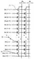
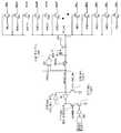
NAND 셀 열은 일반적으로 도 7에 도시된 바와 같이 직렬로 접속되는 1열 셀렉터 트랜지스터(71), i 메모리 셀(72) 및 하나의 접지 선택 트랜지스터(73)로 이루어진다. 열당 셀의 수(i)는 처리 기술에 의해 예컨대, 열당 8 셀 또는 열당 16 세 또는 열당 32 셀로 변경될 수 있다. 열당 32 메모리 셀이 현재의 90㎚ 및 70㎚ 기술에서 일반적이다. 이하, '32'가 도 7에 도시된 바와 같이 i에 대해 사용된다.The NAND cell column is generally composed of a one-
메모리 셀 게이트는 워드라인 0 내지 31(W/L 0 내지 W/L 31)에 대응한다. 열 선택 트랜지스터의 게이트는 열 선택 라인(SSL)에 접속되는 한편, 열 선택 트랜지스터의 드레인은 비트라인(B/L)에 접속된다. 접지 선택 트랜지스터의 게이트는 접지 선택 라인(GSL)에 접속되는 한편, 접지 선택 트랜지스터의 소스는 공통 소스 라인(CSL)에 접속된다. 각 워드라인은 페이지에 대응하고, 각 열은 블록에 대응한다.The memory cell gates correspond to
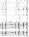
도 8 및 도 9는 NAND 셀 열당 32 셀을 갖는 블록의 물리적인 구성을 도시한다. 도 8에 도시된 바와 같이, 한 블록 내에는 (j+k)*8 NAND 열이 존재한다. 따라서, 단위 블록은 총 (j+k)*8*32 셀을 갖는다. 각 워드라인은 단위 페이지로서 정의된다. 도 9는 n 블록을 도시한다.Figures 8 and 9 illustrate the physical configuration of a block with 32 cells per NAND cell column. As shown in Fig. 8, there is a (j + k) * 8 NAND column in one block. Therefore, the unit block has a total of (j + k) * 8 * 32 cells. Each word line is defined as a unit page. Figure 9 shows n blocks.
일반적으로, 플래시 메모리 셀은 파울러-노다임(F-N: Fowler-Nordheim) 터널링 또는 열 전자 주입 중 어느 하나에 의해 프로그래밍 및 소거된다. NAND 플래시 메모리에서, 소거 및 프로그램의 양자는 F-N 터널링에 의해 관리된다. 아래의 소거 및 프로그램 동작은 NAND 플래시 메모리에 의거한다.Generally, flash memory cells are programmed and erased by either Fowler-Nordheim (F-N) tunneling or thermal electron injection. In the NAND flash memory, both the erase and the program are managed by F-N tunneling. The following erase and program operations are based on the NAND flash memory.
소거 동작 중에, 셀의 상부 폴리(top poly)(즉, 상부 게이트)는 Vss(접지)로 바이어스되는 한편, 셀의 기판은 소거 전압 Vers(예컨대, 대략 20v, 소스 및 드레인은 P-기판으로부터 n+ 소스/드레인으로의 접합-순방향-바이어스로 인해 자동으로 Vers로 바이어스된다)로 바이어스된다. 이 소거 바이어스 조건에 의해, 부동 폴리(floating poly)(즉, 부동 게이트)에 트랩된 전자(전하)가 도 10A에 도시된 바와 같이 터널 산화물을 통해 기판으로 방출된다. 소거된 셀의 셀 Vth는 도 10B에 도시된 바와 같이 음의 값이다. 바꿔 말하면, 소거된 셀은 (통상적으로 0V의 게이트 바이어스에 의해 턴-온하는) 온-트랜지스터이다.During the erase operation, the cell's top poly (i.e., top gate) is biased at Vss (ground) while the cell's substrate is erased at the erase voltage Vers (e.g., Biased to Vers automatically due to forward-biasing junction-to-source / drain coupling). With this erase bias condition, the electrons trapped in the floating poly (i.e., floating gate) are discharged to the substrate through the tunnel oxide as shown in Fig. 10A. The cell Vth of the erased cell is a negative value as shown in FIG. 10B. In other words, the erased cell is an on-transistor (which is typically turned on by a gate bias of 0V).
반대로, 프로그램 동작 중에, 셀의 상부 폴리(top poly)(즉, 상부 게이트)는 프로그램 전압 Vpgm(예컨대, 대략 18V)로 바이어스되는 한편, 셀의 기판, 소스 및 드레인은 Vss(접지)로 바이어스된다. 이 프로그램 바이어스 조건에 의해, 기판 내의 전자(전하)가 도 11A에 도시된 바와 같이 터널 산화물을 통해 기판으로 주입된다. 프로그램된 셀의 셀 Vth는 도 11B에 도시된 바와 같이 양의 값이다. 바꿔 말하면, 프로그램된 셀은 (통상적으로 0V의 게이트 바이어스에 의해 턴-오프하는) 오프-트랜지스터이다.Conversely, during a programming operation, the top poly (i.e., top gate) of the cell is biased to the program voltage Vpgm (e.g., about 18V) while the substrate, source, and drain of the cell are biased to Vss . With this program bias condition, electrons (charges) in the substrate are injected into the substrate through the tunnel oxide as shown in Fig. 11A. The cell Vth of the programmed cell is a positive value as shown in FIG. 11B. In other words, the programmed cell is an off-transistor (which is typically turned off by a gate bias of 0V).
따라서, NAND 플래시는 양방향(즉, 대칭형) F-N 터널링 메커니즘에 의해 소거 및 프로그램된다.Thus, the NAND flash is erased and programmed by a bidirectional (i.e., symmetric) F-N tunneling mechanism.
하나의 공지된 소거 스킴(scheme)은 도 12 및 도 13에 도시된다. 도 12는 소거 동작 중의 바이어스 조건을 도시한다. p-웰 기판이 소거 전압 Vers로 바이어스되는 한편, 선택된 블록 내의 비트라인 및 공통 소스 라인(CSL)은 SSL 및 GSL 트 랜지스터의 S/D 다이오드를 통해 Vers-0.6v에 클램프(clamped)된다. 동시에, 선택된 블록 내의 모든 워드라인은 0V로 바이어스되는 한편, 열 선택 라인(SSL) 및 접지 선택 라인(GSL)은 소거 전압 Vers로 바이어스된다. 따라서, 선택된 블록 내의 전체 셀이 상술한 바와 같은 F-N 터널링에 의해 소거된다.One known erase scheme is shown in FIGS. 12 and 13. FIG. 12 shows the bias condition during the erase operation. While the p-well substrate is biased with the erase voltage Vers, the bit line and common source line (CSL) in the selected block are clamped to Vers-0.6v through the S / D diode of the SSL and GSL transistors. At the same time, all the word lines in the selected block are biased at 0V, while the column select line SSL and the ground select line GSL are biased with the erase voltage Vers. Therefore, all cells in the selected block are erased by F-N tunneling as described above.
블록 베이스의 소거 동작으로 인해, 동일한 p-웰 기판을 갖는 선택되지 않은 블록 내의 메모리 셀의 소거가 방지되어야 한다(즉, 소거 금지). 도 13은 선택되지 않은 블록에 대한 소거 금지 스킴을 도시한다:Due to the erase operation of the block base, erasing of the memory cells in the unselected block having the same p-well substrate should be prevented (i.e., erasing prohibited). Figure 13 shows the erase-prevention scheme for unselected blocks:
· 선택된 블록 내의 모든 워드라인이 0V로 바이어스된다., All word lines in the selected block are biased to 0V.
· 선택되지 않은 블록 내의 모든 워드라인이 기판으로부터의 Vers에 의해 전계를 보상하기 위해 Vers로 바이어스된다., All word lines in the non-selected block are biased to Vers to compensate for the electric field by Vers from the substrate.
표 1은 소거 동작 중에 종래 기술 1에 의해 선택된 블록과 선택되지 않은 블록에 대한 바이어스 조건을 도시한다.Table 1 shows the bias condition for the block selected by the
표 1. 소거 중의 바이어스 조건 - 종래 기술 1Table 1. Bias condition during erase -

이 소거 금지 스킴을 이용하면, 선택되지 않은 블록 내의 모든 워드라인을 소거 전압 Vers로 충전하는 데 매우 긴 총 소거 시간을 필요로 한다. 동시에, 선택되지 않은 블록 내의 전체 워드라인을 충전 및 방전하기 때문에, 전력 소비가 매우 높다. 또한, 메모리 밀도가 증가함에 따라, 소거 시간이 매우 길어지고, 소거 동작 중의 전력 소비가 매우 높아진다.Using this erase inhibition scheme requires a very long total erase time to charge all the word lines in the unselected block with the erase voltage Vers. At the same time, since the entire word line in the unselected block is charged and discharged, the power consumption is very high. Also, as the memory density increases, the erase time becomes very long, and the power consumption during erase operation becomes very high.
상기 방법에서의 문제점을 해결하기 위해, 셀프-부스팅(self-boosting) 소거 금지 스킴(미국 특허 #5,473,563호)이 제안되어 있고 NAND 플래시 메모리에 널리 사용되고 있다.In order to solve the problem in the above method, a self-boosting erase prevention scheme (U.S. Patent No. 5,473,563) has been proposed and widely used in NAND flash memories.
선택된 블록에 대해서, 소거 바이어스 조건은 SSL 및 GSL이 도 14에 도시된 바와 같이, Vers로 바이어스되는 대신에 부동으로 되는 것을 제외하고, 상기와 실 질적으로 동일하다.For the selected block, the erase bias condition is practically the same as above, except that SSL and GSL are floating instead of being biased by Vers, as shown in FIG.
선택되지 않은 블록 내의 메모리 셀의 소거를 방지하기 위해, 선택되지 않은 블록 내의 모든 워드라인이 도 15에 도시된 바와 같이 소거 동작 중에 부동한다. 따라서, 선택되지 않은 블록 내의 부동하는 워드라인은 소거 전압 Vers를 기판에 인가할 때 선택되지 않은 블록 내의 기판과 워드라인 사이의 용량성 결합에 의해 거의 소거 전압 Vers로 부스트된다. (부동하는 워드라인은 셀 어레이의 기판이 Vers로 될 때 Vers의 약 90%로 부스트되지만, 부동하는 워드라인 상의 부스트된 전압 레벨은 기판과 워드라인 사이의 결합비에 의해 결정된다.) 선택되지 않은 블록 내의 워드라인 상의 부스트된 전압은 기판과 워드라인 사이의 전계를 감소시키며, 그 결과, 선택되지 않은 블록 내의 메모리 셀의 소거가 방지된다.To prevent erasure of memory cells in unselected blocks, all word lines in the unselected block float during the erase operation as shown in FIG. Thus, a floating word line in an unselected block is boosted to an almost erase voltage Vers by a capacitive coupling between the substrate and the word line in the unselected block when applying the erase voltage Vers to the substrate. (The floating word line is boosted to about 90% of Vers when the substrate of the cell array is Vers, but the boosted voltage level on the floating word line is determined by the coupling ratio between the substrate and the word line) The boosted voltage on the word line in the non-block reduces the electric field between the substrate and the word line, thereby preventing erasure of the memory cells in the non-selected block.
· 선택된 블록 내의 모든 워드라인이 0V로 바이어스된다., All word lines in the selected block are biased to 0V.
· 선택되지 않은 블록 내의 모든 워드라인이 부동으로 된다., All word lines in unselected block are in floating.
표 2는 이 방법에 의한 소거 중의 바이어스 조건을 도시한다. 선택되지 않은 블록 내의 전체 워드라인이 Vers로 바이어스될 필요가 없기 때문에, 선택되지 않은 블록 내의 워드라인에 소거 전압 Vers를 인가할 필요가 없어, 소거 중에 전력 소비를 감소시키고 소거 시간을 감소시킨다.Table 2 shows bias conditions during erasing by this method. Since the entire word line in the unselected block need not be biased with Vers, there is no need to apply the erase voltage Vers to the word line in the unselected block, thereby reducing power consumption and erasing time during erase.
표 2. 소거 중의 바이어스 조건 - 종래 기술 2Table 2. Bias condition during erasure - Prior Art 2


셀의 기판이 소건 전압 Vers로 바이어스되고 선택된 블록 내의 셀의 소스/드레인/기판이 전기적으로 접속되기 때문에, 소거 동작은 블록 베이스로 발생해야 한다. 바꿔 말하면, 최소 소거 가능한 어레이 크기가 블록이다.Since the substrate of the cell is biased with a glow voltage Vers and the source / drain / substrate of the cell in the selected block is electrically connected, the erase operation must occur on a block basis. In other words, the minimum erasable array size is a block.
상술한 플래시 메모리에는 세 가지 제한이 가해진다. 먼저, 비트는 목표 메모리 어레이를 소거한 후에만 프로그램될 수 있다. 둘째로, 각 셀은 제한된 수의 소거를 유지할 수만 있고, 그 후에 데이터를 더 이상 신뢰할 수 있게 저장할 수 없다. 바꿔 말하면, 셀에 대한 소거 및 프로그램 사이클의 수에 제한이 있다(즉, 내구성, 일반적으로 10,000∼100,000 사이클). 셋째로, 최소 소거 가능한 어레이 크기는 최소 프로그램 가능한 어레이 크기보다 매우 더 크다. 이들 제한으로 인해, 복잡한 데이터 구조 및 알고리즘이 플래시 메모리를 효율적으로 사용하는 데 필요 하다. (예컨대, 미국 특허 5,937,425호, 6,732,221호 및 6,594,183호를 참조하라.)The above-described flash memory has three restrictions. First, the bit can only be programmed after erasing the target memory array. Second, each cell can only maintain a limited number of erasures, and then can no longer reliably store the data. In other words, there is a limit on the number of erase and program cycles for the cell (i.e., durability, typically 10,000 to 100,000 cycles). Third, the minimum erasable array size is much larger than the minimum programmable array size. Due to these limitations, complex data structures and algorithms are required to efficiently use flash memory. (See, for example, U.S. Patent Nos. 5,937,425, 6,732,221 and 6,594,183)
페이지 베이스의 메모리 셀의 소거는 미국 특허 5,995,417호 및 특허 출원 US 2006/0050594호에 제안되어 있다.Erasing of page-based memory cells is proposed in U.S. Patent No. 5,995,417 and U.S. Patent Application No. 2006/0050594.
여기에는 특별한 애플리케이션 NAND 플래시 메모리를 갖는 비휘발성 메모리에서 새로운 페이지 베이스의 소거 방법의 기술적인 상세사항이 여기에 제공된다. 페이지 베이스의 소거 방법은 NAND 플래시 메모리를 사용하여 설명되지만, 당업자에 의해서 다른 플래시 메모리 장치에 더욱 일반적으로 적용될 수도 있다.Here, technical details of a method of erasing a new page base in a nonvolatile memory having a special application NAND flash memory are provided here. The page-based erase method is described using a NAND flash memory, but may be more generally applied to other flash memory devices by those skilled in the art.
NAND 플래시 메모리와 같은 비휘발성 메모리 어레이는 기판 상의 복수의 메모리 셀의 열, 메모리 셀들의 페이지들까지 상기 열들을 가로지르는 워드라인들 및 각 워드라인에 전압을 인가하는 패스 트랜지스터를 갖는다. 페이지를 소거하는 방법에서, 선택된 블록 내의 각 패스 트랜지스터는 예컨대, 블록 디코더를 통해 작동된다. 워드라인 디코더는 선택된 블록의 복수의 선택된 워드라인의 각각에서 선택 전압이 패스 트랜지스터에, 그리고 선택된 블록의 복수의 선택되지 않은 워드라인의 각각에서 비선택 전압이 패스 트랜지스터에 인가되게 할 수 있다. 기판 전압은 선택된 블록의 기판에 인가된다. 상기 기판 전압과 각 선택된 워드라인의 결과적인 전압 사이의 전압차가 상기 선택된 워드라인의 메모리 셀들의 상기 페이지를 소거시키고, 상기 기판 전압과 각 선택되지 않은 워드라인의 결과적인 전압 사이의 전압차는 상기 선택되지 않은 워드라인의 메모리 셀들의 상기 페이지를 소거하는 것 미만이다.A non-volatile memory array, such as a NAND flash memory, has columns of a plurality of memory cells on a substrate, word lines across the columns to pages of memory cells, and pass transistors that apply a voltage to each word line. In the method of erasing a page, each pass transistor in a selected block is operated, for example, through a block decoder. The word line decoder may cause a select voltage at each of the plurality of selected word lines of the selected block to be applied to the pass transistor and a non-select voltage at each of the plurality of unselected word lines of the selected block to be applied to the pass transistor. The substrate voltage is applied to the substrate of the selected block. Wherein a voltage difference between the substrate voltage and a resultant voltage of each selected word line erases the page of memory cells of the selected word line and a voltage difference between the substrate voltage and a resultant voltage of each non- Lt; RTI ID = 0.0 > of the memory cells of the word line that are not < / RTI >
특정 실시예에서, 공통 선택 전압이 각 선택된 워드라인에 인가되고, 공통 비선택 전압이 각 선택되지 않은 워드라인에 인가된다. 선택 전압 및 비선택 전압이 선택된 블록의 워드라인들 중 어느 하나에 인가될 수 있다.In a particular embodiment, a common select voltage is applied to each selected word line, and a common unselect voltage is applied to each unselected word line. A select voltage and a non-select voltage may be applied to any one of the word lines of the selected block.
선택된 블록의 워드라인들 중 어느 하나에 선택 및 비선택 전압의 인가에 의해, 선택된 워드라인이 적어도 하나의 선택되지 않은 워드라인에 의해 분리될 수 있고, 선택되지 않은 워드라인이 적어도 하나의 선택된 워드라인에 의해 분리될 수 있다. 워드라인의 부스팅이 의존하는, 선택되지 않은 라인들에 인접한 선택된 라인들에 의해, 그 부스팅을 초래하는 용량성 결합이 감소될 수 있다. 그 결과, 비선택 전압으로부터 인가되는 더 높은 초기 전압이 바람직하다. 2개의 선택된 메모리 셀에 인접한 선택되지 않은 메모리 셀이 소거되지 않는 것을 보증하기 위해, 비선택 전압이 선택 전압에 보다는 인가된 기판 전압에 더 가까운 것이 바람직하다.Selected word lines may be separated by at least one unselected word line by application of select and unselect voltage to any one of the word lines of the selected block and unselected word lines may be separated by at least one selected word Line. ≪ / RTI > By selected lines adjacent to unselected lines, to which the boosting of the word line depends, the capacitive coupling resulting in that boosting can be reduced. As a result, a higher initial voltage applied from a non-selected voltage is desirable. In order to ensure that unselected memory cells adjacent to two selected memory cells are not erased, it is desirable that the unselected voltage is closer to the applied substrate voltage than to the selected voltage.
일 실시예에서, 각 선택된 워드라인의 상기 결과적인 전압은 상기 선택 전압과 실질적으로 동일하고, 각 선택되지 않은 워드라인의 상기 결과적인 전압은 상기 비선택 전압으로부터 상기 기판 전압을 향해 결합되는 부동 전압이다. 선택된 블록의 각 패스 트랜지스터에 인가되는 공통 게이트 신호는 값 V2를 갖고, 상기 비선택 전압은 V2 보다 크며, 상기 선택되지 않은 워드라인은 V2-Vtn으로 프리차지(precharge)된다. V2는 실질적으로 상기 인가된 기판 전압 미만이지만, 바람직하게는, 상기 인가된 기판 전압의 적어도 50%이다. 그 자체로, 선택된 블록 내의 비선택 전압이 선택되지 않은 블록 내의 패스 트랜지스터에 일반적으로 인가되는 전압보다 더 크다.In one embodiment, the resulting voltage of each selected word line is substantially equal to the selected voltage, and the resulting voltage of each unselected word line is greater than the floating voltage < RTI ID = 0.0 > to be. The common gate signal applied to each pass transistor of the selected block has a value V2, the unselect voltage is greater than V2, and the unselected word line is precharged to V2-Vtn. V2 is substantially less than the applied substrate voltage, but preferably is at least 50% of the applied substrate voltage. As such, the unselected voltage in the selected block is greater than the voltage normally applied to the pass transistor in the unselected block.
다른 실시예에서는, 각 선택된 워드라인의 상기 결과적인 전압은 상기 선택 전압과 실질적으로 동일하고, 각 선택되지 않은 워드라인의 상기 결과적인 전압은 상기 비선택 전압과 실질적으로 동일하다. 예를 들어, 선택 전압은 약 0V일 수 있고, 비선택 전압은 인가된 기판 전압과 대략 동일할 수 있다.In another embodiment, the resulting voltage of each selected word line is substantially equal to the selected voltage, and the resulting voltage of each unselected word line is substantially equal to the unselected voltage. For example, the select voltage may be approximately 0V, and the unselected voltage may be approximately equal to the applied substrate voltage.
소거 검증 동작에서, 선택 검증 전압이 선택된 블록 내의 복수의 소거된 페이지의 각 워드라인에 인가될 수 있고, 비선택 검증 전압이 선택된 블록 내의 복수의 소거되지 않은 페이지의 각 워드라인에 인가될 수 있다. 각 열은 종단 전압, 특히 소스 전압에 접속된다. 종단 전압의 레벨은 선택된 워드 라인들의 수에 의존하는 복수의 전압 레벨 중 하나에서 선택될 수 있다.In an erase verify operation, a select verify voltage may be applied to each word line of a plurality of erased pages in a selected block, and a non-select verify voltage may be applied to each word line of a plurality of erased pages in the selected block . Each column is connected to a termination voltage, in particular a source voltage. The level of the termination voltage may be selected from one of a plurality of voltage levels depending on the number of selected word lines.
이상은, 다른 도면들에 걸쳐 같은 참조 문자가 동일한 부분을 나타내는 첨부한 도면에 도시된 바와 같이, 본 발명의 예시적인 실시예의 아래의 더욱 특별한 설명으로부터 명백해진다. 도면은 본 발명의 실시예들을 예시할 때 배치하는 대신에 반드시 확대, 강조할 필요는 없다.The foregoing is apparent from the following more particular description of exemplary embodiments of the invention, as illustrated in the accompanying drawings, wherein like reference characters refer to the same parts throughout the different views. The drawings are not necessarily enlarged and emphasized instead of being arranged when the embodiments of the present invention are illustrated.
도 1은 NAND 플래시 셀 어레이 구성을 도시하는 도면이다.1 is a diagram showing a NAND flash cell array configuration.
도 2는 NAND 플래시 블록 구성을 도시하는 도면이다.2 is a diagram showing a configuration of a NAND flash block.
도 3은 NAND 플래시 페이지 구성을 도시하는 도면이다.3 is a diagram showing a NAND flash page configuration.
도 4는 NAND 플래시에서의 페이지 베이스의 판독 동작을 도시하는 도면이다.4 is a diagram showing a page-based read operation in the NAND flash.
도 5는 NAND 플래시에서의 페이지 베이스의 프로그램 동작을 도시하는 도면 이다.5 is a diagram showing a page-based program operation in the NAND flash.
도 6은 NAND 플래시에서의 페이지 베이스의 소거 동작을 도시하는 도면이다.6 is a diagram showing an erasing operation of the page base in the NAND flash.
도 7은 32개의 셀을 갖는 NAND 셀 열을 도시하는 도면이다.7 is a diagram showing a NAND cell column having 32 cells.
도 8은 NAND 플래시에서의 블록 및 페이지 정의를 도시하는 도면이다.8 is a diagram showing block and page definitions in NAND Flash.
도 9는 NAND 플래시에서의 다수의 블록을 도시하는 도면이다.9 is a diagram showing a plurality of blocks in the NAND flash.
도 10A는 파울러-노다임(F-N) 터널링에 의한 소거 동작을 도시하는 도면이다.10A is a diagram showing an erase operation by Fowler-Nordheim (F-N) tunneling.
도 10B는 파울러-노다임(F-N) 터널링에 의한 소거 동작을 도시하는 도면이다.10B is a view showing an erase operation by Fowler-Nordheim (F-N) tunneling.
도 11A는 파울러-노다임(F-N) 터널링에 의한 프로그램 동작을 도시하는 도면이다.11A is a diagram showing a program operation by Fowler-Nordheim (F-N) tunneling.
도 11B는 파울러-노다임(F-N) 터널링에 의한 프로그램 동작을 도시하는 도면이다.11B is a diagram showing a program operation by Fowler-Nordheim (F-N) tunneling.
도 12는 소거 중에 선택된 블록에 대한 바이어스 조건 - 종래 기술 1을 도시하는 도면이다.12 is a diagram showing the bias condition for the selected block during erase-
도 13은 블록 소거 및 정적 소거 금지 스킴 - 종래 기술 1을 도시하는 도면이다.Figure 13 is a block diagram illustrating a block erase and static erase prevention scheme.
도 14는 소거 중에 선택된 블록에 대한 바이어스 조건 - 종래 기술 2를 도시하는 도면이다.Fig. 14 is a diagram showing a bias condition for a block selected during erasure-Prior Art 2. Fig.
도 15는 블록 소거 및 셀프-부스팅 소거 금지 스킴 - 종래 기술 2를 도시하 는 도면이다.15 is a block diagram illustrating a block erase and self-boosting erase prevention scheme, prior art 2;
도 16은 페이지 또는 페이지의 일부를 변경하기 위한 블록 복사 프로세스를 도시하는 도면이다.16 is a diagram showing a block copying process for changing a page or a part of a page.
도 17은 소거 중에 선택된 블록에 대한 바이어스 조건 - 페이지 소거 스킴 1을 도시하는 도면이다.17 is a diagram showing a bias condition-page erase
도 18은 페이지 소거 및 소거 금지 - 페이지 소거 스킴 1을 도시하는 도면이다.18 is a diagram showing a page erase and erase prohibition-page erase
도 19는 페이지 소거 바이어스 조건 - 페이지 소거 스킴 2A를 도시하는 도면이다.19 is a diagram showing a page erase bias condition-page erase scheme 2A.
도 20은 페이지 소거 및 소거 금지 - 페이지 소거 스킴 2A를 도시하는 도면이다.20 is a diagram showing a page erase and erase prohibition-page erase scheme 2A.
도 21은 페이지 소거 바이어스 조건 - 페이지 소거 스킴 2B를 도시하는 도면이다.21 is a diagram showing a page erase bias condition-page erase scheme 2B.
도 22는 페이지 소거 및 소거 금지 - 페이지 소거 스킴 2B를 도시하는 도면이다.22 is a diagram showing a page erase and erase prohibition-page erase scheme 2B.
도 23은 다수의 페이지 소거 - 페이지 소거 스킴 1을 도시하는 도면이다.FIG. 23 is a diagram showing a plurality of page erase-page erase
도 24는 다수의 페이지 소거 - 페이지 소거 스킴 2A를 도시하는 도면이다.FIG. 24 is a diagram showing a plurality of page erase-page erase schemes 2A.
도 25는 다수의 페이지 소거 - 페이지 소거 스킴 2B를 도시하는 도면이다.FIG. 25 is a diagram showing a plurality of page erase-page erase schemes 2B.
도 26은 블록 소거 - 페이지 소거 스킴 2A를 도시하는 도면이다.26 is a diagram showing a block erase-page erase scheme 2A.
도 27은 블록 소거 - 페이지 소거 스킴 2B를 도시하는 도면이다.27 is a diagram showing a block erase-page erase scheme 2B.
도 28은 소스 바이어스 없는 페이지 소거 검증을 도시하는 도면이다.FIG. 28 is a diagram showing page erase verification without source bias. FIG.
도 29는 소스 바이어스 있는 페이지 소거 검증을 도시하는 도면이다.29 is a diagram showing a page-erase verify with a source bias.
도 30은 블록 소거 검증을 도시하는 도면이다.30 is a diagram showing block erase verification.
도 31은 페이지 소거 흐름 - 단일 소거 및 소거 검증 사이클을 도시하는 도면이다.31 is a diagram illustrating a page erase flow-single erase and erase verify cycle.
도 32는 페이지 소거 흐름 - 다수의 소거 및 소거 검증 사이클을 도시하는 도면이다.32 is a diagram illustrating a page erase flow-multiple erase and erase verify cycles.
도 33은 NAND 플래시 코어의 간략화된 블록도이다.33 is a simplified block diagram of a NAND flash core.
도 34는 페이지 소거 스킴 1의 블록 디코더 개략도이다.34 is a block decoder schematic diagram of a page erase
도 35는 페이지 소거 스킴 2A 및 2B의 블록 디코더 개략도이다.35 is a block decoder schematic diagram of page erase schemes 2A and 2B.
도 36은 페이지 버퍼 및 칼럼 셀렉터 - 예를 도시하는 도면이다.Fig. 36 is a diagram showing an example of a page buffer and a column selector.
도 37은 페이지 소거/다수의 페이지 소거 타이밍 - 페이지 소거 스킴 1을 도시하는 도면이다.37 is a diagram showing a page erase / multiple page erase timing-page erase
도 38은 페이지 소거/다수의 페이지 소거 타이밍 - 페이지 소거 스킴 2A를 도시하는 도면이다.38 is a diagram showing a page erase / multiple page erase timing-page erase scheme 2A.
도 39는 페이지 소거/다수의 페이지 소거 타이밍 - 페이지 소거 스킴 2B를 도시하는 도면이다.39 is a diagram showing a page erase / multiple page erase timing-page erase scheme 2B.
도 40은 블록 소거 타이밍 - 페이지 소거 스킴 2A를 도시하는 도면이다.40 is a diagram showing a block erase timing-page erase scheme 2A.
도 41은 블록 소거 타이밍 - 페이지 소거 스킴 2B를 도시하는 도면이다.41 is a diagram showing a block erase timing-page erase scheme 2B.
도 42는 소스 바이어스를 갖는 페이지 소거 스킴 1에 대한 페이지 소거 검증 타이밍을 도시하는 도면이다.42 is a diagram showing a page erase verify timing for the page erase
도 43은 페이지 소거 스킴 1에 대한 블록 소거 검증 타이밍을 도시하는 도면이다.43 is a diagram showing the timing of block erase verification for the page erase
도 44는 페이지 소거 스킴 2A 및 2B에 대한 페이지 소거 검증 타이밍을 도시하는 도면이다.44 is a diagram showing the page erase verification timing for the page erase schemes 2A and 2B.
도 45는 페이지 소거 스킴 2A 및 2B에 대한 블록 소거 검증 타이밍을 도시하는 도면이다.45 is a diagram showing the timing of block erase verification for page erase schemes 2A and 2B.
도 46은 소거 중에 선택된 블록에 대한 바이어스 조건 - 페이지 소거 스킴 3을 도시하는 도면이다.46 is a diagram showing a bias condition-page erase scheme 3 for a block selected during erase.
도 47은 소거 중에 선택된 블록에 대한 바이어스 조건 - 페이지 소거 스킴 3을 도시하는 도면이다.47 is a diagram showing a bias condition-page erase scheme 3 for a block selected during erase.
도 48은 페이지 소거 및 소거 금지 - 페이지 소거 스킴 3을 도시하는 도면이다.FIG. 48 is a diagram showing a page erase and erase prohibition-page erase scheme 3; FIG.
도 49는 다수의 페이지 소거 및 소거 금지 - 페이지 소거 스킴 3을 도시하는 도면이다.49 is a diagram showing a plurality of page erase and erase-page erase schemes 3;
도 50은 페이지 소거 스킴 3 중의 기생 용량을 도시하는 도면이다.50 is a diagram showing the parasitic capacitance in the page erase scheme 3;
도 51은 페이지 소거/다수의 페이지 소거 타이밍 - 페이지 소거 스킴 3을 도시하는 도면이다.51 is a diagram showing a page erase / multiple page erase timing-page erase scheme 3;
본 발명의 예시적인 실시예를 아래에 설명한다.Exemplary embodiments of the invention are described below.
여기에서 인용된 모든 특허, 공개된 출원 및 참조문헌의 개시내용은 참고로 전체적으로 통합되어 있다.The disclosures of all patents, published applications and references cited herein are incorporated by reference in their entirety.
플래시 메모리 특히, NAND 플래시 장치에서, 판독 및 프로그램 동작은 페이지 베이스로 실행되는 한편, 소거 동작은 블록 베이스로 실행된다. 일반적으로, 페이지 크기는 512 바이트, 2048 바이트 또는 4096 바이트인 한편, 블록 크기는 16 페이지, 32 페이지, 도는 64 페이지이다. 따라서, 최소 소거 가능한 블록 크기는 페이지 크기보다 적어도 16배 더 크다. 또한, 이러한 최소 크기의 소거 가능한 블록(즉, 단위 소거 블록)은 칩 크기가 증가함에 따라 더 커진다.In the flash memory, in particular in the NAND flash device, the read and program operations are performed on a page basis while the erase operations are executed on a block basis. Typically, the page size is 512 bytes, 2048 bytes, or 4096 bytes, while the block size is 16 pages, 32 pages, or 64 pages. Thus, the minimum erasable block size is at least 16 times larger than the page size. In addition, this minimum size erasable block (i.e., unit erase block) becomes larger as the chip size increases.
프로그램/판독과 소거 사이의 어레이 크기 불일치는 플래시 파일 시스템에서의 시스템 성능 저하 및 장치 신뢰도(즉, 장치 수명)의 2개의 중요한 문제점을 도입한다.Array size mismatch between program / read and erase introduces two major problems: system performance degradation in the flash file system and device reliability (i.e., device life).
하드 디스크(HDD)와 달리, 플래시 메모리 장치 내의 메모리 셀은 입력 데이터에 의해 프로그램되기 전에 소거되어야 한다. 데이터 기록 동작은 시스템 내의 CPU나 플래시 제어기가 프로그램 명령을 발행하면 즉시 실행되어야 한다. 따라서, 프로그램 전 소거는 전체 시스템 성능을 저하시킨다. 이 문제점을 극복하기 위해, 플래시 제어기는 일반적으로 미리 비어 있는 소거된 블록을 준비한다(즉, 소거-유닛 교정(reclamation)). 이 교정은 백그라운드 시에(CPU가 유휴 상태일 때) 또는 프리 스페이스(free space)의 크기가 소정의 임계값 아래로 떨어질 때 요구 시에 중 어느 하나에 발생할 수 있다.Unlike a hard disk (HDD), memory cells in a flash memory device must be erased before being programmed by the input data. The data write operation must be executed immediately when a CPU or flash controller in the system issues a program command. Thus, pre-program erasure degrades overall system performance. To overcome this problem, the flash controller typically prepares an erased erased block (i. E., Erase-unit reclamation). This calibration can occur either at the time of background (when the CPU is idle) or upon request when the size of the free space falls below a predetermined threshold.
플래시 제어기가 페이지의 작은 부분에조차 데이터 기입 또는 데이터 변경을 요구할 때, 일반적으로 변경될 페이지를 포함하는 블록은 소거-유닛 교정에 의해 교정된 프리(비어 있는) 블록 중 하나에 재기록될 것이다. 이 경우에, 원래의 블록 내에 원래의 데이터를 포함하는 유효 페이지가 도 16에 도시된 바와 같이 선택된 프리 블록에 복사되어야 한다. 변경된 페이지가 판독, 변경되어 새로운 블록에 복사된 후에, 한 페이지에 변경된 데이터와 함께 페이지의 나머지에 원래의 데이터를 갖는 새로운 블록이 플래시 제어기 내의 가상 매핑 시스템에 의해 유효 블록 어드레스에 리매핑된다. (가상 매핑 시스템은 플래시 제어기에 의해 액세스되는 논리 어드레스와 플래시 메모리 내의 물리 어드레스 사이의 어드레스 해석 시스템이다.) 원래의 블록은 현재 사용하지 않고, 소거-유닛 교정 프로세스에 의해 프리 블록으로 교정될 것이다. (플래시 메모리의 데이터 구조 및 알고리즘에 대해, 참고로 전체적으로 여기에 통합되어 있는, 2005년 6월의 Eran Gal, Sivan Toledo의 "Algorithms and Data Structures for Flash Memories," ACM Computing Surveys, Vol. 37, No. 2, pp. 138∼163을 참조하라.) 상술한 블록 복사 동작으로 인한 성능 저하를 최소화화기 위해, 일반적으로 NAND 플래시 장치는 플래시 장치와 플래시 제어기 사이의 외부 트랜잭션(transaction) 없이 페이지 복사 기능을 지원한다. 그럼에도 불구하고, 프로그램/판독 및 소거 동작 사이의 어레이 크기 불일치가 큰 시스템 오버헤드 및 복잡성을 도입한다.When the flash controller requests data writing or data modification even to a small portion of the page, the block containing the page to be changed in general will be rewritten to one of the free (empty) blocks corrected by erasure-unit calibration. In this case, the valid page including the original data in the original block must be copied to the selected free block as shown in Fig. After the changed page is read, changed and copied to the new block, a new block having the original data in the remainder of the page along with the changed data in one page is remapped to the valid block address by the virtual mapping system in the flash controller. (The virtual mapping system is the address interpretation system between the logical address accessed by the flash controller and the physical address in the flash memory.) The original block will not be currently used and will be calibrated to free block by the erase-unit calibration process. (Eran Gal, Sivan Toledo, "Algorithms and Data Structures for Flash Memories," ACM Computing Surveys, Vol. 37, No, June 2005, incorporated herein by reference in its entirety for data structures and algorithms for flash memory, In order to minimize the performance degradation due to the above-described block copy operation, a NAND flash device generally performs a page copy function without an external transaction between the flash device and the flash controller. Support. Nonetheless, array size mismatch between program / read and erase operations introduces large system overhead and complexity.
플래시 메모리 셀은 파울러-노다임 터널링이나 열 전자 주입(hot electron injection) 중 어느 하나에 의해 프로그래밍 및 소거된다. 프로그램 또는 소거 동작 동안, 부동 게이트를 둘러싸는 유전체를 통해 부동 게이트로부터 또는 부동 게 이트로 전하가 전송된다. 이러한 빈번한 전하 전송이 부동 게이트와 유전체에서 전자가 트랩되게 하여, 셀의 프로그램 및 소거 특성을 저하시킨다. 후속하는 셀들은 증가한 수의 소거-프로그램 사이클에 의한 이러한 전자 트래핑으로 인해 점진적으로 더 높은 프로그램 전압 및 소거 전압을 필요로 하며, 그 결과, 셀 상의 소거-프로그램 사이클의 수가 제한된다. 일반적으로, 소거-프로그램 사이클의 최대수(즉, 셀 내구성)는 10,000과 100,000 사이이다.The flash memory cell is programmed and erased by either Fowler-Nordheim tunneling or hot electron injection. During a program or erase operation, charge is transferred from the floating gate to the floating gate via a dielectric surrounding the floating gate. This frequent charge transfer causes electrons to trap in the floating gate and in the dielectric, thereby degrading the program and erase characteristics of the cell. Subsequent cells require gradual higher program voltages and erase voltages due to this electron trapping by an increased number of erase-program cycles, resulting in a limited number of erase-program cycles on the cell. In general, the maximum number of erase-program cycles (i.e. cell durability) is between 10,000 and 100,000.
제한된 수의 소거-프로그램 사이클(내구력)은 플래시 장치의 수명을 제한한다. 가능한 한 긴 수명을 갖는 것이 바람직하며, 이것은 플래시 장치로의 액세스의 패턴에 의존한다. 단일 셀 또는 소수의 셀들로의 반복적이고 빈번한 재기록은 고장의 징후를 빨리 초래하고, 장치의 유용한 수명을 빨리 종료시킨다.A limited number of erase-program cycles (durability) limits the lifetime of the flash device. It is desirable to have as long a lifetime as possible, which depends on the pattern of access to the flash device. Repeated frequent rewriting to a single cell or a small number of cells quickly leads to a symptom of failure and quickly terminates the useful life of the device.
또한, 다수의 플래시 장치를 갖는 플래시 메모리 시스템에서는, 플래시 메모리 시스템 내의 장치들 간에 명백히 불균일한 사용이 있으면, 하나의 장치는 수명이 다하는 반면, 나머지 장치들은 그들의 수명이 상당히 남는다. 하나의 장치가 수명이 다할 때, 전체 메모리 시스템이 교체되어야 할 수 있고, 이것은 플래시 메모리 시스템의 수명을 크게 감소시킨다.Further, in a flash memory system having a plurality of flash devices, if there is apparently uneven use among the devices in the flash memory system, one device has a short life span, while the remaining devices have a considerable life span. When one device reaches its end of life, the entire memory system may have to be replaced, which greatly reduces the lifetime of the flash memory system.
재기록이 장치의 모든 셀에 균일하게 분배될 수 있으면, 각 셀은 자신이 허용 가능한 최대수의 소거에 근접하게 경험할 것이며, 그래서 고장의 징후가 가능한 많이 지연될 것이므로, 장치의 수명을 최대화시킨다. 장치의 모든 셀 전반에 걸쳐 균일한 사용에 의해 장치 수명을 연장하기 위해, 다수의 소거 횟수 평준화(wear-leveling) 기술 및 알고리즘이 플레시 메모리 시스템에 제안되어 실현되어 왔다.If the rewrite can be uniformly distributed to all cells of the device, each cell will experience close to the maximum number of erasures that it can tolerate, so that the signs of failure will be delayed as much as possible, thus maximizing the life of the device. A number of erase-wear-leveling techniques and algorithms have been proposed and implemented in flash memory systems to extend device life by uniform use across all cells of the device.
앞 단락에서 설명한 판독/프로그램 및 소거 사이의 어레이 크기 불일치로 인한 블록 복사 동작은, 블록의 페이지 내의 영향을 받지 않는 데이터가 변경된 데이터로 새로운 블록에 재기록(복사)되어야 하기 때문에 불필요한 재기록을 도입한다. 따라서, 최소 소거 가능한 어레이 크기가 블록(즉, 블록 베이스의 소거) 대신에 페이지(즉, 페이지 베이스의 소거)이면, 재기록될 페이지만 소거될 필요가 있으므로, 장치 수명을 극적으로 연장시킬 수 있다. 또한, 블록 복사 동작의 수는 페이지 베이스의 소거에 의해 크게 감소될 것이다.The block copy operation due to array size mismatch between the read / program and erase described in the previous paragraph introduces unnecessary rewriting because the data that is not affected in the page of the block must be rewritten (copied) to the new block with the changed data. Thus, if the minimum erasable array size is a page (i.e., page-based erase) instead of a block (i.e., block-based erase), then only the page to be rewritten needs to be erased, thereby extending the device lifetime dramatically. Also, the number of block copy operations will be greatly reduced by erasing the page base.
NAND 플래시 메모리 내의 각 NAND 셀 열은, 셀 기판이 장치의 NAND 셀 열 전반체 걸쳐 공통이더라도, 독립적으로 제어될 수 있다. 소거 동작 동안 블록 내의 모든 워드라인이 일반적인 NAND 플래시 장치에서의 동일한 전압 조건으로 바이어스된다. 이것이, 최소 소거 가능한 어레이 크기가 NAND 플래시 메모리 내에서 한 블록인 이유이다.Each NAND cell column in the NAND flash memory can be independently controlled even if the cell substrate is common throughout the NAND cell column of the apparatus. During the erase operation, all word lines in the block are biased to the same voltage condition in a conventional NAND flash device. This is why the minimum eraseable array size is one block in the NAND flash memory.
페이지 베이스로 플래시 메모리 셀을 소거하기 위해, NAND 셀 열의 페이지에 대응하는 각 워드라인은 별개로 및 독립적으로 제어되어야 한다.To erase a flash memory cell by page basis, each word line corresponding to a page of a NAND cell column must be controlled separately and independently.
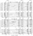
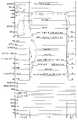
페이지 소거 스킴 1Page erase
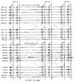
표 3 및 도 17은 페이지 소거 스킴 1에 따르는 페이지 소거 중의 바이어스 조건(예컨대, 워드라인 27의 소거)을 도시한다. 페이지 소거 스킴 1을 이용하면, 선택되지 않은 워드라인이 선택되지 않은 페이지(들)이 소거되는 것을 방지하기 위한 전압 예컨대, Vers로 바이어스되는 한편, 선택된 워드라인(들)은 선택된 페이지(들)을 소거하기 위한 다른 전압 예컨대, 0V로 바이어스된다.Table 3 and Figure 17 show bias conditions (e.g., erase of word line 27) during page erase in accordance with page erase
도 17에 도시된 바와 같이, 선택된 블록 내에서,As shown in Fig. 17, within the selected block,
· 선택된 블록 내의 선택된 워드라인(들)이 소거를 위해 0V로 바이어스되고,, The word line (s) selected in the selected block are biased to 0V to erase,
· 선택된 블록 내의 선택되지 않은 워드라인(들)은 소거 금지를 위해 Vers로 바이어스된다., (S) selected unselected word lines in the block is biased to Vers for erase prohibition.
선택되지 않은 블록 내의 메모리 셀의 소거를 방지하기 위해, 선택되지 않은 블록 내의 모든 워드라인들이 종래 기술 2와 동일하게, 소거 동작 중에 부동하는 한편, 표 3에 도시된 바이어스 조건이 도 18에 도시된 바와 같이 선택된 블록에 적용된다. 따라서, 선택되지 않은 블록 내의 부동하는 워드라인은 소거 전압(Vers)을 기판에 인가하고 있을 때 선택되지 않은 블록 내의 워드라인과 기판 사이의 용량성 결합에 의해 거의 소거 전압(Vers)으로 부스트된다. (셀 어레이의 기판이 Vers로 진행할 때 워드라인은 약 90%로 부스트되지만, 부동하는 워드라인의 부스트된 전압 레벨은 기판과 워드라인 사이의 결합비에 의해 결정된다.) 선택되지 않은 블록 내의 워드라인 상에서의 부스트된 전압은 기판과 워드라인 사이의 전계를 감소시키며, 그 결과, 선택되지 않은 블록 내의 메모리 셀의 소거가 방지된다.In order to prevent the erasure of the memory cells in the unselected block, all the word lines in the unselected block are floated during the erase operation as in the prior art 2, while the bias condition shown in Table 3 is shown in Fig. 18 As shown in FIG. Thus, a floating word line in an unselected block is boosted to an almost erase voltage Vers by a capacitive coupling between the word line and the substrate in the unselected block when applying the erase voltage Vers to the substrate. (The word line is boosted to about 90% as the substrate of the cell array advances to Vers, but the boosted voltage level of the floating word line is determined by the coupling ratio between the substrate and the word line.) The word in the non- The boosted voltage on the line reduces the electric field between the substrate and the word line, thereby preventing erasure of the memory cells in the unselected block.
· 선택되지 않은 블록 내의 모든 워드라인은 부동한다., All word lines in the unselected block floating.
표 3. 페이지 소거 중의 바이어스 조건 - 페이지 소거Table 3. Biasing conditions during page erase - page erase스킴Scheme 1 One

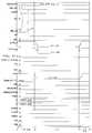
페이지 소거Page clear스킴Scheme 2A 및 2B 2A and 2B
페이지 소거 스킴 2A 및 2B에 대한 바이어스 조건은 아래와 같다:The bias conditions for the page erase schemes 2A and 2B are as follows:
· 셀 게이트(워드라인)이 음의 전압-V1(제1 레벨 전압)으로 바이어스된다.The cell gate (word line) is biased to a negative voltage -V1 (first level voltage).
· 셀 기판이 제2 레벨 전압으로 바이어스된다.The cell substrate is biased to a second level voltage.
· 셀 게이트와 기판 사이의 전계가 셀의 터널 산화물을 통해 F-N 터널링을 초래하기 위한 요건을 충족해야 한다., And the electric field between the cell gate and the substrate must meet the requirement to cause FN tunneling through the tunnel oxide of the cell.
· 셀의 부동 폴리(즉, 부동 게이트) 내에 트랩된 전자(전하)가 터널 산화물을 기판에 방출된다., It is discharged to the floating poly (that is, floating gate), an electron (electric charge) trapped in the tunnel oxide of the cell to the substrate.
· 0V의 셀 게이트 전압을 갖는 제2 레벨 전압의 최대는 선택되지 않은 이웃 하는 페이지 상에 셀 소거 방해(예컨대, 시프트하는 임계 전압 또는 소프트-소거)를 도입하지 않아야 한다.Should not be introduced into the-, the maximum voltage level of the second cell having a gate voltage of 0V is erased cell interference on the adjacent page (for example soft or erase threshold voltage shift) are not selected.
· -V1 및 제2 레벨 전압이 프로세스 기술 및 셀 특성에 따라 변화될 수 있다.· -V1 and the second voltage level may be changed depending on the process technology and cell characteristics.
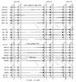
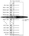
도 19는 소거 동작 중에 선택된 블록 내의 선택된 페이지(이 예에서는 워드라인 27)에 대해 페이지 소거 스킴 2A를 갖는 전압 바이어스 조건을 도시한다. 선택된 워드라인 27(페이지)은 음의 전압 -18V(-V1)인 한편, 선택되지 않은 워드라인은 0V로 바이어스된다. 셀 어레이의 기판은 0V(V2=0V)로 바이어스된다. 또한, 전압은, 도 21 및 22와 표 5와 관련하여 아래에 설명하는 프로세스 기술 및 셀 특성에 따라 변화될 수 있다. 새로운 소거 조건에 의해, 선택된 페이지 내의 모든 셀들이 소거되는 한편, 선택되지 않은 페이지의 모든 셀은 셀 게이트와 기판 사이의 전계의 효과적이지 못한 크기로 인해 소거되지 않는다.FIG. 19 shows a voltage bias condition with a page erase scheme 2A for a selected page (word line 27 in this example) in a selected block during an erase operation. The selected word line 27 (page) is negative voltage-18V (-V1) while the unselected word line is biased to 0V. The substrate of the cell array is biased to 0V (V2 = 0V). In addition, the voltage can be changed according to the process technology and the cell characteristics described below with reference to Figs. 21 and 22 and Table 5. By the new erase condition, all the cells in the selected page are erased, while all the cells of the unselected page are not erased due to the ineffective size of the electric field between the cell gate and the substrate.
표 4와 도 20은 선택되 블록과 선택되지 않은 블록에 대한 바이어스 조건을 도시한다. 선택되지 않은 블록의 모든 워드라인은 소거 중에 부동하고, 따라서 기판이 0V로 바이어스되기 때문에 모든 워드라인의 전위는 0V로 유지되며, 선택되지 않은 블록의 모든 워드라인은 소거를 위해 부동하기 전에 0V로 방전된다.Table 4 and Figure 20 show the bias conditions for the selected and unselected blocks. All the word lines of the unselected block are floated during erase and thus the potential of all word lines is held at 0V because the substrate is biased to 0V and all the word lines of the unselected block are held at 0V before floating to erase Is discharged.
표 4. 소거 중의 바이어스 조건 - 페이지 소거Table 4. Biasing conditions during erase - page erase스킴Scheme 2A 2A

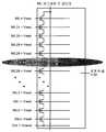
도 21은 소거동작 중에 선택된 블록 내의 선택된 페이지(이 예에서는 워드라인 27)에 대한 페이지 소거 스킴 2B를 갖는 전압 바이어스 조건을 도시한다. 선택된 워드라인 27(페이지)은 음의 전압 -13V(-V1)로 바이어스되는 한편, 선택되지 않은 워드라인은 0V로 바이어스된다. 셀 어레이의 기판은 5V로 바이어스된다. 셀의 기판과 게이트 사이의 총 전계는 제1 예의 것과 동일하다. 기판으로의 전압은 동일한 NAND 셀 열에서의 선택되지 않은 워드라인(페이지) 상의 셀에 소거 방해(즉, 소프트-소거)를 도입하지 않도록 결정되어야 한다.FIG. Shows a voltage bias condition with a page erase scheme 2B for a selected page (word line 27 in this example) in a selected block during operation. The selected word line 27 (page) is biased to negative voltage -13V (-V1) while the unselected word line is biased to 0V. The substrate of the cell array is biased at 5V. The total electric field between the substrate and the gate of the cell is the same as that in the first example. The voltage to the substrate must be determined not to introduce an erase interruption (i.e., soft-erase) to cells on unselected word lines (pages) in the same NAND cell column.
표 5 및 도 22는 선택된 블록 및 선택되지 않은 블록에 대한 바이어스 조건을 도시한다. 선택되지 않은 블록의 모든 워드라인은 소거 동작 중에는 부동하고, 선택되지 않은 블록의 모든 워드라인은 기판에 전압을 인가하고 있을 때 선택되지 않은 블록 내의 워드라인과 기판 사이의 용량성 결합에 의해 거의 기판 전압으로 부스트된다. (부스트된 전압은 기판 전압의 약 90%이지만, 부동하는 워드라인 상에서의 부스트된 전압 레벨은 워드라인과 기판 사이의 결합비에 의해 결정된다.) 선택되지 않은 블록 내의 워드라인 상의 부스트된 전압은 워드라인과 기판 사이의 전계를 감소시키며, 그 결과, 선택되지 않은 메모리 셀의 소거가 방지된다.Table 5 and Figure 22 show bias conditions for selected and unselected blocks. All the word lines of the unselected block are floating during the erase operation and all the word lines of the unselected block are capacitively coupled between the word lines and the substrate in the non- Boosted to voltage. (The boosted voltage is about 90% of the substrate voltage, but the boosted voltage level on the floating word line is determined by the coupling ratio between the word line and the substrate.) The boosted voltage on the word line in the non- Thereby reducing the electric field between the word line and the substrate, and as a result, erasing of unselected memory cells is prevented.
표 5. 소거 중의 바이어스 조건 - 페이지 소거Table 5. Biasing conditions during erase - page erase스킴Scheme 2B 2B

다수 페이지 소거 및 블록 소거Multiple page erase and block erase
새로운 페이지 소거 개념에 의해, 선택된 블록 내의 다수의 페이지(워드라인)가 소거될 수 있다. 실제로, 워드라인 전압의 선택적인 제어에 의해, 선택된 블록의 어느 하나 이상의 페이지가 소거될 수 있다. 또한, 선택된 블록의 전체 페 이지가 또한 소거될 수 있으며, 이것이 기본적으로 블록 소거이다.By the new page erase concept, a plurality of pages (word lines) in a selected block can be erased. In practice, by selective control of the word line voltage, one or more pages of the selected block may be erased. In addition, the entire page of the selected block may also be erased, which is essentially a block erase.
도 23은 페이지 소거 스킴 1의 바이어스 조건을 사용하여 동시에 소거되는 선택된 블록 내의 3개의 페이지(워드라인 1, 27, 29)를 도시한다.Figure 23 shows three pages (
도 24는 페이지 소거 스킴 2A의 바이어스 조건을 사용하여 동시에 소거되는 선택된 블록 내의 3개의 페이지(워드라인 1, 27, 29)를 도시한다.Figure 24 shows three pages (
도 25는 페이지 소거 스킴 2B의 바이어스 조건을 사용하여 동시에 소거되는 선택된 블록 내의 3개의 페이지(워드라인 1, 27, 29)를 도시한다.Figure 25 shows three pages (
도 26은 블록 소거인 페이지 소거 스킴 2A의 바이어스 조건을 사용하여 동시에 소거되는 선택된 블록 내의 모든 페이지를 도시한다.Figure 26 shows all pages in a selected block that are simultaneously erased using the bias condition of the block erase in page erase scheme 2A.
도 27은 블록 소거인 페이지 소거 스킴 2B의 바이어스 조건을 사용하여 동시에 소거되는 선택된 블록 내의 모든 페이지를 도시한다.Figure 27 shows all the pages in a selected block that are simultaneously erased using the bias condition of the block erase in page erase scheme 2B.
소거 검증Erase verification
선택된 블록 내의 단일 페이지 또는 다수의 페이지 또는 모든 페이지를 소거한 후에, 소거된 셀이 판독되기에 적절한 임계 전압 마진을 갖는 것을 보증하도록 소거 검증이 실행되어야 한다. 이 소거 검증은 아래에 설명되는 페이지 버퍼에 의해 실행된다. 도 28, 도 29, 도 30, 및 표 6은 페이지 소거 검증 및 블록 소거 검증 중의 전압 바이어스 조건을 도시한다. 다수 페이지 검증을 위해, 각 선택된 페이지는 아마도 소거 후에 연속적으로(순차적으로) 검증되지만, 바람직한 방법에서는, 모두 한번에 검증된다. 표 6에서의 전압 수들(numbers)(즉, Vread, Versvf, Vcslevf 및 Vbersvf)은 프로세스 기술 및 셀 특성에 따라 변화될 수 있다.Erase verification must be performed to ensure that after erasing a single page or multiple pages or all pages within a selected block, the erased cell has an appropriate threshold voltage margin to be read. This erase verify is performed by the page buffer described below. Figures 28, 29, 30, and Table 6 show voltage bias conditions during page erase verify and block erase verify. For multiple page verification, each selected page is probed sequentially (sequentially), perhaps after erasing, but in the preferred method, all are verified at once. The numbers of voltages in Table 6 (i.e., Vread, Versvf, Vcslevf, and Vbersvf) may vary depending on the process technology and cell characteristics.
도 28은 소스 바이어스 없는 단일 페이지 소거 검증을 도시하고, 도 29는 CSL로부터의 소스 바이어스를 갖는 단일 페이지 소거 검증을 도시한다. 도 30은 블록 소거 검증을 도시한다.Figure 28 shows a single page erase verify without source bias, and Figure 29 shows a single page erase verify with source bias from CSL. Figure 30 shows block erase verification.
표 6. 소거 검증 중의 바이어스 조건Table 6. Bias conditions during erase verification

표 6의 최종 칼럼은 모든 워드라인이 선택되는 블록 소거 검증을 도시한다. 그들 조건은 종래의 블록 소거 검증과 비교될 수 있다. 0 볼트, 또는 덜 관용적인 검증에 있어서는, -1.5V와 같은 마이너스 전압이 각 워드라인에 인가된다. 도 10B를 참조함으로써 알 수 있는 바와 같이, 적절하게 소거된 메모리 셀은 워드라인에 인가된 0 볼트로 통전할 것이다. 그러나, 메모리 셀이 완전히 소거되지 않은 경우, 메모리 셀은 덜 또는 전혀 통전하지 않는다. 블록 소거 검증 시에, 완전히 통전하는 데 실패한 메모리 셀 중 어느 하나가 완전히 소거하는 데 실패한 것으로서 감지될 수 있는 비트라인 상에 더 높은 전압을 결과로서 생성한다.The final column of Table 6 shows the block erase verification in which all word lines are selected. These conditions can be compared with conventional block erase verification. For zero volts, or less tolerant verification, a minus voltage, such as -1.5V, is applied to each word line. As can be seen by reference to FIG. 10B, a properly erased memory cell will conduct at zero volts applied to the word line. However, when the memory cell is not completely erased, the memory cell is less or no energized. At block erase verification, any one of the memory cells that failed to fully energize will result in a higher voltage on the bit line that can be sensed as having failed to erase completely.
그 페이지만이 소거된 단일 선택된 페이지에 의한 소거 검증의 경우에는, 열의 다른 메모리 셀의 각각이 온 상태나 오프 상태 중 어느 하나에 있을 수 있다. 그것을 설명하기 위해, 예컨대, 4∼5V의 고전압이 각각의 선택되지 않은 셀의 워드라인에 인가된다. 그 전압은 셀이 도 11B에 도시된 바와 같이 오프 상태로 프로그램되었을 때에도 임계 전압보다 더 높다. 따라서, 셀은 그것이 오프 상태로 프로그램된 경우에도 통전할 것이고, 모든 선택되지 않은 메모리 셀이 통전할 것이다. 선택된 워드라인을 0 볼트로 설정하면 바로 선택된 워드라인을 검증할 수 있게 된다.In the case of erase verification by a single selected page in which only that page is erased, each of the other memory cells in the column can be in either an on state or an off state. To illustrate this, a high voltage of, for example, 4-5 V is applied to the word line of each unselected cell. The voltage is also higher than the threshold voltage when the cell is programmed to the off state as shown in Figure 11B. Thus, the cell will energize even when it is programmed to the off state, and all unselected memory cells will be energized. If the selected word line is set to 0 volts, the selected word line can be directly verified.
열 내의 모든 선택되지 않은 셀의 높은 통전에 의해, 검증 동작 중에 일반적인 것보다 비트 라인 상에서 더 낮은 전압이 기대된다. 선택되지 않은 메모리 셀의 그 증가된 통전을 오프셋하기 위해, 표 6의 두 번째 칼럼에서의 -1.5V와 같은 음의 전압이 선택된 워드라인에 인가될 수 있거나, 표 6의 칼럼 1에 도시된 0.4V와 같은 0 볼트보다 더 큰 전압이 공통 소스 라인에 인가될 수 있다. 그 결과, 검증을 위해, 선택된 메모리 셀은 선택되지 않은 셀의 더 높은 컨덕턴스를 오프셋하도록 검증을 위해 더욱 도전성이어야 한다.Due to the high energization of all unselected cells in the column, a lower voltage is expected on the bit line than is common during the verify operation. To offset its increased energization of unselected memory cells, a negative voltage, such as -1.5 V in the second column of Table 6, may be applied to the selected word line, or a voltage of 0.4 A voltage greater than zero volts, such as V, may be applied to the common source line. As a result, for verification, the selected memory cell must be more conductive for verification to offset the higher conductance of the unselected cell.
일반적으로 음의 전압보다는 양의 바이어스 전압을 생성하는 것이 바람직하 므로, 양의 공통 소스 바이어스에 의한 페이지 소거 검증이 일반적으로 바람직하다. 공통 소스 라인의 적절한 전압은 예를 들면, 단일 페이지에 대해 0.3V∼0.5V의 범위로 될 수 있다. 전체 블록 미만의 다수의 페이지 소거 검증을 위해서는, 더 낮은 전압이 적절하다. 예를 들면, 전체 블록 소거 검증을 위한 0V 공통 소스 전압 및 1 페이지 검증을 위한 0.5V에 의해, 첫 번째 페이지와 동시에 검증되는 각각의 부가적인 페이지에 대해 0.5/32의 증분만큼 0.5V로부터 소스 전압을 감소시키는 것이 적절할 수 있다. 그러한 소스 전압의 미세 제어는 불필요하다. 그러나, 0.5V의 소스 전압은 예를 들면, 한번에 0 내지 8의 선택된 워드라인의 검증에 사용될 수 있고, 0.4V는 9 내지 16의 선택 워드라인의 검증에 사용될 수 있으며, 0.3V는 17∼24 워드라인용으로, 그리고 0V는 25∼32 워드라인용으로 사용될 수 있다.Since it is generally desirable to generate a positive bias voltage rather than a negative voltage, page erase verification by a positive common source bias is generally desirable. The appropriate voltage of the common source line may range, for example, from 0.3V to 0.5V for a single page. For multiple page erase verification of less than full block, lower voltages are appropriate. For example, by a 0.5 V common source voltage for full block erase verification and 0.5 V for one page verification, from 0.5 V by 0.5 / 32 increments for each additional page verified at the same time as the first page, May be appropriate. Fine control of such a source voltage is unnecessary. However, a source voltage of 0.5 V can be used, for example, to verify a selected word line from 0 to 8 at a time, 0.4 V can be used to verify a selected word line from 9 to 16, For the word line, and 0V for the 25 to 32 word line.
페이지 소거 흐름Page clear flow
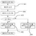
프로그램 동작과 달리, 일반적으로 소거 동작은, 단일 소거 및 소거 검증 사이클 후에 셀의 임계 전압이 목표값으로 정확하게 분배되므로, 다수의 소거 및 소거 검증 사이클을 필요로 하지 않는다. 그러나, 다수의 소거 및 소거 검증 사이클이 또한 소거된 셀의 목표 임계 전압을 보증하기 위해 적용될 수도 있다.Unlike program operation, the erase operation in general does not require multiple erase and erase verify cycles, since the cell's threshold voltage is correctly distributed to the target value after a single erase and erase verify cycle. However, multiple erase and erase verify cycles may also be applied to ensure the target threshold voltage of the erased cell.
도 31은 단일 소거 및 소거 검증 사이클을 사용하는 페이지 소거 흐름을 도시하는 한편, 도 32는 다수의 소거 및 소거 검증 사이클을 사용하는 페이지 소거 흐름을 도시한다. 다수의 소거 및 소거 검증 사이클 방법을 위한 소거 및 소거 검증 사이클의 최대수는 미리 정해지고, 프로세스 방법 및 셀 특성에 따라 변화된다. 이 페이지 소거 알고리즘(흐름)은 플래시 메모리 장치에서의 페이지 소거 명령을 발행한 후에 자동으로 실행된다.Figure 31 shows a page erase flow using a single erase and erase verify cycle, while Figure 32 shows a page erase flow using multiple erase and erase verify cycles. The maximum number of erase and erase verify cycles for multiple erase and erase verify cycle methods is predetermined and varies depending on the process method and cell characteristics. This page erase algorithm (flow) is executed automatically after issuing a page erase command in the flash memory device.
도 31의 311에서, 전체 블록을 포함하여 전체 블록까지 하나 이상의 선택된 페이지가 소거된다. 312에서, 그 하나 이상의 페이지가 소거되었는지 검증된다. 313으로부터, 메모리가 검증을 패스하면, 상태 레지스터가 314에서 패스로 업데이트되고, 그렇지 않으면, 상태 레지스터가 315에서 실패로 업데이트된다.311 of Fig. 31, one or more selected pages are erased to the entire block including the entire block. At 312, it is verified that the one or more pages have been erased. From 313, if the memory passes the validation, the status register is updated from 314 to the path, otherwise the status register is updated to 315 failed.
이와 달리, 도 32에 도시된 바와 같이, 값 ERS_loop가 320에서 1로 설정된다. 313에서 패스하지 못한 경우에, ERS_loop 값은 321에서 최대값과 비교된다. 최대값이 도달되지 못한 경우, 322에서 그 값이 증가되어, 소거 및 검증 절차가 반복된다. 루프의 최대수에 도달되었으면, 315에서 레지스터에 실패가 나타난다. Alternatively, as shown in FIG. 32, the value ERS_loop is set to 1 at 320. If the pass fails at 313, the ERS_loop value is compared to the maximum at 321. If the maximum value is not reached, its value is increased at 322 and the erase and verify procedure is repeated. If the maximum number of loops is reached, the register fails at 315.
이와 달리, 다수의 페이지 소거 후에, 각 선택된 페이지가 개별적으로 검증될 수도 있다. 개별 페이지의 순차적인 검증에 의해, 다수의 페이지 소거가 어느 한 페이지의 실패 후에 반복될 수 있거나, 실패한 페이지만 다시 소거될 수도 있다.Alternatively, after multiple page erasing, each selected page may be verified separately. By sequential verification of the individual pages, a number of page erasures may be repeated after a failure of either page, or only failed pages may be erased again.
회로 실시의 예Example of Circuit Implementation
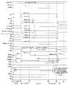
도 33은 NAND 플래시 코어의 간략화된 블록도를 도시한다. NAND 셀 어레이(331)는 종래의 NAND 플래시처럼 n개의 블록(332)을 포함한다. 페이지 버퍼 회로(333)가 판독, 프로그램 검증 및 소거 검증 중에 셀 데이터를 감지하여 래치(latch)한다. 또한, 페이지 버퍼 회로는 입력 데이터를 일시적으로 보유하고, 프로그램 동작 중에 입력 데이터에 따라 비트라인의 전압을 결정한다. NAND 셀 어레이로부터의 모든 (j+k)*8 비트라인이 페이지 버퍼 회로에 접속된다. 각 NAND 셀 블록에 대응하는 블록 디코더(334)는 신호를 SSL(열 선택 라인), 워드라인 0(WL0) 내지 31(WL31) 및 GSL(접지 선택 라인)로서 제공한다. 블록 디코더는 로우 프리디코더(335)로부터의 로우 프리디코드된 어드레스 신호 Xp/Xq/Xr/Xt와, 공통 워드라인 디코더(336)로부터의 열 선택 신호 SS, 접지 선택 신호 GS 및 공통 열 디코드 신호 S0 내지 S31에 의해 구동된다. 기판 전압이 차지 펌프(337)로부터 PP-웰에 인가된다.Figure 33 shows a simplified block diagram of a NAND flash core. The
이 문서에서는, 입력 및 출력 회로, 제어 회로, 로우 및 칼럼 프리디코더 회로, 내부 고전압 발생기에 대해, 이들이 다수의 공개된 논문 및 특허에 잘 설명되어 있으므로, 설명하지 않는다. 참고로 전체적인 내용이 통합되어 있는 참조 문헌 Kang-Deog Suh 등의 1995년 4월의 "A 3.3 V 32 Mb NAND Flash Memory with Incremental Step Pulse Programming Scheme," IEEE J Solid-State Circuits, vol. 30, no. 11, pp.1149-1156, Jin-Ki Kim 등의, 1997년 4월의 "A 120-mm 64-Mb NAND Flash Memory Achieving 180 ns/Byte Effective Program Speed," IEEE J Solid-State Circuits, vol. 32, no. 5, pp. 670-680, Ken Takeuchi 등의, 2006년 2월의 "A 56nm CMOS 99mm2 8Gb Multi-level NAND Flash Memory with 10MB/s Program Throughput," ISSCC Dig. Tech. Paper, pp. 144-145, 및 June Lee 등의, 2003년 11월의 "A 90-nm CMOS 1.8-V 2-Gb NAND Flash Memory for Mass Storage Applications," IEEE J Solid- State Circuits, vol. 38, no. 11, pp. 1934-1942를 참조하라.This document does not describe input and output circuits, control circuits, row and column predecoder circuits, and internal high voltage generators, as they are well described in a number of published articles and patents. Refer to "A 3.3 V 32 Mb NAND Flash Memory with Incremental Step Pulse Programming Scheme, IEEE J Solid-State Circuits, vol. 30, no. 11, pp.1149-1156, Jin-Ki Kim et al., "A 120-mm 64-Mb NAND Flash Memory Achieving 180 ns / Byte Effective Program Speed", IEEE J Solid-State Circuits, vol. 32, no. 5, pp. 670-680, Ken Takeuchi et al., "A 56nm CMOS 99mm2 8Gb Multi-level NAND Flash Memory with 10MB / s Program Throughput," ISSCC Dig. Tech. Paper, pp. 144-145, and June Lee, et al., "A 90-nm CMOS 1.8-V 2-Gb NAND Flash Memory for Mass Storage Applications," IEEE J Solid-State Circuits, vol. 38, no. 11, pp. See 1934-1942.
도 9의 종래의 플래시 장치에서와 같이, NAND 셀 어레이는 n개의 블록으로 이루어지고, 각 블록은 32(m)개의 소거 가능한 및 프로그램 가능한 페이지(즉, 워드라인)으로 세분할된다. NAND 셀 어레이 내에는 (j+k)*8개의 비트라인이 존재한다. 블록의 수 n, 페이지의 수 m 및(j+k)*8의 수는 변화될 수 있다는 점에 주의하라.As in the conventional flash device of Fig. 9, the NAND cell array consists of n blocks, each of which is subdivided into 32 (m) erasable and programmable pages (i.e., word lines). In the NAND cell array, (j + k) * 8 bit lines exist. Note that the number of blocks n, the number of pages m, and the number of (j + k) * 8 may vary.
도 34는 본 발명에 대해 특히, 페이지 소거 스킴 1에 대해 가능한 예 중의 하나인 블록 디코더의 회로 개략도를 도시한다. 블록 디코더에 대한 회로 실시의 다수의 변형이 존재하는 것에 주의하라. 블록 디코더의 총 수는 n이다.34 shows a circuit schematic diagram of a block decoder, which is one of the possible examples for the page erase
열 선택 라인 SSL, 워드라인 WL0 내지 WL31 및 접지 선택 라인 GSL은 블록 디코더의 출력 신호 BD_out에 의해 공통으로 제어되는 패스 트랜지스터 TSS, TS0 내지 TS31 및 TGS를 통해 SS, S0 내지 S31 및 GS의 공통 신호에 의해 구동된다.The column select line SSL, the word lines WL0 to WL31, and the ground select line GSL are connected to common signals SS, S0 to S31 and GS through pass transistors TSS, TS0 to TS31 and TGS commonly controlled by the block decoder output signal BD_out .
로컬 차지 펌프(341)는 프로그램 전압(Vpgm), 패스 전압(Vpass), 판독 전압(Vread7), 및 소거 전압(Vers)을 제공하기 위한 고전압 스위칭 회로이다. 그 펌프는 인핸스먼트(enhancement) NMOS 트랜지스터(ENH), 디플리션(depletion) NMOS 트랜지스터(DEP), 네이티브(native) NMOS 트랜지스터(NAT) 및 2-입력 NAND 게이트(G1)로 이루어진다. 블록 디코더의 출력 신호 BD_out은 블록 디코더 래치 출력BDLCH_out이 Vdd이고, HVenb가 0V이며, OSC가 발진될 때 Vhv로 상승한다(주의: 로컬 차지 램프는 잘 알려진 회로 기술이다).The
BDLCH_out은 블록 디코드 리셋 트랜지스터로의 RST_BD가 높을(실제로 단펄스) 때 0V로 리셋되고, 블록 디코드 인에이블 트랜지스터로의 LCHBD 입력이 NAND 게이트(G2)로의 Xp, Xq, Xr 및 Xt의 유효 로우 프리디코드된 어드레스 신호에 의해 높을(실제로 단펄스) 때 래치된다. BDLCH_out은 인버터(I1 및 I2)에 의해 래치된다.BDLCH_out is reset to 0V when RST_BD to the block decode reset transistor is high (actually a short pulse), and the LCHBD input to the block decode enable transistor is set to an effective low pre-decode of Xp, Xq, Xr and Xt to NAND gate G2 (Actually a short pulse) by the addressed address signal. BDLCH_out is latched by inverters I1 and I2.
도 35는 페이지 소거 스킴 2A 및 2B용의 블록 디코더의 회로 개략도를 도시한다. 블록 디코더에 대한 회로 실시의 다수의 변형이 존재하는 것에 주의하라. 블록 디코더의 총 수는 n이다.Fig. 35 shows a circuit schematic diagram of a block decoder for page erase schemes 2A and 2B. Note that there are many variations of circuit implementation for block decoders. The total number of block decoders is n.
열 선택 라인 SSL, 워드라인 WL0 내지 WL31 및 접지 선택 라인 GSL은 블록 디코더의 출력 신호 BD_out에 의해 공통으로 제어되는 패스 트랜지스터 TSS, TS0 내지 TS31 및 TGS를 통해 SS, S0 내지 S31 및 GS의 공통 신호에 의해 구동된다. 패스 트랜지스터 TSS, TS0 내지 TS31 및 TGS의 기판은 음의 고전압 Vnhv에 의해 제어된다.The column select line SSL, the word lines WL0 to WL31, and the ground select line GSL are connected to common signals SS, S0 to S31 and GS through pass transistors TSS, TS0 to TS31 and TGS commonly controlled by the block decoder output signal BD_out . The substrates of the pass transistors TSS, TS0 to TS31 and TGS are controlled by the negative high voltage Vnhv.
고전압 레벨 시프터(351)는 양의 고전압 Vhv 및 음의 고전압 Vnhv를 제공하기 위한 고전압 스위칭 회로이다. 레벨 시프터 회로는 교차 결합되는 p-채널 트랜지스터(Q1 및 Q2)와 n-채널 풀 다운 장치(Q3 및 Q4)를 포함한다. Q3으로의 입력 및 I3이 높을 때, BD_out은 Vhv가 Q1을 통해 인가되고 있을 때 높아지고, 낮아질 때 Bd_out은 Q4를 통해 Vnhv로 낮아진다.The high voltage level shifter 351 is a high voltage switching circuit for providing a positive high voltage Vhv and a negative high voltage Vnhv. The level shifter circuit includes p-channel transistors Q1 and Q2 cross-coupled and n-channel pull-down devices Q3 and Q4. When the input to Q3 and I3 are high, BD_out goes high when Vhv is being applied through Q1, and Bd_out goes low through V4 to Vnhv when low.
BD_out은 RST_BD가 높을(실제로 단펄스) 때 0V로 리셋되고, LCHBD가 게이트(G2)로의 Xp, Xq, Xr 및 Xt의 유효 로우 프리디코드된 어드레스 신호에 의해 높을(실제로 단펄스) 때 인버터(I1 및 I2)에 의해 래치된다.BD_out is reset to 0V when RST_BD is high (actually a short pulse), and when LCHBD is high (actually a short pulse) by an effective low pre-decoded address signal of Xp, Xq, Xr and Xt to gate G2, And I2.
표 7은 다양한 동작 모드에 대한 Vhv 및 Vnhv의 일례를 도시한다. 모든 전압 수들은 변경될 수 있다.Table 7 shows an example of Vhv and Vnhv for various operating modes. All voltage numbers can be changed.
표 7.Table 7.VhvVhv 및 AndVnhvVnhv 조건 - 페이지 소거 Condition - page clear스킴Scheme 2A 및 2B 2A and 2B

페이지 버퍼 및 칼럼 셀렉터 회로는 도 36에 도시된 바와 같이, 종래의 NAND 플래시에서와 동일하다. 또한 도 36에 도시된 페이지 버퍼 및 칼럼 셀렉터 회로는 이 발명에 대한 가능한 예들 중 하나이다.The page buffer and column selector circuits are the same as in the conventional NAND flash, as shown in Fig. Also, the page buffer and column selector circuit shown in Fig. 36 is one of possible examples of the present invention.
하나의 페이지 버퍼는 하나의 비트라인에 대응한다. 그러나, 페이지 버퍼는 어레이 밀도가 증가할 때 다수의 비트라인에 의해 공유될 수 있다(그 전체 내용이 참고로 통합되어 있는 참조문헌 June Lee 등의, 2003년 11월의 "A 90-nm CMOS 1.8-V 2-Gb NAND Flash Memory for Mass Storage Applications," IEEE J Solid- State Circuits, vol. 38, no. 11, pp. 1934-1942를 참조하라.)One page buffer corresponds to one bit line. However, the page buffer can be shared by multiple bit lines when the array density is increased (see A < RTI ID = 0.0 > 90-nm CMOS 1.8 < / RTI > -V 2-Gb NAND Flash Memory for Mass Storage Applications, "IEEE J Solid-State Circuits, vol.38, No. 11, pp. 1934-1942.)
도 36의 페이지 버퍼 및 칼럼 셀렉터 회로는 판독, 프로그램 검증 및 소거 검증 동작에 사용된다. 소거 검증 동작에서, 래치는 노드 B를 높게 래치하도록 LCHDA에 의해 리셋된다. 비트라인 BL은 Vcc로 프리차지된다. 모든 선택된 메모리 셀이 적절히 소거되면, 메모리 셀의 열은 소거 검증 동작 중에 통전할 것이므로, 비트라인 및 노드 PBSO를 낮게 한다. 비트라인 분리 트랜지스터는 오프로 유지한다. 약 0.5v 미만의 PBSO에 의해, 래치 아래의 감지 트랜지스터가 턴 온하지 않 아, 노드 B가 높은 상태로 유지된다. B 노드 상의 고전압은 패스/실패 p-채널 감지 트랜지스터를 오프로 유지한다. 그 결과, 그 감지 트랜지스터는 초기에 접지된 라인 PASSb를 충전하지 않는다. 모든 열이 적절히 소거되면, 라인 PASSb가 낮은 상태로 유지되고, "패스"가 그 라인으로부터 감지된다.The page buffer and column selector circuit of Figure 36 is used for read, program verify and erase verify operations. In the erase verify operation, the latch is reset by LCHDA to latch the node B high. The bit line BL is precharged to Vcc. If all selected memory cells are properly erased, the column of memory cells will energize during the erase verify operation, thus lowering the bit line and node PBSO. The bit line isolation transistor is kept off. With less than about 0.5 V of PBSO, the sense transistor under the latch does not turn on and the node B remains high. The high voltage on the B-node keeps the pass / fail p-channel sense transistor off. As a result, the sense transistor does not initially charge the grounded line PASSb. When all the rows are properly erased, line PASSb is kept low and a "pass" is sensed from the line.
반면에, 어떤 열이 완전히 소거되지 않았다면, 노드 PBSO 상의 전압은 LCHDB가 어써트되고(asserted) 있을 때 감지 트랜지스터를 턴 온시키기에 충분히 높게 유지된다. 그 결과, 노드 B가 낮아진다. 선택된 블록 내의 페이지 버퍼들 중 어느 하나 상에서 노드 B가 낮으면, 패스/실패 감지 트랜지스터는 턴 온하여 PASSb를 높은 레벨로 상승시킨다. 그 높은 레벨은 "실패"를 나타내도록 감지된다.On the other hand, if no column has been completely erased, the voltage on node PBSO is kept high enough to turn on the sense transistor when LCHDB is asserted. As a result, the node B is lowered. If node B is low on any of the page buffers in the selected block, the pass / fail sense transistor is turned on to raise PASSb to a high level. The high level is detected to indicate "failure ".
동작 시에:In operation:
· W/L0 내지 W/L31이 NAND 셀 열 내의 32개의 워드라인이다. SSL은 열 선택 라인이고 GSL은 접지 선택 라인이다. CSL은 공통 소스 라인이고 DL/DLb는 차이를 나타내는 데이터라인이다.· W / L0 to W / L31 is a thirty-two word lines in the NAND cell column. SSL is a column select line and GSL is a ground select line. CSL is a common source line and DL / DLb is a data line representing a difference.
· CSL은 판독 동작 중에 0V로 바이어스되는 한편, CSL은 프로그램 중에 Vdd로 바이어스된다.· CSL is biased to 0V during a read operation the other hand, CSL is biased to Vdd in the program.
· YAh 및 YBi는 각각 칼럼 선택 신호의 제1 레벨 및 칼럼 선택 신호의 제2 레벨이다.· YAh and YBi is a second level of the first level and the column selection signal of the column select signals, respectively.
· 비트라인(BL)은 DCB가 높을 때 0V로 방전된다., Bit lines (BL) are discharged to 0V during high DCB.
· PBSO는 페이지 버퍼의 감지 노드이다.· PBSO is the detection node of the page buffer.
· PREBLb는 비트라인을 프리차지하기 위한 인에이블 신호이다.· PREBLb is the enable signal for precharging the bit line.
· LCHDA 및 LCHDB는 PBSO 노드가 비트라인을 감지한 후 차이를 나타내는 충분한 전압을 가질 때, 데이터 래치 제어 신호이다. 또한, LCHDA 및 LCHDB는 페이지 버퍼 내에서 감지된 데이터의 극성(즉, 노드 A 및 노드 B)을 제어한다. 판독 및 프로그램 검증 중의 페이지 버퍼 상의 노드 A 및 B는 PBSO를 감지할 때 소거 검증 및 복사를 위한 판독 중의 노드 A 및 B와 반대이다.· LCHDA and LCHDB is, the data latch control signal when it has a sufficient voltage representing the difference after PBSO node detects a bit line. In addition, LCHDA and LCHDB control the polarity of the sensed data (i.e., node A and node B) in the page buffer. Nodes A and B on the page buffer during read and program verify are opposite to nodes A and B during readout for erase verification and copying when detecting PBSO.
· 페이지 버퍼 내의 래치는 비트라인 프리차지 트랜지스터에 의해 높은(Vdd) PBSO 노드와 함께 LCHDA 또는 LCHDB 중 어느 하나에 의해 리셋된다., Latches in the page buffer is reset by any one of or LCHDA LCHDB with a high (Vdd) PBSO node by the bit line pre-charge transistor.
· ISOPBb는 비트라인으로부터 페이지 버퍼를 분리하기 위한 BL 분리 트랜지스터로의 제어 신호이다.· ISOPBb is a control signal to the transistor BL separation for separating the page buffer from the bit line.
· PASSb는 프로그램 완료를 검출하기 위한 공통 감지 노드이다. 입력 데이터가 프로그램을 사용하는 내부 프로그램 알고리즘에 의해 셀에 성공적으로 기록되고 프로그램이 검증할 때, 모든 페이지 버퍼 내의 노드 B가 Vdd로 된다. 따라서, PASSb가 0V로 되어 감지 증폭기에 의해 감지된다. 유사하게, 모든 페이지 버퍼 내의 노드 B는 소거 중에 선택된 블록 내의 모든 열들이 성공적으로 소거되었는지를 검증하는 Vdd로 된다. 판독 사이클 중에, PASSb는 사용되지 않고, PASSb 상에서 감지 증폭기는 디스에이블된다.· PASSb is a common sense node for detecting the completion of the program. When the input data is successfully recorded in the cell by the internal program algorithm using the program and the program verifies, the node B in all the page buffers becomes Vdd. Therefore, PASSb becomes 0V and is sensed by the sense amplifier. Similarly, Node B in all page buffers becomes Vdd, which verifies that all columns in the selected block during erase have been successfully erased. During the read cycle, PASSb is not used and the sense amplifier is disabled on PASSb.
소거 동작Erase operation
도 37은 페이지 소거 스킴 1에 의한 페이지 소거 또는 다수의 페이지 소거의 코어 타이밍을 도시한다.37 shows the core timing of page erase or multiple page erase by the page erase
기본적으로, 소거 동작은 도 37에 도시된 소거 설정(t1 내지 t2), 소거(t2 내지 t3) 및 소거 복구(t3 내지 t4)와 같은 3개의 서브-기간으로 이루어진다.Basically, the erase operation is made up of three sub-periods such as the erase setting (t1 to t2), erase (t2 to t3) and erase recovery (t3 to t4) shown in Fig.
소거 설정(Erase settings (t1t1 내지 Tot2t2):):
· 블록 디코더는 RST_BD 펄스에 의해 리셋되고, 블록 디코더 내의 래치의 BDLCH_out은 0V로 된다.The block decoder is reset by the RST_BD pulse, and the BDLCH_out of the latch in the block decoder becomes 0V.
· 블록 디코더의 래치 인에이블 신호 LCHBD는 로우 프리디코드된 신호 Xp/Xq/Xr/Xt가 유효이면 펄스화된다.· Latch enable signal LCHBD the block decoder if the row pre-decode signals Xp / Xq / Xr / Xt is valid is pulsed.
· 래치의 BDLCH_out은 로우 프리디코드된 신호 Xp/Xq/Xr/Xt가 일치할 때(Vhv가 소거 중에 Vers로 설정될 때) Vdd로 설정된다.BDLCH_out, when the latch is to the low pre-decode signals Xp / Xq / Xr / Xt match (when Vhv is set to the erasing Vers) is set to Vdd.
· 블록 디코더의 출력 신호 BD_out은 HVneb가 0V이고 OSC가 발진될 때 로컬 차지 펌프에 의해 (Vers+Vth)로 상승한다.BD_out, the output signal of the block decoder is raised to HVneb is 0V by the local charge pump (Vers + Vth) when the oscillator OSC.
· 선택되지 않은 블록의 BD_out은 0V로 설정된다. 그 결과, 선택되지 않은 블록 내의 모든 워드라인들 SSL, GSL, CSL이 부동한다.· BD_out of the unselected block is set at 0V. As a result, all the word lines SSL, GSL, and CSL in the unselected block are floating.
소거(elimination(t2t2 내지 Tot3t3):):
· 이 기간 동안, 셀 기판(포켓 p-웰)이 Vers로 상승한다.· During this time, the cell substrate (pocket p- well) is raised to Vers.
· 단일 페이지 소거를 위해 선택된 워드라인 또는 다수의 페이지 소거를 위해 선택된 워드라인들이 0V로 바이어스되는 한편, 선택되지 않은 워드라인들은 패스 트랜지스터 TS0 내지 TS31을 통해 S0 내지 S31의 공통 신호에 의해 Vers로 구동된다.The selected word lines for single page erase or selected word lines for multiple page erase are biased to 0V while the unselected word lines are driven by Vers through the common signal of S0 to S31 through pass transistors TS0 to TS31 do.
· 열 선택 라인 SSL, 접지 선택 라인 GSL 및 공통 선택 라인 CSL이 부동한다. SSL 및 GSL은 셀 기판이 Vers로 진행할 때 기판과 SSL/GSL 사이의 용량성 결 합에 의해 Vers의 거의 90%까지 부스트된다. CLS는 기판(PP-웰)으로부터 소스(n+)로의 접합 순방향 바이어스로 인해 Vers로 된다.· The column select line SSL, the ground select line GSL, and the common select line CSL are floating. SSL and GSL are boosted to almost 90% of Vers by the capacitive coupling between the substrate and SSL / GSL when the cell substrate is going to Vers. CLS becomes Vers due to the junction forward bias from the substrate (PP-well) to the source (n +).
· 이 기간 동안, 선택된 페이지(페이지들) 상의 모든 셀들이 소거된다. 선택된 블록 내의 선택되지 않은 워드라인들 내의 메모리 셀들의 소거는 0 전계(즉, 워드라인 = Vers & 셀 기판 = Vers)에 의해 방지된다., Is erased to all the cells on during this time, the selected page (s). Erasing of memory cells in unselected word lines in the selected block is prevented by zero electric field (i.e., word line = Vers & cell substrate = Vers).
· 선택되지 않은 블록들 내의 모든 패스 트랜지스터 TS0 내지 TS31은 선택되지 않은 블록 디코더의 출력 BD_out에 의해 턴 오프된다. 그래서, 선택되지 않은 블록들 내의 모든 워드라인이 부동하여, 셀 기판과 워드라인 사이의 용량성 분리에 의해 거의 90%까지 부스트된다., To all the pass transistors TS0 in the unselected block it is turned off by the TS31 output BD_out the non-selected block decoder. Thus, all the word lines in the unselected blocks float and are boosted to nearly 90% by capacitive isolation between the cell substrate and the word line.
소거 복구(Erase recoveryt3t3 내지 Tot4t4):):
· 이 기간 동안, 셀 기판, 선택되지 않은 선택된 워드라인 SSL, GSL 및 CSL 상의 모든 고전압이 초기 상태(OV)로 방전된다.· During this time, the cell substrate, any high voltage on the unselected selected word line SSL, and GSL CSL are discharged to its initial state (OV).
도 38은 페이지 소거 스킴 2A에 의한 페이지 소거 또는 다수의 페이지 소거의 코어 타이밍을 도시한다.38 shows the core timing of page erase or multiple page erase by the page erase scheme 2A.
소거 설정(t1 내지 t2):Erase setting (t1 to t2):
· 블록 디코더는 RST_BD 펄스에 의해 리셋되고, 블록 디코더의 BD_out은 0V로 된다.The block decoder is reset by the RST_BD pulse, and the BD_out of the block decoder becomes 0V.
· 블록 디코더의 래치 인에이블 신호 LCHBD는 로우 프리디코드된 신호 Xp/Xq/Xr/Xt가 유효이면 펄스화된다.· Latch enable signal LCHBD the block decoder if the row pre-decode signals Xp / Xq / Xr / Xt is valid is pulsed.
· 블록 디코더의 BD_out은 로우 프리디코드된 신호 Xp/Xq/Xr/Xt가 일치할 때(Vhv가 소거 중에 Vdd로 설정될 때) Vdd로 설정된다.· BD_out of the block decoder is set to Vdd (when Vhv is set to Vdd during erase) when the row pre-decode signals Xp / Xq / Xr / Xt match.
· 선택되지 않은 블록의 BD_out은 Vnhv로 설정된다.· BD_out of unselected blocks are set to Vnhv.
소거(elimination(t2t2 내지 Tot3t3):):
· 패스 트랜지스터 TS, TS0 내지 TS31 및 TG의 기판이 음의 전압 -V1(-18V)를 패스하기 위해 Vnhv에 의해 -V1(-18V)로 바이어스된다., The pass transistors of the substrate TS, TS0 to TS31 and TG are biased to -V1 (-18V) by the Vnhv to pass the voltage -V1 (-18V) of the sound.
· 이 기간 동안, 단일 페이지 소거를 위해 선택된 워드라인 또는 다수의 페이지 소거를 위해 선택된 워드라인들은 -V1(-18V)로 구동되는 한편, 선택되지 않은 워드라인들은 패스 트랜지스터 TS0 내지 TS31을 통해 S0 내지 S31의 공통 신호에 의해 0V로 바이어스된다.· During this time, the selected word line to an erase word line or a plurality of selected pages to a single page are erased is the other hand, the unselected word lines driven by -V1 (-18V) are S0 to through pass transistors TS0 to TS31 And is biased at 0 V by the common signal of S31.
· 열 선택 라인 SSL 및 접지 선택 라인 GSL이 0V로 바이어스된다.· The column select line SSL and the ground select line GSL are biased to 0V.
· 선택되지 않은 블록 내의 패스 트랜지스터 TS0 내지 TS31의 게이트가 소거 설정 기간 동안 Vnhv로 바이어스되고, 이 기간 동안 Vnhv는 -V1(-18)로 된다. 따라서, 패스 트랜지스터 TS0 내지 TS31이 턴 오프되고 선택되지 않은 블록들 내의 모든 워드라인들이 부동한다.The gates of the pass transistors TS0 to TS31 in the non- selected block are biased at Vnhv during the erase setting period, and Vnhv becomes -V1 (-18) during this period. Thus, the pass transistors TS0 to TS31 are turned off and all the word lines in the unselected blocks are floating.
· 이 기간 동안, 선택된 페이지(또는 페이지들) 상의 모든 셀들이 소거된다., Is erased to all the cells on during this time, (or page), the selected page.
소거 복구(Erase recoveryt3t3 내지 Tot4t4):):
· 이 기간 동안, 선택된 워드라인 및 패스 트랜지스터의 기판 상의 음의 전압이 초기 상태(OV)로 복귀한다.And negative voltage on the substrate during this time, the selected word line and a pass transistor is returned to the initial state (OV).
도 39는 -13V의 -V1 및 5V의 V2를 갖는 페이지 소거 스킴 2B를 사용하는 페 이지 소거 또는 다수의 페이지 소거의 코어 타이밍을 도시한다.39 shows the core timing of page erase or multiple page erase using page erase scheme 2B with -V1 of -13V and V2 of 5V.
소거 설정(Erase settings (t1t1 내지 Tot2t2):):
· 블록 디코더는 RST_BD 펄스에 의해 리셋되고, 블록 디코더의 BD_out은 0V로 된다.The block decoder is reset by the RST_BD pulse, and the BD_out of the block decoder becomes 0V.
· 블록 디코더의 래치 인에이블 신호 LCHBD는 로우 프리디코드된 신호 Xp/Xq/Xr/Xt가 유효이면 펄스화된다.· Latch enable signal LCHBD the block decoder if the row pre-decode signals Xp / Xq / Xr / Xt is valid is pulsed.
· 블록 디코더의 BD_out은 로우 프리디코드된 신호 Xp/Xq/Xr/Xt가 일치할 때(Vhv가 소거 중에 Vdd로 설정될 때) Vdd로 설정된다.· BD_out of the block decoder is set to Vdd (when Vhv is set to Vdd during erase) when the row pre-decode signals Xp / Xq / Xr / Xt match.
· 선택되지 않은 블록의 BD_out은 Vnhv로 설정된다.· BD_out of unselected blocks are set to Vnhv.
소거(elimination(t2t2 내지 Tot3t3):):
· 패스 트랜지스터 TS, TS0 내지 TS31 및 TG의 기판이 음의 전압 -V1(-13V)를 패스하기 위해 Vnhv에 의해 -V1(-13V)로 바이어스된다., The pass transistors of the substrate TS, TS0 to TS31 and TG are biased to -V1 (-13V) by the Vnhv to pass the voltage -V1 (-13V) of the sound.
· 셀 어레이의 기판은 V2(5V)로 바이어스된다.And the substrate of the cell array is biased to V2 (5V).
· 이 기간 동안, 단일 페이지 소거를 위해 선택된 워드라인 또는 다수의 페이지 소거를 위해 선택된 워드라인들은 -V1(-13V)로 구동되는 한편, 선택되지 않은 워드라인들은 패스 트랜지스터 TS0 내지 TS31을 통해 S0 내지 S31의 공통 신호에 의해 0V로 바이어스된다.· During this time, the selected word line to an erase word line or a plurality of selected pages to a single page are erased is the other hand, the unselected word lines driven by -V1 (-13V) are S0 to through pass transistors TS0 to TS31 And is biased at 0 V by the common signal of S31.
· 열 선택 라인 SSL 및 접지 선택 라인 GSL은 부동하여, 셀 어레이의 기판으로부터의 용량성 결합으로 인해 V2(5V)의 90%로 부스트된다.The column select line SSL and ground select line GSL float and are boosted to 90% of V2 (5V) due to capacitive coupling from the substrate of the cell array.
· 공통 소스 라인 CSL 및 비트라인들은 셀 어레이의 기판으로부터의 순방향 접합 바이어스로 인해 V2(5V)이다.- a common source line CSL and the bit lines are V2 (5V) due to the forward biased junction from a cell array substrate.
· 선택되지 않은 블록 내의 패스 트랜지스터 TS0 내지 TS31의 게이트가 소거 설정 기간 동안 바이어스되고, 이 기간 동안 Vnhv는 -V1(-13)로 된다. 따라서, 패스 트랜지스터 TS0 내지 TS31이 턴 오프되고 선택되지 않은 블록들의 모든 워드라인들이 부동한다.The gates of the pass transistors TS0 to TS31 in the non- selected block are biased during the erase setting period, and Vnhv becomes -V1 (-13) during this period. Thus, the pass transistors TS0 to TS31 are turned off and all the word lines of the unselected blocks are floating.
· 이 기간 동안, 선택된 페이지(또는 페이지들) 상의 모든 셀들이 소거된다., Is erased to all the cells on during this time, (or page), the selected page.
소거 복구(Erase recoveryt3t3 내지 Tot4t4):):
· 이 기간 동안, 선택된 워드라인 및 패스 트랜지스터의 기판 상의 음의 전압이 초기 상태(OV)로 복귀한다.And negative voltage on the substrate during this time, the selected word line and a pass transistor is returned to the initial state (OV).
· 셀 어레이, SSL, GSL, CSL의 기판 상의 전압이 초기 상태(0V)로 복귀한다.• The voltage on the substrate of the cell array, SSL, GSL and CSL returns to the initial state (0V).
페이지 소거 스킴 1을 사용한 블록 소거의 코어 타이밍은 참고로 그 전체 내용이 여기에 통합되어 있는 종래의 특허 5,472,563호의 것과 동일하다.The core timing of the block erase using the page erase
도 40은 -13V의 -V1 및 5V의 V2를 갖는 페이지 소거 스킴 2B를 사용하는 페이지 소거 또는 다수의 페이지 소거의 코어 타이밍을 도시한다.FIG. 40 shows the core timing of page erase or multiple page erase using page erase scheme 2B with -V1 of -13V and V2 of 5V.
소거 설정(Erase settings (t1t1 내지 Tot2t2):):
· 블록 디코더는 RST_BD 펄스에 의해 리셋되고, 블록 디코더의 BD_out은 0V로 된다.The block decoder is reset by the RST_BD pulse, and the BD_out of the block decoder becomes 0V.
· 블록 디코더의 래치 인에이블 신호 LCHBD는 로우 프리디코드된 신호 Xp/Xq/Xr/Xt가 유효이면 펄스화된다.· Latch enable signal LCHBD the block decoder if the row pre-decode signals Xp / Xq / Xr / Xt is valid is pulsed.
· 블록 디코더의 BD_out은 로우 프리디코드된 신호 Xp/Xq/Xr/Xt가 일치할 때(Vhv가 소거 중에 Vdd로 설정될 때) Vdd로 설정된다.· BD_out of the block decoder is set to Vdd (when Vhv is set to Vdd during erase) when the row pre-decode signals Xp / Xq / Xr / Xt match.
· 선택되지 않은 블록의 BD_out은 Vnhv로 설정된다.· BD_out of unselected blocks are set to Vnhv.
소거(elimination(t2t2 내지 Tot3t3):):
· 패스 트랜지스터 TS, TS0 내지 TS31 및 TG의 기판이 음의 전압 -V1(-18V)를 패스하기 위해 Vnhv에 의해 -V1(-18V)로 바이어스된다., The pass transistors of the substrate TS, TS0 to TS31 and TG are biased to -V1 (-18V) by the Vnhv to pass the voltage -V1 (-18V) of the sound.
· 이 기간 동안, 선택된 블록 내의 모든 워드라인은 패스 트랜지스터 TS0 내지 TS31을 통해 S0 내지 S31의 공통 신호에 의해 -V1(-18V)로 구동된다.· During this time, all word lines in the selected block are driven with -V1 (-18V) by the common signals S0 to S31 through pass transistors TS0 to TS31.
· 열 선택 라인 SSL 및 접지 선택 라인 GSL은 0V로 바이어스된다.The column select line SSL and the ground select line GSL are biased to 0V.
· 선택되지 않은 블록 내의 패스 트랜지스터 TS0 내지 TS31의 게이트가 소거 설정 기간 동안 Vnhv로 바이어스되고, 이 기간 동안 Vnhv는 -V1(-18)로 된다. 따라서, 패스 트랜지스터 TS0 내지 TS31이 턴 오프되고 선택되지 않은 블록들 내의 모든 워드라인들이 부동한다.The gates of the pass transistors TS0 to TS31 in the non- selected block are biased at Vnhv during the erase setting period, and Vnhv becomes -V1 (-18) during this period. Thus, the pass transistors TS0 to TS31 are turned off and all the word lines in the unselected blocks are floating.
· 이 기간 동안, 선택된 페이지(또는 페이지들) 상의 모든 셀들이 소거된다., Is erased to all the cells on during this time, (or page), the selected page.
소거 복구(Erase recoveryt3t3 내지 Tot4t4):):
· 이 기간 동안, 선택된 블록의 모든 워드라인 및 패스 트랜지스터의 기판 상의 음의 전압이 초기 상태(OV)로 복귀한다.And negative voltage on the substrate for all of the word lines and a pass transistor for this period, the selected block is returned to the initial state (OV).
도 41은 -13V의 -V1 및 5V의 V2를 갖는 페이지 소거 스킴 2B를 사용하는 블 록 소거의 코어 타이밍을 도시한다.41 shows the core timing of the block erase using the page erase scheme 2B having -V1 of -13V and V2 of 5V.
소거 설정(Erase settings (t1t1 내지 Tot2t2):):
· 블록 디코더는 RST_BD 펄스에 의해 리셋되고, 블록 디코더의 BD_out은 0V로 된다.The block decoder is reset by the RST_BD pulse, and the BD_out of the block decoder becomes 0V.
· 블록 디코더의 래치 인에이블 신호 LCHBD는 로우 프리디코드된 신호 Xp/Xq/Xr/Xt가 유효이면 펄스화된다.· Latch enable signal LCHBD the block decoder if the row pre-decode signals Xp / Xq / Xr / Xt is valid is pulsed.
· 블록 디코더의 BD_out은 로우 프리디코드된 신호 Xp/Xq/Xr/Xt가 일치할 때(Vhv가 소거 중에 Vdd로 설정될 때) Vdd로 설정된다.· BD_out of the block decoder is set to Vdd (when Vhv is set to Vdd during erase) when the row pre-decode signals Xp / Xq / Xr / Xt match.
· 선택되지 않은 블록의 BD_out은 Vnhv로 설정된다.· BD_out of unselected blocks are set to Vnhv.
소거(elimination(t2t2 내지 Tot3t3):):
· 패스 트랜지스터 TS, TS0 내지 TS31 및 TG의 기판이 음의 전압 -V1(-13V)를 패스하기 위해 Vwpt에 의해 -V1(-13V)로 바이어스된다., The pass transistors of the substrate TS, TS0 to TS31 and TG are biased to -V1 (-13V) by the Vwpt to pass the voltage -V1 (-13V) of the sound.
· 셀 어레이의 기판은 V2(5V)로 바이어스된다.And the substrate of the cell array is biased to V2 (5V).
· 이 기간 동안, 선택된 블록 내의 모든 워드라인은 패스 트랜지스터 TS0 내지 TS31을 통해 S0 내지 S31의 공통 신호에 의해 -V1(-13V)로 구동된다.· During this time, all word lines in the selected block are driven with -V1 (-13V) by the common signals S0 to S31 through pass transistors TS0 to TS31.
· 열 선택 라인 SSL 및 접지 선택 라인 GSL은 부동하여, 셀 어레이의 기판으로부터의 용량성 결합으로 인해 V2(5V)의 90%로 부스트된다.The column select line SSL and ground select line GSL float and are boosted to 90% of V2 (5V) due to capacitive coupling from the substrate of the cell array.
· 공통 소스 라인 CSL은 셀 어레이의 기판으로부터의 접합 순방향 바이어스로 인해 V2(5V)이다.The common source line CSL is V2 (5V) due to the junction forward bias from the substrate of the cell array.
· 선택되지 않은 블록 내의 패스 트랜지스터 TS0 내지 TS31의 게이트가 소 거 설정 기간 동안 바이어스되고, 이 기간 동안 Vnhv는 -V1(-13)로 된다. 따라서, 패스 트랜지스터 TS0 내지 TS31이 턴 오프되고 선택되지 않은 블록들의 모든 워드라인들이 부동한다., The pass transistor gate of TS0 to TS31 in the non-selected block are biased during the muting the setting period, during which time Vnhv is to -V1 (-13). Thus, the pass transistors TS0 to TS31 are turned off and all the word lines of the unselected blocks are floating.
· 이 기간 동안, 선택된 페이지(또는 페이지들) 상의 모든 셀들이 소거된다., Is erased to all the cells on during this time, (or page), the selected page.
소거 복구(Erase recoveryt3t3 내지 Tot4t4):):
· 이 기간 동안, 선택된 블록의 모든 워드라인 및 패스 트랜지스터의 기판 상의 음의 전압이 초기 상태(OV)로 복귀한다.And negative voltage on the substrate for all of the word lines and a pass transistor for this period, the selected block is returned to the initial state (OV).
· 셀 어레이, SSL, GSL, CSL의 기판 상의 전압이 초기 상태(0V)로 복귀한다.• The voltage on the substrate of the cell array, SSL, GSL and CSL returns to the initial state (0V).
소거 검증 동작Erase verify operation
소거 검증 동작은 도 42, 도 43, 도 44 및 도 45에 도시된 소거 검증 설정(t1 내지 t2), BL 프리차지(t2 내지 t3), BL 감지(t3 내지 t4), 데이터 래치(t4 내지 t5) 및 소거 검증 복구(t5 내지 t6)와 같은 5개의 서브-기간으로 이루어진다.The erase verify operation includes erase verify settings t1 to t2, BL precharge t2 to t3, BL sense t3 to t4, data latch t4 to t5 shown in Figures 42, 43, 44 and 45, ) And erase verify recovery (t5 to t6).
도 42는 페이지 소거 스킴 1에 대한 페이지 소거 검증의 코어 타이밍을 도시한다. 여기에서 설명하는 전압원의 전압 레벨은 가능한 예이고 변경될 수도 있다.Figure 42 shows the core timing of page erase verification for page erase
페이지 소거 검증 설정(Set Page Erase Verification (t1t1 내지 Tot2t2))
· 블록 디코더의 BD_out이 이전의 소거 동작 시에 Vdd로 설정된다(Vhv가 소거 검증 중에 Vdd로 설정된다).· The BD_out of the block decoder is set to Vdd during the previous erase operation (Vhv is set to Vdd during the erase verify).
· 선택되지 않은 블록의 BD_out은 이전의 소거 동작 시에 0V로 설정된다.· BD_out of unselected blocks are set to 0V at the time of the previous erase operation.
· 비트라인을 DCB 펄스에 의해 접지로 방전한다., To discharge the bit line to ground by a DCB pulse.
· 페이지 버퍼 내의 래치가 PREBLb 펄스와 함께 LCHDA 펄스에 의해 리셋된다. 이 짧은 펄스 기간 동안, PBSO 노드는 BL 프리차지 트랜지스터에 의해 Vdd이다. 노드 A 및 B는 각각 0V 및 Vdd로 리셋된다.The latches in the page buffer isreset, by the pulse LCHDA with PREBLb pulse. During this short pulse period, the PBSO node is at Vdd by the BL pre-charge transistor. Nodes A and B are reset to 0V and Vdd, respectively.
· PBSO 노드가 래치를 리셋한 후에, SELBL에 의해 0V로 방전된다.After the PBSO node resets the latch, it is discharged to 0V by SELBL.
BLBL 프리차지( Precharget2t2 내지 Tot3t3))
· 블록 디코더의 BD_out은 HVneb가 0V이고 OSC가 발진될 때 로컬 차지 펌프에 의해 Vread7(∼7V)로 된다. 따라서, 선택된 블록 내의 패스 트랜지스터 TS, TS0 내지 TS31 및 TGS의 게이트가 Vread7(∼7V)로 상승한다.· BD_out of the block decoder is a Vread7 (~7V) by the local charge pump is 0V and when HVneb be OSC oscillates. Therefore, the gates of the pass transistors TS, TS0 to TS31 and TGS in the selected block rise to Vread7 (~ 7V).
· SSL, 선택되지 않은 워드라인 및 GSL은 SS, 선택되지 않은 S 및 GS에 의해 Vread(4∼5V)로 충전된다.· SSL, the unselected word lines and GSL are charged to Vread (4~5V) by the SS, unselected S and GS.
· 선택된 워드라인은 선택된 S에 의해 0V로 바이어스되는 한편, 선택된 블록의 CSL은 선택된 페이지의 음의 셀 Vth를 갖는 소거된 셀을 검증하기 위해 Vxslevf(∼0.4V)로 바이어스된다(즉, 음의 셀 Vth를 갖는 셀에 대한 소스 바이어스 감지 스킴).The selected word line is biased to 0V by the selected S while the CSL of the selected block is biased to Vxslevf (~ 0.4V) to verify the erased cell with the negative cell Vth of the selected page Source bias detection scheme for cells with cell Vth).
· 비트라인은 PREBLb가 '저(Low)'로 될 때 소정의 프리차지 레벨(∼1.3V)로 프리차지된다. SELBL은 BL 선택 트랜지스터를 사용하여 비트라인 프리차지 레벨을 결정하는 Vblpre(∼2.3V)로 된다.The bit line is precharged to a predetermined precharge level (~ 1.3V) when PREBLb goes low. SELBL becomes Vblpre (~2.3 V) which determines the bit line precharge level using the BL select transistor.
BLBL 감지( Detection (t3t3 내지 Tot4t4))
· 비트라인들은 BL 선택 트랜지스터를 디스에이블시킴(SELBL=0V)으로써 페 이지 버퍼로부터 분리되고, BL 프리차지 트랜지스터가 턴 오프된다.The bit lines are disconnected from the page buffer by disabling the BL select transistor (SELBL = 0V), and the BL precharge transistor is turned off.
· 프리차지된 비트라인의 레벨은 셀 상태에 의거하여 나타난다. 각 비트라인은, 셀이 여전히 오프-셀이고 프리차지된 비트라인 전압을 방전할 수 없기 때문에 그 셀이 완전히 소거되지 않으면 프리차지된 전압 레벨을 유지한다. 반면에, 셀이 완전히 소거되면, 셀은 온-셀이고 이 기간 동안 프리차지된 비트라인을 방전한다.-Free level of the bit line charge is shown on the basis of the cell state. Each bit line maintains a precharged voltage level if the cell is not completely erased because the cell is still off-cell and can not discharge the precharged bit line voltage. On the other hand, if the cell is completely erased, the cell is on-cell and discharges the precharged bit line during this period.
데이터 래치(Data latcht4t4 내지 Tot5t5))
· 이 기간 동안, SELBL이 비트라인과 PBSO 사이에서 용량성 분리를 가능하게 하는 Vbldcpl(∼1.3V)로 바이어스된다.· During this time, SELBL is biased to Vbldcpl (~1.3V) to enable capacitive separation between the bit line and the PBSO.
· 용량성 분리 감지 스킴에 의해, 소거된 셀(온-셀)의 비트라인에 대응하는 PBSO 노드 상의 전압이 선택된 비트라인에 비해 비교적 매우 작은 기생 용량을 갖는 감지 노드 PBSO와 비트라인 사이에서 공유하는 전하에 의해 빠르게 강하한다.The capacitive isolation detection scheme allows the voltage on the PBSO node corresponding to the bit line of the erased cell (on-cell) to be shared between the bit line and the sense node PBSO having a relatively small parasitic capacitance compared to the selected bit line It drops quickly by charge.
· 비트라인이 비트라인과 PBSO 노드 사이의 용량성 분리 동작에 의해 충분한 전압 레벨을 나타내면, 데이터 래칭 동작이 LCHDB 신호를 인에이블시킴으로써 실행한다.If the bit line exhibits a sufficient voltage level by a capacitive isolation operation between the bit line and the PBSO node, the data latching operation is performed by enabling the LCHDB signal.
· NAND 열 상의 불완전하게 소거된 셀로 인한 PBSO 노드에서의 Vdd의 전압은 페이지 버퍼 내의 감지 트랜지스터를 턴 온시킨다. 그 결과, 노드 A는 LCHDB가 인가되자마자 Vdd로부터 0V로 플립된다(노드 B는 0V로부터 Vdd로 플립된다).· The voltage Vdd on the node PBSO due incompletely erased cells on the NAND strings is thereby turns on the sensing transistor in the page buffer. As a result, node A flips from Vdd to 0V as soon as LCHDB is applied (node B flips from 0V to Vdd).
· NAND 열 상의 소거된 셀(온-셀)로 인한 PBSO 노드에서의 저전압(0.3∼0.4V)은 페이지 버퍼 데이터에 영향을 주지 않는다. 따라서, 페이지 버퍼는 초기 상태를 유지한다(즉, 노드 A가 Vdd이고 노드 B가 0V이다)., An erased cell (on-cell) on the NAND column low voltage (0.3~0.4V) at the node due to PBSO do not affect the page buffer data. Thus, the page buffer remains in an initial state (i.e., node A is at Vdd and node B is at 0V).
· NAND 열 상의 선택된 셀이 성공적으로 소거되면, 노드 A와 노드 B는 소거 검증 중의 BL 감지 및 래치 동작 후에 각각 0V와 Vdd이다.If the selected cell on the NAND column is successfully erased, Node A and Node B are 0V and Vdd, respectively, after BL sense and latch operation during erase verify.
· NAND 열 상의 선택된 셀이 불완전하게 소거되면, 노드 A와 노드 B는 소거 검증 중의 BL 감지 및 래치 동작 후에 각각 Vdd와 0V이다.If the selected cell on the NAND column is incompletely erased, Node A and Node B are Vdd and 0V, respectively, after BL sense and latch operation during erase verify.
페이지 소거 검증 복구(Page erase verification recovery (t5t5 내지 Tot6t6))
· 이 기간 동안, 모든 비트라인은, 페이지 버퍼 내의 모든 래치가 감지된 데이터를 유지하면서, DCB에 의해 방전된다.· During this time, all the bit lines, while maintaining all the data latched in the page buffer is detected, it is discharged by the DCB.
· SSL, 선택되지 않은 워드라인들, GSL 및 CSL은 이 기간 동안 0V로 방전된다. 선택된 워드라인 및 패스 트랜지스터 TSS, TS0 내지 TS31 및 TGS의 기판도 또한 소거 검증 전압 Versvf로부터 0V로 복귀한다.• SSL, unselected word lines, GSL and CSL are discharged to 0V during this period. The selected word line and the substrate of the pass transistors TSS, TS0 to TS31 and TGS also return from the erase verify voltage Versvf to 0V.
· 선택된 워드라인(페이지) 상의 모든 셀들이 성공적으로 소거되면, 모든 페이지 버퍼 내의 래치의 노드 A 및 노드 B가 각각 0V 및 Vdd로 설정된다. 따라서, PASSb 상의 모든 풀-업 PMOS 트랜지스터(패스/실패 감지 트랜지스터)가 각 PMOS 트랜지스터의 게이트가 래치의 노드 B에 접속되기 때문에 디스에이블된다. 마지막으로, PASSb가 소거 패스/실패 플래그를 생성하기 위한 검출 회로 내의 감지 증폭기에 의해 감지될 수 있다. PASSb를 감지하기 위한 감지 증폭기는 설명하지 않지만, 잘 알려진 간단한 감지 증폭기에 의해 실시될 수 있다.When all the cells on the selected word line (page) are successfully erased, node A and node B of the latches in all page buffers are set to 0V and Vdd, respectively. Thus, all pull-up PMOS transistors (pass / fail sense transistors) on PASSb are disabled because the gate of each PMOS transistor is connected to the node B of the latch. Finally, PASSb may be sensed by a sense amplifier in a detection circuit for generating an erase pass / fail flag. A sense amplifier for sensing PASSb is not described, but may be implemented by a well known simple sense amplifier.
다수의 페이지 소거 검증을 위해, 선택된 페이지들이 순차적으로 검증된다(즉, 페이지 베이스의 소거 검증).For multiple page erase verification, the selected pages are sequentially verified (i.e. page-based erase verification).
도 43은 페이지 소거 스킴 1에 의한 블록 소거 검증의 코어 타이밍을 도시한다. 블록 소거 검증의 코어 신호 타이밍은 기본적으로 페이지 소거 검증의 것과 동일하다. 그러나, 차이점은:Figure 43 shows the core timing of the block erase verification by the page erase
· 선택된 블록(즉, NAND 셀 열)의 모든 셀이 도 43에 도시된 바와 같이 동시에 검증된다.Is at the sametime, the verification as shown in all the cells 43 in the selected block (i.e., NAND cell column).
· 선택된 블록의 모든 워드라인이 소스 바이어스 없이 0V로(즉, CSL=0V) 또는 소스 바이어스로(즉, CSL=Vcslevf) 바이어스된다.• All word lines of the selected block are biased to 0V (ie, CSL = 0V) or source bias (ie, CSL = Vcslevf) without a source bias.
도 44는 페이지 소거 스킴 2A 및 2B에 대한 블록 소거 검증의 코어 타이밍을 도시한다. 여기에서 설명하는 전압원의 전압 레벨은 가능한 예이고 변경될 수 있다.Figure 44 shows the core timing of block erase verification for page erase schemes 2A and 2B. The voltage level of the voltage source described here is a possible example and can be changed.
페이지 소거 검증 설정(Set Page Erase Verification (t1t1 내지 Tot2t2))
· 블록 디코더의 BD_out이 이전의 소거 동작 시에 Vdd로 설정된다(Vhv가 소거 검증 중에 Vdd로 설정된다).· The BD_out of the block decoder is set to Vdd during the previous erase operation (Vhv is set to Vdd during the erase verify).
· 선택되지 않은 블록의 BD_out은 이전의 소거 동작 시에 Vnhv로 설정된다.· BD_out of unselected blocks are set to Vnhv during the previous erase operation.
· 비트라인을 DCB 펄스에 의해 접지로 방전한다., To discharge the bit line to ground by a DCB pulse.
· 페이지 버퍼 내의 래치가 PREBLb 펄스와 함께 LCHDA 펄스에 의해 리셋된다. 이 짧은 펄스 기간 동안, PBSO 노드는 BL 프리차지 트랜지스터에 의해 Vdd이다. 노드 A 및 B는 각각 0V 및 Vdd로 리셋된다.The latches in the page buffer isreset, by the pulse LCHDA with PREBLb pulse. During this short pulse period, the PBSO node is at Vdd by the BL pre-charge transistor. Nodes A and B are reset to 0V and Vdd, respectively.
· PBSO 노드가 래치를 리셋한 후에, SELBL에 의해 0V로 방전된다.After the PBSO node resets the latch, it is discharged to 0V by SELBL.
BLBL 프리차지( Precharget2t2 내지 Tot3t3))
· 이 기간 동안, Vhv는 Vread7(∼7V)로 되는 한편, Vnhv는 Versvf(∼-1.5V)로 된다. 따라서, 선택된 블록 내의 패스 트랜지스터 TS, TS0 내지 TS31 및 TGS의 게이트가 Vread7(∼7V)로 상승한다. 또한, 패스 트랜지스터의 기판은 Vnhv에 의해 Versvf(∼-1.5V)로 바이어스된다.· During this time, the other hand is in Vhv Vread7 (~7V), Vnhv is a Versvf (~-1.5V). Therefore, the gates of the pass transistors TS, TS0 to TS31 and TGS in the selected block rise to Vread7 (~ 7V). Further, the substrate of the pass transistor is biased at Versvf (~-1.5V) by Vnhv.
· SSL, 선택되지 않은 워드라인 및 GSL은 SS, 선택되지 않은 S 및 GS에 의해 Vread(4∼5V)로 충전된다.· SSL, the unselected word lines and GSL are charged to Vread (4~5V) by the SS, unselected S and GS.
· 선택된 워드라인은 선택된 S에 의해 소거 검증 전압 Versvf(∼-1.5V)로 바이어스된다.The selected word line is biased to the erase verify voltage Versvf (~-1.5V) by the selected S.
· 비트라인은 PREBLb가 '저'로 될 때 소정의 프리차지 레벨로 프리차지된다. SELBL은 BL 선택 트랜지스터를 사용하여 비트라인 프리차지 레벨을 결정하는 Vblpre(∼2.1V)로 된다.The bit line is precharged to a predetermined precharge level when PREBLb goes low. SELBL becomes Vblpre (~2.1 V) which determines the bit line precharge level using the BL select transistor.
BLBL 감지( Detection (t3t3 내지 Tot4t4))
· 비트라인들은 BL 선택 트랜지스터를 디스에이블시킴(SELBL=0V)으로써 페이지 버퍼로부터 분리되고, BL 프리차지 트랜지스터가 턴 오프된다.The bit lines are disconnected from the page buffer by disabling the BL select transistor (SELBL = 0V), and the BL precharge transistor is turned off.
· 프리차지된 비트라인의 레벨은 셀 상태에 의거하여 나타난다. 각 비트라인은, 셀이 여전히 오프-셀이고 프리차지된 비트라인 전압을 방전할 수 없기 때문에 그 셀이 완전히 소거되지 않으면 프리차지된 전압 레벨을 유지한다. 반면에, 셀이 완전히 소거되면, 셀은 온-셀이고 이 기간 동안 프리차지된 비트라인을 방전한다.-Free level of the bit line charge is shown on the basis of the cell state. Each bit line maintains a precharged voltage level if the cell is not completely erased because the cell is still off-cell and can not discharge the precharged bit line voltage. On the other hand, if the cell is completely erased, the cell is on-cell and discharges the precharged bit line during this period.
데이터 래치(Data latcht4t4 내지 Tot5t5))
· 이 기간 동안, SELBL이 비트라인과 PBSO 사이에서 용량성 분리를 가능하게 하는 Vbldcpl(∼1.3V)로 바이어스된다.· During this time, SELBL is biased to Vbldcpl (~1.3V) to enable capacitive separation between the bit line and the PBSO.
· 용량성 분리 감지 스킴에 의해, 소거된 셀(온-셀)의 비트라인에 대응하는 PBSO 노드 상의 전압이 선택된 비트라인에 비해 비교적 매우 작은 기생 용량을 갖는 감지 노드 PBSO와 비트라인 사이에서 공유하는 전하에 의해 빠르게 강하한다.The capacitive isolation detection scheme allows the voltage on the PBSO node corresponding to the bit line of the erased cell (on-cell) to be shared between the bit line and the sense node PBSO having a relatively small parasitic capacitance compared to the selected bit line It drops quickly by charge.
· 비트라인이 비트라인과 PBSO 노드 사이의 용량성 분리 동작에 의해 충분한 전압 레벨을 나타내면, 데이터 래칭 동작이 LCHDB 신호를 인에이블시킴으로써 실행한다.If the bit line exhibits a sufficient voltage level by a capacitive isolation operation between the bit line and the PBSO node, the data latching operation is performed by enabling the LCHDB signal.
· NAND 열 상의 불완전하게 소거된 셀로 인한 PBSO 노드에서의 Vdd의 전압은 페이지 버퍼 내의 감지 트랜지스터를 턴 온시킨다. 그 결과, 노드 A는 LCHDB가 인가되자마자 Vdd로부터 0V로 플립된다(노드 B는 0V로부터 Vdd로 플립된다).· The voltage Vdd on the node PBSO due incompletely erased cells on the NAND strings is thereby turns on the sensing transistor in the page buffer. As a result, node A flips from Vdd to 0V as soon as LCHDB is applied (node B flips from 0V to Vdd).
· NAND 열 상의 소거된 셀(온-셀)로 인한 PBSO 노드에서의 저전압(0.3∼0.4V)은 페이지 버퍼 데이터에 영향을 주지 않는다. 따라서, 페이지 버퍼는 초기 상태를 유지한다(즉, 노드 A가 Vdd이고 노드 B가 0V이다)., An erased cell (on-cell) on the NAND column low voltage (0.3~0.4V) at the node due to PBSO do not affect the page buffer data. Thus, the page buffer remains in an initial state (i.e., node A is at Vdd and node B is at 0V).
· NAND 열 상의 선택된 셀이 성공적으로 소거되면, 노드 A와 노드 B는 소거 검증 중의 BL 감지 및 래치 동작 후에 각각 0V와 Vdd이다.If the selected cell on the NAND column is successfully erased, Node A and Node B are 0V and Vdd, respectively, after BL sense and latch operation during erase verify.
· NAND 열 상의 선택된 셀이 불완전하게 소거되면, 노드 A와 노드 B는 소거 검증 중의 BL 감지 및 래치 동작 후에 각각 Vdd와 0V이다.If the selected cell on the NAND column is incompletely erased, Node A and Node B are Vdd and 0V, respectively, after BL sense and latch operation during erase verify.
페이지 소거 검증 복구(Page erase verification recovery (t5t5 내지 Tot6t6))
· 이 기간 동안, 모든 비트라인은, 페이지 버퍼 내의 모든 래치가 감지된 데이터를 유지하면서, DCB에 의해 방전된다.· During this time, all the bit lines, while maintaining all the data latched in the page buffer is detected, it is discharged by the DCB.
· SSL, 선택되지 않은 워드라인들, GSL 및 CSL은 이 기간 동안 0V로 방전된다. 선택된 워드라인 및 패스 트랜지스터 TSS, TS0 내지 TS31 및 TGS의 기판도 또한 소거 검증 전압 Versvf로부터 0V로 복귀한다.• SSL, unselected word lines, GSL and CSL are discharged to 0V during this period. The selected word line and the substrate of the pass transistors TSS, TS0 to TS31 and TGS also return from the erase verify voltage Versvf to 0V.
· 선택된 워드라인(페이지) 상의 모든 셀들이 성공적으로 소거되면, 모든 페이지 버퍼 내의 래치의 노드 A 및 노드 B가 각각 0V 및 Vdd로 설정된다. 따라서, PASSb 상의 모든 풀-업 PMOS 트랜지스터(패스/실패 감지 트랜지스터)가 각 PMOS 트랜지스터의 게이트가 래치의 노드 B에 접속되기 때문에 디스에이블된다. 마지막으로, PASSb가 소거 패스/실패 플래그를 생성하기 위한 검출 회로 내의 감지 증폭기에 의해 감지될 수 있다. PASSb를 감지하기 위한 감지 증폭기는 설명하지 않지만, 잘 알려진 간단한 감지 증폭기에 의해 실시될 수 있다.When all the cells on the selected word line (page) are successfully erased, node A and node B of the latches in all page buffers are set to 0V and Vdd, respectively. Thus, all pull-up PMOS transistors (pass / fail sense transistors) on PASSb are disabled because the gate of each PMOS transistor is connected to the node B of the latch. Finally, PASSb may be sensed by a sense amplifier in a detection circuit for generating an erase pass / fail flag. A sense amplifier for sensing PASSb is not described, but may be implemented by a well known simple sense amplifier.
다수의 페이지 소거 검증을 위해, 선택된 페이지들이 순차적으로 검증된다(즉, 페이지 베이스의 소거 검증).For multiple page erase verification, the selected pages are sequentially verified (i.e. page-based erase verification).
도 45는 블록 소거 검증의 코어 타이밍을 도시한다. 블록 소거 검증의 코어 신호 타이밍은 기본적으로 페이지 소거 검증의 것과 동일하다. 그러나, 차이점은:Figure 45 shows the core timing of a block erase verify. The core signal timing of the block erase verification is basically the same as that of the page erase verification. However, the difference is:
· 선택된 블록(즉, NAND 셀 열)의 모든 셀이 도 45에 도시된 바와 같이 동시에 검증된다.Is at the sametime, the verification as shown in all the cells 45 in the selected block (i.e., NAND cell column).
· 소거 검증 전압 Vbersvf가 소거된 셀 상의 임계 전압의 적절한 마진을 보증하도록 0V 또는 음의 전압일 수 있다.The erase verify voltage Vbersvf may be 0V or a negative voltage to insure proper margins of the threshold voltage on the erased cell.
· 소거 검증 전압 Vbersvf가 음의 전압이면, 패스 트랜지스터 TSS, TS0 내 지 TS31 및 TGS의 기판이 페이지 소거 검증의 조건과 유사한, Vnhv에 의해 Vbersvf로 바이어스될 것이다.If the erase verify voltage Vbersvf is a negative voltage, then the substrate of pass transistors TSS, TS0 storage TS31 and TGS will be biased at Vbersvf by Vnhv, similar to the conditions of page erase verify.
페이지 소거Page clear스킴Scheme 3 3
표 8과 도 46 및 47은 페이지 소거 스킴 3에 따른 페이지 소거 중의 바이어스 조건을 도시한다. 페이지 소거 스킴 3에 의해, 선택되지 않은 워드라인들이 선택되지 않은 페이지(들)가 소거되는 것을 방지하기 위해 거의 소거 전압 Vers(셀 어레이의 기판이 Vers가 될 때 Vers의

도 46 및 47에 도시된 바와 같이, 선택된 블록 내에서,As shown in Figures 46 and 47, within the selected block,
· 선택된 블록 내의 선택된 워드라인(들)은 소거를 위해 0V로 바이어스된다., The word line (s) selected in the selected block are biased to 0V to erase.
· 선택된 블록 내의 선택되지 않은 워드라인(들)은 소거 금지를 위해 Vers의


선택되지 않은 블록 내의 메모리 셀의 소거를 방지하기 위해, 선택되지 않은 블록 내의 모든 워드라인은 소거 동작 중에 부동하며, 그것은 특허 5,473,563호의 종래 기술과 같다. 따라서, 선택되지 않은 블록 내의 부동하는 워드라인은 소거 전압 Vers가 기판에 인가될 때 선택되지 않은 블록 내의 워드라인과 기판 사이의 용량성 결합에 의해 거의 소거 전압 Vers로 부스트된다. (워드라인들은 셀 어레이의 기판이 Vers로 될 때 Vers의
· 선택되지 않은 블록 내의 모든 워드라인이 부동한다.This, all of the word lines in the unselected block floating.
표 8. 페이지/멀티페이지 소거 중의 바이어스 조건 - 페이지 소거Table 8. Bias Conditions During Page / Multi-Page Erase - Page Erase스킴Scheme 3 3

도 48 및 49는 선택되지 않은 블록, 및 선택된 블록 내의 선택된 페이지와 선택되지 않은 페이지에 대한 페이지 소거 조건을 도시한다.Figures 48 and 49 illustrate page erase conditions for unselected blocks and for selected and unselected pages in a selected block.
· 열 선택 라인 SSL, 워드라인 WL0 내지 WL31 및 접지 선택 라인 GSL이 블 록 프리-디코더의 출력 신호 BD_out에 의해 공통으로 제어되는 패스 트랜지스터 TSS, TS0 내지 TS31 및 TGS를 통해 SS, S0 내지 S31 및 GS의 공통 신호에 의해 구동된다.SS, S0 through S31 and GS through the pass transistors TSS, TS0 through TS31 and TGS, in which the column select line SSL, the word lines WL0 through WL31, and the ground select line GSL are controlled in common by the output signal BD_out of the block pre- As shown in FIG.
· SS, S0 내지 S31 및 GS의 공통 신호는 전체 블록의 패스 트랜지스터 TSS, TS0 내지 TS31 및 TGS의 드레인에 접속된다., The common signals of SS, S0 to S31, and GS are connected to pass transistors TSS, TS0 to TS31 and the drain of the TGS of all of the blocks.
· 공통 소스 라인 CSL은 전체 블록을 가로질러 접속된다.- a common source line CSL is connected across the entire block.
· 선택된 페이지에 대응하는 선택된 공통 신호 S(이 예에서는 S27)은 0V로 바이어스되는 한편, 선택되지 않은 공통 신호들 S(S0∼S26 및 S28∼S31), SS 및 GS는 V1로 바이어스된다. 공통 소스 라인 CSL은 부동한다.The selected common signal S (S27 in this example) corresponding to the selected page is biased to 0V, while the unselected common signals S (S0 to S26 and S28 to S31), SS and GS are biased to V1. The common source line CSL is floating.
· 모든 패스 트랜지스터 TSS, TS0 내지 TS31 및 TGS의 게이트에 접속되는 선택되지 않은 블록 프리-디코더의 선택되지 않은 출력 신호 BD_out n-1은 0V이다. 따라서, 선택되지 않은 블록 내의 열 선택 라인 SSL, 워드라인 WL0 내지 WL31 및 접지 선택 라인 GSL이 초기에 부동하여, 셀 기판(포켓 p-웰)이 Vers로 상승할 때 셀 기판과 워드라인 사이의 용량성 결합에 의해 소거 전압 Vers의 거의 90%(
· 모든 패스 트랜지스터 TSS, TS0 내지 TS31 및 TGS의 게이트에 접속되는 선택된 블록 프리-디코더의 출력 신호 BD_out은 V2이다. 따라서, 선택된 워드라인(이 예에서는 W/L27)은, 선택된 페이지 상의 셀을 소거하는 패스 트랜지스터 TS27을 통해 공통 신호 S27에 의해 구동되는 0V로 바이어스된다.Thesepre-block which is connected to the gates of all pass transistors TSS, TS0 to TS31 and TGS - BD_out output signal of the decoder is V2. Therefore, the selected word line (W / L27 in this example) is biased to 0V driven by the common signal S27 through the pass transistor TS27 which erases the cell on the selected page.
· 선택된 블록 내의 선택되지 않은 워드라인(W/L0∼W/L26 및 W/L28∼W/L31)은 초기에 패스 트랜지스터 TS0∼TS26 및 TS28∼TS31을 통해 공통 신호 S0∼S26 및 S28∼S31에 의해 V2-Vtn(Vtn: 패스 트랜지스터 TS0 내지 TS31의 임계 전압)으로 바이이어스된다(즉, 패스 트랜지스터 드레인=V1, 게이트=V2, 소스=V2-Vtn 및 V1≥V2). 그 후에, 선택되지 않은 워드라인이, 셀 기판(포켓 p-웰)이 Vers로 상승할 때 셀 기판과 워드라인 사이의 용량성 결합에 의해 부스트된다. 선택되지 않은 워드라인(즉, 패스 트랜지스터의 소스)가 부스트될 때, 패스 트랜지스터(TS0∼TS26 및 TS28∼TS31)가 패스 트랜지스터 상의 바이어스 조건: Vers(부스트된 전압)의 드레인=V1, 게이트=V2, 및 소스=(
· V1은 패스 트랜지스터를 통해 부스트된 전압의 누설을 방지하고, 워드라인이 부스트할 수 있게 하기 위해 V2 이상이어야 한다.· V1 is preventing the leakage of the boosted voltage through a pass transistor, and a word line to be at least V2 in order to be able to boost.
V1 및 V2를 선택할 때, 용량성 결합 계수


부동을 가능하게 하기 위해, 패스 트랜지스터 내의 드레인에 인가되는 V1은 게이트에 인가되는 V2보다 더 커야 한다. 따라서:To enable floating, V1 applied to the drain in the pass transistor must be greater than V2 applied to the gate. therefore:
V1≥V2,V1? V2,
Vers≥V2>VccVers? V2> Vcc
Vboosted=(V2-Vtn)+
V2가 Vcc와 동일하기만 했다면, 워드라인 WL28(선택된 페이지에 인접함) 및 워드라인 WL27(선택된 페이지로부터 떨어짐)의 아래의 부스트된 전압은 결과를 생성할 수 있다:If V2 is only equal to Vcc, the boosted voltage below word line WL28 (adjacent to the selected page) and word line WL27 (away from the selected page) can produce a result:
Vtn=0.8V, Vcc=2.5V, Vers=20V 및 V2=Vcc=2.5V이면Vtn = 0.8V, Vcc = 2.5V, Vers = 20V, and V2 = Vcc = 2.5V
WL28(부스트된 전압)=(V2-Vtn)+
(2.5V-0.8V)+0.5*(20V-1.7V)=10.85V(2.5V-0.8V) + 0.5 * (20V-1.7V) = 10.85V
WL27(부스트된 전압)=(V2-Vtn)+
(2.5V-0.8V)+0.9*(20V-1.7V)=18.17V(2.5V-0.8V) + 0.9 * (20V-1.7V) = 18.17V
WL27은 Vers에 가깝게 부스트되고, 따라서 불의의 소거를 방지하는 것을 알 수 있다. 그러나, 워드라인 WL28은 워드라인과 기판 전압 Vers 사이에 >9볼트 차를 초래하는 <11볼트로만 상승된다. 그 결과, WL28의 불의의 소거가 있음직하다. 소거를 안전하게 방지하기 위해, 워드라인은 적어도 약 70% Vers 또는 이 예에서는 14볼트로 되어야 한다.It can be seen that WL27 is boosted close to Vers, thus preventing unintentional erasure. However, the word line WL28 is only raised to < 11 volts resulting in > 9 volts difference between the word line and the substrate voltage Vers. As a result, illegal erasure of WL28 is likely. To safely prevent erasure, the word line should be at least about 70% Vers or 14 volts in this example.
게이트 전압 V2를 상승시키고 그에 따라 드레인 전압 V1을 상승시킴으로써, 워드라인 상의 초기 전압이 더 높으며, 따라서 부스트된 전압이
Vtn=0.8V, Vcc=2.5V, Vers=20V 및 V2=10V이면Vtn = 0.8 V, Vcc = 2.5 V, Vers = 20 V, and V2 = 10 V
WL28(부스트된 전압)=(V2-Vtn)+
(10V-0.8V)+0.5*(20V-9.2V)=14.6V(10V-0.8V) + 0.5 * (20V-9.2V) = 14.6V
WL27(부스트된 전압)=(V2-Vtn)+
(10V-0.8V)+0.9*(20V-9.2V)=18.92V(10V-0.8V) + 0.9 * (20V-9.2V) = 18.92V
이 경우에, 인접한 워드라인 WL28 상의 부스트된 전압은 14.6v에서 충분히 높다.
도 49는 페이지 소거 스킴 3의 바이어스 조건을 사용하여 동시에 선택된 블록내의 다수의 페이지들(워드라인들 1, 27, 29)이 소거되는 것을 도시한다.49 shows that a plurality of pages (
앞서 설명한 도 34는 V1>V2이면서 페이지 소거 스킴 3에 대한 가능한 예 중 하나인 블록 디코더의 회로 개략도를 도시한다.34 described above shows a circuit schematic diagram of a block decoder which is one of possible examples for page erase scheme 3 with V1 > V2.
BDLCH_out은 RST_BD가 높을 때(실제로 단펄스일 때) 0V로 리셋되고, Xp, Xq, Xr 및 Xt의 유효 로우 프리디코드된 어드레스 신호에 의해 LCHBD가 높을 때(실제로 단펄스일 때) 래치된다.BDLCH_out is reset to 0V when RST_BD is high (actually a short pulse), and is latched when LCHBD is high (actually a short pulse) by an effective low pre-decoded address signal of Xp, Xq, Xr and Xt.
블록 프리-디코더의 최종 출력 신호 BD_out은 모든 패스 트랜지스터 TSS, TS0 내지 TS31 및 TGS의 게이트에 공통으로 접속된다. 열 선택 라인 SSL, 워드라인 WL0 내지 WL31 및 접지 선택 라인 GSL은 블록 프리-디코더의 출력 신호 BD_out에 의해 공통으로 제어되는 패스 트랜지스터를 통해 SS, S0 내지 S31 및 GS의 공통 신호에 의해 구동된다.The final output signal BD_out of the block pre-decoder is commonly connected to the gates of all pass transistors TSS, TS0 through TS31 and TGS. The column select line SSL, the word lines WL0 to WL31, and the ground select line GSL are driven by common signals SS, S0 to S31, and GS through the pass transistors commonly controlled by the output signal BD_out of the block pre-decoder.
로컬 차지 펌프는 블록 디코더의 출력 신호 BD_out에 V2를 제공하기 위한 고전압 스위칭 수단이다. 그 펌프는 인핸스먼트 NMOS 트랜지스터, 디플리션 NMOS 트랜지스터(DEP), 네이티브 NMOS 트랜지스터(NAT) 및 2-입력 NAND 게이트로 이루어진다. 블록 디코더의 출력 신호 BD_out은 블록 디코더 래치 출력 BDLCH_out이 Vdd이고, HVenb가 0V이며, OSC가 발진될 때, Vhv(=V2)로 상승한다.The local charge pump is a high voltage switching means for providing V2 to the output signal BD_out of the block decoder. The pump consists of an enhancement NMOS transistor, a depletion NMOS transistor DEP, a native NMOS transistor (NAT) and a 2-input NAND gate. The output signal BD_out of the block decoder is raised to Vhv (= V2) when the block decoder latch output BDLCH_out is Vdd, HVenb is 0V, and the OSC oscillates.
도 51은 페이지 소거 스킴 3에 의한 페이지 소거 또는 다수의 페이지 소거의 코어 타이밍을 도시한다.51 shows core timings of page erase or multiple page erase by page erase scheme 3;
기본적으로, 소거 동작은 도 51에 도시된 소거 설정(t1 내지 t2), 소거(t2 내지 t3) 및 소거 복구(t3 내지 t4)와 같은 3개의 서브-기간으로 이루어진다.Basically, the erase operation is made up of three sub-periods such as the erase setting (t1 to t2), erase (t2 to t3) and erase recovery (t3 to t4) shown in Fig.
소거 설정(t1 내지 t2):Erase setting (t1 to t2):
· 블록 디코더 래치는 RST_BD 펄스에 의해 리셋되고, 블록 디코더 내의 래치의 BDLCH_out은 0V로 된다.The block decoder latch is reset by the RST_BD pulse, and the BDLCH_out of the latch in the block decoder becomes 0V.
· 블록 디코더의 래치 인에이블 신호 LCHBD는 로우 프리디코드된 신호 Xp/Xq/Xr/Xt가 유효이면 펄스화된다.· Latch enable signal LCHBD the block decoder if the row pre-decode signals Xp / Xq / Xr / Xt is valid is pulsed.
· 래치의 BDLCH_out은 로우 프리디코드된 신호 Xp/Xq/Xr/Xt가 일치할 때(즉, 선택될 때) Vdd로 설정된다.· When the latch is BDLCH_out to the row pre-decode signals Xp / Xq / Xr / Xt match (that is, when it is selected) is set to Vdd.
· 블록 프리-디코더의 출력 신호 BD_out은 V2이다.The output signal of the decoder is BD_out V2 -· block free.
· 선택된 페이지에 대응하는 선택된 공통 신호 S는 0V로 설정되는 한편, 선택되지 않은 공통 신호들 S, SS 및 GS는 V1로 설정된다. 공통 소스 라인 CSL은 부동한다.The selected common signal S corresponding to the selected page is set to 0 V while the unselected common signals S, SS and GS are set to V1. The common source line CSL is floating.
· 선택되지 않은 블록의 BD_out은 0V로 설정된다. 그 결과, 선택되지 않은 블록 내의 모든 워드라인들 SSL, GSL, CSL이 부동한다.· BD_out of the unselected block is set at 0V. As a result, all the word lines SSL, GSL, and CSL in the unselected block are floating.
· 선택된 블록의 BD_out은 V2로 설정되고, 모든 패스 트랜지스터 SST, TS0 내지 TS31, GST는 턴 온된다. 따라서, 선택된 워드라인(들)은 0V로 바이어스되는 한편 선택되지 않은 워드라인 SSL, GSL은 V2-Vtn(Vtn: 패스 트랜지스터의 임계 전압)으로 프리차지된다.· BD_out the selected block is set to V2, all pass transistors SST, TS0 through TS31, GST are turned on. Thus, the selected word line (s) is biased to 0V while the unselected word line SSL, GSL is precharged to V2-Vtn (Vtn: threshold voltage of the pass transistor).
소거(t2 내지 t3):Erasure (t2 to t3):
· 이 기간 동안, 셀 기판(포켓 p-웰)이 소거 전압 Vers로 상승한다.· During this time, the cell substrate (pocket p- well) is raised to the erase voltage Vers.
· 선택된 블록 내에서 단일 페이지 소거를 위해 선택된 워드라인 또는 다수의 페이지 소거를 위해 선택된 워드라인들이 0V로 바이어스된다.The word lines selected for single page erase or the multiple page erase within the selected block are biased to 0V.
· 선택된 블록 내의 열 선택 라인 SSL, 접지 선택 라인 GSL 및 공통 선택 라인 CSL이 초기에 V2-Vtn으로 프리차지된 후, SSL 및 GSL은 셀 기판이 Vers로 될 때 SSL/GSL 및 기판과 워드라인 사이의 용량성 결합에 의해 Vers의

· CLS 및 모든 비트라인(BLS)은 기판(PP-웰)으로부터 소스(n+)로의 접합 순방향 바이어스로 인해 Vers로 된다.· CLS and all bit line (BLS) is a Vers due to the forward biased junction to the source (n +) from the substrate (PP- well).
· 이 기간 동안, 선택된 페이지(페이지들) 상의 모든 셀들이 소거된다. 선택된 블록 내의 선택되지 않은 워드라인들 내의 메모리 셀들의 소거는 부스트된 워드라인 전압에 의해 방지된다., Is erased to all the cells on during this time, the selected page (s). Erasing of memory cells in unselected word lines in the selected block is prevented by the boosted word line voltage.
· 선택되지 않은 블록들 내의 모든 워드라인들 SSL, GSL, CSL은 셀 기판이 Vers로 될 때 SSL/GSL 및 기판과 워드라인 사이의 용량성 결합에 의해 Vers의
· 선택되지 않은 워드라인들(즉, 패스 트랜지스터들의 드레인)이 부스트될 때(즉, 패스 트랜지스터의 소스>V2-Vtn), 패스 트랜지스터들(TS0∼TS26 및 TS28∼TS31)은 패스 트랜지스터들 상의 바이어스 조건으로 인해 완전히 차단된다: 드레인=V1≥V2, 게이트=V2, 및 소스=
소거 복구(t3 내지 t4):Erase recovery (t3 to t4):
· 이 기간 동안, 셀 기판, 선택되지 않은 선택된 워드라인 SSL, GSL 및 CSL 상의 모든 고전압이 초기 상태(OV)로 방전된다.· During this time, the cell substrate, any high voltage on the unselected selected word line SSL, and GSL CSL are discharged to its initial state (OV).
본 발명은 특히 그 예시적인 실시예를 참조하여 도시 및 설명되었지만, 당업자라면 첨부된 청구항들에 포함되는 발명의 범위로부터 벗어남 없이 형태 및 세부사항의 다양한 변경이 이루어질 수 있음을 이해할 것이다.While the present invention has been particularly shown and described with reference to exemplary embodiments thereof, it will be understood by those skilled in the art that various changes in form and details may be made therein without departing from the scope of the invention as set forth in the appended claims.
Claims (60)
Translated fromKoreanApplications Claiming Priority (7)
| Application Number | Priority Date | Filing Date | Title |
|---|---|---|---|
| US78689706P | 2006-03-29 | 2006-03-29 | |
| US60/786,897 | 2006-03-29 | ||
| US84359306P | 2006-09-11 | 2006-09-11 | |
| US60/843,593 | 2006-09-11 | ||
| US11/715,838US7551492B2 (en) | 2006-03-29 | 2007-03-08 | Non-volatile semiconductor memory with page erase |
| US11/715,838 | 2007-03-08 | ||
| PCT/CA2007/000478WO2007109883A1 (en) | 2006-03-29 | 2007-03-26 | Non- volatile semiconductor memory with page erase |
Related Child Applications (1)
| Application Number | Title | Priority Date | Filing Date |
|---|---|---|---|
| KR1020127005864ADivisionKR101466454B1 (en) | 2006-03-29 | 2007-03-26 | Non-volatile semiconductor memory with page erase |
Publications (2)
| Publication Number | Publication Date |
|---|---|
| KR20090008297A KR20090008297A (en) | 2009-01-21 |
| KR101453573B1true KR101453573B1 (en) | 2014-10-23 |
Family
ID=38540746
Family Applications (2)
| Application Number | Title | Priority Date | Filing Date |
|---|---|---|---|
| KR1020087026506AActiveKR101453573B1 (en) | 2006-03-29 | 2007-03-26 | Nonvolatile semiconductor memory having page erase |
| KR1020127005864AActiveKR101466454B1 (en) | 2006-03-29 | 2007-03-26 | Non-volatile semiconductor memory with page erase |
Family Applications After (1)
| Application Number | Title | Priority Date | Filing Date |
|---|---|---|---|
| KR1020127005864AActiveKR101466454B1 (en) | 2006-03-29 | 2007-03-26 | Non-volatile semiconductor memory with page erase |
Country Status (8)
| Country | Link |
|---|---|
| US (6) | US7551492B2 (en) |
| EP (2) | EP1999755A4 (en) |
| JP (4) | JP5528798B2 (en) |
| KR (2) | KR101453573B1 (en) |
| CN (2) | CN101461008B (en) |
| CA (1) | CA2644493A1 (en) |
| TW (2) | TW201434047A (en) |
| WO (1) | WO2007109883A1 (en) |
Cited By (1)
| Publication number | Priority date | Publication date | Assignee | Title |
|---|---|---|---|---|
| KR20160057539A (en)* | 2014-11-13 | 2016-05-24 | 삼성전자주식회사 | Nonvolatile memory device, erasing method thereof and memory system including the same |
Families Citing this family (194)
| Publication number | Priority date | Publication date | Assignee | Title |
|---|---|---|---|---|
| US7769944B2 (en)* | 2004-10-01 | 2010-08-03 | Supertalent Electronics, Inc. | Partial-write-collector algorithm for multi level cell (MLC) flash |
| CA2596506C (en)* | 2005-02-09 | 2021-04-06 | Avi Biopharma, Inc. | Antisense composition and method for treating muscle atrophy |
| KR101178122B1 (en)* | 2006-02-22 | 2012-08-29 | 삼성전자주식회사 | Flash memory device, method of erasing the flash memory device, and memory system including the flash memory device |
| US7551492B2 (en)* | 2006-03-29 | 2009-06-23 | Mosaid Technologies, Inc. | Non-volatile semiconductor memory with page erase |
| WO2007132453A2 (en) | 2006-05-12 | 2007-11-22 | Anobit Technologies Ltd. | Distortion estimation and cancellation in memory devices |
| KR101202537B1 (en) | 2006-05-12 | 2012-11-19 | 애플 인크. | Combined distortion estimation and error correction coding for memory devices |
| KR100739256B1 (en)* | 2006-05-12 | 2007-07-12 | 주식회사 하이닉스반도체 | A flash memory device having a function of selectively changing a size of a memory cell block during an erase operation and an erase operation method thereof |
| WO2007132456A2 (en) | 2006-05-12 | 2007-11-22 | Anobit Technologies Ltd. | Memory device with adaptive capacity |
| WO2008026203A2 (en) | 2006-08-27 | 2008-03-06 | Anobit Technologies | Estimation of non-linear distortion in memory devices |
| US7975192B2 (en) | 2006-10-30 | 2011-07-05 | Anobit Technologies Ltd. | Reading memory cells using multiple thresholds |
| US7924648B2 (en)* | 2006-11-28 | 2011-04-12 | Anobit Technologies Ltd. | Memory power and performance management |
| WO2008068747A2 (en) | 2006-12-03 | 2008-06-12 | Anobit Technologies Ltd. | Automatic defect management in memory devices |
| US9104599B2 (en) | 2007-12-06 | 2015-08-11 | Intelligent Intellectual Property Holdings 2 Llc | Apparatus, system, and method for destaging cached data |
| US8706968B2 (en) | 2007-12-06 | 2014-04-22 | Fusion-Io, Inc. | Apparatus, system, and method for redundant write caching |
| US8443134B2 (en) | 2006-12-06 | 2013-05-14 | Fusion-Io, Inc. | Apparatus, system, and method for graceful cache device degradation |
| US8019938B2 (en) | 2006-12-06 | 2011-09-13 | Fusion-I0, Inc. | Apparatus, system, and method for solid-state storage as cache for high-capacity, non-volatile storage |
| US8489817B2 (en) | 2007-12-06 | 2013-07-16 | Fusion-Io, Inc. | Apparatus, system, and method for caching data |
| US7900102B2 (en) | 2006-12-17 | 2011-03-01 | Anobit Technologies Ltd. | High-speed programming of memory devices |
| US7751240B2 (en) | 2007-01-24 | 2010-07-06 | Anobit Technologies Ltd. | Memory device with negative thresholds |
| US8151166B2 (en) | 2007-01-24 | 2012-04-03 | Anobit Technologies Ltd. | Reduction of back pattern dependency effects in memory devices |
| KR100923810B1 (en)* | 2007-02-22 | 2009-10-27 | 주식회사 하이닉스반도체 | Memory device and method of operating the same |
| US8369141B2 (en) | 2007-03-12 | 2013-02-05 | Apple Inc. | Adaptive estimation of memory cell read thresholds |
| US8001320B2 (en) | 2007-04-22 | 2011-08-16 | Anobit Technologies Ltd. | Command interface for memory devices |
| WO2008139441A2 (en)* | 2007-05-12 | 2008-11-20 | Anobit Technologies Ltd. | Memory device with internal signal processing unit |
| US8234545B2 (en) | 2007-05-12 | 2012-07-31 | Apple Inc. | Data storage with incremental redundancy |
| KR101348173B1 (en)* | 2007-05-25 | 2014-01-08 | 삼성전자주식회사 | Flash memory device, erase and program methods, and memory system including the same |
| US7545678B2 (en)* | 2007-06-29 | 2009-06-09 | Sandisk Corporation | Non-volatile storage with source bias all bit line sensing |
| KR20090002636A (en)* | 2007-07-02 | 2009-01-09 | 삼성전자주식회사 | Nonvolatile Memory Device and Erasing Method thereof |
| US7925936B1 (en) | 2007-07-13 | 2011-04-12 | Anobit Technologies Ltd. | Memory device with non-uniform programming levels |
| US8259497B2 (en) | 2007-08-06 | 2012-09-04 | Apple Inc. | Programming schemes for multi-level analog memory cells |
| US8174905B2 (en) | 2007-09-19 | 2012-05-08 | Anobit Technologies Ltd. | Programming orders for reducing distortion in arrays of multi-level analog memory cells |
| US7593284B2 (en)* | 2007-10-17 | 2009-09-22 | Unity Semiconductor Corporation | Memory emulation using resistivity-sensitive memory |
| US8068360B2 (en) | 2007-10-19 | 2011-11-29 | Anobit Technologies Ltd. | Reading analog memory cells using built-in multi-threshold commands |
| US8527819B2 (en) | 2007-10-19 | 2013-09-03 | Apple Inc. | Data storage in analog memory cell arrays having erase failures |
| US8000141B1 (en) | 2007-10-19 | 2011-08-16 | Anobit Technologies Ltd. | Compensation for voltage drifts in analog memory cells |
| US8270246B2 (en) | 2007-11-13 | 2012-09-18 | Apple Inc. | Optimized selection of memory chips in multi-chips memory devices |
| US8225181B2 (en) | 2007-11-30 | 2012-07-17 | Apple Inc. | Efficient re-read operations from memory devices |
| US7836226B2 (en) | 2007-12-06 | 2010-11-16 | Fusion-Io, Inc. | Apparatus, system, and method for coordinating storage requests in a multi-processor/multi-thread environment |
| US9519540B2 (en) | 2007-12-06 | 2016-12-13 | Sandisk Technologies Llc | Apparatus, system, and method for destaging cached data |
| KR20090061344A (en)* | 2007-12-11 | 2009-06-16 | 삼성전자주식회사 | Semiconductor memory device having a mat structure |
| US8209588B2 (en) | 2007-12-12 | 2012-06-26 | Anobit Technologies Ltd. | Efficient interference cancellation in analog memory cell arrays |
| US7751221B2 (en)* | 2007-12-21 | 2010-07-06 | Unity Semiconductor Corporation | Media player with non-volatile memory |
| US7978518B2 (en)* | 2007-12-21 | 2011-07-12 | Mosaid Technologies Incorporated | Hierarchical common source line structure in NAND flash memory |
| US8085586B2 (en) | 2007-12-27 | 2011-12-27 | Anobit Technologies Ltd. | Wear level estimation in analog memory cells |
| US8156398B2 (en) | 2008-02-05 | 2012-04-10 | Anobit Technologies Ltd. | Parameter estimation based on error correction code parity check equations |
| US7990762B2 (en)* | 2008-02-06 | 2011-08-02 | Unity Semiconductor Corporation | Integrated circuits to control access to multiple layers of memory |
| US7924587B2 (en) | 2008-02-21 | 2011-04-12 | Anobit Technologies Ltd. | Programming of analog memory cells using a single programming pulse per state transition |
| US7864573B2 (en)* | 2008-02-24 | 2011-01-04 | Anobit Technologies Ltd. | Programming analog memory cells for reduced variance after retention |
| US8060658B2 (en)* | 2008-03-06 | 2011-11-15 | Siemens Industry, Inc. | Auto addressing devices on a common power and communication bus structure and method therefor |
| US8230300B2 (en) | 2008-03-07 | 2012-07-24 | Apple Inc. | Efficient readout from analog memory cells using data compression |
| KR100938094B1 (en)* | 2008-03-14 | 2010-01-21 | 주식회사 하이닉스반도체 | Semiconductor memory device ans method for erase of the same |
| US8400858B2 (en) | 2008-03-18 | 2013-03-19 | Apple Inc. | Memory device with reduced sense time readout |
| US8059457B2 (en) | 2008-03-18 | 2011-11-15 | Anobit Technologies Ltd. | Memory device with multiple-accuracy read commands |
| JP2009230818A (en)* | 2008-03-24 | 2009-10-08 | Toshiba Corp | Semiconductor storage device |
| KR101422705B1 (en)* | 2008-04-30 | 2014-07-25 | 삼성전자주식회사 | Nonvolatile memory device and proramming method therof |
| KR100960448B1 (en)* | 2008-05-13 | 2010-05-28 | 주식회사 하이닉스반도체 | Program Verification Method of Nonvolatile Memory Device |
| US7852683B2 (en) | 2008-07-02 | 2010-12-14 | Sandisk Corporation | Correcting for over programming non-volatile storage |
| US8014209B2 (en) | 2008-07-02 | 2011-09-06 | Sandisk Technologies Inc. | Programming and selectively erasing non-volatile storage |
| KR101076072B1 (en)* | 2008-08-01 | 2011-10-21 | 주식회사 하이닉스반도체 | Erase method of flash device |
| US7924613B1 (en) | 2008-08-05 | 2011-04-12 | Anobit Technologies Ltd. | Data storage in analog memory cells with protection against programming interruption |
| US8498151B1 (en) | 2008-08-05 | 2013-07-30 | Apple Inc. | Data storage in analog memory cells using modified pass voltages |
| US8949684B1 (en) | 2008-09-02 | 2015-02-03 | Apple Inc. | Segmented data storage |
| US8169825B1 (en) | 2008-09-02 | 2012-05-01 | Anobit Technologies Ltd. | Reliable data storage in analog memory cells subjected to long retention periods |
| US8000135B1 (en) | 2008-09-14 | 2011-08-16 | Anobit Technologies Ltd. | Estimation of memory cell read thresholds by sampling inside programming level distribution intervals |
| US8482978B1 (en) | 2008-09-14 | 2013-07-09 | Apple Inc. | Estimation of memory cell read thresholds by sampling inside programming level distribution intervals |
| JP2010073246A (en)* | 2008-09-17 | 2010-04-02 | Toshiba Corp | Nonvolatile semiconductor memory device |
| US8239734B1 (en) | 2008-10-15 | 2012-08-07 | Apple Inc. | Efficient data storage in storage device arrays |
| US8713330B1 (en) | 2008-10-30 | 2014-04-29 | Apple Inc. | Data scrambling in memory devices |
| US8208304B2 (en) | 2008-11-16 | 2012-06-26 | Anobit Technologies Ltd. | Storage at M bits/cell density in N bits/cell analog memory cell devices, M>N |
| JP5268617B2 (en)* | 2008-12-17 | 2013-08-21 | キヤノン株式会社 | Image forming apparatus, image forming apparatus control method, and computer program |
| US8174857B1 (en) | 2008-12-31 | 2012-05-08 | Anobit Technologies Ltd. | Efficient readout schemes for analog memory cell devices using multiple read threshold sets |
| US8248831B2 (en) | 2008-12-31 | 2012-08-21 | Apple Inc. | Rejuvenation of analog memory cells |
| US8924661B1 (en) | 2009-01-18 | 2014-12-30 | Apple Inc. | Memory system including a controller and processors associated with memory devices |
| US8228701B2 (en) | 2009-03-01 | 2012-07-24 | Apple Inc. | Selective activation of programming schemes in analog memory cell arrays |
| US8832354B2 (en) | 2009-03-25 | 2014-09-09 | Apple Inc. | Use of host system resources by memory controller |
| US8259506B1 (en) | 2009-03-25 | 2012-09-04 | Apple Inc. | Database of memory read thresholds |
| US8238157B1 (en) | 2009-04-12 | 2012-08-07 | Apple Inc. | Selective re-programming of analog memory cells |
| US8479080B1 (en) | 2009-07-12 | 2013-07-02 | Apple Inc. | Adaptive over-provisioning in memory systems |
| JP5052575B2 (en)* | 2009-09-01 | 2012-10-17 | 株式会社東芝 | Nonvolatile semiconductor memory device |
| US9021158B2 (en) | 2009-09-09 | 2015-04-28 | SanDisk Technologies, Inc. | Program suspend/resume for memory |
| US9223514B2 (en) | 2009-09-09 | 2015-12-29 | SanDisk Technologies, Inc. | Erase suspend/resume for memory |
| WO2011031899A2 (en) | 2009-09-09 | 2011-03-17 | Fusion-Io, Inc. | Apparatus, system, and method for power reduction in a storage device |
| US8495465B1 (en) | 2009-10-15 | 2013-07-23 | Apple Inc. | Error correction coding over multiple memory pages |
| KR101081311B1 (en)* | 2009-12-07 | 2011-11-08 | 주식회사 하이닉스반도체 | Nonvolatile memory device and method of operating the same |
| US8677054B1 (en) | 2009-12-16 | 2014-03-18 | Apple Inc. | Memory management schemes for non-volatile memory devices |
| US8694814B1 (en) | 2010-01-10 | 2014-04-08 | Apple Inc. | Reuse of host hibernation storage space by memory controller |
| US8572311B1 (en) | 2010-01-11 | 2013-10-29 | Apple Inc. | Redundant data storage in multi-die memory systems |
| US9324440B2 (en) | 2010-02-09 | 2016-04-26 | Samsung Electronics Co., Ltd. | Nonvolatile memory devices, operating methods thereof and memory systems including the same |
| KR101658479B1 (en) | 2010-02-09 | 2016-09-21 | 삼성전자주식회사 | Nonvolatile memory device, operating method thereof and memory system including the same |
| US9378831B2 (en) | 2010-02-09 | 2016-06-28 | Samsung Electronics Co., Ltd. | Nonvolatile memory devices, operating methods thereof and memory systems including the same |
| KR101691092B1 (en)* | 2010-08-26 | 2016-12-30 | 삼성전자주식회사 | Nonvolatile memory device, operating method thereof and memory system including the same |
| KR101691088B1 (en) | 2010-02-17 | 2016-12-29 | 삼성전자주식회사 | Nonvolatile memory device, operating method thereof and memory system including the same |
| US8908431B2 (en) | 2010-02-17 | 2014-12-09 | Samsung Electronics Co., Ltd. | Control method of nonvolatile memory device |
| JP5788183B2 (en) | 2010-02-17 | 2015-09-30 | 三星電子株式会社Samsung Electronics Co.,Ltd. | Nonvolatile memory device, method of operating the same, and memory system including the same |
| US8923060B2 (en) | 2010-02-17 | 2014-12-30 | Samsung Electronics Co., Ltd. | Nonvolatile memory devices and operating methods thereof |
| JP2011170956A (en) | 2010-02-18 | 2011-09-01 | Samsung Electronics Co Ltd | Nonvolatile memory device, programming method thereof and memory system including the same |
| US8553466B2 (en)* | 2010-03-04 | 2013-10-08 | Samsung Electronics Co., Ltd. | Non-volatile memory device, erasing method thereof, and memory system including the same |
| US8792282B2 (en) | 2010-03-04 | 2014-07-29 | Samsung Electronics Co., Ltd. | Nonvolatile memory devices, memory systems and computing systems |
| US8694853B1 (en) | 2010-05-04 | 2014-04-08 | Apple Inc. | Read commands for reading interfering memory cells |
| KR101083680B1 (en) | 2010-05-31 | 2011-11-16 | 주식회사 하이닉스반도체 | Semiconductor integrated circuit device can reduce area |
| US8572423B1 (en) | 2010-06-22 | 2013-10-29 | Apple Inc. | Reducing peak current in memory systems |
| US8595591B1 (en) | 2010-07-11 | 2013-11-26 | Apple Inc. | Interference-aware assignment of programming levels in analog memory cells |
| US9104580B1 (en) | 2010-07-27 | 2015-08-11 | Apple Inc. | Cache memory for hybrid disk drives |
| US8645794B1 (en) | 2010-07-31 | 2014-02-04 | Apple Inc. | Data storage in analog memory cells using a non-integer number of bits per cell |
| US8856475B1 (en) | 2010-08-01 | 2014-10-07 | Apple Inc. | Efficient selection of memory blocks for compaction |
| US8694854B1 (en) | 2010-08-17 | 2014-04-08 | Apple Inc. | Read threshold setting based on soft readout statistics |
| US10671529B2 (en) | 2010-08-20 | 2020-06-02 | Samsung Electronics Co., Ltd. | Address scheduling methods for non-volatile memory devices with three-dimensional memory cell arrays |
| US8984216B2 (en) | 2010-09-09 | 2015-03-17 | Fusion-Io, Llc | Apparatus, system, and method for managing lifetime of a storage device |
| US9021181B1 (en) | 2010-09-27 | 2015-04-28 | Apple Inc. | Memory management for unifying memory cell conditions by using maximum time intervals |
| JP5606883B2 (en)* | 2010-11-22 | 2014-10-15 | ピーエスフォー ルクスコ エスエイアールエル | Semiconductor device |
| US10817502B2 (en) | 2010-12-13 | 2020-10-27 | Sandisk Technologies Llc | Persistent memory management |
| CN103262054B (en) | 2010-12-13 | 2015-11-25 | 桑迪士克科技股份有限公司 | For automatically submitting device, the system and method for storer to |
| US10817421B2 (en) | 2010-12-13 | 2020-10-27 | Sandisk Technologies Llc | Persistent data structures |
| US9208071B2 (en) | 2010-12-13 | 2015-12-08 | SanDisk Technologies, Inc. | Apparatus, system, and method for accessing memory |
| US9047178B2 (en) | 2010-12-13 | 2015-06-02 | SanDisk Technologies, Inc. | Auto-commit memory synchronization |
| US9218278B2 (en) | 2010-12-13 | 2015-12-22 | SanDisk Technologies, Inc. | Auto-commit memory |
| US8638618B2 (en) | 2010-12-23 | 2014-01-28 | Macronix International Co., Ltd. | Decoder for NAND memory |
| US9092337B2 (en) | 2011-01-31 | 2015-07-28 | Intelligent Intellectual Property Holdings 2 Llc | Apparatus, system, and method for managing eviction of data |
| WO2012109677A2 (en) | 2011-02-11 | 2012-08-16 | Fusion-Io, Inc. | Apparatus, system, and method for managing operations for data storage media |
| WO2012116369A2 (en) | 2011-02-25 | 2012-08-30 | Fusion-Io, Inc. | Apparatus, system, and method for managing contents of a cache |
| JP2012198966A (en)* | 2011-03-22 | 2012-10-18 | Toshiba Corp | Nonvolatile semiconductor memory device and data erasing method for the same |
| KR101762828B1 (en) | 2011-04-05 | 2017-07-31 | 삼성전자주식회사 | Nonvolatile memory device and operating method of nonvolatile memory device |
| KR101799962B1 (en) | 2011-05-12 | 2017-11-22 | 에스케이하이닉스 주식회사 | Nonvolatile memory device and method of operating the same |
| US8665652B2 (en)* | 2011-06-24 | 2014-03-04 | Macronix International Co., Ltd. | Method for erasing memory array |
| KR101772582B1 (en)* | 2011-07-06 | 2017-08-30 | 삼성전자주식회사 | Nonvolatile memory device providing negative voltage |
| JP5649560B2 (en)* | 2011-12-27 | 2015-01-07 | 株式会社東芝 | Nonvolatile semiconductor memory device |
| CN102609334B (en)* | 2012-01-09 | 2016-05-04 | 晨星软件研发(深圳)有限公司 | Nonvolatile flash memory is wiped abnormal memory block restorative procedure and device |
| US9767032B2 (en) | 2012-01-12 | 2017-09-19 | Sandisk Technologies Llc | Systems and methods for cache endurance |
| US9251086B2 (en) | 2012-01-24 | 2016-02-02 | SanDisk Technologies, Inc. | Apparatus, system, and method for managing a cache |
| KR20130100507A (en)* | 2012-03-02 | 2013-09-11 | 에스케이하이닉스 주식회사 | Erasing method of nonvolatile memory device |
| US8811093B2 (en) | 2012-03-13 | 2014-08-19 | Silicon Storage Technology, Inc. | Non-volatile memory device and a method of operating same |
| US10170187B2 (en)* | 2012-04-02 | 2019-01-01 | Micron Technology, Inc. | Apparatuses and methods using negative voltages in part of memory write read, and erase operations |
| US8976594B2 (en) | 2012-05-15 | 2015-03-10 | Micron Technology, Inc. | Memory read apparatus and methods |
| US9064551B2 (en) | 2012-05-15 | 2015-06-23 | Micron Technology, Inc. | Apparatuses and methods for coupling load current to a common source |
| KR101997572B1 (en) | 2012-06-01 | 2019-07-09 | 삼성전자주식회사 | Storage device having nonvolatile memory device and write method tererof |
| KR101988434B1 (en) | 2012-08-31 | 2019-06-12 | 삼성전자주식회사 | Nonvolatile memory device and sub-block management method tererof |
| US9471484B2 (en) | 2012-09-19 | 2016-10-18 | Novachips Canada Inc. | Flash memory controller having dual mode pin-out |
| US8958244B2 (en) | 2012-10-16 | 2015-02-17 | Conversant Intellectual Property Management Inc. | Split block decoder for a nonvolatile memory device |
| US9704580B2 (en)* | 2012-10-22 | 2017-07-11 | Conversant Intellectual Property Management Inc. | Integrated erase voltage path for multiple cell substrates in nonvolatile memory devices |
| US9030879B2 (en) | 2012-11-15 | 2015-05-12 | Conversant Intellectual Property Management Incorporated | Method and system for programming non-volatile memory with junctionless cells |
| US10403766B2 (en) | 2012-12-04 | 2019-09-03 | Conversant Intellectual Property Management Inc. | NAND flash memory with vertical cell stack structure and method for manufacturing same |
| US9064577B2 (en)* | 2012-12-06 | 2015-06-23 | Micron Technology, Inc. | Apparatuses and methods to control body potential in memory operations |
| KR101949987B1 (en)* | 2012-12-18 | 2019-02-20 | 에스케이하이닉스 주식회사 | Data storage device and operating method thereof |
| US9007834B2 (en) | 2013-01-10 | 2015-04-14 | Conversant Intellectual Property Management Inc. | Nonvolatile memory with split substrate select gates and hierarchical bitline configuration |
| US9202931B2 (en) | 2013-03-14 | 2015-12-01 | Conversant Intellectual Property Management Inc. | Structure and method for manufacture of memory device with thin silicon body |
| US9025382B2 (en) | 2013-03-14 | 2015-05-05 | Conversant Intellectual Property Management Inc. | Lithography-friendly local read circuit for NAND flash memory devices and manufacturing method thereof |
| KR102083547B1 (en) | 2013-04-12 | 2020-03-02 | 삼성전자주식회사 | Data storage device including flash memory and memory controller and bad page management method thereof |
| US9214235B2 (en) | 2013-04-16 | 2015-12-15 | Conversant Intellectual Property Management Inc. | U-shaped common-body type cell string |
| KR102111579B1 (en)* | 2013-06-21 | 2020-05-18 | 에스케이하이닉스 주식회사 | Semiconductor memory device and operating method thereof |
| KR102242022B1 (en) | 2013-09-16 | 2021-04-21 | 삼성전자주식회사 | Nonvolatile memory device and program method using thereof |
| US9202578B2 (en)* | 2013-10-02 | 2015-12-01 | Conversant Intellectual Property Management Inc. | Vertical gate stacked NAND and row decoder for erase operation |
| CN104575603B (en)* | 2013-10-10 | 2018-11-27 | 北京兆易创新科技股份有限公司 | A kind of method and system accelerating flash memories erasing operation |
| KR20150051057A (en)* | 2013-11-01 | 2015-05-11 | 에스케이하이닉스 주식회사 | Semiconductor device, operating method thereof and semiconductor system including the same |
| KR102210520B1 (en)* | 2013-12-19 | 2021-02-02 | 삼성전자주식회사 | Nonvolatile memory device and erase method |
| US9613704B2 (en)* | 2013-12-25 | 2017-04-04 | Aplus Flash Technology, Inc | 2D/3D NAND memory array with bit-line hierarchical structure for multi-page concurrent SLC/MLC program and program-verify |
| US9666244B2 (en) | 2014-03-01 | 2017-05-30 | Fusion-Io, Inc. | Dividing a storage procedure |
| KR20150137858A (en)* | 2014-05-30 | 2015-12-09 | 에스케이하이닉스 주식회사 | Semiconductor memory device, memory system including the same and operating method thereof |
| US9036428B1 (en) | 2014-06-13 | 2015-05-19 | Sandisk Technologies Inc. | Partial block erase for a three dimensional (3D) memory |
| CN105575430B (en)* | 2014-10-11 | 2020-02-07 | 北京兆易创新科技股份有限公司 | Erasing method of nonvolatile memory |
| US9349458B2 (en)* | 2014-10-16 | 2016-05-24 | Sandisk Technologies Inc. | Biasing of unselected blocks of non-volatile memory to reduce loading |
| US9933950B2 (en) | 2015-01-16 | 2018-04-03 | Sandisk Technologies Llc | Storage operation interrupt |
| TWI557744B (en) | 2015-01-27 | 2016-11-11 | 緯創資通股份有限公司 | Data storing method and embedded system |
| KR102342849B1 (en)* | 2015-03-04 | 2021-12-23 | 삼성전자주식회사 | Nonvolatile memory device, Memory system, Method of operating the nonvolatile memory device and Method of operating the memory system |
| KR20160110592A (en)* | 2015-03-09 | 2016-09-22 | 에스케이하이닉스 주식회사 | Semiconductor device and operation method thereof |
| TWI574269B (en)* | 2015-04-23 | 2017-03-11 | 旺宏電子股份有限公司 | Page erase in flash memory |
| CN106205705B (en)* | 2015-04-29 | 2019-11-05 | 旺宏电子股份有限公司 | Operation method of NAND gate array |
| KR102293078B1 (en)* | 2015-07-06 | 2021-08-26 | 삼성전자주식회사 | Nonvolatile memory device |
| US9953719B2 (en)* | 2016-05-18 | 2018-04-24 | Silicon Storage Technology, Inc. | Flash memory cell and associated decoders |
| US9972397B2 (en)* | 2016-06-24 | 2018-05-15 | SK Hynix Inc. | Semiconductor memory device and operating method thereof |
| CN106205710B (en)* | 2016-07-19 | 2019-11-15 | 中国科学院微电子研究所 | A kind of erasing method of flash memory |
| US10403369B2 (en) | 2016-10-17 | 2019-09-03 | SK Hynix Inc. | Memory system with file level secure erase and operating method thereof |
| KR102579879B1 (en)* | 2016-11-14 | 2023-09-18 | 삼성전자주식회사 | Nonvolatile memory devices and method of reading the same |
| TWI611409B (en)* | 2016-12-08 | 2018-01-11 | 旺宏電子股份有限公司 | Memory device and control method thereof |
| CN108206039B (en)* | 2016-12-19 | 2020-09-11 | 旺宏电子股份有限公司 | Memory device and related control method thereof |
| KR102667532B1 (en)* | 2017-02-28 | 2024-05-22 | 에스케이하이닉스 주식회사 | Memory device and operating method thereof |
| KR20190001387A (en)* | 2017-06-27 | 2019-01-04 | 에스케이하이닉스 주식회사 | Data storage device and operating method thereof |
| US10176880B1 (en) | 2017-07-01 | 2019-01-08 | Intel Corporation | Selective body reset operation for three dimensional (3D) NAND memory |
| US10340017B2 (en)* | 2017-11-06 | 2019-07-02 | Macronix International Co., Ltd. | Erase-verify method for three-dimensional memories and memory system |
| CN109754837A (en)* | 2017-11-07 | 2019-05-14 | 三星电子株式会社 | Address scheduling method for non-volatile memory device with three-dimensional memory cell array |
| KR102434922B1 (en)* | 2018-03-05 | 2022-08-23 | 에스케이하이닉스 주식회사 | Semiconductor memory device and operating method thereof |
| KR102567373B1 (en)* | 2018-03-16 | 2023-08-17 | 에스케이하이닉스 주식회사 | Memory device and memory system having the same |
| US11545221B2 (en)* | 2018-06-29 | 2023-01-03 | Sandisk Technologies Llc | Concurrent programming of multiple cells for non-volatile memory devices |
| KR102671402B1 (en) | 2019-04-16 | 2024-05-31 | 삼성전자주식회사 | Memory controller and memory system improving threshold voltage distribution characteristic and operating method of memory system |
| US11315649B2 (en) | 2019-04-16 | 2022-04-26 | Samsung Electronics Co., Ltd. | Memory controller, memory device and memory system having improved threshold voltage distribution characteristics and related operating methods |
| TWI724427B (en)* | 2019-05-22 | 2021-04-11 | 群聯電子股份有限公司 | Data writing method, memory storage device and memory control circuit unit |
| US10861571B1 (en)* | 2019-06-05 | 2020-12-08 | Sandisk Technologies Llc | Wordline voltage overdrive methods and systems |
| KR102793251B1 (en)* | 2020-07-17 | 2025-04-08 | 삼성전자주식회사 | Page buffer circuit and memory device including the same |
| KR20230010771A (en)* | 2020-12-04 | 2023-01-19 | 양쯔 메모리 테크놀로지스 씨오., 엘티디. | Erasing and resetting method of 3D NAND flash memory |
| WO2022198476A1 (en)* | 2021-03-24 | 2022-09-29 | Yangtze Memory Technologies Co., Ltd. | Memory device and erase operation thereof |
| TWI761183B (en)* | 2021-04-19 | 2022-04-11 | 旺宏電子股份有限公司 | Method for performing operation in memory device |
| US11556416B2 (en) | 2021-05-05 | 2023-01-17 | Apple Inc. | Controlling memory readout reliability and throughput by adjusting distance between read thresholds |
| US11961566B2 (en)* | 2021-07-21 | 2024-04-16 | Micron Technology, Inc. | Fast bit erase for upper tail tightening of threshold voltage distributions |
| US11847342B2 (en) | 2021-07-28 | 2023-12-19 | Apple Inc. | Efficient transfer of hard data and confidence levels in reading a nonvolatile memory |
| US12307104B2 (en)* | 2023-04-10 | 2025-05-20 | SanDisk Technologies, Inc. | Non-volatile memory with secure erase |
Citations (4)
| Publication number | Priority date | Publication date | Assignee | Title |
|---|---|---|---|---|
| US5995417A (en) | 1998-10-20 | 1999-11-30 | Advanced Micro Devices, Inc. | Scheme for page erase and erase verify in a non-volatile memory array |
| US20050018489A1 (en) | 2003-06-30 | 2005-01-27 | Kabushiki Kaisha Toshiba | Non-volatile semiconductor memory device and electric device with the same |
| US20060034128A1 (en) | 2004-08-10 | 2006-02-16 | Han Eui-Gyu | Non-volatile memory device and erase method of the same |
| US7170795B2 (en) | 2002-05-08 | 2007-01-30 | Samsung Electronics Co., Ltd. | Electrically erasable charge trap nonvolatile memory cells having erase threshold voltage that is higher than an initial threshold voltage |
Family Cites Families (123)
| Publication number | Priority date | Publication date | Assignee | Title |
|---|---|---|---|---|
| US4174536A (en)* | 1977-01-21 | 1979-11-13 | Massachusetts Institute Of Technology | Digital communications controller with firmware control |
| US4617566A (en)* | 1983-12-15 | 1986-10-14 | Teleplex Corporation | Addressable-port, daisy chain telemetry system with self-test capability |
| EP0179605B1 (en)* | 1984-10-17 | 1992-08-19 | Fujitsu Limited | Semiconductor memory device having a serial data input circuit and a serial data output circuit |
| US4683555A (en)* | 1985-01-22 | 1987-07-28 | Texas Instruments Incorporated | Serial accessed semiconductor memory with reconfigureable shift registers |
| JPS62152050A (en)* | 1985-12-26 | 1987-07-07 | Nec Corp | Semiconductor memory |
| JPS63113624A (en)* | 1986-10-30 | 1988-05-18 | Tokyo Electric Co Ltd | Printer interface for electronic scale |
| US5440518A (en)* | 1991-06-12 | 1995-08-08 | Hazani; Emanuel | Non-volatile memory circuits, architecture and methods |
| US5844842A (en)* | 1989-02-06 | 1998-12-01 | Hitachi, Ltd. | Nonvolatile semiconductor memory device |
| JP2804066B2 (en)* | 1989-02-22 | 1998-09-24 | 株式会社東芝 | Nonvolatile semiconductor memory device |
| DE69030858T2 (en)* | 1989-03-15 | 1998-01-29 | Oki Electric Ind Co Ltd | SERIAL INPUT PARALLEL OUTPUT CONVERSION SWITCHING |
| JP2862584B2 (en)* | 1989-08-31 | 1999-03-03 | 株式会社東芝 | Nonvolatile semiconductor memory device |
| JPH069309B2 (en) | 1989-09-22 | 1994-02-02 | 株式会社日立製作所 | Printed circuit board, manufacturing method and manufacturing apparatus thereof |
| US5126808A (en)* | 1989-10-23 | 1992-06-30 | Advanced Micro Devices, Inc. | Flash EEPROM array with paged erase architecture |
| US5175819A (en)* | 1990-03-28 | 1992-12-29 | Integrated Device Technology, Inc. | Cascadable parallel to serial converter using tap shift registers and data shift registers while receiving input data from FIFO buffer |
| JP3099887B2 (en)* | 1990-04-12 | 2000-10-16 | 株式会社東芝 | Nonvolatile semiconductor memory device |
| US5243703A (en)* | 1990-04-18 | 1993-09-07 | Rambus, Inc. | Apparatus for synchronously generating clock signals in a data processing system |
| US5204669A (en)* | 1990-08-30 | 1993-04-20 | Datacard Corporation | Automatic station identification where function modules automatically initialize |
| US5319598A (en)* | 1990-12-10 | 1994-06-07 | Hughes Aircraft Company | Nonvolatile serially programmable devices |
| US5132635A (en)* | 1991-03-05 | 1992-07-21 | Ast Research, Inc. | Serial testing of removable circuit boards on a backplane bus |
| US5430859A (en)* | 1991-07-26 | 1995-07-04 | Sundisk Corporation | Solid state memory system including plural memory chips and a serialized bus |
| US6230233B1 (en)* | 1991-09-13 | 2001-05-08 | Sandisk Corporation | Wear leveling techniques for flash EEPROM systems |
| US5361227A (en)* | 1991-12-19 | 1994-11-01 | Kabushiki Kaisha Toshiba | Non-volatile semiconductor memory device and memory system using the same |
| JP3441087B2 (en)* | 1991-12-25 | 2003-08-25 | 株式会社東芝 | Nonvolatile semiconductor memory device |
| KR950000761B1 (en)* | 1992-01-15 | 1995-01-28 | 삼성전자 주식회사 | Apparatus for synchronizing serial input signals |
| JP3088180B2 (en)* | 1992-03-26 | 2000-09-18 | 日本電気アイシーマイコンシステム株式会社 | Serial input interface circuit |
| KR960000616B1 (en)* | 1993-01-13 | 1996-01-10 | 삼성전자주식회사 | Nonvolatile Semiconductor Memory Device |
| JPH06275069A (en)* | 1993-03-20 | 1994-09-30 | Hitachi Ltd | Serial memory |
| JP3520532B2 (en)* | 1993-08-06 | 2004-04-19 | ソニー株式会社 | Driving method of NAND nonvolatile memory |
| US5365484A (en)* | 1993-08-23 | 1994-11-15 | Advanced Micro Devices, Inc. | Independent array grounds for flash EEPROM array with paged erase architechture |
| JPH0793219A (en)* | 1993-09-20 | 1995-04-07 | Olympus Optical Co Ltd | Information processor |
| US5602780A (en)* | 1993-10-20 | 1997-02-11 | Texas Instruments Incorporated | Serial to parallel and parallel to serial architecture for a RAM based FIFO memory |
| US5452259A (en)* | 1993-11-15 | 1995-09-19 | Micron Technology Inc. | Multiport memory with pipelined serial input |
| US5475854A (en)* | 1994-01-28 | 1995-12-12 | Vlsi Technology, Inc. | Serial bus I/O system and method for serializing interrupt requests and DMA requests in a computer system |
| US5404460A (en)* | 1994-01-28 | 1995-04-04 | Vlsi Technology, Inc. | Method for configuring multiple identical serial I/O devices to unique addresses through a serial bus |
| US5596724A (en)* | 1994-02-04 | 1997-01-21 | Advanced Micro Devices | Input/output data port with a parallel and serial interface |
| DE4429433C1 (en)* | 1994-08-19 | 1995-10-26 | Siemens Ag | Address association method for modular stored program controller |
| US5473566A (en)* | 1994-09-12 | 1995-12-05 | Cirrus Logic, Inc. | Memory architecture and devices, systems and methods utilizing the same |
| KR0142364B1 (en)* | 1995-01-07 | 1998-07-15 | 김광호 | Common source line driver circuit to secure threshold voltage margin of erased memory pin |
| KR0142367B1 (en)* | 1995-02-04 | 1998-07-15 | 김광호 | Erase verifying circuit for nonvolatile semiconductor memory having dolumn redundancy |
| US5636342A (en)* | 1995-02-17 | 1997-06-03 | Dell Usa, L.P. | Systems and method for assigning unique addresses to agents on a system management bus |
| KR0145224B1 (en)* | 1995-05-27 | 1998-08-17 | 김광호 | Word Line Driver Circuit with Separate Write and Read Paths of Nonvolatile Semiconductor Memory |
| US5835935A (en)* | 1995-09-13 | 1998-11-10 | Lexar Media, Inc. | Method of and architecture for controlling system data with automatic wear leveling in a semiconductor non-volatile mass storage memory |
| KR0169412B1 (en)* | 1995-10-16 | 1999-02-01 | 김광호 | Non-volatile semiconductor memory device |
| JP3693721B2 (en)* | 1995-11-10 | 2005-09-07 | Necエレクトロニクス株式会社 | Microcomputer with built-in flash memory and test method thereof |
| JP2838993B2 (en)* | 1995-11-29 | 1998-12-16 | 日本電気株式会社 | Nonvolatile semiconductor memory device |
| TW307869B (en)* | 1995-12-20 | 1997-06-11 | Toshiba Co Ltd | Semiconductor memory |
| KR100211760B1 (en)* | 1995-12-28 | 1999-08-02 | 윤종용 | Data I / O Path Control Circuit of Semiconductor Memory Device with Multi-Bank Structure |
| KR0170723B1 (en)* | 1995-12-29 | 1999-03-30 | 김광호 | Semiconductor memory device with dual banks that can be operated simultaneously by a single RAS signal |
| US5828899A (en)* | 1996-01-04 | 1998-10-27 | Compaq Computer Corporation | System for peripheral devices recursively generating unique addresses based on the number of devices connected dependent upon the relative position to the port |
| JPH09231740A (en)* | 1996-02-21 | 1997-09-05 | Nec Corp | Semiconductor memory |
| US5822252A (en)* | 1996-03-29 | 1998-10-13 | Aplus Integrated Circuits, Inc. | Flash memory wordline decoder with overerase repair |
| US5938750A (en)* | 1996-06-28 | 1999-08-17 | Intel Corporation | Method and apparatus for a memory card bus design |
| US5941974A (en)* | 1996-11-29 | 1999-08-24 | Motorola, Inc. | Serial interface with register selection which uses clock counting, chip select pulsing, and no address bits |
| JP3895816B2 (en)* | 1996-12-25 | 2007-03-22 | 株式会社東芝 | Nonvolatile semiconductor storage device and control method thereof, memory card, and storage system |
| KR100243335B1 (en)* | 1996-12-31 | 2000-02-01 | 김영환 | Daisy-chain semiconductor device with independent refresh means |
| KR100272037B1 (en)* | 1997-02-27 | 2000-12-01 | 니시무로 타이죠 | Non volatile simiconductor memory |
| JP3898349B2 (en)* | 1997-07-29 | 2007-03-28 | 株式会社東芝 | Semiconductor memory device |
| GB2329792A (en)* | 1997-08-20 | 1999-03-31 | Nokia Telecommunications Oy | Identification signals enable a transceiver module to correctly configure itself to an attached functional module |
| JPH1166841A (en)* | 1997-08-22 | 1999-03-09 | Mitsubishi Electric Corp | Semiconductor storage device |
| KR100240873B1 (en) | 1997-08-26 | 2000-01-15 | 윤종용 | Serial interface device with register for both sending and receiving |
| JP4039532B2 (en)* | 1997-10-02 | 2008-01-30 | 株式会社ルネサステクノロジ | Semiconductor integrated circuit device |
| US6378018B1 (en)* | 1997-10-10 | 2002-04-23 | Intel Corporation | Memory device and system including a low power interface |
| US5937425A (en)* | 1997-10-16 | 1999-08-10 | M-Systems Flash Disk Pioneers Ltd. | Flash file system optimized for page-mode flash technologies |
| US6148364A (en)* | 1997-12-30 | 2000-11-14 | Netlogic Microsystems, Inc. | Method and apparatus for cascading content addressable memory devices |
| US6102963A (en)* | 1997-12-29 | 2000-08-15 | Vantis Corporation | Electrically erasable and reprogrammable, nonvolatile integrated storage device with in-system programming and verification (ISPAV) capabilities for supporting in-system reconfiguring of PLD's |
| US6002638A (en) | 1998-01-20 | 1999-12-14 | Microchip Technology Incorporated | Memory device having a switchable clock output and method therefor |
| JPH11250681A (en)* | 1998-02-26 | 1999-09-17 | Toshiba Corp | Semiconductor integrated circuit device and nonvolatile semiconductor memory erase verify method |
| JP3714969B2 (en)* | 1998-03-02 | 2005-11-09 | レクサー・メディア・インコーポレイテッド | Flash memory card with improved operating mode detection and user-friendly interfacing system |
| US6085290A (en)* | 1998-03-10 | 2000-07-04 | Nexabit Networks, Llc | Method of and apparatus for validating data read out of a multi port internally cached dynamic random access memory (AMPIC DRAM) |
| US6144576A (en)* | 1998-08-19 | 2000-11-07 | Intel Corporation | Method and apparatus for implementing a serial memory architecture |
| US5995405A (en)* | 1998-10-27 | 1999-11-30 | Micron Technology, Inc. | Memory module with flexible serial presence detect configuration |
| JP4601737B2 (en)* | 1998-10-28 | 2010-12-22 | 株式会社東芝 | Memory embedded logic LSI |
| JP2000149564A (en)* | 1998-10-30 | 2000-05-30 | Mitsubishi Electric Corp | Semiconductor storage device |
| US6304921B1 (en)* | 1998-12-07 | 2001-10-16 | Motorola Inc. | System for serial peripheral interface with embedded addressing circuit for providing portion of an address for peripheral devices |
| KR100284742B1 (en)* | 1998-12-28 | 2001-04-02 | 윤종용 | Memory device with the minimum number of I / O sense amplifiers |
| JP4273558B2 (en)* | 1999-03-17 | 2009-06-03 | ソニー株式会社 | Nonvolatile semiconductor memory device and erase verify method thereof |
| JP3888808B2 (en)* | 1999-08-16 | 2007-03-07 | 富士通株式会社 | NAND nonvolatile memory |
| US6680904B1 (en)* | 1999-12-27 | 2004-01-20 | Orckit Communications Ltd. | Bi-directional chaining of network access ports |
| US20050160218A1 (en)* | 2004-01-20 | 2005-07-21 | Sun-Teck See | Highly integrated mass storage device with an intelligent flash controller |
| US6442098B1 (en)* | 2000-02-08 | 2002-08-27 | Alliance Semiconductor | High performance multi-bank compact synchronous DRAM architecture |
| AU2001243463A1 (en) | 2000-03-10 | 2001-09-24 | Arc International Plc | Memory interface and method of interfacing between functional entities |
| US7181635B2 (en)* | 2000-03-13 | 2007-02-20 | Analog Devices, Inc. | Method for placing a device in a selected mode of operation |
| US6816933B1 (en)* | 2000-05-17 | 2004-11-09 | Silicon Laboratories, Inc. | Serial device daisy chaining method and apparatus |
| US6535948B1 (en)* | 2000-05-31 | 2003-03-18 | Agere Systems Inc. | Serial interface unit |
| US6317350B1 (en)* | 2000-06-16 | 2001-11-13 | Netlogic Microsystems, Inc. | Hierarchical depth cascading of content addressable memory devices |
| US6754807B1 (en)* | 2000-08-31 | 2004-06-22 | Stmicroelectronics, Inc. | System and method for managing vertical dependencies in a digital signal processor |
| US6317352B1 (en)* | 2000-09-18 | 2001-11-13 | Intel Corporation | Apparatus for implementing a buffered daisy chain connection between a memory controller and memory modules |
| US6853557B1 (en)* | 2000-09-20 | 2005-02-08 | Rambus, Inc. | Multi-channel memory architecture |
| US6658509B1 (en) | 2000-10-03 | 2003-12-02 | Intel Corporation | Multi-tier point-to-point ring memory interface |
| FR2816751A1 (en)* | 2000-11-15 | 2002-05-17 | St Microelectronics Sa | Flash memory erasable by page and method for data storaage, comprising array with counter and sectors, and circuits for reading page address and incrementing counter |
| US6718432B1 (en)* | 2001-03-22 | 2004-04-06 | Netlogic Microsystems, Inc. | Method and apparatus for transparent cascading of multiple content addressable memory devices |
| US6732221B2 (en)* | 2001-06-01 | 2004-05-04 | M-Systems Flash Disk Pioneers Ltd | Wear leveling of static areas in flash memory |
| US6996644B2 (en)* | 2001-06-06 | 2006-02-07 | Conexant Systems, Inc. | Apparatus and methods for initializing integrated circuit addresses |
| KR100390955B1 (en)* | 2001-06-28 | 2003-07-12 | 주식회사 하이닉스반도체 | NAND-type memory array and method of reading, programming and erasing using the same |
| KR100413762B1 (en)* | 2001-07-02 | 2003-12-31 | 삼성전자주식회사 | Semiconductor memory device having adjustable banks and method thereof |
| US6928501B2 (en)* | 2001-10-15 | 2005-08-09 | Silicon Laboratories, Inc. | Serial device daisy chaining method and apparatus |
| US6763426B1 (en)* | 2001-12-27 | 2004-07-13 | Cypress Semiconductor Corporation | Cascadable content addressable memory (CAM) device and architecture |
| JP4204226B2 (en)* | 2001-12-28 | 2009-01-07 | 日本テキサス・インスツルメンツ株式会社 | Device identification method, data transmission method, device identifier assigning apparatus, and device |
| US6771536B2 (en)* | 2002-02-27 | 2004-08-03 | Sandisk Corporation | Operating techniques for reducing program and read disturbs of a non-volatile memory |
| US6958940B2 (en)* | 2002-02-28 | 2005-10-25 | Renesas Technology Corp. | Nonvolatile semiconductor memory device capable of realizing optimized erasing operation in a memory array |
| US7073022B2 (en)* | 2002-05-23 | 2006-07-04 | International Business Machines Corporation | Serial interface for a data storage array |
| US7062601B2 (en)* | 2002-06-28 | 2006-06-13 | Mosaid Technologies Incorporated | Method and apparatus for interconnecting content addressable memory devices |
| KR100499686B1 (en)* | 2002-07-23 | 2005-07-07 | 주식회사 디지털웨이 | Portable flash memory extended memory capacity |
| CA2396632A1 (en)* | 2002-07-31 | 2004-01-31 | Mosaid Technologies Incorporated | Cam diamond cascade architecture |
| KR100487539B1 (en)* | 2002-09-02 | 2005-05-03 | 삼성전자주식회사 | Nonvolatile semiconductor memory device for connecting to serial advanced techonology attachement cable |
| US7032039B2 (en)* | 2002-10-30 | 2006-04-18 | Atmel Corporation | Method for identification of SPI compatible serial memory devices |
| EP1424635B1 (en)* | 2002-11-28 | 2008-10-29 | STMicroelectronics S.r.l. | Non volatile memory device architecture, for instance a flash kind, having a serial communication interface |
| JP3866650B2 (en) | 2002-11-29 | 2007-01-10 | 株式会社東芝 | Nonvolatile semiconductor memory device and erase verify method thereof |
| KR100493884B1 (en)* | 2003-01-09 | 2005-06-10 | 삼성전자주식회사 | Control apparatus and method for xip(execution in place) in serial flash memory and flash memory chip using the same |
| JP4256175B2 (en) | 2003-02-04 | 2009-04-22 | 株式会社東芝 | Nonvolatile semiconductor memory |
| US20040199721A1 (en)* | 2003-03-12 | 2004-10-07 | Power Data Communication Co., Ltd. | Multi-transmission interface memory card |
| JP4220319B2 (en)* | 2003-07-04 | 2009-02-04 | 株式会社東芝 | Nonvolatile semiconductor memory device and subblock erasing method thereof |
| JP2005078721A (en)* | 2003-09-01 | 2005-03-24 | Nippon Telegr & Teleph Corp <Ntt> | Error correction method and memory circuit |
| JP4287222B2 (en)* | 2003-09-03 | 2009-07-01 | 株式会社東芝 | Nonvolatile semiconductor memory device |
| JP4212444B2 (en)* | 2003-09-22 | 2009-01-21 | 株式会社東芝 | Nonvolatile semiconductor memory device |
| US20050086413A1 (en)* | 2003-10-15 | 2005-04-21 | Super Talent Electronics Inc. | Capacity Expansion of Flash Memory Device with a Daisy-Chainable Structure and an Integrated Hub |
| JP4331053B2 (en)* | 2004-05-27 | 2009-09-16 | 株式会社東芝 | Semiconductor memory device |
| KR100705221B1 (en)* | 2004-09-03 | 2007-04-06 | 에스티마이크로일렉트로닉스 엔.브이. | Flash memory device and method of erasing flash memory cell using same |
| US6950325B1 (en)* | 2004-10-07 | 2005-09-27 | Winbond Electronics Corporation | Cascade-connected ROM |
| US7403424B2 (en)* | 2005-03-31 | 2008-07-22 | Sandisk Corporation | Erasing non-volatile memory using individual verification and additional erasing of subsets of memory cells |
| US7403427B2 (en)* | 2005-11-21 | 2008-07-22 | Elite Semiconductor Memory Technology, Inc. | Method and apparatus for reducing stress in word line driver transistors during erasure |
| US7551492B2 (en) | 2006-03-29 | 2009-06-23 | Mosaid Technologies, Inc. | Non-volatile semiconductor memory with page erase |
| TWM304711U (en)* | 2006-04-26 | 2007-01-11 | Genesys Logic Inc | Flash memory data access reliability enhancing device |
- 2007
- 2007-03-08USUS11/715,838patent/US7551492B2/enactiveActive
- 2007-03-20TWTW103119146Apatent/TW201434047A/enunknown
- 2007-03-20TWTW096109567Apatent/TWI445006B/ennot_activeIP Right Cessation
- 2007-03-26CNCN2007800203536Apatent/CN101461008B/ennot_activeExpired - Fee Related
- 2007-03-26EPEP07719413Apatent/EP1999755A4/ennot_activeWithdrawn
- 2007-03-26EPEP20100004609patent/EP2211351A1/ennot_activeWithdrawn
- 2007-03-26CACA002644493Apatent/CA2644493A1/ennot_activeAbandoned
- 2007-03-26KRKR1020087026506Apatent/KR101453573B1/enactiveActive
- 2007-03-26CNCN201110277283.0Apatent/CN102394099B/ennot_activeExpired - Fee Related
- 2007-03-26KRKR1020127005864Apatent/KR101466454B1/enactiveActive
- 2007-03-26WOPCT/CA2007/000478patent/WO2007109883A1/enactiveApplication Filing
- 2007-03-26JPJP2009501796Apatent/JP5528798B2/ennot_activeExpired - Fee Related
- 2009
- 2009-05-28USUS12/474,056patent/US7872921B2/enactiveActive
- 2010
- 2010-03-23JPJP2010066109Apatent/JP2010198726A/ennot_activeWithdrawn
- 2010-09-22USUS12/888,034patent/US7995401B2/ennot_activeExpired - Fee Related
- 2011
- 2011-06-27USUS13/169,231patent/US8213240B2/enactiveActive
- 2012
- 2012-06-14USUS13/523,628patent/US8559237B2/enactiveActive
- 2013
- 2013-01-10JPJP2013002766Apatent/JP2013080561A/enactivePending
- 2013-08-16USUS13/969,184patent/US20130336063A1/ennot_activeAbandoned
- 2014
- 2014-07-25JPJP2014152260Apatent/JP2014222558A/enactivePending
Patent Citations (4)
| Publication number | Priority date | Publication date | Assignee | Title |
|---|---|---|---|---|
| US5995417A (en) | 1998-10-20 | 1999-11-30 | Advanced Micro Devices, Inc. | Scheme for page erase and erase verify in a non-volatile memory array |
| US7170795B2 (en) | 2002-05-08 | 2007-01-30 | Samsung Electronics Co., Ltd. | Electrically erasable charge trap nonvolatile memory cells having erase threshold voltage that is higher than an initial threshold voltage |
| US20050018489A1 (en) | 2003-06-30 | 2005-01-27 | Kabushiki Kaisha Toshiba | Non-volatile semiconductor memory device and electric device with the same |
| US20060034128A1 (en) | 2004-08-10 | 2006-02-16 | Han Eui-Gyu | Non-volatile memory device and erase method of the same |
Cited By (2)
| Publication number | Priority date | Publication date | Assignee | Title |
|---|---|---|---|---|
| KR20160057539A (en)* | 2014-11-13 | 2016-05-24 | 삼성전자주식회사 | Nonvolatile memory device, erasing method thereof and memory system including the same |
| KR102222594B1 (en)* | 2014-11-13 | 2021-03-08 | 삼성전자주식회사 | Nonvolatile memory device, erasing method thereof and memory system including the same |
Also Published As
| Publication number | Publication date |
|---|---|
| EP2211351A1 (en) | 2010-07-28 |
| JP2013080561A (en) | 2013-05-02 |
| CN101461008B (en) | 2013-04-24 |
| US7551492B2 (en) | 2009-06-23 |
| KR20090008297A (en) | 2009-01-21 |
| US20070230253A1 (en) | 2007-10-04 |
| CN102394099B (en) | 2015-03-11 |
| JP2009531798A (en) | 2009-09-03 |
| EP1999755A1 (en) | 2008-12-10 |
| CN102394099A (en) | 2012-03-28 |
| JP2014222558A (en) | 2014-11-27 |
| US20090231928A1 (en) | 2009-09-17 |
| TW200805379A (en) | 2008-01-16 |
| US8213240B2 (en) | 2012-07-03 |
| TW201434047A (en) | 2014-09-01 |
| US8559237B2 (en) | 2013-10-15 |
| JP5528798B2 (en) | 2014-06-25 |
| US7872921B2 (en) | 2011-01-18 |
| KR101466454B1 (en) | 2014-12-10 |
| WO2007109883A1 (en) | 2007-10-04 |
| US20110069551A1 (en) | 2011-03-24 |
| US20130336063A1 (en) | 2013-12-19 |
| JP2010198726A (en) | 2010-09-09 |
| KR20120043065A (en) | 2012-05-03 |
| CN101461008A (en) | 2009-06-17 |
| CA2644493A1 (en) | 2007-10-04 |
| US20120250413A1 (en) | 2012-10-04 |
| EP1999755A4 (en) | 2009-05-06 |
| TWI445006B (en) | 2014-07-11 |
| US7995401B2 (en) | 2011-08-09 |
| US20110267896A1 (en) | 2011-11-03 |
Similar Documents
| Publication | Publication Date | Title |
|---|---|---|
| KR101453573B1 (en) | Nonvolatile semiconductor memory having page erase | |
| JP5363454B2 (en) | Flash memory program prohibition method | |
| US7539059B2 (en) | Selective bit line precharging in non volatile memory | |
| US6285587B1 (en) | Memory cell string structure of a flash memory device | |
| US8189390B2 (en) | NAND flash architecture with multi-level row decoding | |
| US8605512B2 (en) | Nonvolatile semiconductor memory device and method of operating a nonvolatile memory device | |
| US7782676B2 (en) | Method of operating a nonvolatile memory device | |
| JP2003151289A (en) | Nonvolatile semiconductor memory and writing method thereof | |
| HK1203102B (en) | Flash memory program inhibit scheme |
Legal Events
| Date | Code | Title | Description |
|---|---|---|---|
| PA0105 | International application | St.27 status event code:A-0-1-A10-A15-nap-PA0105 | |
| PG1501 | Laying open of application | St.27 status event code:A-1-1-Q10-Q12-nap-PG1501 | |
| R18-X000 | Changes to party contact information recorded | St.27 status event code:A-3-3-R10-R18-oth-X000 | |
| A107 | Divisional application of patent | ||
| A201 | Request for examination | ||
| E13-X000 | Pre-grant limitation requested | St.27 status event code:A-2-3-E10-E13-lim-X000 | |
| P11-X000 | Amendment of application requested | St.27 status event code:A-2-2-P10-P11-nap-X000 | |
| P13-X000 | Application amended | St.27 status event code:A-2-2-P10-P13-nap-X000 | |
| PA0104 | Divisional application for international application | St.27 status event code:A-0-1-A10-A18-div-PA0104 St.27 status event code:A-0-1-A10-A16-div-PA0104 | |
| PA0201 | Request for examination | St.27 status event code:A-1-2-D10-D11-exm-PA0201 | |
| E902 | Notification of reason for refusal | ||
| PE0902 | Notice of grounds for rejection | St.27 status event code:A-1-2-D10-D21-exm-PE0902 | |
| T11-X000 | Administrative time limit extension requested | St.27 status event code:U-3-3-T10-T11-oth-X000 | |
| T11-X000 | Administrative time limit extension requested | St.27 status event code:U-3-3-T10-T11-oth-X000 | |
| P11-X000 | Amendment of application requested | St.27 status event code:A-2-2-P10-P11-nap-X000 | |
| P13-X000 | Application amended | St.27 status event code:A-2-2-P10-P13-nap-X000 | |
| E90F | Notification of reason for final refusal | ||
| PE0902 | Notice of grounds for rejection | St.27 status event code:A-1-2-D10-D21-exm-PE0902 | |
| P11-X000 | Amendment of application requested | St.27 status event code:A-2-2-P10-P11-nap-X000 | |
| P13-X000 | Application amended | St.27 status event code:A-2-2-P10-P13-nap-X000 | |
| PN2301 | Change of applicant | St.27 status event code:A-3-3-R10-R13-asn-PN2301 St.27 status event code:A-3-3-R10-R11-asn-PN2301 | |
| E701 | Decision to grant or registration of patent right | ||
| PE0701 | Decision of registration | St.27 status event code:A-1-2-D10-D22-exm-PE0701 | |
| R18-X000 | Changes to party contact information recorded | St.27 status event code:A-3-3-R10-R18-oth-X000 | |
| GRNT | Written decision to grant | ||
| PR0701 | Registration of establishment | St.27 status event code:A-2-4-F10-F11-exm-PR0701 | |
| PR1002 | Payment of registration fee | St.27 status event code:A-2-2-U10-U12-oth-PR1002 Fee payment year number:1 | |
| PG1601 | Publication of registration | St.27 status event code:A-4-4-Q10-Q13-nap-PG1601 | |
| FPAY | Annual fee payment | Payment date:20170919 Year of fee payment:4 | |
| PR1001 | Payment of annual fee | St.27 status event code:A-4-4-U10-U11-oth-PR1001 Fee payment year number:4 | |
| FPAY | Annual fee payment | Payment date:20180918 Year of fee payment:5 | |
| PR1001 | Payment of annual fee | St.27 status event code:A-4-4-U10-U11-oth-PR1001 Fee payment year number:5 | |
| FPAY | Annual fee payment | Payment date:20190917 Year of fee payment:6 | |
| PR1001 | Payment of annual fee | St.27 status event code:A-4-4-U10-U11-oth-PR1001 Fee payment year number:6 | |
| PR1001 | Payment of annual fee | St.27 status event code:A-4-4-U10-U11-oth-PR1001 Fee payment year number:7 | |
| R18-X000 | Changes to party contact information recorded | St.27 status event code:A-5-5-R10-R18-oth-X000 | |
| PR1001 | Payment of annual fee | St.27 status event code:A-4-4-U10-U11-oth-PR1001 Fee payment year number:8 | |
| PR1001 | Payment of annual fee | St.27 status event code:A-4-4-U10-U11-oth-PR1001 Fee payment year number:9 | |
| PR1001 | Payment of annual fee | St.27 status event code:A-4-4-U10-U11-oth-PR1001 Fee payment year number:10 | |
| PR1001 | Payment of annual fee | St.27 status event code:A-4-4-U10-U11-oth-PR1001 Fee payment year number:11 | |
| R18-X000 | Changes to party contact information recorded | St.27 status event code:A-5-5-R10-R18-oth-X000 | |
| PR1001 | Payment of annual fee | St.27 status event code:A-4-4-U10-U11-oth-PR1001 Fee payment year number:12 |