KR101452958B1 - A semiconductor device including a power conditioning integrated circuit - Google Patents
A semiconductor device including a power conditioning integrated circuitDownload PDFInfo
- Publication number
- KR101452958B1 KR101452958B1KR1020080029328AKR20080029328AKR101452958B1KR 101452958 B1KR101452958 B1KR 101452958B1KR 1020080029328 AKR1020080029328 AKR 1020080029328AKR 20080029328 AKR20080029328 AKR 20080029328AKR 101452958 B1KR101452958 B1KR 101452958B1
- Authority
- KR
- South Korea
- Prior art keywords
- voltage
- clock
- application processor
- signal
- clock signal
- Prior art date
- Legal status (The legal status is an assumption and is not a legal conclusion. Google has not performed a legal analysis and makes no representation as to the accuracy of the status listed.)
- Active
Links
Images


Classifications
- G—PHYSICS
- G11—INFORMATION STORAGE
- G11C—STATIC STORES
- G11C7/00—Arrangements for writing information into, or reading information out from, a digital store
- G11C7/22—Read-write [R-W] timing or clocking circuits; Read-write [R-W] control signal generators or management
- G—PHYSICS
- G06—COMPUTING OR CALCULATING; COUNTING
- G06F—ELECTRIC DIGITAL DATA PROCESSING
- G06F1/00—Details not covered by groups G06F3/00 - G06F13/00 and G06F21/00
- G06F1/26—Power supply means, e.g. regulation thereof
- G06F1/32—Means for saving power
- G—PHYSICS
- G11—INFORMATION STORAGE
- G11C—STATIC STORES
- G11C5/00—Details of stores covered by group G11C11/00
- G11C5/14—Power supply arrangements, e.g. power down, chip selection or deselection, layout of wirings or power grids, or multiple supply levels
Landscapes
- Engineering & Computer Science (AREA)
- Theoretical Computer Science (AREA)
- Physics & Mathematics (AREA)
- General Engineering & Computer Science (AREA)
- General Physics & Mathematics (AREA)
- Power Engineering (AREA)
- Power Sources (AREA)
- Semiconductor Integrated Circuits (AREA)
Abstract
Translated fromKorean
Description
Translated fromKorean본 발명은 전력 조절 집적 회로를 포함하는 반도체 장치에 관한 것으로, 특히 동작 클럭 신호의 주파수 변화에 따라서 즉각적이고 유연하게 코어 전압을 변경시킬 수 있는 전력 조절 집적 회로를 포함하는 반도체 장치에 관한 것이다.BACKGROUND OF THE INVENTION Field of the Invention The present invention relates to a semiconductor device including a power regulation integrated circuit, and more particularly to a semiconductor device including a power regulation integrated circuit capable of instantly and flexibly changing a core voltage according to a frequency change of an operation clock signal.
도 1은 응용 프로세서에 있어서, 클럭 주파수 변화에 따른 공급 전압의 변화를 나타내는 그래프이다.1 is a graph showing a change in supply voltage according to a clock frequency change in an application processor.
핸드폰, 네비게이션, PMP(Portable Multimedia Player) 등을 포함하는 모바일 시스템(mobile)은, 내부적으로 여러 개의 전력 조절 집적 회로(PMIC: Power Management Integrated Circuit)를 구비한다.A mobile system including a mobile phone, a navigation system, a portable multimedia player (PMP), and the like has internally a plurality of power management integrated circuits (PMICs).
전력 조절 집적 회로(PMIC)는 모바일 시스템에 전력(power)을 인가하는 역할을 한다. 모바일 시스템은 코어 회로를 포함할 수 있으며, 코어 회로에서 필요한 전력은 전력 조절 집적 회로(PMIC)가 공급하게 된다.A power conditioning integrated circuit (PMIC) is responsible for applying power to the mobile system. The mobile system may include a core circuit, and the power required in the core circuit is supplied by a power regulation integrated circuit (PMIC).
코어 회로의 동작 주파수(operation frequency)가 변화하게 되면, 상기 동작 주파수 변화에 따라서 공급 전압도 바꾸어야할 필요가 있다. 코어 회로의 동작 주 파수가 변화하는데도 불구하고, 동작 전압을 변화시키지 않으면 전력 소모를 줄일 수 없기 때문이다. 예를 들어, 동작 주파수가 감소하면, 그에 따라서 감소된 동작 전압을 인가시키면 된다. 동작 주파수가 감소하였는데도 불구하고, 동작 전압을 감소시키지 않으면, 전류 소모(또는, 전력 소모)를 줄일 수 없는 것이다.When the operating frequency of the core circuit changes, it is necessary to change the supply voltage according to the change of the operating frequency. This is because power consumption can not be reduced unless the operating voltage is changed even though the operating frequency of the core circuit is changed. For example, if the operating frequency decreases, a reduced operating voltage may be applied accordingly. Even if the operating frequency is reduced, the current consumption (or power consumption) can not be reduced unless the operating voltage is reduced.
도 1을 참조하면, 코어 클럭 레벨의 변화가 도시되어 있다. 여기서, '코어 클럭 레벨'이란, 응용 프로세서(AP: Application Processor) 내에 구비되는 코어 회로(또는 코어 블록(core block))의 동작을 위하여 공급되는 클럭 신호의 동작 주파수 레벨을 뜻한다. 120 곡선은 응용 프로세서 내에 구비되는 코어 회로에 공급되는 동작 전압(Operation Voltage)을 나타낸다.Referring to Figure 1, a variation of the core clock level is shown. Here, the 'core clock level' refers to an operating frequency level of a clock signal supplied for operation of a core circuit (or a core block) provided in an application processor (AP).
코어 클럭 레벨이 0부터 t1 시점까지의 제1 구간(112) 동안에는 600MHz이고, t1 시점부터 t2 시점까지의 제2 구간(114) 동안에는 200MHz가 된다. 그리고, t2 시점 이후부터의 제3 구간(116) 동안에 코어 클럭 레벨은 600MHz 이다. 즉, 코어 클럭 레벨은, t1 시점을 기준으로 600MHz에서 200MHz로 변화되고, t2 시점을 기준으로 200MHz에서 600MHz로 변화된다.The core clock level is 600 MHz during the
클럭 신호의 동작 주파수 레벨(코어 클럭 레벨)이 600MHz일 때 필요한 동작 전압은 1.1 V이고, 200MHz 일 때 필요한 동작 전압은 0.9V라고 하자.When the operating frequency level of the clock signal (core clock level) is 600 MHz, the required operating voltage is 1.1 V, and when 200 MHz, the required operating voltage is 0.9 V.
모바일 시스템이 전력 소모 절약을 위하여 이상적으로 동작하는 경우를 고려하면, 동작 전압(Operation Voltage)(120)은 t1 시점을 기준으로 1.1V에서 0.9V로 변화하여야 한다. 그리고, t2 시점을 기준으로, 동작 전압(120)은 0.9V에서 1.1V로 변화하여야 한다.Considering the case where the mobile system operates ideally for power saving, the
코어 클럭 레벨이 200MHz인 구간(t1~t2)이 1ms인 경우, 동작 전압 또한 t1 시점부터 t2 시점까지의 1ms 동안에만 0.9V 값이 되어야 하는 것이다.When the period (t1 to t2) in which the core clock level is 200 MHz is 1 ms, the operating voltage must be 0.9 V only for 1 ms from the time t1 to the time t2.
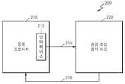
도 2a는 종래의 응용 프로세서 및 전압 조절 집적 회로를 구비하는 반도체 장치를 나타내는 도면이다.2A is a diagram showing a semiconductor device having a conventional application processor and a voltage regulation integrated circuit.
도 2a를 참조하면, 반도체 장치(200)는 응용 프로세서(210) 및 전압 조절 집적 회로(220)를 구비한다. 그리고, 응용 프로세서(210)는 내부적으로 인터페이스(interface)(212)를 구비한다.Referring to FIG. 2A, the
도시된 응용 프로세서(210)는 모바일 시스템에서 필요로 하는 모든 응용 프로세서들이 될 수 있다. 응용 프로세서의 정의 및 종류 등은 본 발명이 속하는 기술 분야에서 통상의 지식을 가진 자에게 있어서 자명한 것이므로, 상세한 설명은 생략하도록 한다.The illustrated
응용 프로세서(210)의 내부에 구비되는 인터페이스(212)의 종류로는 IIC(Inter Integrated Circuit)(또는 I2C라고도 함), SPI(Serial Peripheral Interface), GPIO(General Purpose Input/Output) 등이 있다.The
응용 프로세서(210)는 IIC, SPI, 또는 GPIO 등으로 이루어지는 인터페이스(212)를 통하여 전압 조절 집적 회로(220)의 전압 레벨 값을 제어(control)한다. 여기서, IIC, SPI, 또는 GPIO 등으로 이루어지는 인터페이스는 특정 동작(예를 들어, 전압 레벨 값을 변경하여 설정하는 동작)을 수행하는데 있어서, 소프트웨어적인 제어(software control)를 추가로 필요로 한다.The
전압 조절 집적 회로(220)는 응용 프로세서(210)의 제어에 응답하여, 코어 클럭 레벨의 변화에 상응하여 변경된 전압 레벨 값을 갖는 전압을 발생시킨다.In response to control of the
응용 프로세서(210)의 동작 주파수가 변화하게 되면, 인터페이스(212)는 동작 주파수 변화에 맞춰서 동작 전압 값을 새로이 설정한다. 그리고, 새로이 설정된 동작 전압 값을 전압 조절 집적 회로(220)로 전송한다. 여기서, 새로이 설정된 동작 전압 값의 전송은 214 신호선을 통하여 이루어진다. 214 신호선은 인터페이스(212)와 전압 조절 집적 회로(220)를 연결하는 신호선으로, 동작 전압의 전압 레벨 값을 전송하기 위한 신호선이 되다.When the operating frequency of the
전압 조절 집적 회로(220)는 인터페이스(212)로부터 전송받은 동작 전압의 전압 레벨 값에 응답하여, 상기 전압 레벨 값을 갖는 동작 전압을 생성 및 출력한다. 216 신호선은, 전압 조절 집적 회로(220)에서 생성된 동작 전압을 응용 프로세서(210)로 전송하는데 필요한 전압 공급 신호선이 된다.The voltage regulation integrated
여기서, 인터페이스(212)가 동작 전압의 전압 레벨 값을 변경하여 설정하는데 에는 일정 시간이 소요되게 된다. 이하에서는, (인터페이스가 동작 전압의 전압 레벨을 변경 설정하는데 일정 시간이 소요됨에 따라서), 클럭 주파수 변화에 따른 공급 전압의 변화를 도 2b를 참조하여 설명하도록 한다.Here, it takes a certain time for the
도 2b는 도 2a의 응용 프로세서에 있어서, 클럭 주파수 변화에 따른 공급 전압의 변화를 나타내는 그래프이다.FIG. 2B is a graph showing a change in supply voltage according to a clock frequency change in the application processor of FIG. 2A. FIG.
도 2b를 참조하면, 252, 254, 및 256 구간은 각각 코어 클럭 레벨이 600MHz, 200MHz, 및 600MHz 인 구간을 나타낸다.Referring to FIG. 2B, the
도 1에서 설명하였던 바와 같이 모바일 시스템이 전력 소모 절약을 위하여 이상적으로 동작하는 경우, 동작 전압은 260 곡선에서와 같이 변화한다.As described in FIG. 1, when the mobile system operates ideally for saving power consumption, the operating voltage changes as in the
그러나, 종래의 반도체 장치는 전술한 인터페이스(212)의 소프트웨어적 제어 동작으로 인하여, 코어 클럭 레벨이 변화하여도 동작 전압을 즉각적으로 변화시키지 못한다. 즉, 인터페이스 장치의 소프트웨어적 제어 동작(코어 클럭 레벨 변화에 따라서, 새롭게 동작 전압의 전압 레벨 값을 설정하고, 설정된 값을 전압 조절 집적 회로(220)로 전송하는 동작)에는 소정 시간이 소요되게 된다.However, due to the software control operation of the above-described
도 2b를 참조하면, t11 시점에서 코어 클럭 레벨(250)이 600MHz에서 200MHz로 변화하였다. 그러나, 동작 전압은 t11 시점을 기준으로 200us가 지난 후인 t11 시점에서 변화하게 된다. 따라서, t11 시점에서 t13 시점 구간동안에는 0.9V의 동작 전압만이 공급되면 족하나, 종래의 반도체 장치에서는 1.1V의 동작 전압이 공급되게 되어 t11 시점부터 t13시점 동안에 불필요한 전력 소모가 발생하게 된다.Referring to FIG. 2B, at time t11, the
또한, 종래의 반도체 장치에서는 코어 클럭 레벨이 200MHz에서 600MHz로 변화하는 시점(t12) 이전에, 동작 전압(260)을 0.9V에서 다시 1.1V로 변화시켜야 한다. 종래의 반도체 장치에서는, t12 시점 이후에(코어 클럭 레벨이 600MHz가 되는 시점 이전에) 0.9V의 전압이 공급되는 것을 방지하기 위하여, t12 시점 이전에 공급 전압 값을 0.9V에서 1.1V로 승압하게 된다. 즉, t12 시점에 앞서서 t14 시점에서 공급 전압 값이 0.9V에서 1.1V로 변화되는 것이다. 그에 따라서, t14 시점부터 t12시점 동안에 불필요한 전력 소모가 발생하게 된다.In the conventional semiconductor device, the
본 발명이 이루고자 하는 기술적 과제는 동작 클럭 신호의 주파수 변화에 따라서 즉각적이고 유연하게 코어 전압을 변경시킬 수 있는 전력 조절 집적 회로를 포함하는 반도체 장치를 제공하는데 있다.SUMMARY OF THE INVENTION It is an object of the present invention to provide a semiconductor device including a power control integrated circuit capable of instantly and flexibly changing a core voltage according to a frequency change of an operation clock signal.
본 발명의 일 실시예에 따른 반도체 장치는 응용 프로세서 및 전압 조절 집적 회로를 구비한다.A semiconductor device according to an embodiment of the present invention includes an application processor and a voltage regulation integrated circuit.
응용 프로세서는 동작 클럭 신호에 대한 정보인 클럭 정보를 출력한다.The application processor outputs clock information, which is information on the operating clock signal.
전압 조절 집적 회로는 상기 클럭 정보를 전송받고, 그에 응답하여 상기 정보에 대응되는 전압 레벨 값을 갖는 코어 전압을 생성 및 출력한다.The voltage modulating integrated circuit receives the clock information and responsively generates and outputs a core voltage having a voltage level value corresponding to the information.
상기 동작 클럭 신호는 상기 응용 프로세서의 내부적에 구비되는 코어 회로의 동작을 위해 공급되는 클럭 신호로, 변화하는 주파수 값을 갖는 신호이다.The operation clock signal is a clock signal supplied for operation of a core circuit provided internally to the application processor, and is a signal having a changing frequency value.
바람직하게, 상기 클럭 정보는 상기 동작 클럭 신호 자체, 또는 상기 동작 클럭 신호의 주파수 또는 주기 값을 포함 정보 신호일 수 있다.Preferably, the clock information may be an information signal comprising the operating clock signal itself, or the frequency or period value of the operating clock signal.
바람직하게, 상기 전력 조절 집적 회로는 상기 클럭 정보를 전송받고, 그에 응답하여 먹스 선택 신호를 발생시키는 클럭 정보 감지 회로, 및 상기 먹스 선택 신호에 응답해, 상기 응용 프로세서에서 이용하는 다수개의 전압 레벨 값들 중 어느 하나를 선택하여 상기 코어 전압으로써 생성하는 전압 생성 장치를 구비할 수 있다.Preferably, the power conditioning integrated circuit includes a clock information sensing circuit for receiving the clock information and generating a mux select signal in response thereto, and a clock signal sensing circuit responsive to the mux select signal for selecting among a plurality of voltage level values And a voltage generator for generating the core voltage by selecting any one of the plurality of voltages.
바람직하게, 상기 클럭 정보 감지 회로는 상기 클럭 정보를 이용해 상기 동작 클럭 신호의 주파수 값을 감지하고, 상기 감지된 주파수 값에 상응하는 먹스 선택 신호를 출력한다.Preferably, the clock information sensing circuit senses a frequency value of the operation clock signal using the clock information, and outputs a mux selection signal corresponding to the sensed frequency value.
바람직하게, 상기 전압 생성 장치는 선택부 및 전압 발생기를 구비할 수 있다. 선택기는 상기 다수개의 전압 레벨 값들을 저장하고, 상기 먹스 선택 신호에 응답하여 상기 다수개의 전압 레벨 값들 중 어느 하나를 선택하여 출력한다. 전압 발생기는 상기 선택된 전압 레벨 값을 갖는 전압을 생성하여 출력한다.Preferably, the voltage generation device may include a selection unit and a voltage generator. The selector stores the plurality of voltage level values and selects one of the plurality of voltage level values in response to the mux select signal. The voltage generator generates and outputs a voltage having the selected voltage level value.
바람직하게, 상기 선택부는 다수개의 저장 소자들을 포함하며, 상기 다수개의 저장 소자들 각각에 상기 다수개의 전압 레벨 값들을 저장하하는 저장 소자 어레이, 및 상기 먹스 선택 신호에 응답하여, 상기 저장 소자 어레이에 저장되어 있는 다수개의 전압 레벨 값들 중 어느 하나를 선택하여 출력하는 선택 소자를 구비할 수 있다.Advantageously, the selector comprises a storage element array including a plurality of storage elements, the storage element array storing the plurality of voltage level values in each of the plurality of storage elements, and the storage element array in response to the mux select signal, And a selection element for selecting and outputting any one of a plurality of stored voltage level values.
바람직하게, 상기 저장 소자들 각각은 레지스터로 이루어질 수 있다.Preferably, each of the storage elements may comprise a resistor.
바람직하게, 상기 선택 소자는 먹스로 이루어질 수 있다.Preferably, the selection element may comprise a mux.
바람직하게, 상기 응용 프로세서는 상기 다수개의 전압 레벨 값들을 설정하고, 상기 설정된 값들을 상기 저장 소자 어레이로 전송하여 저장시키는 인터페이스 회로를 더 구비할 수 있다.The application processor may further include an interface circuit for setting the plurality of voltage level values and transmitting the set values to the storage element array for storage.
바람직하게, 상기 응용 프로세서는 상기 동작 클럭 신호를 생성하는 클럭 발생부를 구비할 수 있다.Preferably, the application processor may include a clock generator for generating the operation clock signal.
바람직하게, 상기 클럭 발생부는 위상 동기 루프 회로로 이루어질 수 있다.Preferably, the clock generator may be a phase-locked loop circuit.
본 발명의 다른 실시예에 따른 전력 조절 집적 회로를 포함하는 반도체 장치는 응용 프로세서 및 전압 조절 집적 회로를 구비한다.A semiconductor device including a power conditioning integrated circuit according to another embodiment of the present invention includes an application processor and a voltage regulation integrated circuit.
응용 프로세서는 동작 클럭 신호에 대한 정보인 클럭 정보를 출력한다.The application processor outputs clock information, which is information on the operating clock signal.
전압 조절 집적 회로는 상기 클럭 정보에 응답하여 상기 클럭 정보에 대응되는 전압 레벨 값을 갖는 코어 전압을 생성 및 출력한다.The voltage controlling integrated circuit generates and outputs a core voltage having a voltage level value corresponding to the clock information in response to the clock information.
전압 조절 집적 회로는 상기 클럭 정보를 전송 받고, 그에 응답하여 먹스 선택 신호를 발생시키는 클럭 정보 감지 회로, 상기 응용 프로세서에서 이용되는 다수개의 전압 레벨 값들을 저장하고, 상기 먹스 선택 신호에 응답하여 상기 다수개의 전압 레벨 값들 중 어느 하나를 선택하여 출력하는 선택부, 및 상기 선택된 전압 레벨 값에 해당하는 전압을 생성하여 상기 응용 프로세서로 출력하는 전압 생성기를 구비한다.A voltage-controlled integrated circuit includes: a clock information sensing circuit for receiving the clock information and generating a mux select signal in response thereto; a memory for storing a plurality of voltage level values used in the application processor, And a voltage generator for generating a voltage corresponding to the selected voltage level value and outputting the generated voltage to the application processor.
바람직하게, 상기 동작 클럭 신호는 상기 응용 프로세서의 내부적에 구비되는 코어 회로의 동작을 위해 공급되는 클럭 신호로, 변화하는 주파수 값을 갖는 신호이다.Preferably, the operation clock signal is a clock signal supplied for operation of a core circuit provided internally to the application processor, and is a signal having a changing frequency value.
본 발명의 일 실시예에 따른 전력 조절 집적 회로를 포함하는 반도체 장치는 동작 클럭 신호의 주파수 변화에 따라서 즉각적이고 유연하게 코어 전압을 변경시킬 수 있다. 그에 따라서, 본 발명의 일 실시예에 따른 반도체 장치는 전력 소비를 감소시킬 수 있는 효과가 있다.The semiconductor device including the power control integrated circuit according to an embodiment of the present invention can change the core voltage instantaneously and flexibly according to the frequency change of the operation clock signal. Accordingly, the semiconductor device according to the embodiment of the present invention has the effect of reducing power consumption.
본 발명과 본 발명의 동작상의 이점 및 본 발명의 실시에 의하여 달성되는 목적을 충분히 이해하기 위해서는 본 발명의 바람직한 실시예를 예시하는 첨부 도면 및 도면에 기재된 내용을 참조하여야 한다.In order to fully understand the present invention, operational advantages of the present invention, and objects achieved by the practice of the present invention, reference should be made to the accompanying drawings and the accompanying drawings which illustrate preferred embodiments of the present invention.
이하, 첨부한 도면을 참조하여 본 발명이 바람직한 실시예를 설명함으로써, 본 발명을 상세히 설명한다. 각 도면에 제시된 동일한 참조부호는 동일한 부재를 나타낸다.DETAILED DESCRIPTION OF THE PREFERRED EMBODIMENTS Hereinafter, a preferred embodiment of the present invention will be described in detail with reference to the accompanying drawings. Like reference symbols in the drawings denote like elements.
도 3은 본 발명의 일 실시예에 따른 전압 조절 집적 회로를 구비하는 반도체 장치를 나타내는 도면이다.3 is a diagram showing a semiconductor device having a voltage-controlling integrated circuit according to an embodiment of the present invention.
도 3을 참조하면, 본 발명의 일 실시예에 따른 반도체 장치(300)는 응용 프로세서(310) 및 전압 조절 집적 회로(330)를 구비한다.3, a
응용 프로세서(310)는 동작 클럭 신호에 대한 정보인 클럭 정보를 출력한다. 여기서, 동작 클럭 신호는 응용 프로세서(310)의 내부적으로 구비되는 코어 회로(core circuit)(또는 코어 블록(core block)이라고 함)의 동작을 위해 공급되는 클럭 신호로, 변화하는 주파수 값을 갖는 신호가 된다. 예를 들어, 코어 블록은, 동작 클럭 신호에 동기화되어 명령어를 전송, 데이터를 기입 또는 독출하는 동작 등을 수행 할 수 있다. 코어 회로 및 응용 프로세서 자체의 정의 내용은 본 발명이 속하는 기술분야에서 통상의 지식을 가진 자에게 있어서 자명한 것이므로, 상세한 설명은 생략하도록 한다.The
그리고, 클럭 정보는 321 신호선을 통하여 전압 조절 집적 회로(330)로 전송될 수 있다.The clock information may be transmitted to the voltage regulation integrated
바람직하게, 클럭 정보는 동작 클럭 신호 자체가 될 수 있다. 또는, 클럭 정보는 동작 클럭 신호의 주파수 또는 주기 값을 포함하는 정보 신호이다.Preferably, the clock information may be the operating clock signal itself. Alternatively, the clock information is an information signal including the frequency or period value of the operation clock signal.
전압 조절 집적 회로(330)는 클럭 정보를 전송받고, 그에 응답하여 클럭 정보에 대응되는 전압 레벨 값을 갖는 코어 전압을 생성 및 출력한다. 코어 전압은 325 신호선을 통하여, 응용 프로세서(310)(구체적으로, 코어 회로(미도시))로 전송될 수 있다.The voltage regulating
응용 프로세서(310)는 내부적으로 인터페이스 회로(312), 및 인터페이스 회로(312)와 전압 조절 집적 회로(330)를 연결하는 신호선(323)을 더 구비할 수 있다. 이하에서는 도 4를 참조하여, 본 발명의 일 실시예에 따른 전력 조절 집적 회로를 포함하는 반도체 장치(300)를 상세히 설명하도록 한다.The
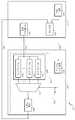
도 4는 도 3의 반도체 장치를 상세히 나타내는 도면이다.4 is a detailed view of the semiconductor device of FIG.
도 4를 참조하면, 전력 조절 집적 회로(330)는 클럭 정보 감지 회로(450), 및 전압 생성 장치(460)를 포함할 수 있다.Referring to FIG. 4, the power conditioning integrated
클럭 정보 감지 회로(450)는 클럭 정보를 전송받고, 그에 응답하여 먹스 선택 신호(S_SEL)를 발생시킨다. The clock
전술한 바와 같이, 클럭 정보는 동작 클럭 신호 자체가 될 수 있다. 또는, 클럭 정보는 동작 클럭 신호의 주파수 또는 주기 값을 포함하는 정보 신호가 될 수 있다. 바람직하게, 클럭 정보 감지 회로(450)는 전송받은 클럭 정보를 이용해 동작 클럭 신호의 주파수를 감지하고, 감지된 주파수 값에 상응하는 먹스 선택 신호를 발생시켜 출력한다.As described above, the clock information may be the operation clock signal itself. Alternatively, the clock information may be an information signal comprising the frequency or period value of the operating clock signal. Preferably, the clock
전압 생성 장치(460)는 먹스 선택 신호(S_SEL)에 응답해, 응용 프로세서(310)에서 이용하는 다수개의 전압 레벨 값들 중 어느 하나를 선택하고, 이를 코어 전압으로써 생성한다.In response to the mux select signal S_SEL, the
바람직하게, 전압 생성 장치(460)는 선택부(470) 및 전압 발생기(490)를 구비할 수 있다.Preferably, the
선택부(470)는 다수개의 전압 레벨 값들을 저장하고, 먹스 선택 신호에 응답하여 대수개의 전압 레벨 값들 중 어느 하나를 선택하여 출력한다.The
바람직하게, 선택부(470)는 저장 소자 어레이(480) 및 선택 소자(471)를 구비할 수 있다.Preferably, the
저장 소자 어레이(480)는 다수개의 저장 소자들(481, 482, 483)을 포함하며, 상기 다수개의 저장 소자들 각각에 다수개의 전압 레벨 값들을 저장한다. 저장 소자들 각각은 레지스터(register) 등을 포함하는 단위 메모리 장치로 이루어질 수 있다.The
선택 소자(471)는 먹스 선택 신호(S_SEL)에 응답하여, 저장 소자 어레이(480)에 저장되어 있는 다수개의 전압 레벨 값들 중 어느 하나를 선택하여 출력한다. 선택 소자(471)는 먹스(MUX: multiplexer)와 같은 단순 선택 소자로 이루어질 수 있다.The
전압 발생기(490)는 선택된 전압 레벨 값을 갖는 전압을 생성하여 출력한다. 예를 들어, 입력 데이터로 4 또는 6이 입력되면, 4V 또는 6V에 해당하는 전압을 생성하여 출력할 수 있다.The
인터페이스 회로(312)는 다수개의 전압 레벨 값들을 설정하고, 설정된 값들을 저장 소자 어레이(480)로 전송하여 저장시킨다. 여기서, '다수개의 전압 레벨 값들'은 응용 프로세서(310)의 코어 회로(420)에서 이용하는 전압 레벨들을 가리킨다. 코어 회로(420)의 동작 전압은 고정된 값을 갖는 것이 아니며, 동작 클럭 신호의 주파수(frequency)에 따라서 다양한 전압 값을 가질 있다.The
예를 들어, 600MHz의 주파수를 갖는 동작 클럭 신호에서는 1.1V의 동작 전압만이 공급되면 되고, 200MHz의 주파수를 갖는 동작 클럭 신호에서는 0.9V의 동작 전압만이 공급되면 족하다. 즉, 코어 회로(420)는 동작 클럭 신호의 동작 주파수 변화에 따라서 다양한 동작 전압들을 이용하게 되며, 이 때 이용되는 동작 전압의 값들이 '다수개의 전압 레벨 값들'인 것이다.For example, an operating clock signal having a frequency of 600 MHz needs only to be supplied with an operating voltage of 1.1 V, and an operating clock signal having a frequency of 200 MHz requires only an operating voltage of 0.9 V to be supplied. That is, the
여기서, 다수개의 전압 레벨 값들을 각각의 코어 회로 또는 응용 프로세서의 제작 사양 등에 달라지게 된다.Here, the plurality of voltage level values are different from each other in the manufacturing specifications of each core circuit or application processor.
도 4를 참조하면, 응용 프로세서(310)는 클럭 발생부(410), 코어 회로(420), 또는 인터페이스 회로(312)를 포함할 수 있다.Referring to FIG. 4, the
클럭 발생부(410)는 동작 클럭 신호를 생성한다. 클럭 발생부(410)는 위상 동기 루프 회로(PLL: Phase Locked Loop), 지연 동기 루프(DLL: Delayed Locked Loop), 수정자(Crystal)등의 클럭 생성 장치로 이루어질 수 있다.The
코어 회로(420)는 동작 클럭 신호 및 코어 전압을 전송받고, 동작 클럭 신호에 동기화하여 동작한다. 또는, 동작 클럭 신호에 비동기화하여 동작할 수 도 있다. 동작 클럭 신호는 클럭 발생부(410)로부터 전송되고, 코어 전압은 전압 발생 기(490)로부터 전송된다.The
인터페이스 회로(312)는 IIC(Inter Integrated Circuit)(또는 I2C라고도 함), SPI(Serial Peripheral Interface), GPIO(General Purpose Input/Output) 등의 현존하는 모든 인터페이스 장치가 될 수 있다.The
본원에서는, 인터페이스 회로(312)가 변화하는 동작 클럭의 주파수에 맞춰서, 매번 서로 다른 전압 레벨 값을 세팅하는 것이 아니다. 인터페이 회로(312)에서는, 본원의 반도체 장치(400)에 구비되는 인터페이스 회로(312)는 코어 회로에서 이용되는 전압 레벨 값을 설정하여 저장 소자 어레이(480)로 전송 및 저장시키게 된다. 도 1의 경우를 예로 들어 설명하면, 저장 소자 어레이(480)는 1.1, 0.9 등의 전압 값을 모두 저장시켜 놓는다.In the present application, the
본 발명의 일 실시예에 따른 반도체 장치(400)의 전체적인 동작을 보면, 인터페이스 회로(312)는 코어 회로(420)에서 이용되는 다수개의 전압 레벨들을 모두 설정하여 전압 발생 장치(460)(구체적으로, 저장 소자 어레이(480))에 저장시켜 놓는다. 클럭 발생부(410)에서 클럭 정보를 계속하여 클럭 정보 감지 회로(450)로 전송하므로, 클럭 정보 감지 회로(450)는 전송받은 클럭 정보를 이용하여, 계속하여 동작 클럭 신호의 주파수를 감지한다.The overall operation of the
그에 따라서, 클럭 정보 감지 회로(450)는 감지된 주파수에 대응되는 먹스 선택 신호(S_SEL)를 출력한다. 도 1을 참조하여 설명하면, 클럭 정보 감지 회로(450)가 600MHz의 주파수를 감지하면, 클럭 정보 감지 회로(450)는 저장 소자 어레이(480)에 저장된 전압 레벨 값들 중 1.1 값이 선택되도록 하는 먹스 선택 신 호(S_SEL)를 출력한다. 또 다른 예로, 200MHz의 주파수를 감지하였다면, 클럭 정보 감지 회로(450)는 0.9 값이 선택되로록 하는 먹스 선택 신호(S_SEL)를 출력한다.Accordingly, the clock
바람직하게, 클럭 정보는 인터페이스 회로(312)와 저장 소자 어레이(480)를 연결하는 신호선(323)과 구별되는 별도의 신호선(321)을 통하여 전송된다. 여기서, 별도의 신호선(321)은 클럭 출력 패드(clock out pad: 클럭 신호가 출력되는 단자) 핀(pin)과 연결된 신호선이 될 수 있다.The clock information is transmitted through a
상술한 바와 같이, 본 발명의 일 실시예에 따른 반도체 장치(400)는 전압 조절 집적 회로(330)에서 클럭 정보를 바로 입력받고, 그에 상응하는 전압 레벨 값을 선택하여 생성시킨다. 따라서, 동작 클럭 신호의 주파수가 변화하는 경우, 즉각적이고 유연하게 동작 전압을 변경하여 생성시킬 수 있다.As described above, the
따라서, 도 2b에서 설명된 t11 내지 t13 구간, 및 t14 내지 t12 구간에서 발생하는 전력 소모(불필요한 고 전류 이용에 따른 전력 소비 증가)를 제거할 수 있게 된다.Therefore, it is possible to eliminate the power consumption (increase in power consumption due to the unnecessary use of the high current) occurring in the t11 to t13 section and the t14 to t12 section described in Fig. 2B.
이상에서와 같이 도면과 명세서에서 최적 실시예가 개시되었다. 여기서 특정한 용어들이었으나, 이는 단지 본 발명을 설명하기 위한 목적에서 사용된 것이지 의미한정이나 특허청구범위에 기재된 본 발명의 범위를 제한하기 위하여 사용된 것은 아니다. 그러므로 본 기술분야의 통상의 지식을 가진 자라면 이로부터 다양한 변형 및 균등한 타 실시예가 가능하다는 점을 이해할 것이다. 따라서, 본 발명의 진정한 기술적 보호범위는 첨부된 특허청구범위의 기술적 사상에 의해 정해져야 할 것이다.As described above, an optimal embodiment has been disclosed in the drawings and specification. Although specific terms are employed herein, they are used for purposes of describing the present invention only and are not used to limit the scope of the present invention. Therefore, those skilled in the art will appreciate that various modifications and equivalent embodiments are possible without departing from the scope of the present invention. Accordingly, the true scope of the present invention should be determined by the technical idea of the appended claims.
도 1은 응용 프로세서에 있어서, 클럭 주파수 변화에 따른 공급 전압의 변화를 나타내는 그래프이다.1 is a graph showing a change in supply voltage according to a clock frequency change in an application processor.
도 2a는 종래의 응용 프로세서 및 전압 조절 집적 회로를 구비하는 반도체 장치를 나타내는 도면이다.2A is a diagram showing a semiconductor device having a conventional application processor and a voltage regulation integrated circuit.
도 2b는 도 2a의 응용 프로세서에 있어서, 클럭 주파수 변화에 따른 공급 전압의 변화를 나타내는 그래프이다.FIG. 2B is a graph showing a change in supply voltage according to a clock frequency change in the application processor of FIG. 2A. FIG.
도 3은 본 발명의 일 실시예에 따른 전압 조절 집적 회로를 구비하는 반도체 장치를 나타내는 도면이다.3 is a diagram showing a semiconductor device having a voltage-controlling integrated circuit according to an embodiment of the present invention.
도 4는 도 3의 반도체 장치를 상세히 나타내는 도면이다.4 is a detailed view of the semiconductor device of FIG.
Claims (17)
Translated fromKoreanPriority Applications (2)
| Application Number | Priority Date | Filing Date | Title |
|---|---|---|---|
| KR1020080029328AKR101452958B1 (en) | 2008-03-28 | 2008-03-28 | A semiconductor device including a power conditioning integrated circuit |
| US12/408,201US8135968B2 (en) | 2008-03-28 | 2009-03-20 | Semiconductor apparatus including power management integrated circuit |
Applications Claiming Priority (1)
| Application Number | Priority Date | Filing Date | Title |
|---|---|---|---|
| KR1020080029328AKR101452958B1 (en) | 2008-03-28 | 2008-03-28 | A semiconductor device including a power conditioning integrated circuit |
Publications (2)
| Publication Number | Publication Date |
|---|---|
| KR20090103611A KR20090103611A (en) | 2009-10-01 |
| KR101452958B1true KR101452958B1 (en) | 2014-10-22 |
Family
ID=41118949
Family Applications (1)
| Application Number | Title | Priority Date | Filing Date |
|---|---|---|---|
| KR1020080029328AActiveKR101452958B1 (en) | 2008-03-28 | 2008-03-28 | A semiconductor device including a power conditioning integrated circuit |
Country Status (2)
| Country | Link |
|---|---|
| US (1) | US8135968B2 (en) |
| KR (1) | KR101452958B1 (en) |
Families Citing this family (6)
| Publication number | Priority date | Publication date | Assignee | Title |
|---|---|---|---|---|
| KR101003153B1 (en)* | 2009-05-15 | 2010-12-21 | 주식회사 하이닉스반도체 | Voltage stabilization circuit and semiconductor memory device using same |
| KR102032330B1 (en)* | 2014-06-20 | 2019-10-16 | 에스케이하이닉스 주식회사 | Semiconductor device and its global synchronous type dynamic voltage frequency scaling method |
| DE102015112253A1 (en) | 2014-08-26 | 2016-03-03 | Samsung Electronics Co., Ltd. | Integrated power management circuit, power management method, mobile device and clock setting method |
| KR102320399B1 (en) | 2014-08-26 | 2021-11-03 | 삼성전자주식회사 | Power management integrated circuit, mobile device having the same and clock adjusting method thereof |
| KR20170124017A (en) | 2016-04-29 | 2017-11-09 | 삼성전자주식회사 | Memory device adjusting operation voltage, application processor controlling memory device and operating method of memory device |
| KR102748164B1 (en)* | 2019-10-17 | 2024-12-31 | 삼성전자주식회사 | Electronic device including power management integrated circuit and method for recovering abnormal state of the electronic device |
Citations (4)
| Publication number | Priority date | Publication date | Assignee | Title |
|---|---|---|---|---|
| KR20000046807A (en)* | 1998-12-31 | 2000-07-25 | 김영환 | Voltage generator for plate |
| KR20040014300A (en)* | 2002-08-08 | 2004-02-14 | 후지쯔 가부시끼가이샤 | Semiconductor integrated circuit having controllable internal supply voltage |
| US20040103330A1 (en)* | 2002-11-25 | 2004-05-27 | Bonnett William B. | Adjusting voltage supplied to a processor in response to clock frequency |
| JP2005533296A (en) | 2001-10-25 | 2005-11-04 | インテル・コーポレーション | Power reduction method and system |
Family Cites Families (5)
| Publication number | Priority date | Publication date | Assignee | Title |
|---|---|---|---|---|
| JPH0683988A (en) | 1992-09-01 | 1994-03-25 | Nec Corp | Microprocessor |
| US5504910A (en) | 1994-02-02 | 1996-04-02 | Advanced Micro Devices, Inc. | Power management unit including software configurable state register and time-out counters for protecting against misbehaved software |
| US5812860A (en)* | 1996-02-12 | 1998-09-22 | Intel Corporation | Method and apparatus providing multiple voltages and frequencies selectable based on real time criteria to control power consumption |
| US6425086B1 (en)* | 1999-04-30 | 2002-07-23 | Intel Corporation | Method and apparatus for dynamic power control of a low power processor |
| JP3864859B2 (en) | 2002-06-24 | 2007-01-10 | 株式会社日立製作所 | Semiconductor device or program for reducing power consumption of the semiconductor device |
- 2008
- 2008-03-28KRKR1020080029328Apatent/KR101452958B1/enactiveActive
- 2009
- 2009-03-20USUS12/408,201patent/US8135968B2/enactiveActive
Patent Citations (4)
| Publication number | Priority date | Publication date | Assignee | Title |
|---|---|---|---|---|
| KR20000046807A (en)* | 1998-12-31 | 2000-07-25 | 김영환 | Voltage generator for plate |
| JP2005533296A (en) | 2001-10-25 | 2005-11-04 | インテル・コーポレーション | Power reduction method and system |
| KR20040014300A (en)* | 2002-08-08 | 2004-02-14 | 후지쯔 가부시끼가이샤 | Semiconductor integrated circuit having controllable internal supply voltage |
| US20040103330A1 (en)* | 2002-11-25 | 2004-05-27 | Bonnett William B. | Adjusting voltage supplied to a processor in response to clock frequency |
Also Published As
| Publication number | Publication date |
|---|---|
| KR20090103611A (en) | 2009-10-01 |
| US8135968B2 (en) | 2012-03-13 |
| US20090249088A1 (en) | 2009-10-01 |
Similar Documents
| Publication | Publication Date | Title |
|---|---|---|
| KR101452958B1 (en) | A semiconductor device including a power conditioning integrated circuit | |
| CN107835988B (en) | Low power clock timing for high speed memory interface | |
| US8144529B2 (en) | System and method for delay locked loop relock mode | |
| JP5159316B2 (en) | On-demand power management method and equipment | |
| US7337335B2 (en) | Method and apparatus for on-demand power management | |
| US8200852B2 (en) | Multi-mode dongle for peripheral devices and associated methods | |
| EP1876509A1 (en) | Card electronic device and host device | |
| CN108028068A (en) | Voltage level detection and analog circuit layout for memory systems | |
| CN111406254B (en) | Configurable data refresh from volatile memory to non-volatile memory | |
| US20080155143A1 (en) | Usb device and peripheral device | |
| US20070058464A1 (en) | Semiconductor storage device, electronic apparatus, and mode setting method | |
| EP4339739A2 (en) | Power management integrated circuit, electronic device having the same, and operating method thereof | |
| US20210305939A1 (en) | Fast start-up crystal oscillator | |
| KR20160143159A (en) | Power Gating Control Circuit For Controlling Stably Data Restoring | |
| US9537484B2 (en) | Semiconductor device and method of controlling the same | |
| US20230198384A1 (en) | Device, system and method for providing a mode to control a switched-capacitor voltage regulator | |
| US8823428B2 (en) | Semiconductor device, method for operating the same, and memory system including the same | |
| JP4070924B2 (en) | IC card and terminal device thereof | |
| US8495409B2 (en) | Host controller, semiconductor device and method for setting sampling phase | |
| US8639952B1 (en) | Field-programmable gate array having voltage identification capability | |
| US20090121757A1 (en) | Data center tracking circuit and semiconductor integrated circuit including the same | |
| KR100849215B1 (en) | Power control apparatus, method, and system thereof | |
| CN1332287C (en) | Frequency voltage device for power management and method for frequency voltage control | |
| KR102076328B1 (en) | A method for power saving of computer system by using network signals | |
| KR101027700B1 (en) | Internal voltage generation circuit and semiconductor device using same |
Legal Events
| Date | Code | Title | Description |
|---|---|---|---|
| PA0109 | Patent application | Patent event code:PA01091R01D Comment text:Patent Application Patent event date:20080328 | |
| PG1501 | Laying open of application | ||
| A201 | Request for examination | ||
| PA0201 | Request for examination | Patent event code:PA02012R01D Patent event date:20130114 Comment text:Request for Examination of Application Patent event code:PA02011R01I Patent event date:20080328 Comment text:Patent Application | |
| E902 | Notification of reason for refusal | ||
| PE0902 | Notice of grounds for rejection | Comment text:Notification of reason for refusal Patent event date:20140128 Patent event code:PE09021S01D | |
| E701 | Decision to grant or registration of patent right | ||
| PE0701 | Decision of registration | Patent event code:PE07011S01D Comment text:Decision to Grant Registration Patent event date:20140714 | |
| GRNT | Written decision to grant | ||
| PR0701 | Registration of establishment | Comment text:Registration of Establishment Patent event date:20141014 Patent event code:PR07011E01D | |
| PR1002 | Payment of registration fee | Payment date:20141015 End annual number:3 Start annual number:1 | |
| PG1601 | Publication of registration | ||
| FPAY | Annual fee payment | Payment date:20180927 Year of fee payment:5 | |
| PR1001 | Payment of annual fee | Payment date:20180927 Start annual number:5 End annual number:5 | |
| FPAY | Annual fee payment | Payment date:20190930 Year of fee payment:6 | |
| PR1001 | Payment of annual fee | Payment date:20190930 Start annual number:6 End annual number:6 | |
| PR1001 | Payment of annual fee | Payment date:20210929 Start annual number:8 End annual number:8 | |
| PR1001 | Payment of annual fee | Payment date:20220927 Start annual number:9 End annual number:9 | |
| PR1001 | Payment of annual fee | Payment date:20240925 Start annual number:11 End annual number:11 |