KR101448908B1 - Semiconductor device - Google Patents
Semiconductor deviceDownload PDFInfo
- Publication number
- KR101448908B1 KR101448908B1KR1020137009129AKR20137009129AKR101448908B1KR 101448908 B1KR101448908 B1KR 101448908B1KR 1020137009129 AKR1020137009129 AKR 1020137009129AKR 20137009129 AKR20137009129 AKR 20137009129AKR 101448908 B1KR101448908 B1KR 101448908B1
- Authority
- KR
- South Korea
- Prior art keywords
- transistor
- electrode
- oxide semiconductor
- insulating layer
- drain electrode
- Prior art date
- Legal status (The legal status is an assumption and is not a legal conclusion. Google has not performed a legal analysis and makes no representation as to the accuracy of the status listed.)
- Expired - Fee Related
Links
Images


Classifications
- H—ELECTRICITY
- H01—ELECTRIC ELEMENTS
- H01L—SEMICONDUCTOR DEVICES NOT COVERED BY CLASS H10
- H01L21/00—Processes or apparatus adapted for the manufacture or treatment of semiconductor or solid state devices or of parts thereof
- H01L21/02—Manufacture or treatment of semiconductor devices or of parts thereof
- H01L21/02104—Forming layers
- H01L21/02365—Forming inorganic semiconducting materials on a substrate
- H01L21/02518—Deposited layers
- H01L21/02521—Materials
- H01L21/02551—Group 12/16 materials
- H01L21/02554—Oxides
- H—ELECTRICITY
- H10—SEMICONDUCTOR DEVICES; ELECTRIC SOLID-STATE DEVICES NOT OTHERWISE PROVIDED FOR
- H10B—ELECTRONIC MEMORY DEVICES
- H10B41/00—Electrically erasable-and-programmable ROM [EEPROM] devices comprising floating gates
- H10B41/30—Electrically erasable-and-programmable ROM [EEPROM] devices comprising floating gates characterised by the memory core region
- G—PHYSICS
- G11—INFORMATION STORAGE
- G11C—STATIC STORES
- G11C11/00—Digital stores characterised by the use of particular electric or magnetic storage elements; Storage elements therefor
- G11C11/21—Digital stores characterised by the use of particular electric or magnetic storage elements; Storage elements therefor using electric elements
- G11C11/34—Digital stores characterised by the use of particular electric or magnetic storage elements; Storage elements therefor using electric elements using semiconductor devices
- G11C11/40—Digital stores characterised by the use of particular electric or magnetic storage elements; Storage elements therefor using electric elements using semiconductor devices using transistors
- G11C11/401—Digital stores characterised by the use of particular electric or magnetic storage elements; Storage elements therefor using electric elements using semiconductor devices using transistors forming cells needing refreshing or charge regeneration, i.e. dynamic cells
- G11C11/403—Digital stores characterised by the use of particular electric or magnetic storage elements; Storage elements therefor using electric elements using semiconductor devices using transistors forming cells needing refreshing or charge regeneration, i.e. dynamic cells with charge regeneration common to a multiplicity of memory cells, i.e. external refresh
- H—ELECTRICITY
- H01—ELECTRIC ELEMENTS
- H01L—SEMICONDUCTOR DEVICES NOT COVERED BY CLASS H10
- H01L21/00—Processes or apparatus adapted for the manufacture or treatment of semiconductor or solid state devices or of parts thereof
- H01L21/02—Manufacture or treatment of semiconductor devices or of parts thereof
- H01L21/02104—Forming layers
- H01L21/02365—Forming inorganic semiconducting materials on a substrate
- H01L21/02518—Deposited layers
- H01L21/02521—Materials
- H01L21/02565—Oxide semiconducting materials not being Group 12/16 materials, e.g. ternary compounds
- H—ELECTRICITY
- H01—ELECTRIC ELEMENTS
- H01L—SEMICONDUCTOR DEVICES NOT COVERED BY CLASS H10
- H01L21/00—Processes or apparatus adapted for the manufacture or treatment of semiconductor or solid state devices or of parts thereof
- H01L21/02—Manufacture or treatment of semiconductor devices or of parts thereof
- H01L21/02104—Forming layers
- H01L21/02365—Forming inorganic semiconducting materials on a substrate
- H01L21/02612—Formation types
- H01L21/02617—Deposition types
- H01L21/02631—Physical deposition at reduced pressure, e.g. MBE, sputtering, evaporation
- H—ELECTRICITY
- H01—ELECTRIC ELEMENTS
- H01L—SEMICONDUCTOR DEVICES NOT COVERED BY CLASS H10
- H01L21/00—Processes or apparatus adapted for the manufacture or treatment of semiconductor or solid state devices or of parts thereof
- H01L21/02—Manufacture or treatment of semiconductor devices or of parts thereof
- H01L21/02104—Forming layers
- H01L21/02365—Forming inorganic semiconducting materials on a substrate
- H01L21/02656—Special treatments
- H01L21/02664—Aftertreatments
- H—ELECTRICITY
- H10—SEMICONDUCTOR DEVICES; ELECTRIC SOLID-STATE DEVICES NOT OTHERWISE PROVIDED FOR
- H10B—ELECTRONIC MEMORY DEVICES
- H10B41/00—Electrically erasable-and-programmable ROM [EEPROM] devices comprising floating gates
- H10B41/10—Electrically erasable-and-programmable ROM [EEPROM] devices comprising floating gates characterised by the top-view layout
- H—ELECTRICITY
- H10—SEMICONDUCTOR DEVICES; ELECTRIC SOLID-STATE DEVICES NOT OTHERWISE PROVIDED FOR
- H10B—ELECTRONIC MEMORY DEVICES
- H10B41/00—Electrically erasable-and-programmable ROM [EEPROM] devices comprising floating gates
- H10B41/20—Electrically erasable-and-programmable ROM [EEPROM] devices comprising floating gates characterised by three-dimensional arrangements, e.g. with cells on different height levels
- H—ELECTRICITY
- H10—SEMICONDUCTOR DEVICES; ELECTRIC SOLID-STATE DEVICES NOT OTHERWISE PROVIDED FOR
- H10B—ELECTRONIC MEMORY DEVICES
- H10B41/00—Electrically erasable-and-programmable ROM [EEPROM] devices comprising floating gates
- H10B41/30—Electrically erasable-and-programmable ROM [EEPROM] devices comprising floating gates characterised by the memory core region
- H10B41/35—Electrically erasable-and-programmable ROM [EEPROM] devices comprising floating gates characterised by the memory core region with a cell select transistor, e.g. NAND
- H—ELECTRICITY
- H10—SEMICONDUCTOR DEVICES; ELECTRIC SOLID-STATE DEVICES NOT OTHERWISE PROVIDED FOR
- H10B—ELECTRONIC MEMORY DEVICES
- H10B41/00—Electrically erasable-and-programmable ROM [EEPROM] devices comprising floating gates
- H10B41/70—Electrically erasable-and-programmable ROM [EEPROM] devices comprising floating gates the floating gate being an electrode shared by two or more components
- H—ELECTRICITY
- H10—SEMICONDUCTOR DEVICES; ELECTRIC SOLID-STATE DEVICES NOT OTHERWISE PROVIDED FOR
- H10D—INORGANIC ELECTRIC SEMICONDUCTOR DEVICES
- H10D86/00—Integrated devices formed in or on insulating or conducting substrates, e.g. formed in silicon-on-insulator [SOI] substrates or on stainless steel or glass substrates
- H10D86/201—Integrated devices formed in or on insulating or conducting substrates, e.g. formed in silicon-on-insulator [SOI] substrates or on stainless steel or glass substrates the substrates comprising an insulating layer on a semiconductor body, e.g. SOI
- H—ELECTRICITY
- H10—SEMICONDUCTOR DEVICES; ELECTRIC SOLID-STATE DEVICES NOT OTHERWISE PROVIDED FOR
- H10D—INORGANIC ELECTRIC SEMICONDUCTOR DEVICES
- H10D86/00—Integrated devices formed in or on insulating or conducting substrates, e.g. formed in silicon-on-insulator [SOI] substrates or on stainless steel or glass substrates
- H10D86/40—Integrated devices formed in or on insulating or conducting substrates, e.g. formed in silicon-on-insulator [SOI] substrates or on stainless steel or glass substrates characterised by multiple TFTs
- H10D86/421—Integrated devices formed in or on insulating or conducting substrates, e.g. formed in silicon-on-insulator [SOI] substrates or on stainless steel or glass substrates characterised by multiple TFTs having a particular composition, shape or crystalline structure of the active layer
- H10D86/423—Integrated devices formed in or on insulating or conducting substrates, e.g. formed in silicon-on-insulator [SOI] substrates or on stainless steel or glass substrates characterised by multiple TFTs having a particular composition, shape or crystalline structure of the active layer comprising semiconductor materials not belonging to the Group IV, e.g. InGaZnO
- H—ELECTRICITY
- H10—SEMICONDUCTOR DEVICES; ELECTRIC SOLID-STATE DEVICES NOT OTHERWISE PROVIDED FOR
- H10D—INORGANIC ELECTRIC SEMICONDUCTOR DEVICES
- H10D86/00—Integrated devices formed in or on insulating or conducting substrates, e.g. formed in silicon-on-insulator [SOI] substrates or on stainless steel or glass substrates
- H10D86/40—Integrated devices formed in or on insulating or conducting substrates, e.g. formed in silicon-on-insulator [SOI] substrates or on stainless steel or glass substrates characterised by multiple TFTs
- H10D86/60—Integrated devices formed in or on insulating or conducting substrates, e.g. formed in silicon-on-insulator [SOI] substrates or on stainless steel or glass substrates characterised by multiple TFTs wherein the TFTs are in active matrices
- H—ELECTRICITY
- H10—SEMICONDUCTOR DEVICES; ELECTRIC SOLID-STATE DEVICES NOT OTHERWISE PROVIDED FOR
- H10D—INORGANIC ELECTRIC SEMICONDUCTOR DEVICES
- H10D88/00—Three-dimensional [3D] integrated devices
- G—PHYSICS
- G11—INFORMATION STORAGE
- G11C—STATIC STORES
- G11C11/00—Digital stores characterised by the use of particular electric or magnetic storage elements; Storage elements therefor
- G11C11/21—Digital stores characterised by the use of particular electric or magnetic storage elements; Storage elements therefor using electric elements
- G11C11/34—Digital stores characterised by the use of particular electric or magnetic storage elements; Storage elements therefor using electric elements using semiconductor devices
- G11C11/40—Digital stores characterised by the use of particular electric or magnetic storage elements; Storage elements therefor using electric elements using semiconductor devices using transistors
- G11C11/401—Digital stores characterised by the use of particular electric or magnetic storage elements; Storage elements therefor using electric elements using semiconductor devices using transistors forming cells needing refreshing or charge regeneration, i.e. dynamic cells
- G11C11/403—Digital stores characterised by the use of particular electric or magnetic storage elements; Storage elements therefor using electric elements using semiconductor devices using transistors forming cells needing refreshing or charge regeneration, i.e. dynamic cells with charge regeneration common to a multiplicity of memory cells, i.e. external refresh
- G11C11/405—Digital stores characterised by the use of particular electric or magnetic storage elements; Storage elements therefor using electric elements using semiconductor devices using transistors forming cells needing refreshing or charge regeneration, i.e. dynamic cells with charge regeneration common to a multiplicity of memory cells, i.e. external refresh with three charge-transfer gates, e.g. MOS transistors, per cell
- G—PHYSICS
- G11—INFORMATION STORAGE
- G11C—STATIC STORES
- G11C16/00—Erasable programmable read-only memories
- G11C16/02—Erasable programmable read-only memories electrically programmable
- G11C16/04—Erasable programmable read-only memories electrically programmable using variable threshold transistors, e.g. FAMOS
- G11C16/0408—Erasable programmable read-only memories electrically programmable using variable threshold transistors, e.g. FAMOS comprising cells containing floating gate transistors
- G11C16/0425—Erasable programmable read-only memories electrically programmable using variable threshold transistors, e.g. FAMOS comprising cells containing floating gate transistors comprising cells containing a merged floating gate and select transistor
Landscapes
- Engineering & Computer Science (AREA)
- Microelectronics & Electronic Packaging (AREA)
- Computer Hardware Design (AREA)
- General Physics & Mathematics (AREA)
- Manufacturing & Machinery (AREA)
- Physics & Mathematics (AREA)
- Condensed Matter Physics & Semiconductors (AREA)
- Power Engineering (AREA)
- Thin Film Transistor (AREA)
- Semiconductor Memories (AREA)
- Dram (AREA)
- Metal-Oxide And Bipolar Metal-Oxide Semiconductor Integrated Circuits (AREA)
- Electroluminescent Light Sources (AREA)
- Electrodes Of Semiconductors (AREA)
Abstract
Translated fromKoreanDescription
Translated fromKorean개시하는 발명은, 반도체 소자를 이용한 반도체 장치 및 그 제작 방법에 관한 것이다.The present invention relates to a semiconductor device using a semiconductor element and a manufacturing method thereof.
반도체 소자를 이용한 기억 장치는, 전력의 공급이 없어지면 기억 내용이 사라지는 휘발성 기억 장치와, 전력의 공급이 없어져도 기억 내용은 보유되는 불휘발성 기억 장치로 크게 구별된다.2. Description of the Related Art A storage device using a semiconductor device is roughly divided into a volatile storage device in which the storage content disappears when power is not supplied and a nonvolatile storage device in which the storage content is retained even if power supply is lost.
휘발성 기억 장치의 대표적인 예로서는, DRAM(Dynamic Random Access Memory)가 있다. DRAM은 기억 소자를 구성하는 트랜지스터를 선택하여 커패시터에 전하를 축적함으로써 정보를 기억한다.A representative example of the volatile memory device is a DRAM (Dynamic Random Access Memory). The DRAM stores information by selecting a transistor constituting a memory element and accumulating charges in the capacitor.
상술한 원리로부터, DRAM에서는 정보를 읽어내면 커패시터의 전하는 없어지게 되기 때문에, 데이터의 판독 후, 재차 정보를 기억하려면, 재차의 기입 동작이 필요하다. 또한, 기억 소자를 구성하는 트랜지스터에는 리크 전류가 존재하고, 트랜지스터가 선택되어 있지 않은 상황에서도 전하가 유출, 또는 유입되기 때문에, 데이터의 보유 기간이 짧다. 따라서, 소정의 주기로 재차의 기입 동작(리프레시 동작)이 필요하고, 소비 전력을 충분히 저감하는 것은 곤란하다. 또한, 전력의 공급이 없어지면 기억 내용이 없어지기 때문에, 장기간의 기억의 보유에는 자성 재료나 광학 재료를 이용한 다른 기억 장치가 필요하다.In view of the above-described principle, since reading of information from a DRAM results in loss of electric charge of the capacitor, a rewriting operation is required to store information again after reading the data. Further, since the leakage current is present in the transistor constituting the memory element and the charge flows out or flows even when the transistor is not selected, the data holding period is short. Therefore, a rewriting operation (refresh operation) is required in a predetermined cycle, and it is difficult to sufficiently reduce power consumption. Further, since the storage contents are lost when the supply of electric power is lost, another storage device using a magnetic material or optical material is required for long-term memory retention.
휘발성 기억 장치의 다른 예로서는 SRAM(Static Random Access Memory)이 있다. SRAM은 플립플롭 등의 회로를 이용하여 기억 내용을 보유하기 때문에, 리프레시 동작이 불필요하고, 이 점에서는 DRAM보다 유리하다. 그러나, 플립플롭 등의 회로를 이용하고 있기 때문에, 기억 용량당의 단가가 높아진다는 문제가 있다. 또한, 전력의 공급이 없어지면 기억 내용이 없어진다는 점에 대해서는 DRAM과 다른 점은 없다.Another example of the volatile memory device is a static random access memory (SRAM). Since the SRAM uses a circuit such as a flip-flop to retain the contents of the memory, the refresh operation is unnecessary, which is advantageous over the DRAM in this respect. However, since a circuit such as a flip-flop is used, there is a problem that the unit cost per storage capacity is increased. In addition, there is no difference from DRAM in that memory contents are lost when power supply is lost.
불휘발성 기억 장치의 대표예로서는, 플래시 메모리가 있다. 플래시 메모리는 트랜지스터의 게이트 전극과 채널 형성 영역과의 사이에 플로팅 게이트를 가지고, 이 플로팅 게이트에 전하를 보유시킴으로써 기억을 행하기 때문에, 데이터의 보유 기간은 매우 길고(반영구적), 휘발성 기억 장치에 필요한 리프레시 동작이 불필요하다는 이점을 가지고 있다(예를 들면, 특허문헌 1 참조).As a representative example of the nonvolatile memory device, there is a flash memory. Since the flash memory has a floating gate between the gate electrode of the transistor and the channel forming region and holds the charge by holding the floating gate, the data holding period is very long (semipermanent) and is required for the volatile memory device And the refresh operation is unnecessary (see, for example, Patent Document 1).
그러나, 기입 시에 생기는 터널 전류에 의해 기억 소자를 구성하는 게이트 절연층이 열화하기 때문에, 소정 횟수의 기입에 의해 기억 소자가 기능하지 않게 된다는 문제가 생긴다. 이 문제의 영향을 완화하기 위해, 예를 들면, 각 기억 소자의 기입 횟수를 균일화하는 방법이 채용되지만, 이것을 실현하기 위해서는, 복잡한 주변 회로가 필요하게 된다. 그리고, 이러한 방법을 채용하더라도, 근본적인 수명의 문제가 해소되는 것은 아니다. 즉, 플래시 메모리는 정보의 다시쓰기 빈도가 높은 용도에는 적합하지 않다.However, since the gate insulating layer constituting the memory element is deteriorated by the tunnel current generated at the time of writing, there arises a problem that the memory element does not function by a predetermined number of times of writing. In order to alleviate the influence of this problem, for example, a method of equalizing the number of times of writing to each memory element is adopted, but in order to realize this, a complicated peripheral circuit is required. Even if this method is adopted, the problem of the fundamental life span is not solved. That is, the flash memory is not suitable for applications in which information is frequently rewritten.
또한, 플로팅 게이트에 전하를 보유시키기 위해, 또는, 그 전하를 제거하기 위해서는, 높은 전압이 필요하다. 또한, 전하의 보유, 또는 제거를 위해서는 비교적 긴 시간을 필요로 하고, 기입, 소거의 고속화가 용이하지 않다는 문제도 있다.In addition, a high voltage is required to hold the charge on the floating gate, or to remove the charge. In addition, it takes a relatively long time to hold or remove charges, and there is also a problem that it is not easy to increase the speed of writing and erasing.
상술한 문제를 감안하여, 개시하는 발명의 일 양태에서는, 전력이 공급되지 않는 상황에서도 기억 내용의 보유가 가능하고, 또한, 기입 횟수에도 제한이 없는, 새로운 구조의 반도체 장치를 제공하는 것을 목적의 하나로 한다.SUMMARY OF THE INVENTION In view of the above problems, it is an object of the present invention to provide a semiconductor device with a novel structure which can retain storage contents even in a situation where power is not supplied, One.
본 발명의 일 양태는, 산화물 반도체를 이용하여 형성되는 트랜지스터와, 그 이외의 재료를 이용하여 형성되는 트랜지스터와의 적층 구조에 관한 반도체 장치이다. 예를 들면, 다음과 같은 구성을 채용할 수 있다.One aspect of the present invention is a semiconductor device relating to a lamination structure of a transistor formed using an oxide semiconductor and a transistor formed using another material. For example, the following configuration can be adopted.
본 발명의 일 양태는, 소스선과, 비트선과, 신호선과, 워드선을 가지는 반도체 장치이다. 소스선과 비트선의 사이에는, 복수의 메모리 셀이 직렬로 접속되고, 복수의 메모리 셀의 하나는, 제 1 게이트 전극, 제 1 소스 전극, 및 제 1 드레인 전극을 가지는 제 1 트랜지스터와, 제 2 게이트 전극, 제 2 소스 전극, 및 제 2 드레인 전극을 가지는 제 2 트랜지스터와, 용량 소자를 가진다. 제 1 트랜지스터는 반도체 재료를 포함하는 기판에 설치되고, 제 2 트랜지스터는 산화물 반도체층을 포함하여 구성된다. 제 1 게이트 전극과, 제 2 소스 전극 또는 제 2 드레인 전극의 한쪽과, 용량 소자의 전극의 한쪽은 서로 전기적으로 접속된다. 소스선과 제 1 소스 전극은 서로 전기적으로 접속되고, 비트선과 제 1 드레인 전극은 서로 전기적으로 접속되고, 신호선과 제 2 게이트 전극은 서로 전기적으로 접속된다. 워드선과, 제 2 소스 전극 또는 제 2 드레인 전극의 다른 한쪽과 용량 소자의 전극의 다른 한쪽은 서로 전기적으로 접속된다.One aspect of the present invention is a semiconductor device having a source line, a bit line, a signal line, and a word line. A plurality of memory cells are connected in series between the source line and the bit line, and one of the plurality of memory cells includes a first transistor having a first gate electrode, a first source electrode, and a first drain electrode, A second transistor having an electrode, a second source electrode, and a second drain electrode, and a capacitive element. The first transistor is provided on a substrate including a semiconductor material, and the second transistor is constituted by including an oxide semiconductor layer. One of the first gate electrode, the second source electrode, or the second drain electrode and one of the electrodes of the capacitor are electrically connected to each other. The source line and the first source electrode are electrically connected to each other, the bit line and the first drain electrode are electrically connected to each other, and the signal line and the second gate electrode are electrically connected to each other. The word line and the other of the second source electrode or the second drain electrode and the other one of the electrodes of the capacitive element are electrically connected to each other.
또한, 본 발명의 다른 일 양태는 소스선과, 비트선과, 신호선과, 워드선을 가지는 반도체 장치이다. 소스선과 비트선의 사이에는, 복수의 메모리 셀이 직렬로 접속되고, 복수의 메모리 셀의 하나는, 제 1 게이트 전극, 제 1 소스 전극, 및 제 1 드레인 전극을 가지는 제 1 트랜지스터와, 제 2 게이트 전극, 제 2 소스 전극, 및 제 2 드레인 전극을 가지는 제 2 트랜지스터와, 용량 소자를 가진다. 제 1 트랜지스터는 반도체 재료를 포함하는 기판에 설치되고, 제 2 트랜지스터는 산화물 반도체층을 포함하여 구성된다. 제 1 게이트 전극과, 제 2 소스 전극 또는 제 2 드레인 전극의 한쪽과, 용량 소자의 전극의 한쪽은 서로 전기적으로 접속된다. 소스선과 제 1 소스 전극은 서로 전기적으로 접속되고, 비트선과 제 1 드레인 전극은 서로 전기적으로 접속되고, 신호선과, 제 2 소스 전극 또는 제 2 드레인 전극의 다른 한쪽은 서로 전기적으로 접속된다. 워드선과, 제 2 게이트 전극과, 용량 소자의 전극의 다른 한쪽은 서로 전기적으로 접속된다.Another aspect of the present invention is a semiconductor device having a source line, a bit line, a signal line, and a word line. A plurality of memory cells are connected in series between the source line and the bit line, and one of the plurality of memory cells includes a first transistor having a first gate electrode, a first source electrode, and a first drain electrode, A second transistor having an electrode, a second source electrode, and a second drain electrode, and a capacitive element. The first transistor is provided on a substrate including a semiconductor material, and the second transistor is constituted by including an oxide semiconductor layer. One of the first gate electrode, the second source electrode, or the second drain electrode and one of the electrodes of the capacitor are electrically connected to each other. The source line and the first source electrode are electrically connected to each other, the bit line and the first drain electrode are electrically connected to each other, and the signal line and the other of the second source electrode and the second drain electrode are electrically connected to each other. The word line, the second gate electrode, and the other electrode of the capacitor element are electrically connected to each other.
상기에서, 반도체 장치는 제 1 선택선, 제 2 선택선, 게이트 전극에서 제 1 선택선에 전기적으로 접속된 제 3 트랜지스터, 게이트 전극에서 제 2 선택선과 전기적으로 접속된 제 4 트랜지스터를 가진다. 또한 비트선은 제 3 트랜지스터를 통하여 제 1 드레인 전극과 전기적으로 접속되고, 소스선은 제 4 트랜지스터를 통하여 제 1 소스 전극과 전기적으로 접속되는 것이 적합하다.In the above, the semiconductor device has a first selection line, a second selection line, a third transistor electrically connected to the first selection line at the gate electrode, and a fourth transistor electrically connected to the second selection line at the gate electrode. It is also preferable that the bit line is electrically connected to the first drain electrode through the third transistor and the source line is electrically connected to the first source electrode through the fourth transistor.
또한, 상기에서, 제 1 트랜지스터는 반도체 재료를 포함하는 기판에 형성된 채널 형성 영역과, 채널 형성 영역을 끼우도록 형성된 불순물 영역과, 채널 형성 영역 위의 제 1 게이트 절연층과, 제 1 게이트 절연층 위의 제 1 게이트 전극과, 불순물 영역과 전기적으로 접속하는 제 1 소스 전극 및 제 1 드레인 전극을 가진다.The first transistor includes a channel forming region formed in a substrate including a semiconductor material, an impurity region formed so as to sandwich the channel forming region, a first gate insulating layer on the channel forming region, And a first source electrode and a first drain electrode which are electrically connected to the impurity region.
또한, 상기에서, 제 2 트랜지스터는 반도체 재료를 포함하는 기판 위의 제 2 게이트 전극과, 제 2 게이트 전극 위의 제 2 게이트 절연층과, 제 2 게이트 절연층 위의 산화물 반도체층과, 산화물 반도체층과 전기적으로 접속하는 제 2 소스 전극 및 제 2 드레인 전극을 가진다.The second transistor may include a second gate electrode on the substrate including a semiconductor material, a second gate insulating layer on the second gate electrode, an oxide semiconductor layer on the second gate insulating layer, And a second source electrode and a second drain electrode which are electrically connected to each other.
또한, 상기에서, 반도체 재료를 포함하는 기판으로서는, 단결정 반도체 기판 또는 SOI 기판을 채용하는 것이 적합하다. 특히, 반도체 재료는 실리콘으로 하는 것이 적합하다.In the above, it is preferable to employ a single crystal semiconductor substrate or an SOI substrate as the substrate including the semiconductor material. Particularly, the semiconductor material is preferably made of silicon.
또한, 상기에서, 산화물 반도체층은 In-Ga-Zn-O계의 산화물 반도체 재료를 포함하는 것이 적합하다. 특히, 산화물 반도체층은 In2Ga2ZnO7의 결정을 포함하는 것이 적합하다. 또한, 산화물 반도체층의 수소 농도는 5×10¹⁹ atoms/cm3 이하로 하는 것이 적합하다. 또한, 제 2 트랜지스터의 오프 전류는 1×10-13 A 이하로 하는 것이 적합하다.In addition, in the above, the oxide semiconductor layer preferably includes an In-Ga-Zn-O-based oxide semiconductor material. Particularly, the oxide semiconductor layer preferably contains crystals of In2 Ga2 ZnO7 . The hydrogen concentration of the oxide semiconductor layer is preferably 5 x 10¹⁹ atoms / cm3 or less. The off current of the second transistor is preferably 1 x 10 <-13 > A or less.
또한, 상기에서, 제 2 트랜지스터는 제 1 트랜지스터와 중첩하는 영역에 설치된 구성으로 할 수 있다.In the above, the second transistor may be provided in a region overlapping with the first transistor.
또한, 본 명세서 등에서 「위」나 「아래」라는 용어는 구성 요소의 위치 관계가 「바로 위」또는 「바로 아래」인 것을 한정하는 것은 아니다. 예를 들면, 「게이트 절연층 위의 제 1 게이트 전극」이라는 표현이라면, 게이트 절연층과 제 1 게이트 전극과의 사이에 다른 구성 요소를 포함하는 것을 제외하지 않는다. 또한, 「위」 「아래」라는 용어는 설명의 편의를 위해 이용하는 표현에 지나지 않고, 특별히 언급하는 경우를 제외하고, 그 상하를 바꾸는 것도 포함한다.Furthermore, in this specification and the like, the terms " above " and " below " do not limit the positional relationship of components to " directly above " For example, the expression " the first gate electrode on the gate insulating layer " does not exclude the inclusion of other components between the gate insulating layer and the first gate electrode. The terms " upper " and " lower " are merely expressions used for convenience of explanation, and include the case of changing the upper and lower sides unless otherwise specified.
또한, 본 명세서 등에서 「전극」이나 「배선」이라는 용어는, 이러한 구성 요소를 기능적으로 한정하는 것은 아니다. 예를 들면, 「전극」은 「배선」의 일부로서 이용되는 일이 있고, 그 반대도 또한 마찬가지이다. 또한, 「전극」이나 「배선」이라는 용어는 복수의 「전극」이나 「배선」이 일체가 되어 형성되어 있는 경우 등도 포함한다.In this specification and the like, the terms " electrode " and " wiring " do not functionally limit such components. For example, " electrode " may be used as part of " wiring " and vice versa. The term " electrode " or " wiring " also includes the case where a plurality of "electrodes" and "wires" are integrally formed.
또한, 「소스」나 「드레인」의 기능은, 다른 극성의 트랜지스터를 채용하는 경우나, 회로 동작에서 전류의 방향이 변화하는 경우 등에는 바뀌는 일이 있다. 따라서, 본 명세서에서는, 「소스」나 「드레인」이라는 용어는, 바꾸어 이용할 수 있는 것으로 한다.Further, the functions of "source" and "drain" may be changed in the case of employing transistors of different polarities, or in the case where the direction of the current changes in the circuit operation. Therefore, in this specification, the terms "source" and "drain" are used interchangeably.
또한, 본 명세서 등에서, 「전기적으로 접속」에는 구성 요소들이「어떠한 전기적 작용을 가지는 것」을 통하여 접속되는 경우가 포함된다. 여기서,「어떠한 전기적 작용을 가지는 것」은 접속 대상 사이에서의 전기 신호의 주고받음을 가능하게 하는 것이면, 특별히 제한을 받지 않는다.Further, in the present specification and the like, " electrically connected " includes cases where components are connected through " having any electrical action ". Here, " having any electrical action " is not particularly limited as long as it enables the exchange of electric signals between objects to be connected.
예를 들면,「어떠한 전기적 작용을 가지는 것」에는, 전극이나 배선은 물론, 트랜지스터 등의 스위칭 소자, 저항 소자, 인덕터, 커패시터, 그 외의 각종 기능을 가지는 소자 등이 포함된다.For example, " having any electrical action " includes not only electrodes and wires but also switching elements such as transistors, resistors, inductors, capacitors, and other elements having various functions.
또한, 일반적으로 「SOI 기판」은 절연 표면 위에 실리콘 반도체층이 형성된 구성의 기판을 말하지만, 본 명세서 등에서는, 절연 표면 위에 실리콘 이외의 재료로 이루어지는 반도체층이 형성된 구성의 기판도 포함하는 개념으로서 이용한다. 즉, 「SOI 기판」이 가지는 반도체층은 실리콘 반도체층에 한정되지 않는다. 또한, 「SOI 기판」에서의 기판은 실리콘 웨이퍼 등의 반도체 기판에 한정하지 않고, 유리 기판이나 석영 기판, 사파이어 기판, 금속 기판 등의 비반도체 기판도 포함한다. 즉, 절연 표면을 가지는 도체 기판이나 절연체 기판 위에 반도체 재료로 이루어지는 층을 가지는 것도 넓게 「SOI 기판」에 포함된다. 또한, 본 명세서 등에서, 「반도체 기판」은 반도체 재료만으로 이루어지는 기판을 가리키는 것에 한정되지 않고, 반도체 재료를 포함하는 기판 전반을 나타내는 것으로 한다. 즉, 본 명세서 등에서는 「SOI 기판」도 넓게 「반도체 기판」에 포함된다.In general, " SOI substrate " refers to a substrate having a structure in which a silicon semiconductor layer is formed on an insulating surface. In the present specification and the like, a substrate including a substrate in which a semiconductor layer made of a material other than silicon is formed on an insulating surface is also used . That is, the semiconductor layer of the " SOI substrate " is not limited to the silicon semiconductor layer. The substrate in the " SOI substrate " is not limited to a semiconductor substrate such as a silicon wafer, but also includes a non-semiconductor substrate such as a glass substrate, a quartz substrate, a sapphire substrate or a metal substrate. That is, a conductor substrate having an insulating surface or a substrate having a layer made of a semiconductor material on an insulating substrate is also widely included in the " SOI substrate ". In this specification and the like, the term " semiconductor substrate " is not limited to a substrate made of only a semiconductor material, but refers to a substrate entirely including a semiconductor material. That is, in this specification and the like, " SOI substrate " is also widely included in the " semiconductor substrate ".
또한, 본 명세서 등에 있어서, 산화물 반도체 이외의 반도체 재료란, 산화물 반도체 이외의 반도체 재료라면 어떠한 반도체 재료여도 좋다. 예를 들면, 실리콘, 게르마늄, 실리콘 게르마늄, 탄화 실리콘, 갈륨 비소 등이 있다. 그 외에, 유기 반도체 재료 등을 이용할 수도 있다. 또한, 반도체 장치 등을 구성하는 재료에 대하여 특별히 언급하지 않는 경우는, 산화물 반도체 재료 또는 산화물 반도체 이외의 반도체 재료의 어느 쪽을 이용해도 좋다.In this specification and the like, a semiconductor material other than an oxide semiconductor may be any semiconductor material as long as it is a semiconductor material other than an oxide semiconductor. For example, silicon, germanium, silicon germanium, silicon carbide, and gallium arsenide. In addition, an organic semiconductor material or the like may be used. In addition, in the case where the material constituting the semiconductor device or the like is not particularly mentioned, either an oxide semiconductor material or a semiconductor material other than an oxide semiconductor may be used.
본 발명의 일 양태에서는, 하부에 산화물 반도체 이외의 재료를 이용한 트랜지스터를 가지고, 상부에 산화물 반도체를 이용한 트랜지스터를 가지는 반도체 장치가 제공된다.According to an aspect of the present invention, there is provided a semiconductor device having a transistor using a material other than an oxide semiconductor and a transistor using an oxide semiconductor thereon.
산화물 반도체를 이용한 트랜지스터는 오프 전류가 매우 작기 때문에, 이것을 이용함으로써 매우 장기에 걸쳐 기억 내용을 보유하는 것이 가능하다. 즉, 리프레시 동작이 불필요해지거나, 또는, 리프레시 동작의 빈도를 매우 낮게 하는 것이 가능해지기 때문에, 소비 전력을 충분히 저감할 수 있다. 또한, 전력의 공급이 없는 경우에도, 장기에 걸쳐 기억 내용을 보유하는 것이 가능하다.Since a transistor using an oxide semiconductor has a very small off current, it is possible to retain the memory contents over a very long period of time by using it. That is, the refresh operation can be unnecessary, or the frequency of the refresh operation can be made extremely low, so that the power consumption can be sufficiently reduced. In addition, even when there is no supply of electric power, it is possible to retain the memory contents for a long period of time.
또한, 정보의 기입에 높은 전압을 필요로 하지 않고, 소자의 열화의 문제도 없다. 예를 들면 종래의 불휘발성 메모리와 같이 플로팅(부유) 게이트에의 전자의 주입과 추출을 행할 필요가 없기 때문에, 게이트 절연층의 열화가 생기는 일이 전혀 없다. 즉, 본 실시형태에 관한 반도체 장치는, 종래의 불휘발성 메모리에 문제가 되는 다시쓰기 가능 횟수에 제한은 없고, 신뢰성이 비약적으로 향상된다. 또한, 트랜지스터의 온 상태, 오프 상태에 의해, 정보의 기입이 행해지기 때문에, 고속 동작도 용이하게 실현될 수 있다. 또한, 플래시 메모리 등에서 필요한 정보를 소거하기 위한 동작이 불필요하다는 메리트도 있다.In addition, a high voltage is not required for writing information, and there is no problem of deterioration of the device. There is no need of injecting and extracting electrons into a floating (floating) gate as in a conventional nonvolatile memory, so that deterioration of the gate insulating layer does not occur at all. That is, the semiconductor device according to the present embodiment is not limited in the number of times of rewriting that is a problem in the conventional nonvolatile memory, and the reliability is remarkably improved. In addition, since information is written by the ON and OFF states of the transistor, high-speed operation can be easily realized. In addition, there is an advantage that an operation for erasing necessary information in a flash memory or the like is unnecessary.
또한, 산화물 반도체 이외의 재료를 이용한 트랜지스터는 산화물 반도체를 이용한 트랜지스터와 비교하여, 더욱 고속 동작이 가능하기 때문에, 이것을 이용함으로써, 기억 내용의 판독을 고속으로 행하는 것이 가능하다.Since a transistor using a material other than an oxide semiconductor can operate at a higher speed than a transistor using an oxide semiconductor, it is possible to read data stored in the memory at a high speed.
이와 같이, 산화물 반도체 이외의 재료를 이용한 트랜지스터와 산화물 반도체를 이용한 트랜지스터를 일체로 구비함으로써, 지금까지 없었던 특징을 가지는 반도체 장치를 실현할 수 있다.As described above, by providing the transistor using the material other than the oxide semiconductor and the transistor using the oxide semiconductor as one, it is possible to realize the semiconductor device having the features that have not been available.
도 1은 반도체 장치를 설명하기 위한 회로도.
도 2는 반도체 장치를 설명하기 위한 단면도 및 평면도.
도 3은 반도체 장치의 제작 공정을 설명하기 위한 단면도.
도 4는 반도체 장치의 제작 공정을 설명하기 위한 단면도.
도 5는 반도체 장치의 제작 공정을 설명하기 위한 단면도.
도 6은 산화물 반도체를 이용한 트랜지스터의 단면도.
도 7은 도 6의 A-A' 단면에서의 에너지 밴드도(모식도).
도 8(A)은 게이트(GE1)에 정(正)의 전압(VG>0)이 부여된 상태를 나타내고, 도 8(B) 게이트(GE1)에 부(負)의 전압(VG<0)이 부여된 상태를 나타낸 도면.
도 9는 진공 준위와 금속의 일 함수(φM), 산화물 반도체의 전자 친화력(χ)의 관계를 나타낸 도면.
도 10은 C-V 특성을 나타낸 도면.
도 11은 Vg와(1/C)2와의 관계를 나타낸 도면.
도 12는 반도체 장치를 설명하기 위한 단면도.
도 13은 반도체 장치를 설명하기 위한 단면도.
도 14는 반도체 장치를 설명하기 위한 단면도.
도 15는 반도체 장치를 설명하기 위한 단면도.
도 16은 반도체 장치를 설명하기 위한 회로도.
도 17은 반도체 장치를 설명하기 위한 블록 회로도.
도 18은 반도체 장치를 설명하기 위한 회로도.
도 19는 반도체 장치를 설명하기 위한 회로도.
도 20은 반도체 장치를 이용한 전자기기를 설명하기 위한 도면.1 is a circuit diagram for explaining a semiconductor device;
2 is a cross-sectional view and a plan view for explaining a semiconductor device;
3 is a cross-sectional view illustrating a manufacturing process of a semiconductor device.
4 is a cross-sectional view for explaining a manufacturing process of a semiconductor device.
5 is a cross-sectional view for explaining a manufacturing process of a semiconductor device.
6 is a cross-sectional view of a transistor using an oxide semiconductor.
FIG. 7 is an energy band diagram (schematic diagram) taken along the line A-A 'in FIG. 6;
8A shows a state in which a positive voltage (VG > 0) is applied to the
9 is a graph showing a relationship between a vacuum level and a work function (?M ) of a metal and an electron affinity (?) Of an oxide semiconductor.
10 shows C-V characteristics.
11 is a diagram showing the relationship between Vg and (1 / C)2 ;
12 is a sectional view for explaining a semiconductor device;
13 is a sectional view for explaining a semiconductor device;
14 is a sectional view for explaining a semiconductor device;
15 is a sectional view for explaining a semiconductor device;
16 is a circuit diagram for explaining a semiconductor device;
17 is a block circuit diagram for explaining a semiconductor device.
18 is a circuit diagram for explaining a semiconductor device;
19 is a circuit diagram for explaining a semiconductor device;
20 is a view for explaining an electronic apparatus using a semiconductor device;
본 발명의 실시형태의 일례에 대하여, 도면을 이용하여 이하에 설명한다. 단, 본 발명은 이하의 설명에 한정되지 않고, 본 발명의 취지 및 그 범위로부터 벗어나지 않고 그 형태 및 상세한 사항을 다양하게 변경할 수 있다는 것은 당업자라면 용이하게 이해할 수 있을 것이다. 따라서, 본 발명은 이하에 나타내는 실시형태의 기재 내용에 한정하여 해석되는 것은 아니다.An example of an embodiment of the present invention will be described below with reference to the drawings. It is to be understood by those skilled in the art that the present invention is not limited to the following description, and that various changes in form and details may be made without departing from the spirit and scope of the present invention. Therefore, the present invention is not construed as being limited to the description of the embodiments described below.
또한, 도면 등에서 나타내는 각 구성의, 위치, 크기, 범위 등은 이해를 쉽게 하기 위해, 실제의 위치, 크기, 범위 등을 나타내지 않는 경우가 있다. 따라서, 반드시, 도면 등에 개시된 위치, 크기, 범위 등에 한정되지 않는다.In order to facilitate understanding, the position, size, range, and the like of each constitution shown in drawings and the like may not represent the actual position, size, range, and the like. Therefore, it is not necessarily limited to the position, size, range and the like disclosed in the drawings and the like.
또한, 본 명세서 등에서의 「제 1」, 「제 2」, 「제 3」 등의 서수는 구성 요소의 혼동을 피하기 위해 붙인 것이고, 수적으로 한정하는 것이 아니라는 것을 부기한다.
It should be noted that ordinal numbers such as " first, "" second, " and " third " in the present specification are added for avoiding confusion of components and are not limited to numerals.
(실시형태 1)(Embodiment 1)
본 실시형태에서는 개시하는 발명의 일 양태에 관한 반도체 장치의 구성 및 제작 방법에 대하여, 도 1 내지 도 15를 참조하여 설명한다.In the present embodiment, the structure and manufacturing method of a semiconductor device according to one aspect of the invention disclosed herein will be described with reference to FIGS. 1 to 15. FIG.
<반도체 장치의 회로 구성><Circuit Configuration of Semiconductor Device>
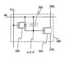
도 1에는, 반도체 장치의 회로 구성의 일례를 나타낸다. 이 반도체 장치는, 산화물 반도체 이외의 재료를 이용한 트랜지스터(160)와 산화물 반도체를 이용한 트랜지스터(162)에 의해 구성된다. 또한, 도 1에서, 트랜지스터(162)는 산화물 반도체(Oxide Semiconductor)를 이용한 것을 명시하기 위해, OS의 부호를 함께 붙이고 있다. 이하의 실시형태에 대해서도 마찬가지이다.Fig. 1 shows an example of a circuit configuration of a semiconductor device. This semiconductor device is constituted by a
여기서, 트랜지스터(160)의 게이트 전극과, 트랜지스터(162)의 소스 전극 또는 드레인 전극의 한쪽은 전기적으로 접속되어 있다. 또한, 제 1 배선(1st Line:소스선(SL)이라고도 부름)과 트랜지스터(160)의 소스 전극은 전기적으로 접속되고, 제 2 배선(2nd Line:비트선(BL)이라고도 부름)과 트랜지스터(160)의 드레인 전극은 전기적으로 접속되어 있다. 그리고, 제 3 배선(3rd Line:제 1 신호선(S1)이라고도 부름)과 트랜지스터(162)의 소스 전극 또는 드레인 전극의 다른 한쪽은 전기적으로 접속되고, 제 4 배선(4th Line:제 2 신호선(S2)이라고도 부름)과 트랜지스터(162)의 게이트 전극은 전기적으로 접속되어 있다.Here, the gate electrode of the
산화물 반도체 이외의 재료를 이용한 트랜지스터(160)는 산화물 반도체를 이용한 트랜지스터와 비교하여, 더욱 고속 동작이 가능하기 때문에, 이것을 이용함으로써, 기억 내용의 판독 등을 고속으로 행하는 것이 가능하다. 또한, 산화물 반도체를 이용한 트랜지스터(162)는 오프 전류가 매우 작다는 특징을 가지고 있다. 이 때문에, 트랜지스터(162)를 오프 상태로 함으로써, 트랜지스터(160)의 게이트 전극의 전위를 매우 장시간에 걸쳐 보유하는 것이 가능하다. 또한, 산화물 반도체를 이용한 트랜지스터(162)에서는 단채널 효과가 나타나기 어렵다는 메리트도 있다.Since the
게이트 전극의 전위를 장시간에 걸쳐 보유할 수 있다는 특징을 살림으로써, 다음과 같이, 정보의 기입, 보유, 판독이 가능하다.By storing the potential of the gate electrode over a long period of time, it is possible to write, hold, and read information as follows.
먼저, 정보의 기입 및 보유에 대하여 설명한다. 우선, 제 4 배선의 전위를, 트랜지스터(162)가 온 상태가 되는 전위로 하여 트랜지스터(162)를 온 상태로 한다. 이것에 의해, 제 3 배선의 전위가 트랜지스터(160)의 게이트 전극에 부여할 수 있다(기입). 그 후, 제 4 배선의 전위를, 트랜지스터(162)가 오프 상태가 되는 전위로 하여 트랜지스터(162)를 오프 상태로 함으로써, 트랜지스터(160)의 게이트 전극의 전위가 보유된다(보유).First, the writing and holding of information will be described. First, the potential of the fourth wiring is set to the potential at which the
트랜지스터(162)의 오프 전류는 매우 작기 때문에, 트랜지스터(160)의 게이트 전극의 전위는 장시간에 걸쳐 보유된다. 예를 들면, 트랜지스터(160)의 게이트 전극의 전위가 트랜지스터(160)를 온 상태로 하는 전위이면, 트랜지스터(160)의 온 상태가 장시간에 걸쳐 보유되게 된다. 또한, 트랜지스터(160)의 게이트 전극의 전위가 트랜지스터(160)를 오프 상태로 하는 전위라면, 트랜지스터(160)의 오프 상태가 장시간에 걸쳐 보유된다.Since the off current of the
다음에, 정보의 판독에 대하여 설명한다. 상술한 바와 같이, 트랜지스터(160)의 온 상태 또는 오프 상태가 보유된 상태에서, 제 1 배선에 소정의 전위(저전위)가 부여되면, 트랜지스터(160)의 온 상태 또는 오프 상태에 따라, 제 2 배선의 전위는 다른 값을 취한다. 예를 들면, 트랜지스터(160)가 온 상태인 경우에는, 제 1 배선의 전위의 영향을 받아, 제 2 배선의 전위가 저하하게 된다. 반대로, 트랜지스터(160)가 오프 상태인 경우에는, 제 2 배선의 전위는 변화하지 않는다.Next, the reading of information will be described. As described above, when a predetermined potential (low potential) is applied to the first wiring in the ON state or OFF state of the
이와 같이, 정보가 보유된 상태에서, 제 2 배선의 전위를 소정의 전위와 비교함으로써, 정보를 읽어낼 수 있다.Thus, in a state in which information is held, information can be read by comparing the potential of the second wiring with a predetermined potential.
다음에, 정보의 다시쓰기에 대하여 설명한다. 정보의 다시쓰기는 상기 정보의 기입 및 보유와 마찬가지로 행해진다. 즉, 제 4 배선의 전위를, 트랜지스터(162)가 온 상태가 되는 전위로 하여 트랜지스터(162)를 온 상태로 한다. 이것에 의해, 제 3 배선의 전위(새로운 정보에 관한 전위)가 트랜지스터(160)의 게이트 전극에 부여된다. 그 후, 제 4 배선의 전위를, 트랜지스터(162)가 오프 상태가 되는 전위로 하여 트랜지스터(162)를 오프 상태로 함으로써, 새로운 정보가 보유된 상태가 된다.Next, rewriting of information will be described. The rewriting of the information is performed in the same manner as the writing and holding of the information. That is, the potential of the fourth wiring is set to the potential at which the
이와 같이, 개시하는 발명에 관한 반도체 장치는 재차의 정보의 기입에 의해 직접적으로 정보를 다시쓰는 것이 가능하다. 따라서 플래시 메모리 등에서 필요한 소거 동작이 불필요하고, 소거 동작에 기인하는 동작 속도의 저하를 억제할 수 있다. 즉, 반도체 장치의 고속 동작이 실현된다.As described above, the semiconductor device according to the disclosed invention can directly rewrite information by rewriting the information. Therefore, a necessary erase operation is not required in the flash memory or the like, and a decrease in the operation speed due to the erase operation can be suppressed. That is, a high-speed operation of the semiconductor device is realized.
또한, 상기 설명은 전자를 캐리어로 하는 n형 트랜지스터(n 채널형 트랜지스터)를 이용하는 경우에 대한 것이지만, n형 트랜지스터 대신에, 정공을 캐리어로 하는 p형 트랜지스터를 이용할 수 있는 것은 말할 필요도 없다.The above description is for the case of using an n-type transistor (n-channel transistor) having electrons as a carrier, but it goes without saying that a p-type transistor having holes as carriers can be used instead of the n-type transistors.
또한, 트랜지스터(160)의 게이트 전극의 전위의 보유를 용이하게 하기 위해, 트랜지스터(160)의 게이트 전극에, 용량 소자 등을 부가해도 좋다는 것은 말할 필요도 없다.Needless to say, a capacitor or the like may be added to the gate electrode of the
<반도체 장치의 평면 구성 및 단면 구성><Planar Configuration and Sectional Configuration of Semiconductor Device>
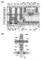
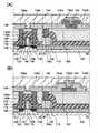
도 2는 상기 반도체 장치의 구성의 일례이다. 도 2(A)에는 반도체 장치의 단면도를, 도 2(B)에는 반도체 장치의 평면도를, 각각 나타낸다. 여기서, 도 2(A)는 도 2(B)의 선 A1-A2 및 선 B1-B2에서의 단면에 상당한다. 도 2(A) 및 도 2(B)에 나타내는 반도체 장치는 하부에 산화물 반도체 이외의 재료를 이용한 트랜지스터(160)를 가지고, 상부에 산화물 반도체를 이용한 트랜지스터(162)를 가지는 것이다. 또한, 트랜지스터(160) 및 트랜지스터(162)는 모두 n형 트랜지스터로서 설명하지만, p형 트랜지스터를 채용해도 좋다. 특히, 트랜지스터(160)는 p형으로 하는 것이 용이하다.2 is an example of the configuration of the semiconductor device. Fig. 2 (A) shows a cross-sectional view of the semiconductor device, and Fig. 2 (B) shows a plan view of the semiconductor device. Here, Fig. 2A corresponds to a cross section taken along line A1-A2 and line B1-B2 in Fig. 2B. The semiconductor device shown in Figs. 2A and 2B has a
트랜지스터(160)는 반도체 재료를 포함하는 기판(100)에 형성된 채널 형성 영역(116)과, 채널 형성 영역(116)을 끼우도록 형성된 불순물 영역(114) 및 고농도 불순물 영역(120)(이것들을 아울러 간단히 불순물 영역이라고도 부름)과, 채널 형성 영역(116) 위에 형성된 게이트 절연층(108)과, 게이트 절연층(108) 위에 형성된 게이트 전극(110)과, 불순물 영역(114)과 전기적으로 접속하는 소스 전극 또는 드레인 전극(130a), 소스 전극 또는 드레인 전극(130b)을 가진다.The
여기서, 게이트 전극(110)의 측면에는 사이드 월 절연층(118)이 형성되어 있다. 또한, 기판(100)의 평면도로 볼 때 사이드 월 절연층(118)과 중첩되지 않는 영역에는 고농도 불순물 영역(120)을 가지고, 고농도 불순물 영역(120) 위에는 금속 화합물 영역(124)이 존재한다. 또한, 기판(100) 위에는 트랜지스터(160)를 둘러싸도록 소자 분리 절연층(106)이 형성되어 있고, 트랜지스터(160)를 덮도록, 층간 절연층(126) 및 층간 절연층(128)이 형성되어 있다. 소스 전극 또는 드레인 전극(130a), 소스 전극 또는 드레인 전극(130b)은 층간 절연층(126) 및 층간 절연층(128)에 형성된 개구를 통하여, 금속 화합물 영역(124)과 전기적으로 접속되어 있다. 즉, 소스 전극 또는 드레인 전극(130a), 소스 전극 또는 드레인 전극(130b)은 금속 화합물 영역(124)을 통하여 고농도 불순물 영역(120) 및 불순물 영역(114)과 전기적으로 접속되어 있다. 또한, 게이트 전극(110)에는, 소스 전극 또는 드레인 전극(130a)이나 소스 전극 또는 드레인 전극(130b)과 마찬가지로 형성된 전극(130c)이 전기적으로 접속되어 있다.A
트랜지스터(162)는 층간 절연층(128) 위에 형성된 게이트 전극(136d)과, 게이트 전극(136d) 위에 형성된 게이트 절연층(138)과, 게이트 절연층(138) 위에 형성된 산화물 반도체층(140)과, 산화물 반도체층(140) 위에 형성되고, 산화물 반도체층(140)과 전기적으로 접속되어 있는 소스 전극 또는 드레인 전극(142a), 소스 전극 또는 드레인 전극(142b)을 가진다.The
여기서, 게이트 전극(136d)은 층간 절연층(128) 위에 형성된 절연층(132)에 파묻히도록 형성되어 있다. 또한, 게이트 전극(136d)과 마찬가지로, 소스 전극 또는 드레인 전극(130a)에 접하여 전극(136a)이, 소스 전극 또는 드레인 전극(130b)에 접하여 전극(136b)이, 전극(130c)에 접하여 전극(136c)이, 각각 형성되어 있다.Here, the
또한, 트랜지스터(162)의 위에는 산화물 반도체층(140)의 일부와 접하도록, 보호 절연층(144)이 형성되어 있고, 보호 절연층(144) 위에는 층간 절연층(146)이 형성되어 있다. 여기서, 보호 절연층(144) 및 층간 절연층(146)에는 소스 전극 또는 드레인 전극(142a), 소스 전극 또는 드레인 전극(142b)에까지 달하는 개구가 형성되어 있고, 이 개구를 통하여, 전극(150d), 전극(150e)이 소스 전극 또는 드레인 전극(142a), 소스 전극 또는 드레인 전극(142b)에 접하여 형성되어 있다. 또한, 전극(150d), 전극(150e)과 마찬가지로, 게이트 절연층(138), 보호 절연층(144), 층간 절연층(146)에 형성된 개구를 통하여, 전극(136a), 전극(136b), 전극(136c)에 접하는 전극(150a), 전극(150b), 전극(150c)이 형성되어 있다.A protective insulating
여기서, 산화물 반도체층(140)은 수소 등의 불순물이 충분히 제거되어, 고순도화되어 있는 것인 것이 바람직하다. 구체적으로는, 산화물 반도체층(140)의 수소 농도는 5×10¹⁹ atoms/cm3 이하, 바람직하게는 5×10¹⁸ atoms/cm3 이하, 보다 바람직하게는 5×10¹⁷ atoms/cm3 이하로 한다. 또한, 충분한 산소를 함유함으로써, 산소 결핍에 기인하는 결함이 저감된 것인 것이 바람직하다. 수소 농도가 충분히 저감되어 고순도화되고, 산소 결핍에 기인하는 결함이 저감된 산화물 반도체층(140)에서는 캐리어 농도가 1×10¹²/cm3 이하, 바람직하게는, 1×10¹¹/cm3 이하가 된다. 이와 같이, i형화 또는 실질적으로 i형화된 산화물 반도체를 이용함으로써, 매우 뛰어난 오프 전류 특성의 트랜지스터(162)를 얻을 수 있다. 예를 들면, 드레인 전압(Vd)이 +1 V 또는 +10 V의 경우이며, 게이트 전압(Vg)이 -5 V에서 -20 V의 범위에서는, 오프 전류는 1×10-13 A 이하이다. 이와 같이, 수소 농도가 충분히 저감되어 고순도화되고, 산소 결핍에 기인하는 결함이 저감된 산화물 반도체층(140)을 적용하여, 트랜지스터(162)의 오프 전류를 저감함으로써, 새로운 구성의 반도체 장치를 실현할 수 있다. 또한, 상술한 산화물 반도체층(140) 중의 수소 농도는 2차 이온 질량 분석법(SIMS:Secondary Ion Mass Spectroscopy)으로 측정한 것이다.Here, it is preferable that the
또한, 층간 절연층(146) 위에는 절연층(152)이 형성되어 있고, 이 절연층(152)에 파묻히도록, 전극(154a), 전극(154b), 전극(154c), 전극(154d)이 형성되어 있다. 여기서, 전극(154a)은 전극(150a)과 접하고 있고, 전극(154b)은 전극(150b)과 접하고 있고, 전극(154c)은 전극(150c) 및 전극(150d)과 접하고 있고, 전극(154d)은 전극(150e)과 접하고 있다.An
즉, 도 2에 나타낸 반도체 장치에서는, 트랜지스터(160)의 게이트 전극(110)과, 트랜지스터(162)의 소스 전극 또는 드레인 전극(142a)이 전극(130c), 전극(136c), 전극(150c), 전극(154c) 및 전극(150d)을 통하여 전기적으로 접속되어 있다.2, the
<반도체 장치의 제작 방법><Manufacturing Method of Semiconductor Device>
다음에, 상기 반도체 장치의 제작 방법의 일례에 대하여 설명한다. 이하에서는, 처음에 하부의 트랜지스터(160)의 제작 방법에 대하여 도 3을 참조하여 설명하고, 그 후, 상부의 트랜지스터(162)의 제작 방법에 대하여 도 4 및 도 5를 참조하여 설명한다.Next, an example of a manufacturing method of the semiconductor device will be described. Hereinafter, a method of manufacturing the
<하부의 트랜지스터의 제작 방법>≪ Method of fabricating lower transistor &
먼저, 반도체 재료를 포함하는 기판(100)을 준비한다(도 3(A) 참조). 반도체 재료를 포함하는 기판(100)으로서는, 실리콘이나 탄화 실리콘 등의 단결정 반도체 기판, 다결정 반도체 기판, 실리콘 게르마늄 등의 화합물 반도체 기판, SOI 기판 등을 적용할 수 있다. 여기에서는, 반도체 재료를 포함하는 기판(100)으로서, 단결정 실리콘 기판을 이용하는 경우의 일례에 대하여 나타내는 것으로 한다.First, a
기판(100) 위에는, 소자 분리 절연층을 형성하기 위한 마스크가 되는 보호층(102)을 형성한다(도 3(A) 참조). 보호층(102)으로서는, 예를 들면, 산화실리콘이나 질화실리콘, 질화산화실리콘 등을 재료로 하는 절연층을 이용할 수 있다. 또한, 이 공정의 전후에, 트랜지스터의 스레숄드 전압을 제어하기 위해, n형의 도전성을 부여하는 불순물 원소나 p형의 도전성을 부여하는 불순물 원소를 기판(100)에 첨가해도 좋다. 반도체가 실리콘인 경우, n형의 도전성을 부여하는 불순물로서는, 예를 들면, 인이나 비소 등을 이용할 수 있다. 또한, p형의 도전성을 부여하는 불순물로서는, 예를 들면, 붕소, 알루미늄, 갈륨 등을 이용할 수 있다.On the
다음에, 상기의 보호층(102)을 마스크로서 에칭을 행하고, 보호층(102)에 덮여지지 않은 영역(노출되어 있는 영역)의 기판(100)의 일부를 제거한다. 이것에 의해 분리된 반도체 영역(104)이 형성된다(도 3(B) 참조). 이 에칭에는 드라이 에칭을 이용하는 것이 적합하지만, 웨트 에칭을 이용해도 좋다. 에칭 가스나 에칭액에 대해서는 피에칭 재료에 따라 적절히 선택할 수 있다.Next, etching is performed using the above-described
다음에, 반도체 영역(104)을 덮도록 절연층을 형성하여, 반도체 영역(104)에 중첩하는 영역의 절연층을 선택적으로 제거함으로써, 소자 분리 절연층(106)을 형성한다(도 3(B) 참조). 이 절연층은 산화실리콘이나 질화실리콘, 질화산화실리콘 등을 이용하여 형성된다. 절연층의 제거 방법으로서는, CMP 등의 연마 처리나 에칭 처리 등이 있지만, 그 중 어느 것인가를 이용해도 좋다. 또한, 반도체 영역(104)의 형성 후, 또는, 소자 분리 절연층(106)의 형성 후에는 상기 보호층(102)을 제거한다.Next, an insulating layer is formed so as to cover the
다음에, 반도체 영역(104) 위에 절연층을 형성하고, 이 절연층 위에 도전 재료를 포함하는 층을 형성한다.Next, an insulating layer is formed on the
절연층은 후의 게이트 절연층이 되는 것이고, CVD법이나 스퍼터링법 등을 이용하여 얻어지는 산화실리콘, 질화산화실리콘, 질화실리콘, 산화하프늄, 산화알루미늄, 산화탄탈 등을 포함하는 막의 단층 구조 또는 적층 구조로 하면 좋다. 그 외에, 고밀도 플라즈마 처리나 열산화처리에 의해, 반도체 영역(104)의 표면을 산화, 질화시킴으로써, 상기 절연층을 형성해도 좋다. 고밀도 플라즈마 처리는, 예를 들면, He, Ar, Kr, Xe 등의 희가스와, 산소, 산화질소, 암모니아, 질소, 수소 등의 혼합 가스를 이용하여 행할 수 있다. 또한, 절연층의 두께는 특별히 한정되지 않지만, 예를 들면, 1 nm 이상 100 nm 이하로 할 수 있다.The insulating layer serves as a later gate insulating layer and may be a single layer structure or a laminated structure of a film containing silicon oxide, silicon nitride oxide, silicon nitride, hafnium oxide, aluminum oxide, tantalum oxide, or the like obtained by a CVD method or a sputtering method It is good. In addition, the insulating layer may be formed by oxidizing and nitriding the surface of the
도전 재료를 포함하는 층은 알루미늄이나 구리, 티탄, 탄탈, 텅스텐 등의 금속 재료를 이용하여 형성할 수 있다. 또한, 도전 재료를 포함하는 다결정 실리콘 등의 반도체 재료를 이용하여, 도전 재료를 포함하는 층을 형성해도 좋다. 형성 방법도 특별히 한정되지 않고, 증착법, CVD법, 스퍼터링법, 스핀 코트법 등의 각종 성막 방법을 이용할 수 있다. 또한, 본 실시형태에서는 금속 재료를 이용하여 도전 재료를 포함하는 층을 형성하는 경우의 일례에 대하여 나타내는 것으로 한다.The layer containing the conductive material can be formed using a metal material such as aluminum, copper, titanium, tantalum, or tungsten. Further, a layer containing a conductive material may be formed using a semiconductor material such as polycrystalline silicon containing a conductive material. The forming method is not particularly limited, and various film forming methods such as a vapor deposition method, a CVD method, a sputtering method, and a spin coating method can be used. In this embodiment, a layer including a conductive material is formed using a metal material.
그 후, 절연층 및 도전 재료를 포함하는 층을 선택적으로 에칭하여, 게이트 절연층(108), 게이트 전극(110)을 형성한다(도 3(C) 참조).Thereafter, the insulating layer and the layer including the conductive material are selectively etched to form the
다음에, 게이트 전극(110)을 덮는 절연층(112)을 형성한다(도 3(C) 참조). 그리고, 반도체 영역(104)에 인(P)이나 비소(As) 등을 첨가하여, 기판(100)과의 얕은 접합 깊이의 불순물 영역(114)을 형성한다(도 3(C) 참조). 또한, 여기에서는 n형 트랜지스터를 형성하기 위해 인이나 비소를 첨가하고 있지만, p형 트랜지스터를 형성하는 경우에는, 붕소(B)나 알루미늄(Al) 등의 불순물 원소를 첨가하면 좋다. 또한, 불순물 영역(114)의 형성에 의해, 반도체 영역(104)의 게이트 절연층(108) 하부에는, 채널 형성 영역(116)이 형성된다(도 3(C) 참조). 여기서, 첨가하는 불순물의 농도는 적절히 설정할 수 있지만, 반도체 소자가 고도로 미세화되는 경우에는, 그 농도를 높게 하는 것이 바람직하다. 또한, 여기에서는, 절연층(112)을 형성한 후에 불순물 영역(114)을 형성하는 공정을 채용하고 있지만, 불순물 영역(114)을 형성한 후에 절연층(112)을 형성하는 공정으로 해도 좋다.Next, an insulating
다음에, 사이드 월 절연층(118)을 형성한다(도 3(D) 참조). 사이드 월 절연층(118)은 절연층(112)을 덮도록 절연층을 형성한 후에, 이 절연층에 이방성이 높은 에칭 처리를 적용함으로써, 자기 정합적으로 형성할 수 있다. 또한, 이때에, 절연층(112)을 부분적으로 에칭하여, 게이트 전극(110)의 상면과, 불순물 영역(114)의 상면을 노출시키면 좋다.Next, a
다음에, 게이트 전극(110), 불순물 영역(114), 사이드 월 절연층(118) 등을 덮도록, 절연층을 형성한다. 그리고, 이 절연층이 불순물 영역(114)과 접하는 영역에, 인(P)이나 비소(As) 등을 첨가하여, 고농도 불순물 영역(120)을 형성한다(도 3(E) 참조). 그 후, 상기 절연층을 제거하여, 게이트 전극(110), 사이드 월 절연층(118), 고농도 불순물 영역(120) 등을 덮도록 금속층(122)을 형성한다(도 3(E) 참조). 이 금속층(122)은 진공 증착법이나 스퍼터링법, 스핀 코트법 등의 각종 성막 방법을 이용하여 형성할 수 있다. 금속층(122)은 반도체 영역(104)을 구성하는 반도체 재료와 반응하여 저저항인 금속 화합물이 되는 금속 재료를 이용하여 형성하는 것이 바람직하다. 이러한 금속 재료로서는, 예를 들면, 티탄, 탄탈, 텅스텐, 니켈, 코발트, 백금 등이 있다.Next, an insulating layer is formed so as to cover the
다음에, 열처리를 실시하여, 상기 금속층(122)과 반도체 재료를 반응시킨다. 이것에 의해, 고농도 불순물 영역(120)에 접하는 금속 화합물 영역(124)이 형성된다(도 3(F) 참조). 또한, 게이트 전극(110)으로서 다결정 실리콘 등을 이용하는 경우에는, 게이트 전극(110)의 금속층(122)과 접촉하는 부분에도, 금속 화합물 영역이 형성되게 된다.Next, a heat treatment is performed to cause the
상기 열처리로서는, 예를 들면, 플래시 램프의 조사에 의한 열처리를 이용할 수 있다. 물론, 그 외의 열처리 방법을 이용해도 좋지만, 금속 화합물의 형성에 관한 화학 반응의 제어성을 향상시키기 위해서는, 매우 단시간의 열처리를 실현될 수 있는 방법을 이용하는 것이 바람직하다. 또한, 상기의 금속 화합물 영역은 금속 재료와 반도체 재료와의 반응에 의해 형성되는 것이고, 충분히 도전성이 높아진 영역이다. 이 금속 화합물 영역을 형성함으로써, 전기 저항을 충분히 저감하여, 소자 특성을 향상시킬 수 있다. 또한, 금속 화합물 영역(124)을 형성한 후에는, 금속층(122)은 제거한다.As the heat treatment, for example, heat treatment by irradiation with a flash lamp can be used. Of course, other heat treatment methods may be used. However, in order to improve the controllability of the chemical reaction relating to the formation of the metal compound, it is preferable to employ a method capable of realizing a very short time heat treatment. Further, the above-described metal compound region is formed by the reaction of the metal material and the semiconductor material, and is a region where the conductivity is sufficiently increased. By forming this metal compound region, it is possible to sufficiently reduce the electrical resistance and improve the device characteristics. Further, after the
다음에, 상술한 공정에 의해 형성된 각 구성을 덮도록, 층간 절연층(126), 층간 절연층(128)을 형성한다(도 3(G) 참조). 층간 절연층(126)이나 층간 절연층(128)은 산화실리콘, 질화산화실리콘, 질화실리콘, 산화하프늄, 산화알루미늄, 산화탄탈 등의 무기 절연 재료를 포함하는 재료를 이용하여 형성할 수 있다. 또한, 폴리이미드, 아크릴 등의 유기 절연 재료를 이용하여 형성하는 것도 가능하다. 또한, 여기에서는, 층간 절연층(126)과 층간 절연층(128)의 2층 구조로 하고 있지만, 층간 절연층의 구성은 이것에 한정되지 않는다. 층간 절연층(128)의 형성 후에는, 그 표면을 CMP나 에칭 처리 등에 의해 평탄화해 두는 것이 바람직하다.Next, an
그 후, 상기 층간 절연층에, 금속 화합물 영역(124)에까지 달하는 개구를 형성하고, 이 개구에 소스 전극 또는 드레인 전극(130a), 소스 전극 또는 드레인 전극(130b)을 형성한다(도 3(H) 참조). 소스 전극 또는 드레인 전극(130a)이나 소스 전극 또는 드레인 전극(130b)은, 예를 들면, 개구를 포함하는 영역에 PVD법이나 CVD법 등을 이용하여 도전층을 형성한 후, 에칭 처리나 CMP와 같은 방법을 이용하여, 상기 도전층의 일부를 제거함으로써 형성할 수 있다.Thereafter, an opening reaching the
또한, 상기 도전층의 일부를 제거하여 소스 전극 또는 드레인 전극(130a)이나 소스 전극 또는 드레인 전극(130b)을 형성할 때에는, 그 표면이 평탄하게 되도록 가공하는 것이 바람직하다. 예를 들면, 개구를 포함하는 영역에 티탄막이나 질화티탄막을 얇게 형성한 후에, 개구에 묻도록 텅스텐막을 형성하는 경우에는 그 후의 CMP에 의해, 불필요한 텅스텐막, 티탄막, 질화티탄막 등을 제거함과 동시에, 그 표면의 평탄성을 향상시킬 수 있다. 이와 같이, 소스 전극 또는 드레인 전극(130a), 소스 전극 또는 드레인 전극(130b)을 포함하는 표면을 평탄화함으로써, 후의 공정에서, 양호한 전극, 배선, 절연층, 반도체층 등을 형성하는 것이 가능하게 된다.When the source electrode or the
또한, 여기에서는, 금속 화합물 영역(124)과 접촉하는 소스 전극 또는 드레인 전극(130a)이나 소스 전극 또는 드레인 전극(130b)만을 나타내고 있지만, 이 공정에서, 게이트 전극(110)과 접촉하는 전극(예를 들면, 도 2(A)에서의 전극(130c)) 등을 아울러 형성할 수 있다. 소스 전극 또는 드레인 전극(130a), 소스 전극 또는 드레인 전극(130b)으로서 이용할 수 있는 재료에 대하여 특별히 한정은 없고, 각종 도전 재료를 이용할 수 있다. 예를 들면, 몰리브덴, 티탄, 크롬, 탄탈, 텅스텐, 알루미늄, 구리, 네오디뮴, 스칸듐 등의 도전성 재료를 이용할 수 있다.Here, only the source electrode or the
이상에 의해, 반도체 재료를 포함하는 기판(100)을 이용한 트랜지스터(160)가 형성된다. 또한, 상기 공정의 후에는, 전극이나 배선, 절연층 등을 더 형성해도 좋다. 배선의 구조로서 층간 절연층 및 도전층의 적층 구조로 이루어지는 다층 배선 구조를 채용함으로써, 고도로 집적화된 반도체 장치를 제공할 수 있다.Thus, the
<상부의 트랜지스터의 제작 방법>≪ Manufacturing method of upper transistor >
다음에, 도 4 및 도 5를 이용하여, 층간 절연층(128) 위에 트랜지스터(162)를 제작하는 공정에 대하여 설명한다. 또한, 도 4 및 도 5는 층간 절연층(128) 위의 각종 전극이나, 트랜지스터(162) 등의 제작 공정을 나타내는 것이기 때문에, 트랜지스터(162)의 하부에 존재하는 트랜지스터(160) 등에 대해서는 생략하고 있다.Next, a process of manufacturing the
먼저, 층간 절연층(128), 소스 전극 또는 드레인 전극(130a), 소스 전극 또는 드레인 전극(130b), 전극(130c) 위에 절연층(132)을 형성한다(도 4(A) 참조). 절연층(132)은 PVD법이나 CVD법 등을 이용하여 형성할 수 있다. 또한, 산화실리콘, 질화산화실리콘, 질화실리콘, 산화하프늄, 산화알루미늄, 산화탄탈 등의 무기 절연 재료를 포함하는 재료를 이용하여 형성할 수 있다.First, an insulating
다음에, 절연층(132)에 대하여, 소스 전극 또는 드레인 전극(130a), 소스 전극 또는 드레인 전극(130b), 및 전극(130c)에까지 달하는 개구를 형성한다. 이 때, 후에 게이트 전극(136d)이 형성되는 영역에도 아울러 개구를 형성한다. 그리고, 상기 개구에 묻도록, 도전층(134)을 형성한다(도 4(B) 참조). 상기 개구는 마스크를 이용한 에칭 등의 방법으로 형성할 수 있다. 이 마스크는 포토마스크를 이용한 노광 등의 방법에 의해 형성하는 것이 가능하다. 에칭으로서는 웨트 에칭, 드라이 에칭의 어느 것을 이용해도 좋지만, 미세 가공의 관점에서는 드라이 에칭을 이용하는 것이 적합하다. 도전층(134)의 형성은 PVD법이나 CVD법 등의 성막법을 이용하여 행할 수 있다. 도전층(134)의 형성에 이용할 수 있는 재료로서는, 몰리브덴, 티탄, 크롬, 탄탈, 텅스텐, 알루미늄, 구리, 네오디뮴, 스칸듐 등의 도전성 재료나, 이들의 합금, 화합물(예를 들면 질화물) 등을 들 수 있다.Next, an opening reaching the source electrode or the
보다 구체적으로, 도전층(134)은 다음과 같이 형성될 수 있는데, 예를 들면 개구를 포함하는 영역에 PVD법에 의해 티탄막을 얇게 형성하고, CVD법에 의해 질화티탄막을 얇게 형성한 후에, 개구에 묻도록 텅스텐막을 형성하는 방법을 적용할 수 있다. 여기서, PVD법에 의해 형성되는 티탄막은 하부 전극(여기에서는 소스 전극 또는 드레인 전극(130a), 소스 전극 또는 드레인 전극(130b), 전극(130c) 등)과의 계면의 산화막을 환원하여, 하부 전극과의 접촉 저항을 저감시키는 기능을 가진다. 또한, 그 후에 형성되는 질화티탄막은 도전성 재료의 확산을 억제하는 배리어 기능을 구비한다. 또한, 티탄이나, 질화티탄 등에 의한 배리어막을 형성한 후에, 도금법에 의해 구리막을 형성해도 좋다.More specifically, the
도전층(134)을 형성한 후에는, 에칭 처리나 CMP와 같은 방법을 이용하여 도전층(134)의 일부를 제거하고, 절연층(132)을 노출시켜, 전극(136a), 전극(136b), 전극(136c), 게이트 전극(136d)을 형성한다(도 4(C) 참조). 또한, 상기 도전층(134)의 일부를 제거하여 전극(136a), 전극(136b), 전극(136c), 게이트 전극(136d)을 형성할 때에는, 표면이 평탄하게 되도록 가공하는 것이 바람직하다. 이와 같이, 절연층(132), 전극(136a), 전극(136b), 전극(136c), 게이트 전극(136d)의 표면을 평탄화함으로써, 후의 공정에서, 양호한 전극, 배선, 절연층, 반도체층 등을 형성하는 것이 가능하게 된다.After the
다음에, 절연층(132), 전극(136a), 전극(136b), 전극(136c), 게이트 전극(136d)을 덮도록, 게이트 절연층(138)을 형성한다(도 4(D) 참조). 게이트 절연층(138)은 CVD법이나 스퍼터링법 등을 이용하여 형성할 수 있다. 또한, 게이트 절연층(138)은, 산화규소, 질화규소, 산화질화규소, 질화산화규소, 산화알루미늄, 산화하프늄, 산화탄탈 등을 포함하도록 형성하는 것이 적합하다. 또한, 게이트 절연층(138)은 단층 구조로 해도 좋고, 적층 구조로 해도 좋다. 예를 들면, 원료 가스로서 실란(SiH4), 산소, 질소를 이용한 플라즈마 CVD법에 의해, 산화질화규소로 이루어지는 게이트 절연층(138)을 형성할 수 있다. 게이트 절연층(138)의 두께는 특별히 한정되지 않지만, 예를 들면, 10 nm 이상 500 nm 이하로 할 수 있다. 적층 구조의 경우는, 예를 들면, 막두께 50 nm 이상 200 nm 이하의 제 1 게이트 절연층과, 제 1 게이트 절연층 위의 막두께 5 nm 이상 300 nm 이하의 제 2 게이트 절연층의 적층으로 하면 적합하다.Next, a
또한, 불순물을 제거함으로써 i형화 또는 실질적으로 i형화된 산화물 반도체(고순도화된 산화물 반도체)는, 계면 준위나 계면 전하에 대하여 매우 민감하기 때문에, 이러한 산화물 반도체를 산화물 반도체층에 이용하는 경우에는, 게이트 절연층과의 계면은 중요하다. 즉, 고순도화된 산화물 반도체층에 접하는 게이트 절연층(138)에는 고품질화가 요구되게 된다.Further, since the oxide semiconductor (highly purified oxide semiconductors) that is i-type or substantially i-shaped by removing the impurities is very sensitive to the interface level and the interface charge, when such an oxide semiconductor is used for the oxide semiconductor layer, The interface with the insulating layer is important. That is, the quality of the
예를 들면, μ파(2.45 GHz)를 이용한 고밀도 플라즈마 CVD법은 치밀하고 절연 내압이 높은 고품질의 게이트 절연층(138)을 형성할 수 있다는 점에서 적합하다. 고순도화된 산화물 반도체층과 고품질 게이트 절연층이 접촉함으로써, 계면 준위를 저감하여 계면 특성을 양호한 것으로 할 수 있기 때문이다.For example, the high-density plasma CVD method using a microwave (2.45 GHz) is suitable in that it can form a high-quality
물론, 게이트 절연층으로서 양질의 절연층을 형성할 수 있는 것이라면, 고순도화된 산화물 반도체층을 이용하는 경우에도, 스퍼터링법이나 플라즈마 CVD법 등 다른 방법을 적용할 수 있다. 또한, 형성 후의 열처리에 의해, 막질이나 산화물 반도체층과의 계면 특성이 개질되는 절연층을 적용해도 좋다. 어쨌든, 게이트 절연층(138)으로서의 막질이 양호함과 동시에, 산화물 반도체층과의 계면 준위 밀도를 저감하여, 양호한 계면을 형성할 수 있는 것을 형성하면 좋다.Of course, if a high-quality insulating layer can be formed as a gate insulating layer, another method such as sputtering or plasma CVD can be applied even when a high-purity oxide semiconductor layer is used. An insulating layer may be used in which the interface property with the film quality or the oxide semiconductor layer is modified by heat treatment after formation. In any case, it is preferable that the film quality as the
또한, 온도 85℃, 전계 강도 2×10⁶ V/cm, 12시간의 게이트 바이어스·열스트레스 시험(BT 시험)에서는, 불순물이 산화물 반도체에 첨가되어 있으면, 불순물과 산화물 반도체의 주성분과의 결합이, 강전계(B:바이어스)와 고온(T:온도)에 의해 절단되어, 생성된 미결합손이 스레숄드 전압(Vth)의 시프트를 유발하게 된다.Further, in the gate bias thermal stress test (BT test) at a temperature of 85 占 폚 and an electric field strength of 2 占06 V / cm for 12 hours, if impurities are added to the oxide semiconductor, the bonding between the impurity and the main component of the oxide semiconductor , The strong electric field (B: bias) and the high temperature (T: temperature), and the generated unbonded hand causes a shift of the threshold voltage Vth.
이것에 대하여, 산화물 반도체의 불순물, 특히 수소나 물 등을 극력 배제하여, 상기와 같이 게이트 절연층과의 계면 특성을 양호하게 함으로써, BT 시험에 대해서도 안정적인 트랜지스터를 얻는 것이 가능하다.On the other hand, it is possible to obtain stable transistors even for the BT test by removing the impurities of the oxide semiconductor, in particular, hydrogen and water, to the extent that the interface characteristics with the gate insulating layer are excellent.
다음에, 게이트 절연층(138) 위에, 산화물 반도체층을 형성하여, 마스크를 이용한 에칭 등의 방법에 의해 이 산화물 반도체층을 가공하여, 섬 형상의 산화물 반도체층(140)을 형성한다(도 4(E) 참조).Next, an oxide semiconductor layer is formed on the
산화물 반도체층으로서는, 4원계 금속 산화물인 In-Sn-Ga-Zn-O나, 3원계 금속 산화물인 In-Ga-Zn-O, In-Sn-Zn-O, In-Al-Zn-O, Sn-Ga-Zn-O, Al-Ga-Zn-O, Sn-Al-Zn-O나, 2원계 금속 산화물인 In-Zn-O, Sn-Zn-O, Al-Zn-O, Zn-Mg-O, Sn-Mg-O, In-Mg-O나, In-O, Sn-O, Zn-O 등을 이용한 산화물 반도체층을 적용할 수 있다. 또한, 상기 산화물 반도체 재료에 SiO2를 포함시켜도 좋다.In-Sn-Zn-O, which is a quaternary metal oxide, In-Ga-Zn-O, In-Sn-Zn-O, Sn-Zn-O, Al-Ga-Zn-O, Sn-Al-Zn-O and binary metal oxides such as In-Zn-O, Sn- An oxide semiconductor layer using Mg-O, Sn-Mg-O, In-Mg-O, In-O, Sn-O and Zn-O can be applied. Further, SiO2 may be included in the oxide semiconductor material.
또한, 산화물 반도체층은 InMO3(ZnO)m(m>0)로 표기되는 박막을 이용할 수 있다. 여기서, M은, Ga, Al, Mn 및 Co로부터 선택된 하나 또는 복수의 금속 원소를 나타낸다. 예를 들면 M으로서 Ga, Ga 및 Al, Ga 및 Mn, 또는 Ga 및 Co 등이 있다. InMO3(ZnO)m(m>0)으로 표기되는 구조의 산화물 반도체막 중, M으로서 Ga를 포함하는 구조의 산화물 반도체를, In-Ga-Zn-O 산화물 반도체라고 부르고, 그 박막을 In-Ga-Zn-O 산화물 반도체막(In-Ga-Zn-O 비정질막) 등이라고 부르기로 한다.The oxide semiconductor layer may be a thin film denoted by InMO3 (ZnO)m (m > 0). Here, M represents one or a plurality of metal elements selected from Ga, Al, Mn and Co. For example, Ga, Ga and Al, Ga and Mn, or Ga and Co as M. Among the oxide semiconductor films having a structure represented by InMO3 (ZnO)m (m > 0), an oxide semiconductor having a structure containing Ga as M is referred to as an In-Ga-Zn-O oxide semiconductor, Ga-Zn-O oxide semiconductor film (In-Ga-Zn-O amorphous film) or the like.
본 실시형태에서는, 산화물 반도체층으로서 In-Ga-Zn-O계의 산화물 반도체 성막용 타겟을 이용하여, 비정질의 산화물 반도체층을 스퍼터링법에 의해 형성하는 것으로 한다. 또한, 비정질의 산화물 반도체층 중에 실리콘을 첨가함으로써, 그 결정화를 억제할 수 있기 때문에, 예를 들면, SiO2를 2 중량% 이상 10 중량% 이하 포함하는 타겟을 이용하여 산화물 반도체층을 형성해도 좋다.In this embodiment mode, an amorphous oxide semiconductor layer is formed by a sputtering method using an In-Ga-Zn-O-based oxide semiconductor film formation target as the oxide semiconductor layer. Further, since the crystallization can be suppressed by adding silicon to the amorphous oxide semiconductor layer, the oxide semiconductor layer may be formed using, for example, a target containing SiO2 in an amount of 2 wt% to 10 wt% .
산화물 반도체층을 스퍼터링법으로 제작하기 위한 타겟으로서는, 예를 들면, 산화아연을 주성분으로 하는 산화물 반도체 성막용 타겟을 이용할 수 있다. 또한, In, Ga, 및 Zn을 포함하는 산화물 반도체 성막용 타겟(조성비로서 In2O3:Ga2O3:ZnO = 1:1:1[mol비]) 등을 이용할 수도 있다. 또한, In, Ga, 및 Zn을 포함하는 산화물 반도체 성막용 타겟으로서 In2O3:Ga2O3:ZnO = 1:1:2[mol비], 또는 In2O3:Ga2O3:ZnO = 1:1:4[mol비]의 조성비를 가지는 타겟 등을 이용해도 좋다. 산화물 반도체 성막용 타겟의 충전율은 90% 이상 100% 이하, 바람직하게는 95% 이상(예를 들면 99.9%)이다. 충전율이 높은 산화물 반도체 성막용 타겟을 이용함으로써, 치밀한 산화물 반도체층이 형성된다.As a target for forming the oxide semiconductor layer by a sputtering method, for example, a target for forming an oxide semiconductor film containing zinc oxide as a main component can be used. In addition, a target for forming an oxide semiconductor film containing In, Ga and Zn (composition ratio In2 O3 : Ga2 O3 : ZnO = 1: 1: 1 [molar ratio]) may be used. In addition, as the target for forming an oxide semiconductor containing In, Ga and Zn, In2 O3 : Ga2 O3 : ZnO = 1: 1: 2 [molar ratio] or In2 O3 : Ga2 O3 : A target having a composition ratio of ZnO = 1: 1: 4 [molar ratio] or the like may be used. The filling rate of the oxide semiconductor film forming target is 90% or more and 100% or less, preferably 95% or more (for example, 99.9%). By using a target for forming an oxide semiconductor film having a high filling rate, a dense oxide semiconductor layer is formed.
산화물 반도체층의 형성 분위기는, 희가스(대표적으로는 아르곤) 분위기, 산소 분위기, 또는, 희가스(대표적으로는 아르곤)와 산소와의 혼합 분위기로 하는 것이 적합하다. 구체적으로는, 예를 들면, 수소, 물, 수산기 또는 수소화물 등의 불순물의 농도가 수 ppm 정도(바람직하게는 수 ppb 정도)까지 제거된 고순도 가스를 이용하는 것이 적합하다.The atmosphere for forming the oxide semiconductor layer is preferably a rare gas (typically argon) atmosphere, an oxygen atmosphere, or a mixed atmosphere of rare gas (typically argon) and oxygen. Specifically, it is preferable to use a high purity gas in which the concentration of impurities such as hydrogen, water, hydroxyl groups, or hydrides is reduced to several ppm (preferably several ppb or so).
산화물 반도체층의 형성 시에는, 감압 상태로 보유된 처리실 내에 기판을 보유하고, 기판 온도를 100℃ 이상 600℃ 이하 바람직하게는 200℃ 이상 400℃ 이하로 한다. 기판을 가열하면서 산화물 반도체층을 형성함으로써, 산화물 반도체층에 포함되는 불순물 농도를 저감할 수 있다. 또한, 스퍼터링에 의한 손상이 경감된다. 그리고, 처리실 내의 잔류 수분을 제거하면서 수소 및 물이 제거된 스퍼터링 가스를 도입하여, 금속 산화물을 타겟으로서 산화물 반도체층을 형성한다. 처리실 내의 잔류 수분을 제거하기 위해서는, 흡착형의 진공 펌프를 이용하는 것이 바람직하다. 예를 들면, 크라이오 펌프, 이온 펌프, 티탄 서블리메이션 펌프를 이용할 수 있다. 또한, 배기 수단으로서는, 터보 펌프에 콜드 트랩을 더한 것이어도 좋다. 크라이오 펌프를 이용하여 배기한 성막실은, 예를 들면, 수소 원자, 물(H2O) 등 수소 원자를 포함하는 화합물(보다 바람직하게는 탄소 원자를 포함하는 화합물도) 등이 배기되기 때문에, 이 성막실에서 형성한 산화물 반도체층에 포함되는 불순물의 농도를 저감할 수 있다.When the oxide semiconductor layer is formed, the substrate is held in a processing chamber held in a reduced pressure state, and the substrate temperature is set to be not less than 100 ° C and not more than 600 ° C, preferably not less than 200 ° C and not more than 400 ° C. By forming the oxide semiconductor layer while heating the substrate, the impurity concentration contained in the oxide semiconductor layer can be reduced. In addition, damage caused by sputtering is reduced. Then, a sputtering gas from which hydrogen and water are removed is introduced while removing residual moisture in the treatment chamber, and an oxide semiconductor layer is formed using the metal oxide as a target. In order to remove the residual moisture in the treatment chamber, it is preferable to use an adsorption type vacuum pump. For example, a cryo pump, an ion pump, and a titanium sublimation pump can be used. As the exhaust means, a cold trap may be added to the turbo pump. Since the film forming chamber exhausted by using the cryo pump is exhausted, for example, a hydrogen atom, a compound containing a hydrogen atom such as water (H2 O) (more preferably a compound containing a carbon atom) The concentration of the impurity contained in the oxide semiconductor layer formed in the deposition chamber can be reduced.
형성 조건으로서는, 예를 들면, 기판과 타겟 사이의 거리가 100 mm, 압력이 0.6 Pa, 직류(DC) 전력이 0.5 kW, 분위기가 산소(산소 유량 비율 100%) 분위기와 같은 조건을 적용할 수 있다. 또한, 펄스 직류(DC) 전원을 이용하면, 성막 시에 발생하는 분상 물질(파티클, 먼지라고도 함)을 경감할 수 있어, 막두께의 편차도 작아지기 때문에 바람직하다. 산화물 반도체층의 두께는 2 nm 이상 200 nm 이하, 바람직하게는 5 nm 이상 30 nm 이하로 한다. 또한, 적용하는 산화물 반도체 재료에 의해 적절한 두께는 다르기 때문에, 그 두께는 이용하는 재료에 따라 적절히 선택하면 좋다.For example, conditions such as a distance between the substrate and the target of 100 mm, a pressure of 0.6 Pa, a direct current (DC) power of 0.5 kW and an atmosphere of oxygen (oxygen flow rate ratio of 100%) can be applied have. In addition, the use of a pulsed direct current (DC) power supply is preferable because it can reduce the amount of dispersed substances (also referred to as particles and dust) generated at the time of film formation, and the variation in the film thickness becomes small. The thickness of the oxide semiconductor layer is 2 nm or more and 200 nm or less, preferably 5 nm or more and 30 nm or less. Since the appropriate thickness varies depending on the oxide semiconductor material to be applied, the thickness may be suitably selected in accordance with the material to be used.
또한, 산화물 반도체층을 스퍼터링법에 의해 형성하기 전에는, 아르곤 가스를 도입하여 플라즈마를 발생시키는 역스퍼터링을 행하여, 게이트 절연층(138)의 표면에 부착되어 있는 먼지를 제거하는 것이 적합하다. 여기서, 역스퍼터링이란, 통상의 스퍼터링에서는, 스퍼터링 타겟으로 이온을 충돌시키지만, 반대로, 처리 표면에 이온을 충돌시키는 것에 의해 그 표면을 개질하는 방법을 말한다. 처리 표면에 이온을 충돌시키는 방법으로서는, 아르곤 분위기하에서 처리 표면측에 고주파 전압을 인가하여, 기판 부근에 플라즈마를 생성하는 방법 등이 있다. 또한, 아르곤 분위기 대신에 질소 분위기, 헬륨 분위기, 산소 분위기 등을 이용해도 좋다.Before the oxide semiconductor layer is formed by the sputtering method, it is preferable to carry out inverse sputtering in which argon gas is introduced to generate plasma to remove dust adhering to the surface of the
상기 산화물 반도체층의 에칭에는, 드라이 에칭, 웨트 에칭의 어느 것을 이용해도 좋다. 물론, 양쪽 모두를 조합하여 이용할 수도 있다. 소망의 형상으로 에칭할 수 있도록, 재료에 맞추어 에칭 조건(에칭 가스나 에칭액, 에칭 시간, 온도 등)을 적절히 설정한다.As the etching of the oxide semiconductor layer, either dry etching or wet etching may be used. Of course, both can be used in combination. The etching conditions (etching gas, etching solution, etching time, temperature, and the like) are appropriately set in accordance with the material so that the desired shape can be etched.
드라이 에칭에 이용하는 에칭 가스에는, 예를 들면, 염소를 포함하는 가스(염소계 가스, 예를 들면 염소(Cl2), 염화붕소(BCl3), 염화규소(SiCl4), 사염화탄소(CCl4) 등) 등이 있다. 또한, 불소를 포함하는 가스(불소계 가스, 예를 들면 사불화탄소(CF4), 불화유황(SF6), 불화질소(NF3), 트리플루오로메탄(CHF3) 등), 브롬화수소(HBr), 산소(O2), 이들 가스에 헬륨(He)이나 아르곤(Ar) 등의 희가스를 첨가한 가스 등을 이용해도 좋다.In the etching gas used for dry etching, for example, a gas including chlorine (chlorine-based gas such as chlorine (Cl2), boron chloride (BCl3), silicon chloride (SiCl4), carbon tetrachloride (CCl4), etc. ). In addition, a gas containing fluorine (fluorine-based gas such as carbon tetrafluoride (CF4 ), sulfur fluoride (SF6 ), nitrogen fluoride (NF3 ), trifluoromethane (CHF3 ) ), Oxygen (O2 ), a gas obtained by adding a rare gas such as helium (He) or argon (Ar) to these gases, or the like may be used.
드라이 에칭법으로서는, 평행 평판형 RIE(Reactive Ion Etching)법이나, ICP(Inductively Coupled Plasma:유도 결합형 플라즈마) 에칭법을 이용할 수 있다. 소망의 형상으로 에칭할 수 있도록, 에칭 조건(코일형의 전극에 인가되는 전력량, 기판측의 전극에 인가되는 전력량, 기판측의 전극 온도 등)은 적절히 설정한다.As the dry etching method, a parallel plate type RIE (Reactive Ion Etching) method or ICP (Inductively Coupled Plasma) etching method can be used. The etching conditions (the amount of power applied to the coil-shaped electrode, the amount of power applied to the electrode on the substrate side, the electrode temperature on the substrate side, etc.) are appropriately set so that etching can be performed in a desired shape.
웨트 에칭에 이용하는 에칭액으로서는, 인산과 초산과 질산을 혼합한 용액 등을 이용할 수 있다. 또한, ITO07N(칸토 화학사(Kanto Chemical Co., Inc.) 제조) 등을 이용해도 좋다.As the etching solution used for the wet etching, a solution obtained by mixing phosphoric acid, acetic acid and nitric acid can be used. ITO07N (manufactured by Kanto Chemical Co., Inc.) or the like may also be used.
다음에, 산화물 반도체층에 제 1 열처리를 행하는 것이 바람직하다. 이 제 1 열처리에 의해 산화물 반도체층의 탈수화 또는 탈수소화를 행할 수 있다. 제 1 열처리의 온도는 300℃ 이상 750℃ 이하, 바람직하게는 400℃ 이상 기판의 변형점 미만으로 한다. 예를 들면, 저항 발열체 등을 이용한 전기로에 기판을 도입하여, 산화물 반도체층(140)에 대하여 질소 분위기하 450℃에서 1시간의 열처리를 행한다. 이 동안, 산화물 반도체층(140)은 대기에 노출되지 않도록 하여, 물이나 수소의 재혼입이 행해지지 않도록 한다.Next, it is preferable to perform the first heat treatment on the oxide semiconductor layer. By this first heat treatment, dehydration or dehydrogenation of the oxide semiconductor layer can be performed. The temperature of the first heat treatment is set to 300 ° C or more and 750 ° C or less, preferably 400 ° C or more, and less than the strain point of the substrate. For example, the substrate is introduced into an electric furnace using a resistance heating element or the like, and the
또한, 열처리 장치는 전기로에 한정되지 않고, 가열된 가스 등의 매체로부터의 열전도, 또는 열복사에 의해, 피처리물을 가열하는 장치여도 좋다. 예를 들면, GRTA(Gas Rapid Thermal Anneal) 장치, LRTA(Lamp Rapid Thermal Anneal) 장치 등의 RTA(Rapid Thermal Anneal) 장치를 이용할 수 있다. LRTA 장치는, 할로겐 램프, 메탈 핼라이드 램프, 크세논 아크 램프, 카본 아크 램프, 고압 나트륨 램프, 고압 수은 램프 등의 램프로부터 발하는 광(전자파)의 복사에 의해, 피처리물을 가열하는 장치이다. GRTA 장치는 고온의 가스를 이용하여 열처리를 행하는 장치이다. 기체로서는, 아르곤 등의 희가스, 또는 질소와 같은, 열처리에 의해 피처리물과 반응하지 않는 불활성 기체가 이용된다.The heat treatment apparatus is not limited to the electric furnace but may be a device for heating the object to be treated by thermal conduction from a medium such as heated gas or by thermal radiation. For example, an RTA (Rapid Thermal Anneal) device such as a GRTA (Gas Rapid Thermal Anneal) device or an LRTA (Lamp Rapid Thermal Anneal) device can be used. The LRTA apparatus is an apparatus for heating a material to be processed by radiating light (electromagnetic waves) emitted from a lamp such as a halogen lamp, a metal halide lamp, a xenon arc lamp, a carbon arc lamp, a high pressure sodium lamp, or a high pressure mercury lamp. The GRTA apparatus is a device for performing heat treatment using a high temperature gas. As the gas, a rare gas such as argon or an inert gas which does not react with the substance to be treated by heat treatment such as nitrogen is used.
예를 들면, 제 1 열처리로서 650℃∼700℃의 고온으로 가열한 불활성 가스 중에 기판을 투입하여, 몇 분간 가열한 후, 이 불활성 가스 중으로부터 기판을 취출하는 GRTA 처리를 행하여도 좋다. GRTA 처리를 이용하면 단시간에서의 고온 열처리가 가능하게 된다. 또한, 단시간의 열처리이기 때문에, 기판의 변형점을 넘는 온도 조건이어도 적용이 가능하게 된다.For example, as the first heat treatment, a substrate may be charged into an inert gas heated to a high temperature of 650 ° C to 700 ° C, heated for several minutes, and then subjected to a GRTA treatment to take out the substrate from the inert gas. By using the GRTA process, a high-temperature heat treatment can be performed in a short time. Further, since it is a short-time heat treatment, it is possible to apply even a temperature condition exceeding the deformation point of the substrate.
또한, 제 1 열처리는, 질소, 또는 희가스(헬륨, 네온, 아르곤 등)를 주성분으로 하는 분위기이며, 물, 수소 등이 포함되지 않는 분위기에서 행하는 것이 바람직하다. 예를 들면, 열처리 장치에 도입하는 질소, 또는 헬륨, 네온, 아르곤 등의 희가스의 순도를, 6 N(99.9999%) 이상, 바람직하게는 7 N(99.99999%) 이상(즉, 불순물 농도가 1 ppm 이하, 바람직하게는 0.1 ppm 이하)로 한다.The first heat treatment is preferably performed in an atmosphere containing nitrogen or a rare gas (helium, neon, argon, etc.) as a main component and not containing water, hydrogen or the like. For example, the purity of a rare gas such as nitrogen, helium, neon or argon introduced into a heat treatment apparatus is preferably 6 N (99.9999%) or more, preferably 7 N (99.99999% Or less, preferably 0.1 ppm or less).
제 1 열처리의 조건, 또는 산화물 반도체층의 재료에 따라서는, 산화물 반도체층이 결정화하여, 미결정 또는 다결정이 되는 경우도 있다. 예를 들면, 결정화율이 90% 이상, 또는 80% 이상의 미결정의 산화물 반도체층이 되는 경우도 있다. 또한, 제 1 열처리의 조건, 또는 산화물 반도체층의 재료에 따라서는, 결정 성분을 포함하지 않는 비정질의 산화물 반도체층이 되는 경우도 있다.Depending on the conditions of the first heat treatment or the material of the oxide semiconductor layer, the oxide semiconductor layer may be crystallized to become microcrystalline or polycrystalline. For example, the crystallization rate may be 90% or more, or 80% or more of a microcrystalline oxide semiconductor layer. Depending on the conditions of the first heat treatment or the material of the oxide semiconductor layer, there may be an amorphous oxide semiconductor layer not containing a crystal component.
또한, 비정질의 산화물 반도체(예를 들면, 산화물 반도체층의 표면)에 결정(입경 1 nm 이상 20 nm 이하, 대표적으로는 2 nm 이상 4 nm 이하)이 혼재하는 산화물 반도체층이 되는 경우도 있다.There is also a case where an oxide semiconductor layer in which crystals (grain size of 1 nm or more and 20 nm or less, typically 2 nm or more and 4 nm or less) are mixed is formed on an amorphous oxide semiconductor (for example, the surface of the oxide semiconductor layer).
또한, 비정질의 표면에 결정층을 형성함으로써, 산화물 반도체층의 전기적 특성을 변화시키는 것도 가능하다. 예를 들면, In-Ga-Zn-O계의 산화물 반도체 성막용 타겟을 이용하여 산화물 반도체층을 형성하는 경우에는, 전기적 이방성을 가지는 In2Ga2ZnO7의 결정립이 배향한 결정부를 형성함으로써, 산화물 반도체층의 전기적 특성을 변화시킬 수 있다.It is also possible to change the electrical characteristics of the oxide semiconductor layer by forming a crystal layer on the surface of the amorphous layer. For example, when an oxide semiconductor layer is formed using an In-Ga-Zn-O-based oxide semiconductor film formation target, a crystalline portion in which crystal grains of In2 Ga2 ZnO7 having electrical anisotropy are oriented is formed, The electrical characteristics of the oxide semiconductor layer can be changed.
보다 구체적으로는, 예를 들면, In2Ga2ZnO7의 c축이 산화물 반도체층의 표면에 수직인 방향을 취하도록 배향시킴으로써, 산화물 반도체층의 표면에 평행한 방향의 도전성을 향상시켜, 산화물 반도체층의 표면에 수직인 방향의 절연성을 향상시킬 수 있다. 또한, 이러한 결정부는 산화물 반도체층 중으로의 물이나 수소 등의 불순물의 침입을 억제하는 기능을 가진다.More specifically, for example, by orienting the c-axis of In2 Ga2 ZnO7 so as to take a direction perpendicular to the surface of the oxide semiconductor layer, conductivity in a direction parallel to the surface of the oxide semiconductor layer is improved, The insulating property in the direction perpendicular to the surface of the semiconductor layer can be improved. Such a crystal portion has a function of suppressing the intrusion of impurities such as water and hydrogen into the oxide semiconductor layer.
또한, 상술한 결정부를 가지는 산화물 반도체층은 GRTA 처리에 의한 산화물 반도체층의 표면 가열에 의해 형성할 수 있다. 또한, Zn의 함유량이 In 또는 Ga의 함유량보다 작은 스퍼터링 타겟을 이용함으로써, 보다 적합하게 형성하는 것이 가능하다.The oxide semiconductor layer having the above-mentioned crystal part can be formed by surface heating of the oxide semiconductor layer by GRTA treatment. Further, by using a sputtering target in which the content of Zn is smaller than the content of In or Ga, it is possible to more suitably form the sputtering target.
산화물 반도체층(140)에 대한 제 1 열처리는, 섬 형상의 산화물 반도체층(140)으로 가공하기 전의 산화물 반도체층에 행할 수도 있다. 그 경우에는, 제 1 열처리 후에, 가열 장치로부터 기판을 취출하여, 포토리소그래피 공정을 행하게 된다.The first heat treatment for the
또한, 상기 제 1 열처리는 산화물 반도체층(140)에 대한 탈수화, 탈수소화의 효과가 있기 때문에, 탈수화 처리, 탈수소화 처리 등이라고 부를 수도 있다. 이러한 탈수화 처리, 탈수소화 처리는, 산화물 반도체층의 형성 후, 산화물 반도체층(140) 위에 소스 전극 또는 드레인 전극을 적층시킨 후, 소스 전극 또는 드레인 전극 위에 보호 절연층을 형성한 후 등의 타이밍에서 행하는 것이 가능하다. 또한, 이러한 탈수화 처리, 탈수소화 처리는 1회에 한정하지 않고 복수회 행하여도 좋다.In addition, since the first heat treatment has an effect of dehydrating and dehydrogenating the
다음에, 산화물 반도체층(140)에 접하도록, 소스 전극 또는 드레인 전극(142a), 소스 전극 또는 드레인 전극(142b)을 형성한다(도 4(F) 참조). 소스 전극 또는 드레인 전극(142a), 소스 전극 또는 드레인 전극(142b)은 산화물 반도체층(140)을 덮도록 도전층을 형성한 후, 이 도전층을 선택적으로 에칭함으로써 형성할 수 있다.Next, a source electrode or a
도전층은 스퍼터링법을 비롯한 PVD법이나, 플라즈마 CVD법 등의 CVD법을 이용하여 형성할 수 있다. 또한, 도전층의 재료로서는, 알루미늄, 크롬, 구리, 탄탈, 티탄, 몰리브덴, 텅스텐으로부터 선택된 원소나, 상술한 원소를 성분으로 하는 합금 등을 이용할 수 있다. 망간, 마그네슘, 지르코늄, 베릴륨, 톨륨으로부터 선택된 어느 하나 또는 복수의 재료를 이용해도 좋다. 또한, 알루미늄에, 티탄, 탄탈, 텅스텐, 몰리브덴, 크롬, 네오디뮴, 스칸듐으로부터 선택된 원소를 단수, 또는 복수 조합한 재료를 이용해도 좋다.The conductive layer can be formed by a CVD method such as a PVD method or a plasma CVD method including a sputtering method. As the material of the conductive layer, a material selected from aluminum, chromium, copper, tantalum, titanium, molybdenum, and tungsten, an alloy containing the above-described elements as a component, and the like can be used. Manganese, magnesium, zirconium, beryllium, and thorium may be used. A material in which a single element or a plurality of elements selected from titanium, tantalum, tungsten, molybdenum, chromium, neodymium, and scandium is added to aluminum may be used.
또한, 도전층은 도전성의 금속 산화물로 형성해도 좋다. 도전성의 금속 산화물로서는 산화인듐(In2O3), 산화주석(SnO2), 산화아연(ZnO), 산화인듐 산화주석 합금(In2O3―SnO2, ITO라고 약기하는 경우가 있음), 산화인듐 산화아연 합금(In2O3―ZnO) 또는, 이들 금속 산화물 재료에 실리콘 혹은 산화실리콘을 포함시킨 것을 이용할 수 있다.Further, the conductive layer may be formed of a conductive metal oxide. Examples of the conductive metal oxide include indium oxide (In2 O3 ), tin oxide (SnO2 ), zinc oxide (ZnO), indium oxide tin oxide (In2 O3 -SnO2 , sometimes abbreviated as ITO) An indium oxide-zinc oxide alloy (In2 O3 -ZnO), or a material in which these metal oxide materials include silicon or silicon oxide can be used.
도전층은 단층 구조여도 좋고, 2층 이상의 적층 구조로 해도 좋다. 예를 들면, 실리콘을 포함하는 알루미늄막의 단층 구조, 알루미늄막 위에 티탄막이 적층된 2층 구조, 티탄막과 알루미늄막과 티탄막이 적층된 3층 구조 등을 들 수 있다.The conductive layer may have a single-layer structure or a laminated structure of two or more layers. For example, a single-layer structure of an aluminum film containing silicon, a two-layer structure of a titanium film laminated on an aluminum film, and a three-layer structure of a titanium film, an aluminum film and a titanium film laminated can be cited.
여기서, 에칭에 이용하는 마스크 형성시의 노광에는, 자외선이나 KrF 레이저광이나 ArF 레이저광을 이용하는 것이 적합하다.Here, ultraviolet light, KrF laser light, or ArF laser light is preferably used for exposure during mask formation used for etching.
트랜지스터의 채널 길이(L)는 소스 전극 또는 드레인 전극(142a)의 하단부와, 소스 전극 또는 드레인 전극(142b)의 하단부와의 간격에 의해 결정된다. 또한, 채널 길이(L)가 25 nm 미만에서 노광을 행하는 경우에는, 수 nm∼수 10 nm으로 매우 파장이 짧은 초자외선(Extreme Ultraviolet)을 이용하여 마스크 형성의 노광을 행한다. 초자외선에 의한 노광은 해상도가 높고 초점 심도도 크다. 따라서, 후에 형성되는 트랜지스터의 채널 길이(L)를 10 nm 이상 1000 nm 이하로 하는 것도 가능하고, 회로의 동작 속도를 고속화할 수 있다. 또한, 오프 전류값이 매우 작기 때문에, 소비 전력이 커지지 않는다.The channel length L of the transistor is determined by the distance between the lower end of the source electrode or the
또한, 도전층의 에칭 시에는, 산화물 반도체층(140)이 제거되지 않도록, 각각의 재료 및 에칭 조건을 적절히 조절한다. 또한, 재료 및 에칭 조건에 따라서는, 이 공정에서, 산화물 반도체층(140)의 일부가 에칭되어 홈부(오목부)를 가지는 산화물 반도체층이 될 수도 있다.Further, at the time of etching the conductive layer, the respective materials and the etching conditions are appropriately adjusted so that the
또한, 산화물 반도체층(140)과 소스 전극 또는 드레인 전극(142a)의 사이나, 산화물 반도체층(140)과 소스 전극 또는 드레인 전극(142b)의 사이에는, 산화물 도전층을 형성해도 좋다. 산화물 도전층과, 소스 전극 또는 드레인 전극(142a)이나 소스 전극 또는 드레인 전극(142b)을 형성하기 위한 금속층은 연속하여 형성하는 것(연속 성막)이 가능하다. 산화물 도전층은 소스 영역 또는 드레인 영역으로서 기능할 수 있다. 이러한 산화물 도전층을 형성함으로써, 소스 영역 또는 드레인 영역의 저저항화를 도모할 수 있기 때문에, 트랜지스터의 고속 동작이 실현된다.An oxide conductive layer may be formed between the
또한, 상기 마스크의 사용수나 공정수를 삭감하기 위해, 투과한 광이 복수의 강도가 되는 노광 마스크인 다계조 마스크에 의해 레지스트 마스크를 형성하고, 이것을 이용하여 에칭 공정을 행하여도 좋다. 다계조 마스크를 이용하여 형성한 레지스트 마스크는 복수의 두께를 가지는 형상(계단상)이 되어, 애싱에 의해 형상을 더욱 변형시킬 수 있기 때문에, 다른 패턴으로 가공하는 복수의 에칭 공정에 이용할 수 있다. 즉, 한 장의 다계조 마스크에 의해, 적어도 2종류이상의 다른 패턴에 대응하는 레지스트 마스크를 형성할 수 있다. 따라서, 노광 마스크수를 삭감할 수 있어, 대응하는 포토리소그래피 공정도 삭감할 수 있기 때문에, 공정의 간략화를 도모할 수 있다.Further, in order to reduce the number of used masks or the number of processes, a resist mask may be formed by a multi-gradation mask which is an exposure mask in which the transmitted light has a plurality of intensities, and an etching process may be performed using the resist mask. The resist mask formed using a multi-gradation mask has a shape (stepped shape) having a plurality of thicknesses and can be further deformed by ashing, so that the resist mask can be used for a plurality of etching processes for processing into different patterns. That is, a resist mask corresponding to at least two different patterns can be formed by one multi-gradation mask. Therefore, the number of exposure masks can be reduced, and the corresponding photolithography process can also be reduced, so that the process can be simplified.
또한, 상술한 공정의 후에는, N2O, N2, 또는 Ar 등의 가스를 이용한 플라즈마 처리를 행하는 것이 바람직하다. 이 플라즈마 처리에 의해, 노출되어 있는 산화물 반도체층의 표면에 부착된 물 등이 제거된다. 또한, 산소와 아르곤의 혼합 가스 등, 산소를 함유하는 가스를 이용한 플라즈마 처리를 행하여도 좋다. 이것에 의해 산화물 반도체층에 산소를 공급하여, 산소 결핍에 기인하는 결함을 저감하는 것이 가능하다.After the above-described process, plasma treatment using a gas such as N2 O, N2 , or Ar is preferably performed. By this plasma treatment, water or the like attached to the surface of the exposed oxide semiconductor layer is removed. Further, a plasma treatment using an oxygen-containing gas such as a mixed gas of oxygen and argon may be performed. By this, oxygen can be supplied to the oxide semiconductor layer to reduce defects due to oxygen deficiency.
다음에, 대기에 노출시키지 않고, 산화물 반도체층(140)의 일부에 접하는 보호 절연층(144)을 형성한다(도 4(G) 참조).Next, a protective
보호 절연층(144)은 스퍼터링법 등 보호 절연층(144)에 물, 수소 등의 불순물을 혼입시키지 않는 방법을 적절히 이용하여 형성할 수 있다. 또한, 그 두께는 1 nm 이상으로 한다. 보호 절연층(144)에 이용할 수 있는 재료로서는, 산화규소, 질화규소, 산화질화규소, 질화산화규소 등이 있다. 또한, 그 구조는 단층 구조로 해도 좋고, 적층 구조로 해도 좋다. 보호 절연층(144)을 형성할 때의 기판 온도는 실온 이상 300℃ 이하로 하는 것이 바람직하고, 분위기는 희가스(대표적으로는 아르곤) 분위기, 산소 분위기, 또는 희가스(대표적으로는 아르곤)와 산소의 혼합 분위기로 하는 것이 적합하다.The protective
보호 절연층(144)에 수소가 포함되면, 그 수소의 산화물 반도체층에의 침입이나, 수소에 의한 산화물 반도체층 중의 산소의 추출 등이 발생하여, 산화물 반도체층의 백 채널측이 저저항화하게 되어, 기생 채널이 형성될 우려가 있다. 따라서, 보호 절연층(144)은 가능한 한 수소를 포함하지 않도록, 형성 방법에 있어서는 수소를 이용하지 않는 것이 중요하다.When hydrogen is contained in the protective insulating
또한, 처리실 내의 잔류 수분을 제거하면서 보호 절연층(144)을 형성하는 것이 바람직하다. 산화물 반도체층(140) 및 보호 절연층(144)에 수소, 수산기 또는 물이 포함되지 않게 하기 위해서이다.Further, it is preferable to form the protective insulating
처리실 내의 잔류 수분을 제거하기 위해서는, 흡착형의 진공 펌프를 이용하는 것이 바람직하다. 예를 들면, 크라이오 펌프, 이온 펌프, 티탄 서블리메이션 펌프를 이용하는 것이 바람직하다. 또한, 배기 수단으로서는 터보 펌프에 콜드 트랩을 더한 것이어도 좋다. 크라이오 펌프를 이용하여 배기한 성막실은 예를 들면, 수소 원자나 물(H2O) 등 수소 원자를 포함하는 화합물 등이 제거되어 있기 때문에, 이 성막실에서 형성한 보호 절연층(144)에 포함되는 불순물의 농도를 저감할 수 있다.In order to remove the residual moisture in the treatment chamber, it is preferable to use an adsorption type vacuum pump. For example, it is preferable to use a cryo pump, an ion pump, and a titanium sublimation pump. As the exhaust means, a cold trap may be added to the turbo pump. Since the film formation chamber exhausted by using the cryopump is, for example, a hydrogen atom or a compound containing hydrogen atoms such as water (H2 O), etc., the protective insulating
보호 절연층(144)을 형성할 때에 이용하는 스퍼터링 가스로서는, 수소, 물, 수산기 또는 수소화물 등의 불순물의 농도가 수 ppm 정도(바람직하게는 수 ppb 정도)까지 제거된 고순도 가스를 이용하는 것이 바람직하다.As the sputtering gas used when forming the protective insulating
다음에, 불활성 가스 분위기하, 또는 산소 가스 분위기하에서 제 2 열처리(바람직하게는 200℃ 이상 400℃ 이하, 예를 들면 250℃ 이상 350℃ 이하)를 행하는 것이 바람직하다. 예를 들면, 질소 분위기하에서 250℃, 1시간의 제 2 열처리를 행한다. 제 2 열처리를 행하면 트랜지스터의 전기적 특성의 편차를 저감할 수 있다. 또한, 제 2 열처리에 의해, 산화물 반도체층에 산소를 공급하는 것이 가능하다.Next, a second heat treatment (preferably 200 deg. C or more and 400 deg. C or less, for example, 250 deg. C or more and 350 deg. C or less) is preferably performed in an inert gas atmosphere or an oxygen gas atmosphere. For example, the second heat treatment is performed at 250 DEG C for 1 hour in a nitrogen atmosphere. When the second heat treatment is performed, variations in the electrical characteristics of the transistor can be reduced. In addition, it is possible to supply oxygen to the oxide semiconductor layer by the second heat treatment.
또한, 대기 중, 100℃ 이상 200℃ 이하, 1시간 이상 30시간 이하의 열처리를 행하여도 좋다. 이 열처리는 일정한 가열 온도를 보유하여 가열해도 좋고, 실온으로부터 100℃ 이상 200℃ 이하의 가열 온도에의 승온과, 가열 온도로부터 실온까지의 강온을 복수회 반복하여 행하여도 좋다. 또한, 이 열처리를 보호 절연층의 형성 전에 감압하에서 행하여도 좋다. 감압하에서 열처리를 행하면 가열 시간을 단축할 수 있다. 또한, 이 열처리는 상기 제 2 열처리 대신에 행하여도 좋고, 제 2 열처리의 전후 등에 행하여도 좋다.The heat treatment may be performed in the air at 100 ° C or more and 200 ° C or less for 1 hour or more and 30 hours or less. This heat treatment may be carried out by heating to a heating temperature of 100 占 폚 or more and 200 占 폚 or less from the room temperature and by repeating the cooling down from the heating temperature to the room temperature a plurality of times. The heat treatment may be performed under reduced pressure before formation of the protective insulating layer. If the heat treatment is performed under reduced pressure, the heating time can be shortened. The heat treatment may be performed in place of the second heat treatment, before or after the second heat treatment, or the like.
다음에, 보호 절연층(144) 위에, 층간 절연층(146)을 형성한다(도 5(A) 참조). 층간 절연층(146)은 PVD법이나 CVD법 등을 이용하여 형성할 수 있다. 또한, 산화실리콘, 질화산화실리콘, 질화실리콘, 산화하프늄, 산화알루미늄, 산화탄탈 등의 무기 절연 재료를 포함하는 재료를 이용하여 형성할 수 있다. 층간 절연층(146)의 형성 후에는, 그 표면을 CMP나 에칭 등의 방법에 의해 평탄화해 두는 것이 바람직하다.Next, an
다음에, 층간 절연층(146), 보호 절연층(144), 및 게이트 절연층(138)에 대하여, 전극(136a), 전극(136b), 전극(136c), 소스 전극 또는 드레인 전극(142a), 소스 전극 또는 드레인 전극(142b)에까지 달하는 개구를 형성하여, 이 개구에 묻도록 도전층(148)을 형성한다(도 5(B) 참조). 상기 개구는 마스크를 이용한 에칭 등의 방법으로 형성할 수 있다. 이 마스크는 포토마스크를 이용한 노광 등의 방법에 의해 형성하는 것이 가능하다. 에칭으로서는 웨트 에칭, 드라이 에칭의 어느 것을 이용해도 좋지만, 미세 가공의 관점에서는, 드라이 에칭을 이용하는 것이 적합하다. 도전층(148)의 형성은 PVD법이나 CVD법 등의 성막법을 이용하여 행할 수 있다. 도전층(148)의 형성에 이용할 수 있는 재료로서는, 몰리브덴, 티탄, 크롬, 탄탈, 텅스텐, 알루미늄, 구리, 네오디뮴, 스칸듐 등의 도전성 재료나, 이들의 합금, 화합물(예를 들면 질화물) 등을 들 수 있다.Next, an
구체적으로는, 예를 들면, 개구를 포함하는 영역에 PVD법에 의해 티탄막을 얇게 형성하고, CVD법에 의해 질화티탄막을 얇게 형성한 후에, 개구에 묻도록 텅스텐막을 형성하는 방법을 적용할 수 있다. 여기서, PVD법에 의해 형성되는 티탄막은 하부 전극(여기에서는, 전극(136a), 전극(136b), 전극(136c), 소스 전극 또는 드레인 전극(142a), 소스 전극 또는 드레인 전극(142b) 등)과의 계면의 산화막을 환원하여, 하부 전극과의 접촉 저항을 저감시키는 기능을 가진다. 또한, 그 후에 형성되는 질화티탄은 도전성 재료의 확산을 억제하는 배리어 기능을 구비한다. 또한, 티탄이나, 질화티탄 등에 의한 배리어막을 형성한 후에, 도금법에 의해 구리막을 형성해도 좋다.Specifically, for example, a method may be employed in which a titanium film is formed thinly by a PVD method in an area including an opening, a titanium nitride film is formed thinly by a CVD method, and then a tungsten film is formed so as to be in contact with the opening . Here, the titanium film formed by the PVD method has a lower electrode (here, the
도전층(148)을 형성한 후에는, 에칭이나 CMP와 같은 방법을 이용하여 도전층(148)의 일부를 제거하고, 층간 절연층(146)을 노출시켜, 전극(150a), 전극(150b), 전극(150c), 전극(150d), 전극(150e)을 형성한다(도 5(C) 참조). 또한, 상기 도전층(148)의 일부를 제거하여 전극(150a), 전극(150b), 전극(150c), 전극(150d), 전극(150e)을 형성할 때에는, 표면이 평탄하게 되도록 가공하는 것이 바람직하다. 이와 같이, 층간 절연층(146), 전극(150a), 전극(150b), 전극(150c), 전극(150d), 전극(150e)의 표면을 평탄화함으로써, 후의 공정에서, 양호한 전극, 배선, 절연층, 반도체층 등을 형성하는 것이 가능하게 된다.After the
또한, 절연층(152)을 형성하고, 절연층(152)에 전극(150a), 전극(150b), 전극(150c), 전극(150d), 전극(150e)에까지 달하는 개구를 형성하여, 이 개구에 묻도록 도전층을 형성한 후, 에칭이나 CMP 등의 방법을 이용하여 도전층의 일부를 제거하고, 절연층(152)을 노출시켜, 전극(154a), 전극(154b), 전극(154c), 전극(154d)을 형성한다(도 5(D) 참조). 이 공정은 전극(150a) 등을 형성하는 경우와 마찬가지이므로, 상세한 것은 생략한다.An insulating
상술한 바와 같은 방법으로 트랜지스터(162)를 제작한 경우, 산화물 반도체층(140)의 수소 농도는 5×10¹⁹ atoms/cm3 이하가 되고, 또한, 트랜지스터(162)의 오프 전류는 검출 한계인 1×10-13 A 이하가 된다. 또한, 트랜지스터(162)의 오프 전류(여기에서는, 단위 채널폭(1μm)당의 값)는 100 zA/μm 이하가 된다. 이와 같이 수소 농도가 충분히 저감되고 고순도화되어 산소 결핍에 기인하는 결함이 저감된 산화물 반도체층(140)을 적용함으로써, 뛰어난 특성의 트랜지스터(162)를 얻을 수 있다. 또한, 하부에 산화물 반도체 이외의 재료를 이용한 트랜지스터(160)를 가지고, 상부에 산화물 반도체를 이용한 트랜지스터(162)를 가지는 뛰어난 특성의 반도체 장치를 제작할 수 있다.When the
또한, 산화물 반도체에 있어서, 물성 연구는 많이 되어 있지만, 에너지갭 중의 국재 준위 자체를 충분히 줄인다는 사상을 포함하지 않는다. 개시하는 발명의 일 양태에서는, 국재 준위의 원인이 되는 물이나 수소를 산화물 반도체중부터 제거함으로써, 고순도화된 산화물 반도체를 제작한다. 이것은, 에너지갭 중의 국재 준위 그 자체를 충분히 줄인다는 사상에 입각하는 것이다. 그리고, 이것에 의해 매우 뛰어난 공업제품의 제조를 가능하게 하는 것이다.In oxide semiconductors, the study of physical properties is extensive, but does not include the idea of sufficiently reducing the local level in the energy gap itself. In one embodiment of the disclosed invention, water or hydrogen which causes a local level is removed from the oxide semiconductor, thereby producing an oxide semiconductor of high purity. This is based on the idea that the local level in the energy gap is reduced sufficiently. By this, it is possible to manufacture a very excellent industrial product.
또한, 수소나 물 등을 제거할 때에는, 동시에 산소가 제거되는 경우가 있다. 따라서, 산소 결핍에 의해 발생하는 금속의 미결합손에 대하여 산소를 공급하고, 산소 결함에 의한 국재 준위를 감소시킴으로써, 산화물 반도체를 더욱 고순도화(i형화)하는 것은 적합하다. 예를 들어, 채널 형성 영역에 밀접하여 산소 과잉의 산화막을 형성하고, 200℃∼400℃, 대표적으로는 250℃ 정도의 온도 조건에서의 열처리를 행함으로써, 이 산화막으로부터 산화물 반도체 중으로 산소를 공급하여, 산소 결함에 의한 국재 준위를 감소시키는 것이 가능하다. 또한, 제 2 열처리 중에 불활성 가스, 또는 산소를 포함하는 가스로 전환해도 좋다. 제 2 열처리에 이어, 산소 분위기, 또는 수소나 물을 충분히 제거한 분위기에서의 강온 과정을 거침으로써, 산화물 반도체 중에 산소를 공급하는 것도 가능하다.Further, when hydrogen or water is removed, oxygen may be removed at the same time. Therefore, it is preferable to further increase the purity (i-type) of the oxide semiconductor by supplying oxygen to the unbound hands of the metal generated by the oxygen deficiency and reducing the local level due to oxygen defects. For example, oxygen is excessively supplied to the oxide semiconductor from the oxide film by forming an oxide film excessively close to the channel forming region and performing heat treatment at a temperature of 200 ° C to 400 ° C, typically about 250 ° C , It is possible to reduce the local level due to oxygen defects. Further, during the second heat treatment, an inert gas or a gas containing oxygen may be converted. Following the second heat treatment, it is also possible to supply oxygen to the oxide semiconductor by performing a cooling process in an oxygen atmosphere or an atmosphere in which hydrogen or water is sufficiently removed.
산화물 반도체의 특성을 악화시키는 요인은 과잉의 수소에 의한 전도대 하 0.1∼0.2 eV의 얕은 준위나, 산소 결손에 의한 깊은 준위 등이라고 생각된다. 이러한 결함을 없애기 위해, 수소를 철저하게 제거하고, 산소를 충분히 공급한다는 기술 사상은 올바른 것일 것이다.It is considered that the factor that deteriorates the characteristics of the oxide semiconductor is a shallow level of 0.1 to 0.2 eV under the conduction band caused by excess hydrogen or a deep level due to oxygen deficiency. In order to eliminate these defects, the technological idea of thoroughly removing hydrogen and supplying sufficient oxygen will be correct.
개시하는 발명에서는 산화물 반도체를 고순도화하고 있기 때문에, 산화물 반도체 중의 캐리어 밀도는 충분히 작다.In the disclosed invention, since the oxide semiconductor is highly purified, the carrier density in the oxide semiconductor is sufficiently small.
또한, 상온에서의 페르미-디랙 분포 법칙(Fermi-Dirac distribution function)을 이용하면, 에너지갭이 3.05∼3.15 eV인 산화물 반도체의 진성 캐리어 밀도는 1×10⁻⁷/cm3가 되고, 진성 캐리어 밀도가 1.45×10¹⁰/cm3인 실리콘과 비교하여 훨씬 작다.Furthermore, the Fermi at room temperature when using the Dirac distribution law (Fermi-Dirac distribution function), the energy gap intrinsic carrier density of an oxide semiconductor is 3.05~3.15 eV is 1 × 10⁻⁷ / cm3, an intrinsic carrier density the 1.45 ×10 10 / cm3 which is much smaller as compared with the silicon.
따라서, 소수 캐리어인 홀도 매우 적고, IGFET(Insulated Gate Field Effect Transistor)에서의 오프 상태에서의 리크 전류는 상온에서 100 aA/μm 이하, 바람직하게는 10 aA/μm 이하, 더욱 바람직하게는 1 aA/μm 이하를 기대할 수 있다. 또한, 여기서 1 aA/μm라는 표기는 트랜지스터의 채널폭 1 μm 당 1 aA(1×10-18 A)의 전류가 흐르는 것을 나타낸다.Therefore, the leakage current in the OFF state in the IGFET (insulated gate field effect transistor) is 100 aA / μm or less at room temperature, preferably 10 aA / μm or less, more preferably 1 aA / / μm or less can be expected. Here, the notation of 1 aA / μm indicates that a current of 1 aA (1 × 10-18 A) flows per 1 μm channel width of the transistor.
무엇보다, 에너지갭이 3 eV 이상의 와이드 갭 반도체로서 4H-SiC(3.26 eV), GaN(3.42 eV) 등이 알려져 있고, 동일한 트랜지스터 특성이 얻어지는 것이 기대된다. 그러나, 이러한 반도체 재료는 1500℃ 이상의 프로세스 온도를 경유하기 때문에, 박막화는 실질적으로 불가능하다. 또한, 실리콘 집적 회로의 위에 삼차원의 적층화를 하려고 해도, 프로세스 온도가 너무 높기 때문에 불가능하다. 한편, 산화물 반도체는 실온∼400℃의 가열 스퍼터링에 의한 박막 형성이 가능하고, 탈수화·탈수소화(수소나 물을 제거하는 것) 및 가산화(산소를 공급하는 것)를 450℃∼700℃에서 실현할 수 있기 때문에, 실리콘 집적 회로 위에 삼차원적인 적층 구조를 형성할 수 있다.Among them, 4H-SiC (3.26 eV) and GaN (3.42 eV) are known as wide gap semiconductors having an energy gap of 3 eV or more, and it is expected that the same transistor characteristics can be obtained. However, since such a semiconductor material passes through a process temperature of 1500 DEG C or higher, thinning is practically impossible. Further, even if a three-dimensional lamination is performed on a silicon integrated circuit, the process temperature is too high, which is impossible. On the other hand, the oxide semiconductor can form a thin film by heat sputtering at a temperature ranging from room temperature to 400 캜, and is capable of dehydrating, dehydrogenating (removing hydrogen and water) and adding oxygen (supplying oxygen) It is possible to form a three-dimensional laminated structure on the silicon integrated circuit.
또한, 산화물 반도체는 일반적으로 n형으로 되어 있지만, 개시하는 발명의 일 양태에서는 물이나 수소 등의 불순물을 제거함과 동시에, 산화물 반도체의 구성 원소인 산소를 공급함으로써 i형화를 실현한다. 이 점에서, 실리콘 등과 같이 불순물을 첨가한 i형화가 아니라, 종래에 없는 기술 사상을 포함하는 것이라고 할 수 있다.In addition, although the oxide semiconductor is generally n-type, in one embodiment of the disclosed invention, impurities such as water and hydrogen are removed and i-type is realized by supplying oxygen, which is a constituent element of the oxide semiconductor. In this respect, it can be said that it is not an i-type impurity such as silicon or the like but a technical idea which is not present in the prior art.
<산화물 반도체를 이용한 트랜지스터의 전도 기구>≪ Transmission mechanism of transistor using oxide semiconductor &
여기서, 산화물 반도체를 이용한 트랜지스터의 전도 기구에 대하여, 도 6 내지 도 9를 이용하여 설명한다. 또한, 이하의 설명에서는, 이해를 쉽게 하기 위해 이상적인 상황을 가정하고 있고, 그 모든 것이 현실의 모습을 반영하고 있다고는 할 수 없다. 또한, 이하의 설명은 어디까지나 하나의 고찰에 지나지 않고, 발명의 유효성에 영향을 주는 것이 아니라는 것을 부기한다.Here, a conduction mechanism of a transistor using an oxide semiconductor will be described with reference to FIGS. 6 to 9. FIG. In the following description, it is assumed that an ideal situation is assumed for easy understanding, and not all of them reflect the reality. It should be noted that the following description is merely a consideration and does not affect the effectiveness of the invention.
도 6은, 산화물 반도체를 이용한 트랜지스터(박막 트랜지스터)의 단면도이다. 게이트 전극(GE1) 위에 게이트 절연층(GI)을 통하여 산화물 반도체층(OS)이 형성되고, 그 위에 소스 전극(S) 및 드레인 전극(D)이 형성되고, 소스 전극(S) 및 드레인 전극(D)을 덮도록 절연층이 형성되어 있다.6 is a cross-sectional view of a transistor (thin film transistor) using an oxide semiconductor. A source electrode S and a drain electrode D are formed on the oxide semiconductor layer OS through the gate insulating layer GI on the gate electrode GE1 and the source electrode S and the drain electrode D D are formed.
도 7에는, 도 6의 A-A' 단면에서의 에너지 밴드도(모식도)를 나타낸다. 또한, 도 7 중의 검은 동그라미(●)는 전자를 나타내고, 흰 동그라미(○)는 정공을 나타내고, 각각은 전하(-q, +q)를 가지고 있다. 드레인 전극에 정(正)의 전압(VD>0)을 인가한 상태에서, 파선은 게이트 전극에 전압을 인가하지 않는 경우(VG = 0), 실선은 게이트 전극에 정의 전압(VG>0)을 인가하는 경우를 나타낸다. 게이트 전극에 전압을 인가하지 않는 경우는 높은 퍼텐셜 장벽으로 인하여 전극으로부터 산화물 반도체측으로 캐리어(전자)가 주입되지 않고, 전류를 흘리지 않는 오프 상태를 나타낸다. 한편, 게이트에 정의 전압을 인가하면 퍼텐셜 장벽이 저하되어, 전류를 흘리는 온 상태를 나타낸다.Fig. 7 shows an energy band diagram (schematic diagram) taken along the line A-A 'in Fig. In FIG. 7, a black circle (●) represents an electron, a white circle (○) represents a hole, and each of them has charge (-q, + q). If a voltage is applied (VD> 0) of the positive (正) to the drain electrode, and the broken line does not apply a voltage to the gate electrode (VG = 0), the solid lines defining the gate electrode voltage (VG> 0) is applied. When no voltage is applied to the gate electrode, carriers (electrons) are not injected from the electrode toward the oxide semiconductor due to a high potential barrier, and an OFF state in which no current flows is exhibited. On the other hand, when a positive voltage is applied to the gate, the potential barrier is lowered to indicate the ON state in which the current flows.
도 8에는, 도 6의 B-B'의 단면에서의 에너지 밴드도(모식도)를 나타낸다. 도 8(A)은 게이트 전극(GE1)에 정의 전압(VG>0)이 부여된 상태이며, 소스 전극과 드레인 전극과의 사이에 캐리어(전자)가 흐르는 온 상태를 나타낸다. 또한, 도 8(B)은 게이트 전극(GE1)에 부(負)의 전압(VG<0)이 인가된 상태이며, 오프 상태(소수 캐리어는 흐르지 않는 상태)인 경우를 나타낸다.Fig. 8 shows an energy band diagram (schematic diagram) in cross section of B-B 'in Fig. 8A shows a state in which a positive voltage (VG > 0) is applied to the
도 9는 진공 준위와 금속의 일 함수(φM), 산화물 반도체의 전자 친화력(χ)의 관계를 나타낸다.9 shows the relationship between the vacuum level and the work function (?M ) of the metal and the electron affinity (?) Of the oxide semiconductor.
상온에서 금속 중의 전자는 축퇴하고, 페르미 준위는 전도대 내에 위치한다. 한편, 종래의 산화물 반도체는 n형이며, 그 페르미 준위(EF)는 밴드 갭 중앙에 위치하는 진성 페르미 준위(Ei)로부터 멀어져, 전도대 근처에 위치한다. 또한, 산화물 반도체에서 수소의 일부는 도너가 되고, n형화하는 요인의 하나인 것으로 알려져 있다.At room temperature, the electrons in the metal are degenerated and the Fermi level is located in the conduction band. On the other hand, the conventional oxide semiconductor is n-type, and the Fermi level (EF ) thereof is located near the conduction band away from the intrinsic Fermi level (Ei ) located at the center of the band gap. It is also known that a part of hydrogen in an oxide semiconductor becomes a donor and is one of the factors of n-type formation.
이것에 대하여 개시하는 발명의 일 양태에 관한 산화물 반도체는, n형화의 요인인 수소를 산화물 반도체로부터 제거하여, 산화물 반도체의 주성분 이외의 원소(불순물 원소)가 극력 포함되지 않도록 고순도화함으로써 진성(i형)으로 하거나, 또는 진성에 가까운 것이다. 즉, 불순물 원소를 첨가하여 i형화하는 것이 아니라, 수소나 물 등의 불순물을 극력 제거함으로써, 고순도화된 i형(진성 반도체) 또는 그에 가깝게 하는 것을 특징으로 하고 있다. 이것에 의해, 페르미 준위(EF)는 진성 페르미 준위(Ei)와 동일한 정도로 할 수 있다.On the other hand, the oxide semiconductor according to one aspect of the disclosed invention removes hydrogen, which is a factor of n-type formation, from oxide semiconductors so as to obtain high purity such that elements (impurity elements) other than the main component of the oxide semiconductor are not contained as much as possible, Type), or it is close to intrinsic. That is, the present invention is characterized not only by adding an impurity element to form an i-type impurity, but also to i-type (intrinsic semiconductor) which is highly purified by removing impurities such as hydrogen and water as much as possible. Thereby, the Fermi level (EF ) can be made to the same level as the intrinsic Fermi level (Ei).
산화물 반도체의 밴드 갭(Eg)은 3.15 eV이고, 전자 친화력(χ)은 4.3 V라고 알려져 있다. 소스 전극 및 드레인 전극을 구성하는 티탄(Ti)의 일 함수는 산화물 반도체의 전자 친화력(χ)과 거의 같다. 이 경우, 금속―산화물 반도체계면에 있어서, 전자에 대하여 쇼트키형의 장벽은 형성되지 않는다.The band gap Eg of the oxide semiconductor is 3.15 eV, and the electron affinity (X) is 4.3 V. The work function of titanium (Ti) constituting the source electrode and the drain electrode is almost equal to the electron affinity (x) of the oxide semiconductor. In this case, a Schottky barrier is not formed with respect to electrons in the metal-oxide semiconductor interface.
즉, 금속의 일 함수(φM)와 산화물 반도체의 전자 친화력(χ)이 동일한 경우, 양자가 접촉하면 도 7에 나타낸 바와 같은 에너지 밴드도(모식도)가 도시된다.That is, when the work function?M of the metal is equal to the electron affinity (?) Of the oxide semiconductor, the energy band diagram (schematic diagram) as shown in Fig.
도 7에서 검은 동그라미(●)는 전자를 나타낸다. 드레인에 정의 전위가 부여되면, 전자는 배리어를 넘어 산화물 반도체에 주입되고, 드레인을 향하여 흐른다. 배리어의 높이는 게이트 전압과 드레인 전압에 의존하여 변화하지만, 정의 드레인 전압이 인가되는 경우에는, 전압 인가가 없는 도 7의 배리어의 높이, 즉 밴드 갭(Eg)의 1/2보다 낮아진다.In Figure 7, a black circle (●) represents an electron. When a positive potential is applied to the drain, electrons are injected into the oxide semiconductor beyond the barrier and flow toward the drain. The height of the barrier changes depending on the gate voltage and the drain voltage, but when the positive drain voltage is applied, it is lower than the height of the barrier in Fig. 7 without the voltage application, that is, half of the band gap Eg .
이때 전자는, 도 8(A)에 나타낸 바와 같이, 게이트 절연층과 고순도화된 산화물 반도체와의 계면 부근(산화물 반도체의 에너지적으로 안정적인 최저부)을 이동한다. 또한, 도 8(B)에 나타낸 바와 같이, 게이트 전극(GE1)에 부의 전위가 부여되면, 소수 캐리어인 홀은 실질적으로 제로이기 때문에, 전류는 한없이 제로에 가까운 값이 된다.At this time, electrons move near the interface between the gate insulating layer and the highly-purified oxide semiconductor (the lowest energy-stable part of the oxide semiconductor), as shown in Fig. 8 (A). Further, as shown in FIG. 8 (B), when a negative potential is applied to the gate electrode GE1, the hole serving as a minority carrier is substantially zero, so that the current becomes infinitely close to zero.
이와 같이 산화물 반도체의 주성분 이외의 원소(불순물 원소)가 극력 포함되지 않도록 고순도화함으로써, 진성(i형)으로 하거나, 또는 실질적으로 진성이 되기 때문에, 게이트 절연층과의 계면 특성이 현재화(顯在化)한다. 따라서, 게이트 절연층에는, 산화물 반도체와 양호한 계면을 형성할 수 있는 것이 요구된다. 구체적으로는, 예를 들면, VHF대∼마이크로파대의 전원 주파수로 생성되는 고밀도 플라즈마를 이용한 CVD법으로 제작되는 절연층이나, 스퍼터링법으로 제작되는 절연층 등을 이용하는 것이 바람직하다.(I-type) or substantially intrinsic by increasing the purity so that elements (impurity elements) other than the main component of the oxide semiconductor are not contained as much as possible, so that the interface characteristics with the gate insulating layer become more apparent . Therefore, the gate insulating layer is required to be able to form a good interface with the oxide semiconductor. Concretely, it is preferable to use, for example, an insulating layer produced by a CVD method using a high-density plasma generated at a power frequency of VHF band to microwave band, an insulating layer manufactured by sputtering, or the like.
산화물 반도체를 고순도화하면서, 산화물 반도체와 게이트 절연층과의 계면을 양호한 것으로 함으로써, 예를 들면, 트랜지스터의 채널폭(W)이 1×104 μm, 채널 길이(L)가 3 μm인 경우에는, 10-13 A 이하의 오프 전류, 0.1 V/dec. 의 서브 스레숄드 스위치(S값)(게이트 절연층의 두께:100 nm)가 실현될 수 있다.When the channel width (W) of the transistor is 1 x 10⁴ m and the channel length (L) is 3 m, for example, the oxide semiconductor is made highly pure while the interface between the oxide semiconductor and the gate insulating layer is made good , Off current less than 10-13 A, 0.1 V / dec. (S value) (thickness of the gate insulating layer: 100 nm) can be realized.
이와 같이, 산화물 반도체의 주성분 이외의 원소(불순물 원소)가 극력 포함되지 않도록 고순도화함으로써, 트랜지스터의 동작을 양호한 것으로 할 수 있다.As described above, the purity of the oxide semiconductor is improved so that elements (impurity elements) other than the main component are not included in the purity, so that the operation of the transistor can be improved.
<캐리어 농도><Carrier concentration>
개시하는 발명에 관한 기술 사상은, 산화물 반도체층에 있어서의 캐리어 농도를 충분히 작게 하여, 가능한 한 진성(i형)에 가깝게 하려고 하는 것이다. 이하, 캐리어 농도를 구하는 방법, 및, 실제로 측정한 캐리어 농도에 관하여, 도 10 및 도 11을 참조하여 설명한다.The technical idea of the disclosed invention is to make the carrier concentration in the oxide semiconductor layer sufficiently small so as to approach as close to the intrinsic (i-type) as possible. Hereinafter, the method of obtaining the carrier concentration and the actually measured carrier concentration will be described with reference to FIGS. 10 and 11. FIG.
먼저, 캐리어 농도의 구하는 방법에 대하여 간단하게 설명한다. 캐리어 농도는 MOS 커패시터를 제작하여, MOS 커패시터의 C-V 측정의 결과(C-V 특성)를 평가함으로써 구하는 것이 가능하다.First, a method of obtaining the carrier concentration will be briefly described. The carrier concentration can be obtained by preparing a MOS capacitor and evaluating the result of the C-V measurement (C-V characteristic) of the MOS capacitor.
보다 구체적으로는, MOS 커패시터의 게이트 전압(VG)과 용량(C)의 관계를 플롯한 C-V 특성을 취득하고, 이 C-V 특성으로부터 게이트 전압(VG)과 (1/C)2와의 관계를 나타내는 그래프를 취득하고, 이 그래프에서 약반전 영역에서의 (1/C)2의 미분값을 구하고, 이 미분값을 식 (1)에 대입하여 캐리어 농도(Nd)의 크기가 구해진다. 또한, 식 (1)에서, e는 전기 소량, ε0는 진공의 유전율, ε는 산화물 반도체의 유전율이다.More specifically, the C-V characteristic obtained by plotting the relationship between the gate voltage (VG ) and the capacitance (C) of the MOS capacitor is obtained and the gate voltage (VG ) and (1 / C) obtaining a graph showing asecond relationship with, and obtain the differential value of (1 / C)2, in all of their inversion regions in this graph, the size of the assignment of this derivative in the formula (1), the carrier concentration (Nd) Is obtained. In Equation (1), e is a small electric quantity,?0 is a dielectric constant of vacuum, and? Is a dielectric constant of an oxide semiconductor.
[수학식 1][Equation 1]

다음에, 상기의 방법을 이용하여 실제로 측정한 캐리어 농도에 대하여 설명한다. 측정에는 유리 기판 위에 티탄막을 300 nm의 두께로 형성하고, 티탄막 위에 질화티탄막을 100 nm의 두께로 형성하고, 질화티탄막 위에, In-Ga-Zn-O계의 산화물 반도체를 이용한 산화물 반도체층을 2 μm의 두께로 형성하고, 산화물 반도체층 위에 은막을 300 nm의 두께로 형성한 시료(MOS 커패시터)를 이용했다. 또한, 산화물 반도체층은 In, Ga, 및 Zn을 포함하는 산화물 반도체 성막용 타겟(In2O3:Ga2O3:ZnO = 1:1:1[mol비])을 이용한 스퍼터링법에 의해 형성했다. 또한, 산화물 반도체층의 형성 분위기는 아르곤과 산소의 혼합 분위기(유량비는 Ar:O2 = 30(sccm):15(sccm))로 했다.Next, carrier concentrations actually measured by the above method will be described. In the measurement, a titanium film was formed to a thickness of 300 nm on a glass substrate, a titanium nitride film was formed to a thickness of 100 nm on a titanium film, and an oxide semiconductor layer made of an In-Ga-Zn- (MOS capacitor) in which a silver film was formed to a thickness of 300 nm on the oxide semiconductor layer was used. The oxide semiconductor layer is formed by a sputtering method using an oxide semiconductor film formation target (In2 O3 : Ga2 O3 : ZnO = 1: 1: 1 [molar ratio]) containing In, Ga and Zn. did. The atmosphere for forming the oxide semiconductor layer was a mixed atmosphere of argon and oxygen (the flow ratio of Ar: O2 = 30 (sccm): 15 (sccm)).
도 10에는 C-V 특성을, 도 11에는 Vg와 (1/C)2와의 관계를, 각각 나타낸다. 도 11의 약반전 영역에서의 (1/C)2의 미분값으로부터 식 (1)을 이용하여 얻어진 캐리어 농도는 6.0×10¹⁰/cm3였다.Fig. 10 shows the C-V characteristic, and Fig. 11 shows the relationship betweenVg and (1 / C)2 . The carrier concentration obtained using the equation (1) from the differential value of (1 / C)2 in the approximately inverted region of Fig. 11 was 6.0 x 10¹⁰ / cm3 .
이와 같이, i형화 또는 실질적으로 i형화된 산화물 반도체(예를 들면, 캐리어 농도가 1×10¹²/cm3 미만, 바람직하게는, 1×10¹¹/cm3 이하)를 이용함으로써, 매우 뛰어난 오프 전류 특성의 트랜지스터를 얻는 것이 가능하다.Thus, by using an i-type or substantially i-type oxide semiconductor (for example, a carrier concentration of less than 1 x 10¹² / cm3 , preferably 1 x 10¹¹ / cm3 or less) It is possible to obtain a transistor having a current characteristic.
<변형예><Modifications>
도 12 내지 도 15에는, 반도체 장치의 구성의 변형예를 나타낸다. 또한, 이하에서는, 변형예로서 트랜지스터(162)의 구성이 상기와는 다른 것에 대하여 설명한다. 즉, 트랜지스터(160)의 구성은 상기와 같다.12 to 15 show a modification of the configuration of the semiconductor device. In the following description, the configuration of the
도 12에는 산화물 반도체층(140) 아래에 게이트 전극(136d)을 가지고, 소스 전극 또는 드레인 전극(142a)이나, 소스 전극 또는 드레인 전극(142b)이 산화물 반도체층(140)의 하측 표면에서 산화물 반도체층(140)과 접하는 구성의 트랜지스터(162)를 가지는 예를 나타낸다. 또한, 평면의 구조는 단면에 대응하여 적절히 변경하면 좋기 때문에, 여기에서는, 단면에 대해서만 나타내는 것으로 한다.A
도 12에 나타낸 구성과 도 2에 나타낸 구성의 큰 차이점으로서, 소스 전극 또는 드레인 전극(142a)이나, 소스 전극 또는 드레인 전극(142b)과 산화물 반도체층(140)과의 접속의 위치가 있다. 즉, 도 2에 나타낸 구성에서는, 산화물 반도체층(140)의 상측 표면에서, 산화물 반도체층(140)이 소스 전극 또는 드레인 전극(142a)이나, 소스 전극 또는 드레인 전극(142b)과 접하는 것에 대하여, 도 12에 나타낸 구성에서는, 산화물 반도체층(140)의 하측 표면에서, 산화물 반도체층(140)이 소스 전극 또는 드레인 전극(142a)이나, 소스 전극 또는 드레인 전극(142b)과 접한다. 그리고, 이 접촉의 차이에 기인하여, 그 외의 전극, 절연층 등의 배치가 다른 것으로 되어 있다. 각 구성 요소의 상세한 사항은 도 2와 마찬가지이다.12, there is a connection position between the source electrode or the
구체적으로는, 트랜지스터(162)는 층간 절연층(128) 위에 형성된 게이트 전극(136d)과 게이트 전극(136d) 위에 형성된 게이트 절연층(138)과, 게이트 절연층(138) 위에 형성된 소스 전극 또는 드레인 전극(142a), 소스 전극 또는 드레인 전극(142b)과, 소스 전극 또는 드레인 전극(142a), 소스 전극 또는 드레인 전극(142b)의 상측 표면에 접하는 산화물 반도체층(140)을 가진다.Specifically, the
여기서, 게이트 전극(136d)은 층간 절연층(128) 위에 형성된 절연층(132)에 파묻히도록 형성되어 있다. 또한, 게이트 전극(136d)과 마찬가지로, 소스 전극 또는 드레인 전극(130a)에 접하여 전극(136a)이, 소스 전극 또는 드레인 전극(130b)에 접하여 전극(136b)이, 전극(130c)에 접하여 전극(136c)이, 각각 형성되어 있다.Here, the
또한, 트랜지스터(162)의 위에는, 산화물 반도체층(140)의 일부와 접하도록, 보호 절연층(144)이 형성되어 있고, 보호 절연층(144) 위에는 층간 절연층(146)이 형성되어 있다. 여기서, 보호 절연층(144) 및 층간 절연층(146)에는 소스 전극 또는 드레인 전극(142a), 소스 전극 또는 드레인 전극(142b)에까지 달하는 개구가 형성되어 있고, 이 개구를 통하여, 전극(150d), 전극(150e)이, 소스 전극 또는 드레인 전극(142a), 소스 전극 또는 드레인 전극(142b)에 접하여 형성되어 있다. 또한, 전극(150d), 전극(150e)과 마찬가지로, 게이트 절연층(138), 보호 절연층(144), 층간 절연층(146)에 형성된 개구를 통하여, 전극(136a), 전극(136b), 전극(136c)에 접하는 전극(150a), 전극(150b), 전극(150c)이 형성되어 있다.A protective insulating
또한, 층간 절연층(146) 위에는 절연층(152)이 형성되어 있고, 이 절연층(152)에 파묻히도록, 전극(154a), 전극(154b), 전극(154c), 전극(154d)이 형성되어 있다. 여기서, 전극(154a)은 전극(150a)과 접하고, 전극(154b)은 전극(150b)과 접하고, 전극(154c)은 전극(150c) 및 전극(150d)과 접하고, 전극(154d)은 전극(150e)과 접하고 있다.An
도 13은 산화물 반도체층(140)의 위에 게이트 전극(136d)을 가지는 구성의 예이다. 여기서, 도 13(A)은 소스 전극 또는 드레인 전극(142a)이나, 소스 전극 또는 드레인 전극(142b)이 산화물 반도체층(140)의 하측 표면에서 산화물 반도체층(140)과 접하는 구성의 예이며, 도 13(B)은 소스 전극 또는 드레인 전극(142a)이나, 소스 전극 또는 드레인 전극(142b)이 산화물 반도체층(140)의 상측 표면에서 산화물 반도체층(140)과 접하는 구성의 예이다.13 shows an example of the structure having the
도 2나 도 12에 나타낸 구성과 도 13에 나타낸 구성의 큰 차이점은, 산화물 반도체층(140) 위에 게이트 전극(136d)을 가지는 점이다. 또한, 도 13(A)에 나타낸 구성과 도 13(B)에 나타낸 구성의 큰 차이점은, 소스 전극 또는 드레인 전극(142a)이나, 소스 전극 또는 드레인 전극(142b)이, 산화물 반도체층(140)의 하측 표면 또는 상측 표면의 어느 것에서 접촉하는가 하는 점이다. 그리고, 이러한 차이에 기인하여, 그 외의 전극, 절연층 등의 배치가 다른 것으로 되어 있다. 각 구성 요소의 상세한 사항은 도 2 등과 마찬가지이다.A major difference between the configuration shown in FIG. 2 and FIG. 12 and the configuration shown in FIG. 13 is that the
구체적으로는, 도 13(A)에서는, 층간 절연층(128) 위에 형성된 소스 전극 또는 드레인 전극(142a), 소스 전극 또는 드레인 전극(142b)과, 소스 전극 또는 드레인 전극(142a), 소스 전극 또는 드레인 전극(142b)의 상측 표면에 접하는 산화물 반도체층(140)과, 산화물 반도체층(140) 위에 형성된 게이트 절연층(138)과, 게이트 절연층(138) 위의 산화물 반도체층(140)과 중첩하는 영역의 게이트 전극(136d)을 가진다.Specifically, in FIG. 13A, a source electrode or a
또한, 도 13(B)에서는, 층간 절연층(128) 위에 형성된 산화물 반도체층(140)과, 산화물 반도체층(140)의 상측 표면에 접하도록 형성된 소스 전극 또는 드레인 전극(142a), 소스 전극 또는 드레인 전극(142b)과, 산화물 반도체층(140), 소스 전극 또는 드레인 전극(142a), 및, 소스 전극 또는 드레인 전극(142b) 위에 형성된 게이트 절연층(138)과, 게이트 절연층(138) 위의 산화물 반도체층(140)과 중첩하는 영역의 게이트 전극(136d)을 가진다.13 (B), an
또한, 도 13에 나타낸 구성에서는, 도 2에 나타낸 구성 등과 비교하여, 구성 요소를 생략할 수 있는 경우가 있다(예를 들면, 전극(150a)이나, 전극(154a) 등). 이 경우, 제작 공정의 간략화라는 부차적인 효과도 얻을 수 있다. 물론, 도 2 등에 나타낸 구성에 있어서도, 필수가 아닌 구성 요소를 생략할 수 있다는 것은 말할 필요도 없다.13, components may be omitted (for example, the
도 14는 소자의 사이즈가 비교적 큰 경우이며, 산화물 반도체층(140) 아래에 게이트 전극(136d)을 가지는 구성의 예이다. 이 경우, 표면의 평탄성이나 커버리지(coverage)에 대한 요구는 비교적 평범한 것이기 때문에, 배선이나 전극 등을 절연층 중에 묻도록 형성할 필요는 없다. 예를 들면, 도전층의 형성 후에 패터닝을 행함으로써, 게이트 전극(136d) 등을 형성하는 것이 가능하다. 또한, 여기에서는 도시하지 않았지만, 트랜지스터(160)에 대해서도, 마찬가지로 제작하는 것이 가능하다.Fig. 14 shows an example of a structure in which the size of the device is relatively large, and the
도 14(A)에 나타낸 구성과 도 14(B)에 나타낸 구성의 큰 차이점은, 소스 전극 또는 드레인 전극(142a)이나, 소스 전극 또는 드레인 전극(142b)이 산화물 반도체층(140)의 하측 표면 또는 상측 표면의 어느 것에서 접촉하는가 하는 점이다. 그리고, 이러한 차이에 기인하여, 그 외의 전극, 절연층 등의 배치가 다른 것으로 되어 있다. 각 구성 요소의 상세한 사항은 도 2 등과 마찬가지이다.14A and the structure shown in Fig. 14B is that a source electrode or a
구체적으로는, 도 14(A)에서는 층간 절연층(128) 위에 형성된 게이트 전극(136d)과, 게이트 전극(136d) 위에 형성된 게이트 절연층(138)과, 게이트 절연층(138) 위에 형성된 소스 전극 또는 드레인 전극(142a), 소스 전극 또는 드레인 전극(142b)과, 소스 전극 또는 드레인 전극(142a), 소스 전극 또는 드레인 전극(142b)의 상측 표면에 접하는 산화물 반도체층(140)을 가진다.Specifically, in FIG. 14A, a
또한, 도 14(B)에서는, 층간 절연층(128) 위에 형성된 게이트 전극(136d)과, 게이트 전극(136d) 위에 형성된 게이트 절연층(138)과, 게이트 절연층(138) 위의 게이트 전극(136d)과 중첩하는 영역에 형성된 산화물 반도체층(140)과, 산화물 반도체층(140)의 상측 표면에 접하도록 형성된 소스 전극 또는 드레인 전극(142a), 소스 전극 또는 드레인 전극(142b)을 가진다.14 (B), the
또한, 도 14에 나타낸 구성에 있어서도, 도 2에 나타낸 구성 등과 비교하여 구성 요소를 생략할 수 있는 경우가 있다. 이 경우에도, 제작 공정의 간략화라는 효과를 얻을 수 있다.Also in the configuration shown in Fig. 14, the constituent elements may be omitted in comparison with the configuration shown in Fig. 2 and the like. Even in this case, the effect of simplifying the manufacturing process can be obtained.
도 15는 소자의 사이즈가 비교적 큰 경우이며, 산화물 반도체층(140)의 위에 게이트 전극(136d)을 가지는 구성의 예이다. 이 경우에도, 표면의 평탄성이나 커버리지에 대한 요구는 비교적 평범한 것이기 때문에, 배선이나 전극 등을 절연층 중에 묻도록 형성할 필요는 없다. 예를 들면, 도전층의 형성 후에 패터닝을 행함으로써, 게이트 전극(136d) 등을 형성하는 것이 가능하다. 또한, 여기에서는 도시하지 않았지만, 트랜지스터(160)에 대해서도, 마찬가지로 제작하는 것이 가능하다.FIG. 15 shows an example of a structure in which the size of the device is relatively large, and the
도 15(A)에 나타낸 구성과 도 15(B)에 나타낸 구성의 큰 차이점은, 소스 전극 또는 드레인 전극(142a)이나, 소스 전극 또는 드레인 전극(142b)이 산화물 반도체층(140)의 하측 표면 또는 상측 표면의 어느 것에서 접촉하는가 하는 점이다. 그리고, 이러한 차이에 기인하여, 그 외의 전극, 절연층 등의 배치가 다른 것으로 되어 있다. 각 구성 요소의 상세한 사항은 도 2 등과 마찬가지이다.The major difference between the structure shown in Fig. 15A and the structure shown in Fig. 15B is that a source electrode or a
구체적으로, 도 15(A)에서는 층간 절연층(128) 위에 형성된 소스 전극 또는 드레인 전극(142a), 소스 전극 또는 드레인 전극(142b)과, 소스 전극 또는 드레인 전극(142a), 소스 전극 또는 드레인 전극(142b)의 상측 표면에 접하는 산화물 반도체층(140)과, 소스 전극 또는 드레인 전극(142a), 소스 전극 또는 드레인 전극(142b), 산화물 반도체층(140) 위에 형성된 게이트 절연층(138)과, 게이트 절연층(138) 위의 산화물 반도체층(140)과 중첩하는 영역에 형성된 게이트 전극(136d)을 가진다.15A, a source electrode or a
또한, 도 15(B)에서는, 층간 절연층(128) 위에 형성된 산화물 반도체층(140)과, 산화물 반도체층(140)의 상측 표면에 접하도록 형성된 소스 전극 또는 드레인 전극(142a), 소스 전극 또는 드레인 전극(142b)과, 소스 전극 또는 드레인 전극(142a), 소스 전극 또는 드레인 전극(142b), 산화물 반도체층(140) 위에 형성된 게이트 절연층(138)과, 게이트 절연층(138) 위의 산화물 반도체층(140)과 중첩하는 영역에 형성된 게이트 전극(136d)을 가진다.15 (B), an
또한, 도 15에 나타낸 구성에 있어서도, 도 2에 나타낸 구성 등과 비교하여, 구성 요소를 생략할 수 있는 경우가 있다. 이 경우에도, 제작 공정의 간략화라는 효과를 얻을 수 있다.Also in the configuration shown in Fig. 15, the components may be omitted in comparison with the configuration shown in Fig. 2 and the like. Even in this case, the effect of simplifying the manufacturing process can be obtained.
이상에 나타낸 바와 같이, 개시하는 발명의 일 양태에 의해, 새로운 구성의 반도체 장치가 실현된다. 본 실시형태에서는, 트랜지스터(160)와 트랜지스터(162)를 적층하여 형성하는 예에 대하여 설명했지만, 반도체 장치의 구성은 이것에 한정되는 것은 아니다. 또한, 본 실시형태에서는, 트랜지스터(160)와 트랜지스터(162)의 채널 길이 방향이 서로 수직이 되는 예를 설명했지만, 트랜지스터(160)와 트랜지스터(162)의 위치 관계 등은 이것에 한정되는 것은 아니다. 또한, 트랜지스터(160)와 트랜지스터(162)를 중첩하여 설치해도 좋다.As described above, according to one aspect of the disclosed invention, a semiconductor device with a new structure is realized. In the present embodiment, an example in which the
또한, 본 실시형태에서는 이해를 간단하게 하기 위해, 최소 기억 단위(1 비트)의 반도체 장치에 대하여 설명했지만, 반도체 장치의 구성은 이것에 한정되는 것은 아니다. 복수의 반도체 장치를 적당히 접속하여, 보다 고도의 반도체 장치를 구성할 수도 있다. 예를 들면, 상기 반도체 장치를 복수 이용하여, NAND형이나 NOR형의 반도체 장치를 구성하는 것이 가능하다. 배선의 구성도 도 1에 한정되지 않고, 적절히 변경할 수 있다.In the present embodiment, the semiconductor device having the minimum memory unit (1 bit) has been described in order to simplify the understanding. However, the structure of the semiconductor device is not limited to this. A plurality of semiconductor devices may be suitably connected to constitute a more advanced semiconductor device. For example, it is possible to configure a NAND type or NOR type semiconductor device by using a plurality of the above semiconductor devices. The configuration of the wiring is not limited to that shown in Fig. 1 and can be suitably changed.
본 실시형태에 관한 반도체 장치는 트랜지스터(162)의 저오프 전류 특성에 의해, 매우 장시간에 걸쳐 정보를 보유하는 것이 가능하다. 즉, DRAM 등에 필요한 리프레시 동작이 불필요하고, 소비 전력을 억제할 수 있다. 또한, 실질적인 불휘발성 기억 장치로서 이용하는 것이 가능하다.The semiconductor device according to the present embodiment can hold information over a very long time owing to the low off current characteristic of the
또한, 트랜지스터(162)의 스위칭 동작에 의해 정보의 기입 등을 행하기 위해, 높은 전압을 필요로 하지 않고, 소자의 열화의 문제도 없다. 또한, 트랜지스터의 온, 오프에 의해, 정보의 기입이나 소거를 하기 때문에, 고속 동작도 용이하게 실현할 수 있다. 또한, 트랜지스터에 입력하는 전위를 제어함으로써 정보를 직접 다시쓰는 것이 가능하다. 따라서, 플래시 메모리 등에서 필요한 소거 동작이 불필요하고, 소거 동작에 기인하는 동작 속도의 저하를 억제할 수 있다.Further, in order to write information or the like by the switching operation of the
또한, 산화물 반도체 이외의 재료를 이용한 트랜지스터는, 산화물 반도체를 이용한 트랜지스터와 비교하여, 더욱 고속 동작이 가능하기 때문에, 이것을 이용함으로써, 기억 내용의 판독을 고속으로 행하는 것이 가능하다.In addition, a transistor using a material other than an oxide semiconductor can perform a higher-speed operation than a transistor using an oxide semiconductor, and therefore, by using this, it is possible to perform reading of stored contents at high speed.
본 실시형태에 나타내는 구성, 방법 등은, 다른 실시형태에 나타내는 구성, 방법 등과 적절히 조합하여 이용할 수 있다.
The configurations, methods, and the like described in this embodiment can be used in combination with the configurations, methods, and the like described in the other embodiments.
(실시형태 2)(Embodiment 2)
본 실시형태에서는 본 발명의 일 양태에 관한 반도체 장치의 회로 구성 및 동작 방법에 대하여 설명한다.In this embodiment, a circuit configuration and an operation method of a semiconductor device according to an embodiment of the present invention will be described.
<메모리 셀의 구성><Configuration of Memory Cell>
반도체 장치가 가지는 메모리 셀 회로도의 일례를 도 16에 나타낸다. 도 16에 나타낸 메모리 셀(200)은 제 1 신호선(S1)과, 워드선(WL)과, 트랜지스터(201)(제 1 트랜지스터)와, 트랜지스터(202)(제 2 트랜지스터)와, 용량 소자(203)로 구성되어 있다. 트랜지스터(201)는 산화물 반도체 이외의 재료를 이용하여 형성되고, 트랜지스터(202)는 산화물 반도체를 이용하여 형성되어 있다. 여기서, 트랜지스터(201)는 실시형태 1에 나타내는 트랜지스터(160)와 같은 구성으로 하는 것이 바람직하다. 또한, 트랜지스터(202)는 실시형태 1에 나타내는 트랜지스터(162)와 같은 구성으로 하는 것이 바람직하다. 또한, 메모리 셀(200)은 소스선(SL) 및 비트선(BL)과 전기적으로 접속되고, 트랜지스터(다른 메모리 셀을 구성하는 것도 포함함)를 통하여, 소스선(SL) 및 비트선(BL)과 전기적으로 접속되어도 좋다.An example of a memory cell circuit diagram of a semiconductor device is shown in Fig. The
여기서, 트랜지스터(201)의 게이트 전극과, 트랜지스터(202)의 소스 전극 또는 드레인 전극의 한쪽과, 용량 소자(203)의 전극의 한쪽은 전기적으로 접속되어 있다. 또한, 소스선(SL)과 트랜지스터(201)의 소스 전극은 전기적으로 접속되고, 비트선(BL)와 트랜지스터(201)의 드레인 전극은 전기적으로 접속되고, 제 1 신호선(S1)과 트랜지스터(202)의 게이트 전극은 전기적으로 접속되고, 워드선(WL)과, 트랜지스터(202)의 소스 전극 또는 드레인 전극의 다른 한쪽과, 용량 소자(203)의 전극의 다른 한쪽은 전기적으로 접속되어 있다. 또한, 소스선(SL)과, 트랜지스터(201)의 소스 전극은 트랜지스터(다른 메모리 셀을 구성하는 것도 포함함)를 통하여 접속되어 있어도 좋다. 또한, 비트선(BL)과 트랜지스터(201)의 드레인 전극은 트랜지스터(다른 메모리 셀을 구성하는 것도 포함함)를 통하여 접속되어 있어도 좋다.Here, the gate electrode of the
<반도체 장치의 구성><Configuration of Semiconductor Device>
도 17에, m×n 비트의 기억 용량을 가지는 반도체 장치의 블록 회로도를 나타낸다. 여기에서는 일례로서 메모리 셀(200)이 직렬로 접속된 NAND형의 반도체 장치를 나타낸다.17 shows a block circuit diagram of a semiconductor device having a memory capacity of m x n bits. Here, as an example, a NAND type semiconductor device in which
본 발명의 일 양태에 관한 반도체 장치는 m개의 워드선(WL)과, n개의 비트선(BL) 및 제 1 신호선(S1)과, 2개의 선택선(SEL(1), SEL(2))과, 복수의 메모리 셀(200)(1, 1)∼200(m, n)이 세로 m개(행)×가로 n개(열)(m, n은 자연수)의 매트릭스 형상으로 배치된 메모리 셀 어레이(210)와, 선택선(SEL(1))을 따라, 비트선(BL(1)∼BL(n))과 메모리 셀(200(1, 1)∼200(1, n))의 사이에 배치된 트랜지스터(215(1, 1)∼215(1, n))와, 선택선(SEL(2))을 따라, 소스선(SL(1)∼SL(n))과 메모리 셀(200(m, 1)∼200(m, n)))의 사이에 배치된 트랜지스터(215(2, 1)∼215(2, n))와, 비트선 및 제 1 신호선의 구동 회로(211)와, 워드선의 구동 회로(213)와, 판독 회로(212)와 같은 주변 회로에 의해 구성되어 있다. 다른 주변 회로로서 리프레시 회로 등이 설치되어도 좋다.A semiconductor device according to an embodiment of the present invention includes m word lines WL, n bit lines BL and a first signal line S1, two selection lines SEL (1) and SEL (2) And a plurality of memory cells 200 (1, 1) to 200 (m, n) arranged in a matrix of m columns (rows) x n columns (columns) (m and n are natural numbers) Between the bit lines BL (1) to BL (n) and the memory cells 200 (1, 1) to 200 (1, n) along the
메모리 셀(200(i, j))(i는 1 이상 m 이하의 정수, j는 1 이상 n 이하의 정수)은 제 1 신호선(S1(j)) 및 워드선(WL(i))에 각각 접속되어 있다. 또한, 메모리 셀(200(i1, j))(i1은 2∼m의 정수)이 가지는 트랜지스터(201)의 드레인 전극은 메모리 셀(200(i1-1, j))이 가지는 트랜지스터(201)의 소스 전극에 접속된다. 메모리 셀(200(1, j))이 가지는 트랜지스터(201)의 드레인 전극은 트랜지스터(215(1, j))의 소스 전극에 접속되고, 메모리 셀(200)(m, j)이 가지는 트랜지스터(201)의 소스 전극은 트랜지스터(215(2, j))의 드레인 전극에 접속된다. 트랜지스터(215(1, j))의 드레인 전극은 비트선(BL(j))에 접속되고, 트랜지스터(215(2, j))의 소스 전극은 소스선(SL(j))에 접속된다. 또한, 트랜지스터(215(1, j))의 게이트 전극은 선택선(SEL(1))에 접속되고, 트랜지스터(215(2, j))의 게이트 전극은 선택선(SEL(2))에 접속된다.The memory cell 200 (i, j) is connected to the first signal line S1 (j) and the word line WL (i), where i is an integer equal to or greater than 1 and m is an integer equal to or greater than 1 Respectively. In addition, the memory cells (200 (i1, j)), the transistor having a drain electrode of memory cells(200 (i 1 -1, j )) of the (i1 is an integer of 2~m) having a transistor 201 ( 201, respectively. The drain electrode of the
또한, 비트선(BL(1)∼BL(n)) 및 제 1 신호선(S1(1)∼S1(n))은 비트선 및 제 1 신호선의 구동 회로(211)에, 워드선(WL(1)∼WL(m)) 및 선택선(SEL(1), SEL(2))은 워드선의 구동 회로(213)에 각각 접속되어 있다. 또한, 비트선(BL(1)∼BL(n))은 판독 회로(212)에도 접속되어 있다. 소스선(SL(1)∼SL(n))에는 전위(Vs)가 부여되어 있다. 또한, 소스선(SL(1)∼SL(n))은 반드시 분리되어 있을 필요는 없고, 서로 전기적으로 접속되어 있는 구성으로 해도 좋다.The bit lines BL (1) to BL (n) and the first signal lines S 1 (1) to S 1 (n) are connected to the
<반도체 장치의 동작><Operation of Semiconductor Device>
다음에, 도 17에 나타낸 반도체 장치의 동작에 대하여 설명한다. 본 구성에서는, 기입은 열마다, 판독은 행마다 행한다.Next, the operation of the semiconductor device shown in Fig. 17 will be described. In this configuration, the writing is performed for each column, and the reading is performed for each row.
제 j 열의 메모리 셀(200(1, j)∼200(m, j))에 기입을 행하는 경우, 제 1 신호선(S1(j))의 전위를 V1(임의의 전위, 예를 들면 2 V)로 하고, 대상 메모리 셀의 트랜지스터(202)를 온 상태로 한다. 한편, 제 j 열 이외의 제 1 신호선(S1)의 전위는 V0(임의의 전위, 예를 들면 0 V)로 하고, 대상이 아닌 메모리 셀의 트랜지스터(202)를 오프 상태로 한다. 다른 배선은 비트선(BL(1)∼BL(n))의 전위를 V0, 선택선(SEL(1), SEL(2))의 전위를 V0, 소스선(SL(1)∼SL(n))의 전위(Vs)를 V0로 한다. 여기서, 전위 V1은 게이트 전극에 인가함으로써, 트랜지스터(201), 트랜지스터(202) 및 트랜지스터(215)를 온 상태로 하는 정도의 전위로 하고, 전위 V0는 게이트 전극에 인가함으로써, 트랜지스터(201), 트랜지스터(202) 및 트랜지스터(215)를 오프 상태로 하는 정도의 전위로 한다.The potential of the first signal line S1 (j) is set to V1 (arbitrary potential, for example, 2 V) in the case where writing is performed to the memory cells 200 (1, j) And the
이 상태에서, 워드선(WL)의 전위(VWL)를 소정의 전위로 함으로써, 데이터의 기입이 행해진다. 예를 들면, 데이터 "1"을 기입하는 경우에는, 대상 메모리 셀에 접속된 워드선(WL)의 전위를 Vw_1로 하고, 데이터 "0"을 기입하는 경우에는 대상 메모리 셀에 접속된 워드선(WL)의 전위를 Vw_0으로 한다. 또한, 기입 종료에 있어서는, 워드선(WL)의 전위가 변화하기 전에, 제 1 신호선(S1(j))의 전위를 V0로 하고, 대상 메모리 셀의 트랜지스터(202)를 오프 상태로 한다.In this state, data is written by setting the potential VWL of the word line WL to a predetermined potential. For example, in the case of writing data "1", the potential of the word line WL connected to the target memory cell is set to Vw_1, and when data "0" is written, the potential of the word line WL connected to the target memory cell WL is Vw_0. At the termination of writing, the potential of the first signal line S1 (j) is set to V0 and the
여기서, 트랜지스터(201)의 게이트 전극에 접속되는 노드(이하, 노드(A))에는, 기입 시의 워드선(WL)의 전위(VWL)에 따른 전하(QA)가 축적되고, 이것에 의해 데이터가 격납되게 된다. 여기서, 트랜지스터(202)의 오프 전류가 매우 작은, 혹은 실질적으로 0인 것으로부터, 기입된 데이터는 장시간에 걸쳐 보유된다. 다른 열의 메모리 셀에서는, 노드(A)에 축적된 전하(QA)는 변화하지 않는다.Here, a charge QA corresponding to the potential VWL of the word line WL at the time of writing is accumulated in a node (hereinafter, referred to as node A) connected to the gate electrode of the
또한, 기입 시의 비트선(BL(1)∼BL(n))의 전위는 V0로 했지만, 트랜지스터(215(1, 1)∼215(1, n))가 오프 상태의 범위에서, 플로팅 상태나 임의의 전위로 충전되어 있어도 상관없다.The potentials of the bit lines BL (1) to BL (n) at the time of writing are set to V0. However, in the range where the transistors 215 (1, 1) to 215 (1, n) Or may be filled with an arbitrary potential.
또한, 기입 시에, SOI 기판 위에 트랜지스터를 형성한 경우 등, 반도체 장치가 기판 전위를 갖지 않는 경우에는, 예를 들면 다음과 같이 메모리 셀에 데이터의 기입을 행한다. 먼저, 선택선(SEL(1))의 전위를 V0, 선택선(SEL(2))의 전위를 V1로 하여, 트랜지스터(215(1, j))를 오프 상태, 트랜지스터(215(2, j))를 온 상태로 한다. 또한, 제 1 신호선(S1(j))의 전위를 V1로 하고, 제 j 열의 메모리 셀(200(1, j)∼200(m, j))의 트랜지스터(202)를 온 상태로 한다. 또한, 워드선(WL(1)∼WL(m))의 전위를 V1로 하고, 제 j 열의 메모리 셀(200(1, j)∼200(m, j))의 트랜지스터(201)를 온 상태로 한다. 다음에, 제 1 행의 메모리 셀(200)(1, j)로부터 순차로 워드선(WL)의 전위(VWL)를 소정의 전위로 함으로써, 상술한 데이터의 기입을 행한다. 제 m 행의 메모리 셀(200)(m, j)까지 데이터의 기입이 종료되면, 선택선(SEL(2))의 전위를 V0로 하여 트랜지스터(215(2, j))를 오프 상태로 한다. 이것에 의해, 제 j 열의 메모리 셀의 트랜지스터(201)의 소스 전극의 전위를 약 V0으로 하면서 데이터의 기입을 행할 수 있다. 또한, 다른 배선에 대해서는, 상술한 데이터의 기입과 마찬가지로 하면 좋다. 또한, 제 1번째행부터 제 m번째행의 순으로 데이터를 기입하는 방법에 대하여 설명했지만, 이것에 한정되지 않고, 비트선(BL(1)∼BL(n))의 전위를 V0로 하고, 선택선(SEL(1))의 전위를 V1로 하고 트랜지스터(215(1, j))를 온 상태로 하여, 제 m번째행으로부터 제 1번째행의 순으로 데이터의 기입을 행하여도 좋다.When the semiconductor device does not have a substrate potential, such as when a transistor is formed on an SOI substrate at the time of writing, data is written to the memory cell, for example, as follows. The transistors 215 (1, j) are turned off and the transistors 215 (2, j) are turned off by setting the potential of the selection line SEL (1) to V0 and the potential of the selection line SEL (2) ) Is turned on. The
한편, 단결정 반도체 기판 위에 트랜지스터를 형성한 경우 등, 반도체 장치가 기판 전위를 가지는 경우에는, 기판 전위를 0 V로 하여 상술한 데이터의 기입을 행하면 좋다.On the other hand, when the semiconductor device has a substrate potential, such as when a transistor is formed on a single crystal semiconductor substrate, the above data may be written with a substrate potential of 0 V.
제 i 행의 메모리 셀(200(i, 1)∼200(i, n))의 판독도, 워드선(WL)의 전위(VWL)를 소정의 전위로 함으로써 행해진다. 제 i 행의 메모리 셀(200(i, 1)∼200(i, n))의 판독을 행하는 경우는, 선택선(SEL(1), SEL(2))의 전위를 V1, 제 1 신호선(S1(1)∼S1(n))의 전위를 V0, 소스선(SL(1)∼SL(n))의 전위(Vs)를 V0, 비트선(BL(1)∼BL(n))에 접속되어 있는 판독 회로(212)를 동작 상태로 한다. 이것에 의해, 트랜지스터(215(1, 1)∼215(2, n))를 온 상태로 하고, 모든 메모리 셀의 트랜지스터(202)를 오프 상태로 한다.The reading of the memory cells 200 (i, 1) to 200 (i, n) in the i-th row is also performed by setting the potential VWL of the word line WL to a predetermined potential. In the case of reading the memory cells 200 (i, 1) to 200 (i, n) in the i-th row, the potentials of the select lines SEL (1) and SEL The potential Vs of the source lines SL (1) to SL (n) is set to V0 and the potential Vs of the source lines SL (1) to SL (n) And sets the
그리고, 워드선(WL(i))의 전위를 Vr_1, 제 i 행 이외의 워드선(WL)의 전위를 Vr_0로 한다. 이때, 제 i 행 이외의 메모리 셀의 트랜지스터(201)는 온 상태가 된다. 그 결과, 제 i 행의 메모리 셀의 트랜지스터(201)가 온 상태인지 오프 상태인지에 따라 메모리 셀열의 저항 상태가 정해진다. 제 i 행의 메모리 셀 중, 데이터 "0"을 가지는 메모리 셀에서는, 트랜지스터(201)는 오프 상태가 되고, 메모리 셀열이 고저항 상태가 된다. 한편, 제 i 행의 메모리 셀 중, 데이터 "1"을 가지는 메모리 셀에서는 트랜지스터(201)가 온 상태가 되고, 메모리 셀열이 저저항 상태가 된다. 그 결과, 판독 회로(212)는 메모리 셀열의 저항 상태의 차이로부터, 데이터 "0", "1"을 읽어낼 수 있다.The potential of the word line WL (i) is Vr_1, and the potential of the word line WL other than the i-th row is Vr_0. At this time, the
다음에, 기입 시의 워드선(WL)의 전위(Vw_0, Vw_1), 및, 판독 시의 워드선(WL)의 전위(Vr_0, Vr_1)의 결정 방법에 대하여 설명한다.Next, a method of determining the potentials Vw_0 and Vw_1 of the word line WL at the time of writing and the potentials Vr_0 and Vr_1 of the word line WL at the time of reading will be described.
트랜지스터(201) 상태를 결정하는 노드(A)의 전위(VA)는, 트랜지스터(201)의 게이트-소스(드레인) 간의 용량(C1)과 용량 소자(203)의 용량(C2)에 의존한다. VA는 기입 시의 워드선(WL)의 전위(VWL)(기입), 및, 판독 시의 워드선(WL)의 전위(VWL)(판독)를 이용하여, 다음과 같이 나타낼 수 있다.The potential VA of the node A that determines the state of the
VA = (C1·VWL(기입)+C2·VWL(판독))/(C1+C2)VA = (C1? VWL (write) + C2? VWL (read)) / (C1 + C2)
판독이 선택 상태에 있는 메모리 셀(200)에 있어서는, VWL(판독) = Vr_1이며, 판독이 비선택 상태에 있는 메모리 셀(200)에 있어서는, VWL(판독) = Vr_0이다. 또한, 데이터 "1" 기입 시는 VWL(기입) = Vw_1이며, 데이터 "0" 기입 시는 VWL(기입) = Vw_0이다. 즉, 각 상태에서의 노드(A)의 전위는 다음과 같이 나타낼 수 있다.In the
판독이 선택 상태, 데이터 "1"Reading is in the selected state, data "1"
VA≒(C1·Vw_1+C2·Vr_1)/(C1+C2)VA? (C1? Vw? 1 + C2? Vr? 1) / (C1 + C2)
판독이 선택 상태, 데이터 "0"Read is in the selected state, data "0"
VA≒(C1·Vw_0+C2·Vr_1)/(C1+C2)VA? (C1? Vw_0 + C2? Vr? 1) / (C1 + C2)
판독이 비선택 상태, 데이터 "1"Reading is in a non-selected state, data "1"
VA≒(C1·Vw_1+C2·Vr_0)/(C1+C2)VA? (C1? Vw? 1 + C2? Vr_0) / (C1 + C2)
판독이 비선택 상태, 데이터 "0"Reading is in the non-selected state, data "0"
VA≒(C1·Vw_0+C2·Vr_0)/(C1+C2)VA? (C1? Vw_0 + C2? Vr_0) / (C1 + C2)
판독이 선택 상태에 있는 경우로서, 데이터 "1"이 기입되어 있는 경우에는, 트랜지스터(201)는 온 상태가 되는 것이 바람직하고, 노드(A)의 전위(VA)는 트랜지스터(201)의 스레숄드 전압(Vth)을 웃도는 것이 바람직하다. 즉, 이하의 식을 만족하는 것이 바람직하다.It is preferable that the
(C1·Vw_1+C2·Vr_1)/(C1+C2)>Vth(C1 · Vw_1 + C2 · Vr_1) / (C1 + C2)> Vth
판독이 선택 상태에 있는 경우로서, 데이터 "0"이 기입되어 있는 경우에는 트랜지스터(201)는 오프 상태가 되는 것이 바람직하고, 노드(A)의 전위(VA)는 트랜지스터(201)의 스레숄드 전압(Vth)을 밑도는 것이 바람직하다. 즉, 이하의 식을 만족하는 것이 바람직하다.The
(C1·Vw_0+C2·Vr_1)/(C1+C2)<Vth(C1 · Vw_0 + C2 · Vr_1) / (C1 + C2) <Vth
판독이 비선택 상태에 있는 경우에는, 데이터 "1" 또는 데이터 "0"의 어느 것이 기입되어 있는 경우에도, 트랜지스터(201)는 온 상태가 될 필요가 있기 때문에, 노드(A)의 전위(VA)는 트랜지스터(201)의 스레숄드 전압(Vth)을 웃도는 것이 조건이 된다. 즉, 이하의 식을 만족시킬 필요가 있다.In the case where the readout is in the non-selected state, since the
(C1·Vw_1+C2·Vr_0)/(C1+C2)>Vth(C1 · Vw_1 + C2 · Vr_0) / (C1 + C2)> Vth
(C1·Vw_0+C2·Vr_0)/(C1+C2)>Vth(C1 · Vw_0 + C2 · Vr_0) / (C1 + C2)> Vth
상술한 관계를 만족시키도록 Vw_0, Vw_1, Vr_0, Vr_1, 등을 결정함으로써, 반도체 장치를 동작시킬 수 있다. 예를 들면, 트랜지스터(201)의 스레숄드 전압(Vth) = 0.3(V), C1/C2 = 1의 경우에는, V0 = 0(V), V1 = 2(V), Vw_0 = 0(V), Vw_1 = 2(V), Vr_0 = 2(V), Vr_1 = 0(V)으로 할 수 있다. 또한, 이러한 전위는 일례에 지나지 않고, 상기의 조건을 만족시키는 범위에서 적절히 변경하는 것이 가능하다.By determining Vw_0, Vw_1, Vr_0, Vr_1, and the like so as to satisfy the above-described relationship, the semiconductor device can be operated. For example, V0 = 0 (V), V1 = 2 (V), Vw_0 = 0 (V) when the threshold voltage Vth of the
여기서, C1/C2<<1의 조건에서는, 노드(A)와 워드선(WL)이 강하게 결합하게 되기 때문에, 트랜지스터(202)의 온 상태·오프 상태에 상관없이, 워드선(WL)의 전위와 노드(A)의 전위는 동일한 정도가 된다. 따라서, 트랜지스터(202)를 온으로 하여 기입을 행하여도, 노드(A)를 축적할 수 있는 전하는 적기 때문에, 데이터 "0"과 데이터 "1"의 차이는 작은 것이 되게 된다.In this case, since the node A and the word line WL are strongly coupled under the condition of C1 / C2 << 1, the potential of the word line WL And the potential of the node A are about the same. Therefore, even when writing is performed with the
구체적으로는, 선택한 워드선(WL)의 전위를 Vr_1로 하여 상술한 판독을 행하는 경우, 데이터 "0", 데이터 "1"의 어느 것을 기입한 경우에도, 메모리 셀의 노드(A)의 전위는 하강하여, 트랜지스터(201)가 오프 상태가 되어 버린다. 그 결과, 데이터를 읽어내는 것이 곤란하게 된다.More specifically, when the above-described reading is performed with the potential of the selected word line WL set to Vr_1, the potential of the node A of the memory cell is set to And the
한편, C1/C2>>1의 조건에서는, 노드(A)와 워드선(WL)의 결합은 약하기 때문에, 워드선(WL)의 전위를 변화시켜도 노드(A)의 전위는 거의 변화하지 않는다. 따라서, 트랜지스터(201)의 온 상태·오프 상태를 제어하는 것이 가능한 노드(A)의 전위는 매우 한정된 것이 되어, 트랜지스터(201)의 온 상태·오프 상태를 제어하는 것이 곤란하게 된다.On the other hand, under the condition of C1 / C2 >> 1, since the coupling between the node A and the word line WL is weak, the potential of the node A hardly changes even when the potential of the word line WL is changed. Therefore, the potential of the node A capable of controlling the ON state and the OFF state of the
구체적으로는, 비선택의 워드선(WL)의 전위를 Vr_0으로 하여 상술한 판독을 행하는 경우, 메모리 셀의 노드(A)의 전위는 거의 오르지 않고, 데이터 "0"의 트랜지스터(201)는 오프 상태가 되어 버린다. 그 결과, 데이터를 읽어내는 것이 곤란하게 된다.Specifically, when the above-described reading is performed with the potential of the unselected word line WL set to Vr_0, the potential of the node A of the memory cell is not substantially raised, and the
이와 같이, C1과 C2의 크기에 따라서는 그 동작이 곤란하게 되는 경우가 있기 때문에, 이러한 결정에 관해서는 유의가 필요하다. 또한, Vw_0 = 0(V), Vw_1 = Vdd, Vr_0 = 0(V), Vr_1 = Vdd로 하는 경우에는, C1/C2가 Vth/(Vdd-Vth)∼(Vdd-Vth)/Vth의 사이에 있으면, 충분히 동작시키는 것이 가능하다.In this way, depending on the sizes of C1 and C2, the operation may become difficult. Therefore, it is necessary to pay attention to such determination. When C1 / C2 is set between Vth / (Vdd-Vth) and (Vdd-Vth) / Vth in the case of Vw_0 = 0 (V), Vw_1 = Vdd, Vr_0 = 0 It is possible to operate it sufficiently.
또한, 데이터 "1"과 데이터 "0"은 편의상의 구별에 지나지 않기 때문에, 바꾸어 이용해도 상관없다. 또한, V0으로 하여 접지 전위(GND) 등을 채용하고, V1로서 전원 전위(Vdd) 등을 채용해도 좋다.Since the data "1" and the data "0" are merely distinctions for convenience, they may be used interchangeably. Further, a ground potential (GND) or the like may be used as V0, and a power supply potential (Vdd) or the like may be employed as V1.
산화물 반도체를 이용한 트랜지스터는 오프 전류가 매우 작기 때문에, 이것을 이용함으로써 매우 장기에 걸쳐 기억 내용을 보유하는 것이 가능하다. 즉, 리프레시 동작이 불필요해지거나, 또는, 리프레시 동작의 빈도를 매우 낮게 하는 것이 가능해지기 때문에, 소비 전력을 충분히 저감할 수 있다. 또한, 전력의 공급이 없는 경우에도, 장기에 걸쳐 기억 내용을 보유하는 것이 가능하다.Since a transistor using an oxide semiconductor has a very small off current, it is possible to retain the memory contents over a very long period of time by using it. That is, the refresh operation can be unnecessary, or the frequency of the refresh operation can be made extremely low, so that the power consumption can be sufficiently reduced. In addition, even when there is no supply of electric power, it is possible to retain the memory contents for a long period of time.
또한, 정보의 기입에 높은 전압을 필요로 하지 않고, 소자의 열화의 문제도 없다. 또한, 트랜지스터의 온 상태, 오프 상태에 따라, 정보의 기입을 하기 때문에, 고속 동작도 용이하게 실현될 수 있다. 또한, 플래시 메모리 등에 필요하게 되는 정보를 소거하기 위한 동작이 불필요하다는 메리트도 있다.In addition, a high voltage is not required for writing information, and there is no problem of deterioration of the device. Further, since information is written in accordance with the ON and OFF states of the transistor, high-speed operation can be easily realized. There is also an advantage that an operation for erasing the information required for the flash memory and the like is unnecessary.
또한, 산화물 반도체 이외의 재료를 이용한 트랜지스터는 산화물 반도체를 이용한 트랜지스터와 비교하여, 더욱 고속 동작이 가능하기 때문에, 이것을 이용함으로써, 기억 내용의 판독을 고속으로 행하는 것이 가능하다.Since a transistor using a material other than an oxide semiconductor can operate at a higher speed than a transistor using an oxide semiconductor, it is possible to read data stored in the memory at a high speed.
이상, 본 실시형태에 나타내는 구성, 방법 등은 다른 실시형태에 나타내는 구성, 방법 등과 적절히 조합하여 이용할 수 있다.
The configurations, methods, and the like described in this embodiment can be appropriately combined with the configurations, methods, and the like described in the other embodiments.
(실시형태 3)(Embodiment 3)
본 발명의 일 양태에 관한 반도체 장치가 가지는 판독 회로(212)의 일례에 대하여 도 18을 이용하여 설명한다.An example of the read
도 18에 나타낸 판독 회로(212)는 트랜지스터(204)와 센스 증폭기(205)를 가진다. 트랜지스터(204)의 게이트 전극에는 바이어스 전압(Vbias)이 인가되어 소정의 전류를 흘린다. 센스 증폭기(205)의 한쪽의 입력 단자에는 참조 전위(Vref)가 입력된다.The
판독 시에는, 센스 증폭기(205)의 다른 한쪽의 입력 단자와 판독을 행하는 메모리 셀이 접속된 비트선(BL)을 전기적으로 접속한다.At the time of reading, the other input terminal of the
메모리 셀은 격납하는 데이터 "1" 또는 데이터 "0"에 따라 저항이 다르다. 구체적으로는, 선택한 메모리 셀의 트랜지스터(201)가 온 상태인 경우에는 저저항 상태가 되고, 선택한 메모리 셀의 트랜지스터(201)가 오프 상태인 경우에는 고저항 상태가 된다.The memory cells have different resistances in accordance with stored data "1" or data "0 ". Specifically, when the
메모리 셀이 고저항 상태인 경우, 센스 증폭기(205)의 다른 한쪽의 입력 단자의 전위는 참조 전위(Vref)보다 높아지고, 센스 증폭기(205)의 출력 단자로부터는 데이터 "1"이 출력된다. 한편, 메모리 셀이 저저항 상태인 경우, 센스 증폭기(205)의 다른 한쪽의 입력 단자의 전위는 참조 전위(Vref)보다 낮아지고, 센스 증폭기(205)의 출력 단자로부터는 데이터 "0"이 출력된다.When the memory cell is in a high resistance state, the potential of the other input terminal of the
상술한 바와 같이, 판독 회로(212)를 이용함으로써, 메모리 셀에 격납된 데이터를 읽어낼 수 있다. 또한, 판독 회로(212)는 일례에 지나지 않고, 다른 구성의 판독 회로를 이용해도 좋다. 예를 들면, 판독 회로(212)는 프리차지 회로를 가지는 것이어도 좋다.As described above, by using the
이상, 본 실시형태에 나타내는 구성, 방법 등은 다른 실시형태에 나타내는 구성, 방법 등과 적절히 조합하여 이용할 수 있다.
The configurations, methods, and the like described in this embodiment can be appropriately combined with the configurations, methods, and the like described in the other embodiments.
(실시형태 4)(Fourth Embodiment)
본 실시형태에서는, 앞의 실시형태에서 나타낸 메모리 셀과는 다른 메모리 셀의 회로 구성 및 그 동작에 대하여 설명한다.In the present embodiment, the circuit configuration and operation of memory cells different from those of the memory cell shown in the previous embodiment will be described.
<메모리 셀의 구성>
<Configuration of Memory Cell>
*본 실시형태에 관한 메모리 셀의 회로도의 일례를 도 19에 나타낸다. 도 19에 나타낸 메모리 셀(220)은 제 1 신호선(S1)과, 워드선(WL)과, 트랜지스터(221)(제 1 트랜지스터)와, 트랜지스터(222)(제 2 트랜지스터)와, 용량 소자(223)로 구성되어 있다. 트랜지스터(221)는 산화물 반도체 이외의 재료를 이용하여 형성되어 있고, 트랜지스터(222)는 산화물 반도체를 이용하여 형성되어 있다. 여기서, 트랜지스터(221)는 실시형태 1에 나타내는 트랜지스터(160)와 같은 구성으로 하는 것이 바람직하다. 또한, 트랜지스터(222)는 실시형태 1에 나타내는 트랜지스터(162)와 같은 구성으로 하는 것이 바람직하다. 또한, 메모리 셀(220)은 소스선(SL) 및 비트선(BL)과 전기적으로 접속되어 있고, 트랜지스터(다른 메모리 셀을 구성하는 것도 포함함)를 통하여, 소스선(SL) 및 비트선(BL)과 전기적으로 접속되어 있어도 좋다.19 shows an example of a circuit diagram of a memory cell according to this embodiment. The
여기서, 트랜지스터(221)의 게이트 전극과, 트랜지스터(222)의 소스 전극 또는 드레인 전극의 한쪽과, 용량 소자(223)의 전극의 한쪽은 전기적으로 접속되어 있다. 또한, 소스선(SL)과 트랜지스터(221)의 소스 전극은 전기적으로 접속되고, 비트선(BL)과, 트랜지스터(221)의 드레인 전극은 전기적으로 접속되고, 제 1 신호선(S1)과, 트랜지스터(222)의 소스 전극 또는 드레인 전극의 다른 한쪽은 전기적으로 접속되고, 워드선(WL)과, 트랜지스터(222)의 게이트 전극과, 용량 소자(223)의 전극의 다른 한쪽은 전기적으로 접속되어 있다. 또한, 소스선(SL)과, 트랜지스터(221)의 소스 전극은 트랜지스터(다른 메모리 셀을 구성하는 것도 포함함)를 통하여 접속되어 있어도 좋다. 또한, 비트선(BL)과 트랜지스터(221)의 드레인 전극은 트랜지스터(다른 메모리 셀을 구성하는 것도 포함함)를 통하여 접속되어 있어도 좋다.Here, the gate electrode of the
<메모리 셀의 동작><Operation of Memory Cell>
다음에, 메모리 셀의 동작에 대하여 구체적으로 설명한다.Next, the operation of the memory cell will be described in detail.
메모리 셀(220)에의 기입을 행하는 경우는, 트랜지스터(221)의 소스 전극 또는 드레인 전극의 전위를 V0(임의의 전위, 예를 들면 0 V), 워드선(WL)의 전위를 V1(임의의 전위, 예를 들면 2 V)로 한다. 이때, 트랜지스터(222)는 온 상태가 된다.When writing to the
이 상태에서, 제 1 신호선(S1)의 전위(VS1)를 소정의 전위로 함으로써, 데이터의 기입이 행해진다. 예를 들면, 데이터 "1"을 기입하는 경우에는 제 1 신호선(S1)의 전위를 Vw_1로 하고, 데이터 "0"을 기입하는 경우에는 제 1 신호선(S1)의 전위를 Vw_0으로 한다. 또한, 기입 종료에 있어서는, 제 1 신호선(S1)의 전위가 변화하기 전에, 워드선(WL)의 전위를 V0로 하여 트랜지스터(222)를 오프 상태로 한다.In this state, data is written by setting the potential VS1 of the first signal line S1 to a predetermined potential. For example, when the data "1" is written, the potential of the first signal line S1 is set to Vw_1, and when the data "0" is written, the potential of the first signal line S1 is set to Vw_0. At the termination of writing, the potential of the word line WL is set to V0 and the
트랜지스터(221)의 게이트 전극에 접속되는 노드(이하, 노드(A))에는, 기입 시의 제 1 신호선(S1)의 전위에 따른 전하(QA)가 축적되고, 이것에 의해 데이터가 격납되게 된다. 여기서, 트랜지스터(222)의 오프 전류가 매우 작거나, 혹은 실질적으로 0이므로, 기입된 데이터는 장시간에 걸쳐 보유된다.Charge (QA) corresponding to the potential of the first signal line (S1) at the time of writing is accumulated in a node (hereinafter referred to as node A) connected to the gate electrode of the
메모리 셀(220)의 판독은 워드선(WL)의 전위(VWL)를 소정의 전위로 함으로써 행해진다. 예를 들면, 판독을 행하는 메모리 셀(220)은 워드선(WL)의 전위를 Vr_1로 하고, 판독을 행하지 않는 메모리 셀(220)은 워드선(WL)의 전위를 Vr_0으로 한다. 어느 경우도 제 1 신호선(S1)의 전위를 V1로 한다.Reading of the
기입 시의 제 1 신호선(S1)의 전위(Vw_1, Vw_0), 및, 판독 시의 워드선(WL)의 전위(Vr_1, Vr_0)는 워드선(WL)의 전위를 Vr_1로 했을 때에, 데이터 "1"이 격납된 메모리 셀의 트랜지스터(221)가 온 상태가 되고, 데이터 "0"이 격납된 메모리 셀의 트랜지스터(221)가 오프 상태가 되도록 설정한다. 또한, 트랜지스터(222)가 오프 상태가 되도록 설정한다. 또한, 워드선(WL)의 전위를 Vr_0으로 했을 때에, 데이터 "0", 데이터 "1"의 어느 것이 격납되었는지에 상관없이, 메모리 셀의 트랜지스터(221)가 온 상태가 되고, 또한, 트랜지스터(222)가 오프 상태가 되도록 설정한다.The potentials Vw_1 and Vw_0 of the first signal line S1 at the time of writing and the potentials Vr_1 and Vr_0 of the word line WL at the time of reading are set to Vr_1 when the potential of the word line WL is Vr_1, The
메모리 셀(220)을 이용하여 NAND형의 불휘발성 메모리를 구성하는 경우에는, 상술한 바와 같은 관계의 전위를 이용함으로써, 판독 동작을 행할 수 있다. 즉, 판독이 선택된 메모리 셀에서는 격납된 데이터에 의해 저항 상태를 다르게 하는 것이 가능하고, 메모리 셀열이 다른 메모리 셀에서는 격납된 데이터에 상관없이 저저항 상태로 할 수 있다. 그 결과, 비트선(BL)의 저항 상태의 차이를 검출하는 판독 회로를 이용하여, 메모리 셀의 데이터를 읽어낼 수 있다.In the case of configuring a NAND type nonvolatile memory using the
또한, 데이터 "1"과 데이터 "0"은 편의상의 구별에 지나지 않기 때문에, 바꾸어 이용해도 상관없다. 또한, V0로서 접지 전위(GND) 등을 채용하고, V1로서 전원 전위(Vdd) 등을 채용해도 좋다.Since the data "1" and the data "0" are merely distinctions for convenience, they may be used interchangeably. Further, a ground potential (GND) or the like may be employed as V0, and a power supply potential Vdd or the like may be employed as V1.
또한, 본 실시형태에서 나타낸 메모리 셀(220)을 이용하는 경우에도, 매트릭스 형상의 반도체 장치를 실현할 수 있다. 매트릭스 형상의 반도체 장치는 앞의 실시형태에 나타낸 구성과 같은 회로를 이용하여, 구동 회로나 판독 회로, 기입 회로를 신호선의 구성에 맞추어 적절히 구성함으로써 실현할 수 있다. 또한, 메모리 셀(220)을 이용하는 경우에는, 판독 및 기입은 어느 것도 행마다 행하는 구성으로 한다.Further, even when the
이상, 본 실시형태에 나타내는 구성, 방법 등은 다른 실시형태에 나타내는 구성, 방법 등과 적절히 조합하여 이용할 수 있다.
The configurations, methods, and the like described in this embodiment can be appropriately combined with the configurations, methods, and the like described in the other embodiments.
(실시형태 5)(Embodiment 5)
본 실시형태에서는, 앞의 실시형태로 얻어지는 반도체 장치를 탑재한 전자기기의 예에 대하여 도 20을 이용하여 설명한다. 앞의 실시형태로 얻어지는 반도체 장치는 전력의 공급이 없는 경우에도, 정보를 보유하는 것이 가능하다. 또한, 기입, 소거에 따른 열화가 생기지 않는다. 또한, 그 동작도 고속이다. 따라서, 이 반도체 장치를 이용하여 새로운 구성의 전자기기를 제공하는 것이 가능하다. 또한, 앞의 실시형태에 관한 반도체 장치는 집적화되어 회로 기판 등에 실장되고, 각 전자기기의 내부에 탑재되게 된다.In this embodiment, an example of an electronic apparatus equipped with the semiconductor device obtained by the foregoing embodiment will be explained with reference to Fig. The semiconductor device obtained by the above embodiment can hold information even when power is not supplied. Further, deterioration due to writing and erasing does not occur. The operation is also high speed. Therefore, it is possible to provide an electronic apparatus of a new configuration by using this semiconductor device. The semiconductor device according to the above embodiment is integrated and mounted on a circuit board or the like, and is mounted inside each electronic device.
도 20(A)은 앞의 실시형태에 관한 반도체 장치를 포함하는 노트북형의 퍼스널 컴퓨터이며, 본체(301), 케이스(302), 표시부(303), 키보드(304) 등에 의해 구성되어 있다. 본 발명의 일 양태에 관한 반도체 장치를 노트북형의 퍼스널 컴퓨터에 적용함으로써, 전력의 공급이 없는 경우에도, 정보를 보유하는 것이 가능하다. 또한, 기입, 소거에 따른 열화가 생기지 않는다. 또한, 그 동작도 고속이다. 따라서, 본 발명의 일 양태에 관한 반도체 장치를 노트북형의 퍼스널 컴퓨터에 적용하는 것은 적합하다.20A is a notebook personal computer including the semiconductor device according to the previous embodiment and is constituted by a
도 20(B)은 앞의 실시형태에 관한 반도체 장치를 포함하는 휴대 정보 단말(PDA)이며, 본체(311)에는 표시부(313)와 외부 인터페이스(315)와 조작 버튼(314) 등이 설치되어 있다. 또한, 조작용의 부속품으로서 스타일러스(312)가 있다. 본 발명의 일 양태에 관한 반도체 장치를 PDA에 적용함으로써, 전력의 공급이 없는 경우에도, 정보를 보유하는 것이 가능하다. 또한, 기입, 소거에 따른 열화가 생기지 않는다. 또한, 그 동작도 고속이다. 따라서, 본 발명의 일 양태에 관한 반도체 장치를 PDA에 적용하는 것은 적합하다.20B is a portable information terminal (PDA) including the semiconductor device according to the previous embodiment. The
도 20(C)에는 앞의 실시형태에 관한 반도체 장치를 포함하는 전자 페이퍼의 일례로서, 전자 서적(320)을 나타낸다. 전자 서적(320)은 케이스(321) 및 케이스(323)의 2개의 케이스로 구성되어 있다. 케이스(321) 및 케이스(323)는 축부(hinge unit: 337)에 의해 일체로 되어 있고, 이 축부(337)를 축으로 하여 개폐 동작을 행할 수 있다. 이러한 구성에 의해, 전자 서적(320)은 종이 서적과 같이 이용하는 것이 가능하다. 본 발명의 일 양태에 관한 반도체 장치를 전자 페이퍼에 적용함으로써, 전력의 공급이 없는 경우에도 정보를 보유하는 것이 가능하다. 또한, 기입, 소거에 따른 열화가 생기지 않는다. 또한, 그 동작도 고속이다. 따라서, 본 발명의 일 양태에 관한 반도체 장치를 전자 페이퍼에 적용하는 것은 적합하다.20 (C) shows an
케이스(321)에는 표시부(325)가 조립되고, 케이스(323)에는 표시부(327)가 조립되어 있다. 표시부(325) 및 표시부(327)는 연속된 화면을 표시하는 구성으로 해도 좋고, 다른 화면을 표시하는 구성으로 해도 좋다. 다른 화면을 표시하는 구성으로 함으로써, 예를 들면 우측의 표시부(도 20(C)에서는 표시부(325))에 문장을 표시하고, 좌측의 표시부(도 20(C)에서는 표시부(327))에 화상을 표시할 수 있다.A
또한, 도 20(C)에서는 케이스(321)에 조작부 등을 구비한 예를 나타낸다. 예를 들면, 케이스(321)는 전원 버튼(331), 조작키(333), 스피커(335) 등을 구비하고 있다. 조작키(333)에 의해, 페이지를 보낼 수 있다. 또한, 케이스의 표시부와 동일면에 키보드나 포인팅 디바이스 등을 구비하는 구성으로 해도 좋다. 또한, 케이스의 이면이나 측면에, 외부 접속용 단자(이어폰 단자, USB 단자, 또는 AC 어댑터 및 USB 케이블 등의 각종 케이블과 접속 가능한 단자 등), 기록 매체 삽입부 등을 구비하는 구성으로 해도 좋다. 또한, 전자 서적(320)은 전자 사전으로서의 기능을 갖게 한 구성으로 해도 좋다.Fig. 20C shows an example in which the
또한, 전자 서적(320)은 무선으로 정보를 송수신할 수 있는 구성으로 해도 좋다. 무선에 의해, 전자 서적 서버로부터, 소망의 서적 데이터 등을 구입하여, 다운로드하는 구성으로 하는 것도 가능하다.Also, the
또한, 전자 페이퍼는 정보를 표시하는 것이면 모든 분야에 적용하는 것이 가능하다. 예를 들면, 전자 서적 이외에도, 포스터, 전철 등의 탈것의 차내 광고, 신용카드 등의 각종 카드에서의 표시 등에 적용할 수 있다.Further, the electronic paper can be applied to all fields as far as it displays information. For example, in addition to an electronic book, it can be applied to a display on various cards such as an in-car advertisement of a vehicle such as a poster or a train, or a credit card.
도 20(D)는 앞의 실시형태에 관한 반도체 장치를 포함하는 휴대전화기이다. 이 휴대전화기는 케이스(340) 및 케이스(341)의 2개의 케이스로 구성되어 있다. 케이스(341)는 표시 패널(342), 스피커(343), 마이크로폰(344), 포인팅 디바이스(346), 카메라용 렌즈(347), 외부 접속 단자(348) 등을 구비하고 있다. 또한, 케이스(340)는 이 휴대전화기의 충전을 행하는 태양전지 셀(349), 외부 메모리 슬롯(350) 등을 구비하고 있다. 또한, 안테나는 케이스(341) 내부에 내장되어 있다. 본 발명의 일 양태에 관한 반도체 장치를 휴대전화기에 적용함으로써, 전력의 공급이 없는 경우에도, 정보를 보유하는 것이 가능하다. 또한, 기입, 소거에 따른 열화가 생기지 않는다. 또한, 그 동작도 고속이다. 따라서, 본 발명의 일 양태에 관한 반도체 장치를 휴대전화기에 적용하는 것은 적합하다.20D is a portable telephone including the semiconductor device according to the previous embodiment. This mobile phone is composed of two cases: a
표시 패널(342)은 터치 패널 기능을 구비하고 있고, 도 20(D)에는 영상 표시되어 있는 복수의 조작키(345)를 점선으로 나타낸다. 또한, 이 휴대전화는 태양전지 셀(349)에서 출력되는 전압을 각 회로에 필요한 전압으로 승압하기 위한 승압 회로를 실장하고 있다. 또한, 상기 구성에 더하여, 비접촉 IC칩, 소형 기록 장치 등을 내장한 구성으로 할 수도 있다.The
표시 패널(342)은 사용 형태에 따라 표시의 방향이 적절히 변화한다. 또한, 표시 패널(342)과 동일면에 카메라용 렌즈(347)를 구비하고 있기 때문에, 화상 전화가 가능하다. 스피커(343) 및 마이크로폰(344)은 음성 통화에 한정하지 않고, 화상 전화, 녹음, 재생 등이 가능하다. 또한, 케이스(340)와 케이스(341)는 슬라이드하여, 도 20(D)과 같이 펼쳐진 상태에서 서로 겹쳐진 상태로 할 수 있어, 휴대폰에 적합한 소형화가 가능하다.The
외부 접속 단자(348)는 AC 어댑터나 USB 케이블 등의 각종 케이블과 접속 가능하고, 충전이나 데이터 통신이 가능하게 되어 있다. 또한, 외부 메모리 슬롯(350)에 기록 매체를 삽입하여, 보다 대량의 데이터의 보존 및 이동에 대응할 수 있다. 또한, 상기 기능에 더하여, 적외선 통신 기능, 텔레비전 수신 기능 등을 구비한 것이어도 좋다.The
도 20(E)는 앞의 실시형태에 관한 반도체 장치를 포함하는 디지털 카메라이다. 이 디지털 카메라는, 본체(361), 표시부(A)(367), 접안부(eyepiece: 363), 조작 스위치(364), 표시부(B)(365), 배터리(366) 등에 의해 구성되어 있다. 본 발명의 일 양태에 관한 반도체 장치를 디지털 카메라에 적용함으로써, 전력의 공급이 없는 경우에도, 정보를 보유하는 것이 가능하다. 또한, 기입, 소거에 따른 열화가 생기지 않는다. 또한, 그 동작도 고속이다. 따라서, 본 발명의 일 양태에 관한 반도체 장치를 디지털 카메라에 적용하는 것은 적합하다.20 (E) is a digital camera including the semiconductor device according to the previous embodiment. This digital camera is composed of a
도 20(F)는 앞의 실시형태에 관한 반도체 장치를 포함하는 텔레비전 장치이다. 텔레비전 장치(370)에서는, 케이스(371)에 표시부(373)가 조립되어 있다. 표시부(373)에 의해, 영상을 표시하는 것이 가능하다. 또한, 여기에서는, 스탠드(375)에 의해 케이스(371)를 지지한 구성을 나타내고 있다.20 (F) is a television apparatus including the semiconductor device according to the previous embodiment. In the
텔레비전 장치(370)의 조작은, 케이스(371)가 구비하는 조작 스위치나, 별체의 리모콘 조작기(380)에 의해 행할 수 있다. 리모콘 조작기(380)가 구비하는 조작키(379)에 의해, 채널이나 음량의 조작을 행할 수 있고, 표시부(373)에 표시되는 영상을 조작할 수 있다. 또한, 리모콘 조작기(380)에 이 리모콘 조작기(380)로부터 출력하는 정보를 표시하는 표시부(377)를 형성하는 구성으로 해도 좋다. 본 발명의 일 양태에 관한 반도체 장치를 텔레비전 장치에 적용함으로써, 전력의 공급이 없는 경우에도, 정보를 보유하는 것이 가능하다. 또한, 기입, 소거에 따른 열화가 생기지 않는다. 또한, 그 동작도 고속이다. 따라서, 본 발명의 일 양태에 관한 반도체 장치를 텔레비전 장치에 적용하는 것은 적합하다.The operation of the
또한, 텔레비전 장치(370)는 수신기나 모뎀 등을 구비한 구성으로 하는 것이 적합하다. 수신기에 의해, 일반의 텔레비전 방송의 수신을 행할 수 있다. 또한, 모뎀을 통하여 유선 또는 무선에 의한 통신 네트워크에 접속함으로써, 한방향(송신자로부터 수신자) 또는 쌍방향(송신자와 수신자간, 혹은 수신자들간 등)의 정보통신을 행하는 것이 가능하다.It is preferable that the
본 실시형태에 나타내는 구성, 방법 등은 다른 실시형태에 나타내는 구성, 방법 등과 적절히 조합하여 이용할 수 있다.The configuration, method, and the like described in this embodiment mode can be used in combination with the configuration, method, and the like described in the other embodiments.
100:기판102:보호층
104:반도체 영역106:소자 분리 절연층
108:게이트 절연층110:게이트 전극
112:절연층114:불순물 영역
116:채널 형성 영역118:사이드 월 절연층
120:고농도 불순물 영역122:금속층
124:금속 화합물 영역126:층간 절연층
128:층간 절연층130a:소스 전극 또는 드레인 전극
130b:소스 전극 또는 드레인 전극130c:전극
132:절연층134:도전층
136a:전극136b:전극
136c:전극136d:게이트 전극
138:게이트 절연층140:산화물 반도체층
142a:소스 전극 또는 드레인 전극142b:소스 전극 또는 드레인 전극
144:보호 절연층146:층간 절연층
148:도전층150a:전극
150b:전극150c:전극
150d:전극150e:전극
152:절연층154a:전극
154b:전극154c:전극
154d:전극160:트랜지스터
162:트랜지스터200:메모리 셀
201:트랜지스터202:트랜지스터
203:용량 소자204:트랜지스터
205:센스 증폭기210:메모리 셀 어레이
211:비트선 및 제 1 신호선의 구동 회로
212:판독 회로213:워드선의 구동 회로
215:트랜지스터220:메모리 셀
221:트랜지스터222:트랜지스터
223:용량 소자301:본체
302:케이스303:표시부
304:키보드311:본체
312:스타일러스313:표시부
314:조작 버튼315:외부 인터페이스
320:전자 서적321:케이스
323:케이스325:표시부
327:표시부331:전원 버튼
333:조작키335:스피커
337:축부340:케이스
341:케이스342:표시 패널
343:스피커344:마이크로폰
345:조작키346:포인팅 디바이스
347:카메라용 렌즈348:외부 접속 단자
349:태양전지 셀350:외부 메모리 슬롯
361:본체363:접안부
364:조작 스위치365:표시부(B)
366:배터리367:표시부(A)
370:텔레비전 장치371:케이스
373:표시부375:스탠드
377:표시부379:조작키
380:리모콘 조작기100: substrate 102: protective layer
104: semiconductor region 106: element isolation insulating layer
108: gate insulating layer 110: gate electrode
112: insulating layer 114: impurity region
116: channel forming region 118: side wall insulating layer
120: high concentration impurity region 122: metal layer
124: metal compound region 126: interlayer insulating layer
128:
130b: source electrode or
132: insulating layer 134: conductive layer
136a:
136c:
138: gate insulating layer 140: oxide semiconductor layer
142a: a source electrode or a
144: protective insulating layer 146: interlayer insulating layer
148:
150b:
150d: electrode 150e: electrode
152: insulating
154b:
154d: electrode 160: transistor
162: transistor 200: memory cell
201: transistor 202: transistor
203
205: sense amplifier 210: memory cell array
211: Driving circuit for bit line and first signal line
212: Read circuit 213: Word line drive circuit
215: transistor 220: memory cell
221: transistor 222: transistor
223: Capacitive element 301:
302: Case 303:
304: keyboard 311:
312: Stylus 313: Display
314: Operation button 315: External interface
320: Electronic book 321: Case
323: Case 325:
327: Display section 331: Power button
333: Operation key 335: Speaker
337: shaft portion 340: case
341: Case 342: Display panel
343: Speaker 344: Microphone
345: Operation key 346: Pointing device
347: lens for camera 348: external connection terminal
349: Solar cell 350: External memory slot
361: main body 363: eyepiece
364: Operation switch 365: Display section (B)
366: Battery 367: Display (A)
370: Television device 371: Case
373: Display portion 375: Stand
377: Display section 379: Operation keys
380: remote controller
Claims (8)
Translated fromKorean소스선, 비트선, 신호선, 및 워드선을 포함하고,
상기 소스선과 상기 비트선 사이에 복수의 메모리 셀이 직렬로 전기적으로 접속되고,
상기 복수의 메모리 셀 중 하나는 제 1 트랜지스터, 제 2 트랜지스터, 및 용량 소자를 포함하고,
상기 제 1 트랜지스터는 반도체 재료를 포함한 기판에 제공되고,
상기 제 2 트랜지스터는 산화물 반도체층을 포함하고,
상기 제 1 트랜지스터의 게이트 전극은 상기 제 2 트랜지스터의 소스 전극 및 드레인 전극 중 하나와 전기적으로 접속되고,
상기 제 1 트랜지스터의 게이트 전극은 상기 용량 소자의 전극 중 하나와 전기적으로 접속되고,
상기 소스선은 상기 제 1 트랜지스터의 소스 전극 및 드레인 전극 중 하나와 전기적으로 접속되고,
상기 비트선은 상기 제 1 트랜지스터의 소스 전극 및 드레인 전극 중 다른 하나와 전기적으로 접속되고,
상기 신호선은 상기 제 2 트랜지스터의 게이트 전극과 전기적으로 접속되고,
상기 워드선은 상기 제 2 트랜지스터의 소스 전극 및 드레인 전극 중 다른 하나와 전기적으로 접속되고,
상기 워드선은 상기 용량 소자의 전극 중 다른 하나와 전기적으로 접속되는, 반도체 장치.In the semiconductor device,
A source line, a bit line, a signal line, and a word line,
A plurality of memory cells are electrically connected in series between the source line and the bit line,
Wherein one of the plurality of memory cells includes a first transistor, a second transistor, and a capacitive element,
Wherein the first transistor is provided on a substrate including a semiconductor material,
Wherein the second transistor includes an oxide semiconductor layer,
A gate electrode of the first transistor is electrically connected to one of a source electrode and a drain electrode of the second transistor,
A gate electrode of the first transistor is electrically connected to one of the electrodes of the capacitor,
The source line is electrically connected to one of a source electrode and a drain electrode of the first transistor,
The bit line is electrically connected to the other of the source electrode and the drain electrode of the first transistor,
The signal line is electrically connected to the gate electrode of the second transistor,
The word line is electrically connected to the other of the source electrode and the drain electrode of the second transistor,
And the word line is electrically connected to the other one of the electrodes of the capacitive element.
소스선, 비트선, 신호선, 및 워드선을 포함하고,
상기 소스선과 상기 비트선 사이에 복수의 메모리 셀이 직렬로 전기적으로 접속되고,
상기 복수의 메모리 셀 중 하나는 제 1 트랜지스터, 제 2 트랜지스터, 및 용량 소자를 포함하고,
상기 제 1 트랜지스터는 반도체 재료를 포함한 기판에 제공되고,
상기 제 2 트랜지스터는 산화물 반도체층을 포함하고,
상기 제 1 트랜지스터의 게이트 전극은 상기 제 2 트랜지스터의 소스 전극 및 드레인 전극 중 하나와 전기적으로 접속되고 또 상기 기판 위에 제공되고,
상기 제 1 트랜지스터의 게이트 전극은 상기 용량 소자의 전극 중 하나와 전기적으로 접속되고,
상기 제 2 트랜지스터의 게이트 전극은 산화물 반도체층 위에 제공되고,
상기 소스선은 상기 제 1 트랜지스터의 소스 전극 및 드레인 전극 중 하나와 전기적으로 접속되고,
상기 비트선은 상기 제 1 트랜지스터의 소스 전극 및 드레인 전극 중 다른 하나와 전기적으로 접속되고,
상기 신호선은 상기 제 2 트랜지스터의 게이트 전극과 전기적으로 접속되고,
상기 워드선은 상기 제 2 트랜지스터의 소스 전극 및 드레인 전극 중 다른 하나와 전기적으로 접속되고,
상기 워드선은 상기 용량 소자의 전극 중 다른 하나와 전기적으로 접속되는, 반도체 장치.In the semiconductor device,
A source line, a bit line, a signal line, and a word line,
A plurality of memory cells are electrically connected in series between the source line and the bit line,
Wherein one of the plurality of memory cells includes a first transistor, a second transistor, and a capacitive element,
Wherein the first transistor is provided on a substrate including a semiconductor material,
Wherein the second transistor includes an oxide semiconductor layer,
Wherein a gate electrode of the first transistor is electrically connected to one of a source electrode and a drain electrode of the second transistor and is provided on the substrate,
A gate electrode of the first transistor is electrically connected to one of the electrodes of the capacitor,
A gate electrode of the second transistor is provided on the oxide semiconductor layer,
The source line is electrically connected to one of a source electrode and a drain electrode of the first transistor,
The bit line is electrically connected to the other of the source electrode and the drain electrode of the first transistor,
The signal line is electrically connected to the gate electrode of the second transistor,
The word line is electrically connected to the other of the source electrode and the drain electrode of the second transistor,
And the word line is electrically connected to the other one of the electrodes of the capacitive element.
소스선, 비트선, 신호선, 및 워드선을 포함하고,
상기 소스선과 상기 비트선 사이에 복수의 메모리 셀이 직렬로 전기적으로 접속되고,
상기 복수의 메모리 셀 중 하나는 제 1 트랜지스터, 제 2 트랜지스터, 및 용량 소자를 포함하고,
상기 제 1 트랜지스터는 반도체 재료를 포함한 기판에 제공되고,
상기 제 2 트랜지스터는 산화물 반도체층을 포함하고,
상기 제 1 트랜지스터의 게이트 전극은 상기 제 2 트랜지스터의 소스 전극 및 드레인 전극 중 하나와 전기적으로 접속되고 또 상기 기판 위에 제공되고,
상기 제 1 트랜지스터의 게이트 전극은 상기 용량 소자의 전극 중 하나와 전기적으로 접속되고,
상기 제 2 트랜지스터의 게이트 전극은 산화물 반도체층 아래에 제공되고,
상기 소스선은 상기 제 1 트랜지스터의 소스 전극 및 드레인 전극 중 하나와 전기적으로 접속되고,
상기 비트선은 상기 제 1 트랜지스터의 소스 전극 및 드레인 전극 중 다른 하나와 전기적으로 접속되고,
상기 신호선은 상기 제 2 트랜지스터의 게이트 전극과 전기적으로 접속되고,
상기 워드선은 상기 제 2 트랜지스터의 소스 전극 및 드레인 전극 중 다른 하나와 전기적으로 접속되고,
상기 워드선은 상기 용량 소자의 전극 중 다른 하나와 전기적으로 접속되는, 반도체 장치.In the semiconductor device,
A source line, a bit line, a signal line, and a word line,
A plurality of memory cells are electrically connected in series between the source line and the bit line,
Wherein one of the plurality of memory cells includes a first transistor, a second transistor, and a capacitive element,
Wherein the first transistor is provided on a substrate including a semiconductor material,
Wherein the second transistor includes an oxide semiconductor layer,
Wherein a gate electrode of the first transistor is electrically connected to one of a source electrode and a drain electrode of the second transistor and is provided on the substrate,
A gate electrode of the first transistor is electrically connected to one of the electrodes of the capacitor,
A gate electrode of the second transistor is provided below the oxide semiconductor layer,
The source line is electrically connected to one of a source electrode and a drain electrode of the first transistor,
The bit line is electrically connected to the other of the source electrode and the drain electrode of the first transistor,
The signal line is electrically connected to the gate electrode of the second transistor,
The word line is electrically connected to the other of the source electrode and the drain electrode of the second transistor,
And the word line is electrically connected to the other one of the electrodes of the capacitive element.
상기 산화물 반도체층은 인듐, 갈륨, 및 아연을 포함한, 반도체 장치.4. The method according to any one of claims 1 to 3,
Wherein the oxide semiconductor layer comprises indium, gallium, and zinc.
상기 반도체 재료를 포함한 기판은 실리콘을 포함한 단결정 반도체 기판인, 반도체 장치.4. The method according to any one of claims 1 to 3,
Wherein the substrate including the semiconductor material is a single crystal semiconductor substrate containing silicon.
상기 산화물 반도체층의 수소 농도는 5×10¹⁹atoms/cm3 이하인, 반도체 장치.4. The method according to any one of claims 1 to 3,
And the hydrogen concentration of the oxide semiconductor layer is 5 x 10¹⁹ atoms / cm3 or less.
상기 제 2 트랜지스터의 오프 전류는 1×10-13A 이하인, 반도체 장치.4. The method according to any one of claims 1 to 3,
And an OFF current of the second transistor is 1 x 10 <-13 > A or less.
상기 산화물 반도체층은 결정부를 포함한, 반도체 장치.4. The method according to any one of claims 1 to 3,
Wherein the oxide semiconductor layer includes a crystal portion.
Applications Claiming Priority (3)
| Application Number | Priority Date | Filing Date | Title |
|---|---|---|---|
| JPJP-P-2009-264615 | 2009-11-20 | ||
| JP2009264615 | 2009-11-20 | ||
| PCT/JP2010/069647WO2011062067A1 (en) | 2009-11-20 | 2010-10-28 | Semiconductor device |
Related Parent Applications (1)
| Application Number | Title | Priority Date | Filing Date |
|---|---|---|---|
| KR1020127015315ADivisionKR101752212B1 (en) | 2009-11-20 | 2010-10-28 | Semiconductor device |
Publications (2)
| Publication Number | Publication Date |
|---|---|
| KR20130044370A KR20130044370A (en) | 2013-05-02 |
| KR101448908B1true KR101448908B1 (en) | 2014-10-15 |
Family
ID=44059548
Family Applications (2)
| Application Number | Title | Priority Date | Filing Date |
|---|---|---|---|
| KR1020137009129AExpired - Fee RelatedKR101448908B1 (en) | 2009-11-20 | 2010-10-28 | Semiconductor device |
| KR1020127015315AExpired - Fee RelatedKR101752212B1 (en) | 2009-11-20 | 2010-10-28 | Semiconductor device |
Family Applications After (1)
| Application Number | Title | Priority Date | Filing Date |
|---|---|---|---|
| KR1020127015315AExpired - Fee RelatedKR101752212B1 (en) | 2009-11-20 | 2010-10-28 | Semiconductor device |
Country Status (6)
| Country | Link |
|---|---|
| US (1) | US8476626B2 (en) |
| JP (4) | JP5736152B2 (en) |
| KR (2) | KR101448908B1 (en) |
| CN (1) | CN102598266B (en) |
| TW (1) | TWI521679B (en) |
| WO (1) | WO2011062067A1 (en) |
Families Citing this family (32)
| Publication number | Priority date | Publication date | Assignee | Title |
|---|---|---|---|---|
| WO2011062068A1 (en) | 2009-11-20 | 2011-05-26 | Semiconductor Energy Laboratory Co., Ltd. | Semiconductor device |
| KR20190124813A (en) | 2009-11-20 | 2019-11-05 | 가부시키가이샤 한도오따이 에네루기 켄큐쇼 | Semiconductor device |
| KR101481399B1 (en) | 2009-12-18 | 2015-01-14 | 가부시키가이샤 한도오따이 에네루기 켄큐쇼 | Semiconductor device |
| CN103985760B (en) | 2009-12-25 | 2017-07-18 | 株式会社半导体能源研究所 | Semiconductor device |
| KR20250048807A (en) | 2009-12-25 | 2025-04-10 | 가부시키가이샤 한도오따이 에네루기 켄큐쇼 | Semiconductor device |
| WO2011096262A1 (en)* | 2010-02-05 | 2011-08-11 | Semiconductor Energy Laboratory Co., Ltd. | Semiconductor device |
| US8664658B2 (en) | 2010-05-14 | 2014-03-04 | Semiconductor Energy Laboratory Co., Ltd. | Semiconductor device |
| JP5735872B2 (en)* | 2010-07-27 | 2015-06-17 | 株式会社半導体エネルギー研究所 | Semiconductor device |
| US8467232B2 (en)* | 2010-08-06 | 2013-06-18 | Semiconductor Energy Laboratory Co., Ltd. | Semiconductor device |
| JP2012256821A (en) | 2010-09-13 | 2012-12-27 | Semiconductor Energy Lab Co Ltd | Memory device |
| US8421071B2 (en) | 2011-01-13 | 2013-04-16 | Semiconductor Energy Laboratory Co., Ltd. | Memory device |
| US8952377B2 (en)* | 2011-07-08 | 2015-02-10 | Semiconductor Energy Laboratory Co., Ltd. | Semiconductor device and manufacturing method thereof |
| US9117916B2 (en) | 2011-10-13 | 2015-08-25 | Semiconductor Energy Laboratory Co., Ltd. | Semiconductor device comprising oxide semiconductor film |
| US9076505B2 (en) | 2011-12-09 | 2015-07-07 | Semiconductor Energy Laboratory Co., Ltd. | Memory device |
| US9208849B2 (en) | 2012-04-12 | 2015-12-08 | Semiconductor Energy Laboratory Co., Ltd. | Semiconductor device and method for driving semiconductor device, and electronic device |
| US20130341180A1 (en)* | 2012-06-22 | 2013-12-26 | Semiconductor Energy Laboratory Co., Ltd. | Sputtering target and method for using the same |
| JP2014011173A (en)* | 2012-06-27 | 2014-01-20 | Toshiba Corp | Semiconductor device and method of manufacturing the same |
| JP5960000B2 (en)* | 2012-09-05 | 2016-08-02 | ルネサスエレクトロニクス株式会社 | Semiconductor device and manufacturing method of semiconductor device |
| CN107275206B (en)* | 2012-10-30 | 2021-03-26 | 乔治洛德方法研究和开发液化空气有限公司 | Fluorocarbon molecules for high aspect ratio oxide etch |
| US9425237B2 (en) | 2014-03-11 | 2016-08-23 | Crossbar, Inc. | Selector device for two-terminal memory |
| US10211397B1 (en) | 2014-07-07 | 2019-02-19 | Crossbar, Inc. | Threshold voltage tuning for a volatile selection device |
| US9460788B2 (en)* | 2014-07-09 | 2016-10-04 | Crossbar, Inc. | Non-volatile memory cell utilizing volatile switching two terminal device and a MOS transistor |
| JP6709042B2 (en)* | 2014-12-10 | 2020-06-10 | 株式会社半導体エネルギー研究所 | Semiconductor device |
| US10236884B2 (en) | 2015-02-09 | 2019-03-19 | Semiconductor Energy Laboratory Co., Ltd. | Word line driver comprising NAND circuit |
| JP6807725B2 (en)* | 2015-12-22 | 2021-01-06 | 株式会社半導体エネルギー研究所 | Semiconductor devices, display panels, and electronic devices |
| US10490142B2 (en) | 2016-01-29 | 2019-11-26 | Semiconductor Energy Laboratory Co., Ltd. | Semiconductor device, display device, and electronic device |
| US10490116B2 (en) | 2016-07-06 | 2019-11-26 | Semiconductor Energy Laboratory Co., Ltd. | Semiconductor device, memory device, and display system |
| KR102458660B1 (en) | 2016-08-03 | 2022-10-26 | 가부시키가이샤 한도오따이 에네루기 켄큐쇼 | Display device and electronic device |
| US10692869B2 (en) | 2016-11-17 | 2020-06-23 | Semiconductor Energy Laboratory Co., Ltd. | Semiconductor device and method for manufacturing semiconductor device |
| US10096362B1 (en) | 2017-03-24 | 2018-10-09 | Crossbar, Inc. | Switching block configuration bit comprising a non-volatile memory cell |
| US11374012B2 (en) | 2017-07-06 | 2022-06-28 | Semiconductor Energy Laboratory Co., Ltd. | Semiconductor device and driving method of semiconductor device |
| US12040333B2 (en) | 2020-08-27 | 2024-07-16 | Semiconductor Energy Laboratory Co., Ltd. | Semiconductor device, display device, and electronic device |
Citations (4)
| Publication number | Priority date | Publication date | Assignee | Title |
|---|---|---|---|---|
| US4920391A (en)* | 1988-04-05 | 1990-04-24 | Oki Electric Industry Co., Ltd. | Semiconductor memory device |
| JP2001053167A (en) | 1999-08-04 | 2001-02-23 | Sony Corp | Semiconductor storage device |
| JP2003037249A (en) | 2001-07-23 | 2003-02-07 | Hitachi Ltd | Semiconductor integrated circuit device |
| JP2006294116A (en) | 2005-04-08 | 2006-10-26 | Renesas Technology Corp | Semiconductor memory device |
Family Cites Families (122)
| Publication number | Priority date | Publication date | Assignee | Title |
|---|---|---|---|---|
| EP0053878B1 (en)* | 1980-12-08 | 1985-08-14 | Kabushiki Kaisha Toshiba | Semiconductor memory device |
| JPH0254572A (en)* | 1988-08-18 | 1990-02-23 | Matsushita Electric Ind Co Ltd | semiconductor storage device |
| JP2791613B2 (en)* | 1990-10-12 | 1998-08-27 | 三菱電機株式会社 | Semiconductor device and manufacturing method thereof |
| KR100394896B1 (en)* | 1995-08-03 | 2003-11-28 | 코닌클리케 필립스 일렉트로닉스 엔.브이. | A semiconductor device including a transparent switching element |
| JP3625598B2 (en)* | 1995-12-30 | 2005-03-02 | 三星電子株式会社 | Manufacturing method of liquid crystal display device |
| JP3766181B2 (en)* | 1996-06-10 | 2006-04-12 | 株式会社東芝 | Semiconductor memory device and system equipped with the same |
| US5796650A (en)* | 1997-05-19 | 1998-08-18 | Lsi Logic Corporation | Memory circuit including write control unit wherein subthreshold leakage may be reduced |
| JPH11126491A (en)* | 1997-08-20 | 1999-05-11 | Fujitsu Ltd | Semiconductor storage device |
| JP4299913B2 (en)* | 1998-04-13 | 2009-07-22 | 株式会社東芝 | Semiconductor memory device |
| US6198652B1 (en)* | 1998-04-13 | 2001-03-06 | Kabushiki Kaisha Toshiba | Non-volatile semiconductor integrated memory device |
| JP4170454B2 (en) | 1998-07-24 | 2008-10-22 | Hoya株式会社 | Article having transparent conductive oxide thin film and method for producing the same |
| JP2000150861A (en)* | 1998-11-16 | 2000-05-30 | Tdk Corp | Oxide thin film |
| JP3276930B2 (en) | 1998-11-17 | 2002-04-22 | 科学技術振興事業団 | Transistor and semiconductor device |
| WO2000070683A1 (en)* | 1999-05-13 | 2000-11-23 | Hitachi, Ltd. | Semiconductor memory |
| JP3936830B2 (en)* | 1999-05-13 | 2007-06-27 | 株式会社日立製作所 | Semiconductor device |
| US6266272B1 (en)* | 1999-07-30 | 2001-07-24 | International Business Machines Corporation | Partially non-volatile dynamic random access memory formed by a plurality of single transistor cells used as DRAM cells and EPROM cells |
| TW460731B (en)* | 1999-09-03 | 2001-10-21 | Ind Tech Res Inst | Electrode structure and production method of wide viewing angle LCD |
| WO2001073846A1 (en)* | 2000-03-29 | 2001-10-04 | Hitachi, Ltd. | Semiconductor device |
| US6266269B1 (en) | 2000-06-07 | 2001-07-24 | Xilinx, Inc. | Three terminal non-volatile memory element |
| US6628551B2 (en) | 2000-07-14 | 2003-09-30 | Infineon Technologies Aktiengesellschaft | Reducing leakage current in memory cells |
| JP4089858B2 (en) | 2000-09-01 | 2008-05-28 | 国立大学法人東北大学 | Semiconductor device |
| KR20020038482A (en)* | 2000-11-15 | 2002-05-23 | 모리시타 요이찌 | Thin film transistor array, method for producing the same, and display panel using the same |
| JP3997731B2 (en)* | 2001-03-19 | 2007-10-24 | 富士ゼロックス株式会社 | Method for forming a crystalline semiconductor thin film on a substrate |
| JP2002289859A (en) | 2001-03-23 | 2002-10-04 | Minolta Co Ltd | Thin film transistor |
| JP4809545B2 (en)* | 2001-05-31 | 2011-11-09 | 株式会社半導体エネルギー研究所 | Semiconductor non-volatile memory and electronic device |
| JP3925839B2 (en) | 2001-09-10 | 2007-06-06 | シャープ株式会社 | Semiconductor memory device and test method thereof |
| JP4090716B2 (en)* | 2001-09-10 | 2008-05-28 | 雅司 川崎 | Thin film transistor and matrix display device |
| JP4164562B2 (en) | 2002-09-11 | 2008-10-15 | 独立行政法人科学技術振興機構 | Transparent thin film field effect transistor using homologous thin film as active layer |
| WO2003040441A1 (en)* | 2001-11-05 | 2003-05-15 | Japan Science And Technology Agency | Natural superlattice homologous single crystal thin film, method for preparation thereof, and device using said single crystal thin film |
| JP4083486B2 (en)* | 2002-02-21 | 2008-04-30 | 独立行政法人科学技術振興機構 | Method for producing LnCuO (S, Se, Te) single crystal thin film |
| CN1445821A (en)* | 2002-03-15 | 2003-10-01 | 三洋电机株式会社 | Forming method of ZnO film and ZnO semiconductor layer, semiconductor element and manufacturing method thereof |
| JP3933591B2 (en) | 2002-03-26 | 2007-06-20 | 淳二 城戸 | Organic electroluminescent device |
| US7339187B2 (en)* | 2002-05-21 | 2008-03-04 | State Of Oregon Acting By And Through The Oregon State Board Of Higher Education On Behalf Of Oregon State University | Transistor structures |
| JP2004022625A (en)* | 2002-06-13 | 2004-01-22 | Murata Mfg Co Ltd | Semiconductor device and method of manufacturing the semiconductor device |
| US7105868B2 (en)* | 2002-06-24 | 2006-09-12 | Cermet, Inc. | High-electron mobility transistor with zinc oxide |
| US6882010B2 (en) | 2002-10-03 | 2005-04-19 | Micron Technology, Inc. | High performance three-dimensional TFT-based CMOS inverters, and computer systems utilizing such novel CMOS inverters |
| US7067843B2 (en)* | 2002-10-11 | 2006-06-27 | E. I. Du Pont De Nemours And Company | Transparent oxide semiconductor thin film transistors |
| JP4166105B2 (en) | 2003-03-06 | 2008-10-15 | シャープ株式会社 | Semiconductor device and manufacturing method thereof |
| JP2004273732A (en) | 2003-03-07 | 2004-09-30 | Sharp Corp | Active matrix substrate and manufacturing method thereof |
| JP4108633B2 (en) | 2003-06-20 | 2008-06-25 | シャープ株式会社 | THIN FILM TRANSISTOR, MANUFACTURING METHOD THEREOF, AND ELECTRONIC DEVICE |
| US7262463B2 (en)* | 2003-07-25 | 2007-08-28 | Hewlett-Packard Development Company, L.P. | Transistor including a deposited channel region having a doped portion |
| KR100615085B1 (en)* | 2004-01-12 | 2006-08-22 | 삼성전자주식회사 | Node contact structures, semiconductor devices employing it, SRAM cells adopting it and methods of manufacturing the same |
| CN1998087B (en) | 2004-03-12 | 2014-12-31 | 独立行政法人科学技术振兴机构 | Amorphous oxide and thin film transistor |
| US7297977B2 (en)* | 2004-03-12 | 2007-11-20 | Hewlett-Packard Development Company, L.P. | Semiconductor device |
| US7282782B2 (en)* | 2004-03-12 | 2007-10-16 | Hewlett-Packard Development Company, L.P. | Combined binary oxide semiconductor device |
| US7145174B2 (en)* | 2004-03-12 | 2006-12-05 | Hewlett-Packard Development Company, Lp. | Semiconductor device |
| US7211825B2 (en)* | 2004-06-14 | 2007-05-01 | Yi-Chi Shih | Indium oxide-based thin film transistors and circuits |
| JP2006100760A (en)* | 2004-09-02 | 2006-04-13 | Casio Comput Co Ltd | Thin film transistor and manufacturing method thereof |
| US7285501B2 (en)* | 2004-09-17 | 2007-10-23 | Hewlett-Packard Development Company, L.P. | Method of forming a solution processed device |
| US7298084B2 (en)* | 2004-11-02 | 2007-11-20 | 3M Innovative Properties Company | Methods and displays utilizing integrated zinc oxide row and column drivers in conjunction with organic light emitting diodes |
| US7863611B2 (en)* | 2004-11-10 | 2011-01-04 | Canon Kabushiki Kaisha | Integrated circuits utilizing amorphous oxides |
| KR100953596B1 (en)* | 2004-11-10 | 2010-04-21 | 캐논 가부시끼가이샤 | Light emitting device |
| AU2005302964B2 (en)* | 2004-11-10 | 2010-11-04 | Canon Kabushiki Kaisha | Field effect transistor employing an amorphous oxide |
| US7829444B2 (en)* | 2004-11-10 | 2010-11-09 | Canon Kabushiki Kaisha | Field effect transistor manufacturing method |
| EP2453481B1 (en)* | 2004-11-10 | 2017-01-11 | Canon Kabushiki Kaisha | Field effect transistor with amorphous oxide |
| US7791072B2 (en) | 2004-11-10 | 2010-09-07 | Canon Kabushiki Kaisha | Display |
| US7453065B2 (en)* | 2004-11-10 | 2008-11-18 | Canon Kabushiki Kaisha | Sensor and image pickup device |
| US7579224B2 (en)* | 2005-01-21 | 2009-08-25 | Semiconductor Energy Laboratory Co., Ltd. | Method for manufacturing a thin film semiconductor device |
| TWI445178B (en)* | 2005-01-28 | 2014-07-11 | Semiconductor Energy Lab | Semiconductor device, electronic device, and method of manufacturing semiconductor device |
| TWI505473B (en)* | 2005-01-28 | 2015-10-21 | Semiconductor Energy Lab | Semiconductor device, electronic device, and method of manufacturing semiconductor device |
| US7858451B2 (en)* | 2005-02-03 | 2010-12-28 | Semiconductor Energy Laboratory Co., Ltd. | Electronic device, semiconductor device and manufacturing method thereof |
| US7948171B2 (en)* | 2005-02-18 | 2011-05-24 | Semiconductor Energy Laboratory Co., Ltd. | Light emitting device |
| US20060197092A1 (en)* | 2005-03-03 | 2006-09-07 | Randy Hoffman | System and method for forming conductive material on a substrate |
| US8681077B2 (en)* | 2005-03-18 | 2014-03-25 | Semiconductor Energy Laboratory Co., Ltd. | Semiconductor device, and display device, driving method and electronic apparatus thereof |
| US7544967B2 (en)* | 2005-03-28 | 2009-06-09 | Massachusetts Institute Of Technology | Low voltage flexible organic/transparent transistor for selective gas sensing, photodetecting and CMOS device applications |
| JP5008323B2 (en)* | 2005-03-28 | 2012-08-22 | 株式会社半導体エネルギー研究所 | Memory device |
| US7645478B2 (en)* | 2005-03-31 | 2010-01-12 | 3M Innovative Properties Company | Methods of making displays |
| US8300031B2 (en)* | 2005-04-20 | 2012-10-30 | Semiconductor Energy Laboratory Co., Ltd. | Semiconductor device comprising transistor having gate and drain connected through a current-voltage conversion element |
| JP2006344849A (en)* | 2005-06-10 | 2006-12-21 | Casio Comput Co Ltd | Thin film transistor |
| US7691666B2 (en)* | 2005-06-16 | 2010-04-06 | Eastman Kodak Company | Methods of making thin film transistors comprising zinc-oxide-based semiconductor materials and transistors made thereby |
| US7402506B2 (en)* | 2005-06-16 | 2008-07-22 | Eastman Kodak Company | Methods of making thin film transistors comprising zinc-oxide-based semiconductor materials and transistors made thereby |
| US7507618B2 (en)* | 2005-06-27 | 2009-03-24 | 3M Innovative Properties Company | Method for making electronic devices using metal oxide nanoparticles |
| KR100711890B1 (en)* | 2005-07-28 | 2007-04-25 | 삼성에스디아이 주식회사 | OLED display and manufacturing method thereof |
| JP2007059128A (en)* | 2005-08-23 | 2007-03-08 | Canon Inc | Organic EL display device and manufacturing method thereof |
| JP5116225B2 (en)* | 2005-09-06 | 2013-01-09 | キヤノン株式会社 | Manufacturing method of oxide semiconductor device |
| CN101258607B (en)* | 2005-09-06 | 2011-01-05 | 佳能株式会社 | Field-effect transistor using amorphous oxide film as channel layer, method for manufacturing field-effect transistor using amorphous oxide film as channel layer, and method for manufacturing amorphous oxide film |
| JP4280736B2 (en)* | 2005-09-06 | 2009-06-17 | キヤノン株式会社 | Semiconductor element |
| JP2007073705A (en)* | 2005-09-06 | 2007-03-22 | Canon Inc | Oxide semiconductor channel thin film transistor and method for manufacturing the same |
| JP4560502B2 (en)* | 2005-09-06 | 2010-10-13 | キヤノン株式会社 | Field effect transistor |
| JP4850457B2 (en)* | 2005-09-06 | 2012-01-11 | キヤノン株式会社 | Thin film transistor and thin film diode |
| EP1770788A3 (en)* | 2005-09-29 | 2011-09-21 | Semiconductor Energy Laboratory Co., Ltd. | Semiconductor device having oxide semiconductor layer and manufacturing method thereof |
| JP5037808B2 (en)* | 2005-10-20 | 2012-10-03 | キヤノン株式会社 | Field effect transistor using amorphous oxide, and display device using the transistor |
| CN101577231B (en)* | 2005-11-15 | 2013-01-02 | 株式会社半导体能源研究所 | Semiconductor device and method of manufacturing the same |
| TWI292281B (en)* | 2005-12-29 | 2008-01-01 | Ind Tech Res Inst | Pixel structure of active organic light emitting diode and method of fabricating the same |
| US7867636B2 (en)* | 2006-01-11 | 2011-01-11 | Murata Manufacturing Co., Ltd. | Transparent conductive film and method for manufacturing the same |
| JP4977478B2 (en)* | 2006-01-21 | 2012-07-18 | 三星電子株式会社 | ZnO film and method of manufacturing TFT using the same |
| US7576394B2 (en)* | 2006-02-02 | 2009-08-18 | Kochi Industrial Promotion Center | Thin film transistor including low resistance conductive thin films and manufacturing method thereof |
| US7977169B2 (en)* | 2006-02-15 | 2011-07-12 | Kochi Industrial Promotion Center | Semiconductor device including active layer made of zinc oxide with controlled orientations and manufacturing method thereof |
| KR20070101595A (en)* | 2006-04-11 | 2007-10-17 | 삼성전자주식회사 | ZnO TFT |
| US20070252928A1 (en)* | 2006-04-28 | 2007-11-01 | Toppan Printing Co., Ltd. | Structure, transmission type liquid crystal display, reflection type display and manufacturing method thereof |
| JP5028033B2 (en)* | 2006-06-13 | 2012-09-19 | キヤノン株式会社 | Oxide semiconductor film dry etching method |
| JP4609797B2 (en)* | 2006-08-09 | 2011-01-12 | Nec液晶テクノロジー株式会社 | Thin film device and manufacturing method thereof |
| JP4999400B2 (en)* | 2006-08-09 | 2012-08-15 | キヤノン株式会社 | Oxide semiconductor film dry etching method |
| JP4332545B2 (en)* | 2006-09-15 | 2009-09-16 | キヤノン株式会社 | Field effect transistor and manufacturing method thereof |
| JP4274219B2 (en)* | 2006-09-27 | 2009-06-03 | セイコーエプソン株式会社 | Electronic devices, organic electroluminescence devices, organic thin film semiconductor devices |
| JP5164357B2 (en)* | 2006-09-27 | 2013-03-21 | キヤノン株式会社 | Semiconductor device and manufacturing method of semiconductor device |
| US7622371B2 (en)* | 2006-10-10 | 2009-11-24 | Hewlett-Packard Development Company, L.P. | Fused nanocrystal thin film semiconductor and method |
| KR100829570B1 (en)* | 2006-10-20 | 2008-05-14 | 삼성전자주식회사 | Thin-film transistors for cross-point memory and manufacturing method thereof |
| US7772021B2 (en)* | 2006-11-29 | 2010-08-10 | Samsung Electronics Co., Ltd. | Flat panel displays comprising a thin-film transistor having a semiconductive oxide in its channel and methods of fabricating the same for use in flat panel displays |
| JP2008140684A (en) | 2006-12-04 | 2008-06-19 | Toppan Printing Co Ltd | Color EL display and manufacturing method thereof |
| KR101303578B1 (en) | 2007-01-05 | 2013-09-09 | 삼성전자주식회사 | Etching method of thin film |
| US8207063B2 (en) | 2007-01-26 | 2012-06-26 | Eastman Kodak Company | Process for atomic layer deposition |
| US7994000B2 (en)* | 2007-02-27 | 2011-08-09 | Semiconductor Energy Laboratory Co., Ltd. | Semiconductor device and method of manufacturing the same |
| KR100851215B1 (en) | 2007-03-14 | 2008-08-07 | 삼성에스디아이 주식회사 | Thin film transistor and organic light emitting display device using same |
| JP2008270313A (en)* | 2007-04-17 | 2008-11-06 | Matsushita Electric Ind Co Ltd | Semiconductor memory device |
| US7795613B2 (en)* | 2007-04-17 | 2010-09-14 | Toppan Printing Co., Ltd. | Structure with transistor |
| KR101325053B1 (en)* | 2007-04-18 | 2013-11-05 | 삼성디스플레이 주식회사 | Thin film transistor substrate and manufacturing method thereof |
| KR20080094300A (en)* | 2007-04-19 | 2008-10-23 | 삼성전자주식회사 | Thin film transistors and methods of manufacturing the same and flat panel displays comprising thin film transistors |
| KR101334181B1 (en)* | 2007-04-20 | 2013-11-28 | 삼성전자주식회사 | Thin Film Transistor having selectively crystallized channel layer and method of manufacturing the same |
| CN101663762B (en)* | 2007-04-25 | 2011-09-21 | 佳能株式会社 | Oxynitride semiconductor |
| JPWO2008136505A1 (en)* | 2007-05-08 | 2010-07-29 | 出光興産株式会社 | Semiconductor device, thin film transistor, and manufacturing method thereof |
| KR101345376B1 (en)* | 2007-05-29 | 2013-12-24 | 삼성전자주식회사 | Fabrication method of ZnO family Thin film transistor |
| JP2010530634A (en)* | 2007-06-19 | 2010-09-09 | サムスン エレクトロニクス カンパニー リミテッド | Oxide semiconductor and thin film transistor including the same |
| KR101402189B1 (en)* | 2007-06-22 | 2014-06-02 | 삼성전자주식회사 | Oxide thin film transistor and etchant of Zn oxide |
| KR20090002841A (en)* | 2007-07-04 | 2009-01-09 | 삼성전자주식회사 | Oxide semiconductor, thin film transistor comprising same, and method of manufacturing |
| US8202365B2 (en)* | 2007-12-17 | 2012-06-19 | Fujifilm Corporation | Process for producing oriented inorganic crystalline film, and semiconductor device using the oriented inorganic crystalline film |
| JP5213458B2 (en)* | 2008-01-08 | 2013-06-19 | キヤノン株式会社 | Amorphous oxide and field effect transistor |
| JP5121478B2 (en)* | 2008-01-31 | 2013-01-16 | 株式会社ジャパンディスプレイウェスト | Optical sensor element, imaging device, electronic device, and memory element |
| KR101490112B1 (en)* | 2008-03-28 | 2015-02-05 | 삼성전자주식회사 | Inverter and logic circuit comprising the same |
| JP5288141B2 (en)* | 2008-05-22 | 2013-09-11 | 出光興産株式会社 | Sputtering target, method for forming amorphous oxide thin film using the same, and method for manufacturing thin film transistor |
| JP4623179B2 (en)* | 2008-09-18 | 2011-02-02 | ソニー株式会社 | Thin film transistor and manufacturing method thereof |
| JP5451280B2 (en)* | 2008-10-09 | 2014-03-26 | キヤノン株式会社 | Wurtzite crystal growth substrate, manufacturing method thereof, and semiconductor device |
- 2010
- 2010-10-28KRKR1020137009129Apatent/KR101448908B1/ennot_activeExpired - Fee Related
- 2010-10-28KRKR1020127015315Apatent/KR101752212B1/ennot_activeExpired - Fee Related
- 2010-10-28WOPCT/JP2010/069647patent/WO2011062067A1/enactiveApplication Filing
- 2010-10-28CNCN201080051156.2Apatent/CN102598266B/ennot_activeExpired - Fee Related
- 2010-11-10JPJP2010251809Apatent/JP5736152B2/ennot_activeExpired - Fee Related
- 2010-11-11TWTW099138832Apatent/TWI521679B/ennot_activeIP Right Cessation
- 2010-11-18USUS12/949,641patent/US8476626B2/ennot_activeExpired - Fee Related
- 2012
- 2012-07-16JPJP2012158200Apatent/JP5093934B1/enactiveActive
- 2015
- 2015-04-20JPJP2015085694Apatent/JP2015165587A/ennot_activeWithdrawn
- 2017
- 2017-01-17JPJP2017006102Apatent/JP6381692B2/ennot_activeExpired - Fee Related
Patent Citations (4)
| Publication number | Priority date | Publication date | Assignee | Title |
|---|---|---|---|---|
| US4920391A (en)* | 1988-04-05 | 1990-04-24 | Oki Electric Industry Co., Ltd. | Semiconductor memory device |
| JP2001053167A (en) | 1999-08-04 | 2001-02-23 | Sony Corp | Semiconductor storage device |
| JP2003037249A (en) | 2001-07-23 | 2003-02-07 | Hitachi Ltd | Semiconductor integrated circuit device |
| JP2006294116A (en) | 2005-04-08 | 2006-10-26 | Renesas Technology Corp | Semiconductor memory device |
Also Published As
| Publication number | Publication date |
|---|---|
| JP2011129893A (en) | 2011-06-30 |
| JP5736152B2 (en) | 2015-06-17 |
| KR101752212B1 (en) | 2017-06-29 |
| US8476626B2 (en) | 2013-07-02 |
| JP5093934B1 (en) | 2012-12-12 |
| CN102598266A (en) | 2012-07-18 |
| JP2015165587A (en) | 2015-09-17 |
| KR20120099464A (en) | 2012-09-10 |
| TW201138067A (en) | 2011-11-01 |
| JP2017108148A (en) | 2017-06-15 |
| TWI521679B (en) | 2016-02-11 |
| JP2012253365A (en) | 2012-12-20 |
| KR20130044370A (en) | 2013-05-02 |
| CN102598266B (en) | 2015-04-22 |
| US20110121286A1 (en) | 2011-05-26 |
| WO2011062067A1 (en) | 2011-05-26 |
| JP6381692B2 (en) | 2018-08-29 |
Similar Documents
| Publication | Publication Date | Title |
|---|---|---|
| JP7685025B2 (en) | Semiconductor Device | |
| JP7236518B2 (en) | semiconductor equipment | |
| JP7628157B2 (en) | Semiconductor Device | |
| JP7514340B2 (en) | Semiconductor Device | |
| KR101448908B1 (en) | Semiconductor device | |
| KR102451852B1 (en) | Semiconductor device | |
| KR101790365B1 (en) | Semiconductor device |
Legal Events
| Date | Code | Title | Description |
|---|---|---|---|
| A107 | Divisional application of patent | ||
| A201 | Request for examination | ||
| PA0104 | Divisional application for international application | St.27 status event code:A-0-1-A10-A16-div-PA0104 St.27 status event code:A-0-1-A10-A18-div-PA0104 | |
| PA0201 | Request for examination | St.27 status event code:A-1-2-D10-D11-exm-PA0201 | |
| PG1501 | Laying open of application | St.27 status event code:A-1-1-Q10-Q12-nap-PG1501 | |
| PE0701 | Decision of registration | St.27 status event code:A-1-2-D10-D22-exm-PE0701 | |
| GRNT | Written decision to grant | ||
| PR0701 | Registration of establishment | St.27 status event code:A-2-4-F10-F11-exm-PR0701 | |
| PR1002 | Payment of registration fee | Fee payment year number:1 St.27 status event code:A-2-2-U10-U12-oth-PR1002 | |
| PG1601 | Publication of registration | St.27 status event code:A-4-4-Q10-Q13-nap-PG1601 | |
| FPAY | Annual fee payment | Payment date:20170919 Year of fee payment:4 | |
| PR1001 | Payment of annual fee | Fee payment year number:4 St.27 status event code:A-4-4-U10-U11-oth-PR1001 | |
| FPAY | Annual fee payment | Payment date:20180918 Year of fee payment:5 | |
| PR1001 | Payment of annual fee | Fee payment year number:5 St.27 status event code:A-4-4-U10-U11-oth-PR1001 | |
| PR1001 | Payment of annual fee | Fee payment year number:6 St.27 status event code:A-4-4-U10-U11-oth-PR1001 | |
| PR1001 | Payment of annual fee | Fee payment year number:7 St.27 status event code:A-4-4-U10-U11-oth-PR1001 | |
| PC1903 | Unpaid annual fee | Not in force date:20211002 Payment event data comment text:Termination Category : DEFAULT_OF_REGISTRATION_FEE St.27 status event code:A-4-4-U10-U13-oth-PC1903 | |
| PC1903 | Unpaid annual fee | Ip right cessation event data comment text:Termination Category : DEFAULT_OF_REGISTRATION_FEE Not in force date:20211002 St.27 status event code:N-4-6-H10-H13-oth-PC1903 | |
| P22-X000 | Classification modified | St.27 status event code:A-4-4-P10-P22-nap-X000 | |
| P22-X000 | Classification modified | St.27 status event code:A-4-4-P10-P22-nap-X000 |