KR101448448B1 - Thin film type Solar Cell and Method for manufacturing the same - Google Patents
Thin film type Solar Cell and Method for manufacturing the sameDownload PDFInfo
- Publication number
- KR101448448B1 KR101448448B1KR1020080015124AKR20080015124AKR101448448B1KR 101448448 B1KR101448448 B1KR 101448448B1KR 1020080015124 AKR1020080015124 AKR 1020080015124AKR 20080015124 AKR20080015124 AKR 20080015124AKR 101448448 B1KR101448448 B1KR 101448448B1
- Authority
- KR
- South Korea
- Prior art keywords
- layer
- transparent conductive
- forming
- rear electrode
- conductive layer
- Prior art date
- Legal status (The legal status is an assumption and is not a legal conclusion. Google has not performed a legal analysis and makes no representation as to the accuracy of the status listed.)
- Active
Links
- 238000000034methodMethods0.000titleclaimsdescription50
- 239000010409thin filmSubstances0.000titleabstractdescription26
- 238000004519manufacturing processMethods0.000titledescription12
- 239000004065semiconductorSubstances0.000claimsabstractdescription58
- 239000000758substrateSubstances0.000claimsabstractdescription20
- 239000007769metal materialSubstances0.000claimsdescription71
- 239000000463materialSubstances0.000claimsdescription21
- 229910052751metalInorganic materials0.000claimsdescription19
- 239000002184metalSubstances0.000claimsdescription19
- 238000004544sputter depositionMethods0.000claimsdescription15
- 238000010304firingMethods0.000claimsdescription14
- 239000007772electrode materialSubstances0.000claimsdescription13
- 230000003647oxidationEffects0.000claimsdescription11
- 238000007254oxidation reactionMethods0.000claimsdescription11
- 238000005229chemical vapour depositionMethods0.000claimsdescription10
- 239000001257hydrogenSubstances0.000claimsdescription10
- 229910052739hydrogenInorganic materials0.000claimsdescription10
- UFHFLCQGNIYNRP-UHFFFAOYSA-NHydrogenChemical compound[H][H]UFHFLCQGNIYNRP-UHFFFAOYSA-N0.000claimsdescription9
- 238000000231atomic layer depositionMethods0.000claimsdescription7
- QVGXLLKOCUKJST-UHFFFAOYSA-Natomic oxygenChemical compound[O]QVGXLLKOCUKJST-UHFFFAOYSA-N0.000claimsdescription7
- 239000001301oxygenSubstances0.000claimsdescription7
- 229910052760oxygenInorganic materials0.000claimsdescription7
- 238000009832plasma treatmentMethods0.000claimsdescription6
- 238000010924continuous productionMethods0.000claimsdescription4
- 238000010030laminatingMethods0.000claimsdescription4
- 239000007789gasSubstances0.000claimsdescription3
- 239000011261inert gasSubstances0.000claimsdescription3
- 238000007639printingMethods0.000claimsdescription3
- 239000002994raw materialSubstances0.000claimsdescription3
- 230000001590oxidative effectEffects0.000claimsdescription2
- 239000010410layerSubstances0.000description125
- 229910052709silverInorganic materials0.000description15
- 229910052782aluminiumInorganic materials0.000description5
- 239000004020conductorSubstances0.000description5
- 229910006404SnO 2Inorganic materials0.000description4
- NDVLTYZPCACLMA-UHFFFAOYSA-Nsilver oxideChemical compound[O-2].[Ag+].[Ag+]NDVLTYZPCACLMA-UHFFFAOYSA-N0.000description4
- 239000013077target materialSubstances0.000description4
- XUIMIQQOPSSXEZ-UHFFFAOYSA-NSiliconChemical compound[Si]XUIMIQQOPSSXEZ-UHFFFAOYSA-N0.000description3
- 230000005684electric fieldEffects0.000description3
- 239000011521glassSubstances0.000description3
- 229910052710siliconInorganic materials0.000description3
- 239000010703siliconSubstances0.000description3
- XKRFYHLGVUSROY-UHFFFAOYSA-NArgonChemical compound[Ar]XKRFYHLGVUSROY-UHFFFAOYSA-N0.000description2
- 238000006243chemical reactionMethods0.000description2
- 238000005530etchingMethods0.000description2
- 238000007646gravure printingMethods0.000description2
- AMGQUBHHOARCQH-UHFFFAOYSA-Nindium;oxotinChemical compound[In].[Sn]=OAMGQUBHHOARCQH-UHFFFAOYSA-N0.000description2
- 238000007641inkjet printingMethods0.000description2
- 229910052750molybdenumInorganic materials0.000description2
- 229910052759nickelInorganic materials0.000description2
- TWNQGVIAIRXVLR-UHFFFAOYSA-Noxo(oxoalumanyloxy)alumaneChemical compoundO=[Al]O[Al]=OTWNQGVIAIRXVLR-UHFFFAOYSA-N0.000description2
- 238000007650screen-printingMethods0.000description2
- 229910001923silver oxideInorganic materials0.000description2
- BQCADISMDOOEFD-UHFFFAOYSA-NSilverChemical compound[Ag]BQCADISMDOOEFD-UHFFFAOYSA-N0.000description1
- 238000010521absorption reactionMethods0.000description1
- 239000012790adhesive layerSubstances0.000description1
- XAGFODPZIPBFFR-UHFFFAOYSA-NaluminiumChemical compound[Al]XAGFODPZIPBFFR-UHFFFAOYSA-N0.000description1
- 229910052786argonInorganic materials0.000description1
- 238000002508contact lithographyMethods0.000description1
- 229910052802copperInorganic materials0.000description1
- 230000007423decreaseEffects0.000description1
- 230000000694effectsEffects0.000description1
- 239000004744fabricSubstances0.000description1
- 150000002431hydrogenChemical class0.000description1
- 229910052748manganeseInorganic materials0.000description1
- 238000000813microcontact printingMethods0.000description1
- 238000000206photolithographyMethods0.000description1
- 238000005268plasma chemical vapour depositionMethods0.000description1
- 229920003023plasticPolymers0.000description1
- 239000004332silverSubstances0.000description1
- 238000005245sinteringMethods0.000description1
- 239000000126substanceSubstances0.000description1
- 229910052725zincInorganic materials0.000description1
Images


Classifications
- H—ELECTRICITY
- H10—SEMICONDUCTOR DEVICES; ELECTRIC SOLID-STATE DEVICES NOT OTHERWISE PROVIDED FOR
- H10F—INORGANIC SEMICONDUCTOR DEVICES SENSITIVE TO INFRARED RADIATION, LIGHT, ELECTROMAGNETIC RADIATION OF SHORTER WAVELENGTH OR CORPUSCULAR RADIATION
- H10F71/00—Manufacture or treatment of devices covered by this subclass
- H10F71/138—Manufacture of transparent electrodes, e.g. transparent conductive oxides [TCO] or indium tin oxide [ITO] electrodes
- H—ELECTRICITY
- H10—SEMICONDUCTOR DEVICES; ELECTRIC SOLID-STATE DEVICES NOT OTHERWISE PROVIDED FOR
- H10F—INORGANIC SEMICONDUCTOR DEVICES SENSITIVE TO INFRARED RADIATION, LIGHT, ELECTROMAGNETIC RADIATION OF SHORTER WAVELENGTH OR CORPUSCULAR RADIATION
- H10F19/00—Integrated devices, or assemblies of multiple devices, comprising at least one photovoltaic cell covered by group H10F10/00, e.g. photovoltaic modules
- H10F19/30—Integrated devices, or assemblies of multiple devices, comprising at least one photovoltaic cell covered by group H10F10/00, e.g. photovoltaic modules comprising thin-film photovoltaic cells
- H—ELECTRICITY
- H10—SEMICONDUCTOR DEVICES; ELECTRIC SOLID-STATE DEVICES NOT OTHERWISE PROVIDED FOR
- H10F—INORGANIC SEMICONDUCTOR DEVICES SENSITIVE TO INFRARED RADIATION, LIGHT, ELECTROMAGNETIC RADIATION OF SHORTER WAVELENGTH OR CORPUSCULAR RADIATION
- H10F77/00—Constructional details of devices covered by this subclass
- H10F77/20—Electrodes
- H10F77/206—Electrodes for devices having potential barriers
- H10F77/211—Electrodes for devices having potential barriers for photovoltaic cells
- H—ELECTRICITY
- H10—SEMICONDUCTOR DEVICES; ELECTRIC SOLID-STATE DEVICES NOT OTHERWISE PROVIDED FOR
- H10F—INORGANIC SEMICONDUCTOR DEVICES SENSITIVE TO INFRARED RADIATION, LIGHT, ELECTROMAGNETIC RADIATION OF SHORTER WAVELENGTH OR CORPUSCULAR RADIATION
- H10F77/00—Constructional details of devices covered by this subclass
- H10F77/40—Optical elements or arrangements
- H10F77/42—Optical elements or arrangements directly associated or integrated with photovoltaic cells, e.g. light-reflecting means or light-concentrating means
- H10F77/48—Back surface reflectors [BSR]
- Y—GENERAL TAGGING OF NEW TECHNOLOGICAL DEVELOPMENTS; GENERAL TAGGING OF CROSS-SECTIONAL TECHNOLOGIES SPANNING OVER SEVERAL SECTIONS OF THE IPC; TECHNICAL SUBJECTS COVERED BY FORMER USPC CROSS-REFERENCE ART COLLECTIONS [XRACs] AND DIGESTS
- Y02—TECHNOLOGIES OR APPLICATIONS FOR MITIGATION OR ADAPTATION AGAINST CLIMATE CHANGE
- Y02E—REDUCTION OF GREENHOUSE GAS [GHG] EMISSIONS, RELATED TO ENERGY GENERATION, TRANSMISSION OR DISTRIBUTION
- Y02E10/00—Energy generation through renewable energy sources
- Y02E10/50—Photovoltaic [PV] energy
- Y02E10/52—PV systems with concentrators
Landscapes
- Photovoltaic Devices (AREA)
Abstract
Translated fromKoreanDescription
Translated fromKorean본 발명은 태양전지(Thin film type Solar Cell)에 관한 것으로서, 보다 구체적으로는 박막형 태양전지에 관한 것이다.BACKGROUND OF THE
태양전지는 반도체의 성질을 이용하여 빛 에너지를 전기 에너지로 변환시키는 장치이다.Solar cells are devices that convert light energy into electrical energy using the properties of semiconductors.
태양전지의 구조 및 원리에 대해서 간단히 설명하면, 태양전지는 P(positive)형 반도체와 N(negative)형 반도체를 접합시킨 PN접합 구조를 하고 있으며, 이러한 구조의 태양전지에 태양광이 입사되면, 입사된 태양광이 가지고 있는 에너지에 의해 상기 반도체 내에서 정공(hole) 및 전자(electron)가 발생하고, 이때, PN접합에서 발생한 전기장에 의해서 상기 정공(+)는 P형 반도체쪽으로 이동하고 상기 전자(-)는 N형 반도체쪽으로 이동하게 되어 전위가 발생하게 됨으로써 전력을 생산할 수 있게 되는 원리이다.The structure and principle of a solar cell will be briefly described. A solar cell has a PN junction structure in which a P (positive) semiconductor and an N (negative) semiconductor are bonded. When solar light enters the solar cell having such a structure, Holes and electrons are generated in the semiconductor due to the energy of the incident sunlight. At this time, the holes (+) move toward the P-type semiconductor due to the electric field generated at the PN junction, (-) is moved toward the N-type semiconductor to generate electric potential, thereby generating electric power.
이와 같은 태양전지는 기판형 태양전지와 박막형 태양전지로 구분할 수 있다.Such a solar cell can be classified into a substrate type solar cell and a thin film solar cell.
상기 기판형 태양전지는 실리콘과 같은 반도체물질 자체를 기판으로 이용하여 태양전지를 제조한 것이고, 상기 박막형 태양전지는 유리 등과 같은 기판 상에 박막의 형태로 반도체를 형성하여 태양전지를 제조한 것이다.The substrate type solar cell is a solar cell manufactured using a semiconductor material itself such as silicon as a substrate, and the thin film type solar cell is formed by forming a semiconductor in the form of a thin film on a substrate such as glass to manufacture a solar cell.
상기 기판형 태양전지는 상기 박막형 태양전지에 비하여 효율이 다소 우수하기는 하지만, 공정상 두께를 최소화하는데 한계가 있고 고가의 반도체 기판을 이용하기 때문에 제조비용이 상승되는 단점이 있다.Although the substrate type solar cell has a somewhat higher efficiency than the thin film type solar cell, there is a limitation in minimizing the thickness in the process, and a manufacturing cost is increased because an expensive semiconductor substrate is used.
상기 박막형 태양전지는 상기 기판형 태양전지에 비하여 효율이 다소 떨어지기는 하지만, 얇은 두께로 제조가 가능하고 저가의 재료를 이용할 수 있어 제조비용이 감소되는 장점이 있어 대량생산에 적합하다.Though the efficiency of the thin-film solar cell is somewhat lower than that of the substrate-type solar cell, the thin-film solar cell can be manufactured in a thin thickness and can be made of a low-cost material.
상기 박막형 태양전지는 유리 등과 같은 기판 상에 전면전극을 형성하고, 상기 전면전극 위에 반도체층을 형성하고, 상기 반도체층 위에 후면전극을 형성하여 제조되는데, 이하, 도면을 참조로 종래의 박막형 태양전지에 대해서 보다 상세히 설명하기로 한다.The thin-film solar cell is manufactured by forming a front electrode on a substrate such as glass, forming a semiconductor layer on the front electrode, and forming a rear electrode on the semiconductor layer. Hereinafter, Will be described in more detail.
도 1a 내지 도 1d는 종래의 박막형 태양전지의 개략적인 공정 단면도이다.1A to 1D are schematic sectional views of a conventional thin-film solar cell.
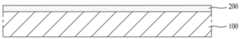
우선, 도 1a에서 알 수 있듯이, 기판(10) 상에 전면전극(20)을 형성한다.First, as shown in FIG. 1A, a
다음, 도 1b에서 알 수 있듯이, 상기 전면전극(20) 상에 반도체층(30)을 형성한다.Next, as shown in FIG. 1B, the
다음, 도 1c에서 알 수 있듯이, 상기 반도체층(30) 상에 투명도전층(40)을 형성한다.Next, as shown in FIG. 1C, a transparent
다음, 도 1d에서 알 수 있듯이, 상기 투명도전층(40) 상에 후면전극(60)을 형성한다.Next, as shown in FIG. 1D, a
여기서, 상기 후면전극(60)은 알루미늄(Al) 또는 은(Ag)과 같은 금속을 상기 투명도전층(40) 상에 인쇄한 후 소정의 온도로 소성하여 형성하게 되는데, 상기 소성 공정시 상기 후면전극(60)을 구성하는 Al 또는 Ag와 같은 금속이 산화되어 상기 후면전극(60)과 투명도전층(40) 사이에 후면전극 산화물(65)이 형성되게 된다.The
이와 같은 후면전극 산화물(65)은 알루미늄 산화물 또는 은 산화물로 이루어지는데, 이와 같은 산화물은 저항이 커서 후면전극(60)의 저항을 증가시켜 결국 태양전지의 효율을 저하시키는 단점이 있다.The
본 발명은 전술한 종래의 박막형 태양전지의 문제점을 해결하기 위해 고안된 것으로서, 본 발명은 후면전극과 투명도전층 사이에 버퍼층을 형성함으로써 후면전극과 투명도전층 사이에 저항이 큰 후면전극 산화물이 형성되지 않도록 하여 전지효율이 상승되는 박막형 태양전지 및 그 제조방법을 제공함을 목적으로 한다.The present invention has been devised to solve the problems of the conventional thin film solar cell described above, and it is an object of the present invention to provide a buffer layer between a back electrode and a transparent conductive layer so that a back electrode oxide having a high resistance is not formed between a back electrode and a transparent conductive layer Thereby improving the cell efficiency and a method of manufacturing the same.
본 발명은 상기 목적을 달성하기 위해서, 기판 상에 형성된 전면전극; 상기 전면전극 상에 형성된 반도체층; 상기 반도체층 상에 형성된 투명도전층; 상기 투명도전층 상에 형성된 후면전극; 및 상기 투명도전층과 후면전극 사이에 형성되어, 상기 후면전극의 전기적 저항을 감소시킴과 더불어 상기 투명도전층과 후면전극 사이의 접착력을 증진시키는 버퍼층을 포함하여 이루어진 박막형 태양전지를 제공한다.In order to achieve the above object, the present invention provides a plasma display panel comprising: a front electrode formed on a substrate; A semiconductor layer formed on the front electrode; A transparent conductive layer formed on the semiconductor layer; A rear electrode formed on the transparent conductive layer; And a buffer layer formed between the transparent conductive layer and the rear electrode to reduce an electrical resistance of the rear electrode and to enhance adhesion between the transparent conductive layer and the rear electrode.
상기 버퍼층은 상기 후면전극을 구성하는 물질보다 산화도가 큰 물질을 포함하여 이루어질 수 있다.The buffer layer may include a material having a higher degree of oxidation than the material of the rear electrode.
상기 버퍼층은 상기 후면전극을 구성하는 물질보다 산화도가 큰 금속물질 및 상기 금속물질의 산화물이 순서대로 적층되어 이루어질 수 있다.The buffer layer may be formed by sequentially laminating a metal material having a higher oxidation degree than the material of the rear electrode and an oxide of the metal material.
상기 버퍼층을 구성하는 금속물질의 산화물은 상기 후면전극의 산화물보다 전기적 저항이 작다.The oxide of the metal material constituting the buffer layer has a smaller electrical resistance than the oxide of the rear electrode.
상기 버퍼층을 구성하는 금속물질의 산화물은 상기 투명도전층과 동일한 물 질로 이루어질 수 있다.The oxide of the metal material constituting the buffer layer may be made of the same material as the transparent conductive layer.
상기 금속물질의 산화물 및 상기 투명도전층은 ZnO로 이루어질 수 있다.The oxide of the metal material and the transparent conductive layer may be made of ZnO.
본 발명은 또한, 기판 상에 전면전극을 형성하는 공정; 상기 전면전극 상에 반도체층을 형성하는 공정; 상기 반도체층 상에 투명도전층을 형성하는 공정; 상기 투명도전층 상에 버퍼층을 형성하는 공정; 및 상기 버퍼층 상에 후면전극을 형성하는 공정을 포함하여 이루어진 박막형 태양전지의 제조방법을 제공한다.The present invention also provides a method of manufacturing a semiconductor device, comprising: forming a front electrode on a substrate; Forming a semiconductor layer on the front electrode; Forming a transparent conductive layer on the semiconductor layer; Forming a buffer layer on the transparent conductive layer; And forming a rear electrode on the buffer layer. The present invention also provides a method of manufacturing a thin film solar cell.
상기 버퍼층을 형성하는 공정은 상기 투명도전층 상에 상기 후면전극을 구성하는 물질보다 산화도가 큰 금속물질 및 상기 금속물질의 산화물을 순서대로 형성하는 공정으로 이루어질 수 있다.The buffer layer may be formed by sequentially forming a metal material having a higher oxidation degree than the material of the rear electrode and an oxide of the metal material on the transparent conductive layer.
상기 후면전극을 형성하는 공정은 후면전극물질을 인쇄한 후 소성하는 공정으로 이루어지고, 상기 버퍼층을 구성하는 금속물질의 산화물은 상기 후면전극을 형성하기 위한 소성 공정시 상기 금속물질이 산화되어 형성될 수 있다.The step of forming the rear electrode comprises a step of printing and then firing the rear electrode material, and the oxide of the metal material constituting the buffer layer is formed by oxidizing the metal material during the firing process for forming the rear electrode .
상기 버퍼층을 구성하는 금속물질은 상기 투명도전층 상에 별도의 층을 적층하여 형성할 수 있다.The metal material constituting the buffer layer may be formed by laminating a separate layer on the transparent conductive layer.
상기 버퍼층을 구성하는 금속물질을 형성하는 공정은 불활성가스분위기에서 Zn을 표적으로 하여 스퍼터링법을 이용하여 Zn을 형성하는 공정으로 이루어질 수 있다.The step of forming the metal material constituting the buffer layer may include a step of forming Zn by sputtering with Zn as an target in an inert gas atmosphere.
상기 투명도전층을 형성하는 공정은 산소분위기에서 Zn을 표적으로 하여 스퍼터링법을 이용하여 ZnO를 형성하는 공정으로 이루어지고, 상기 투명도전층을 형성하는 공정 및 상기 버퍼층을 구성하는 금속물질을 형성하는 공정은 동일한 스퍼 터링 장비에서 연속공정으로 수행할 수 있다.Wherein the step of forming the transparent conductive layer comprises a step of forming ZnO by sputtering with Zn as the target in an oxygen atmosphere and the step of forming the transparent conductive layer and the step of forming the metal material constituting the buffer layer Can be performed in a continuous process in the same sputtering equipment.
상기 버퍼층을 구성하는 금속물질을 형성하는 공정은 수소분위기에서 Zn을 함유하는 가스를 원료로 하여 화학기상증착법 또는 원자층증착법을 이용하여 Zn을 형성하는 공정으로 이루어질 수 있다.The step of forming the metal material constituting the buffer layer may include a step of forming Zn by a chemical vapor deposition method or an atomic layer deposition method using a gas containing Zn as a raw material in a hydrogen atmosphere.
상기 버퍼층을 구성하는 금속물질은 상기 투명도전층의 상부를 환원시켜 형성할 수 있다.The metal material constituting the buffer layer may be formed by reducing an upper portion of the transparent conductive layer.
상기 투명도전층의 상부를 환원시키는 공정은 수소 플라즈마 처리를 수행하여 상기 투명도전층에 함유된 산소와 플라즈마 처리시 공급되는 수소를 반응시키는 공정으로 이루어질 수 있다.The step of reducing the upper part of the transparent conductive layer may include a step of performing a hydrogen plasma treatment to react oxygen contained in the transparent conductive layer with hydrogen supplied in the plasma treatment.
상기 버퍼층을 구성하는 금속물질의 산화물은 상기 후면전극의 산화물보다 전기적 저항이 작다.The oxide of the metal material constituting the buffer layer has a smaller electrical resistance than the oxide of the rear electrode.
상기와 같은 본 발명에 따르면 다음과 같은 효과가 있다.According to the present invention as described above, the following effects can be obtained.
첫째, 본 발명은 투명도전층과 후면전극 사이에 버퍼층을 형성함으로써, 후면전극의 전기적 저항을 감소시킴과 더불어 투명도전층과 후면전극 사이의 접착력이 증진되는 효과가 있다.First, by forming a buffer layer between the transparent conductive layer and the rear electrode, the present invention can reduce the electrical resistance of the rear electrode and improve the adhesion between the transparent conductive layer and the rear electrode.
구체적으로는, 후면전극을 구성하는 물질보다 산화도가 큰 금속물질을 포함하여 버퍼층을 구성함으로써 후면전극 형성을 위한 소성 공정시 종래와 같이 전기저항이 큰 후면전극 산화물이 형성되지 않고 전기저항이 매우 작은 금속물질의 산화물이 형성되도록 하여 후면전극의 전기적 저항을 감소시켜 태양전지의 효율이 증 진되게 되며, 또한, 버퍼층을 구성하는 금속물질의 산화물에 의해서 투명도전층과 후면전극 사이의 접착력이 증진되게 된다.Specifically, a buffer layer including a metal material having a higher degree of oxidation than a material forming the rear electrode is formed, so that a rear electrode oxide having a large electrical resistance is not formed in a sintering process for forming a rear electrode, The efficiency of the solar cell is improved by reducing the electrical resistance of the rear electrode. Further, since the oxide of the metal material constituting the buffer layer enhances the adhesion between the transparent conductive layer and the rear electrode do.
둘째, 본 발명은 버퍼층을 구성하는 금속물질의 산화물과 투명도전층을 동일한 물질로 형성함으로써, 동일한 장비에서 연속공정으로 수행할 수 있거나 또는 투명도전층을 이용하여 버퍼층을 구성하는 금속물질을 형성할 수 있어 제조공정을 보다 용이하게 조절할 수 있는 장점이 있다.Second, the present invention can be carried out in a continuous process in the same equipment by forming the oxide of the metal material and the transparent conductive layer of the same material constituting the buffer layer, or the metal material constituting the buffer layer can be formed using the transparent conductive layer The manufacturing process can be more easily controlled.
이하, 도면을 참조로 본 발명의 바람직한 실시예에 대해서 상세히 설명하기로 한다.Hereinafter, preferred embodiments of the present invention will be described in detail with reference to the drawings.
<박막형 태양전지><Thin-film solar cell>
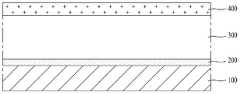
도 2는 본 발명의 일 실시예에 따른 박막형 태양전지의 개략적인 단면도이다.2 is a schematic cross-sectional view of a thin film solar cell according to an embodiment of the present invention.
도 2에서 알 수 있듯이, 본 발명의 일 실시예에 따른 박막형 태양전지는, 기판(100), 전면전극(200), 반도체층(300), 투명도전층(400), 버퍼층(500) 및 후면전극(600)을 포함하여 이루어진다.2, a thin film solar cell according to an exemplary embodiment of the present invention includes a
상기 기판(100)은 유리 또는 투명한 플라스틱으로 이루어진다.The
상기 전면전극(200)은 ZnO, ZnO:B, ZnO:Al, ZnO:H, SnO2, SnO2:F, 또는 ITO(Indium Tin Oxide) 등과 같은 투명한 도전물질을 이용하여 형성할 수 있다.The
상기 전면전극(200)은 텍스처(texturing) 가공공정 등을 통해 그 표면을 요철구조로 형성하는 것이 바람직하다. 상기 텍스처 가공공정이란 물질 표면을 울퉁불퉁한 요철구조로 형성하여 마치 직물의 표면과 같은 형상으로 가공하는 공정으로서, 포토리소그라피법(photolithography)을 이용한 식각공정, 화학용액을 이용한 이방성 식각공정(anisotropic etching), 또는 기계적 스크라이빙(mechanical scribing)을 이용한 홈 형성 공정 등을 통해 수행할 수 있다. 이와 같은 텍스처 가공공정을 상기 전면전극(200)에 수행할 경우 입사되는 태양광이 태양전지 외부로 반사되는 비율은 감소하게 되며, 그와 더불어 입사되는 태양광의 산란에 의해 태양전지 내부로 태양광이 흡수되는 비율은 증가하게 되어, 태양전지의 효율이 증진되는 효과가 있다.The
상기 반도체층(300)은 실리콘계 반도체물질을 이용하여 형성할 수 있다The
상기 반도체층(300)은 P형 반도체층, I형 반도체층 및 N형 반도체층이 순서대로 적층된 PIN구조로 형성하는데, 이와 같이 상기 반도체층(300)을 PIN구조로 형성하게 되면, I형 반도체층이 P형 반도체층과 N형 반도체층에 의해 공핍(depletion)이 되어 내부에 전기장이 발생하게 되고, 태양광에 의해 생성되는 정공 및 전자가 상기 전기장에 의해 드리프트(drift)되어 각각 P형 반도체층 및 N형 반도체층에서 수집되게 된다.The
상기 반도체층(300)을 PIN구조로 형성할 경우에는 상기 전면전극(200) 상부에 P형 반도체층을 형성하고 이어서 I형 반도체층 및 N형 반도체층을 형성하는 것이 바람직하다. 그 이유는 일반적으로 정공의 드리프트 이동도(drift mobility)가 전자의 드리프트 이동도에 의해 낮기 때문에 입사광에 의한 수집효율을 극대화하기 위해서 P형 반도체층을 수광면에 가깝게 형성하기 위함이다.When the
상기 투명도전층(400)은 ZnO와 같은 투명한 도전물질을 이용하여 형성한다.The transparent
상기 투명도전층(400)은 상기 반도체층(300)을 투과한 태양광을 다양한 각으로 산란시켜, 상기 후면전극(600)에서 반사되어 반도체층(300)으로 재입사되는 광의 비율을 증가시키게 된다.The transparent
상기 버퍼층(500)은 상기 투명도전층(400)과 후면전극(600) 사이에 형성되 어, 상기 후면전극(600)의 전기적 저항을 감소시킴과 더불어 상기 투명도전층(400)과 후면전극(600) 사이의 접착력을 증진시키는 역할을 한다.The
상기 버퍼층(500)은 상기 후면전극(600)을 구성하는 물질보다 산화도가 큰 물질, 바람직하게는 Zn과 같은 투명한 금속물질(510)을 포함하여 이루어진다. 따라서, 상기 후면전극(600) 형성을 위한 소성 공정시 종래와 같이 알루미늄 산화물 또는 은 산화물과 같은 전기저항이 큰 물질이 형성되지 않고 ZnO와 같은 전기저항이 매우 작은 금속물질(510)의 산화물(530)이 형성된다. 결국, Zn과 같은 금속물질(510) 및 ZnO와 같은 상기 금속물질(510)의 산화물(530)이 순서대로 적층되어 버퍼층(500)을 구성함으로써, 후면전극(600)의 전기적 저항이 감소되어 태양전지의 효율이 증진되게 된다. 또한, 상기 버퍼층을 구성하는 금속물질(510)의 산화물(530)은 상기 투명도전층(400)과 후면전극(600) 사이의 접착력을 증진시키는 역할을 수행하게 된다.The
상기 투명도전층(400)을 ZnO로 형성하고 상기 버퍼층(500)을 구성하는 금속물질(510) 및 금속물질(510)의 산화물(530)을 각각 Zn 및 ZnO로 형성함으로써, 상기 버퍼층(500)을 구성하는 금속물질(510)의 산화물(530)과 상기 투명도전층(400)을 동일한 물질로 형성할 경우 동일한 장비에서 연속공정으로 수행할 수 있거나(도 3a 내지 도 3f에 따른 제조방법 참조) 또는 투명도전층(400)을 이용하여 버퍼층(500)을 구성하는 금속물질(510)을 형성할 수 있는(도 4a 내지 도 4f에 따른 제조방법 참조) 등 제조공정을 보다 용이하게 조절할 수 있는 장점이 있으며, 이에 대해서는 후술하는 박막 태양전지의 제조방법을 참조하면 이해할 수 있을 것이다.The transparent
상기 후면전극(600)은 Ag, Al, Ag+Mo, Ag+Ni, Ag+Cu 등과 같은 금속을 이용하여 형성한다.The
<박막형 태양전지의 제조방법><Manufacturing Method of Thin Film Solar Cell>
도 3a 내지 도 3f는 본 발명의 일 실시예에 따른 박막형 태양 전지의 개략적 공정 단면도이다.3A to 3F are schematic sectional views of a thin film solar cell according to an embodiment of the present invention.
우선, 도 3a에서 알 수 있듯이, 기판(100) 상에 전면전극(200)을 형성한다.First, as shown in FIG. 3A, the
상기 전면전극(200)은 ZnO, ZnO:B, ZnO:Al, ZnO:H, SnO2, SnO2:F, 또는 ITO(Indium Tin Oxide) 등과 같은 투명한 도전물질을 스퍼터링(Sputtering)법 또는 MOCVD(Metal Organic Chemical Vapor Deposition)법 등을 이용하여 형성할 수 있다.The
상기 전면전극(200)은 태양광의 흡수율을 최대화하기 위해서 텍스처 가공공정 등을 통해 그 표면을 울퉁불퉁한 요철구조로 형성할 수 있다.In order to maximize the absorption rate of sunlight, the
다음, 도 3b에서 알 수 있듯이, 상기 전면전극(200) 상에 반도체층(300)을 형성한다.Next, as shown in FIG. 3B, the
상기 반도체층(300)은 실리콘계 반도체물질을 플라즈마 CVD법을 이용하여 P형 반도체층, I형 반도체층 및 N형 반도체층이 순서대로 적층된 PIN구조로 형성할 수 있다.The
다음, 도 3c에서 알 수 있듯이, 상기 반도체층(300) 상에 투명도전층(400)을 형성한다.Next, as shown in FIG. 3C, a transparent
상기 투명도전층(400)은 ZnO와 같은 투명한 도전물질을 스퍼터링(Sputtering)법 또는 MOCVD(Metal Organic Chemical Vapor Deposition)법 등을 이용하여 형성할 수 있다.The transparent
다음, 도 3d에서 알 수 있듯이, 상기 투명도전층(400) 상에 금속물질(510)을 형성한다.Next, as shown in FIG. 3D, a
상기 금속물질(510)은 후술하는 후면전극을 구성하는 물질보다 산화도가 큰 금속을 이용하여 형성하며, 그에 따라 후면전극 형성을 위한 소성공정시 후면전극의 산화물이 형성되는 대신에 상기 금속물질(510)의 산화물이 형성되게 된다.The
상기 금속물질(510)은 상기 투명도전층(400) 상에 별도의 층을 적층하여 형성하는데, 그 구체적인 형성방법으로는 스퍼터링법(Sputtering), 화학기상증착법(CVD) 또는 원자층증착법(ALD)을 들 수 있다.The
첫째, 상기 금속물질(510)은 상기 투명도전층(400) 상에 스퍼터링법(Sputtering)을 이용하여 형성할 수 있으며, 이 경우에는 전술한 도 3c 공정과 동일한 스퍼터링 장비에서 연속공정으로 수행할 수 있는 장점이 있다. 즉, 전술한 도 3c공정에서는 산소분위기에서 Zn을 표적(target)으로 하여 스퍼터링법을 이용하여 ZnO로 이루어진 투명도전층(400)을 형성하고, 도 3d공정에서는 아르곤과 같은 불활성가스분위기에서 Zn을 표적으로 하여 스퍼터링법을 이용하여 Zn으로 이루어진 금속물질(510)을 형성할 수 있기 때문에, 동일한 스퍼터링장비에서 공급하는 가스만을 변경함으로써, 도 3c 공정 및 도 3d 공정을 연속수행할 수 있게 된다.First, the
둘째, 상기 금속물질(510)은 상기 투명도전층(400) 상에 화학기상증착 법(CVD) 또는 원자층증착법(ALD)을 이용하여 형성할 수도 있다. 구체적으로는, 수소분위기에서 Zn(CH3)2 또는 Zn(C2H5)2을 원료로 하여 화학기상증착법 또는 원자층증착법을 이용하여 Zn으로 이루어진 금속물질(510)을 형성할 수 있으며, 이 경우에는 Zn(CH3)2 + H2 → Zn + 2(CH4) 또는 Zn(C2H5)2+ H2 → Zn + 2(C2H6)와 같은 반응을 통해 Zn으로 이루어진 금속물질(510)이 형성된다.Second, the
다음, 도 3e에서 알 수 있듯이, 상기 금속물질(510) 상에 후면전극물질(600a)을 형성한다.3E, a
상기 후면전극물질(600a)은 Ag, Al, Ag+Al, Ag+Mg, Ag+Mn, Ag+Sb, Ag+Zn, Ag+Mo, Ag+Ni, Ag+Cu, Ag+Al+Zn 등과 같은 금속을 스크린인쇄법(screen printing), 잉크젯인쇄법(inkjet printing), 그라비아인쇄법(gravure printing) 또는 미세접촉인쇄법(microcontact printing)을 이용하여 형성할 수 있다.The
상기 스크린 인쇄법은 스크린과 스퀴즈(squeeze)를 이용하여 대상물질을 작업물에 전이시켜 소정의 패턴을 형성하는 방법이고, 상기 잉크젯 인쇄법은 잉크젯을 이용하여 대상물질을 작업물에 분사하여 소정의 패턴을 형성하는 방법이고, 상기 그라비아 인쇄법은 오목판의 홈에 대상물질을 도포하고 그 대상물질을 다시 작업물에 전이시켜 소정의 패턴을 형성하는 방법이고, 상기 미세접촉 인쇄법은 소정의 금형을 이용하여 작업물에 대상물질 패턴을 형성하는 방법이다.The screen printing method is a method of forming a predetermined pattern by transferring a target material to a work using a screen and a squeeze. In the inkjet printing method, an object is sprayed onto a work using an inkjet, The gravure printing method is a method of applying a target material to a groove of a concave plate and transferring the target material to a workpiece again to form a predetermined pattern. The fine contact printing method is a method of forming a predetermined mold To form a target material pattern on a workpiece.
다음, 도 3f에서 알 수 있듯이, 상기 후면전극물질(600a)을 소성하여 후면전극(600)을 완성한다.Next, as shown in FIG. 3F, the
상기 후면전극물질(600a)의 소성 공정시 상기 금속물질(510)의 상부가 산화되어 상기 금속물질(510)의 산화물(530)이 형성되고, 그에 따라 금속물질(510) 및 금속물질(510)의 산화물(530)로 이루어진 버퍼층(500)이 형성된다.The upper portion of the
즉, 상기 금속물질(510)의 산화도가 상기 후면전극물질(600a)의 산화도보다 크기 때문에 상기 소성공정시 후면전극물질(600a)의 산화물이 형성되는 대신에 상기 금속물질(510)의 산화물이 형성되게 된다. 이때, 상기 금속물질(510)이 Zn으로 이루어진 경우 상기 금속물질(510)의 산화물은 ZnO로 이루어져, 종래의 후면전극 산화물과 비교할 때 전기적 저항이 매우 작기 때문에 후면전극(600)의 저항이 증가되는 것이 방지된다. 또한, 소성공정시 생성되는 금속물질(510)의 산화물(530)에 의해서 후면전극(600)과 투명도전층(400) 사이의 접착력도 크게 증가되게 된다.That is, since the degree of oxidation of the
도 4a 내지 도 4f는 본 발명의 다른 실시예에 따른 박막형 태양 전지의 개략적 공정 단면도로서, 금속물질(510)을 투명도전층(400) 상에 별도의 층으로 적층하는 대신에 투명도전층(400)의 상부를 환원시켜 금속물질(510)을 형성하는 것을 제외하고 전술한 도 3a 내지 도 3f에 따른 공정과 동일하다. 따라서, 동일한 부분에 대한 구체적인 설명은 생략한다.4A to 4F are schematic cross-sectional views of a thin film solar cell according to another embodiment of the present invention, in which a
우선, 도 4a에서 알 수 있듯이, 기판(100) 상에 전면전극(200)을 형성한다.As shown in FIG. 4A, the
다음, 도 4b에서 알 수 있듯이, 상기 전면전극(200) 상에 반도체층(300)을 형성한다.Next, as shown in FIG. 4B, the
다음, 도 4c에서 알 수 있듯이, 상기 반도체층(300) 상에 투명도전층(400)을 형성한다.Next, as shown in FIG. 4C, a transparent
상기 투명도전층(400)은 ZnO와 같은 투명한 도전물질을 스퍼터링(Sputtering)법 또는 MOCVD(Metal Organic Chemical Vapor Deposition)법 등을 이용하여 형성할 수 있다.The transparent
다음, 도 4d에서 알 수 있듯이, 상기 투명도전층(400)의 상부를 환원시켜 금속물질(510)을 형성한다.4D, an upper portion of the transparent
즉, 상기 투명도전층(400)에 수소 플라즈마 처리를 수행할 경우 상기 투명도전층(400)의 상부에서 상기 투명도전층(400)에 함유된 산소(O2)가 플라즈마 처리시 공급되는 수소(H2)가 반응하게 되며, 이에 따라 투명도전층(400)에서 산소가 빠져나가면서 투명도전층(400)의 상부가 금속물질(510)로 환원되게 된다. 예를 들면, 투명도전층(400)을 구성하는 ZnO에 수소 플라즈마 처리를 수행할 경우 ZnO + H2 → Zn + H2O와 같은 반응을 일으켜 상기 투명도전층(400)의 상부에 Zn으로 이루어진 금속물질(510)이 형성되게 된다.That is, when the hydrogen plasma treatment is performed on the transparent
다음, 도 4e에서 알 수 있듯이, 상기 금속물질(510) 상에 후면전극물질(600a)을 형성한다.4E, a
다음, 도 4f에서 알 수 있듯이, 상기 후면전극물질(600a)을 소성하여 후면전극(600)을 완성함과 동시에, 상기 후면전극물질(600a)의 소성 공정시 상기 금속물질(510)의 상부가 산화되어 금속물질(510) 및 금속물질(510)의 산화물(530)로 이루어진 버퍼층(500)이 형성된다.4F, the
도 1a 내지 도 1d는 종래의 박막형 태양전지의 개략적인 공정 단면도이다.1A to 1D are schematic sectional views of a conventional thin-film solar cell.
도 2는 본 발명의 일 실시예에 따른 박막형 태양전지의 개략적인 단면도이다.2 is a schematic cross-sectional view of a thin film solar cell according to an embodiment of the present invention.
도 3a 내지 도 3f는 본 발명의 일 실시예에 따른 박막형 태양 전지의 개략적 공정 단면도이다.3A to 3F are schematic sectional views of a thin film solar cell according to an embodiment of the present invention.
도 4a 내지 도 4f는 본 발명의 다른 실시예에 따른 박막형 태양 전지의 개략적 공정 단면도이다.4A to 4F are schematic sectional views of a thin film solar cell according to another embodiment of the present invention.
<도면의 주요부의 부호에 대한 설명>DESCRIPTION OF THE REFERENCE NUMERALS OF THE DRAWINGS FIG.
100: 기판 200: 전면전극100: substrate 200: front electrode
300: 반도체층 400: 투명도전층300: semiconductor layer 400: transparency layer
500: 버퍼층 510: 금속물질500: buffer layer 510: metal material
530: 금속물질의 산화물 600: 후면전극530: oxide of a metal material 600: rear electrode
Claims (18)
Translated fromKoreanPriority Applications (5)
| Application Number | Priority Date | Filing Date | Title |
|---|---|---|---|
| KR1020080015124AKR101448448B1 (en) | 2008-02-20 | 2008-02-20 | Thin film type Solar Cell and Method for manufacturing the same |
| CN2009100091387ACN101515606B (en) | 2008-02-20 | 2009-02-20 | Thin-film solar cell and manufacturing method thereof |
| TW098105555ATWI404217B (en) | 2008-02-20 | 2009-02-20 | Thin film type solar cell and manufacturing method thereof |
| US12/378,890US20090205709A1 (en) | 2008-02-20 | 2009-02-20 | Thin film type solar cell and method for manufacturing the same |
| US14/454,636US20140349442A1 (en) | 2008-02-20 | 2014-08-07 | Thin film type solar cell and method for manufacturing the same |
Applications Claiming Priority (1)
| Application Number | Priority Date | Filing Date | Title |
|---|---|---|---|
| KR1020080015124AKR101448448B1 (en) | 2008-02-20 | 2008-02-20 | Thin film type Solar Cell and Method for manufacturing the same |
Publications (2)
| Publication Number | Publication Date |
|---|---|
| KR20090089944A KR20090089944A (en) | 2009-08-25 |
| KR101448448B1true KR101448448B1 (en) | 2014-10-14 |
Family
ID=40953993
Family Applications (1)
| Application Number | Title | Priority Date | Filing Date |
|---|---|---|---|
| KR1020080015124AActiveKR101448448B1 (en) | 2008-02-20 | 2008-02-20 | Thin film type Solar Cell and Method for manufacturing the same |
Country Status (4)
| Country | Link |
|---|---|
| US (2) | US20090205709A1 (en) |
| KR (1) | KR101448448B1 (en) |
| CN (1) | CN101515606B (en) |
| TW (1) | TWI404217B (en) |
Families Citing this family (12)
| Publication number | Priority date | Publication date | Assignee | Title |
|---|---|---|---|---|
| US8160007B2 (en)* | 2007-11-20 | 2012-04-17 | Qualcomm Incorporated | Opportunistic uplink scheduling |
| US8547857B2 (en)* | 2007-11-20 | 2013-10-01 | Qualcomm Incorporated | Opportunistic uplink scheduling |
| KR101103914B1 (en)* | 2009-11-06 | 2012-01-12 | 엘지이노텍 주식회사 | Solar cell and manufacturing method thereof |
| EP2325848B1 (en) | 2009-11-11 | 2017-07-19 | Samsung Electronics Co., Ltd. | Conductive paste and solar cell |
| KR102071006B1 (en)* | 2009-11-11 | 2020-01-30 | 삼성전자주식회사 | Conductive paste and solar cell |
| KR101132032B1 (en)* | 2010-08-11 | 2012-04-02 | 삼성에스디아이 주식회사 | Electrode for photoelectric conversion device, method of preparing the same and photoelectric conversion device comprising the same |
| US9876129B2 (en)* | 2012-05-10 | 2018-01-23 | International Business Machines Corporation | Cone-shaped holes for high efficiency thin film solar cells |
| US9153729B2 (en) | 2012-11-26 | 2015-10-06 | International Business Machines Corporation | Atomic layer deposition for photovoltaic devices |
| US8889466B2 (en) | 2013-04-12 | 2014-11-18 | International Business Machines Corporation | Protective insulating layer and chemical mechanical polishing for polycrystalline thin film solar cells |
| CN103606576B (en)* | 2013-10-21 | 2016-06-08 | 溧阳市东大技术转移中心有限公司 | A kind of solar cell |
| US10062636B2 (en)* | 2016-06-27 | 2018-08-28 | Newport Fab, Llc | Integration of thermally conductive but electrically isolating layers with semiconductor devices |
| US10490649B2 (en)* | 2017-05-30 | 2019-11-26 | Taiwan Semiconductor Manufacturing Company, Ltd. | Method of fabricating semiconductor device with adhesion layer |
Citations (3)
| Publication number | Priority date | Publication date | Assignee | Title |
|---|---|---|---|---|
| KR100237661B1 (en)* | 1994-08-24 | 2000-01-15 | 미다라이 후지오 | Back reflective layer, method of forming the same, and photovoltaic device using the back reflective layer and manufacturing method thereof |
| KR100251071B1 (en) | 1995-09-26 | 2000-04-15 | 미다라이 후지오 | Method of producing a photovoltaic device |
| KR20080003625A (en)* | 2006-07-03 | 2008-01-08 | 엘지전자 주식회사 | Thin film type solar cell and manufacturing method thereof |
Family Cites Families (9)
| Publication number | Priority date | Publication date | Assignee | Title |
|---|---|---|---|---|
| US4104084A (en)* | 1977-06-06 | 1978-08-01 | The United States Of America As Represented By The Administrator Of The National Aeronautics And Space Administration | Solar cells having integral collector grids |
| US4602120A (en)* | 1983-11-25 | 1986-07-22 | Atlantic Richfield Company | Solar cell manufacture |
| US5069968A (en)* | 1990-12-20 | 1991-12-03 | Ford Motor Company | Laminated glazing unit having improved interfacial adhesion |
| JP2771414B2 (en)* | 1992-12-28 | 1998-07-02 | キヤノン株式会社 | Solar cell manufacturing method |
| US5569332A (en)* | 1995-08-07 | 1996-10-29 | United Solar Systems Corporation | Optically enhanced photovoltaic back reflector |
| US6132589A (en)* | 1998-09-10 | 2000-10-17 | Ga-Tek Inc. | Treated copper foil and process for making treated copper foil |
| US6632993B2 (en)* | 2000-10-05 | 2003-10-14 | Kaneka Corporation | Photovoltaic module |
| US7763794B2 (en)* | 2004-12-01 | 2010-07-27 | Palo Alto Research Center Incorporated | Heterojunction photovoltaic cell |
| WO2006098185A1 (en)* | 2005-03-15 | 2006-09-21 | Kaneka Corporation | Process for producing substrate for thin-film photoelectric transducer, and thin-film photoelectric transducer |
- 2008
- 2008-02-20KRKR1020080015124Apatent/KR101448448B1/enactiveActive
- 2009
- 2009-02-20USUS12/378,890patent/US20090205709A1/ennot_activeAbandoned
- 2009-02-20CNCN2009100091387Apatent/CN101515606B/enactiveActive
- 2009-02-20TWTW098105555Apatent/TWI404217B/enactive
- 2014
- 2014-08-07USUS14/454,636patent/US20140349442A1/ennot_activeAbandoned
Patent Citations (3)
| Publication number | Priority date | Publication date | Assignee | Title |
|---|---|---|---|---|
| KR100237661B1 (en)* | 1994-08-24 | 2000-01-15 | 미다라이 후지오 | Back reflective layer, method of forming the same, and photovoltaic device using the back reflective layer and manufacturing method thereof |
| KR100251071B1 (en) | 1995-09-26 | 2000-04-15 | 미다라이 후지오 | Method of producing a photovoltaic device |
| KR20080003625A (en)* | 2006-07-03 | 2008-01-08 | 엘지전자 주식회사 | Thin film type solar cell and manufacturing method thereof |
Also Published As
| Publication number | Publication date |
|---|---|
| US20090205709A1 (en) | 2009-08-20 |
| TWI404217B (en) | 2013-08-01 |
| CN101515606B (en) | 2011-06-01 |
| KR20090089944A (en) | 2009-08-25 |
| US20140349442A1 (en) | 2014-11-27 |
| TW200937653A (en) | 2009-09-01 |
| CN101515606A (en) | 2009-08-26 |
Similar Documents
| Publication | Publication Date | Title |
|---|---|---|
| KR101448448B1 (en) | Thin film type Solar Cell and Method for manufacturing the same | |
| RU2435251C2 (en) | Front electrode with layer of thin metal film and high-work function buffer layer for use in photovoltaic device and production method thereof | |
| JP2017143279A (en) | Photoelectric conversion device | |
| KR20120052310A (en) | Solar cell front contact doping | |
| KR20100021045A (en) | Thin film type solar cell and method for manufacturing the same | |
| CN105580142A (en) | Solar battery | |
| CN103081123A (en) | Device for generating solar power and method for manufacturing same | |
| WO2011042328A1 (en) | Method of coating a substrate | |
| KR101368902B1 (en) | Thin film type Solar Cell and Method for manufacturing the same | |
| KR101476120B1 (en) | Thin film solar cell and its manufacturing method | |
| KR20090067350A (en) | Thin film type solar cell and manufacturing method thereof | |
| CN101779292A (en) | Thin film type solar cell and method for manufacturing the same | |
| JP2012530377A (en) | Solar cell and manufacturing method thereof | |
| KR101000051B1 (en) | Thin film type solar cell and manufacturing method thereof | |
| KR101415322B1 (en) | Thin film solar cell and its manufacturing method | |
| KR102049604B1 (en) | Solar cell and Method of manufacturing the same | |
| US20110155229A1 (en) | Solar cell and method for manufacturing the same | |
| CN104350612A (en) | Solar cell and method for manufacturing same | |
| KR20130061346A (en) | Solar cell and method of manufacturing the same | |
| KR101033286B1 (en) | Thin film type solar cell and manufacturing method thereof | |
| KR101547342B1 (en) | Method for manufacturing of thin film type solar cell | |
| KR20170097440A (en) | Solar cells and manufacturing method for the same | |
| KR101643231B1 (en) | Solar Cell and method of manufacturing the same | |
| KR101854236B1 (en) | Solar Cell and method of manufacturing the same | |
| KR101073832B1 (en) | Method for manufacturing thin film type Solar Cell |
Legal Events
| Date | Code | Title | Description |
|---|---|---|---|
| PA0109 | Patent application | Patent event code:PA01091R01D Comment text:Patent Application Patent event date:20080220 | |
| PG1501 | Laying open of application | ||
| A201 | Request for examination | ||
| PA0201 | Request for examination | Patent event code:PA02012R01D Patent event date:20130213 Comment text:Request for Examination of Application Patent event code:PA02011R01I Patent event date:20080220 Comment text:Patent Application | |
| E902 | Notification of reason for refusal | ||
| PE0902 | Notice of grounds for rejection | Comment text:Notification of reason for refusal Patent event date:20140220 Patent event code:PE09021S01D | |
| E701 | Decision to grant or registration of patent right | ||
| PE0701 | Decision of registration | Patent event code:PE07011S01D Comment text:Decision to Grant Registration Patent event date:20140825 | |
| GRNT | Written decision to grant | ||
| PR0701 | Registration of establishment | Comment text:Registration of Establishment Patent event date:20141001 Patent event code:PR07011E01D | |
| PR1002 | Payment of registration fee | Payment date:20141001 End annual number:3 Start annual number:1 | |
| PG1601 | Publication of registration | ||
| FPAY | Annual fee payment | Payment date:20180817 Year of fee payment:5 | |
| PR1001 | Payment of annual fee | Payment date:20180817 Start annual number:5 End annual number:5 | |
| PR1001 | Payment of annual fee | Payment date:20201005 Start annual number:7 End annual number:7 | |
| PR1001 | Payment of annual fee | Payment date:20210823 Start annual number:8 End annual number:8 | |
| PR1001 | Payment of annual fee | Payment date:20220822 Start annual number:9 End annual number:9 | |
| PR1001 | Payment of annual fee | Payment date:20230821 Start annual number:10 End annual number:10 | |
| PR1001 | Payment of annual fee | Payment date:20240826 Start annual number:11 End annual number:11 |