KR101447342B1 - Array substrate and manufacturing method thereof, liquid crystal panel, and display - Google Patents
Array substrate and manufacturing method thereof, liquid crystal panel, and displayDownload PDFInfo
- Publication number
- KR101447342B1 KR101447342B1KR1020127028554AKR20127028554AKR101447342B1KR 101447342 B1KR101447342 B1KR 101447342B1KR 1020127028554 AKR1020127028554 AKR 1020127028554AKR 20127028554 AKR20127028554 AKR 20127028554AKR 101447342 B1KR101447342 B1KR 101447342B1
- Authority
- KR
- South Korea
- Prior art keywords
- layer
- metal layer
- isolation buffer
- source
- buffer layer
- Prior art date
- Legal status (The legal status is an assumption and is not a legal conclusion. Google has not performed a legal analysis and makes no representation as to the accuracy of the status listed.)
- Active
Links
Images


Classifications
- H—ELECTRICITY
- H10—SEMICONDUCTOR DEVICES; ELECTRIC SOLID-STATE DEVICES NOT OTHERWISE PROVIDED FOR
- H10D—INORGANIC ELECTRIC SEMICONDUCTOR DEVICES
- H10D30/00—Field-effect transistors [FET]
- H10D30/60—Insulated-gate field-effect transistors [IGFET]
- H10D30/67—Thin-film transistors [TFT]
- H10D30/6729—Thin-film transistors [TFT] characterised by the electrodes
- H10D30/6737—Thin-film transistors [TFT] characterised by the electrodes characterised by the electrode materials
- G—PHYSICS
- G02—OPTICS
- G02F—OPTICAL DEVICES OR ARRANGEMENTS FOR THE CONTROL OF LIGHT BY MODIFICATION OF THE OPTICAL PROPERTIES OF THE MEDIA OF THE ELEMENTS INVOLVED THEREIN; NON-LINEAR OPTICS; FREQUENCY-CHANGING OF LIGHT; OPTICAL LOGIC ELEMENTS; OPTICAL ANALOGUE/DIGITAL CONVERTERS
- G02F1/00—Devices or arrangements for the control of the intensity, colour, phase, polarisation or direction of light arriving from an independent light source, e.g. switching, gating or modulating; Non-linear optics
- G02F1/01—Devices or arrangements for the control of the intensity, colour, phase, polarisation or direction of light arriving from an independent light source, e.g. switching, gating or modulating; Non-linear optics for the control of the intensity, phase, polarisation or colour
- G02F1/13—Devices or arrangements for the control of the intensity, colour, phase, polarisation or direction of light arriving from an independent light source, e.g. switching, gating or modulating; Non-linear optics for the control of the intensity, phase, polarisation or colour based on liquid crystals, e.g. single liquid crystal display cells
- G02F1/133—Constructional arrangements; Operation of liquid crystal cells; Circuit arrangements
- G02F1/136—Liquid crystal cells structurally associated with a semi-conducting layer or substrate, e.g. cells forming part of an integrated circuit
- G02F1/1362—Active matrix addressed cells
- G02F1/136286—Wiring, e.g. gate line, drain line
- G—PHYSICS
- G02—OPTICS
- G02F—OPTICAL DEVICES OR ARRANGEMENTS FOR THE CONTROL OF LIGHT BY MODIFICATION OF THE OPTICAL PROPERTIES OF THE MEDIA OF THE ELEMENTS INVOLVED THEREIN; NON-LINEAR OPTICS; FREQUENCY-CHANGING OF LIGHT; OPTICAL LOGIC ELEMENTS; OPTICAL ANALOGUE/DIGITAL CONVERTERS
- G02F1/00—Devices or arrangements for the control of the intensity, colour, phase, polarisation or direction of light arriving from an independent light source, e.g. switching, gating or modulating; Non-linear optics
- G02F1/01—Devices or arrangements for the control of the intensity, colour, phase, polarisation or direction of light arriving from an independent light source, e.g. switching, gating or modulating; Non-linear optics for the control of the intensity, phase, polarisation or colour
- G02F1/13—Devices or arrangements for the control of the intensity, colour, phase, polarisation or direction of light arriving from an independent light source, e.g. switching, gating or modulating; Non-linear optics for the control of the intensity, phase, polarisation or colour based on liquid crystals, e.g. single liquid crystal display cells
- G02F1/133—Constructional arrangements; Operation of liquid crystal cells; Circuit arrangements
- G02F1/136—Liquid crystal cells structurally associated with a semi-conducting layer or substrate, e.g. cells forming part of an integrated circuit
- G02F1/1362—Active matrix addressed cells
- G02F1/1368—Active matrix addressed cells in which the switching element is a three-electrode device
- H—ELECTRICITY
- H01—ELECTRIC ELEMENTS
- H01L—SEMICONDUCTOR DEVICES NOT COVERED BY CLASS H10
- H01L21/00—Processes or apparatus adapted for the manufacture or treatment of semiconductor or solid state devices or of parts thereof
- H01L21/02—Manufacture or treatment of semiconductor devices or of parts thereof
- H01L21/04—Manufacture or treatment of semiconductor devices or of parts thereof the devices having potential barriers, e.g. a PN junction, depletion layer or carrier concentration layer
- H01L21/18—Manufacture or treatment of semiconductor devices or of parts thereof the devices having potential barriers, e.g. a PN junction, depletion layer or carrier concentration layer the devices having semiconductor bodies comprising elements of Group IV of the Periodic Table or AIIIBV compounds with or without impurities, e.g. doping materials
- H01L21/28—Manufacture of electrodes on semiconductor bodies using processes or apparatus not provided for in groups H01L21/20 - H01L21/268
- H01L21/283—Deposition of conductive or insulating materials for electrodes conducting electric current
- H01L21/285—Deposition of conductive or insulating materials for electrodes conducting electric current from a gas or vapour, e.g. condensation
- H01L21/28506—Deposition of conductive or insulating materials for electrodes conducting electric current from a gas or vapour, e.g. condensation of conductive layers
- H01L21/28512—Deposition of conductive or insulating materials for electrodes conducting electric current from a gas or vapour, e.g. condensation of conductive layers on semiconductor bodies comprising elements of Group IV of the Periodic Table
- H01L21/2855—Deposition of conductive or insulating materials for electrodes conducting electric current from a gas or vapour, e.g. condensation of conductive layers on semiconductor bodies comprising elements of Group IV of the Periodic Table by physical means, e.g. sputtering, evaporation
- H—ELECTRICITY
- H10—SEMICONDUCTOR DEVICES; ELECTRIC SOLID-STATE DEVICES NOT OTHERWISE PROVIDED FOR
- H10D—INORGANIC ELECTRIC SEMICONDUCTOR DEVICES
- H10D30/00—Field-effect transistors [FET]
- H10D30/60—Insulated-gate field-effect transistors [IGFET]
- H10D30/67—Thin-film transistors [TFT]
- H10D30/6729—Thin-film transistors [TFT] characterised by the electrodes
- H10D30/6737—Thin-film transistors [TFT] characterised by the electrodes characterised by the electrode materials
- H10D30/6739—Conductor-insulator-semiconductor electrodes
- H—ELECTRICITY
- H10—SEMICONDUCTOR DEVICES; ELECTRIC SOLID-STATE DEVICES NOT OTHERWISE PROVIDED FOR
- H10D—INORGANIC ELECTRIC SEMICONDUCTOR DEVICES
- H10D30/00—Field-effect transistors [FET]
- H10D30/60—Insulated-gate field-effect transistors [IGFET]
- H10D30/67—Thin-film transistors [TFT]
- H10D30/674—Thin-film transistors [TFT] characterised by the active materials
- H10D30/6741—Group IV materials, e.g. germanium or silicon carbide
- H10D30/6743—Silicon
- H—ELECTRICITY
- H10—SEMICONDUCTOR DEVICES; ELECTRIC SOLID-STATE DEVICES NOT OTHERWISE PROVIDED FOR
- H10D—INORGANIC ELECTRIC SEMICONDUCTOR DEVICES
- H10D86/00—Integrated devices formed in or on insulating or conducting substrates, e.g. formed in silicon-on-insulator [SOI] substrates or on stainless steel or glass substrates
- H10D86/40—Integrated devices formed in or on insulating or conducting substrates, e.g. formed in silicon-on-insulator [SOI] substrates or on stainless steel or glass substrates characterised by multiple TFTs
- H10D86/441—Interconnections, e.g. scanning lines
- H—ELECTRICITY
- H10—SEMICONDUCTOR DEVICES; ELECTRIC SOLID-STATE DEVICES NOT OTHERWISE PROVIDED FOR
- H10D—INORGANIC ELECTRIC SEMICONDUCTOR DEVICES
- H10D86/00—Integrated devices formed in or on insulating or conducting substrates, e.g. formed in silicon-on-insulator [SOI] substrates or on stainless steel or glass substrates
- H10D86/40—Integrated devices formed in or on insulating or conducting substrates, e.g. formed in silicon-on-insulator [SOI] substrates or on stainless steel or glass substrates characterised by multiple TFTs
- H10D86/60—Integrated devices formed in or on insulating or conducting substrates, e.g. formed in silicon-on-insulator [SOI] substrates or on stainless steel or glass substrates characterised by multiple TFTs wherein the TFTs are in active matrices
- H—ELECTRICITY
- H10—SEMICONDUCTOR DEVICES; ELECTRIC SOLID-STATE DEVICES NOT OTHERWISE PROVIDED FOR
- H10H—INORGANIC LIGHT-EMITTING SEMICONDUCTOR DEVICES HAVING POTENTIAL BARRIERS
- H10H20/00—Individual inorganic light-emitting semiconductor devices having potential barriers, e.g. light-emitting diodes [LED]
- H10H20/062—Light-emitting semiconductor devices having field effect type light-emitting regions, e.g. light-emitting High-Electron Mobility Transistors
- H—ELECTRICITY
- H10—SEMICONDUCTOR DEVICES; ELECTRIC SOLID-STATE DEVICES NOT OTHERWISE PROVIDED FOR
- H10H—INORGANIC LIGHT-EMITTING SEMICONDUCTOR DEVICES HAVING POTENTIAL BARRIERS
- H10H29/00—Integrated devices, or assemblies of multiple devices, comprising at least one light-emitting semiconductor element covered by group H10H20/00
- H10H29/10—Integrated devices comprising at least one light-emitting semiconductor component covered by group H10H20/00
Landscapes
- Physics & Mathematics (AREA)
- Nonlinear Science (AREA)
- Engineering & Computer Science (AREA)
- Microelectronics & Electronic Packaging (AREA)
- General Physics & Mathematics (AREA)
- Optics & Photonics (AREA)
- Mathematical Physics (AREA)
- Chemical & Material Sciences (AREA)
- Crystallography & Structural Chemistry (AREA)
- Computer Hardware Design (AREA)
- Power Engineering (AREA)
- Manufacturing & Machinery (AREA)
- Condensed Matter Physics & Semiconductors (AREA)
- Thin Film Transistor (AREA)
- Devices For Indicating Variable Information By Combining Individual Elements (AREA)
- Liquid Crystal (AREA)
- Electrodes Of Semiconductors (AREA)
Abstract
Translated fromKoreanDescription
Translated fromKorean본 발명은 어레이 기판 및 그 제조 방법, 액정 패널, 디스플레이에 관한 것이다.The present invention relates to an array substrate, a manufacturing method thereof, a liquid crystal panel, and a display.
종래, 통상적으로 알려져 있는 디스플레이로는, 액정 디스플레이, 전자 페이퍼, OLED(Organic Light-Emitting Diode, 유기 발광 다이오드) 디스플레이 등이 있다.Conventionally known displays include a liquid crystal display, an electronic paper, an OLED (Organic Light-Emitting Diode) display, and the like.
액정 디스플레이를 예로 하는 경우, 액정 디스플레이에서, 화소 스위칭 소자로서의 TFT(Thin Film Transistor, 박막 트랜지스터) 구조에서의 게이트 전극과 소스·드레인 전극은, 어레이 기판 상의 금속 전극으로서, 낮은 저항, 기판 및 다른 층(예를 들어, a-Si(아몰퍼스 실리콘), 도프 아몰퍼스 실리콘층)과의 좋은 점착성, a-Si층에서 이온 확산이 발생하지 않고, 화소 전극과의 접촉 저항이 낮으며, 에칭하기 쉽고, CVD(Chemical Vapor Deposition, 화학 기상 증착법)에 의해 막을 형성하는 과정에서 힐록(hillock)이 발생하지 않으며, 산화되기 어려운 등의 양호한 특성이 요구된다.In the case of a liquid crystal display as an example, in a liquid crystal display, a gate electrode and a source / drain electrode in a TFT (Thin Film Transistor) structure as a pixel switching element are a metal electrode on an array substrate, (For example, a-Si (amorphous silicon), a doped amorphous silicon layer), ion diffusion in the a-Si layer does not occur, contact resistance with the pixel electrode is low, (Hillock) is not generated in the process of forming a film by chemical vapor deposition (CVD), and good characteristics such as difficulty in oxidation are required.
TFT- LCD(액정 디스플레이)의 산업화의 초기에서, 금속 전극 배선에 사용되는 주된 재료로서, 예를 들어, 크롬(Cr), 몰리브덴(Mo), 탄탈(Ta) 등의 융점이 높은 금속이 있다.In the early stage of the industrialization of TFT-LCD (liquid crystal display), metals having high melting points such as chromium (Cr), molybdenum (Mo), tantalum (Ta)
액정 패널의 크기의 증가에 따라서, 금속 전극의 저항을 저감시키는 것이 요구되고 있다. 이 때문에, 금속 알루미늄(Al)이 널리 사용되고 있지만, 제조 공정 중에서 힐록 현상이 발생하기 쉬운 동시에, Al 이온이 a-Si층으로 확산되기 쉬우므로, 순수 알루미늄 대신에, 예를 들어 Al-Nd(알루미늄 네오디뮴 합금), Al-Ce(알루미늄 세륨 합금), Al-Nd-Mo(알루미늄 네오디뮴 몰리브덴 합금) 등의 알루미늄 합금을 사용하고 있다.As the size of the liquid crystal panel increases, it is required to reduce the resistance of the metal electrode. For this reason, although metal aluminum (Al) is widely used, a hillock phenomenon easily occurs in the manufacturing process and Al ions are apt to diffuse into the a-Si layer. Therefore, Aluminum alloy such as Al-Nd-Mo (neodymium alloy), Al-Ce (aluminum cerium alloy) and Al-Nd-Mo (aluminum neodymium molybdenum alloy).
액정 패널의 크기가 더 커지는 것과, 고속의 구동과 높은 해상도(4K*2K)가 요구되는 것에 수반하여, 저항률이 더 낮은 금속 구리 Cu가, TFT 구조에서의 금속 전극으로서 사용되기 시작하였다.With the increase in the size of the liquid crystal panel and the demand for high-speed driving and high resolution (4K * 2K), metal copper Cu having a lower resistivity has started to be used as a metal electrode in a TFT structure.
이상과 같은 액정 디스플레이의 TFT 구조를 실현하는 과정에서, 발명자는 종래의 기술에 적어도 이하와 같은 문제가 존재하는 것을 발견하였다. 우선, Cu와 기판 사이의 점착성이 낮으므로, 박리되기 쉽다. 그리고, Cu가 a-Si, 혹은 N+a-Si 박막층에 접할 때에, Cu 이온은 실리콘(Si)계의 박막으로 확산되기 쉬우므로, TFT 구조의 이온 성능에 영향을 미친다.In the process of realizing the TFT structure of the liquid crystal display as described above, the inventor found that at least the following problems exist in the conventional technology. First, since the adhesion between Cu and the substrate is low, it is likely to peel off. When Cu is in contact with the a-Si or N + a-Si thin film layer, Cu ions are easily diffused into a thin film of silicon (Si) system, which affects the ionic performance of the TFT structure.
본 발명은 TFT 구조에서의 금속 전극층의 금속 이온이, 활성층에 사용되는, 예를 들어 실리콘계 박막층으로 확산되는 것을 유효하게 방지하여, 금속 전극층과 기판 사이의 점착성을 높일 수 있는 어레이 기판 및 그 제조 방법, 액정 패널, 디스플레이를 제공한다.The present invention relates to an array substrate capable of effectively preventing metal ions of a metal electrode layer in a TFT structure from diffusing into, for example, a silicon-based thin film layer used in an active layer and thereby increasing adhesion between the metal electrode layer and a substrate, , A liquid crystal panel, and a display.
본 발명의 일 형태는, 기판과, 상기 기판에 형성되어 있는 게이트 금속층과, 활성층과, 소스·드레인 금속층을 구비하는 어레이 기판으로서, 상기 게이트 금속층의 두께 방향에서의 적어도 일측에 격리 버퍼층이 형성되고, 및/또는, 상기 소스·드레인 금속층의 두께 방향에서의 적어도 일측에 격리 버퍼층이 형성되고, 상기 격리 버퍼층은 산화몰리브덴에 의해 형성되는 어레이 기판을 제공한다.One aspect of the present invention is an array substrate comprising a substrate, a gate metal layer formed on the substrate, an active layer, and a source / drain metal layer, wherein an isolation buffer layer is formed on at least one side in the thickness direction of the gate metal layer And / or an isolation buffer layer is formed on at least one side in the thickness direction of the source / drain metal layer, and the isolation buffer layer is formed by molybdenum oxide.
본 발명의 다른 형태는, 베이스 기판 상에서의 게이트 금속층과, 활성층과, 소스·드레인 금속층을 구비하는 상기 어레이 기판을 제조하는 방법으로서,Another aspect of the present invention is a method of manufacturing the array substrate including a gate metal layer, an active layer, and a source / drain metal layer on a base substrate,
게이트 금속층에서의 적어도 일측에, 해당 게이트 금속층과 마찬가지인 패턴을 갖는 격리 버퍼층을 형성하고, 및/또는,An isolation buffer layer having a pattern similar to that of the gate metal layer is formed on at least one side of the gate metal layer and /
소스·드레인 금속층에서의 적어도 일측에, 상기 소스·드레인 금속층과 마찬가지인 패턴을 갖는 격리 버퍼층을 형성하고,Forming an isolation buffer layer having a pattern similar to that of the source / drain metal layer on at least one side of the source / drain metal layer,
상기 격리 버퍼층은 산화몰리브덴 재료에 의해 형성되는 어레이 기판의 제조 방법을 제공한다.Wherein the isolation buffer layer is formed of a molybdenum oxide material.
본 발명의 또 다른 형태는, 대향하여 설치된 컬러 필터 기판과 어레이 기판 및 컬러 필터와 어레이 기판 사이에 개재되어 있는 액정층을 구비한 액정 패널로서, 어레이 기판으로서, 상기 형태의 어레이 기판을 채용하는 액정 패널을 제공한다.According to still another aspect of the present invention, there is provided a liquid crystal panel including a color filter substrate and an array substrate opposed to each other, and a liquid crystal layer interposed between the color filter and the array substrate, Panel.
본 발명의 또 다른 형태는, 상기 형태의 어레이 기판을 채용한 디스플레이를 제공한다.Yet another aspect of the present invention provides a display employing an array substrate of the above type.
본 발명의 실시예에 제공되는 어레이 기판 및 그 제조 방법, 액정 패널, 디스플레이는, 격리 버퍼층을 형성하는 재료로서 산화몰리브덴을 이용하여 격리 버퍼층을 실현하는 새로운 방법을 제출하고, 또한 산화몰리브덴을 포함하는 격리 버퍼층은, TFT 구조에서의 금속 전극층의 금속 이온이, 활성층에 사용되는, 예를 들어 실리콘계 박막층으로 확산되는 것을 유효하게 방지할 수 있을 뿐만 아니라, 금속 전극층과 기판 사이의 점착력을 증가시킬 수도 있다.The present invention provides a new method for realizing an isolation buffer layer using molybdenum oxide as a material for forming an isolation buffer layer, and also provides a method for manufacturing an isolation buffer layer including molybdenum oxide The isolation buffer layer can effectively prevent metal ions in the metal electrode layer in the TFT structure from diffusing into, for example, a silicon-based thin film layer used in the active layer, and can also increase the adhesion between the metal electrode layer and the substrate .
이하, 본 발명의 실시예를 더 상세하게 설명하기 위한 도면을 간단하게 설명한다. 또한, 이들 도면은 본 발명의 실시예의 일부이며, 본 발명에 대하여 한정하는 것은 아니다.
도 1은 본 발명의 실시예 1에 따른 어레이 기판의 구조의 설명도.
도 2a는 도 1에 도시하는 어레이 기판의 제조 공정에 대한 설명도.
도 2b는 도 1에 도시하는 어레이 기판의 제조 공정에 대한 설명도.
도 2c는 도 1에 도시하는 어레이 기판의 제조 공정에 대한 설명도.
도 2d는 도 1에 도시하는 어레이 기판의 제조 공정에 대한 설명도.
도 3은 본 발명의 실시예 2에 따른 어레이 기판의 구조의 설명도.
도 4는 본 발명의 실시예 3에 따른 어레이 기판의 구조의 설명도.
도 5는 본 발명의 실시예 4에 따른 어레이 기판의 구조의 설명도.
도 6은 본 발명의 실시예 5에 따른 어레이 기판의 구조의 설명도.
도 7은 본 발명의 실시예 6에 따른 어레이 기판의 구조의 설명도.
도 8은 본 발명의 실시예 7에 따른 어레이 기판의 구조의 설명도.
도 9는 본 발명의 실시예 8에 따른 어레이 기판의 구조의 설명도.BRIEF DESCRIPTION OF THE DRAWINGS FIG. These drawings are only a part of the embodiments of the present invention, and the present invention is not limited thereto.
1 is an explanatory diagram of a structure of an array substrate according to a first embodiment of the present invention;
FIG. 2A is an explanatory view of a manufacturing process of the array substrate shown in FIG. 1; FIG.
FIG. 2B is an explanatory view of a manufacturing process of the array substrate shown in FIG. 1; FIG.
FIG. 2C is an explanatory view of a manufacturing process of the array substrate shown in FIG. 1; FIG.
FIG. 2D is an explanatory view of a manufacturing process of the array substrate shown in FIG. 1; FIG.
3 is an explanatory diagram of a structure of an array substrate according to a second embodiment of the present invention.
4 is an explanatory diagram of a structure of an array substrate according to a third embodiment of the present invention;
5 is an explanatory diagram of a structure of an array substrate according to a fourth embodiment of the present invention.
6 is an explanatory diagram of a structure of an array substrate according to
7 is an explanatory diagram of a structure of an array substrate according to
8 is an explanatory diagram of a structure of an array substrate according to a seventh embodiment of the present invention.
9 is an explanatory diagram of a structure of an array substrate according to an eighth embodiment of the present invention.
종래, 어레이 기판의 제조 공정에서, 금속 Cu를 도선으로서 이용하는 경우, 이하와 같은 문제를 들 수 있다. 첫번째는, Cu의 표면이 소수성을 가지므로, 포토레지스트(Photoresist)의 잔류가 발생하기 쉽다. 두번째는, Cu가 포토레지스트 스트리퍼(Photoresist Stripper)에 의해 부식되기 쉽다. 세번째는, Cu와 기판, 혹은 절연 박막층과의 점착성이 매우 낮으므로, 박리되기 쉽다. 네번째는, Cu는 산화되기 쉽고, 표면에 형성된 산화물에 의해 저항이 증가한다. 다섯번째는, 기판, 혹은 a-Si 박막에 접촉할 때에, Cu 이온이 Si계 박막으로 확산되기 쉽고, CVD 공정에 의해 SiNx 절연 박막을 증착할 때에 규화물을 형성한다. 여섯번째는, 과산화수소계의 주산화제를 이용하면, 분해 반응을 제어하기 어려워지지만, 옥실렌계의 주산화제를 이용하면, 에칭 속도가 매우 늦다. 일곱번째는, Cu와 첨가 금속, 혹은 버퍼 금속과의 사이에, 에칭제와 에칭율이 상이하므로, 에칭 공정을 제어하기 어렵다.Conventionally, in the manufacturing process of the array substrate, when metal Cu is used as a lead, the following problems can be cited. First, since the surface of Cu has a hydrophobic property, the photoresist tends to remain. Second, Cu is susceptible to corrosion by a photoresist stripper. Thirdly, since the adhesion between Cu and the substrate or the insulating thin film layer is very low, it is easily peeled off. Fourth, Cu is easily oxidized, and the resistance is increased by the oxide formed on the surface. Fifthly, Cu ions are easily diffused into the Si-based thin film when contacting the substrate or the a-Si thin film, and a silicide is formed when the SiNx insulating thin film is deposited by the CVD process. Sixth, it is difficult to control the decomposition reaction by using a peroxide-based peroxide agent. However, when an oxylenic oxidizing agent is used, the etching rate is very slow. The seventh is difficult to control the etching process because the etching rate differs between Cu and the additive metal or between the buffer metal and the etchant.
이상의 문제에 대응하여, 본 발명의 실시예는, 새로운, 금속(예를 들어 Cu) 전극의 격리 버퍼층의 실현 방법을 제공한다.In response to the above problems, embodiments of the present invention provide a method of realizing a new, metal (e.g. Cu) electrode isolation buffer layer.
이 실시예는, 기판과, 상기 기판에 형성되는 게이트 금속층과 활성층과 소스·드레인 금속층을 구비하는 어레이 기판으로서, 상기 게이트 금속층의 (두께 방향에서의) 적어도 일측에 격리 버퍼층이 형성되고, 및/또는, 상기 소스·드레인 금속층의 (두께 방향에서의) 적어도 일측에 격리 버퍼층이 형성되고, 상기 격리 버퍼층은 MoOx(산화몰리브덴)에 의해 제조되는 어레이 기판을 제공한다. MoOx는, 예를 들어, 3산화몰리브덴(MoO3)이어도 되고, 2산화몰리브덴(MoO2)이어도 좋고, 또는 양쪽의 혼합물이어도 좋다.This embodiment is an array substrate comprising a substrate, a gate metal layer formed on the substrate, an active layer, and a source / drain metal layer, wherein an isolation buffer layer is formed on at least one side (in the thickness direction) of the gate metal layer and / Alternatively, an isolation buffer layer is formed on at least one side (in the thickness direction) of the source / drain metal layer, and the isolation buffer layer is made of MoOx (molybdenum oxide). MoOx may be, for example, molybdenum trioxide (MoO3 ), molybdenum dioxide (MoO2 ), or a mixture of both.
상기 어레이 기판에 있어서, 상기 활성층은, 반도체층과 오믹층을 구비해도 되고, 반도체층만을 구비해도 되고, 그 구체적인 실현 방법은, 어레이 기판의 구조에 결합하여 정할 수 있다.In the array substrate, the active layer may include a semiconductor layer and an ohmic layer, or may include only a semiconductor layer, and a concrete realization method thereof may be determined by combining with the structure of the array substrate.
상기 어레이 기판에 보텀 게이트형의 TFT 구조를 채용하는 경우, 상기 게이트 금속층의 적어도 일측에는, 게이트 금속층의 기판에 인접하고 있는 측, 및/또는, 게이트 금속층의 게이트 절연층에 인접하고 있는 측이 포함될 수 있고, 상기 소스·드레인 금속층의 적어도 일측에는, 소스·드레인 금속층의 활성층에 인접하고 있는 측, 및/또는, 소스·드레인 금속층의 패시베이션층에 인접하고 있는 측이 포함될 수 있다.When the bottom substrate type TFT structure is employed in the array substrate, at least one side of the gate metal layer includes a side adjacent to the substrate of the gate metal layer and / or a side adjacent to the gate insulating layer of the gate metal layer And at least one side of the source / drain metal layer may include a side adjacent to the active layer of the source / drain metal layer and / or a side adjacent to the passivation layer of the source / drain metal layer.
상기 어레이 기판에 톱 게이트형의 TFT 구조를 채용하는 경우, 상기 게이트 금속층의 적어도 일측에는, 게이트 금속층의 패시베이션층에 인접하고 있는 측, 및/또는, 게이트 금속층의 게이트 절연층에 인접하고 있는 측이 포함될 수 있고, 상기 소스·드레인 금속층의 적어도 일측에는, 소스·드레인 금속층의 활성층에 인접하고 있는 측, 및/또는, 소스·드레인 금속층의 게이트 절연층에 인접하고 있는 측이 포함될 수 있다.When a top gate type TFT structure is employed in the array substrate, at least one side of the gate metal layer adjacent to the passivation layer of the gate metal layer and / or a side adjacent to the gate insulating layer of the gate metal layer And at least one side of the source / drain metal layer may include a side adjacent to the active layer of the source / drain metal layer and / or a side adjacent to the gate insulating layer of the source / drain metal layer.
MoOx 재료의 결정격자의 구조에 있어서, 산소 원자를 Mo 원자의 결정립계에 충전하여, MoOx 재료의 결정격자의 구조가, 원래의 Mo 금속의 결정격자에 비하여 보다 치밀하게 되어, 기판과의 점착력을 높일 수 있는 동시에, 게이트 금속층, 소스·드레인 금속층의 금속 이온이, 활성층에 사용되는, 예를 들어 실리콘계 박막층으로 확산되는 것을 방지할 수 있다.In the structure of the crystal lattice of the MoOx material, the oxygen atoms are filled in the grain boundaries of the Mo atoms so that the structure of the crystal lattice of the MoOx material becomes more dense than the crystal lattice of the original Mo metal, At the same time, it is possible to prevent the metal ions of the gate metal layer and the source / drain metal layer from diffusing into, for example, a silicon-based thin film layer used in the active layer.
또한, 본 발명의 다른 실시예는,Further, in another embodiment of the present invention,
게이트 금속층의 적어도 일측에, 상기 게이트 금속층과 마찬가지인 패턴을 갖는 격리 버퍼층을 형성하는 단계 A, 및/또는,A step A of forming a gate insulating layer having a pattern similar to that of the gate metal layer on at least one side of the gate metal layer and /
소스·드레인 금속층의 적어도 일측에, 상기 소스·드레인 금속층과 마찬가지인 패턴을 갖는 격리 버퍼층을 형성하는 단계 B를 구비하고,And a step B for forming an isolation buffer layer having a pattern similar to that of the source / drain metal layer on at least one side of the source / drain metal layer,
상기 격리 버퍼층은 MoOx 재료에 의해 제조되는, 전술한 어레이 기판의 제조 방법을 제공한다.Wherein the isolation buffer layer is made of a MoOx material.
전술한 기술안에 있어서, 산화몰리브덴을 격리 버퍼층의 제조 재료로서 이용하여, 새로운 격리 버퍼층 실현 방법을 제공한다. 또한, 산화몰리브덴을 포함하는 격리 버퍼층은, TFT 구조에서의 금속 전극층의 금속 이온이, 활성층에 사용되는, 예를 들어 실리콘계 박막층으로 확산되는 것을 유효하게 방지할 뿐만 아니라, 금속 전극층과 그에 인접하고 있는 층 사이의 점착력을 높일 수도 있다.In the above-mentioned technique, molybdenum oxide is used as a material for producing an isolation buffer layer, and a new isolation buffer layer realization method is provided. Further, the isolation buffer layer containing molybdenum oxide not only effectively prevents metal ions in the metal electrode layer in the TFT structure from diffusing into, for example, a silicon-based thin film layer used in the active layer, It is possible to increase the adhesion between the layers.
이하, 도면을 참조하면서, 본 발명의 실시예에 따른 기술안에 대해서, 명료하면서 완전한 설명을 한다. 설명되는 실시예는, 본 발명의 실시예의 일부일 뿐이며, 실시예의 전부가 아니다. 당업자가, 본 발명의 실시예에 기초하여, 창조적인 노동을 하지 않고 획득한 모든 실시예는 본 발명의 보호 범위에 속한다.BRIEF DESCRIPTION OF THE DRAWINGS Reference will now be made, by way of example only, to the accompanying drawings in which: FIG. The described embodiments are only a part of the embodiments of the invention and are not exhaustive of the embodiments. All of the embodiments obtained by those skilled in the art based on the embodiments of the present invention without creative labor are within the scope of the present invention.
이하의 실시예에 있어서, 보텀 게이트형 및 톱 게이트형의 구조를 예로 들어, 본 발명의 실시예에 따른 어레이 기판의 구조의 실현 방법을 설명하고, TFT 구조에서의 활성층은, 예로서, 종래의 반도체층과 오믹 접촉층의 조합을 들 수 있다. 배선의 저항을 저감하기 위하여, 본 발명의 실시예에서의 TFT 구조에서의 게이트 금속층과 소스·드레인 금속층은, 금속인 Cu, Al, 혹은 AlNd 합금에 의해 제조되어도 좋지만, 이들의 재료에 한정되지 않는다.In the following embodiments, a method of realizing the structure of the array substrate according to the embodiment of the present invention will be described taking the bottom gate type and the top gate type as an example. The active layer in the TFT structure is, for example, A combination of a semiconductor layer and an ohmic contact layer. In order to reduce the resistance of the wiring, the gate metal layer and the source / drain metal layer in the TFT structure in the embodiment of the present invention may be made of Cu, Al, or AlNd alloy, which is a metal, .
[실시예 1][Example 1]
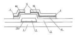
도 1에 도시하는 바와 같이, 본 발명의 실시예는, 베이스 기판(1)과, 이 베이스 기판(1)에 형성되어 있는 게이트 금속층(2)과 게이트 절연층(3)과 반도체층(4)과 오믹 접촉층(5)과 소스·드레인 금속층(6)과 패시베이션층(7)과 화소 전극(8)을 구비하는 어레이 기판을 제공한다. 게이트 금속층(2)과 베이스 기판(1) 사이에 제1 격리 버퍼층(21)이 형성되고, 오믹 접촉층(5)과 소스·드레인 금속층(6) 사이에 제2 격리 버퍼층(61)이 형성되어 있다.1, an embodiment of the present invention includes a
베이스 기판(1)은 유리 기판, 혹은 석영 기판일 수 있지만, 이들에 한정되지 않는다.The
게이트 금속층(2)과 소스·드레인 금속층(6)으로서, 본 실시예에서는 금속 Cu를 예로 들고 있지만, 다른 적절한 금속이나 합금 재료를 채용해도 좋다.As the
게이트 절연층(3)으로서는, SixNy(질화규소), 혹은, SixOy(산화규소) 등의 실리콘계 재료를 채용할 수 있지만, 이들에 한정되지 않는다.As the
반도체층(4)과 오믹 접촉층(5)을 조합하여 활성층이 형성된다. 반도체층(4)은 a-Si(아몰퍼스 실리콘) 재료에 의해 제조될 수 있으며, 오믹 접촉층(5)은, N+a-Si(도프 아몰퍼스 실리콘) 재료에 의해 제조될 수 있다.The active layer is formed by combining the
패시베이션층(7)으로서는, SixNy, 또는 SixOy 등의 실리콘계 재료, 혹은, 유기 수지 재료를 채용할 수 있다.As the
화소 전극(8)으로서는, ITO(산화인듐주석), 혹은 IZO(산화인듐아연) 등의 투명 도전 재료를 채용할 수 있다.As the
상기 제1 격리 버퍼층(21)과 상기 제2 격리 버퍼층(61) 중 적어도 한쪽이, MoOx에 의해 제조될 수 있다.At least one of the first
또한, 본 실시예에는, 도 1에 도시하는 어레이 기판(100)의 제조 방법도 제공한다.The present embodiment also provides a method of manufacturing the
도 2a 내지 도 2d에 도시하는 바와 같이, 상기 어레이 기판(100)의 제조 방법에는 이하와 같은 단계가 구비된다.As shown in FIGS. 2A to 2D, the method of manufacturing the
S11: 베이스 기판(1)에, MoOx 박막과 Cu 금속 박막을 순차적으로 증착하고, 패터닝 공정에 의해 제1 격리 버퍼층(21)과 게이트 금속층(2)의 패턴을 형성한다(도 2a 참조).S11: A MoOx thin film and a Cu metal thin film are sequentially deposited on the
제1 격리 버퍼층(21)의 패턴과, 게이트 금속층(2)의 패턴은, 어레이 기판의 TFT 구조 중에서, 상하 방향에서 대응하고, 패턴이 일치하고 있는 것을 유지한다.The pattern of the first
예를 들어, 베이스 기판(1)에 MoOx 박막을 증착하는 방법으로서, 이하와 같은 실현 방법 중 하나를 채용할 수 있다.For example, as a method of depositing a MoOx thin film on the
방법 A: 스퍼터링 공정에 의해, 혼합된 Ar(아르곤)과 O2를 이용하여, 금속 Mo 타깃재에 대하여 스퍼터링를 행하고, 단일층의 MoOx 박막을 형성하도록 한다.Method A: Sputtering is performed on a metal Mo target material by using a mixed Ar (argon) and O2 by a sputtering process to form a single layer of MoOx thin film.
방법 B: 스퍼터링 공정에 의해, 우선, 순수 Ar를 이용하여 Mo 타깃재에 대하여 스퍼터링를 행하고, 그 후에, 혼합된 Ar(아르곤)과 O2를 이용하여, 금속 Mo 타깃재에 대하여 두번째의 스퍼터링를 행하여, Mo 금속층과 MoOx 박막을 동시에 포함하는 2층 구조를 실현하도록 하고, 이에 의해, 저항을 저감함과 함께, 격리 버퍼층의 점착성을 높이는 것을 실현한다.Method B: Sputtering is performed on the Mo target material using pure Ar by a sputtering process, and then a second sputtering is performed on the metal Mo target material using mixed Ar (argon) and O2 , A two-layer structure including the Mo metal layer and the MoOx thin film at the same time is achieved, thereby realizing reduction in resistance and improvement in stickiness of the isolating buffer layer.
방법 C: 스퍼터링 공정에 의해, 기판(1)에 금속 Mo 박막을 형성하고 나서, 퍼니스(Furnace), 베이크 오븐(bake oven), RTP(Rapid Thermal Processing, 급속 가열 처리), RTA(Rapid Thermal Annealing, 고속 열 어닐링), CVD 또는 PVD(Physical Vapor Deposition, 물리 증착법) 등의 설비로, 산소 리치의 분위기에서 열처리를 행함으로써, MoOx막을 형성한다.Method C: A metal Mo thin film is formed on the
방법 D: 스퍼터링 공정에 의해, 베이스 기판(1)에 금속 Mo 박막을 형성하고, 플라즈마(Plasma) 설비 내에서, 산소(O2은 N2O)의 분위기에서 플라즈마 처리를 행하여, MoOx막을 형성한다.Method D: A metallic Mo thin film is formed on the
전술한 방법 A 및 방법 B의 실현 공정에서, Ar와 O2의 혼합 기체 중, O2가 차지하는 비율(체적 비율)은, 50% 이하인 것이 바람직하다.In the process of realizing the above-mentioned Method A and Method B, Ar and O2 ratio of the mixed gas, the O2 occupy the (volume ratio) is preferably not more than 50%.
상기 방법 C 및 방법 D의 실현 공정에서, 열처리를 행할 때, 혹은 플라즈마 처리를 행할 때에, 공정의 온도를 200℃ 내지 700℃로 제어할 수 있다.In the realization process of the method C and the method D, the temperature of the process can be controlled to 200 ° C to 700 ° C when the heat treatment is performed or the plasma treatment is performed.
S12: 게이트 금속층(2)이 형성되어 있는 베이스 기판(1)에, 게이트 절연층 재료, 반도체층 재료 및 오믹 접촉층 재료를 증착하고, 패터닝 공정에 의해, 게이트 절연층(3), 반도체층(4) 및 오믹 접촉층(5)의 패턴을 형성한다(도 2b 참조).S12: A gate insulating layer material, a semiconductor layer material, and an ohmic contact layer material are deposited on the
S13: 오믹 접촉층(5)이 형성되어 있는 베이스 기판(1)에 MoOx 박막과 Cu 금속 박막을 증착하고, 패터닝 공정에 의해, 제2 격리 버퍼층(61)과 소스·드레인 금속층(6)의 패턴을 형성한다(도 2c 참조).S13: a MoOx thin film and a Cu metal thin film are deposited on the
제2 격리 버퍼층(61)의 패턴과, 소스·드레인 금속층(6)의 패턴은, 어레이 기판의 TFT 구조에서, 상하 방향에서 대응하고, 패턴이 일치하고 있는 것을 유지한다.The pattern of the second
이 단계에서, MoOx 박막층을 형성하는 방법과, 단계 S11에 기재된 실현 방법은 마찬가지이므로, 여기에서는 설명을 생략한다.In this step, the method of forming the MoO x thin film layer and the method of realization described in step S11 are the same, and a description thereof will be omitted here.
S14: 소스·드레인 금속층(6)이 형성되어 있는 베이스 기판(1)에, 패시베이션층 재료를 증착하고, 패터닝 공정에 의해, 패시베이션층(7)의 패턴을 형성한다(도 2d 참조).S14: A passivation layer material is deposited on the
패시베이션층(7)으로서, SixNy, 및/또는 SixOy를 채용하는 경우, 막층이 너무 두껍게 증착되어서 막층의 치밀성에 문제가 발생하고, 또한 막층이 탈락하는 것을 회피할 수 있도록, 패시베이션층(7)의 두께를 1000Å 내지 6000Å로 한다. 패시베이션층(7)으로서, 유기 수지를 채용하는 경우, 여기에서, 비교적 큰 패시베이션층(7)을 채용함으로써, 화소 전극과 신호 전극 사이의 결합 용량을 저감시킬 수 있으므로, 패시베이션층(7)의 두께를 10000Å 내지 40000Å로 하고, 이에 의해, 화소 전극의 누설 전류 및 신호 전극에 대한 크로스 토크를 감소시킬 수 있다.In the case where SixNy and / or SixOy is employed as the
S15: 패시베이션층(7)이 형성되어 있는 베이스 기판(1)에, 화소 전극 재료를 증착하고, 패터닝 공정에 의해, 화소 전극(8)의 패턴을 형성한다(도 1 참조).S15: A pixel electrode material is deposited on the
본 실시예 및 다음의 실시예에서 설명되는 패터닝 공정에는, 포토레지스트 도포, 프리 베이킹, 마스크에 대한 노광·현상, 에칭 및 박리 등의 공정이 포함된다.The patterning process described in this embodiment and the following embodiments includes processes such as photoresist coating, prebaking, exposure and development to a mask, etching and peeling.
상기 어레이 기판(100)을 제조하는 공정의 프로세스는, 5회 마스크 공정을 예로 들어, 본 발명이 제공한 기술안에 대하여 설명한 것으로, 본 발명이 제공한 기술안은 4회 마스크 공정에서도 적용할 수 있고, 이 경우, 하프 노광 공정에 의해, 전술한 단계 S12 및 S13을 동일한 1회의 마스크 노광 공정에서 완성하면 좋다. 여기에서, 구체적인 공정에 관한 설명은 생략한다.The process of manufacturing the
본 발명의 실시예에 제공된 어레이 기판 및 그 제조 방법은, MoOx를 격리 버퍼층을 제조하는 재료로서 이용하여, 격리 버퍼층을 실현하는 새로운 방법을 제공한다. 또한, 산화몰리브덴을 포함하는 격리 버퍼층은, TFT 구조에 있어서, 금속 전극층의 금속 이온이, 활성층에 사용되는, 예를 들어 실리콘계 박막층으로 확산되는 것을 유효하게 방지할 수 있을 뿐만 아니라, 금속 전극층과 베이스 기판 사이의 점착력도 높일 수 있다.The array substrate and the manufacturing method thereof provided in the embodiment of the present invention provide a new method of realizing an isolation buffer layer by using MoOx as a material for manufacturing an isolation buffer layer. In addition, the isolation buffer layer containing molybdenum oxide can effectively prevent metal ions in the metal electrode layer from being diffused into, for example, a silicon-based thin film layer used in the active layer in the TFT structure, The adhesion between the substrates can also be increased.
[실시예 2][Example 2]
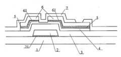
본 실시예는, 실시예 1에 의해 제공된 어레이 기판(100)에 대하여 더 개진하여, 다른 어레이 기판(200)의 구조를 제공한다.This embodiment is further advanced to the
도 3에 도시하는 바와 같이, 본 실시예는, 베이스 기판(1)과, 이 베이스 기판(1)에 형성되어 있는 게이트 금속층(2)과 게이트 절연층(3)과 반도체층(4)과 오믹 접촉층(5)과 소스·드레인 금속층(6)과 패시베이션층(7)과 화소 전극(8)을 구비하는 다른 어레이 기판(200)을 제공한다. 게이트 금속층(2)과 베이스 기판(1) 사이에, 제1 격리 버퍼층(21)이 형성되고, 오믹 접촉층(5)과 소스·드레인 금속층(6) 사이에, 제2 격리 버퍼층(61)이 형성되어 있다.3, the present embodiment is a semiconductor device including a
상기 금속층(2)과 게이트 절연층(3) 사이에는, 제3 격리 버퍼층(22)이 더 형성되어 있다.A third
본 실시예에서, 상기 금속층(2)과 소스·드레인 금속층(6)에는 금속 Cu를 채용하고 있지만, 다른 금속을 채용하여도 좋다.In the present embodiment, metal Cu is used for the
상기 제1 격리 버퍼층(21), 및/또는, 상기 제2 격리 버퍼층(61)은 MoOx에 의해 제조될 수 있다. 상기 제3 격리 버퍼층(22)은 금속 Mo 혹은 MoOx에 의해 제조될 수 있다.The first
본 실시예에서, 도 3에 도시하는 바와 같은 어레이 기판(200)의 제조 방법도 제공한다. 상기 방법의 구체적인 실현은, 도 1에 도시하는 바와 같은 어레이 기판(100)의 제조 공정과 유사하지만, 단계 S11에서, 베이스 기판(1)에 MoOx 박막과 Cu 금속 박막 및 금속 Mo 혹은 MoOx 박막을 순차적으로 증착하고, 패터닝 공정에 의해 제1 격리 버퍼층(21), 게이트 금속층(2) 및 제3 격리 버퍼층(22)의 패턴을 형성하는 것에 차이점이 있다.In this embodiment, a method of manufacturing the
제1 격리 버퍼층(21), 게이트 금속층(2) 및 제3 격리 버퍼층(22)의 패턴은, 어레이 기판 TFT 구조에서, 상하 방향에서 대응하고, 패턴이 일치하고 있는 것을 유지하고 있다.The patterns of the first isolating
본 실시예에 제공되는 어레이 기판 및 그 제조 방법은, 실시예 1에 더하여, 게이트 금속층과 게이트 절연층 사이에 한 층의 격리 버퍼층을 더 형성함으로써, 게이트 금속층과 게이트 절연층 사이의 점착력을 더 높여, 게이트 금속층과 게이트 절연층의 박리를 방지하면서, 게이트 금속층에서의 Cu 이온이 게이트 절연층으로 확산되는 것을 방지한다.The array substrate and the manufacturing method thereof provided in this embodiment can further improve adhesion between the gate metal layer and the gate insulating layer by further forming one insulating buffer layer between the gate metal layer and the gate insulating layer , Thereby preventing Cu ion in the gate metal layer from diffusing into the gate insulating layer while preventing peeling of the gate metal layer and the gate insulating layer.
[실시예 3][Example 3]
본 실시예는, 실시예 1에 의해 제공되는 어레이 기판(100)에 대하여 더 개진하여, 또 다른 어레이 기판(300)의 구조를 제공한다.This embodiment is further advanced to the
도 4에 도시하는 바와 같이, 본 실시예는, 베이스 기판(1)과, 이 베이스 기판(1)에 형성되어 있는 게이트 금속층(2)과 게이트 절연층(3)과 반도체층(4)과 오믹 접촉층(5)과 소스·드레인 금속층(6)과 패시베이션층(7)과 화소 전극(8)을 구비하는 또 다른 어레이 기판(300)을 제공한다. 게이트 금속층(2)과 베이스 기판(1) 사이에, 제1 격리 버퍼층(21)이 형성되고, 오믹 접촉층(5)과 소스·드레인 금속층(6) 사이에, 제2 격리 버퍼층(61)이 형성되고, 소스·드레인 금속층(6)과 패시베이션층(7) 사이에는 제4 격리 버퍼층(62)이 형성되어 있다.4, the present embodiment is a semiconductor device including a
본 실시예에서, 상기 게이트 금속층(2)과 소스·드레인 금속층(6)에는 금속 Cu를 채용하고 있지만, 이에 한정되지 않는다.In this embodiment, metal Cu is used for the
상기 제1 격리 버퍼층(21), 및/또는, 상기 제2 격리 버퍼층(61)은, MoOx에 의해 제조될 수 있고, 상기 제4 격리 버퍼층(62)은, 금속 Mo 혹은 MoOx에 의해 제조될 수 있다.The first
본 실시예에서, 도 4에 도시하는 바와 같은 어레이 기판(300)의 제조 방법도 제공한다. 상기 방법에서의 구체적인 실현은, 도 1에 도시하는 바와 같은 어레이 기판(100)의 제조 공정에 유사하지만, 단계 S13에서, 오믹 접촉층(5)이 형성되어 있는 기판에, MoOx 박막과 Cu 금속 박막 및 금속 Mo 혹은 MoOx 박막을 순차적으로 증착하고, 패터닝 공정에 의해, 제2 격리 버퍼층(61), 소스·드레인 금속층(6) 및 제4 격리 버퍼층(62)의 패턴을 형성하는 것에 차이점이 있다.In this embodiment, a method of manufacturing the
제2 격리 버퍼층(61), 소스·드레인 금속층(6) 및 제4 격리 버퍼층(62)의 패턴은, 어레이 기판 TFT 구조에서, 상하 방향에서 대응하고, 패턴이 일치하고 있는 것을 유지하고 있다.The patterns of the second
본 실시예에 제공되는 어레이 기판 및 그 제조 방법은, 실시예 1에 더하여, 소스·드레인 금속층과 패시베이션층 사이에 한 층의 격리 버퍼층을 더 형성함으로써, 소스·드레인 금속층과 패시베이션층 사이의 점착력을 높이어, 소스·드레인 금속층과 패시베이션층의 이탈을 방지함과 함께, 소스·드레인 금속층에서의 Cu와 화소 전극 사이의 접촉 저항을 유효하게 개선하여, Cu 금속이 산화되는 것을 방지한다.The array substrate and the manufacturing method thereof provided in the present embodiment are characterized in that in addition to the first embodiment, one layer of an isolation buffer layer is further formed between the source / drain metal layer and the passivation layer to improve the adhesion between the source / drain metal layer and the passivation layer Drain metal layer and the passivation layer, and effectively improves the contact resistance between Cu and the pixel electrode in the source / drain metal layer, thereby preventing the Cu metal from being oxidized.
[실시예 4][Example 4]
본 실시예에서, 상기 실시예 2에 따른 기술안과, 실시예 3에 따른 기술안을 결합하여, 새로운 어레이 기판을 제공한다.In this embodiment, a new array substrate is provided by combining the technology according to the second embodiment and the technology according to the third embodiment.
도 5에 도시하는 바와 같이, 본 실시예는, 베이스 기판(1)과, 이 베이스 기판(1)에 형성되어 있는 게이트 금속층(2)과 게이트 절연층(3)과 반도체층(4)과 오믹 접촉층(5)과 소스·드레인 금속층(6)과 패시베이션층(7)과 화소 전극(8)을 구비하는 또 다른 어레이 기판(400)을 제공한다. 게이트 금속층(2)과 베이스 기판(1) 사이에, 제1 격리 버퍼층(21)이 형성되고, 오믹 접촉층(5)과 소스·드레인 금속층(6) 사이에, 제2 격리 버퍼층(61)이 형성되어 있다. 또한, 상기 게이트 금속층(2)과 게이트 절연층(3) 사이에 제3 격리 버퍼층(22)이 형성되고, 소스·드레인 금속층(6)과 패시베이션층(7) 사이에 제4 격리 버퍼층(62)이 형성되어 있다.5, the present embodiment is a semiconductor device including a
본 실시예에서, 상기 게이트 금속층(2)과 소스·드레인 금속층(6)에는 금속 Cu를 채용하고 있지만, 이에 한정되지 않는다.In this embodiment, metal Cu is used for the
상기 제1 격리 버퍼층(21), 및/또는, 상기 제2 격리 버퍼층(61)은, MoOx에 의해 제조될 수 있으며, 상기 제3 격리 버퍼층(22), 및/또는, 상기 제4 격리 버퍼층(62)은 금속 Mo 혹은 MoOx에 의해 제조될 수 있다.The first
도 5에 도시되는 어레이 기판(400)의 제조 방법은, 실시예 2와 실시예 3에 제공된 어레이 기판(200,300)의 제조 방법을 결합함으로써 얻어지므로, 여기에서는 설명을 생략한다.The manufacturing method of the
본 실시예에 따른 어레이 기판 및 그 제조 방법은, 실시예 1에 더하여, 게이트 금속층과 게이트 절연층 사이에 한 층의 제3 격리 버퍼층을 더 형성하고, 소스·드레인 금속층과 패시베이션층 사이에 제4 격리 버퍼층을 형성함으로써, TFT 구조에서의 각 층의 사이의 점착력을 보다 향상시켜, 각 층의 사이에 이탈 현상이 발생하는 것을 방지함과 함께, 게이트 금속층에서의 Cu 이온이, 인접하는 층의 구조로 확산하는 것을 유효하게 방지하고, 소스·드레인 금속층에서의 Cu와 화소 전극 사이의 접촉 저항을 개선하여, Cu 금속이 산화되는 것을 방지할 수 있다.The array substrate according to the present embodiment and its manufacturing method are characterized in that, in addition to
실시예 1 내지 실시예 4에서는, 모두 보텀 게이트형의 TFT 구조를 예로 들어, 본 발명이 새롭게 제공한 어레이 기판 구조를 설명하였다. 그러나, 본 발명에 제공된 기술안은, 보텀 게이트형의 TFT 구조의 어레이 기판에 적용하는 것에 한정되지 않고, 톱 게이트형, 혹은 더블 게이트형 등의 TFT 구조의 어레이 기판에도 적용한다.In
이하, 본 발명에 제공되는 격리 버퍼층을 이용하여 실현하는 톱 게이트형의 TFT 구조에 대하여 간단하게 설명한다.Hereinafter, a top gate type TFT structure realized by using the isolation buffer layer provided in the present invention will be briefly described.
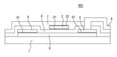
[실시예 5][Example 5]
도 6에 도시하는 바와 같이, 톱 게이트형의 TFT 어레이 기판(500)의 구조에 있어서, 베이스 기판(1)에, 활성층(9)과, 소스·드레인 금속층(6)과, 게이트 절연층(3)과, 게이트 금속층(2)과, 패시베이션층(7)과, 화소 전극(8)을 순차적으로 형성한다. 활성층(9)은 반도체층만을 포함하는 단일층의 구조이어도 좋고, 반도체층과 오믹 접촉층을 포함하는 2층의 구조이어도 좋다. 도 6에 도시되는 TFT 어레이 기판(500)의 구조에 있어서, 활성층(9)의 구체적인 실현 방법에 대하여 구별하여 도시하지 않았지만, 일 층의 구조에 한정되지 않는다.6, in the structure of the top gate type
상기 톱 게이트형의 TFT 어레이 기판(500)의 구조에 있어서, 게이트 금속층(2)과 게이트 절연층(3) 사이에 제1 격리 버퍼층(21)이 형성되고, 활성층(9)과 소스·드레인 금속층(6) 사이에 제2 격리 버퍼층(61)이 형성되어 있다. 또한, 상기 제1 격리 버퍼층(21), 및/또는 제2 격리 버퍼층(61)은, MoOx에 의해 제조될 수 있다.In the structure of the top gate type
또한, 도 6에 도시되는 어레이 기판(500)을 제조하는 공정에는, 베이스 기판(1)에, 활성층(9)과, 소스·드레인 금속층(6)과, 게이트 절연층(3) 및 게이트 금속층(2), 패시베이션층(7) 및 화소 전극(8)을 순차적으로 형성하는 단계가 포함된다.6, an
소스·드레인 금속층(6)을 제조하는 동시에, 제2 격리 버퍼층(61)을 제조한다. 구체적으로는, 활성층(9)이 형성되어 있는 기판에 산화몰리브덴 박막과 소스·드레인 금속층을 형성하고, 패터닝 공정에 의해, 동일한 패턴을 갖는 제2 격리 버퍼층(61)과 소스·드레인 금속층(6)의 패턴을 형성한다.The source /
게이트 금속층(2)을 제조하는 동시에, 제1 격리 버퍼층(21)을 제조한다. 구체적으로는, 게이트 절연층(3)이 형성되어 있는 기판에 산화몰리브덴 박막과 게이트 금속 박막을 순차적으로 증착하고, 패터닝 공정에 의해, 동일한 패턴을 갖는 제1 격리 버퍼층(21)과 게이트 금속층(2)의 패턴을 형성한다.The first
상기 어레이 기판(500)을 제조하는 공정에서, MoOx 박막을 증착 형성하는 공정은 실시예 1과 유사하므로, 여기에서는 설명을 생략한다.In the process of manufacturing the
본 발명의 실시예에 따른 어레이 기판 및 그 제조 방법은, MoOx를 격리 버퍼층을 제조하는 재료로서 이용하여, 격리 버퍼층을 실현하는 새로운 방법을 제공한다. 또한, 산화몰리브덴을 포함하는 격리 버퍼층은, TFT 구조에서의 금속 전극층의 금속 이온이, 활성층에 사용되는, 예를 들어 실리콘계 박막층으로 확산되는 것을 유효하게 방지할 수 있을 뿐만 아니라, 금속 전극층과, 그에 인접하는 층과의 사이의 점착력을 증가시켜, 금속 전극층에 이탈 현상이 발생하는 것을 방지할 수도 있다.An array substrate and a manufacturing method thereof according to an embodiment of the present invention provide a new method of realizing an isolation buffer layer by using MoOx as a material for manufacturing an isolation buffer layer. Further, the isolating buffer layer containing molybdenum oxide can effectively prevent the metal ions of the metal electrode layer in the TFT structure from diffusing into, for example, a silicon-based thin film layer used in the active layer, It is possible to increase the adhesive force with the adjacent layer and to prevent the occurrence of the separation phenomenon in the metal electrode layer.
[실시예 6][Example 6]
본 실시예는, 실시예 5에 제공되는 어레이 기판(500)에 대하여 더 개진하여, 다른 톱 게이트형의 TFT 어레이 기판의 구조를 제공한다.This embodiment is further provided for the
도 7에 도시하는 바와 같이, 본 실시예에 따른 어레이 기판(600)은, 실시예 5에 제공된 어레이 기판(500)의 구조를 구비하는 이외에, 게이트 금속층(2)과 패시베이션층(7) 사이에, 제3 격리 버퍼층(22)이 더 형성되고, 이 제3 격리 버퍼층(22)은, 금속 Mo 혹은 MoOx에 의해 제조될 수 있다.7, the
또한, 도 7에 도시되는 어레이 기판(600)을 제조하는 공정에서, 제1 격리 버퍼층(21)과 제3 격리 버퍼층(22)은 모두 게이트 금속층(2)과 함께 동일한 1회의 마스크(mask) 공정에 의해 제조될 수 있고, 구체적으로는, 게이트 절연층(3)이 형성되어 있는 기판에, 산화몰리브덴 박막과, 게이트 금속 박막과, 금속 몰리브덴 혹은 산화몰리브덴 박막을 순차적으로 증착하여, 패터닝 공정에 의해, 제1 격리 버퍼층(21)과, 상기 게이트 금속층(2)과, 제3 격리 버퍼층(22)의 패턴을 형성한다.7, both the first
본 발명의 실시예에 제공되는 어레이 기판 및 그 제조 방법은, MoOx를 격리 버퍼층을 제조하는 재료로서 이용하여, 격리 버퍼층을 실현하는 새로운 방법을 제공한다. 또한, 산화몰리브덴을 포함하는 격리 버퍼층은, TFT 구조에서의 금속 전극층의 금속 이온이, 활성층에 사용되는, 예를 들어 실리콘계 박막층으로 확산되는 것을 유효하게 방지할 수 있을 뿐만 아니라, 금속 전극층과, 그에 인접하는 층 사이의 점착력을 증가시켜, 금속 전극층에 이탈 현상이 발생하는 것을 방지할 수도 있다.The array substrate and the manufacturing method thereof provided in the embodiment of the present invention provide a new method of realizing an isolation buffer layer by using MoOx as a material for manufacturing an isolation buffer layer. Further, the isolating buffer layer containing molybdenum oxide can effectively prevent the metal ions of the metal electrode layer in the TFT structure from diffusing into, for example, a silicon-based thin film layer used in the active layer, It is possible to increase the adhesive force between adjacent layers and prevent the occurrence of separation phenomenon in the metal electrode layer.
[실시예 7][Example 7]
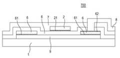
본 실시예는, 실시예 5에 제공되는 어레이 기판(500)에 대하여 더 개진하여, 또 다른 톱 게이트형의 TFT 어레이 기판의 구조를 제공한다.This embodiment is further provided for the
구체적으로는, 도 8에 도시하는 바와 같이, 본 실시예에 따른 어레이 기판(700)은, 실시예 5에 제공되는 어레이 기판(500)의 구조를 구비하는 이외에, 게이트 절연층(3)과 소스·드레인 금속층(6) 사이에, 제4 격리 버퍼층(62)이 형성되고, 이 제4 격리 버퍼층(62)은 금속 몰리브덴 혹은 산화몰리브덴에 의해 제조될 수 있다.Specifically, as shown in FIG. 8, the
또한, 도 8에 도시되는 어레이 기판(700)을 제조하는 공정에 있어서, 제2 격리 버퍼층(61)과 제4 격리 버퍼층(62)은, 모두 소스·드레인 금속층(6)과 함께 동일한 1회의 마스크 공정에 의해 제조될 수 있고, 구체적으로는, 활성층(9)이 형성되어 있는 베이스 기판(1)에, 산화몰리브덴 박막과, 소스·드레인 금속 박막과, 금속 몰리브덴 혹은 산화몰리브덴 박막을 형성하고, 패터닝 공정에 의해, 마찬가지인 패턴을 갖는 제2 격리 버퍼층(61), 상기 소스·드레인 금속층(6) 및 제4 격리 버퍼층(62)의 패턴을 형성한다.8, the second
본 실시예에 제공되는 어레이 기판 및 그 제조 방법은, 소스·드레인 금속층과 게이트 절연층 사이의 점착력을 높이어, 소스·드레인 금속층과 게이트 절연층의 이탈을 방지함과 함께, 소스·드레인 금속층에서의 Cu와 화소 전극 사이의 접촉 저항을 유효하게 개선하여, Cu 금속이 산화되는 것을 방지할 수 있다.The array substrate and the manufacturing method thereof provided in this embodiment increase the adhesion between the source / drain metal layer and the gate insulating layer to prevent the source / drain metal layer and the gate insulating layer from separating from each other, The contact resistance between Cu and the pixel electrode can be effectively improved and the Cu metal can be prevented from being oxidized.
[실시예 8][Example 8]
본 실시예는, 전술한 실시예 6에 따른 기술안과, 실시예 7에 따른 기술안을 결합하여, 새로운 어레이 기판 구조를 제공한다.This embodiment combines the technology according to the above-described
도 9에 도시하는 바와 같이, 본 실시예에 제공되는 어레이 기판(800)은, 실시예 5에 제공된 어레이 기판(500)의 구조를 구비하는 이외에, 게이트 금속층(2)과 패시베이션층(7) 사이에, 제3 격리 버퍼층(22)이 형성되고, 게이트 절연층(3)과, 소스·드레인 금속층(6) 사이에, 제4 격리 버퍼층(62)이 형성되고, 상기 제3 격리 버퍼층(22)과 제4 격리 버퍼층(62)은, 금속 몰리브덴 혹은 산화몰리브덴에 의해 제조될 수 있다.9, the
도 9에 도시하는 어레이 기판(800)을 제조하는 방법은, 실시예 6과 실시예 7에 제공되는 어레이 기판(600,700)의 제조 방법을 결합할 수 있으므로, 여기에서는 설명을 생략한다.The method of manufacturing the
본 실시예에 제공되는 어레이 기판 및 그 제조 방법은, TFT 구조에서의 각 층의 사이의 점착력을 보다 향상시킬 수 있어, 각 층의 사이에 이탈 현상이 발생하는 것을 방지함과 함께, 게이트 금속층에서의 Cu 이온이 인접하는 층의 구조로 확산되는 것을 유효하게 방지하고, 또한 소스·드레인 금속층에서의 Cu와 화소 전극 사이의 접촉 저항을 유효하게 개선하여, Cu 금속이 산화되는 것을 방지할 수 있다.The array substrate and the manufacturing method thereof provided in this embodiment can further improve adhesion between the respective layers in the TFT structure and prevent the occurrence of separation phenomenon between the respective layers, Can effectively prevent Cu ions in the source / drain metal layer from diffusing into the structure of the adjacent layer, and effectively improve the contact resistance between Cu and the pixel electrode in the source / drain metal layer, thereby preventing Cu metal from being oxidized.
본 발명은 대향하여 설치된 컬러 필터 기판과 어레이 기판 및 컬러 필터와 어레이 기판 사이에 개재되어 있는 액정층을 구비한 액정 패널로서, 상기 어레이 기판은, 전술한 실시예에 제공되는 어레이 기판을 채용할 수 있는 액정 패널도 제공한다.The present invention is a liquid crystal panel including a color filter substrate and an array substrate opposed to each other, and a liquid crystal layer interposed between the color filter and the array substrate, wherein the array substrate can employ the array substrate provided in the above- A liquid crystal panel is also provided.
본 발명의 실시예는 전술한 실시예에 제공되는 어레이 기판을 채용하는 디스플레이도 제공한다.Embodiments of the present invention also provide a display employing the array substrate provided in the above-described embodiments.
전술한 디스플레이는, 액정 디스플레이에 한정되지 않고, OLED 디스플레이나 전자 북 등의 디스플레이이어도 좋다.The above-described display is not limited to a liquid crystal display, and may be a display such as an OLED display or an electronic book.
본 발명의 실시예에 따른 액정 패널과 디스플레이는, 전술한 실시예에서의 어레이 기판을 채용했으므로, 전술한 실시예에 설명된 기술 효과와 마찬가지의 효과를 발휘할 수 있다.Since the liquid crystal panel and the display according to the embodiment of the present invention employ the array substrate in the above-described embodiment, the same effect as the technical effect described in the above-described embodiment can be obtained.
본 발명의 실시예에 제공되는 기술안은 TFT 어레이 기판을 채용한 다종의 디스플레이에 적용될 뿐만 아니라, X선 측정 장치에도 적용된다.The technical idea provided in the embodiment of the present invention is applied not only to various kinds of displays employing a TFT array substrate but also to an X-ray measuring apparatus.
이상은 본 발명의 구체적인 실시예일 뿐이고, 본 발명의 보호 범위를 한정하는 것은 아니며, 당업자는 본 발명에 개시된 기술 범위 내에서, 용이하게 변화하거나 변경할 수 있는 것들은, 모두 본 발명의 보호 범위에 속한다. 이 때문에, 본 발명의 보호 범위는, 청구항의 보호 범위를 기준으로 하고 있다.Those skilled in the art will readily appreciate that various modifications, additions and substitutions are possible, without departing from the scope and spirit of the invention as disclosed in the accompanying claims. Therefore, the protection scope of the present invention is based on the protection scope of the claims.
1 기판
2 게이트 금속층
21 제1 격리 버퍼층
22 제3 격리 버퍼층
3 게이트 절연층
4 반도체층
5 오믹 접촉층
6 소스·드레인 금속층
61 제2 격리 버퍼층
62 제4 격리 버퍼층
7 패시베이션층
8 화소 전극
9 활성층1 substrate
2 gate metal layer
21 first isolation buffer layer
22 third isolating buffer layer
3 gate insulating layer
4 semiconductor layer
5 ohmic contact layer
6 source / drain metal layer
61 second isolating buffer layer
62 fourth isolating buffer layer
7 passivation layer
8 pixel electrode
9 active layer
Claims (17)
Translated fromKorean상기 게이트 금속층의 두께 방향에서의 적어도 일측에 격리 버퍼층이 형성되고, 및/또는 상기 소스·드레인 금속층의 두께 방향에서의 적어도 일측에 격리 버퍼층이 형성되고,
상기 어레이 기판은 보텀 게이트형의 구조를 채용하고, 상기 게이트 금속층과 상기 활성층 사이에 게이트 절연층이 더 형성되며,
상기 게이트 금속층의 적어도 일측에 형성되는 격리 버퍼층에는, 상기 게이트 금속층과 상기 베이스 기판 사이에 형성되는 제1 격리 버퍼층, 혹은 상기 게이트 금속층과 상기 베이스 기판 사이에 형성되는 제1 격리 버퍼층 및 상기 게이트 금속층과 상기 게이트 절연층 사이에 형성되는 제3 격리 버퍼층이 포함되고,
상기 제1 격리 버퍼층은 산화몰리브덴에 의해 제조되고, 상기 제3 격리 버퍼층은 금속 몰리브덴 또는 산화몰리브덴에 의해 제조되는 것을 특징으로 하는 어레이 기판.An array substrate comprising a base substrate, a gate metal layer formed on the base substrate, an active layer, and a source / drain metal layer,
An isolation buffer layer is formed on at least one side in the thickness direction of the gate metal layer and / or an isolation buffer layer is formed on at least one side in the thickness direction of the source / drain metal layer,
The array substrate adopts a bottom gate type structure, a gate insulating layer is further formed between the gate metal layer and the active layer,
A first isolation buffer layer formed between the gate metal layer and the base substrate or a first isolation buffer layer formed between the gate metal layer and the base substrate and a second isolation buffer layer formed between the gate metal layer and the base substrate, And a third isolation buffer layer formed between the gate insulation layers,
Wherein the first isolation buffer layer is made of molybdenum oxide and the third isolation buffer layer is made of metal molybdenum or molybdenum oxide.
상기 게이트 금속층의 두께 방향에서의 적어도 일측에 격리 버퍼층이 형성되고, 및/또는 상기 소스·드레인 금속층의 두께 방향에서의 적어도 일측에 격리 버퍼층이 형성되고,
상기 어레이 기판은 톱 게이트형의 구조를 채용하고, 상기 게이트 금속층과 상기 활성층 사이에 형성되는 게이트 절연층과, 상기 게이트 금속층 상에 형성되는 패시베이션층을 더 구비하고,
상기 게이트 금속층의 적어도 일측에 형성되는 격리 버퍼층에는, 상기 게이트 금속층과 상기 게이트 절연층 사이에 형성되는 제1 격리 버퍼층, 혹은 상기 게이트 금속층과 상기 게이트 절연층 사이에 형성되는 제1 격리 버퍼층 및 상기 게이트 금속층과 상기 패시베이션층 사이에 형성되는 제3 격리 버퍼층이 포함되고,
상기 제1 격리 버퍼층은 산화몰리브덴에 의해 제조되고, 상기 제3 격리 버퍼층은 금속 몰리브덴 또는 산화몰리브덴에 의해 제조되는 것을 특징으로 하는 어레이 기판.An array substrate comprising a base substrate, a gate metal layer formed on the base substrate, an active layer, and a source / drain metal layer,
An isolation buffer layer is formed on at least one side in the thickness direction of the gate metal layer and / or an isolation buffer layer is formed on at least one side in the thickness direction of the source / drain metal layer,
Wherein the array substrate has a top gate type structure and further includes a gate insulating layer formed between the gate metal layer and the active layer and a passivation layer formed on the gate metal layer,
A first isolation buffer layer formed between the gate metal layer and the gate insulation layer or a first isolation buffer layer formed between the gate metal layer and the gate insulation layer and a second isolation buffer layer formed between the gate metal layer and the gate insulation layer, And a third isolation buffer layer formed between the metal layer and the passivation layer,
Wherein the first isolation buffer layer is made of molybdenum oxide and the third isolation buffer layer is made of metal molybdenum or molybdenum oxide.
상기 게이트 금속층의 두께 방향에서의 적어도 일측에 격리 버퍼층이 형성되고, 및/또는 상기 소스·드레인 금속층의 두께 방향에서의 적어도 일측에 격리 버퍼층이 형성되고,
상기 어레이 기판은 보텀 게이트형의 구조를 채용하고, 상기 소스·드레인 금속층 상에 패시베이션층이 형성되고,
상기 소스·드레인 금속층의 적어도 일측에 형성되는 격리 버퍼층에는, 상기 활성층과 상기 소스·드레인 금속층 사이에 형성되고 산화몰리브덴에 의해 제조되는 제2 격리 버퍼층, 혹은 상기 활성층과 상기 소스·드레인 금속층 사이에 형성되고 산화몰리브덴에 의해 제조되는 제2 격리 버퍼층 및 상기 패시베이션층과 상기 소스·드레인 금속층 사이에 형성되는 제4 격리 버퍼층이 포함되고,
상기 제4 격리 버퍼층은 금속 몰리브덴 또는 산화몰리브덴에 의해 제조되는 것을 특징으로 하는 어레이 기판.An array substrate comprising a base substrate, a gate metal layer formed on the base substrate, an active layer, and a source / drain metal layer,
An isolation buffer layer is formed on at least one side in the thickness direction of the gate metal layer and / or an isolation buffer layer is formed on at least one side in the thickness direction of the source / drain metal layer,
Wherein the array substrate adopts a bottom gate type structure, a passivation layer is formed on the source / drain metal layer,
A second isolation buffer layer formed between the active layer and the source / drain metal layer and made of molybdenum oxide, or a second isolation buffer layer formed between the active layer and the source / drain metal layer in the isolation buffer layer formed on at least one side of the source / A second isolation buffer layer made of molybdenum oxide and a fourth isolation buffer layer formed between the passivation layer and the source / drain metal layer,
Wherein the fourth isolation buffer layer is made of metal molybdenum or molybdenum oxide.
상기 어레이 기판은 소스·드레인 금속층 상에 패시베이션층이 형성되고,
상기 소스·드레인 금속층의 적어도 일측에 형성되는 격리 버퍼층에는, 상기 활성층과 상기 소스·드레인 금속층 사이에 형성되고 산화몰리브덴에 의해 제조되는 제2 격리 버퍼층, 혹은 상기 활성층과 상기 소스·드레인 금속층 사이에 형성되고 산화몰리브덴에 의해 제조되는 제2 격리 버퍼층 및 상기 패시베이션층과 상기 소스·드레인 금속층 사이에 형성되는 제4 격리 버퍼층이 포함되고,
상기 제4 격리 버퍼층은 금속 몰리브덴 또는 산화몰리브덴에 의해 제조되는 것을 특징으로 하는 어레이 기판.The method according to claim 1,
The array substrate has a passivation layer formed on a source / drain metal layer,
A second isolation buffer layer formed between the active layer and the source / drain metal layer and made of molybdenum oxide, or a second isolation buffer layer formed between the active layer and the source / drain metal layer in the isolation buffer layer formed on at least one side of the source / A second isolation buffer layer made of molybdenum oxide and a fourth isolation buffer layer formed between the passivation layer and the source / drain metal layer,
Wherein the fourth isolation buffer layer is made of metal molybdenum or molybdenum oxide.
상기 게이트 금속층의 두께 방향에서의 적어도 일측에 격리 버퍼층이 형성되고, 및/또는 상기 소스·드레인 금속층의 두께 방향에서의 적어도 일측에 격리 버퍼층이 형성되고,
상기 어레이 기판은 톱 게이트형의 구조를 채용하고, 상기 게이트 금속층과 상기 소스·드레인 금속층 사이에 게이트 절연층이 형성되고,
상기 소스·드레인 금속층의 적어도 일측에 형성되는 격리 버퍼층에는, 상기 활성층과 상기 소스·드레인 금속층 사이에 형성되고 산화몰리브덴에 의해 제조되는 제2 격리 버퍼층, 혹은 상기 활성층과 상기 소스·드레인 금속층 사이에 형성되고 산화몰리브덴에 의해 제조되는 제2 격리 버퍼층 및 상기 게이트 절연층과 상기 소스·드레인 금속층 사이에 형성되는 제4 격리 버퍼층이 포함되고,
상기 제4 격리 버퍼층은 금속 몰리브덴 또는 산화몰리브덴에 의해 제조되는 것을 특징으로 하는 어레이 기판.An array substrate comprising a base substrate, a gate metal layer formed on the base substrate, an active layer, and a source / drain metal layer,
An isolation buffer layer is formed on at least one side in the thickness direction of the gate metal layer and / or an isolation buffer layer is formed on at least one side in the thickness direction of the source / drain metal layer,
The array substrate adopts a top gate type structure, a gate insulating layer is formed between the gate metal layer and the source / drain metal layer,
A second isolation buffer layer formed between the active layer and the source / drain metal layer and made of molybdenum oxide, or a second isolation buffer layer formed between the active layer and the source / drain metal layer in the isolation buffer layer formed on at least one side of the source / A second isolation buffer layer made of molybdenum oxide and a fourth isolation buffer layer formed between the gate insulation layer and the source / drain metal layer,
Wherein the fourth isolation buffer layer is made of metal molybdenum or molybdenum oxide.
상기 어레이 기판은 상기 게이트 금속층과 상기 소스·드레인 금속층 사이에 게이트 절연층이 형성되고,
상기 소스·드레인 금속층의 적어도 일측에 형성되는 격리 버퍼층에는, 상기 활성층과 상기 소스·드레인 금속층 사이에 형성되고 산화몰리브덴에 의해 제조되는 제2 격리 버퍼층, 혹은 상기 활성층과 상기 소스·드레인 금속층 사이에 형성되고 산화몰리브덴에 의해 제조되는 제2 격리 버퍼층 및 상기 게이트 절연층과 상기 소스·드레인 금속층 사이에 형성되는 제4 격리 버퍼층이 포함되고,
상기 제4 격리 버퍼층은 금속 몰리브덴 또는 산화몰리브덴에 의해 제조되는 것을 특징으로 하는 어레이 기판.3. The method of claim 2,
Wherein the array substrate has a gate insulating layer formed between the gate metal layer and the source / drain metal layer,
A second isolation buffer layer formed between the active layer and the source / drain metal layer and made of molybdenum oxide, or a second isolation buffer layer formed between the active layer and the source / drain metal layer in the isolation buffer layer formed on at least one side of the source / A second isolation buffer layer made of molybdenum oxide and a fourth isolation buffer layer formed between the gate insulation layer and the source / drain metal layer,
Wherein the fourth isolation buffer layer is made of metal molybdenum or molybdenum oxide.
상기 게이트 금속층과 소스·드레인 금속층 중 적어도 한쪽이 금속 Cu 혹은 Cu 합금에 의해 형성되는 것을 특징으로 하는 어레이 기판.7. The method according to any one of claims 1 to 6,
Wherein at least one of the gate metal layer and the source / drain metal layer is formed of a metal Cu or a Cu alloy.
상기 게이트 금속층의 적어도 일측에, 상기 게이트 금속층과 마찬가지의 패턴을 갖는 격리 버퍼층을 형성하는 단계, 및/또는 상기 소스·드레인 금속층의 적어도 일측에, 상기 소스·드레인 금속층과 마찬가지의 패턴을 갖는 격리 버퍼층을 형성하는 단계를 포함하고,
상기 격리 버퍼층은 산화몰리브덴에 의해 제조되는 어레이 기판의 제조 방법.7. A method of manufacturing an array substrate according to any one of claims 1 to 6, wherein a gate metal layer, an active layer, and a source / drain metal layer are formed on a base substrate,
A step of forming an isolation buffer layer having a pattern similar to that of the gate metal layer on at least one side of the gate metal layer and / or a step of forming, on at least one side of the source / drain metal layer, , ≪ / RTI >
Wherein the isolation buffer layer is made of molybdenum oxide.
게이트 금속층의 적어도 일측에, 상기 게이트 금속층과 마찬가지의 패턴을 갖는 격리 버퍼층을 형성하는 단계, 및/또는 소스·드레인 금속층의 적어도 일측에, 상기 소스·드레인 금속층과 마찬가지의 패턴을 갖는 격리 버퍼층을 형성하는 단계를 포함하고,
상기 어레이 기판은 보텀 게이트형의 구조를 채용하고,
상기 게이트 금속층의 적어도 일측에, 상기 게이트 금속층과 마찬가지인 패턴을 갖는 격리 버퍼층을 형성하는 단계는, 상기 베이스 기판에 산화몰리브덴 박막과 게이트 금속 박막을 순차적으로 증착하고, 패터닝 공정에 의해 제1 격리 버퍼층과 상기 게이트 금속층의 패턴을 형성하는 것을 특징으로 하는 어레이 기판의 제조 방법.7. A method of manufacturing an array substrate according to any one of claims 1, 3, and 4, wherein a gate metal layer, an active layer, and a source / drain metal layer are formed on a base substrate,
Forming an isolation buffer layer having a pattern similar to that of the gate metal layer on at least one side of the gate metal layer and / or forming an isolation buffer layer having a pattern similar to that of the source / drain metal layer on at least one side of the source / drain metal layer , ≪ / RTI >
The array substrate adopts a bottom gate type structure,
The step of forming an isolation buffer layer having a pattern similar to that of the gate metal layer on at least one side of the gate metal layer includes sequentially depositing a molybdenum oxide thin film and a gate metal thin film on the base substrate, And forming a pattern of the gate metal layer.
게이트 금속층의 적어도 일측에, 상기 게이트 금속층과 마찬가지의 패턴을 갖는 격리 버퍼층을 형성하는 단계, 및/또는 소스·드레인 금속층의 적어도 일측에, 상기 소스·드레인 금속층과 마찬가지의 패턴을 갖는 격리 버퍼층을 형성하는 단계를 포함하고,
상기 어레이 기판은 보텀 게이트형의 구조를 채용하고,
상기 게이트 금속층의 적어도 일측에, 상기 게이트 금속층과 마찬가지의 패턴을 갖는 격리 버퍼층을 형성하는 단계는, 상기 베이스 기판에 산화몰리브덴 박막, 게이트 금속 박막 및 금속 몰리브덴 박막 또는 산화몰리브덴 박막을 순차적으로 증착하고, 패터닝 공정에 의해 제1 격리 버퍼층, 상기 게이트 금속층 및 제3 격리 버퍼층의 패턴을 형성하는 것을 특징으로 하는 어레이 기판의 제조 방법.7. A method of manufacturing an array substrate according to any one of claims 1, 3, and 4, wherein a gate metal layer, an active layer, and a source / drain metal layer are formed on a base substrate,
Forming an isolation buffer layer having a pattern similar to that of the gate metal layer on at least one side of the gate metal layer and / or forming an isolation buffer layer having a pattern similar to that of the source / drain metal layer on at least one side of the source / drain metal layer , ≪ / RTI >
The array substrate adopts a bottom gate type structure,
The step of forming an isolation buffer layer having a pattern similar to that of the gate metal layer on at least one side of the gate metal layer includes sequentially depositing a molybdenum oxide thin film, a gate metal thin film, a metal molybdenum thin film, or a molybdenum oxide thin film on the base substrate, And patterning the first isolation buffer layer, the gate metal layer, and the third isolation buffer layer by a patterning process.
게이트 금속층의 적어도 일측에, 상기 게이트 금속층과 마찬가지의 패턴을 갖는 격리 버퍼층을 형성하는 단계, 및/또는 소스·드레인 금속층의 적어도 일측에, 상기 소스·드레인 금속층과 마찬가지의 패턴을 갖는 격리 버퍼층을 형성하는 단계를 포함하고,
상기 어레이 기판은 톱 게이트형의 구조를 채용하고,
상기 게이트 금속층의 적어도 일측에, 상기 게이트 금속층과 마찬가지의 패턴을 갖는 격리 버퍼층을 형성하는 단계는, 게이트 절연층이 형성되어 있는 상기 베이스 기판에 산화몰리브덴 박막과 게이트 금속 박막을 순차적으로 증착하고, 패터닝 공정에 의해 제1 격리 버퍼층과 상기 게이트 금속층의 패턴을 형성하는 것을 특징으로 하는 어레이 기판의 제조 방법.6. A method of manufacturing an array substrate according to any one of claims 2, 5, and 6, wherein a gate metal layer, an active layer, and a source / drain metal layer are formed on a base substrate,
Forming an isolation buffer layer having a pattern similar to that of the gate metal layer on at least one side of the gate metal layer and / or forming an isolation buffer layer having a pattern similar to that of the source / drain metal layer on at least one side of the source / drain metal layer , ≪ / RTI >
The array substrate adopts a top gate type structure,
The step of forming an isolation buffer layer having a pattern similar to that of the gate metal layer on at least one side of the gate metal layer includes sequentially depositing a molybdenum oxide thin film and a gate metal thin film on the base substrate on which the gate insulating layer is formed, And forming a pattern of the first isolation buffer layer and the gate metal layer.
게이트 금속층의 적어도 일측에, 상기 게이트 금속층과 마찬가지의 패턴을 갖는 격리 버퍼층을 형성하는 단계, 및/또는 소스·드레인 금속층의 적어도 일측에, 상기 소스·드레인 금속층과 마찬가지의 패턴을 갖는 격리 버퍼층을 형성하는 단계를 포함하고,
상기 어레이 기판은 톱 게이트형의 구조를 채용하고,
상기 게이트 금속층의 적어도 일측에, 상기 게이트 금속층과 마찬가지의 패턴을 갖는 격리 버퍼층을 형성하는 단계는, 게이트 절연층이 형성되어 있는 상기 베이스 기판에 산화몰리브덴 박막, 게이트 금속 박막, 및 금속 몰리브덴 박막 또는 산화몰리브덴 박막을 순차적으로 증착하고, 패터닝 공정에 의해 제1 격리 버퍼층, 상기 게이트 금속층 및 제3 격리 버퍼층의 패턴을 형성하는 것을 특징으로 하는 어레이 기판의 제조 방법.6. A method of manufacturing an array substrate according to any one of claims 2, 5, and 6, wherein a gate metal layer, an active layer, and a source / drain metal layer are formed on a base substrate,
Forming an isolation buffer layer having a pattern similar to that of the gate metal layer on at least one side of the gate metal layer and / or forming an isolation buffer layer having a pattern similar to that of the source / drain metal layer on at least one side of the source / drain metal layer , ≪ / RTI >
The array substrate adopts a top gate type structure,
The step of forming an isolation buffer layer having a pattern similar to that of the gate metal layer on at least one side of the gate metal layer may include the steps of forming a molybdenum oxide thin film, a gate metal thin film, a metal molybdenum thin film, And a pattern of a first isolation buffer layer, a gate metal layer, and a third isolation buffer layer are formed by a patterning process.
상기 소스·드레인 금속층의 적어도 일측에, 상기 소스·드레인 금속층과 마찬가지의 패턴을 갖는 격리 버퍼층을 형성하는 단계는, 상기 활성층이 형성되어 있는 상기 베이스 기판에 산화몰리브덴 박막과 소스·드레인 금속 박막을 형성하고, 패터닝 공정에 의해, 제2 격리 버퍼층과 상기 소스·드레인 금속층의 패턴을 형성하는 것을 특징으로 하는 어레이 기판의 제조 방법.9. The method of claim 8,
The step of forming an isolation buffer layer having a pattern similar to that of the source / drain metal layer on at least one side of the source / drain metal layer includes forming a molybdenum oxide thin film and a source / drain metal thin film on the base substrate on which the active layer is formed And patterning the second isolation buffer layer and the source / drain metal layer by a patterning process.
상기 소스·드레인 금속층의 적어도 일측에, 상기 소스·드레인 금속층과 마찬가지의 패턴을 갖는 격리 버퍼층을 형성하는 단계는, 상기 활성층이 형성되어 있는 상기 베이스 기판에 산화몰리브덴 박막, 소스·드레인 금속 박막, 및 금속 몰리브덴 박막 또는 산화몰리브덴 박막을 형성하고, 패터닝 공정에 의해 제2 격리 버퍼층, 상기 소스·드레인 금속층의 패턴 및 제4 격리 버퍼층의 패턴을 형성하는 것을 특징으로 하는 어레이 기판의 제조 방법.9. The method of claim 8,
The step of forming an isolation buffer layer having a pattern similar to that of the source / drain metal layer on at least one side of the source / drain metal layer includes the steps of: forming a molybdenum oxide thin film, a source / drain metal thin film, A metal molybdenum thin film or a molybdenum oxide thin film is formed on the substrate, and a pattern of the second isolation buffer layer, the pattern of the source / drain metal layer, and the pattern of the fourth isolation buffer layer is formed by the patterning process.
a: 스퍼터링 공정에 의해, 혼합된 Ar(아르곤)과 O2를 이용하여, 금속 Mo 타깃재에 대하여 스퍼터링를 행하여, 단일층의 MoOx 박막을 형성하도록 하는 단계와,
b: 스퍼터링 공정에 의해, 우선, 순수 Ar를 이용하여 몰리브덴 타깃재에 대하여 스퍼터링를 행하고, 그 후에, 혼합된 Ar와 O2를 이용하여, 금속 Mo 타깃재에 대하여 두번째의 스퍼터링를 행하여, Mo 금속층과 MoOx 박막을 동시에 포함하는 2층 구조를 실현하도록 하는 단계와,
c: 스퍼터링 공정에 의해, 베이스 기판에 금속 Mo 박막을 형성하고 나서, 산소 리치의 분위기에서 열처리를 행함으로써, MoOx막을 형성하는 단계와,
d: 스퍼터링 공정에 의해, 베이스 기판에 금속 Mo 박막을 형성하고 나서, 산소 리치의 분위기에서 플라즈마 처리를 행함으로써, MoOx막을 형성하는 단계 중의 어느 하나의 단계로, 상기 산화몰리브덴 박막을 형성하는 것을 특징으로 하는 어레이 기판의 제조 방법.9. The method of claim 8,
a: a step of sputtering a metal Mo target material by using a mixed Ar (argon) and O2 by a sputtering process so as to form a single layer of MoO x thin film;
b: Sputtering is performed on the molybdenum target material using pure Ar by sputtering, and then a second sputtering is performed on the metal Mo target material using the mixed Ar and O2 to obtain a Mo metal layer and MoO x Layer structure including a thin film at the same time,
c: a step of forming a metal Mo thin film on a base substrate by a sputtering process and then performing a heat treatment in an oxygen rich atmosphere to form a MoO x film;
d: forming the molybdenum oxide thin film by any one of the steps of forming a metal Mo thin film on a base substrate by a sputtering process and then forming a MoOx film by performing a plasma treatment in an oxygen rich atmosphere Wherein said method comprises the steps of:
상기 어레이 기판으로서, 상기 제1항 내지 제6항 중 어느 한 항에 기재된 어레이 기판을 채용하는 것을 특징으로 하는, 액정 패널.And a liquid crystal layer interposed between the color filter and the array substrate and the array substrate, the liquid crystal panel comprising:
The liquid crystal panel according to any one of claims 1 to 6, wherein the array substrate is employed as the array substrate.
Applications Claiming Priority (3)
| Application Number | Priority Date | Filing Date | Title |
|---|---|---|---|
| CN201110207503.2 | 2011-07-22 | ||
| CN2011102075032ACN102629609A (en) | 2011-07-22 | 2011-07-22 | Array substrate and manufacturing method thereof, liquid crystal panel, and display device |
| PCT/CN2012/078966WO2013013599A1 (en) | 2011-07-22 | 2012-07-20 | Array substrate and manufacturing method thereof, liquid crystal panel, and display device |
Publications (2)
| Publication Number | Publication Date |
|---|---|
| KR20130033368A KR20130033368A (en) | 2013-04-03 |
| KR101447342B1true KR101447342B1 (en) | 2014-10-06 |
Family
ID=46587832
Family Applications (1)
| Application Number | Title | Priority Date | Filing Date |
|---|---|---|---|
| KR1020127028554AActiveKR101447342B1 (en) | 2011-07-22 | 2012-07-20 | Array substrate and manufacturing method thereof, liquid crystal panel, and display |
Country Status (6)
| Country | Link |
|---|---|
| US (1) | US8928828B2 (en) |
| EP (1) | EP2736074A4 (en) |
| JP (1) | JP2014527288A (en) |
| KR (1) | KR101447342B1 (en) |
| CN (1) | CN102629609A (en) |
| WO (1) | WO2013013599A1 (en) |
Cited By (1)
| Publication number | Priority date | Publication date | Assignee | Title |
|---|---|---|---|---|
| US10847076B2 (en) | 2018-04-26 | 2020-11-24 | Samsung Display Co., Ltd. | Wiring substrate, display device including the wiring substrate, and method of fabricating the wiring substrate |
Families Citing this family (31)
| Publication number | Priority date | Publication date | Assignee | Title |
|---|---|---|---|---|
| CN103018990B (en)* | 2012-12-14 | 2015-12-02 | 京东方科技集团股份有限公司 | A kind of array base palte and its preparation method and liquid crystal indicator |
| CN103489900B (en)* | 2013-09-04 | 2016-05-04 | 京东方科技集团股份有限公司 | A kind of barrier layer and preparation method thereof, thin film transistor (TFT), array base palte |
| CN103531594B (en)* | 2013-10-30 | 2016-08-24 | 京东方科技集团股份有限公司 | A kind of array base palte and display device |
| US9887291B2 (en)* | 2014-03-19 | 2018-02-06 | Semiconductor Energy Laboratory Co., Ltd. | Semiconductor device, display device including the semiconductor device, display module including the display device, and electronic device including the semiconductor device, the display device, or the display module |
| CN103943639B (en)* | 2014-04-15 | 2016-08-17 | 京东方科技集团股份有限公司 | A kind of array base palte and preparation method thereof, display device |
| CN103943638A (en)* | 2014-04-15 | 2014-07-23 | 京东方科技集团股份有限公司 | Array substrate, manufacturing method of array substrate and display device |
| CN104076983B (en)* | 2014-06-25 | 2019-01-08 | 深圳市正星光电技术有限公司 | A kind of protection glass, touch screen, display and the method for touch screen |
| CN104332474B (en)* | 2014-09-02 | 2017-10-31 | 重庆京东方光电科技有限公司 | A kind of array base palte and preparation method thereof and display device |
| CN104393005B (en)* | 2014-11-24 | 2017-06-30 | 京东方科技集团股份有限公司 | Display base plate and preparation method thereof, display device |
| CN104465670B (en)* | 2014-12-12 | 2018-01-23 | 京东方科技集团股份有限公司 | A kind of array base palte and preparation method thereof, display device |
| CN104714336B (en)* | 2015-03-30 | 2017-08-25 | 深圳市华星光电技术有限公司 | Display panel and display device |
| CN104867985A (en)* | 2015-05-18 | 2015-08-26 | 京东方科技集团股份有限公司 | Thin film transistor, preparation method thereof, array substrate and display apparatus |
| KR102395900B1 (en) | 2015-06-26 | 2022-05-09 | 삼성디스플레이 주식회사 | Display apparatus and manuacturing method thereof |
| CN105140232A (en)* | 2015-07-24 | 2015-12-09 | 深圳市华星光电技术有限公司 | Manufacturing method of array substrate |
| KR102436641B1 (en)* | 2015-10-23 | 2022-08-26 | 삼성디스플레이 주식회사 | Display device and manufacturing method thereof |
| KR102477984B1 (en)* | 2015-12-11 | 2022-12-15 | 삼성디스플레이 주식회사 | Liquid crystal display and manufacturing method of that |
| JP2017143108A (en)* | 2016-02-08 | 2017-08-17 | 株式会社ジャパンディスプレイ | Thin film transistor and method of manufacturing thin film transistor |
| CN106023825B (en)* | 2016-06-22 | 2021-02-19 | 联想(北京)有限公司 | Display screen, manufacturing method of display screen and electronic equipment |
| CN106990592A (en)* | 2017-03-14 | 2017-07-28 | 惠科股份有限公司 | Display panel and manufacturing method thereof |
| CN107195641B (en)* | 2017-06-30 | 2020-05-05 | 上海天马有机发光显示技术有限公司 | Array substrate, preparation method thereof and display panel |
| CN107579165B (en)* | 2017-08-30 | 2024-04-05 | 京东方科技集团股份有限公司 | Packaging substrate and manufacturing method thereof display panel and display device |
| CN107946322A (en)* | 2017-12-15 | 2018-04-20 | 京东方科技集团股份有限公司 | Array substrate, manufacturing method thereof, and display device |
| CN108172611A (en)* | 2017-12-28 | 2018-06-15 | 深圳市华星光电技术有限公司 | Thin film transistor and its manufacturing method, array substrate, and metal film manufacturing method |
| CN109285872A (en)* | 2018-10-18 | 2019-01-29 | 武汉华星光电半导体显示技术有限公司 | Organic self-luminous diode display panel and manufacturing method thereof |
| CN109979946B (en)* | 2019-03-15 | 2021-06-11 | 惠科股份有限公司 | Array substrate, manufacturing method thereof and display panel |
| CN110690170A (en)* | 2019-10-23 | 2020-01-14 | 成都中电熊猫显示科技有限公司 | Fabrication method of array substrate, array substrate and display panel |
| CN111244114B (en) | 2020-02-10 | 2023-10-17 | Tcl华星光电技术有限公司 | display panel |
| CN111403337A (en)* | 2020-03-31 | 2020-07-10 | 成都中电熊猫显示科技有限公司 | Array substrate, display panel and manufacturing method of array substrate |
| CN112466931A (en)* | 2020-11-27 | 2021-03-09 | Tcl华星光电技术有限公司 | Electrode structure, preparation method thereof and thin film transistor |
| CN113345837A (en)* | 2021-05-26 | 2021-09-03 | 深圳市华星光电半导体显示技术有限公司 | Display panel and manufacturing method thereof |
| CN113964112A (en)* | 2021-10-25 | 2022-01-21 | 京东方科技集团股份有限公司 | Light-emitting substrate and display device |
Citations (1)
| Publication number | Priority date | Publication date | Assignee | Title |
|---|---|---|---|---|
| WO2005093813A1 (en)* | 2004-03-25 | 2005-10-06 | Semiconductor Energy Laboratory Co., Ltd. | Method for manufacturing thin film transistor |
Family Cites Families (19)
| Publication number | Priority date | Publication date | Assignee | Title |
|---|---|---|---|---|
| CN1009007B (en) | 1989-02-15 | 1990-08-01 | 航空航天工业部第621研究所 | Protective coating for casting non-ferrous metals and alloys |
| JP3091026B2 (en)* | 1992-09-11 | 2000-09-25 | 三菱電機株式会社 | Integrated circuit wiring |
| US6949417B1 (en)* | 1997-03-05 | 2005-09-27 | Lg. Philips Lcd Co., Ltd. | Liquid crystal display and method of manufacturing the same |
| EP1063693B1 (en)* | 1998-12-14 | 2016-06-29 | LG Display Co., Ltd. | Method for manufacturing a wiring member on a thin-film transistor substate suitable for a liquid crystal display |
| TWI255957B (en)* | 1999-03-26 | 2006-06-01 | Hitachi Ltd | Liquid crystal display device and method of manufacturing the same |
| US7521366B2 (en)* | 2001-12-12 | 2009-04-21 | Lg Display Co., Ltd. | Manufacturing method of electro line for liquid crystal display device |
| KR20070001169A (en)* | 2004-03-05 | 2007-01-03 | 이데미쓰 고산 가부시키가이샤 | Semi-transparent reflective electrode substrate, manufacturing method thereof, and liquid crystal display device using such semi-transparent reflective electrode substrate |
| JP4713192B2 (en)* | 2004-03-25 | 2011-06-29 | 株式会社半導体エネルギー研究所 | Method for manufacturing thin film transistor |
| US7372070B2 (en)* | 2004-05-12 | 2008-05-13 | Matsushita Electric Industrial Co., Ltd. | Organic field effect transistor and method of manufacturing the same |
| US7554260B2 (en)* | 2004-07-09 | 2009-06-30 | Semiconductor Energy Laboratory Co., Ltd. | Display device provided with a conductive film connection between a wiring component and a metal electrode film |
| US8040469B2 (en)* | 2004-09-10 | 2011-10-18 | Semiconductor Energy Laboratory Co., Ltd. | Display device, method for manufacturing the same and apparatus for manufacturing the same |
| WO2006051996A1 (en)* | 2004-11-11 | 2006-05-18 | Semiconductor Energy Laboratory Co., Ltd. | Semiconductor device |
| CN1909248A (en)* | 2005-08-02 | 2007-02-07 | 中华映管股份有限公司 | Thin film transistor and manufacturing method thereof |
| US7968382B2 (en)* | 2007-02-02 | 2011-06-28 | Semiconductor Energy Laboratory Co., Ltd. | Method of manufacturing semiconductor device |
| TWI369556B (en)* | 2007-03-27 | 2012-08-01 | Sony Corp | Electro-optic device |
| CN100470757C (en)* | 2007-06-15 | 2009-03-18 | 友达光电股份有限公司 | Wire structure, pixel structure, display panel, photoelectric device and forming method thereof |
| KR101338115B1 (en)* | 2008-04-28 | 2013-12-06 | 엘지디스플레이 주식회사 | Low resistance wiring and method of fabricating liquid crystal display device using the same |
| TWI469354B (en)* | 2008-07-31 | 2015-01-11 | Semiconductor Energy Lab | Semiconductor device and method of manufacturing same |
| EP2256814B1 (en)* | 2009-05-29 | 2019-01-16 | Semiconductor Energy Laboratory Co, Ltd. | Oxide semiconductor device and method for manufacturing the same |
- 2011
- 2011-07-22CNCN2011102075032Apatent/CN102629609A/enactivePending
- 2012
- 2012-07-20JPJP2014520519Apatent/JP2014527288A/enactivePending
- 2012-07-20KRKR1020127028554Apatent/KR101447342B1/enactiveActive
- 2012-07-20EPEP12788105.0Apatent/EP2736074A4/ennot_activeWithdrawn
- 2012-07-20USUS13/700,971patent/US8928828B2/enactiveActive
- 2012-07-20WOPCT/CN2012/078966patent/WO2013013599A1/enactiveApplication Filing
Patent Citations (1)
| Publication number | Priority date | Publication date | Assignee | Title |
|---|---|---|---|---|
| WO2005093813A1 (en)* | 2004-03-25 | 2005-10-06 | Semiconductor Energy Laboratory Co., Ltd. | Method for manufacturing thin film transistor |
Cited By (1)
| Publication number | Priority date | Publication date | Assignee | Title |
|---|---|---|---|---|
| US10847076B2 (en) | 2018-04-26 | 2020-11-24 | Samsung Display Co., Ltd. | Wiring substrate, display device including the wiring substrate, and method of fabricating the wiring substrate |
Also Published As
| Publication number | Publication date |
|---|---|
| WO2013013599A1 (en) | 2013-01-31 |
| EP2736074A4 (en) | 2015-02-18 |
| EP2736074A1 (en) | 2014-05-28 |
| JP2014527288A (en) | 2014-10-09 |
| US20130107155A1 (en) | 2013-05-02 |
| US8928828B2 (en) | 2015-01-06 |
| KR20130033368A (en) | 2013-04-03 |
| CN102629609A (en) | 2012-08-08 |
Similar Documents
| Publication | Publication Date | Title |
|---|---|---|
| KR101447342B1 (en) | Array substrate and manufacturing method thereof, liquid crystal panel, and display | |
| CN102955312B (en) | Array substrate and manufacture method thereof and display device | |
| JP5000290B2 (en) | TFT substrate and manufacturing method of TFT substrate | |
| CN103208526B (en) | A kind of semiconductor device and manufacture method thereof | |
| JP4970622B2 (en) | Semiconductor device, liquid crystal display device having semiconductor device, and method of manufacturing semiconductor device | |
| US9947796B2 (en) | Oxide thin film transistor and manufacturing method thereof, array substrate and display device | |
| KR20130111874A (en) | Thin film transistor, thin film transistor array panel and display device including the same, and manufacturing method of thin film transistor | |
| JP2007212699A (en) | Reflective TFT substrate and manufacturing method of reflective TFT substrate | |
| US20160343739A1 (en) | Thin film transistor, method of manufacturing thin film transistor, array substrate and display device | |
| WO2007088722A1 (en) | Tft substrate, reflective tft substrate and method for manufacturing such substrates | |
| KR20160093083A (en) | Thin film transistor and method for manufacturing the same, array substrate and display device | |
| CN104685635A (en) | Semiconductor device | |
| CN103972299B (en) | A kind of thin-film transistor and preparation method thereof, display base plate, display unit | |
| CN104090401B (en) | Array base palte and preparation method thereof, display device | |
| CN103489902B (en) | A kind of electrode and preparation method thereof, array base palte and display unit | |
| US20150311345A1 (en) | Thin film transistor and method of fabricating the same, display substrate and display device | |
| CN103956386A (en) | Thin film transistor, manufacturing method of thin film transistor, array substrate, manufacturing method of array substrate and display device | |
| CN103531640A (en) | Thin film transistor, array substrate, manufacturing method of array substrate and display device | |
| US11664460B2 (en) | Thin-film transistor and method for preparing the same, display substrate and display device | |
| US20150221677A1 (en) | Active matrix substrate, display device, and production method therefor | |
| CN104409516A (en) | Thin film transistor and manufacturing method thereof, array substrate and manufacturing method thereof and display device | |
| US9685463B2 (en) | Array substrate, its manufacturing method, display panel and display device | |
| CN106910780A (en) | Thin film transistor (TFT) and manufacture method, array base palte, display panel, display device | |
| KR20100070085A (en) | Thin film transistor substrate and method of fabricating thereof | |
| KR20150029843A (en) | Thin film transistor, thin film trnasistor array panel and manufacturing method of thin film transistor |
Legal Events
| Date | Code | Title | Description |
|---|---|---|---|
| A201 | Request for examination | ||
| PA0105 | International application | St.27 status event code:A-0-1-A10-A15-nap-PA0105 | |
| PA0201 | Request for examination | St.27 status event code:A-1-2-D10-D11-exm-PA0201 | |
| P11-X000 | Amendment of application requested | St.27 status event code:A-2-2-P10-P11-nap-X000 | |
| P13-X000 | Application amended | St.27 status event code:A-2-2-P10-P13-nap-X000 | |
| PG1501 | Laying open of application | St.27 status event code:A-1-1-Q10-Q12-nap-PG1501 | |
| E902 | Notification of reason for refusal | ||
| PE0902 | Notice of grounds for rejection | St.27 status event code:A-1-2-D10-D21-exm-PE0902 | |
| T11-X000 | Administrative time limit extension requested | St.27 status event code:U-3-3-T10-T11-oth-X000 | |
| P11-X000 | Amendment of application requested | St.27 status event code:A-2-2-P10-P11-nap-X000 | |
| P13-X000 | Application amended | St.27 status event code:A-2-2-P10-P13-nap-X000 | |
| E701 | Decision to grant or registration of patent right | ||
| PE0701 | Decision of registration | St.27 status event code:A-1-2-D10-D22-exm-PE0701 | |
| GRNT | Written decision to grant | ||
| PR0701 | Registration of establishment | St.27 status event code:A-2-4-F10-F11-exm-PR0701 | |
| PR1002 | Payment of registration fee | St.27 status event code:A-2-2-U10-U12-oth-PR1002 Fee payment year number:1 | |
| PG1601 | Publication of registration | St.27 status event code:A-4-4-Q10-Q13-nap-PG1601 | |
| FPAY | Annual fee payment | Payment date:20170830 Year of fee payment:4 | |
| PR1001 | Payment of annual fee | St.27 status event code:A-4-4-U10-U11-oth-PR1001 Fee payment year number:4 | |
| FPAY | Annual fee payment | Payment date:20180920 Year of fee payment:5 | |
| PR1001 | Payment of annual fee | St.27 status event code:A-4-4-U10-U11-oth-PR1001 Fee payment year number:5 | |
| FPAY | Annual fee payment | Payment date:20190919 Year of fee payment:6 | |
| PR1001 | Payment of annual fee | St.27 status event code:A-4-4-U10-U11-oth-PR1001 Fee payment year number:6 | |
| PR1001 | Payment of annual fee | St.27 status event code:A-4-4-U10-U11-oth-PR1001 Fee payment year number:7 | |
| PR1001 | Payment of annual fee | St.27 status event code:A-4-4-U10-U11-oth-PR1001 Fee payment year number:8 | |
| PR1001 | Payment of annual fee | St.27 status event code:A-4-4-U10-U11-oth-PR1001 Fee payment year number:9 | |
| PR1001 | Payment of annual fee | St.27 status event code:A-4-4-U10-U11-oth-PR1001 Fee payment year number:10 | |
| PR1001 | Payment of annual fee | St.27 status event code:A-4-4-U10-U11-oth-PR1001 Fee payment year number:11 | |
| P22-X000 | Classification modified | St.27 status event code:A-4-4-P10-P22-nap-X000 | |
| PR1001 | Payment of annual fee | St.27 status event code:A-4-4-U10-U11-oth-PR1001 Fee payment year number:12 |