KR101444912B1 - Schottky diode switch and memory units containing the same - Google Patents
Schottky diode switch and memory units containing the sameDownload PDFInfo
- Publication number
- KR101444912B1 KR101444912B1KR1020137019955AKR20137019955AKR101444912B1KR 101444912 B1KR101444912 B1KR 101444912B1KR 1020137019955 AKR1020137019955 AKR 1020137019955AKR 20137019955 AKR20137019955 AKR 20137019955AKR 101444912 B1KR101444912 B1KR 101444912B1
- Authority
- KR
- South Korea
- Prior art keywords
- semiconductor layer
- rti
- laminate structure
- insulating layer
- forming
- Prior art date
- Legal status (The legal status is an assumption and is not a legal conclusion. Google has not performed a legal analysis and makes no representation as to the accuracy of the status listed.)
- Expired - Fee Related
Links
Images


Classifications
- H—ELECTRICITY
- H10—SEMICONDUCTOR DEVICES; ELECTRIC SOLID-STATE DEVICES NOT OTHERWISE PROVIDED FOR
- H10D—INORGANIC ELECTRIC SEMICONDUCTOR DEVICES
- H10D8/00—Diodes
- H10D8/01—Manufacture or treatment
- H10D8/051—Manufacture or treatment of Schottky diodes
- G—PHYSICS
- G11—INFORMATION STORAGE
- G11C—STATIC STORES
- G11C11/00—Digital stores characterised by the use of particular electric or magnetic storage elements; Storage elements therefor
- G11C11/02—Digital stores characterised by the use of particular electric or magnetic storage elements; Storage elements therefor using magnetic elements
- G11C11/16—Digital stores characterised by the use of particular electric or magnetic storage elements; Storage elements therefor using magnetic elements using elements in which the storage effect is based on magnetic spin effect
- G11C11/161—Digital stores characterised by the use of particular electric or magnetic storage elements; Storage elements therefor using magnetic elements using elements in which the storage effect is based on magnetic spin effect details concerning the memory cell structure, e.g. the layers of the ferromagnetic memory cell
- G—PHYSICS
- G11—INFORMATION STORAGE
- G11C—STATIC STORES
- G11C11/00—Digital stores characterised by the use of particular electric or magnetic storage elements; Storage elements therefor
- G11C11/02—Digital stores characterised by the use of particular electric or magnetic storage elements; Storage elements therefor using magnetic elements
- G11C11/16—Digital stores characterised by the use of particular electric or magnetic storage elements; Storage elements therefor using magnetic elements using elements in which the storage effect is based on magnetic spin effect
- G11C11/165—Auxiliary circuits
- G11C11/1659—Cell access
- H—ELECTRICITY
- H10—SEMICONDUCTOR DEVICES; ELECTRIC SOLID-STATE DEVICES NOT OTHERWISE PROVIDED FOR
- H10B—ELECTRONIC MEMORY DEVICES
- H10B61/00—Magnetic memory devices, e.g. magnetoresistive RAM [MRAM] devices
- H10B61/10—Magnetic memory devices, e.g. magnetoresistive RAM [MRAM] devices comprising components having two electrodes, e.g. diodes or MIM elements
- H—ELECTRICITY
- H10—SEMICONDUCTOR DEVICES; ELECTRIC SOLID-STATE DEVICES NOT OTHERWISE PROVIDED FOR
- H10B—ELECTRONIC MEMORY DEVICES
- H10B63/00—Resistance change memory devices, e.g. resistive RAM [ReRAM] devices
- H10B63/20—Resistance change memory devices, e.g. resistive RAM [ReRAM] devices comprising selection components having two electrodes, e.g. diodes
- H—ELECTRICITY
- H10—SEMICONDUCTOR DEVICES; ELECTRIC SOLID-STATE DEVICES NOT OTHERWISE PROVIDED FOR
- H10D—INORGANIC ELECTRIC SEMICONDUCTOR DEVICES
- H10D8/00—Diodes
- H10D8/60—Schottky-barrier diodes
- H—ELECTRICITY
- H10—SEMICONDUCTOR DEVICES; ELECTRIC SOLID-STATE DEVICES NOT OTHERWISE PROVIDED FOR
- H10D—INORGANIC ELECTRIC SEMICONDUCTOR DEVICES
- H10D84/00—Integrated devices formed in or on semiconductor substrates that comprise only semiconducting layers, e.g. on Si wafers or on GaAs-on-Si wafers
- H10D84/201—Integrated devices formed in or on semiconductor substrates that comprise only semiconducting layers, e.g. on Si wafers or on GaAs-on-Si wafers characterised by the integration of only components covered by H10D1/00 or H10D8/00, e.g. RLC circuits
- H10D84/204—Integrated devices formed in or on semiconductor substrates that comprise only semiconducting layers, e.g. on Si wafers or on GaAs-on-Si wafers characterised by the integration of only components covered by H10D1/00 or H10D8/00, e.g. RLC circuits of combinations of diodes or capacitors or resistors
- H10D84/221—Integrated devices formed in or on semiconductor substrates that comprise only semiconducting layers, e.g. on Si wafers or on GaAs-on-Si wafers characterised by the integration of only components covered by H10D1/00 or H10D8/00, e.g. RLC circuits of combinations of diodes or capacitors or resistors of only diodes
- H—ELECTRICITY
- H10—SEMICONDUCTOR DEVICES; ELECTRIC SOLID-STATE DEVICES NOT OTHERWISE PROVIDED FOR
- H10D—INORGANIC ELECTRIC SEMICONDUCTOR DEVICES
- H10D88/00—Three-dimensional [3D] integrated devices
- H—ELECTRICITY
- H10—SEMICONDUCTOR DEVICES; ELECTRIC SOLID-STATE DEVICES NOT OTHERWISE PROVIDED FOR
- H10N—ELECTRIC SOLID-STATE DEVICES NOT OTHERWISE PROVIDED FOR
- H10N70/00—Solid-state devices having no potential barriers, and specially adapted for rectifying, amplifying, oscillating or switching
- H10N70/20—Multistable switching devices, e.g. memristors
- H10N70/231—Multistable switching devices, e.g. memristors based on solid-state phase change, e.g. between amorphous and crystalline phases, Ovshinsky effect
- G—PHYSICS
- G11—INFORMATION STORAGE
- G11C—STATIC STORES
- G11C13/00—Digital stores characterised by the use of storage elements not covered by groups G11C11/00, G11C23/00, or G11C25/00
- G11C13/0002—Digital stores characterised by the use of storage elements not covered by groups G11C11/00, G11C23/00, or G11C25/00 using resistive RAM [RRAM] elements
- H—ELECTRICITY
- H10—SEMICONDUCTOR DEVICES; ELECTRIC SOLID-STATE DEVICES NOT OTHERWISE PROVIDED FOR
- H10B—ELECTRONIC MEMORY DEVICES
- H10B53/00—Ferroelectric RAM [FeRAM] devices comprising ferroelectric memory capacitors
- H10B53/30—Ferroelectric RAM [FeRAM] devices comprising ferroelectric memory capacitors characterised by the memory core region
- H—ELECTRICITY
- H10—SEMICONDUCTOR DEVICES; ELECTRIC SOLID-STATE DEVICES NOT OTHERWISE PROVIDED FOR
- H10D—INORGANIC ELECTRIC SEMICONDUCTOR DEVICES
- H10D62/00—Semiconductor bodies, or regions thereof, of devices having potential barriers
- H10D62/80—Semiconductor bodies, or regions thereof, of devices having potential barriers characterised by the materials
- H10D62/85—Semiconductor bodies, or regions thereof, of devices having potential barriers characterised by the materials being Group III-V materials, e.g. GaAs
- H—ELECTRICITY
- H10—SEMICONDUCTOR DEVICES; ELECTRIC SOLID-STATE DEVICES NOT OTHERWISE PROVIDED FOR
- H10D—INORGANIC ELECTRIC SEMICONDUCTOR DEVICES
- H10D86/00—Integrated devices formed in or on insulating or conducting substrates, e.g. formed in silicon-on-insulator [SOI] substrates or on stainless steel or glass substrates
- H10D86/01—Manufacture or treatment
- H—ELECTRICITY
- H10—SEMICONDUCTOR DEVICES; ELECTRIC SOLID-STATE DEVICES NOT OTHERWISE PROVIDED FOR
- H10D—INORGANIC ELECTRIC SEMICONDUCTOR DEVICES
- H10D86/00—Integrated devices formed in or on insulating or conducting substrates, e.g. formed in silicon-on-insulator [SOI] substrates or on stainless steel or glass substrates
- H10D86/201—Integrated devices formed in or on insulating or conducting substrates, e.g. formed in silicon-on-insulator [SOI] substrates or on stainless steel or glass substrates the substrates comprising an insulating layer on a semiconductor body, e.g. SOI
- H—ELECTRICITY
- H10—SEMICONDUCTOR DEVICES; ELECTRIC SOLID-STATE DEVICES NOT OTHERWISE PROVIDED FOR
- H10N—ELECTRIC SOLID-STATE DEVICES NOT OTHERWISE PROVIDED FOR
- H10N70/00—Solid-state devices having no potential barriers, and specially adapted for rectifying, amplifying, oscillating or switching
- H10N70/20—Multistable switching devices, e.g. memristors
- H10N70/24—Multistable switching devices, e.g. memristors based on migration or redistribution of ionic species, e.g. anions, vacancies
- H10N70/245—Multistable switching devices, e.g. memristors based on migration or redistribution of ionic species, e.g. anions, vacancies the species being metal cations, e.g. programmable metallization cells
- H—ELECTRICITY
- H10—SEMICONDUCTOR DEVICES; ELECTRIC SOLID-STATE DEVICES NOT OTHERWISE PROVIDED FOR
- H10N—ELECTRIC SOLID-STATE DEVICES NOT OTHERWISE PROVIDED FOR
- H10N70/00—Solid-state devices having no potential barriers, and specially adapted for rectifying, amplifying, oscillating or switching
- H10N70/801—Constructional details of multistable switching devices
- H10N70/881—Switching materials
- H10N70/882—Compounds of sulfur, selenium or tellurium, e.g. chalcogenides
- H10N70/8825—Selenides, e.g. GeSe
- H—ELECTRICITY
- H10—SEMICONDUCTOR DEVICES; ELECTRIC SOLID-STATE DEVICES NOT OTHERWISE PROVIDED FOR
- H10N—ELECTRIC SOLID-STATE DEVICES NOT OTHERWISE PROVIDED FOR
- H10N70/00—Solid-state devices having no potential barriers, and specially adapted for rectifying, amplifying, oscillating or switching
- H10N70/801—Constructional details of multistable switching devices
- H10N70/881—Switching materials
- H10N70/883—Oxides or nitrides
- H10N70/8833—Binary metal oxides, e.g. TaOx
- H—ELECTRICITY
- H10—SEMICONDUCTOR DEVICES; ELECTRIC SOLID-STATE DEVICES NOT OTHERWISE PROVIDED FOR
- H10N—ELECTRIC SOLID-STATE DEVICES NOT OTHERWISE PROVIDED FOR
- H10N70/00—Solid-state devices having no potential barriers, and specially adapted for rectifying, amplifying, oscillating or switching
- H10N70/801—Constructional details of multistable switching devices
- H10N70/881—Switching materials
- H10N70/883—Oxides or nitrides
- H10N70/8836—Complex metal oxides, e.g. perovskites, spinels
Landscapes
- Engineering & Computer Science (AREA)
- Computer Hardware Design (AREA)
- Semiconductor Memories (AREA)
- Electrodes Of Semiconductors (AREA)
- Mram Or Spin Memory Techniques (AREA)
- Hall/Mr Elements (AREA)
Abstract
Translated fromKoreanDescription
Translated fromKorean본원 발명은 쇼트키 다이오드 스위치 및 이를 포함하는 메모리 유닛들에 관한 것이다.The present invention relates to a Schottky diode switch and memory units comprising the same.
메모리의 새로운 타입들은 메모리의 통상적으로 이용되는 타입들과 경쟁할 수 있는 상당한 잠재력을 보였다. 예를 들어, 비휘발성 스핀 전달 토크 랜덤 액세스 메모리(spin-transfer torque random access memory)(여기서 "STRAM"으로 지칭됨) 및 저항 랜덤 액세스 메모리(resistive random access memory)(여기서 "RRAM"으로 지칭됨) 모두는 차세대 메모리를 위한 우수한 후보들로 고려된다. FLASH 메모리(NAND 또는 NOR)와 같은 확립된 메모리 타입들과 더 효과적으로 경쟁하기 위한 STRAM 및 RRAM의 능력은 칩 상에 메모리 유닛들(메모리 셀 및 그 메모리 셀과 연관된 구동 디바이스)이 형성될 수 있는 밀도를 증가시킴으로써 극대화될 수 있다.The new types of memory have shown considerable potential to compete with the commonly used types of memory. For example, a non-volatile spin torque transfer random access memory (referred to herein as "STRAM") and a resistive random access memory (referred to herein as "RRAM" All are considered good candidates for next-generation memory. The ability of STRAM and RRAM to compete more effectively with established memory types such as FLASH memory (NAND or NOR) allows the density of memory units (the memory cell and the driving device associated with that memory cell) Can be maximized.
제 1 부분 및 제 2 부분을 갖는 제 1 반도체층; 제 1 부분 및 제 2 부분을 갖는 제 2 반도체층; 상기 제 1 반도체층과 상기 제 2 반도체 층 사이에 배치되는 절연층; 제 1 접합을 형성하는 상기 제 1 반도체층의 제 1 부분과 접촉하며, 제 2 접합을 형성하는 상기 제 2 반도체층의 제 1 부분과 접촉하는 제 1 금속 접촉부; 및 제 3 접합을 형성하는 상기 제 1 반도체층의 제 2 부분과 접촉하며, 제 4 접합을 형성하는 상기 제 2 반도체층의 제 2 부분과 접촉하는 제 2 금속 접촉부를 포함하는 스위칭 엘리먼트가 기재되며, 여기서 상기 제 1 접합 및 상기 제 4 접합은 쇼트키(Schottky) 접촉들이고, 상기 제 2 접합 및 상기 제 3 접합은 오믹(ohmic) 접촉들이다.A first semiconductor layer having a first portion and a second portion; A second semiconductor layer having a first portion and a second portion; An insulating layer disposed between the first semiconductor layer and the second semiconductor layer; A first metal contact in contact with a first portion of the first semiconductor layer forming a first junction and in contact with a first portion of the second semiconductor layer forming a second junction; And a second metal contact in contact with a second portion of the first semiconductor layer forming a third junction and in contact with a second portion of the second semiconductor layer forming a fourth junction, Wherein the first junction and the fourth junction are Schottky contacts, and the second junction and the third junction are ohmic contacts.
또한, 제 1 부분 및 제 2 부분을 갖는 제 1 반도체층; 제 1 부분 및 제 2 부분을 갖는 제 2 반도체층; 상기 제 1 반도체층과 상기 제 2 반도체 층 사이에 배치되는 절연층; 제 1 접합을 형성하는 상기 제 1 반도체층의 제 1 부분과 접촉하며, 제 2 접합을 형성하는 상기 제 2 반도체층의 제 1 부분과 접촉하는 제 1 금속 접촉부; 제 3 접합을 형성하는 상기 제 1 반도체층의 제 2 부분과 접촉하며, 제 4 접합을 형성하는 상기 제 2 반도체층의 제 2 부분과 접촉하는 제 2 금속 접촉부 ― 상기 제 2 접합 및 상기 제 3 접합은 오믹 접촉들임 ― 를 포함하는 스위칭 디바이스 및 비활성 메모리 셀을 포함하는 비휘발성 메모리 엘리먼트가 기재되며, 여기서 상기 스위칭 디바이스는 상기 비활성 메모리 셀과 직렬로 전기적으로 접속된다.A first semiconductor layer having a first portion and a second portion; A second semiconductor layer having a first portion and a second portion; An insulating layer disposed between the first semiconductor layer and the second semiconductor layer; A first metal contact in contact with a first portion of the first semiconductor layer forming a first junction and in contact with a first portion of the second semiconductor layer forming a second junction; A second metal contact in contact with a second portion of the first semiconductor layer forming a third junction and in contact with a second portion of the second semiconductor layer forming a fourth junction, A junction comprising ohmic contacts, and a non-volatile memory element comprising an inactive memory cell, wherein the switching device is electrically connected in series with the inactive memory cell.
또한, 제 1 반도체층, 절연층 및 제 2 반도체층을 포함하는 적층 물품(layered article)을 제공하는 단계; 상기 적층 물품의 제 1 부분만을 보호하는 제 1 마스크 영역을 형성하는 단계; 제 1 에너지 레벨을 사용하여 상기 제 2 반도체층의 제 1 부분만을 도핑하는 단계; 상기 적층 물품의 제 2 부분만을 보호하는 제 2 마스크 영역을 형성하는 단계 ― 상기 적층 물품의 제 1 부분 및 제 2 부분은 단지 부분적으로만 오버랩함 ― ; 제 2 에너지 레벨을 사용하여 상기 제 1 반도체층의 제 2 부분만을 도핑하는 단계 ― 상기 제 1 에너지 레벨 및 상기 제 2 에너지 레벨은 상이하고, 이로써 도핑된 적층 물품을 형성함 ― ; 상기 도핑된 적층 물품의 일부 상에서만 접촉 마스크를 형성하는 단계; 적어도 상기 제 2 반도체층, 상기 절연층 및 상기 제 1 반도체층 중 일부를 에칭하는 단계; 및 상기 제 2 반도체층, 상기 절연층 및 상기 제 1 반도체층의 에칭된 영역들에서 제 1 금속 접촉부 및 제 2 금속 접촉부를 형성하는 단계를 포함하는 스위칭 엘리먼트를 형성하는 방법이 기재된다.The method may further include: providing a layered article including a first semiconductor layer, an insulating layer, and a second semiconductor layer; Forming a first mask region that protects only the first portion of the stacked article; Doping only the first portion of the second semiconductor layer using a first energy level; Forming a second mask region that protects only the second portion of the stacked article, wherein the first portion and the second portion of the stacked article only partially overlap; Doping only the second portion of the first semiconductor layer using a second energy level, the first energy level and the second energy level being different, thereby forming a doped laminated article; Forming a contact mask only on a portion of the doped laminated article; Etching at least a portion of the second semiconductor layer, the insulating layer and the first semiconductor layer; And forming a first metal contact and a second metal contact in etched regions of the second semiconductor layer, the insulating layer, and the first semiconductor layer.
이들 및 다양한 다른 특징들 및 이점들이 다음의 상세한 설명의 판독으로부터 명백해질 것이다.These and various other features and advantages will become apparent from a reading of the following detailed description.
본 개시는 첨부 도면들과 관련하여 본 개시의 다양한 실시예들의 다음의 상세한 설명을 고려하여 더 완전하게 이해될 수 있다.
도 1a는 여기에서 기재되는 스위칭 엘리먼트의 실시예의 개략도이다.
도 1b는 여기에서 기재되는 스위칭 엘리먼트의 기능을 도시하는 회로도이다.
도 1c는 여기에서 기재되는 가설적인(hypothetical) 스위칭 엘리먼트의 전류-전압(I-V) 곡선이다.
도 2a 및 2b는 여기에서 기재되는 스위칭 엘리먼트들의 개략도들이다.
도 3은 스위칭 엘리먼트를 형성하는 예시적인 방법을 도시하는 흐름도이다.
도 4a 내지 4g는 다양한 제조 단계들에서의 스위칭 엘리먼트를 도시한다.
도 5a 내지 5c는 여기에서 기재되는 비휘발성 메모리 엘리먼트들에서 이용될 수 있는 저항 감지 메모리(RSM) 셀들의 다양한 타입들의 개략도들이다(도 5a 및 5b는 STRAM을 도시하고, 도 5c는 RRAM을 도시함).
도 6a는 여기에서 기재되는 바와 같은 비휘발성 메모리 엘리먼트의 개략도이다.
도 6b는 여기에서 기재되는 바와 같은 비휘발성 메모리 엘리먼트의 회로도이다.
도 7a 내지 7c는 여기에서 기재되는 바와 같은 비휘발성 메모리 유닛들을 통합할 수 있는 크로스바 메모리 어레이(crossbar memory array)들의 부분들에 대한 사시도들(도 7a 및 7b) 및 개략도(도 7c)이다.
도면들은 반드시 실제 크기 비율이지는 않다. 도면들에서 사용되는 유사한 번호들은 유사한 컴포넌트들을 지칭한다. 그러나, 소정의 도면에서의 컴포넌트를 지칭하기 위한 번호의 사용이 동일한 번호로 라벨링된 또 다른 도면에서의 컴포넌트를 제한하도록 의도되지 않는다는 것이 이해될 것이다.This disclosure may be more fully understood in consideration of the following detailed description of various embodiments of the disclosure in conjunction with the accompanying drawings.
1A is a schematic diagram of an embodiment of a switching element described herein.
1B is a circuit diagram showing the function of the switching element described herein.
1C is a current-voltage (IV) curve of the hypothetical switching element described herein.
Figures 2a and 2b are schematic diagrams of the switching elements described herein.
3 is a flow chart illustrating an exemplary method of forming a switching element.
Figures 4A-4G illustrate switching elements in various manufacturing steps.
Figures 5A-5C are schematic diagrams of various types of resistive memory (RSM) cells that may be used in the non-volatile memory elements described herein (Figures 5A and 5B show STRAM and Figure 5C shows RRAM) ).
6A is a schematic diagram of a non-volatile memory element as described herein.
6B is a circuit diagram of a non-volatile memory element as described herein.
7A-7C are perspective views (Figs. 7A and 7B) and schematic (Fig. 7C) for portions of crossbar memory arrays that can incorporate non-volatile memory units as described herein.
The drawings are not necessarily to scale. Like numbers used in the drawings refer to like components. It will be understood, however, that the use of numbers to refer to components in any given drawing is not intended to limit the components in another drawing labeled with the same number.
다음의 설명에서, 본 개시의 일부를 형성하며, 몇몇의 구체적인 실시예들이 예시의 방식으로 도시된 첨부 도면들의 세트가 참조된다. 다른 실시예들이 참작되고, 본 개시의 범위 또는 사상으로부터 벗어나지 않으면서 이루어질 수도 있다는 것이 이해되어야 한다. 따라서, 다음의 상세한 설명은 제한하는 의미로 해석되어서는 안 된다.In the following description, reference is made to the accompanying drawings, which form a part hereof, in which several specific embodiments are shown by way of example. It is to be understood that other embodiments may be resorted to, and may be made without departing from the scope or spirit of the present disclosure. Accordingly, the following detailed description should not be construed as limiting.
별도로 표시되지 않는 한, 본 명세서 및 청구항들에서 사용되는 최소 배선폭들, 양들, 및 물리적 속성들을 표현하는 모든 수들은 모든 경우들에서 "약"이라는 용어에 의해 수식되는 것으로 이해되어야 한다. 따라서, 반대로 표시되지 않는 한, 전술한 명세서 및 첨부된 청구항들에서 설명된 수치 파라미터들은 여기에서 기재되는 교시들을 이용하여 당업자들에 의해 획득되도록 추구되는 원하는 속성들에 따라 변화할 수 있는 근사치들이다.Unless otherwise indicated, all numbers expressing the minimum interconnect widths, quantities, and physical attributes used in the present specification and claims are to be understood as being modified in all instances by the term "about ". Accordingly, unless indicated to the contrary, the numerical parameters set forth in the foregoing specification and attached claims are approximations that may vary depending upon the desired attributes sought to be acquired by those skilled in the art using the teachings herein.
엔드포인트(endpoint)들에 의한 수치 범위들의 기재는 그 범위 내에 포함된 모든 수들(예를 들어, 1 내지 5는 1, 1.5, 2, 2.75, 3, 3.80, 4, 및 5를 포함함) 및 그 범위 내의 임의의 범위를 포함한다.A description of the numerical ranges by endpoints may include all numbers contained within the range (e.g., 1 to 5 include 1, 1.5, 2, 2.75, 3, 3.80, 4, and 5) And includes any range within the range.
본 명세서 및 첨부된 청구항들에서 사용되는 바와 같이, "하나" 및 "그"와 같은 단수 형태들은, 별도로 내용을 명확하게 지시하지 않는 한, 복수의 지시 대상들을 갖는 실시예들을 포함한다. 본 명세서 및 첨부된 청구항들에서 사용되는 바와 같이, "또는"이라는 용어는 일반적으로, 별도로 내용을 명확하게 지시하지 않는 한, "및/또는"을 포함하는 그 용어의 의미로 사용된다.As used in this specification and the appended claims, the singular forms "a," "an," and "the" include embodiments having a plurality of referents unless the content clearly dictates otherwise. As used in this specification and the appended claims, the term "or" is generally used in its sense of the term including "and / or" unless the context clearly dictates otherwise.
"하부", "상부", "밑", "아래", "위" 및 "최상부"를 포함하지만 이에 제한되지는 않는 공간적으로 관련된 용어들은, 여기에서 사용되는 경우 엘리먼트(들) 대 다른 엘리먼트의 공간적 관계들을 설명하기 위해서 기술의 편이상 이용된다. 이러한 공간적으로 관련된 용어들은, 도면들에서 도시되고 여기에서 설명되는 특정 방향들에 부가하여 사용 또는 동작 중인 디바이스의 상이한 방향들을 포함한다. 예를 들어, 도면들에서 도시된 셀이 뒤집히거나 또는 거꾸로 돌려지는 경우, 다른 엘리먼트들 아래 또는 밑에 있는 것으로 이전에 설명된 부분들이 그 다른 엘리먼트들 위에 있을 것이다.Spatially related terms, including but not limited to "lower," "upper," "lower," "lower," "upper," and "uppermost," when used herein, Techniques are used to describe spatial relationships. These spatially related terms include different orientations of the device being used or operating in addition to the specific directions shown in the Figures and described herein. For example, where the cells shown in the Figures are inverted or inverted, portions previously described as being below or below other elements will be on top of those other elements.
여기에서 사용되는 바와 같이, 예를 들어, 엘리먼트, 컴포넌트, 또는 층이 또 다른 엘리먼트, 컴포넌트, 또는 층 "상에", "에 접속되는", "와 연결되는" 또는 "와 접촉하는" 것으로 설명되는 경우, 예를 들어, 그 엘리먼트, 컴포넌트, 또는 층이 특정 엘리먼트, 컴포넌트, 또는 층 바로 위에 있을 수 있거나, 직접 접속될 수 있거나, 직접 연결될 수 있거나, 직접 접촉할 수 있거나, 또는 개재된 엘리먼트들, 컴포넌트들, 또는 층들이 특정 엘리먼트, 컴포넌트, 또는 층 상에 있을 수 있거나, 접속될 수 있거나, 연결될 수 있거나, 또는 접촉할 수 있다. 예를 들어, 엘리먼트, 컴포넌트, 또는 층이 또 다른 엘리먼트 "바로 위에", "에 직접 접속되는", "와 직접 연결되는", 또는 "와 직접 접촉하는" 것으로 지칭되는 경우, 예를 들어 어떠한 개재된 엘리먼트들, 컴포넌트들, 또는 층들도 존재하지 않는다.As used herein, for example, an element, component, or layer is described as being "on, connected to," or "in contact with" another element, component, Elements, components, or layers may be directly on top of a particular element, component, or layer, or may be directly connected, directly connected, directly in contact, or intervening elements , Components, or layers may be on a particular element, component, or layer, connected, connected, or contacted. For example, when an element, component, or layer is referred to as being "directly over," "directly connected to," "directly connected to," or "in direct contact with" another element, There are no elements, components, or layers as well.
스위치들로서 이용될 수 있는 전자 디바이스들이 여기에서 기재된다. 기재되는 전자 디바이스들은 스위칭 디바이스들 또는 스위칭 엘리먼트들로 또한 지칭될 수 있다. 일반적으로, 스위치는 전기 회로를 단속(break)할 수 있는 전기 컴포넌트로서, 전류를 차단하거나 하나의 컨덕터로부터 또 다른 컨덕터로 전류를 우회시킨다. 여기에서 기재되는 바와 같은 스위치들은 양-방향 스위치들로 또한 지칭될 수 있다. 양-방향 스위치는 전기 회로를 단속할 수 있으며, 또한 스위치를 통해 전류를 어느 방향으로든 지향(direct)할 수 있다. 스위칭 디바이스들은 다이오드를 이전에 이용하였거나 이용하였을 것인 애플리케이션들 뿐만 아니라 다른 애플리케이션들에서 이용될 수 있다. 여기에서 기재되는 스위칭 디바이스들은 또한 높은 구동 전류들을 견뎌낼 수 있다.Electronic devices that can be used as switches are described herein. The described electronic devices may also be referred to as switching devices or switching elements. In general, a switch is an electrical component that can break an electrical circuit, blocking current or bypassing current from one conductor to another. Switches as described herein may also be referred to as bi-directional switches. The bi-directional switch can interrupt the electrical circuit and direct the current through the switch in either direction. The switching devices may be used in other applications as well as applications that previously used or utilized the diode. The switching devices described herein can also withstand high drive currents.
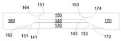
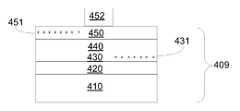
여기에서 기재되는 바와 같은 스위칭 디바이스의 실시예는 도 1a에 도시될 수 있다. 예시적인 스위칭 디바이스는 제 1 반도체층(130), 절연층(140), 제 2 반도체층(150), 제 1 금속 접촉부(160) 및 제 2 금속 접촉부(170)를 포함한다. 도 1a에 도시되는 바와 같이, 절연층(140)(실시예들에서, 제 1 절연층(140)으로 또한 지칭될 수 있음)은 제 1 반도체층(130)과 제 2 반도체층(150) 사이에 위치될 수 있다. 실시예들에서, 절연층(140)은 제 1 반도체층(130) 및 제 2 반도체층(150) 사이에 직접 위치될 수 있으며, 제 1 반도체층(130)과 제 2 반도체층(150) 모두와 접촉한다.An embodiment of a switching device as described herein can be shown in Figure 1A. The exemplary switching device includes a
실시예들에서, 제 1 금속 접촉부(160)는 제 1 반도체층(130), 절연층(140) 및 제 2 반도체층(150)에 인접한다. 실시예들에서, 제 1 금속 접촉부(160)는 제 1 반도체층(130), 절연층(140) 및 제 2 반도체층(150)의 제 1 부분들(131, 141 및 151) 각각에 인접한다. 실시예들에서, 제 1 금속 접촉부(160)는 제 1 반도체층(130), 절연층(140) 및 제 2 반도체층(150)의 제 1 부분들(131, 141 및 151)과 접촉한다. 실시예들에서, 제 1 금속 접촉부(160)는 제 1 반도체층(130), 절연층(140) 및 제 2 반도체층(150)의 제 1 부분들(131, 141 및 151)과 직접 접촉한다.In embodiments, the
실시예들에서, 제 2 금속 접촉부(170)는 제 1 반도체층(130), 절연층(140) 및 제 2 반도체층(150)에 인접한다. 실시예들에서, 제 2 금속 접촉부(170)는 제 1 반도체층(130), 절연층(140) 및 제 2 반도체층(150)의 제 2 부분들(133, 143 및 153) 각각에 인접한다. 실시예들에서, 제 2 금속 접촉부(170)는 제 1 반도체층(130), 절연층(140) 및 제 2 반도체층(150)의 제 2 부분들(133, 143 및 153)과 접촉한다. 실시예들에서, 제 2 금속 접촉부(170)는 제 1 반도체층(130), 절연층(140) 및 제 2 반도체층(150)의 제 2 부분들(133, 143 및 153)과 직접 접촉한다.In embodiments, the
제 1 반도체층(130)의 제 1 부분(131)은 제 1 접합부(162)에서 제 1 금속 접촉부(160)와 접촉하고; 제 2 반도체층(150)의 제 1 부분(151)은 제 2 접합부(164)에서 제 1 금속 접촉부(160)와 접촉하고; 제 1 반도체층(130)의 제 2 부분(133)은 제 3 접합부(172)에서 제 2 금속 접촉부(170)와 접촉하고; 제 2 반도체층(150)의 제 2 부분(153)은 제 4 접합부(174)에서 제 2 금속 접촉부(170)와 접촉한다. 제 1, 제 2, 제 3 및 제 4 접합부들(162, 164, 172 및 174)은 오믹(ohmic) 또는 쇼트키 접합부들이다.The
금속 및 반도체가 밀접하게 접촉할 때마다, 대부분의 전하 캐리어들(전자(electron)들 또는 홀(hole)들)이 하나의 재료로부터 다른 재료로 통과하는 것을 방해하는 두 재료들 사이의 전위 장벽이 존재한다. 오직 소수의 캐리어들만이 장벽을 극복하기에 충분한 에너지를 가지며, 다른 재료로 건너간다. 바이어스가 접합부에 인가될 때, 바이어스는 두 효과들 중 하나를 가질 수 있다: 바이어스는 장벽이 반도체 측으로부터 낮게 나타나게 할 수 있거나, 또는 바이어스는 장벽이 반도체 측으로부터 높게 나타나게 할 수 있다. 바이어스는 금속 측으로부터의 장벽 높이를 변경하지 않는다. 이것의 결과는 쇼트키 접합 또는 정류성 접촉(rectifying contact)으로 또한 지칭될 수 있는 쇼트키 장벽이고, 여기서 접합은 하나의 바이어스 극성에 대하여 도통(conduct)되지만, 다른 극성에 대해서는 도통되지 않는다. 반면에, 오믹 접촉들은 두 극성들 모두에 대해서 동일하게 도통된다. 오믹 접촉 또는 오믹 접합은 선형적 그리고 대칭적 전류-전압(I-V) 곡선을 갖고; 쇼트키 접촉 또는 쇼트키 접합은 비선형적 그리고 비대칭적 전류-전압(I-V) 곡선을 갖는다.A potential barrier between two materials that prevents most of the charge carriers (electrons or holes) from passing from one material to another material every time the metal and semiconductor are in intimate contact exist. Only a small number of carriers have enough energy to overcome the barrier and cross over to another material. When a bias is applied to a junction, the bias may have one of two effects: the bias may cause the barrier to appear lower from the semiconductor side, or the bias may cause the barrier to appear higher from the semiconductor side. The bias does not change the barrier height from the metal side. The result of this is a Schottky barrier, which can also be referred to as a Schottky junction or a rectifying contact, where the junction is conducted for one bias polarity, but not for the other polarity. On the other hand, ohmic contacts are equally conductive for both polarities. The ohmic contact or ohmic junction has a linear and symmetrical current-voltage (I-V) curve; Schottky contacts or Schottky junctions have non-linear and asymmetrical current-voltage (I-V) curves.
특정 금속-반도체 접합이 오믹 접합일 것인지 또는 쇼트키 접합일 것인지는 금속의 일 함수(work function), 반도체의 밴드 갭(band gap), 반도체 내의 도펀트들의 타입 및 농도, 및 다른 인자들에 적어도 부분적으로 의존할 수 있다. 일반적으로, 고농도로 도핑된 반도체와 금속의 접합은 더 얇은 에너지 장벽을 형성한다(도펀트 레벨이 고농도일수록, 장벽은 더 얇아질 것임). 역 바이어스 상태들에서, 전하는 양자 역학적 터널링(quantum mechanical tunneling)으로 인하여 장벽을 통해 흐를 것이다. 실시예들에서, 고농도로 도핑된 반도체 재료와 금속의 접합은 오믹 접합을 형성할 것이고(전류는 양쪽 방향으로 흐를 수 있다: 순방향 바이어싱된 전류는 하나의 방향으로, 터널링은 다른(역) 방향으로), 도핑되지 않거나 저농도로 도핑된 반도체 재료와 금속의 접합은 쇼트키 접합을 형성할 것이다.Whether the particular metal-semiconductor junction is an ohmic junction or a Schottky junction is determined at least in part by the work function of the metal, the band gap of the semiconductor, the type and concentration of dopants in the semiconductor, You can depend on it. Generally, the junction of heavily doped semiconductors and metals forms a thinner energy barrier (the higher the dopant level, the thinner the barrier will be). In reverse bias states, the charge will flow through the barrier due to quantum mechanical tunneling. In embodiments, the junction of the heavily doped semiconductor material and the metal will form an ohmic junction (the current can flow in both directions: forward biased current in one direction, tunneling in the other (reverse) direction ), The junction of the undoped or lightly doped semiconductor material with the metal will form a Schottky junction.
여기에서 기재되는 스위칭 엘리먼트들의 실시예들에서, 제 1 반도체층(130)은 하나의 오믹 접촉 및 하나의 쇼트키 접촉을 가질 것이고, 제 2 반도체층(150)은 하나의 오믹 접촉 및 하나의 쇼트키 접촉을 가질 것이다. 제 1 반도체층(130) 내의 쇼트키 접촉 및 오믹 접촉의 배향은 일반적으로 제 2 반도체층(150) 내의 쇼트키 접촉 및 오믹 접촉의 배향의 반대일 것이다. 실시예들에서, 제 1 접합부(162)는 쇼트키 접합부일 수 있고, 제 2 접합부(164)는 오믹 접합부일 수 있으며, 제 3 접합부(172)는 오믹 접합부일 수 있고, 제 4 접합부(174)는 쇼트키 접합부일 수 있다. 실시예들에서, 제 1 접합부(162)는 오믹 접합부일 수 있고, 제 2 접합부(164)는 쇼트키 접합부일 수 있으며, 제 3 접합부(172)는 쇼트키 접합부일 수 있고, 제 4 접합부(174)는 오믹 접합부일 수 있다.In embodiments of the switching elements described herein, the
제 1 및 제 2 반도체층들(130 및 150) 내의 쇼트키 접촉들과 오믹 접촉들의 반대 배향은 양방향 스위치의 이러한 구성을 갖는 스위칭 엘리먼트들을 형성한다. 양방향 스위치는 제 1 극성을 갖는 전류가 인가되는 경우 제 1 방향으로 전류가 흐르게 하고, 제 2 극성(제 1 극성의 반대)을 갖는 전류가 인가되는 경우 제 2 방향(제 1 방향의 반대)으로 전류가 흐르게 한다. 도 1b는 여기에서 기재되는 스위칭 엘리먼트들의 양방향 특성을 예시하는 회로도를 도시한다. 도 1b의 회로도에 도시되는 바와 같이, 제 1 반도체층 및 제 2 반도체층은 병렬인 제 1 다이오드(180) 및 제 2 다이오드(185)의 기능을 각각 제공한다. 제 1 다이오드(180)는 제 2 다이오드(185)에서 전류가 흐르는 반대 방향으로 전류가 흐르게 한다. 도 1c는 기재되는 가설적인 스위칭 엘리먼트에 대한 전류-전압(I-V) 곡선을 도시한다. 도 1c에 도시되는 바와 같이, 제 1 다이오드(180)는 실질적인 전류가 제 1 방향으로 흐르기 시작하는 임계 전압(VT1)을 갖고; 제 2 다이오드(185)는 실질적인 전류가 제 2 방향으로 흐르기 시작하는 임계 전압(VT2)을 갖는다. 도 1c에 도시되는 바와 같이, 두 전압들에서 스위칭 엘리먼트로부터 흐르는 전류와 같이, VT1 및 VT2의 극성은 반대이다. 이것은, 전압 VT1과 전압 VT2 사이의 전류를 본질적으로 차단하며, 제 1 극성을 갖는 전류가 VT2 미만의 전압들에서 흐르게 하고, 제 2 극성을 갖는 전류가 VT1 초과의 전압들에서 흐르게 하는 스위칭 엘리먼트를 제공한다.The opposite orientation of Schottky contacts and ohmic contacts in the first and second semiconductor layers 130 and 150 forms the switching elements with this configuration of bi-directional switches. The bidirectional switch causes a current to flow in a first direction when a current having a first polarity is applied and a second direction (opposite to the first direction) when a current having a second polarity Current flows. Figure IB shows a circuit diagram illustrating the bi-directional characteristics of the switching elements described herein. As shown in the circuit diagram of FIG. 1B, the first semiconductor layer and the second semiconductor layer provide the functions of a
스위치로서의 기능에서, 이것은, VT2보다 적은 전압이 스위칭 엘리먼트에 인가되는 경우 전류가 제 1 방향으로 흐를 것인 반면, VT1보다 큰 전압이 스위칭 엘리먼트에 인가되는 경우 전류가 제 2 방향으로 흐를 것임을 의미한다. 따라서, 스위칭 엘리먼트는 예를 들어, 비휘발성 메모리 셀과 같은 전기적으로 접속되는 컴포넌트를 통해 전류가 흐르는 방향을 제어하는 데에 이용될 수 있다.In functioning as a switch this means that the current will flow in the first direction when a voltage less than VT2 is applied to the switching element while the current will flow in the second direction if a voltage greater than VT1 is applied to the switching element it means. Thus, the switching element can be used to control the direction of current flow through an electrically connected component, such as, for example, a non-volatile memory cell.
여기에서 기재되는 바와 같은 스위칭 엘리먼트들은 양방향 스위칭 및 높은 구동 전류를 견디는 능력의 결합을 유리하게 제공할 수 있다. 상대적으로 많은 양의 전류가 흐를 수 있게 하는 기재되는 스위칭 엘리먼트의 전류 경로의 (종래의 MOS 트랜지스터들에 비해) 상대적으로 더 큰 단면으로 인하여 높은 구동 전류가 필요한 경우, 여기에서 기재되는 스위칭 엘리먼트들이 사용될 수 있다. (스핀 토크 전달 랜덤 액세스 메모리(STRAM)의 예와 같이) 높은 구동 전류가 필요한 경우 또는 요구되는 경우, 스위치가 컴포넌트들과 함께 이용될 수 있기 때문에, 높은 구동 전류들을 처리하는 능력은 유리할 수 있다.The switching elements as described herein can advantageously provide a combination of bi-directional switching and the ability to withstand high drive currents. If a higher drive current is required due to the relatively larger cross-section (compared to conventional MOS transistors) of the current path of the described switching element, which allows a relatively large amount of current to flow, . The ability to handle high drive currents may be advantageous, as a switch may be used with components, if or when a high drive current is needed (such as in an example of a spin torque transfer random access memory (STRAM)).
도 2a는 여기에서 기재되는 스위칭 엘리먼트의 또 다른 실시예를 도시한다. 도 2a에서의 스위칭 엘리먼트는 상기 논의되는 컴포넌트들을 포함하며, 또한 다른 컴포넌트들을 포함한다. 예를 들어, 제 2 절연층(220)으로 또한 지칭될 수 있는 또 다른 절연층(220)이 제 1 반도체층(230)에 인접할 수 있다. 실시예들에서, 제 2 절연층(220)은 제 1 반도체층(230)에 바로 인접할 수 있다. 제 2 절연층(220)은 제 1 반도체층(230)을 기판(210)으로부터 전기적으로 절연하기 위한 기능을 할 수 있다. 기판은 전기적으로 전도성이 있거나, 반도체 재료일 수 있다. 기판(210)은 스위칭 엘리먼트 구조적 안정성을 제공하기 위한 기능을 할 수 있으며, 스위칭 엘리먼트의 형성 프로세스를 보조할 수 있다.Figure 2a shows another embodiment of the switching element described herein. The switching element in FIG. 2A includes the components discussed above and also includes other components. For example, another insulating
도 1c에 도시되는 가설적인 I-V 곡선은 대칭적이다. 일반적으로, 기재되는 스위칭 엘리먼트의 I-V 곡선이 대칭적이게 하기 위해서, 제 1 반도체층 및 제 2 반도체층에 걸친 경로 길이들은 적어도 실질적으로 동일하여야 하고, 금속/반도체 접합부들(예를 들어, 162, 164, 172 및 174)의 표면 영역은 적어도 실질적으로 동일하여야 한다. 대칭적 제 1 및 제 2 반도체층들을 갖지 않는 스위칭 엘리먼트 및/또는 실질적으로 동일한 표면 영역들은 덜 비대칭적이 되도록 변경될 수 있다. 이것은 예를 들어, 스위칭 엘리먼트를 구성하는 컴포넌트들을 변경함으로써, 도펀트들(아이덴티티(identity) 또는 양)을 변경함으로써, 금속 접촉부들 중 하나 또는 모두를 변경함으로써, 여기에서 논의되지 않은 다른 인자들을 변경함으로써, 또는 이들 인자들의 결합을 변경함으로써 이루어질 수 있다. 대칭적 I-V 곡선을 갖는 스위칭 엘리먼트는 일부 애플리케이션들에서 유리할 수 있다. 예를 들어, 메모리 엘리먼트들과 결합하여 사용될 스위칭 엘리먼트가 대칭적 I-V 곡선을 갖는 것이 유리할 수 있다.The hypothetical I-V curve shown in Fig. 1C is symmetrical. Generally, the path lengths across the first and second semiconductor layers must be at least substantially the same, and the metal / semiconductor junctions (e.g., 162, 164, 172, and 174) should be at least substantially the same. The switching elements without symmetrical first and second semiconductor layers and / or substantially the same surface areas can be modified to be less asymmetric. This can be accomplished by changing one or both of the metal contacts, for example, by changing the components making up the switching element, by changing the dopants (identity or amount), by changing other factors not discussed herein , Or by changing the combination of these factors. Switching elements with symmetrical I-V curves may be advantageous in some applications. For example, it may be advantageous for a switching element to be used in combination with memory elements to have a symmetrical I-V curve.
제 1 및 제 2 반도체층들의 두께를 실질적으로 동일하게 만드는 것은 상대적으로 간단한 일이기 때문에, 도 2a에 도시되는 예시적인 스위칭 엘리먼트는 대칭적인 I-V 곡선을 갖도록 상대적으로 용이하게 제조될 수 있다. 실시예들에서, 실질적으로 동일한 두께를 갖는 제 1 반도체층 및 제 2 반도체층을 갖는 스위칭 엘리먼트는 대칭적 I-V 곡선을 가질 수 있을 것이다.Since making the thicknesses of the first and second semiconductor layers substantially the same is relatively simple, the exemplary switching element shown in Fig. 2A can be manufactured relatively easily to have a symmetrical I-V curve. In embodiments, a switching element having a first semiconductor layer and a second semiconductor layer having substantially the same thickness may have a symmetrical I-V curve.
도 2b에 도시되는 예시적인 스위칭 엘리먼트는 대칭적 I-V 곡선을 갖지 않을 수 있을 것이다. 도 2b에 도시되는 바와 같이, 도시되는 스위칭 엘리먼트는 제 2 반도체층(250)보다 상당히 두꺼운 제 1 반도체층(230)을 가지며; 제 1 반도체층(230)의 접합부들인 제 1 접합부(262) 및 제 3 접합부(274)는 제 2 반도체층(250)의 접합부들(즉, 제 1 금속 접촉부(260) 및 제 2 금속 접촉부(270)와의 제 2 접합부(264) 및 제 4 접합부(272))보다 상당히 많은 표면 영역을 갖는다. 이것은 제 1 반도체층(230)이 제 2 반도체층(250)보다 더 높은 임계 전압을 갖게 할 수 있을 것이다. 따라서, 이러한 스위칭 엘리먼트는 비대칭적 I-V 곡선을 가질 수 있을 것이다.The exemplary switching element shown in Figure 2B may not have a symmetric I-V curve. As shown in FIG. 2B, the switching element shown has a
제 1 반도체층 및 제 2 반도체층은 임의의 반도체 재료를 포함할 수 있다. 제 1 반도체층 및 제 2 반도체층은 동일한 재료일 수 있지만, 동일한 재료일 필요는 없다. 제 1 반도체층, 제 2 반도체층 또는 이 둘 모두에 이용될 수 있는 예시적인 반도체들은 실리콘, 실리콘 함유 화합물들, 게르마늄, 게르마늄 함유 화합물들, 알루미늄 함유 화합물들, 붕소 함유 화합물들, 갈륨 함유 화합물들, 인듐 함유 화합물들, 카드뮴 함유 화합물들, 아연 함유 화합물들, 납 함유 화합물들, 주석 함유 화합물들을 포함하지만, 이들로 제한되지 않는다. 예시적인 원소 반도체 및 화합물 반도체는 실리콘 예를 들어, 결정질 실리콘, 게르마늄, 실리콘 탄화물(SiC), 실리콘 게르마늄(SiGe), 알루미늄 안티몬화물(AlSb), 알루미늄 비화물(AlAs), 알루미늄 질화물(AlN), 알루미늄 인화물(AlP), 붕소 질화물(BN), 붕소 인화물(BP), 붕소 비화물(BAs), 갈륨 안티몬화물(GaSb), 갈륨 비화물(GaAs), 갈륨 질화물(GaN), 갈륨 인화물(GaP), 인듐 안티몬화물(InSb), 인듐 비화물(InAs), 인듐 질화물(InN), 인듐 인화물(InP), 알루미늄 갈륨 비화물(AlGaAs, AlxGa1-xAs), 인듐 갈륨 비화물(InGaAs, InxGal-xAs), 인듐 갈륨 인화물(InGaP), 알루미늄 인듐 비화물(AlInAs), 알루미늄 인듐 안티몬화물(AlInAs), 갈륨 비화물 질화물(GaAsN), 갈륨 비화물 인화물(GaAsP), 알루미늄 갈륨 질화물(AlGaN), 알루미늄 갈륨 인화물(AlGaP), 인듐 갈륨 질화물(InGaN), 인듐 비화물 안티몬화물(InAsSb), 인듐 갈륨 안티몬화물(InGaSb), 알루미늄 갈륨 인듐 인화물(AlGaInP, 또한 InAlGaP, InGaAlP, AlInGaP), 알루미늄 갈륨 비화물 인화물(AlGaAsP), 인듐 갈륨 비화물 인화물(InGaAsP), 알루미늄 인듐 비화물 인화물(AlInAsP), 알루미늄 갈륨 비화물 질화물(AlGaAsN), 인듐 갈륨 비화물 질화물(InGaAsN), 인듐 알루미늄 비화물 질화물(InAlAsN), 갈륨 비화물 안티몬화물 질화물(GaAsSbN), 갈륨 인듐 질화물 비화물 안티몬화물(GaInNAsSb), 갈륨 인듐 비화물 안티몬화물 인화물(GaInAsSbP), 카드뮴 셀렌화물(CdSe), 카드뮴 황화물(CdS), 카드뮴 텔루르화물(CdTe), 아연 산화물(ZnO), 아연 셀렌화물(ZnSe), 아연 황화물(ZnS), 아연 텔루르화물(ZnTe), 카드뮴 아연 텔루르화물(CdZnTe, CZT), 수은 카드뮴 텔루르화물(HgCdTe), 수은 아연 텔루르화물(HgZnTe), 수은 아연 셀렌화물(HgZnSe), 제일구리 염화물(CuCl), 납 셀렌화물(PbSe), 납 황화물(PbS), 납 텔루르화물(PbTe), 주석 황화물(SnS), 주석 텔루르화물(SnTe), 납 주석 텔루르화물(PbSnTe), 탈륨 주석 텔루르화물(T12SnTe5), 탈륨 게르마늄 텔루르화물(Tl2GeTe5), 비스무트 텔루르화물(Bi2Te3), 카드뮴 인화물(Cd3P2), 카드뮴 비화물(Cd3As2), 카드뮴 안티몬화물(Cd3Sb2), 아연 인화물(Zn3P2), 아연 비화물(Zn3As2) 및 아연 안티몬화물(Zn3Sb2)을 포함하지만, 이들로 제한되지 않는다.The first semiconductor layer and the second semiconductor layer may comprise any semiconductor material. The first semiconductor layer and the second semiconductor layer may be the same material, but they need not be the same material. Exemplary semiconductors that may be used for the first semiconductor layer, the second semiconductor layer, or both include silicon, silicon containing compounds, germanium, germanium containing compounds, aluminum containing compounds, boron containing compounds, gallium containing compounds , Indium containing compounds, cadmium containing compounds, zinc containing compounds, lead containing compounds, tin containing compounds. Exemplary elemental semiconductors and compound semiconductors include silicon, for example, crystalline silicon, germanium, silicon carbide (SiC), silicon germanium (SiGe), aluminum antimonides (AlSb), aluminum halides (AlAs) (AlP), boron nitride (BN), boron phosphide (BP), boron paraffin (BAs), gallium antimonide (GaSb), gallium arsenide (GaAs), gallium nitride (GaN), gallium phosphide (InGaAs, InxGal-xAs), indium antimonides (InSb), indium arsenide (InAs), indium nitride (InN), indium phosphide (InP), aluminum gallium arsenide (AlGaAs, AlxGa1- , Gallium arsenide phosphide (InGaP), aluminum indium arsenide (AlInAs), aluminum indium antimonide (AlInAs), gallium arsenide nitride (GaAsN), gallium arsenide phosphide (GaAsP), aluminum gallium nitride (AlGaN) (AlGaP), indium gallium nitride (InGaN), indium parate antimonide (InAsSb), phosphorus Aluminum gallium indium phosphide (AlGaInP, also InAlGaP, InGaAlP, AlInGaP), aluminum gallium arsenide non-oxide phosphide (AlGaAsP), indium gallium arsenide oxide phosphide (InGaAsP), aluminum indium arsenide phosphide (AlInAsP), aluminum (GaAs), gallium indium nitride (GaInNAsSb), indium gallium indium nitride (InAlAsN), gallium arsenide nitride (GaAsSbN), indium gallium arsenide nitride (InGaAsN) Cadmium sulfide (CdSe), cadmium telluride (CdTe), zinc oxide (ZnO), zinc selenide (ZnSe), zinc sulfide (ZnS), zinc telluride (ZnTe), cadmium zinc telluride (CdZnTe, CZT), mercury cadmium telluride (HgCdTe), mercury zinc telluride (HgZnTe), mercury zinc selenide (HgZnSe), cuprous chloride ), Lead sulfur Water (PbS), lead telluride cargo (PbTe), tin sulfide (SnS), tin telluride cargo (SnTe), lead tin telluride cargo (PbSnTe), thallium tin telluride cargo (T12 SnTe5), thallium, germanium tellurium cargo (Tl2 GeTe5), bismuth telluride cargo (Bi2 Te3), cadmium phosphide (Cd3 P2), cadmium arsenide (Cd3 As2), cadmium antimonide (Cd3 Sb2), zinc phosphide (Zn3 P2 ), zinc paraffin (Zn3 As2 ), and zinc antimonide (Zn3 Sb2 ).
제 1 반도체층 및 제 2 반도체층 모두의 일부는 도핑된다. 도핑은 반도체의 전기적 속성들을 변경하기 위해서 불순물들을 반도체로 의도적으로 첨가(introduce)하는 프로세스이다. 선택된 특정 도펀트는 최종 스위칭 엘리먼트에서 요구되는 특정 속성들, 도핑될 반도체 재료의 아이덴티티, 여기에서 논의되지 않은 다른 인자들 또는 이들의 결합에 적어도 부분적으로 의존할 수 있다. 예시적인 도펀트들은 Ⅲ족 및 Ⅴ족 원소들을 포함할 수 있지만, 이들로 제한되지 않는다. 반도체 재료들이 Ⅳ족 재료들(예를 들어, 실리콘, 게르마늄 및 실리콘 탄화물)인 경우, Ⅲ족 또는 Ⅴ족 원소들이 도펀트들로서 이용될 수 있다. 구체적인 예시적 도펀트들은 붕소(B), 비화물(As), 인화물(P) 및 갈륨(Ga)을 포함할 수 있지만, 이들로 제한되지 않는다.A portion of both the first semiconductor layer and the second semiconductor layer is doped. Doping is the process of intentionally introducing impurities into a semiconductor to change the electrical properties of the semiconductor. The particular dopant selected may depend at least in part on the specific attributes required in the final switching element, the identity of the semiconductor material to be doped, other factors not discussed herein, or a combination thereof. Exemplary dopants may include, but are not limited to, Group III and Group V elements. If the semiconductor materials are Group IV materials (e.g., silicon, germanium and silicon carbide), Group III or Group V elements may be used as dopants. Specific exemplary dopants may include, but are not limited to, boron (B), arsenide (As), phosphide (P) and gallium (Ga).
제 1 절연층 및 선택적 제 2 절연층은 전기적으로 절연성인 임의의 재료로 이루어질 수 있다. 제 1 절연층 및 선택적 제 2 절연층은 동일한 재료일 수 있지만, 동일한 재료일 필요는 없다. 예시적인 절연 재료들은 예를 들어, 알루미나(Al2O3), 실리콘 산화물(SiO2) 및 마그네슘 산화물(MgO)과 같은 산화물을 포함하지만, 이에 제한되지 않는다.The first insulating layer and the optional second insulating layer may be made of any material that is electrically insulating. The first insulating layer and the selective second insulating layer may be the same material, but they need not be the same material. Exemplary insulation materials include, for example, include an oxide such as alumina (Al2 O3), silicon oxide (SiO2) and magnesium oxide (MgO), but is not limited to this.
금속 접촉부들은 전기적으로 전도성이 있는 임의의 금속 재료로 이루어질 수 있다. 제 1 금속 접촉부 및 제 2 금속 접촉부는 동일한 재료일 수 있지만, 동일한 재료일 필요는 없다. 예시적인 전기적 전도성 금속 재료들은 텅스텐(W) 또는 귀금속 예를 들어, 금(Au), 플래티늄(Pt), 팔라듐(Pd), 로듐(Rh), 구리(Cu), 니켈(Ni), 은(Ag), 코발트(Co), 철(Fe) 또는 이들의 규화물들을 포함하지만, 이들로 제한되지 않는다.The metal contacts may be made of any electrically conductive metal material. The first metal contact and the second metal contact may be the same material, but need not be of the same material. Exemplary electrically conductive metal materials include tungsten (W) or noble metals such as gold (Au), platinum (Pt), palladium (Pd), rhodium (Rh), copper (Cu), nickel (Ni) ), Cobalt (Co), iron (Fe), or silicides thereof.
실시예들에서, 제 1 및 제 2 반도체층들 모두는 결정질 실리콘으로 이루어진다. 실시예들에서, 제 1 및 제 2 반도체층들은 붕소, 인화물 또는 비화물로 도핑된다. 실시예들에서, 제 1 절연층 및 제 2 절연층은 존재하는 경우, 실리콘 산화물(SiO2)로 이루어진다. 실시예들에서, 금속 접촉부들은 텅스텐(W), 니켈 규화물 또는 코발트 규화물이다.In embodiments, both the first and second semiconductor layers are made of crystalline silicon. In embodiments, the first and second semiconductor layers are doped with boron, phosphide, or incombination. In embodiments, it comprises a first insulating layer and second insulating layer, if present, silicon oxide (SiO2). In embodiments, the metal contacts are tungsten (W), nickel silicide, or cobalt silicide.
도 2a에 도시되는 바와 같은 스위칭 엘리먼트에 대한 제조의 예시적인 방법은 도 3에 제공되며, 도 4a 내지 4g에서 단계적으로 설명된다. 일반적으로, 이러한 제조 방식들은 포토리소그래피(photolithography) 기법들 및 다른 제거 기법들 예를 들어, 에칭, 및 화학 기계적 연마(CMP)를 포함하는 반도체 제조 방법들을 포함할 수 있다. 플라즈마 기상 증착(PVD), 이온화 플라즈마 기반 스퍼터링(sputtering), 롱 쓰로우(long throw) 스퍼터링, 화학 기상 증착(CVD), 원자층 증착(ALD) 및 유기 금속 화학 기상 증착(MOCVD)을 포함하지만 이들로 제한되지 않는 증착 방법들은 예시적인 방법으로 증착되는 다양한 층들을 증착시키는 데에 이용될 수 있다. 도 3에 도시되는 단계들 및 도 4a 내지 4g에서의 이들의 도면은 본 명세서에 기재되는 바와 같은 스위칭 엘리먼트가 제조될 수 있는 방식을 결코 제한하지 않는다. 또한, 도 4a 내지 4g는 반드시 실제 크기 비율이지 않으며, 반드시 준비의 매 상태에서의 물품(article)을 도시하는 것은 아니고, 즉, 물품의 일부 중간 단계들이 도면들의 시퀀스에 도시되지 않을 수 있다는 점에 유의하여야 한다. 또한, 도 4a 내지 4g에 대하여 논의된 재료들 및 프로세스들은 본 명세서에 이용될 수 있는 재료들 또는 프로세스들을 결코 제한하지 않는다.An exemplary method of fabrication for a switching element as shown in Fig. 2A is provided in Fig. 3 and is described stepwise in Figs. 4A-4G. In general, these fabrication methods may include semiconductor manufacturing methods including photolithography techniques and other removal techniques such as etching, and chemical mechanical polishing (CMP). Including but not limited to plasma enhanced chemical vapor deposition (PVD), ionized plasma based sputtering, long throw sputtering, chemical vapor deposition (CVD), atomic layer deposition (ALD) and metalorganic chemical vapor deposition May be used to deposit the various layers deposited in an exemplary manner. The steps shown in Fig. 3 and their views in Figs. 4A-4G never limit the manner in which the switching elements can be manufactured as described herein. It should also be noted that Figures 4A-4G are not necessarily to scale and do not necessarily illustrate an article in every state of preparation, that is, some intermediate steps of the article may not be shown in the sequence of figures Be careful. In addition, the materials and processes discussed with respect to Figures 4A-4G never limit the materials or processes that may be used herein.
도 3 및 도 4a 내지 4g에 도시되는 예시적인 방법은 기판의 사용을 도시한다. 당업자는 본 명세서를 판독함으로써, 기판의 사용이 필수적이지 않고, 여기에서 기재되는 바와 같은 스위칭 엘리먼트들이 기판의 사용 없이 제조될 수 있으며, 스위칭 엘리먼트가 제조 이후 지지물 상에 배치될 수 있고, 기판이 이용되고 이후 스위칭 엘리먼트의 제조 동안 또는 이후에 제거될 수 있으며, 또는 기판은 전혀 이용될 필요가 없다는 것을 이해할 것이다. 기판은 이용되는 경우, 실리콘, 실리콘 및 게르마늄의 혼합물, 또는 다른 유사한 재료들과 같은 재료들을 포함할 수 있다.The exemplary method illustrated in Figures 3 and 4A-4G illustrates the use of a substrate. Those skilled in the art will recognize that the use of a substrate is not essential, the switching elements as described herein can be fabricated without the use of a substrate, the switching element can be placed on a support after fabrication, And then removed during or after the fabrication of the switching element, or the substrate need not be used at all. The substrate, when utilized, may include materials such as silicon, a mixture of silicon and germanium, or other similar materials.
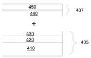
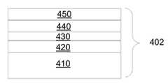
여기에서 기재되는 스위칭 엘리먼트를 제조하는 예시적인 방법을 도시하는 흐름도가 도 3에 도시된다. 예시적인 방법에서의 제 1 단계는 적층 물품(layered article)을 제공하는 단계(310)이다. 적층 물품은 적어도 제 1 반도체층, 절연층(제 1 절연층으로 또한 지칭될 수 있음) 및 제 2 반도체층을 포함하며, 제 1 반도체층과 제 2 반도체층 사이에 위치되는 절연층을 갖는다. 예시적인 적층 물품(402)은 도 4b에 도시될 수 있으며, 기판(410), 제 2 절연층(420), 제 1 반도체층(430), 제 1 절연층(440) 및 제 2 반도체층(450)을 포함한다. 본 명세서를 판독함으로써, 적층 물품이 도 4b에 도시되는 층들보다 더 많거나 더 적은 층들을 가질 수 있다는 것이 이해되어야 한다. 적층 물품은 예를 들어, 상업적으로 이용가능한 소스들을 통해 제조 또는 획득될 수 있다.A flow chart illustrating an exemplary method of fabricating the switching elements described herein is shown in FIG. The first step in the exemplary method is step 310 of providing a layered article. The laminated article has at least a first semiconductor layer, an insulating layer (which may also be referred to as a first insulating layer) and a second semiconductor layer, and an insulating layer positioned between the first semiconductor layer and the second semiconductor layer. An exemplary
적층 물품을 제조하는 데에 이용될 수 있는 예시적인 선택적 단계들은 단계들(302, 304 및 306)에 도시된다. 단계(302)는 제 1 적층 구조를 제공하는 단계를 포함한다. 제 1 적층 구조는 적어도 제 1 기판, 제 2 절연층 및 제 1 반도체층을 포함할 수 있으며, 제 1 기판과 제 1 반도체층 사이에 위치되는 제 2 절연층을 갖는다. 제 1 적층 구조의 예는 기판 상에 배치되는 절연층 및 절연층 상에 배치되는 제 1 반도체층을 갖는 기판(예를 들어, 실리콘 웨이퍼)을 포함할 수 있다. 제 1 적층 구조의 절연층(제 2 절연층)은 기판(예를 들어, SiO2)의 일부로부터 절연 재료를 형성하기 위해서, 절연 재료를 증착시킴으로써 또는 기판의 일부를 산화시킴으로써 형성될 수 있다. 예시적인 제 1 적층 구조(405)가 도 4a에 도시되며, 기판(410), 제 2 절연층(420) 및 제 1 반도체층(430)을 포함한다.Exemplary optional steps that may be used to produce the laminated article are shown in
단계(304)는 제 2 적층 구조를 제공하는 단계를 포함한다. 제 2 적층 구조는 적어도 절연층(제 1 절연층으로 지칭될 수 있음) 및 제 2 반도체층을 포함할 수 있으며, 제 2 반도체층 상에 배치되는 절연층(또는 절연층 상에 배치되는 제 2 반도체층)을 갖는다. 제 2 적층 구조의 예는 산화된 기판(예를 들어, 실리콘 웨이퍼)을 포함할 수 있으며, 여기서 산화된 부분은 절연층이 되며, 산화되지 않은 부분은 제 2 반도체층이 된다. 대안적으로, 반도체 재료(예를 들어, 실리콘 웨이퍼)는 제 2 반도체층 상에 절연층을 형성하기 위해서 반도체 재료 상에 배치되는 절연 재료를 가질 수 있다. 실시예들에서, 실리콘 웨이퍼와 같은 기판이 제 2 적층 구조를 형성하는 데에 이용되는 경우, 실리콘 웨이퍼의 일부는 제 2 반도체층의 두께를 조절하기 위해서 제거될 수 있다. 이것은 예를 들어, 화학 기계적 평탄화(planning)(CMP)와 같은 기법들을 사용하여 이루어질 수 있다. 예시적인 제 2 적층 구조(407)는 도 4a에 도시되며, 절연층(440) 및 제 2 반도체층(450)을 포함한다.Step 304 includes providing a second laminate structure. The second stacked structure may include at least an insulating layer (which may be referred to as a first insulating layer) and a second semiconductor layer, and an insulating layer disposed on the second semiconductor layer (or a second Semiconductor layer). An example of a second stacked structure may include an oxidized substrate (e.g., a silicon wafer), wherein the oxidized portion is an insulating layer and the unoxidized portion is a second semiconductor layer. Alternatively, a semiconductor material (e.g., a silicon wafer) may have an insulating material disposed on the semiconductor material to form an insulating layer on the second semiconductor layer. In embodiments, when a substrate, such as a silicon wafer, is used to form the second laminate structure, a portion of the silicon wafer may be removed to adjust the thickness of the second semiconductor layer. This can be done, for example, using techniques such as chemical mechanical planarization (CMP). An exemplary
단계(306)는 제 2 적층 구조와 접촉하는 제 1 적층 구조를 배치(또는 제 1 적층 구조와 접촉하는 제 2 적층 구조를 배치)하는 단계를 포함한다. 적층 물품을 형성하기 위해서 제 2 적층 구조의 절연층이 제 1 적층 구조의 제 1 반도체층에 인접하도록 제 1 및 제 2 적층 구조들이 구성된다. 실시예들에서, 제 1 적층 구조의 제 1 반도체 계층은 제 2 적층 구조의 절연층에 바로 인접하거나 이와 직접 접촉한다. 이후, 제 1 및 제 2 적층 구조들은 웨이퍼 본딩 기법들을 사용하여 함께 본딩(bond)될 수 있다. 이 단계의 완료는 도 4b에 도시되는 적층 물품(402)을 형성한다.Step 306 includes placing a first laminate structure in contact with the second laminate structure (or placing a second laminate structure in contact with the first laminate structure). The first and second laminated structures are configured so that the insulating layer of the second laminated structure is adjacent to the first semiconductor layer of the first laminated structure to form the laminated article. In embodiments, the first semiconductor layer of the first stack structure directly contacts or directly contacts the insulating layer of the second stack structure. The first and second stack structures may then be bonded together using wafer bonding techniques. The completion of this step forms the
그러나, (단계들(302, 304 및 306)을 통해서든 또는 다른 방법을 통해서든) 적층 물품이 제공되고, 스위칭 엘리먼트를 형성하는 방법에서의 다음 단계는 적층 물품을 도핑하는 단계(320)이다. 적층 물품을 도핑하는 단계는 제 1 반도체층의 일부 및 제 2 반도체층의 일부를 도핑하기 위한 기능을 할 수 있다. 보다 구체적으로, 적층 물품을 도핑하는 단계는 제 2 반도체층의 제 1 부분 및 제 1 반도체층의 제 2 부분(또는 그 반대도 마찬가지임)을 도핑하기 위한 기능을 한다. 적층 물품을 도핑하기 위해서 착수(undertake)될 수 있는 예시적인 선택적 단계들은 단계들(322, 324, 326 및 328)로 도시된다.However, the stacked article is provided (either through
단계(322)는 제 1 마스크 영역을 형성하는 단계를 포함한다. 마스크 영역들(아래에서 논의될 것인 제 1 마스크 영역 및 제 2 마스크 영역 모두)은 마스크 영역들 아래에 위치되는 재료들로의 도펀트들의 주입을 방지하는 재료들로 이루어진다(문맥 내의 위 및 아래는 도펀트 소스의 위치에 의해 정의되며, 도펀트 소스는 적층 물품의 층들 및 마스크 영역들 모두의 위에 위치됨). 마스크 영역들로서 이용될 수 있는 예시적인 재료들은 산화 재료들, 실리콘 질화물들 또는 포토레지스트를 포함하지만, 이들로 제한되지 않는다. 제 1 마스크 영역은 적층 물품의 일부만을 주입으로부터 보호한다. 도 4c에 도시되는 물품은 제 1 마스크 영역(411)을 포함한다.Step 322 includes forming a first mask region. The mask regions (both the first and second mask regions to be discussed below) are made of materials that prevent the implantation of dopants into the materials located under the mask regions The dopant source being located above both the layers of the stacked article and the mask regions). Exemplary materials that may be used as mask regions include, but are not limited to, oxidized materials, silicon nitrides, or photoresists. The first mask area protects only a portion of the laminated article from injection. The article shown in FIG. 4C includes a
다음 단계(단계(324))는 적층 물품의 일부를 도핑하는 단계를 포함한다. (단계(322)에서 형성되는) 제 1 마스크 영역은 적층 물품의 일부 예를 들어, 제 1 부분의 도핑만을 허용한다. 도 4c에 도시되는 바와 같이, 제 1 마스크 영역 아래로의 주입(화살표에 의해 도시됨)은 방지되며, 제 1 마스크 영역이 적층 물품을 커버하지 않고 있는 부분에는 허용된다. 적층 물품의 제 1 부분의 도핑은 제 1 에너지 레벨을 사용하여 이루어진다. 실시예들에서, 제 1 부분의 도핑은 제 2 반도체층(450)이 고농도로 도핑되게 하고, 제 1 반도체층(430)이 단지 저농도로 도핑되게 하거나 실질적으로 전혀 도핑되지 않게 한다. 차동적인 도핑 레벨들(또는 도핑 및 실질적으로 도핑되지 않음)은 상이한 에너지 레벨들을 사용함으로써 이용될 수 있다.The next step (step 324) includes doping a portion of the laminated article. The first mask region (formed in step 322) allows only a portion of the laminating article, e.g., the doping of the first portion. As shown in FIG. 4C, implantation (shown by the arrows) beneath the first mask area is prevented and allowed in the portion where the first mask area does not cover the laminated article. Doping of the first portion of the laminated article is accomplished using a first energy level. In embodiments, the doping of the first portion causes the
여기에서 도시되는 바와 같이, 단계(324)는 (이 실시예에서 도시되는 바와 같이, 적층 물품의 상부 층인) 제 2 반도체층(450)의 우선적 도핑을 달성한다. 오직 적층 구조의 상부 층 또는 층들의 우선적 도핑은 낮은 주입 에너지를 사용하는 도핑에 의해 이루어질 수 있다. 낮은 에너지를 사용하는 도핑은 특정 깊이를 관통하기에만 충분한 에너지를 도펀트에 제공할 수 있다. 도 4d는 단계(324)의 완료 이후, 제 2 반도체층(450)에 존재하는 도펀트들(451)을 도시한다.As shown here, step 324 achieves preferential doping of the second semiconductor layer 450 (which is the upper layer of the laminated article, as shown in this embodiment). The preferential doping of only the top layer or layers of the laminate structure may be achieved by doping using low implantation energy. Doping using low energy can provide sufficient energy to the dopant to penetrate a certain depth. FIG. 4D shows
단계(326)는 제 2 마스크 영역을 형성하는 단계를 포함한다. 제 2 마스크 영역은 적층 물품의 일부만을 주입으로부터 보호한다. 도 4d에 도시되는 물품은 제 2 마스크 영역(413)을 포함한다. 제 1 마스크 영역(411) 및 제 2 마스크 영역(413)의 위치는 적어도 부분적으로 오버랩될 수 있다. 실시예들에서, 제 1 마스크 영역(411) 및 제 2 마스크 영역(413)은 완전히 오버랩되지 않으며, 단지 부분적으로 오버랩된다. 제 2 마스크 영역(413)은 일반적으로 단계(324)에서 도핑되었던 제 2 반도체층(450)의 적어도 일부를 보호한다. 실시예들에서, 제 2 마스크 영역(413)은 일반적으로 단계(324)에서 도핑되었던 제 2 반도체층(450)의 일부뿐만 아니라 단계(324)에서 도핑되지 않았던 제 2 반도체층(450)의 일부를 보호한다.Step 326 includes forming a second mask region. The second mask region protects only a portion of the laminated article from implantation. The article shown in Fig. 4D includes a
다음 단계(단계(328))는 적층 물품의 일부를 도핑하는 단계를 포함한다. (단계(326)에서 형성되는) 제 2 마스크 영역은 적층 물품의 일부 예를 들어, 제 2 부분의 도핑만을 허용한다. 도 4d에 도시되는 바와 같이, 제 2 마스크 영역 아래로의 주입(화살표에 의해 도시됨)이 방지되며, 제 2 마스크 영역이 적층 물품을 커버하고 있지 않은 부분에는 허용된다. 적층 물품의 제 2 부분의 도핑은 제 2 에너지 레벨을 사용하여 이루어진다. 제 2 에너지 레벨은 (제 1 부분을 도핑하는 데에 사용되는) 제 1 에너지 레벨과 상이하다. 실시예들에서, 제 2 부분의 도핑은 제 1 반도체층(430)이 고농도로 도핑되게 하고, 제 2 반도체층(450)이 단지 저농도로 도핑되게 하거나 실질적으로 전혀 도핑되지 않게 한다. 고 에너지를 사용하는 도핑은 도펀트들을 적층 물품으로 더 깊게 주입한다. 고 에너지 레벨 도핑은 또한 일반적으로 적층 물품의 상부 층들에서 도펀트들을 증착시키지 않거나 적어도 도펀트들의 상당하지 않은 양을 증착시킨다. 도 4e는 단계(328)의 완료 이후, 제 1 반도체층(430)에 존재하는 도펀트들(431)을 도시한다.The next step (step 328) includes doping a portion of the laminated article. The second mask region (formed in step 326) allows only a portion of the stacked article, e.g., the doping of the second portion. As shown in FIG. 4D, implantation (shown by arrows) below the second mask region is prevented, and the second mask region is allowed in the portion not covering the laminated article. Doping of the second portion of the laminated article is accomplished using a second energy level. The second energy level is different from the first energy level (used to dope the first portion). In embodiments, the doping of the second portion causes the
단계(320) 또는 선택적 단계들(322, 324, 326 및 328)의 효과는 제 2 반도체층(450)의 제 1 부분만을 도핑하거나 고농도로 도핑하는 것 그리고 제 1 반도체층(430)의 제 2 부분만을 도핑하거나 고농도로 도핑하는 것이다. 제 1 및 제 2 반도체층들(430 및 450)에서 도핑되거나 고농도로 도핑된 영역들의 이러한 반대 구성은 제 1 및 제 2 반도체층(430 및 450)에서 (금속 접촉부들의 형성 이후) 반대로 정렬된 오믹 및 쇼트키 접합들을 형성한다. 단계(320)의 효과는 도 4에 도시되고 409로 지정된 도핑된 적층 물품으로 본 명세서에서 언급되는 것을 형성하는 것이다.The effect of
도 3에 도시되는 방법에서의 다음 단계는 금속 접촉부들을 형성하는 단계(330)이다. 일반적으로, 금속 접촉부들의 형성은 에칭 및 증착 기법들을 사용하여 이루어질 수 있다. 금속 접촉부들을 형성하기 위해서 착수될 수 있는 예시적인 구체적 선택적 단계들은 단계들(332, 334 및 336)에 도시된다. 금속 접촉부들을 형성하는 이 선택적 방법에서의 제 1 단계는 접촉 마스크를 형성하는 단계(332)이다. 도 4f에 도시되는 접촉 마스크(452)는 일반적으로 도핑된 적층 물품의 일부만을 마스킹한다. 실시예들에서, 접촉 마스크(452)는 제 1 반도체층(450) 또는 제 2 반도체층(430)에서 도핑되지 않은 도핑된 적층 물품의 영역을 마스킹한다. 또한, 제 1 마스크 영역(411) 및 제 2 마스크 영역(413)이 도핑으로부터의 보호를 제공하였을 경우, 접촉 마스크(452)는 도핑된 적층 물품의 적어도 일부를 마스킹한다고 할 수 있다. 일반적으로, 접촉 마스크는 도핑된 적층 물품의 중간에 위치된다. 실시예들에서, 접촉 마스크(452)는 도핑된 적층 물품이 에칭될 때 도핑된 제 1 반도체층 및 도핑된 제 2 반도체층의 적어도 일부가 남아있도록 위치된다.The next step in the method shown in Figure 3 is the
다음 단계(단계(334))는 접촉 마스크(452)를 사용하여 도핑된 적층 물품을 에칭하는 단계를 포함한다. 이 단계는 도핑된 적층 물품의 일부 또는 부분들을 제거하기 위한 기능을 한다. 접촉 마스크(452)에 의해 보호되지 않는 부분들은 도핑된 적층 물품으로부터 제거된다. 에칭은 제 1 및 제 2 금속 접촉 영역들(461 및 471)을 형성한다고 할 수 있다. 결국, 제 1 및 제 2 금속 접촉 영역들(461 및 471)은 금속 접촉부들을 형성하기 위해서 금속으로 충전될 것이다. 에칭은 공지된 에칭 기법들 및 방법들을 사용하여 수행될 수 있다.The next step (step 334) includes etching the doped laminated article using a
다음 단계(단계(336))는 제 1 및 제 2 금속 접촉 영역들(461 및 471)에서 금속을 증착시키는 단계를 포함한다. 실시예들에서, 금속은 단지 제 1 및 제 2 금속 접촉 영역들(461 및 471) 이상으로 증착될 수 있다. 실시예들에서, 금속은 제 1 및 제 2 금속 접촉 영역들(461 및 471)을 충전하는 깊이까지 전체 도핑된 적층 물품 상에 증착될 수 있으며, 또한 접촉 마스크(452)에 의해 이미 마스킹되었던 영역 상에 층을 제공한다. 이후, 예를 들어, 제 1 및 제 2 금속 접촉부들(460 및 470)을 형성하기 위해서 금속이 남아 있는 유일한 위치가 제 1 및 제 2 금속 접촉 영역들(461 및 471)이도록, 여분의 금속이 CMP를 통해 제거될 수 있다. 도 4g는 제 1 및 제 2 금속 접촉부들(460 및 470)의 형성 이후, 스위칭 엘리먼트를 형성하는 적층 물품을 도시한다.The next step (step 336) includes depositing a metal in the first and second
여기에 도시되거나 논의되지 않은 다른 선택적 제조 단계들이 또한 여기에 논의되고 예로 든 단계들 이전, 이후, 동안 또는 이들의 결합에서 수행될 수 있다. 방법은 또한, 동시에 2개 이상의 스위칭 엘리먼트를 제조하도록 수행될 수 있다.Other optional manufacturing steps not shown or discussed herein may also be performed before, after, or during the steps discussed herein and in the examples. The method may also be performed to produce two or more switching elements at the same time.
여기에 기재되는 바와 같은 스위칭 엘리먼트들은 비휘발성 메모리 셀에 대한 선택적 엘리먼트로서 비휘발성 메모리 셀과 함께 이용될 수 있다. 여기에서 설명되는 바와 같은 메모리 디바이스에서 이용되는 비휘발성 메모리 셀은 많은 상이한 타입들의 메모리를 포함할 수 있다. 여기에서 기재되는 전자 디바이스들에서 이용될 수 있는 비휘발성 메모리 셀의 예시적인 타입은 저항 감지 메모리(RSM) 셀들을 포함하지만, 이에 제한되지 않는다. 예시적인 RSM 셀들은 강유전성 RAM(FeRAM 또는 FRAM); 자기 저항 RAM(MRAM); 저항 RAM(RRAM); PRAM, PCRAM, 및 C-RAM으로 또한 지칭되는 상 변화 메모리(PCM); 전도성-브릿징 RAM 또는 CBRAM으로 또한 지칭되는 프로그램가능한 금속화 셀(PMC); 및 STRAM으로 또한 지칭되는 스핀 토크 전달 RAM을 포함하지만, 이들로 제한되지 않는다.The switching elements as described herein may be used with non-volatile memory cells as optional elements for non-volatile memory cells. Non-volatile memory cells used in a memory device as described herein may include many different types of memory. Exemplary types of non-volatile memory cells that may be used in the electronic devices described herein include, but are not limited to, resistive sense memory (RSM) cells. Exemplary RSM cells include ferroelectric RAM (FeRAM or FRAM); Magnetoresistive RAM (MRAM); Resistance RAM (RRAM); Phase change memory (PCM), also referred to as PRAM, PCRAM, and C-RAM; A programmable metallization cell (PMC) also referred to as conductive-bridging RAM or CBRAM; And spin torque transfer RAM, also referred to as STRAM.
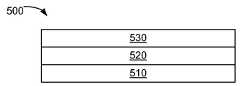
실시예들에서, RSM 셀은 STRAM 셀일 수 있다. STRAM 메모리 셀들은 MTJ(magnetic tunnel junction)를 포함하며, MTJ는 일반적으로 터널 장벽으로 또한 알려져 있는 얇은 절연층에 의해 분리된 2개의 자성 전극 층들을 포함한다. MTJ의 실시예는 도 5a에 도시된다. 도 5a에서의 MTJ(500)는 제 1 자성층(510) 및 제 2 자성층(530)을 포함하며, 제 1 자성층(510) 및 제 2 자성층(530)은 절연층(520)에 의해 분리된다. 제 1 자성층(510) 및 제 2 자성층(530)은 모두 독립적으로 다층 구조들일 수 있다. 도 5b는 제 1 전극층(540) 및 제 2 전극층(550)과 접촉하는 MTJ(500)를 도시한다. 제 1 전극층(540) 및 제 2 전극층(550)은 제 1 자성층(510) 및 제 2 자성층(530)을 자성층들을 통해 판독 및 기록 전류들을 제공하는 제어 회로(미도시)에 각각 전기적으로 접속시킨다. 제 1 자성층(510) 및 제 2 자성층(530)의 자화 벡터들의 상대적인 배향은 MTJ(500)에 걸친 저항에 의해 결정될 수 있으며; MTJ(500)에 걸친 저항은 제 1 자성층(510) 및 제 2 자성층(530)의 자화 벡터들의 상대적인 배향에 의해 결정될 수 있다.In embodiments, the RSM cell may be a STRAM cell. STRAM memory cells include a magnetic tunnel junction (MTJ), which includes two magnetic electrode layers separated by a thin insulating layer, also commonly known as a tunnel barrier. An embodiment of the MTJ is shown in Figure 5A. The
일반적으로, 제 1 자성층(510) 및 제 2 자성층(530)은 철(Fe), 코발트(Co), 및 니켈(Ni) 합금들과 같은 강자성 합금들로 이루어진다. 실시예들에서, 제 1 자성층(510) 및 제 2 자성층(530)은 FeMn, NiO, IrMn, PtPdMn, NiMn, 및 TbCo와 같은 합금들로 이루어질 수 있다. 일반적으로, 절연층(520)은 알루미늄 산화물(Al2O3) 또는 마그네슘 산화물(MgO)과 같은 절연 재료로 이루어진다.In general, the first
일반적으로, 자성층들 중 하나 예를 들어, 제 1 자성층(510)의 자화는 사전 결정된 방향으로 고정되는(pinned) 반면, 다른 자성층, 예를 들어 제 2 자성층(530)의 자화 방향은 스핀 토크의 영향 하에서 자유롭게 회전한다. 제 1 자성층(510)의 고정은 예를 들어, PtMn, IrMn, 및 그외의 재료들과 같은 반강자성 정렬된 재료에 의한 교환 바이어스(exchange bias)의 사용을 통해 달성될 수도 있다.Generally, one of the magnetic layers, for example, the magnetization of the first
특정 MTJ(500)는 제 1 전류가 제 2 자기층(530)(자유층)에서 제 1 자기층(510)(고정층)으로의 방향으로 메모리 셀을 통해 흐르게 함으로써 판독될 수 있다. MTJ(500)의 저항은 자유층이 고정층에 정렬되는지 또는 고정층의 반대로 정렬되는지에 따라 변할 수 있다. 이후, 저항에 의존하는 전압이 검출되고 기준 전압과 비교되어, MTJ가 정렬되는지 또는 반대로 정렬되는지 즉, "1"을 포함하는지 또는 "0"을 포함하는지를 결정할 수 있다. 특정 MTJ(500)는 제 2 전류(제 2 전류는 제 1 전류보다 큼)가 MTJ를 통과하게 함으로써 기록될 수 있다. 전류를 한 방향으로 통과시키는 것은 "1"을 기록할 것이고, 전류를 다른 방향으로 통과시키는 것은 "0"을 기록할 것이다. 여기에서 기재되는 스위칭 엘리먼트들의 양-방향 특성은 MTJ(500)를 통해 전류를 양 방향들로 흐르게 하는 능력을 제공할 수 있다.A
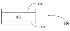
실시예들에서, RSM 셀은 RRAM 셀일 수 있다. 도 5c는 예시적인 저항 랜덤 액세스 메모리(RRAM) 셀(560)의 개략도이다. RRAM 셀(560)은 중간층(512)의 전기 저항을 변경함으로써 전류 또는 전압 펄스에 응답하는 중간층(512)을 포함한다. 이 현상은 전기 펄스 유도 저항 변화 효과라 지칭될 수 있다. 예를 들어, 이 효과는 메모리의 저항(즉, 데이터 상태)을 하나 이상의 고 저항 상태(들)로부터 저 저항 상태로 변화시킨다. 중간층(512)은 제 1 전극(514)과 제 2 전극(516) 사이에 삽입(interpose)되고, RRAM 셀의 데이터 저장 재료층으로서 동작한다. 제 1 전극(514) 및 제 2 전극(516)은 전압 소스(미도시)에 전기적으로 접속된다. 제 1 전극(514) 및 제 2 전극(516)은 예를 들어, 금속과 같은 임의의 유용한 전기 전도성 재료로 형성될 수 있다.In embodiments, the RSM cell may be an RRAM cell. FIG. 5C is a schematic diagram of an exemplary resistor Random Access Memory (RRAM)
중간층(512)을 형성하는 재료는 임의의 알려져 있는 유용한 RRAM 재료일 수 있다. 실시예들에서, 중간층(512)을 형성하는 재료는 금속 산화물과 같은 산화물 재료를 포함할 수 있다. 일부 실시예들에서, 금속 산화물은 바이너리(binary) 산화물 재료 또는 복합 금속 산화물 재료이다. 다른 실시예들에서, 중간층(512)을 형성하는 재료는 칼코게나이드 고체 전해질 재료(chalcogenide solid electrolyte material) 또는 유기/폴리머 재료를 포함할 수 있다.The material forming the
바이너리 금속 산화물 재료는 MxOy의 화학식으로서 표현될 수 있다. 이 식에서, "M", "O", "x", 및 "y"라는 문자들은 금속, 산소, 금속 조성비, 및 산소 조성비를 각각 지칭한다. 금속 "M"은 전이 금속 및/또는 알루미늄(Al)일 수도 있다. 이 경우, 전이 금속은 니켈(Ni), 니오븀(Nb), 티타늄(Ti), 지르코늄(Zr), 하프늄(Hf), 코발트(Co), 철(Fe), 구리(Cu), 및/또는 크롬(Cr)일 수도 있다. 중간층(512)으로서 사용될 수도 있는 바이너리 금속 산화물들의 구체적인 예들은 CuO, NiO, CoO, ZnO, CrO2, TiO2, HfO2, ZrO2, Fe2O3, 및 Nb2O5를 포함한다.The binary metal oxide material can be expressed as a chemical formula of Mx Oy . In this equation, the letters "M", "O", "x", and "y" refer to metal, oxygen, metal composition ratios, and oxygen composition ratios, respectively. The metal "M" may be a transition metal and / or aluminum (Al). In this case, the transition metal may be at least one selected from the group consisting of Ni, Nb, Ti, Zr, Hf, Co, Fe, Cu, (Cr). Specific examples of binary metal oxides which may be used as the
실시예들에서, 금속 산화물은 예를 들어, 식 Pr0.7Ca0.3MnO3, 또는 SrTiO3, 또는 SiZrO3, 또는 Cr 또는 Nb가 도핑된 이들 산화물들을 갖는 복합 산화물 재료와 같은 임의의 유용한 복합 금속 산화물일 수 있다. 또한, 복합물은 LaCuO4 또는 Bi2Sr2CaCu2O8을 포함할 수 있다. 고체 칼코게나이드 재료의 일례는 은(Ag) 성분을 함유하는 게르마늄-셀레나이드(GexSe100-x)이다. 유기 재료의 일례는 폴리(3,4-에틸렌다이옥시티오펜)(즉, PEDOT)이다.In embodiments, the metal oxide is, for example, expressionPr 0 .7 Ca 0 .3 MnO 3 , or SrTiO3, or SiZrO3, or Cr, or any material such as a composite oxide having an Nb-doped oxide thereof May be a useful composite metal oxide. Also, the composite may comprise LaCuO4 or Bi2 Sr2 CaCu2 O8 . An example of a solid chalcogenide material is germanium-selenide (Gex Se100-x ) containing a silver (Ag) component. An example of an organic material is poly (3,4-ethylenedioxythiophene) (i.e., PEDOT).
또한, RSM 셀은 납 지르콘산 티탄산염(lead zirconate titanate)("PZT"로 지칭됨) 또는 SrBi2Ta2O9("SBT"로 지칭됨)와 같은 재료들을 사용하여 도 5c와 유사한 구조들을 갖는 강유전성 캐패시터들을 포함할 수 있다. 이러한 메모리 셀들에서, 분극 방향을 스위칭하기 위해 전류가 사용될 수 있으며, 판독 전류는 분극이 업(up)인지 또는 다운(down)인지를 검출할 수 있다. 이러한 실시예들에서, 판독 동작은 파괴적인 프로세스이며, 여기서, 셀은 내부에 포함된 데이터를 손실하여, 그 셀에 데이터를 다시 기록하기 위해 리프레시를 요구할 것이다.The RSM cell can also be fabricated using materials such as lead zirconate titanate (referred to as "PZT") or SrBi2 Ta2 O9 (referred to as "SBT ≪ RTI ID = 0.0 > ferroelectric < / RTI > capacitors. In these memory cells, a current can be used to switch the polarization direction, and the read current can detect whether the polarization is up or down. In these embodiments, the read operation is a destructive process, where a cell will lose data contained therein and will require a refresh to rewrite the data to that cell.
기재되는 바와 같은 메모리 엘리먼트들은 상기 기재되는 바와 같은 스위칭 엘리먼트; 및 비활성 메모리 셀을 포함한다. 여기에서 기재되는 바와 같은 메모리 엘리먼트(600)의 예시적인 실시예가 도 6a에 도시된다. 상기 설명되고 예로 든 바와 같이, 메모리 엘리먼트(600)는 제 1 반도체층(650), 절연층(640), 제 2 반도체층(630), 제 1 금속 접촉부(660) 및 제 2 금속 접촉부(670)를 포함하는 스위칭 엘리먼트(615)를 포함한다. 메모리 셀(605)에 대한 공간 배향은 도면에 의해 제한되는 것으로 의미되지 않는다. 배향은 일반적으로 비활성 메모리 셀(605)이 금속 접촉부들 중 하나에 직렬로 전기적으로 접속됨을 도시하는 것으로만 의도된다(도 6a는 제 2 금속 접촉부(670)에 전기적으로 접속되는 비활성 메모리 셀(605)을 도시하지만, 물론 비활성 메모리 셀(605)은 제 1 금속 접촉부(660)에 전기적으로 접속될 수 있음).The memory elements as described include a switching element as described above; And an inert memory cell. An exemplary embodiment of a
도 6b는 비휘발성 메모리 엘리먼트의 컴포넌트들의 기능을 도시하는 회로도이다. 도 6b에 도시되는 바와 같이, 스위칭 엘리먼트(615)는 병렬인 2개의 개별 다이오드들(611 및 612)로서 기능을 한다. 이후, 스위칭 엘리먼트(615)는 저항기로서 기능을 하는 비활성 메모리 셀(605)에 직렬로 접속된다. 소스(680)에 의해 제공되는 전압은 VT1(도 1c 참조)보다 큰 전압을 제공할 수 있거나(이는 전류가 회로를 통해 한 방향으로 흐르게 함), VT2(도 1c 참조)보다 적은 전압을 제공할 수 있다(이는 전류가 회로를 통해 다른 방향으로 흐르게 함). 2개의 경로들은 비휘발성 메모리 셀(605)의 저항 상태를 결정하는 단계를 포함하여, 다양한 동작들이 비활성 메모리 셀(605) 상에서 수행되게 할 수 있다.6B is a circuit diagram showing the function of the components of the non-volatile memory element. 6B, the switching
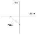
여기에서 기재되는 바와 같은 메모리 엘리먼트들은 메모리 어레이들에서 이용될 수 있다. 실시예들에서, 여기에서 기재되는 바와 같은 메모리 엘리먼트들은 크로스바 메모리 어레이들에서 이용될 수 있다. 크로스바 메모리 어레이의 예시적인 도면은 도 7a에 도시된다. 예시적인 크로스바 메모리 어레이는 대략 병렬인 컨덕터들(704)의 제 2 층이 위에 놓이거나(또는 아래에 놓인) 대략 병렬인 컨덕터들(702)의 제 1 층을 포함한다. 실시예들에서, 제 2 층(704)의 컨덕터들은 배향이 제 1 층(702)의 컨덕터들과 실질적으로 수직할 수 있다. 실시예들에서, 층들 사이의 배향 각은 직각이 아닐 수도 있다. 컨덕터들의 2개의 층들은 격자 또는 크로스바를 형성하며, 제 2 층(704)의 각각의 컨덕터는 제 1 층(702)의 컨덕터들 모두의 위에 놓이며, 2개의 컨덕터들 사이의 가장 가까운 접촉을 나타내는 컨덕터 교차점들에서 제 1 층(702)의 각각의 컨덕터와 가깝게 접촉한다. 도 7a의 개별 컨덕터들이 사각 단면들을 갖는 것으로 도시되지만, 컨덕터들은 또한 정사각형, 원형, 타원형, 또는 임의의 다른 일정한 또는 일정하지 않은 단면들을 가질 수 있다. 또한, 컨덕터들은 많은 상이한 폭들 또는 지름들, 및 형상비들 또는 이심률(eccentricity)들을 가질 수 있다.Memory elements such as those described herein may be used in memory arrays. In embodiments, memory elements as described herein may be used in crossbar memory arrays. An exemplary diagram of a crossbar memory array is shown in FIG. 7A. The exemplary crossbar memory array includes a first layer of
상기 기재되는 바와 같은 메모리 엘리먼트들은 크로스바 메모리 어레이들의 컨덕터 교차점들 중 적어도 일부에 배치될 수 있다. 실시예들에서, 기재된 메모리 엘리먼트들은 컨덕터 교차점들의 실질적으로 모두에 배치될 수 있다. 기재되는 메모리 엘리먼트들에 의해 접속되는 컨덕터 교차점은 "크로스바 접합"으로 지칭될 수 있다. 도 7b 및 7c는 크로스바 메모리 어레이 내에서 2개의 인접한 층들의 컨덕터들(702a 및 704a)을 상호접속시키는 크로스바 접합의 2개의 상이한 도면들을 제공한다. 크로스바 접합은 2개의 컨덕터들(702a 및 704a) 사이의 물리적 접촉을 포함할 수 있거나, 포함하지 않을 수 있다. 도 7b에 도시되는 바와 같이, 2개의 컨덕터들은 그들의 오버랩 지점에서 물리적으로 접촉하지 않지만, 컨덕터들(702a 및 704a) 사이의 갭은 그들의 가장 가까운 오버랩 지점에서 2개의 컨덕터들 사이에 놓이는 메모리 엘리먼트(706a)에 의해 걸쳐진다. 도 7c는 도 7b에 도시되는 메모리 엘리먼트(706a) 및 오버래핑 컨덕터들(702a 및 704a)의 개략 대표도를 도시한다.The memory elements as described above may be placed in at least a portion of the conductor intersections of the crossbar memory arrays. In embodiments, the described memory elements may be disposed on substantially all of the conductor intersections. The conductor junctions connected by the memory elements described may be referred to as "crossbar junctions. &Quot; 7b and 7c provide two different views of a crossbar
메모리 엘리먼트들에 포함되는 스위칭 디바이스들이 누설 전류들로 인하여 동작들을 판독, 기록 및 삭제하는 동안 의도하지 않은 셀들에 대한 교란(disturbance)들을 회피하거나 최소화할 수 있는 집적된 선택적 엘리먼트로서 기능을 할 수 있기 때문에, 기재되는 메모리 엘리먼트들은 크로스바 메모리 어레이들에서 유리하게 이용될 수 있다. STRAM이 동작들의 기록 및 삭제가 반대 극성들을 사용하여 수행되도록 요구하기 때문에, 여기에서 기재되는 스위칭 디바이스들은 STRAM과 결합하여 특히 유리하다.The switching devices included in the memory elements can function as an integrated optional element that can avoid or minimize disturbances to unintended cells while reading, writing and erasing operations due to leakage currents Thus, the memory elements described can be advantageously used in crossbar memory arrays. The switching devices described herein are particularly advantageous in combination with STRAM, since the STRAM requires that the recording and erasing of operations be performed using the opposite polarities.
따라서, 쇼트키 다이오드 스위치 및 이를 포함하는 메모리 유닛들의 실시예들이 기재된다. 상기 설명된 구현들 및 다른 구현들은 다음의 청구항들의 범위 내에 존재한다. 당업자는 본 발명이 기재된 실시예들 이외의 실시예들로 실시될 수 있다는 것을 인식할 것이다. 기재된 실시예들은 제한이 아닌 예시를 위해서 제시되고, 본 개시는 다음의 청구항들에 의해서만 제한된다.
Accordingly, embodiments of a Schottky diode switch and memory units comprising the same are described. The above-described implementations and other implementations are within the scope of the following claims. Those skilled in the art will recognize that the invention may be practiced in other embodiments than the described embodiments. The described embodiments are presented for purposes of illustration and not limitation, and the disclosure is limited only by the following claims.
Claims (20)
Translated fromKorean제 1 반도체층, 절연층 및 제 2 반도체층을 포함하는 적층 물품(layered article)을 제공하는 단계;
상기 적층 물품의 제 1 부분만을 보호하는 제 1 마스크 영역을 형성하는 단계;
제 1 에너지 레벨을 사용하여 상기 제 2 반도체층의 제 2 부분만을 도핑하는 단계;
상기 적층 물품의 제 3 부분만을 보호하는 제 2 마스크 영역을 형성하는 단계 ― 상기 적층 물품의 제 1 부분 및 제 3 부분은 단지 부분적으로만 오버랩함 ― ;
제 2 에너지 레벨을 사용하여 상기 제 1 반도체층의 제 4 부분만을 도핑하는 단계 ― 상기 제 1 에너지 레벨 및 상기 제 2 에너지 레벨은 상이하고, 이로써 도핑된 적층 물품을 형성함 ― ;
상기 도핑된 적층 물품의 일부 상에서만 접촉 마스크를 형성하는 단계;
적어도 상기 제 2 반도체층, 상기 절연층 및 상기 제 1 반도체층 중 일부를 에칭하는 단계; 및
상기 제 2 반도체층, 상기 절연층 및 상기 제 1 반도체층의 에칭된 영역들에서 제 1 금속 접촉부 및 제 2 금속 접촉부를 형성하는 단계를 포함하는,
스위칭 엘리먼트를 형성하는 방법.A method of forming a switching element,
Providing a layered article comprising a first semiconductor layer, an insulating layer and a second semiconductor layer;
Forming a first mask region that protects only the first portion of the stacked article;
Doping only the second portion of the second semiconductor layer using a first energy level;
Forming a second mask region that protects only the third portion of the stacked article, wherein the first and third portions of the stacked article overlap only partially;
Doping only the fourth portion of the first semiconductor layer using a second energy level, the first energy level and the second energy level being different, thereby forming a doped laminated article;
Forming a contact mask only on a portion of the doped laminated article;
Etching at least a portion of the second semiconductor layer, the insulating layer and the first semiconductor layer; And
And forming a first metal contact and a second metal contact in etched regions of the second semiconductor layer, the insulating layer, and the first semiconductor layer.
/ RTI >
상기 제 1 에너지는 상기 제 2 에너지보다 작은,
스위칭 엘리먼트를 형성하는 방법.The method according to claim 1,
Wherein the first energy is less than the second energy,
/ RTI >
상기 적층 물품을 제공하는 단계는,
제 1 기판, 제 2 절연층 및 상기 제 1 반도체층을 포함하는 제 1 적층 구조를 제공하는 단계 ― 상기 제 2 절연층은 상기 제 1 기판과 상기 제 1 반도체층 사이에 위치됨 ― ;
상기 절연층 및 상기 제 2 반도체층을 포함하는 제 2 적층 구조를 제공하는 단계; 및
상기 제 2 적층 구조의 상기 절연층이 상기 제 1 적층 구조의 상기 제 1 반도체층에 인접하도록 상기 제 2 적층 구조를 상기 제 1 적층 구조와 접촉하게 배치하며, 상기 적층 물품을 형성하기 위해서 상기 제 1 적층 구조를 상기 제 2 적층 구조에 본딩(bond)하는 단계를 포함하는,
스위칭 엘리먼트를 형성하는 방법.The method according to claim 1,
Wherein providing the laminated article comprises:
Providing a first laminate structure comprising a first substrate, a second insulating layer and the first semiconductor layer, the second insulating layer being positioned between the first substrate and the first semiconductor layer;
Providing a second stack structure including the insulating layer and the second semiconductor layer; And
The second laminate structure is disposed in contact with the first laminate structure such that the insulating layer of the second laminate structure is adjacent to the first semiconductor layer of the first laminate structure, Lt; RTI ID = 0.0 > 1 < / RTI > laminate structure to the second laminate structure.
/ RTI >
상기 제 2 적층 구조는 실리콘 웨이퍼를 산화시킴으로써 적어도 부분적으로 형성되는,
스위칭 엘리먼트를 형성하는 방법.The method of claim 3,
Wherein the second laminate structure is at least partially formed by oxidizing a silicon wafer,
/ RTI >
상기 제 2 적층 구조는 실리콘 웨이퍼 상에 절연 재료를 증착시킴으로써 적어도 부분적으로 형성되는,
스위칭 엘리먼트를 형성하는 방법.The method of claim 3,
Wherein the second laminate structure is at least partially formed by depositing an insulating material on a silicon wafer,
/ RTI >
상기 제 1 마스크 영역 및 상기 제 2 마스크 영역은 상기 적층 물품의 일부를 도핑되지 않은 상태로 남기도록 구성되는,
스위칭 엘리먼트를 형성하는 방법.The method according to claim 1,
Wherein the first mask region and the second mask region are configured to leave a portion of the laminated article in an undoped state,
/ RTI >
상기 적층 물품의 도핑되지 않은 부분은 상기 접촉 마스크에 의해 마스킹된 상기 도핑된 적층 물품의 일부와 일치하는,
스위칭 엘리먼트를 형성하는 방법.The method according to claim 6,
Wherein an undoped portion of the laminated article coincides with a portion of the doped laminated article masked by the contact mask,
/ RTI >
제 1 반도체층, 제 2 반도체층, 및 상기 제 1 반도체층과 상기 제 2 반도체층 사이에 위치된 절연층을 포함하는 적층 물품(layered article)을 제공하는 단계;
제 1 에너지 레벨을 사용하여 상기 제 2 반도체층의 일부만을 도핑하는 단계;
제 2 에너지 레벨을 사용하여 상기 제 1 반도체층의 일부만을 도핑하는 단계― 상기 제 1 에너지 레벨 및 상기 제 2 에너지 레벨은 상이하고, 이로써 도핑된 적층 물품을 형성함 ―;
상기 도핑된 적층 물품의 일부 상에서만 접촉 마스크를 형성하는 단계;
적어도 상기 제 2 반도체층, 상기 절연층 및 상기 제 1 반도체층 중 일부를 에칭하는 단계; 및
상기 제 2 반도체층, 상기 절연층 및 상기 제 1 반도체층의 에칭된 영역들에서 제 1 금속 접촉부 및 제 2 금속 접촉부를 형성하는 단계를 포함하는,
스위칭 엘리먼트를 형성하는 방법.A method of forming a switching element,
Providing a layered article comprising a first semiconductor layer, a second semiconductor layer, and an insulating layer positioned between the first semiconductor layer and the second semiconductor layer;
Doping only a portion of the second semiconductor layer using a first energy level;
Doping only a portion of the first semiconductor layer using a second energy level, the first energy level and the second energy level being different, thereby forming a doped laminated article;
Forming a contact mask only on a portion of the doped laminated article;
Etching at least a portion of the second semiconductor layer, the insulating layer and the first semiconductor layer; And
And forming a first metal contact and a second metal contact in etched regions of the second semiconductor layer, the insulating layer, and the first semiconductor layer.
/ RTI >
상기 제 2 반도체층의 일부만을 도핑하는 단계는 제 1 마스크 영역을 형성하는 단계를 포함하고, 상기 마스크 영역은 산화 재료들, 실리콘 질화물들 또는 포토레지스트를 포함하는,
스위칭 엘리먼트를 형성하는 방법.9. The method of claim 8,
Wherein the step of doping only a portion of the second semiconductor layer comprises forming a first mask region, the mask region comprising oxidation materials, silicon nitrides or photoresist,
/ RTI >
상기 제 1 반도체층의 일부만을 도핑하는 단계는 제 3 마스크 영역을 형성하는 단계를 포함하고, 상기 마스크 영역은 산화 재료들, 실리콘 질화물들 또는 포토레지스트를 포함하는,
스위칭 엘리먼트를 형성하는 방법.9. The method of claim 8,
Wherein the step of doping only a portion of the first semiconductor layer comprises forming a third mask region, wherein the mask region comprises oxide materials, silicon nitrides or photoresist,
/ RTI >
상기 적층 물품을 제공하는 단계는,
제 1 기판, 제 2 절연층 및 상기 제 1 반도체층을 포함하는 제 1 적층 구조를 제공하는 단계 ― 상기 제 2 절연층은 상기 제 1 기판과 상기 제 1 반도체층 사이에 위치됨 ― ;
상기 절연층 및 상기 제 2 반도체층을 포함하는 제 2 적층 구조를 제공하는 단계; 및
상기 제 2 적층 구조의 상기 절연층이 상기 제 1 적층 구조의 상기 제 1 반도체층에 인접하도록 상기 제 2 적층 구조를 상기 제 1 적층 구조와 접촉하게 배치하며, 상기 적층 물품을 형성하기 위해서 상기 제 1 적층 구조를 상기 제 2 적층 구조에 본딩(bond)하는 단계를 포함하는,
스위칭 엘리먼트를 형성하는 방법.9. The method of claim 8,
Wherein providing the laminated article comprises:
Providing a first laminate structure comprising a first substrate, a second insulating layer and the first semiconductor layer, the second insulating layer being positioned between the first substrate and the first semiconductor layer;
Providing a second stack structure including the insulating layer and the second semiconductor layer; And
The second laminate structure is disposed in contact with the first laminate structure such that the insulating layer of the second laminate structure is adjacent to the first semiconductor layer of the first laminate structure, Lt; RTI ID = 0.0 > 1 < / RTI > laminate structure to the second laminate structure.
/ RTI >
상기 제 2 적층 구조는 실리콘 웨이퍼를 산화시킴으로써 적어도 부분적으로 형성되는,
스위칭 엘리먼트를 형성하는 방법.12. The method of claim 11,
Wherein the second laminate structure is at least partially formed by oxidizing a silicon wafer,
/ RTI >
상기 제 2 적층 구조는 실리콘 웨이퍼 상에 절연 재료를 증착시킴으로써 적어도 부분적으로 형성되는,
스위칭 엘리먼트를 형성하는 방법.12. The method of claim 11,
Wherein the second laminate structure is at least partially formed by depositing an insulating material on a silicon wafer,
/ RTI >
상기 제 1 마스크 영역은 상기 적층 물품의 일부를 도핑되지 않은 상태로 남기도록 구성되는,
스위칭 엘리먼트를 형성하는 방법.10. The method of claim 9,
Wherein the first mask region is configured to leave a portion of the laminated article in an undoped state,
/ RTI >
상기 적층 물품의 도핑되지 않은 부분은 상기 접촉 마스크에 의해 마스킹된 상기 도핑된 적층 물품의 일부와 일치하는,
스위칭 엘리먼트를 형성하는 방법.12. The method of claim 11,
Wherein an undoped portion of the laminated article coincides with a portion of the doped laminated article masked by the contact mask,
/ RTI >
상기 제 1 에너지는 상기 제 2 에너지보다 작은,
스위칭 엘리먼트를 형성하는 방법.9. The method of claim 8,
Wherein the first energy is less than the second energy,
/ RTI >
제 1 기판, 제 2 절연층 및 제 1 반도체층을 포함하는 제 1 적층 구조를 제공하는 단계 ― 상기 제 2 절연층은 상기 제 1 기판과 상기 제 1 반도체층 사이에 위치됨 ― ;
절연층 및 제 2 반도체층을 포함하는 제 2 적층 구조를 제공하는 단계;
상기 제 2 적층 구조의 상기 절연층이 상기 제 1 적층 구조의 상기 제 1 반도체층에 인접하도록 상기 제 2 적층 구조를 상기 제 1 적층 구조와 접촉하게 배치하며, 상기 적층 물품을 형성하기 위해서 상기 제 1 적층 구조를 상기 제 2 적층 구조에 본딩(bond)하는 단계;
상기 적층 물품의 제 1 부분만을 보호하는 제 1 마스크 영역을 형성하는 단계;
제 1 에너지 레벨을 사용하여 상기 제 2 반도체층의 제 2 부분만을 도핑하는 단계;
상기 적층 물품의 제 3 부분만을 보호하는 제 2 마스크 영역을 형성하는 단계 ― 상기 적층 물품의 제 1 부분 및 제 3 부분은 단지 부분적으로만 오버랩함 ― ;
제 2 에너지 레벨을 사용하여 상기 제 1 반도체층의 제 4 부분만을 도핑하는 단계 ― 상기 제 1 에너지 레벨 및 상기 제 2 에너지 레벨은 상이하고, 이로써 도핑된 적층 물품을 형성함 ― ;
상기 도핑된 적층 물품의 일부 상에서만 접촉 마스크를 형성하는 단계;
적어도 상기 제 2 반도체층, 상기 절연층 및 상기 제 1 반도체층 중 일부를 에칭하는 단계; 및
상기 제 2 반도체층, 상기 절연층 및 상기 제 1 반도체층의 에칭된 영역들에서 제 1 금속 접촉부 및 제 2 금속 접촉부를 형성하는 단계를 포함하는,
스위칭 엘리먼트를 형성하는 방법.A method of forming a switching element,
Providing a first laminate structure comprising a first substrate, a second insulating layer and a first semiconductor layer, the second insulating layer being positioned between the first substrate and the first semiconductor layer;
Providing a second laminate structure comprising an insulating layer and a second semiconductor layer;
The second laminate structure is disposed in contact with the first laminate structure such that the insulating layer of the second laminate structure is adjacent to the first semiconductor layer of the first laminate structure, 1 bonding a laminate structure to the second laminate structure;
Forming a first mask region that protects only the first portion of the stacked article;
Doping only the second portion of the second semiconductor layer using a first energy level;
Forming a second mask region that protects only the third portion of the stacked article, wherein the first and third portions of the stacked article overlap only partially;
Doping only the fourth portion of the first semiconductor layer using a second energy level, the first energy level and the second energy level being different, thereby forming a doped laminated article;
Forming a contact mask only on a portion of the doped laminated article;
Etching at least a portion of the second semiconductor layer, the insulating layer and the first semiconductor layer; And
And forming a first metal contact and a second metal contact in etched regions of the second semiconductor layer, the insulating layer, and the first semiconductor layer.
/ RTI >
상기 제 1 에너지는 상기 제 2 에너지보다 작은,
스위칭 엘리먼트를 형성하는 방법.18. The method of claim 17,
Wherein the first energy is less than the second energy,
/ RTI >
상기 제 1 마스크 영역 및 상기 제 2 마스크 영역은 상기 적층 물품의 일부를 도핑되지 않은 상태로 남기도록 구성되는,
스위칭 엘리먼트를 형성하는 방법.18. The method of claim 17,
Wherein the first mask region and the second mask region are configured to leave a portion of the laminated article in an undoped state,
/ RTI >
상기 적층 물품의 도핑되지 않은 부분은 상기 접촉 마스크에 의해 마스킹된 상기 도핑된 적층 물품의 일부와 일치하는,
스위칭 엘리먼트를 형성하는 방법.18. The method of claim 17,
Wherein an undoped portion of the laminated article coincides with a portion of the doped laminated article masked by the contact mask,
/ RTI >
Applications Claiming Priority (3)
| Application Number | Priority Date | Filing Date | Title |
|---|---|---|---|
| US12/502,221US8158964B2 (en) | 2009-07-13 | 2009-07-13 | Schottky diode switch and memory units containing the same |
| US12/502,221 | 2009-07-13 | ||
| PCT/US2010/041539WO2011008650A1 (en) | 2009-07-13 | 2010-07-09 | Schottky diode switch and memory units containing the same |
Related Parent Applications (1)
| Application Number | Title | Priority Date | Filing Date |
|---|---|---|---|
| KR1020127003805ADivisionKR101368313B1 (en) | 2009-07-13 | 2010-07-09 | Schottky diode switch and memory units containing the same |
Publications (2)
| Publication Number | Publication Date |
|---|---|
| KR20130099224A KR20130099224A (en) | 2013-09-05 |
| KR101444912B1true KR101444912B1 (en) | 2014-09-26 |
Family
ID=42668036
Family Applications (3)
| Application Number | Title | Priority Date | Filing Date |
|---|---|---|---|
| KR1020137019955AExpired - Fee RelatedKR101444912B1 (en) | 2009-07-13 | 2010-07-09 | Schottky diode switch and memory units containing the same |
| KR1020137019964AExpired - Fee RelatedKR101412190B1 (en) | 2009-07-13 | 2010-07-09 | Schottky diode switch and memory units containing the same |
| KR1020127003805AExpired - Fee RelatedKR101368313B1 (en) | 2009-07-13 | 2010-07-09 | Schottky diode switch and memory units containing the same |
Family Applications After (2)
| Application Number | Title | Priority Date | Filing Date |
|---|---|---|---|
| KR1020137019964AExpired - Fee RelatedKR101412190B1 (en) | 2009-07-13 | 2010-07-09 | Schottky diode switch and memory units containing the same |
| KR1020127003805AExpired - Fee RelatedKR101368313B1 (en) | 2009-07-13 | 2010-07-09 | Schottky diode switch and memory units containing the same |
Country Status (5)
| Country | Link |
|---|---|
| US (3) | US8158964B2 (en) |
| JP (1) | JP5702381B2 (en) |
| KR (3) | KR101444912B1 (en) |
| CN (1) | CN102473706B (en) |
| WO (1) | WO2011008650A1 (en) |
Families Citing this family (18)
| Publication number | Priority date | Publication date | Assignee | Title |
|---|---|---|---|---|
| JP5381420B2 (en)* | 2008-07-22 | 2014-01-08 | 富士電機株式会社 | Semiconductor device |
| CN102610749B (en)* | 2011-01-25 | 2014-01-29 | 中国科学院微电子研究所 | Resistive random access memory cell and memory |
| US8879314B2 (en)* | 2011-06-06 | 2014-11-04 | Iii Holdings 1, Llc | Memory cell with Schottky diode |
| US9349445B2 (en) | 2011-09-16 | 2016-05-24 | Micron Technology, Inc. | Select devices for memory cell applications |
| US8780607B2 (en) | 2011-09-16 | 2014-07-15 | Micron Technology, Inc. | Select devices for memory cell applications |
| US9142767B2 (en)* | 2011-09-16 | 2015-09-22 | Micron Technology, Inc. | Resistive memory cell including integrated select device and storage element |
| US8691324B2 (en) | 2012-04-03 | 2014-04-08 | Xerox Corporation | Dry coating processes for substrates |
| US9853053B2 (en) | 2012-09-10 | 2017-12-26 | 3B Technologies, Inc. | Three dimension integrated circuits employing thin film transistors |
| US8828785B2 (en)* | 2012-09-12 | 2014-09-09 | International Business Machines Corporation | Single-crystal phase change material on insulator for reduced cell variability |
| US20150179930A1 (en)* | 2013-12-23 | 2015-06-25 | Intermolecular Inc. | Schottky Barriers for Resistive Random Access Memory Cells |
| BR112016016577B1 (en)* | 2014-01-24 | 2021-05-04 | Hi-Lex Corporation | method for producing titanium powder containing a solid solubilized nitrogen |
| WO2016099580A2 (en) | 2014-12-23 | 2016-06-23 | Lupino James John | Three dimensional integrated circuits employing thin film transistors |
| KR101959378B1 (en)* | 2016-08-26 | 2019-03-19 | 한국과학기술연구원 | Manufacturing method for ⅲ-ⅴ compound semiconductor device and semiconductor device thereto |
| DE102017001963A1 (en) | 2017-03-01 | 2018-09-06 | Forschungsverbund Berlin E.V. | Tunnel resistance device and method for its manufacture |
| KR102226206B1 (en)* | 2020-02-06 | 2021-03-11 | 포항공과대학교 산학협력단 | Memory device including double PN junctions and driving method thereof |
| KR102358352B1 (en)* | 2020-06-23 | 2022-02-03 | 국민대학교산학협력단 | Modeling method and apparatus for memristor device |
| FR3117258B1 (en)* | 2020-12-07 | 2023-12-22 | Commissariat Energie Atomique | SELECTOR DEVICE, RESISTIVE TYPE MEMORY DEVICE AND ASSOCIATED MANUFACTURING METHOD |
| CN120391092A (en)* | 2022-12-19 | 2025-07-29 | 凌北卿 | Semiconductor structure and memory device and method of manufacturing the same |
Citations (4)
| Publication number | Priority date | Publication date | Assignee | Title |
|---|---|---|---|---|
| US5341114A (en)* | 1990-11-02 | 1994-08-23 | Ail Systems, Inc. | Integrated limiter and amplifying devices |
| US20030089959A1 (en) | 2001-09-25 | 2003-05-15 | Sanyo Electric Company, Ltd. | Schottky barrier diode |
| US20060076548A1 (en) | 2004-10-08 | 2006-04-13 | Samsung Electronics Co., Ltd. | PRAMs having a plurality of active regions located vertically in sequence and methods of forming the same |
| US20080180989A1 (en) | 2007-01-30 | 2008-07-31 | In-Gyu Baek | Memory devices including multi-bit memory cells having magnetic and resistive memory elements and related methods |
Family Cites Families (174)
| Publication number | Priority date | Publication date | Assignee | Title |
|---|---|---|---|---|
| US3746945A (en)* | 1971-10-27 | 1973-07-17 | Motorola Inc | Schottky diode clipper device |
| US3982233A (en) | 1974-02-19 | 1976-09-21 | Ampex Corporation | Core memory with improved sense-inhibit recovery time |
| GB1507061A (en) | 1974-03-26 | 1978-04-12 | Signetics Corp | Semiconductors |
| US3982235A (en) | 1974-08-28 | 1976-09-21 | The United States Of America As Represented By The Secretary Of The Navy | Sinusoidal film plated memory wire |
| US4110488A (en) | 1976-04-09 | 1978-08-29 | Rca Corporation | Method for making schottky barrier diodes |
| US4056642A (en) | 1976-05-14 | 1977-11-01 | Data General Corporation | Method of fabricating metal-semiconductor interfaces |
| US4247915A (en) | 1979-01-02 | 1981-01-27 | Texas Instruments Incorporated | Punch-through load devices in high density static memory cell |
| US4232057A (en) | 1979-03-01 | 1980-11-04 | International Business Machines Corporation | Semiconductor plasma oxidation |
| US4323589A (en) | 1980-05-07 | 1982-04-06 | International Business Machines Corporation | Plasma oxidation |
| JPS6173345A (en) | 1984-09-19 | 1986-04-15 | Toshiba Corp | semiconductor equipment |
| US4576829A (en) | 1984-12-28 | 1986-03-18 | Rca Corporation | Low temperature growth of silicon dioxide on silicon |
| JPS62289544A (en) | 1986-06-09 | 1987-12-16 | Daikin Ind Ltd | Fluorine-containing compound |
| JPH0766965B2 (en) | 1987-02-27 | 1995-07-19 | 株式会社東芝 | Semiconductor device and manufacturing method thereof |
| EP0935255A2 (en) | 1989-04-13 | 1999-08-11 | SanDisk Corporation | Flash EEPROM system |
| US5083190A (en) | 1989-09-05 | 1992-01-21 | Motorola, Inc. | Shared gate CMOS transistor |
| US5278636A (en) | 1989-09-29 | 1994-01-11 | The United States Of America As Represented By The Administrator Of The National Aeronautics And Space Administration | Non-volatile, solid state bistable electrical switch |
| US5135878A (en) | 1990-08-28 | 1992-08-04 | Solid State Devices, Inc. | Schottky diode |
| JPH07118522B2 (en) | 1990-10-24 | 1995-12-18 | インターナショナル・ビジネス・マシーンズ・コーポレイション | Method and semiconductor structure for oxidizing a substrate surface |
| EP0488677A3 (en) | 1990-11-29 | 1992-08-26 | Kawasaki Steel Corporation | Semiconductor device of band-to-band tunneling type |
| TW261687B (en) | 1991-11-26 | 1995-11-01 | Hitachi Seisakusyo Kk | |
| US5926412A (en) | 1992-02-09 | 1999-07-20 | Raytheon Company | Ferroelectric memory structure |
| KR100305123B1 (en) | 1992-12-11 | 2001-11-22 | 비센트 비.인그라시아, 알크 엠 아헨 | Static Random Access Memory Cells and Semiconductor Devices Containing These |
| JPH06196683A (en)* | 1992-12-22 | 1994-07-15 | Hitachi Ltd | Schottky barrier diode and semiconductor integrated circuit device |
| US5913149A (en) | 1992-12-31 | 1999-06-15 | Micron Technology, Inc. | Method for fabricating stacked layer silicon nitride for low leakage and high capacitance |
| US5443863A (en) | 1994-03-16 | 1995-08-22 | Auburn University | Low-temperature oxidation at surfaces using ozone decomposition products formed by microwave discharge |
| DE69517700T2 (en) | 1994-11-04 | 2000-11-23 | Micron Technology, Inc. | ARMING PROCEDURE FOR EMISSION POINTS THROUGH OXYDATION AT LOW TEMPERATURE |
| US5580804A (en) | 1994-12-15 | 1996-12-03 | Advanced Micro Devices, Inc. | Method for fabricating true LDD devices in a MOS technology |
| US5872052A (en) | 1996-02-12 | 1999-02-16 | Micron Technology, Inc. | Planarization using plasma oxidized amorphous silicon |
| US5614430A (en) | 1996-03-11 | 1997-03-25 | Taiwan Semiconductor Manufacturing Company Ltd. | Anti-punchthrough ion implantation for sub-half micron channel length MOSFET devices |
| US8018058B2 (en) | 2004-06-21 | 2011-09-13 | Besang Inc. | Semiconductor memory device |
| US7800199B2 (en) | 2003-06-24 | 2010-09-21 | Oh Choonsik | Semiconductor circuit |
| US7888764B2 (en) | 2003-06-24 | 2011-02-15 | Sang-Yun Lee | Three-dimensional integrated circuit structure |
| US7470142B2 (en) | 2004-06-21 | 2008-12-30 | Sang-Yun Lee | Wafer bonding method |
| US7052941B2 (en) | 2003-06-24 | 2006-05-30 | Sang-Yun Lee | Method for making a three-dimensional integrated circuit structure |
| US7470598B2 (en) | 2004-06-21 | 2008-12-30 | Sang-Yun Lee | Semiconductor layer structure and method of making the same |
| US20050280155A1 (en) | 2004-06-21 | 2005-12-22 | Sang-Yun Lee | Semiconductor bonding and layer transfer method |
| US8779597B2 (en) | 2004-06-21 | 2014-07-15 | Sang-Yun Lee | Semiconductor device with base support structure |
| US7633162B2 (en) | 2004-06-21 | 2009-12-15 | Sang-Yun Lee | Electronic circuit with embedded memory |
| KR100304161B1 (en) | 1996-12-18 | 2001-11-30 | 미다라이 후지오 | Manufacturing method of semiconductor member |
| US6034389A (en) | 1997-01-22 | 2000-03-07 | International Business Machines Corporation | Self-aligned diffused source vertical transistors with deep trench capacitors in a 4F-square memory cell array |
| US5929477A (en) | 1997-01-22 | 1999-07-27 | International Business Machines Corporation | Self-aligned diffused source vertical transistors with stack capacitors in a 4F-square memory cell array |
| US6121654A (en) | 1997-10-10 | 2000-09-19 | The Research Foundation Of State University Of New York | Memory device having a crested tunnel barrier |
| JP3379062B2 (en) | 1997-12-02 | 2003-02-17 | 富士通カンタムデバイス株式会社 | Semiconductor device and manufacturing method thereof |
| NZ505840A (en) | 1997-12-17 | 2004-12-24 | B & R Ind Pty Ltd | Container made from a preform blown in a two stage process where a handle is integrally affixed at separate points of connection to the preform |
| JPH11186568A (en)* | 1997-12-25 | 1999-07-09 | Fuji Electric Co Ltd | High breakdown voltage diode and method of manufacturing the same |
| US6043527A (en) | 1998-04-14 | 2000-03-28 | Micron Technology, Inc. | Circuits and methods for a memory cell with a trench plate trench capacitor and a vertical bipolar read device |
| US6165834A (en) | 1998-05-07 | 2000-12-26 | Micron Technology, Inc. | Method of forming capacitors, method of processing dielectric layers, method of forming a DRAM cell |
| US6121642A (en) | 1998-07-20 | 2000-09-19 | International Business Machines Corporation | Junction mott transition field effect transistor (JMTFET) and switch for logic and memory applications |
| US20040017721A1 (en) | 1998-10-30 | 2004-01-29 | Schwabe Nikolai Franz Gregoe | Magnetic storage device |
| US6300205B1 (en) | 1998-11-18 | 2001-10-09 | Advanced Micro Devices, Inc. | Method of making a semiconductor device with self-aligned active, lightly-doped drain, and halo regions |
| US6114211A (en) | 1998-11-18 | 2000-09-05 | Advanced Micro Devices, Inc. | Semiconductor device with vertical halo region and methods of manufacture |
| JP2000223683A (en) | 1999-02-02 | 2000-08-11 | Canon Inc | Composite member and its separation method, bonded substrate and its separation method, transfer layer transfer method, and SOI substrate manufacturing method |
| US6448840B2 (en) | 1999-11-30 | 2002-09-10 | Intel Corporation | Adaptive body biasing circuit and method |
| US6617642B1 (en) | 2000-02-23 | 2003-09-09 | Tripath Technology, Inc. | Field effect transistor structure for driving inductive loads |
| US6518609B1 (en) | 2000-08-31 | 2003-02-11 | University Of Maryland | Niobium or vanadium substituted strontium titanate barrier intermediate a silicon underlayer and a functional metal oxide film |
| FR2815961B1 (en)* | 2000-10-26 | 2008-11-28 | Centre Nat Rech Scient | NEW INTERMEDIATES USEFUL FOR RETINOID SYNTHESIS |
| US6850397B2 (en) | 2000-11-06 | 2005-02-01 | Sarnoff Corporation | Silicon controlled rectifier electrostatic discharge protection device for power supply lines with powerdown mode of operation |
| US6346477B1 (en) | 2001-01-09 | 2002-02-12 | Research Foundation Of Suny - New York | Method of interlayer mediated epitaxy of cobalt silicide from low temperature chemical vapor deposition of cobalt |
| US6515345B2 (en) | 2001-02-21 | 2003-02-04 | Semiconductor Components Industries Llc | Transient voltage suppressor with diode overlaying another diode for conserving space |
| US6618295B2 (en) | 2001-03-21 | 2003-09-09 | Matrix Semiconductor, Inc. | Method and apparatus for biasing selected and unselected array lines when writing a memory array |
| US6462359B1 (en) | 2001-03-22 | 2002-10-08 | T-Ram, Inc. | Stability in thyristor-based memory device |
| JP4198469B2 (en) | 2001-04-11 | 2008-12-17 | シリコン・セミコンダクター・コーポレイション | Power device and manufacturing method thereof |
| JP5019681B2 (en) | 2001-04-26 | 2012-09-05 | ルネサスエレクトロニクス株式会社 | Thin film magnetic memory device |
| US7476925B2 (en) | 2001-08-30 | 2009-01-13 | Micron Technology, Inc. | Atomic layer deposition of metal oxide and/or low asymmetrical tunnel barrier interploy insulators |
| US7087954B2 (en) | 2001-08-30 | 2006-08-08 | Micron Technology, Inc. | In service programmable logic arrays with low tunnel barrier interpoly insulators |
| JP2003078032A (en) | 2001-09-05 | 2003-03-14 | Mitsubishi Electric Corp | Semiconductor device and method of manufacturing the same |
| KR100433623B1 (en) | 2001-09-17 | 2004-05-31 | 한국전자통신연구원 | Field effect transistor using sharp metal-insulator transition |
| US6492244B1 (en) | 2001-11-21 | 2002-12-10 | International Business Machines Corporation | Method and semiconductor structure for implementing buried dual rail power distribution and integrated decoupling capacitance for silicon on insulator (SOI) devices |
| KR100465598B1 (en) | 2001-12-26 | 2005-01-13 | 주식회사 하이닉스반도체 | Magnetic random access memory using a schottky diode |
| US6667900B2 (en) | 2001-12-28 | 2003-12-23 | Ovonyx, Inc. | Method and apparatus to operate a memory cell |
| KR20030060327A (en) | 2002-01-08 | 2003-07-16 | 삼성전자주식회사 | High density magnetic memory device and operating method thereof |
| US6670642B2 (en) | 2002-01-22 | 2003-12-30 | Renesas Technology Corporation. | Semiconductor memory device using vertical-channel transistors |
| US6548849B1 (en) | 2002-01-31 | 2003-04-15 | Sharp Laboratories Of America, Inc. | Magnetic yoke structures in MRAM devices to reduce programming power consumption and a method to make the same |
| US6937528B2 (en) | 2002-03-05 | 2005-08-30 | Micron Technology, Inc. | Variable resistance memory and method for sensing same |
| JP4049604B2 (en) | 2002-04-03 | 2008-02-20 | 株式会社ルネサステクノロジ | Thin film magnetic memory device |
| JP4477305B2 (en) | 2002-07-25 | 2010-06-09 | 独立行政法人科学技術振興機構 | Spin transistor and nonvolatile memory using the same |
| US6917539B2 (en) | 2002-08-02 | 2005-07-12 | Unity Semiconductor Corporation | High-density NVRAM |
| US6753561B1 (en) | 2002-08-02 | 2004-06-22 | Unity Semiconductor Corporation | Cross point memory array using multiple thin films |
| US6917078B2 (en) | 2002-08-30 | 2005-07-12 | Micron Technology Inc. | One transistor SOI non-volatile random access memory cell |
| US6653704B1 (en) | 2002-09-24 | 2003-11-25 | International Business Machines Corporation | Magnetic memory with tunnel junction memory cells and phase transition material for controlling current to the cells |
| JP4085781B2 (en) | 2002-11-01 | 2008-05-14 | トヨタ自動車株式会社 | Field effect semiconductor device |
| US7381595B2 (en) | 2004-03-15 | 2008-06-03 | Sharp Laboratories Of America, Inc. | High-density plasma oxidation for enhanced gate oxide performance |
| US6944052B2 (en) | 2002-11-26 | 2005-09-13 | Freescale Semiconductor, Inc. | Magnetoresistive random access memory (MRAM) cell having a diode with asymmetrical characteristics |
| JP2004179483A (en) | 2002-11-28 | 2004-06-24 | Hitachi Ltd | Non-volatile magnetic memory |
| JP4124635B2 (en) | 2002-12-05 | 2008-07-23 | シャープ株式会社 | Semiconductor memory device and memory cell array erasing method |
| US6795338B2 (en) | 2002-12-13 | 2004-09-21 | Intel Corporation | Memory having access devices using phase change material such as chalcogenide |
| US7273638B2 (en) | 2003-01-07 | 2007-09-25 | International Business Machines Corp. | High density plasma oxidation |
| US7051941B2 (en) | 2003-03-03 | 2006-05-30 | Nisca Corporation | Image reading unit and image reading apparatus |
| JP3783696B2 (en) | 2003-04-10 | 2006-06-07 | セイコーエプソン株式会社 | Data storage method for ferroelectric memory device |
| US6979863B2 (en) | 2003-04-24 | 2005-12-27 | Cree, Inc. | Silicon carbide MOSFETs with integrated antiparallel junction barrier Schottky free wheeling diodes and methods of fabricating the same |
| JP2004348809A (en) | 2003-05-20 | 2004-12-09 | Sharp Corp | Semiconductor storage device and portable electronic device |
| US7236394B2 (en) | 2003-06-18 | 2007-06-26 | Macronix International Co., Ltd. | Transistor-free random access memory |
| US6838692B1 (en) | 2003-06-23 | 2005-01-04 | Macronix International Co., Ltd. | Chalcogenide memory device with multiple bits per cell |
| US7738881B2 (en) | 2003-07-22 | 2010-06-15 | Microsoft Corporation | Systems for determining the approximate location of a device from ambient signals |
| US6860007B1 (en) | 2003-08-26 | 2005-03-01 | Li-Wen Liu | Method of producing an LED rope light |
| JP4192060B2 (en) | 2003-09-12 | 2008-12-03 | シャープ株式会社 | Nonvolatile semiconductor memory device |
| US20050082526A1 (en) | 2003-10-15 | 2005-04-21 | International Business Machines Corporation | Techniques for layer transfer processing |
| US6991046B2 (en) | 2003-11-03 | 2006-01-31 | Reedhycalog, L.P. | Expandable eccentric reamer and method of use in drilling |
| US7282755B2 (en) | 2003-11-14 | 2007-10-16 | Grandis, Inc. | Stress assisted current driven switching for magnetic memory applications |
| US7009877B1 (en) | 2003-11-14 | 2006-03-07 | Grandis, Inc. | Three-terminal magnetostatically coupled spin transfer-based MRAM cell |
| NO324607B1 (en) | 2003-11-24 | 2007-11-26 | Thin Film Electronics Asa | Method of operating a data storage device using passive matrix addressing |
| JP4159095B2 (en) | 2003-12-03 | 2008-10-01 | インターナショナル・ビジネス・マシーンズ・コーポレーション | Magnetic storage |
| JP2005167064A (en) | 2003-12-04 | 2005-06-23 | Sharp Corp | Nonvolatile semiconductor memory device |
| US7180140B1 (en) | 2004-04-16 | 2007-02-20 | National Semiconductor Corporation | PMOS device with drain junction breakdown point located for reduced drain breakdown voltage walk-in and method for designing and manufacturing such device |
| US20050269695A1 (en) | 2004-06-07 | 2005-12-08 | Brogle James J | Surface-mount chip-scale package |
| US7098494B2 (en) | 2004-06-16 | 2006-08-29 | Grandis, Inc. | Re-configurable logic elements using heat assisted magnetic tunneling elements |
| US7378702B2 (en) | 2004-06-21 | 2008-05-27 | Sang-Yun Lee | Vertical memory device structures |
| JP5105476B2 (en) | 2004-07-08 | 2012-12-26 | エスエス エスシー アイピー、エルエルシー | Monolithic vertical junction field effect transistor and Schottky barrier diode manufactured from silicon carbide, and manufacturing method thereof |
| US7190616B2 (en) | 2004-07-19 | 2007-03-13 | Micron Technology, Inc. | In-service reconfigurable DRAM and flash memory device |
| US20060022286A1 (en) | 2004-07-30 | 2006-02-02 | Rainer Leuschner | Ferromagnetic liner for conductive lines of magnetic memory cells |
| US7161213B2 (en) | 2004-08-05 | 2007-01-09 | Broadcom Corporation | Low threshold voltage PMOS apparatus and method of fabricating the same |
| US7247570B2 (en) | 2004-08-19 | 2007-07-24 | Micron Technology, Inc. | Silicon pillars for vertical transistors |
| DE102004041907B3 (en) | 2004-08-30 | 2006-03-23 | Infineon Technologies Ag | Resistive memory arrangement, in particular CBRAM memory |
| US7285812B2 (en) | 2004-09-02 | 2007-10-23 | Micron Technology, Inc. | Vertical transistors |
| US7687830B2 (en) | 2004-09-17 | 2010-03-30 | Ovonyx, Inc. | Phase change memory with ovonic threshold switch |
| US7130209B2 (en) | 2004-10-15 | 2006-10-31 | Atmel Corporation | Flexible OTP sector protection architecture for flash memories |
| US8179711B2 (en)* | 2004-10-26 | 2012-05-15 | Samsung Electronics Co., Ltd. | Semiconductor memory device with stacked memory cell and method of manufacturing the stacked memory cell |
| US7161861B2 (en) | 2004-11-15 | 2007-01-09 | Infineon Technologies Ag | Sense amplifier bitline boost circuit |
| JP4543901B2 (en) | 2004-11-26 | 2010-09-15 | ソニー株式会社 | memory |
| ATE497260T1 (en) | 2004-11-30 | 2011-02-15 | Nxp Bv | DIELECTRIC ANTIFUSE FOR AN ELECTROTHERMALLY PROGRAMMABLE DEVICE |
| KR100682908B1 (en) | 2004-12-21 | 2007-02-15 | 삼성전자주식회사 | Nonvolatile Memory Device with Two Resistors |
| US7301803B2 (en) | 2004-12-22 | 2007-11-27 | Innovative Silicon S.A. | Bipolar reading technique for a memory cell having an electrically floating body transistor |
| JP2006203098A (en) | 2005-01-24 | 2006-08-03 | Sharp Corp | Nonvolatile semiconductor memory device |
| US7289356B2 (en) | 2005-06-08 | 2007-10-30 | Grandis, Inc. | Fast magnetic memory devices utilizing spin transfer and magnetic elements used therein |
| US7224601B2 (en) | 2005-08-25 | 2007-05-29 | Grandis Inc. | Oscillating-field assisted spin torque switching of a magnetic tunnel junction memory element |
| US7272035B1 (en) | 2005-08-31 | 2007-09-18 | Grandis, Inc. | Current driven switching of magnetic storage cells utilizing spin transfer and magnetic memories using such cells |
| US7272034B1 (en) | 2005-08-31 | 2007-09-18 | Grandis, Inc. | Current driven switching of magnetic storage cells utilizing spin transfer and magnetic memories using such cells |
| US7514706B2 (en) | 2005-10-14 | 2009-04-07 | Adesto Technologies | Voltage reference circuit using programmable metallization cells |
| US7286395B2 (en) | 2005-10-27 | 2007-10-23 | Grandis, Inc. | Current driven switched magnetic storage cells having improved read and write margins and magnetic memories using such cells |
| US9029685B2 (en) | 2005-11-18 | 2015-05-12 | The Boeing Company | Monolithic bypass diode and photovoltaic cell with bypass diode formed in back of substrate |
| US7187577B1 (en) | 2005-11-23 | 2007-03-06 | Grandis, Inc. | Method and system for providing current balanced writing for memory cells and magnetic devices |
| JP2007158325A (en) | 2005-12-07 | 2007-06-21 | Sharp Corp | Crosspoint resistive memory device with bidirectional Schottky diode |
| JP4203506B2 (en)* | 2006-01-13 | 2009-01-07 | シャープ株式会社 | Nonvolatile semiconductor memory device and rewriting method thereof |
| US7515457B2 (en) | 2006-02-24 | 2009-04-07 | Grandis, Inc. | Current driven memory cells having enhanced current and enhanced current symmetry |
| US7732881B2 (en)* | 2006-11-01 | 2010-06-08 | Avalanche Technology, Inc. | Current-confined effect of magnetic nano-current-channel (NCC) for magnetic random access memory (MRAM) |
| US20070253245A1 (en) | 2006-04-27 | 2007-11-01 | Yadav Technology | High Capacity Low Cost Multi-Stacked Cross-Line Magnetic Memory |
| JP2007266498A (en) | 2006-03-29 | 2007-10-11 | Toshiba Corp | Magnetic recording element and magnetic memory |
| US7829875B2 (en) | 2006-03-31 | 2010-11-09 | Sandisk 3D Llc | Nonvolatile rewritable memory cell comprising a resistivity-switching oxide or nitride and an antifuse |
| WO2007113768A2 (en) | 2006-04-06 | 2007-10-11 | Koninklijke Philips Electronics N.V. | Illumination device for producing a polarized light beam |
| JP2007311772A (en)* | 2006-05-17 | 2007-11-29 | Sharp Corp | Bidirectional Schottky diode having metal / semiconductor / metal laminate structure and method of forming the same |
| KR101258284B1 (en)* | 2006-05-22 | 2013-04-25 | 삼성전자주식회사 | Memory device driving circuit |
| US7345912B2 (en) | 2006-06-01 | 2008-03-18 | Grandis, Inc. | Method and system for providing a magnetic memory structure utilizing spin transfer |
| US7379327B2 (en) | 2006-06-26 | 2008-05-27 | Grandis, Inc. | Current driven switching of magnetic storage cells utilizing spin transfer and magnetic memories using such cells having enhanced read and write margins |
| JP4460552B2 (en) | 2006-07-04 | 2010-05-12 | シャープ株式会社 | Semiconductor memory device |
| US7502249B1 (en) | 2006-07-17 | 2009-03-10 | Grandis, Inc. | Method and system for using a pulsed field to assist spin transfer induced switching of magnetic memory elements |
| US20080029782A1 (en) | 2006-08-04 | 2008-02-07 | Texas Instruments, Inc. | Integrated ESD protection device |
| JP4855863B2 (en) | 2006-08-09 | 2012-01-18 | 株式会社東芝 | Magnetic memory |
| US20080108212A1 (en) | 2006-10-19 | 2008-05-08 | Atmel Corporation | High voltage vertically oriented eeprom device |
| US7616472B2 (en) | 2006-10-23 | 2009-11-10 | Macronix International Co., Ltd. | Method and apparatus for non-volatile multi-bit memory |
| KR100827702B1 (en) | 2006-11-01 | 2008-05-07 | 삼성전자주식회사 | Variable resistance semiconductor memory device |
| JP2008146740A (en) | 2006-12-08 | 2008-06-26 | Sharp Corp | Semiconductor memory device |
| JP5165898B2 (en) | 2007-01-17 | 2013-03-21 | 株式会社東芝 | Magnetic random access memory and writing method thereof |
| US7738287B2 (en) | 2007-03-27 | 2010-06-15 | Grandis, Inc. | Method and system for providing field biased magnetic memory devices |
| KR100890641B1 (en) | 2007-05-01 | 2009-03-27 | 삼성전자주식회사 | Nonvolatile Memory Device Using Resistor |
| WO2008154519A1 (en) | 2007-06-12 | 2008-12-18 | Grandis, Inc. | Method and system for providing a magnetic element and magnetic memory being unidirectional writing enabled |
| US7742328B2 (en) | 2007-06-15 | 2010-06-22 | Grandis, Inc. | Method and system for providing spin transfer tunneling magnetic memories utilizing non-planar transistors |
| US7697322B2 (en) | 2007-07-10 | 2010-04-13 | Qimonda Ag | Integrated circuits; method for manufacturing an integrated circuit; method for decreasing the influence of magnetic fields; memory module |
| JP5271515B2 (en) | 2007-07-13 | 2013-08-21 | ルネサスエレクトロニクス株式会社 | Semiconductor device |
| US7764536B2 (en) | 2007-08-07 | 2010-07-27 | Grandis, Inc. | Method and system for providing a sense amplifier and drive circuit for spin transfer torque magnetic random access memory |
| US20090072279A1 (en) | 2007-08-29 | 2009-03-19 | Ecole Polytechnique Federale De Lausanne (Epfl) | Capacitor-less memory and abrupt switch based on hysteresis characteristics in punch-through impact ionization mos transistor (PI-MOS) |
| KR20090029558A (en) | 2007-09-18 | 2009-03-23 | 삼성전자주식회사 | Diodes and memory elements comprising them |
| DE102007052097B4 (en) | 2007-10-31 | 2010-10-28 | Advanced Micro Devices, Inc., Sunnyvale | Method for producing an SOI device with a substrate diode |
| JP2009117485A (en)* | 2007-11-02 | 2009-05-28 | Panasonic Corp | Nitride semiconductor device |
| KR101365683B1 (en) | 2007-12-27 | 2014-02-20 | 삼성전자주식회사 | Resistnace variable memory device and memory system performing flexible program method |
| US20090185410A1 (en) | 2008-01-22 | 2009-07-23 | Grandis, Inc. | Method and system for providing spin transfer tunneling magnetic memories utilizing unidirectional polarity selection devices |
| US7738279B2 (en) | 2008-06-02 | 2010-06-15 | Qimonda Ag | Integrated circuit and method of operating an integrated circuit |
| DE102008026432A1 (en) | 2008-06-02 | 2009-12-10 | Qimonda Ag | Integrated circuit for use in e.g. magnetoresistive RAM module, has set of resistance change memory elements, and set of memory element selection devices that are floating-body-selection devices such as FETs or thyristors |
| US8547725B2 (en) | 2008-06-27 | 2013-10-01 | Sandisk 3D Llc | Method of programming a nonvolatile memory cell by reverse biasing a diode steering element to set a storage element |
| US8058871B2 (en) | 2008-07-08 | 2011-11-15 | Magic Technologies, Inc. | MTJ based magnetic field sensor with ESD shunt trace |
| US7826255B2 (en) | 2008-09-15 | 2010-11-02 | Seagate Technology Llc | Variable write and read methods for resistive random access memory |
| US20100078758A1 (en) | 2008-09-29 | 2010-04-01 | Sekar Deepak C | Miim diodes |
| US7969771B2 (en)* | 2008-09-30 | 2011-06-28 | Seagate Technology Llc | Semiconductor device with thermally coupled phase change layers |
| US7936583B2 (en) | 2008-10-30 | 2011-05-03 | Seagate Technology Llc | Variable resistive memory punchthrough access method |
| US8031516B2 (en) | 2008-12-12 | 2011-10-04 | Stephen Tang | Writing memory cells exhibiting threshold switch behavior |
- 2009
- 2009-07-13USUS12/502,221patent/US8158964B2/enactiveActive
- 2010
- 2010-07-09CNCN201080032411.9Apatent/CN102473706B/ennot_activeExpired - Fee Related
- 2010-07-09KRKR1020137019955Apatent/KR101444912B1/ennot_activeExpired - Fee Related
- 2010-07-09KRKR1020137019964Apatent/KR101412190B1/ennot_activeExpired - Fee Related
- 2010-07-09KRKR1020127003805Apatent/KR101368313B1/ennot_activeExpired - Fee Related
- 2010-07-09JPJP2012520683Apatent/JP5702381B2/ennot_activeExpired - Fee Related
- 2010-07-09WOPCT/US2010/041539patent/WO2011008650A1/enactiveApplication Filing
- 2012
- 2012-02-20USUS13/400,364patent/US8198181B1/ennot_activeExpired - Fee Related
- 2012-04-12USUS13/445,351patent/US8288749B2/ennot_activeExpired - Fee Related
Patent Citations (4)
| Publication number | Priority date | Publication date | Assignee | Title |
|---|---|---|---|---|
| US5341114A (en)* | 1990-11-02 | 1994-08-23 | Ail Systems, Inc. | Integrated limiter and amplifying devices |
| US20030089959A1 (en) | 2001-09-25 | 2003-05-15 | Sanyo Electric Company, Ltd. | Schottky barrier diode |
| US20060076548A1 (en) | 2004-10-08 | 2006-04-13 | Samsung Electronics Co., Ltd. | PRAMs having a plurality of active regions located vertically in sequence and methods of forming the same |
| US20080180989A1 (en) | 2007-01-30 | 2008-07-31 | In-Gyu Baek | Memory devices including multi-bit memory cells having magnetic and resistive memory elements and related methods |
Also Published As
| Publication number | Publication date |
|---|---|
| US8288749B2 (en) | 2012-10-16 |
| US20120149183A1 (en) | 2012-06-14 |
| KR20120026634A (en) | 2012-03-19 |
| WO2011008650A1 (en) | 2011-01-20 |
| US8158964B2 (en) | 2012-04-17 |
| KR20130099224A (en) | 2013-09-05 |
| KR101412190B1 (en) | 2014-06-27 |
| KR20130099225A (en) | 2013-09-05 |
| US20120199936A1 (en) | 2012-08-09 |
| JP2012533192A (en) | 2012-12-20 |
| KR101368313B1 (en) | 2014-02-26 |
| CN102473706A (en) | 2012-05-23 |
| JP5702381B2 (en) | 2015-04-15 |
| US8198181B1 (en) | 2012-06-12 |
| US20110006276A1 (en) | 2011-01-13 |
| CN102473706B (en) | 2016-08-24 |
Similar Documents
| Publication | Publication Date | Title |
|---|---|---|
| KR101444912B1 (en) | Schottky diode switch and memory units containing the same | |
| US9530822B2 (en) | High density nonvolatile memory | |
| US11456333B2 (en) | Three-dimensional NAND memory device containing two terminal selector and methods of using and making thereof | |
| US10374011B2 (en) | Resistance change memory devices | |
| US8445881B2 (en) | Nonvolatile variable resistive element and nonvolatile semiconductor memory device | |
| KR101242944B1 (en) | Memory cells, memory cell constructions, and memory cell programming methods | |
| US8598564B2 (en) | Nonvolatile semiconductor memory device and manufacturing method thereof | |
| KR101166801B1 (en) | Switching device and semiconductor memory device with the same | |
| US8399874B2 (en) | Vertical nonvolatile memory device including a selective diode | |
| US8446752B2 (en) | Programmable metallization cell switch and memory units containing the same | |
| US20130214235A1 (en) | Resistive memory having rectifying characteristics or an ohmic contact layer | |
| US20180198062A1 (en) | Magnetic memory device | |
| EP3985748A1 (en) | Semiconductor device and a method of operating the same | |
| US20100096611A1 (en) | Vertically integrated memory structures | |
| KR20180121260A (en) | cross-point array device and method of fabricating the same | |
| US20240113043A1 (en) | Embedded memory device with reduced plasma-induced damage and methods of forming the same | |
| KR100998256B1 (en) | Vertical nonvolatile memory device and manufacturing method thereof | |
| US11963368B2 (en) | Resistive random access memory device |
Legal Events
| Date | Code | Title | Description |
|---|---|---|---|
| A107 | Divisional application of patent | ||
| A201 | Request for examination | ||
| PA0104 | Divisional application for international application | St.27 status event code:A-0-1-A10-A16-div-PA0104 St.27 status event code:A-0-1-A10-A18-div-PA0104 | |
| PA0201 | Request for examination | St.27 status event code:A-1-2-D10-D11-exm-PA0201 | |
| P11-X000 | Amendment of application requested | St.27 status event code:A-2-2-P10-P11-nap-X000 | |
| P13-X000 | Application amended | St.27 status event code:A-2-2-P10-P13-nap-X000 | |
| PG1501 | Laying open of application | St.27 status event code:A-1-1-Q10-Q12-nap-PG1501 | |
| E902 | Notification of reason for refusal | ||
| PE0902 | Notice of grounds for rejection | St.27 status event code:A-1-2-D10-D21-exm-PE0902 | |
| P11-X000 | Amendment of application requested | St.27 status event code:A-2-2-P10-P11-nap-X000 | |
| P13-X000 | Application amended | St.27 status event code:A-2-2-P10-P13-nap-X000 | |
| E701 | Decision to grant or registration of patent right | ||
| PE0701 | Decision of registration | St.27 status event code:A-1-2-D10-D22-exm-PE0701 | |
| GRNT | Written decision to grant | ||
| PR0701 | Registration of establishment | St.27 status event code:A-2-4-F10-F11-exm-PR0701 | |
| PR1002 | Payment of registration fee | Fee payment year number:1 St.27 status event code:A-2-2-U10-U12-oth-PR1002 | |
| PG1601 | Publication of registration | St.27 status event code:A-4-4-Q10-Q13-nap-PG1601 | |
| R18-X000 | Changes to party contact information recorded | St.27 status event code:A-5-5-R10-R18-oth-X000 | |
| FPAY | Annual fee payment | Payment date:20170720 Year of fee payment:4 | |
| PR1001 | Payment of annual fee | Fee payment year number:4 St.27 status event code:A-4-4-U10-U11-oth-PR1001 | |
| LAPS | Lapse due to unpaid annual fee | ||
| PC1903 | Unpaid annual fee | Not in force date:20180920 Payment event data comment text:Termination Category : DEFAULT_OF_REGISTRATION_FEE St.27 status event code:A-4-4-U10-U13-oth-PC1903 | |
| PC1903 | Unpaid annual fee | Ip right cessation event data comment text:Termination Category : DEFAULT_OF_REGISTRATION_FEE Not in force date:20180920 St.27 status event code:N-4-6-H10-H13-oth-PC1903 | |
| R18-X000 | Changes to party contact information recorded | St.27 status event code:A-5-5-R10-R18-oth-X000 | |
| P22-X000 | Classification modified | St.27 status event code:A-4-4-P10-P22-nap-X000 | |
| P22-X000 | Classification modified | St.27 status event code:A-4-4-P10-P22-nap-X000 | |
| P22-X000 | Classification modified | St.27 status event code:A-4-4-P10-P22-nap-X000 |