KR101444132B1 - Touch sensing electrode combined with complexed polarization plate and touch screen panel comprising the same - Google Patents
Touch sensing electrode combined with complexed polarization plate and touch screen panel comprising the sameDownload PDFInfo
- Publication number
- KR101444132B1 KR101444132B1KR1020130141669AKR20130141669AKR101444132B1KR 101444132 B1KR101444132 B1KR 101444132B1KR 1020130141669 AKR1020130141669 AKR 1020130141669AKR 20130141669 AKR20130141669 AKR 20130141669AKR 101444132 B1KR101444132 B1KR 101444132B1
- Authority
- KR
- South Korea
- Prior art keywords
- polarizer
- polarizing plate
- composite
- sensing
- sensing pattern
- Prior art date
- Legal status (The legal status is an assumption and is not a legal conclusion. Google has not performed a legal analysis and makes no representation as to the accuracy of the status listed.)
- Active
Links
Images


Classifications
- G—PHYSICS
- G02—OPTICS
- G02B—OPTICAL ELEMENTS, SYSTEMS OR APPARATUS
- G02B1/00—Optical elements characterised by the material of which they are made; Optical coatings for optical elements
- G02B1/10—Optical coatings produced by application to, or surface treatment of, optical elements
- G02B1/14—Protective coatings, e.g. hard coatings
- G—PHYSICS
- G02—OPTICS
- G02B—OPTICAL ELEMENTS, SYSTEMS OR APPARATUS
- G02B5/00—Optical elements other than lenses
- G02B5/30—Polarising elements
- G02B5/3016—Polarising elements involving passive liquid crystal elements
- G—PHYSICS
- G02—OPTICS
- G02B—OPTICAL ELEMENTS, SYSTEMS OR APPARATUS
- G02B5/00—Optical elements other than lenses
- G02B5/30—Polarising elements
- G02B5/3025—Polarisers, i.e. arrangements capable of producing a definite output polarisation state from an unpolarised input state
- G02B5/3033—Polarisers, i.e. arrangements capable of producing a definite output polarisation state from an unpolarised input state in the form of a thin sheet or foil, e.g. Polaroid
- G02B5/3041—Polarisers, i.e. arrangements capable of producing a definite output polarisation state from an unpolarised input state in the form of a thin sheet or foil, e.g. Polaroid comprising multiple thin layers, e.g. multilayer stacks
- G—PHYSICS
- G02—OPTICS
- G02B—OPTICAL ELEMENTS, SYSTEMS OR APPARATUS
- G02B5/00—Optical elements other than lenses
- G02B5/30—Polarising elements
- G02B5/3083—Birefringent or phase retarding elements
- G—PHYSICS
- G06—COMPUTING OR CALCULATING; COUNTING
- G06F—ELECTRIC DIGITAL DATA PROCESSING
- G06F3/00—Input arrangements for transferring data to be processed into a form capable of being handled by the computer; Output arrangements for transferring data from processing unit to output unit, e.g. interface arrangements
- G06F3/01—Input arrangements or combined input and output arrangements for interaction between user and computer
- G06F3/03—Arrangements for converting the position or the displacement of a member into a coded form
- G06F3/041—Digitisers, e.g. for touch screens or touch pads, characterised by the transducing means
- G06F3/0412—Digitisers structurally integrated in a display
- G—PHYSICS
- G06—COMPUTING OR CALCULATING; COUNTING
- G06F—ELECTRIC DIGITAL DATA PROCESSING
- G06F3/00—Input arrangements for transferring data to be processed into a form capable of being handled by the computer; Output arrangements for transferring data from processing unit to output unit, e.g. interface arrangements
- G06F3/01—Input arrangements or combined input and output arrangements for interaction between user and computer
- G06F3/03—Arrangements for converting the position or the displacement of a member into a coded form
- G06F3/041—Digitisers, e.g. for touch screens or touch pads, characterised by the transducing means
- G06F3/044—Digitisers, e.g. for touch screens or touch pads, characterised by the transducing means by capacitive means
- G06F3/0443—Digitisers, e.g. for touch screens or touch pads, characterised by the transducing means by capacitive means using a single layer of sensing electrodes
- G—PHYSICS
- G06—COMPUTING OR CALCULATING; COUNTING
- G06F—ELECTRIC DIGITAL DATA PROCESSING
- G06F3/00—Input arrangements for transferring data to be processed into a form capable of being handled by the computer; Output arrangements for transferring data from processing unit to output unit, e.g. interface arrangements
- G06F3/01—Input arrangements or combined input and output arrangements for interaction between user and computer
- G06F3/03—Arrangements for converting the position or the displacement of a member into a coded form
- G06F3/041—Digitisers, e.g. for touch screens or touch pads, characterised by the transducing means
- G06F3/044—Digitisers, e.g. for touch screens or touch pads, characterised by the transducing means by capacitive means
- G06F3/0445—Digitisers, e.g. for touch screens or touch pads, characterised by the transducing means by capacitive means using two or more layers of sensing electrodes, e.g. using two layers of electrodes separated by a dielectric layer
- G—PHYSICS
- G06—COMPUTING OR CALCULATING; COUNTING
- G06F—ELECTRIC DIGITAL DATA PROCESSING
- G06F3/00—Input arrangements for transferring data to be processed into a form capable of being handled by the computer; Output arrangements for transferring data from processing unit to output unit, e.g. interface arrangements
- G06F3/01—Input arrangements or combined input and output arrangements for interaction between user and computer
- G06F3/03—Arrangements for converting the position or the displacement of a member into a coded form
- G06F3/041—Digitisers, e.g. for touch screens or touch pads, characterised by the transducing means
- G06F3/044—Digitisers, e.g. for touch screens or touch pads, characterised by the transducing means by capacitive means
- G06F3/0446—Digitisers, e.g. for touch screens or touch pads, characterised by the transducing means by capacitive means using a grid-like structure of electrodes in at least two directions, e.g. using row and column electrodes
- G—PHYSICS
- G06—COMPUTING OR CALCULATING; COUNTING
- G06F—ELECTRIC DIGITAL DATA PROCESSING
- G06F2203/00—Indexing scheme relating to G06F3/00 - G06F3/048
- G06F2203/041—Indexing scheme relating to G06F3/041 - G06F3/045
- G06F2203/04102—Flexible digitiser, i.e. constructional details for allowing the whole digitising part of a device to be flexed or rolled like a sheet of paper
- G—PHYSICS
- G06—COMPUTING OR CALCULATING; COUNTING
- G06F—ELECTRIC DIGITAL DATA PROCESSING
- G06F2203/00—Indexing scheme relating to G06F3/00 - G06F3/048
- G06F2203/041—Indexing scheme relating to G06F3/041 - G06F3/045
- G06F2203/04103—Manufacturing, i.e. details related to manufacturing processes specially suited for touch sensitive devices
- G—PHYSICS
- G06—COMPUTING OR CALCULATING; COUNTING
- G06F—ELECTRIC DIGITAL DATA PROCESSING
- G06F2203/00—Indexing scheme relating to G06F3/00 - G06F3/048
- G06F2203/041—Indexing scheme relating to G06F3/041 - G06F3/045
- G06F2203/04111—Cross over in capacitive digitiser, i.e. details of structures for connecting electrodes of the sensing pattern where the connections cross each other, e.g. bridge structures comprising an insulating layer, or vias through substrate
Landscapes
- Engineering & Computer Science (AREA)
- Physics & Mathematics (AREA)
- General Engineering & Computer Science (AREA)
- Theoretical Computer Science (AREA)
- General Physics & Mathematics (AREA)
- Human Computer Interaction (AREA)
- Optics & Photonics (AREA)
- Chemical & Material Sciences (AREA)
- Crystallography & Structural Chemistry (AREA)
- Polarising Elements (AREA)
- Liquid Crystal (AREA)
Abstract
Translated fromKoreanDescription
Translated fromKorean본 발명은 복합 편광판 일체형 터치 감지 전극에 관한 것이다. 보다 상세하게는 플렉서블 디스플레이에 적용이 가능한 복합 편광판 일체형 터치 감지 전극에 관한 것이다.
The present invention relates to a composite polarizer-integrated touch sensing electrode. And more particularly, to a composite polarizing plate-integrated touch sensing electrode applicable to a flexible display.
근래 들어오면서 급속하게 발전하고 있는 반도체 기술을 중심으로 하여, 소형화 및 경량화되면서 성능이 더욱 향상된 디스플레이 장치의 수요가 폭발적으로 늘어나고 있다.Demand for display devices with improved performance has been explosively increasing as miniaturization and weight reduction have been made centering on semiconductor technology which has been developing rapidly in recent years.
정보화 추세에 따라 정보를 시각적으로 전달하기 위한 전자 디스플레이가 다양한 형태로 등장하고 있으며, 최근 휴대 통신의 발달로 휴대성이 요구되는 디스플레이의 개발이 강하게 대두되고 있다.Electronic displays for visually conveying information according to information trends are emerging in various forms. Recently, development of displays requiring portability due to development of portable communication is strongly emerged.
이러한 디스플레이 장치는 브라운관 방식에서 액정표시장치(LCD:Liquid Crystal Display), 플라즈마 디스플레이 패널(PDP:Plasma Display Panel), 유기 발광 표시장치(OLED:Organic Electro Luminescence Display) 등의 방식으로 변화되었다. 특히, 액정 디스플레이(liquid crystal display, LCD)는 기존의 브라운관 방식에 비해 소비 전력이 낮고, 소형화 및 경량박형화가 가능하며, 유해 전자파를 방출하지 않는 장점이 있다. 이로 인해 차세대 첨단 디스플레이로 주목받아 오고 있으며, 현재에는 디스플레이 장치가 필요한 거의 모든 정보처리 기기에 장착 되어 사용되고 있다.Such a display device has been changed from a cathode ray tube (CRT) type to a liquid crystal display (LCD), a plasma display panel (PDP), and an organic electroluminescence display (OLED). Particularly, a liquid crystal display (LCD) has advantages such as low power consumption, miniaturization, light weight and thinness compared with the conventional CRT method, and does not emit harmful electromagnetic waves. As a result, it has been attracting attention as a next-generation advanced display, and nowadays, it is used in almost all information processing apparatuses requiring a display device.
최근에는 유리 기판 대신에 고분자 필름을 이용하여 종래의 패널보다 더욱 얇고 가벼우며 구부릴 수 있는 플렉서블 디스플레이에 대한 연구가 활발히 진행 중에 있다.In recent years, research on flexible displays that are thinner, lighter and bendable than conventional panels using a polymer film instead of a glass substrate is actively under way.
플렉서블 디스플레이는 플라스틱 필름(Plastic Film) LCD, 유기 EL, wearable 디스플레이, 전자책, 전자 종이 등의 형태로 제작될 수 있으며, 응용범위 또한 매우 광범위하여 이동 통신 단말기용 디스플레이, 휴대 정보통신기기용 디스플레이와 같이 얇고 가벼운 조건 이외에도 외부 충격에 강하고, 특히 휘어지거나 다양한 형상의 디스플레이를 요구하는 제품에 적용할 수 있다.Flexible displays can be produced in the form of plastic film LCD, organic EL, wearable display, electronic book, electronic paper, etc. The application range is also very wide, so that the display for mobile communication terminal, In addition to being thin and light, it can be applied to products which are resistant to external impacts and which require bending or various forms of display.
한편, 최근에는 디스플레이 패널과 터치 감지 전극을 더 결합한 터치 스크린의 사용이 점차 대중화되고 있는 바, 박막 구조의 구현은 점차 중요한 관심사가 되고 있다.Meanwhile, in recent years, the use of a touch screen, which combines a display panel and a touch sensing electrode, has become increasingly popular, and the realization of a thin film structure has become an increasingly important concern.
하지만, 플렉서블 액정 디스플레이의 경우에도 현재 사용되고 있는 기판 소재만 기존의 유리 기판에서 고분자 필름 기판으로 대체했을 뿐, 편광판, 백라이트 등 디스플레이 구현에 필요한 주변 소재 및 부품들은 아직까지도 유리 기판에서 적용되었던 방법을 그대로 사용하고 있다.However, even in the case of flexible liquid crystal displays, only the substrate material currently used has been replaced with a polymer film substrate from a conventional glass substrate, and surrounding materials and components necessary for implementing a polarizing plate, a backlight, I am using it.
예를 들어, 상기 종래의 액정 디스플레이는 편광판의 두께가 200 내지 400㎛이고, 편광자의 보호를 위해 사용된 보호층의 단일 두께가 25 내지 100 ㎛으로 이를 경박단소화 함에 있어서 한계가 존재하는 단점이 있어, 얇은 카드와 같은 구조물에 적용하기에는 어려움이 존재한다.For example, in the conventional liquid crystal display, the thickness of the polarizing plate is 200 to 400 탆, and the single thickness of the protective layer used for protecting the polarizer is 25 to 100 탆. There is a difficulty in applying to a thin card-like structure.
이러한 문제를 해결하기 위해, 한국공개특허 2008-0073252는 액정셀에 접합되는 편광판 중 액정셀에 접하게 되는 보호필름을 제거하여 박형 구조를 달성한 기술을 개시하고 있다.
In order to solve this problem, Korean Unexamined Patent Publication No. 2008-0073252 discloses a technique of achieving a thin structure by removing a protective film to be in contact with a liquid crystal cell among polarizers bonded to a liquid crystal cell.
본 발명은 편광판 및 리타더와 일체화된 터치 감지 전극을 제공하는 것을 목적으로 한다.An object of the present invention is to provide a touch sensing electrode integrated with a polarizer and a retarder.
또한, 본 발명은 박막 구조이며 시인성이 우수한 터치 감지 전극을 구비하는 터치 스크린 패널을 제공하는 것을 또 다른 목적으로 한다.
It is another object of the present invention to provide a touch screen panel having a touch sensing electrode having a thin film structure and excellent visibility.
1. 리타더와 편광판이 코팅 방식으로 접합된 복합 편광판의 적어도 일면에 적어도 하나의 감지 패턴을 구비하는 복합 편광판 일체형 터치 감지 전극.1. A composite polarizer-integrated touch sensing electrode comprising at least one sensing pattern on at least one surface of a composite polarizer plate in which a retarder and a polarizer are bonded in a coating manner.
2. 위 1에 있어서, 상기 리타더 및 편광판 중 적어도 하나는 코팅층인, 복합 편광판 일체형 터치 감지 전극.2. The composite sensing device of
3. 위 2에 있어서, 코팅층이 아닌 편광판은 편광자의 적어도 일면에 투명 보호 필름이 접합된 적층체인, 복합 편광판 일체형 터치 감지 전극.3. The composite touch panel of claim 2, wherein the polarizing plate, not the coating layer, is a laminate having a transparent protective film bonded to at least one surface of the polarizer.
4. 위 2에 있어서, 코팅층이 아닌 리타더는 기재의 일면에 경화 액정막이 접합된 적층체인, 복합 편광판 일체형 터치 감지 전극.4. The touch sensing electrode as set forth in claim 2, wherein the retarder, which is not a coating layer, is a laminate in which a hardened liquid crystal film is bonded to one surface of a substrate.
5. 위 1에 있어서, 제1 감지 패턴 및 제2 감지 패턴은 모두 복합 편광판의 어느 일면에만 형성되는, 복합 편광판 일체형 터치 감지 전극.5. The touch sensing electrode integrated with a polarizing plate as in 1 above, wherein the first sensing pattern and the second sensing pattern are all formed on only one side of the composite polarizing plate.
6. 위 1에 있어서, 제1 감지 패턴은 복합 편광판의 일면에 제2 감지 패턴은 복합 편광판의 다른 일면에 형성되는, 복합 편광판 일체형 터치 감지 전극.6. The composite sensing device of
7. 위 1에 있어서, 상기 복합 편광판과 상기 복합 편광판의 일면에 구비된 감지 패턴의 굴절률의 차이가 0.8 이하인 복합 편광판 일체형 터치 감지 전극.7. The composite polarizer-integrated touch sensing electrode as in 1 above, wherein the refractive index difference of the sensing patterns provided on one surface of the composite polarizer and the composite polarizer is 0.8 or less.
8. 위 1에 있어서, 상기 감지 패턴의 굴절률은 1.3 내지 2.5인, 리타더 일체형 터치 감지 전극.8. The retarder-integrated touch sensing electrode according to 1 above, wherein the refractive index of the sensing pattern is 1.3 to 2.5.
9. 위 1에 있어서, 복합 편광판의 일면에 제1 감지 패턴 및 제2 감지 패턴을 구비하고, 상기 감지 패턴들 상에 절연층 및 상기 절연층 상에 이격된 제1 감지 패턴을 전기적으로 연결하는 브릿지 전극을 구비하는, 복합 편광판 일체형 터치 감지 전극.9. The method of
10. 위 1에 있어서, 복합 편광판의 일면에 제1 감지 패턴을 구비하고 복합 편광판의 다른 일면에 제2 감지 패턴을 구비하며, 상기 복합 편광판은 상기 제1 감지 패턴과 상기 제2 감지 패턴 간의 전기적 절연을 형성하는, 복합 편광판 일체형 터치 감지 전극.10. The organic electroluminescent device according to
11. 위 1 내지 10 중 어느 한 항의 복합 편광판 일체형 터치 감지 전극을 구비하는 터치 스크린 패널.11. A touch screen panel comprising a composite polarizing plate integrated touch sensing electrode according to any one of the above 1 to 10. [
12. 위 11에 있어서, 상기 복합 편광판 일체형 터치 감지 전극은 복합 편광판 의 상면에 적어도 하나의 감지 패턴을 구비하고, 그 상부에 광학 기능성 필름이 점접착체로 접합되며, 상기 점접착제의 굴절률과 상기 상면의 감지 패턴의 굴절률 차이는 0.3 이하인, 터치 스크린 패널.12. The composite polarizing plate integrated type touch sensing electrode of claim 11, wherein at least one sensing pattern is provided on the upper surface of the composite polarizing plate, and an optical functional film is bonded to the upper surface of the complex polarizing plate with a point- Wherein the refractive index difference of the sensing pattern of the touch screen panel is less than or equal to 0.3.
13. 위 12에 있어서, 상기 점접착제의 굴절률과 복합 편광판의 하면의 감지 패턴의 굴절률 차이는 0.8 이하인, 터치 스크린 패널.13. The touch screen panel according to 12 above, wherein the difference in refractive index between the refractive index of the point adhesive and the lower surface of the complex polarizer is 0.8 or less.
14. 위 11에 있어서, 상기 복합 편광판일체형 터치 감지 전극은 복합 편광판의 하면에 제1 감지 패턴 및 제2 감지 패턴을 구비하고, 복합 편광판의 상면에 광학 기능성 필름이 점접착체로 접합되며, 상기 점접착제의 굴절률과 상기 하면의 감지 패턴의 굴절률 차이는 0.8 이하인, 터치 스크린 패널.14. The composite polarizing plate integrated type touch sensing electrode as set forth in 11 above, wherein the composite polarizing plate has a first sensing pattern and a second sensing pattern on the lower surface thereof, the optical functional film is bonded to the upper surface of the composite polarizing plate with a point- Wherein the difference between the refractive index of the adhesive and the refractive index of the sensing pattern of the lower surface is 0.8 or less.
15. 위 11에 있어서, 플렉서블 디스플레이와 접합되는 터치 스크린 패널.
15. The touch screen panel of claim 11, wherein the touch screen panel is bonded to the flexible display.
본 발명의 복합 편광판 일체형 터치 감지 전극은 터치 감지 전극층을 복합 편광판에 직접 형성함으로써 터치 감지 전극을 형성하기 위한 별도의 기판을 사용하지 않으므로 박막 구조를 달성할 수 있다.The composite polarizer-integrated touch sensing electrode of the present invention can achieve a thin film structure because a separate substrate for forming the touch sensing electrode is not used by forming the touch sensing electrode layer directly on the composite polarizing plate.
또한, 본 발명의 복합 편광판 일체형 터치 감지 전극은 복합 편광판의 편광판이나 리타더를 단일 코팅층을 사용할 수 있으므로 박막 구조를 달성할 수 있다.In addition, since a single coating layer can be used for the polarizing plate or the retarder of the complex polarizing plate, the thin film structure can be achieved.
또한, 본 발명의 복합 편광판 일체형 터치 감지 전극은 제1 감지 패턴과 제2 감지 패턴이 복합 편광판의 서로 다른 면에 각각 형성되는 경우, 복합 편광판이 감지 패턴들의 절연층 기능도 함께 수행할 수 있으므로 별도의 절연층이 필요 없을 뿐만 아니라 브릿지 전극도 필요 없으므로 박막 구조를 달성할 수 있고 제조 공정도 단순화할 수 있다.In addition, when the first sensing pattern and the second sensing pattern are formed on different surfaces of the composite polarizing plate, the composite polarizing plate integrated touch sensing electrode of the present invention can function as an insulating layer of the sensing patterns, And since a bridge electrode is not required, a thin film structure can be achieved and the manufacturing process can be simplified.
또한, 본 발명의 복합 편광판 일체형 터치 감지 전극은 복합 편광판과 감지 패턴 간의 굴절률이 특정 범위를 가짐으로써 우수한 시인성을 나타낸다.In addition, the complex-polarized-plate-integrated touch sensing electrode of the present invention exhibits excellent visibility because the refractive index between the complex polarizing plate and the sensing pattern has a specific range.
또한, 본 발명의 복합 편광판 일체형 터치 감지 전극은 전술한 바와 같이 박막 구조를 가짐으로써 일반 디스플레이 외에 플렉서블 디스플레이에 유용하게 적용될 수 있다.In addition, since the touch sensing electrode with integrated polarizer of the present invention has a thin film structure as described above, it can be applied to a flexible display in addition to a general display.
또한, 본 발명의 복합 편광판 일체형 터치 감지 전극을 포함하는 터치 스크린 패널은 점접착제층과 터치 감지 전극의 감지 패턴 간의 굴절률이 특정 범위를 가짐으로써 우수한 시인성을 나타낸다.
In addition, the touch screen panel including the composite polarizing plate integrated type touch sensing electrode of the present invention exhibits excellent visibility by having a specific range of the refractive index between the sensing pattern of the adhesive layer and the touch sensing electrode.
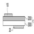
도 1은 본 발명의 제1 실시예의 제1 구현예에 따른 편광판 일체형 터치 감지 전극의 개략적인 평면도이다.
도 2는 본 발명의 제1 실시예의 제1 구현예 따른 편광판 일체형 터치 감지 전극의 개략적인 수직 단면도이다.
도 3은 본 발명의 제1 실시예의 제2 구현예로서, 복합 편광판의 편광판이 편광자와 보호필름의 적층체로 형성된 예의 개략적인 수직 단면도이다.
도 4는 본 발명의 제1 실시예의 제3 구현예로서, 복합 편광판의 편광판이 편광자와 보호필름의 적층체로 형성되고 적층순서가 도 3과 다른 예의 개략적인 수직 단면도이다.
도 5는 본 발명의 제1 실시예의 제4 구현예로서, 복합 편광판의 리타더가 경화 액정층과 기재의 적층체로 형성된 예의 개략적인 수직 단면도이다.
도 6은 본 발명의 제1 실시예의 제5 구현예로서, 복합 편광판의 리타더가 경화 액정층과 기재의 적층체로 형성되고 적층순서가 도 5와 다른 예의 개략적인 수직 단면도이다.
도 7은 본 발명의 제2 실시예의 제1 구현예로서, 복합 편광판의 편광판과 리타더의 적층 순서가 제1 실시예와 다른 예의 개략적인 수직 단면도이다.
도 8은 본 발명의 제3 실시예의 제1 구현예로서, 제1 감지 패턴과 제2 감지 패턴이 각각 복합 편광판의 서로 다른 면에 형성된 예의 개략적인 수직 단면도이다.
도 9는 본 발명의 제3 실시예의 제1 구현예에 따른 편광판 일체형 터치 감지 전극의 개략적인 평면도이다.
도 10은 본 발명의 제3 실시예의 제2 구현예로서, 복합 편광판의 리타더가 경화 액정층과 기재의 적층체로 형성된 예의 개략적인 수직 단면도이다.1 is a schematic plan view of a polarizing plate-integrated touch sensing electrode according to a first embodiment of the first embodiment of the present invention.
2 is a schematic vertical sectional view of a polarizing plate-integrated touch sensing electrode according to a first embodiment of the first embodiment of the present invention.
3 is a schematic vertical cross-sectional view of an example in which a polarizing plate of a composite polarizing plate is formed as a laminate of a polarizer and a protective film, according to a second embodiment of the first embodiment of the present invention.
4 is a schematic vertical cross-sectional view of a third embodiment of the first embodiment of the present invention, in which the polarizing plate of the composite polarizing plate is formed of a laminate of the polarizer and the protective film and the stacking order is different from that of FIG.
5 is a schematic vertical cross-sectional view of an example of a fourth embodiment of the first embodiment of the present invention in which the retarder of the composite polarizing plate is formed as a laminate of a cured liquid crystal layer and a substrate.
6 is a schematic vertical cross-sectional view of a fifth embodiment of the first embodiment of the present invention, in which the retarder of the composite polarizing plate is formed of a laminate of a cured liquid crystal layer and a substrate and the stacking order is different from that of Fig.
FIG. 7 is a schematic vertical cross-sectional view of an example in which the stacking order of the polarizer and the retarder of the composite polarizing plate is different from that of the first embodiment, according to the second embodiment of the present invention.
8 is a schematic vertical cross-sectional view of an example in which a first sensing pattern and a second sensing pattern are formed on different surfaces of a composite polarizing plate, respectively, according to a first embodiment of the third embodiment of the present invention.
9 is a schematic plan view of a polarizing plate-integrated touch sensing electrode according to a first embodiment of the third embodiment of the present invention.
10 is a schematic vertical cross-sectional view of an example of a second embodiment of the third embodiment of the present invention in which the retarder of the composite polarizing plate is formed as a laminate of a cured liquid crystal layer and a substrate.
본 발명은 리타더와 편광판이 코팅 방식으로 접합된 복합 편광판의 적어도 일면에 적어도 하나의 감지 패턴을 구비함으로써, 박막 구조를 구현할 수 있는, 복합 편광판 일체형 터치 감지 전극 및 이를 구비하는 터치 스크린 패널에 관한 것이다.
The present invention relates to a composite polarizer-integrated touch sensing electrode and a touch screen panel having the composite polarizer integrated touch sensor capable of realizing a thin film structure by providing at least one sensing pattern on at least one surface of a composite polarizer plate in which a retarder and a polarizer plate are bonded in a coating manner will be.
본 발명에 있어서, 복합 편광판이란 리타더와 편광판이 코팅 방식으로 접합되어 일체화된 광학 기능성 적층체를 의미한다. 구체적인 양태는 편광판이 리타더에 코팅되거나 리타더가 편광판에 코팅되는 구조이다. 이 때 코팅의 기판이 되는 리타더나 편광판 역시 다른 기판 또는 광학 필름에 도포된 코팅층일 수도 있다.In the present invention, the composite polarizing plate refers to an optical functional laminate in which a retarder and a polarizing plate are joined together in a coating manner to form an integral body. A specific embodiment is a structure in which the polarizer is coated on the retarder or the retarder is coated on the polarizer. At this time, the retarder or the polarizing plate which is a substrate of the coating may be a coating layer applied to another substrate or an optical film.
본 발명에 있어서, 편광판은 편광자 단일층 또는 편광자의 적어도 일면에 투명 보호 필름이 접합된 적층체일 수 있다. 따라서, 이하 본 발명에서 설명하는 편광판은 편광자 단일층 또는 편광자의 적어도 일면에 투명 보호 필름이 접합된 적층체로 이해되어야 한다.In the present invention, the polarizing plate may be a laminate in which a transparent protective film is bonded to at least one surface of a polarizer single layer or a polarizer. Accordingly, the polarizing plate described in the present invention should be understood as a laminate in which a transparent protective film is bonded to at least one surface of a polarizer single layer or a polarizer.
본 발명에 있어서, 리타더는 투과하는 광의 위상을 변경하는 기능을 한다. 예를 들면, 시야각 확대를 위한 광학 보상층 또는 반사 방지를 위한 4분파장판(1/4λ plate)일 수 있다. 본 발명의 복합 편광판 일체형 터치 감지 전극이 플렉서블 디스플레이에 사용되는 경우에는 4분파장판인 것이 바람직하다.In the present invention, the retarder functions to change the phase of transmitted light. For example, it may be an optical compensation layer for magnifying a viewing angle or a quarter-wave plate (1/4? Plate) for preventing reflection. When the complex-polarized-plate-integrated touch sensing electrode of the present invention is used in a flexible display, it is preferable that the polarizing plate is a quarter-wave plate.
본 발명에 있어서, 리타더는 단일층 또는 기재의 일면에 경화 액정막이 접합된 접합된 적층체일 수 있다. 따라서, 이하 본 발명에서 설명하는 리타더는 단일층 또는 기재의 일면에 경화 액정막이 접합된 적층체로 이해되어야 한다.
In the present invention, the retarder may be a single layer or a bonded laminate in which a hardened liquid crystal film is bonded to one surface of a substrate. Therefore, the retarder described in the present invention should be understood as a single layer or a laminate in which a hardened liquid crystal film is bonded to one surface of a substrate.
이하에서는 도면을 참조하여 본 발명을 보다 상세하게 설명하도록 한다. 다만, 본 명세서에 첨부되는 다음의 도면들은 본 발명의 바람직한 실시예를 예시하는 것이며, 전술한 발명의 내용과 함께 본 발명의 기술사상을 더욱 이해시키는 역할을 하는 것이므로, 본 발명은 그러한 도면에 기재된 사항에만 한정되어 해석되어서는 아니된다.
Hereinafter, the present invention will be described in detail with reference to the drawings. It is to be understood that both the foregoing general description and the following detailed description of the present invention are exemplary and explanatory and are intended to provide further explanation of the invention as claimed. And shall not be construed as limited to such matters.
제11st실시예Example
도 1 및 도 2에는 본 발명의 복합 편광판 일체형 터치 감지 전극의 일 실시예가 개략적으로 도시되어 있다. 도 1 및 도 2에 도시된 본 발명의 복합 편광판 일체형 터치 감지 전극은 복합 편광판의 일면에 제1 감지 패턴과 제2 감지 패턴이 모두 형성된 경우로서, 복합 편광판(1), 제1 감지 패턴(10), 제2 감지 패턴(20), 절연층(30) 및 브릿지 전극(50)을 구비한다.FIGS. 1 and 2 schematically show an embodiment of a touch sensing electrode integrated with a composite polarizer of the present invention. 1 and 2, the composite polarizer-integrated touch sensing electrode includes a
본 발명에 있어서, 터치 감지 전극을 형성하기 위한 별도의 기판을 사용하지 않고 복합 편광판에 직접 터치 감지 전극을 형성함으로써, 박막 구조를 달성할 수 있다.In the present invention, the thin film structure can be achieved by forming the touch sensing electrode directly on the complex polarizer without using a separate substrate for forming the touch sensing electrode.
터치 감지 전극은 x좌표를 감지하는 전극 패턴과 y좌표를 감지하는 전극 패턴의 2종류의 감지 패턴을 포함한다. 2종류의 감지 패턴은 각각 서로 다른 방향으로 형성된다. 제1 감지 패턴(10)과 제2 감지 패턴(20)은 서로 다른 방향으로 배치되어, 터치되는 지점의 X 좌표 및 Y 좌표에 대한 정보를 제공하게 된다. 구체적으로는, 사람의 손 또는 물체가 투명 기판에 접촉되면, 제1 감지 패턴(10), 제2 감지 패턴(20) 및 위치 검출라인을 경유하여 구동회로 측으로 접촉위치에 따른 정전용량의 변화가 전달된다. 그리고, X 및 Y 입력처리회로(미도시) 등에 의해 정전용량의 변화가 전기적 신호로 변환됨에 의해 접촉위치가 파악된다.The touch sensing electrode includes two types of sensing patterns: an electrode pattern for sensing the x coordinate and an electrode pattern for sensing the y coordinate. The two kinds of detection patterns are formed in different directions. The
이와 관련하여, 제1 감지 패턴(10) 및 제2 감지 패턴(20)은 복합 편광판(1)의 같은 일면 상에 형성되며, 터치되는 지점을 감지하기 위해서는 각 패턴들은 전기적으로 연결되어야 한다. 그런데, 제2 감지 패턴(20)은 서로 연결된 형태이지만 제1 감지 패턴(10)은 섬(island) 형태로 분리된 구조로 되어 있으므로 제1 감지 패턴(10)을 전기적으로 연결하기 위해서는 별도의 연결 전극(브릿지 전극)(50)이 필요하다.In this regard, the
하지만, 상기 브릿지 전극(50)은 제2 감지 패턴(20)과 전기적으로 연결되어서는 안되므로, 제2 감지 패턴(20)과는 다른 층에 형성되어야 한다. 이러한 구조를 나타내기 위해, 도 1의 A-A' 단면 중 브릿지 전극(50)이 형성된 부분의 확대도를 도 2에 도시하였다.However, since the
도 2를 참고하면, 복합 편광판(1) 상에 형성된 제1 감지 패턴(10)과 제2 감지 패턴(20)은 그 위에 형성된 절연막(30)으로 서로 전기적으로 절연되어 있는 상태이다. 그리고, 전술한 바와 같이 제1 감지 패턴(10)은 전기적으로 연결될 필요가 있으므로, 브릿지 전극(50)을 사용하여 전기적으로 연결된다.Referring to FIG. 2, the
섬 형태로 분리된 제1 감지 패턴(10)을 제2 감지 패턴(20)과는 전기적으로 차단되면서도 브릿지 전극(50)으로 연결하기 위해서는, 절연층(30) 상에 콘택홀(40)을 형성한 후에, 별도의 브릿지 전극(50)을 형성하는 단계를 거치게 된다.In order to connect the
본 발명에 있어서, 복합 편광판에 형성되는 터치 감지 전극의 제1 감지 패턴(10) 및 제2 감지 패턴(20)은 당분야에서 사용되는 재료가 제한 없이 사용될 수 있으며, 스크린에 표시되는 영상의 시인성을 저해하지 않기 위해서는, 투명 소재를 사용하거나 또는 미세 패턴으로 형성되는 것이 바람직하다. 구체적인 예를 들면, 인듐주석산화물(ITO), 인듐아연산화물(IZO), 아연산화물(ZnO), 인듐아연주석산화물(IZTO), 카드뮴주석산화물(CTO), PEDOT(poly(3,4-ethylenedioxythiophene)), 탄소나노튜브(CNT), 금속와이어 등을 들 수 있다. 이들은 단독 또는 2종 이상 혼합하여 사용할 수 있다.In the present invention, the
금속와이어에 사용되는 금속은 특별히 한정되지 않으며, 예를 들면 은(Ag), 금, 알루미늄, 구리, 철, 니켈, 티타늄, 텔레늄, 크롬 등을 들 수 있다. 이들은 단독 또는 2종 이상 혼합하여 사용할 수 있다.The metal used for the metal wire is not particularly limited, and examples thereof include silver (Ag), gold, aluminum, copper, iron, nickel, titanium, tellurium, chromium and the like. These may be used alone or in combination of two or more.
복합 편광판(1)의 편광자, 편광자 보호 필름, 기재, 경화 액정층 등의 광학 기능층 상에 감지 패턴(10, 20)을 형성하기 위해서는 광학 기능층 소재를 내열성이 우수한 것으로 사용하거나, 감지 패턴(10, 20)을 인쇄 방식, 코팅 방식, 저온(상온) 스퍼터링 등의 저온 공정을 적용하여 형성할 수도 있다.
In order to form the
또한, 본 발명은 종래 별도의 필름으로 구비되어 별도의 접착제를 사용하여 접착되던 편광판과 리타더를 복합 편광판으로 일체화함으로써 박막 구조를 달성하였다.In addition, the present invention achieves a thin film structure by integrating a polarizer and a retarder, which have been conventionally provided as separate films and are adhered using a separate adhesive, into a composite polarizer.
도 2에는 편광판(200)과 리타더(300)가 각각 단일층으로 형성된 제1 실시예의 제1 구현예가 도시되어 있다.FIG. 2 shows a first embodiment of the first embodiment in which the
단일층 편광판은 편광자 필름 또는 편광자 코팅층으로 형성될 수 있다.The single layer polarizing plate may be formed of a polarizer film or a polarizer coating layer.
먼저 편광자 필름으로는 당분야에서 사용되는 편광자가 특별한 제한 없이 사용될 수 있으며, 예를 들어, 편광자로 폴리비닐알콜계 수지로 된 필름에 이색성 염료가 흡착 배향된 것을 사용할 수 있다. 편광자를 구성하는 폴리비닐알콜계 수지로는 아세트산 비닐의 단독 중합체인 폴리아세트산비닐과, 아세트산 비닐과 이와 공중합 가능한 다른 단량체와의 공중합체등을 사용할 수 있다. 여기서 아세트산 비닐과 공중합 가능한 다른 단량체로는 불포화 카르복시산류, 불포화 술폰산류, 올레핀류, 비닐에테르류 및 암모늄기를 갖는 아크릴아미드류 등을 사용할 수 있다. 편광자의 두께는 특별히 제한되지 않으며, 당 분야에서 사용되는 통상적인 두께로 제조할 수 있다.As the polarizer film, a polarizer used in the art can be used without any particular limitation. For example, a polarizer can be used in which a dichroic dye is adsorbed and oriented on a film made of a polyvinyl alcohol resin. As the polyvinyl alcohol resin constituting the polarizer, a copolymer of polyvinyl acetate, which is a homopolymer of vinyl acetate, and vinyl acetate and other monomer copolymerizable therewith, may be used. Examples of other monomers copolymerizable with vinyl acetate include unsaturated carboxylic acids, unsaturated sulfonic acids, olefins, vinyl ethers, and acrylamides having an ammonium group. The thickness of the polarizer is not particularly limited, and can be made to be a conventional thickness used in the art.
또한, 편광자 코팅층으로는 고분자 수지 및 이색성 물질을 함유하는 고분자 용액을 코팅하여 형성될 수 있다. 코팅층 편광자는 편광판을 편광자 단일층으로 형성하는 경우에 바람직하게 사용될 수 있다.The polarizer coating layer may be formed by coating a polymer solution containing a polymer resin and a dichroic material. The coating layer polarizer can be preferably used when the polarizing plate is formed of a single polarizer layer.
편광자 코팅층을 형성하기 위한 고분자 수지로는 예를 들면 대표적으로 폴리비닐알코올계 수지가 사용될 수 있다. 폴리비닐알코올계 수지는 바람직하게는, 폴리아세트산 비닐계 수지를 비누화하여 얻은 폴리비닐알코올계 수지일 수 있다. 폴리아세트산 비닐계 수지로는 아세트산 비닐의 단독 중합체인 폴리아세트산 비닐 이외에, 아세트산 비닐과 이와 공중합 가능한 다른 단량체와의 공중합체 등을 들 수 있다. 아세트산 비닐과 공중합 가능한 다른 단량체로는 불포화 카르복시산계, 불포화 술폰산계, 올레핀계, 비닐에테르계, 암모늄기를 갖는 아크릴아미드계 단량체 등을 들 수 있다.As the polymer resin for forming the polarizer coating layer, for example, a polyvinyl alcohol-based resin may be typically used. The polyvinyl alcohol-based resin is preferably a polyvinyl alcohol-based resin obtained by saponifying a polyvinyl acetate-based resin. Examples of the polyvinyl acetate resin include polyvinyl acetate, which is a homopolymer of vinyl acetate, and copolymers of vinyl acetate and other monomers copolymerizable therewith. Other monomers copolymerizable with vinyl acetate include acrylamide monomers having an unsaturated carboxylic acid type, an unsaturated sulfonic acid type, an olefin type, a vinyl ether type, and an ammonium group.
또한 폴리비닐알코올계 수지는 변성된 것일 수도 있으며, 예를 들면 알데히드류로 변성된 폴리비닐포르말이나 폴리비닐아세탈일 수도 있다.The polyvinyl alcohol-based resin may be modified or may be polyvinyl formal or polyvinyl acetal modified with, for example, aldehydes.
이러한 폴리비닐알코올계 수지에 이색성 물질을 혼합하고 막을 형성함으로써 편광자층을 형성할 수 있다.A polarizer layer can be formed by mixing a dichroic material with such a polyvinyl alcohol-based resin and forming a film.
단일층 리타더 역시 리타더 필름 또는 리타더 코팅층으로 형성될 수 있다. 리타더 필름으로는 당분야에 사용되는 것이 특별한 제한 없이 사용될 수 있으며, 예를 들면 연신된 고분자 필름일 수 있다. 또한 리타더 코팅층은 반응성 액정 단량체를 함유하는 고분자 용액을 코팅하여 얻어질 수 있다.The single layer retarder may also be formed with a retarder film or a retarder coating layer. As the retarder film, those used in the art can be used without any particular limitation, for example, a stretched polymer film. Further, the retarder coating layer can be obtained by coating a polymer solution containing a reactive liquid crystal monomer.
편광판(200)과 리타더(300)가 모두 단일층으로 형성되는 경우에는 가장 얇은 박막 구조를 형성할 수 있는 장점이 있다.When both the
본 발명의 제1 실시예의 제2 구현예로서, 편광판(200)은 편광자(210)와 보호 필름(220)의 적층체일 수 있다. 도 3에는 제1 실시예의 제2 구현예가 개략적으로 도시되어 있다.As a second embodiment of the first embodiment of the present invention, the
본 발명에서 사용 가능한 보호 필름(220)으로는 투명성, 기계적 강도, 열안정성, 수분차폐성, 등방성 등에서 우수한 필름이 사용될 수 있다. 구체적인 예로는, 폴리에틸렌테레프탈레이트, 폴리에틸렌이소프탈레이트, 폴리에틸렌나프탈레이트, 폴리부틸렌테레프탈레이트 등의 폴리에스테르계 수지; 디아세틸셀룰로오스, 트리아세틸셀룰로오스 등의 셀룰로오스계 수지; 폴리카보네이트계 수지; 폴리메틸(메타)아크릴레이트, 폴리에틸(메타)아크릴레이트 등의 아크릴계 수지; 폴리스티렌, 아크릴로니트릴-스티렌 공중합체 등의 스티렌계 수지; 폴리에틸렌, 폴리프로필렌, 시클로계 또는 노보넨 구조를 갖는 폴리올레핀, 에틸렌-프로필렌 공중합체 등의 폴리올레핀계 수지; 염화비닐계 수지; 나일론, 방향족 폴리아미드 등의 아미드계 수지; 이미드계 수지; 폴리에테르술폰계 수지; 술폰계 수지; 폴리에테르에테르케톤계 수지; 황화 폴리페닐렌계 수지; 비닐알코올계 수지; 염화비닐리덴계 수지; 비닐부티랄계 수지; 알릴레이트계 수지; 폴리옥시메틸렌계 수지; 에폭시계 수지 등과 같은 열가소성 수지로 구성된 필름을 들 수 있으며, 상기 열가소성 수지의 블렌드물로 구성된 필름도 사용할 수 있다. 또한, (메타)아크릴계, 우레탄계, 아크릴우레탄계, 에폭시계, 실리콘계 등의 열경화성 수지 또는 자외선 경화형 수지로 된 필름을 이용할 수도 있다.As the
편광자 보호 필름 중의 상기 열가소성 수지의 함량은 50 내지 100중량%, 바람직하게는 50 내지 99중량%, 보다 바람직하게는 60 내지 98중량%, 가장 바람직하게는 70 내지 97중량%인 것이 좋다. 그 함량이 50중량% 미만인 경우에는 열가소성 수지가 가지고 있는 본래의 고투명성을 충분히 발현하지 못할 수 있다.The content of the thermoplastic resin in the polarizer protective film is preferably 50 to 100% by weight, preferably 50 to 99% by weight, more preferably 60 to 98% by weight, and most preferably 70 to 97% by weight. When the content is less than 50% by weight, the inherent high transparency of the thermoplastic resin may not be sufficiently exhibited.
이러한 투명 보호 필름은 적절한 1종 이상의 첨가제가 함유된 것일 수도 있다. 첨가제로는, 예컨대 자외선흡수제, 산화방지제, 윤활제, 가소제, 이형제, 착색방지제, 난연제, 핵제, 대전방지제, 안료, 착색제 등을 들 수 있다.Such a transparent protective film may contain one or more suitable additives. Examples of the additive include an ultraviolet absorber, an antioxidant, a lubricant, a plasticizer, a release agent, a coloring inhibitor, a flame retardant, a nucleating agent, an antistatic agent, a pigment and a colorant.
또한, 필요에 따라 보호 필름은 표면 처리된 것일 수 있다. 이러한 표면 처리로는 플라즈마 처리, 코로나 처리, 프라이머 처리 등의 건식 처리, 검화 처리를 포함하는 알칼리 처리 등의 화학 처리 등을 들 수 있다.Further, if necessary, the protective film may be surface-treated. Examples of the surface treatment include a chemical treatment such as an alkaline treatment including a dry treatment such as a plasma treatment, a corona treatment, a primer treatment, and a saponification treatment.
본 구현예에서, 리타더(300)는 편광판의 보호 필름(220)에 코팅되어 형성될 수 있다. 또한, 편광자(210)는 편광자 필름이거나 편광자 코팅층일 수 있다.In this embodiment, the
본 구현예는 편광판의 보호 필름(220)이 편광자(210)를 지지할 뿐만 아니라 리타더(300)의 기재 역할도 담당하고, 복합 편광판(1)의 강성을 유지하는 기능을 담당하게 된다.The
도 4에는 제1 실시예의 제3 구현예로서, 도 3과는 편광자(210)과 보호 필름(220)의 적층 순서가 반대인 예시가 개략적으로 도시되어 있다. 본 구현예에서는 터치 감지 전극이 보호 필름(220) 상에 형성되고, 리타더(300)는 편광자(210)에 직접 접합된다.FIG. 4 schematically shows an example in which the stacking order of the
본 구현예에서는, 터치 감지 전극이 보호 필름(220) 상에 형성되므로 보다 안정적으로 형성될 수 있는 장점이 있다.In this embodiment, since the touch sensing electrode is formed on the
본 발명의 제1 실시예의 제4 구현예로서, 리타더(300)는 기재(320)와 경화 액정막(310)의 적층체일 수 있다. 도 5에는 제1 실시예의 제4 구현예가 개략적으로 도시되어 있다.As a fourth embodiment of the first embodiment of the present invention, the
본 발명에 있어서 기재(320)는 통상적인 보호 필름일 수도 있고, 액정성 화합물의 배향을 유도하는 배향막일 수도 있으며, 둘 다의 적층막일 수도 있다.In the present invention, the
기재(320)로서 사용되는 보호 필름은 전술한 편광자의 보호 필름에서 사용된 필름이 동일한 범주 내에서 사용될 수 있으며, 배향막은 당분야에서 사용되는 배향막이 특별한 제한 없이 적용될 수 있다.The protective film used as the
본 구현예에서는, 편광판(200)이 리타더의 경화 액정층(310)에 직접 코팅되어 형성된다.
In this embodiment, the
도 6에는 제1 실시예의 제5 구현예로서, 도 5와는 기재(320)와 경화 액정막(310)의 적층 순서가 반대인 예시가 개략적으로 도시되어 있다. 본 구현예에서는 편광판(200)이 리타더의 기재(320)에 코팅되어 형성된다.Fig. 6 schematically shows an example in which the order of stacking of the
본 구현예는 리타더의 기재(320)가 경화 액정막(310)을 지지할 뿐만 아니라 코팅되는 편광판(200)의 기재 역할도 담당하고, 복합 편광판(1)의 강성을 유지하는 기능을 담당하게 된다.
This embodiment is characterized in that the
제2Second실시예Example
도 7에는 본 발명의 제2 실시예의 제1 구현예가 개략적으로 도시되어 있다.Fig. 7 schematically shows a first embodiment of the second embodiment of the present invention.
제2 실시예의 제1 구현예는 제1 실시예의 제1 구현예와는 적층 순서가 다른 것을 제외하고는 동일한 구조를 갖는다.The first embodiment of the second embodiment has the same structure except that the stacking order is different from that of the first embodiment of the first embodiment.
또한, 본 발명의 제2 실시예는 편광판(200) 및 리타더(300)의 구체적인 구조에 대해서 제1 실시예의 제2 구현예 내지 제5 구현예와 동일한 적층구조의 구현예를 가질 수 있으며, 구체적인 설명은 제1 실시예서 설명한 것으로 갈음하도록 한다.
In addition, the second embodiment of the present invention may have the same laminated structure as the second to fifth embodiments of the first embodiment with respect to the specific structure of the
제3Third실시예Example
도 8에는 본 발명의 제3 실시예의 제1 구현예가 개략적으로 도시되어 있다.FIG. 8 schematically shows a first embodiment of the third embodiment of the present invention.
도 8을 참고하면, 본 발명의 복합 편광판 일체형 터치 감지 전극은 제1 감지 패턴(10)과 제2 감지 패턴(20)이 복합 편광판(1)의 서로 다른 일면에 각각 형성된 구조를 갖는다. 이와 같이 제1 감지 패턴(10)과 제2 감지 패턴(20)이 복합 편광판(1)의 서로 다른 면에 형성되면, 복합 편광판(1)이 제1 감지 패턴(10)과 제2 감지 패턴(20) 간의 전기적 절연을 달성하게 되어 별도의 절연층을 구비할 필요가 없으므로, 박막 구조의 구현이 가능하다.Referring to FIG. 8, the compound sensing polarity integrated type touch sensing electrode of the present invention has a structure in which the
또한, 도 8의 복합 편광판 일체형 터치 감지 전극의 개략적인 평면도가 도 9에 도시되어 있다. 도 9를 참고하면, 제1 감지 패턴(10)과 제2 감지 패턴(20)이 동일한 평면 상에 형성되는 경우에는 도 1 및 도 2에 도시된 바와 같이 브릿지 전극(50)이 필요하나, 본 실시예에서는 서로 다른 감지 패턴이 다른 평면 상에 위치하게 되므로 각 패턴은 브릿지 전극(50) 필요 없이 전기적으로 연결된 구조를 가질 수 있다. 따라서 박막 구조의 구현뿐만 아니라 터치 감지 전극의 제조 공정도 현저하게 단축시킬 수 있다.A schematic plan view of the composite-polarized-plate integrated type touch sensing electrode of Fig. 8 is shown in Fig. Referring to FIG. 9, when the
본 구현예에서는 편광판(200)과 리타더(300)가 모두 단일층으로 형성된 구조를 가지며, 편광판(200)과 리타더(300)에 관련된 사항은 제1 실시예에서 설명한 것과 동일하게 적용이 가능하다.In this embodiment, both the
또한, 본 발명의 제3 실시예는 편광판(200) 및 리타더(300)의 구체적인 구조에 대해서 제1 실시예의 제2 구현예 내지 제5 구현예와 동일한 적층구조의 구현예를 가질 수 있으며, 구체적인 설명은 제1 실시예서 설명한 것으로 갈음하도록 한다. 참고로, 도 10에는 제3 실시예의 제2 구현예로서, 리타더(300)가 기재(320)와 경화 액정막(310)의 적층체인 예시가 개략적으로 도시되어 있다. 제3 실시예의 제2 구현예의 구체적인 설명에 대해서는 이에 대응하는 제1 실시예의 제5 구현예에서의 설명으로 갈음할 수 있다.
In addition, the third embodiment of the present invention may have the same laminated structure as the second to fifth embodiments of the first embodiment with respect to the specific structure of the
굴절률Refractive index
본 발명의 복합 편광판 일체형 터치 감지 전극은 복합 편광판과 감지 전극의 굴절률 차이를 조절함으로써, 시인성을 더욱 개선할 수 있다.INDUSTRIAL APPLICABILITY The touch sensing electrode with integrated polarizing plate of the present invention can further improve the visibility by controlling the refractive index difference between the composite polarizing plate and the sensing electrode.
예를 들면, 복합 편광판과 복합 편광판의 일면에 구비된 감지 패턴의 굴절률의 차이는 0.8 이하일 수 있다. 감지 패턴은 반사율이 높아 주변과 반사율 차이가 크게 되면 육안으로 식별되어, 시인성이 저하될 수 있다. 이에 본 발명은 복합 편광판과 복합 편광판에 구비되는 감지 패턴의 굴절률 차이를 0.8이하로 하여 감지 패턴과 복합 편광판의 반사율 차이를 최소화함으로써, 시인성을 보다 개선할 수 있다. 복합 편광판과 감지 패턴의 구체적인 굴절률 값은 각 층의 두께, 구체적인 소재의 종류 등 당분야에 공지된 방법으로 조절될 수 있다. 이러한 측면에서, 감지 패턴의 굴절률은 1.3 내지 2.5인 것이 바람직하다. 감지 패턴의 굴절률이 상기 범위인 경우 복합 편광판과의 굴절률 차이가 본 발명 범위에 포함되기가 용이하고 시인성 개선 효과가 보다 뛰어나다.
For example, the refractive index difference of the detection patterns provided on one surface of the composite polarizing plate and the composite polarizing plate may be 0.8 or less. Since the detection pattern has a high reflectance, if the difference between the periphery and the reflectance is large, it is visually recognized and visibility may be deteriorated. Accordingly, the present invention minimizes the reflectance difference between the sensing pattern and the composite polarizer by setting the refractive index difference of the sensing pattern provided in the complex polarizer and the composite polarizer to 0.8 or less, thereby further improving the visibility. The specific refractive index values of the composite polarizing plate and the detection pattern can be adjusted by methods known in the art such as the thickness of each layer and the specific material type. In this respect, the refractive index of the detection pattern is preferably 1.3 to 2.5. When the refractive index of the detection pattern is within the above range, the refractive index difference with the complex polarizing plate is easily included in the scope of the present invention, and the effect of improving visibility is more excellent.
전술한 바와 같은 본 발명의 복합 편광판 일체형 터치 감지 전극은 추후 운송 및 타 부품과의 접합에 용이하도록 적어도 일면에 점착층 및 이형필름이 순차적으로 적층된 구조를 더 구비할 수도 있다.The composite polarizing plate integrated type touch sensing electrode of the present invention as described above may further include a structure in which an adhesive layer and a release film are sequentially laminated on at least one surface to facilitate subsequent transportation and bonding with other components.
본 발명의 복합 편광판 일체형 터치 감지 전극은 당분야에 공지된 추가 공정을 통해 터치 스크린 패널을 형성할 수 있다.The composite polarizer-integrated touch sensing electrode of the present invention can form a touch screen panel through an additional process known in the art.
예를 들면, 본 발명의 복합 편광판 일체형 터치 감지 전극은 그 상부 및 하부에 각각 광학 기능성 필름이 점접착체로 접합될 수 있다. 본 발명에 있어서, 점접착제란 점착제 또는 접착제를 의미한다. 또한, 본 발명에 있어서 복합 편광판의 상부란 복합 편광판을 기준으로 시인측을 의미하며, 복합 편광판의 하부란 복합 편광판을 기준으로 시인측의 반대편을 의미한다.For example, the composite polarizing plate integrated type touch sensing electrode of the present invention can be bonded to the upper and lower portions of the touch sensing electrode with a point-stick material, respectively. In the present invention, the point adhesive means a pressure sensitive adhesive or an adhesive. In addition, in the present invention, the upper part of the complex polarizer refers to the viewing side relative to the composite polarizer, and the lower part of the composite polarizer refers to the opposite side of the composite polarizer from the viewer side.
이 경우 복합 편광판의 상면에 적어도 하나의 감지 패턴이 구비되면, 상부에 배치된 점접착제층의 굴절률과 상기 상면의 감지 패턴의 굴절률 차이는 0.3 이하인 것이 감지 패턴의 시인성 개선 측면에서 바람직하다. 입사된 광이 복합 편광판을 통과하기 전에 점접착제층과 감지 패턴에 입사되므로 점접착제층과 감지 패턴의 굴절률이 0.3 이하이어야 감지 패턴의 반사율을 낮출 수 있다.In this case, if at least one sensing pattern is provided on the upper surface of the composite polarizing plate, the difference between the refractive index of the upper adhesive layer and the refractive index of the sensing pattern on the upper surface is preferably 0.3 or less in view of improving the visibility of the sensing pattern. Since the incident light enters the point adhesive layer and the sensing pattern before passing through the complex polarizer, the refractive index of the point adhesive layer and the sensing pattern must be 0.3 or less so that the reflectance of the sensing pattern can be lowered.
복합 편광판이 상면과 하면에 각각 감지 패턴이 구비되게 되면(상면에 제1 감지 패턴 하면에 제2 감지 패턴), 상면의 감지 패턴은 전술한 바와 같이 상부의 점접착제층과 굴절률 차이가 0.3 이하이어야 하고, 하면의 감지 패턴은 상부의 점접착제층과 굴절률 차이가 0.8 이하인 것이 바람직하다. 하면의 감지 패턴은 상부의 점접착제층과 굴절률 차이가 0.8을 초과하게 되면 하면 감지 패턴의 시인성이 저하될 수 있다.When the composite polarizing plate is provided with the detection patterns on the upper surface and the lower surface (the first detection pattern on the upper surface and the second detection pattern on the lower surface), the difference in refractive index between the upper surface and the upper adhesive layer is 0.3 or less And the difference in refractive index between the lower surface of the adhesive layer and the upper adhesive layer is 0.8 or less. If the difference in refractive index between the bottom sensing pattern and the top adhesive layer exceeds 0.8, the visibility of the bottom sensing pattern may be degraded.
본 발명의 다른 구현예로서, 복합 편광판의 하면에 제1 감지 패턴 및 제2 감지 패턴을 모두 구비되고, 복합 편광판의 상면에 광학 기능성 필름이 점접착체로 접합되는 경우에는, 점접착제층의 굴절률과 상기 하면의 감지 패턴의 굴절률 차이는 0.8 이하인 것이 바람직하다. 전술한 바와 같이, 하면의 감지 패턴은 상부의 점접착제층과 굴절률 차이가 0.8를 초과하게 되면 하면 감지 패턴의 시인성이 저하될 수 있다.In another embodiment of the present invention, in a case where both the first sensing pattern and the second sensing pattern are provided on the lower surface of the composite polarizing plate and the optically functional film is bonded to the upper surface of the composite polarizing plate by a point-adhesive material, The refractive index difference of the detection pattern on the lower surface is preferably 0.8 or less. As described above, when the difference in refractive index between the upper and lower adhesive layers is greater than 0.8, the visibility of the lower sensing pattern may be lowered.
본 발명의 복합 편광판 일체형 터치 감지 전극에 접합될 수 있는 광학 기능성 필름으로는 예를 들면, 윈도우 커버 필름, 반사방지필름, 방오필름, 하드코팅필름 등이 있을 수 있으나, 이에 한정되는 것은 아니다.Examples of the optical functional film that can be bonded to the composite polarizing plate integrated type touch sensing electrode of the present invention include, but are not limited to, a window cover film, an antireflection film, an antifouling film, a hard coating film and the like.
이와 같은 본 발명에 따른 터치 스크린 패널은 액정 디스플레이, OLED, 플렉서블 디스플레이 등의 디스플레이 장치와 결합될 수 있다.
The touch screen panel according to the present invention can be combined with a display device such as a liquid crystal display, an OLED, and a flexible display.
제조Produce실시예Example
먼저 리타더 필름의 한면에 코팅형 편광자를 코팅하여, 투과율 42%의 편광판을 제조한 후, 편광자가 코팅된 리타더의 반대면에 ITO를 상온 증착 및 열처리하여 ITO층을 형성하였다. 이후 Photolithography 공정을 이용하여 상기 ITO층을 터치 패턴으로 제조하였다. 이후 상기 터치 패턴 상에 절연층을 제막하고 컨택홀을 형성한 후, 금속물질을 증착 및 에칭하여 배선 전극과 브릿지 전극을 형성하였으며, 상기 코팅형 편광자측에 윈도우 필름을 접합하여 터치 모듈을 제조하였다.
First, a coated polarizer was coated on one side of the retarder film to prepare a polarizer having a transmittance of 42%, and ITO was formed on the opposite side of the polarizer-coated retarder by normal temperature deposition and heat treatment to form an ITO layer. Then, the ITO layer was formed into a touch pattern using a photolithography process. Then, an insulation layer was formed on the touch pattern to form a contact hole. Then, a metal material was deposited and etched to form a wiring electrode and a bridge electrode, and a window film was bonded to the coated polarizer side to produce a touch module .
제조Produce비교예Comparative Example
PET 기재필름의 한면에 ITO를 상온 증착 및 열처리하여 ITO층을 형성하였다. 이후 Photolithography 공정을 이용하여 상기 ITO층을 터치 패턴으로 제조하고, 금속물질을 증착 및 에칭하여 배선 전극을 형성한 터치 전극 필름을 2매 제작하여 접합하는 방식으로 FF 방식의 터치 센서를 제작한 후, 윈도우 필름과 편광판 사이에 접합하고, 상기 편광판의 반대편에는 리타더를 접합하여 터치 모듈을 제작하였다.
ITO was deposited on the PET substrate film at room temperature and heat-treated to form an ITO layer. Thereafter, the ITO layer is formed into a touch pattern using a photolithography process, and two touch electrode films on which wiring electrodes are formed by depositing and etching a metal material are bonded to form a touch sensor of the FF type, The touch module was manufactured by bonding a window film and a polarizer, and bonding a retarder to the opposite side of the polarizer.
실험예Experimental Example
제조실시예 및 제조비교예에서 제조된 터치 모듈을 이용하여, 하기의 실험을 수행하였다.
The following experiment was conducted using the touch module manufactured in the production example and the comparative example.
A. Dynamic Bending TestA. Dynamic Bending Test
Bending Test 기기 (MIT)를 활용하여, R=3mm의 반경으로 좌우의 반복 굴곡 실험을 실시하였다. Sample의 폭은 10mm , 길이는 150mm 이며, 5만회까지의 반복 굴곡 실험 중 끊어지는 지점과 Film Layer 간의 박리를 파악하였다.
Bending test equipment (MIT) was used to perform left and right bending tests with a radius of R = 3 mm. The width of the sample was 10 mm and the length was 150 mm, and the separation between the breaking point and the film layer was observed during repeated bending experiments up to 50,000 times.
B. 두께 측정B. Thickness measurement
상기 방법에 의해서 제조된 터치 모듈의 총 두께를 마이크로 미터를 활용하여 측정하였다.
The total thickness of the touch module manufactured by the above method was measured using a micrometer.
(Layer 박리)Number of bends
(Layer exfoliation)
(Film 파단)Number of bends
(Film break)
실시예Example 1-10 1-10
하기 표 2에 기재된 굴절률로 복합편광판 일체형 터치 감지 전극을 제조하여, 패턴부와 비패턴부의 위치별 평균 반사율을 측정하였다. 패턴부는 감지 패턴이 형성된 부분이고, 비패턴부는 감지 패턴이 형성되지 않은 부분(즉, 절연층이나 리타더가 노출된 부분)이다.A touch sensing electrode with a composite polarizer integrated with a refractive index as shown in Table 2 below was prepared and the average reflectance of the pattern portion and the non-pattern portion was measured. The pattern portion is a portion where a sensing pattern is formed, and the non-pattern portion is a portion where a sensing pattern is not formed (i.e., an insulating layer or a portion where the retarder is exposed).
상기 평균반사율은 400nm~700nm에서의 반사율의 평균을 의미한다.The average reflectance means an average of reflectance at 400 nm to 700 nm.
(전극/기재)? Reflectance (%)
(Electrode / substrate)
1면materials
One side
1면materials
One side
1면materials
One side
1면materials
One side
1면materials
One side
1면materials
One side
1면materials
One side
1면materials
One side
1면materials
One side
1면materials
One side
2면materials
Two sides
1면materials
One side
2면materials
Two sides
1면materials
One side
2면materials
Two sides
1면materials
One side
1면materials
One side
1면materials
One side
1면materials
One side
1면materials
One side
1면materials
One side
1면materials
One side
2면materials
Two sides
1면materials
One side
2면materials
Two sides
a-1:폴리카보네이트 필름 리타더가 부착된 편광판
a-2:코팅층형 리타더가 부착된 편광판
제1 감지 패턴: ITO
제2 감지 패턴: ITO
절연층: 유기절연막
상기 굴절률과 소멸계수는 550nm 파장의 광을 기준으로 함.Complex polarizer
a-1: Polarizer with Polycarbonate Film Retarder
a-2: Polarizer with coating layer type retarder
First detection pattern: ITO
Second detection pattern: ITO
Insulating layer: organic insulating film
The refractive index and extinction coefficient are based on light having a wavelength of 550 nm.
상기 표 2를 참고하면, 복합 편광판과 감지 패턴의 굴절률 차이가 0.8 이하인 경우가 그렇지 않은 경우보다 시인성이 보다 우수한 것을 확인할 수 있다.
Referring to Table 2, it can be seen that the difference in refractive index between the composite polarizing plate and the sensing pattern is 0.8 or less, which is better than the case where the refractive index difference is 0.8 or less.
10: 제1 감지 패턴20: 제2 감지 패턴
30: 절연층
40: 콘택홀50: 브릿지 전극
200: 편광판
210: 편광자220: 편광자 보호 필름
300: 리타더
310: 경화 액정층320: 기재10: first detection pattern 20: second detection pattern
30: Insulation layer
40: contact hole 50: bridge electrode
200: polarizer
210: Polarizer 220: Polarizer protective film
300: retarder
310: cured liquid crystal layer 320: substrate
Claims (15)
Translated fromKorean상기 복합 편광판과 상기 복합 편광판의 일면에 구비된 감지 패턴의 굴절률의 차이가 0.8 이하인, 복합 편광판 일체형 터치 감지 전극.
At least one sensing pattern is provided on at least one surface of a composite polarizing plate in which a retarder and a polarizing plate are bonded in a coating manner,
Wherein the refractive index difference of the sensing patterns provided on one surface of the composite polarizing plate and the composite polarizing plate is 0.8 or less.
The touch sensing electrode as claimed in claim 1, wherein at least one of the retarder and the polarizing plate is a coating layer.
The touch sensing electrode as claimed in claim 2, wherein the polarizing plate other than the coating layer is a laminate in which a transparent protective film is bonded to at least one surface of the polarizer.
The touch sensing electrode as claimed in claim 2, wherein the non-coating layer is a laminate in which a hardened liquid crystal film is bonded to one surface of a substrate.
The touch sensing electrode of claim 1, wherein the first sensing pattern and the second sensing pattern are formed on only one side of the composite polarizer.
The touch sensing electrode of claim 1, wherein the first sensing pattern is formed on one surface of the complex polarizer, and the second sensing pattern is formed on the other surface of the complex polarizer.
The touch sensing electrode of claim 1, wherein the refractive index of the sensing pattern is 1.3 to 2.5.
[2] The method according to claim 1, wherein the composite polarizer comprises a first polarized light sensing element having a first sensing pattern and a second sensing pattern on one surface thereof, a bridge electrode electrically connecting the insulation layer and the first sensing pattern spaced on the insulation layer, And a second electrode formed on the first electrode.
[Claim 2] The method according to claim 1, wherein the composite polarizing plate has a first sensing pattern on one side and a second sensing pattern on the other side of the composite polarizing plate, and the composite polarizing plate has electrical insulation between the first sensing pattern and the second sensing pattern. Forming a composite polarizer integrated touch sensing electrode.
A touch screen panel comprising the composite polarizer-integrated touch sensing electrode of any one of claims 1 to 6 and 8 to 10.
[14] The method of claim 11, wherein the complex polarizer-integrated touch sensing electrode comprises at least one sensing pattern on an upper surface of the complex polarizer, and an optical functional film is bonded to the upper surface of the complex polarizer with a point- Wherein the refractive index difference of the pattern is 0.3 or less.
[Claim 13] The touch screen panel of claim 12, wherein a refractive index of the point adhesive is different from a refractive index of a sensing pattern of a bottom surface of the complex polarizer is 0.8 or less.
[14] The method of claim 11, wherein the composite polarizer-integrated touch sensing electrode has a first sensing pattern and a second sensing pattern on a lower surface of the composite polarizer, and the optical functional film is bonded to the upper surface of the composite polarizer with a point- Wherein the difference between the refractive index and the refractive index of the sensing pattern of the lower surface is 0.8 or less.
Priority Applications (6)
| Application Number | Priority Date | Filing Date | Title |
|---|---|---|---|
| KR1020130141669AKR101444132B1 (en) | 2013-11-20 | 2013-11-20 | Touch sensing electrode combined with complexed polarization plate and touch screen panel comprising the same |
| CN201480063814.8ACN105793805B (en) | 2013-11-20 | 2014-10-28 | Composite polarizing plate-integrates touch-control sensing electrode and the touch-screen panel including it |
| EP14863195.5AEP3073357B1 (en) | 2013-11-20 | 2014-10-28 | Composite polarizing plate-integrated touch sensing electrode and touch screen panel having same |
| US15/038,158US20160283025A1 (en) | 2013-11-20 | 2014-10-28 | Composite polarizing plate-integrated touch sensing electrode and touch screen panel having same |
| PCT/KR2014/010144WO2015076505A1 (en) | 2013-11-20 | 2014-10-28 | Composite polarizing plate-integrated touch sensing electrode and touch screen panel having same |
| TW103138172ATW201523386A (en) | 2013-11-20 | 2014-11-04 | Composite polarizing plate-integrated touch sensing electrode and touch screen panel including the same |
Applications Claiming Priority (1)
| Application Number | Priority Date | Filing Date | Title |
|---|---|---|---|
| KR1020130141669AKR101444132B1 (en) | 2013-11-20 | 2013-11-20 | Touch sensing electrode combined with complexed polarization plate and touch screen panel comprising the same |
Publications (1)
| Publication Number | Publication Date |
|---|---|
| KR101444132B1true KR101444132B1 (en) | 2014-11-04 |
Family
ID=52288961
Family Applications (1)
| Application Number | Title | Priority Date | Filing Date |
|---|---|---|---|
| KR1020130141669AActiveKR101444132B1 (en) | 2013-11-20 | 2013-11-20 | Touch sensing electrode combined with complexed polarization plate and touch screen panel comprising the same |
Country Status (6)
| Country | Link |
|---|---|
| US (1) | US20160283025A1 (en) |
| EP (1) | EP3073357B1 (en) |
| KR (1) | KR101444132B1 (en) |
| CN (1) | CN105793805B (en) |
| TW (1) | TW201523386A (en) |
| WO (1) | WO2015076505A1 (en) |
Cited By (5)
| Publication number | Priority date | Publication date | Assignee | Title |
|---|---|---|---|---|
| KR20160086486A (en)* | 2015-01-09 | 2016-07-20 | 삼성디스플레이 주식회사 | Touch panel and organic light emitting diode display |
| CN106055173A (en)* | 2015-04-17 | 2016-10-26 | 三星显示有限公司 | Touch panel |
| WO2018016811A1 (en)* | 2016-07-21 | 2018-01-25 | 동우화인켐 주식회사 | Film touch sensor |
| KR101858709B1 (en)* | 2016-08-05 | 2018-05-16 | 동우 화인켐 주식회사 | Touch sensor laminate, touch screen panel and display device comprising the same |
| EP3043247B1 (en)* | 2015-01-09 | 2021-03-24 | Samsung Display Co., Ltd. | Flexible touch panel and flexible display device |
Families Citing this family (12)
| Publication number | Priority date | Publication date | Assignee | Title |
|---|---|---|---|---|
| CN105094402B (en)* | 2014-05-15 | 2018-06-12 | 宸鸿科技(厦门)有限公司 | Touch control display device |
| CN104656993A (en)* | 2015-02-13 | 2015-05-27 | 业成光电(深圳)有限公司 | Film type touch panel structure |
| CN107636576B (en)* | 2015-05-08 | 2021-01-29 | 东友精细化工有限公司 | Touch sensor integrated with polarizer and organic light emitting display device |
| KR102008603B1 (en)* | 2015-05-29 | 2019-08-07 | 후지필름 가부시키가이샤 | Organic electro luminescence display |
| TWI568579B (en)* | 2015-11-02 | 2017-02-01 | 住華科技股份有限公司 | Polarizing plate |
| KR102446435B1 (en)* | 2015-12-29 | 2022-09-23 | 삼성디스플레이 주식회사 | Touch panel, manufacturing method thereof, and display device including same |
| KR102460003B1 (en) | 2016-01-08 | 2022-10-31 | 삼성디스플레이 주식회사 | λ/4 PHASE DIFFERENCE FILM, DISPLAY APPARATUS AND MANUFATURING METHOD THEREOF |
| CN106226856A (en)* | 2016-08-03 | 2016-12-14 | 京东方科技集团股份有限公司 | A kind of polaroid and display device |
| KR102158204B1 (en)* | 2017-08-24 | 2020-09-22 | 동우 화인켐 주식회사 | Film antenna and display device including the same |
| KR102494625B1 (en)* | 2017-08-28 | 2023-02-01 | 삼성디스플레이 주식회사 | Display device |
| CN109343742B (en)* | 2018-12-06 | 2024-03-26 | 苏州泛普科技股份有限公司 | High-precision mimicry touch module |
| KR102795209B1 (en)* | 2019-08-30 | 2025-04-14 | 엘지디스플레이 주식회사 | Touch display device |
Citations (3)
| Publication number | Priority date | Publication date | Assignee | Title |
|---|---|---|---|---|
| KR20120044041A (en)* | 2010-10-27 | 2012-05-07 | 삼성모바일디스플레이주식회사 | Display device |
| KR20120105984A (en)* | 2011-03-17 | 2012-09-26 | 엘지전자 주식회사 | Transparent electrode film structure and touch sreen |
| KR20130119658A (en)* | 2012-04-24 | 2013-11-01 | 삼성디스플레이 주식회사 | Flexible touch screen panel |
Family Cites Families (24)
| Publication number | Priority date | Publication date | Assignee | Title |
|---|---|---|---|---|
| JP4577734B2 (en)* | 1998-02-24 | 2010-11-10 | Dowaホールディングス株式会社 | Low reflective resistive touch panel and method for manufacturing the same |
| DE69932826T2 (en)* | 1998-06-18 | 2006-12-14 | Kaneka Corp. | TRANSPARENT TOUCH PANEL AND LIQUID CRYSTAL DISPLAY WITH A TRANSPARENT TOUCH PANEL |
| AU2001253613A1 (en)* | 2000-04-17 | 2001-10-30 | Circadence Corporation | System and method for shifting functionality between multiple web servers |
| JP2002148592A (en)* | 2000-08-31 | 2002-05-22 | Sumitomo Chem Co Ltd | Liquid crystal display |
| TWI281057B (en)* | 2004-08-10 | 2007-05-11 | Optimax Tech Corp | A thin brightness enhancement polarizer |
| EP1892609A4 (en)* | 2005-05-26 | 2013-03-27 | Gunze Kk | Transparent planar body and transparent touch switch |
| KR20080073252A (en) | 2007-02-05 | 2008-08-08 | (주)유비카드 | Flexible liquid crystal display |
| CN101617249B (en)* | 2007-08-14 | 2014-07-09 | Lg化学株式会社 | Optical film and method for producing same |
| KR101065313B1 (en)* | 2008-11-14 | 2011-09-16 | 삼성모바일디스플레이주식회사 | Organic light emitting display device |
| JP5484891B2 (en)* | 2009-03-04 | 2014-05-07 | 株式会社ジャパンディスプレイ | Display device |
| TWI379226B (en)* | 2009-03-13 | 2012-12-11 | Tpk Touch Solutions Inc | Liquid crystal display with integrated capacitive touch device |
| TWI424197B (en)* | 2010-06-23 | 2014-01-21 | Chunghwa Picture Tubes Ltd | Touch panel for displaying stereoscopic image |
| JP5709311B2 (en)* | 2010-06-25 | 2015-04-30 | グンゼ株式会社 | Transparent sheet and transparent touch panel |
| JP5620193B2 (en)* | 2010-08-23 | 2014-11-05 | 株式会社ジャパンディスプレイ | Display device with touch detection function, touch detection device, and electronic device |
| KR101525953B1 (en)* | 2010-11-30 | 2015-06-09 | 닛토덴코 가부시키가이샤 | Display panel device having touch input function |
| KR101844536B1 (en)* | 2010-12-13 | 2018-04-03 | 삼성디스플레이 주식회사 | Touch Screen Panel having a Polarizer |
| KR101751975B1 (en)* | 2011-04-11 | 2017-06-28 | 동우 화인켐 주식회사 | Composite retardation plate, composite polarizing plate comprising the same and preparation methods for those |
| US9400576B2 (en)* | 2011-07-19 | 2016-07-26 | Apple Inc. | Touch sensor arrangements for organic light-emitting diode displays |
| JP5051328B1 (en)* | 2012-01-27 | 2012-10-17 | 大日本印刷株式会社 | Optical laminate, polarizing plate, and image display device |
| KR101472806B1 (en)* | 2012-01-30 | 2014-12-15 | 삼성디스플레이 주식회사 | Touch panel and display device having a touch panel |
| US8946985B2 (en)* | 2012-05-07 | 2015-02-03 | Samsung Display Co., Ltd. | Flexible touch screen panel and flexible display device with the same |
| KR101919107B1 (en)* | 2012-05-08 | 2018-11-16 | 삼성디스플레이 주식회사 | Display device |
| TWI464643B (en)* | 2012-05-25 | 2014-12-11 | J Touch Corp | Method for manufacturing touch-sensitive element on polarizer and polarization device |
| KR101975536B1 (en)* | 2012-07-30 | 2019-05-08 | 삼성디스플레이 주식회사 | flexible touch screen panel |
- 2013
- 2013-11-20KRKR1020130141669Apatent/KR101444132B1/enactiveActive
- 2014
- 2014-10-28WOPCT/KR2014/010144patent/WO2015076505A1/enactiveApplication Filing
- 2014-10-28USUS15/038,158patent/US20160283025A1/ennot_activeAbandoned
- 2014-10-28CNCN201480063814.8Apatent/CN105793805B/enactiveActive
- 2014-10-28EPEP14863195.5Apatent/EP3073357B1/enactiveActive
- 2014-11-04TWTW103138172Apatent/TW201523386A/enunknown
Patent Citations (3)
| Publication number | Priority date | Publication date | Assignee | Title |
|---|---|---|---|---|
| KR20120044041A (en)* | 2010-10-27 | 2012-05-07 | 삼성모바일디스플레이주식회사 | Display device |
| KR20120105984A (en)* | 2011-03-17 | 2012-09-26 | 엘지전자 주식회사 | Transparent electrode film structure and touch sreen |
| KR20130119658A (en)* | 2012-04-24 | 2013-11-01 | 삼성디스플레이 주식회사 | Flexible touch screen panel |
Cited By (14)
| Publication number | Priority date | Publication date | Assignee | Title |
|---|---|---|---|---|
| JP7092454B2 (en) | 2015-01-09 | 2022-06-28 | 三星ディスプレイ株式會社 | Flexible touch panel and flexible display device |
| EP3693839B1 (en)* | 2015-01-09 | 2022-10-19 | Samsung Display Co., Ltd. | Flexible touch panel and flexible display device |
| US12216870B2 (en) | 2015-01-09 | 2025-02-04 | Samsung Display Co., Ltd. | Flexible touch panel and flexible display device |
| KR102299111B1 (en)* | 2015-01-09 | 2021-09-07 | 삼성디스플레이 주식회사 | Touch panel and organic light emitting diode display |
| US11586329B2 (en) | 2015-01-09 | 2023-02-21 | Samsung Display Co., Ltd. | Flexible touch panel and flexible display device |
| EP3043247B1 (en)* | 2015-01-09 | 2021-03-24 | Samsung Display Co., Ltd. | Flexible touch panel and flexible display device |
| US11347358B2 (en) | 2015-01-09 | 2022-05-31 | Samsung Display Co., Ltd. | Flexible touch panel and flexible display device |
| US11807487B2 (en) | 2015-01-09 | 2023-11-07 | Samsung Display Co., Ltd. | Flexible touch panel and flexible display device |
| US11061516B2 (en) | 2015-01-09 | 2021-07-13 | Samsung Display Co., Ltd. | Flexible touch panel and flexible display device |
| KR20160086486A (en)* | 2015-01-09 | 2016-07-20 | 삼성디스플레이 주식회사 | Touch panel and organic light emitting diode display |
| CN106055173A (en)* | 2015-04-17 | 2016-10-26 | 三星显示有限公司 | Touch panel |
| WO2018016811A1 (en)* | 2016-07-21 | 2018-01-25 | 동우화인켐 주식회사 | Film touch sensor |
| US10095340B2 (en) | 2016-08-05 | 2018-10-09 | Dongwoo Fine-Chem Co., Ltd. | Touch sensor laminate, touch screen panel and image display device including the same |
| KR101858709B1 (en)* | 2016-08-05 | 2018-05-16 | 동우 화인켐 주식회사 | Touch sensor laminate, touch screen panel and display device comprising the same |
Also Published As
| Publication number | Publication date |
|---|---|
| US20160283025A1 (en) | 2016-09-29 |
| EP3073357A1 (en) | 2016-09-28 |
| TW201523386A (en) | 2015-06-16 |
| CN105793805B (en) | 2019-04-09 |
| CN105793805A (en) | 2016-07-20 |
| EP3073357B1 (en) | 2019-06-26 |
| WO2015076505A1 (en) | 2015-05-28 |
| EP3073357A4 (en) | 2017-06-14 |
Similar Documents
| Publication | Publication Date | Title |
|---|---|---|
| KR101444132B1 (en) | Touch sensing electrode combined with complexed polarization plate and touch screen panel comprising the same | |
| KR101443689B1 (en) | Touch sensing electrode combined with polarization plate | |
| KR102142144B1 (en) | Window film combined with polarization plate and touch sensing electrode | |
| US10481743B2 (en) | High-performance touch sensor and manufacturing method thereof | |
| KR101847043B1 (en) | Touch panel and junction structure of the touch sensor and flexible printed circuit board | |
| US11550413B2 (en) | Touch sensor integrated color filter and manufacturing method for the same | |
| CN107688408B (en) | Touch sensor laminate, touch screen panel and image display device including the same | |
| KR102146739B1 (en) | Touch sensing electrode combined with complex polarization plate | |
| KR102047504B1 (en) | Touch Sensor and Display Device Including the Same | |
| KR20150058028A (en) | Hibride touch sensing electrode and touch screen panel comprising the same | |
| US10331254B2 (en) | Touch organic light-emitting diode display device and touch device | |
| US10921910B2 (en) | High resolution touch sensor | |
| KR101401050B1 (en) | Touch sensing electrode and touch screen panel comprising the same | |
| KR102354108B1 (en) | Touch panel and junction structure of the touch sensor and flexible printed circuit board | |
| US11467698B2 (en) | Touch sensor | |
| KR20190035120A (en) | Transparent electrical conductive film comprising metal nano wire and manufacturing method thereof |
Legal Events
| Date | Code | Title | Description |
|---|---|---|---|
| PA0109 | Patent application | Patent event code:PA01091R01D Comment text:Patent Application Patent event date:20131120 | |
| PA0201 | Request for examination | Patent event code:PA02012R01D Patent event date:20131212 Comment text:Request for Examination of Application Patent event code:PA02011R01I Patent event date:20131120 Comment text:Patent Application | |
| PA0302 | Request for accelerated examination | Patent event date:20131212 Patent event code:PA03022R01D Comment text:Request for Accelerated Examination Patent event date:20131120 Patent event code:PA03021R01I Comment text:Patent Application | |
| PE0902 | Notice of grounds for rejection | Comment text:Notification of reason for refusal Patent event date:20140514 Patent event code:PE09021S01D | |
| E701 | Decision to grant or registration of patent right | ||
| PE0701 | Decision of registration | Patent event code:PE07011S01D Comment text:Decision to Grant Registration Patent event date:20140916 | |
| GRNT | Written decision to grant | ||
| PR0701 | Registration of establishment | Comment text:Registration of Establishment Patent event date:20140918 Patent event code:PR07011E01D | |
| PR1002 | Payment of registration fee | Payment date:20140919 End annual number:3 Start annual number:1 | |
| PG1601 | Publication of registration | ||
| FPAY | Annual fee payment | Payment date:20170621 Year of fee payment:4 | |
| PR1001 | Payment of annual fee | Payment date:20170621 Start annual number:4 End annual number:4 | |
| PR1001 | Payment of annual fee | Payment date:20200609 Start annual number:7 End annual number:7 | |
| PR1001 | Payment of annual fee | Payment date:20250610 Start annual number:12 End annual number:12 |