KR101440809B1 - Semiconductor device and electronic appliance - Google Patents
Semiconductor device and electronic applianceDownload PDFInfo
- Publication number
- KR101440809B1 KR101440809B1KR1020100090843AKR20100090843AKR101440809B1KR 101440809 B1KR101440809 B1KR 101440809B1KR 1020100090843 AKR1020100090843 AKR 1020100090843AKR 20100090843 AKR20100090843 AKR 20100090843AKR 101440809 B1KR101440809 B1KR 101440809B1
- Authority
- KR
- South Korea
- Prior art keywords
- transistor
- wiring
- circuit
- signal
- terminal
- Prior art date
- Legal status (The legal status is an assumption and is not a legal conclusion. Google has not performed a legal analysis and makes no representation as to the accuracy of the status listed.)
- Active
Links
- 239000004065semiconductorSubstances0.000titleclaimsdescription183
- 238000000034methodMethods0.000claimsdescription32
- 230000006866deteriorationEffects0.000abstractdescription6
- 230000006378damageEffects0.000abstractdescription2
- 239000010410layerSubstances0.000description301
- 239000000758substrateSubstances0.000description91
- 239000010408filmSubstances0.000description34
- 239000004973liquid crystal related substanceSubstances0.000description33
- 10210003628525-hydroxyvitamin D-1 alpha hydroxylase, mitochondrialHuman genes0.000description32
- 101000875403Homo sapiens 25-hydroxyvitamin D-1 alpha hydroxylase, mitochondrialProteins0.000description32
- 238000010586diagramMethods0.000description21
- 238000004519manufacturing processMethods0.000description21
- 239000000463materialSubstances0.000description20
- 239000003990capacitorSubstances0.000description19
- 238000007667floatingMethods0.000description11
- OKTJSMMVPCPJKN-UHFFFAOYSA-NCarbonChemical compound[C]OKTJSMMVPCPJKN-UHFFFAOYSA-N0.000description9
- PXHVJJICTQNCMI-UHFFFAOYSA-NNickelChemical compound[Ni]PXHVJJICTQNCMI-UHFFFAOYSA-N0.000description9
- 239000013078crystalSubstances0.000description9
- 239000012535impuritySubstances0.000description9
- XUIMIQQOPSSXEZ-UHFFFAOYSA-NSiliconChemical compound[Si]XUIMIQQOPSSXEZ-UHFFFAOYSA-N0.000description8
- 229910052710siliconInorganic materials0.000description8
- 239000010703siliconSubstances0.000description8
- VYPSYNLAJGMNEJ-UHFFFAOYSA-Nsilicon dioxideInorganic materialsO=[Si]=OVYPSYNLAJGMNEJ-UHFFFAOYSA-N0.000description8
- 239000011521glassSubstances0.000description7
- 230000008569processEffects0.000description7
- 229910052814silicon oxideInorganic materials0.000description7
- 150000001875compoundsChemical class0.000description6
- 238000010438heat treatmentMethods0.000description6
- 230000003071parasitic effectEffects0.000description6
- 230000005684electric fieldEffects0.000description5
- 238000004544sputter depositionMethods0.000description5
- IJGRMHOSHXDMSA-UHFFFAOYSA-NAtomic nitrogenChemical compoundN#NIJGRMHOSHXDMSA-UHFFFAOYSA-N0.000description4
- 239000004983Polymer Dispersed Liquid CrystalSubstances0.000description4
- 229910052581Si3N4Inorganic materials0.000description4
- 238000002347injectionMethods0.000description4
- 239000007924injectionSubstances0.000description4
- 239000002071nanotubeSubstances0.000description4
- 229910052759nickelInorganic materials0.000description4
- 238000000206photolithographyMethods0.000description4
- 229920000728polyesterPolymers0.000description4
- HQVNEWCFYHHQES-UHFFFAOYSA-Nsilicon nitrideChemical compoundN12[Si]34N5[Si]62N3[Si]51N64HQVNEWCFYHHQES-UHFFFAOYSA-N0.000description4
- 239000002356single layerSubstances0.000description4
- 230000015572biosynthetic processEffects0.000description3
- 239000003054catalystSubstances0.000description3
- 238000004891communicationMethods0.000description3
- 239000005262ferroelectric liquid crystals (FLCs)Substances0.000description3
- 230000006872improvementEffects0.000description3
- AMGQUBHHOARCQH-UHFFFAOYSA-Nindium;oxotinChemical compound[In].[Sn]=OAMGQUBHHOARCQH-UHFFFAOYSA-N0.000description3
- 229910021424microcrystalline siliconInorganic materials0.000description3
- 230000003287optical effectEffects0.000description3
- 229920003023plasticPolymers0.000description3
- 239000004033plasticSubstances0.000description3
- WFKWXMTUELFFGS-UHFFFAOYSA-NtungstenChemical compound[W]WFKWXMTUELFFGS-UHFFFAOYSA-N0.000description3
- 229910052721tungstenInorganic materials0.000description3
- 239000010937tungstenSubstances0.000description3
- 239000005264High molar mass liquid crystalSubstances0.000description2
- KDLHZDBZIXYQEI-UHFFFAOYSA-NPalladiumChemical compound[Pd]KDLHZDBZIXYQEI-UHFFFAOYSA-N0.000description2
- OAICVXFJPJFONN-UHFFFAOYSA-NPhosphorusChemical compound[P]OAICVXFJPJFONN-UHFFFAOYSA-N0.000description2
- 229920001609Poly(3,4-ethylenedioxythiophene)Polymers0.000description2
- 239000004952PolyamideSubstances0.000description2
- 239000004642PolyimideSubstances0.000description2
- ZGUQGPFMMTZGBQ-UHFFFAOYSA-N[Al].[Al].[Zr]Chemical compound[Al].[Al].[Zr]ZGUQGPFMMTZGBQ-UHFFFAOYSA-N0.000description2
- NIXOWILDQLNWCW-UHFFFAOYSA-Nacrylic acid groupChemical groupC(C=C)(=O)ONIXOWILDQLNWCW-UHFFFAOYSA-N0.000description2
- 229910045601alloyInorganic materials0.000description2
- 239000000956alloySubstances0.000description2
- HIPVTVNIGFETDW-UHFFFAOYSA-Naluminum ceriumChemical compound[Al].[Ce]HIPVTVNIGFETDW-UHFFFAOYSA-N0.000description2
- 229910052785arsenicInorganic materials0.000description2
- 239000012298atmosphereSubstances0.000description2
- QVGXLLKOCUKJST-UHFFFAOYSA-Natomic oxygenChemical compound[O]QVGXLLKOCUKJST-UHFFFAOYSA-N0.000description2
- 230000005540biological transmissionEffects0.000description2
- 239000002041carbon nanotubeSubstances0.000description2
- 229910021393carbon nanotubeInorganic materials0.000description2
- 239000011651chromiumSubstances0.000description2
- 239000010949copperSubstances0.000description2
- 239000000835fiberSubstances0.000description2
- 239000011888foilSubstances0.000description2
- 230000005525hole transportEffects0.000description2
- 239000011229interlayerSubstances0.000description2
- 238000003475laminationMethods0.000description2
- 239000011572manganeseSubstances0.000description2
- DTSBBUTWIOVIBV-UHFFFAOYSA-Nmolybdenum niobiumChemical compound[Nb].[Mo]DTSBBUTWIOVIBV-UHFFFAOYSA-N0.000description2
- 239000010955niobiumSubstances0.000description2
- 150000004767nitridesChemical class0.000description2
- 229910052757nitrogenInorganic materials0.000description2
- 239000012299nitrogen atmosphereSubstances0.000description2
- 229910052760oxygenInorganic materials0.000description2
- 239000001301oxygenSubstances0.000description2
- 229910052698phosphorusInorganic materials0.000description2
- 239000011574phosphorusSubstances0.000description2
- 229920002647polyamidePolymers0.000description2
- 229910021420polycrystalline siliconInorganic materials0.000description2
- -1polyethylene terephthalatePolymers0.000description2
- 229920000139polyethylene terephthalatePolymers0.000description2
- 239000005020polyethylene terephthalateSubstances0.000description2
- 229920001721polyimidePolymers0.000description2
- 238000012545processingMethods0.000description2
- 230000009467reductionEffects0.000description2
- 229910021332silicideInorganic materials0.000description2
- FVBUAEGBCNSCDD-UHFFFAOYSA-Nsilicide(4-)Chemical compound[Si-4]FVBUAEGBCNSCDD-UHFFFAOYSA-N0.000description2
- LIVNPJMFVYWSIS-UHFFFAOYSA-Nsilicon monoxideChemical compound[Si-]#[O+]LIVNPJMFVYWSIS-UHFFFAOYSA-N0.000description2
- 239000010935stainless steelSubstances0.000description2
- 229910001220stainless steelInorganic materials0.000description2
- 239000000126substanceSubstances0.000description2
- 239000010409thin filmSubstances0.000description2
- 239000010936titaniumSubstances0.000description2
- YVTHLONGBIQYBO-UHFFFAOYSA-Nzinc indium(3+) oxygen(2-)Chemical compound[O--].[Zn++].[In+3]YVTHLONGBIQYBO-UHFFFAOYSA-N0.000description2
- HEZMWWAKWCSUCB-PHDIDXHHSA-N(3R,4R)-3,4-dihydroxycyclohexa-1,5-diene-1-carboxylic acidChemical compoundO[C@@H]1C=CC(C(O)=O)=C[C@H]1OHEZMWWAKWCSUCB-PHDIDXHHSA-N0.000description1
- QTBSBXVTEAMEQO-UHFFFAOYSA-MAcetateChemical compoundCC([O-])=OQTBSBXVTEAMEQO-UHFFFAOYSA-M0.000description1
- ZOXJGFHDIHLPTG-UHFFFAOYSA-NBoronChemical compound[B]ZOXJGFHDIHLPTG-UHFFFAOYSA-N0.000description1
- 244000025254Cannabis sativaSpecies0.000description1
- 235000012766Cannabis sativa ssp. sativa var. sativaNutrition0.000description1
- 235000012765Cannabis sativa ssp. sativa var. spontaneaNutrition0.000description1
- 229920000298CellophanePolymers0.000description1
- 229910052684CeriumInorganic materials0.000description1
- 239000004986Cholesteric liquid crystals (ChLC)Substances0.000description1
- VYZAMTAEIAYCRO-UHFFFAOYSA-NChromiumChemical compound[Cr]VYZAMTAEIAYCRO-UHFFFAOYSA-N0.000description1
- RYGMFSIKBFXOCR-UHFFFAOYSA-NCopperChemical compound[Cu]RYGMFSIKBFXOCR-UHFFFAOYSA-N0.000description1
- 229920000742CottonPolymers0.000description1
- 239000004985Discotic Liquid Crystal SubstanceSubstances0.000description1
- 239000004593EpoxySubstances0.000description1
- GYHNNYVSQQEPJS-UHFFFAOYSA-NGalliumChemical compound[Ga]GYHNNYVSQQEPJS-UHFFFAOYSA-N0.000description1
- 101000920618Homo sapiens Transcription and mRNA export factor ENY2Proteins0.000description1
- XEEYBQQBJWHFJM-UHFFFAOYSA-NIronChemical compound[Fe]XEEYBQQBJWHFJM-UHFFFAOYSA-N0.000description1
- 239000004976Lyotropic liquid crystalSubstances0.000description1
- PWHULOQIROXLJO-UHFFFAOYSA-NManganeseChemical compound[Mn]PWHULOQIROXLJO-UHFFFAOYSA-N0.000description1
- 229910019015Mg-AgInorganic materials0.000description1
- ZOKXTWBITQBERF-UHFFFAOYSA-NMolybdenumChemical compound[Mo]ZOKXTWBITQBERF-UHFFFAOYSA-N0.000description1
- 240000008790Musa x paradisiacaSpecies0.000description1
- 235000018290Musa x paradisiacaNutrition0.000description1
- 239000004988Nematic liquid crystalSubstances0.000description1
- 229910052779NeodymiumInorganic materials0.000description1
- 229920012266Poly(ether sulfone) PESPolymers0.000description1
- 229920001665Poly-4-vinylphenolPolymers0.000description1
- 239000004743PolypropyleneSubstances0.000description1
- 229920000297RayonPolymers0.000description1
- 101150000971SUS3 geneProteins0.000description1
- BQCADISMDOOEFD-UHFFFAOYSA-NSilverChemical compound[Ag]BQCADISMDOOEFD-UHFFFAOYSA-N0.000description1
- 239000004990Smectic liquid crystalSubstances0.000description1
- 239000004974Thermotropic liquid crystalSubstances0.000description1
- ATJFFYVFTNAWJD-UHFFFAOYSA-NTinChemical compound[Sn]ATJFFYVFTNAWJD-UHFFFAOYSA-N0.000description1
- RTAQQCXQSZGOHL-UHFFFAOYSA-NTitaniumChemical compound[Ti]RTAQQCXQSZGOHL-UHFFFAOYSA-N0.000description1
- NRTOMJZYCJJWKI-UHFFFAOYSA-NTitanium nitrideChemical compound[Ti]#NNRTOMJZYCJJWKI-UHFFFAOYSA-N0.000description1
- 102100031954Transcription and mRNA export factor ENY2Human genes0.000description1
- BZHJMEDXRYGGRV-UHFFFAOYSA-NVinyl chlorideChemical compoundClC=CBZHJMEDXRYGGRV-UHFFFAOYSA-N0.000description1
- XLOMVQKBTHCTTD-UHFFFAOYSA-NZinc monoxideChemical compound[Zn]=OXLOMVQKBTHCTTD-UHFFFAOYSA-N0.000description1
- 229910007541Zn OInorganic materials0.000description1
- 230000001133accelerationEffects0.000description1
- UQZIWOQVLUASCR-UHFFFAOYSA-Nalumane;titaniumChemical compound[AlH3].[Ti]UQZIWOQVLUASCR-UHFFFAOYSA-N0.000description1
- CSDREXVUYHZDNP-UHFFFAOYSA-NalumanylidynesiliconChemical compound[Al].[Si]CSDREXVUYHZDNP-UHFFFAOYSA-N0.000description1
- 229910052782aluminiumInorganic materials0.000description1
- XAGFODPZIPBFFR-UHFFFAOYSA-NaluminiumChemical compound[Al]XAGFODPZIPBFFR-UHFFFAOYSA-N0.000description1
- 239000005407aluminoborosilicate glassSubstances0.000description1
- JYJXGCDOQVBMQY-UHFFFAOYSA-Naluminum tungstenChemical compound[Al].[W]JYJXGCDOQVBMQY-UHFFFAOYSA-N0.000description1
- 238000000137annealingMethods0.000description1
- RQNWIZPPADIBDY-UHFFFAOYSA-Narsenic atomChemical compound[As]RQNWIZPPADIBDY-UHFFFAOYSA-N0.000description1
- GPBUGPUPKAGMDK-UHFFFAOYSA-NazanylidynemolybdenumChemical compound[Mo]#NGPBUGPUPKAGMDK-UHFFFAOYSA-N0.000description1
- 229910052788bariumInorganic materials0.000description1
- DSAJWYNOEDNPEQ-UHFFFAOYSA-Nbarium atomChemical compound[Ba]DSAJWYNOEDNPEQ-UHFFFAOYSA-N0.000description1
- 238000003287bathingMethods0.000description1
- UMIVXZPTRXBADB-UHFFFAOYSA-NbenzocyclobuteneChemical compoundC1=CC=C2CCC2=C1UMIVXZPTRXBADB-UHFFFAOYSA-N0.000description1
- 229910052796boronInorganic materials0.000description1
- 239000005388borosilicate glassSubstances0.000description1
- BEQNOZDXPONEMR-UHFFFAOYSA-Ncadmium;oxotinChemical compound[Cd].[Sn]=OBEQNOZDXPONEMR-UHFFFAOYSA-N0.000description1
- 235000009120camoNutrition0.000description1
- 229910052799carbonInorganic materials0.000description1
- GWXLDORMOJMVQZ-UHFFFAOYSA-NceriumChemical compound[Ce]GWXLDORMOJMVQZ-UHFFFAOYSA-N0.000description1
- 230000008859changeEffects0.000description1
- 235000005607chanvre indienNutrition0.000description1
- 238000006243chemical reactionMethods0.000description1
- 229910052804chromiumInorganic materials0.000description1
- 229910017052cobaltInorganic materials0.000description1
- 239000010941cobaltSubstances0.000description1
- GUTLYIVDDKVIGB-UHFFFAOYSA-Ncobalt atomChemical compound[Co]GUTLYIVDDKVIGB-UHFFFAOYSA-N0.000description1
- 239000003086colorantSubstances0.000description1
- 230000008602contractionEffects0.000description1
- 229910052802copperInorganic materials0.000description1
- 238000012937correctionMethods0.000description1
- 230000003111delayed effectEffects0.000description1
- KPUWHANPEXNPJT-UHFFFAOYSA-NdisiloxaneChemical class[SiH3]O[SiH3]KPUWHANPEXNPJT-UHFFFAOYSA-N0.000description1
- 238000006073displacement reactionMethods0.000description1
- 230000000694effectsEffects0.000description1
- 229920001971elastomerPolymers0.000description1
- 238000005516engineering processMethods0.000description1
- 238000005530etchingMethods0.000description1
- 239000004744fabricSubstances0.000description1
- 239000002657fibrous materialSubstances0.000description1
- 229910052733galliumInorganic materials0.000description1
- 239000011487hempSubstances0.000description1
- 229910052738indiumInorganic materials0.000description1
- APFVFJFRJDLVQX-UHFFFAOYSA-Nindium atomChemical compound[In]APFVFJFRJDLVQX-UHFFFAOYSA-N0.000description1
- 238000009434installationMethods0.000description1
- 230000010354integrationEffects0.000description1
- 230000001678irradiating effectEffects0.000description1
- 239000010985leatherSubstances0.000description1
- 239000007788liquidSubstances0.000description1
- SJCKRGFTWFGHGZ-UHFFFAOYSA-Nmagnesium silverChemical compound[Mg].[Ag]SJCKRGFTWFGHGZ-UHFFFAOYSA-N0.000description1
- 229910052748manganeseInorganic materials0.000description1
- 239000011159matrix materialSubstances0.000description1
- 229910052751metalInorganic materials0.000description1
- 239000002184metalSubstances0.000description1
- 239000000203mixtureSubstances0.000description1
- 229910052750molybdenumInorganic materials0.000description1
- 239000011733molybdenumSubstances0.000description1
- JZLMRQMUNCKZTP-UHFFFAOYSA-Nmolybdenum tantalumChemical compound[Mo].[Ta]JZLMRQMUNCKZTP-UHFFFAOYSA-N0.000description1
- MGRWKWACZDFZJT-UHFFFAOYSA-Nmolybdenum tungstenChemical compound[Mo].[W]MGRWKWACZDFZJT-UHFFFAOYSA-N0.000description1
- GALOTNBSUVEISR-UHFFFAOYSA-Nmolybdenum;siliconChemical compound[Mo]#[Si]GALOTNBSUVEISR-UHFFFAOYSA-N0.000description1
- 229910021421monocrystalline siliconInorganic materials0.000description1
- QEFYFXOXNSNQGX-UHFFFAOYSA-Nneodymium atomChemical compound[Nd]QEFYFXOXNSNQGX-UHFFFAOYSA-N0.000description1
- RUFLMLWJRZAWLJ-UHFFFAOYSA-Nnickel silicideChemical compound[Ni]=[Si]=[Ni]RUFLMLWJRZAWLJ-UHFFFAOYSA-N0.000description1
- 229910021334nickel silicideInorganic materials0.000description1
- 229910052758niobiumInorganic materials0.000description1
- GUCVJGMIXFAOAE-UHFFFAOYSA-Nniobium atomChemical compound[Nb]GUCVJGMIXFAOAE-UHFFFAOYSA-N0.000description1
- 239000011368organic materialSubstances0.000description1
- 229910052763palladiumInorganic materials0.000description1
- 238000005192partitionMethods0.000description1
- 230000035515penetrationEffects0.000description1
- 230000002093peripheral effectEffects0.000description1
- 238000005268plasma chemical vapour depositionMethods0.000description1
- 239000011112polyethylene naphthalateSubstances0.000description1
- 229920000642polymerPolymers0.000description1
- 229920006254polymer filmPolymers0.000description1
- 229920001155polypropylenePolymers0.000description1
- 229920002635polyurethanePolymers0.000description1
- 239000004814polyurethaneSubstances0.000description1
- 229920002620polyvinyl fluoridePolymers0.000description1
- 238000007639printingMethods0.000description1
- 239000010453quartzSubstances0.000description1
- 230000005855radiationEffects0.000description1
- 239000002964rayonSubstances0.000description1
- 230000008707rearrangementEffects0.000description1
- 229920005989resinPolymers0.000description1
- 239000011347resinSubstances0.000description1
- 229910052706scandiumInorganic materials0.000description1
- SIXSYDAISGFNSX-UHFFFAOYSA-Nscandium atomChemical compound[Sc]SIXSYDAISGFNSX-UHFFFAOYSA-N0.000description1
- 239000003566sealing materialSubstances0.000description1
- VSZWPYCFIRKVQL-UHFFFAOYSA-Nselanylidenegallium;seleniumChemical compound[Se].[Se]=[Ga].[Se]=[Ga]VSZWPYCFIRKVQL-UHFFFAOYSA-N0.000description1
- 238000000926separation methodMethods0.000description1
- 229910052709silverInorganic materials0.000description1
- 239000004332silverSubstances0.000description1
- 239000005361soda-lime glassSubstances0.000description1
- 239000004575stoneSubstances0.000description1
- 238000003860storageMethods0.000description1
- 238000006467substitution reactionMethods0.000description1
- 239000012209synthetic fiberSubstances0.000description1
- 229920002994synthetic fiberPolymers0.000description1
- 229920003002synthetic resinPolymers0.000description1
- 239000000057synthetic resinSubstances0.000description1
- 229910052715tantalumInorganic materials0.000description1
- GUVRBAGPIYLISA-UHFFFAOYSA-Ntantalum atomChemical compound[Ta]GUVRBAGPIYLISA-UHFFFAOYSA-N0.000description1
- MZLGASXMSKOWSE-UHFFFAOYSA-Ntantalum nitrideChemical compound[Ta]#NMZLGASXMSKOWSE-UHFFFAOYSA-N0.000description1
- JBQYATWDVHIOAR-UHFFFAOYSA-NtellanylidenegermaniumChemical compound[Te]=[Ge]JBQYATWDVHIOAR-UHFFFAOYSA-N0.000description1
- XOLBLPGZBRYERU-UHFFFAOYSA-Ntin dioxideChemical compoundO=[Sn]=OXOLBLPGZBRYERU-UHFFFAOYSA-N0.000description1
- 229910001887tin oxideInorganic materials0.000description1
- 229910052719titaniumInorganic materials0.000description1
- 229910021341titanium silicideInorganic materials0.000description1
- 238000012546transferMethods0.000description1
- 238000002834transmittanceMethods0.000description1
- WQJQOUPTWCFRMM-UHFFFAOYSA-Ntungsten disilicideChemical compound[Si]#[W]#[Si]WQJQOUPTWCFRMM-UHFFFAOYSA-N0.000description1
- 229910021342tungsten silicideInorganic materials0.000description1
- 238000007740vapor depositionMethods0.000description1
- 125000000391vinyl groupChemical group[H]C([*])=C([H])[H]0.000description1
- 229920002554vinyl polymerPolymers0.000description1
- 239000002023woodSubstances0.000description1
Images


Classifications
- G—PHYSICS
- G09—EDUCATION; CRYPTOGRAPHY; DISPLAY; ADVERTISING; SEALS
- G09G—ARRANGEMENTS OR CIRCUITS FOR CONTROL OF INDICATING DEVICES USING STATIC MEANS TO PRESENT VARIABLE INFORMATION
- G09G3/00—Control arrangements or circuits, of interest only in connection with visual indicators other than cathode-ray tubes
- G09G3/20—Control arrangements or circuits, of interest only in connection with visual indicators other than cathode-ray tubes for presentation of an assembly of a number of characters, e.g. a page, by composing the assembly by combination of individual elements arranged in a matrix no fixed position being assigned to or needed to be assigned to the individual characters or partial characters
- G09G3/34—Control arrangements or circuits, of interest only in connection with visual indicators other than cathode-ray tubes for presentation of an assembly of a number of characters, e.g. a page, by composing the assembly by combination of individual elements arranged in a matrix no fixed position being assigned to or needed to be assigned to the individual characters or partial characters by control of light from an independent source
- G09G3/36—Control arrangements or circuits, of interest only in connection with visual indicators other than cathode-ray tubes for presentation of an assembly of a number of characters, e.g. a page, by composing the assembly by combination of individual elements arranged in a matrix no fixed position being assigned to or needed to be assigned to the individual characters or partial characters by control of light from an independent source using liquid crystals
- G09G3/3611—Control of matrices with row and column drivers
- G09G3/3674—Details of drivers for scan electrodes
- G09G3/3677—Details of drivers for scan electrodes suitable for active matrices only
- G—PHYSICS
- G02—OPTICS
- G02F—OPTICAL DEVICES OR ARRANGEMENTS FOR THE CONTROL OF LIGHT BY MODIFICATION OF THE OPTICAL PROPERTIES OF THE MEDIA OF THE ELEMENTS INVOLVED THEREIN; NON-LINEAR OPTICS; FREQUENCY-CHANGING OF LIGHT; OPTICAL LOGIC ELEMENTS; OPTICAL ANALOGUE/DIGITAL CONVERTERS
- G02F1/00—Devices or arrangements for the control of the intensity, colour, phase, polarisation or direction of light arriving from an independent light source, e.g. switching, gating or modulating; Non-linear optics
- G02F1/01—Devices or arrangements for the control of the intensity, colour, phase, polarisation or direction of light arriving from an independent light source, e.g. switching, gating or modulating; Non-linear optics for the control of the intensity, phase, polarisation or colour
- G02F1/13—Devices or arrangements for the control of the intensity, colour, phase, polarisation or direction of light arriving from an independent light source, e.g. switching, gating or modulating; Non-linear optics for the control of the intensity, phase, polarisation or colour based on liquid crystals, e.g. single liquid crystal display cells
- G02F1/133—Constructional arrangements; Operation of liquid crystal cells; Circuit arrangements
- G02F1/136—Liquid crystal cells structurally associated with a semi-conducting layer or substrate, e.g. cells forming part of an integrated circuit
- G02F1/1362—Active matrix addressed cells
- G02F1/136286—Wiring, e.g. gate line, drain line
- G—PHYSICS
- G02—OPTICS
- G02F—OPTICAL DEVICES OR ARRANGEMENTS FOR THE CONTROL OF LIGHT BY MODIFICATION OF THE OPTICAL PROPERTIES OF THE MEDIA OF THE ELEMENTS INVOLVED THEREIN; NON-LINEAR OPTICS; FREQUENCY-CHANGING OF LIGHT; OPTICAL LOGIC ELEMENTS; OPTICAL ANALOGUE/DIGITAL CONVERTERS
- G02F1/00—Devices or arrangements for the control of the intensity, colour, phase, polarisation or direction of light arriving from an independent light source, e.g. switching, gating or modulating; Non-linear optics
- G02F1/01—Devices or arrangements for the control of the intensity, colour, phase, polarisation or direction of light arriving from an independent light source, e.g. switching, gating or modulating; Non-linear optics for the control of the intensity, phase, polarisation or colour
- G02F1/13—Devices or arrangements for the control of the intensity, colour, phase, polarisation or direction of light arriving from an independent light source, e.g. switching, gating or modulating; Non-linear optics for the control of the intensity, phase, polarisation or colour based on liquid crystals, e.g. single liquid crystal display cells
- G02F1/133—Constructional arrangements; Operation of liquid crystal cells; Circuit arrangements
- G02F1/136—Liquid crystal cells structurally associated with a semi-conducting layer or substrate, e.g. cells forming part of an integrated circuit
- G02F1/1362—Active matrix addressed cells
- G02F1/136277—Active matrix addressed cells formed on a semiconductor substrate, e.g. of silicon
- G—PHYSICS
- G09—EDUCATION; CRYPTOGRAPHY; DISPLAY; ADVERTISING; SEALS
- G09G—ARRANGEMENTS OR CIRCUITS FOR CONTROL OF INDICATING DEVICES USING STATIC MEANS TO PRESENT VARIABLE INFORMATION
- G09G3/00—Control arrangements or circuits, of interest only in connection with visual indicators other than cathode-ray tubes
- G09G3/20—Control arrangements or circuits, of interest only in connection with visual indicators other than cathode-ray tubes for presentation of an assembly of a number of characters, e.g. a page, by composing the assembly by combination of individual elements arranged in a matrix no fixed position being assigned to or needed to be assigned to the individual characters or partial characters
- G09G3/34—Control arrangements or circuits, of interest only in connection with visual indicators other than cathode-ray tubes for presentation of an assembly of a number of characters, e.g. a page, by composing the assembly by combination of individual elements arranged in a matrix no fixed position being assigned to or needed to be assigned to the individual characters or partial characters by control of light from an independent source
- G09G3/36—Control arrangements or circuits, of interest only in connection with visual indicators other than cathode-ray tubes for presentation of an assembly of a number of characters, e.g. a page, by composing the assembly by combination of individual elements arranged in a matrix no fixed position being assigned to or needed to be assigned to the individual characters or partial characters by control of light from an independent source using liquid crystals
- G09G3/3611—Control of matrices with row and column drivers
- G09G3/3674—Details of drivers for scan electrodes
- G—PHYSICS
- G11—INFORMATION STORAGE
- G11C—STATIC STORES
- G11C19/00—Digital stores in which the information is moved stepwise, e.g. shift registers
- H—ELECTRICITY
- H03—ELECTRONIC CIRCUITRY
- H03K—PULSE TECHNIQUE
- H03K17/00—Electronic switching or gating, i.e. not by contact-making and –breaking
- H03K17/51—Electronic switching or gating, i.e. not by contact-making and –breaking characterised by the components used
- H03K17/56—Electronic switching or gating, i.e. not by contact-making and –breaking characterised by the components used by the use, as active elements, of semiconductor devices
- H03K17/687—Electronic switching or gating, i.e. not by contact-making and –breaking characterised by the components used by the use, as active elements, of semiconductor devices the devices being field-effect transistors
- H—ELECTRICITY
- H03—ELECTRONIC CIRCUITRY
- H03K—PULSE TECHNIQUE
- H03K19/00—Logic circuits, i.e. having at least two inputs acting on one output; Inverting circuits
- H03K19/0008—Arrangements for reducing power consumption
- H03K19/0013—Arrangements for reducing power consumption in field effect transistor circuits
- H—ELECTRICITY
- H03—ELECTRONIC CIRCUITRY
- H03K—PULSE TECHNIQUE
- H03K19/00—Logic circuits, i.e. having at least two inputs acting on one output; Inverting circuits
- H03K19/0175—Coupling arrangements; Interface arrangements
- H03K19/0185—Coupling arrangements; Interface arrangements using field effect transistors only
- H03K19/018557—Coupling arrangements; Impedance matching circuits
- H03K19/018571—Coupling arrangements; Impedance matching circuits of complementary type, e.g. CMOS
- H—ELECTRICITY
- H10—SEMICONDUCTOR DEVICES; ELECTRIC SOLID-STATE DEVICES NOT OTHERWISE PROVIDED FOR
- H10D—INORGANIC ELECTRIC SEMICONDUCTOR DEVICES
- H10D30/00—Field-effect transistors [FET]
- H10D30/60—Insulated-gate field-effect transistors [IGFET]
- H10D30/67—Thin-film transistors [TFT]
- H10D30/674—Thin-film transistors [TFT] characterised by the active materials
- H10D30/6755—Oxide semiconductors, e.g. zinc oxide, copper aluminium oxide or cadmium stannate
- H—ELECTRICITY
- H10—SEMICONDUCTOR DEVICES; ELECTRIC SOLID-STATE DEVICES NOT OTHERWISE PROVIDED FOR
- H10D—INORGANIC ELECTRIC SEMICONDUCTOR DEVICES
- H10D86/00—Integrated devices formed in or on insulating or conducting substrates, e.g. formed in silicon-on-insulator [SOI] substrates or on stainless steel or glass substrates
- H10D86/40—Integrated devices formed in or on insulating or conducting substrates, e.g. formed in silicon-on-insulator [SOI] substrates or on stainless steel or glass substrates characterised by multiple TFTs
- H10D86/421—Integrated devices formed in or on insulating or conducting substrates, e.g. formed in silicon-on-insulator [SOI] substrates or on stainless steel or glass substrates characterised by multiple TFTs having a particular composition, shape or crystalline structure of the active layer
- H10D86/423—Integrated devices formed in or on insulating or conducting substrates, e.g. formed in silicon-on-insulator [SOI] substrates or on stainless steel or glass substrates characterised by multiple TFTs having a particular composition, shape or crystalline structure of the active layer comprising semiconductor materials not belonging to the Group IV, e.g. InGaZnO
- H—ELECTRICITY
- H10—SEMICONDUCTOR DEVICES; ELECTRIC SOLID-STATE DEVICES NOT OTHERWISE PROVIDED FOR
- H10D—INORGANIC ELECTRIC SEMICONDUCTOR DEVICES
- H10D86/00—Integrated devices formed in or on insulating or conducting substrates, e.g. formed in silicon-on-insulator [SOI] substrates or on stainless steel or glass substrates
- H10D86/40—Integrated devices formed in or on insulating or conducting substrates, e.g. formed in silicon-on-insulator [SOI] substrates or on stainless steel or glass substrates characterised by multiple TFTs
- H10D86/441—Interconnections, e.g. scanning lines
- H—ELECTRICITY
- H10—SEMICONDUCTOR DEVICES; ELECTRIC SOLID-STATE DEVICES NOT OTHERWISE PROVIDED FOR
- H10D—INORGANIC ELECTRIC SEMICONDUCTOR DEVICES
- H10D86/00—Integrated devices formed in or on insulating or conducting substrates, e.g. formed in silicon-on-insulator [SOI] substrates or on stainless steel or glass substrates
- H10D86/40—Integrated devices formed in or on insulating or conducting substrates, e.g. formed in silicon-on-insulator [SOI] substrates or on stainless steel or glass substrates characterised by multiple TFTs
- H10D86/60—Integrated devices formed in or on insulating or conducting substrates, e.g. formed in silicon-on-insulator [SOI] substrates or on stainless steel or glass substrates characterised by multiple TFTs wherein the TFTs are in active matrices
- H—ELECTRICITY
- H10—SEMICONDUCTOR DEVICES; ELECTRIC SOLID-STATE DEVICES NOT OTHERWISE PROVIDED FOR
- H10D—INORGANIC ELECTRIC SEMICONDUCTOR DEVICES
- H10D89/00—Aspects of integrated devices not covered by groups H10D84/00 - H10D88/00
- H10D89/10—Integrated device layouts
- G—PHYSICS
- G09—EDUCATION; CRYPTOGRAPHY; DISPLAY; ADVERTISING; SEALS
- G09G—ARRANGEMENTS OR CIRCUITS FOR CONTROL OF INDICATING DEVICES USING STATIC MEANS TO PRESENT VARIABLE INFORMATION
- G09G2310/00—Command of the display device
- G09G2310/02—Addressing, scanning or driving the display screen or processing steps related thereto
- G09G2310/0243—Details of the generation of driving signals
- G09G2310/0251—Precharge or discharge of pixel before applying new pixel voltage
- G—PHYSICS
- G09—EDUCATION; CRYPTOGRAPHY; DISPLAY; ADVERTISING; SEALS
- G09G—ARRANGEMENTS OR CIRCUITS FOR CONTROL OF INDICATING DEVICES USING STATIC MEANS TO PRESENT VARIABLE INFORMATION
- G09G2310/00—Command of the display device
- G09G2310/02—Addressing, scanning or driving the display screen or processing steps related thereto
- G09G2310/0264—Details of driving circuits
- G09G2310/0286—Details of a shift registers arranged for use in a driving circuit
- G—PHYSICS
- G09—EDUCATION; CRYPTOGRAPHY; DISPLAY; ADVERTISING; SEALS
- G09G—ARRANGEMENTS OR CIRCUITS FOR CONTROL OF INDICATING DEVICES USING STATIC MEANS TO PRESENT VARIABLE INFORMATION
- G09G2310/00—Command of the display device
- G09G2310/02—Addressing, scanning or driving the display screen or processing steps related thereto
- G09G2310/0264—Details of driving circuits
- G09G2310/0289—Details of voltage level shifters arranged for use in a driving circuit
- G—PHYSICS
- G09—EDUCATION; CRYPTOGRAPHY; DISPLAY; ADVERTISING; SEALS
- G09G—ARRANGEMENTS OR CIRCUITS FOR CONTROL OF INDICATING DEVICES USING STATIC MEANS TO PRESENT VARIABLE INFORMATION
- G09G2310/00—Command of the display device
- G09G2310/08—Details of timing specific for flat panels, other than clock recovery
- G—PHYSICS
- G09—EDUCATION; CRYPTOGRAPHY; DISPLAY; ADVERTISING; SEALS
- G09G—ARRANGEMENTS OR CIRCUITS FOR CONTROL OF INDICATING DEVICES USING STATIC MEANS TO PRESENT VARIABLE INFORMATION
- G09G2330/00—Aspects of power supply; Aspects of display protection and defect management
- G09G2330/02—Details of power systems and of start or stop of display operation
- G09G2330/021—Power management, e.g. power saving
Landscapes
- Engineering & Computer Science (AREA)
- Physics & Mathematics (AREA)
- Computer Hardware Design (AREA)
- Mathematical Physics (AREA)
- General Engineering & Computer Science (AREA)
- Computing Systems (AREA)
- Chemical & Material Sciences (AREA)
- Crystallography & Structural Chemistry (AREA)
- General Physics & Mathematics (AREA)
- Nonlinear Science (AREA)
- Theoretical Computer Science (AREA)
- Optics & Photonics (AREA)
- Microelectronics & Electronic Packaging (AREA)
- Control Of Indicators Other Than Cathode Ray Tubes (AREA)
- Liquid Crystal Display Device Control (AREA)
- Shift Register Type Memory (AREA)
- Logic Circuits (AREA)
- Thin Film Transistor (AREA)
- Liquid Crystal (AREA)
- Electroluminescent Light Sources (AREA)
- Metal-Oxide And Bipolar Metal-Oxide Semiconductor Integrated Circuits (AREA)
- Electronic Switches (AREA)
- Oscillators With Electromechanical Resonators (AREA)
- Electrophonic Musical Instruments (AREA)
- Vending Machines For Individual Products (AREA)
Abstract
Translated fromKoreanDescription
Translated fromKorean본 발명은 반도체 장치, 그들의 구동 방법에 관한 것이다. 특히, 화소부와 같은 기판에 형성되는 구동 회로를 갖는 반도체 장치, 표시 장치, 액정 표시 장치, 발광 장치, 또는 그들의 구동 방법에 관한 것이다. 또는, 상기 반도체 장치, 상기 표시 장치, 상기 액정 표시 장치, 또는 상기 발광 장치를 갖는 전자 기기에 관한 것이다.The present invention relates to a semiconductor device and a driving method thereof. More particularly, the present invention relates to a semiconductor device, a display device, a liquid crystal display device, a light emitting device, or a driving method thereof having a driving circuit formed on a substrate such as a pixel portion. Alternatively, the present invention relates to the semiconductor device, the display device, the liquid crystal display device, or an electronic device having the light emitting device.
최근, 액정 텔레비전 등의 대형 표시 장치의 개발이 활발하게 진행되고 있다. 특히, 비단결정 반도체를 갖는 트랜지스터를 사용하고, 화소부와 같은 기판에 게이트 드라이버 회로 등의 구동 회로를 형성하는 기술은, 제작 비용의 저감, 신뢰성의 향상에 크게 기여(寄與)하기 때문에, 활발하게 개발이 진척되고 있다(예를 들면, 특허문헌 1을 참조).BACKGROUND ART [0002] In recent years, large-sized display devices such as liquid crystal televisions have been actively developed. Particularly, a technique of using a transistor having a non-single crystal semiconductor and forming a driving circuit such as a gate driver circuit on a substrate such as a pixel portion greatly contributes to reduction of fabrication cost and improvement of reliability, (See, for example, Patent Document 1).
그러나, 특허문헌 1에도 기재되어 있는 바와 같이, 시프트 레지스터 회로에 입력되는 클록 신호의 진폭 전압은, 주사선 구동 회로에 시프트 레지스터 회로를 사용하면 주사선에 출력되는 게이트 신호(주사 신호, 선택 신호라고도 함)와 같은 진폭으로 동작하게 된다. 구동 회로의 저소비 전력화를 도모하는 데에, 클록 신호의 진폭 전압을 낮게 억제하는 것이 요구된다.However, as described in
상기 과제를 감안하여, 본 발명의 일 형태는 구동 회로의 구동 전압을 작게 하여 구동 회로의 저소비 전력화를 도모하는 것을 과제로 한다.In view of the above problems, an aspect of the present invention is to reduce the driving voltage of the driving circuit to reduce the power consumption of the driving circuit.
본 발명의 일 형태는, 제 1 트랜지스터와, 제 2 트랜지스터와, 제 3 트랜지스터와, 제 4 트랜지스터와, 제 5 트랜지스터와, 제 6 트랜지스터를 갖는 반도체 장치이다. 제 1 트랜지스터의 제 1 단자는 제 1 배선과 전기적으로 접속되고, 제 1 트랜지스터의 제 2 단자는 제 2 배선과 전기적으로 접속되고, 제 2 트랜지스터의 제 1 단자는 제 3 배선과 전기적으로 접속된다. 제 2 트랜지스터의 제 2 단자는 제 2 배선과 전기적으로 접속된다. 제 3 트랜지스터의 제 1 단자는 제 1 배선과 전기적으로 접속되고, 제 3 트랜지스터의 제 2 단자는 제 1 트랜지스터의 게이트와 전기적으로 접속되고, 제 3 트랜지스터의 게이트는 제 4 배선과 전기적으로 접속된다. 제 4 트랜지스터의 제 1 단자는 제 3 배선과 전기적으로 접속되고, 제 4 트랜지스터의 제 2 단자는 제 1 트랜지스터의 게이트와 전기적으로 접속되고, 제 4 트랜지스터의 게이트는 제 2 트랜지스터의 게이트와 전기적으로 접속된다. 제 5 트랜지스터의 제 1 단자는 제 5 배선과 전기적으로 접속되고, 제 5 트랜지스터의 제 2 단자는 제 2 트랜지스터의 게이트와 전기적으로 접속되고, 제 5 트랜지스터의 게이트는 제 6 배선과 전기적으로 접속된다. 제 6 트랜지스터의 제 1 단자는 제 3 배선과 전기적으로 접속되고, 제 6 트랜지스터의 제 2 단자는 제 2 트랜지스터의 게이트와 전기적으로 접속되고, 제 6 트랜지스터의 게이트는 제 4 배선과 전기적으로 접속된다.One embodiment of the present invention is a semiconductor device having a first transistor, a second transistor, a third transistor, a fourth transistor, a fifth transistor, and a sixth transistor. The first terminal of the first transistor is electrically connected to the first wiring, the second terminal of the first transistor is electrically connected to the second wiring, and the first terminal of the second transistor is electrically connected to the third wiring . And the second terminal of the second transistor is electrically connected to the second wiring. The first terminal of the third transistor is electrically connected to the first wiring, the second terminal of the third transistor is electrically connected to the gate of the first transistor, and the gate of the third transistor is electrically connected to the fourth wiring . The first terminal of the fourth transistor is electrically connected to the third wiring, the second terminal of the fourth transistor is electrically connected to the gate of the first transistor, and the gate of the fourth transistor is electrically connected to the gate of the second transistor Respectively. The first terminal of the fifth transistor is electrically connected to the fifth wiring, the second terminal of the fifth transistor is electrically connected to the gate of the second transistor, and the gate of the fifth transistor is electrically connected to the sixth wiring . The first terminal of the sixth transistor is electrically connected to the third wiring, the second terminal of the sixth transistor is electrically connected to the gate of the second transistor, and the gate of the sixth transistor is electrically connected to the fourth wiring .
본 발명의 일 형태에 있어서, 제 4 배선에는, 제 1 신호가 입력되고, 제 2 배선으로부터는 제 2 신호가 출력되고, 제 2 신호의 진폭 전압은 제 1 신호의 진폭 전압보다 큰 반도체 장치라도 좋다.In one aspect of the present invention, even if the first signal is input to the fourth wiring, the second signal is output from the second wiring, and the amplitude voltage of the second signal is larger than the amplitude voltage of the first signal good.
본 발명의 일 형태에 있어서, 제 1 신호는 디지털 신호이고, 제 2 신호는 디지털 신호이고, 제 1 신호가 H 레벨일 때, 제 2 신호는 H 레벨이 되고, 제 1 신호가 L 레벨일 때, 제 2 신호는 L 레벨이 되는 반도체 장치라도 좋다.In one aspect of the present invention, when the first signal is a digital signal, the second signal is a digital signal, and the first signal is at the H level, the second signal is at the H level, and when the first signal is at the L level , And the second signal is at the L level.
본 발명의 일 형태에 있어서, 제 4 배선은 시프트 레지스터 회로와 전기적으로 접속되는 반도체 장치라도 좋다.In one aspect of the present invention, the fourth wiring may be a semiconductor device electrically connected to the shift register circuit.
또한, 도면에 있어서, 크기, 층 두께, 또는 영역은, 명료화를 위하여 과장되는 경우가 있다. 따라서 반드시 그 스케일에 한정되지 않는다.Also, in the drawings, the size, layer thickness, or area may be exaggerated for clarity. Therefore, it is not necessarily limited to the scale.
또한, 도면은 이상적인 예를 모식적으로 도시한 것이고, 도면에 도시하는 형상 또는 값 등에 한정되지 않는다. 예를 들어, 제작 기술에 의한 형상의 편차, 오차에 의한 형상의 편차, 노이즈로 인한 신호, 전압, 또는 전류의 변동, 또는 타이밍의 차이로 인한 신호, 전압, 또는 전류의 변동 등을 포함할 수 있다.It should be noted that the drawings are diagrammatic representations of ideal examples and are not limited to the shapes or values shown in the drawings. For example, variations in shape due to fabrication techniques, variations in shape due to errors, variations in signals, voltages, or currents due to noise, or variations in signals, voltages, or currents due to differences in timing have.
또한, 전문 용어는, 특정의 실시형태 등을 서술할 목적으로 사용되는 경우가 많다. 다만, 본 발명의 일 형태는 전문 용어에 의하여 한정하여 해석되는 것은 아니다.In addition, the terminology is often used for the purpose of describing a specific embodiment or the like. However, an embodiment of the present invention is not limited to terminology.
또한, 정의되어 있지 않는 문언(전문 용어 또는 학술 용어 등의 화학 기술 문언을 포함함)은, 보통 당업자가 이해할 수 있는 일반적인 의미와 같은 의미로서 사용하는 것이 가능하다. 사전 등에 의하여 정의되는 문언은 관련 기술의 배경에 대하여 모순이 없는 의미로 해석되는 것이 바람직하다.In addition, undefined words (including chemical and technical terms such as jargon or academic terms) can be used in the same sense as a general meaning understood by a person skilled in the art. Quot ;, " dictionary ", etc. should preferably be construed as meaningless with respect to the background of the related art.
본 발명의 일 형태는, 구동 회로의 구동 전압을 작게 할 수 있고, 저소비 전력화를 도모할 수 있다.According to one aspect of the present invention, the driving voltage of the driving circuit can be reduced and the power consumption can be reduced.
도 1은 실시형태 1에 있어서의 반도체 장치의 회로도의 일례.
도 2는 실시형태 1에 있어서의 반도체 장치의 동작을 설명하기 위한 도면의 일례.
도 3a 및 도 3b는 실시형태 1에 있어서의 반도체 장치의 동작을 설명하기 위한 모식도의 일례.
도 4a 및 도 4b는 실시형태 1에 있어서의 반도체 장치의 동작을 설명하기 위한 모식도의 일례.
도 5a 및 도 5b는 실시형태 1에 있어서의 반도체 장치의 회로도의 일례.
도 6a 및 도 6b는 실시형태 1에 있어서의 반도체 장치의 회로도의 일례.
도 7a 및 도 7b는 실시형태 1에 있어서의 반도체 장치의 회로도의 일례.
도 8a 및 도 8b는 실시형태 1에 있어서의 반도체 장치의 회로도의 일례.
도 9a 및 도 9b는 실시형태 1에 있어서의 반도체 장치의 회로도의 일례.
도 10a 및 도 10b는 실시형태 1에 있어서의 반도체 장치의 회로도의 일례.
도 11은 실시형태 2에 있어서의 반도체 장치의 회로도의 일례.
도 12는 실시형태 2에 있어서의 반도체 장치의 동작을 설명하기 위한 타이밍 차트의 일례.
도 13a 내지 도 13c는 실시형태 2에 있어서의 반도체 장치의 동작을 설명하기 위한 타이밍 차트의 일례.
도 14는 실시형태 2에 있어서의 반도체 장치의 동작을 설명하기 위한 타이밍 차트의 일례.
도 15는 실시형태 2에 있어서의 반도체 장치의 회로도의 일례.
도 16은 실시형태 2에 있어서의 반도체 장치의 동작을 설명하기 위한 타이밍 차트의 일례.
도 17a 내지 도 17e는 실시형태 3에 있어서의 표시 장치의 블록도의 일례와 화소의 회로도의 일례.
도 18a 내지 도 18d는 실시형태 4에 있어서의 반도체 장치의 회로도의 일례와, 반도체 장치의 동작을 설명하기 위한 타이밍 차트의 일례와, 표시 장치의 블록도의 일례.
도 19a 내지 도 19c는 실시형태 5에 있어서의 반도체 장치의 단면도의 일례.
도 20a 내지 도 20c는 실시형태 6에 있어서의 표시 장치의 상면도의 일례와, 단면도의 일례.
도 21a 내지 도 21e는 실시형태 7에 있어서의 반도체 장치의 제작 공정을 도시하는 도면의 일례.
도 22a 내지 도 22h는 실시형태 8에 있어서의 전자 기기를 설명하기 위한 도면의 일례.
도 23a 내지 도 23h는 실시형태 8에 있어서의 전자 기기를 설명하기 위한 도면의 일례.1 is an example of a circuit diagram of a semiconductor device according to the first embodiment;
2 is an example of a view for explaining the operation of the semiconductor device in the first embodiment;
FIGS. 3A and 3B are examples of a schematic diagram for explaining the operation of the semiconductor device in
4A and 4B are diagrams illustrating an example of the operation of the semiconductor device according to the first embodiment.
5A and 5B are an example of a circuit diagram of a semiconductor device according to the first embodiment;
6A and 6B are an example of a circuit diagram of a semiconductor device according to the first embodiment;
7A and 7B are an example of a circuit diagram of a semiconductor device according to the first embodiment;
8A and 8B are examples of a circuit diagram of a semiconductor device according to the first embodiment;
9A and 9B are an example of a circuit diagram of a semiconductor device according to the first embodiment.
10A and 10B are an example of a circuit diagram of a semiconductor device according to the first embodiment;
11 is an example of a circuit diagram of a semiconductor device according to the second embodiment;
12 is an example of a timing chart for explaining the operation of the semiconductor device in the second embodiment;
13A to 13C are examples of timing charts for explaining the operation of the semiconductor device in the second embodiment.
14 is an example of a timing chart for explaining the operation of the semiconductor device in the second embodiment;
15 is an example of a circuit diagram of a semiconductor device according to the second embodiment;
16 is an example of a timing chart for explaining the operation of the semiconductor device in the second embodiment;
17A to 17E are an example of a block diagram of a display device in
18A to 18D are an example of a circuit diagram of the semiconductor device in the fourth embodiment, an example of a timing chart for explaining the operation of the semiconductor device, and an example of a block diagram of the display device.
19A to 19C are examples of cross-sectional views of the semiconductor device in the fifth embodiment.
20A to 20C are an example of a top view and a cross-sectional view of a display device according to the sixth embodiment.
Figs. 21A to 21E are diagrams illustrating an example of a step of manufacturing a semiconductor device according to the seventh embodiment. Fig.
22A to 22H are examples of drawings for explaining an electronic apparatus according to the eighth embodiment.
23A to 23H are examples of drawings for explaining an electronic apparatus according to the eighth embodiment.
이하, 실시형태에 대하여, 도면을 참조하여 설명한다. 다만, 실시형태는 많은 다른 형태에서 실시하는 것이 가능하고, 취지 및 그 범위에서 일탈하지 않고 그 형태 및 상세한 사항을 다양하게 변경할 수 있는 것은 당업자라면 용이하게 이해할 수 있다. 따라서, 본 발명의 실시형태의 기재 내용에 한정하여 해석되는 것은 아니다. 또한, 이하에 설명하는 구성에 있어서, 동일 부분 또는 같은 기능을 갖는 부분은 다른 도면간에서 공통된 부호를 사용하여 나타내고, 동일한 부분 또는 같은 기능을 갖는 부분의 상세한 설명은 생략한다.Hereinafter, embodiments will be described with reference to the drawings. It will be apparent to those skilled in the art, however, that the embodiments may be embodied in many different forms, and that various changes in form and detail may be made without departing from the spirit and scope thereof. Therefore, the present invention is not limited to the description of the embodiments of the present invention. In the structures described below, portions having the same or the same function are denoted by the same reference numerals in different drawings, and detailed descriptions of the same portions or portions having the same function are omitted.
또한, 어느 하나의 실시형태 중에서 서술하는 내용(일부의 내용이라도 좋음)은, 그 실시형태에서 서술하는 별도의 내용(일부의 내용이라도 좋음), 및/또는, 하나 또는 복수의 다른 실시형태에서 서술하는 내용(일부의 내용이라도 좋음)에 대하여, 적용, 조합, 또는 치환 등을 행할 수 있다.In addition, the contents described in any one of the embodiments (a part of contents may be used) are not limited to the contents described in the embodiments (some contents may be used) and / or description in one or a plurality of other embodiments Application, combination, or substitution can be performed on the contents (some contents may be acceptable).
또한, “제 1”, “제 2”, “제 3” 등의 서수사는 다양한 요소, 부재, 영역, 층, 구역을 다른 것과 구별하여 기술하기 위하여 사용된다. 따라서, “제 1”, “제 2”, “제 3” 등의 서수사는 요소, 부재, 영역, 층, 구역 등의 개수를 한정하는 것이 아니다. 또한, 예를 들어, "제 1"을 "제 2" 또는 "제 3" 등으로 치환할 수 있다.Also, ordinal numbers such as "first", "second", "third", etc. are used to describe various elements, members, regions, layers, Accordingly, ordinal numbers such as " first, " " second, " and " third " do not limit the number of elements, members, regions, layers, Also, for example, "first" may be replaced with "second"
(실시형태 1)(Embodiment 1)
본 실시형태에서는, 반도체 장치의 일례, 및 그 반도체 장치의 구동 방법의 일례에 대하여 설명한다. 특히, 레벨 시프터 회로의 일례, 및 그 레벨 시프터 회로의 구동 방법의 일례에 대하여 설명한다.In the present embodiment, an example of a semiconductor device and an example of a method of driving the semiconductor device will be described. In particular, an example of a level shifter circuit and an example of a method of driving the level shifter circuit will be described.
우선, 본 실시형태의 반도체 장치의 일례에 대해서 설명한다.First, an example of the semiconductor device of the present embodiment will be described.
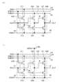
도 1은, 반도체 장치의 일례를 도시한다. 회로(100)는, 회로(110) 및 회로(120)를 갖는다. 회로(110)는, 배선(11), 배선(13), 배선(14), 배선(16), 및 회로(120)와 접속된다. 회로(120)는, 배선(11), 배선(12), 배선(15), 배선(16), 및 회로(110)와 접속된다. 다만, 본 실시형태의 일례는, 이것에 한정되지 않는다. 예를 들어, 회로(100), 회로(110) 및 회로(120)는 그 구성에 따라, 다양한 배선과 접속되는 것이 가능하다.Fig. 1 shows an example of a semiconductor device. The
회로(110)는 트랜지스터(111) 및 트랜지스터(112)를 갖는다. 회로(120)는, 트랜지스터(121), 트랜지스터(122), 트랜지스터(123), 및 트랜지스터(124)를 갖는다. 트랜지스터(121)의 제 1 단자는 배선(15)과 접속되고, 트랜지스터(121)의 제 2 단자는 배선(12)과 접속된다. 트랜지스터(122)의 제 1 단자는 배선(16)과 접속되고, 트랜지스터(122)의 제 2 단자는 배선(12)과 접속된다. 트랜지스터(123)의 제 1 단자는 배선(15)과 접속되고, 트랜지스터(123)의 제 2 단자는 트랜지스터(121)의 게이트와 접속되고, 트랜지스터(123)의 게이트는 배선(11)과 접속된다. 트랜지스터(124)의 제 1 단자는 배선(16)과 접속되고, 트랜지스터(124)의 제 2 단자는 트랜지스터(121)의 게이트와 접속되고, 트랜지스터(124)의 게이트는 트랜지스터(122)의 게이트와 접속된다. 트랜지스터(111)의 제 1 단자는, 배선(14)과 접속되고, 트랜지스터(111)의 제 2 단자는 트랜지스터(122)의 게이트와 접속되고, 트랜지스터(111)의 게이트는, 배선(13)과 접속된다. 트랜지스터(112)의 제 1 단자는, 배선(16)과 접속되고, 트랜지스터(112)의 제 2 단자는 트랜지스터(122)의 게이트와 접속되고, 트랜지스터(112)의 게이트는 배선(11)과 접속된다.The
또한, 트랜지스터(111)의 제 2 단자와, 트랜지스터(112)의 제 2 단자와, 트랜지스터(122)의 게이트와, 트랜지스터(124)의 게이트의 접속 개소를 노드 A로 나타내는 것으로 한다. 트랜지스터(121)의 게이트와 트랜지스터(123)의 제 2 단자와, 트랜지스터(124)의 제 2 단자의 접속 개소를 노드 B로 나타내는 것으로 한다.It is assumed that a node A represents a connection point of the second terminal of the
또한, 트랜지스터(111), 트랜지스터(112) 및 트랜지스터(121 내지 124)는, 각각 N채널형으로 한다. N채널형 트랜지스터는, 게이트와 소스 사이의 전위차가 임계 값 전압보다 크게 되었을 때에 온(ON)으로 된다. 그래서, 본 실시형태의 반도체 장치는, 비정질 반도체, 미결정 반도체, 산화물 반도체 또는 유기 반도체 등을 사용한 트랜지스터에 의하여 구성될 수 있다. 특히, 산화물 반도체를 사용한 트랜지스터에 의하여, 본 실시형태의 반도체 장치를 구성하는 것이 바람직하다. 왜냐하면, 반도체층으로서, 산화물 반도체를 사용하면, 트랜지스터의 이동도를 높게 할 수 있기 때문이다. 그래서, 본 실시형태의 반도체 장치를 해상도가 높은 표시 장치, 또는 대형의 표시 장치에 사용하는 것이 용이해진다. 다만, 본 실시형태의 일 형태는, 이것에 한정되지 않는다. 예를 들어, 트랜지스터(111), 트랜지스터(112) 및 트랜지스터(121 내지 124) 모두는, P채널형인 것이 가능하다. P채널형 트랜지스터는 게이트와 소스 사이의 전위차가 임계 값 전압보다 작게 되었을 때에 온으로 되는 것으로 한다.The
또한, 트랜지스터란, 게이트와, 드레인과, 소스를 포함하는 적어도 3개의 단자를 갖는 소자이다. 그리고, 드레인(드레인 영역 또는 드레인 전극)과 소스(소스 영역 또는 소스 전극) 사이에 채널 영역을 갖고, 드레인과 채널 영역과 소스를 통하여 전류를 흘릴 수 있다. 여기에서, 소스와 드레인이란, 트랜지스터의 구조 또는 동작 조건 등에 따라 바뀌기 때문에, 어느 것이 소스 또는 드레인인지를 한정하는 것이 어렵다. 그래서, 소스로서 기능하는 부분, 및 드레인으로서 기능하는 부분을, 소스 또는 드레인이라고 부르지 않는 경우가 있다. 그 경우, 일례로서, 소스와 드레인의 한쪽을, 제 1 단자, 제 1 전극, 또는 제 1 영역이라고 표기하고, 소스와 드레인의 다른 쪽을, 제 2 단자, 제 2 전극, 또는 제 2 영역이라고 표기하는 경우가 있다.A transistor is an element having at least three terminals including a gate, a drain, and a source. A channel region is provided between the drain (drain region or drain electrode) and the source (source region or source electrode), and current can flow through the drain, the channel region, and the source. Here, since the source and the drain vary depending on the structure and operating conditions of the transistor, it is difficult to limit which is the source or the drain. Therefore, a portion functioning as a source and a portion functioning as a drain may not be referred to as a source or a drain. In this case, for example, one of the source and the drain may be referred to as a first terminal, a first electrode, or a first region, and the other of the source and the drain may be referred to as a second terminal, a second electrode, May be indicated.
또한, X와 Y가 접속되어 있다고 명시적으로 기재하는 경우는 X와 Y가 전기적으로 접속되어 있는 경우와, X와 Y가 기능적으로 접속되어 있는 경우와, X와 Y가 직접 접속되어 있는 경우를 포함하는 것으로 한다. 여기서, X, Y는, 대상물(예를 들어 장치, 소자, 회로, 배선, 전극, 단자, 도전막, 층 등)인 것으로 한다. 따라서, 소정의 접속 관계, 예를 들어 도면이나 문장에 나타낸 접속 관계에 한정되지 않고, 도면이나 문장에 나타낸 접속 관계 이외의 것도 포함하는 것으로 한다.In the case where X and Y are explicitly described as being connected, the case where X and Y are electrically connected, the case where X and Y are functionally connected, the case where X and Y are directly connected . Here, X and Y are assumed to be objects (for example, devices, elements, circuits, wires, electrodes, terminals, conductive films, layers, etc.). Therefore, the present invention is not limited to a predetermined connection relationship, for example, a connection relationship shown in the drawings or a sentence, and includes connections other than those shown in the drawings or sentences.
배선(14)에는, 전압(VDD1)이 입력되는 것으로 한다. 전압(VDD1)은 일정한 전압으로 하고, 그라운드 전압보다 큰 값으로 한다. 그래서, 배선(14)은 전원선 또는 양 전원선으로서의 기능을 갖는다. 배선(15)에는, 전압(VDD2)이 입력되는 것으로 한다. 전압(VDD2)은 일정한 전압으로 하고, 전압(VDD1)보다 큰 값으로 한다. 그래서, 배선(15)은 전원선 또는 양 전원선으로서의 기능을 갖는다. 배선(16)에는, 전압(VSS)이 공급되는 것으로 한다. 전압(VSS)은 일정한 전압으로 하고, 전압(VDD1)보다 작은 값으로 한다. 그래서, 배선(16)은 전원선 또는 음 전원선으로서의 기능을 갖는다. 다만, 본 실시형태의 일례는, 이것에 한정되지 않는다. 예를 들어, 배선(14), 배선(15) 및/또는 배선(16)에는, 신호가 입력되는 것이 가능하다. 이와 같은 경우, 배선(14), 배선(15) 및/또는 배선(16)은 신호선으로서의 기능을 갖는 것이 가능하다. 다른 예로서, 전압(VSS)은 그라운드 전압과 대략 동일한 것이 가능하다. 그래서, 배선(16)은 그라운드선 또는 어스(earth) 등으로서의 기능을 갖는 것이 가능하다.It is assumed that the voltage VDD1 is input to the
배선(11)에는, 신호(IN1)가 입력되는 것으로 한다. 신호(IN1)는, 디지털 신호로 한다. 또한, 신호(IN1)의 H 레벨의 전위는, 대략 VDD1으로 하고, 신호(IN1)의 L 레벨의 전위는, 대략 VSS로 한다. 그래서 배선(11)은, 신호선으로서의 기능을 갖는다. 배선(13)에는, 신호(IN2)가 입력되는 것으로 한다. 신호(IN2)는, 디지털 신호로 한다. 또한, 신호(IN2)의 H 레벨의 전위는, 대략 VDD1으로 하고, 신호(IN2)의 L 레벨의 전위는, 대략 VSS로 한다. 그래서 배선(13)은, 신호선으로서의 기능을 갖는다. 다만, 본 실시형태의 일례는, 이것에 한정되지 않는다. 예를 들어, 배선(13)에는 전압(예를 들어, 전압(VDD1) 또는 전압(VDD2))이 입력되는 것이 가능하다. 이로써, 신호(IN2)를 생략할 수 있기 때문에, 신호의 개수 및 배선의 개수를 저감할 수 있다. 또한, 소비 전력의 삭감을 도모할 수 있다.It is assumed that the signal IN1 is input to the
배선(12)으로부터는, 신호(OUT)가 출력되는 것으로 한다. 신호(OUT)는, 디지털 신호로 하고, 회로(100)의 출력 신호로 한다. 그리고, 신호(OUT)의 H 레벨의 전위는, 대략 VDD2로 하고, 신호(OUT)의 L 레벨의 전위는, 대략 VSS로 한다. 즉, 신호(OUT)의 진폭 전압은 신호(IN1)의 진폭 전압보다 큰 것으로 한다. 그래서, 배선(12)은, 신호선으로서의 기능을 갖는다.It is assumed that the signal OUT is output from the
다음에, 본 실시형태에 있어서의 반도체 장치의 동작의 일례에 대하여 설명한다.Next, an example of the operation of the semiconductor device in the present embodiment will be described.
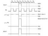
도 2는, 본 실시형태의 반도체 장치의 동작을 설명하기 위한 도면의 일례이다. 본 실시형태의 반도체 장치는, 신호(IN1) 및 신호(IN2)의 H 레벨과 L 레벨을 조합하여, 제 1 동작 내지 제 4 동작을 실현할 수 있다. 제 1 동작 내지 제 4 동작에 대하여 설명한다. 다만, 본 실시형태의 일례는, 이것에 한정되지 않는다. 예를 들어, 배선(14), 배선(15) 및/또는 배선(16)의 전위를 변화시킴으로써, 본 실시형태의 반도체 장치는, 더 많은 동작을 행하는 것이 가능하다.2 is an example of a diagram for explaining the operation of the semiconductor device of the present embodiment. The semiconductor device of the present embodiment can realize the first to fourth operations by combining the H level and the L level of the signal IN1 and the signal IN2. The first to fourth operations will be described. However, the present embodiment is not limited to this example. For example, by changing the potentials of the
우선, 제 1 동작에 대하여 설명한다(도 3a 참조). 제 1 동작에서는, 신호(IN1)가 H 레벨이 되고, 신호(IN2)가 L 레벨이 된다. 그래서, 트랜지스터(111)가 오프(OFF)로 되고, 트랜지스터(112)가 온으로 되기 때문에, 노드 A는 배선(16)과 도통 상태가 된다. 따라서, 노드 A에는 배선(16)의 전위(전압(VSS))가 공급되므로, 노드 A의 전위(전위(Va)라고 기재함)는, 대략 (VSS)이 된다. 그래서, 트랜지스터(124)가 오프로 된다. 이 때, 트랜지스터(123)는 온으로 되므로, 노드 B는 배선(15)과 도통 상태가 된다. 따라서, 노드 B에는 배선(15)의 전위(예를 들어, 전압(VDD2))가 공급되므로, 노드 B의 전위(전위(Vb)라고 기재함)는 상승되기 시작한다. 그 후, 노드 B의 전위가 (VSS+Vth121(Vth121: 트랜지스터(121)의 임계 값 전압))가 되면, 트랜지스터(121)가 온으로 된다. 이 때, 트랜지스터(122)는 오프로 되므로, 배선(12)은 배선(15)과 도통 상태가 된다. 따라서, 배선(12)에는, 배선(15)의 전위(예를 들어, 전압(VDD2))가 공급되므로, 배선(12)의 전위(신호(OUT))는 상승되기 시작한다. 그 후, 노드 B의 전위와 배선(12)의 전위는 계속하여 상승된다. 곧, 노드 B의 전위가 트랜지스터(123)의 게이트 전위(전압(VDD1))로부터 트랜지스터(123)의 임계 값 전압(Vth123)을 뺀 값이 된다. 그러면, 트랜지스터(123)는 오프로 되므로, 배선(15)과 노드 B는 비도통 상태가 된다. 그래서, 노드 B는 부유 상태가 된다. 이 때, 배선(12)의 전위는 계속하여 상승된다. 그래서, 노드 B의 전위는 트랜지스터(121)의 게이트와 제 2 단자의 사이의 기생 용량에 의하여, (VDD1-Vth123)로부터 더욱 상승된다. 이어서, 노드 B의 전위는 (VDD2+Vth121+V1(V1: 양의 수))가 된다. 소위, 부트스트랩 동작이다. 그래서, 배선(12)의 전위는 VDD2까지 상승될 수 있다. 이로써, 신호(OUT)는 H 레벨이 된다.First, the first operation will be described (see Fig. 3A). In the first operation, the signal IN1 becomes the H level and the signal IN2 becomes the L level. Thus, since the
다음에, 제 2 동작에 대하여 설명한다(도 3b 참조). 제 2 동작에서는, 신호(IN1)가 L 레벨이 되고, 신호(IN2)가 H 레벨이 된다. 그래서, 트랜지스터(111)가 온으로 되고, 트랜지스터(112)가 오프로 되기 때문에, 노드 A는 배선(14)과 도통 상태가 된다. 따라서, 노드 A에는 배선(14)의 전위(전압(VDD1))가 공급되므로, 노드 A의 전위는 상승된다. 그 후, 노드 A의 전위가 트랜지스터(111)의 게이트의 전위(H 레벨의 신호(IN2))로부터 트랜지스터(111)의 임계 값 전압(Vth111)을 뺀 값(VDD1-Vth111)가 된다. 따라서, 트랜지스터(111)는 오프로 되어, 배선(14)과 노드 A는 비도통 상태가 된다. 그래서, 노드 A는 부유 상태가 되고, 노드 A의 전위는 대략 (VDD1-Vth111)로 유지된다. 이로써, 트랜지스터(124)는 온으로 된다. 이 때, 트랜지스터(123)는 오프로 되므로, 노드 B는 배선(16)과 도통 상태가 된다. 따라서, 노드 B에는, 배선(16)의 전위(전압(VSS))가 공급되므로, 노드 B의 전위는 대략 VSS가 된다. 그래서, 트랜지스터(121)는, 오프로 된다. 이때, 트랜지스터(122)는 온으로 되므로, 배선(12)은 배선(16)과 도통 상태가 된다. 그러면, 배선(12)에는 배선(16)의 전위(전압(VSS))가 공급되므로, 배선(12)의 전위(신호(OUT))는 대략 VSS가 된다. 이로써, 신호(OUT)는 L 레벨이 된다.Next, the second operation will be described (see Fig. 3B). In the second operation, the signal IN1 becomes the L level and the signal IN2 becomes the H level. Thus, since the
다음에, 제 3 동작에 대하여 설명한다(도 4a 참조). 제 3 동작에서는, 신호(IN1)가 H 레벨이 되고, 신호(IN2)가 H 레벨이 된다. 그래서, 트랜지스터(111)가 온으로 되고, 트랜지스터(112)가 온으로 되기 때문에, 노드 A는 배선(14) 및 배선(16)과 도통 상태가 된다. 따라서, 노드 A에는 배선(14)의 전위(전압(VDD1))와 배선(16)의 전위(전압(VSS))가 공급되므로, 노드 A의 전위는 VSS와 VDD1 사이의 값이 된다. 이 노드 A의 전위는 트랜지스터(111)의 전류 공급 능력과 트랜지스터(112)의 전류 공급 능력에 의하여 결정된다. 여기서는, 트랜지스터(111)의 전류 공급 능력보다 트랜지스터(112)의 전류 공급 능력이 크다. 그래서, 바람직하게는, 노드 A의 전위는 VDD1보다 VSS에 가까운 값으로 한다. 보다 바람직하게는, 노드 A의 전위는 (VSS+Vth124(Vth124: 트랜지스터(124)의 임계 값 전압)) 또는 (VSS+Vth122(Vth122: 트랜지스터(122)의 임계 값 전압))보다 낮은 값으로 한다. 그래서, 트랜지스터(124)가 오프로 된다. 이 때, 트랜지스터(123)는 온으로 되므로, 노드 B는 배선(15)과 도통 상태가 된다. 따라서, 노드 B에는, 배선(15)의 전위(예를 들어, 전압(VDD2))가 공급되므로, 노드 B의 전위(전위(Vb)라고 함)는 상승되기 시작한다. 그 후, 노드 B의 전위가 (VSS+Vth121(Vth121: 트랜지스터(121)의 임계 값 전압))가 되면, 트랜지스터(121)가 온으로 된다. 이 때, 트랜지스터(122)는 오프로 되므로, 배선(12)은 배선(15)과 도통 상태가 된다. 그러면, 배선(12)에는 배선(15)의 전위(예를 들어, 전압(VDD2))가 공급되므로, 배선(12)의 전위(신호(OUT))는 상승되기 시작한다. 그 후, 노드 B의 전위와 배선(12)의 전위는 계속하여 상승된다. 이어서, 노드 B의 전위가 트랜지스터(123)의 게이트 전위(전압(VDD1))로부터 트랜지스터(123)의 임계 값 전압(Vth123)을 뺀 값이 된다. 따라서, 트랜지스터(123)는 오프로 되므로, 배선(15)과 노드 B는 비도통 상태가 된다. 따라서, 노드 B는 부유 상태가 된다. 이 때, 배선(12)의 전위는 계속하여 상승된다. 그래서, 노드 B의 전위는 트랜지스터(121) 게이트와 제 2 단자 사이의 기생 용량에 의하여, (VDD1-Vth123)로부터 더욱 상승된다. 이어서, 노드 B의 전위는 (VDD2+Vth121+V1(V1: 양의 수))가 된다. 소위, 부트스트랩 동작이다. 그래서, 배선(12)의 전위는 VDD2까지 상승될 수 있다. 이로써, 신호(OUT)는 H 레벨이 된다.Next, the third operation will be described (see Fig. 4A). In the third operation, the signal IN1 becomes the H level and the signal IN2 becomes the H level. Thus, the
다음에, 제 4 동작에 대하여 설명한다(도 4b 참조). 제 4 동작에서는, 신호(IN1)가 L 레벨이 되고, 신호(IN2)가 L 레벨이 된다. 그래서, 트랜지스터(111)가 오프로 되고, 트랜지스터(112)가 오프로 되므로, 노드 A는 부유 상태가 된다. 따라서, 노드 A의 전위는, 제 4 동작을 행하기 전의 상태인 채 유지된다. 예를 들어, 제 4 동작 전에 제 1 동작 또는 제 3 동작을 행하기로 한다. 이 경우, 노드 A의 전위는 대략 VSS가 된다. 한편, 제 4 동작 전에 제 2 동작으로 행하기로 한다. 이 경우, 노드 A의 전위는 대략 (VDD1-Vth111)가 된다. 여기서는, 제 4 동작을 행하기 전에 제 3 동작으로 행하기로 한다. 그래서, 노드 A의 전위는 대략 (VDD1-Vth111)로 유지되어 있다. 이로써, 트랜지스터(124)는 온으로 된다. 이 때, 트랜지스터(123)는 오프가 되므로, 노드 B는 배선(16)과 도통 상태가 된다. 따라서, 노드 B에는 배선(16)의 전위(전압(VSS))가 공급되므로, 노드 B의 전위는 대략 VSS가 된다. 그래서, 트랜지스터(121)는 오프로 된다. 이 때, 트랜지스터(122)는 온으로 되므로, 배선(12)은 배선(16)과 도통 상태가 된다. 따라서, 배선(12)에는, 배선(16)의 전위(전압(VSS))이 공급되므로, 배선(12)의 전위(신호(OUT))는 대략 VSS가 된다. 이로써, 신호(OUT)는 L 레벨이 된다.Next, the fourth operation will be described (see Fig. 4B). In the fourth operation, the signal IN1 becomes the L level and the signal IN2 becomes the L level. Thus, the
상술한 바와 같이, 본 실시형태의 반도체 장치는, 신호(IN1)의 진폭 전압을 크게 하여 출력할 수 있다. 구체적으로는, 신호(IN1)의 진폭 전압을 높게 하여 출력할 수 있다. 이로써, 본 실시형태의 반도체 장치에 신호(IN1)를 출력하는 회로(시프트 레지스터 회로, 디코더 회로 등)의 진폭 전압을 작게 할 수 있다. 그래서, 상기 회로의 소비 전력을 작게 할 수 있다. 또는, 상기 회로를 구성하는 트랜지스터에 인가되는 전압을 작게 할 수 있다. 그래서, 상기 트랜지스터의 열화 또는 파괴를 억제할 수 있다.As described above, the semiconductor device of the present embodiment can output the signal IN1 with an increased amplitude voltage. Specifically, the amplitude of the signal IN1 can be increased and output. Thus, the amplitude voltage of the circuit (shift register circuit, decoder circuit, etc.) for outputting the signal IN1 to the semiconductor device of the present embodiment can be reduced. Thus, the power consumption of the circuit can be reduced. Alternatively, the voltage applied to the transistors constituting the circuit can be reduced. Therefore, deterioration or destruction of the transistor can be suppressed.
또한, 신호(OUT)의 반전하는 타이밍을, 신호(IN1)의 반전하는 타이밍과 대략 일치시킬 수 있다. 이로써, 배선(12)에 인버터 회로 등을 형성할 필요가 없게 된다. 그래서, 소비 전력의 삭감, 회로 규모의 축소, 또는 레이아웃 면적의 축소를 도모할 수 있다.Further, the timing of inverting the signal OUT can be made substantially coincident with the timing of inverting the signal IN1. Thereby, it becomes unnecessary to form an inverter circuit or the like in the
또한, 제 1 동작에 있어서, 신호(IN1)가 H 레벨일 때 신호(IN2)가 L레벨이 됨으로써, 배선(14)과 배선(16) 사이의 관통 전류를 방지할 수 있다. 이로써, 소비 전력을 작게 할 수 있다.In addition, in the first operation, when the signal IN1 is at the H level, the signal IN2 becomes the L level, thereby preventing the penetration current between the
또한, 제 1 동작 내지 제 4 동작에 대하여 설명하였지만, 본 실시형태의 반도체 장치는 이들 모든 동작을 행할 필요는 없다는 것을 부기한다. 본 실시형태의 반도체 장치는, 이들 복수의 동작 중에서 필요한 동작만을 선택하고, 그 선택한 동작을 행하는 것이 가능하다.Although the first to fourth operations have been described, it is noted that the semiconductor device of this embodiment need not perform all these operations. The semiconductor device of the present embodiment can select only necessary operations among the plurality of operations, and can perform the selected operation.
다음에, 본 실시형태의 반도체 장치에 있어서, 도 1과 상이한 구성에 대하여 설명한다.Next, the configuration of the semiconductor device of the present embodiment, which is different from that of FIG. 1, will be described.
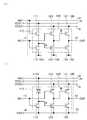
우선, 도 5a 및 도 5b에 도시하는 바와 같이, 도 1에 도시하는 반도체 장치에 있어서, 트랜지스터(111)의 제 1 단자는 배선(14)과는 다른 배선과 접속되는 것이 가능하다. 도 5a는, 트랜지스터(111)의 제 1 단자가 배선(15)과 접속되는 경우의 반도체 장치의 일례를 도시한다. 이로써, 전압(VDD1)을 생략할 수 있다. 또는, 트랜지스터(111)의 소스와 드레인간의 전위차(Vgs)를 크게 할 수 있으므로, 노드 A의 전위의 상승 시간을 짧게 할 수 있다. 도 5b는 트랜지스터(111)의 제 1 단자가 배선(13)과 접속되는 경우의 반도체 장치의 일례를 도시한다. 그래서, 전압(VDD1)을 생략할 수 있다. 또는, 트랜지스터(111)에 역 바이어스를 인가할 수 있으므로, 트랜지스터(111)의 열화를 억제할 수 있다. 다만, 본 실시형태의 일례는 이것에 한정되지 않는다. 예를 들어, 트랜지스터(111)의 제 1 단자는 신호(IN1)의 반전 신호가 입력되는 배선과 접속되는 것이 가능하다.First, as shown in FIGS. 5A and 5B, in the semiconductor device shown in FIG. 1, the first terminal of the
다음에, 도 6a 및 도 6b에 도시하는 바와 같이, 도 1, 도 5a 및 도 5b에 도시하는 반도체 장치에 있어서, 트랜지스터(111)의 게이트는, 배선(13)과는 다른 배선과 접속되는 것이 가능하다. 도 6a는, 트랜지스터(111)의 게이트가 배선(15)과 접속되는 경우의 반도체 장치의 일례를 도시한다. 이로써, 신호(IN2)를 생략할 수 있다. 그래서, 소비 전력의 삭감을 도모할 수 있다. 도 6b는, 트랜지스터(111)의 게이트가 배선(14)과 접속되는 경우의 반도체 장치의 일례를 도시한다. 이로써, 신호(IN2)를 생략할 수 있다. 그래서, 소비 전력의 삭감을 도모할 수 있다. 다만, 본 실시형태의 일례는 이것에 한정되지 않는다. 예를 들어, 트랜지스터(111)의 게이트는, 신호(IN1)의 반전 신호가 입력되는 배선과 접속되는 것이 가능하다.Next, as shown in Figs. 6A and 6B, in the semiconductor device shown in Figs. 1, 5A and 5B, the gate of the
다음에, 도 7a에 도시하는 바와 같이, 도 1, 도 5a 내지 도 6b에 도시하는 반도체 장치에 있어서, 트랜지스터(111)의 제 1 단자는, 배선(14)과는 다른 배선과 접속되고, 또 트랜지스터(111)의 게이트는, 배선(13)과는 다른 배선과 접속되는 것이 가능하다. 도 7a는, 트랜지스터(111)의 제 1 단자가 배선(13)과 접속되고, 트랜지스터(111)의 게이트가 배선(14)과 접속되는 경우의 반도체 장치의 일례를 도시한다. 이로써, 제 2 동작에 있어서, 노드 A의 전위를 상승시키고, 제 4 동작에 있어서 노드 A의 전위를 감소시킬 수 있다. 그래서, 제 2 동작에 있어서, 트랜지스터(122) 및 트랜지스터(124)가 온으로 되고, 제 4 동작에 있어서 트랜지스터(122) 및 트랜지스터(124)가 오프로 된다. 이로써, 트랜지스터(122) 및 트랜지스터(124)가 온으로 되는 시간을 짧게 할 수 있다. 그래서, 트랜지스터(122) 및 트랜지스터(124)의 열화를 억제할 수 있다.Next, as shown in Fig. 7A, in the semiconductor device shown in Figs. 1 and 5A to 6B, the first terminal of the
다음에, 도 7b 및 도 8a에 도시하는 바와 같이, 도 1, 도 5a 내지 도 7a에 도시하는 반도체 장치에 있어서, 트랜지스터(123)의 제 1 단자는, 배선(15)과는 다른 배선과 접속되는 것이 가능하다. 도 7b는 트랜지스터(123)의 제 1 단자가 배선(13B)과 접속되는 경우의 반도체 장치의 일례를 도시한다. 배선(13B)에는, 신호(IN2B)가 입력되는 것으로 한다. 신호(IN2B)는, 신호(IN2)의 반전 신호이다. 이로써, 트랜지스터(123)에 역 바이어스를 인가할 수 있으므로, 트랜지스터의 열화를 억제할 수 있다. 도 8a는, 트랜지스터(123)의 제 1 단자가 배선(11)과 접속되는 경우의 반도체 장치의 일례를 도시한다. 이로써, 제 2 동작 및 제 4 동작에 있어서, 트랜지스터(123)에 인가되는 소스와 드레인간의 전위차(Vds)를 작게 할 수 있다. 그래서, 트랜지스터(123)의 열화를 억제할 수 있다. 또는, 트랜지스터(123)의 오프 전류를 작게 할 수 있고, 소비 전력의 삭감을 도모할 수 있다. 다만, 본 실시형태의 일례는, 이것에 한정되지 않는다. 예를 들어, 트랜지스터(123)의 제 1 단자는, 배선(14)과 접속되는 것이 가능하다.Next, as shown in Figs. 7B and 8A, in the semiconductor device shown in Figs. 1 and 5A to 7A, the first terminal of the
또한, 도 8b에 도시하는 바와 같이, 트랜지스터(123)의 제 1 단자가 배선(11)과 접속되는 경우, 트랜지스터(123)의 게이트는 배선(11)과는 다른 배선과 접속되는 것이 가능하다. 도 8b는, 트랜지스터(123)의 게이트가 배선(14)과 접속되는 경우의 반도체 장치의 일례를 도시한다. 다만, 본 실시형태의 일례는, 이것에 한정되지 않는다. 트랜지스터(123)의 게이트는, 배선(15), 신호(IN2)의 반전 신호가 입력되는 배선, 또는 신호(IN2)과는 상이한 위상의 신호가 입력되는 배선 등과 접속되는 것이 가능하다.8B, when the first terminal of the
다음에, 도 9a에 도시하는 바와 같이, 도 1, 도 5a 내지 도 8b에 도시하는 반도체 장치에 있어서, 트랜지스터(121)의 게이트와 제 2 단자 사이에 용량 소자(125)를 형성하는 것이 가능하다. 이로써, 제 1 동작 및 제 2 동작에 있어서, 노드 B의 전위를 더욱 상승시킬 수 있다. 따라서, 트랜지스터(121)의 게이트와 소스간의 전위차(Vgs)를 크게 할 수 있으므로, 신호(OUT)의 상승 시간을 짧게 할 수 있다.Next, as shown in Fig. 9A, in the semiconductor device shown in Figs. 1 and 5A to 8B, it is possible to form the capacitor 125 between the gate of the
다음에, 도 9b에 도시하는 바와 같이, 도 1, 도 5a 내지 도 9a에 도시하는 반도체 장치에 있어서, 노드 A와 배선(16) 사이에 용량 소자(126)를 형성하는 것이 가능하다. 이로써, 제 4 동작에 있어서, 노드 A의 전위의 변동, 노드 A의 노이즈 등을 억제할 수 있으므로, 노드 A의 전위를 유지하기 쉬워진다. 다만, 본 실시형태의 일례는, 이것에 한정되지 않는다. 예를 들어, 용량 소자(126)는 노드 A와 배선(16)은 다른 배선(예를 들어, 배선(13), 배선(14), 또는 배선(15) 등) 사이에 접속되는 것이 가능하다. 특히, 용량 소자(126)가 노드 A와 배선(13) 사이에 접속됨으로써, 노드 A의 전위를 신호(IN2)에 동기시켜 변동시킬 수 있다. 그래서, 트랜지스터(122) 및 트랜지스터(124)가 온으로 되는 시간을 짧게 할 수 있다.Next, as shown in Fig. 9B, in the semiconductor device shown in Figs. 1 and 5A to 9A, it is possible to form the capacitive element 126 between the node A and the
다음에, 도 10a에 도시하는 바와 같이, 도 1, 도 5a 내지 도 9b에 도시하는 반도체 장치에 있어서, 각 트랜지스터 등은, 각각 다른 배선과 접속되는 것이 가능하다. 도 10a는, 트랜지스터(112)의 제 1 단자와, 트랜지스터(124)의 제 2 단자와, 트랜지스터(122)의 제 2 단자가 각각 다른 배선과 접속되는 경우의 반도체 장치의 일례를 도시한다. 배선(16)은, 배선(16A), 배선(16B), 배선(16C)이라는 복수의 배선으로 분할된다. 또한, 트랜지스터(112)의 제 1 단자, 트랜지스터(124)의 제 2 단자 및 트랜지스터(122)의 제 2 단자는 각각, 배선(16A), 배선(16B), 배선(16C)과 접속된다. 다만, 본 실시형태의 일례는, 이것에 한정되지 않는다. 예를 들어, 트랜지스터(121)의 제 1 단자와, 트랜지스터(123)의 제 1 단자도 각각 다른 배선과 접속되는 것이 가능하다. 이 경우, 배선(15)을 2개의 배선으로 분할하는 것이 가능하다.Next, as shown in Fig. 10A, in the semiconductor device shown in Figs. 1 and 5A to 9B, transistors and the like can be connected to different wirings. 10A shows an example of a semiconductor device in which a first terminal of the
다음에, 도 10b에 도시하는 바와 같이, 도 1, 도 5a 내지 도 10a에 도시하는 반도체 장치에 있어서, 트랜지스터는 저항 소자, 다이오드, 용량 소자 등과 치환하는 것이 가능하다. 도 10b는 트랜지스터(111)를 다이오드(111d)로 치환하는 경우의 반도체 장치를 도시한다. 다이오드(111d)의 한쪽의 전극(예를 들어, 양극)은, 배선(13)과 접속되고, 다른 쪽의 전극(예를 들어, 음극)은, 노드 A와 접속된다. 다만, 본 실시형태의 일례는, 이것에 한정되지 않는다. 예를 들어, 트랜지스터(111)는, 저항 소자와 치환하는 것이 가능하다. 상기 저항 소자는, 배선(13 내지 15) 중 어느 하나와 노드 A 사이에 접속되는 것이 가능하다. 다른 예로서, 트랜지스터(123)는 한쪽의 전극(예를 들어, 양극)이 배선(11)과 접속되고, 다른 쪽의 전극(예를 들어, 음극)이 노드 B와 접속되는 다이오드와 치환하는 것이 가능하다. 다른 예로서, 다이오드는 다이오드 접속의 트랜지스터인 것이 가능하다.Next, as shown in Fig. 10B, in the semiconductor device shown in Figs. 1 and 5A to 10A, the transistor can be replaced with a resistance element, a diode, a capacitive element, or the like. 10B shows a semiconductor device in which the
다음에, 각 회로의 기능의 일례, 및 각 트랜지스터의 기능의 일례에 대하여 설명한다.Next, an example of the function of each circuit and an example of the function of each transistor will be described.
우선, 회로(100)는 신호(IN1)의 진폭 전압을 크게 하는 기능을 갖는다. 또는, 회로(100)는 신호(IN1)의 H 레벨의 전위를 상승시키는 기능을 갖는다. 또는, 회로(100)는 신호(IN1)가 반전되면, 신호(OUT)를 반전시키는 기능을 갖는다. 또는, 회로(100)는 신호(IN1)가 H 레벨이 되면, 신호(OUT)를 H 레벨로 하는 기능을 갖는다. 또는, 회로(100)는 신호(IN1)가 L 레벨이 되면, 신호(OUT)를 L 레벨로 하는 기능을 갖는다. 이와 같이, 회로(100)는 레벨 시프터 회로로서의 기능을 갖는다.First, the
또한, 전압(VDD2)을 전압(VDD1)보다 작게 함으로써, 신호(OUT)의 H 레벨의 전위를 신호(IN1) 또는 신호(IN2)의 H 레벨의 전위보다 낮게 할 수 있다. 이 경우, 회로(100)는 신호(IN1)의 진폭 전압을 작게 하는 기능을 갖는다.Also, by making the voltage VDD2 smaller than the voltage VDD1, the H level potential of the signal OUT can be made lower than the H level potential of the signal IN1 or IN2. In this case, the
다음에, 회로(110)는 신호(IN1)를 반전하는 기능을 갖는다. 또는, 회로(110)는 신호(IN1)가 H 레벨이 되면 노드 A의 전위를 감소시키는 기능을 갖는다. 또는, 회로(110)는 신호(IN1)가 L 레벨이 되면 노드 A의 전위를 상승시키는 기능을 갖는다. 또는, 회로(110)는 노드 A를 부유 상태로 하는 기능을 갖는다. 이와 같이, 회로(110)는 인버터 회로로서의 기능을 갖는다.Next, the
다음에, 회로(120)는 신호(IN1)의 진폭 전압을 크게 하는 기능을 갖는다. 또는, 회로(120)는 신호(IN1)의 H 레벨의 전위를 상승시키는 기능을 갖는다. 또는, 회로(120)는 신호(IN1)가 반전되면, 신호(OUT)를 반전시키는 기능을 갖는다. 또는, 회로(120)는 신호(IN1)가 H 레벨이 되면, 신호(OUT)를 H 레벨로 하는 기능을 갖는다. 또는, 회로(120)는 신호(IN1)가 L 레벨이 되면, 신호(OUT)를 L 레벨로 하는 기능을 갖는다. 이와 같이, 회로(120)는 레벨 시프터 회로로서의 기능을 갖는다.Next, the
다음에, 트랜지스터(111)는, 배선(14)과 노드 A의 도통 상태를 제어하는 기능을 갖는다. 또는, 트랜지스터(111)는, 배선(14)의 전위를 노드 A에 공급하는 타이밍을 제어하는 기능을 갖는다. 또는, 트랜지스터(111)는, 노드 A의 전위를 상승시키는 타이밍을 제어하는 기능을 갖는다. 또는, 트랜지스터(111)는, 노드 A를 부유 상태로 하는 타이밍을 제어하는 기능을 갖는다. 이와 같이, 트랜지스터(111)는 스위치로서의 기능을 갖는다.Next, the
다음에, 트랜지스터(112)는, 배선(16)과 노드 A의 도통 상태를 제어하는 기능을 갖는다. 또는, 트랜지스터(112)는, 배선(16)의 전위를 노드 A에 공급하는 타이밍을 제어하는 기능을 갖는다. 또는, 트랜지스터(112)는, 노드 A의 전위를 감소시키는 타이밍을 제어하는 기능을 갖는다. 이와 같이, 트랜지스터(112)는 스위치로서의 기능을 갖는다.Next, the
다음에, 트랜지스터(121)는, 배선(15)과 배선(12)의 도통 상태를 제어하는 기능을 갖는다. 또는, 트랜지스터(121)는, 배선(15)의 전위를 배선(12)에 공급하는 타이밍을 제어하는 기능을 갖는다. 또는, 트랜지스터(121)는, 배선(12)의 전위를 상승시키는 타이밍을 제어하는 기능을 갖는다. 또는, 트랜지스터(121)는, 부트스트랩 동작을 행하는 타이밍을 제어하는 기능을 갖는다. 또는, 트랜지스터(121)는, 노드 B의 전위를 상승시키는 타이밍을 제어하는 기능을 갖는다. 이와 같이, 트랜지스터(121)는 스위치로서의 기능을 갖는다.Next, the
다음에, 트랜지스터(122)는, 배선(16)과 배선(12)의 도통 상태를 제어하는 기능을 갖는다. 또는, 트랜지스터(122)는 배선(16)의 전위를 배선(12)에 공급하는 타이밍을 제어하는 기능을 갖는다. 또는, 트랜지스터(122)는 배선(12)의 전위를 감소시키는 타이밍을 제어하는 기능을 갖는다. 이와 같이, 트랜지스터(122)는 스위치로서의 기능을 갖는다.Next, the
다음에, 트랜지스터(123)는, 배선(15)과 노드 B의 도통 상태를 제어하는 기능을 갖는다. 또는, 트랜지스터(123)는 배선(14)의 전위를 노드 B에 공급하는 타이밍을 제어하는 기능을 갖는다. 또는, 트랜지스터(123)는 노드 B의 전위를 상승시키는 타이밍을 제어하는 기능을 갖는다. 또는, 트랜지스터(123)는 노드 B를 부유 상태로 하는 타이밍을 제어하는 기능을 갖는다. 이와 같이, 트랜지스터(123)는 스위치로서의 기능을 갖는다.Next, the
다음에, 트랜지스터(124)는, 배선(16)과 노드 B의 도통 상태를 제어하는 기능을 갖는다. 또는, 트랜지스터(124)는 배선(16) 의 전위를 노드 B에 공급하는 타이밍을 제어하는 기능을 갖는다. 또는, 트랜지스터(124)는 노드 B의 전위를 감소시키는 타이밍을 제어하는 기능을 갖는다. 이와 같이, 트랜지스터(124)는 스위치로서의 기능을 갖는다.Next, the
다음에, 각 트랜지스터의 채널 폭의 일례에 대하여 설명한다.Next, an example of the channel width of each transistor will be described.
우선, 트랜지스터(121)의 채널 폭은, 트랜지스터(111), 트랜지스터(112), 및 트랜지스터(122 내지 124)의 채널 폭보다 큰 것이 바람직하다. 즉, 회로(100)가 갖는 트랜지스터 중에서 가장 큰 것이 바람직하다. 왜냐하면, 트랜지스터(121)는 배선(12)을 구동하는 역할을 가짐으로써, 큰 구동 능력을 필요로 하기 때문이다. 또한, 트랜지스터(121)의 채널 폭은 트랜지스터(123)의 채널 폭의 2배 이상 10배 이하인 것이 바람직하다. 보다 바람직하게는, 3배 이상 8배 이하이다. 보다 바람직하게는, 4배 이상 6배 이하이다.The channel width of the
다음에, 트랜지스터(122)의 채널 폭은 트랜지스터(111), 트랜지스터(112), 트랜지스터(113) 및 트랜지스터(124)의 채널 폭보다 큰 것이 바람직하다. 왜냐하면, 트랜지스터(122)는 배선(12)을 구동하는 역할을 가짐으로써, 큰 구동 능력을 필요로 하기 때문이다. 또한, 트랜지스터(122)의 채널 폭은 트랜지스터(124)의 채널 폭의 2배 이상 30배 이하인 것이 바람직하다. 보다 바람직하게는, 4배 이상 15배 이하이다. 보다 바람직하게는, 6배 이상 10배 이하이다.Next, it is preferable that the channel width of the
또한, 트랜지스터(122)의 채널 폭은 트랜지스터(121)의 채널 폭보다 큰 것이 가능하다.It is also possible that the channel width of the
트랜지스터(123)의 채널 폭은, 트랜지스터(124)의 채널 폭보다도 큰 것이 바람직하다. 왜냐하면, 제 1 동작 및 제 3 동작에 있어서, 타이밍의 불일치에 의하여 트랜지스터(123)와 트랜지스터(124)가 동시에 온으로 되어도, 노드 B의 전위를 상승시킬 수 있게 하기 위해서이다. 또한, 트랜지스터(123)의 채널 폭은, 트랜지스터(124)의 채널 폭의 1.5배 이상 10배 이하인 것이 바람직하다. 보다 바람직하게는, 2배 이상 8배 이하이다. 보다 바람직하게는, 2.5배 이상 5배 이하이다.The channel width of the
또한, 트랜지스터의 채널 폭에 의하여, 트랜지스터의 전류 공급 능력을 제어할 수 있다. 구체적으로는, 트랜지스터의 채널 폭이 클수록 트랜지스터의 전류 공급 능력은 향상된다. 다만, 트랜지스터의 전류 공급 능력을 제어하는 인자(因子)는, 트랜지스터의 채널 폭에 한정되지 않는다. 예를 들어, 트랜지스터의 채널 길이 또는 트랜지스터의 게이트와 소스간의 전위차(Vgs)에 의하여, 전류 공급 능력을 제어할 수 있다. 구체적으로는, 트랜지스터의 채널 길이가 작을수록 트랜지스터의 전류 공급 능력은 향상된다. 그리고, 트랜지스터의 게이트와 소스간의 전위차(Vgs)가 클수록 트랜지스터의 전류 공급 능력은 향상된다. 그 외에도 트랜지스터를 멀티 게이트 구조로 함으로써, 전류 공급 능력을 저하시킬 수 있다.Further, the current supply capability of the transistor can be controlled by the channel width of the transistor. Specifically, the larger the channel width of the transistor, the better the current supply capability of the transistor is. However, the factor for controlling the current supply capability of the transistor is not limited to the channel width of the transistor. For example, the current supply capability can be controlled by the channel length of the transistor or the potential difference (Vgs) between the gate and the source of the transistor. Specifically, the smaller the channel length of the transistor, the more the current supply capability of the transistor is improved. The larger the potential difference Vgs between the gate and the source of the transistor, the better the current supply capability of the transistor is. In addition, by making the transistor a multi-gate structure, the current supply capability can be lowered.
상술한 바와 같이, 트랜지스터의 전류 공급 능력을 제어하는 방법은 복수 존재한다. 그래서, 이하에 있어서 트랜지스터의 전류 공급 능력을 제어하는 방법으로서 채널 폭을 제어하는 방법이 예시되어 있는 경우, 상기 채널 폭을 채널 길이 또는 트랜지스터의 게이트와 소스간의 전위차(Vgs) 등으로 바꿔 말하는 것이 가능하다.As described above, there are a plurality of methods for controlling the current supply capability of the transistor. Therefore, in the following, when a method of controlling the channel width is exemplified as a method of controlling the current supply capability of the transistor, it is possible to change the channel width to a channel length or a potential difference (Vgs) between the gate and the source of the transistor Do.
(실시형태 2)(Embodiment 2)
본 실시형태에서는 반도체 장치의 일례, 및 그 반도체 장치의 구동 방법의 일례에 대하여 설명한다. 본 실시형태의 반도체 장치는 실시형태 1의 반도체 장치를 갖는다.In the present embodiment, an example of a semiconductor device and an example of a method of driving the semiconductor device will be described. The semiconductor device of the present embodiment has the semiconductor device of the first embodiment.
우선, 본 실시형태의 반도체 장치의 일례에 대하여 설명한다.First, an example of the semiconductor device of the present embodiment will be described.
도 11은, 본 실시형태의 반도체 장치의 일례를 도시한다. 도 11에 도시하는 반도체 장치는, 회로(300), 회로(400), 및 회로(500)를 갖는다. 회로(400)는, 회로(401_1 내지 401_m(m은 자연수))를 갖는다. 그리고, 회로(401_1 내지 401_m)로서, 각각, 실시형태에서 서술하는 반도체 장치를 사용할 수 있다. 도 11에서는, 회로(401_1 내지 401_m)로서 각각, 도 1에 도시하는 반도체 장치가 사용되는 것으로 한다. 회로(500)는, 회로(501) 및 회로(502)를 갖는다.11 shows an example of the semiconductor device of the present embodiment. The semiconductor device shown in FIG. 11 has a
회로(300)는, 배선(21_1 내지 21_m), 배선(23), 배선(24_1 내지 24_4), 배선(25) 및 배선(27)과 접속된다. 회로(400)는, 배선(21_1 내지 21_m), 배선(22_1 내지 22_m), 배선(24_1 내지 24_4), 배선(25), 배선(26) 및 배선(27)과 접속된다. 회로(400_i)(i는 1 내지 m의 어느 하나)는, 배선(21_i), 배선(22_i), 배선(24_1 내지 24_4) 중의 어느 하나, 배선(25), 배선(26) 및 배선(27)과 접속된다. 그리고, 회로(401_i)에 있어서, 배선(11), 배선(12), 배선(13), 배선(14), 배선(15) 및 배선(16)은 각각 배선(21_i), 배선(22_i), 배선(24_1 내지 24_4) 중의 어느 하나, 배선(25), 배선(26) 및 배선(27)과 접속된다. 회로(500)는, 배선(23), 배선(24_1 내지 24_4), 배선(25), 배선(26) 및 배선(27)과 접속된다. 회로(501)는, 배선(23) 및 배선(24_1 내지 24_4)과 접속되고, 회로(502)는, 배선(25), 배선(26) 및 배선(27)과 접속된다.The
또한, 회로(400_i)가 배선(24_1)과 접속된다고 가정한다. 이 경우, 회로(401_i+1), 회로(401_i+2), 회로(401_i+3)는 각각, 배선(24_2), 배선(24_3), 배선(24_4)과 접속되는 경우가 많다. 또는 회로(401_i-3), 회로(401_i-2), 회로(401_i-1)는 각각 배선(24_2), 배선(24_3), 배선(24_4)과 접속되는 경우가 많다.It is also assumed that the circuit 400_i is connected to the wiring 24_1. In this case, the circuit 401_i + 1, the circuit 401_i + 2, and the circuit 401_i + 3 are often connected to the wiring 24_2, the wiring 24_3, and the wiring 24_4, respectively. Or the circuit 401_i-3, the circuit 401_i-2 and the circuit 401_i-1 are connected to the wiring 24_2, the wiring 24_3 and the wiring 24_4, respectively.
또한, 회로(401_i)는 배선(24_1 내지 24_4) 중, 신호(SOUTi)가 H 레벨이 되는 기간에 있어서, 그 전위가 L 레벨이 되는 배선과 접속되는 것이 바람직하다. 이로써, 트랜지스터(111)와 트랜지스터(112)가 동시에 온으로 되는 기간을 생략할 수 있다. 그래서, 소비 전력의 삭감을 도모할 수 있다.It is preferable that the circuit 401_i is connected to a wiring whose potential becomes the L level in a period in which the signal SOUTi becomes H level among the wirings 24_1 to 24_4. Thus, the period in which the
회로(500)는, 회로(300) 및 회로(400)에 신호 또는 전압 등을 공급하는 타이밍을 제어하는 기능을 갖는다. 그리고, 회로(500)는 회로(300) 및 회로(400)가 동작하는 타이밍을 제어하는 기능을 갖는다. 즉, 회로(500)는 컨트롤러로서의 기능을 갖는다.The
회로(501)는, 배선(23) 및 배선(24_1 내지 24_4)에 각각 신호(SP), 신호(CK1), 신호(CK2), 신호(CK3), 신호(CK4)를 출력하는 타이밍을 제어하는 기능을 갖는다. 즉, 회로(501)는 신호 생성 회로(또는 타이밍 제너레이터라고도 함)로서의 기능을 갖는다. 그래서, 회로(501)는 스위치, 다이오드, 트랜지스터, 발진 회로, 클록제너레이터, PLL 회로 및/또는 분주 회로 등을 가질 수 있다.The
도 12에 도시하는 바와 같이, 신호(SP), 신호(CK1), 신호(CK2), 신호(CK3) 및 신호(CK4)는, 디지털 신호인 경우가 많다. 이들 신호의 H 레벨의 전위는, 대략 VDD1로 하고, L 레벨의 전위는, 대략 VSS로 한다. 그리고, 신호(SP)는 스타트 펄스(또는 수평 동기 신호, 수직 동기 신호라고도 함)로서의 기능을 갖는다. 그래서, 배선(23)은, 신호선(또는 스타트 신호선이라고도 함)으로서의 기능을 갖는다. 신호(CK1), 신호(CK2), 신호(CK3) 및 신호(CK4)는 각각 클록 신호로서의 기능을 갖는다. 신호(CK1), 신호(CK2), 신호(CK3) 및 신호(CK4)는 위상이 1/4주기(90°)씩 어긋나는 것으로 한다. 그래서, 배선(24_1 내지 24_4)은 클록 신호선(또는 신호선이라고도 함)으로서의 기능을 갖는다.As shown in Fig. 12, the signal SP, the signal CK1, the signal CK2, the signal CK3, and the signal CK4 are often digital signals. The H level potential of these signals is approximately VDD1, and the L level potential is approximately VSS. The signal SP has a function as a start pulse (also referred to as a horizontal synchronizing signal or a vertical synchronizing signal). Thus, the
또한, 도 12에 도시하는 바와 같이, 신호(CK1), 신호(CK2), 신호(CK3) 및 신호(CK4)는 평형인 것으로 한다. “평형”이란, 1주기 중, H 레벨이 되는 기간과, L 레벨이 되는 기간이 대략 같은 것을 가리킨다. 다만, 본 실시형태의 일례는, 이것에 한정되지 않는다. 예를 들어, 도 13a에 도시하는 바와 같이, 신호(CK1), 신호(CK2), 신호(CK3) 및 신호(CK4)는 비평형인 것이 가능하다. 비평형이란, H 레벨이 되는 기간과 L 레벨이 되는 기간이 상이한 것을 가리킨다. 또한, 여기서 “상이하다”는 것은, 대략 같은 경우의 범위 이외의 것으로 한다.It is assumed that the signal CK1, the signal CK2, the signal CK3, and the signal CK4 are balanced as shown in Fig. The term " balanced type " indicates that the period of H level and the period of L level are approximately the same in one cycle. However, the present embodiment is not limited to this example. For example, as shown in Fig. 13A, the signal CK1, the signal CK2, the signal CK3, and the signal CK4 can be non-planar. The non-planar type indicates that the H level is different from the L level. It is to be noted that the term " different "
또한, 도 13b 및 도 13c에 도시하는 바와 같이, 본 실시형태의 반도체 장치에는, 단상(單相)의 클록 신호를 사용하는 것이 가능하다. 이 경우에도, 클록 신호는 도 13b에 도시하는 바와 같이, 평형인 것이 가능하고, 도 13c에 도시하는 바와 같이, 비평형인 것이 가능하다. 다만, 본 실시형태의 일례는, 이것에 한정되지 않는다. 예를 들어, 본 실시형태의 반도체 장치에는, 3상의 클록 신호 또는 5상의 클록 신호를 사용하는 것이 가능하다.As shown in Figs. 13B and 13C, a single-phase clock signal can be used for the semiconductor device of this embodiment. In this case as well, the clock signal can be balanced, as shown in Fig. 13B, and can be non-planar, as shown in Fig. 13C. However, the present embodiment is not limited to this example. For example, a three-phase clock signal or a five-phase clock signal can be used in the semiconductor device of the present embodiment.
회로(502)는, 배선(25), 배선(26) 및 배선(27)에 각각 전압(VDD1), 전압(VDD2), 전압(VSS)을 출력하는 기능을 갖는다. 즉, 회로(502)는 전원 회로(또는 레귤레이터(regulator)라고도 함)로서의 기능을 갖는다. 그래서, 배선(25)은 전원선 또는 양의 전원선으로서의 기능을 갖는다. 배선(27)은, 전원선, 음의 전원선, 그라운드 선, 또는 어스(earth) 등으로서의 기능을 갖는다. 그래서, 회로(502)는 스위치, 트랜지스터, 용량 소자, 코일, 다이오드, 레귤레이터, DCDC 컨버터 및/또는 승압 회로 등을 가질 수 있다.The
또한, 회로(500), 회로(501) 및 회로(502)는, 회로(300) 및 회로(400)의 구성에 따라, 회로(300) 및 회로(400)에 다양한 신호 또는 다양한 전압을 공급하는 것이 가능하다.The
회로(300)는, 회로(500)로부터 공급되는 신호 및 전압(예를 들어, 신호(SP), 신호(CK1 내지 CK4), 전압(VDD1) 및 전압(VSS))에 따라, 신호(SOUT1 내지 SOUTm)를 출력하는 타이밍을 제어하는 기능을 갖는다. 신호(SOUT1 내지 SOUTm)는, 디지털 신호인 경우가 많고, 그 H 레벨의 전위는 대략 VDD1로 하고, 그 L 레벨의 전위는 대략 VSS로 한다. 그리고, 회로(300)는, 신호(SOUT1 내지 SOUTm)를 순차적으로 H 레벨로 하는 기능을 갖는다. 즉, 회로(300)는 시프트 레지스터 회로로서의 기능을 갖는다. 다만, 본 실시형태의 일례는, 이것에 한정되지 않는다. 예를 들어, 회로(300)는 신호(SOUT1 내지 SOUTm)를 임의의 순서로 H 레벨로 하는 기능을 갖는 것이 가능하다. 그래서, 회로(300)는 디코더 회로로서의 기능을 갖는 것이 가능하다.
또한, 신호(SOUT1 내지 SOUTm)는, 각각 배선(21_1 내지 21_m)을 통하여 회로(400)에 입력된다. 예를 들어, 신호(SOUTi)는 배선(21_i)을 통하여 회로(401_i)에 입력된다. 그래서, 배선(21_1 내지 21_m)은 각각 신호선으로서의 기능을 갖는다.Further, the signals SOUT1 to SOUTm are inputted to the
또한, 도 12에 도시하는 타이밍 차트에서는, 신호(SOUTi)가 H 레벨이 되는 기간의 일부와, 신호(SOUTi-1)가 H 레벨이 되는 기간의 일부가 중복된다. 그리고, 신호(SOUTi)가 H 레벨이 되는 기간의 일부와, 신호(SOUTi+1)가 H 레벨이 되는 기간의 일부가 중복된다. 이로써, 신호(SOUTi 내지 SOUTm)가 H 레벨이 되는 기간을 길게 할 수 있다. 그래서, 회로(300)의 구동 주파수를 느리게 할 수 있으므로, 소비 전력의 삭감을 도모할 수 있다. 다만, 본 실시형태의 일례는, 이것에 한정되지 않는다. 예를 들어, 도 13a 내지 도 13c에 도시하는 바와 같이, 신호(SOUT1 내지 SOUTm)가 각각 H 레벨이 되는 기간은 중복되지 않는 것이 가능하다.In the timing chart shown in Fig. 12, a part of the period in which the signal SOUTi becomes the H level and a part of the period in which the signal SOUTi-1 becomes the H level are overlapped. A part of the period in which the signal SOUTi becomes the H level and a part of the period in which the signal SOUTi + 1 becomes the H level are overlapped. This makes it possible to lengthen the period in which the signals SOUTi to SOUTm are at the H level. Thus, since the driving frequency of the
회로(400)는, 회로(300)로부터 공급되는 신호(예를 들어, 신호(SOUTi 내지 SOUTm))와, 회로(500)로부터 공급되는 신호 및 전압(예를 들어, 신호(CK1 내지 CK4), 전압(VDD1), 전압(VDD2) 및 전압(VSS))에 따라, 신호(BOUT1 내지 BOUTm)를 출력하는 타이밍을 제어하는 기능을 갖는다. 신호(BOUT1 내지 BOUTm)는, 디지털 신호인 경우가 많고, 그 H 레벨의 전위는 대략 (VDD2)로 하고, 그 L 레벨의 전위는 대략 (VSS)로 한다. 그리고, 신호(BOUT1 내지 BOUTm)가 반전하는 타이밍은, 신호(SOUT1 내지 SOUTm)가 반전하는 타이밍과 대략 같은 것으로 한다. 즉, 회로(400)는, 신호(SOUT1 내지 SOUTm)의 진폭 전압을 크게 하는 기능을 갖는다.The
다음에, 본 실시형태에서의 반도체 장치의 동작의 일례에 대하여 설명한다.Next, an example of the operation of the semiconductor device in the present embodiment will be described.
도 14는, 회로(401_i)의 타이밍 차트의 일례이다. 도 14에는, 신호(SOUTi), 신호(CK), 회로(401_i)의 노드 A의 전위, 회로(401_i)의 노드 B의 전위, 및 신호(BOUTi)를 도시한다. 신호(CK)는, 신호(CK1 내지 CK4) 중, 신호(SOUTi)가 H 레벨이 될 때 L 레벨이 되는 신호로 한다. 그리고, 도 14에 도시하는 타이밍 차트는, 기간(Ta), 기간(Tb) 및 기간(Tc)을 갖는다. 도 14에 도시하는 타이밍 차트 중, 기간(Ta) 이외에는 기간(Tb)과 기간(Tc)이 순차적으로 배치된다.14 is an example of a timing chart of the circuit 401_i. Fig. 14 shows signals SOUTi, CK, the potential of the node A of the circuit 401_i, the potential of the node B of the circuit 401_i, and the signal BOUTi. The signal CK is a signal that becomes L level when the signal SOUTi becomes H level, among the signals CK1 to CK4. The timing chart shown in Fig. 14 has a period Ta, a period Tb, and a period Tc. In the timing chart shown in Fig. 14, the period Tb and the period Tc are sequentially arranged other than the period Ta.
또한, 신호(SOUTi)는, 도 2에 도시하는 신호(IN1)에 대응하는 것으로 한다. 신호(CK)는, 도 2에 도시하는 신호(IN2)에 대응하는 것으로 한다. 신호(BOUTi)는, 도 2에 도시하는 신호(OUT)에 대응하는 것으로 한다.It is assumed that the signal SOUTi corresponds to the signal IN1 shown in Fig. It is assumed that the signal CK corresponds to the signal IN2 shown in Fig. The signal BOUTi corresponds to the signal OUT shown in Fig.
우선, 기간(Ta)에 있어서, 신호(SOUTi)가 H 레벨이 되고, 신호(CK)가 L 레벨이 된다. 따라서, 회로(400_i)는, 제 1 동작을 행한다. 그래서, 신호(BOUTi)는 H 레벨이 된다. 이로써, 신호(SOUTi)의 H 레벨의 전위를 VDD1으로부터 VDD2까지 상승시킬 수 있다.First, in the period Ta, the signal SOUTi becomes H level and the signal CK becomes L level. Therefore, the circuit 400_i performs the first operation. Thus, the signal BOUTi becomes H level. As a result, the potential of the H level of the signal SOUTi can be raised from VDD1 to VDD2.
다음에, 기간(Tb)에 있어서, 신호(SOUTi)가 L 레벨이 되고, 신호(CK)가 H 레벨이 된다. 따라서, 회로(400_i)는, 제 2 동작을 행한다. 그래서, 신호(BOUTi)는 L 레벨이 된다.Next, in the period Tb, the signal SOUTi becomes L level, and the signal CK becomes H level. Therefore, the circuit 400_i performs the second operation. Thus, the signal BOUTi becomes L level.
다음에, 기간(Tc)에 있어서, 신호(SOUTi)가 L 레벨이 되고, 신호(CK)가 L 레벨이 된다. 따라서, 회로(400_i)는, 제 4 동작을 행한다. 또한, 기간(Tc) 전은, 기간(Tb)이기 때문에, 전위(Va)는 (VDD-Vth115)를 유지한다. 그래서, 신호(BOUTi)는 L 레벨인 채 유지된다.Next, in the period Tc, the signal SOUTi becomes L level, and the signal CK becomes L level. Therefore, the circuit 400_i performs the fourth operation. Since the period Tc is before the period Tc, the potential Va maintains (VDD-Vth115). Thus, the signal BOUTi remains at the L level.
상술한 바와 같이, 본 실시형태의 반도체 장치는 회로(300)의 출력 신호의 진폭 전압을 크게 하고 나서, 출력할 수 있다. 이로써, 회로(300)의 진폭 전압을 작게 할 수 있다. 그래서, 회로(300)의 소비 전력을 삭감할 수 있다.As described above, the semiconductor device of this embodiment can output the amplitude of the output signal of the
또는, 회로(401_1 내지 401_m)는 각각, 제 1 동작과 제 2 동작과 제 4 동작의 어느 하나를 행하는 것이 많다. 그래서, 트랜지스터(111)와 트랜지스터(112)가 동시에 온으로 되는 기간이 없으므로, 소비 전력의 삭감을 도모할 수 있다.Alternatively, the circuits 401_1 to 401_m often perform the first operation, the second operation and the fourth operation, respectively. Thus, since there is no period in which the
다음에, 회로(300)의 일례에 대하여 설명한다.Next, an example of the
도 15는, 회로(300)의 일례를 도시한다. 회로(300)는, 회로(310_1 내지 310_m)를 갖는다. 회로(310_i)는, 배선(21_i), 배선(21_i-1), 배선(21_i+2), 배선(24_1 내지 24_4) 중 어느 3개, 배선(25) 및 배선(27)과 접속되는 것으로 한다. 다만, 회로(310_1)는, 배선(21_i-1) 대신에 배선(23)과 접속되는 경우가 많다.Fig. 15 shows an example of the
회로(310_1 내지 310_m)는, 각각 트랜지스터(311), 트랜지스터(312), 트랜지스터(313), 트랜지스터(314), 트랜지스터(315), 트랜지스터(316), 트랜지스터(317), 트랜지스터(318), 및 트랜지스터(319)를 갖는다. 트랜지스터(311)의 제 1 단지는 배선(33)과 접속되고, 트랜지스터(311)의 제 2 단자는 배선(32)과 접속된다. 트랜지스터(312)의 제 1 단자는 배선(37)과 접속되고, 트랜지스터(312)의 제 2 단자는 배선(32)과 접속되고, 트랜지스터(312)의 게이트는, 배선(35)과 접속된다. 트랜지스터(313)의 제 1 단자는, 배선(37)과 접속되고, 트랜지스터(313)의 제 2 단자는 배선(32)과 접속된다. 트랜지스터(314)의 제 1 단자는, 배선(37)과 접속되고, 트랜지스터(314)의 제 2 단자는 트랜지스터(311)의 게이트와 접속되고, 트랜지스터(314)의 게이트는 트랜지스터(313)의 게이트와 접속된다. 트랜지스터(315)의 제 1 단자는, 배선(36)과 접속되고, 트랜지스터(315)의 제 2 단자는 트랜지스터(311)의 게이트와 접속되고, 트랜지스터(315)의 게이트는 배선(31)과 접속된다. 트랜지스터(316)의 제 1 단자는, 배선(36)과 접속되고, 트랜지스터(316)의 제 2 단자는, 트랜지스터(313)의 게이트와 접속되고, 트랜지스터(316)의 게이트는 배선(38)과 접속된다. 트랜지스터(317)의 제 1 단자는, 배선(36)과 접속되고, 트랜지스터(317)의 게이트는 배선(35)과 접속된다. 트랜지스터(318)의 제 1 단자는, 트랜지스터(317)의 제 2 단자와 접속되고, 트랜지스터(318)의 제 2 단자는 트랜지스터(313)의 게이트와 접속되고, 트랜지스터(318)의 게이트는 배선(34)와 접속된다. 트랜지스터(319)의 제 1 단자는, 배선(37)과 접속되고, 트랜지스터(319)의 제 2 단자는, 트랜지스터(313)의 게이트와 접속되고, 트랜지스터(319)의 게이트는 배선(31)과 접속된다.The circuits 310_1 to 310_m are connected to the
또한, 트랜지스터(311)의 게이트와, 트랜지스터(314)의 제 2 단자와, 트랜지스터(315)의 제 2 단자의 접속 개소를 노드 C로 나타낸다. 트랜지스터(313)의 게이트와, 트랜지스터(314)의 게이트와, 트랜지스터(316)의 제 2 단자와, 트랜지스터(318)의 제 2 단자와, 트랜지스터(319)의 제 2 단자의 접속 개소를 노드 D로 나타낸다.The connection point between the gate of the
또한, 트랜지스터(311 내지 319)는, N채널형이다. 그래서, 본 실시형태의 반도체 장치를 모두 N채널형 트랜지스터에 의하여 구성할 수 있다. 다만, 본 실시형태의 일례는, 이것에 한정되지 않는다. 예를 들어, 트랜지스터(311 내지 319) 모두는, P채널형인 것이 가능하다.The
또한, 회로(310_i)에 있어서, 배선(31)은 배선(21_i-1)과 접속된다. 배선(32)은 배선(21_i)과 접속된다. 배선(33 내지 35)은 배선(24_1 내지 24_4) 중 선택된 3개의 배선과 접속된다. 예를 들어, 배선(33)이 배선(24_1)과 접속된다고 하면, 배선(34)은 배선(24_2)과 접속되고, 배선(35)은 배선(24_3)과 접속된다. 배선(36)은 배선(25)과 접속된다. 배선(37)은 배선(27)과 접속된다. 배선(38)은 배선(21_i+2)과 접속된다. 다만, 회로(310_1)에 있어서는, 배선(31)은 배선(23)과 접속된다.In the circuit 310_i, the
다음에, 회로(300)의 동작의 일례에 대하여 설명한다.Next, an example of the operation of the
도 16은, 회로(310_i)에 사용할 수 있는 타이밍 차트의 일례를 도시한다. 도 16에 도시하는 타이밍 차트는, 신호(IN33), 신호(IN34), 신호(IN35), 신호(SOUTi-1), 신호(SOUTi+1), 노드 C의 전위(전위(Vc)), 노드 D의 전위(전위(Vd)) 및 신호(SOUTi)를 도시한다. 그리고, 도 16에 도시하는 타이밍 차트는, 기간(T1 내지 T9)을 갖는다. 기간(T5 내지 T9)이 순차적으로 배치되고, 그 이외의 기간에 기간(T1 내지 T4)이 순차적으로 반복하여 배치되는 것으로 한다.Fig. 16 shows an example of a timing chart that can be used in the circuit 310_i. The timing chart shown in Fig. 16 is a timing chart of the signal IN33, the signal IN34, the signal IN35, the signal SOUTi-1, the signal SOUTi + 1, the potential of the node C (potential Vc) (Potential Vd) of the signal D and the signal SOUTi. The timing chart shown in Fig. 16 has periods T1 to T9. The periods T5 to T9 are sequentially arranged, and the periods T1 to T4 are sequentially and repeatedly arranged in other periods.
우선, 기간(T1)에 있어서, 신호(SOUTi)가 L 레벨이 되고, 신호(SOUTi+2)가 L 레벨이 되고, 신호(IN33)가 L 레벨이 되고, 신호(IN34)가 H 레벨이 되고, 신호(IN35)가 H 레벨이 된다. 그래서, 트랜지스터(316)가 오프로 되고, 트랜지스터(317)가 온으로 되고, 트랜지스터(318)가 온으로 되고, 트랜지스터(319)가 오프로 되므로, 노드 D는 배선(36)과 도통 상태가 된다. 따라서, 노드 D에는 배선(36)의 전위(예를 들어, 전압(VDD))가 공급되므로, 노드 D의 전위는 상승된다. 그래서, 트랜지스터(314)는 온으로 된다. 이 때, 트랜지스터(315)는 오프로 되므로, 노드 C는 배선(37)과 도통 상태가 된다. 따라서, 노드 C에는 배선(37)의 전위(전압(VSS))가 공급되므로, 노드 C의 전위는 대략 VSS가 된다. 그래서, 트랜지스터(311)는 오프로 된다. 이 때, 트랜지스터(312) 및 트랜지스터(313)는 온으로 되므로, 배선(32)은 배선(37)과 도통 상태가 된다. 따라서, 배선(32)에는 배선(37)의 전위(전압(VSS))가 공급되므로, 배선(32)의 전위는 대략 VSS가 된다. 그래서, 신호(SOUTi)는 L 레벨이 된다.First, in the period T1, the signal SOUTi becomes L level, the signal SOUTi + 2 becomes L level, the signal IN33 becomes L level, and the signal IN34 becomes H level , The signal IN35 becomes H level. Thus, the
다음에, 기간(T2)에서는, 기간(T1)과 비교하여 신호(IN34)가 L 레벨이 되는 점이 상이하다. 그래서, 트랜지스터(318)가 오프로 되므로, 배선(36)과 노드 D와는 비도통 상태가 된다. 따라서, 노드 D는 부유 상태가 되므로, 노드 D의 전위는 기간(T1)에 있어서의 전위를 유지한다.Next, the period T2 is different from the period T1 in that the signal IN34 becomes L level. Thus, since the transistor 318 is turned off, the
다음에, 기간(T3)에서는, 기간(T2)과 비교하여 신호(IN33)가 H 레벨이 되고, 신호(IN35)가 L 레벨이 되는 점이 상이하다. 그래서, 트랜지스터(317) 및 트랜지스터(312)가 오프로 된다.Next, in the period T3, the signal IN33 becomes H level and the signal IN35 becomes L level in comparison with the period T2. Thus, the transistor 317 and the
다음에, 기간(T4)에서는, 기간(T3)과 비교하여 신호(IN34)가 H 레벨이 되는 점이 상이하다. 그래서, 트랜지스터(318)가 온으로 된다.Next, in the period T4, the signal IN34 becomes H level in comparison with the period T3. Thus, the transistor 318 is turned on.
다음에, 기간(T5)에서는, 신호(SOUTi)가 H 레벨이 되고, 신호(SOUTi+2)가 L 레벨이 되고, 신호(IN33)가 L 레벨이 되고, 신호(IN34)가 L 레벨이 되고, 신호(IN35)가 H 레벨이 된다. 그래서, 트랜지스터(316)는 오프로 되고, 트랜지스터(317)가 온으로 되고, 트랜지스터(318)가 오프로 되고, 트랜지스터(319)는 온으로 되므로, 배선(37)과 노드 D는 도통 상태가 된다. 따라서, 노드 D에는 배선(37)의 전위(전압(VSS))가 공급되므로, 노드 D의 전위는 대략 VSS가 된다. 그래서, 트랜지스터(314)는 오프로 된다. 이 때, 트랜지스터(315)는 온으로 되므로, 노드 C는 배선(36)과 도통 상태가 된다. 따라서, 노드 C에는 배선(36)의 전위가 공급되므로, 노드 C의 전위는 상승되기 시작된다. 이어서, 노드 C의 전위가 배선(32)의 전위(VSS)와 트랜지스터(311)의 임계 값 전압(Vth311)의 합(VSS+Vth311)이 된다. 따라서, 트랜지스터(311)가 온으로 된다. 이 때, 트랜지스터(312)는 온으로 되고, 트랜지스터(313)는 오프로 되므로, 배선(32)은 배선(37) 및 배선(33)과 도통 상태가 된다. 따라서, 배선(32)에는 배선(37)의 전위(전압(VSS))와 배선(33)의 전위(L 레벨의 신호(IN33))가 공급되므로, 배선(37)의 전위는 대략 (VSS)가 된다. 그래서, 신호(SOUTi)는 L 레벨이 된다. 그 후, 노드 C의 전위는 계속하여 상승된다. 이어서, 노드 C의 전위가 (VDD1-Vth315(Vth315는 트랜지스터(315)의 임계 값 전압))가 된다. 따라서, 트랜지스터(315)는 오프로 되고, 노드 C는 부유 상태가 된다. 그래서, 노드 C의 전위는 (VDD1-Vth315)로 유지된다.Next, in the period T5, the signal SOUTi becomes H level, the signal SOUTi + 2 becomes L level, the signal IN33 becomes L level, and the signal IN34 becomes L level , The signal IN35 becomes H level. Thus, the
다음에, 기간(T6)에서는, 신호(SOUTi-1)는 H 레벨인 채 유지되고, 신호(SOUTi+2)는 L 레벨인 채 유지되고, 신호(IN33)가 H 레벨이 되고, 신호(IN34)가 L 레벨인 채 유지되고, 신호(IN35)가 L 레벨이 된다. 그래서, 트랜지스터(316)가 오프인 채 유지되고, 트랜지스터(317)가 오프로 되고, 트랜지스터(318)는 오프인 채 유지되고, 트랜지스터(319)는 온인 채 유지되므로, 노드 D는 배선(37)과 도통 상태인 채 유지된다. 따라서, 노드 D에는 배선(37)의 전위(전압(VSS))가 공급된 채 유지되므로, 노드 D의 전위는 대략 VSS인 채 유지된다. 그래서, 트랜지스터(314)는 오프인 채 유지된다. 이 때, 트랜지스터(315)는 오프인 채 유지된다. 따라서, 노드 C는 부유 상태가 되므로, 노드 C의 전위는 (VDD1- Vth315)인 채 유지된다. 따라서, 트랜지스터(311)는 온인 채 유지된다. 그리고, 트랜지스터(312) 및 트랜지스터(313)는 오프로 되므로, 배선(32)은 배선(33)과 도통 상태가 된다. 이 때, 신호(IN33)가 H 레벨이 되므로, 배선(32)의 전위는 상승되기 시작한다. 동시에, 노드 C의 전위도 부트스트랩 동작에 의하여 상승된다. 결과적으로, 노드 C의 전위는 (VDD1- Vth311(Vth311은 트랜지스터(311)의 임계 값 전압))+V1까지 상승된다. 배선(32)의 전위는 대략 VDD1까지 상승된다. 따라서, 신호(SOUTi)는 H 레벨이 된다.Next, in the period T6, the signal SOUTi-1 is held at the H level, the signal SOUTi + 2 is held at the L level, the signal IN33 is at the H level, and the signal IN34 Is maintained at the L level, and the signal IN35 becomes the L level. Thus, since the
다음에, 기간(T7)에서는, 신호(SOUTi-1)가 L 레벨이 되고, 신호(IN34)가 H 레벨이 되는 점이 기간(T6)과 비교하여 상이하다. 그래서, 트랜지스터(318)가 온으로 되고, 트랜지스터(319)가 오프로 된다. 따라서, 노드 D는 부유 상태가 되므로, 노드 D의 전위는 대략 VSS로 유지된다.Next, in the period T7, the point that the signal SOUTi-1 becomes the L level and the signal IN34 becomes the H level differs from the period T6. Thus, the transistor 318 is turned on and the
다음에, 기간(T8)에서는, 신호(SOUTi-1)가 L 레벨인 채 유지되고, (SOUTi+2)는 H 레벨이 되고, 신호(IN33)가 L 레벨이 되고, 신호(IN34)가 H 레벨인 채 유지되고, 신호(IN35)가 H 레벨이 되므로, 트랜지스터(316)가 온으로 되고, 트랜지스터(317)가 온으로 되고, 트랜지스터(318)가 온으로 되고, 트랜지스터(319)가 오프인 채 유지되므로, 노드 D는 배선(36)과 도통 상태가 된다. 따라서, 노드 D에는 배선(36)의 전위(전압(VDD1))가 공급되므로, 노드 D의 전위는 상승된다. 그래서, 트랜지스터(314)가 온으로 된다. 이 때, 트랜지스터(315)는 오프인 채 유지되므로, 노드 C는 배선(37)과 도통 상태가 된다. 따라서, 노드 C에는 배선(37)의 전위(전압(VSS))가 공급되므로, 노드 C의 전위는 대략 VSS가 된다. 따라서, 트랜지스터(311)는 오프로 된다. 이 때, 트랜지스터(312) 및 트랜지스터(313)는 온으로 되므로, 배선(32)은 배선(33) 및 배선(37)과 도통 상태가 된다. 따라서, 배선(32)에는 배선(37)의 전위(전압(VSS))가 공급되므로 배선(32)의 전위는 대략 VSS가 된다. 따라서, 신호(OUTi)는 L 레벨이 된다.Next, in the period T8, the signal SOUTi-1 remains at the L level, the signal SOUTi + 2 becomes the H level, the signal IN33 becomes the L level, and the signal IN34 becomes H The
다음에, 기간(T9)에서는, 기간(T8)과 비교하여 신호(IN34)가 L 레벨이 되는 점이 상이하다. 그래서, 트랜지스터(318)가 오프로 된다.Next, the period T9 differs from the period T8 in that the signal IN34 becomes L level. Thus, the transistor 318 is turned off.
이상, 회로(300)의 일례에 대하여 설명하였다.An example of the
또한, 트랜지스터(317)의 게이트가 배선(34)과 접속되고, 트랜지스터(318)의 게이트가 배선(35)과 접속되는 것이 가능하다.It is also possible that the gate of the transistor 317 is connected to the
또한, 트랜지스터(319)가 생략되는 것이 가능하다.It is also possible that the
또한, 트랜지스터(312)가 생략되는 것이 가능하다.It is also possible that the
(실시형태 3)(Embodiment 3)
본 실시형태에서는, 표시 장치의 일례 및 표시 장치가 갖는 화소의 일례에 대하여 설명한다. 특히, 액정 표시 장치 및 액정 표시 장치가 갖는 화소의 일례에 대하여 설명한다. 또한, 본 실시형태의 표시 장치의 구동 회로는, 실시형태 1 및 실시형태 2의 반도체 장치를 갖는 것이 가능하다.In the present embodiment, an example of a display device and an example of a pixel included in the display device will be described. In particular, an example of a pixel of a liquid crystal display device and a liquid crystal display device will be described. Further, the drive circuit of the display device of the present embodiment can have the semiconductor device of the first embodiment and the second embodiment.
우선, 본 실시형태의 표시 장치의 일례에 대하여 설명한다.First, an example of the display device of the present embodiment will be described.
도 17a는, 본 실시형태의 표시 장치의 일례를 도시한다. 도 17a에 도시하는 표시 장치는, 회로(1001), 회로(1002), 회로(1003_1), 화소(1004), 및 단자(1005)를 갖는다. 화소(1004)에는, 회로(1003_1)로부터 복수의 배선이 연장되어 배치되는 것으로 한다. 상기 복수의 배선은, 게이트 신호선(또는 주사선이라고도 함)으로서의 가능을 갖는다. 또는, 화소(1004)에는, 회로(1002)로부터 복수의 배선이 연장되어 배치되는 것으로 한다. 상기 복수의 배선은, 비디오 신호선(또는 데이터선이라고도 함)으로서의 기능을 갖는다. 또한, 회로(1003_1)로부터 연장되어 배치되는 복수의 배선과, 회로(1002)로부터 연장되어 배치되는 복수의 배선에 대응하여, 복수의 화소가 배치된다. 다만, 본 실시형태의 일례는, 이것에 한정되지 않는다. 예를 들어, 화소부(1004)에는, 이외에도 다양한 배선이 배치되는 것이 가능하다. 상기 배선은, 게이트 신호선, 데이터선, 전원선, 또는 용량선 등으로서의 기능을 갖는 것이 가능하다.17A shows an example of the display device of the present embodiment. The display device shown in Fig. 17A has a
도 17a에 도시하는 표시 장치에서는, 회로(1003_1)가 화소부(1004)와 같은 기판(1006)에 형성되고, 회로(1001) 및 회로(1002)가 화소부(1004)와 다른 기판에 형성되는 것으로 한다. 회로(1003_1)의 구동 주파수는, 회로(1001) 또는 회로(1002)와 비교하여 느린 경우가 많다. 그래서, 트랜지스터의 반도체층으로서, 비결정 반도체, 비정질 반도체, 미결정 반도체, 산화물 반도체, 유기 반도체 등을 사용하는 것이 용이하게 된다. 결과적으로, 표시 장치를 크게 할 수 있다. 또는, 표시 장치를 싸게 제작할 수 있다.In the display device shown in Fig. 17A, the circuit 1003_1 is formed on a
회로(1001)는, 회로(1002) 및 회로(1003_1)에 신호, 전압 또는 전류 등을 공급하는 타이밍을 제어하는 기능을 갖는다. 또는, 회로(1001)는, 회로(1002) 및 회로(1003_1)를 제어하는 기능을 갖는다. 이와 같이, 회로(1001)는 컨트롤러, 제어 회로, 타이밍 발생기, 전원 회로, 또는 레귤레이터 등으로서의 기능을 갖는다.The
회로(1002)는, 비디오 신호를 화소부(1004)에 공급하는 타이밍을 제어하는 기능을 갖는다. 또는, 회로(1002)는 화소부(1004)가 갖는 화소의 휘도 또는 투과율 등을 제어하는 기능을 갖는다. 이와 같이, 회로(1002)는 구동 회로, 소스 드라이버 회로 또는 신호선 구동 회로 등으로서의 기능을 갖는다.The
회로(1003_1)는, 게이트 신호를 화소부(1004)에 공급하는 타이밍을 제어하는 기능을 갖는다. 또는 회로(1003_1)는 화소를 선택하는 타이밍을 제어하는 기능을 갖는다. 이와 같이, 회로(1003_1)는 게이트 드라이버(또는 주사선 구동 회로라고도 함)로서의 기능을 갖는다.The circuit 1003_1 has a function of controlling the timing of supplying the gate signal to the
또는, 도 17b에 도시하는 바와 같이, 본 실시형태의 표시 장치는, 회로(1003_2)를 갖는 것이 가능하다. 회로(1003_2)는, 회로(1003_1)와 마찬가지의 기능을 갖는다. 그리고, 회로(1003_1)와 회로(1003_2)에 의하여, 같은 배선을 구동함으로써, 회로(1003_1) 및 회로(1003_2)의 부하를 작게 할 수 있다. 다만, 본 실시형태의 일례는, 이것에 한정되지 않는다. 예를 들어, 회로(1003_1)가 홀수번째 단의 게이트 신호선을 구동하고, 회로(1003_2)가 짝수번째 단의 게이트 신호선을 구동하는 것이 가능하다. 이로써, 회로(1003_1) 및 회로(1003_2)의 구동 주파수를 작게 할 수 있다. 다른 예로서, 본 실시형태의 표시 장치는 회로(1003_1)와 마찬가지의 기능을 갖는 회로를, 3개 이상 갖는 것이 가능하다.Alternatively, as shown in Fig. 17B, the display device of the present embodiment can have the circuit 1003_2. The circuit 1003_2 has the same function as the circuit 1003_1. The loads of the circuits 1003_1 and 1003_2 can be reduced by driving the same wiring by the circuits 1003_1 and 1003_2. However, the present embodiment is not limited to this example. For example, it is possible that the circuit 1003_1 drives the odd-numbered gate signal lines, and the circuit 1003_2 drives the even-numbered gate signal lines. This makes it possible to reduce the driving frequencies of the circuits 1003_1 and 1003_2. As another example, the display device of the present embodiment can have three or more circuits having the same function as the circuit 1003_1.
또한, 도 17b에 도시하는 표시 장치에서는, 회로(1003_1) 및 회로(1003_2)가 화소부(1004)와 같은 기판(1006)에 형성되고, 회로(1001) 및 회로(1002)가 화소부(1004)와 다른 기판에 형성되는 것으로 한다. 회로(1003_1) 및 회로(1003_2)의 구동 주파수는, 회로(1001) 또는 회로(1002)와 비교하여 느린 경우가 많다. 그래서, 트랜지스터의 반도체층으로서, 비결정 반도체, 비정질 반도체, 미결정 반도체, 산화물 반도체, 유기 반도체 등을 사용하는 것이 용이하게 된다. 결과적으로, 표시 장치를 크게 할 수 있다. 또는, 표시 장치를 싸게 제작할 수 있다.17B, the circuit 1003_1 and the circuit 1003_2 are formed on a
또한, 도 17c에 도시하는 바와 같이 회로(1002), 회로(1003_1) 및 회로(1003_2)가 화소부(1004)와 같은 기판(1006)에 형성되고, 회로(1001)가 화소부(1004)와 다른 기판에 형성되는 것이 가능하다. 이로써, 외부 회로를 삭감할 수 있으므로, 신뢰성의 향상, 제작 비용의 삭감 또는 수율의 향상을 도모할 수 있다.17C, the
또한, 도 17d에 도시하는 바와 같이 회로(1002)의 일부의 회로(1002a), 회로(1003_1) 및 회로(1003_2)가 화소부(1004)와 같은 기판(1006)에 형성되고, 회로(1002)의 다른 부분의 회로(1002b)가 화소부(1004)와 다른 기판에 형성되는 것이 가능하다. 회로(1002a)로서는, 스위치, 시프트 레지스터 및/또는 셀렉터 등의 비교적으로 구동 주파수가 낮은 회로를 사용하는 것이 가능하다. 이로써, 트랜지스터의 반도체층으로서, 비결정 반도체, 비정질 반도체, 미결정 반도체, 산화물 반도체, 유기 반도체 등을 사용하는 것이 용이하게 된다. 결과적으로, 표시 장치를 크게 할 수 있다. 또는 표시 장치를 싸게 제작할 수 있다.17D, a
또한, 회로(1003_1), 회로(1003_2), 회로(1002) 및/또는 회로(1002a)의 일부로서, 실시형태 1 및 실시형태 2의 반도체 장치를 사용하는 것이 가능하다. 이로써, 구동 전압을 작게 할 수 있으므로, 소비 전력의 삭감을 도모할 수 있다.It is also possible to use the semiconductor devices of the first and second embodiments as a part of the circuit 1003_1, the circuit 1003_2, the
다음에, 화소부(1004)가 갖는 화소의 일례에 대하여 설명한다.Next, an example of a pixel included in the
도 17e는, 화소의 일례를 도시한다. 화소(3020)는, 트랜지스터(3021), 액정 소자(3022) 및 용량 소자(3023)를 갖는다. 트랜지스터(3021)의 제 1 단자는, 배선(3031)과 접속되고, 트랜지스터(3021)의 제 2 단자는, 액정 소자(3022)의 한쪽의 전극 및 용량 소자(3023)의 한쪽의 전극과 접속되고, 트랜지스터(3021)의 게이트는, 배선(3032)와 접속된다. 액정 소자(3022)의 다른 쪽의 전극은, 전극(3034)과 접속되고, 용량 소자(3023)의 다른 쪽의 전극은, 배선(3033)과 접속된다.17E shows an example of a pixel. The
배선(3031)에는, 도 17a 내지 도 17d에 도시하는 회로(1002)로부터 비디오 신호가 입력되는 것으로 한다. 따라서, 배선(3031)은 비디오 신호선(또는 소스 신호선이라고도 함)으로서의 기능을 갖는다. 배선(3032)에는, 도 17a 내지 도 17d에 도시하는 회로(1003_1) 및/또는 회로(1003_2)로부터 게이트 신호가 입력되는 것으로 한다. 따라서, 배선(3032)은 게이트 신호선으로서의 기능을 갖는다. 배선(3033) 및 배선(3034)에는, 도 17a 내지 도 17d에 도시하는 회로(1001)로부터 일정한 전압이 공급되는 것으로 한다. 따라서, 배선(3033)은, 전원선 또는 용량선으로서의 기능을 갖는다. 또한, 배선(3034)은 공통 전극 또는 대향 전극으로서의 기능을 갖는다. 다만, 본 실시형태의 일례는 이것에 한정되지 않는다. 예를 들어, 배선(3031)에는, 프리차지 전압이 공급되는 것이 가능하다. 프리차지 전압은, 전극(3034)에 공급되는 전압과 대략 같은 값인 경우가 많다. 다른 예로서, 배선(3033)에는, 신호가 입력되는 것이 가능하다. 이로써, 액정 소자(3022)에 인가되는 전압을 제어하는 것이 가능하게 되므로, 비디오 신호의 진폭을 작게 할 수 있거나, 반전 구동을 실현할 수 있다. 다른 예로서, 전극(3034)에 신호가 입력되는 것이 가능하다. 이로써, 프레임 반전 구동을 실현할 수 있다.It is assumed that a video signal is input to the
트랜지스터(3021)는 배선(3031)과, 액정 소자(3022)의 한쪽의 전극과의 도통 상태를 제어하는 기능을 갖는다. 또는, 화소에 비디오 신호를 기입하는 타이밍을 제어하는 기능을 갖는다. 이와 같이, 트랜지스터(3021)는 스위치로서의 기능을 갖는다. 용량 소자(3023)는, 액정 소자(3022)의 한쪽의 전극의 전위와, 배선(3033)의 전위와의 전위차를 유지하는 기능을 갖는다. 또는, 액정 소자(3022)에 인가되는 전압이 일정하게 되도록 유지하는 기능을 갖는다. 이와 같이, 용량 소자(3023)는 유지 용량으로서의 기능을 갖는다.The
(실시형태 4)(Fourth Embodiment)
본 실시형태에서는, 반도체 장치의 일례 및 그 반도체 장치의 동작의 일례에 대하여 설명한다. 특히, 신호선 구동 회로의 일례 및 그 신호선 구동 회로의 동작의 일례에 대하여 설명한다.In the present embodiment, an example of a semiconductor device and an example of the operation of the semiconductor device will be described. In particular, an example of the signal line driver circuit and an example of the operation of the signal line driver circuit will be described.
우선, 본 실시형태에서는, 신호선 구동 회로의 일례에 대해서 설명한다.First, in this embodiment, an example of the signal line driver circuit will be described.
도 18a는, 본 실시형태의 신호선 구동 회로의 일례를 도시한다. 도 18a에 도시하는 신호선 구동 회로는, 회로(2001) 및 회로(2002)를 갖는다. 회로(2002)는, 회로(2002_1 내지 2002_N(N은 자연수))라는 복수의 회로를 갖는다. 회로(2002_1 내지 2002_N)는, 각각, 트랜지스터(2003_1 내지 2003_k(k는 자연수))라는 복수의 트랜지스터를 갖는다. 본 실시형태의 신호선 구동 회로의 접속 관계에 대하여 회로(2002_1)를 예로 들어 설명한다. 트랜지스터(2003_1 내지 2003_k)의 제 1 단자는, 각각, 배선(2004_1 내지 2004_k)과 접속된다. 트랜지스터(2003_1 내지 2003_k)의 제 2 단자는, 각각, 배선(Sl 내지 Sk)과 접속된다. 트랜지스터(2003_1 내지 2003_k)의 게이트는, 배선(2005_1)과 접속된다.18A shows an example of the signal line driver circuit of the present embodiment. The signal line driver circuit shown in Fig. 18A has a
또한, 트랜지스터(2003_1 내지 2003_k)는, N채널형으로 한다. 다만, 본 실시 형태의 일례는, 이것에 한정되지 않는다. 예를 들어, 트랜지스터(2003_1 내지 2003_k) 모두는, P채널형으로 하는 것이 가능하다.The transistors 2003_1 to 2003_k are of the N-channel type. However, the present embodiment is not limited to this example. For example, all of the transistors 2003_1 to 2003_k can be of the P-channel type.
회로(2001)는, 배선(2005_1 내지 2005_N)에 순차적으로 H 레벨의 신호를 출력하는 타이밍을 제어하는 기능을 갖는다. 또는, 회로(2002_1 내지 2002_N)을 순차적으로 선택하는 기능을 갖는다. 이와 같이, 회로(2001)는, 시프트 레지스터로서의 기능을 갖는다. 다만, 본 실시형태의 일례는, 이것에 한정되지 않는다. 예를 들어, 회로(2001)는, 배선(2005_1 내지 2005_N)에 다양한 순서로 H 레벨의 신호를 출력하는 것이 가능하다. 또는, 회로(2002_1 내지 2002_N)을 다양한 순서로 선택하는 것이 가능하다. 이와 같이, 회로(2001)는, 디코더로서의 기능을 갖는 것이 가능하다.The
회로(2002_1)는, 배선(2004_1 내지 2004_k)과 배선(Sl 내지 Sk)이 도통되는 타이밍을 제어하는 기능을 갖는다. 또는, 회로(2002_1)은, 배선(2004_1 내지 2004_k)의 전위를 배선(Sl 내지 Sk)에 공급하는 타이밍을 제어하는 기능을 갖는다. 이와 같이, 회로(2002_1)는, 셀렉터로서의 기능을 갖는 것이 가능하다.The circuit 2002_1 has a function of controlling the timing at which the wirings 2004_1 to 2004_k and the wirings Sl to Sk become conductive. Alternatively, the circuit 2002_1 has a function of controlling the timing of supplying the potentials of the wirings 2004_1 to 2004_k to the wirings Sl to Sk. Thus, the circuit 2002_1 can have a function as a selector.
또한, 회로(2002_2 내지 2002_N)는, 회로(2002_1)와 마찬가지의 기능을 갖는다.The circuits 2002_2 to 2002_N have the same function as the circuit 2002_1.
다음에, 트랜지스터(2003_1 내지 2003_N)는, 각각, 배선(2004_1 내지 2004_k)과 배선(Sl 내지 Sk)이 도통되는 타이밍을 제어하는 기능을 갖는다. 또는, 트랜지스터(2003_1 내지 2003_N)는, 각각, 배선(2004_1 내지 2004_k)의 전위를 배선(Sl 내지 Sk)에 공급하는 타이밍을 제어하는 기능을 갖는다. 예를 들어, 트랜지스터(2003_1)는, 배선(2004_1)과 배선(Sl)이 도통되는 타이밍을 제어하는 기능을 갖는다. 또는, 트랜지스터(2003_1)는, 배선(2004_1)의 전위를 배선(Sl)에 공급하는 타이밍을 제어하는 기능을 갖는다. 이와 같이, 트랜지스터(2003_1 내지 2003_N)는, 각각, 스위치로서의 기능을 갖는 것이 가능하다.Next, the transistors 2003_1 to 2003_N have a function of controlling the timing at which the wirings 2004_1 to 2004_k and the wirings Sl to Sk become conductive, respectively. Alternatively, the transistors 2003_1 to 2003_N have a function of controlling the timing of supplying the potentials of the wirings 2004_1 to 2004_k to the wirings Sl to Sk, respectively. For example, the transistor 2003_1 has a function of controlling the timing at which the wiring 2004_1 and the wiring Sl become conductive. Alternatively, the transistor 2003_1 has a function of controlling the timing of supplying the potential of the wiring 2004_1 to the wiring Sl. As described above, each of the transistors 2003_1 to 2003_N can have a function as a switch.
또한, 배선(2004_1 내지 2004_k)에는, 각각, 신호가 입력될 경우가 많다. 특히, 상기 신호는, 화상 정보(또는 화상 신호이라고도 함)에 따른 아날로그 신호일 경우가 많다. 이와 같이, 상기 신호는 비디오 신호로서의 기능을 갖는 것이 가능하다. 따라서, 배선(2004_1 내지 2004_k)은, 신호선으로서의 기능을 갖는 것이 가능하다. 다만, 본 실시형태의 일례는, 이것에 한정되지 않는다. 예를 들어, 화소 구성에 따라서는, 디지털 신호인 것이 가능하고, 아날로그 전압인 것이 가능하고, 아날로그 전류인 것이 가능하다.Signals are often input to the wirings 2004_1 to 2004_k, respectively. In particular, the signal is often an analog signal according to image information (also referred to as an image signal). Thus, the signal can have a function as a video signal. Therefore, the wirings 2004_1 to 2004_k can have a function as a signal line. However, the present embodiment is not limited to this example. For example, depending on the pixel configuration, it can be a digital signal, can be an analog voltage, and can be an analog current.
다음에, 도 18a에 도시하는 신호선 구동 회로의 동작의 일례에 대하여 설명한다.Next, an example of the operation of the signal line driver circuit shown in Fig. 18A will be described.
도 18b는, 본 실시형태의 신호선 구동 회로에 사용할 수 있는 타이밍 차트의 일례를 도시한다. 도 18b에 도시하는 타이밍 차트에는, 신호(2015_1 내지 2015_N), 및 신호(2014_1 내지 2014_k)의 일례를 도시한다. 신호(2015_1 내지 2015_N)는, 각각, 회로(2001)의 출력 신호의 일례이며, 신호(2014_1 내지 2014_k)는, 각각, 배선(2004_1 내지 2004_k)에 입력되는 신호의 일례이다. 또한, 신호선 구동 회로의 1동작 기간은 표시 장치에 있어서의 1게이트 선택 기간에 대응한다. 1게이트 선택 기간은, 기간 T0 및 기간 T1 내지 기간 TN으로 분할된다. 기간 T0은, 선택된 행에 속하는 화소에 프리차지용의 전압을 동시에 인가하기 위한 기간으로 하고, 프리차지 기간으로서의 기능을 갖는다. 기간 T1 내지 기간 TN은, 각각 선택된 행에 속하는 화소에 비디오 신호를 기입하기 위한 기간으로 하고, 기입 기간으로서의 기능을 갖는다.18B shows an example of a timing chart that can be used in the signal line driver circuit of this embodiment. The timing chart shown in Fig. 18B shows an example of signals 2015_1 to 2015_N and signals 2014_1 to 2014_k. Signals 2015_1 to 2015_N are examples of output signals of the
우선, 기간 T0에 있어서, 회로(2001)는, 배선(2005_1 내지 2005_N)에, H 레벨의 신호를 공급한다. 따라서, 예를 들어, 회로(2002_1)에 있어서, 트랜지스터(2003_1 내지 2003_k)가 온으로 되므로, 배선(2004_1 내지 2004_k)과, 배선(S1 내지 Sk)이 도통 상태가 된다. 이 때, 배선(2004_1 내지 2004_k)에는, 프리차지 전압(Vp)이 공급된다. 따라서, 프리차지 전압(Vp)은 트랜지스터(2003_1 내지 2003_k)를 통해서, 배선(S1 내지 Sk)에 각각 출력된다. 따라서, 프리차지 전압(Vp)은 선택된 행에 속하는 화소에 기입되므로, 선택된 행에 속하는 화소가 프리차지된다.First, in the period T0, the
기간 T1 내지 기간 TN에 있어서, 회로(2001)는 H 레벨의 신호를 배선(2005_1 내지 2005_N)에 순차적으로 출력한다. 예를 들어, 기간 T1에 있어서 회로(2001)는 H 레벨의 신호를 배선(2005_1)에 출력한다. 따라서, 트랜지스터(2003_1 내지 2003_k)는 온으로 되므로, 배선(2004_1 내지 2004_k)과, 배선(S1 내지 Sk)이 도통 상태가 된다. 이 때, 배선(2004_1 내지 2004_k)에는, Data(S1) 내지 Data(Sk)가 입력된다. Data(S1) 내지 Data(Sk)는 각각 트랜지스터(2003_1 내지 2003_k)를 통해서, 선택된 행에 속하는 화소 중, 1열째 내지 k열째의 화소에 기입된다. 이로써, 기간 T1 내지 기간 TN에 있어서 선택된 행에 속하는 화소에 k열씩 순차적으로 비디오 신호가 기입된다.In the periods T1 to TN, the
이상과 같이, 비디오 신호가 복수의 열씩 화소에 기입됨으로써, 비디오 신호의 개수, 또는 배선의 개수를 절감할 수 있다. 따라서, 외부 회로와의 접속 수를 절감할 수 있으므로, 수율의 향상, 신뢰성의 향상, 부품 개수의 삭감, 및/또는, 비용의 삭감을 도모할 수 있다. 또는, 비디오 신호가 복수의 열씩 화소에 기입됨으로써, 기록 시간을 길게 할 수 있다. 따라서, 비디오 신호의 기록 부족을 방지할 수 있으므로, 표시 품위의 향상을 도모할 수 있다.As described above, the number of video signals or the number of wirings can be reduced by writing the video signal into the pixels in a plurality of rows. Therefore, the number of connections with the external circuit can be reduced, so that the yield can be improved, the reliability can be improved, the number of parts can be reduced, and / or the cost can be reduced. Alternatively, the video signal is written into the pixels in a plurality of rows, thereby making it possible to lengthen the recording time. Therefore, the insufficient recording of the video signal can be prevented, and the display quality can be improved.
또한, k를 크게 함으로써, 외부 회로와의 접속 수를 절감할 수 있다. 다만, k가 지나치게 크면, 화소로의 기입 시간이 짧아진다. 따라서, k≤6인 것이 바람직하다. 더 바람직하게는, k≤3인 것이 바람직하다. 더 바람직하게는, k=2인 것이 바람직하다. 다만, 본 실시형태의 일례는 이것에 한정되지 않는다.Further, by increasing k, the number of connections with an external circuit can be reduced. However, if k is excessively large, the writing time to the pixel becomes short. Therefore, it is preferable that k ≤ 6. More preferably, k? 3 is preferable. More preferably, k = 2 is preferable. However, the present embodiment is not limited to this example.
특히, 화소의 색 요소가 n(n은 자연수)개일 경우, k=n, 또는 k=n×d(d는 자연수)인 것이 바람직하다. 예를 들어, 화소의 색 요소가 빨강(R)과 초록(G)과 파랑(B)의 3개로 분할되는 경우, k=3, 또는 k=3×d인 것이 바람직하다. 다만, 본 실시형태의 일례는, 이것에 한정되지 않는다. 예를 들어, 화소가 m(m은 자연수)개의 서브 화소(서브 화소를 서브 픽셀 또는 부화소라고도 함)로 분할되는 경우, k=m 또는 k=m×d인 것이 바람직하다. 예를 들어, 화소가 2개의 서브 화소로 분할되는 경우, k=2인 것이 바람직하다. 또는, 화소의 색 요소가 n개인 경우, k=m×n 또는 k=m×n×d인 것이 바람직하다. 다만, 본 실시형태의 일례는, 이것에 한정되지 않는다.In particular, when the color element of the pixel is n (n is a natural number), it is preferable that k = n or k = nxd (d is a natural number). For example, when the color element of a pixel is divided into three colors of red (R), green (G) and blue (B), it is preferable that k = 3 or k = 3 x d. However, the present embodiment is not limited to this example. For example, when a pixel is divided into m (m is a natural number) sub-pixels (the sub-pixel is also referred to as a sub-pixel or a sub-pixel), it is preferable that k = m or k = m 占 d. For example, when a pixel is divided into two sub-pixels, it is preferable that k = 2. Alternatively, when the color element of the pixel is n, it is preferable that k = mxn or k = mxnxd. However, the present embodiment is not limited to this example.
또한, 본 실시형태의 신호선 구동 회로의 모두가 같은 기판에 형성되는 것이 가능하고, 본 실시형태의 신호선 구동 회로의 모두가 화소부와는 다른 기판(예를 들어, 실리콘 기판 또는 SOI 기판 등)에 형성되는 것이 가능하다. 또는, 본 실시형태의 신호선 구동 회로의 일부(예를 들어, 회로(2002))가 화소부와 같은 기판에 형성되고, 본 실시형태의 신호선 구동 회로의 다른 부분(예를 들어, 회로(2001))가 화소부와 다른 기판에 형성되는 것이 가능하다.Further, all of the signal line driver circuits of the present embodiment can be formed on the same substrate, and all of the signal line driver circuits of this embodiment can be formed on a substrate (for example, a silicon substrate, an SOI substrate or the like) different from the pixel portion . Alternatively, a part of the signal line driver circuit (for example, the circuit 2002) of the present embodiment is formed on a substrate such as a pixel part, and the other part of the signal line driver circuit (for example, Can be formed on a substrate different from the pixel portion.
도 18c는, 화소부(2007)와 같은 기판에, 회로(2001)와 회로(2002)가 형성되는 경우의 일례를 도시한다. 이로써, 화소부가 형성되는 기판과, 외부 회로와의 접속 수를 절감할 수 있으므로, 수율의 향상, 신뢰성의 향상, 부품 개수의 삭감, 또는 비용의 삭감 등을 도모할 수 있다. 특히, 주사선 구동 회로(2006A) 및 주사선 구동 회로(2006B)도 화소부(2007)와 같은 기판에 형성됨으로써, 외부 회로와의 접속 수를 더욱 절감할 수 있다.18C shows an example in which the
도 18d는, 화소부(2007)와 같은 기판에 회로(2002)가 형성되고, 화소부(2007)는 다른 기판에 회로(2001)가 형성되는 경우의 구성의 일례를 도시한다. 이 경우에도, 화소부가 형성되는 기판과, 외부 회로와의 접속 수를 절감할 수 있으므로, 수율의 향상, 신뢰성의 향상, 부품수의 삭감, 또는 비용의 삭감 등을 도모할 수 있다. 또는, 화소부(2007)와 같은 기판에 형성하는 회로가 적어지므로, 프레임을 작게 할 수 있다.18D shows an example of the configuration in the case where the
또한, 회로(2001)로서, 실시형태 1 및 실시형태 2의 반도체 장치를 사용할 수 있다. 이로써, 구동 전압을 작게 할 수 있으므로, 소비 전력의 삭감을 도모할 수 있다. 또는, 모든 트랜지스터의 극성을 N채널형으로 할 수 있으므로 제작 공정의 삭감을 도모할 수 있다. 그래서, 수율의 향상, 제작 비용의 삭감 또는 신뢰성의 향상을 도모할 수 있다.As the
(실시형태 5)(Embodiment 5)
본 실시형태에서는, 반도체 장치의 구조의 일례에 대하여 설명한다. 특히, 트랜지스터의 구조의 일례에 대하여 설명한다.In the present embodiment, an example of the structure of the semiconductor device will be described. Particularly, an example of the structure of the transistor will be described.
우선, 본 실시형태에 있어서의 트랜지스터의 구조에 대하여 설명한다.First, the structure of the transistor in this embodiment will be described.
도 19a는, 톱 게이트형의 트랜지스터의 일례와, 그 위에 형성되는 표시 소자의 일례를 도시한다. 도 19a에 도시하는 트랜지스터는, 기판(5260)과, 절연층(5261)과, 영역(5262a 내지 5262e)을 갖는 반도체층(5262)과, 절연층(5263)과, 도전층(5264)과, 개구부를 갖는 절연층(5265)과, 도전층(5266)을 갖는다. 절연층(5261)은, 기판(5260) 위에 형성된다. 반도체층(5262)은, 절연층(5261) 위에 형성된다. 절연층(5263)은 반도체층(5262)을 덮도록 형성된다. 도전층(5264)은 반도체층(5262) 및 절연층(5263) 위에 형성된다. 절연층(5265)은 절연층(5263) 및 도전층(5264) 위에 형성된다. 도전층(5266)은 절연층(5265) 위 및 절연층(5265)의 개구부에 형성된다. 이로써, 톱 게이트형의 트랜지스터가 형성된다.19A shows an example of a top gate type transistor and an example of a display element formed thereon. The transistor shown in Fig. 19A includes a
도 19b는, 보텀 게이트형의 트랜지스터의 일례와, 그 위에 형성되는 표시 소자의 일례를 도시한다. 도 19b에 도시하는 트랜지스터는, 기판(5300)과, 도전층(5301)과, 절연층(5302)과, 반도체층(5303a)과, 반도체층(5303b)과, 도전층(5304)과 개구부를 갖는 절연층(5305)과, 도전층(5306)을 갖는다. 절연층(5301)은, 기판(5300) 위에 형성된다. 절연층(5302)은, 도전층(5301)을 덮도록 형성된다. 반도체층(5303a)은 도전층(5301) 및 절연층(5302) 위에 형성된다. 반도체층(5303b)은 반도체층(5303a) 위에 형성된다. 도전층(5304)은 반도체층(5303b) 위 및 절연층(5302) 위에 형성된다. 절연층(5305)은 절연층(5302) 위 및 도전층(5304) 위에 형성된다. 도전층(5306)은 절연층(5305) 위 및 절연층(5305)의 개구부에 형성된다. 이로써, 보텀 게이트형의 트랜지스터가 형성된다.19B shows an example of a bottom gate type transistor and an example of a display element formed thereon. The transistor shown in Fig. 19B includes a
도 19c는, 반도체 기판에 형성되는 트랜지스터의 일례를 도시한다. 도 19c에 도시하는 트랜지스터는, 영역(5353) 및 영역(5355)을 갖는 반도체 기판(5352)과, 절연층(5356)과, 절연층(5354)과, 도전층(5357)과 개구부를 갖는 절연층(5358)과, 도전층(5359)을 갖는다. 절연층(5356)은 반도체 기판(5352)에 형성된다. 절연층(5354)은, 반도체 기판(5352) 위에 형성된다. 도전층(5357)은 절연층(5356) 위에 형성된다. 절연층(5358)은 절연층(5354), 절연층(5356) 및 도전층(5357) 위에 형성된다. 도전층(5359)은 절연층(5358) 위 및 절연층(5358)의 개구부에 형성된다. 이로써, 영역(5350)과 영역(5351)에 각각 트랜지스터가 형성된다.19C shows an example of a transistor formed on a semiconductor substrate. The transistor shown in Fig. 19C includes a
또한, 도 19a 내지 도 19c에 도시하는 트랜지스터에 있어서, 도 19a에 도시하는 바와 같이, 트랜지스터 위에 개구부를 갖는 절연층(5267)과, 도전층(5268)과, 개구부를 갖는 절연층(5269)과, 발광층(5270)과, 도전층(5271)을 형성하는 것이 가능하다. 절연층(5267)은, 도전층(5266) 위 및 절연층(5265) 위에 형성된다. 도전층(5268)은 절연층(5267) 위 및 절연층(5267)의 개구부에 형성된다. 절연층(5269)은 절연층(5267) 위 및 도전층(5268) 위에 형성된다. 발광층(5270)은 절연층(5269) 위 및 절연층(5269)의 개구부에 형성된다. 도전층(5271)은 절연층(5269) 위 및 발광층(5270) 위에 형성된다.19A to 19C, as shown in Fig. 19A, an insulating
또한, 도 19a 내지 도 19c에 도시하는 트랜지스터에 있어서, 도 19b에 도시하는 바와 같이, 트랜지스터 위에 액정층(5307)과, 도전층(5308)을 형성하는 것이 가능하다. 액정층(5307)은 절연층(5305) 위 및 도전층(5306) 위에 배치된다. 도전층(5308)은 액정층(5307) 위에 형성된다.19A to 19C, it is possible to form the
또한, 도 19a 내지 도 19c에 도시하는 층 외에도 다양한 것을 형성하는 것이 가능하다. 예를 들어, 절연층(5305) 위 및 도전층(5306) 위에는 배향막으로서의 기능을 갖는 절연층 및/또는 돌기부로서의 기능을 갖는 절연층 등을 형성하는 것이 가능하다. 다른 예로서, 도전층(5308) 위에는 돌기부로서 기능하는 절연층, 컬러 필터 및/또는 블랙 매트릭스 등을 형성하는 것이 가능하다. 다른 예로서, 도전층(5308) 아래에는 배향막으로서의 기능을 갖는 절연층을 형성하는 것이 가능하다.In addition, various layers can be formed besides the layers shown in Figs. 19A to 19C. For example, on the insulating
또한, 영역(5262c) 및 영역(5262e)은 불순물이 첨가되는 영역이고, 소스 영역 또는 드레인 영역으로서의 기능을 갖는다. 영역(5262b) 및 영역(5262d)은, 영역(5262c) 또는 영역(5262e)보다도 농도가 낮은 불순물이 첨가되는 영역이며, LDD(Lightly Doped Drain) 영역으로서 기능한다. 영역(5262a)은 불순물이 첨가되지 않는 영역이며, 채널 영역으로서의 기능을 갖는다. 다만, 본 실시형태의 일례는 이것에 한정되지 않는다. 예를 들어, 영역(5262a)에 불순물을 첨가하는 것이 가능하다. 이로써, 트랜지스터의 특성을 향상시키거나, 임계 값 전압의 제어 등을 행할 수 있다. 다만, 영역(5262a)에 첨가되는 불순물의 농도는, 영역(5262b), 영역(5262c), 영역(5262d) 또는 영역(5262e)에 첨가되는 불순물의 농도보다도 낮은 것이 바람직하다. 다른 예로서, 영역(5262c) 또는 영역(5262e)을 생략하는 것이 가능하다. 또는 N채널형 트랜지스터에만 영역(5262c) 또는 영역(5262e)을 형성하는 것이 가능하다.The
또한, 반도체층(5303b)은, 불순물 원소로서 인 등이 첨가된 반도체층이며, N형의 도전형을 갖는다. 다만, 반도체층(5303a)으로서, 산화물 반도체, 또는 화합물 반도체가 사용되는 경우, 반도체층(5303b)을 생략하는 것이 가능하다.The
또한, 반도체 기판(예를 들어, 5352)의 일례로서는, n형의 도전형 또는 p형의 도전형을 갖는 단결정 Si 기판을 사용하는 것이 가능하다. 또한, 영역(5353)은, 반도체 기판(5352)에 불순물이 첨가된 영역이며, 웰(well)로서의 기능을 갖는다. 예를 들어, 반도체 기판(5352)이 p형의 도전형을 갖는 경우, 영역(5353)은 n형의 도전형을 갖는다. 한편으로, 예를 들어, 반도체 기판(5352)이 n형의 도전형을 갖는 경우, 영역(5353)은, p형의 도전형을 갖는다. 영역(5355)은, 불순물이 반도체 기판(5352)에 첨가된 영역이며, 소스 영역 또는 드레인 영역으로서의 기능을 갖는다. 또한, 반도체 기판(5352)에 LDD 영역을 형성하는 것이 가능하다.As an example of the semiconductor substrate (for example, 5352), a monocrystalline Si substrate having an n-type conductivity or a p-type conductivity can be used. The
다음에, 각 층이 갖는 기능의 일례에 대하여 설명한다.Next, an example of functions of each layer will be described.
절연층(5261)은, 하지막으로서의 기능을 갖는다. 절연층(5354)은, 소자간 분리층(예를 들어, 필드 산화막)으로서의 기능을 갖는다. 절연층(5263), 절연층(5302), 및 절연층(5356)은, 게이트 절연막으로서의 기능을 갖는다. 도전층(5264), 도전층(5301), 및 도전층(5357)은, 게이트 전극으로서의 기능을 갖는다. 절연층(5265), 절연층(5267), 절연층(5305), 및 절연층(5358)은, 층간막, 또는 평탄화막으로서의 기능을 갖는다. 도전층(5266), 도전층(5304) 및 도전층(5359)은, 배선, 트랜지스터의 전극, 또는 용량 소자의 전극 등으로서의 기능을 갖는다. 도전층(5268) 및 도전층(5306)은, 화소 전극, 또는 반사 전극 등으로서의 기능을 갖는다. 절연층(5269)은 격벽으로서의 기능을 갖는다. 도전층(5271) 및 도전층(5308)은, 대향 전극 또는 공통 전극 등으로서의 기능을 갖는다. 다만, 본 실시형태의 일례는 이것에 한정되지 않는다.The insulating
다음에, 각 층의 재료, 구조, 또는 특징 등에 대하여 설명한다.Next, the material, structure, or characteristic of each layer will be described.
우선, 기판(예를 들어, 기판(5260) 또는 기판(5300))의 일례로서는, 반도체 기판(예를 들어, 단결정 기판 또는 실리콘 기판), SOI 기판, 유리 기판, 석영 기판, 플라스틱 기판, 금속 기판, 스테인리스·스틸 기판, 스테인리스·스틸·호일을 갖는 기판, 텅스텐 기판, 텅스텐·호일을 갖는 기판, 가요성 기판, 접합 필름, 섬유 형상의 재료를 포함하는 종이, 또는 기본 재료 필름 등이 있다. 유리 기판의 일례로서는, 바륨 보로실리케이트 유리, 알루미노 보로실리케이트 유리, 또는 소다라임 유리 등이 있다. 가요성 기판의 일례로서는, 폴리에틸렌테레프탈레이트(PET), 폴리에틸렌나프타레이트(PEN), 폴리에테르설폰(PES)으로 대표되는 플라스틱 또는 아크릴 등의 가요성을 갖는 합성 수지 등이 있다. 접합 필름의 일례로서는, 폴리프로필렌, 폴리에스텔, 비닐, 폴리불화 비닐, 또는 염화비닐 등이 있다. 기본 재료 필름의 일례로서는, 폴리에스텔, 폴리아미드, 폴리이미드, 무기 증착 필름, 또는 종이류 등이 있다. 특히, 반도체 기판, 단결정 기판, 또는 SOI 기판 등을 사용하여 트랜지스터를 제작함으로써, 특성, 사이즈, 또는 형상 등의 변동이 적고, 전류 능력이 높고, 사이즈가 작은 트랜지스터를 제작할 수 있다. 이와 같은 트랜지스터에 의하여. 회로를 구성하면, 회로의 저소비 전력화, 또는 회로의 고집적화를 도모할 수 있다.As an example of the substrate (for example, the
또한, 어떤 기판에 트랜지스터를 형성하고, 그 후, 상기 트랜지스터를 다른 기판으로 전치하는 것이 가능하다. 상기 다른 기판의 일례로서는, 상기 기판에 더하여, 종이 기판, 셀로판 기판, 석재 기판, 목재 기판, 천 기판(천연 섬유(비단(絹), 솜(綿), 삼(麻)), 합성 섬유(나일론, 폴리우레탄, 폴리에스텔) 또는 재생 섬유(아세테이트, 큐프라(인견사), 레이온, 재생 폴리에스텔)등을 포함함), 피혁 기판, 또는 고무 기판 등이 있다. 이와 같은 기판을 사용함으로써, 특성이 좋은 트랜지스터의 형성, 소비 전력이 작은 트랜지스터의 형성, 파괴되기 어려운 장치의 제작, 내열성의 부여, 경량화, 또는 박형화를 도모할 수 있다.It is also possible to form a transistor on a substrate, and then to transfer the transistor to another substrate. Examples of the other substrate include a paper substrate, a cellophane substrate, a stone substrate, a wood substrate, a cloth substrate (natural fibers (silk, cotton, hemp), synthetic fibers , Polyurethane, polyester) or regenerated fibers (acetate, cupra (razor), rayon, recycled polyester), leather substrate, rubber substrate and the like. By using such a substrate, formation of a transistor with good characteristics, formation of a transistor with low power consumption, manufacture of a device that is difficult to be broken, application of heat resistance, light weight, or thinness can be achieved.
또한, 소정의 기능을 실현시키기 위하여 필요한 회로의 모두를, 동일한 기판(예를 들어, 유리 기판, 플라스틱 기판, 단결정 기판, 또는 SOI 기판 등)에 형성하는 것이 가능하다. 이로써, 부품 개수의 삭감에 의한 비용의 저감, 또는 회로 부품과의 접속 점수의 저감에 의한 신뢰성의 향상을 도모할 수 있다.It is also possible to form all of the circuits necessary for realizing a predetermined function on the same substrate (for example, a glass substrate, a plastic substrate, a single crystal substrate, or an SOI substrate). As a result, the cost can be reduced by reducing the number of components, or reliability can be improved by reducing the number of connection points with circuit components.
또한, 소정의 기능을 실현시키기 위해서 필요한 회로의 모두를 같은 기판에 형성하지 않는 것이 가능하다. 즉, 소정의 기능을 실현시키기 위하여 필요한 회로의 일부는, 어떤 기판에 형성되고, 소정의 기능을 실현시키기 위하여 필요한 회로의 다른 일부는, 다른 기판에 형성되어 있는 것이 가능하다. 예를 들어, 소정의 기능을 실현시키기 위하여 필요한 회로의 일부는, 유리 기판에 형성되고, 소정의 기능을 실현시키기 위하여 필요한 회로의 다른 일부는, 단결정 기판(또는 SOI 기판)에 형성되는 것이 가능하다. 그리고, 소정의 기능을 실현시키기 위하여 필요한 회로의 다른 일부가 형성되는 단결정 기판(IC칩이라고도 함)을, COG(Chip on Glass)에 의하여, 유리 기판에 접속하고, 유리 기판에 그 IC칩을 배치하는 것이 가능하다. 또는, IC칩을, TAB(Tape Automated Bonding), COF(Chip on Film), SMT(Surface Mount Technology), 또는 프린트 기판 등을 사용하여 유리 기판과 접속하는 것이 가능하다.In addition, it is possible not to form all the circuits necessary for realizing a predetermined function on the same substrate. That is, a part of a circuit necessary for realizing a predetermined function may be formed on a certain substrate, and another part of a circuit necessary for realizing a predetermined function may be formed on another substrate. For example, a part of a circuit necessary for realizing a predetermined function is formed on a glass substrate, and another part of a circuit necessary for realizing a predetermined function can be formed on a single crystal substrate (or SOI substrate) . Then, a single crystal substrate (also referred to as an " IC chip ") having another part of a circuit necessary for realizing a predetermined function is connected to a glass substrate by COG (Chip on Glass) It is possible to do. Alternatively, the IC chip can be connected to the glass substrate by using TAB (Tape Automated Bonding), COF (Chip on Film), SMT (Surface Mount Technology), or a printed board.
다음에, 절연층(예를 들어, 절연층(5261), 절연층(5263), 절연층(5265), 절연층(5267), 절연층(5269), 절연층(5305), 절연층(5356), 및 절연층(5358))의 일례로서는, 산소 또는 질소를 포함하는 막(예를 들어, 산화 실리콘(SiOx), 질화 실리콘(SiNx), 산화질화 실리콘(SiOxNy)(x>y>0), 질화산화 실리콘(SiNxOy)(x>y>0) 등), 탄소를 포함하는 막(예를 들어, DLC(다이아몬드라이크카본) 등), 유기 재료(예를 들어, 실록산 수지, 에폭시, 폴리이미드, 폴리아미드, 폴리비닐 페놀, 벤조사이클로부텐, 또는 아크릴 등) 등의 단층 구조 또는 이들의 적층 구조 등이 있다. 다만, 본 실시형태의 일례는 이것에 한정되지 않는다.Next, an insulating layer (for example, an insulating
또한, 절연층이 2층 구조인 경우, 1번째 층의 절연층으로서 질화 실리콘막을 형성하고, 2번째 층의 절연층으로서 산화 실리콘막을 형성하면 좋다. 절연층이 3층 구조인 경우는, 1번째 층의 절연층으로서 산화 실리콘막을 형성하고, 2번째 층의 절연층으로서 질화 실리콘막을 형성하고, 3번째 층의 절연층으로서 산화 실리콘막을 형성하면 좋다.When the insulating layer has a two-layer structure, a silicon nitride film may be formed as the first insulating layer and a silicon oxide film may be formed as the insulating layer of the second layer. When the insulating layer has a three-layer structure, a silicon oxide film may be formed as the first insulating layer, a silicon nitride film may be formed as the insulating layer of the second layer, and a silicon oxide film may be formed as the insulating layer of the third layer.
다음에, 반도체층(예를 들어, 반도체층(5262), 반도체층(5303a) 및 반도체층(5303b) 등)의 일례로서는, 비단결정 반도체(예를 들어, 비정질(아모퍼스) 실리콘, 다결정 실리콘, 미결정 실리콘 등), 단결정 반도체, 화합물 반도체 또는 산화물 반도체(ZnO, InGaZnO, SiGe, GaAs, IZO(인듐 아연 산화물), ITO(인듐 주석 산화물), SnO, TiO, AlZnSnO(AZTO) 등), 유기 반도체, 또는 카본 나노 튜브 등이 있다.Examples of the semiconductor layer (for example, the
또한, 다결정 실리콘 또는 미결정 실리콘을 제작할 때, 촉매(니켈 등)를 사용함으로써, 결정성을 더욱 향상시켜, 전기 특성이 좋은 트랜지스터를 제작할 수 있다. 그래서, 게이트 드라이버 회로(주사선 구동 회로), 소스 드라이버 회로(신호선 구동 회로), 상기 소스 드라이버 회로의 일부(예를 들어, 비디오 신호 분할용의 스위치 등), 및 신호 처리 회로(신호 생성 회로, 감마 보정 회로, DA변환 회로 등)을 기판 위에 일체로 형성할 수 있다. 특히, 촉매(니켈 등)를 사용하여 미결정 실리콘을 제작하는 경우, 레이저 조사를 행하지 않고, 열 처리를 가하는 것만으로, 결정성을 향상시키는 것이 가능하다. 따라서, 실리콘의 결정성의 편차를 억제할 수 있으므로, 화질이 향상된 화상을 표시할 수 있다. 다만, 촉매(니켈 등)를 사용하지 않고, 다결정 실리콘 또는 미결정 실리콘을 제작하는 것은 가능하다.Further, when a polycrystalline silicon or a microcrystalline silicon is produced, the use of a catalyst (nickel or the like) can further improve the crystallinity and produce a transistor having excellent electric characteristics. Therefore, a part of the source driver circuit (for example, a switch for dividing a video signal), and a signal processing circuit (a signal generating circuit, a gamma Correction circuit, DA conversion circuit, etc.) can be integrally formed on the substrate. Particularly, in the case of producing microcrystalline silicon using a catalyst (nickel or the like), it is possible to improve the crystallinity by merely applying heat treatment without laser irradiation. Therefore, the deviation of crystallinity of silicon can be suppressed, and an image with improved image quality can be displayed. However, it is possible to manufacture polycrystalline silicon or microcrystalline silicon without using a catalyst (nickel or the like).
또한, 실리콘의 결정성을 다결정 또는 미결정 등으로 향상시키는 것은 패널 전체적으로 행하는 것이 바람직하지만, 그것에 한정되지 않는다. 패널의 일부의 영역에서만, 실리콘의 결정성을 향상시켜도 좋다. 선택적으로 결정성을 향상시키는 것은, 레이저 광을 선택적으로 조사하는 것 등에 의하여 가능하다. 예를 들어, 화소 이외의 영역인 주변 회로 영역, 게이트 드라이버 회로 및 소스 드라이버 회로 등의 영역, 또는 소스 드라이버 회로의 일부(예를 들어, 아날로그 스위치)의 영역 등의, 회로를 고속으로 동작시킬 필요가 있는 영역에만, 레이저 광을 조사하는 것이 가능하다. 한편으로, 화소 영역은 고속으로 동작시킬 필요성이 낮기 때문에, 결정성이 향상되지 않아도, 문제없이 화소 회로를 동작시킬 수 있다. 이로써, 결정성을 향상시키는 영역이 적어도 되기 때문에, 제작 공정도 짧게 할 수 있다. 그래서, 스루풋이 향상되고, 제작 비용을 저감시킬 수 있다. 또는, 필요로 되는 제작 장치의 개수도 적은 수로 제작할 수 있기 때문에, 제조 비용을 저감시킬 수 있다.Further, it is preferable to improve the crystallinity of silicon by polycrystalline or microcrystallization, etc., but it is not limited thereto. The crystallinity of silicon may be improved only in a part of the panel. The crystallinity can be selectively enhanced by selectively irradiating the laser beam. For example, it is necessary to operate a circuit at a high speed, such as a peripheral circuit region which is an area other than a pixel, a region such as a gate driver circuit and a source driver circuit, or a region of a part of a source driver circuit It is possible to irradiate the laser light only to the region where the laser light is present. On the other hand, since the necessity of operating the pixel region at a high speed is low, the pixel circuit can be operated without any problem even if the crystallinity is not improved. Thereby, since the region for improving the crystallinity is reduced, the manufacturing process can be shortened. Thus, the throughput is improved and the manufacturing cost can be reduced. Alternatively, since the number of manufacturing apparatuses required can be reduced, the manufacturing cost can be reduced.
다음에, 도전층(도전층(5264), 도전층(5266), 도전층(5268), 도전층(5271), 도전층(5301), 도전층(5304), 도전층(5306), 도전층(5308), 도전층(5357), 및 도전층(5359) 등)의 일례로서는, 단일막, 또는 이들의 적층 구조 등이 있다. 상기 단일막의 일례로서는, 알루미늄(Al), 탄탈(Ta), 티타늄(Ti), 몰리브덴(Mo), 텅스텐(W), 네오디뮴(Nd), 크롬(Cr), 니켈(Ni), 백금(Pt), 금(Au), 은(Ag), 구리(Cu), 망간(Mn), 코발트(Co), 니오븀(Nb), 실리콘(Si), 철(Fe), 팔라듐(Pd), 탄소(C), 스칸듐(Sc), 아연(Zn), 갈륨(Ga), 인듐(In), 주석(Sn), 지르코늄(Zr), 세륨(Ce)으로 구성되는 군, 이 군으로부터 선택된 하나의 원소, 이 군으로부터 선택된 하나 또는 복수의 원소를 포함하는 화합물 등이 있다. 이 이외에도 상기 단일막의 일례로서는, 나노 튜브 재료(예를 들어, 카본 나노 튜브, 유기 나노 튜브, 무기 나노 튜브, 또는 금속 나노 튜브 등), 고분자막을 포함하는 막, 또는 도전성 플라스틱(예를 들어, 폴리에틸렌디옥시티오펜(PEDOT) 등) 등이 있다. 또한, 상기 단일막은, 인(P), 붕소(B), 비소(As), 및/또는, 산소(O) 등을 포함하는 것이 가능하다.Next, a conductive layer (
또한, 상기 화합물의 일례로서는, 상술한 군으로부터 선택된 하나의 원소 또는 복수의 원소를 포함하는 화합물(예를 들어, 합금), 상술한 군으로부터 선택된 하나의 원소 또는 복수의 원소와 질소의 화합물(예를 들어, 질화막), 또는 상술한 군으로부터 선택된 하나의 원소 또는 복수의 원소와 실리콘의 화합물(예를 들어, 실리사이드막) 등이 있다. 합금의 일례로서는, 인듐 주석 산화물(ITO), 인듐 아연 산화물(IZO), 산화 실리콘을 포함하는 인듐 주석 산화물(ITSO), 산화 아연(ZnO), 산화 주석(SnO), 산화 주석 카드뮴(CTO), 알루미늄 네오디뮴(Al-Nd), 알루미늄 텅스텐(Al-W), 알루미늄 지르코늄(Al-Zr), 알루미늄 티타늄(Al-Ti), 알루미늄 세륨(Al-Ce), 마그네슘 은(Mg-Ag), 몰리브덴 니오븀(Mo-Nb), 몰리브덴 텅스텐(Mo-W), 몰리브덴 탄탈(Mg-Ta) 등이 있다. 질화막의 일례로서는, 질화 티타늄, 질화 탄탈, 질화 몰리브덴 등이 있다. 실리사이드막의 일례로서는, 텅스텐 실리사이드, 티타늄 실리사이드, 니켈 실리사이드, 알루미늄 실리콘, 몰리브덴 실리콘 등이 있다.Examples of the above compound include compounds (for example, alloys) containing one element or plural elements selected from the above-mentioned groups, compounds of one element or plural elements selected from the above group and nitrogen (examples (For example, a nitride film), or a compound (for example, a silicide film) of silicon with one element or a plurality of elements selected from the above group. Examples of the alloy include indium tin oxide (ITO), indium zinc oxide (IZO), indium tin oxide (ITSO), zinc oxide (ZnO), tin oxide (SnO), cadmium tin oxide (CTO) (Al-Nd), aluminum tungsten (Al-W), aluminum zirconium (Al-Zr), aluminum titanium (Al-Ti), aluminum cerium (Al-Ce), magnesium silver (Mg-Ag), molybdenum niobium (Mo-Nb), molybdenum tungsten (Mo-W), and molybdenum tantalum (Mg-Ta). Examples of the nitride film include titanium nitride, tantalum nitride, molybdenum nitride, and the like. Examples of the silicide film include tungsten silicide, titanium silicide, nickel silicide, aluminum silicon, and molybdenum silicon.
다음에, 발광층(예를 들어, 5270)의 일례로서는, 유기 EL 소자, 또는 무기 EL 소자 등이 있다. 유기 EL 소자의 일례로서는, 정공 주입 재료로 이루어지는 정공 주입층, 정공 수송 재료로 이루어지는 정공 수송층, 발광 재료로 이루어지는 발광층, 전자 수송 재료로 이루어지는 전자 수송층, 전자 주입 재료로 이루어지는 전자 주입층 등, 또는 이들의 재료 중 복수의 재료를 혼합한 층의 단층 구조, 또는 이들의 적층 구조 등이 있다.Next, an example of the light emitting layer (for example, 5270) is an organic EL element, an inorganic EL element, or the like. Examples of the organic EL device include a hole injection layer made of a hole injection material, a hole transport layer made of a hole transport material, a light emitting layer made of a light emitting material, an electron transport layer made of an electron transport material, an electron injection layer made of an electron injection material, A single layer structure in which a plurality of materials are mixed, or a lamination structure thereof.
다음에, 액정층(5307)의 일례로서는, 액정의 광학적 변조 작용에 의하여 광의 투과 또는 비투과를 제어하는 소자가 있다. 그 소자는 한 쌍의 전극과 액정층으로 구조되는 것이 가능하다. 또한, 액정의 광학적 변조 작용은, 액정에 걸리는 전계(가로 방향의 전계, 세로 방향의 전계 또는 비스듬한 방향의 전계를 포함함)에 의하여 제어된다. 또한, 구체적으로는, 액정 소자의 일례로서는, 네마틱 액정, 콜레스테릭 액정, 스멕틱 액정, 디스코틱 액정, 서모트로픽 액정, 리오트로픽 액정, 저분자 액정, 고분자 액정, 고분자 분산형 액정(PDLC), 강유전 액정, 반강유전 액정, 주쇄형 액정, 측쇄형 고분자 액정, 플라즈마 어드레스 액정(PALC), 바나나형 액정 등을 들 수 있다. 또한, 액정의 구동 방식으로서는, TN(Twisted Nematic) 모드, STN(Super Twisted Nematic) 모드, IPS(In-Plane-Switching) 모드, FFS(Fringe Field Switching) 모드, MVA(Multi-domain Vertical Alignment) 모드, PVA(Patterned Vertical Alignment), ASV(Advanced Super View) 모드, ASM(Axially Symmetric aligned Micro-cell) 모드, OCB(Optically Compensated Birefringence) 모드, ECB(Electrically Controlled Birefringence) 모드, FLC(Ferroelectric Liquid Crystal) 모드, AFLC(AntiFerroelectric Liquid Crystal) 모드, PDLC(Polymer Dispersed Liquid Crystal) 모드, PNLC(Polymer Network Liquid Crystal) 모드, 게스트호스트 모드, 블루상(Blue Phase) 모드 등이 있다.Next, as an example of the
또한, 상술한 트랜지스터를 구성하는 각 층은, 잉크젯법 또는 인쇄법을 사용하여 형성하는 것이 가능하다. 이로써, 실온에서 제작, 저진공도에서 제작, 또는 대형 기판 위에 제작할 수 있다. 그래서, 마스크(레티클)를 사용하지 않아도 제작하는 것이 가능하게 되기 때문에, 트랜지스터의 레이아웃을 용이하게 변경할 수 있다. 또는, 레지스트를 사용하지 않고 제작하는 것이 가능하므로, 재료비가 절감되고, 공정수를 삭감할 수 있다. 또는, 필요한 부분에만 막을 붙이는 것이 가능하게 되므로, 전체 면에 성막한 후에 에칭하는 제작 방법보다도, 재료가 낭비되지 않고, 저비용으로 할 수 있다.Each layer constituting the above-described transistor can be formed by an ink-jet method or a printing method. Thus, it can be manufactured at room temperature, manufactured at a low degree of vacuum, or manufactured on a large substrate. Therefore, since it is possible to manufacture without using a mask (reticle), the layout of the transistor can be easily changed. Alternatively, since it is possible to manufacture without using a resist, the material cost can be reduced and the number of steps can be reduced. In addition, since the film can be stuck only to the necessary portion, the material is not wasted and can be made less expensive than the manufacturing method in which etching is performed after forming the film on the entire surface.
상술한 바와 같이, 트랜지스터 구조의 일례에 대하여 설명하였다. 다만, 트랜지스터의 구조는 상술한 구조에 한정되지 않고, 그 이외에도 다양한 구조로 하는 것이 가능하다.As described above, an example of the transistor structure has been described. However, the structure of the transistor is not limited to the above-described structure, and various other structures can be used.
예를 들어, 트랜지스터로서는, MOS형 트랜지스터, 접합형 트랜지스터, 바이폴러 트랜지스터 등을 사용할 수 있다. 특히, 트랜지스터로서 MOS형 트랜지스터를 사용함으로써, 트랜지스터의 사이즈를 작게 할 수 있다. 특히, 트랜지스터로서 바이폴러 트랜지스터를 사용함으로써 큰 전류를 흘릴 수 있다. 따라서, 회로를 고속으로 동작시킬 수 있다.For example, a MOS transistor, a junction transistor, a bipolar transistor, or the like can be used as the transistor. In particular, by using a MOS transistor as the transistor, the size of the transistor can be reduced. In particular, by using a bipolar transistor as a transistor, a large current can be passed. Therefore, the circuit can be operated at a high speed.
다른 예로서, 트랜지스터는, 채널의 상하에 게이트 전극이 배치되어 있는 구조로 하는 것이 가능하다. 채널의 상하에 게이트 전극이 배치되는 구조로 함으로써, 복수의 트랜지스터가 병렬로 접속되는 회로 구성이 된다. 그래서, 채널 영역이 증가되므로, 전류 값의 증가를 도모할 수 있다. 또는, 채널의 상하에 게이트 전극이 배치되는 구조로 함으로써, 공핍층이 생기기 쉬워지므로 S값의 개선을 도모할 수 있다.As another example, the transistor may have a structure in which gate electrodes are arranged above and below the channel. And a gate electrode is disposed above and below the channel, thereby providing a circuit configuration in which a plurality of transistors are connected in parallel. Therefore, since the channel region is increased, the current value can be increased. Alternatively, the structure in which the gate electrode is disposed above and below the channel makes it easy for the depletion layer to be generated, so that the S value can be improved.
다른 예로서, 트랜지스터는, 채널 영역 위에 게이트 전극이 배치되어 있는 구조, 채널 영역 아래에 게이트 전극이 배치되어 있는 구조, 정(正) 스태거 구조, 역 스태거 구조, 채널 영역을 복수 영역으로 나눈 구조, 채널 영역을 병렬로 접속한 구조, 또는 채널 영역이 직렬로 접속하는 구조로 하는 것이 가능하다.As another example, the transistor may have a structure in which a gate electrode is disposed on a channel region, a structure in which a gate electrode is disposed under a channel region, a positive stagger structure, a reverse stagger structure, Structure in which channel regions are connected in parallel, or a structure in which channel regions are connected in series.
다른 예로서, 트랜지스터는, 채널 영역(또는 그 일부)에 소스 전극이나 드레인 전극이 겹치는 구조로 하는 것이 가능하다. 채널 영역(또는 그 일부)에 소스 전극이나 드레인 전극이 겹치는 구조로 함으로써, 채널 영역의 일부에 전하가 축적됨으로써 동작이 불안정해지는 것을 방지할 수 있다.As another example, the transistor may have a structure in which a source electrode or a drain electrode overlaps a channel region (or a part thereof). By forming the source electrode or the drain electrode overlapping the channel region (or a part thereof), it is possible to prevent the operation from becoming unstable by accumulating charge in a part of the channel region.
본 실시형태의 트랜지스터는, 실시형태 1 내지 실시형태 4의 반도체 장치 또는 표시 장치에 사용할 수 있다.The transistor of the present embodiment can be used for the semiconductor device or the display device of the first to fourth embodiments.
(실시형태 6)(Embodiment 6)
본 실시형태에서는, 표시 장치의 단면 구조의 일례에 대하여 설명한다.In the present embodiment, an example of the cross-sectional structure of the display device will be described.
도 20a는 표시 장치의 상면도의 일례이다. 기판(5391)에 구동 회로(5392)와 화소부(5393)가 형성된다. 구동 회로(5392)의 일례로서는, 주사선 구동 회로, 또는 신호선 구동 회로 등이 있다.20A is an example of a top view of a display device. And a
도 20b는 도 20a에 도시하는 표시 장치의 A-B 단면의 일례를 도시한다. 표시 장치는, 기판(5400), 도전층(5401), 절연층(5402), 반도체층(5403a), 반도체층(5403b), 도전층(5404), 절연층(5405), 도전층(5406), 절연층(5408), 액정층(5407), 도전층(5409), 기판(5410)을 갖는다. 도전층(5401)은, 기판(5400) 위에 형성된다. 절연층(5402)은 도전층(5401)을 덮도록 형성된다. 반도체층(5403a)은 도전층(5401) 및 절연층(5402) 위에 형성된다. 반도체층(5403b)은 반도체층(5403a) 위에 형성된다. 도전층(5404)은 반도체층(5403b) 위 및 절연층(5402) 위에 형성된다. 절연층(5405)은 절연층(5402) 위 및 도전층(5404) 위에 형성되고, 개구부를 갖는다. 도전층(5406)은 절연층(5405) 위 및 절연층(5405)의 개구부에 형성된다. 액정층(5407)은 절연층(5405) 위에 형성된다. 절연층(5408)은 절연층(5405) 위 및 도전층(5406) 위에 형성된다. 도전층(5409)은 액정층(5407) 위 및 절연층(5405) 위에 형성된다.20B shows an example of an A-B cross section of the display device shown in Fig. 20A. The display device includes a
도전층(5401)은 게이트 전극으로서의 기능을 갖는다. 절연층(5402)은 게이트 절연막으로서의 기능을 갖는다. 도전층(5404)은, 배선, 트랜지스터의 전극, 또는 용량 소자의 전극 등으로서의 기능을 갖는다. 절연층(5405)은, 층간막, 또는 평탄화막으로서의 기능을 갖는다. 도전층(5406)은, 배선, 화소 전극, 또는 반사 전극으로서의 기능을 갖는다. 절연층(5408)은 씰재로서의 기능을 갖는다. 도전층(5409)은, 대향 전극, 또는 공통 전극으로서의 기능을 갖는다.The
여기서, 구동 회로(5392)와 도전층(5409) 사이에는 기생 용량이 생기는 경우가 있다. 따라서, 구동 회로(5392)의 출력 신호 또는 각 노드의 전위에 일그러짐 또는 지연 등이 생기는 경우가 있다. 그래서, 소비 전력이 커지는 경우가 있다. 그러나, 도 20b에 도시하는 바와 같이, 구동 회로(5392) 위에 씰재로서의 기능을 갖는 절연층(5408)을 형성함으로써, 구동 회로(5392)와 도전층(5409) 사이에 생기는 기생 용량을 저감시킬 수 있다. 왜냐하면, 씰재의 유전율은 액정층의 유전율보다 낮은 경우가 많기 때문이다. 따라서, 구동 회로(5392)의 출력 신호 또는 각 노드의 전위의 일그러짐 또는 지연을 저감할 수 있다. 따라서, 소비 전력을 저감할 수 있다.Here, a parasitic capacitance may be generated between the
또한, 도 20c에 도시하는 바와 같이, 구동 회로(5392)의 일부 위에, 씰재로서 기능하는 것이 가능한 절연층(5408)이 형성되는 것이 가능하다. 이와 같은 경우에도, 구동 회로(5392)와 도전층(5409) 사이에 생기는 기생 용량을 저감할 수 있기 때문에, 구동 회로(5392)의 출력 신호 또는 각 노드의 전위의 일그러짐 또는 지연을 저감할 수 있다.20C, it is possible to form an insulating
또한, 표시 소자는 액정 소자에 한정되지 않고, EL 소자 또는 전기 영동 소자 등의 다양한 표시 소자를 사용하는 것이 가능하다.Further, the display element is not limited to a liquid crystal element, and various display elements such as an EL element or an electrophoretic element can be used.
또한, 본 실시형태의 표시 장치의 구조는, 실시형태 1 내지 실시형태 5의 반도체 장치 또는 표시 장치에 적용할 수 있다. 예를 들어, 트랜지스터의 반도체층으로서, 비단결정 반도체, 미결정 반도체, 유기 반도체, 또는 산화물 반도체 등을 사용하는 경우, 트랜지스터의 채널 폭이 커지는 경우가 많다. 그러나, 본 실시형태에서 나타내는 바와 같이, 구동 회로의 기생 용량을 작게 할 수 있으면, 트랜지스터의 채널 폭을 작게 할 수 있다. 따라서, 레이아웃 면적의 축소를 도모할 수 있기 때문에, 표시 장치를 좁은 픽처 프레임으로 할 수 있다. 또는, 표시 장치를 고정세로 할 수 있다.The structure of the display device of the present embodiment can be applied to the semiconductor devices or display devices of
(실시형태 7)(Seventh Embodiment)
본 실시형태에서는, 반도체 장치의 일례 및 반도체 장치의 제작 공정의 일례에 대하여 설명한다. 특히, 트랜지스터의 제작 공정의 일례와 용량 소자의 제작 공정의 일례에 대하여 설명한다. 특히, 반도체층으로서, 산화물 반도체를 사용하는 경우의 제작 공정에 대하여 설명한다.In the present embodiment, an example of a semiconductor device and an example of a manufacturing process of the semiconductor device will be described. In particular, an example of a transistor fabrication process and an example of a fabrication process of a capacitor device will be described. Particularly, a manufacturing process in the case of using an oxide semiconductor as a semiconductor layer will be described.
도 21a 내지 도 21c는, 트랜지스터 및 용량 소자의 제작 공정의 일례를 도시한다. 트랜지스터(5441)는, 역 스태거형 박막 트랜지스터로 하여, 산화물 반도체층 위에 소스 전극 또는 드레인 전극을 사이에 두고 배선이 형성되어 있는 것으로 한다.21A to 21C show an example of a manufacturing process of a transistor and a capacitor element. It is assumed that the
우선, 기판(5420) 위에, 스퍼터링법에 의하여 제 1 도전층을 전체 면에 형성한다. 다음에, 제 1 포토 마스크를 사용한 포토리소그래피 공정에 의하여 형성한 레지스트 마스크를 사용하고, 선택적으로 제 1 도전층의 에칭을 행하고, 도전층(5421) 및 도전층(5422)을 형성한다. 도전층(5421)은, 게이트 전극으로서 기능하는 것이 가능하고, 도전층(5422)은, 용량 소자의 한쪽의 전극으로서 기능하는 것이 가능하다. 다만, 이것에 한정되지 않고, 도전층(5421) 및 도전층(5422)은, 배선, 게이트 전극, 또는 용량 소자의 전극으로서 기능하는 부분을 갖는 것이 가능하다. 이 후, 레지스트 마스크를 제거한다.First, a first conductive layer is formed on the entire surface of the
다음에, 절연층(5423)을 플라즈마 CVD법 또는 스퍼터링법을 사용하여 전체 면에 형성한다. 절연층(5423)은, 게이트 절연층으로서 기능하는 것이 가능하고, 도전층(5421) 및 도전층(5422)을 덮도록 형성된다. 또한, 절연층(5423)의 막 두께는, 50nm 내지 250nm일 경우가 많다.Next, the insulating
다음에, 제 2 포토 마스크를 사용한 포토리소그래피 공정에 의하여 형성한 레지스트 마스크를 사용하여, 절연층(5423)을 선택적으로 에칭하여 도전층(5421)에 도달하는 콘택트 홀(5424)을 형성한다. 이 후, 레지스트 마스크를 제거한다. 다만, 이것에 한정되지 않고, 콘택트 홀(5424)을 생략하는 것이 가능하다. 또는, 산화물반도체층의 형성 후에, 콘택트 홀(5424)을 형성하는 것이 가능하다. 여기까지의 단계에서의 단면도가 도 21a에 상당한다.Next, using the resist mask formed by the photolithography process using the second photomask, the insulating
다음에, 산화물 반도체층을 스퍼터링법에 의하여 전체 면에 형성한다. 다만, 이것에 한정되지 않고, 산화물 반도체층을 스퍼터링법에 의하여 형성하고, 또한, 그 위에 버퍼층(예를 들어, n+층)을 형성하는 것이 가능하다. 또한, 산화물 반도체층의 막 두께는, 5nm 내지 200nm인 경우가 많다.Next, an oxide semiconductor layer is formed on the entire surface by a sputtering method. However, the present invention is not limited to this, and it is possible to form an oxide semiconductor layer by a sputtering method and to form a buffer layer (for example, an n+ layer) thereon. Further, the thickness of the oxide semiconductor layer is often from 5 nm to 200 nm.
다음에, 제 3 포토 마스크를 사용하여 선택적으로, 산화물 반도체층의 에칭을 행한다. 이 후, 레지스트 마스크를 제거한다.Next, the oxide semiconductor layer is selectively etched using the third photomask. Thereafter, the resist mask is removed.
다음에, 스퍼터링법에 의하여 제 2 도전층을 전체 면에 형성한다. 다음에, 제 4 포토 마스크를 사용한 포토리소그래피 공정에 의하여 형성한 레지스트 마스크를 사용하여 선택적으로 제 2 도전층의 에칭을 행하고, 도전층(5429), 도전층(5430) 및 도전층(5431)을 형성한다. 도전층(5429)은, 콘택트 홀(5424)을 통하여 도전층(5421)과 접속된다. 도전층(5429) 및 도전층(5430)은, 소스 전극 또는 드레인 전극으로서 기능하는 것이 가능하고, 도전층(5431)은, 용량 소자의 다른 쪽의 전극으로서 기능하는 것이 가능하다. 다만, 이것에 한정되지 않고, 도전층(5429), 도전층(5430) 및 도전층(5431)은, 배선, 소스 전극 또는 드레인 전극, 또는 용량 소자의 전극으로서 기능하는 부분을 포함하는 것이 가능하다. 여기까지의 단계에서의 단면도가 도 21b에 상당한다.Next, the second conductive layer is formed on the entire surface by a sputtering method. Next, the second conductive layer is selectively etched using the resist mask formed by the photolithography process using the fourth photomask, and the
다음에, 대기 분위기하 또는 질소 분위기하에서 200℃ 내지 600℃의 열 처리를 행한다. 이 열 처리에 의하여 In-Ga-Zn-O계 비단결정층의 원자 레벨의 재배열이 행해진다. 이와 같이, 열 처리(광 어닐링도 포함함)에 의하여 캐리어의 이동을 저해하는 왜곡이 해방된다. 또한, 이 열 처리를 행하는 타이밍은 한정되지 않고, 산화물 반도체를 형성한 후라면, 여러 가지 타이밍으로 행하는 것이 가능하다.Next, heat treatment at 200 캜 to 600 캜 is performed in an air atmosphere or a nitrogen atmosphere. The atomic level rearrangement of the In-Ga-Zn-O non-single crystal layer is performed by this heat treatment. Thus, the distortion that hinders the movement of the carrier is released by the heat treatment (including optical annealing). Further, the timing of performing the heat treatment is not limited, and it is possible to perform at various timings after the oxide semiconductor is formed.
다음에, 절연층(5432)을 전체 면에 형성한다. 절연층(5432)으로서는, 단층 구조인 것이 가능하고, 적층 구조인 것이 가능하다. 예를 들어, 절연층(5432)으로서 유기 절연층을 사용하는 경우, 유기 절연층의 재료인 조성물을 도포하고, 대기 분위기하 또는 질소 분위기하에서 200℃ 내지 600℃의 열 처리를 행하여, 유기 절연층을 형성한다. 이와 같이, 산화물 반도체층에 접하는 유기 절연층을 형성함으로써, 전기 특성의 신뢰성이 높은 박막 트랜지스터를 제작할 수 있다. 또한, 절연층(5432)으로서 유기 절연층을 사용하는 경우, 유기 절연층 아래에, 질화 실리콘막, 또는 산화 실리콘막을 형성하는 것이 가능하다.Next, an insulating
다음에, 제 3 도전층을 전체 면에 형성한다. 다음에, 제 5 포토 마스크를 사용한 포토리소그래피 공정에 의하여 형성한 레지스트 마스크를 사용하여 제 3 도전층을 선택적으로 에칭하고, 도전층(5433) 및 도전층(5434)을 형성한다. 여기까지의 단계에서의 단면도가 도 21c에 상당한다. 도전층(5433) 및 도전층(5434)은, 배선, 화소 전극, 반사 전극, 투광성 전극, 또는 용량 소자의 전극으로서 기능하는 것이 가능하다. 특히, 도전층(5434)은, 도전층(5422)과 접속되므로, 용량 소자(5442)의 전극으로서 기능하는 것이 가능하다. 다만, 이것에 한정되지 않고, 제 1 도전층과 제 2 도전층을 접속하는 기능을 갖는 것이 가능하다. 예를 들어, 도전층(5433)과 도전층(5434)을 접속함으로써, 도전층(5422)과 도전층(5430)을 제 3 도전층(도전층(5433) 및 도전층(5434))을 사이에 두고 접속되는 것이 가능하게 된다.Next, a third conductive layer is formed on the entire surface. Next, the third conductive layer is selectively etched using the resist mask formed by the photolithography process using the fifth photomask to form the
이상의 공정에 의하여, 트랜지스터(5441)와 용량 소자(5442)를 제작할 수 있다. 본 실시형태의 트랜지스터는, 실시형태 1 내지 실시형태 8의 반도체 장치 또는 표시 장치에 사용하는 것이 가능하다.By the above process, the
또한, 도 21d에 도시하는 바와 같이, 산화물 반도체층(5425) 위에 절연층(5435)을 형성하는 것이 가능하다.Further, as shown in Fig. 21D, it is possible to form the insulating
또한, 도 21e에 도시하는 바와 같이, 제 2 도전층을 패터닝한 후에, 산화물 반도체층(5425)을 형성하는 것이 가능하다.21E, it is possible to form the
또한, 본 실시형태의 기판, 절연층, 도전층 및 반도체층으로서는, 다른 실시형태, 또는 본 명세서에서 서술하는 재료를 사용할 수 있다.As the substrate, the insulating layer, the conductive layer, and the semiconductor layer of this embodiment, other embodiments or materials described in this specification can be used.
(실시형태 8)(Embodiment 8)
본 실시형태에서는, 전자 기기의 예에 대하여 설명한다.In this embodiment, an example of an electronic apparatus will be described.
도 22a 내지 도 22h, 도 23a 내지 도 23d는, 전자 기기를 도시하는 도면이다. 이들의 전자 기기는, 케이스(5000), 표시부(5001), 스피커(5003), LED 램프(5004), 조작 키(5005)(전원 스위치, 또는 조작 스위치를 포함함), 접속 단자(5006), 센서(5007)(힘, 변위, 위치, 속도, 가속도, 각속도, 회전수, 거리, 빛, 액, 자기, 온도, 화학물질, 음성, 시간, 경도, 전장, 전류, 전압, 전력, 방사선, 유량, 습도, 경도, 진동, 냄새 또는 적외선을 측정하는 기능을 포함하는 것), 마이크로 폰(5008) 등을 가질 수 있다.Figs. 22A to 22H and Figs. 23A to 23D are diagrams showing electronic devices. These electronic devices include a
도 22a는 모바일 컴퓨터이며, 상술한 것 외에, 스위치(5009), 적외선 포트(5010) 등을 가질 수 있다. 도 22b는 기록 매체를 구비한 휴대형의 화상 재생 장치(예를 들어, DVD 재생 장치)이며, 상술한 것 외에, 제 2 표시부(5002), 기록 매체 판독부(5011) 등을 가질 수 있다. 도 22c는 고글형 디스플레이이며, 상술한 것 외에, 제 2 표시부(5002), 지지부(5012), 이어폰(5013) 등을 가질 수 있다. 도 22d는 휴대형 게임기이며, 상술한 것 외에, 기록 매체 판독부(5011) 등을 가질 수 있다. 도 22e는 텔레비전 수상 기능을 구비한 디지털 카메라이며, 상술한 것 외에, 안테나(5014), 릴리스 버튼(5015), 수상부(5016) 등을 가질 수 있다. 도 22f는 휴대형 게임기이며, 상술한 것 외에, 제 2 표시부(5002), 기록 매체 판독부(5011) 등을 가질 수 있다. 도 22g는 텔레비전 수상기이며, 상술한 것 외에, 튜너, 화상처리부 등을 가질 수 있다. 도 22h는 휴대형 텔레비전 수상기이며, 상술한 것 외에, 신호의 송수신이 가능한 충전기(5017) 등을 가질 수 있다. 도 23a는 디스플레이이며, 상술한 것 외에, 지지대(5018) 등을 가질 수 있다. 도 23b는 카메라이며, 상술한 것 외에, 외부 접속 포트(5019), 릴리스 버튼(5015), 수상부(5016) 등을 가질 수 있다. 도 23c는 컴퓨터이며, 상술한 것 외에, 포인팅 디바이스(5020), 외부 접속 포트(5019), 리더(reader)/라이터(writer)(5021) 등을 가질 수 있다. 도 23d는 휴대 전화기이며, 상술한 것 외에, 송신부, 수신부, 휴대전화·이동 단말용의 원 세그먼트(one segment) 부분 수신 서비스용 튜너 등을 가질 수 있다.22A is a mobile computer and may have a
도 22a 내지 도 22h, 도 23a 내지 도 23d에 도시하는 전자 기기는, 다양한 기능을 가질 수 있다. 예를 들어, 다양한 정보(정지 화상, 동영상, 텍스트 화상 등)를 표시부에 표시하는 기능, 터치패널 기능, 달력, 날짜 또는 시각 등을 표시하는 기능, 다양한 소프트웨어(프로그램)에 의하여 처리를 제어하는 기능, 무선통신 기능, 무선통신 기능을 사용하여 다양한 컴퓨터 네트워크에 접속하는 기능, 무선통신 기능을 사용하여 다양한 데이터의 송신 또는 수신을 행하는 기능, 기록 매체에 기록되어 있는 프로그램 또는 데이터를 판독하여 표시부에 표시하는 기능 등을 가질 수 있다. 또한, 복수의 표시부를 갖는 전자 기기에 있어서는, 하나의 표시부를 주로 하여 화상 정보를 표시하고, 다른 하나의 표시부를 주로 하여 문자 정보를 표시하는 기능, 또는 복수의 표시부에 시차(視差)를 고려한 화상을 표시함으로써 입체적인 화상을 표시하는 기능 등을 가질 수 있다. 또한, 수상부를 갖는 전자 기기에 있어서는, 정지 화상을 촬영하는 기능, 동영상을 촬영하는 기능, 촬영한 화상을 자동 또는 수동으로 보정하는 기능, 촬영한 화상을 기록 매체(외부 또는 카메라에 내장)에 보존하는 기능, 촬영한 화상을 표시부에 표시하는 기능 등을 가질 수 있다. 또한, 도 22a 내지 도 22h, 도 23a 내지 도 23d에 도시하는 전자 기기가 가질 수 있는 기능은, 이들에 한정되지 않고, 다양한 기능을 가질 수 있다.The electronic apparatuses shown in Figs. 22A to 22H and Figs. 23A to 23D can have various functions. For example, a function of displaying various information (still image, moving image, text image, etc.) on the display unit, a function of displaying a touch panel function, a function of displaying calendar, date or time, , A wireless communication function, a function of connecting to various computer networks by using a wireless communication function, a function of transmitting or receiving various data by using a wireless communication function, a program or data recorded on a recording medium, And the like. Further, in an electronic apparatus having a plurality of display portions, a function of displaying image information based on one display portion and displaying character information mainly on the other display portion, or a function of displaying an image in which parallax is considered in a plurality of display portions And a function of displaying a three-dimensional image. In the electronic device having the image receiving portion, a function of photographing a still image, a function of photographing a moving image, a function of automatically or manually correcting the photographed image, a function of preserving the photographed image on a recording medium A function of displaying the photographed image on the display unit, and the like. The functions that the electronic apparatuses shown in Figs. 22A to 22H and Figs. 23A to 23D can have are not limited to these, and can have various functions.
본 실시형태에 있어서 서술한 전자 기기는, 어떠한 정보를 표시하기 위한 표시부를 갖는 것을 특징으로 한다. 이 표시부로서, 실시형태 1 내지 실시형태 9에서 서술하는 반도체 장치 또는 표시 장치를 사용함으로써, 제작 비용의 삭감, 신뢰성의 향상 또는 수율의 향상 등을 도모할 수 있다.The electronic apparatus described in this embodiment has a display unit for displaying any information. By using the semiconductor device or the display device described in
다음에, 반도체 장치의 응용 예를 설명한다.Next, an application example of the semiconductor device will be described.
도 23e에, 반도체 장치를, 건조물과 일체로 하여 설치한 예에 대하여 도시한다. 도 23e는, 케이스(5022), 표시부(5023), 조작부인 리모트 컨트롤 장치(5024), 스피커(5025) 등을 포함한다. 반도체 장치는, 벽걸이형으로서 건물과 일체로 되어 있어, 설치하는 스페이스를 넓게 필요로 하지 않고 설치하는 것이 가능하다.Fig. 23E shows an example in which the semiconductor device is installed integrally with a dried product. 23E includes a
도 23f에, 건조물 내에 반도체 장치를, 건조물과 일체로 하여 설치한 다른 예에 대하여 도시한다. 표시 패널(5026)은, 유닛 배스(unit bath)(5027)와 일체로 장착되어 있어, 입욕자는 표시 패널(5026)의 시청이 가능하게 된다.Fig. 23 (f) shows another example in which the semiconductor device is installed integrally with the dried material in the dried material. The
또한, 본 실시형태에 있어서, 건조물로서 벽, 유닛 배스를 예로 했지만, 본 실시형태는 이것에 한정되지 않고, 다양한 건조물에 반도체 장치를 설치할 수 있다.In this embodiment, the wall and the unit bath are taken as examples of the dried material. However, the present embodiment is not limited to this, and the semiconductor device can be installed in various types of dried material.
다음에, 반도체 장치를, 이동체와 일체로 하여 설치한 예에 대하여 나타낸다.Next, an example in which the semiconductor device is installed integrally with the moving body will be described.
도 23g는, 반도체 장치를, 자동차에 설치한 예에 대하여 도시한 도면이다. 표시 패널(5028)은, 자동차 차체(5029)에 장착되어, 차체의 동작 또는 차체 내외에서 입력되는 정보를 온 디맨드로 표시할 수 있다. 또한, 내비게이션 기능을 가져도 좋다.23G is a diagram showing an example in which a semiconductor device is installed in an automobile. The
도 23h는, 반도체 장치를, 여객용 비행기와 일체로 하여 설치한 예에 대하여 도시한 도면이다. 도 23h는, 여객용 비행기의 좌석 상부의 천정(5030)에 표시 패널(5031)을 설치하였을 때의, 사용시의 형상에 대하여 도시한 도면이다. 표시 패널(5031)은, 천정(5030)과 힌지부(5032)를 사이에 두고 일체로 장착되어, 힌지부(5032)의 신축에 의하여 승객은 표시 패널(5031)의 시청이 가능하게 된다. 표시 패널(5031)은 승객이 조작함으로써 정보를 표시하는 기능을 갖는다.23H is a diagram showing an example in which the semiconductor device is installed integrally with a passenger airplane. Fig. 23H is a diagram showing the shape of the passenger airplane when the
또한, 본 실시형태에 있어서, 이동체로서는 자동차 차체, 비행기 기체에 대하여 예시하였지만, 이것에 한정되지 않고, 자동 이륜차, 자동 사륜차(자동차, 버스 등을 포함함), 전차(모노레일, 철도 등을 포함함), 선박 등, 다양한 것에 설치할 수 있다.In this embodiment, the moving body is exemplified as an automobile body and an airplane body. However, the present invention is not limited to this, and a motorcycle, an automatic four-wheeler (including a car, a bus, etc.), a trolley (including a monorail, ), Ships, and the like.
11: 배선12: 배선
13: 배선14: 배선
15: 배선16: 배선
100: 회로110: 회로
111: 트랜지스터112: 트랜지스터
120: 회로121: 트랜지스터
122: 트랜지스터123: 트랜지스터
124: 트랜지스터11: Wiring 12: Wiring
13: Wiring 14: Wiring
15: Wiring 16: Wiring
100: Circuit 110: Circuit
111: transistor 112: transistor
120: circuit 121: transistor
122: transistor 123: transistor
124: transistor
Claims (31)
Translated fromKorean제 2 트랜지스터와;
제 3 트랜지스터와;
제 4 트랜지스터와;
제 5 트랜지스터와;
제 6 트랜지스터를 포함하고,
상기 제 1 트랜지스터의 제 1 단자는 제 1 배선과 직접 접속되고, 상기 제 1 트랜지스터의 제 2 단자는 제 2 배선과 직접 접속되고,
상기 제 2 트랜지스터의 제 1 단자는 제 3 배선과 직접 접속되고, 상기 제 2 트랜지스터의 제 2 단자는 상기 제 2 배선과 직접 접속되고,
상기 제 3 트랜지스터의 제 2 단자는 상기 제 1 트랜지스터의 게이트와 전기적으로 접속되고,
상기 제 4 트랜지스터의 제 1 단자는 상기 제 3 배선과 직접 접속되고, 상기 제 4 트랜지스터의 제 2 단자는 상기 제 1 트랜지스터의 상기 게이트와 전기적으로 접속되고, 상기 제 4 트랜지스터의 게이트는 상기 제 2 트랜지스터의 게이트와 직접 접속되고,
상기 제 5 트랜지스터의 제 1 단자는 제 5 배선과 직접 접속되고, 상기 제 5 트랜지스터의 제 2 단자는 상기 제 2 트랜지스터의 상기 게이트와 직접 접속되고, 상기 제 5 트랜지스터의 게이트는 제 6 배선과 직접 접속되고,
상기 제 6 트랜지스터의 제 1 단자는 상기 제 3 배선과 직접 접속되고, 상기 제 6 트랜지스터의 제 2 단자는 상기 제 2 트랜지스터의 상기 게이트와 직접 접속되고, 상기 제 6 트랜지스터의 게이트는 제 4 배선과 직접 접속되는, 반도체 장치.
A first transistor;
A second transistor;
A third transistor;
A fourth transistor;
A fifth transistor;
And a sixth transistor,
The first terminal of the first transistor is directly connected to the first wiring, the second terminal of the first transistor is directly connected to the second wiring,
The first terminal of the second transistor is directly connected to the third wiring, the second terminal of the second transistor is directly connected to the second wiring,
A second terminal of the third transistor is electrically connected to a gate of the first transistor,
The first terminal of the fourth transistor is directly connected to the third wiring, the second terminal of the fourth transistor is electrically connected to the gate of the first transistor, and the gate of the fourth transistor is connected to the second Directly connected to the gate of the transistor,
Wherein the first terminal of the fifth transistor is directly connected to the fifth wiring, the second terminal of the fifth transistor is directly connected to the gate of the second transistor, and the gate of the fifth transistor is directly connected to the sixth wiring Respectively,
The first terminal of the sixth transistor is directly connected to the third wiring, the second terminal of the sixth transistor is directly connected to the gate of the second transistor, the gate of the sixth transistor is connected to the fourth wiring, And is directly connected.
상기 제 3 트랜지스터의 제 1 단자는 상기 제 1 배선과 전기적으로 접속되는, 반도체 장치.
The method according to claim 1,
And a first terminal of the third transistor is electrically connected to the first wiring.
상기 제 3 트랜지스터의 제 1 단자는 제 7 배선과 전기적으로 접속되고, 상기 제 3 트랜지스터의 게이트는 상기 제 4 배선과 전기적으로 접속되는, 반도체 장치.
The method according to claim 1,
The first terminal of the third transistor is electrically connected to the seventh wiring, and the gate of the third transistor is electrically connected to the fourth wiring.
상기 제 3 트랜지스터의 제 1 단자는 상기 제 4 배선과 전기적으로 접속되고, 상기 제 3 트랜지스터의 게이트는 상기 제 5 배선과 전기적으로 접속되는, 반도체 장치.
The method according to claim 1,
The first terminal of the third transistor is electrically connected to the fourth wiring, and the gate of the third transistor is electrically connected to the fifth wiring.
제 2 트랜지스터와;
제 3 트랜지스터와;
제 4 트랜지스터와;
제 5 트랜지스터와;
제 6 트랜지스터를 포함하고,
상기 제 1 트랜지스터의 제 1 단자는 제 1 배선과 직접 접속되고, 상기 제 1 트랜지스터의 제 2 단자는 제 2 배선과 직접 접속되고,
상기 제 2 트랜지스터의 제 1 단자는 제 3 배선과 직접 접속되고, 상기 제 2 트랜지스터의 제 2 단자는 상기 제 2 배선과 직접 접속되고,
상기 제 3 트랜지스터의 제 1 단자는 제 4 배선과 직접 접속되고, 상기 제 3 트랜지스터의 제 2 단자는 상기 제 1 트랜지스터의 게이트와 전기적으로 접속되고,
상기 제 4 트랜지스터의 제 1 단자는 상기 제 3 배선과 직접 접속되고, 상기 제 4 트랜지스터의 제 2 단자는 상기 제 1 트랜지스터의 상기 게이트와 전기적으로 접속되고, 상기 제 4 트랜지스터의 게이트는 상기 제 2 트랜지스터의 게이트와 직접 접속되고,
상기 제 5 트랜지스터의 제 1 단자는 제 5 배선과 직접 접속되고, 상기 제 5 트랜지스터의 제 2 단자는 상기 제 2 트랜지스터의 상기 게이트와 직접 접속되고, 상기 제 5 트랜지스터의 게이트는 제 6 배선과 직접 접속되고,
상기 제 6 트랜지스터의 제 1 단자는 상기 제 3 배선과 직접 접속되고, 상기 제 6 트랜지스터의 제 2 단자는 상기 제 2 트랜지스터의 상기 게이트와 직접 접속되고, 상기 제 6 트랜지스터의 게이트는 상기 제 4 배선과 직접 접속되는, 반도체 장치.
A first transistor;
A second transistor;
A third transistor;
A fourth transistor;
A fifth transistor;
And a sixth transistor,
The first terminal of the first transistor is directly connected to the first wiring, the second terminal of the first transistor is directly connected to the second wiring,
The first terminal of the second transistor is directly connected to the third wiring, the second terminal of the second transistor is directly connected to the second wiring,
The first terminal of the third transistor is directly connected to the fourth wiring, the second terminal of the third transistor is electrically connected to the gate of the first transistor,
The first terminal of the fourth transistor is directly connected to the third wiring, the second terminal of the fourth transistor is electrically connected to the gate of the first transistor, and the gate of the fourth transistor is connected to the second Directly connected to the gate of the transistor,
Wherein the first terminal of the fifth transistor is directly connected to the fifth wiring, the second terminal of the fifth transistor is directly connected to the gate of the second transistor, and the gate of the fifth transistor is directly connected to the sixth wiring Respectively,
The first terminal of the sixth transistor is directly connected to the third wiring, the second terminal of the sixth transistor is directly connected to the gate of the second transistor, and the gate of the sixth transistor is connected to the fourth wiring Is directly connected to the semiconductor device.
상기 제 3 트랜지스터의 상기 제 2 단자는 상기 제 1 트랜지스터의 게이트와 직접 접속되고,
상기 제 4 트랜지스터의 상기 제 2 단자는 상기 제 1 트랜지스터의 상기 게이트와 직접 접속되는, 반도체 장치.
6. The method according to claim 1 or 5,
The second terminal of the third transistor is directly connected to the gate of the first transistor,
And the second terminal of the fourth transistor is directly connected to the gate of the first transistor.
상기 제 3 트랜지스터의 게이트는 상기 제 5 배선과 전기적으로 접속되는, 반도체 장치.
6. The method of claim 5,
And the gate of the third transistor is electrically connected to the fifth wiring.
제 2 트랜지스터와;
제 3 트랜지스터와;
제 4 트랜지스터와;
제 5 트랜지스터와;
제 6 트랜지스터를 포함하고,
상기 제 1 트랜지스터의 제 1 단자는 제 1 배선과 직접 접속되고, 상기 제 1 트랜지스터의 제 2 단자는 제 2 배선과 직접 접속되고,
상기 제 2 트랜지스터의 제 1 단자는 제 3 배선과 직접 접속되고, 상기 제 2 트랜지스터의 제 2 단자는 상기 제 2 배선과 직접 접속되고,
상기 제 3 트랜지스터의 제 1 단자는 상기 제 3 트랜지스터의 게이트 및 제 4 배선과 직접 접속되고, 상기 제 3 트랜지스터의 제 2 단자는 상기 제 1 트랜지스터의 게이트와 전기적으로 접속되고,
상기 제 4 트랜지스터의 제 1 단자는 상기 제 3 배선과 직접 접속되고, 상기 제 4 트랜지스터의 제 2 단자는 상기 제 1 트랜지스터의 상기 게이트와 전기적으로 접속되고, 상기 제 4 트랜지스터의 게이트는 상기 제 2 트랜지스터의 게이트와 직접 접속되고,
상기 제 5 트랜지스터의 제 1 단자는 제 5 배선과 전기적으로 접속되고, 상기 제 5 트랜지스터의 제 2 단자는 상기 제 2 트랜지스터의 상기 게이트와 직접 접속되고, 상기 제 5 트랜지스터의 게이트는 제 6 배선과 직접 접속되고,
상기 제 6 트랜지스터의 제 1 단자는 상기 제 3 배선과 직접 접속되고, 상기 제 6 트랜지스터의 제 2 단자는 상기 제 2 트랜지스터의 상기 게이트와 직접 접속되고, 상기 제 6 트랜지스터의 게이트는 상기 제 4 배선과 전기적으로 접속되는, 반도체 장치.
A first transistor;
A second transistor;
A third transistor;
A fourth transistor;
A fifth transistor;
And a sixth transistor,
The first terminal of the first transistor is directly connected to the first wiring, the second terminal of the first transistor is directly connected to the second wiring,
The first terminal of the second transistor is directly connected to the third wiring, the second terminal of the second transistor is directly connected to the second wiring,
The first terminal of the third transistor is directly connected to the gate and the fourth wiring of the third transistor, the second terminal of the third transistor is electrically connected to the gate of the first transistor,
The first terminal of the fourth transistor is directly connected to the third wiring, the second terminal of the fourth transistor is electrically connected to the gate of the first transistor, and the gate of the fourth transistor is connected to the second Directly connected to the gate of the transistor,
Wherein the first terminal of the fifth transistor is electrically connected to the fifth wiring, the second terminal of the fifth transistor is directly connected to the gate of the second transistor, the gate of the fifth transistor is connected to the sixth wiring, Directly connected,
The first terminal of the sixth transistor is directly connected to the third wiring, the second terminal of the sixth transistor is directly connected to the gate of the second transistor, and the gate of the sixth transistor is connected to the fourth wiring Is electrically connected to the semiconductor device.
상기 제 5 트랜지스터의 상기 제 1 단자는 상기 제 5 배선과 직접 접속되고,
상기 제 6 트랜지스터의 상기 게이트는 상기 제 4 배선과 직접 접속되는, 반도체 장치.
9. The method of claim 8,
The first terminal of the fifth transistor is directly connected to the fifth wiring,
And the gate of the sixth transistor is directly connected to the fourth wiring.
상기 제 3 배선은 제 1 전원선이고,
상기 제 5 배선은 제 2 전원선인, 반도체 장치.
9. The method according to any one of claims 1 to 8,
The third wiring is a first power line,
And the fifth wiring is a second power line.
상기 제 1 배선은 신호선인, 반도체 장치.
9. The method according to any one of claims 1 to 8,
Wherein the first wiring is a signal line.
상기 제 5 배선은 신호선인, 반도체 장치.
9. The method of claim 8,
And the fifth wiring is a signal line.
상기 컨트롤러에 전기적으로 접속되고, 제 1 항, 제 5 항 또는 제 8 항 중 어느 한 항에 따른 반도체 장치를 포함한 게이트 드라이버를 포함한, 표시 장치.
controller; And
And a gate driver electrically connected to the controller and including the semiconductor device according to any one of claims 1, 5, and 8.
상기 제 1 배선은 제 1 전원선이고,
상기 제 3 배선은 제 2 전원선이고,
상기 제 5 배선은 제 3 전원선이고,
상기 제 2 배선은 제 1 신호선이고,
상기 제 4 배선은 제 2 신호선이고,
상기 제 6 배선은 제 3 신호선인, 반도체 장치.
9. The method according to any one of claims 1 to 8,
The first wiring is a first power line,
The third wiring is a second power line,
The fifth wiring is a third power line,
The second wiring is a first signal line,
The fourth wiring is a second signal line,
And the sixth wiring is a third signal line.
상기 제 4 배선은 시프트 레지스터 회로와 전기적으로 접속되는, 반도체 장치.
9. The method according to any one of claims 1 to 8,
And the fourth wiring is electrically connected to the shift register circuit.
상기 제 1 트랜지스터 내지 상기 제 6 트랜지스터는 산화물 반도체를 포함하는 트랜지스터인, 반도체 장치.
9. The method according to any one of claims 1 to 8,
Wherein the first transistor to the sixth transistor are transistors including oxide semiconductors.
Applications Claiming Priority (2)
| Application Number | Priority Date | Filing Date | Title |
|---|---|---|---|
| JP2009214848 | 2009-09-16 | ||
| JPJP-P-2009-214848 | 2009-09-16 |
Related Child Applications (1)
| Application Number | Title | Priority Date | Filing Date |
|---|---|---|---|
| KR1020140045779ADivisionKR101732644B1 (en) | 2009-09-16 | 2014-04-17 | Semiconductor device and electronic appliance |
Publications (2)
| Publication Number | Publication Date |
|---|---|
| KR20110030388A KR20110030388A (en) | 2011-03-23 |
| KR101440809B1true KR101440809B1 (en) | 2014-09-17 |
Family
ID=43729899
Family Applications (10)
| Application Number | Title | Priority Date | Filing Date |
|---|---|---|---|
| KR1020100090843AActiveKR101440809B1 (en) | 2009-09-16 | 2010-09-16 | Semiconductor device and electronic appliance |
| KR1020140045779AActiveKR101732644B1 (en) | 2009-09-16 | 2014-04-17 | Semiconductor device and electronic appliance |
| KR1020170053124AActiveKR101852559B1 (en) | 2009-09-16 | 2017-04-25 | Semiconductor device and electronic appliance |
| KR1020180045653AActiveKR102034075B1 (en) | 2009-09-16 | 2018-04-19 | Semiconductor device and electronic appliance |
| KR1020190126140AActiveKR102099713B1 (en) | 2009-09-16 | 2019-10-11 | Semiconductor device and electronic appliance |
| KR1020200039000AActiveKR102288621B1 (en) | 2009-09-16 | 2020-03-31 | Semiconductor device and electronic appliance |
| KR1020210102411AActiveKR102361978B1 (en) | 2009-09-16 | 2021-08-04 | Semiconductor device and electronic appliance |
| KR1020220014671AWithdrawnKR20220020323A (en) | 2009-09-16 | 2022-02-04 | Semiconductor device and electronic appliance |
| KR1020220056429AActiveKR102449668B1 (en) | 2009-09-16 | 2022-05-09 | Semiconductor devices and electronic devices |
| KR1020220121828ACeasedKR20220136970A (en) | 2009-09-16 | 2022-09-26 | Semiconductor device and electronic appliance |
Family Applications After (9)
| Application Number | Title | Priority Date | Filing Date |
|---|---|---|---|
| KR1020140045779AActiveKR101732644B1 (en) | 2009-09-16 | 2014-04-17 | Semiconductor device and electronic appliance |
| KR1020170053124AActiveKR101852559B1 (en) | 2009-09-16 | 2017-04-25 | Semiconductor device and electronic appliance |
| KR1020180045653AActiveKR102034075B1 (en) | 2009-09-16 | 2018-04-19 | Semiconductor device and electronic appliance |
| KR1020190126140AActiveKR102099713B1 (en) | 2009-09-16 | 2019-10-11 | Semiconductor device and electronic appliance |
| KR1020200039000AActiveKR102288621B1 (en) | 2009-09-16 | 2020-03-31 | Semiconductor device and electronic appliance |
| KR1020210102411AActiveKR102361978B1 (en) | 2009-09-16 | 2021-08-04 | Semiconductor device and electronic appliance |
| KR1020220014671AWithdrawnKR20220020323A (en) | 2009-09-16 | 2022-02-04 | Semiconductor device and electronic appliance |
| KR1020220056429AActiveKR102449668B1 (en) | 2009-09-16 | 2022-05-09 | Semiconductor devices and electronic devices |
| KR1020220121828ACeasedKR20220136970A (en) | 2009-09-16 | 2022-09-26 | Semiconductor device and electronic appliance |
Country Status (5)
| Country | Link |
|---|---|
| US (13) | US8471620B2 (en) |
| JP (11) | JP5674392B2 (en) |
| KR (10) | KR101440809B1 (en) |
| CN (1) | CN102024410B (en) |
| TW (11) | TWI608467B (en) |
Families Citing this family (39)
| Publication number | Priority date | Publication date | Assignee | Title |
|---|---|---|---|---|
| US8330492B2 (en) | 2006-06-02 | 2012-12-11 | Semiconductor Energy Laboratory Co., Ltd. | Liquid crystal display device and electronic device |
| US8854867B2 (en) | 2011-04-13 | 2014-10-07 | Semiconductor Energy Laboratory Co., Ltd. | Memory device and driving method of the memory device |
| KR101983976B1 (en) | 2011-05-13 | 2019-05-30 | 가부시키가이샤 한도오따이 에네루기 켄큐쇼 | Semiconductor device |
| JP6030334B2 (en) | 2011-05-20 | 2016-11-24 | 株式会社半導体エネルギー研究所 | Storage device |
| JP6013680B2 (en) | 2011-05-20 | 2016-10-25 | 株式会社半導体エネルギー研究所 | Semiconductor device |
| US9762246B2 (en) | 2011-05-20 | 2017-09-12 | Semiconductor Energy Laboratory Co., Ltd. | Semiconductor device with a storage circuit having an oxide semiconductor |
| TWI614995B (en)* | 2011-05-20 | 2018-02-11 | 半導體能源研究所股份有限公司 | Phase-locked loop and semiconductor device using the same |
| TWI534956B (en)* | 2011-05-27 | 2016-05-21 | 半導體能源研究所股份有限公司 | Method for adjusting circuit and driving adjustment circuit |
| US8804344B2 (en) | 2011-06-10 | 2014-08-12 | Scott Moncrieff | Injection molded control panel with in-molded decorated plastic film |
| KR101868528B1 (en)* | 2011-07-05 | 2018-06-20 | 삼성디스플레이 주식회사 | Display panel |
| JP6116149B2 (en)* | 2011-08-24 | 2017-04-19 | 株式会社半導体エネルギー研究所 | Semiconductor device |
| US8736315B2 (en)* | 2011-09-30 | 2014-05-27 | Semiconductor Energy Laboratory Co., Ltd. | Semiconductor device |
| JP2013093565A (en) | 2011-10-07 | 2013-05-16 | Semiconductor Energy Lab Co Ltd | Semiconductor device |
| TWI580189B (en) | 2011-12-23 | 2017-04-21 | 半導體能源研究所股份有限公司 | Level shift circuit and semiconductor integrated circuit |
| JP6075922B2 (en)* | 2012-02-29 | 2017-02-08 | 株式会社半導体エネルギー研究所 | Display device |
| TWI635501B (en) | 2012-07-20 | 2018-09-11 | 半導體能源研究所股份有限公司 | Pulse output circuit, display device, and electronic device |
| TW201412027A (en)* | 2012-09-14 | 2014-03-16 | Chicony Electronics Co Ltd | Matrix testing method and system and voltage clock control method |
| JP5966816B2 (en)* | 2012-09-26 | 2016-08-10 | 富士通株式会社 | Circuit design support method and circuit design support apparatus |
| JP2014085648A (en)* | 2012-10-26 | 2014-05-12 | Japan Display Inc | Display device and drive circuit |
| US9246476B2 (en)* | 2013-05-10 | 2016-01-26 | Semiconductor Energy Laboratory Co., Ltd. | Driver circuit |
| WO2014208123A1 (en)* | 2013-06-28 | 2014-12-31 | シャープ株式会社 | Unit shift register circuit, shift register circuit, method for controlling unit shift register circuit, and display device |
| GB2515750B (en)* | 2013-07-01 | 2017-11-15 | Flexenable Ltd | Supressing Leakage Currents in a Multi - TFT Device |
| TWI654614B (en) | 2013-07-10 | 2019-03-21 | 日商半導體能源研究所股份有限公司 | Semiconductor device |
| JP6097653B2 (en)* | 2013-08-05 | 2017-03-15 | 株式会社ジャパンディスプレイ | Thin film transistor circuit and display device using the same |
| TWI521494B (en)* | 2014-01-06 | 2016-02-11 | 友達光電股份有限公司 | Display panel and method for manufacturing the same |
| TWI845968B (en) | 2014-02-21 | 2024-06-21 | 日商半導體能源研究所股份有限公司 | Semiconductor device |
| JP6521794B2 (en) | 2014-09-03 | 2019-05-29 | 株式会社半導体エネルギー研究所 | Semiconductor device and electronic device |
| US9698170B2 (en)* | 2014-10-07 | 2017-07-04 | Semiconductor Energy Laboratory Co., Ltd. | Semiconductor device, display module, and electronic device |
| US10068927B2 (en)* | 2014-10-23 | 2018-09-04 | Semiconductor Energy Laboratory Co., Ltd. | Semiconductor device, display module, and electronic device |
| KR102290820B1 (en)* | 2014-12-31 | 2021-08-18 | 엘지디스플레이 주식회사 | Gate driver and display device including the same |
| US11189643B2 (en)* | 2017-11-02 | 2021-11-30 | Semiconductor Energy Laboratory Co., Ltd. | Display device and electronic device |
| CN108389555B (en)* | 2018-02-06 | 2020-09-04 | 昆山龙腾光电股份有限公司 | Drive circuit and display device |
| CN108538244B (en)* | 2018-04-20 | 2020-04-24 | 上海天马有机发光显示技术有限公司 | Shift register and driving method thereof, emission driving circuit and display device |
| TR201819062A1 (en) | 2018-12-11 | 2020-06-22 | Arcelik As | A DISHWASHER WITH A DIRT SENSOR |
| US10614864B1 (en) | 2019-05-13 | 2020-04-07 | Winbond Electronics Corp. | Buffer output circuit, driving method thereof and memory apparatus |
| CN111681700B (en) | 2020-06-24 | 2022-08-19 | 厦门天马微电子有限公司 | Shift register, gate drive circuit, display panel and drive method |
| WO2023115401A1 (en)* | 2021-12-22 | 2023-06-29 | 京东方科技集团股份有限公司 | Display substrate and manufacturing method therefor, and display apparatus |
| KR102625976B1 (en)* | 2022-05-27 | 2024-01-16 | 숭실대학교 산학협력단 | Gate driver capable of stably operating at multiple frequencies |
| WO2024241141A1 (en)* | 2023-05-19 | 2024-11-28 | 株式会社半導体エネルギー研究所 | Display device |
Citations (4)
| Publication number | Priority date | Publication date | Assignee | Title |
|---|---|---|---|---|
| JP2003347926A (en) | 2002-05-30 | 2003-12-05 | Sony Corp | Level shift circuit, display apparatus, and mobile terminal |
| US20050264514A1 (en) | 2004-05-31 | 2005-12-01 | Binn Kim | Shift register |
| KR20080029807A (en)* | 2006-09-29 | 2008-04-03 | 가부시키가이샤 한도오따이 에네루기 켄큐쇼 | Display |
| JP2008083692A (en) | 2006-08-31 | 2008-04-10 | Semiconductor Energy Lab Co Ltd | Liquid crystal display |
Family Cites Families (79)
| Publication number | Priority date | Publication date | Assignee | Title |
|---|---|---|---|---|
| JPH0671202B2 (en) | 1987-09-02 | 1994-09-07 | 株式会社日立製作所 | Liquid crystal drive |
| JPH0695073A (en)* | 1992-09-11 | 1994-04-08 | Toshiba Corp | Liquid crystal display |
| US5410583A (en) | 1993-10-28 | 1995-04-25 | Rca Thomson Licensing Corporation | Shift register useful as a select line scanner for a liquid crystal display |
| US5568084A (en) | 1994-12-16 | 1996-10-22 | Sgs-Thomson Microelectronics, Inc. | Circuit for providing a compensated bias voltage |
| US5640122A (en)* | 1994-12-16 | 1997-06-17 | Sgs-Thomson Microelectronics, Inc. | Circuit for providing a bias voltage compensated for p-channel transistor variations |
| US5793247A (en) | 1994-12-16 | 1998-08-11 | Sgs-Thomson Microelectronics, Inc. | Constant current source with reduced sensitivity to supply voltage and process variation |
| US5581209A (en) | 1994-12-20 | 1996-12-03 | Sgs-Thomson Microelectronics, Inc. | Adjustable current source |
| EP0731403A3 (en) | 1995-03-08 | 1997-07-23 | Sgs Thomson Microelectronics | Constant current source |
| US6046621A (en)* | 1996-09-30 | 2000-04-04 | Advanced Micro Devices, Inc. | Differential signal generator with dynamic beta ratios |
| JP2921510B2 (en) | 1996-10-07 | 1999-07-19 | 日本電気株式会社 | Bootstrap circuit |
| US6137339A (en)* | 1997-08-28 | 2000-10-24 | Lucent Technologies Inc. | High voltage integrated CMOS driver circuit |
| US6268755B1 (en)* | 1997-11-04 | 2001-07-31 | Texas Instruments Incorporated | MOSFET predrive circuit with independent control of the output voltage rise and fall time, with improved latch immunity |
| DE19950860B4 (en)* | 1998-10-21 | 2009-08-27 | Lg Display Co., Ltd. | shift register |
| KR100281336B1 (en) | 1998-10-21 | 2001-03-02 | 구본준 | Shift register circuit |
| KR100438525B1 (en) | 1999-02-09 | 2004-07-03 | 엘지.필립스 엘시디 주식회사 | Shift Register Circuit |
| TW525139B (en)* | 2001-02-13 | 2003-03-21 | Samsung Electronics Co Ltd | Shift register, liquid crystal display using the same and method for driving gate line and data line blocks thereof |
| KR100752602B1 (en) | 2001-02-13 | 2007-08-29 | 삼성전자주식회사 | Shift resister and liquid crystal display using the same |
| JP4785271B2 (en) | 2001-04-27 | 2011-10-05 | 株式会社半導体エネルギー研究所 | Liquid crystal display device, electronic equipment |
| US6788108B2 (en) | 2001-07-30 | 2004-09-07 | Semiconductor Energy Laboratory Co., Ltd. | Semiconductor device |
| JP4831895B2 (en) | 2001-08-03 | 2011-12-07 | 株式会社半導体エネルギー研究所 | Semiconductor device |
| WO2003107314A2 (en) | 2002-06-01 | 2003-12-24 | Samsung Electronics Co., Ltd. | Method of driving a shift register, a shift register, a liquid crystal display device having the shift register |
| KR100797522B1 (en) | 2002-09-05 | 2008-01-24 | 삼성전자주식회사 | Shift register and liquid crystal display having the same |
| TW558873B (en)* | 2002-10-25 | 2003-10-21 | Toppoly Optoelectronics Corp | Voltage level shifter with pure p-type transistor |
| KR101114892B1 (en) | 2002-12-25 | 2012-03-07 | 가부시키가이샤 한도오따이 에네루기 켄큐쇼 | Digital circuit having correction circuit and electronic instrument having same |
| JP4425547B2 (en) | 2003-01-17 | 2010-03-03 | 株式会社半導体エネルギー研究所 | Pulse output circuit, shift register, and electronic device |
| KR100490623B1 (en) | 2003-02-24 | 2005-05-17 | 삼성에스디아이 주식회사 | Buffer circuit and active matrix display device using the same |
| KR100551734B1 (en)* | 2003-05-21 | 2006-02-13 | 비오이 하이디스 테크놀로지 주식회사 | Shift register used in row drive circuit of liquid crystal drive |
| JP4480968B2 (en) | 2003-07-18 | 2010-06-16 | 株式会社半導体エネルギー研究所 | Display device |
| JP3962953B2 (en) | 2003-12-26 | 2007-08-22 | カシオ計算機株式会社 | Level shift circuit and signal output circuit including the level shift circuit |
| US7030678B1 (en)* | 2004-02-11 | 2006-04-18 | National Semiconductor Corporation | Level shifter that provides high-speed operation between power domains that have a large voltage difference |
| JP2005251348A (en)* | 2004-03-08 | 2005-09-15 | Casio Comput Co Ltd | Shift register circuit and drive control method thereof |
| KR20050091966A (en) | 2004-03-13 | 2005-09-16 | 박태희 | Composition for purifying wastewater and method for purifying wastewater using the same |
| JP2005266178A (en)* | 2004-03-17 | 2005-09-29 | Sharp Corp | Display device drive device, display device, and display device drive method |
| KR101056375B1 (en) | 2004-10-01 | 2011-08-11 | 삼성전자주식회사 | Shift register, gate driving circuit and display panel using same |
| JP2006164477A (en) | 2004-12-10 | 2006-06-22 | Casio Comput Co Ltd | Shift register, drive control method for the shift register, and display drive device including the shift register |
| JP2006309893A (en)* | 2005-04-28 | 2006-11-09 | Alps Electric Co Ltd | Shift register and liquid crystal drive circuit |
| EP2264690A1 (en) | 2005-05-02 | 2010-12-22 | Semiconductor Energy Laboratory Co, Ltd. | Display device and gray scale driving method with subframes thereof |
| CN100538794C (en) | 2005-05-02 | 2009-09-09 | 株式会社半导体能源研究所 | Light emitting device, method of driving the same, display module, and electronic apparatus |
| CN100592358C (en) | 2005-05-20 | 2010-02-24 | 株式会社半导体能源研究所 | Display devices and electronic equipment |
| EP1770788A3 (en) | 2005-09-29 | 2011-09-21 | Semiconductor Energy Laboratory Co., Ltd. | Semiconductor device having oxide semiconductor layer and manufacturing method thereof |
| JP5064747B2 (en) | 2005-09-29 | 2012-10-31 | 株式会社半導体エネルギー研究所 | Semiconductor device, electrophoretic display device, display module, electronic device, and method for manufacturing semiconductor device |
| KR20070070703A (en) | 2005-12-29 | 2007-07-04 | 엘지.필립스 엘시디 주식회사 | Substrate drying device |
| WO2007080813A1 (en) | 2006-01-07 | 2007-07-19 | Semiconductor Energy Laboratory Co., Ltd. | Semiconductor device, and display device and electronic device having the same |
| JP5015470B2 (en) | 2006-02-15 | 2012-08-29 | 財団法人高知県産業振興センター | Thin film transistor and manufacturing method thereof |
| JP5128102B2 (en) | 2006-02-23 | 2013-01-23 | 三菱電機株式会社 | Shift register circuit and image display apparatus including the same |
| JP4912000B2 (en) | 2006-03-15 | 2012-04-04 | 三菱電機株式会社 | Shift register circuit and image display apparatus including the same |
| JP2007286266A (en)* | 2006-04-14 | 2007-11-01 | Toshiba Matsushita Display Technology Co Ltd | Display drive device, flat display device and display driving method |
| JP4912023B2 (en)* | 2006-04-25 | 2012-04-04 | 三菱電機株式会社 | Shift register circuit |
| US7443202B2 (en) | 2006-06-02 | 2008-10-28 | Semiconductor Energy Laboratory Co., Ltd. | Semiconductor device and electronic apparatus having the same |
| US7936332B2 (en) | 2006-06-21 | 2011-05-03 | Samsung Electronics Co., Ltd. | Gate driving circuit having reduced ripple effect and display apparatus having the same |
| US7832647B2 (en) | 2006-06-30 | 2010-11-16 | Semiconductor Energy Laboratory Co., Ltd. | Semiconductor device |
| TWI313968B (en)* | 2006-07-04 | 2009-08-21 | Au Optronics Corp | Vevel shifter circuit |
| EP1895545B1 (en) | 2006-08-31 | 2014-04-23 | Semiconductor Energy Laboratory Co., Ltd. | Liquid crystal display device |
| TWI347577B (en) | 2006-09-01 | 2011-08-21 | Au Optronics Corp | Shift register with low stress |
| JP5468196B2 (en)* | 2006-09-29 | 2014-04-09 | 株式会社半導体エネルギー研究所 | Semiconductor device, display device, and liquid crystal display device |
| TWI514347B (en) | 2006-09-29 | 2015-12-21 | Semiconductor Energy Lab | Display device and electronic device |
| JP4990034B2 (en)* | 2006-10-03 | 2012-08-01 | 三菱電機株式会社 | Shift register circuit and image display apparatus including the same |
| JP2008140490A (en) | 2006-12-04 | 2008-06-19 | Seiko Epson Corp | Shift register, scanning line driving circuit, electro-optical device, and electronic apparatus |
| US7968382B2 (en) | 2007-02-02 | 2011-06-28 | Semiconductor Energy Laboratory Co., Ltd. | Method of manufacturing semiconductor device |
| JP4912186B2 (en) | 2007-03-05 | 2012-04-11 | 三菱電機株式会社 | Shift register circuit and image display apparatus including the same |
| JP5042077B2 (en) | 2007-04-06 | 2012-10-03 | 株式会社半導体エネルギー研究所 | Display device |
| TWI360094B (en) | 2007-04-25 | 2012-03-11 | Wintek Corp | Shift register and liquid crystal display |
| JP2008287134A (en)* | 2007-05-21 | 2008-11-27 | Seiko Epson Corp | Pulse output circuit, shift register, scanning line driving circuit, data line driving circuit, electro-optical device, and electronic apparatus |
| US8354674B2 (en) | 2007-06-29 | 2013-01-15 | Semiconductor Energy Laboratory Co., Ltd. | Semiconductor device wherein a property of a first semiconductor layer is different from a property of a second semiconductor layer |
| US8248353B2 (en)* | 2007-08-20 | 2012-08-21 | Au Optronics Corporation | Method and device for reducing voltage stress at bootstrap point in electronic circuits |
| EP2189987B1 (en) | 2007-09-12 | 2013-02-13 | Sharp Kabushiki Kaisha | Shift register |
| EP2189988B1 (en) | 2007-09-12 | 2012-12-12 | Sharp Kabushiki Kaisha | Shift register |
| KR101341010B1 (en) | 2007-09-13 | 2013-12-13 | 엘지디스플레이 주식회사 | A Shift Register |
| US7560972B1 (en)* | 2008-01-29 | 2009-07-14 | Texas Instruments Incorporated | Methods and apparatus to reduce propagation delay of circuits |
| JP5125569B2 (en) | 2008-02-08 | 2013-01-23 | ソニー株式会社 | Bootstrap circuit |
| JP5141363B2 (en) | 2008-05-03 | 2013-02-13 | ソニー株式会社 | Semiconductor device, display panel and electronic equipment |
| JP5136198B2 (en) | 2008-05-14 | 2013-02-06 | ソニー株式会社 | Semiconductor device, display panel and electronic equipment |
| US8314765B2 (en) | 2008-06-17 | 2012-11-20 | Semiconductor Energy Laboratory Co., Ltd. | Driver circuit, display device, and electronic device |
| JP4582216B2 (en) | 2008-07-12 | 2010-11-17 | ソニー株式会社 | Semiconductor device, display panel and electronic equipment |
| EP2515337B1 (en) | 2008-12-24 | 2016-02-24 | Semiconductor Energy Laboratory Co., Ltd. | Driver circuit and semiconductor device |
| TW202507679A (en)* | 2009-09-10 | 2025-02-16 | 日商半導體能源研究所股份有限公司 | Semiconductor device and display device |
| TWI703708B (en)* | 2011-08-29 | 2020-09-01 | 日商半導體能源研究所股份有限公司 | Semiconductor device |
| US10071904B2 (en)* | 2014-09-25 | 2018-09-11 | Semiconductor Energy Laboratory Co., Ltd. | Semiconductor device, display module, and electronic device |
| US9698170B2 (en)* | 2014-10-07 | 2017-07-04 | Semiconductor Energy Laboratory Co., Ltd. | Semiconductor device, display module, and electronic device |
- 2010
- 2010-09-06CNCN201010286279.6Apatent/CN102024410B/enactiveActive
- 2010-09-10USUS12/879,610patent/US8471620B2/enactiveActive
- 2010-09-15TWTW105138878Apatent/TWI608467B/enactive
- 2010-09-15TWTW109117699Apatent/TWI745983B/enactive
- 2010-09-15JPJP2010206361Apatent/JP5674392B2/enactiveActive
- 2010-09-15TWTW108108626Apatent/TWI696158B/enactive
- 2010-09-15TWTW112109818Apatent/TWI814686B/enactive
- 2010-09-15TWTW114105242Apatent/TW202524455A/enunknown
- 2010-09-15TWTW104135835Apatent/TWI570690B/enactive
- 2010-09-15TWTW112132254Apatent/TWI876495B/enactive
- 2010-09-15TWTW111123562Apatent/TW202248982A/enunknown
- 2010-09-15TWTW106133757Apatent/TWI661411B/enactive
- 2010-09-15TWTW099131258Apatent/TWI518656B/enactive
- 2010-09-15TWTW110140540Apatent/TWI771220B/enactive
- 2010-09-16KRKR1020100090843Apatent/KR101440809B1/enactiveActive
- 2013
- 2013-06-19USUS13/921,401patent/US8624656B2/enactiveActive
- 2014
- 2014-01-06USUS14/147,647patent/US8872572B2/enactiveActive
- 2014-04-17KRKR1020140045779Apatent/KR101732644B1/enactiveActive
- 2014-10-24USUS14/522,817patent/US9368519B2/enactiveActive
- 2014-12-22JPJP2014258739Apatent/JP5885823B2/enactiveActive
- 2016
- 2016-02-09JPJP2016022671Apatent/JP2016139454A/ennot_activeWithdrawn
- 2016-06-07USUS15/175,189patent/US9830878B2/enactiveActive
- 2017
- 2017-04-25USUS15/496,061patent/US9934747B2/enactiveActive
- 2017-04-25KRKR1020170053124Apatent/KR101852559B1/enactiveActive
- 2017-11-20JPJP2017222590Apatent/JP6483788B2/enactiveActive
- 2018
- 2018-03-26USUS15/935,150patent/US10181304B2/enactiveActive
- 2018-04-19KRKR1020180045653Apatent/KR102034075B1/enactiveActive
- 2019
- 2019-01-11USUS16/245,324patent/US10446103B2/enactiveActive
- 2019-02-14JPJP2019024220Apatent/JP2019124945A/ennot_activeWithdrawn
- 2019-10-11KRKR1020190126140Apatent/KR102099713B1/enactiveActive
- 2019-10-11USUS16/599,283patent/US10902814B2/enactiveActive
- 2020
- 2020-03-31KRKR1020200039000Apatent/KR102288621B1/enactiveActive
- 2020-05-11JPJP2020083007Apatent/JP6921275B2/enactiveActive
- 2021
- 2021-01-21USUS17/153,975patent/US11545105B2/enactiveActive
- 2021-07-27JPJP2021122138Apatent/JP2021193445A/ennot_activeWithdrawn
- 2021-08-04KRKR1020210102411Apatent/KR102361978B1/enactiveActive
- 2022
- 2022-02-04KRKR1020220014671Apatent/KR20220020323A/ennot_activeWithdrawn
- 2022-05-09KRKR1020220056429Apatent/KR102449668B1/enactiveActive
- 2022-07-28JPJP2022120786Apatent/JP7300046B2/enactiveActive
- 2022-09-26KRKR1020220121828Apatent/KR20220136970A/ennot_activeCeased
- 2022-12-29USUS18/090,587patent/US11984093B2/enactiveActive
- 2023
- 2023-06-16JPJP2023099423Apatent/JP7441364B2/enactiveActive
- 2024
- 2024-02-16JPJP2024022329Apatent/JP2024055904A/enactivePending
- 2024-05-10USUS18/660,478patent/US12400617B2/enactiveActive
- 2025
- 2025-01-15USUS19/021,963patent/US20250157432A1/enactivePending
- 2025-03-11JPJP2025038169Apatent/JP2025090722A/enactivePending
Patent Citations (4)
| Publication number | Priority date | Publication date | Assignee | Title |
|---|---|---|---|---|
| JP2003347926A (en) | 2002-05-30 | 2003-12-05 | Sony Corp | Level shift circuit, display apparatus, and mobile terminal |
| US20050264514A1 (en) | 2004-05-31 | 2005-12-01 | Binn Kim | Shift register |
| JP2008083692A (en) | 2006-08-31 | 2008-04-10 | Semiconductor Energy Lab Co Ltd | Liquid crystal display |
| KR20080029807A (en)* | 2006-09-29 | 2008-04-03 | 가부시키가이샤 한도오따이 에네루기 켄큐쇼 | Display |
Also Published As
Similar Documents
| Publication | Publication Date | Title |
|---|---|---|
| KR102361978B1 (en) | Semiconductor device and electronic appliance |
Legal Events
| Date | Code | Title | Description |
|---|---|---|---|
| PA0109 | Patent application | Patent event code:PA01091R01D Comment text:Patent Application Patent event date:20100916 | |
| PG1501 | Laying open of application | ||
| A107 | Divisional application of patent | ||
| A201 | Request for examination | ||
| A302 | Request for accelerated examination | ||
| PA0107 | Divisional application | Comment text:Divisional Application of Patent Patent event date:20140417 Patent event code:PA01071R01D | |
| PA0201 | Request for examination | Patent event code:PA02012R01D Patent event date:20140417 Comment text:Request for Examination of Application Patent event code:PA02011R01I Patent event date:20100916 Comment text:Patent Application | |
| PA0302 | Request for accelerated examination | Patent event date:20140417 Patent event code:PA03022R01D Comment text:Request for Accelerated Examination Patent event date:20100916 Patent event code:PA03021R01I Comment text:Patent Application | |
| E701 | Decision to grant or registration of patent right | ||
| PE0701 | Decision of registration | Patent event code:PE07011S01D Comment text:Decision to Grant Registration Patent event date:20140612 | |
| PR0701 | Registration of establishment | Comment text:Registration of Establishment Patent event date:20140905 Patent event code:PR07011E01D | |
| PR1002 | Payment of registration fee | Payment date:20140911 End annual number:3 Start annual number:1 | |
| PG1601 | Publication of registration | ||
| FPAY | Annual fee payment | Payment date:20170818 Year of fee payment:4 | |
| PR1001 | Payment of annual fee | Payment date:20170818 Start annual number:4 End annual number:4 | |
| FPAY | Annual fee payment | Payment date:20180816 Year of fee payment:5 | |
| PR1001 | Payment of annual fee | Payment date:20180816 Start annual number:5 End annual number:5 | |
| PR1001 | Payment of annual fee | Payment date:20190816 Start annual number:6 End annual number:6 | |
| PR1001 | Payment of annual fee | Payment date:20200819 Start annual number:7 End annual number:7 | |
| PR1001 | Payment of annual fee | Payment date:20210818 Start annual number:8 End annual number:8 | |
| PR1001 | Payment of annual fee | Payment date:20220728 Start annual number:9 End annual number:9 | |
| PR1001 | Payment of annual fee | Payment date:20230727 Start annual number:10 End annual number:10 | |
| PR1001 | Payment of annual fee | Payment date:20240729 Start annual number:11 End annual number:11 |