KR101439268B1 - Array Substrate of In-Plane Switching Mode Liquid Crystal Display Device - Google Patents
Array Substrate of In-Plane Switching Mode Liquid Crystal Display DeviceDownload PDFInfo
- Publication number
- KR101439268B1 KR101439268B1KR1020080016107AKR20080016107AKR101439268B1KR 101439268 B1KR101439268 B1KR 101439268B1KR 1020080016107 AKR1020080016107 AKR 1020080016107AKR 20080016107 AKR20080016107 AKR 20080016107AKR 101439268 B1KR101439268 B1KR 101439268B1
- Authority
- KR
- South Korea
- Prior art keywords
- common
- electrodes
- electrode
- pixel
- data line
- Prior art date
- Legal status (The legal status is an assumption and is not a legal conclusion. Google has not performed a legal analysis and makes no representation as to the accuracy of the status listed.)
- Active
Links
Images


Classifications
- G—PHYSICS
- G02—OPTICS
- G02F—OPTICAL DEVICES OR ARRANGEMENTS FOR THE CONTROL OF LIGHT BY MODIFICATION OF THE OPTICAL PROPERTIES OF THE MEDIA OF THE ELEMENTS INVOLVED THEREIN; NON-LINEAR OPTICS; FREQUENCY-CHANGING OF LIGHT; OPTICAL LOGIC ELEMENTS; OPTICAL ANALOGUE/DIGITAL CONVERTERS
- G02F1/00—Devices or arrangements for the control of the intensity, colour, phase, polarisation or direction of light arriving from an independent light source, e.g. switching, gating or modulating; Non-linear optics
- G02F1/01—Devices or arrangements for the control of the intensity, colour, phase, polarisation or direction of light arriving from an independent light source, e.g. switching, gating or modulating; Non-linear optics for the control of the intensity, phase, polarisation or colour
- G02F1/13—Devices or arrangements for the control of the intensity, colour, phase, polarisation or direction of light arriving from an independent light source, e.g. switching, gating or modulating; Non-linear optics for the control of the intensity, phase, polarisation or colour based on liquid crystals, e.g. single liquid crystal display cells
- G02F1/133—Constructional arrangements; Operation of liquid crystal cells; Circuit arrangements
- G02F1/1333—Constructional arrangements; Manufacturing methods
- G02F1/1343—Electrodes
- G02F1/134309—Electrodes characterised by their geometrical arrangement
- G02F1/134363—Electrodes characterised by their geometrical arrangement for applying an electric field parallel to the substrate, i.e. in-plane switching [IPS]
- G—PHYSICS
- G02—OPTICS
- G02F—OPTICAL DEVICES OR ARRANGEMENTS FOR THE CONTROL OF LIGHT BY MODIFICATION OF THE OPTICAL PROPERTIES OF THE MEDIA OF THE ELEMENTS INVOLVED THEREIN; NON-LINEAR OPTICS; FREQUENCY-CHANGING OF LIGHT; OPTICAL LOGIC ELEMENTS; OPTICAL ANALOGUE/DIGITAL CONVERTERS
- G02F1/00—Devices or arrangements for the control of the intensity, colour, phase, polarisation or direction of light arriving from an independent light source, e.g. switching, gating or modulating; Non-linear optics
- G02F1/01—Devices or arrangements for the control of the intensity, colour, phase, polarisation or direction of light arriving from an independent light source, e.g. switching, gating or modulating; Non-linear optics for the control of the intensity, phase, polarisation or colour
- G02F1/13—Devices or arrangements for the control of the intensity, colour, phase, polarisation or direction of light arriving from an independent light source, e.g. switching, gating or modulating; Non-linear optics for the control of the intensity, phase, polarisation or colour based on liquid crystals, e.g. single liquid crystal display cells
- G02F1/133—Constructional arrangements; Operation of liquid crystal cells; Circuit arrangements
- G02F1/1333—Constructional arrangements; Manufacturing methods
- G02F1/1343—Electrodes
- G02F1/134309—Electrodes characterised by their geometrical arrangement
- G02F1/134318—Electrodes characterised by their geometrical arrangement having a patterned common electrode
- G—PHYSICS
- G02—OPTICS
- G02F—OPTICAL DEVICES OR ARRANGEMENTS FOR THE CONTROL OF LIGHT BY MODIFICATION OF THE OPTICAL PROPERTIES OF THE MEDIA OF THE ELEMENTS INVOLVED THEREIN; NON-LINEAR OPTICS; FREQUENCY-CHANGING OF LIGHT; OPTICAL LOGIC ELEMENTS; OPTICAL ANALOGUE/DIGITAL CONVERTERS
- G02F1/00—Devices or arrangements for the control of the intensity, colour, phase, polarisation or direction of light arriving from an independent light source, e.g. switching, gating or modulating; Non-linear optics
- G02F1/01—Devices or arrangements for the control of the intensity, colour, phase, polarisation or direction of light arriving from an independent light source, e.g. switching, gating or modulating; Non-linear optics for the control of the intensity, phase, polarisation or colour
- G02F1/13—Devices or arrangements for the control of the intensity, colour, phase, polarisation or direction of light arriving from an independent light source, e.g. switching, gating or modulating; Non-linear optics for the control of the intensity, phase, polarisation or colour based on liquid crystals, e.g. single liquid crystal display cells
- G02F1/133—Constructional arrangements; Operation of liquid crystal cells; Circuit arrangements
- G02F1/1333—Constructional arrangements; Manufacturing methods
- G02F1/1343—Electrodes
- G02F1/134309—Electrodes characterised by their geometrical arrangement
- G02F1/134381—Hybrid switching mode, i.e. for applying an electric field with components parallel and orthogonal to the substrates
- G—PHYSICS
- G02—OPTICS
- G02F—OPTICAL DEVICES OR ARRANGEMENTS FOR THE CONTROL OF LIGHT BY MODIFICATION OF THE OPTICAL PROPERTIES OF THE MEDIA OF THE ELEMENTS INVOLVED THEREIN; NON-LINEAR OPTICS; FREQUENCY-CHANGING OF LIGHT; OPTICAL LOGIC ELEMENTS; OPTICAL ANALOGUE/DIGITAL CONVERTERS
- G02F1/00—Devices or arrangements for the control of the intensity, colour, phase, polarisation or direction of light arriving from an independent light source, e.g. switching, gating or modulating; Non-linear optics
- G02F1/01—Devices or arrangements for the control of the intensity, colour, phase, polarisation or direction of light arriving from an independent light source, e.g. switching, gating or modulating; Non-linear optics for the control of the intensity, phase, polarisation or colour
- G02F1/13—Devices or arrangements for the control of the intensity, colour, phase, polarisation or direction of light arriving from an independent light source, e.g. switching, gating or modulating; Non-linear optics for the control of the intensity, phase, polarisation or colour based on liquid crystals, e.g. single liquid crystal display cells
- G02F1/133—Constructional arrangements; Operation of liquid crystal cells; Circuit arrangements
- G02F1/136—Liquid crystal cells structurally associated with a semi-conducting layer or substrate, e.g. cells forming part of an integrated circuit
- G02F1/13606—Liquid crystal cells structurally associated with a semi-conducting layer or substrate, e.g. cells forming part of an integrated circuit having means for reducing parasitic capacitance
- G—PHYSICS
- G02—OPTICS
- G02F—OPTICAL DEVICES OR ARRANGEMENTS FOR THE CONTROL OF LIGHT BY MODIFICATION OF THE OPTICAL PROPERTIES OF THE MEDIA OF THE ELEMENTS INVOLVED THEREIN; NON-LINEAR OPTICS; FREQUENCY-CHANGING OF LIGHT; OPTICAL LOGIC ELEMENTS; OPTICAL ANALOGUE/DIGITAL CONVERTERS
- G02F1/00—Devices or arrangements for the control of the intensity, colour, phase, polarisation or direction of light arriving from an independent light source, e.g. switching, gating or modulating; Non-linear optics
- G02F1/01—Devices or arrangements for the control of the intensity, colour, phase, polarisation or direction of light arriving from an independent light source, e.g. switching, gating or modulating; Non-linear optics for the control of the intensity, phase, polarisation or colour
- G02F1/13—Devices or arrangements for the control of the intensity, colour, phase, polarisation or direction of light arriving from an independent light source, e.g. switching, gating or modulating; Non-linear optics for the control of the intensity, phase, polarisation or colour based on liquid crystals, e.g. single liquid crystal display cells
- G02F1/133—Constructional arrangements; Operation of liquid crystal cells; Circuit arrangements
- G02F1/136—Liquid crystal cells structurally associated with a semi-conducting layer or substrate, e.g. cells forming part of an integrated circuit
- G02F1/1362—Active matrix addressed cells
- G02F1/136218—Shield electrodes
- G—PHYSICS
- G02—OPTICS
- G02F—OPTICAL DEVICES OR ARRANGEMENTS FOR THE CONTROL OF LIGHT BY MODIFICATION OF THE OPTICAL PROPERTIES OF THE MEDIA OF THE ELEMENTS INVOLVED THEREIN; NON-LINEAR OPTICS; FREQUENCY-CHANGING OF LIGHT; OPTICAL LOGIC ELEMENTS; OPTICAL ANALOGUE/DIGITAL CONVERTERS
- G02F2201/00—Constructional arrangements not provided for in groups G02F1/00 - G02F7/00
- G02F2201/40—Arrangements for improving the aperture ratio
Landscapes
- Physics & Mathematics (AREA)
- Nonlinear Science (AREA)
- Mathematical Physics (AREA)
- Chemical & Material Sciences (AREA)
- Crystallography & Structural Chemistry (AREA)
- General Physics & Mathematics (AREA)
- Optics & Photonics (AREA)
- Geometry (AREA)
- Liquid Crystal (AREA)
Abstract
Translated fromKorean
Description
Translated fromKorean본 발명은 액정표시장치에 관한 것으로, 보다 상세하게는 동일한 평면 상에 공통 전극과 화소 전극이 형성된 횡전계 방식 액정표시장치용 어레이 기판에 관한 것이다.BACKGROUND OF THE
일반적으로, 액정표시장치의 구동원리는 액정의 광학적 이방성과 분극성질을 이용하는 바, 상기 액정은 구조가 가늘고 길기 때문에 분자의 배열에 방향성을 가지고 있으며, 인위적으로 액정에 전기장을 인가하여 분자배열의 방향을 제어할 수 있다.Generally, the driving principle of a liquid crystal display utilizes the optical anisotropy and polarization property of a liquid crystal. Since the liquid crystal has a long structure, the liquid crystal has directionality in the arrangement of molecules, and an electric field is artificially applied to the liquid crystal, Can be controlled.
따라서, 상기 액정의 분자배열 방향을 임의로 조절하면, 액정의 분자배열이 변하게 되고, 광학적 이방성에 의하여 상기 액정의 분자배열 방향으로 빛이 굴절하여 화상정보를 표현할 수 있다.Therefore, when the molecular alignment direction of the liquid crystal is arbitrarily adjusted, the molecular arrangement of the liquid crystal is changed, and light is refracted in the molecular alignment direction of the liquid crystal due to optical anisotropy, so that image information can be expressed.
현재에는 박막트랜지스터와 상기 박막트랜지스터에 연결된 화소 전극이 행렬 방식으로 배열된 능동행렬 액정표시장치(Active Matrix LCD : AM-LCD)가 해상도 및 동영상 구현능력이 우수하여 가장 주목받고 있다.Currently, active matrix liquid crystal display (AM-LCD), in which a thin film transistor and pixel electrodes connected to the thin film transistor are arranged in a matrix manner, has been receiving the most attention because of its excellent resolution and video realization capability.
상기 액정표시장치는 공통 전극이 형성된 컬러필터 기판인 상부 기판과 화소 전극이 형성된 어레이 기판인 하부 기판으로 이루어지며, 상기 상부 및 하부 기판 사이에 충진된 액정으로 이루어진다.The liquid crystal display comprises an upper substrate, which is a color filter substrate on which a common electrode is formed, and a lower substrate, which is an array substrate on which pixel electrodes are formed, and is made of liquid crystal filled between the upper and lower substrates.
이러한 액정표시장치에서는 공통 전극과 화소 전극이 수직적으로 형성되고, 여기에 발생하는 상하의 수직적 전기장에 의해 액정을 구동하는 방식을 사용할 경우 투과율과 개구율 등의 특성이 우수한 정점은 있으나, 시야각 특성이 우수하지 못한 단점을 가지고 있다.In such a liquid crystal display device, when the common electrode and the pixel electrode are formed vertically and a method of driving the liquid crystal by the vertical electric field generated by the vertical electric field is used, there is a peak where the transmittance and the aperture ratio are excellent. However, It has disadvantages.
따라서, 전술한 단점을 극복하기 위해 새로운 기술이 제안되고 있으며, 하기 기술될 액정표시장치는 횡전계에 의한 구동방법으로 시야각 특성이 우수한 장점을 갖고 있다.Therefore, a new technology has been proposed to overcome the above-mentioned drawbacks, and the liquid crystal display device described below has an advantage of excellent viewing angle characteristics by a driving method using a transverse electric field.
이하, 종래에 따른 횡전계 방식 액정표시장치에 대해 설명하도록 한다.Hereinafter, a conventional transverse electric field type liquid crystal display device will be described.
도 1은 종래에 따른 횡전계 방식 액정표시장치용 어레이 기판을 나타낸 평면도이다.1 is a plan view showing a conventional array substrate for a transverse electric field type liquid crystal display device.
도시한 바와 같이, 기판(10) 상의 일 방향으로 게이트 배선(20)과, 상기 게이트 배선(20)과 수직 교차하여 제 1 및 제 2 화소 영역(P1, P2)을 정의하는 데이터 배선(30)이 구성된다.As shown in the figure, a
또한, 상기 게이트 배선(20)과 평행하게 이격된 공통 배선(50)과, 상기 공통 배선(50)과 연결된 제 1 및 제 2 공통 전극(81, 82)을 구성한다.A
상기 제 1 공통 전극(81)은 공통 배선(50)의 일부를 노출하는 제 1 공통 콘택홀(CMH1)을 통해 공통 배선(50)과 접촉된 제 1 수평부(81a)와, 상기 제 1 수평부(81a)에서 제 1 화소 영역(P1)으로 수직하게 다수개 분기된 제 1 수직부(81b)를 포함한다.The first
또한, 상기 제 2 공통 전극(82)은 공통 배선(50)의 일부를 노출하는 제 2 공통 콘택홀(CMH2)을 통해 공통 배선(50)과 접촉된 제 2 수평부(82a)와, 상기 제 2 수평부(82a)에서 제 2 화소 영역(P2)으로 수직하게 다수개 분기된 제 2 수직부(82b)를 포함한다.The second
상기 게이트 배선(20)과 데이터 배선(30) 각각의 교차지점에는 제 1 및 제 2 박막트랜지스터(T1, T2)가 구성된다. 상기 제 1 및 제 2 박막트랜지스터(T1, T2)는 게이트 배선(20)에서 제 1 및 제 2 화소 영역(P1, P2)으로 각각 연장된 제 1 및 제 2 게이트 전극(25a, 25b)과, 상기 제 1 및 제 2 게이트 전극(25a, 25b) 각각의 중첩된 상부에 위치하는 제 1 및 제 2 반도체층(미도시)과, 상기 제 1 및 제 2 반도체층 상의 데이터 배선(30)에서 제 1 및 제 2 화소 영역(P1, P2)으로 각각 연장된 제 1 및 제 2 소스 전극(32a, 32b)과, 상기 제 1 및 제 2 소스 전극(32a, 32b)과 각각 이격된 제 1 및 제 2 드레인 전극(34a, 34b)을 포함한다.The first and second thin film transistors T1 and T2 are formed at intersections of the
상기 제 1 및 제 2 반도체층은 순수 비정질 실리콘(a-Si:H)으로 이루어진 제 1 및 제 2 액티브층(40a, 40b)과, 불순물을 포함하는 비정질 실리콘(n+ a-Si:H)으로 이루어진 제 1 및 제 2 오믹 콘택층(미도시)을 포함한다.The first and second semiconductor layers are formed of first and second
상기 제 1 및 제 2 드레인 전극(34a, 34b) 각각의 일부를 노출하는 제 1 및 제 2 드레인 콘택홀(CH1, CH2)을 통해 제 1 및 제 2 드레인 전극(34a, 34b)에 각각 연결된 제 1 및 제 2 화소 전극(71, 72)은 제 1 및 제 2 화소 영역(P1, P2)에 대응 구성된다. 상기 제 1 및 제 2 화소 전극(71, 72)은 제 1 및 제 2 드레인 전극(34a, 34b)에 각각 접촉된 제 1 및 제 2 연장부(71a, 72a)와, 상기 제 1 및 제 2 연장부(71a, 72b)에서 제 1 및 제 2 화소 영역(P1, P2)으로 각각 수직하게 다수개 분기된 제 1 및 제 2 수직부(71b, 72b)를 포함한다.The first and
도 2는 도 1의 Ⅱ-Ⅱ'선을 따라 절단하여 나타낸 단면도로, 이를 참조하여 상세히 설명하도록 한다.2 is a cross-sectional view taken along line II-II 'of FIG. 1, and will be described in detail with reference to FIG.
도시한 바와 같이, 표시 영역(AA)과 비표시 영역(NAA)으로 각각 구분된 컬러필터 기판(5)과 어레이 기판(10)이 대향 합착되고 있으며, 상기 컬러필터 기판(5)과 어레이 기판(10)의 이격된 사이 공간에 액정층(15)이 개재된다.As shown in the drawing, the
상기 컬러필터 기판(5)의 투명 기판(1) 하부 면에는 비표시 영역(NAA)으로 입사되는 빛을 차폐하는 블랙 매트릭스(12)와, 상기 블랙 매트릭스(12)를 경계로 순차적으로 패턴된 적(R), 녹(B), 청(B) 서브 컬러필터(16a, 16b, 미도시)를 포함하는 컬러필터층(16)과, 상기 컬러필터층(16)을 덮는 오버 코트층(18)이 차례로 위치한다.A
한편, 상기 어레이 기판(10)의 투명 기판(2) 상부 면에는 게이트 배선(도 1의 20)과 제 1 및 제 2 게이트 전극(도 1의 25a, 25b)을 덮는 게이트 절연막(45)과, 상기 게이트 절연막(45) 상의 데이터 영역(D)에 대응하여 게이트 배선과 수직 교차하여 제 1 및 제 2 화소 영역(P1, P2)을 정의하는 데이터 배선(30)과, 상기 데 이터 배선(30)을 덮는 보호막(55)과, 상기 보호막(55) 상의 제 1 및 제 2 화소 영역(P1, P2)에 각각 대응하여 교대로 평행하게 이격 배치된 제 1 및 제 2 공통 전극의 수직부(81b, 82b)와 제 1 및 제 2 화소 전극의 수직부(71b, 72b)가 차례로 구성된다.On the upper surface of the
이때, 상기 제 1 및 제 2 공통 전극의 수직부(81b, 82b)와 제 1 및 제 2 화소 전극의 수직부(71b, 72b) 각각에 인가된 전압차에 따른 수평 전기장을 통해 액정층(15)에 개재된 액정 분자(18)를 제어하여 백라이트 유닛(미도시)으로부터의 빛을 투과시켜 적(R), 녹(G), 청(B) 서브 컬러필터(16a, 16b, 미도시)의 색상 조합을 통해 영상을 구현하게 된다.At this time, the liquid crystal layer 15 (15b) is formed through a horizontal electric field corresponding to the voltage difference applied to the
이때, 상기 제 1 및 제 2 공통 전극의 수직부(81b, 82b)와 제 1 및 제 2 화소 전극의 수직부(71b, 72b) 간에 이격 공간이 발생하게 되고, 이러한 이격 공간에 대응된 액정 분자(18)는 제 1 및 제 2 공통 전극의 수직부(81b, 82b)와 제 1 및 제 2 화소 전극의 수직부(71b, 72b) 간의 수평 전계를 통해 온/오프(on/off) 구동된다.At this time, a space is formed between the
그러나, 상기 제 1 및 제 2 공통 전극의 수직부(81b, 82b)와 제 1 및 제 2 화소 전극의 수직부(71b, 72b) 각각의 중심점의 상측에 대응된 부분(F)은 수평 전기장 보다는 수직 전기장에 의한 영향으로 이 부분(F)에 대응된 액정 분자(18)를 제어하는 것이 불가능한 문제가 있다. 이러한 이유로, 투과율이 현격히 저하되고 있는 상황이다.However, the portion F corresponding to the
본 발명은 전술한 문제를 해결하기 위해 안출된 것으로, 횡전계 방식 액정표시장치용 어레이 기판에서 투과율을 개선을 하는 것을 제 1 목적으로 한다.SUMMARY OF THE INVENTION The present invention is conceived to solve the above-mentioned problems, and a first object of the present invention is to improve the transmittance in an array substrate for a transverse electric field type liquid crystal display device.
또한, 상기 제 1 목적을 달성하기 위해 데이터 배선과 차폐 전극을 중첩되도록 설계하고 있는 데, 이 부분에서 발생되는 데이터 배선과 차폐 전극 간의 기생 커패시턴스에 의한 데이터 신호 지연에 따른 화질 불량 문제를 개선하는 것을 제 2 목적으로 한다.In order to achieve the first object, the data line and the shield electrode are designed to overlap each other. In order to solve the problem of image quality deterioration due to data signal delay due to the parasitic capacitance between the data line and the shield electrode, This is the second object.
전술한 목적을 달성하기 위한 본 발명에 따른 횡전계 방식 액정표시장치용 어레이 기판은 기판과; 상기 기판 상의 일 방향으로 구성된 게이트 배선과; 상기 게이트 배선과 평행하게 이격된 제 1 및 제 2 공통 배선과; 상기 게이트 배선과 수직 교차하여 화소 영역을 정의하는 데이터 배선과; 상기 게이트 및 데이터 배선의 교차지점에 대응된 박막트랜지스터와; 상기 박막트랜지스터에 연결된 판상의 화소 전극과; 상기 화소 전극과 중첩되고, 상기 제 1 및 제 2 공통 배선에서 상기 화소 영역으로 수직하게 다수개 분기된 공통 전극과; 상기 공통 전극과 평행하게 이격되고, 상기 데이터 배선의 중심점을 기준으로 양측으로 분리 구성된 제 1 및 제 2 차폐 전극을 포함하는 것을 특징으로 한다.According to an aspect of the present invention, there is provided an array substrate for a transverse electric field type liquid crystal display, comprising: a substrate; A gate wiring formed in one direction on the substrate; First and second common wirings spaced apart in parallel to the gate wirings; A data line crossing the gate line and defining a pixel region; A thin film transistor corresponding to an intersection of the gate and the data line; A plate-shaped pixel electrode connected to the thin film transistor; A common electrode which is overlapped with the pixel electrode and which is vertically divided into a plurality of pixels vertically in the pixel region in the first and second common wirings; And first and second shielding electrodes spaced apart in parallel to the common electrode and separated from each other with reference to a center point of the data line.
이때, 상기 공통 전극은 상기 화소 전극과 중첩된 상부에 대응하여 막대 형 상의 다수의 패턴이 평행하게 이격되고, 상기 제 1 및 제 2 공통 배선과 공통 전극과 제 1 및 제 2 차폐 전극은 동일층 동일 물질로 구성된다.At this time, a plurality of patterns in a rod-like shape are spaced apart in parallel to correspond to the upper portion of the common electrode overlapped with the pixel electrode, and the first and second common wirings, the common electrode, It is composed of the same material.
상기 제 1 및 제 2 공통 배선과 공통 전극과 제 1 및 제 2 차폐 전극은 공통 전압발생부로부터 동일한 신호 전압을 인가받는다. 상기 동일 물질은 인듐-틴-옥사이드 또는 인듐-징크-옥사이드와 같은 투명한 도전성 물질 그룹 중 선택된 하나인 것을 특징으로 한다.The first and second common wirings, the common electrode, and the first and second shielding electrodes receive the same signal voltage from the common voltage generating unit. The same material is characterized by being selected from the group of transparent conductive materials such as indium-tin-oxide or indium-zinc-oxide.
이때, 상기 제 1 및 제 2 차폐 전극의 이격된 사이 공간은 패턴이 존재하지 않는 개구 영역인 것을 특징으로 한다.In this case, the spaces between the first and second shielding electrodes may be open areas where no pattern exists.
상기 박막트랜지스터와 화소 전극의 사이 공간에 제 1 보호막이 구성되고, 상기 박막트랜지스터에 대응된 일부를 노출하는 드레인 콘택홀을 더욱 포함한다. 상기 제 1 보호막 상의 상기 화소 전극과 제 1 및 제 2 차폐 전극의 사이 공간에는 제 2 보호막이 더욱 구성된다.A first protective film is formed in a space between the thin film transistor and the pixel electrode, and a drain contact hole exposing a part corresponding to the thin film transistor. A second protective film is further formed in a space between the pixel electrode and the first and second shielding electrodes on the first protective film.
또한, 상기 박막트랜지스터와 화소 전극은 동일층에서 서로 다른 물질로 직접 연결될 수 있다. 상기 제 1 및 제 2 차폐 전극은 상기 데이터 배선과 각각 일정 부분 중첩되도록 구성한 것을 특징으로 한다.In addition, the thin film transistor and the pixel electrode may be directly connected to each other in the same layer. And the first and second shielding electrodes are overlapped with the data line at a predetermined position.
본 발명에서는 첫째, 데이터 배선과 차폐 전극 간의 기생 커패시턴스의 용량을 최소화하는 것을 통해 데이터 신호의 지연에 따른 화질 저하 문제를 개선할 수 있다.In the present invention, it is possible to improve the image quality degradation due to the delay of the data signal by minimizing the capacitance of the parasitic capacitance between the data line and the shielding electrode.
둘째, 데이터 배선과 차폐 전극 간의 중첩 면적을 최소화하는 것을 통해 공통 배선, 공통 전극 및 차폐 전극으로 인가되는 공통 신호가 안정화되는 장점이 있다.Second, there is an advantage that the common signal applied to the common wiring, the common electrode, and the shielding electrode is stabilized through minimizing the overlapping area between the data line and the shielding electrode.
셋째, 전술한 데이터 배선과 차폐 전극 간의 기생 커패시턴스의 감소로 화소의 미충전 문제를 개선하는 것을 통해 소비 전력을 줄일 수 있다.Thirdly, the power consumption can be reduced by reducing the parasitic capacitance between the data line and the shielding electrode to improve the pixel non-charging problem.
--- 제 1 실시예 ------ Example 1 ---
본 발명의 제 1 실시예에서는 화소 전극과 공통 전극 간에 수평 및 수직 전계를 이용함으로써 투과율을 향상시킬 수 있는 횡전계 방식 액정표시장치용 어레이 기판을 제공하는 것을 특징으로 한다.According to the first embodiment of the present invention, there is provided an array substrate for a liquid crystal display of a transverse electric field system capable of improving transmittance by using horizontal and vertical electric fields between a pixel electrode and a common electrode.
도 3은 본 발명의 제 1 실시예에 따른 횡전계 방식 액정표시장치용 어레이 기판을 나타낸 평면도이다.3 is a plan view showing an array substrate for a liquid crystal display of a transverse electric field system according to the first embodiment of the present invention.
도시한 바와 같이, 기판(110) 상의 일 방향으로 게이트 배선(120)과, 상기 게이트 배선(120)과 수직 교차하여 매트릭스 형태로 제 1 및 제 2 화소 영역(P1, P2)을 정의하는 데이터 배선(130)이 구성된다.As shown in the drawing, a
또한, 상기 게이트 배선(120)과 평행하게 이격된 제 1 및 제 2 공통 배선(150a, 150b)과, 상기 제 1 및 제 2 공통 배선(150a, 150b)에서 제 1 및 제 2 화소 영역(P1, P2)으로 각각 수직하게 다수개 분기된 제 1 및 제 2 공통 전극(181, 182)과, 상기 제 1 및 제 2 공통 배선(150a, 150b)에서 수직하게 연장되고, 상기 데이터 배선(130)과 중첩된 상부를 완벽히 차폐하는 제 1, 제 2, 제 3 차폐 전극(183, 184, 185)이 구성된다.The first and second
이때, 상기 제 1 및 제 2 공통 배선(150a, 150b)과 제 1 및 제 2 공통 전극(181, 182)과 제 1, 제 2, 제 3 차폐 전극(183, 184, 185)은 동일층에서 인듐-틴-옥사이드(ITO) 또는 인듐-징크-옥사이드(IZO)와 같은 투명한 도전성 물질 그룹 중 선택된 하나로 구성되는 바, 공통전압 발생부(미도시)로부터 동일한 신호 전압을 인가받게 된다.The first and second
상기 게이트 배선(120)과 데이터 배선(130)의 교차지점에는 제 1 및 제 2 화소 영역(P1, P2)에 각각 대응하여 제 1 및 제 2 박막트랜지스터(T1, T2)가 구성된다.The first and second thin film transistors T1 and T2 correspond to the first and second pixel regions P1 and P2 at intersections of the
상기 제 1 및 제 2 박막트랜지스터(T1, T2)는 게이트 배선(120)에서 제 1 및 제 2 화소 영역(P1, P2)으로 각각 연장된 제 1 및 제 2 게이트 전극(125a, 125b)과, 상기 제 1 및 제 2 게이트 전극(125a, 125b) 각각의 중첩된 상부에 구성된 제 1 및 제 2 반도체층(미도시)과, 상기 제 1 및 제 2 반도체층 상의 데이터 배선(130)에서 제 1 및 제 2 화소 영역(P1, P2)으로 각각 연장된 제 1 및 제 2 소스 전극(132a, 132b)과, 상기 제 1 및 제 2 소스 전극(132a, 132b)과 이격된 제 1 및 제 2 드레인 전극(134a, 134b)을 포함한다.The first and second thin film transistors T1 and T2 include first and
이때, 상기 제 1 및 제 2 반도체층은 순수 비정질 실리콘(a-Si:H)으로 이루어진 제 1 및 제 2 액티브층(140a, 140b)과 불순물을 포함하는 비정질 실리콘(n+ a-Si:H)으로 이루어진 제 1 및 제 2 오믹 콘택층(미도시)을 각각 포함한다.At this time, the first and second semiconductor layers include first and second
또한, 상기 제 1 및 제 2 드레인 전극(134a, 134b) 각각의 일부를 노출하는 제 1 및 제 2 드레인 콘택홀(CH1, CH2)을 통해 제 1 및 제 2 드레인 전극(134a, 134b)에 각각 연결된 제 1 및 제 2 화소 전극(170a, 170b)을 제 1 및 제 2 화소 영역(P1, P2)에 대응하여 판상의 패턴으로 구성한다.The first and
전술한 구성은 제 1 및 제 2 화소 영역(P1, P2)에 대응된 판상의 제 1 및 제 2 화소 전극(170a, 170b)과 다수의 막대 형상, 즉 슬릿 형태의 패턴이 서로 이격된 제 1 및 제 2 공통 전극(180a, 180b)이 도시하지 않은 보호막을 사이에 두고 중첩된 상태로 배치되는 바, 상기 제 1 및 제 2 화소 전극(170a, 170b)과 제 1 및 제 2 공통 전극(150a, 150b)의 대각선 방향에 위치하는 액정 분자(미도시)까지 제어할 수 있어 투과율을 대폭 향상시킬 수 있게 된다.In the above-described structure, the first and second plate-
이에 대해서는, 이하 첨부한 도면을 참조하여 보다 상세히 설명하도록 한다.This will be described in more detail with reference to the accompanying drawings.
도 4는 도 3의 Ⅳ-Ⅳ'선을 따라 절단하여 나타낸 단면도로, 어레이 기판과 컬러필터 기판이 대향 합착된 상태를 나타내고 있다.FIG. 4 is a cross-sectional view taken along the line IV-IV 'of FIG. 3, showing a state in which the array substrate and the color filter substrate are bonded to each other.
도시한 바와 같이, 표시 영역(AA)과 비표시 영역(NAA)으로 각각 구분된 컬러필터 기판(105)과 어레이 기판(110)이 대향 합착하고 있으며, 상기 컬러필터 기판(105)과 어레이 기판(110)의 이격된 사이 공간에 액정층(115)이 개재된다.As shown in the drawing, the
상기 컬러필터 기판(105)의 투명 기판(101) 하부 면에는 비표시 영역(NAA)으로 입사되는 빛을 차폐하는 블랙 매트릭스(112)와, 상기 블랙 매트릭스(112)를 경계로 순차적으로 패턴된 적(R), 녹(B), 청(B) 서브 컬러필터(116a, 116b, 미도시)를 포함하는 컬러필터층(116)과, 상기 컬러필터층(116)을 덮는 오버 코트층(118)이 차례로 위치한다.A
한편, 상기 어레이 기판(110)의 투명 기판(102) 상부 면에는 게이트 배선(도 3의 120)과 제 1 및 제 2 게이트 전극(도 3의 125a, 125b)을 덮는 게이트 절연막(145)과, 상기 게이트 절연막(145) 상의 데이터 영역(D)에 대응하여 게이트 배선과 수직 교차하여 제 1 및 제 2 화소 영역(P1, P2)을 정의하는 데이터 배선(130)과, 상기 데이터 배선(130)을 덮는 제 1 보호막(155)과, 상기 제 1 보호막(155) 상의 제 1 및 제 2 화소 영역(P1, P2)에 각각 대응하여 판상의 패턴으로 구성된 제 1 및 제 2 화소 전극(170a, 170b)과, 상기 제 1 및 제 2 화소 전극(170a, 170b)을 덮는 제 2 보호막(165)과, 상기 제 2 보호막(165) 상의 제 1 및 제 2 화소 영역(P1, P2)에 각각 대응하여 제 1 및 제 2 화소 전극(170a, 170b)과 중첩하여 막대 형상의 다수의 패턴이 평행하게 이격 구성된 제 1 및 제 2 공통 전극(181, 182)과, 상기 데이터 배선(130)과 중첩된 상부를 완벽히 차폐하는 제 2 차폐 전극(184)이 차례로 구성된다.3), a
이때, 본 발명의 제 1 실시예에서는 제 1 및 제 2 화소 전극(170a, 170b)이 데이터 배선(130)을 사이에 두고 제 1 및 제 2 화소 영역(P1, P2)에 대응하여 판상의 패턴으로 설계되고, 제 1 및 제 2 화소 전극(170a, 170b)과 중첩된 상부에 대응하여 제 1 및 제 2 공통 전극(180a, 180b)이 위치하게 된다.In this case, in the first embodiment of the present invention, the first and
즉, 상기 제 2 보호막(165)을 사이에 두고 슬릿 형태의 패턴이 서로 이격되는 제 1 및 제 2 공통 전극(181, 182)은 제 1 및 제 2 화소 전극(170a, 170b)과 중첩하도록 배치되는 바, 상기 제 1 및 제 2 화소 전극(170a, 170b)과 제 1 및 제 2 공통 전극(150a, 150b) 간의 수직 전기장과 수평 전기장이 복합적으로 작용하기 때문에, 종래와 달리 강력한 수평 및 수직 전기장을 통해 제 1 및 제 2 공통 전극(181, 182) 각각의 중심점에 대응된 액정 분자(118)까지 손쉽게 제어할 수 있는 장점으로 투과율을 개선시킬 수 있게 된다.That is, the first and second
이때, 상기 제 2 차폐 전극(184)은 제 1 및 제 2 화소 전극(170a, 170b)과 데이터 배선(130) 간의 기생 커패시턴스(Cdp)의 발생을 줄이는 역할을 하게 되는 바, 상기 제 2 차폐 전극(184)의 설계를 통해 제 1 및 제 2 화소 전극(170a, 170b)과 데이터 배선(130) 간의 이격 거리를 감소시킬 수 있게 되고, 이를 통해 개구율을 향상시킬 수 있다.The
그러나, 중대형 모델의 경우 제 1 및 제 2 화소 영역(P1, P2)의 면적이 커지면서 데이터 배선(130)과 상기 데이터 배선(130)의 상부 전면을 덮는 제 2 차폐 전극(184) 간의 기생 커패시턴스(Cdc)의 용량 또한 증가하는 요인으로 작용하고 있다.However, the parasitic capacitance between the
상기 데이터 배선(130)과 제 2 차폐 전극(184) 간의 기생 커패시턴스(Cdc)의 증가는 데이터 배선(130)의 신호 지연에 따른 화소 미충전 문제를 유발할 수 있고, 제 1 및 제 2 공통 전극(181, 182)과 제 2 차폐 전극(185)으로 인가되는 공통 신호가 불안정해지는 등의 문제가 있다.An increase in the parasitic capacitance Cdc between the
--- 제 2 실시예 ------ Example 2 ---
본 발명의 제 2 실시예는 데이터 배선과 중첩된 상부에 위치하는 차폐 전극 을 데이터 배선의 중심점을 기준으로 제 1 및 제 2 차폐 전극으로 분리 구성한 것을 특징으로 한다.The second embodiment of the present invention is characterized in that the shielding electrode overlapped with the data wiring is separated into the first and second shielding electrodes with reference to the center point of the data wiring.
이하, 첨부한 도면을 참조하여 본 발명의 제 2 실시예에 따른 횡전계 방식 액정표시장치에 대해 설명하도록 한다.Hereinafter, a transverse electric field type liquid crystal display device according to a second embodiment of the present invention will be described with reference to the accompanying drawings.
도 5는 본 발명의 제 2 실시예에 따른 횡전계 방식 액정표시장치용 어레이 기판을 나타낸 평면도이다.5 is a plan view showing an array substrate for a transverse electric field type liquid crystal display device according to a second embodiment of the present invention.
도시한 바와 같이, 기판(210) 상의 일 방향으로 게이트 배선(220)과, 상기 게이트 배선(220)과 수직 교차하여 매트릭스 형태로 제 1 및 제 2 화소 영역(P1, P2)을 정의하는 데이터 배선(230)이 구성된다.As shown in the drawing, a
또한, 상기 게이트 배선(220)과 평행하게 이격된 제 1 및 제 2 공통 배선(250a, 250b)과, 상기 제 1 및 제 2 공통 배선(250a, 250b)에서 제 1 및 제 2 화소 영역(P1, P2)으로 각각 수직하게 다수개 분기된 제 1 및 제 2 공통 전극(281, 282)과, 상기 제 1 및 제 2 공통 배선(250a, 250b)에서 수직하게 연장되고, 상기 데이터 배선(230)의 중심점을 기준으로 양측으로 각각 이격 구성된 제 1, 제 2, 제 3 차폐 전극(283, 284, 285)이 구성된다.The first and second
이때, 상기 제 1, 제 2, 제 3 차폐 전극(283, 284, 285)은 제 1, 제 2, 제 3 차폐 전극(283, 284, 285)의 양 측 끝단에 각각 위치하는 제 1 및 제 2 공통 배선(251, 252)과 연결되고, 상기 데이터 배선(230)의 중심점을 기준으로 상부 양측으로 제 1a, 제 1b 차폐 전극(283a, 283b)과 제 2a, 제 2b 차폐 전극(284a, 284b)과 제 3a, 제 3b 차폐 전극(285a, 285b)으로 분리 구성된다.The first, second, and
즉, 상기 데이터 배선(230)의 중심점에 대응된 부분에 개구 영역(F)이 존재하도록 제 1, 제 2, 제 3 차폐 전극(183, 184, 185)을 제 1a, 제 1b 차폐 전극(283a, 283b)과 제 2a, 제 2b 차폐 전극(284a, 284b)과 제 3a, 제 3b 차폐 전극(285a, 285b)으로 각각 양분한 것을 특징으로 한다.The first, second and
상기 제 1 및 제 2 공통 배선(250a, 250b)과 제 1 및 제 2 공통 전극(281, 282)과 제 1, 제 2, 제 3 차폐 전극(283, 284, 285)은 동일층에서 인듐-틴-옥사이드(ITO) 또는 인듐-징크-옥사이드(IZO)와 같은 투명한 도전성 물질 그룹 중 선택된 하나로 구성되는 바, 공통전압 발생부(미도시)로부터 동일한 신호 전압을 인가받게 된다.The first and second
상기 게이트 배선(220)과 데이터 배선(230)의 교차지점에는 제 1 및 제 2 화소 영역(P1, P2)에 각각 대응하여 제 1 및 제 2 박막트랜지스터(T1, T2)를 구성한다.The first and second thin film transistors T1 and T2 correspond to the first and second pixel regions P1 and P2 at the intersections of the
상기 제 1 및 제 2 박막트랜지스터(T1, T2)는 게이트 배선(220)에서 제 1 및 제 2 화소 영역(P1, P2)으로 각각 연장된 제 1 및 제 2 게이트 전극(225a, 225b)과, 상기 제 1 및 제 2 게이트 전극(225a, 225b) 각각의 중첩된 상부에 구성된 제 1 및 제 2 반도체층(미도시)과, 상기 제 1 및 제 2 반도체층 상의 데이터 배선(230)에서 제 1 및 제 2 화소 영역(P1, P2)으로 각각 연장된 제 1 및 제 2 소스 전극(232a, 232b)과, 상기 제 1 및 제 2 소스 전극(232a, 232b)과 각각 이격된 제 1 및 제 2 드레인 전극(234a, 234b)을 포함한다.The first and second thin film transistors T1 and T2 may include first and
이때, 상기 제 1 및 제 2 반도체층은 순수 비정질 실리콘(a-Si:H)으로 이루 어진 제 1 및 제 2 액티브층(240a, 240b)과 불순물을 포함하는 비정질 실리콘(n+ a-Si:H)으로 이루어진 제 1 및 제 2 오믹 콘택층(미도시)을 각각 포함한다.At this time, the first and second semiconductor layers include first and second
또한, 상기 제 1 및 제 2 드레인 전극(234a, 234b)의 일부를 각각 노출하는 제 1 및 제 2 드레인 콘택홀(CH1, CH2)을 통해 제 1 및 제 2 드레인 전극(234a, 234b)에 각각 연결된 제 1 및 제 2 화소 전극(270a, 270b)을 제 1 및 제 2 화소 영역(P1, P2)에 대응하여 판상의 패턴으로 구성한다.The first and
전술한 구성은 데이터 배선(230)의 중심점을 기준으로 데이터 배선(230)과 제 1, 제 2, 제 3 차폐 전극(283, 284, 285) 간의 중첩되는 부분이 최소화되도록 개구 영역(F)을 사이에 두고 제 1a, 제 1b 차폐 전극(283a, 283b)과 제 2a, 제 2b 차폐 전극(284a, 284b)과 제 3a, 제 3b 차폐 전극(285a, 285b)으로 분리 구성한 것을 특징으로 한다.The configuration described above is such that the opening area F is set so that the overlapped portion between the
이를 통해, 상기 제 1, 제 2, 제 3 차폐 전극(283, 284, 285)과 데이터 배선(230) 간의 기생 커패시턴스(Cdc)를 대폭 줄일 수 있어 중형 및 대형 모델에서 데이터 신호의 지연에 따른 화질 불량 문제를 해결할 수 있게 된다.Accordingly, the parasitic capacitance Cdc between the first, second, and
이에 대해서는, 이하 첨부한 도면을 참조하여 보다 상세히 설명하도록 한다.This will be described in more detail with reference to the accompanying drawings.
도 6은 도 5의 Ⅵ-Ⅵ'선을 따라 절단하여 나타낸 단면도로, 어레이 기판과 컬러필터 기판이 대향 합착된 상태를 나타내고 있다.FIG. 6 is a cross-sectional view taken along the line VI-VI 'of FIG. 5, showing a state in which the array substrate and the color filter substrate are bonded to each other.
도시한 바와 같이, 표시 영역(AA)과 비표시 영역(NAA)으로 각각 구분된 컬러필터 기판(205)과 어레이 기판(210)이 대향 합착되고 있으며, 상기 컬러필터 기판(205)과 어레이 기판(210)의 이격된 사이 공간에 액정층(215)이 개재된다.As shown in the drawing, the
상기 컬러필터 기판(205)의 투명 기판(201) 하부 면에는 비표시 영역(NAA)으로 입사되는 빛을 차폐하는 블랙 매트릭스(212)와, 상기 블랙 매트릭스(212)를 경계로 순차적으로 패턴된 적(R), 녹(B), 청(B) 서브 컬러필터(216a, 216b, 미도시)를 포함하는 컬러필터층(216)과, 상기 컬러필터층(216)을 덮는 오버 코트층(218)이 차례로 위치한다.A
한편, 상기 어레이 기판(210)의 투명 기판(202) 상부 면에는 게이트 배선(도 5의 220)에서 제 1 화소 영역(P1)으로 연장된 제 1 게이트 전극(225a)과, 제 2 화소 영역(P2)으로 연장된 제 2 게이트 전극(도 5의 225b)과, 상기 게이트 배선과 제 1 게이트 전극(225a)과 제 2 게이트 전극을 덮는 게이트 절연막(245)과, 상기 게이트 절연막(245) 상의 제 1 게이트 전극(225a)과 제 2 게이트 전극에 각각 중첩된 제 1 액티브층(240a) 및 제 2 액티브층(도 5의 240b)과 제 1 오믹 콘택층(241a)과 제 2 오믹 콘택층(도 5의 241b)을 포함하는 제 1 반도체층(242a) 및 제 2 반도체층(도 5의 242b)이 차례로 위치한다.On the upper surface of the
이때, 상기 제 1 게이트 전극(225a)과 제 1 액티브층(240a)과 제 1 오믹 콘택층(241a)과 제 1 소스 전극(232a)과 제 1 드레인 전극(234a)은 제 1 박막트랜지스터(T1)를 이루고, 상기 제 2 게이트 전극과 제 2 액티브 및 제 2 오믹 콘택층과 제 2 소스 및 제 2 드레인 전극은 제 2 박막트랜지스터(도 5의 T2)를 이룬다.At this time, the
또한, 상기 제 1 반도체층(242a) 및 제 2 반도체층 상의 데이터 영역(D)에 대응하여 게이트 배선과 수직 교차하여 제 1 및 제 2 화소 영역(P1, P2)을 정의하는 데이터 배선(230)과, 상기 데이터 배선(230)을 덮는 제 1 보호막(255)과, 상기 제 1 보호막(255) 상의 제 1 및 제 2 화소 영역(P1, P2)에 각각 대응하여 판상의 패턴으로 구성된 제 1 및 제 2 화소 전극(270a, 270b)과, 상기 제 1 및 제 2 화소 전극(270a, 270b)을 덮는 제 2 보호막(265)과, 상기 제 2 보호막(265) 상의 제 1 및 제 2 화소 영역(P1, P2)에 각각 대응하여 제 1 및 제 2 화소 전극(270a, 270b)과 중첩하여 막대 형상의 다수의 패턴이 평행하게 이격 구성된 제 1 및 제 2 공통 전극(281, 282)과, 상기 데이터 배선(230)과 중첩된 상부를 완벽히 차폐하는 제 2 차폐 전극(284)이 차례로 구성된다.A
이때, 도면으로 제시하지는 않았지만, 상기 제 1 화소 전극(270a)이 제 1 드레인 콘택홀(CH1)을 통해 제 1 소스 전극(232a)과 접촉된 것으로 도시하고 있으나, 상기 제 1 화소 전극(271a)과 제 1 드레인 전극(234a)이 제 1 보호막(255)과 제 1 드레인 콘택홀(CH1) 없이 제 1 소스 전극(232a) 및 제 1 드레인 전극(234a)과 동일층에서 서로 다른 물질로 직접 연결되는 구성을 가질 수 있다. Although not shown in the drawing, the
본 발명의 제 2 실시예에서는 데이터 배선(230)의 중심점에 대응하여 개구 영역(F)이 존재하도록 양측으로 이격된 제 2a 차폐 전극(284a)과 제 2b 차폐 전극(284b)을 포함하는 제 2 차폐 전극(284)이 구성되는 바, 데이터 배선(230)과 제 2 차폐 전극(284) 간의 기생 커패시턴스(Cdc)의 용량을 대폭 줄일 수 있게 된다.In the second embodiment of the present invention, the second and
보다 상세하게는, 커패시턴스의 용량은 두 전극 간의 중첩하는 면적에 비례하는 관계에 있는 바, 전술한 구성은 제 2 차폐 전극(284)과 데이터 배선(230) 간의 중첩 면적이 최소화되는 구조로 제 2 차폐 전극(284)과 데이터 배선(230) 간의 기생 커패시턴스(Cdc)의 용량을 감소시킬 수 있게 된다.More specifically, the capacity of the capacitance is proportional to the overlapping area between the two electrodes. In the structure described above, the overlap area between the
이때, 상기 제 2a 차폐 전극(284a)은 데이터 배선(230)과 제 1 화소 전극(270a), 상기 제 2b 차폐 전극(284b)은 데이터 배선(230)과 제 2 화소 전극(270b) 간의 기생 커패시턴스에 의한 영향을 고려하여 제 2a 및 제 2b 차폐 전극(284a, 284b)은 데이터 배선(230)과 각각 일정 부분 중첩되도록 설계하는 것이 바람직하다.In this case, the
또한, 전술한 구성은 제 2 차폐 전극(284)과 데이터 배선(230) 간의 신호 간섭이 줄어들어 제 2 차폐 전극(284)으로 인가되는 공통 신호의 안정화를 유도할 수 있다.Further, in the above-described configuration, signal interference between the
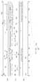
도 7a와 도 7b는 제 1 실시예와 제 2 실시예를 비교한 실험 데이터이다. 이때, 도 7a는 제 1 실시예, 도 7b는 제 2 실시예의 데이터 배선과 차폐 전극 간의 기생 커패시턴스의 용량과 화소의 충전 특성을 각각 나타낸 도면이다.7A and 7B are experimental data comparing the first embodiment and the second embodiment. 7A is a diagram showing the first embodiment, and FIG. 7B is a diagram showing the capacitance of the parasitic capacitance between the data line and the shielding electrode of the second embodiment and the charging characteristic of the pixel, respectively.
도 7a와 도 7b에 도시한 바와 같이, 제 1 실시예와 제 2 실시예에서 데이터 배선의 저항은 각각 25.3kΩ으로 변화가 없으나 데이터 배선과 차폐 전극 간의 기생 커패시턴스(Cdc)의 용량에 있어서, 제 1 실시예는 327.6pF, 제 2 실시예는 148.6pF으로 제 1 실시예 대비 제 2 실시예의 기생 커패시턴스(Cdc)의 용량이 64% 정도 감소하였다.As shown in Figs. 7A and 7B, the resistances of the data lines in the first and second embodiments are not changed to 25.3 k?, Respectively. However, in the capacitances of the parasitic capacitance Cdc between the data lines and the shield electrodes, The capacitance of the parasitic capacitance Cdc of the second embodiment is reduced by about 64% compared to the first embodiment, with 327.6 pF of the first embodiment and 148.6 pF of the second embodiment.
또한, 단위 화소의 충전 특성에서 제 1 실시예의 I 부분과 제 2 실시예의 H 부분을 비교한 결과, I 부분 대비 H 부분에서 데이터 신호의 파장이 우측 상단으로 올라간 것을 알 수 있다. 다시 말해, 제 1 실시예에서는 데이터 신호의 지연으로 충전 시간(12.08μs) 내에 화소의 충전이 완전히 이루어지지 않는 미충전 문제가 발생하였으나, 제 2 실시예에서는 충전 시간(12.08μs) 내에 화소의 충전이 이루어지는 것을 알 수 있다.As a result of comparing the I portion of the first embodiment with the H portion of the second embodiment in the charging characteristic of the unit pixel, it can be seen that the wavelength of the data signal rises to the right upper end in the H portion with respect to the I portion. In other words, in the first embodiment, an uncharged problem occurs in which the pixel is not fully charged within the charging time (12.08 μs) due to the delay of the data signal. In the second embodiment, however, As shown in FIG.
그러나, 본 발명은 상기 제 1 및 제 2 실시예에 한정되는 것은 아니며, 본 발명의 정신 및 사상을 벗어나지 않는 한도 내에서 다양하게 변형 및 변경할 수 있다는 것은 자명한 사실일 것이다.However, it should be understood that the present invention is not limited to the first and second embodiments, and various modifications and changes may be made without departing from the spirit and scope of the present invention.
도 1은 종래에 따른 횡전계 방식 액정표시장치용 어레이 기판을 나타낸 평면도.1 is a plan view showing a conventional array substrate for a transverse electric field type liquid crystal display device.
도 2는 도 1의 Ⅱ-Ⅱ'선을 따라 절단하여 나타낸 단면도.2 is a cross-sectional view taken along line II-II 'of FIG. 1;
도 3은 본 발명의 제 1 실시예에 따른 횡전계 방식 액정표시장치용 어레이 기판을 나타낸 평면도.3 is a plan view showing an array substrate for a liquid crystal display device of a transverse electric field system according to a first embodiment of the present invention.
도 4는 도 3의 Ⅳ-Ⅳ'선을 따라 절단하여 나타낸 단면도.4 is a cross-sectional view taken along line IV-IV 'of FIG. 3;
도 5는 본 발명의 제 2 실시예에 따른 횡전계 방식 액정표시장치용 어레이 기판을 나타낸 평면도.5 is a plan view showing an array substrate for a transverse electric field type liquid crystal display device according to a second embodiment of the present invention.
도 6은 도 5의 Ⅵ-Ⅵ'선을 따라 절단하여 나타낸 단면도.6 is a cross-sectional view taken along the line VI-VI 'of FIG. 5;
도 7a와 도 7b는 제 1 실시예와 제 2 실시예를 비교한 실험 데이터.7A and 7B are experimental data comparing the first embodiment and the second embodiment.
* 도면의 주요부분에 대한 부호의 설명*Description of the Related Art [0002]
210 : 기판 220 : 게이트 배선210: substrate 220: gate wiring
225a, 225b : 제 1 및 제 2 게이트 전극 230 : 데이터 배선225a, 225b: first and second gate electrodes 230: data wiring
232a : 제 1 소스 전극 232b : 제 2 소스 전극232a:
234a : 제 1 드레인 전극 234b : 제 2 드레인 전극234a:
240a : 제 1 액티브층 240b : 제 2 액티브층240a: first
250a : 제 1 공통 배선 250b : 제 2 공통 배선250a: first
270a : 제 1 화소 전극 270b : 제 2 화소 전극270a:
281 : 제 1 공통 전극 282 : 제 2 공통 전극281: first common electrode 282: second common electrode
283, 284, 285 : 제 1, 제 2, 제 3 차폐 전극283, 284, 285: first, second and third shielding electrodes
CH1, CH2 : 제 1 및 제 2 드레인 콘택홀CH1, CH2: first and second drain contact holes
T1, T2 : 제 1 및 제 2 박막트랜지스터T1, T2: first and second thin film transistors
Claims (10)
Translated fromKoreanPriority Applications (2)
| Application Number | Priority Date | Filing Date | Title |
|---|---|---|---|
| KR1020080016107AKR101439268B1 (en) | 2008-02-22 | 2008-02-22 | Array Substrate of In-Plane Switching Mode Liquid Crystal Display Device |
| US12/390,152US8330919B2 (en) | 2008-02-22 | 2009-02-20 | Array substrate for in-plane switching mode liquid crystal display device and method of fabricating the same |
Applications Claiming Priority (1)
| Application Number | Priority Date | Filing Date | Title |
|---|---|---|---|
| KR1020080016107AKR101439268B1 (en) | 2008-02-22 | 2008-02-22 | Array Substrate of In-Plane Switching Mode Liquid Crystal Display Device |
Publications (2)
| Publication Number | Publication Date |
|---|---|
| KR20090090708A KR20090090708A (en) | 2009-08-26 |
| KR101439268B1true KR101439268B1 (en) | 2014-09-12 |
Family
ID=41053224
Family Applications (1)
| Application Number | Title | Priority Date | Filing Date |
|---|---|---|---|
| KR1020080016107AActiveKR101439268B1 (en) | 2008-02-22 | 2008-02-22 | Array Substrate of In-Plane Switching Mode Liquid Crystal Display Device |
Country Status (2)
| Country | Link |
|---|---|
| US (1) | US8330919B2 (en) |
| KR (1) | KR101439268B1 (en) |
Families Citing this family (28)
| Publication number | Priority date | Publication date | Assignee | Title |
|---|---|---|---|---|
| KR101709346B1 (en)* | 2009-12-15 | 2017-03-08 | 엘지디스플레이 주식회사 | In plane switching mode Liquid crystal display device and Method of manufacturing the same |
| KR20120004045A (en)* | 2010-07-06 | 2012-01-12 | 삼성전자주식회사 | Liquid crystal display |
| KR101866388B1 (en)* | 2010-11-15 | 2018-06-12 | 엘지디스플레이 주식회사 | Thin film transistor substrate and method of fabricating the same |
| US10761358B2 (en) | 2011-03-03 | 2020-09-01 | Apple Inc. | Display screen shield line system |
| US20130342801A1 (en)* | 2011-03-03 | 2013-12-26 | Sharp Kabushiki Kaisha | Liquid crystal display device |
| CN104246593B (en)* | 2012-04-27 | 2016-11-23 | 夏普株式会社 | Liquid crystal display element and liquid crystal display device |
| JP5883721B2 (en)* | 2012-05-11 | 2016-03-15 | 株式会社ジャパンディスプレイ | Liquid crystal display |
| KR101396943B1 (en)* | 2012-06-25 | 2014-05-19 | 엘지디스플레이 주식회사 | Liquid crystal display device and manufacturing method |
| CN102998859B (en)* | 2012-12-14 | 2016-03-02 | 京东方科技集团股份有限公司 | A kind of array base palte and preparation method thereof and display device |
| CN104062814B (en)* | 2013-03-19 | 2016-08-10 | 北京京东方光电科技有限公司 | A pixel electrode layer, array substrate, display panel and display device |
| KR102053439B1 (en)* | 2013-08-20 | 2019-12-06 | 엘지디스플레이 주식회사 | In-plane switching mode liquid crystal display array substrate |
| CN103941488A (en)* | 2013-11-01 | 2014-07-23 | 上海中航光电子有限公司 | Fringe-field-switching-type liquid crystal display device, array substrate and manufacturing method of array substrate |
| KR102164311B1 (en)* | 2013-12-06 | 2020-10-13 | 삼성디스플레이 주식회사 | Liquid crystal display |
| KR102140815B1 (en) | 2013-12-09 | 2020-08-04 | 삼성디스플레이 주식회사 | Liquid crystal display |
| JP2015121583A (en)* | 2013-12-20 | 2015-07-02 | 株式会社ジャパンディスプレイ | LCD panel |
| KR20150109544A (en)* | 2014-03-19 | 2015-10-02 | 삼성디스플레이 주식회사 | Display device and manufacturing method thereof |
| CN105022184A (en)* | 2014-04-17 | 2015-11-04 | 株式会社日本显示器 | Display device |
| CN104216129B (en)* | 2014-09-12 | 2017-08-11 | 上海天马微电子有限公司 | Display panel and display device |
| CN104516167A (en)* | 2015-01-20 | 2015-04-15 | 京东方科技集团股份有限公司 | Array baseplate and display device |
| CN104965370B (en)* | 2015-07-31 | 2019-02-01 | 重庆京东方光电科技有限公司 | Array substrate and its manufacturing method, display device |
| CN105068340B (en) | 2015-09-21 | 2018-11-06 | 京东方科技集团股份有限公司 | Array substrate, display device and preparation method thereof |
| CN105446029A (en)* | 2016-01-19 | 2016-03-30 | 京东方科技集团股份有限公司 | Array substrate, liquid crystal display panel and display device |
| CN107967874B (en)* | 2016-10-19 | 2020-04-28 | 元太科技工业股份有限公司 | pixel structure |
| CN106652869B (en)* | 2016-11-07 | 2020-04-24 | 京东方科技集团股份有限公司 | Control circuit for display panel, driving method and display device |
| US11073734B2 (en)* | 2017-05-04 | 2021-07-27 | Chongqing Boe Optoelectronics Technology Co., Ltd. | Array substrate and method of manufacturing the same, display panel and display device |
| US10928691B2 (en)* | 2019-02-15 | 2021-02-23 | Sharp Kabushiki Kaisha | Active matrix substrate comprising a first contact hole that overlaps with a counter electrode control line and passes through a flattening film and liquid crystal display with the same |
| CN110888274B (en)* | 2019-11-27 | 2022-05-31 | 深圳市华星光电半导体显示技术有限公司 | Display panel |
| CN112162425B (en)* | 2020-10-29 | 2023-12-01 | 京东方科技集团股份有限公司 | Pixel unit, driving method thereof, array substrate and vertical alignment type display device |
Citations (2)
| Publication number | Priority date | Publication date | Assignee | Title |
|---|---|---|---|---|
| US6069678A (en) | 1996-10-29 | 2000-05-30 | Nec Corporation | Liquid crystal display device with data line electric field shield utilizing common electrode |
| US20080002126A1 (en) | 2006-06-30 | 2008-01-03 | Lg Philips Lcd Co., Ltd. | Thin film transistor substrate of horizontal electric field applying type and fabricating method thereof |
Family Cites Families (5)
| Publication number | Priority date | Publication date | Assignee | Title |
|---|---|---|---|---|
| JP2776376B2 (en)* | 1996-06-21 | 1998-07-16 | 日本電気株式会社 | Active matrix liquid crystal display panel |
| US5907379A (en)* | 1996-10-21 | 1999-05-25 | Samsung Electronics Co., Ltd. | In-plane switching liquid crystal display having high aperture ratio |
| US6133977A (en)* | 1997-10-21 | 2000-10-17 | Samsung Electronics Co., Ltd. | Liquid crystal displays having common electrode overlap with one or more data lines |
| JP3050191B2 (en)* | 1997-11-12 | 2000-06-12 | 日本電気株式会社 | Liquid crystal display |
| KR100881357B1 (en)* | 1999-09-07 | 2009-02-02 | 가부시키가이샤 히타치세이사쿠쇼 | LCD Display |
- 2008
- 2008-02-22KRKR1020080016107Apatent/KR101439268B1/enactiveActive
- 2009
- 2009-02-20USUS12/390,152patent/US8330919B2/enactiveActive
Patent Citations (2)
| Publication number | Priority date | Publication date | Assignee | Title |
|---|---|---|---|---|
| US6069678A (en) | 1996-10-29 | 2000-05-30 | Nec Corporation | Liquid crystal display device with data line electric field shield utilizing common electrode |
| US20080002126A1 (en) | 2006-06-30 | 2008-01-03 | Lg Philips Lcd Co., Ltd. | Thin film transistor substrate of horizontal electric field applying type and fabricating method thereof |
Also Published As
| Publication number | Publication date |
|---|---|
| US20090225250A1 (en) | 2009-09-10 |
| US8330919B2 (en) | 2012-12-11 |
| KR20090090708A (en) | 2009-08-26 |
Similar Documents
| Publication | Publication Date | Title |
|---|---|---|
| KR101439268B1 (en) | Array Substrate of In-Plane Switching Mode Liquid Crystal Display Device | |
| US11604392B2 (en) | Active matrix substrate and display panel | |
| KR102083433B1 (en) | Liquid crystal display | |
| KR101349092B1 (en) | Array substrate and display apparatus having the same | |
| KR101623160B1 (en) | Liquid crystal display | |
| KR100587217B1 (en) | Array board for liquid crystal display device of transverse electric field method and manufacturing method | |
| CN102156367B (en) | Array substrate, liquid crystal panel and liquid crystal displayer | |
| US9588380B2 (en) | Liquid crystal display device including an auxiliary capacitance line with a branch portion | |
| US9036121B2 (en) | Liquid crystal display panel and liquid crystal display device | |
| KR20150070776A (en) | Display apparatus | |
| KR100959367B1 (en) | Transverse electric field type liquid crystal display device | |
| KR100593314B1 (en) | Liquid crystal display | |
| KR20090054255A (en) | LCD Display | |
| KR102076841B1 (en) | Thin Film Transistor Substrate For Flat Panel Display Having Additional Common Line | |
| KR101310309B1 (en) | Display panel | |
| KR102053439B1 (en) | In-plane switching mode liquid crystal display array substrate | |
| KR100911420B1 (en) | Array board for transverse electric field type liquid crystal display device | |
| KR101245119B1 (en) | Array plate and display panel having the same | |
| KR20070014668A (en) | Transverse electric field type liquid crystal display device and manufacturing method thereof | |
| KR101308265B1 (en) | Liquid crystal display device | |
| US11169405B2 (en) | Display device comprising a first display electrode, a first electrode, and an insulating film including an inorganic insulating film and an organic insulating film | |
| KR20090072296A (en) | Array Board for Viewing Angle Control Liquid Crystal Display | |
| KR100816366B1 (en) | Transverse electric field liquid crystal display device | |
| KR100839834B1 (en) | Transverse electric field liquid crystal display device | |
| KR20120116575A (en) | In-plane switching mode liquid crystal display device |
Legal Events
| Date | Code | Title | Description |
|---|---|---|---|
| PA0109 | Patent application | St.27 status event code:A-0-1-A10-A12-nap-PA0109 | |
| PN2301 | Change of applicant | St.27 status event code:A-3-3-R10-R13-asn-PN2301 St.27 status event code:A-3-3-R10-R11-asn-PN2301 | |
| P11-X000 | Amendment of application requested | St.27 status event code:A-2-2-P10-P11-nap-X000 | |
| P13-X000 | Application amended | St.27 status event code:A-2-2-P10-P13-nap-X000 | |
| R15-X000 | Change to inventor requested | St.27 status event code:A-3-3-R10-R15-oth-X000 | |
| R16-X000 | Change to inventor recorded | St.27 status event code:A-3-3-R10-R16-oth-X000 | |
| PG1501 | Laying open of application | St.27 status event code:A-1-1-Q10-Q12-nap-PG1501 | |
| R18-X000 | Changes to party contact information recorded | St.27 status event code:A-3-3-R10-R18-oth-X000 | |
| R18-X000 | Changes to party contact information recorded | St.27 status event code:A-3-3-R10-R18-oth-X000 | |
| R18-X000 | Changes to party contact information recorded | St.27 status event code:A-3-3-R10-R18-oth-X000 | |
| A201 | Request for examination | ||
| PA0201 | Request for examination | St.27 status event code:A-1-2-D10-D11-exm-PA0201 | |
| P11-X000 | Amendment of application requested | St.27 status event code:A-2-2-P10-P11-nap-X000 | |
| P13-X000 | Application amended | St.27 status event code:A-2-2-P10-P13-nap-X000 | |
| E902 | Notification of reason for refusal | ||
| PE0902 | Notice of grounds for rejection | St.27 status event code:A-1-2-D10-D21-exm-PE0902 | |
| P11-X000 | Amendment of application requested | St.27 status event code:A-2-2-P10-P11-nap-X000 | |
| P13-X000 | Application amended | St.27 status event code:A-2-2-P10-P13-nap-X000 | |
| E701 | Decision to grant or registration of patent right | ||
| PE0701 | Decision of registration | St.27 status event code:A-1-2-D10-D22-exm-PE0701 | |
| GRNT | Written decision to grant | ||
| PR0701 | Registration of establishment | St.27 status event code:A-2-4-F10-F11-exm-PR0701 | |
| PR1002 | Payment of registration fee | St.27 status event code:A-2-2-U10-U11-oth-PR1002 Fee payment year number:1 | |
| PG1601 | Publication of registration | St.27 status event code:A-4-4-Q10-Q13-nap-PG1601 | |
| FPAY | Annual fee payment | Payment date:20170816 Year of fee payment:4 | |
| PR1001 | Payment of annual fee | St.27 status event code:A-4-4-U10-U11-oth-PR1001 Fee payment year number:4 | |
| FPAY | Annual fee payment | Payment date:20180816 Year of fee payment:5 | |
| PR1001 | Payment of annual fee | St.27 status event code:A-4-4-U10-U11-oth-PR1001 Fee payment year number:5 | |
| PR1001 | Payment of annual fee | St.27 status event code:A-4-4-U10-U11-oth-PR1001 Fee payment year number:6 | |
| PR1001 | Payment of annual fee | St.27 status event code:A-4-4-U10-U11-oth-PR1001 Fee payment year number:7 | |
| PR1001 | Payment of annual fee | St.27 status event code:A-4-4-U10-U11-oth-PR1001 Fee payment year number:8 | |
| PR1001 | Payment of annual fee | St.27 status event code:A-4-4-U10-U11-oth-PR1001 Fee payment year number:9 | |
| PR1001 | Payment of annual fee | St.27 status event code:A-4-4-U10-U11-oth-PR1001 Fee payment year number:10 | |
| PR1001 | Payment of annual fee | St.27 status event code:A-4-4-U10-U11-oth-PR1001 Fee payment year number:11 | |
| PR1001 | Payment of annual fee | St.27 status event code:A-4-4-U10-U11-oth-PR1001 Fee payment year number:12 |