KR101438647B1 - Container member and flat display apparatus having the same - Google Patents
Container member and flat display apparatus having the sameDownload PDFInfo
- Publication number
- KR101438647B1 KR101438647B1KR1020080004406AKR20080004406AKR101438647B1KR 101438647 B1KR101438647 B1KR 101438647B1KR 1020080004406 AKR1020080004406 AKR 1020080004406AKR 20080004406 AKR20080004406 AKR 20080004406AKR 101438647 B1KR101438647 B1KR 101438647B1
- Authority
- KR
- South Korea
- Prior art keywords
- grounding
- body portion
- insulating body
- bottom plate
- metal
- Prior art date
- Legal status (The legal status is an assumption and is not a legal conclusion. Google has not performed a legal analysis and makes no representation as to the accuracy of the status listed.)
- Expired - Fee Related
Links
Images


Classifications
- H—ELECTRICITY
- H05—ELECTRIC TECHNIQUES NOT OTHERWISE PROVIDED FOR
- H05K—PRINTED CIRCUITS; CASINGS OR CONSTRUCTIONAL DETAILS OF ELECTRIC APPARATUS; MANUFACTURE OF ASSEMBLAGES OF ELECTRICAL COMPONENTS
- H05K7/00—Constructional details common to different types of electric apparatus
- H05K7/20—Modifications to facilitate cooling, ventilating, or heating
- H05K7/20954—Modifications to facilitate cooling, ventilating, or heating for display panels
- H05K7/20963—Heat transfer by conduction from internal heat source to heat radiating structure
- G—PHYSICS
- G02—OPTICS
- G02F—OPTICAL DEVICES OR ARRANGEMENTS FOR THE CONTROL OF LIGHT BY MODIFICATION OF THE OPTICAL PROPERTIES OF THE MEDIA OF THE ELEMENTS INVOLVED THEREIN; NON-LINEAR OPTICS; FREQUENCY-CHANGING OF LIGHT; OPTICAL LOGIC ELEMENTS; OPTICAL ANALOGUE/DIGITAL CONVERTERS
- G02F1/00—Devices or arrangements for the control of the intensity, colour, phase, polarisation or direction of light arriving from an independent light source, e.g. switching, gating or modulating; Non-linear optics
- G02F1/01—Devices or arrangements for the control of the intensity, colour, phase, polarisation or direction of light arriving from an independent light source, e.g. switching, gating or modulating; Non-linear optics for the control of the intensity, phase, polarisation or colour
- G02F1/13—Devices or arrangements for the control of the intensity, colour, phase, polarisation or direction of light arriving from an independent light source, e.g. switching, gating or modulating; Non-linear optics for the control of the intensity, phase, polarisation or colour based on liquid crystals, e.g. single liquid crystal display cells
- G02F1/133—Constructional arrangements; Operation of liquid crystal cells; Circuit arrangements
- G02F1/1333—Constructional arrangements; Manufacturing methods
- H—ELECTRICITY
- H05—ELECTRIC TECHNIQUES NOT OTHERWISE PROVIDED FOR
- H05K—PRINTED CIRCUITS; CASINGS OR CONSTRUCTIONAL DETAILS OF ELECTRIC APPARATUS; MANUFACTURE OF ASSEMBLAGES OF ELECTRICAL COMPONENTS
- H05K9/00—Screening of apparatus or components against electric or magnetic fields
- H05K9/0007—Casings
- H05K9/0054—Casings specially adapted for display applications
- G—PHYSICS
- G02—OPTICS
- G02F—OPTICAL DEVICES OR ARRANGEMENTS FOR THE CONTROL OF LIGHT BY MODIFICATION OF THE OPTICAL PROPERTIES OF THE MEDIA OF THE ELEMENTS INVOLVED THEREIN; NON-LINEAR OPTICS; FREQUENCY-CHANGING OF LIGHT; OPTICAL LOGIC ELEMENTS; OPTICAL ANALOGUE/DIGITAL CONVERTERS
- G02F1/00—Devices or arrangements for the control of the intensity, colour, phase, polarisation or direction of light arriving from an independent light source, e.g. switching, gating or modulating; Non-linear optics
- G02F1/01—Devices or arrangements for the control of the intensity, colour, phase, polarisation or direction of light arriving from an independent light source, e.g. switching, gating or modulating; Non-linear optics for the control of the intensity, phase, polarisation or colour
- G02F1/13—Devices or arrangements for the control of the intensity, colour, phase, polarisation or direction of light arriving from an independent light source, e.g. switching, gating or modulating; Non-linear optics for the control of the intensity, phase, polarisation or colour based on liquid crystals, e.g. single liquid crystal display cells
- G02F1/133—Constructional arrangements; Operation of liquid crystal cells; Circuit arrangements
- G02F1/1333—Constructional arrangements; Manufacturing methods
- G02F1/133308—Support structures for LCD panels, e.g. frames or bezels
- G02F1/133314—Back frames
- G—PHYSICS
- G02—OPTICS
- G02F—OPTICAL DEVICES OR ARRANGEMENTS FOR THE CONTROL OF LIGHT BY MODIFICATION OF THE OPTICAL PROPERTIES OF THE MEDIA OF THE ELEMENTS INVOLVED THEREIN; NON-LINEAR OPTICS; FREQUENCY-CHANGING OF LIGHT; OPTICAL LOGIC ELEMENTS; OPTICAL ANALOGUE/DIGITAL CONVERTERS
- G02F1/00—Devices or arrangements for the control of the intensity, colour, phase, polarisation or direction of light arriving from an independent light source, e.g. switching, gating or modulating; Non-linear optics
- G02F1/01—Devices or arrangements for the control of the intensity, colour, phase, polarisation or direction of light arriving from an independent light source, e.g. switching, gating or modulating; Non-linear optics for the control of the intensity, phase, polarisation or colour
- G02F1/13—Devices or arrangements for the control of the intensity, colour, phase, polarisation or direction of light arriving from an independent light source, e.g. switching, gating or modulating; Non-linear optics for the control of the intensity, phase, polarisation or colour based on liquid crystals, e.g. single liquid crystal display cells
- G02F1/133—Constructional arrangements; Operation of liquid crystal cells; Circuit arrangements
- G02F1/1333—Constructional arrangements; Manufacturing methods
- G02F1/133308—Support structures for LCD panels, e.g. frames or bezels
- G02F1/133322—Mechanical guidance or alignment of LCD panel support components
- G—PHYSICS
- G02—OPTICS
- G02F—OPTICAL DEVICES OR ARRANGEMENTS FOR THE CONTROL OF LIGHT BY MODIFICATION OF THE OPTICAL PROPERTIES OF THE MEDIA OF THE ELEMENTS INVOLVED THEREIN; NON-LINEAR OPTICS; FREQUENCY-CHANGING OF LIGHT; OPTICAL LOGIC ELEMENTS; OPTICAL ANALOGUE/DIGITAL CONVERTERS
- G02F1/00—Devices or arrangements for the control of the intensity, colour, phase, polarisation or direction of light arriving from an independent light source, e.g. switching, gating or modulating; Non-linear optics
- G02F1/01—Devices or arrangements for the control of the intensity, colour, phase, polarisation or direction of light arriving from an independent light source, e.g. switching, gating or modulating; Non-linear optics for the control of the intensity, phase, polarisation or colour
- G02F1/13—Devices or arrangements for the control of the intensity, colour, phase, polarisation or direction of light arriving from an independent light source, e.g. switching, gating or modulating; Non-linear optics for the control of the intensity, phase, polarisation or colour based on liquid crystals, e.g. single liquid crystal display cells
- G02F1/133—Constructional arrangements; Operation of liquid crystal cells; Circuit arrangements
- G02F1/1333—Constructional arrangements; Manufacturing methods
- G02F1/1335—Structural association of cells with optical devices, e.g. polarisers or reflectors
- G02F1/1336—Illuminating devices
- G02F1/133602—Direct backlight
- G02F1/133608—Direct backlight including particular frames or supporting means
- G—PHYSICS
- G02—OPTICS
- G02F—OPTICAL DEVICES OR ARRANGEMENTS FOR THE CONTROL OF LIGHT BY MODIFICATION OF THE OPTICAL PROPERTIES OF THE MEDIA OF THE ELEMENTS INVOLVED THEREIN; NON-LINEAR OPTICS; FREQUENCY-CHANGING OF LIGHT; OPTICAL LOGIC ELEMENTS; OPTICAL ANALOGUE/DIGITAL CONVERTERS
- G02F1/00—Devices or arrangements for the control of the intensity, colour, phase, polarisation or direction of light arriving from an independent light source, e.g. switching, gating or modulating; Non-linear optics
- G02F1/01—Devices or arrangements for the control of the intensity, colour, phase, polarisation or direction of light arriving from an independent light source, e.g. switching, gating or modulating; Non-linear optics for the control of the intensity, phase, polarisation or colour
- G02F1/13—Devices or arrangements for the control of the intensity, colour, phase, polarisation or direction of light arriving from an independent light source, e.g. switching, gating or modulating; Non-linear optics for the control of the intensity, phase, polarisation or colour based on liquid crystals, e.g. single liquid crystal display cells
- G02F1/133—Constructional arrangements; Operation of liquid crystal cells; Circuit arrangements
- G02F1/1333—Constructional arrangements; Manufacturing methods
- G02F1/1335—Structural association of cells with optical devices, e.g. polarisers or reflectors
- G02F1/1336—Illuminating devices
- G02F1/133628—Illuminating devices with cooling means
- G—PHYSICS
- G02—OPTICS
- G02F—OPTICAL DEVICES OR ARRANGEMENTS FOR THE CONTROL OF LIGHT BY MODIFICATION OF THE OPTICAL PROPERTIES OF THE MEDIA OF THE ELEMENTS INVOLVED THEREIN; NON-LINEAR OPTICS; FREQUENCY-CHANGING OF LIGHT; OPTICAL LOGIC ELEMENTS; OPTICAL ANALOGUE/DIGITAL CONVERTERS
- G02F1/00—Devices or arrangements for the control of the intensity, colour, phase, polarisation or direction of light arriving from an independent light source, e.g. switching, gating or modulating; Non-linear optics
- G02F1/01—Devices or arrangements for the control of the intensity, colour, phase, polarisation or direction of light arriving from an independent light source, e.g. switching, gating or modulating; Non-linear optics for the control of the intensity, phase, polarisation or colour
- G02F1/13—Devices or arrangements for the control of the intensity, colour, phase, polarisation or direction of light arriving from an independent light source, e.g. switching, gating or modulating; Non-linear optics for the control of the intensity, phase, polarisation or colour based on liquid crystals, e.g. single liquid crystal display cells
- G02F1/133—Constructional arrangements; Operation of liquid crystal cells; Circuit arrangements
- G02F1/1333—Constructional arrangements; Manufacturing methods
- G02F1/1345—Conductors connecting electrodes to cell terminals
- G02F1/13452—Conductors connecting driver circuitry and terminals of panels
- G—PHYSICS
- G02—OPTICS
- G02F—OPTICAL DEVICES OR ARRANGEMENTS FOR THE CONTROL OF LIGHT BY MODIFICATION OF THE OPTICAL PROPERTIES OF THE MEDIA OF THE ELEMENTS INVOLVED THEREIN; NON-LINEAR OPTICS; FREQUENCY-CHANGING OF LIGHT; OPTICAL LOGIC ELEMENTS; OPTICAL ANALOGUE/DIGITAL CONVERTERS
- G02F2201/00—Constructional arrangements not provided for in groups G02F1/00 - G02F7/00
- G02F2201/50—Protective arrangements
- G02F2201/503—Arrangements improving the resistance to shock
- Y—GENERAL TAGGING OF NEW TECHNOLOGICAL DEVELOPMENTS; GENERAL TAGGING OF CROSS-SECTIONAL TECHNOLOGIES SPANNING OVER SEVERAL SECTIONS OF THE IPC; TECHNICAL SUBJECTS COVERED BY FORMER USPC CROSS-REFERENCE ART COLLECTIONS [XRACs] AND DIGESTS
- Y10—TECHNICAL SUBJECTS COVERED BY FORMER USPC
- Y10T—TECHNICAL SUBJECTS COVERED BY FORMER US CLASSIFICATION
- Y10T29/00—Metal working
- Y10T29/49—Method of mechanical manufacture
- Y10T29/49002—Electrical device making
Landscapes
- Physics & Mathematics (AREA)
- Engineering & Computer Science (AREA)
- Microelectronics & Electronic Packaging (AREA)
- Nonlinear Science (AREA)
- Thermal Sciences (AREA)
- Mathematical Physics (AREA)
- Chemical & Material Sciences (AREA)
- Crystallography & Structural Chemistry (AREA)
- General Physics & Mathematics (AREA)
- Optics & Photonics (AREA)
- Liquid Crystal (AREA)
- Devices For Indicating Variable Information By Combining Individual Elements (AREA)
Abstract
Translated fromKoreanDescription
Translated fromKorean본 발명은 수납 부재 및 이를 구비한 표시 장치에 관한 것으로, 무게가 가벼운 절연성 재질과 금속 재질을 복합 적용하여 제작된 수납 부재에 관한 것이다.BACKGROUND OF THE
평판 표시 장치는 평판 형의 표시 패널과 패널을 수납하는 수납 부재를 구비한다. 수납 부재는 표시 패널을 그 내측에 수납하여, 표시 패널을 고정시킬 뿐만 아니라 외부 충격으로부터 표시 패널을 보호하였다.The flat panel display includes a flat display panel and a housing member for housing the panel. The housing member accommodates the display panel inside thereof, thereby not only fixing the display panel but also protecting the display panel from an external impact.
표시 패널의 사이즈가 증대됨에 따라 이를 수납하는 수납 부재의 사이즈 또한 증가하게 되었다. 종래에는 수납 부재를 알루미늄과 같은 금속 재질로 제작하여 사용하였다. 이경우 수납 부재의 사이즈가 증대됨에 따라 수납 부재의 무게가 증가하게 되는 문제가 발생하였다. 또한, 표시 패널로 액정 표시 패널을 사용하는 경우, 수납 부재의 바닥판 내측표면 영역에 복수의 램프를 배치하여 백라이트로 사용한다. 이때, 금속의 수납 부재와 램프 사이에 기생 캡이 발생하여 누설 전류가 증 가하게 된다. 이는 복수 램프의 특성(램프들 간의 균일도)을 저하시키는 원인이 된다. 또한, 금속의 수납 부재는 램프의 열을 차단하지 못하고, 수납 부재의 바닥판 외측표면에 부착된 컨트롤 보드에 그대로 전달한다. 이로인해 컨트롤 보드의 온도가 상승되어 컨트롤 보드가 오동작하는 원인이 된다.As the size of the display panel increases, the size of the housing member for accommodating the display panel also increases. Conventionally, the housing member is made of a metal material such as aluminum. In this case, as the size of the storage member increases, a problem arises that the weight of the storage member increases. When a liquid crystal display panel is used as the display panel, a plurality of lamps are arranged in the inner surface area of the bottom plate of the housing member to be used as a backlight. At this time, a parasitic cap is generated between the metal receiving member and the lamp, thereby increasing the leakage current. This causes degradation of the characteristics of the plurality of lamps (uniformity between the lamps). In addition, the metal receiving member does not interrupt the heat of the lamp, and the metal receiving member transfers the same to the control board attached to the outer surface of the bottom plate of the receiving member. This causes the temperature of the control board to rise, causing the control board to malfunction.
이에 본 발명은 무게를 줄일 수 있고, 램프 특성을 향상시키며, 수납 부재 외측으로 발산되는 열을 줄이기 위해 내측에 접지 금속부가 마련된 절연성 합성 수지를 이용하여 제작된 수납 부재 및 이를 구비한 표시 장치를 제공한다.Accordingly, the present invention provides a storage member made of an insulating synthetic resin having a ground metal portion on the inner side to reduce the weight, improve the lamp characteristics, and dissipate heat to the outside of the storage member, and a display device having the same do.
본 발명에 따른 화상을 표시하는 표시 패널을 수납하는 수납 부재에 있어서, 바닥판과 측벽을 구비하여 수납 공간을 형성하는 절연성 몸체부 및 상기 절연성 몸체부의 일부 영역에 마련되고, 상기 절연성 몸체부와 일체로 제작된 적어도 하나의 접지 금속부를 포함하는 수납 부재를 제공한다.There is provided a housing member for housing a display panel for displaying an image according to the present invention, the housing member comprising: an insulating body portion having a bottom plate and side walls to form a storage space; and an insulating body portion provided in a part of the insulating body portion, And at least one ground metal portion made of a metal material.
상기 절연성 몸체부는 절연성 합성 수지로 제작되는 것이 효과적이다.It is effective that the insulating body portion is made of an insulating synthetic resin.
상기 합성 수지로 폴리카보네이트(Polycarbonate; PC), 폴리에틸렌테레프탈레이트(polyethyleneterephthalate; PET), 폴리에틸렌(polyethylene; PE), 폴리프로필렌(polypropylene; PP), 폴리스틸렌(polystyrene; PS), ABS(Acrylonitrile-Butadiene-Styrene) 및 스티렌 아크릴로니트릴 코폴리머(Styrene Acrylonitrile Copolymers; SAN) 중 어느 하나를 사용하는 것이 가능하다.(PET), polyethylene (PE), polypropylene (PP), polystyrene (PS), ABS (acrylonitrile-butadiene-styrene ) And styrene acrylonitrile copolymers (SAN) can be used.
상기 접지 금속부는 접지 금속 판과 접촉 패드를 구비하는 것이 바람직하다.Preferably, the grounded metal portion comprises a grounded metal plate and a contact pad.
상기 접지 금속 판은 상기 바닥판 내에 매설되거나, 상기 바닥판의 외측 표면 또는 내측 표면 중 하나에 위치하는 것이 효과적이다.It is effective that the grounding metal plate is embedded in the bottom plate or located on one of the outer surface or the inner surface of the bottom plate.
상기 바닥판에 오목홈이 형성되고, 상기 오목홈 내에 상기 접지 금속 판이 마련되거나, 상기 바닥판에 관통홀이 형성되고, 상기 관통홀 내에 상기 접지 금속 판이 마련될 수도 있다.A ground metal plate may be provided in the concave groove in the bottom plate, a through hole may be formed in the bottom plate, and the grounding metal plate may be provided in the through hole.
상기 접촉 패드는 상기 접지 금속 판에서 돌출된 접지 돌기를 포함하는 것이 바람직하다.The contact pad preferably includes a grounding protrusion protruding from the grounding metal plate.
상기 접지 돌기는 상기 접지 금속 판의 일부를 절곡시켜 제작되는 것이 효과적이다.It is effective that the grounding projection is formed by bending a part of the grounding metal plate.
상기 접지 금속 판은 상기 바닥판 내에 매설되고, 상기 접촉 패드는 상기 접지 금속 판의 일부를 노출시키는 노출홈을 구비하는 것이 효과적이다.It is effective that the grounding metal plate is embedded in the bottom plate, and the contact pad has an exposure groove exposing a part of the grounding metal plate.
상기 접촉 패드는 상기 노출홈을 매립하는 도전성 물질을 더 구비하는 것이 바람직하다.The contact pad may further include a conductive material filling the exposed groove.
상기 접지 금속부는 상기 바닥판의 외측 표면에 판 또는 박막 형태로 제작되고, 상기 접지 금속부가 형성된 상기 바닥판의 일부 영역이 돌기 형태로 돌출되고, 상기 박막 형태의 접지 금속부는 금속 인쇄 방법으로 제작하거나, 금속 박막을 상기 바닥판의 외측 표면에 부착시켜 제작되는 것이 가능하다.The ground metal part is formed in the form of a plate or a thin film on the outer surface of the bottom plate, a part of the bottom plate on which the ground metal part is formed is protruded in a protrusion form, , And attaching a metal thin film to the outer surface of the bottom plate.
또한, 본 발명에 따른 바닥판과 측벽을 구비하여 수납 공간을 형성하는 절연성 몸체부와, 상기 절연성 몸체부의 일부 영역에 위치하고, 상기 절연성 몸체부와 일체로 제작된 적어도 하나의 접지 금속부를 포함하는 수납 부재와, 상기 수납 부재의 수납 공간 내에 수납된 램프 유닛 및 상기 램프 유닛 상에 마련된 표시 패널을 구비하는 표시 장치를 제공한다.In addition, the present invention provides an electronic apparatus comprising: an insulating body portion having a bottom plate and side walls according to the present invention to form a storage space; and at least one grounding metal portion located in a part of the insulating body portion, And a display panel provided on the lamp unit and a display panel accommodated in the storage space of the storing member.
상기 바닥판의 외측 표면에 각기 마련되어 상기 표시 패널에 화상 표시를 위한 제어 신호를 제공하는 컨트롤 보드와, 상기 램프 유닛에 전원을 제공하는 램프 전원 공급부를 더 구비하고, 상기 컨트롤 보드 및 상기 램프 전원 공급부의 접지부가 상기 접지 금속부에 접속되는 것이 효과적이다.A control board provided on the outer surface of the bottom plate for providing a control signal for displaying an image on the display panel and a lamp power supply unit for supplying power to the lamp unit, Is connected to the grounding metal portion.
상기 접지 금속부는 상기 컨트롤 보드의 접지부에 접속된 제 1 접지 금속부와, 상기 램프 전원 공급부의 접지부에 접속된 제 2 접지 금속부를 구비하고, 상기 제 1 및 제 2 접지 금속부는 이격되는 것이 바람직하다.Wherein the ground metal portion includes a first ground metal portion connected to a ground portion of the control board and a second ground metal portion connected to a ground portion of the lamp power supply portion and the first and second ground metal portions are spaced apart from each other desirable.
상기 컨트롤 보드에 영상 신호를 제공하는 세트 박스를 더 구비하고, 상기 접지 금속부는 상기 세트 박스가 접속된 제 3 접지 금속부를 더 구비하며, 적어도 상기 제 1 및 제 3 접지 금속부는 전기적으로 연결되고, 상기 제 1 내지 제 3 접지 금속부 각각이 복수의 영역으로 분리되는 것이 효과적이다.Further comprising a set box for providing an image signal to the control board, wherein the ground metal portion further comprises a third ground metal portion to which the set box is connected, at least the first and third ground metal portions are electrically connected, It is effective that each of the first to third ground metal portions is divided into a plurality of regions.
상기 접지 금속부는 상기 바닥판 내측 및 외측 표면에 판 또는 박막 형태로 마련되고, 상기 컨트롤 보드, 상기 램프 전원 공급부 및 상기 세트 박스의 접지부에 접속된 접지 돌기를 구비하는 것이 바람직하다.Preferably, the grounding metal part is provided on the inner and outer surfaces of the bottom plate in the form of a plate or a thin film, and includes grounding protrusions connected to the control board, the lamp power supply part, and the grounding part of the set box.
상기 접지 돌기와 상기 접지부는 나사, 후크, 볼트 및 도전성 접착제를 포함하는 결합부재에 의해 결합되는 것이 가능하다.The grounding projection and the grounding portion can be joined by a coupling member including a screw, a hook, a bolt, and a conductive adhesive.
상기 절연성 몸체부의 바닥판 내측 표면에 상기 램프 유닛을 지지하는 램프 홀더 및 램프 서포터가 상기 몸체부와 일체로 제작되는 것이 효과적이다.It is effective that the lamp holder and the lamp supporter supporting the lamp unit are integrally formed with the body part on the inner surface of the bottom plate of the insulating body part.
상기 바닥판의 외측 표면에 각기 마련되어 상기 표시 패널에 화상 표시를 위한 제어 신호를 제공하는 컨트롤 보드와, 상기 램프 유닛에 전원을 제공하는 램프 전원 공급부를 더 구비하고, 상기 바닥판 외측에 상기 컨트롤 보드 및 상기 램프 전원 공급부를 고정하는 고정부재가 상기 몸체부와 일체로 제작될 수 있다.A control board provided on the outer surface of the bottom plate for providing a control signal for displaying an image on the display panel and a lamp power supply unit for supplying power to the lamp unit, And a fixing member for fixing the lamp power supply unit may be integrally formed with the body.
또한, 본 발명에 따른 화상을 표시하는 표시 패널을 수납하는 수납 부재의 제조 방법에 있어서, 적어도 하나의 접지 돌기가 형성된 접지 금속판을 준비하는 단계와, 몸체부 제작을 위한 금형 내에 적어도 하나의 상기 접지 금속판을 배치시키는 단계 및 합성 수지의 사출을 통해 그 내부에 상기 접지 금속판이 매설되고, 상기 접지 돌기가 외부로 돌출되고, 수납 공간을 갖는 몸체부를 제작하는 단계를 포함하는 수납 부재의 제조 방법을 제공한다.In addition, in the method of manufacturing the housing member for housing the display panel for displaying an image according to the present invention, a step of preparing a grounding metal plate on which at least one grounding projection is formed, A step of disposing a metal plate and a step of forming a body portion having the grounding metal plate embedded therein through the injection of a synthetic resin and the grounding projection projecting to the outside and having a storage space; do.
상술한 바와 같이, 본 발명은 수납 부재를 절연성 합성 수지로 제작하여, 수납 부재의 무게를 줄일 수 있고, 수납 부재 내부 열이 상기 제어 요소에 전달되어 제어 요소를 열화시키는 현상을 방지할 수 있다.INDUSTRIAL APPLICABILITY As described above, the present invention can reduce the weight of the housing member by making the housing member made of an insulating synthetic resin, and prevent the internal heat of the housing member from being transmitted to the control element and deteriorating the control element.
또한, 본 발명은 수납 부재에 고정되는 컨트롤 보드와 같은 제어 요소들에 대응하는 수납 부재 영역에 국부적으로 접지 금속부를 형성하여 제어 요소들의 EMI 및 ESD 성능을 향상시킬 수 있다.Further, the present invention can improve the EMI and ESD performance of the control elements by forming a ground metal part locally in the receiving member area corresponding to the control elements such as the control board fixed to the receiving member.
또한, 본 발명은 수납 부재를 절연성 물질로 제작하여 수납 부재와 램프 사이의 기생 커패시터 발생을 방지하여 램프의 누설 전류 발생을 차단할 수 있고, 이를 통해 복수 램프들 간의 휘도 균일도를 향상시킬 수 있다.In addition, according to the present invention, it is possible to prevent the generation of parasitic capacitors between the storage member and the lamp by making the storage member made of an insulating material, thereby preventing the leakage current of the lamp from being generated, thereby improving the luminance uniformity among the plurality of lamps.
첨부된 도면을 참조하여 본 발명의 실시예를 더욱 상세히 설명한다. 그러나 본 발명은 이하에서 개시되는 실시예에 한정되는 것이 아니라 서로 다른 다양한 형태로 구현될 것이며, 단지 본 실시예들은 본 발명의 개시가 완전하도록 하며, 통상의 지식을 가진 자에게 발명의 범주를 완전하게 알려주기 위해 제공되는 것이다.Embodiments of the present invention will now be described in more detail with reference to the accompanying drawings. It will be apparent to those skilled in the art that the present invention may be embodied in many different forms and should not be construed as limited to the embodiments set forth herein. Rather, these embodiments are provided so that this disclosure will be thorough and complete, It is provided to let you know.
도 1은 본 발명의 일 실시예에 따른 표시 장치의 분해 사시도이고, 도 2는 일 실시예에 따른 표시 장치의 조립 단면도이다. 도 3은 일 실시예에 따른 하부 수납 부재와 이에 고정되는 요소들을 설명하기 위한 분해 사시도이고, 도 4는 일 실시예에 따른 하부 수납 부재의 단면도이고, 도 5는 일 실시예에 따른 하부 수납 부재에 일 요소가 접속된 단면도이다. 도 6 및 도 7은 일 실시예의 변형예에 따른 하부 수납 부재의 평면도이다. 도 8 내지 16은 일 실시예의 변형예에 따른 하부 수납 부재의 단면도이다.FIG. 1 is an exploded perspective view of a display device according to an embodiment of the present invention, and FIG. 2 is an assembled cross-sectional view of a display device according to an embodiment. FIG. 3 is an exploded perspective view illustrating a lower housing member according to an embodiment and elements fixed to the lower housing member. FIG. 4 is a sectional view of a lower housing member according to an embodiment, And Fig. 6 and 7 are plan views of a lower housing member according to a modification of the embodiment. 8 to 16 are sectional views of a lower housing member according to a modification of the embodiment.
도 1 내지 도 5를 참조하면, 본 실시예에 따른 표시 장치는 디스플레이 어셈블리(10)와 백라이트 어셈블리(20)를 포함한다.Referring to Figs. 1 to 5, a display device according to the present embodiment includes a
디스플레이 어셈블리(10)는 액정 표시 패널(100)과, 컨트롤 보드(200)와, 패널 지지 부재(300)와, 상부 수납 부재(400)를 포함한다.The
액정 표시 패널(100)은 컬러 필터와 공통 전극이 형성된 상부 기판(110)과, 박막 트랜지스터(thin firm transistor; TFT)와 화소 전극이 형성된 하부 기판(120)을 구비한다. 그리고, 상부 기판(110)과 하부 기판(120) 사이에는 액정층이 마련된다.The liquid
상부 기판(110) 상에는 차광 패턴과, 광이 통과하면서 소정의 색이 발현되는 색화소인 R, G, B 컬러 필터가 형성된다. 차광 패턴과 컬러 필터 상에는 인듐 틴 옥사이드(indium tin oxide: ITO) 또는 인듐 징크 옥사이드(indium zinc oxide: IZO) 등의 투명한 도전체로 이루어진 공통 전극이 위치한다. 필요에 따라 상기 차광 패턴과 컬러 필터가 하부 기판(120) 상에 형성될 수도 있다.On the
하부 기판(120)은 매트릭스 형태로 배치된 복수의 화소 전극과 복수의 화소 전극에 각기 접속된 박막 트랜지스터를 구비한다. 그리고, 박막 트랜지스터의 소스 단자에는 데이터 라인이 연결되며, 게이트 단자에는 게이트 라인이 연결된다.The
게이트 라인에 턴온 전압을 인가하면 게이트 라인에 접속된 박막 트랜지스터들이 턴온된다. 이때, 데이터 라인을 통해 화상 신호를 인가하게 되면 턴온된 박막 트랜지스터에 의해 데이터 라인의 화상 신호가 화소 전극에 차징 된다. 이로인해 하부 기판(120)의 화소 전극과 상부 기판(110)의 공통 전극 사이에는 전계가 형성된다. 따라서, 상기 전계에 의해 두 기판 사이에 마련된 액정의 배열이 변화된다. 액정은 그 배열의 변화에 따라 광투과율이 변경된다. 이를 통해 원하는 화상을 얻게 된다.When a turn-on voltage is applied to the gate line, the thin film transistors connected to the gate line are turned on. At this time, when an image signal is applied through the data line, the image signal of the data line is charged to the pixel electrode by the turned-on thin film transistor. Thus, an electric field is formed between the pixel electrode of the
도 2에 도시된 바와 같이 상부 기판(110)의 상측면과 하부 기판(120)의 후면에는 편광시트(130)가 부착되는 것이 바람직하다.As shown in FIG. 2, the polarizing
컨트롤 보드(200)는 화상 표현을 위한 다양한 신호들을 액정 표시 패널(200)에 제공한다. 도 1에서는 연성 인쇄 회로 기판(201)을 통해 컨트롤 보드(200)가 하부 기판(120)에 전기적으로 접속됨이 도시되었다. 컨트롤 보드(200)에는 액정 표시 패널(200) 구동을 위한 다양한 요소들이 실장된다. 이러한 요소로는 내부 전압 생성을 위한 전압 생성부와, 계조 전압을 생성하는 계조 전압 생성부와, 화상 신호를 데이터 라인에 제공하기 위한 데이터 구동부와, 턴온 전압을 게이트 라인에 제공하기 위한 게이트 구동부 그리고, 전압 생성부, 계조 전압 생성부, 데이터 구동부 및 게이트 구동부의 동작을 제어하는 제어부를 포함할 수 있다. 또한, 컨트롤 보드(200)에는 외부 시스템에서 전송된 화상 신호를 액정 표시 패널에 맞도록 변경하는 신호 변환부가 더 실장될 수 있다. 이때, 상기 요소들은 IC 칩 형태로 제작되어 컨트롤 보드(200) 상에 마련된 전극에 전기적으로 접속된다. 그리고 컨트롤 보드(200)에는 상기 요소들의 접지 단자가 접속되는 접지부가 마련된다. 이에 한정되지 않고, 상기 요소 중 일부(예를 들어, 게이트 구동부 및 데이터 구동부)는 하부 기판(120) 상에 실장될 수 있다. 또한, 게이트 구동부의 경우 하부 기판(120) 상에 직접 실장될 수도 있다. 이때, 하부 기판(120)의 접지 또한, 연성 인쇄 회로 기판(201)을 통해 컨트롤 보드(200)의 접지부에 접속된다.The
컨트롤 보드(200)는 표시 모듈(2000)의 후면에 고정된다. 즉, 도 3에 도시된 바와 같이 컨트롤 보드(200)는 후술되는 하부 수납 부재(1000)의 바닥판 외측표면에 고정된다. 여기서, 상기 컨트롤 보드(200)의 접지부는 하부 수납 부재(1000)의 접지 금속부(1020)에 전기적으로 접속된다. 이에 관한 구체적인 설명은 후술한다.The
패널 지지부재(300)는 액정 표시 패널(100)을 지지한다. 패널 지지부(300)는 내부가 비어 있는 사각 프레임 형상으로 제작한다. 도 1에 도시된 바와 같이 패널 지지부재(300)는 내부가 비어 있는 프레임 몸체부(310)와, 프레임 몸체부(310)의 내측벽 하부 영역에서 프레임 몸체부(310)의 내부 빈 공간 영역으로 돌출된 돌출부(320)를 구비한다. 여기서, 돌출부(320)는 액정 표시 패널(100)을 지지한다. 즉, 액정 표시 패널(100)은 돌출부(320) 상에 놓여지게 된다. 그리고, 돌출부(320)가 형성되지 않은 프레임 몸체부(310)의 내측벽(돌출부 상측의 내측벽)은 액정 표시 패널(100)의 측면을 고정시킨다. 즉, 프레임 몸체부(310)의 내측벽은 액정 표시 패널의 측면을 감쌓아 액정 표시 패널(100)이 상하좌우로 이동하는 것을 잡아 준다. 상기 프레임 몸체부(310)와 돌출부(320)는 단일 몸체로 제작되는 것이 바람직하다. 그리고, 패널 지지부재(300)는 프레스 공정 또는 몰드 공정을 통해 제작될 수 있다. 패널 지지부재(300)는 플라스틱과 같은 수지로 제작되는 것이 효과적이다.The
상부 수납 부재(400)는 액정 표시 패널(100)과 패널 지지부재(300)를 수납하고, 백라이트 어셈블리(20)와 결합된다. 상부 수납 부재(400)는 백라이트 어셈블리(20)에 결합 고정되는 것이 바람직하다. 상부 수납 부재(400)는 내부가 비어 있는 사각틀 형태의 평면부(410)와, 평면부(410)의 가장자리 영역에서 연장된 측벽부(420)를 갖는다. 평면부(410)와 측벽부(420) 내측 공간에 상기 액정 표시 패널(100)과 패널 지지부재(300) 그리고, 백라이트 어셈블리(20)를 수납한다. 이를 통해 상기 구성 요소들이 이탈되지 않도록 하고, 외부에서 가해진 충격에 의해 상기 요소들이 손상되는 것을 보호한다. 상부 수납 부재(400)는 강도가 우수하고, 가벼우며, 변형이 적은 금속을 사용하여 제작하는 것이 바람직하다.The
다음으로, 백라이트 어셈블리(20)는 광을 발생시키는 램프 유닛(500)과, 램프 유닛(500)을 고정하는 램프 고정 프레임(550)과, 램프 유닛(500) 상에 마련된 열 차단판(600)과 광학 필름부(700)와, 램프 유닛(500)의 광을 반사하는 반사 시트(800)를 포함한다. 백라이트 어셈블리(20)는 램프 유닛(500), 반사 시트(800), 램프 고정 프레임(550), 열 차단판(600) 및 광학 필름부(700)를 수납하는 하부 수납 부재(1000)를 더 포함할 수 있다. 그리고, 하부 수납 부재(1000)와 램프 유닛(500) 사이에 열 확산판(900)이 마련되는 것이 효과적이다. 또한, 백라이트 어셈블리(20)는 램프 유닛(500)에 전원을 제공하는 램프 전원 공급부(1100)를 포함한다.The
램프 유닛(500)은 도 1 및 도 2에 도시된 바와 같이 복수의 램프(510)와, 복수의 램프(510)를 각기 지지하는 램프 홀더(520)를 포함한다. 그리고, 램프 유닛(500)은 램프(510)의 양 단자에 전기적으로 접속된 램프 커넥터(530)를 구비한다. 램프 커넥터(530)는 하부 수납 부재(1000)의 바닥판을 관통하여 외부로 노출된다. 따라서, 상기 하부 수납 부재(1000)의 바닥판의 가장자리 영역에는 램프 커넥터(530)가 관통하는 관통홀(미도시)이 마련된다. 도 2에 도시된 바와 같이 램프 커넥터(530)는 하부 수납 부재(1000)의 바닥판 외측표면에 마련된 램프 전원 공급부(1100)에 전기적으로 접속된다.The
여기서, 램프(510)로 냉음극 형광 램프(Cold Cathode Fluorescent Lamp; CCFL)를 사용하는 것이 바람직하다. 물론 램프(510)로 외부 전극 형광 램프(External Electrode Fluorescent Lamp; EEFL)를 사용할 수도 있다. 물론 이에 한정되지 않고, 상기 램프 유닛(500)은 적어도 하나의 베이스 판과, 베이스 판 각각에 실장된 복수의 LED를 구비할 수도 있다. 도 1에서는 상기 램프(510)가 표시 모듈(2000)의 장축 방향으로 배치되었다. 이에 한정되지 않고, 상기 램프(510)는 표시 모듈(2000)의 단축 방향으로 배치될 수 있다.Here, it is preferable to use a cold cathode fluorescent lamp (CCFL) as the
여기서, 램프 고정 프레임(550)은 램프 유닛(500)을 하부 수납 부재(1000)에 고정한다. 이를 위해 램프 고정 프레임(550)은 램프 유닛(500)을 고정하기 위한 고정홈(551)을 구비한다. 도 1에 도시된 바와 같이 램프 고정 프레임(550)은 상측벽과, 외측벽 그리고, 내측벽을 구비한다. 외측벽은 하부 수납 부재(1000)의 바닥판에 대하여 수직하게 연장된다. 내측벽은 하부 수납 부재(1000)의 바닥판에 대하여 기울어져 있다. 이와 같이 내측벽에 소정의 기울기를 주어 내측벽 방향으로 조사된 광을 광학 필름부(700)로 유도할 수 있다. 또한, 도 2에서는 열 차단판이 램프 고정 프레임(550)의 상측벽에 지지됨이 도시되었다. 이에 한정되지 않고, 상기 열 차단판(600)이 내측벽의 중심 영역에 고정될 수 있다. 이경우, 내측벽에는 열 차단판(600)이 위치하는 단턱부가 형성될 수도 있다. 그리고, 외측벽은 하부 수납 부재(1200)의 측벽에 밀착된다.Here, the
상술한 고정홈(551)은 내측벽에 형성된다. 여기서 고정홈(551)은 도 1에 도시된 바와 같이 내측벽의 하측 영역의 일부가 상측 방향으로 오목하게 들어간 형상으로 제작된다. 상기 복수의 고정홈(551)으로 램프 유닛(500)의 램프 홀더(520)가 인입되어 램프 유닛(500)이 고정된다. 도 1에서는 램프(510)의 양 끝단에 각기 바 형태의 램프 고정 프레임(550)이 마련됨이 도시되었다. 즉, 램프 고정 프레임(550)은 하부 수납 부재(1000)의 두 단변 영역에 위치한다. 이에 한정되지 않고, 램프 고정 프레임(550)은 사각 틀 형태로 제작될 수도 있고, 이를 통해 램프 유닛(500) 상에 위치하는 광학 필름부(700)의 가장자리 영역이 놓여질 수 있다. 상술한 램프 고정 프레임(550)은 복수의 블록 형태로 제작될 수도 있다.The above-described
상술한, 반사 시트(800)는 램프 유닛(500)의 하측 영역에 마련된다. 물론 반사 시트(800)는 램프 유닛(500)의 측면 영역에도 마련될 수 있다. 이를 통해 반사 시트(800)는 램프 유닛(500)에서 발광된 광 중, 상측 방향(즉, 광학 필름부(700) 방향) 이외의 방향(예를 들어, 하측 방향 및 측면 방향)으로 조사되는 광을 상측 방향으로 반사시킨다.The
열 확산판(900)은 램프 유닛(500) 하측 영역에 위치한다. 도 1 및 도 2에 도시된 바와 같이 열 확산판(950)은 반사 시트(800)의 하측 영역에 마련된다. 이때, 열 확산판(900)은 램프 유닛(500)의 열을 확산시켜 열이 집중되는 것을 방지한다. 그리고, 열 확산판(900)으로 열 전도성이 우수한 물질을 사용하여, 램프 유닛(500)의 열을 빠르게 흡수하고, 흡수한 열을 외부로 바르게 방출 시킬 수 있도록 한다.The
열 차단판(600)은 램프 유닛(500) 상측 영역에 위치한다. 열 차단판(600)은 램프 유닛(500)의 열이 광학 필름부(700)와, 디스플레이 어셈블리(10)(즉, 액정 표시 패널(100))로 전달되는 것을 차단한다. 이를 통해 램프 유닛(500)의 열에 의해 광학 필름부(700)와, 디스플레이 어셈블리(10)가 열화되는 것을 방지할 수 있다.The
광학 필름부(700)는 열 차단판(600) 상측 영역에 위치한다. 광학 필름부(700)는 휘도 향상 시트(710) 및 적어도 하나의 확산 시트(720)를 구비한다. 휘 도 향상 시트(710)는 자신의 투과축과 나란한 방향으로 진행하는 광은 투과시키고, 다른 방향의 광은 반사 시킨다. 확산 시트(720)는 램프 유닛(500)으로부터 입사된 광이 넓은 범위에서 균일한 분포를 갖도록 광을 확산시킨다. 이때, 광학 필름부(700)는 확산 시트(720)와 동일한 기능을 하는 확산판을 더 구비할 수 있다. 그리고, 광학 필름부(700)는 필요에 따라 광의 특성을 변경시키는 다양한 광학 시트 또는 광학판을 더 구비할 수도 있다.The
램프 전원 공급부(1100)는 램프 유닛(500)에 전원을 공급한다. 램프 전원 공급부(1100)는 인쇄 회로 기판과 인쇄 회로 기판 상에 실장된 복수의 인버터를 포함한다. 도 1 및 도 2에는 램프 전원 공급부(1100)가 램프(510)의 일 끝단에 마련됨이 도시되었다. 하지만, 이에 한정되지 않고, 램프 전원 공급부(1100)는 램프(510)의 양 끝단에 각기 마련될 수도 있다. 램프 전원 공급부(1100)는 고정 부재를 이용하여 하부 수납 부재(1000)의 바닥판의 외측표면에 고정된다. 고정 부재로는 나사, 접착제 및 후크를 사용할 수 있다.The lamp
램프 전원 공급부(1100)의 인쇄 회로 기판은 복수 인버터의 접지가 접속된 접지부를 포함한다. 상기 인쇄 회로 기판의 접지부는 하부 수납 부재(1000)의 접지 금속부(1020)에 전기적으로 접속된다.The printed circuit board of the lamp
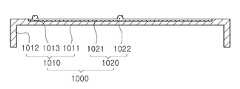
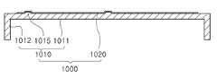
하부 수납 부재(1000)는 수납 공간을 갖는 절연성 몸체부(1010)와, 절연성 몸체부(1010)에 마련된 복수의 접지 금속부(1020)를 구비한다.The
몸체부(1010)는 상부가 개방된 박스 형태로 제작된다. 즉, 몸체부(1010)는 바닥판(1011)과, 바닥판(1011)의 내측 가장자리 영역에서 수직하게 절곡 연장된 복 수의 측벽면(1012)을 구비한다. 상기 몸체부(1010)의 수납 공간 내측으로 열 확산판(900), 반사 시트(800), 램프 유닛(500), 램프 고정 프레임(550), 열 차단판(600) 및 광학 필름부(700)가 수납된다. 이를 통해 상기 요소들의 이탈을 방지하고, 상기 요소들이 외부 충격으로 인한 손상을 방지한다.The
몸체부(1010)는 절연성 합성 수지로 제작되는 것이 효과적이다. 본 실시예에서는 폴리카보네이트(Polycarbonate; PC)를 이용하여 몸체부(1010)를 제작한다. 물론 이에 한정되지 않고, 몸체부(1010)는 폴리에틸렌테레프탈레이트(polyethyleneterephthalate; PET), 폴리에틸렌(polyethylene; PE), 폴리프로필렌(polypropylene; PP), 폴리스틸렌(polystyrene; PS), ABS(Acrylonitrile-Butadiene-Styrene) 및 스티렌 아크릴로니트릴 코폴리머(Styrene Acrylonitrile Copolymers; SAN) 중 어느 하나를 사용하여 제작할 수 있다. 이와 같이 본 실시예에서는 무거운 금속 재질이 아닌 가벼운 합성 수지를 이용하여 하부 수납 부재(1000)의 몸체부(1010)를 제작함으로 인해 하부 수납 부재(1000) 전체의 무게를 줄일 수 있다. 또한, 하부 수납 부재(1000)를 절연성 합성 수지로 제작하여 하부 수납 부재(1000) 내측의 램프(510)와 하부 수납 부재(1000) 간의 기생 커패시터를 줄여 램프(510)의 발광 균일도를 향상시킬 수 있다. 또한, 절연성 몸체부(1010)는 몸체부(1010)의 바닥판(1011) 내측표면 영역에 위치한 램프(510)의 열을 차단하는 역할을 수행할 수 있다. 이를 통해 램프(510)의 열이 몸체부(1010)의 바닥판(1011)의 외측표면에 배치된 컨트롤 보드(200), 램프 전원 공급부(1100) 및 세트 박스(1200)에 제공되는 것을 방지할 수 있다.It is effective that the
접지 금속부(1020)는 하부 수납 부재(1000)의 바닥판의 외측표면에 마련된 컨트롤 보드(200)와 램프 전원 공급부(1100)의 접지부와 접속된다. 또한, 접지 금속부(1020)는 세트 박스(1200)의 접지와 접속된다. 이와 같이 본 실시예에서는 하부 수납 부재(1000)의 몸체부(1010)에 별도로 외부 요소들(컨트롤 보드(200), 램프 전원 공급부(1100), 세트 박스(1200))의 접지를 위한 접지 금속부(1020)를 마련하여 상기 요소들의 전자파 장해(electromagnetic; EMI) 및 정전 방전(electrostatic discharge; ESD) 성능을 향상시킬 수 있다.The
상술한 바와 같이 접지 금속부(1020)에 복수의 요소들이 접속되기 때문에 접지 금속부(1020)는 복수의 영역으로 분리될 수 있다. 즉, 접지 금속부(1020)는 컨트롤 보드(200)의 접지에 전기적으로 접속된 제 1 접지 금속부(1020a)와, 램프 전원 공급부(1100)의 접지에 전기적으로 접속된 제 2 접지 금속부(1020b)와, 세트 박스(1200)의 접지에 전기적으로 접속된 제 3 접지 금속부(1020c)로 분리될 수 있다. 물론 이에 한정되지 않고, 접지 금속부(1020)에 접속되는 요소에 따라 이보다 적거나 많은 영역으로 분리될 수 있다. 즉, 접지 금속부(1020)가 복수개 마련될 수 있다.Since a plurality of elements are connected to the
상술한 제 1 내지 제 3 접지 금속부(1020a, 1020b, 1020c) 각각은 도 4에 도시된 바와 같이 절연성 몸체부(1010) 내부에 매설된 접지 금속 판(1021)과, 몸체부(1010) 외부로 돌출된 접지 돌기(1022)를 구비한다. 접지 금속 판(1021)은 도 3에 도시된 바와 같이 대략 사각 판 형상으로 제작된다. 물론 이에 한정되지 않고, 상기 접지 금속 판(1021)의 형상은 다각형 형상, 원 형상 또는 타원 형상이 가능하 다. 이때, 접지 금속 판(1021)은 전기 전도성이 우수하여 접지(즉, 그라운드)로서 역할을 할 수 있는 다양한 금속이 사용될 수 있다. 즉, 상기 금속으로 Li, Fe, Na, Mg, Al, Ca, Ti, Cr, Mn, Co, Ni, Cu, Zn, As, Sr, Mo, Pt, Ag, 및 이들의 합금으로 구성된 그룹 중 어느 하나를 사용할 수 있다. 그리고, 제 1 내지 제 3 접지 금속부(1020a, 1020b, 1020c) 각각의 접지 금속 판(1021)의 사이즈는 그 상측에 위치하는 요소들(컨트롤 보드(200), 램프 전원 공급부(1100), 세트 박스(1200))의 사이즈와 유사한 것이 효과적이다. 물론 이에 한정되지 않고, 상기 접지 금속 판(1021)의 사이즈는 상기 요소들 보다 작거나 클 수 있다.Each of the first to third
접지 금속 판(1021)에서 돌출된 접지 돌기(1022)는 앞서 설명한 바와 같이 컨트롤 보드(200), 램프 전원 공급부(1100) 또는 세트 박스(1200)의 접지부에 접속되는 접촉 패드 역할을 수행한다. 그 일 예로 도 5에 도시된 바와 같이 제 1 접지 금속부(1020a)의 접지 돌기(1022)와 컨트롤 보드(200)의 접지부(210)간의 접속을 설명한다.The
본 실시예에서는 제 1 접지 금속부(1020a)의 접지 금속 판(1021)은 몸체부(1010) 내부에 매설되고 즉, 몸체부(1010) 바닥판 내에 매립되고, 접지 돌기(1022) 만이 몸체부(1010) 외부로 돌출되어 있다. 그리고, 몸체부(1010)의 바닥판 외측표면에 컨트롤 보드(200)를 고정시킨다. 이때, 볼트, 나사 또는 후크와 같은 고정 부재를 통해 컨트롤 보드(200)를 고정시킨다. 여기서, 컨트롤 보드(200)는 몸체부(1010)에 직접 고정될 수 있다. 본 실시예의 몸체부(1010)는 가공이 용이한 합성 수지로 제작된다. 따라서, 컨트롤 보드(200) 고정을 위한 고정 부재를 몸체 부(1010)에 일체로 제작할 수도 있다. 예를 들어 몸체부(1010)의 제작시 컨트롤 보드(200) 고정을 위한 후크를 동시에 제작할 수 있다. 물론 이에 한정되지 않고, 컨트롤 보드(200)는 제 1 접지 금속부(1020a)에 고정될 수도 있다.The grounding
본 실시예에서는 컨트롤 보드(200)를 몸체부(1010)의 바닥판의 외측표면에 고정시킬 때, 컨트롤 보드(200)의 접지부(210)와 접지 돌기(1022)를 밀착시킨다. 또한, 상기 접지부(210)와 접지 돌기(1022) 간의 접속을 강화시키기 위해 별도의 결합부재(220)를 이용하여 접지부(210)와 접지 돌기(1022)를 결합시키는 것이 효과적이다. 결합부재(220)로 도 5에 도시된 바와 같이 나사를 사용할 수 있다. 즉, 이를 위해 상기 컨트롤 보드(200)의 접지부(210)에 소정의 관통홀이 마련되고, 관통홀의 상측 및 하측 주변 영역과 관통홀의 내측벽면에 접지 전극이 형성될 수 있다. 또한, 접지 돌기(1022)에도 상기 관통홀에 대응하는 홈이 형성될 수 있다. 따라서, 접지부(210)의 관통홀과 접지 돌기(1022)의 홈을 정렬 시킨 다음 관통홀과 홈 내측으로 나사를 인입시켜 관통홀 하측 주변 영역의 접지 전극과 접지 돌기(1022)의 상측면 간을 밀착 고정시킬 수 있다. 이때, 접지 돌기(1022)의 상측 영역과 관통홀 하측 주변 영역의 접지 전극이 전기적으로 접속될 뿐만 아니라 나사에 의해 컨트롤 보드(200)의 접지부(210)와 제 1 접지 금속부(1020a)의 접지 돌기(1022)가 전기적 및 기계적으로 접속될 수 있다. 본 실시예에서는 제 1 접지 금속부(1020a) 내에 복수개의 접지 돌기(1022)가 마련된다. 따라서, 이에 대응하는 컨트롤 보드(200)의 접지부(210)도 복수개 일 수 있다. 이때, 상술한 결합 부재(220)는 나사에 한정되지 않고, 볼트, 후크 및 도전성 접착제등이 사용될 수 있 다.The
이와 같이 본 실시예에서는 접지 금속부(1020)의 접지 돌기(1022) 만이 몸체부(1010) 외부로 돌출되어 컨트롤 보드(200)의 접지부(210)에 접속되고, 나머지 접지 금속 판(1021)은 몸체부(1010)내에 매립되어 있기 때문에 절연된다. 이와 같이 접지 금속 판(1021)을 노출시키지 않음으로써, 컨트롤 보드(200)의 회로 소자 및 금속 배선들과 접지 금속 판(1021) 간의 간섭 및 단락 현상을 방지할 수 있다.The
이와 같이 몸체부(1010) 내측에 접지 금속 판(1021)을 위치시키기 위해, 본 실시예에서는 몸체부(1010) 제작을 위한 사출 공정시 접지 돌기(1022)가 마련된 접지 금속 판(1021)을 삽입한다. 이를 통해 상기 몸체부(1010)와 접지 금속판(1021)이 일체로 제작될 수 있다. 즉, 합성 수지인 몸체부(1010) 사출 시 금형 내에 접지 돌기(1022)가 형성된 접지 금속 판(1021)을 배치시킨 다음 사출을 통해, 몸체부(1010) 내측에 접지 전극판(1021)을 매립시켜 하부 수납 부재(1000)를 제작한다.In this embodiment, in order to locate the grounding
본 실시예에 따른 하부 수납 부재(1000)의 구조는 상술한 실시예에 한정되지 않고, 다양한 변형예가 가능하다.The structure of the
제 1 내지 제 3 접지 금속부(1020a, 1020b, 1020c)의 일부가 분할 될 수도 있다. 도 6의 변형예에서와 같이 제 1 접지 금속부(1020a)가 제 1 접지 금속 영역(1020a-1)과 제 2 접지 금속 영역(1020a-2)으로 분할될 수 있다. 여기서, 제 1 접지 금속 영역(1020a-1)과 제 2 접지 금속 영역(1020a-2) 각각은 각기 컨트롤 보드(200)의 접지부(210)에 접속된다. 이로인해 제 1 접지 금속 영역(1020a-1)과 제 2 접지 금속 영역(1020a-2)은 동일 전위를 유지할 수 있다. 또한, 도 6에 도시된 바와 같이 제 1 접지 금속부(1020a)의 제 1 접지 금속 영역(1020a-1)과 제 3 접지 금속부(1020-c)가 연결될 수도 있다. 이를 통해 제 3 접지 금속부(1020-c)에 접속되는 세트 박스(1200)의 접지부의 접지 레벨과 제 1 접지 금속부(1020a)에 접속되는 컨트롤 보드(200)의 접지부의 접지 레벨을 동일하게 할 수 있다.A part of the first to third
도 7의 변형예에서와 같이 상기 제 1 내지 제 3 접지 금속부(1020a, 1020b, 1020c)를 단일의 접지 전극판(1021)으로 제작할 수 있다. 이를 통해 제 1 내지 제 3 접지 금속부(1020a, 1020b, 1020c)의 전위를 동일하게 유지할 수 있다.The first to third
도 8의 변형예에서와 같이 접지 금속부(1020)가 몸체부(1010) 내부에 매설되지 않고, 몸체부(1010)의 바닥판(1011)의 외측표면 상에 부착될 수도 있다. 즉, 사출 공정을 통해 몸체부(1010)를 제작한 다음, 몸체부(1010)의 바닥판(1011) 외측표면에 접지 돌기(1022)가 마련된 복수의 접지 금속 판(1021)을 고정시켜 접지 금속부(1020)를 제작한다. 이를 통해 몸체부(1010)에 접지 금속부(1020)가 고정된 하부 수납 부재(1000)를 제작할 수 있다. 이때, 접지 금속 판(1021)의 고정을 위해 나사, 볼트, 후크 및 접착제가 사용될 수 있다.The
도 9의 변형예에서와 같이 하부 수납 부재(1000)의 바닥판(1011)의 두께 증가를 방지하기 위해 몸체부(1010)의 바닥판(1011) 외측표면에 오목홈을 형성하고, 상기 오목홈 내에 접지 금속 판(1021)을 끼워 넣어 접지 금속부(1020)를 갖는 하부 수납 부재(1000)를 제작할 수도 있다. 즉, 사출 공정을 통해 바닥판(1011) 외측표면에 복수의 오목홈(1013)이 형성된 절연성 몸체부(1010)를 제작한다. 오목홈(1013) 내측으로 접지 돌기(1022)가 마련된 접지 금속 판(1021)을 삽입 고정시켜 접지 금속부(1020)를 제작한다. 이때, 접지 금속 판(1021)은 나사, 볼트, 후크 및 접착제를 포함하는 고정 부재를 통해 상기 몸체부(1010)에 고정되는 것이 효과적이다.A concave groove is formed on the outer surface of the
도 10의 변형예에서와 같이 몸체부(1010)의 바닥판(1011)에 관통홀(1014)을 형성하고, 상기 관통홀(1014)에 접지 금속 판(1021)을 삽입시켜 접지 금속부(1020)를 갖는 하부 수납 부재(1000)를 제작할 수 있다. 이때, 관통홀(1014)의 내측벽과 접지 금속 판(1021)의 외측벽(상기 관통홀(1014)의 내측벽면에 접한 벽면)에는 요철 패턴이 마련되는 것이 효과적이다. 이를 통해 접지 금속 판(1021)을 관통홀(1014) 내측에서 고정시킬 수 있다. 또한, 상술한 접착제등의 고정부재를 더 구비하여 접지 금속 판(1021)이 관통홀(1014)에서 떨어져 나가는 것을 방지할 수 있다.10, a through
도 11의 변형예에서와 같이 몸체부(1010)의 바닥판(1011) 내측표면에 접지 금속 판(1021)을 부착시킬 수도 있다. 이때, 접지 금속 판(1021)의 접지 돌기(1022)는 몸체부(1010)의 바닥판(1011)을 관통하여 몸체부(1010)의 바닥판(1011)의 외측표면으로 돌출될 수 있다.The
도 12의 변형예에서와 같이 몸체부(1010)의 바닥판(1011)의 외측표면 상에 접지 금속부(1020)를 얇은 박막 형태로 형성할 수도 있다. 이때, 몸체부(1010)의 바닥판(1011) 외측표면에 앞서 설명한 실시예의 접지 돌기(1022)에 해당하는 돌출부(1015)가 형성되는 것이 효과적이다. 이를 통해 상기 돌출부(1015) 상측에 형성된 박막 형태의 접지 금속부(1020)가 컨트롤 보드(200)의 접지부(210)에 접속될 수 있다. 상기 박막 형태의 접지 금속부(1020)는 인쇄 방법을 통해 금속 박막을 몸체부(1010)의 바닥판(1011) 외측표면에 형성하여 제작할 수 있다. 또한, 금속 박막 증착 공정을 통해 형성할 수도 있다. 또한, 얇은 금속 성의 박막을 몸체부(1010)의 바닥판(1011) 외측표면에 부착하여 제작할 수도 있다.The
도 13의 변형예에서와 같이 접지 금속부(1020)의 접지 돌기(1022)는 접지 금속 판(1021)의 일부를 돌출시켜 제작할 수도 있다. 즉, 접지 금속판의 일부를 절곡시켜 돌기를 제작할 수 있다.The
도 14의 변형예에서와 같이 접지 금속부(1020)는 몸체부(1010) 내에 판 형상으로 매립될 수 있다. 그리고, 몸체부(1010)의 바닥판(1011) 외측표면에는 접지 금속부(1020)를 노출시키는 복수의 노출홈(1015)이 마련될 수 있다. 이를 통해 접지 돌기(1022)를 제작하지 않을 수 있다. 이때, 컨트롤 보드(200)등 각종 부재의 접지부(210)는 돌출된 형상으로 제작되는 것이 효과적이다. 따라서, 돌출된 형상의 접지부(210)가 노출홈(1015) 내측으로 인입되어 노출홈(1015)에 의해 노출된 접지 금속부(1020)과 전기적으로 접속될 수 있다.14, the
또한, 도 15의 변형예에서와 같이 몸체부(1010)의 노출홈(1015) 내부를 도전성 물질로 매립하여 접지 콘택(1030)을 형성할 수도 있다. 상기 접지 콘택(1030)을 통해 컨트롤 보드(200)의 접지부와 접지 금속부(1020)간을 전기적으로 연결시킬 수 있다.15, the
또한, 도 16의 변형예에서와 같이 몸체부(1010)의 바닥판(1011) 내측표면에 램프(510)를 지지하는 램프 지지 홀더(1040)를 형성할 수도 있다. 본 실시예의 몸 체부(1010)를 가공이 용이한 합성 수지를 사용하기 때문에 몸체부(1010) 제작시 램프 지지 홀더(1040)도 함께 제작할 수 있다. 즉, 램프 지지 홀더(1040)를 몸체부(1010)와 일체로 제작할 수 있다. 물론 램프 서포트도 몸체부(1010)와 일체로 제작할 수 있다. 이를 통해 표시 장치 제작을 위한 부품수를 줄일 수 있고, 부품들의 조립을 위한 시간을 절약할 수 있어 표시 장치의 제작 시간을 줄일 수 있다.16, a
또한, 도시되지 않았지만, 상술한 접지 금속부(1020)를 다층 전극 판으로 제작할 수도 있다.Further, although not shown, the above-described
상술한 실시예의 디스플레이 어셈블리(10)는 액정 표시 패널(100)을 구비한다. 하지만, 액정 표시 패널(100) 대신 플라즈마 디스플레이 패널(Plasma Display Panel; PDP) 또는 능동형 유기 발광 다이오드(Active Matrix Organic Light Emitting Diode; AM-OLED)등이 사용될 수도 있다. 또한, 상술한 실시예에서는 복수의 램프가 액정 표시 패널(100) 하측에 균일하게 배열된 직하형의 백라이트 어셈블리(20)에 관해 설명하였지만, 이에 한정되지 않고, 도광판을 이용한 에지형의 백라이트 어셈블리에 적용될 수도 있다. 그리고, 상기 사용되는 패널에 따라 상기 하부 수납 부재를 제외한 광원부가 생략될 수도 있다.The
본 발명을 첨부 도면과 전술된 바람직한 실시예를 참조하여 설명하였으나, 본 발명은 그에 한정되지 않으며, 후술되는 특허청구범위에 의해 한정된다. 따라서, 본 기술분야의 통상의 지식을 가진 자라면 후술되는 특허청구범위의 기술적 사상에서 벗어나지 않는 범위 내에서 본 발명을 다양하게 변형 및 수정할 수 있다.Although the present invention has been described with reference to the accompanying drawings and the preferred embodiments described above, the present invention is not limited thereto but is limited by the following claims. Accordingly, those skilled in the art will appreciate that various modifications and changes may be made thereto without departing from the spirit of the following claims.
도 1은 본 발명의 일 실시예에 따른 표시 장치의 분해 사시도.1 is an exploded perspective view of a display device according to an embodiment of the present invention;
도 2는 일 실시예에 따른 표시 장치의 조립 단면도.2 is an assembled sectional view of a display device according to one embodiment.
도 3은 일 실시예에 따른 하부 수납 부재와 이에 고정되는 요소들을 설명하기 위한 분해 사시도.3 is an exploded perspective view for explaining a lower housing member and elements fixed thereto according to an embodiment;
도 4는 일 실시예에 따른 하부 수납 부재의 단면도.4 is a cross-sectional view of a lower receiving member according to one embodiment.
도 5는 일 실시예에 따른 하부 수납 부재에 일 요소가 접속된 단면도.5 is a cross-sectional view of an element connected to a lower housing member according to an embodiment;
도 6 및 도 7은 일 실시예의 변형예에 따른 하부 수납 부재의 평면도.Figs. 6 and 7 are plan views of a lower housing member according to a modification of the embodiment; Fig.
도 8 내지 16은 일 실시예의 변형예에 따른 하부 수납 부재의 단면도.8 to 16 are sectional views of a lower housing member according to a modification of the embodiment.
<도면의 주요 부분에 대한 부호의 설명>Description of the Related Art
10 : 디스플레이 어셈블리20 : 백라이트 어셈블리10: display assembly 20: backlight assembly
100 : 액정 표시 패널200 : 컨트롤 보드100: liquid crystal display panel 200: control board
400 : 상부 수납 부재1000 : 하부 수납 부재400: upper housing member 1000: lower housing member
1010 : 몸체부1020 : 접지 금속부1010: Body part 1020: Ground metal part
1021 : 접지 금속 판1022 : 접지 돌기1021: grounding metal plate 1022: grounding projection
1100 : 램프 전원 공급부1200 : 세트 박스1100: lamp power supply unit 1200: set box
Claims (20)
Translated fromKoreanPriority Applications (2)
| Application Number | Priority Date | Filing Date | Title |
|---|---|---|---|
| KR1020080004406AKR101438647B1 (en) | 2008-01-15 | 2008-01-15 | Container member and flat display apparatus having the same |
| US12/185,883US20090180048A1 (en) | 2008-01-15 | 2008-08-05 | Receiving member, display having the same, and method thereof |
Applications Claiming Priority (1)
| Application Number | Priority Date | Filing Date | Title |
|---|---|---|---|
| KR1020080004406AKR101438647B1 (en) | 2008-01-15 | 2008-01-15 | Container member and flat display apparatus having the same |
Publications (2)
| Publication Number | Publication Date |
|---|---|
| KR20090078530A KR20090078530A (en) | 2009-07-20 |
| KR101438647B1true KR101438647B1 (en) | 2014-09-17 |
Family
ID=40850329
Family Applications (1)
| Application Number | Title | Priority Date | Filing Date |
|---|---|---|---|
| KR1020080004406AExpired - Fee RelatedKR101438647B1 (en) | 2008-01-15 | 2008-01-15 | Container member and flat display apparatus having the same |
Country Status (2)
| Country | Link |
|---|---|
| US (1) | US20090180048A1 (en) |
| KR (1) | KR101438647B1 (en) |
Families Citing this family (13)
| Publication number | Priority date | Publication date | Assignee | Title |
|---|---|---|---|---|
| EP2367411A3 (en)* | 2010-03-17 | 2015-03-18 | Kabushiki Kaisha Toshiba | Display apparatus and electronic apparatus |
| US8724044B2 (en)* | 2011-11-01 | 2014-05-13 | Shenzhen China Star Optoelectronics Technology Co., Ltd. | Liquid crystal display based on insulation backplane |
| CN102385180A (en)* | 2011-11-01 | 2012-03-21 | 深圳市华星光电技术有限公司 | Liquid crystal display device based on insulated back plate |
| JP6025324B2 (en)* | 2011-12-15 | 2016-11-16 | 三菱電機株式会社 | Liquid crystal display |
| DE102012203955A1 (en)* | 2012-03-14 | 2013-09-19 | Zf Friedrichshafen Ag | Mounting frame for electronic device e.g. data encryption apparatus, has support portion that is provided for supporting heat guide plate for heat dissipation of electric circuit of circuit board |
| WO2013184150A1 (en)* | 2012-06-08 | 2013-12-12 | Apple Inc. | Internal components of a portable computing device |
| CN103676274B (en)* | 2013-11-21 | 2016-03-09 | 苏州佳世达电通有限公司 | Display |
| KR102209743B1 (en) | 2014-06-11 | 2021-02-01 | 삼성디스플레이 주식회사 | Display apparatus and method of driving thereof |
| JP6437338B2 (en) | 2015-02-17 | 2018-12-12 | 富士通クライアントコンピューティング株式会社 | Housing and electronic equipment |
| KR102345612B1 (en)* | 2015-07-08 | 2022-01-03 | 삼성디스플레이 주식회사 | Display device |
| WO2020226369A1 (en)* | 2019-05-03 | 2020-11-12 | Samsung Electronics Co., Ltd. | Light emitting diode module |
| CN112449515A (en)* | 2019-08-27 | 2021-03-05 | Oppo广东移动通信有限公司 | Shell and manufacturing method thereof |
| EP3944010B1 (en)* | 2020-07-23 | 2023-02-15 | Ficosa Adas, S.L.U. | Display assembly for an imaging device |
Citations (4)
| Publication number | Priority date | Publication date | Assignee | Title |
|---|---|---|---|---|
| JPS60144997A (en)* | 1983-12-14 | 1985-07-31 | テクトロニツクス・インコーポレイテツド | Chassis for electronic device |
| KR19990045438A (en)* | 1997-11-17 | 1999-06-25 | 오카모토 세이시 | Flat Panel Display |
| KR20060057187A (en)* | 2004-11-23 | 2006-05-26 | 삼성전자주식회사 | Storage container for display device and liquid crystal display device having same |
| US7503685B2 (en)* | 2005-09-20 | 2009-03-17 | Toshiba Matsushita Display Technology Co., Ltd. | Illumination unit and liquid crystal display device using the same |
Family Cites Families (16)
| Publication number | Priority date | Publication date | Assignee | Title |
|---|---|---|---|---|
| US5285350A (en)* | 1992-08-28 | 1994-02-08 | Aavid Engineering, Inc. | Heat sink plate for multiple semi-conductors |
| US5519168A (en)* | 1993-10-12 | 1996-05-21 | Owens; William M. | Electromagnetic interference shielding |
| JP3442877B2 (en)* | 1994-02-21 | 2003-09-02 | 富士通株式会社 | Resin molded product and manufacturing method thereof |
| US6738265B1 (en)* | 2000-04-19 | 2004-05-18 | Nokia Mobile Phones Ltd. | EMI shielding for portable electronic devices |
| US6734463B2 (en)* | 2001-05-23 | 2004-05-11 | Semiconductor Energy Laboratory Co., Ltd. | Semiconductor device comprising a window |
| KR100783609B1 (en)* | 2001-07-10 | 2007-12-07 | 삼성전자주식회사 | Liquid crystal display |
| JP2003195263A (en)* | 2001-12-27 | 2003-07-09 | Fujitsu Display Technologies Corp | Liquid crystal display |
| US7298624B2 (en)* | 2002-05-28 | 2007-11-20 | Xyratex Technology Limited | Data storage device chassis, case and clamp mechanism |
| US7209368B2 (en)* | 2003-01-30 | 2007-04-24 | Endicott Interconnect Technologies, Inc. | Circuitized substrate with signal wire shielding, electrical assembly utilizing same and method of making |
| US20050073822A1 (en)* | 2003-10-07 | 2005-04-07 | Ya-Wen Hsu | Electromagnetic interference shielding assembly |
| TW200515036A (en)* | 2003-10-17 | 2005-05-01 | Au Optronics Corp | Grounding device of liquid crystal display circuit board |
| US7342184B2 (en)* | 2005-03-15 | 2008-03-11 | Stealthdrive, Inc. | Three-dimensional configurations providing electromagnetic interference shielding for electronics enclosures |
| JP4786366B2 (en)* | 2006-02-20 | 2011-10-05 | 日立プラズマディスプレイ株式会社 | Plasma display device |
| KR101283973B1 (en)* | 2006-06-16 | 2013-07-09 | 엘지디스플레이 주식회사 | Backlight unit and LC display device |
| KR100879300B1 (en)* | 2007-04-24 | 2009-01-19 | 삼성에스디아이 주식회사 | Plasma display device |
| JP2009210883A (en)* | 2008-03-05 | 2009-09-17 | Canon Inc | Image display device |
- 2008
- 2008-01-15KRKR1020080004406Apatent/KR101438647B1/ennot_activeExpired - Fee Related
- 2008-08-05USUS12/185,883patent/US20090180048A1/ennot_activeAbandoned
Patent Citations (4)
| Publication number | Priority date | Publication date | Assignee | Title |
|---|---|---|---|---|
| JPS60144997A (en)* | 1983-12-14 | 1985-07-31 | テクトロニツクス・インコーポレイテツド | Chassis for electronic device |
| KR19990045438A (en)* | 1997-11-17 | 1999-06-25 | 오카모토 세이시 | Flat Panel Display |
| KR20060057187A (en)* | 2004-11-23 | 2006-05-26 | 삼성전자주식회사 | Storage container for display device and liquid crystal display device having same |
| US7503685B2 (en)* | 2005-09-20 | 2009-03-17 | Toshiba Matsushita Display Technology Co., Ltd. | Illumination unit and liquid crystal display device using the same |
Also Published As
| Publication number | Publication date |
|---|---|
| KR20090078530A (en) | 2009-07-20 |
| US20090180048A1 (en) | 2009-07-16 |
Similar Documents
| Publication | Publication Date | Title |
|---|---|---|
| KR101438647B1 (en) | Container member and flat display apparatus having the same | |
| US7909480B2 (en) | Light source module, method of fabricating the same, and display device having the light source module | |
| US7819574B2 (en) | Backlight assembly and display device having the same | |
| JP6126254B2 (en) | Backlight assembly | |
| US6667780B2 (en) | Liquid crystal display module and liquid crystal display apparatus having the same | |
| KR101406978B1 (en) | Liquid crystal display device and method of combining the same | |
| KR101930521B1 (en) | Display module of display device | |
| US20070236910A1 (en) | Covering member for display device, display device having the same, and method thereof | |
| KR20090048075A (en) | Display device | |
| KR101318757B1 (en) | Liquid crystal display | |
| CN103140795A (en) | Liquid crystal display device | |
| KR20070113838A (en) | Printed circuit board for flat panel display device and flat panel display device having same | |
| KR20070119872A (en) | Backlight Assembly and Liquid Crystal Display | |
| KR20080077827A (en) | Light emitting diode block, backlight unit and liquid crystal display using the same | |
| KR101255279B1 (en) | Backlight Unit | |
| KR20090121101A (en) | Backlight assembly and display device including same | |
| JP2010271629A (en) | Display device | |
| KR100962644B1 (en) | LCD Display | |
| KR20070088117A (en) | Backlight unit and liquid crystal display device using same | |
| KR101623587B1 (en) | Liquid Crystal Display | |
| KR20110045370A (en) | LCD Display | |
| KR20050005167A (en) | Liquid crystal display device | |
| KR20090008581A (en) | Liquid crystal display | |
| KR20050087232A (en) | Liquid crystal display provided with a shield case for discharging heat | |
| KR20060104755A (en) | Display device |
Legal Events
| Date | Code | Title | Description |
|---|---|---|---|
| PA0109 | Patent application | St.27 status event code:A-0-1-A10-A12-nap-PA0109 | |
| R17-X000 | Change to representative recorded | St.27 status event code:A-3-3-R10-R17-oth-X000 | |
| PG1501 | Laying open of application | St.27 status event code:A-1-1-Q10-Q12-nap-PG1501 | |
| R18-X000 | Changes to party contact information recorded | St.27 status event code:A-3-3-R10-R18-oth-X000 | |
| N231 | Notification of change of applicant | ||
| PN2301 | Change of applicant | St.27 status event code:A-3-3-R10-R13-asn-PN2301 St.27 status event code:A-3-3-R10-R11-asn-PN2301 | |
| A201 | Request for examination | ||
| PA0201 | Request for examination | St.27 status event code:A-1-2-D10-D11-exm-PA0201 | |
| E902 | Notification of reason for refusal | ||
| PE0902 | Notice of grounds for rejection | St.27 status event code:A-1-2-D10-D21-exm-PE0902 | |
| E13-X000 | Pre-grant limitation requested | St.27 status event code:A-2-3-E10-E13-lim-X000 | |
| P11-X000 | Amendment of application requested | St.27 status event code:A-2-2-P10-P11-nap-X000 | |
| P13-X000 | Application amended | St.27 status event code:A-2-2-P10-P13-nap-X000 | |
| E701 | Decision to grant or registration of patent right | ||
| PE0701 | Decision of registration | St.27 status event code:A-1-2-D10-D22-exm-PE0701 | |
| GRNT | Written decision to grant | ||
| PR0701 | Registration of establishment | St.27 status event code:A-2-4-F10-F11-exm-PR0701 | |
| PR1002 | Payment of registration fee | St.27 status event code:A-2-2-U10-U11-oth-PR1002 Fee payment year number:1 | |
| PG1601 | Publication of registration | St.27 status event code:A-4-4-Q10-Q13-nap-PG1601 | |
| R18-X000 | Changes to party contact information recorded | St.27 status event code:A-5-5-R10-R18-oth-X000 | |
| LAPS | Lapse due to unpaid annual fee | ||
| PC1903 | Unpaid annual fee | St.27 status event code:A-4-4-U10-U13-oth-PC1903 Not in force date:20170902 Payment event data comment text:Termination Category : DEFAULT_OF_REGISTRATION_FEE | |
| PC1903 | Unpaid annual fee | St.27 status event code:N-4-6-H10-H13-oth-PC1903 Ip right cessation event data comment text:Termination Category : DEFAULT_OF_REGISTRATION_FEE Not in force date:20170902 | |
| R18-X000 | Changes to party contact information recorded | St.27 status event code:A-5-5-R10-R18-oth-X000 |