KR101438355B1 - Linear analog optical transmitter with IM3 cancellation function - Google Patents
Linear analog optical transmitter with IM3 cancellation functionDownload PDFInfo
- Publication number
- KR101438355B1 KR101438355B1KR1020130062815AKR20130062815AKR101438355B1KR 101438355 B1KR101438355 B1KR 101438355B1KR 1020130062815 AKR1020130062815 AKR 1020130062815AKR 20130062815 AKR20130062815 AKR 20130062815AKR 101438355 B1KR101438355 B1KR 101438355B1
- Authority
- KR
- South Korea
- Prior art keywords
- signal
- diode
- path
- phase
- schottky diode
- Prior art date
- Legal status (The legal status is an assumption and is not a legal conclusion. Google has not performed a legal analysis and makes no representation as to the accuracy of the status listed.)
- Expired - Fee Related
Links
Images


Classifications
- H—ELECTRICITY
- H04—ELECTRIC COMMUNICATION TECHNIQUE
- H04B—TRANSMISSION
- H04B10/00—Transmission systems employing electromagnetic waves other than radio-waves, e.g. infrared, visible or ultraviolet light, or employing corpuscular radiation, e.g. quantum communication
- H04B10/50—Transmitters
- H04B10/58—Compensation for non-linear transmitter output
- H—ELECTRICITY
- H04—ELECTRIC COMMUNICATION TECHNIQUE
- H04B—TRANSMISSION
- H04B10/00—Transmission systems employing electromagnetic waves other than radio-waves, e.g. infrared, visible or ultraviolet light, or employing corpuscular radiation, e.g. quantum communication
- H04B10/50—Transmitters
- H04B10/501—Structural aspects
- H04B10/503—Laser transmitters
- H—ELECTRICITY
- H10—SEMICONDUCTOR DEVICES; ELECTRIC SOLID-STATE DEVICES NOT OTHERWISE PROVIDED FOR
- H10D—INORGANIC ELECTRIC SEMICONDUCTOR DEVICES
- H10D8/00—Diodes
- H10D8/01—Manufacture or treatment
- H10D8/051—Manufacture or treatment of Schottky diodes
Landscapes
- Physics & Mathematics (AREA)
- Electromagnetism (AREA)
- Engineering & Computer Science (AREA)
- Computer Networks & Wireless Communication (AREA)
- Signal Processing (AREA)
- Nonlinear Science (AREA)
- Optics & Photonics (AREA)
- Optical Communication System (AREA)
Abstract
Translated fromKoreanDescription
Translated fromKorean본 발명은 광송신기에 관한 것으로, 보다 상세하게 쇼트키 다이오드를 이용한 IM3 소거 기능을 갖는 선형 아날로그 광송신기에 관한 것이다.The present invention relates to an optical transmitter, and more particularly to a linear analog optical transmitter having an IM3 cancellation function using a Schottky diode.
모바일 트래픽 급증으로 인해, 최근 스몰셀에 대한 중요성이 증가하고 있다. 이에, 국내 ISP(internet service provider)는 Wi-Fi 망을 구축하고 있으며, 통신사에서도 펨토셀(femto cell) 개발을 추진하고 있는 실정이다.Due to the surge in mobile traffic, the importance of the recent small cell is increasing. Accordingly, a domestic ISP (Internet service provider) is establishing a Wi-Fi network, and a femto cell is being developed in a telecommunication company.
이러한 스몰셀의 주요 역할로 데이터 트래픽이 밀집된 지역에서 네트워크 부하 분산과, 매크로셀 (macro cell)의 커버리지가 미치지 못하는 통신 음역지역을 보완하는 역할을 동시에 수행할 수 있어야 한다.The main role of such a small cell should be to simultaneously perform network load balancing in a region where data traffic is dense, and complementary to a communication range in which macro cell coverage is insufficient.
Fi-Wi (fiber wireless) 시스템은 저손실, 광대역, 초고속 전송 등의 광통신 기술의 장점을 가지고 있고, 원격지 노드의 RF 신호를 기지국에서 그대로 받아 원격지의 채널 상태 및 트래픽을 제어할 수 있어 네트워크의 트래픽 분산을 유도할 수 있으며 중ㆍ장거리 네트워크 구성이 용이한 장점을 가지고 있다.Wi-Fi (fiber wireless) system has advantages of optical communication technology such as low loss, broadband and high speed transmission, and it can control remote channel condition and traffic by receiving RF signal of remote node directly from base station, And it is easy to construct a medium and long distance network.
Fi-Wi 시스템을 구축하기 위한 광통신 시스템은 LD (laser diode)에 마이크로파 대역의 RF 신호를 직접 변조하는 아날로그 SCM (sub-carrier multiplexing) 광 전송방식이다.An optical communication system for building a Fi-Wi system is an analog sub-carrier multiplexing (SCM) optical transmission system that directly modulates an RF signal in a microwave band to a laser diode (LD).
이러한 비선형으로 인한 주파수 성분들은 아날로그 신호를 왜곡하고, 전송 대역폭 안에 놓여 시스템의 성능을 열화시키는 단점이 있다.These nonlinear frequency components have the disadvantage of distorting the analog signal and degrading the performance of the system in the transmission bandwidth.
도 1은 종래의 프리디스토션 기반의 광송신기의 구성을 도시한 블록도이다.1 is a block diagram showing a configuration of a conventional predistortion-based optical transmitter.
도 1을 참조하면, 메이저 루프(major loop)에서는 RF 신호에 대해 딜레이만 시키고, 딜레이 시킨 RF 신호의 위상을 180도 변환한 후 합쳐 LD(laser diode)로 입력하는 구조이다.Referring to FIG. 1, in a major loop, only a delay is applied to an RF signal, a phase of a delayed RF signal is converted to 180 degrees, and the resultant signal is input to a laser diode (LD).
이러한 종래의 프리디스토션 기반의 광송신기의 단점은 LD의 비선형성을 동일한 광소자인 LD를 이용하여 제거하는 구조로 가격적인 측면에서도 비용이 높을 뿐만 아니라, 마이너 루프(minor loop)에서 LD와 PD(photo diode)를 사용하여 PD 자체가 효율이 좋지 않아 시스템적인 측면에서 insertion loss가 커지게 되어 능동소자인 증폭기를 반드시 사용해야만 LD의 비선형성을 제거할 수 있는 단점이 있으며 더불어 전력 소모도 커지는 단점이 있다.A disadvantage of such a conventional predistortion-based optical transmitter is that the nonlinearity of the LD is eliminated by using an LD that is the same optical device, which not only is costly in terms of cost, but also the LD and PD (photo diode is used, the efficiency of the PD itself is poor, so that the insertion loss is increased in terms of the system, so that the nonlinearity of the LD can be removed only by using the active device amplifier, and the power consumption is also increased .
본 발명은 쇼트키 다이오드를 이용한 IM3 소거 기능을 갖는 선형 아날로그 광송신기를 제공하기 위한 것이다.The present invention is to provide a linear analog optical transmitter having an IM3 cancellation function using a Schottky diode.
이를 통해, 본 발명은 종래의 기존 LD(laser) 및 PD(photodiode)를 이용하여 비선형 성분을 생성할 때에 비해 전체 구조를 간소화하고, 적은 수의 전자소자를 이용하여 광송신기를 구성할 수 있어 가격이 저렴해지고 소비 전력을 줄일 수 있는 IM3 소거 기능을 갖는 선형 아날로그 광송신기를 제공하기 위한 것이다.Accordingly, the present invention can simplify the entire structure and constitute an optical transmitter by using a small number of electronic elements, compared with a conventional non-linear component using LD (laser) and PD (photodiode) And to provide a linear analog optical transmitter having an IM3 cancellation function that can be made inexpensive and reduce power consumption.
발명의 일 측면에 따르면, 쇼트키 다이오드를 이용하여 비선형 성분을 생성할 수 있는 프리디스토터 및 그 프리티스토터에 기반한 IM3 소거 기능을 갖는 선형 아날로그 광송신기가 제공된다.According to an aspect of the invention, there is provided a predistorter capable of generating a non-linear component using a Schottky diode and a linear analog optical transmitter having an IM3 cancellation function based on the pristestor.
본 발명의 일 실시예에 따르면, 투톤(two-tone) RF 신호를 제1 경로 및 제2 경로로 분배하는 분배부; 상기 제1 경로의 RF 신호를 지연하는 지연부; 상기 제2 경로의 RF 신호를 입력받아 비선형 신호를 생성하는 다이오드 블록; 상기 다이오드 블록으로부터 상기 비선형 신호를 입력받아 위상을 조절하는 위상 조절부; 및 상기 위상 조절부를 통해 위상 조절된 상기 비선형 신호와 상기 지연부를 통해 지연된 RF 신호를 결합하는 결합부를 포함하는 프리디스토터가 제공될 수 있다.According to an embodiment of the present invention, there is provided an RF receiver including: a distributor for distributing a two-tone RF signal to a first path and a second path; A delay unit for delaying the RF signal of the first path; A diode block receiving the RF signal of the second path and generating a nonlinear signal; A phase adjuster for receiving the nonlinear signal from the diode block and adjusting the phase; And a coupling unit coupling the non-linear signal phase-adjusted through the phase adjusting unit and the RF signal delayed through the delay unit.
상기 위상 조절부는 상기 비선형 신호를 상기 제1 경로의 RF 신호와의 위상차가 180도 차이 나도록 위상을 조절할 수 있다.The phase adjusting unit may adjust the phase of the nonlinear signal so that the phase difference between the nonlinear signal and the RF signal of the first path is 180 degrees.
상기 다이오드 블록은 쇼트키 다이오드, 복수의 매칭부를 더 포함하되,The diode block may further include a Schottky diode and a plurality of matching units,
상기 매칭부는 상기 쇼트키 다이오드 전단 및 후단에 각각 연결된다.The matching unit is connected to the front end and the rear end of the Schottky diode, respectively.
상기 매칭부는 병렬로 유입되는 직류(DC) 바이어스의 유출을 방지하기 위한 DC 블록 기능을 수행하는 캐패시터; 및 교류(AC) 성분이 상기 DC 블록으로 유입되는 것을 방지하는 인덕터를 포함한다.Wherein the matching unit includes: a capacitor that performs a DC blocking function to prevent leakage of DC bias introduced in parallel; And an inductor that prevents an AC component from entering the DC block.
상기 쇼트키 다이오드 전단에 배치되는 제1 매칭부의 인덕터는 접지와 연결되며,The inductor of the first matching unit disposed at the front end of the Schottky diode is connected to the ground,
상기 쇼트키 다이오드 후단에 배치되는 제2 매칭부의 인덕터는 저항과 연결된다.
The inductor of the second matching part disposed at the rear end of the Schottky diode is connected to a resistor.
본 발명의 다른 실시예에 따르면, 쇼트키 다이오드를 이용하여 비선형 신호를 생성한 후 지연된 RF 신호와 결합하여 출력하는 프리디스토터; 및 상기 프리디스토터를 통해 출력된 RF 신호를 전송하는 전송부를 포함하는 프리디스토션 기반의 광송신기가 제공될 수 있다.According to another embodiment of the present invention, there is provided a predistorter comprising: a predistorter for generating a non-linear signal using a Schottky diode and combining the signal with a delayed RF signal; And a transmitter for transmitting the RF signal output through the predistorter.
투톤(two-tone) RF 신호를 제1 경로 및 제2 경로로 분배하는 분배부; 상기 제1 경로의 RF 신호를 지연하는 지연부; 쇼트키 다이오드를 포함하며, 상기 쇼트키 다이오드를 이용하여 상기 제2 경로의 RF 신호를 입력받아 비선형 신호를 생성하는 다이오드 블록; 상기 다이오드 블록으로부터 상기 비선형 신호를 입력받아 위상을 조절하는 위상 조절부; 및 상기 위상 조절부를 통해 위상 조절된 상기 비선형 신호와 상기 지연부를 통해 지연된 RF 신호를 결합하는 결합부를 포함할 수 있다.A distribution unit for distributing the two-tone RF signal to the first path and the second path; A delay unit for delaying the RF signal of the first path; A diode block including a Schottky diode and receiving the RF signal of the second path using the Schottky diode to generate a nonlinear signal; A phase adjuster for receiving the nonlinear signal from the diode block and adjusting the phase; And a combining unit for combining the nonlinear signal phase-adjusted through the phase adjusting unit and the RF signal delayed through the delay unit.
상기 전송부는 LD(laser diode)를 포함한다.The transmitter includes a laser diode (LD).
본 발명의 일 실시예에 따른 IM3 소거 기능을 갖는 선형 아날로그 광송신기를 제공함으로써, 종래의 기존 LD(laser) 및 PD(photodiode)를 이용하여 비선형 성분을 생성할 때에 비해 전체 구조를 간소화하고, 적은 수의 전자소자를 이용하여 광송신기를 구성할 수 있어 가격이 저렴해지고 소비 전력을 줄일 수 있는 이점이 있다.
The present invention provides a linear analog optical transmitter having an IM3 cancellation function according to an exemplary embodiment of the present invention to simplify the entire structure and reduce the number of components, It is possible to construct an optical transmitter by using a number of electronic devices, which makes it possible to reduce the cost and reduce power consumption.
도 1은 종래의 방법에 따른 프리디스토션 기반의 광송신기를 나타낸 블록도.
도 2는 본 발명의 일 실시예에 따른 IM3 소거 기능을 갖는 선형 아날로그 광송신기의 구성을 나타낸 블록도.
도 3은 본 발명의 일 실시예에 다른 다이오드 블록의 상세 구조를 나타낸 회로도.
도 4는 본 발명의 일 실시예에 따른 쇼트키 다이오드를 순방향 및 역방향으로 직렬 연결한 다이오드 블록의 구조를 도시한 도면.
도 5는 도 4의 다이오드 블록의 구조에 따른 바이어스 전압에 따른 비선형 신호를 나타낸 도면.
도 6은 본 발명의 일 실시예에 따른 쇼트키 다이오드를 순방향과 역방향으로 병렬 연결한 다이오드 블록의 구조를 도시한 도면.
도 7은 도 6의 다이오드 블록 구조에 따른 바이어스 전압에 따른 비선형 신호를 나타낸 도면.
도 8은 본 발명의 일 실시예에 따른 쇼트키 다이오드를 이용하여 비선형 신호를 생성한 후 이를 제거한 결과에 따른 실험 결과를 나타낸 그래프.1 is a block diagram showing a predistortion-based optical transmitter according to a conventional method;
2 is a block diagram illustrating a configuration of a linear analog optical transmitter having an IM3 erase function according to an exemplary embodiment of the present invention;
3 is a circuit diagram showing a detailed structure of a diode block according to an embodiment of the present invention.
4 is a diagram illustrating a structure of a diode block in which Schottky diodes are connected in series in a forward direction and a reverse direction according to an embodiment of the present invention.
FIG. 5 is a diagram illustrating a non-linear signal according to a bias voltage according to the structure of the diode block of FIG. 4;
6 is a diagram illustrating a structure of a diode block in which a Schottky diode is connected in parallel in forward and reverse directions according to an embodiment of the present invention.
FIG. 7 is a diagram illustrating a non-linear signal according to a bias voltage according to the diode block structure of FIG. 6;
FIG. 8 is a graph illustrating experimental results of generating and outputting a nonlinear signal using a Schottky diode according to an embodiment of the present invention. Referring to FIG.
본 발명은 다양한 변환을 가할 수 있고 여러 가지 실시예를 가질 수 있는 바, 특정 실시예들을 도면에 예시하고 상세한 설명에 상세하게 설명하고자 한다. 그러나, 이는 본 발명을 특정한 실시 형태에 대해 한정하려는 것이 아니며, 본 발명의 사상 및 기술 범위에 포함되는 모든 변환, 균등물 내지 대체물을 포함하는 것으로 이해되어야 한다. 본 발명을 설명함에 있어서 관련된 공지 기술에 대한 구체적인 설명이 본 발명의 요지를 흐릴 수 있다고 판단되는 경우 그 상세한 설명을 생략한다.BRIEF DESCRIPTION OF THE DRAWINGS The present invention is capable of various modifications and various embodiments, and specific embodiments are illustrated in the drawings and described in detail in the detailed description. It is to be understood, however, that the invention is not to be limited to the specific embodiments, but includes all modifications, equivalents, and alternatives falling within the spirit and scope of the invention. DETAILED DESCRIPTION OF THE PREFERRED EMBODIMENTS Hereinafter, the present invention will be described in detail with reference to the accompanying drawings.
제1, 제2 등의 용어는 다양한 구성요소들을 설명하는데 사용될 수 있지만, 상기 구성요소들은 상기 용어들에 의해 한정되어서는 안 된다. 상기 용어들은 하나의 구성요소를 다른 구성요소로부터 구별하는 목적으로만 사용된다.The terms first, second, etc. may be used to describe various components, but the components should not be limited by the terms. The terms are used only for the purpose of distinguishing one component from another.
본 출원에서 사용한 용어는 단지 특정한 실시예를 설명하기 위해 사용된 것으로, 본 발명을 한정하려는 의도가 아니다. 단수의 표현은 문맥상 명백하게 다르게 뜻하지 않는 한, 복수의 표현을 포함한다. 본 출원에서, "포함하다" 또는 "가지다" 등의 용어는 명세서상에 기재된 특징, 숫자, 단계, 동작, 구성요소, 부품 또는 이들을 조합한 것이 존재함을 지정하려는 것이지, 하나 또는 그 이상의 다른 특징들이나 숫자, 단계, 동작, 구성요소, 부품 또는 이들을 조합한 것들의 존재 또는 부가 가능성을 미리 배제하지 않는 것으로 이해되어야 한다.The terminology used in this application is used only to describe a specific embodiment and is not intended to limit the invention. The singular expressions include plural expressions unless the context clearly dictates otherwise. In the present application, the terms "comprises" or "having" and the like are used to specify that there is a feature, a number, a step, an operation, an element, a component or a combination thereof described in the specification, But do not preclude the presence or addition of one or more other features, integers, steps, operations, elements, components, or combinations thereof.
이하, 본 발명의 실시예를 첨부한 도면들을 참조하여 상세히 설명하기로 한다.
Hereinafter, embodiments of the present invention will be described in detail with reference to the accompanying drawings.
도 2는 본 발명의 일 실시예에 따른 IM3 소거 기능을 갖는 선형 아날로그 광송신기의 구성을 나타낸 블록도이고, 도 3은 본 발명의 일 실시예에 다른 다이오드 블록의 상세 구조를 나타낸 회로도이며, 도 4는 본 발명의 일 실시예에 따른 쇼트키 다이오드를 순방향 및 역방향으로 직렬 연결한 다이오드 블록의 구조를 도시한 도면이고, 도 5는 도 4의 다이오드 블록의 구조에 따른 바이어스 전압에 따른 비선형 신호를 나타낸 도면이며, 도 6은 본 발명의 일 실시예에 따른 쇼트키 다이오드를 순방향과 역방향으로 병렬 연결한 다이오드 블록의 구조를 도시한 도면이고, 도 7은 도 6의 다이오드 블록 구조에 따른 바이어스 전압에 따른 비선형 신호를 나타낸 도면이며, 도 8은 본 발명의 일 실시예에 따른 쇼트키 다이오드를 이용하여 비선형 신호를 생성한 후 이를 제거한 결과에 따른 실험 결과를 나타낸 그래프이다.FIG. 2 is a block diagram of a linear analog optical transmitter having an IM3 erase function according to an embodiment of the present invention. FIG. 3 is a circuit diagram illustrating a detailed structure of a diode block according to an embodiment of the present invention. 4 is a diagram illustrating the structure of a diode block in which a Schottky diode is connected in series in forward and reverse directions according to an embodiment of the present invention. FIG. 5 is a graph showing the relationship between the bias voltage and the non- 6 is a diagram illustrating a structure of a diode block in which a Schottky diode according to an embodiment of the present invention is connected in parallel in a forward direction and a reverse direction, and FIG. 7 is a graph showing a relationship between a bias voltage 8 shows a nonlinear signal generated by using a Schottky diode according to an embodiment of the present invention. A graph showing an experimental result according to the result of removal of the graph.
도 2를 참조하면, 본 발명의 일 실시예에 따른 IM3 소거 기능을 갖는 선형 아날로그 광송신기(200)는 프리디스토터(210) 및 전송부(220)를 포함하여 구성된다.Referring to FIG. 2, a linear analog optical transmitter 200 having an IM3 cancellation function according to an exemplary embodiment of the present invention includes a
프리디스토터(210)는 쇼트키 다이오드를 이용하여 전송부(220)의 비선형성을 보상하기 위한 수단이다. 예를 들어, 프리디스토터(210)는 쇼트키 다이오드를 이용하여 RF 신호에 비선형 신호를 생성하여 포함할 수 있다.The
이를 위해, 프리디스토터(210)는 분배부(211), 지연부(212), 다이오드 블록(213), 위상 조절부(214) 및 결합부(215)를 포함하여 구성된다.The
분배부(211)는 투톤(two-tone) RF 신호를 입력받아 복수의 경로로 나누어 출력하기 위한 수단이다. 예를 들어, 분배부(211)는 투톤 RF 신호를 입력받아 분배한 후 제1 경로 및 제2 경로로 각각 출력할 수 있다.The
지연부(212)는 제1 경로에 의한 RF 신호를 지연시켜 출력하기 위한 수단이다.The
다이오드 블록(213)은 쇼트키 다이오드를 포함하고, 해당 쇼트키 다이오드를 이용하여 제2 경로에 의한 RF 신호를 입력으로 비선형 신호를 생성하기 위한 수단이다.The
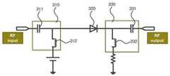
도 3에는 본 발명의 일 실시예에 따른 다이오드 블록의 상세 구조를 나타낸 회로도가 도시되어 있다. 도 3을 참조하면, 다이오드 블록(213)은 제1 매칭부(310), 쇼트키 다이오드(320) 및 제2 매칭부(330)를 포함하여 구성된다. 여기서, 제1 매칭부(310)는 쇼트키 다이오드(320) 전단에 배치되어 쇼트키 다이오드(320)와 연결되며, 제2 매칭부(330)는 쇼트키 다이오드(320) 후단에 배치되어 비선형 신호를 출력하기 위한 수단이다.3 is a circuit diagram showing a detailed structure of a diode block according to an embodiment of the present invention. Referring to FIG. 3, the
제1 매칭부(310) 및 제2 매칭부(320)는 양쪽에서 병렬로 유입되는 직류(DC) 바이어스가 유출되는 것을 방지하기 위한 DC 블록의 기능을 수행하는 캐패시터(311, 331) 및 교류(AC) 성분이 DC 블록에 유입되는 것을 방지하기 위한 인덕터(312, 332)를 포함하여 구성된다.The
쇼트키 다이오드 양단에 캐패시터(311, 331)이 배치되어 직류 바이어스를 다이오드에 공급할 수 있다.
쇼트키 다이오드 전단에 배치되는 제1 매칭부(310)의 인덕터(312)는 접지와 연결된다.The
제2 매칭부(330)는 제1 매칭부(310)와 같이 제2 캐패시터(331) 및 제2 인덕터(332)를 포함하여 구성된다. 다만, 제2 매칭부(330)에 포함된 제2 인덕터(332)는 저항과 연결된다.The
이와 같이, 다이오드 블록(213)은 쇼트키 다이오드(320) 전단 및 후단에 DC 바이어스를 쇼트키 다이오드에 공급하고 임피던스 매칭을 위한 매칭부(310, 330)를 구비하여 RF 신호에 상응하는 비선형 신호를 생성하여 출력할 수 있다.The
위상 조절부(214)는 다이오드 블록(213)을 통해 입력되는 비선형 신호에 대해 위상을 조절하기 위한 수단이다.The
예를 들어, 위상 조절부(214)는 제1 경로로 분배된 RF 신호와 위상차가 180도 차이가 나도록 비선형 신호의 위상을 조절하여 결합부(215)로 출력할 수 있다.For example, the
결합부(215)는 지연부(212)를 통해 지연된 RF 신호와 위상 조절부(214)를 통해 위상이 조절된 비선형 신호를 결합하여 전송부(220)로 출력한다.The combining
전송부(220)는 프리디스토터(210)를 통해 출력된 신호에 상응하는 광신호를 전송하기 위한 수단이다. 예를 들어, 전송부(220)는 LD(laser diode)를 포함할 수 있다.The
쇼트키 다이오드를 포함하는 프리디스토터(210)를 통해 LD의 비선형성을 보상하기 위해 쇼트키 다이오드를 이용하여 비선형 신호를 생성한 후 위상을 조절하여 LD 특성에 따른 비선형성을 보상할 수 있다.In order to compensate the nonlinearity of the LD through the
이와 같은 본 발명의 일 실시예에 따른 쇼트키 다이오드를 이용하여 비선형 신호를 생성하여 LD의 비선형성을 보상할 수 있는 광 송신기에 대해 우선 도 4에 도시된 바와 같이, 쇼트키 다이오드의 구조를 역방향 및 순방향으로 직렬로 구성한 다이오드 블록에 따른 비선형 신호의 그래프가 도 5에 도시되어 있다.As shown in FIG. 4, an optical transmitter capable of generating a nonlinear signal using a Schottky diode according to an embodiment of the present invention and compensating for nonlinearity of the LD will be described. The structure of the Schottky diode is reversed And a graph of a non-linear signal according to a diode block formed in series in the forward direction is shown in FIG.
도 4는 광송신기(200)의 다이오드 블록의 쇼트키 다이오드를 역방향 및 순방향 직렬로 배치한 구조로, 도 5에 도시된 바와 같이, 바이어스 전압에 따라 비선형 성분이 변화되는 것을 확인할 수 있으며, 위상 또한 변경되는 것을 알 수 있다.FIG. 4 shows a structure in which the Schottky diodes of the diode blocks of the optical transmitter 200 are arranged in the reverse direction and the forward direction. As shown in FIG. 5, it can be seen that the nonlinear component changes according to the bias voltage. Can be changed.
도 6은 본 발명의 다른 실시예에 따른 다이오드 블록의 쇼트키 다이오드를 순방향 및 역방향으로 병렬 구성한 다이오드 블록의 구조를 나타낸 것이며, 도 7은 도 6과 같이 쇼트키 다이오드를 병렬로 구성한 다이오드 구조에 따른 비선형 신호의 그래프이다.FIG. 6 shows a structure of a diode block in which a Schottky diode of a diode block according to another embodiment of the present invention is arranged in parallel in a forward direction and a reverse direction, and FIG. 7 shows a structure of a diode structure in which a Schottky diode is formed in parallel It is a graph of nonlinear signal.
도 7을 살펴보면, 도 5에서 설명한 바와 같이, 바이어스 전압에 따라 비선형 성분이 변화되고, 위상 또한 변경되는 것을 알 수 있다.Referring to FIG. 7, as described in FIG. 5, it can be seen that the non-linear component changes according to the bias voltage, and the phase also changes.
본 발명의 일 실시예에 따른 IM3 소거 기능을 갖는 선형 아날로그 광송신기(200)는 이와 같은 쇼트키 다이오드의 비선형적 특성을 이용하여 전송단의 LD의 비선형성을 보상할 수 있다.The linear analog optical transmitter 200 having the IM3 erase function according to an embodiment of the present invention can compensate the nonlinearity of the LD of the transmission end by using the nonlinear characteristic of the Schottky diode.
도 8의 810은 광송신기에서 RF를 딜레이만 시킨 후 광송신기(200)의 전송단을 거쳐 출력된 신호를 나타낸 그래프로, LD의 11.6 mA에서 비선형 성분인 IM3가 존재하는 것을 알 수 있다.8 is a graph showing a signal output from the optical transmitter through the transmission end of the optical transmitter 200 after delaying the RF in the optical transmitter. It can be seen that a nonlinear component IM3 exists at 11.6 mA of the LD.
도 8의 820은 본 발명의 일 실시예에 따른 다이오드 블록을 통해 비선형 신호를 생성한 후 위상을 조절하여 전송단을 통과한 후 비선형 성분인 IM3를 제거한 신호를 나타낸 그래프로, 쇼트키 다이오드를 통해 비선형 신호를 삽입한 후 위상 조절을 통해 전송한 후 이를 제거함으로써 광송신기(200)의 LD 특성에 따른 비선형 성분이 제거된 것을 알 수 있다.
8, 820 is a graph showing a signal obtained by removing a nonlinear component IM3 after passing through a transmission end by adjusting a phase after generating a nonlinear signal through a diode block according to an embodiment of the present invention. It can be seen that the nonlinear component according to the LD characteristic of the optical transmitter 200 is removed by transmitting the nonlinear signal through the phase adjustment and removing the nonlinear signal.
상기에서는 본 발명의 바람직한 실시예를 참조하여 설명하였지만, 해당 기술 분야에서 통상의 지식을 가진 자라면 하기의 특허 청구의 범위에 기재된 본 발명의 사상 및 영역으로부터 벗어나지 않는 범위 내에서 본 발명을 다양하게 수정 및 변경시킬 수 있음을 이해할 수 있을 것이다.It will be apparent to those skilled in the art that various modifications and variations can be made in the present invention without departing from the spirit or scope of the invention as defined in the appended claims. It will be understood that the invention may be varied and varied without departing from the scope of the invention.
210: 프리디스토터
220: 전송부210: predistorter
220:
Claims (9)
Translated fromKorean투톤(two-tone) RF 신호를 제1 경로 및 제2 경로로 분배하는 분배부;
상기 제1 경로의 RF 신호를 지연하는 지연부;
쇼트키 다이오드를 포함하며, 상기 쇼트키 다이오드를 이용하여 상기 제2 경로의 RF 신호를 입력받아 비선형 신호를 생성하는 다이오드 블록-상기 쇼트키 다이오드는 후단에 병렬로 저항과 연결됨;
상기 다이오드 블록으로부터 상기 비선형 신호를 입력받아 상기 제1 경로의 RF신호와의 위상차이가 180도 차이 나도록 상기 비선형 신호의 위상을 조절하는 위상 조절부; 및
상기 레이저 다이오드 전단에 결합되며, 상기 위상 조절부를 통해 위상 조절된 상기 비선형 신호와 상기 지연부를 통해 지연된 RF 신호를 결합하여 상기 레이저 다이오드의 비선형성을 보상하는 결합부를 포함하는 광송신기에 포함되는 프리디스토터.
A predistorter included in an optical transmitter and directly connected to a front end of a laser diode of the optical transmitter,
A distribution unit for distributing the two-tone RF signal to the first path and the second path;
A delay unit for delaying the RF signal of the first path;
A diode block including a Schottky diode and receiving the RF signal of the second path using the Schottky diode to generate a nonlinear signal, the Schottky diode being connected in parallel with a resistor in a subsequent stage;
A phase adjuster for receiving the nonlinear signal from the diode block and adjusting the phase of the nonlinear signal so that the phase difference from the RF signal of the first path is 180 degrees; And
And a coupling unit coupled to a front end of the laser diode and coupling the nonlinear signal phase-adjusted through the phase adjustment unit to an RF signal delayed through the delay unit to compensate for nonlinearity of the laser diode. foundation.
상기 다이오드 블록은 복수의 매칭부를 더 포함하되,
상기 매칭부는 상기 쇼트키 다이오드 전단 및 후단에 각각 연결되는 것을 특징으로 하는 광송신기에 포함되는 프리디스토터.The method according to claim 1,
The diode block may further include a plurality of matching units,
And the matching unit is connected to the front end and the rear end of the Schottky diode, respectively.
상기 매칭부는 병렬로 유입되는 직류(DC) 바이어스의 유출을 방지하기 위한 DC 블록 기능을 수행하는 캐패시터; 및
교류(AC) 성분이 상기 DC 블록으로 유입되는 것을 방지하는 인덕터를 포함하는 것을 특징으로 하는 광송신기에 포함되는 프리디스토터.The method of claim 3,
Wherein the matching unit includes: a capacitor that performs a DC blocking function to prevent leakage of DC bias introduced in parallel; And
And an inductor for preventing an AC component from flowing into the DC block.
상기 쇼트키 다이오드 전단에 배치되는 제1 매칭부의 인덕터는 접지와 연결되는 것을 특징으로 하는 광송신기에 포함되는 프리디스토터.5. The method of claim 4,
Wherein the inductor of the first matching unit disposed at the front end of the Schottky diode is connected to the ground.
상기 쇼트키 다이오드 후단에 배치되는 제2 매칭부의 인덕터는 저항과 연결되는 것을 특징으로 하는 광송신기에 포함되는 프리디스토터.5. The method of claim 4,
And the inductor of the second matching unit disposed at a rear end of the Schottky diode is connected to a resistor.
광신호를 출력하는 레이저 다이오드; 및
상기 레이저 다이오드 전단에 배치되고, 쇼트키 다이오드를 포함하고, 상기 쇼트키 다이오드를 이용하여 상기 레이저 다이오드의 비선형성을 보상하기 위한 비선형 신호를 생성하여 지연된 RF 신호와 결합하여 상기 레이저 다이오드로 출력하는 프리디스토터를 포함하되,
상기 프리디스토터는,
투톤(two-tone) RF 신호를 제1 경로 및 제2 경로로 분배하는 분배부;
상기 제1 경로의 RF 신호를 지연하는 지연부;
쇼트키 다이오드를 포함하며, 상기 쇼트키 다이오드를 이용하여 상기 제2 경로의 RF 신호를 입력받아 비선형 신호를 생성하는 다이오드 블록-상기 다이오드 블록은 상기 쇼트키 다이오드 후단에 병렬로 저항과 결합됨;
상기 다이오드 블록으로부터 상기 비선형 신호를 입력받아 상기 제1 경로의 RF신호와의 위상차이가 180도 차이나도록 상기 비선형 신호의 위상을 조절하는 위상 조절부; 및
상기 위상 조절부를 통해 위상 조절된 상기 비선형 신호와 상기 지연부를 통해 지연된 RF 신호를 결합하여 상기 레이저 다이오드의 비선형성을 보상하기 위한 결합된 RF 신호를 출력하는 결합부를 포함하는 것을 특징으로 하는 광송신기.
In an optical transmitter,
A laser diode for outputting an optical signal; And
A nonlinear signal for compensating the nonlinearity of the laser diode using the Schottky diode, and combining the nonlinear signal with a delayed RF signal to output the signal to the laser diode, Including a distortor,
The predistorter includes:
A distribution unit for distributing the two-tone RF signal to the first path and the second path;
A delay unit for delaying the RF signal of the first path;
A diode block including a Schottky diode and receiving the RF signal of the second path using the Schottky diode to generate a nonlinear signal, the diode block being coupled in parallel with a resistor after the Schottky diode;
A phase adjusting unit which receives the nonlinear signal from the diode block and adjusts the phase of the nonlinear signal so that the phase difference from the RF signal of the first path is 180 degrees; And
And a coupler for coupling the non-linear signal phase-adjusted through the phase adjuster and the RF signal delayed through the delay unit to output a combined RF signal for compensating non-linearity of the laser diode.
Priority Applications (1)
| Application Number | Priority Date | Filing Date | Title |
|---|---|---|---|
| KR1020130062815AKR101438355B1 (en) | 2013-05-31 | 2013-05-31 | Linear analog optical transmitter with IM3 cancellation function |
Applications Claiming Priority (1)
| Application Number | Priority Date | Filing Date | Title |
|---|---|---|---|
| KR1020130062815AKR101438355B1 (en) | 2013-05-31 | 2013-05-31 | Linear analog optical transmitter with IM3 cancellation function |
Publications (1)
| Publication Number | Publication Date |
|---|---|
| KR101438355B1true KR101438355B1 (en) | 2014-10-14 |
Family
ID=51995893
Family Applications (1)
| Application Number | Title | Priority Date | Filing Date |
|---|---|---|---|
| KR1020130062815AExpired - Fee RelatedKR101438355B1 (en) | 2013-05-31 | 2013-05-31 | Linear analog optical transmitter with IM3 cancellation function |
Country Status (1)
| Country | Link |
|---|---|
| KR (1) | KR101438355B1 (en) |
Cited By (1)
| Publication number | Priority date | Publication date | Assignee | Title |
|---|---|---|---|---|
| KR101816898B1 (en)* | 2015-12-22 | 2018-01-10 | 중앙대학교 산학협력단 | Linear analog optical transmitter having broadband based on schottky diode and predistorter included therein |
Citations (1)
| Publication number | Priority date | Publication date | Assignee | Title |
|---|---|---|---|---|
| KR20010045619A (en)* | 1999-11-05 | 2001-06-05 | 윤종용 | Apparatus for predistorting in wireless communication system |
- 2013
- 2013-05-31KRKR1020130062815Apatent/KR101438355B1/ennot_activeExpired - Fee Related
Patent Citations (1)
| Publication number | Priority date | Publication date | Assignee | Title |
|---|---|---|---|---|
| KR20010045619A (en)* | 1999-11-05 | 2001-06-05 | 윤종용 | Apparatus for predistorting in wireless communication system |
Non-Patent Citations (2)
| Title |
|---|
| 오규태. 쇼트키 다이오드를 이용한 전력증폭기용 프리디스토터에 관한 연구. 한국통신학회논문지, '02-10 Vol.27 No 10C, pp. 993-998, (2002.10.)* |
| 오규태. 쇼트키 다이오드를 이용한 전력증폭기용 프리디스토터에 관한 연구. 한국통신학회논문지, '02-10 Vol.27 No 10C, pp. 993-998, (2002.10.)* |
Cited By (1)
| Publication number | Priority date | Publication date | Assignee | Title |
|---|---|---|---|---|
| KR101816898B1 (en)* | 2015-12-22 | 2018-01-10 | 중앙대학교 산학협력단 | Linear analog optical transmitter having broadband based on schottky diode and predistorter included therein |
Similar Documents
| Publication | Publication Date | Title |
|---|---|---|
| KR102330688B1 (en) | Sequential broadband Doherty power amplifier having an adjustable output power backoff | |
| US10009138B2 (en) | Radio-over-fibre transmission in communications networks | |
| JP2004032412A (en) | Optical transmission system | |
| US10880008B2 (en) | Downstream node setup | |
| Han et al. | Linearity improvement of directly-modulated multi-IF-over-fibre LTE-A mobile fronthaul link using shunt diode predistorter | |
| US9143094B2 (en) | Microwave power amplification apparatus and method thereof | |
| KR102075813B1 (en) | Amplifier assembly | |
| KR101438355B1 (en) | Linear analog optical transmitter with IM3 cancellation function | |
| Goyal et al. | Single tone and multi tone microwave over fiber communication system using direct detection method | |
| CN112909734B (en) | High-speed laser driving circuit and high-speed laser system | |
| CN103548259A (en) | Wireless communications including distributed feedback architecture | |
| Kumar et al. | Performance evaluation of radio over fiber system by employing optical amplifiers EDFA AND SOA | |
| WO2008012865A1 (en) | Parent station device, child station device, and optical signal transmission system | |
| JP4568159B2 (en) | Bidirectional WDM optical analog transmission system | |
| Bogaert et al. | Narrowband photoreceiver for analog radio-over-fiber in the 24.25-29.5 GHz band | |
| Moutaly et al. | Performance of phase modulated RoF for 5G fronthaul uplink | |
| Yang et al. | A 28-nm CMOS EML Driver for 50G-PON Applications | |
| KR101816898B1 (en) | Linear analog optical transmitter having broadband based on schottky diode and predistorter included therein | |
| Chandan et al. | Performance Analysis of Radio over Fiber with WDM PON System | |
| Salleh et al. | Design the High Gain and Low Power Amplifier for Radio over Fiber Technology at 2.4 GHz | |
| Fernando | Radio over fiber in multimedia access networks | |
| US10135532B2 (en) | Optical receiver and method of receiving an optical communications signal | |
| Ismail et al. | Nonlinear distortion reduction in directly modulated semiconductor laser using feedforward linearisation | |
| KR100688605B1 (en) | Microwave Group Delay Timer Using Resonance Circuit | |
| Brandão | Development of a Remote Radio Unit and Optical Access Link for the ORCIP C-RAN Testbed |
Legal Events
| Date | Code | Title | Description |
|---|---|---|---|
| A201 | Request for examination | ||
| PA0109 | Patent application | St.27 status event code:A-0-1-A10-A12-nap-PA0109 | |
| PA0201 | Request for examination | St.27 status event code:A-1-2-D10-D11-exm-PA0201 | |
| N231 | Notification of change of applicant | ||
| PN2301 | Change of applicant | St.27 status event code:A-3-3-R10-R11-asn-PN2301 St.27 status event code:A-3-3-R10-R13-asn-PN2301 | |
| PN2301 | Change of applicant | St.27 status event code:A-3-3-R10-R11-asn-PN2301 St.27 status event code:A-3-3-R10-R13-asn-PN2301 | |
| D13-X000 | Search requested | St.27 status event code:A-1-2-D10-D13-srh-X000 | |
| D14-X000 | Search report completed | St.27 status event code:A-1-2-D10-D14-srh-X000 | |
| E902 | Notification of reason for refusal | ||
| PE0902 | Notice of grounds for rejection | St.27 status event code:A-1-2-D10-D21-exm-PE0902 | |
| E13-X000 | Pre-grant limitation requested | St.27 status event code:A-2-3-E10-E13-lim-X000 | |
| P11-X000 | Amendment of application requested | St.27 status event code:A-2-2-P10-P11-nap-X000 | |
| P13-X000 | Application amended | St.27 status event code:A-2-2-P10-P13-nap-X000 | |
| E701 | Decision to grant or registration of patent right | ||
| PE0701 | Decision of registration | St.27 status event code:A-1-2-D10-D22-exm-PE0701 | |
| GRNT | Written decision to grant | ||
| PR0701 | Registration of establishment | St.27 status event code:A-2-4-F10-F11-exm-PR0701 | |
| PR1002 | Payment of registration fee | Fee payment year number:1 St.27 status event code:A-2-2-U10-U11-oth-PR1002 | |
| PG1601 | Publication of registration | St.27 status event code:A-4-4-Q10-Q13-nap-PG1601 | |
| PN2301 | Change of applicant | St.27 status event code:A-5-5-R10-R11-asn-PN2301 St.27 status event code:A-5-5-R10-R13-asn-PN2301 | |
| P22-X000 | Classification modified | St.27 status event code:A-4-4-P10-P22-nap-X000 | |
| FPAY | Annual fee payment | Payment date:20170626 Year of fee payment:4 | |
| PR1001 | Payment of annual fee | Fee payment year number:4 St.27 status event code:A-4-4-U10-U11-oth-PR1001 | |
| FPAY | Annual fee payment | Payment date:20180625 Year of fee payment:5 | |
| PR1001 | Payment of annual fee | Fee payment year number:5 St.27 status event code:A-4-4-U10-U11-oth-PR1001 | |
| R18-X000 | Changes to party contact information recorded | St.27 status event code:A-5-5-R10-R18-oth-X000 | |
| PN2301 | Change of applicant | St.27 status event code:A-5-5-R10-R11-asn-PN2301 St.27 status event code:A-5-5-R10-R13-asn-PN2301 | |
| PN2301 | Change of applicant | St.27 status event code:A-5-5-R10-R11-asn-PN2301 St.27 status event code:A-5-5-R10-R13-asn-PN2301 | |
| FPAY | Annual fee payment | Payment date:20190807 Year of fee payment:6 | |
| PR1001 | Payment of annual fee | Fee payment year number:6 St.27 status event code:A-4-4-U10-U11-oth-PR1001 | |
| R18-X000 | Changes to party contact information recorded | St.27 status event code:A-5-5-R10-R18-oth-X000 | |
| PC1903 | Unpaid annual fee | Not in force date:20200831 Payment event data comment text:Termination Category : DEFAULT_OF_REGISTRATION_FEE St.27 status event code:A-4-4-U10-U13-oth-PC1903 | |
| PC1903 | Unpaid annual fee | Ip right cessation event data comment text:Termination Category : DEFAULT_OF_REGISTRATION_FEE Not in force date:20200831 St.27 status event code:N-4-6-H10-H13-oth-PC1903 | |
| PN2301 | Change of applicant | St.27 status event code:A-5-5-R10-R11-asn-PN2301 St.27 status event code:A-5-5-R10-R13-asn-PN2301 | |
| P22-X000 | Classification modified | St.27 status event code:A-4-4-P10-P22-nap-X000 | |
| R18-X000 | Changes to party contact information recorded | St.27 status event code:A-5-5-R10-R18-oth-X000 | |
| R18-X000 | Changes to party contact information recorded | St.27 status event code:A-5-5-R10-R18-oth-X000 |