KR101437193B1 - Micromirror actuator having encapsulation possibility and manufacturing method thereof - Google Patents
Micromirror actuator having encapsulation possibility and manufacturing method thereofDownload PDFInfo
- Publication number
- KR101437193B1 KR101437193B1KR1020097011120AKR20097011120AKR101437193B1KR 101437193 B1KR101437193 B1KR 101437193B1KR 1020097011120 AKR1020097011120 AKR 1020097011120AKR 20097011120 AKR20097011120 AKR 20097011120AKR 101437193 B1KR101437193 B1KR 101437193B1
- Authority
- KR
- South Korea
- Prior art keywords
- micro
- layers
- mirror
- actuator
- frame
- Prior art date
- Legal status (The legal status is an assumption and is not a legal conclusion. Google has not performed a legal analysis and makes no representation as to the accuracy of the status listed.)
- Active
Links
Images


Classifications
- G—PHYSICS
- G02—OPTICS
- G02B—OPTICAL ELEMENTS, SYSTEMS OR APPARATUS
- G02B26/00—Optical devices or arrangements for the control of light using movable or deformable optical elements
- G02B26/08—Optical devices or arrangements for the control of light using movable or deformable optical elements for controlling the direction of light
- G02B26/0816—Optical devices or arrangements for the control of light using movable or deformable optical elements for controlling the direction of light by means of one or more reflecting elements
- G02B26/0833—Optical devices or arrangements for the control of light using movable or deformable optical elements for controlling the direction of light by means of one or more reflecting elements the reflecting element being a micromechanical device, e.g. a MEMS mirror, DMD
- G02B26/0841—Optical devices or arrangements for the control of light using movable or deformable optical elements for controlling the direction of light by means of one or more reflecting elements the reflecting element being a micromechanical device, e.g. a MEMS mirror, DMD the reflecting element being moved or deformed by electrostatic means
- G—PHYSICS
- G02—OPTICS
- G02B—OPTICAL ELEMENTS, SYSTEMS OR APPARATUS
- G02B26/00—Optical devices or arrangements for the control of light using movable or deformable optical elements
- G02B26/08—Optical devices or arrangements for the control of light using movable or deformable optical elements for controlling the direction of light
- B—PERFORMING OPERATIONS; TRANSPORTING
- B81—MICROSTRUCTURAL TECHNOLOGY
- B81B—MICROSTRUCTURAL DEVICES OR SYSTEMS, e.g. MICROMECHANICAL DEVICES
- B81B3/00—Devices comprising flexible or deformable elements, e.g. comprising elastic tongues or membranes
- B—PERFORMING OPERATIONS; TRANSPORTING
- B81—MICROSTRUCTURAL TECHNOLOGY
- B81C—PROCESSES OR APPARATUS SPECIALLY ADAPTED FOR THE MANUFACTURE OR TREATMENT OF MICROSTRUCTURAL DEVICES OR SYSTEMS
- B81C1/00—Manufacture or treatment of devices or systems in or on a substrate
- B81C1/00015—Manufacture or treatment of devices or systems in or on a substrate for manufacturing microsystems
- B81C1/00134—Manufacture or treatment of devices or systems in or on a substrate for manufacturing microsystems comprising flexible or deformable structures
- B81C1/00166—Electrodes
- B—PERFORMING OPERATIONS; TRANSPORTING
- B81—MICROSTRUCTURAL TECHNOLOGY
- B81B—MICROSTRUCTURAL DEVICES OR SYSTEMS, e.g. MICROMECHANICAL DEVICES
- B81B2201/00—Specific applications of microelectromechanical systems
- B81B2201/03—Microengines and actuators
- B81B2201/033—Comb drives
- B—PERFORMING OPERATIONS; TRANSPORTING
- B81—MICROSTRUCTURAL TECHNOLOGY
- B81B—MICROSTRUCTURAL DEVICES OR SYSTEMS, e.g. MICROMECHANICAL DEVICES
- B81B2201/00—Specific applications of microelectromechanical systems
- B81B2201/04—Optical MEMS
- B81B2201/042—Micromirrors, not used as optical switches
Landscapes
- Engineering & Computer Science (AREA)
- Physics & Mathematics (AREA)
- Manufacturing & Machinery (AREA)
- Microelectronics & Electronic Packaging (AREA)
- General Physics & Mathematics (AREA)
- Optics & Photonics (AREA)
- Computer Hardware Design (AREA)
- Micromachines (AREA)
- Mechanical Light Control Or Optical Switches (AREA)
Abstract
Translated fromKoreanDescription
Translated fromKorean본 발명은, 내측 영역에, 하나 이상의 가동 마이크로-미러 소자 및 마이크로-미러 소자를 활성화하기 위한 다수의 핑거형 또는 콤형(comb-shaped) 전극들을 가지며, 상기 전극들은 높이에서 서로 오프셋되어 있고, 중간 층들을 통해 적어도 부분적으로 서로 전기적으로 절연되어 있는, 적어도 3개의 주요층들로 된 층 구조에 의해 형성되는, 마이크로-미러 액튜에이터, 및 그의 제조 방법에 관한 것이다.The present invention relates to a micromirror element comprising a plurality of finger-shaped or comb-shaped electrodes for activating at least one movable micro-mirror element and a micro-mirror element in the inner region, said electrodes being offset from each other at a height, The present invention relates to a micro-mirror actuator formed by a layer structure of at least three main layers which are at least partially electrically insulated from each other at least partially through layers, and to a method of manufacturing the same.
마이크로-전자기계 컴포넌트들(MEMS)은 수 많은 응용들에서 이용 가능하다. 이들의 예들은 가속 센서들, 속도 센서들, 또는 광 마이크로-센서들이다. 상기 MEMS 컴포넌트들 중 다수는, 컴포넌트의 내측 영역의 가동 구조에 의해 형성되는, 액튜에이터 또는 센서 소자의 샘플링 또는 활성화의 타입이 다르다. 본 발명은 상기 가동 마이크로-미러 소자가 다수의 전극들에 의해 샘플링 또는 활성화되는, 마이크로-미러 액튜에이터들에 관한 것이다. 이 경우의 응용의 특정 영역이 전자기적으로 구동되는 마이크로-스캐너 미러들로 나타내지고 있다.Micro-electromechanical components (MEMS) are available in many applications. Examples of these are acceleration sensors, velocity sensors, or optical micro-sensors. Many of the MEMS components differ in the type of sampling or activation of the actuator or sensor element, which is formed by the movable structure of the inner region of the component. The present invention relates to micro-mirror actuators in which the movable micro-mirror element is sampled or activated by a plurality of electrodes. A particular area of application in this case is represented by micro-scanner mirrors that are electromagnetically driven.
마이크로-스캐너 미러들은, 예컨대, 바코드 독출 장치들, 회로 기판 노광 유 닛, 레이저 스캐닝 마이크로스코프, 이미징 레이저 프로젝션, 또는 광 네트워크 스위치들에서 사용될 수 있다.Micro-scanner mirrors may be used, for example, in barcode reading devices, circuit board exposure units, laser scanning microscopes, imaging laser projection, or optical network switches.
콤형 또는 핑거형 전극들은, 보통의 구동 전압들에서도 액튜에이터 소자의 큰 편향을 허용하도록, 마이크로-스캐너 미러들의, 미러 플레이트들에 의해 형성된, 액튜에이터 소자들을 활성화하도록 부분적으로 사용된다. 인터메싱(intermeshing) 콤형 전극들의 장점은, 이동 중에도, 동일하게 작은 전극 스페이스를 갖는 큰 전극 표면으로 인해 전기적 용량이 증가되는 점이다. 원칙적으로, 콤 전극 구동부들은 기판 상에 배치된 고정 전극 콤 및 액튜에이터 소자에 부착된, 인터메시된, 가동 전극 콤을 포함한다. 액튜에이터 소자의 편향은, 일부 실시예들에서, 전극들이 동일 평면에 있을 때, 전극 구조의 제조-관련 비대칭들이 인터메시 전극 콤들 상의, 전체적으로 동일하지 않은, 전계들을 발생시키는 점에서 이루어지게 된다. 그의 공진 주파수에서 액튜에이터 소자가 여자되면, 초기의 매우 작은 편향들이 몇도의 큰 진폭들로 증대된다. 이 원리의 단점은 이러한 타입의 미러 액튜에이터 만이 그의 공진 주파수에서 유용하게 큰 편향들을 나타내며 따라서 그의 가능한 용도가 크게 제한되는 점이다. 또한, 선택적인 방향의 부족 때문에 일시적인 진동 절차가 독특하게 정의되지 않게 됨으로써, 액튜에이터 소자가 다른 방향들로 진동할 수 있다. 따라서, 그의 여자 신호에 대한 액튜에이터 소자의 위상 위치는 특정되지 않고 180°까지 변화할 수 있다.Comb-shaped or finger-shaped electrodes are used to partially activate the actuator elements, formed by the mirror plates, of the micro-scanner mirrors to allow large deflection of the actuator elements even at normal drive voltages. The advantage of intermeshing comb-shaped electrodes is that, even on the move, the electrical capacity is increased due to the large electrode surface with the same small electrode space. In principle, the comb electrode drivers include an intermeshed, movable electrode comb attached to the fixed electrode comb and actuator elements disposed on the substrate. The deflection of the actuator element is, in some embodiments, made when the electrodes are in the same plane, in that the fabrication-related asymmetries of the electrode structure generate electric fields that are not totally the same on the intermeshing electrode combs. When the actuator element is excited at its resonant frequency, the initial very small deflections are amplified with large amplitudes of several degrees. A disadvantage of this principle is that only this type of mirror actuator exhibits large deflections usefully at its resonant frequency and therefore its possible applications are severely limited. Also, due to the lack of selective orientation, the temporary vibration procedure is not uniquely defined, so that the actuator element can vibrate in different directions. Thus, the phase position of the actuator element with respect to its excitation signal is not specified and can vary up to 180 degrees.
이 문제들을 피하도록, 콤 전극들은 정적 및 가동 전극 콤들이 상호 높이 오프셋을 갖는 채로 사용된다. 이러한 타입의 형태를 이용하면, 콤 전극들의 높이 오 프셋에 의해 정해지는, 액튜에이터 소자의 경사 범위 내의 소정 각도를 설정할 수 있다. 따라서, 공진 동작에 더하여, 준-정적 동작도 적어도 공진 주파수 아래의 주파수들에서 가능하게 된다.To avoid these problems, the comb electrodes are used with the static and movable electrode combs having mutual height offset. With this type of configuration, a predetermined angle within the range of inclination of the actuator element, which is determined by the height offset of the comb electrodes, can be set. Thus, in addition to resonant operation, quasi-static operation is also possible at least at frequencies below the resonant frequency.
중간 층들을 통해 적어도 부분적으로 서로 전기적으로 절연되어 있는, 적어도 3개의 주요층들로 된 층 구조가 생성되는, 이러한 타입의 마이크로-액튜에이터 제조 방법이, 2005년 10월, 마이크로-전자기계 시스템 저널, 볼륨 14, 이슈 5, 페이지 1144 내지 1155에 기재된, 소형 자체-정렬 핑거 갭들을 갖는 고 종횡비 버티컬 콤보-드라이브 액튜에이터가, 이. 티. 칼렌 등의 공보에 알려져 있다. 이 층들은, 높이가 서로 오프셋된, 액튜에이터 소자 및 콤형 활성 전극들을 형성하도록 설계되어 구조화된다.This type of micro-actuator fabrication method, wherein a layer structure of at least three major layers is created, at least partially electrically isolated from each other through the intermediate layers, is disclosed in the Micro-Electro Mechanical Systems Journal, Volume 14, Issue 5, pages 1144-1155, high aspect ratio vertical combo-drive actuators having miniature self-alignment finger gaps. tea. Karlen et al. These layers are designed and structured to form actuator elements and comb-like active electrodes whose heights are offset from each other.
상기한 마이크로-스캐너 미러 등의, 마이크로-전자기계 컴포넌트들을 제조하도록, 가동 구조물들, 즉 가동 액튜에이터 또는 센서 소자들,의 보호가 제조 과정 중에도 필요하게 된다. 특히 분리 과정 중에, 서로 인접한 프로세스 콤포넌트들을 갖는 웨이퍼는 개별 액튜에이터 칩들로 절단되며, 아직 캡슐화되지 않은 컴포넌트들의 소잉(sawing) 과정으로 인해 물 및 톱밥에서의 오염이 발생된다. 이 오염은 전기적인 단락을 매우 신속하게 하거나 또는 마이크로미터-미세 구동 콤 구조들의 기계적 봉쇄를 야기할 수 있다. 다수의 마이크로-스캐너 미러들이 에치백 트렌치를 갖기 때문에, 특히, 실제 액튜에이터 구조는 단지 수십 마이크로미터 두께이지만 동시에 신장되면 멀티플 밀리미터로 되는, 다이어프램을 나타내며, 또한 상기 컴포넌트 또는 칩은 비캡슐화된 상태에서 기계적으로 매우 취약하다. 따라서, 소위 웨 이퍼 레벨 패키징을 통해서만 고수율이 가능하며, 가동 센서 또는 액튜에이터 소자 및 전극들이 배치된, 컴포넌트의 내측 영역은 분리 전에 웨이퍼 상에서 밀폐되어 밀봉된 채 폐쇄된다. 이 방식으로, 상기 컴포넌트는 크게 변화하는 환경 조건들(온도, 압력, 대기중 습도) 하에서 균일한 전자-기계적 거동을 갖게 된다.In order to manufacture micro-electromechanical components, such as the micro-scanner mirrors described above, protection of movable structures, i. E. Movable actuators or sensor elements, is also required during manufacture. Particularly during the separation process, wafers with process components that are adjacent to each other are cut into individual actuator chips, and contamination of water and sawdust is caused by the sawing process of the components that have not yet been encapsulated. This contamination can cause electrical shorting very quickly or mechanical blocking of micrometer-fine drive comb structures. In particular, since the micro-scanner mirrors have etchback trenches, the actual actuator structure represents a diaphragm that is only a few tens of micrometers thick, but multiple millimeters at the same time, and the component or chip is mechanically . Thus, a high yield is only possible through so-called wiper-level packaging, and the inner area of the component, in which the movable sensor or actuator elements and electrodes are disposed, is sealed closed on the wafer prior to separation and closed. In this way, the component has a uniform electro-mechanical behavior under largely changing environmental conditions (temperature, pressure, atmospheric humidity).
마이크로-스캐너 미러들에 대해 현재까지 알려진 많은 제조 프로세스들은, 외측에서 전극들과 콘택팅하는 문제들이 지금까지 비제한적인 캡슐화를 허용하지 않았기 때문에, 밀폐되어 밀봉된 캡슐을 얻기 위해, 양극 또는 공융 웨이퍼 접합에 기초한, 프로세스와 매우 제한적인 방식으로 또는 전혀 통일화되어 있지 않다.Many fabrication processes known to date for micro-scanner mirrors have shown that the problems of contacting external electrodes with electrodes have so far not allowed non-limiting encapsulation, so that in order to obtain a hermetically sealed capsule, Based on bonding, in a very limited manner with the process or not at all.
따라서, 정전기적으로 구동되는 단축 마이크로-스캐너 미러의 활성화는 가장 간단한 경우에, 캡슐 외측의 단자들을 통해 인가된 후에 밀폐되어 밀봉된 캡슐로 인도되어야 하는, 두 개의 다른 포텐셜들을 필요로 한다. 이는, 제조 프로세스가 서로 수직으로 놓여있고 서로 절연된 두 개의 전도성 액튜에이터 층들을 제공하면, 가능해진다. 따라서, 제조된 단축 미러는 DC 전압의 인가에 따라 일측 상에서 준 정적으로 변형되거나 또는 적절한 AC 전압을 이용하여 공진을 야기할 수 있다. 그러나, 예컨대, 일측에서 뿐만 아니라, 양측에서 준 정적으로 단축 미러를 편향시킬 수 있도록, 한 쌍 이상의 콤 전극이 활성화를 위해 사용되는 경우, 서로 절연된 3개의 포텐셜들이 요구되며, 그중 적어도 둘은 서로 측면으로 절연되고 공간적으로 분리되어 있어야 한다. 지금까지 알려진 상기 제조 방법들은 이러한 목적으로 포텐셜을 공간적 및 전기적으로 서로 분리된 영역들로 전도하는 최상부층을 다음 절연 층에 대해 트렌치 다운 에칭함에 의해 분할한다. 그러나, 이 트렌치들은 항상 캡슐 화된 내부 및 외부 사이의 가스 교환을 허용하기 때문에, 상기 트렌치들이 밀봉 웨이퍼 레벨 패키징을 방해하는 전기적 분리에 대해 필요하게 된다. 캡슐화를 위해 양극 접합 방법을 이용하는 경우, 상기 접합은 트렌치 위치에서 차단된다. 공융 접합의 경우, 서로 절연된 인쇄 도체들의 단락도 발생된다. 상기 조건들은 단축 미러가 아니라 2축 마이크로-스캐너 미러가 제조되는 경우, 공간적으로 분리된 또 다른 포텐셜들이 전자에 추가되어야 하기 때문에, 상당히 더 복잡해질 것이다.Thus, the activation of an electrostatically actuated uniaxial micro-scanner mirror requires two different potentials, which, in the simplest case, must be applied through the outside terminals of the capsule and then introduced into the sealed capsule. This is possible if the manufacturing process is to provide two conductive actuator layers that are placed perpendicular to each other and insulated from each other. Therefore, the manufactured uniaxial mirror may be quasi-statically deformed on one side according to the application of the DC voltage, or may cause resonance using an appropriate AC voltage. However, for example, when one or more comb electrodes are used for activation so that the uniaxial mirror can be deflected quasi-static not only on one side but also on both sides, three potentials insulated from each other are required, It should be insulated laterally and spatially separated. The above-described fabrication methods known for this purpose divide the top layer that conducts potentials into spatially and electrically isolated regions to each other by trench-down etching the next insulating layer. However, because these trenches always allow gas exchange between the encapsulated interior and exterior, the trenches are required for electrical isolation that hinders sealed wafer level packaging. If an anodic bonding method is used for encapsulation, the bonding is cut off at the trench location. In the case of eutectic bonding, a short circuit of printed conductors insulated from each other also occurs. The above conditions will be significantly more complicated because, if a two-axis micro-scanner mirror is made, rather than a single axis mirror, another spatially separated potential must be added to the electron.
MEMS 컴포넌트들에 대한 웨이퍼 레벨 패키징 방법이 미국 특허 제6,146,917호에 알려져 있으며, 공동들이 제공된 실리콘 또는 글라스 웨이퍼가, 밀봉 캡슐을 얻도록, 공융 접합 또는 양극 접합에 의해 MEMS 웨이퍼에 접합되어 있다. 제조 프로세스 중에, 컴포넌트를 둘러싸는, 커버 소자에 밀폐되어 밀봉된 연결을 위해 요구되는 플래너리티(planarity)를 가진, 폐쇄된 접합 영역이 웨이퍼에 의해 형성된 최하부층 상에 분명하게 유지되어야 한다. 상기 커버 소자는 상기 주위의 접합 영역의 지점들에 적절한 웹들을 가진, 공동들이 제공된 실리콘 또는 글라스 웨이퍼이다. 캡슐화된 MEMS 컴포넌트의 전극들의 외부측으로의 전기적 접속은, 외부측으로부터 MEMS 컴포넌트의 캡슐화된 내측 영역으로 측면으로 인도하는, 웨이퍼에 임플란트된 도체 라인들에 의해 실행된다.A wafer level packaging method for MEMS components is known from U.S. Patent No. 6,146,917, wherein silicon or glass wafers provided with cavities are bonded to a MEMS wafer by eutectic bonding or anodic bonding to obtain a sealing capsule. During the manufacturing process, the closed junction area, with the planarity required for the sealed connection sealed to the cover element surrounding the component, must be clearly maintained on the lowermost layer formed by the wafer. The cover element is a silicon or glass wafer provided with cavities, with suitable webs at the points of the surrounding bonding region. The electrical connection to the outside of the electrodes of the encapsulated MEMS component is carried out by conductor lines implanted in the wafer, leading sideways from the outside to the encapsulated inner region of the MEMS component.
본 발명의 목적은, 하나 이상의 가동 마이크로-미러 소자, 및 높이에서 서로 오프셋되어 있는, 다수의 핑거형 또는 콤형 전극들을 가지는 마이크로-미러 액튜에이터를 제조하기 위한 방법을 제공하는 것이며, 상기 방법은 간단한 방식으로 웨이퍼 레벨 상에서의 액튜에이터의 내측 영역의 밀폐되어 밀봉된 캡슐화를 허용한다. 또한, 대응하게 구조화된 마이크로-미러 액튜에이터가 본 발명에 의해 제공된다.It is an object of the present invention to provide a method for manufacturing a micro-mirror actuator having one or more movable micro-mirror elements and a plurality of finger-shaped or comb-shaped electrodes offset from each other in height, Sealed encapsulation of the inner region of the actuator on the wafer level. In addition, correspondingly structured micro-mirror actuators are provided by the present invention.
상기 목적은 청구항1 및 8에 따른 방법 및 마이크로-미러 액튜에이터에 의해 실현된다. 상기 액튜에이터 및 방법들의 유익한 실시예들이 이하의 설명 및 예시적인 실시예들로부터 추론될 수 있는 하위크레임들의 주된 내용이다.This object is achieved by the method according to
본 발명의 방법에서, 적어도 3개의 주요층들, 바람직하게는 중간 층들을 통해 적어도 부분적으로 전기적으로 서로 절연된 반도체 층들로 된, 층 구조가 생성된다. 상기 층들은 마이크로-미러 소자 및 전극들을 형성하도록 설계되어 구조화된다. 상기 제안된 방법에서, 층들의 구조화는, 적어도, 액튜에이터의 내측 영역을 둘러싸고 프레임 상으로의 커버 플레이트의 부착에 의해 내측 영역의 밀봉 캡슐화를 허용하는, 상부 주 층으로부터 폐쇄된(고체) 프레임이 얻어지는 방식으로 실행된다. 상기 프레임의 상부 측의 표면, 즉 프레임의 최상부층의 표면은, 커버 플레이트의 밀폐되어 밀봉된 부착을 위해 필요한 플래너리티가 아직 충분하지 않은 경우, 상기 구조화 후에 그 목적을 위해 적절하게 연마된다. 또한, 본 발명의 방법에서, 층 구조화의 생성 중에, 상기 층들 중 적어도 두 개 사이에, 중간 층들을 통해 상기 층들로부터 전기적으로 절연된, 도체 레벨이 생성되어 도체 라인들 또는 패스들을 형성하도록 구조화된다. 상기 구조화는 하나 이상의 전극들이 컴포넌트의 제조 중에 하나 이상의 중간 층들에 콘택트 구멍들을 형성한 후에 상기 도체 패스들을 통해 프레임의 외측에 전기적으로 콘택트되는 방식으로 실행된다. 이 경우 상기 전극들은, 그 사이에 도체 레벨이 생성된, 적어도 두 개의 주요층들에 의해 형성된다. 따라서, 프레임 및/또는 캡슐 외측과 전극들의 콘택팅은, 캡슐화를 위해 필요한 캡슐화 용 연결면들의 평면 재질을 손상시키지 않고, 매립된 상기 도체 패스들에 의해 실현된다. 따라서, 상기 방법은, 바람직하게 프레임에 커버 플레이트를 접합하도록 양극 또는 공융 웨이퍼 접합을 이용하는, 간단한 방식으로 밀폐되어 밀봉된 캡슐을 제조할 수 있도록 허용한다. 상기 두 개의 접합 방법들 대신에, 예컨대, 글라스 플릿 접합 등의, 다른 접합 기술들도 상기 접합을 생성하도록 사용될 수 있다.In the method of the present invention, a layer structure is formed of at least three major layers, preferably semiconductor layers, at least partially electrically insulated from each other through the intermediate layers. The layers are designed and structured to form micro-mirror elements and electrodes. In the proposed method, the structuring of the layers results in at least a closed (solid) frame being obtained from the upper main layer, which allows encapsulation of the inner region by encapsulation of the cover plate on the frame, surrounding the inner region of the actuator . The surface on the top side of the frame, i.e. the surface of the top layer of the frame, is suitably polished for that purpose after the structuring if the planarity required for the closed and sealed attachment of the cover plate is not yet sufficient. Further, in the method of the present invention, a conductor level, which is electrically insulated from the layers via intermediate layers, is created between at least two of the layers during formation of the layer structure to form conductor lines or passes . The structuring is performed in such a way that one or more electrodes are electrically contacted to the outside of the frame through the conductive paths after forming contact holes in one or more intermediate layers during the manufacture of the component. In this case, the electrodes are formed by at least two main layers, in which a conductor level is created. Thus, the contact of the frame and / or outside of the capsule with the electrodes is realized by the buried conductor paths without damaging the planar material of the encapsulation connection surfaces necessary for encapsulation. The method thus permits the production of a hermetically sealed capsule in a simple manner, preferably using positive or eutectic wafer bonding to bond the cover plate to the frame. Instead of the two joining methods, other joining techniques, such as, for example, glass frit joining, can also be used to create the joining.
상기 제안된 방법에서, 캡슐화는 웨이퍼 레벨 상에 미리 실행될 수 있고, 그 후 웨이퍼 사이즈의 다른 웨이퍼 또는 기판이 상기 층 구조 상의 커버 플레이트로서 부착되어 웨이퍼 상에 서로 인접하게 배치된 마이크로-미러 액튜에이터들의 프레임들에 밀폐되어 밀봉된 채 접합된다. 또한, 상기 커버 플레이트는, 그 커버 플레이트에 의해 마이크로-미러 소자들의 이동 자유도를 손상시키지 않도록, 알려진 방식으로 공동들을 가질 수 있다. 이하 컴포넌트라고도 하는, 상기 액튜에이터가 최하부 주 층을 통한 통과 구멍을 가지는 경우, 부가적인 바닥 커버도 밀폐되어 밀봉된 캡슐화를 위해 제공될 수 있다. 이는, 상기 최하부 주 층이 일반적으로, 바닥 플레이트로서 다른 웨이퍼 또는 기판에 접합되도록 그의 하부측이 충분한 플래너리티를 갖는 웨이퍼를 포함하기 때문에, 문제로 되지 않는다.In the proposed method, the encapsulation can be performed beforehand on the wafer level, and then another wafer or substrate of wafer size is attached as a cover plate on the layer structure to form a frame of micro-mirror actuators And are hermetically sealed and sealed to each other. The cover plate may also have cavities in a known manner so as not to impair the freedom of movement of the micro-mirror elements by the cover plate. If the actuator has a through-hole through the lowermost main layer, also referred to hereinafter as a component, an additional bottom cover may also be provided for sealing and encapsulating encapsulation. This is not a problem since the lowermost main layer generally includes a wafer whose lower side has sufficient planarity such that it is bonded to another wafer or substrate as a bottom plate.
광학적 응용들을 위해 마이크로-스캐너 미러 또는 다른 MEMS 컴포넌트를 제조하는 중에, 예컨대 글라스 등의, 적어도 하나의 광 파장 대역에서 투명한 재료로부터 커버 플레이트, 및 선택적으로 필요하게 되는 바닥 플레이트를 선택할 필요가 있다. 그러나, 이는 본 발명의 방법에서 문제를 야기하지 않는다.During the manufacture of micro-scanner mirrors or other MEMS components for optical applications, there is a need to select a cover plate, and optionally a bottom plate, that is required from transparent materials, such as glass, in at least one optical wavelength band. However, this does not cause problems in the method of the present invention.
여기에서 제안된 제조 프로세스는 항상, 마이크로-미러 소자 및 전극들을 갖는 내부 영역 둘레에서, 완전 폐쇄되고, 그의 최상부는, 최상부 액튜에이터 (주) 층이 제조되는 것과, 동일한 층으로부터 제조되는, 연마 또는 토포그래피-프리 프레임을 제공한다. 그럼에도 불구하고 캡슐 내로 서로 분리되어 있는 거의 임의의 수의 포텐셜들을 리드하도록, 상기 제안된 제조 프로세스는 또한, 예컨대 미러 플레이트, 또는 마이크로-미러 소자들, 스프링 서스펜션들, 및 높이-오프셋을 갖는 전극 콤 구조물들에 대해 사용될 수 있는, 두 개의 두꺼운 전기 전도성 액튜에이터들에 추가하여, 증착된 도체 레벨을 포함한다. 이 도체 레벨은 하부 액튜에이터 층 위에 배치됨이 바람직하지만, 그에 대해 전기적으로 절연되어야 하고, 상부 액튜에이터 층 아래에서도, 그에 대해 전기적으로 절연되어 있다. 트렌치들에 의해 서로 절연되고, 내부 영역의 내측에 배치된, 상부 액튜에이터 층의 아일랜드들은 상기 도체 레벨을 통해 콘택트될 수 있다. 이 목적으로, 적절한 개별 도체 패스들로 구조화된 상기 도체 레벨로, 상부 액튜에이터 층 아래에 배치된, 상기 절연층에 콘택트 홀들이 미리 형성되며, 상기 패스들을 통해 도체 패스들 및 상부 액튜에이터 층의 절연된 아일랜드들 사이의 전기 접속이 이루어진다.The manufacturing process proposed here is always completely closed around the inner region with the micro-mirror element and the electrodes, and the top of it is made up of the top actuator layer, And provides a graphics-free frame. Nevertheless, the proposed fabrication process can also be used to lead, for example, to a mirror plate, or micro-mirror elements, spring suspensions, and electrode combs having height- In addition to two thick electrically conductive actuators, which may be used for structures, include a deposited conductor level. This conductor level is preferably disposed above the lower actuator layer, but it must be electrically insulated therefrom and is electrically insulated therefrom even under the upper actuator layer. The islands of the upper actuator layer, which are insulated from each other by trenches and disposed inside the inner region, can be contacted through the conductor level. For this purpose, at the conductor level structured with suitable individual conductor paths, contact holes are preformed in the insulating layer, disposed below the upper actuator layer, through which the conductor paths and the insulated < RTI ID = 0.0 > Electrical connections between the islands are made.
상기 제안된 제조 프로세스는 서로 높이에서 오프셋을 가진 콤 전극들의 생성을 허용한다. 이들 높이-오프셋을 갖는 콤 전극들은 공진 동작 뿐만 아니라, 전자기적으로 구동되는 마이크로-미러 소자의 준 정적의 동작도 허용한다. 상기 설명된 제조 시퀀스는 적어도 3개의 다른 층 두께로 가동 액튜에이터 구조들을 생성할 수 있는 가능성을 제공한다. 따라서, 마이크로-미러 소자의 서스펜션에 대한 토션 스프링은 필요에 따라 최소 층 두께로 제조될 수 있는 한편, 구동 및/또는 활성화를 위한 콤 전극들은 적절한 층 두께에서 생성될 수 있고, 마이크로-미러 소자는 필요에 따라 3개의 적용 가능한 층 두께 중 하나로 제조될 수 있다. 매우 작은 미러 직경(<0.5mm)의 마이크로-스캐너 미러는 미리 작은 층 두께로 처리될 수 있지만, 정적 변형은 에지 길이의 제곱의 스케일로 되고 동적 변형은 미러의 에지 길이의 5승의 스케일로 되기 때문에, 중간 및 큰 미러 직경들(멀티플 밀리미터까지)은 대응하게 큰 층 두께를 필요로 한다. 단지 수십 마이크로미터 두께인 미러들에 더하여, 상기 제안된 제조 프로세스는 또한, 예컨대, 웨이퍼 두께가, 수백 마이크로미터 두께까지인 미러의 제조도 허용할 수 있다. 상기 구조화를 위한 포토마스크들의 설계만으로 특정 액튜에이터 구조의 두께를 결정한다. 상기 제조 시퀀스는 항상 변함없이 동일하게 된다.The proposed fabrication process allows the creation of comb electrodes with offset in height from one another. The comb electrodes having these height-offsets allow not only the resonant operation, but also quasi-static operation of the electromagnetically driven micro-mirror element. The manufacturing sequence described above provides the possibility to create movable actuator structures with at least three different layer thicknesses. Thus, the torsion springs for the suspension of the micro-mirror elements can be manufactured with a minimum layer thickness as required, while comb electrodes for driving and / or activating can be produced with the appropriate layer thickness, and the micro- And may be manufactured to one of three applicable layer thicknesses as required. A micro-scanner mirror of very small mirror diameter (< 0.5 mm) can be processed with a small layer thickness in advance, but the static deformation becomes the scale of the square of the edge length and the dynamic deformation becomes the scale of the fifth power of the edge length of the mirror Therefore, medium and large mirror diameters (up to multiple millimeters) require a correspondingly large layer thickness. In addition to mirrors that are only a few tens of micrometers thick, the proposed fabrication process may also allow the fabrication of mirrors, for example, wafer thicknesses up to several hundred micrometers thick. The thickness of the particular actuator structure is determined only by designing the photomasks for the structuring. The manufacturing sequence is always the same.
본 특허 출원에서 설명된 제조 시퀀스에서, 양극 또는 공융 접합 등의 고온 웨이퍼 접합 방법들이 액튜에이터를 손상시키지 않고 사용될 수 있음으로써, 고온-내성 재료들만이 바람직하게 사용된다. 도체 패스들이 구동 전극들과 동일 층으로부터 제조되는 제조 프로세스들에 대비하여, 여기에서 제공된 은폐 또는 매립된 도체 레벨을 이용하면, 액튜에이터가 웨이퍼 레벨 패키지에 의해 밀봉되어 밀봉된 채 패키지된 경우에도 서로 절연된 액튜에이터의 임의의 수의 영역들이 콘택트될 수 있다.In the manufacturing sequence described in the present patent application, only high temperature-resistant materials are preferably used because high temperature wafer bonding methods such as anodic or eutectic bonding can be used without damaging the actuators. Even if the actuators are packaged sealed and sealed by a wafer-level package, the use of the concealed or buried conductor levels provided herein, as opposed to manufacturing processes in which conductor paths are made from the same layer as the drive electrodes, Any number of regions of the actuated actuator can be contacted.
상기 방법을 이용하여 제조된 마이크로-미러 액튜에이터는 내측 영역에 적어도 하나의 가동 마이크로-미러 소자, 및 상기 마이크로-미러 소자를 활성화시키도록, 높이에 오프셋을 가진, 다수의 콤형 또는 핑거형 전극들을 가진다. 상기 컴포넌트는 중간 층들을 통해 적어도 부분적으로 서로 전기적으로 절연된, 적어도 3개의 주요층들로 된 층 구조로부터 형성된다. 상기 내측 영역은, 커버 플레이트를 프레임에 부착함에 의해 내측 영역의 밀봉 캡슐화를 허용하는, 적어도 상부 주 층으로부터 형성되는, 폐쇄된 프레임에 의해 둘러싸인다. 상기 층들 중 적어도 둘 사이에, 도체 패스들을 가진, 중간 층들을 통해 상기 층들로부터 전기적으로 절연된, 도체 레벨이 배치되며, 그 패스들을 통해 하나 이상의 전극들이 중간 층들의 콘택트 구멍들을 통해 프레임 외측과 전기적으로 콘택트될 수 있다. 상기 마이크로-미러 액튜에이터는 정전기적으로 구동되는 단축 또는 다축 마이크로-미러를 가진 마이크로-스캐너 미러이다.The micro-mirror actuator fabricated using the method has at least one movable micro-mirror element in the inner region and a plurality of comb-shaped or finger-shaped electrodes with an offset in height to activate the micro-mirror element . The component is formed from a layer structure of at least three major layers that are at least partially electrically insulated from one another through the intermediate layers. The inner region is surrounded by a closed frame, formed from at least the upper main layer, which allows sealing encapsulation of the inner region by attaching the cover plate to the frame. A conductor level is disposed between the at least two of the layers, the conductor levels being electrically insulated from the layers through intermediate layers, with conductor paths, through which the one or more electrodes are electrically connected to the outside of the frame through the contact holes of the middle layers, . ≪ / RTI > The micro-mirror actuator is a micro-scanner mirror having an electrostatically driven short axis or multi-axis micro-mirror.
상기 제안된 방법 및 연관된 마이크로-미러 액튜에이터는 도면들과 연계하여 예시적인 실시예들을 기초로 이하에서 다시 한번 더욱 상세하게 설명된다. 도면들에서 :The proposed method and the associated micro-mirror actuator are described in further detail below in more detail on the basis of illustrative embodiments in conjunction with the drawings. In the drawings:
도1a 내지 도1g는 상기 제안된 제조 방법의 제1 예를 나타낸 도면,1A to 1G are views showing a first example of the proposed manufacturing method,
도2a 내지 도2g는 상기 제안된 제조 방법의 제2 예를 나타낸 도면,2A to 2G are views showing a second example of the proposed manufacturing method,
도3은 본 발명의 방법에 따라 얻어질 수 있는 이축 마이크로-스캐너 미러의 평면도,Figure 3 is a top view of a biaxial micro-scanner mirror that may be obtained according to the method of the present invention,
도4는 콤 전극들의 높이 오프셋 및 활성화의 예를 나타낸 도면,4 shows an example of height offset and activation of comb electrodes,
도5는 콤 전극들의 높이 오프셋 및 형태의 제2 예를 나타낸 도면,5 shows a second example of height offset and shape of comb electrodes,
도6은 콤 전극들의 높이 오프셋 및 형태의 제3 예를 나타낸 도면, 및6 shows a third example of height offset and shape of comb electrodes, and
도7은 상기 제안된 마이크로-미러 액튜에이터의 캡슐화의 예를 나타낸 도면이다.7 is a view showing an example of encapsulation of the proposed micro-mirror actuator.
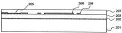
상기 제시된 방법은, 마이크로-스캐너 미러가 실리콘 기술로 제조되는, 예시적인 실시예를 기초로 이하에서 설명된다. 상기 방법의 개별적인 단계들은 도1a 내지 도1g를 참조하여 파악될 수 있다. 실리콘 웨이퍼(101)는, 예컨대, 1μm 두께의 SiO2 층(102)으로 열산화 공정에 의해 코팅된, 기판 재료로서 사용된다. 예컨대 30μm 두께의 비교적 두꺼운 폴리실리콘 층(103)이 제1 절연층으로서 사용된 상기 (중간) 층에 에피택시 증착 공정에 의해 인가된다. 에피택시 증착 공정에 의해 인가된 이러한 타입의 폴리실리콘 층들은 또한 이하 에피폴리 층들이라고도 한다.The method presented above is described below based on an exemplary embodiment in which the micro-scanner mirror is fabricated with silicon technology. The individual steps of the method can be understood with reference to Figures 1A-Ig. The
그 후 상기 웨이퍼는 화학-기계적 연마(CMP)에 의해 평탄화된다. 이 경우, 도2a 내지 도2g에서와 같이, 도1a 내지 도1g에서는, 하나의 마이크로-스캐너 미러가 생성된, 웨이퍼의 작은 부분만을 나타내고 있다. 매우 많은 이러한 타입의 마이크로-스캐너 미러들은 층 구조화에 의해 전체 웨이퍼 상에 알려진 방식으로 동시에 서로 인접하게 빌드 업된다.The wafer is then planarized by chemical-mechanical polishing (CMP). In this case, as shown in Figs. 2A to 2G, Figs. 1A to 1G show only a small portion of the wafer where one micro-scanner mirror is generated. Much of this type of micro-scanner mirrors are built up adjacent to one another simultaneously in a known manner on the entire wafer by layering.
상업적인, 단결정 SOI 웨이퍼 기판도 상기 제1 단계들에 대해 대체되어 사용될 수 있다.A commercial, single crystal SOI wafer substrate can also be used in place of the first steps.
에피폴리 층(103) 상에 CVD 옥사이드(TEOS)(104) 및 다른 폴리실리콘 층(105)이 증착되며, 상기 폴리실리콘 층(105)은 드라이 에칭 공정에 의해 구조화된다(도1b 및 도1c). 그 위에 다른 TEOS 산화층(106)이 증착된 후, 조합된 웨트-드라이 에칭 단계에 의해 이미 제공된 것과 함께 구조화된다. 다른 에피폴리 층(107)이 상기 층 시퀀스 상에 증착되어, CMP에 의해 다시 평탄화된다(도1e). 이 최상부층은, 예컨대, 후에 미러 플레이트의 반사력을 증가시키도록, 적절한 금속 또는 유전 반사층을 이용하여 임의로 코팅될 수 있다.CVD oxide (TEOS) 104 and another
단일 고속 에칭 단계에서, 매립된 TEOS 산화층들은 매립된 하드 마스크로서 작용하며, 양 에피폴리 층들(103,107)이 구조화된다(도1f). 액튜에이터 구조에 노출되도록, 상기 기판은 후면에서 에칭되어야 한다. 최종 에칭 단계에서 제1 산화층(102)을 제거하여, 상기 기판(101)을 그 위에 놓인 층들로부터 분리한다(도1g).In the single high-speed etching step, the buried TEOS oxide layers act as a buried hardmask, and both epitaxial layers 103,107 are structured (FIG. 1F). In order to be exposed to the actuator structure, the substrate must be etched back. In the final etching step, the
상기 예시적인 방법의 시퀀스에서, 마이크로-스캐너 미러는, 상기 기판(101) 및 두 개의 에피폴리 층들(103,107)에 대응하는, 3개의 주요층들로 구조화된다. 이들 두꺼운 주요층들은 대응하는 중간 층들, SiO2 층(102) 및 TEOS 산화층들(104,106)에 의해 서로 전기적으로 절연된다. 두 개의 TEOS 산화층들(104,106) 사이에서, 폴리실리콘 층(105)은, 제조 프로세스 중에 원하는 도체 패스들(conductor paths)을 생성하도록 구조화된, 도체 레벨을 형성한다. 상부 TEOS 산화층(106)에 콘택트 홀들을 형성함에 의해, 상부 주 층(에피폴리 층(107))의 대응하는 영역들이 상기 도체 패스들을 통해 전기적으로 콘택트된다. 상기 도체 패스들은 예컨대 도1g에서와 같은, 층 구조의 측면으로부터 접근 가능하다.In the sequence of the exemplary method, the micro-scanner mirror is structured with three main layers, corresponding to the
상기 주 층 및 중간 층들의 구조화는, 원하는 액튜에이터 구조가 대응하는 서스펜션들(도면에 도시 안됨) 및 관련된 전극들을 갖는 것은 물론, 상기 전극들 및 액튜에이터 소자가 배치되는, 컴포넌트의 내측 영역 둘레에 폐쇄된 프레임을 제공하도록 된, 상기 제안된 방법으로 행해진다. 상기 프레임은 도1g에서 인식할 수 있는 노출된 전극들의 양 측면들 상의 부분에 명백하게 나타나 있다. 이 프레임의 최상부층, 에피폴리 실리콘 층(107)의 표면은 예컨대 CMP를 이용하여 적절하게 연마되어, 계속되는 커버 플레이트로의 공융 접합 또는 양극 접합에 대해 충분한, 평면 재질, 바람직하게 ≤2nm RMS,을 얻게 된다.The structuring of the main and intermediate layers may be accomplished by providing a structure in which the desired actuator structure has corresponding suspensions (not shown) and associated electrodes, as well as the electrodes and actuator elements, Lt; RTI ID = 0.0 > frame, < / RTI > The frame is clearly shown in the portion on both sides of the exposed electrodes visible in Figure Ig. The top layer of the frame, the surface of the
도1a 내지 도1g에 도시된 예에서, 하부 에피폴리 층(103)으로 형성된 전극들은, 도면에서 인식할 수 없는, (상기 동일 층으로부터) 미러 플레이트로 통과된다. 상기 에피폴리 층들(103,107)의 조합으로부터 남게 되는 전극들은 기판(101) 상에 단단하게 고정된다. 상기 서스펜션들(도1a 내지 도1g에 도시 안됨)을 갖는 이러한 타입의 마이크로-스캐너 미러의 기본적인 구조화는 당업자들에게 알려져 있다. 이 목적으로, 예컨대, 본 명세서의 도입부에서 인용된 공보가 참조될 수 있다.In the example shown in Figs. 1A-Ig, the electrodes formed with the lower epi-
이 방식으로 구조화된 마이크로-스캐너 미러의 내측 영역의 밀봉하여 밀폐된 캡슐(hermetically sealed encapsulation)에 대해, 후면, 즉 도1a 내지 도1g의 하부로부터 기판(101) 상으로 접합되는, 바닥 플레이트의 부착이 이 경우에 필요하게 된다. 이 바닥 플레이트는, 예컨대, 다른 웨이퍼로 될 수 있다. 상기 컴포넌트의 프레임 및/또는 웨이퍼 상에 이러한 타입의 다수의 컴포넌트들을 가진 층 구조 상에 배치된, 커버 플레이트는, 이 예에서, 마이크로-미러의 이동을 방해하지 않도록, 상기 컴포넌트들의 내측 영역에 공동을 가져야 한다. 공동들을 갖는 이러한 타입의 커버 플레이트들도 또한 본 명세서의 도입부에서 인용된 두 개의 공보들 중 하나에 이미 알려져 있으며, 따라서 이 시점에서 더 상세하게 설명되지 않는다.The attachment of the bottom plate, which is bonded onto the
도2a 내지 도2g는 도1a 내지 도1g에서와 같은 동일의 제조 시퀀스를 나타내며, 따라서 개별적인 단계들은 다시 설명되지 않는다. 도2a 내지 도2g는 도1a 내지 도1g에 대응한다. 도1a 내지 도1g의 설계와 대조적으로, 도2a 내지 도2g의 예에서, 완성된 액튜에이터 구조의 일부가 최대 두께의 층으로 제조되며 따라서 제1 주 층으로서 기판(201), 제2 주 층으로서 에피폴리 층(203), 및 제3 주 층으로서 에피폴리 층(207)을 포함한다. 이러한 타입의 두꺼운 액튜에이터 구조의 장점은 상기 액튜에이터 구조의 굽힘 및 비틀림에 대한 강성을 얻을 수 있다는 점이다. 멀티플 밀리미터 길이의 마이크로-미러가 여기에서 예시적인 응용으로서 인용되지만, 정적 및 동적 변형들은 최소화되어야 한다.2A to 2G show the same manufacturing sequence as in Figs. 1A to 1G, and thus the individual steps are not described again. 2A to 2G correspond to Figs. 1A to 1G. In contrast to the design of FIGS. 1A-1G, in the example of FIGS. 2A-2G, a portion of the completed actuator structure is made of a layer of the maximum thickness and thus as a first main layer a
또한, 층 증착 및 구조화에 의해, 최상부 주 층(207)은, 예컨대, 금속 층의 형태 또는 유전 미러 층의 형태의 반사 층과 함께 미러 플레이트의 영역에 제공될 수 있으며, 이로써 접합 프레임의 영역에서 상기 주 층(207)의 표면 재질이 열화되지 않는다.Also, by layer deposition and structuring, the uppermost
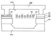
도3은 2축(dual-axis) 마이크로-스캐너 미러(309)의 예를 평면도로 나타내고 있다. 도3에서, 서스펜션들(312)을 가진 미러 플레이트(311) 및 주변 영역들이 도시되어 있다. 콤 전극들(comb electrodes)(도3에 도시 안됨)을 갖는 이 컴포넌트의 내측 영역은, 표면이 연마된, 토포그라피-프리(topography-free) 프레임(310)에 의 해 둘러싸여 있다. 이 프레임(310)은 그의 지형으로부터의 자유로움에 의해 밀봉 웨이퍼 레벨 패키지에 대한 접합면을 형성한다. 영역(308)은 액튜에이터 캡슐 외측의 영역을 나타낸다.FIG. 3 is a plan view of an example of a dual-
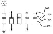
콤형 전극들의 여러 가지 설계들 및 활성화들을 도4 내지 도6에서 간단하게 설명한다. 상기 콤 전극들의 높이 오프셋을 얻도록, 가동 구조물, 즉 액튜에이터 소자에, 하부 에피폴리 층(503)에 의해 단독으로 형성된, 콤 전극들이 갖추어져 있는 한편, 서로 절연된, 양 에피폴리 층들(503,507)로부터 정적 카운터 콤 전극들이 생성된다. 이 도면 및 다음의 두 개의 도면들에 전기 활성화가 나타내진다.Various designs and activations of the comb-like electrodes are briefly described in Figures 4-6. From both epitaxial poly layers 503 and 507 insulated from one another while comb electrodes are provided on the movable structure, i.e., the actuator element, by the
이와 다르게, 도5에 도시된 바와 같이, 상기 가동 구조물에는 또한, 양 에피폴리 층들(603,607)로 구조화된, 콤 전극들이 갖추어질 수 있는 한편, 상기 목적을 위한 정적 카운터 콤 전극이 하부 에피폴리 층(603)에 의해서만 형성되어 있다.Alternatively, as shown in Figure 5, the movable structure may also be equipped with comb electrodes, structured with both epi poly layers 603 and 607, while a static counter comb electrode for this purpose is provided on the lower epi poly layer (603).
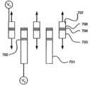
다른 대안으로서, 바람직하게 정적 콤 구조인, 콤 구조들 중 하나가 적어도 하부 층들, 즉 기판(701) 및 에피폴리 층(703)으로 형성되는 한편, 상기 가동 카운터 콤 구조물은 바람직하게 에피폴리 층들(703,707)로 구조화된다. 에피폴리 층(707)으로 형성된 콤 구조 컴포넌트들이 포텐셜 V1로 설정된 경우, 에피폴리 층(703)으로 형성된 컴포넌트들은, 그러운드 등의, 그와 다른 포텐셜로 일관되게 설정되며, 기판(701)으로 제조된 컴포넌트들이 포텐셜 V2로 설정된 경우, 두 개의 높이-오프셋 콤 구동부들의 형태는 서로 적층된 결과들로 되어, 단일 높이-오프셋 콤 구동부보다 큰 힘을 발휘할 수 있다. 이 타입의 구조화의 다른 장점은, 대향하는 전극들의 커패시턴스가 수직으로 상대적인 이동 중에 간격을 두고 크게 적어도 두 번 변화하므로, 서스펜드형 가동 콤 구조물이 수직 스트로크를 크게 적어도 두 번 실행할 수 있다는 점이다. 이는 에피폴리 층들(703,707)이 동일 두께를 가지는 것으로 가정한 것이다.As another alternative, one of the comb structures, which is preferably a static comb structure, is formed of at least the bottom layers, i.e., the
마지막으로, 도7은 제조된 마이크로-스캐너 미러가 커버 플레이트 및 바닥 플레이트의 부착에 의해 웨이퍼 레벨 상에 밀폐되어 밀봉된 캡슐화된 상태의 예를 나타내고 있다. 3개의 웨이퍼들을 포함하는 전체 웨이퍼 레벨 패키지가 이 경우에 단면도로 도시되어 있다. 사전처리된 글라스 커버 웨이퍼(108)가, 그 위에 배치된 층들을 가진, 기판(101), MEMS 웨이퍼의 상부 측에 양극 접합된다. 이는, 상부 측에 에피폴리 층(107)이 형성되고, 표면이 추가로 연마된, 상기 내측 영역 주위에서 중단되지 않고 주변 프레임에 의해 가능하게 된다. 상기 글라스 커버 웨이퍼(108)는, 캡슐화된 영역 내측에서의 액튜에이터 소자의 의도된 이동을 허용하는, 적절한 공동들(109)을 가진다. 또한, 상기 MEMS 웨이퍼는, 양극 또는 공융에 의해 접합되는, 글라스 바닥 웨이퍼(110)에 의해 후면에서 폐쇄된다. 이는 웨이퍼 기판(101)의 후면의 높은 표면 재질 때문에 문제를 일으키지 않게 된다.Finally, FIG. 7 shows an example of an encapsulated state in which the manufactured micro-scanner mirror is hermetically sealed on a wafer level by attachment of a cover plate and a bottom plate. An entire wafer-level package comprising three wafers is shown in cross-section in this case. A pretreated
예시적인 실시예들에 도시된 바와 같이, 상기 제안된 방법은, 예컨대, 정전기적으로 구동되는 단축 및 다축 마이크로-스캐너 미러들의 제조에 적합하다. 상기 방법은, 수직의 높이-오프셋을 가지며 서로 분리된 포텐셜들을 통해 활성화될 수 있는, 핑거형 또는 콤형 구동 전극들의 제조를 허용한다. 이 두 개의 레벨들 사이의 부가적인 와이어링 레벨이 서로 절연된 센서 포텐셜들 또는 임의의 수의 활성화가 실행되도록 허용한다. 상기 컴포넌트의 내측 영역을 둘러싸며 적어도 최상부 반 도체층에 의해 형성된 폐쇄된 프레임이, 예컨대, 양극 또는 공융에 의한 웨이퍼 접합에 의해 밀폐되어 밀봉된 웨이퍼 레벨 패키지의 형성을 허용한다. 집적되어 매립된 도체 레벨이 외부 단자 영역들을 측면 통과구들에 의해, 밀폐되어 밀봉된 캡슐에 대해 필요한 프레임의 표면 재질을 손상시키지 않고, 액튜에이터의 전극들에 접속한다. 미러 플레이트, 서스펜션 구조물들, 및 전극들은 상기 방법 시퀀스에 의해 적어도 3개의 다른 층 두께로 서로 독립적으로 실시될 수 있다. 동적 미러 변형의 문제는 다른 굽힘 강성들을 갖는 국부적으로 선택 가능한 이들 3개의 층들에 의해 바람직하게 상쇄될 수 있다.As shown in the exemplary embodiments, the proposed method is suitable, for example, for the fabrication of electrostatically driven single-axis and multi-axis micro-scanner mirrors. The method allows the fabrication of finger-like or comb-shaped driving electrodes, which can be activated through discrete potentials with vertical height-offsets. The additional wiring level between these two levels allows for mutually insulated sensor potentials or any number of activations to be performed. A closed frame formed by at least the uppermost semi-conductor layer surrounding the inner region of the component permits the formation of a sealed wafer-level package, for example, by wafer bonding by anodic or eutectic. The integrated buried conductor level connects the external terminal regions to the electrodes of the actuator by the side passage apertures without damaging the surface material of the frame necessary for the sealed encapsulated capsule. The mirror plates, the suspension structures, and the electrodes may be implemented independently of each other in at least three different layer thicknesses by the method sequence. The problem of dynamic mirror deformation can be offset preferably by these three locally selectable layers with different flexural stiffnesses.
Claims (11)
Translated fromKoreanApplications Claiming Priority (3)
| Application Number | Priority Date | Filing Date | Title |
|---|---|---|---|
| DE102006058563.1 | 2006-12-12 | ||
| DE102006058563ADE102006058563B3 (en) | 2006-12-12 | 2006-12-12 | Micromirror actuator with encapsulation option and method of manufacture |
| PCT/DE2007/002226WO2008071172A1 (en) | 2006-12-12 | 2007-12-11 | Micromirror actuator with encapsulation possibility and method for production thereof |
Publications (2)
| Publication Number | Publication Date |
|---|---|
| KR20090098801A KR20090098801A (en) | 2009-09-17 |
| KR101437193B1true KR101437193B1 (en) | 2014-09-03 |
Family
ID=39246820
Family Applications (1)
| Application Number | Title | Priority Date | Filing Date |
|---|---|---|---|
| KR1020097011120AActiveKR101437193B1 (en) | 2006-12-12 | 2007-12-11 | Micromirror actuator having encapsulation possibility and manufacturing method thereof |
Country Status (7)
| Country | Link |
|---|---|
| US (1) | US8169678B2 (en) |
| EP (1) | EP2100179B1 (en) |
| JP (1) | JP5486312B2 (en) |
| KR (1) | KR101437193B1 (en) |
| CA (1) | CA2672797C (en) |
| DE (1) | DE102006058563B3 (en) |
| WO (1) | WO2008071172A1 (en) |
Families Citing this family (22)
| Publication number | Priority date | Publication date | Assignee | Title |
|---|---|---|---|---|
| DE102008041178B4 (en) | 2008-08-12 | 2018-11-15 | Robert Bosch Gmbh | Manufacturing method for a micromechanical component |
| DE102008042967B4 (en) | 2008-10-20 | 2017-04-06 | Robert Bosch Gmbh | Cascaded micromechanical actuator structure |
| DE102010000878B4 (en)* | 2010-01-14 | 2022-04-28 | Robert Bosch Gmbh | Micromechanical component, optical device, manufacturing method for a micromechanical component and manufacturing method for an optical device |
| DE102011081002B4 (en) | 2011-08-16 | 2020-01-16 | Robert Bosch Gmbh | Manufacturing process for a micromechanical component |
| US9466532B2 (en) | 2012-01-31 | 2016-10-11 | Taiwan Semiconductor Manufacturing Company, Ltd. | Micro-electro mechanical system (MEMS) structures with through substrate vias and methods of forming the same |
| JP6046443B2 (en)* | 2012-10-19 | 2016-12-14 | 国立大学法人東北大学 | Manufacturing method of micromirror device |
| EP3056467B1 (en) | 2013-02-20 | 2017-05-24 | Harman Becker Automotive Systems GmbH | Circuit board comprising spatial light modulator |
| US9201239B1 (en)* | 2014-03-07 | 2015-12-01 | Advanced Numicro Systems, Inc. | Two-dimensional electrostatic scanner with distributed springs |
| DE102016107461A1 (en)* | 2016-04-22 | 2017-10-26 | Eto Magnetic Gmbh | Actuator device and method for operating an actuator device |
| EP3538945A1 (en) | 2016-11-09 | 2019-09-18 | Fraunhofer Gesellschaft zur Förderung der Angewand | Image generation device |
| DE102016221933A1 (en) | 2016-11-09 | 2018-05-09 | Fraunhofer-Gesellschaft zur Förderung der angewandten Forschung e.V. | Imaging device |
| US10112822B2 (en)* | 2017-02-16 | 2018-10-30 | Taiwan Semiconductor Manufacturing Co., Ltd. | Semiconductor device |
| DE102017208855A1 (en)* | 2017-05-24 | 2018-11-29 | Robert Bosch Gmbh | Micromirror device with mechanical stop |
| DE102017111642A1 (en)* | 2017-05-29 | 2017-08-10 | Eto Magnetic Gmbh | Small appliances device |
| EP3650909B1 (en) | 2017-07-06 | 2023-11-15 | Hamamatsu Photonics K.K. | Optical module |
| JP7090249B2 (en)* | 2019-06-06 | 2022-06-24 | 国立大学法人 東京大学 | Manufacturing method for manufacturing electrostatic devices |
| JP2020202613A (en)* | 2019-06-06 | 2020-12-17 | 国立大学法人 東京大学 | Electrostatic device and manufacturing method thereof |
| DE102020114347B3 (en)* | 2020-05-28 | 2021-10-28 | Infineon Technologies Ag | MEMS devices with spring element and comb drive and related manufacturing processes |
| CN114594594B (en)* | 2022-05-11 | 2022-08-02 | 西安知象光电科技有限公司 | Electrostatic driving MEMS comb tooth structure, micro mirror adopting structure and preparation method of micro mirror |
| DE102023107984A1 (en)* | 2023-03-29 | 2024-10-02 | OQmented GmbH | LAYER STRUCTURE FOR A MEMS DEVICE, METHOD FOR PRODUCING THE LAYER STRUCTURE AND MEMS DEVICE |
| WO2024262188A1 (en)* | 2023-06-20 | 2024-12-26 | 富士フイルム株式会社 | Micromirror device and optical scanning apparatus |
| DE102023209645A1 (en) | 2023-09-29 | 2025-04-03 | Robert Bosch Gesellschaft mit beschränkter Haftung | Microelectromechanical transducer element and microelectromechanical component with a transducer element |
Citations (3)
| Publication number | Priority date | Publication date | Assignee | Title |
|---|---|---|---|---|
| JP2004145032A (en)* | 2002-10-24 | 2004-05-20 | Fujitsu Ltd | Manufacturing method of microstructure |
| US20050213230A1 (en)* | 2004-03-10 | 2005-09-29 | Eiji Mochizuki | Optical scanning device and method of manufacturing the same |
| JP2006156815A (en)* | 2004-11-30 | 2006-06-15 | Matsushita Electric Works Ltd | Airtight device and its manufacturing method |
Family Cites Families (11)
| Publication number | Priority date | Publication date | Assignee | Title |
|---|---|---|---|---|
| JPH06310615A (en)* | 1993-04-21 | 1994-11-04 | Seiko Epson Corp | Semiconductor enclosure formation and piezoelectric oscillator loaded on semiconductor substrate |
| WO1996039643A1 (en)* | 1995-06-05 | 1996-12-12 | Nihon Shingo Kabushiki Kaisha | Electromagnetic actuator |
| WO1997002506A1 (en)* | 1995-06-30 | 1997-01-23 | Cms Mikrosysteme Gmbh Chemnitz | Pivoting micro-actuators and method for their production |
| US6146917A (en)* | 1997-03-03 | 2000-11-14 | Ford Motor Company | Fabrication method for encapsulated micromachined structures |
| US7079299B1 (en)* | 2000-05-31 | 2006-07-18 | The Regents Of The University Of California | Staggered torsional electrostatic combdrive and method of forming same |
| US7307775B2 (en)* | 2000-12-07 | 2007-12-11 | Texas Instruments Incorporated | Methods for depositing, releasing and packaging micro-electromechanical devices on wafer substrates |
| US20090065429A9 (en)* | 2001-10-22 | 2009-03-12 | Dickensheets David L | Stiffened surface micromachined structures and process for fabricating the same |
| DE60223136D1 (en)* | 2002-06-20 | 2007-12-06 | St Microelectronics Srl | Microelectromechanical component, in particular microactuator for hard disk units, and method for its production |
| US7045868B2 (en)* | 2003-07-31 | 2006-05-16 | Motorola, Inc. | Wafer-level sealed microdevice having trench isolation and methods for making the same |
| US7329930B2 (en)* | 2004-03-08 | 2008-02-12 | Opus Microsystems Corporation | Micromechanical actuator with multiple-plane comb electrodes and methods of making |
| JP4390194B2 (en)* | 2004-03-19 | 2009-12-24 | 株式会社リコー | Deflection mirror, deflection mirror manufacturing method, optical writing apparatus, and image forming apparatus |
- 2006
- 2006-12-12DEDE102006058563Apatent/DE102006058563B3/enactiveActive
- 2007
- 2007-12-11JPJP2009540596Apatent/JP5486312B2/enactiveActive
- 2007-12-11KRKR1020097011120Apatent/KR101437193B1/enactiveActive
- 2007-12-11CACA2672797Apatent/CA2672797C/enactiveActive
- 2007-12-11EPEP07856077.8Apatent/EP2100179B1/enactiveActive
- 2007-12-11USUS12/517,241patent/US8169678B2/enactiveActive
- 2007-12-11WOPCT/DE2007/002226patent/WO2008071172A1/enactiveApplication Filing
Patent Citations (3)
| Publication number | Priority date | Publication date | Assignee | Title |
|---|---|---|---|---|
| JP2004145032A (en)* | 2002-10-24 | 2004-05-20 | Fujitsu Ltd | Manufacturing method of microstructure |
| US20050213230A1 (en)* | 2004-03-10 | 2005-09-29 | Eiji Mochizuki | Optical scanning device and method of manufacturing the same |
| JP2006156815A (en)* | 2004-11-30 | 2006-06-15 | Matsushita Electric Works Ltd | Airtight device and its manufacturing method |
Also Published As
| Publication number | Publication date |
|---|---|
| JP2010512548A (en) | 2010-04-22 |
| US8169678B2 (en) | 2012-05-01 |
| KR20090098801A (en) | 2009-09-17 |
| JP5486312B2 (en) | 2014-05-07 |
| CA2672797A1 (en) | 2008-06-19 |
| EP2100179A1 (en) | 2009-09-16 |
| EP2100179B1 (en) | 2013-11-06 |
| CA2672797C (en) | 2015-03-31 |
| WO2008071172A1 (en) | 2008-06-19 |
| US20100085622A1 (en) | 2010-04-08 |
| DE102006058563B3 (en) | 2008-06-19 |
Similar Documents
| Publication | Publication Date | Title |
|---|---|---|
| KR101437193B1 (en) | Micromirror actuator having encapsulation possibility and manufacturing method thereof | |
| KR101659638B1 (en) | Layered mems structure and method thereof | |
| US7104129B2 (en) | Vertically integrated MEMS structure with electronics in a hermetically sealed cavity | |
| US7247246B2 (en) | Vertical integration of a MEMS structure with electronics in a hermetically sealed cavity | |
| US5834332A (en) | Micromechanical semiconductor components and manufacturing method therefor | |
| US9411154B2 (en) | Micro-electromechanical reflector and method for manufacturing a micro-electromechanical reflector | |
| KR20040035116A (en) | 2-dimensional actuator and manufacturing method thereof | |
| JP2012042228A (en) | Micro-electromechanical system and manufacturing method thereof | |
| JP2009226499A (en) | Micromechanical apparatus and manufacturing method of micromechanical apparatus | |
| US8630033B2 (en) | Via structure and method thereof | |
| US20020126455A1 (en) | Tiled microelectromechanical device modules and fabrication methods | |
| US11267697B2 (en) | Use of an uncoupling structure for assembling a component having a casing | |
| US7531424B1 (en) | Vacuum wafer-level packaging for SOI-MEMS devices | |
| US8729713B2 (en) | Via structure and method thereof | |
| JP2009226497A (en) | Micromechanical apparatus and manufacturing method of micromechanical apparatus | |
| JP2009226498A (en) | Micromechanical apparatus and manufacturing method of micromechanical apparatus | |
| JP2009178816A (en) | Micromachine device and method of manufacturing micromachine device | |
| HK1161362A (en) | Mems device | |
| HK1161363A (en) | Semiconductor device comprising a cavity having a vent hole | |
| HK1161363B (en) | Semiconductor device comprising a cavity having a vent hole |
Legal Events
| Date | Code | Title | Description |
|---|---|---|---|
| PA0105 | International application | St.27 status event code:A-0-1-A10-A15-nap-PA0105 | |
| PG1501 | Laying open of application | St.27 status event code:A-1-1-Q10-Q12-nap-PG1501 | |
| A201 | Request for examination | ||
| P11-X000 | Amendment of application requested | St.27 status event code:A-2-2-P10-P11-nap-X000 | |
| P13-X000 | Application amended | St.27 status event code:A-2-2-P10-P13-nap-X000 | |
| PA0201 | Request for examination | St.27 status event code:A-1-2-D10-D11-exm-PA0201 | |
| E902 | Notification of reason for refusal | ||
| PE0902 | Notice of grounds for rejection | St.27 status event code:A-1-2-D10-D21-exm-PE0902 | |
| P11-X000 | Amendment of application requested | St.27 status event code:A-2-2-P10-P11-nap-X000 | |
| P13-X000 | Application amended | St.27 status event code:A-2-2-P10-P13-nap-X000 | |
| E701 | Decision to grant or registration of patent right | ||
| PE0701 | Decision of registration | St.27 status event code:A-1-2-D10-D22-exm-PE0701 | |
| GRNT | Written decision to grant | ||
| PR0701 | Registration of establishment | St.27 status event code:A-2-4-F10-F11-exm-PR0701 | |
| PR1002 | Payment of registration fee | St.27 status event code:A-2-2-U10-U12-oth-PR1002 Fee payment year number:1 | |
| PG1601 | Publication of registration | St.27 status event code:A-4-4-Q10-Q13-nap-PG1601 | |
| PR1001 | Payment of annual fee | St.27 status event code:A-4-4-U10-U11-oth-PR1001 Fee payment year number:4 | |
| FPAY | Annual fee payment | Payment date:20180821 Year of fee payment:5 | |
| PR1001 | Payment of annual fee | St.27 status event code:A-4-4-U10-U11-oth-PR1001 Fee payment year number:5 | |
| R18-X000 | Changes to party contact information recorded | St.27 status event code:A-5-5-R10-R18-oth-X000 | |
| FPAY | Annual fee payment | Payment date:20190816 Year of fee payment:6 | |
| PR1001 | Payment of annual fee | St.27 status event code:A-4-4-U10-U11-oth-PR1001 Fee payment year number:6 | |
| PR1001 | Payment of annual fee | St.27 status event code:A-4-4-U10-U11-oth-PR1001 Fee payment year number:7 | |
| PR1001 | Payment of annual fee | St.27 status event code:A-4-4-U10-U11-oth-PR1001 Fee payment year number:8 | |
| PR1001 | Payment of annual fee | St.27 status event code:A-4-4-U10-U11-oth-PR1001 Fee payment year number:9 | |
| PR1001 | Payment of annual fee | St.27 status event code:A-4-4-U10-U11-oth-PR1001 Fee payment year number:10 | |
| PR1001 | Payment of annual fee | St.27 status event code:A-4-4-U10-U11-oth-PR1001 Fee payment year number:11 | |
| PR1001 | Payment of annual fee | St.27 status event code:A-4-4-U10-U11-oth-PR1001 Fee payment year number:12 |