KR101428066B1 - vertical structured group 3 nitride-based light emitting diode and its fabrication methods - Google Patents
vertical structured group 3 nitride-based light emitting diode and its fabrication methodsDownload PDFInfo
- Publication number
- KR101428066B1 KR101428066B1KR1020080030919AKR20080030919AKR101428066B1KR 101428066 B1KR101428066 B1KR 101428066B1KR 1020080030919 AKR1020080030919 AKR 1020080030919AKR 20080030919 AKR20080030919 AKR 20080030919AKR 101428066 B1KR101428066 B1KR 101428066B1
- Authority
- KR
- South Korea
- Prior art keywords
- layer
- ohmic contact
- contact electrode
- emitting diode
- type
- Prior art date
- Legal status (The legal status is an assumption and is not a legal conclusion. Google has not performed a legal analysis and makes no representation as to the accuracy of the status listed.)
- Expired - Fee Related
Links
Images


Landscapes
- Led Devices (AREA)
Abstract
Translated fromKoreanDescription
Translated fromKorean본 발명은 그룹 3족 질화물계 반도체로 구성된 발광구조체를 중심으로 n형 오믹접촉 전극구조체와 p형 오믹접촉 전극구조체가 상하로 대향 되게 위치하고, 상기 발광구조체와 기계 가공된 전기전도성인 히트씽크 지지대를 최소 300℃ 이상의 온도에서 결합시키는 전도성 웨이퍼 결합층을 이용하여 제조되는 차세대 수직구조 그룹 3족 질화물계 반도체 발광다이오드 소자 및 그의 제조 방법을 제공한다.The present invention is characterized in that an n-type ohmic contact electrode structure and a p-type ohmic contact electrode structure are vertically opposed to each other around a light emitting structure composed of group III nitride-based semiconductors, and the light emitting structure and the machined electrically conductive heat sink support The present invention provides a next generation vertical structure group III nitride-based semiconductor light emitting diode device and a method of manufacturing the same, which are manufactured using a conductive wafer bonding layer bonding at a temperature of at least 300 캜.
발광다이오드(light emitting diode; LED) 및 레이저다이오드(laser diode; LD) 등의 발광소자는 p-n결합에 순방향으로 전류를 흐르게 함으로써 빛을 발생시키는 고체 반도체 장치이다. 특히 고체 반도체를 이용한 발광다이오드 소자는 전기에너지를 빛에너지로 변환하는 효율이 높고 수명이 5~10년 이상으로 길며 전력 소모와 유지 보수비용을 크게 절감할 수 있는 장점이 있어서 차세대 디스플레이 및 조명용 기기 응용 분야에서 주목받고 있다.BACKGROUND ART Light emitting devices such as light emitting diodes (LEDs) and laser diodes (LDs) are solid state semiconductor devices that generate light by flowing a current in a forward direction to a p-n junction. In particular, LED devices using solid-state semiconductors have a high efficiency of converting electrical energy into light energy, have a long life span of 5 to 10 years, and can save power and maintenance costs. Has attracted attention in the field.
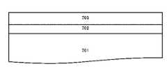
일반적으로 그룹 3족 질화물계 반도체 발광다이오드 소자는 투명한 사파이 어(sapphire) 성장기판 상면에 성장하지만, 사파이어 성장기판은 단단하고 전기적으로 절연성이며 열전도 특성이 뛰어나지 않아 그룹 3족 질화물계 반도체 발광다이오드 소자의 크기를 줄여 제조원가를 절감하거나, 광추출 효율, 또는 정전기 방전(electrostatic discharge; 이하, 'ESD'라 칭함) 같은 단위칩의 특성을 개선시키는데 한계가 있다. 다시 말하자면, 사파이어 성장기판은 전기적으로 절연체이므로, 그룹 3족 질화물계 반도체 발광다이오드 소자의 구조에 있어서 큰 제약을 미친다. 도 1에 도시된 바와 같이, 사파이어 성장기판 상면에 형성된 종래의 그룹 3족 질화물계 반도체 발광다이오드 소자의 구조를 통해 구체적으로 설명하기로 한다.In general, a group III nitride-based semiconductor light-emitting diode device is grown on the surface of a transparent sapphire growth substrate. However, since the sapphire growth substrate is hard, electrically insulating, and not excellent in heat conduction characteristics, a group III nitride semiconductor light- There is a limit in improving the characteristics of the unit chip such as reducing the manufacturing cost by reducing the size, light extraction efficiency, or electrostatic discharge (ESD). In other words, since the sapphire growth substrate is electrically insulative, it poses a great limitation in the structure of the group III nitride-based semiconductor light-emitting diode device. As shown in FIG. 1, the structure of a conventional Group III nitride-based semiconductor light emitting diode device formed on the upper surface of a sapphire growth substrate will be described in detail.
도 1은 종래의 그룹 3족 질화물계 반도체 발광다이오드 소자의 단면도이다. 그룹 3족 질화물계 반도체 발광다이오드 소자용 발광구조체는 사파이어 성장기판(10) 상면에 성장되는데, 이러한 종래의 그룹 3족 질화물계 반도체 발광다이오드 소자는 성장기판(10)과 그 성장기판(10) 상에 형성된 그룹 3족 질화물계 반도체 발광다이오드 소자용 발광구조체(20, 30, 40)를 포함한다.1 is a cross-sectional view of a conventional Group III nitride-based semiconductor light-emitting diode device. The light emitting structure for the group III nitride-based semiconductor light-emitting diode device is grown on the upper surface of the
상기 그룹 3족 질화물계 반도체 발광다이오드 소자용 발광구조체(20, 30, 40)는 상기 성장기판(10) 상에 순차적으로 형성된 n형 질화물계 클래드층(20)과 다중양자우물(Multi-Quantum Well)구조의 질화물계 활성층(30)과 p형 질화물계 클래드층(40)으로 구성된다. 상기 발광다이오드 소자용 발광구조체는 MOCVD 등의 공정을 이용하여 성장될 수 있다. 이 때, n형 질화물계 클래드층(20)을 성장하기 전에 성장기판(10)과의 격자정합 및 열팽창 계수 차이로 발생하는 응력을 완화하기 위해서, AlN 또는 GaN으로 이루어진 완충층(미도시)을 형성할 수도 있다.The
또한, 소정의 영역에 해당하는 p형 질화물계 클래드층(40)과 질화물계 활성층(30)을 건식 식각하여 n형 질화물계 클래드층(20) 일부 상면을 대기에 노출시키고, 그 노출된 n형 질화물계 클래드층(20) 상면과 p형 질화물계 클래드층(40) 상면에 각각 소정의 전압을 인가하기 위한 p형 오믹접촉 전극 및 패드(60)와 n형 오믹접촉 전극 및 패드(70)를 형성한다. 일반적으로 전류주입 면적을 증가시키면서도 휘도에 악영향을 주지 않기 위해서, p형 질화물계 클래드층(40) 및 n형 질화물계 클래드층(20) 상면에는 상기 p형 오믹접촉 전극 및 패드(60)와 n형 오믹접촉 전극 및 패드(70)를 형성하기 전에 투명성 커런트 스프레딩층(transparent current spreading layer)를 형성할 수도 있다. 도 1에서는 p형 질화물계 클래드층(40)과 p형 전극 및 패드(60) 사이에 위치하는 투명성 커런트 스프레딩층(50)를 도시하고 있다.The p-type nitride-based
이와 같이, 기존의 그룹 3족 질화물계 반도체 발광다이오드 소자는 전기절연체인 사파이어 성장기판(10)을 사용하기 때문에, 두 오믹접촉 전극 및 패드(60, 70)를 수평한 방향으로 나란하게 형성시킬 수밖에 없다. 따라서 외부전압 인가 시에 n형 오믹접촉 전극 및 패드(70)로부터 질화물계 활성층(30)을 통해 p형 오믹접촉 전극 및 패드(60)로 향하는 전류 흐름이 수평방향을 따라 협소하게 형성될 수밖에 없다. 이러한 협소한 전류 흐름으로 인해서 상기 그룹 3족 질화물계 반도체 발광다이오드 소자는 순방향 전압(forward voltage)이 증가하여 전류 주입효율을 격감시키고 (“커런트 크라우딩 현상” 말함), 이로 인해서 정전기 방전(electrostatic discharge)효과가 취약하다는 문제가 발생한다.As described above, since the conventional Group III nitride-based semiconductor light-emitting diode device uses the
또한, 종래의 그룹 3족 질화물계 반도체 발광다이오드 소자에서는, 전류밀도의 증가에 의해 대량의 열이 발생하게 되고, 반면에 사파이어 성장기판(10)의 낮은 열전도도에 의해 외부로의 열방출이 원할 하지 못하므로, 전류밀도 증가에 따라 사파이어 성장기판(10)과 발광다이오드 소자용 발광구조체 간에 기계적 응력이 발생되어 소자의 전기 및 광학적 특성에 영향을 미치게 된다.In addition, in the conventional group III nitride-based semiconductor light-emitting diode device, a large amount of heat is generated due to an increase in the current density. On the other hand, heat dissipation to the outside due to low thermal conductivity of the
더 나아가서는 종래의 그룹 3족 질화물계 반도체 발광다이오드 소자에서는, n형 오믹접촉 전극 및 패드(70)를 형성하기 위해, 적어도 형성할 n형 오믹접촉 전극 및 패드(70)의 면적보다 크게 질화물계 활성층(30)의 일부 영역을 제거하여야 하므로, 발광면적이 감소하여 소자크기 대 휘도에 따른 발광효율이 저하된다는 문제도 있다.Furthermore, in order to form the n-type ohmic contact electrode and the
상기한 전기절연성인 사파이어 성장기판(10) 상면에 형성된 그룹 3족 질화물계 반도체 발광다이오드 소자의 문제점을 극복하고, 높은 에너지 전환효율을 갖는 동시에 고휘도 발광 특성을 갖는 그룹 3족 질화물계 반도체 발광다이오드 소자를 구현하기 위해서는 발광소자 구동 시에 외부에서 대용량 전기에너지를 인가하거나 대면적의 단위칩을 제조해야 한다. 현재 높은 에너지 전환효율을 갖는 동시에 고휘도 발광 특성을 갖는 발광다이오드 소자 구현은 비교적 용이한 방식인 발광다이오드 소자에 대전류(즉, 대용량)를 인가하여 수행하고 있지만, 대전류 인가 시에 필연적으로 발생하는 다량의 열방출 문제를 해결하는데 어려움을 겪고 있는 실정이다.Based group III nitride semiconductor light emitting diode device having a high energy conversion efficiency and a high luminance emission characteristic, which overcomes the problems of the group III nitride based semiconductor light emitting diode device formed on the upper surface of the
최근 새로운 대안으로서, 독일의 오스람(OSRAM) 사가 성장기판 제거를 통한 박막 질화갈륨 발광다이오드(thinGaN LED)라는 수직구조 그룹 3족 질화물계 반도체 발광다이오드 소자 제품을 레이저 리프트 오프(laser lift-off) 성장기판 제거 기술을 접목하여 개발하였고, 그 이외의 몇몇 선진 회사들도 유사한 형태의 수직구조 그룹 3족 질화물계 반도체 발광다이오드 소자 개발에 주력하고 있다.Recently, as a new alternative, OSRAM, Germany, has developed a vertical structure group III nitride-based semiconductor light-emitting diode device called thin-GaN LED through growth substrate removal as a laser lift-off growth Substrate removal technology has been developed and developed, and some advanced companies are also focusing on the development of similar type vertical structure Group III nitride-based semiconductor light-emitting diode devices.
상기 투명한 성장기판 제거를 통한 높은 에너지 전환효율을 갖는 동시에 고휘도 발광 특성을 갖는 수직구조 그룹 3족 질화물계 반도체 발광다이오드 소자 제조는 사파이어 성장기판(10)의 제거만 확실하게 수행된다면 제조 공정 및 단가를 월등히 혁신시킬 수 있다. 이외에도, 사파이어 성장기판(10) 상면에 형성된 그룹 3족 질화물계 반도체 발광다이오드 소자 제조의 경우 발광면적이 단위칩 면적의 약 50% 정도인데 비하여, 사파이어 성장기판(10)이 제거된 수직구조 발광다이오드 소자의 경우 발광면적이 단위칩 면적의 90% 정도에 이르므로 경제적 및 기술적 관점에서도 사파이어 성장기판(10)을 포함한 수평구조의 발광다이오드 소자에 비해 훨씬 유리하다. 그러나 여전히 상기 사파이어 성장기판(10)을 포함한 수평구조의 발광다이오드 소자와 사파이어 성장기판(10) 제거 방식을 이용한 수직구조 발광다이오드 소자는 일정한 단위칩 발광면적을 갖는 소자에 대전류를 인가하는 방식이라 에너지 전환효율(‘외부에서 인가한 전기에너지 대 방출한 광에너지’ 정의)이 뛰어나지가 않다.If the
따라서 차세대 높은 에너지 전환효율 및 고휘도 특성을 갖는 그룹 3족 질화물계 발광다이오드 소자를 구현하기 위해서는 가능한 대면적 저전류 주입 방식을 이용하는 것이 기술 및 경제적인 면에서 훨씬 유리하다.Therefore, in order to realize a group III nitride-based light emitting diode device having the next generation high energy conversion efficiency and high luminance characteristic, it is more advantageous from the technical and economical point of view to use a large-area low current injection method as much as possible.
현재 상기 사파이어 성장기판(10)을 포함한 수평구조의 발광다이오드 소자는 낮은 p형 질화물계 클래드층의 전기전도성으로 인한 전류밀집(current crowding) 현상이 발생하여 대면적 발광다이오드 소자 제조에 원천적으로 기술적 제한이 있다. 또한 상기 사파이어 성장기판(10) 제거 방식을 이용한 수직구조 발광다이오드 소자도 발광소자 제조 시에 이용되는 레이저빔(laser beam) 크기 제한으로 인하여 대면적 수직구조 발광소자를 제조하여 저전력 주입을 통한 고휘도 특성을 갖는 광원을 확보하기엔 쉽지 않다. 일반적으로 기존의 레이저 리프트 오프 방식은 1스퀘어센티미터(one square centimeters) 면적을 갖는 균일하고 강한 에너지원의 레이저빔을 조사할 수 있기 때문에, 상기 레이저빔을 조사하기 전에 고체 반도체 박막의 손상 및 크랙(crack) 전파를 최소화하기 위해서 건식 에칭(dry etching) 공정으로 사파이어 성장기판(10)까지 트렌치(trench)를 이용하여 섬화 공정(isolation processing)을 수행해야 한다. 상기 섬화 공정은 그룹 3족 질화물계 반도체 박막 내 미세 크랙 발생과 주위(generation and propagation of crack)로의 전파를 방지하기 위한 기술이다. 그러나 상기 레이저 리프트 오프 방식에 의해 전기전도성 지지대에 전이(transfer)시킨 소정의 발광면적으로 섬화(isolation)된 발광다이오드 소자용 발광구조체 면적은 사용된 레이저빔 모양 및 크기에 제한적이므로 수직구조 발광다이오드 소자의 크기를 자유롭게 증가시킬 수 없다.At present, the horizontal light emitting diode device including the
상기 트렌치를 통한 섬화 공정 이외에도, 차세대 광원으로서 그룹 3족 질화물계 반도체를 구성된 수직구조 발광다이오드 소자를 구현화하기 위해서는 무엇보다도 레이저 리프트 오프 방식 도입 시에 발생하는 반도체 박막층 손상을 최소화해 야 하는데, 이를 위해서는 성장기판(10)과 그룹 3족 질화물계 반도체 박막층 간에 존재하는 잠재 스트레스(latent stress)로 인한 크랙 발생 및 전파, 그리고 깨짐(breaking) 방지 목적으로, 발광다이오드 소자용 발광구조체 상면면에 밀착성이 뛰어난 지지대(support)를 형성하는 것이다. 상기 지지대는 레이저 리프트 오프 공정 시에 잠재 스트레스를 완화하는 역할 이외에, 동시에 열적 및 전기적으로 우수한 전도성이 있어 최종적으로 제조된 수직구조 발광다이오드 소자 구동 시에 발생하는 다량의 열을 외부로 방출시켜 주는 히트씽크(heat-sink) 역할과 전류주입을 하는 전극 및 패드로서 역할을 할 수 있어야 한다.In order to realize a vertically structured light emitting diode device constituted of group III nitride-based semiconductors as a next-generation light source in addition to the above-described trimming process through a trench, the damage of the semiconductor thin film layer occurring at the time of introducing the laser lift off method should be minimized. The upper surface of the light-emitting structure for the light-emitting diode device has excellent adhesion to the
현재 상기한 바와 같이, 레이저 리프트 오프 방식을 통한 수직구조 발광다이오드 소자 제조를 위한 지지대 형성 방법으로는 전기도금(electroplating)과 웨이퍼 결합(wafer bonding)이 주로 이용되고 있다.As described above, electroplating and wafer bonding are mainly used as a method of forming a support for manufacturing a vertical structure light emitting diode device through a laser lift-off method.
상기 전기도금에 의해 형성된 지지대를 이용하면 비교적 용이하게 수직구조 발광다이오드 소자를 제조할 수 있는 장점이 있지만, 최종적으로 제조된 수직구조 발광다이오드 소자의 전체적인 소자신뢰성에 심각한 문제점을 유발할 수 있는 많은 여지와 소자 성능 향상에 제한이 있다(도 2 참조). 반면에, 상기 웨이퍼 결합에 의해 형성된 지지대는 안정적인 소자신뢰성 확보와 소자 성능 향상에 잠재적인 여지가 많은 것이 장점이다. 이러한 웨이퍼 결합에 의해 지지대를 형성하는 공정은 열팽창계수(thermal expansion coefficient)가 다른 이종물질간의 웨이퍼 결합을 성공적으로 수행해야 한다. 하지만, 이종물질간의 웨이퍼 결합 후에 열적 스트레스로 인하여 성장기판 또는 반도체 박막층 내에 미세한 크랙 또는 깨짐 문제, 더 나 아가서는 비결합(debonding) 현상 등의 여러 심각한 문제점이 대두하고 있다(도 3 참조). 따라서, 현재 웨이퍼 결합을 통한 수직구조 발광다이오드 소자 제조는 300℃ 미만의 온도에서 웨이퍼 결합이 가능한 전도성 웨이퍼 결합층(일예, 유텍틱 공정 반응계)을 이용하고 있는 실정이다.The use of the supporting plate formed by the electroplating is advantageous in that a vertically structured light emitting diode device can be relatively easily manufactured. However, there is a lot of room for serious problems in the overall device reliability of the finally fabricated vertical light emitting diode device There is a limitation in device performance improvement (see FIG. 2). On the other hand, the support formed by the above-described wafer bonding is advantageous in securing stable device reliability and potentially increasing device performance. The process of forming the support by such wafer bonding must successfully perform wafer bonding between dissimilar materials having different thermal expansion coefficients. However, after bonding wafers between different materials, thermal stress causes various serious problems such as fine cracks or cracks in the growth substrate or semiconductor thin film layer, and further, debonding phenomenon (refer to FIG. 3). Thus, the fabrication of vertically-structured light-emitting diode devices through current wafer bonding utilizes a conductive wafer bonding layer (e. G., Eutectic process reaction system) capable of wafer bonding at temperatures below 300 ° C.
상기 전기도금(도 2 참조)과 웨이퍼 결합(도 3 참조)을 통해 전기전도성 지지대를 형성하고, 이를 통한 수직구조 발광다이오드 소자 제작에 대해서 더욱 더 상세하게 설명하자면, 하기와 같다.The fabrication of a vertically structured light emitting diode device through the electroplating (see FIG. 2) and the wafer bonding (see FIG. 3) through an electrically conductive support member will now be described in more detail.
상기 전기도금(electroplating)에 의해서 형성된 지지대(support)를 이용하여 수직구조 발광다이오드 소자 제조 공정은 도 2에 보인 바와 같다. 우선 성장기판(10) 상면에 기본적으로 n형 질화물계 클래드층(20), 질화물계 활성층(30), 및 p형 질화물계 클래드층(40)으로 구성된 발광다이오드 소자용 발광구조체를 성장 형성시키고 후(미도시)에 도 2A에 보인 바와 같이, 트렌치(80)를 이용하여 레이저빔 크기보다 작게 섬화 공정(isolation process)을 수행한다. 그런 후, 소자 패시베이션층(50)과 커런트 블라킹(current blocking) 영역을 포함한 반사층(60), 및 전기전도성 물질인 Ni, Cu 등의 금속 후막을 전기도금으로 형성시키기 위한 씨드층(70a)을 상기 발광다이오드 소자용 발광구조체의 상면 또는 측면에 형성시킨다. 그런 후에 도 2B에 보인 바와 같이, 상기 트렌치(80)된 영역에 유기물 포스트(90)를 세우고, 동시에 전기전도성 물질인 Ni, Cu 등의 금속 후막을 전기도금으로 형성시키기 위한 씨드층(70a)을 상기 유기물 포스트(90) 상면에도 형성시킨다. 그런 후에 도 2C에 보인 바와 같이, 상기 지지대(100) 역할을 하는 전기전도성 물질인 Ni, Cu 등의 금속 후막을 전기도금으로 형성시킨다. 그런 후에 도 2D에 보인 바와 같이, 상기 레이저 리프트 오프 방식을 이용하여 성장기판(10) 제거 및 레이저 리프트 오프 잔해물 등을 제거하는 평탄화 공정을 행한다. 그런 후에 도 2E에 보인 바와 같이, 대기 중으로 노출된 n형 질화물계 클래드층(20) 일부영역에 표면 거칠기(surface texture; 110)와 오믹접촉 전극 및 패드(120)를 형성한다. 그런 후에 도 2F에 보인 바와 같이, 마지막 공정으로서 기계 또는 레이저 가공을 통해서 단위칩을 완성한다.The process of fabricating a vertical structure light emitting diode device using a support formed by the electroplating is as shown in FIG. A light emitting structure for a light emitting diode element consisting essentially of an n-type nitride-based
상기 웨이퍼 결합(wafer bonding)에 의해서 형성된 지지대(support)를 이용하여 수직구조 발광다이오드 소자 제조 공정은 도 3에 보인 바와 같다. 우선 성장기판(10) 상면에 기본적으로 n형 질화물계 클래드층(20), 질화물계 활성층(30), 및 p형 질화물계 클래드층(40)으로 구성된 발광다이오드 소자용 발광구조체를 성장 형성시키고 후(미도시)에 도 3A에 보인 바와 같이, 트렌치(80)를 이용하여 레이저빔 크기보다 작게 섬화 공정(isolation process)을 수행한다. 그런 후, 소자 패시베이션층(50), 커런트 블라킹(current blocking) 영역을 포함한 반사층(60), 및 전도성 웨이퍼 결합층(70b)을 상기 발광다이오드 소자용 발광구조체의 상면 또는 측면에 형성시킨다. 그런 후에 도 3B에 보인 바와 같이, 상기 전도성 웨이퍼 결합층(70b)을 이용하여 전기전도성 기판인 Si 등을 지지대(140)로서 웨이퍼 결합한다. 그런 후에 도 3C에 보인 바와 같이, 상기 레이저 리프트 오프 방식을 이용하여 성장기판(10) 제거 및 레이저 리프트 오프 공정 잔해물 등을 제거하는 평탄화 공정을 행한다. 그런 후에 도 3D에 보인 바와 같이, 대기 중으로 노출된 n형 질화물계 클래 드층(20) 일부영역에 표면 거칠기(surface texture; 110)와 오믹접촉 전극 및 패드(120)를 형성한다. 그런 후에 도 3E에 보인 바와 같이, 마지막 공정으로서 기계 또는 레이저 가공을 통해서 단위칩을 완성한다.The process of fabricating the vertical structure light emitting diode device using a support formed by wafer bonding is as shown in FIG. A light emitting structure for a light emitting diode element consisting essentially of an n-type nitride-based
상술한 바와 같이, 종래 전기도금 및 웨이퍼 결합을 통한 지지대 형성 공정 기술을 이용한 수직구조 발광다이오드 소자 제조는 공통으로 성장기판(10)을 제거하기 전에 레이저빔 크기보다 작은 규격(scale)으로 발광다이오드 소자용 발광구조체를 단일화시키는 섬화 공정(isolation process)을 포함하고 있는 것이 특징이다. 이러한 섬화 공정을 이용한 수직구조 발광다이오드 소자 제조는 레이저빔 크기보다 더 큰 발광면적을 갖는 발광소자 제조를 어렵게 한다.As described above, the vertical structure light emitting diode device fabrication using conventional electroplating and wafer bonding process techniques is commonly used to manufacture a light emitting diode device with a scale smaller than the laser beam size before removing the
또한, 종래 전기도금 및 웨이퍼 결합을 통한 지지대 형성 공정 기술을 이용한 수직구조 발광다이오드 소자 제조는 공통으로 성장기판(10)을 제거시킨 후, 300℃ 이상의 온도에서 후공정(post-annealing)을 행할 수가 없어, 열적으로 안정한 고신뢰성 단일칩을 제조하기가 어렵다. 설령, 300℃ 이상의 열처리 공정을 거치지 않고 제조된 단일칩은 향후 조명용 광원으로서 이용하는데 많은 제한이 존재할 것으로 사료된다. 이러한 이유로, 전기도금에 의해서 형성된 지지대인 Ni, Cu 등의 전기도금 후막(thick film)은 치밀한 조직을 갖는 것이 아니라, 많은 기공(porosity)을 갖고 있는 비정질(amorphous) 또는 다결정(polycrystal)로 구성되어 있는 동시에, 후막 내에 다량의 황(S) 및 인(P) 성분이 첨가되어 있어 사용 시간과 더불어서 이들 물질들의 확산이 있게 되고, 결국엔 소자신뢰성에 문제를 야기하게 된다. 또한, 상기 웨이퍼 결합에 의해서 형성된 지지대는 열팽창계수 차이로 발생되는 응력을 최소화하기 위해서 300℃ 미만에 온도에서 결합이 형성되기 때문에, 300℃ 이상의 후공정을 행할 수가 없다.In addition, in the conventional vertical-type light-emitting diode device fabrication using the process of forming a support through electroplating and wafer bonding, post-annealing can be performed at a temperature of 300 ° C or higher after removing the
따라서 차세대 조명용 광원으로서, 대면적 수직구조 발광다이오드 소자를 제조하기 위해서는 열적으로 안정하고 치밀한 전기전도성 지지대(support) 형성을 통한 성장기판 제거 공정 기술이 우선적으로 개발되어야 한다.Therefore, in order to fabricate a large-area vertical-structured light-emitting diode device as a light source for a next generation illumination, a growth substrate removal process technique by forming a thermally stable and dense electroconductive support should be preferentially developed.
본 발명은 상기의 문제점을 해결하기 위한 것으로서, 그룹 3족 질화물계 반도체로 구성된 발광구조체의 성장용 성장기판을 분리하기 위하여 수행하는 레이저 리프트 오프, 기계적 연마, 또는 식각 기술 공정을 사용할 때, 상기 그룹 3족 질화물계 반도체 발광다이오드 소자용 발광구조체의 손상을 최소화하고, 전기 및 광학적 특성을 개선시킨 수직구조 발광다이오드 소자 및 그 제조 방법을 제안하는 데에 그 목적이 있다. 상기 목적을 성공적으로 수행하기 위해서, 일정 압력과 최소 300℃ 이상의 온도 조건하에서 웨이퍼 규모의 결합(bonding)이 가능한 기술 공정을 통해 웨이퍼 대 웨이퍼 결합을 수행해야 한다.SUMMARY OF THE INVENTION The present invention has been made to solve the above-mentioned problems, and it is an object of the present invention to provide a method of manufacturing a Group III nitride-based semiconductor light-emitting device in which, when using a laser lift-off, mechanical polishing, The present invention has been made in view of the above problems, and it is an object of the present invention to provide a vertical-structured light-emitting diode device and a method of manufacturing the same, in which damage to a light-emitting structure for a III-nitride-based semiconductor light-emitting diode device is minimized and electrical and optical characteristics are improved. In order to achieve the above object successfully, wafer-to-wafer bonding must be performed through a technology process capable of wafer-scale bonding under a constant pressure and a temperature condition of at least 300 캜 at least.
또한, 단일화된 단위칩을 위한 발광구조체 및 히트씽크 지지대의 식각 또는 절단 공정시 발생하는 잔해물과 웨이퍼 벤딩(휨)으로 인한 발광구조체 손상을 차단하여 누설전류를 최소화시킨 단위칩의 특성을 극대화하는 제조 방법을 제공하는데 목적이 있다.In addition, the fabrication of the unit chip minimizes the leakage current by blocking damage to the light emitting structure due to wafer bending (warping) and debris generated during the etching or cutting process of the light emitting structure and the heat sink support for the unified unit chip A method is provided.
본 발명의 수직구조 발광다이오드 소자의 일 실시예는, n형 오믹접촉 전극구조체와, 상기 n형 오믹접촉 전극구조체 하면에 형성된 n형 질화물계 클래드층, 질화물계 활성층, p형 질화물계 클래드층으로 구성된 발광구조체와, 상기 발광구조체 하면에 형성된 커런트 블라킹 영역을 포함하고 있는 p형 오믹접촉 전극층 및 제1 소자 패시베이션층과, 상기 p형 오믹접촉 전극층 및 제1 소자 패시베이션층 하면에 형성된 반사성 오믹접촉 전극층과, 상기 반사성 오믹접촉 전극층 하면에 형성된 전도성 웨이퍼 결합층과, 상기 전도성 웨이퍼 결합층 하면에 형성된 기계 가공된 전기전도성인 히트씽크 지지대와, 상기 히트씽크 지지대 하면에 형성된 p형 오믹접촉 전극구조체 및 다이 결합층(die bonding layer)으로 구성된 그룹 3족 질화물계 반도체 수직구조 발광다이오드 소자에 있어서;One embodiment of the vertical structure light emitting diode device of the present invention includes an n-type ohmic contact electrode structure, an n-type nitride-based cladding layer, a nitride-based active layer, and a p-type nitride-based cladding layer formed on the underside of the n- A p-type ohmic contact electrode layer and a first device passivation layer including a current blocking region formed on a lower surface of the light emitting structure and a reflective ohmic contact layer formed on a bottom surface of the p-type ohmic contact electrode layer and the first device passivation layer, A conductive wafer bonding layer formed on a bottom surface of the reflective ohmic contact electrode layer; a machined electrically conductive heat sink support formed on a bottom surface of the conductive wafer bonding layer; a p-type ohmic contact electrode structure formed on a bottom surface of the heat sink support; A group III nitride-based semiconductor vertically structured light emitting die comprising a die bonding layer In DE device;
상기 p형 오믹접촉 전극층은 광학적으로 75% 이상의 투과율을 갖는 투과체(transparentor)이거나, 또는 높은 반사율을 갖는 80% 이상의 반사체(reflector) 물질로 형성되어 있으며,The p-type ohmic contact electrode layer may be a transparent material optically having a transmittance of 75% or more, or a reflector material having a high reflectance of 80% or more,
또한, 상기 p형 오믹접촉 전극층 내의 커런트 블라킹 영역은 대기(air) 상태 또는 전기절연성 물질, 또는 상기 p형 질화물계 클래드층과 쇼키접촉 계면을 형성하는 물질로 구성되어 있으며,The current blocking region in the p-type ohmic contact electrode layer may be an air state or an electrically insulating material or a material forming a schottky contact interface with the p-type nitride-based cladding layer,
한편, 상기 발광구조체, p형 오믹접촉 전극층, 제1 소자 패시베이션층, 반사성 오믹접촉 전극층, 제1 전도성 웨이퍼 결합층을 제2 소자 패시베이션층이 보호하고 있고,On the other hand, the second device passivation layer protects the light emitting structure, the p-type ohmic contact electrode layer, the first device passivation layer, the reflective ohmic contact electrode layer, and the first conductive wafer bonding layer,
또한, 상기 반사성 오믹접촉 전극층은 소정의 면적을 갖는 p형 오믹접촉 전극층보다 더 넓게 형성하며,Also, the reflective ohmic contact electrode layer is formed wider than the p-type ohmic contact electrode layer having a predetermined area,
상기 n형 오믹접촉 전극구조체는 상기 n형 질화물계 클래드층 상면에서 상기 p형 오믹접촉 전극층 내의 커런트 블라킹 영역과 수직방향으로 동일한 위치에 마주보게 배치하고,The n-type ohmic contact electrode structure is arranged on the top surface of the n-type nitride-based clad layer so as to be opposed to the current blocking region in the p-type ohmic contact electrode layer at the same position in the vertical direction,
또한, 상기 n형 오믹접촉 전극구조체가 형성되지 않은 상기 n형 질화물계 클 래드층 표면에 구조적인 모양을 만드는 표면 요철(surface texture)이 형성된 것을 특징으로 한다.In addition, a surface texture is formed on the surface of the n-type nitride-based clad layer on which the n-type ohmic contact electrode structure is not formed to form a structural shape.
이에 본 발명은 수직구조 발광다이오드 소자 제조 방법의 제1 실시예는, 상기 레이저 리프트 오프, 기계적 연마, 또는 식각 공정 기술을 이용하여 성장기판을 분리하여 수직구조 발광다이오드 소자를 제조함에 있어서,Accordingly, the first embodiment of the method of manufacturing a vertical structure light emitting diode device according to the present invention is characterized in that, in manufacturing the vertical structure light emitting diode device by separating the growth substrate using the laser lift off, mechanical polishing, or etching process technique,
성장기판 상면에 성장된 발광다이오드 소자용 발광구조체를 일정한 면적(예를 들어 칩의 크기)으로 섬화 공정(isolation processing)을 수행하는 단계; 상기 섬화 공정을 거친 발광다이오드 소자용 발광구조체에 p형 오믹접촉 전극층 및 제1 소자 패시베이션층을 형성하는 단계; 상기 p형 오믹접촉 전극층 및 제1 소자 패시베이션층 상면에 반사성 오믹접촉 전극층을 형성하는 단계; 상기 반사성 오믹접촉 전극층 상면에 제1 전도성 웨이퍼 결합층을 형성하는 단계; 양면이 기계 가공된 전기전도성 히트씽크 지지대의 상하면에 각각 제1 및 제 2 전도성 웨이퍼 결합층을 형성하는 단계; 임시 기판인 웨이퍼 플레이트 상면에 희생분리층 및 제2 전도성 웨이퍼 결합층을 순차적으로 형성하는 단계; 상기 히트씽크 지지대 상하면의 제1 및 제2 전도성 웨이퍼 결합층 상면에 상기 성장기판 및 웨이퍼 플레이트를 각각 결합(bonding)하여 샌드위치 복합체를 형성하는 단계; 상기 샌드위치 복합체에서 성장기판을 레이저 리프트 오프, 기계적 연마, 또는 식각 공정 기술을 사용하여 분리하는 단계; 상기 성장기판이 분리된 샌드위치 복합체에서 n형 질화물계 클래드층이 대기에 노출되게 식각하는 단계; 상기 섬화된 발광구조체의 상면 및 측면에 제2 소자 패시베이션층을 형성하는 단계; 대기에 노출된 n형 질화물계 클래드층 상면에 표면 요철을 형성하는 단계; 상기 표면 요철이 형성된 n형 질화물계 클래드층 상면에 n형 오믹접촉 전극구조체를 형성하는 단계; 단위 LED 칩을 위한 상기 웨이퍼 플레이트 상면까지 수직방향으로 식각과 절단 공정을 행하는 단계; 상기 웨이퍼 플레이트를 레이저 리프트 오프, 기계적 연마, 또는 식각 공정 을 사용하여 분리하는 단계; 및 대기에 노출된 히트씽크 지지대 하면에 p형 오믹접촉 전극구조체 및 다이 결합층을 형성하는 단계;를 포함하여 이루어진 수직구조 발광다이오드 소자의 제조 방법을 제공한다.Performing isolation processing on the light emitting structure for a light emitting diode element grown on the upper surface of the growth substrate to a predetermined area (for example, a chip size); Forming a p-type ohmic contact electrode layer and a first device passivation layer on the light emitting structure for a light emitting diode device that has undergone the smoothing process; Forming a reflective ohmic contact electrode layer on the p-type ohmic contact electrode layer and the first passivation layer; Forming a first conductive wafer bonding layer on the reflective ohmic contact electrode layer; Forming first and second conductive wafer bonding layers on the upper and lower surfaces of an electrically conductive heat sink support having both sides machined; Sequentially forming a sacrificial separation layer and a second conductive wafer bonding layer on a top surface of a wafer plate that is a temporary substrate; Bonding the growth substrate and the wafer plate to the upper surface of the first and second conductive wafer bonding layers on the upper and lower surfaces of the heat sink support, respectively, to form a sandwich composite; Separating the growth substrate in the sandwich composite using a laser lift-off, mechanical polishing, or etching process technique; Etching the n-type nitride-based clad layer in the sandwich composite in which the growth substrate is separated so as to be exposed to the atmosphere; Forming a second device passivation layer on the top and side surfaces of the scaled light emitting structure; Forming surface irregularities on the surface of the n-type nitride-based clad layer exposed to the atmosphere; Forming an n-type ohmic contact electrode structure on the surface of the n-type nitride-based clad layer on which the surface irregularities are formed; Performing an etching and cutting process in a vertical direction to the upper surface of the wafer plate for the unit LED chip; Separating the wafer plate using a laser lift-off, mechanical polishing, or etching process; And forming a p-type ohmic contact electrode structure and a die bonding layer on the bottom surface of the heat sink support exposed to the atmosphere. The present invention also provides a method of manufacturing the vertical structure light emitting diode device.
이에 본 발명은 수직구조 발광다이오드 소자 제조 방법의 제2 실시예는, 상기 레이저 리프트 오프, 기계적 연마, 또는 식각 공정 기술을 이용하여 성장기판을 분리하여 수직구조 발광다이오드 소자를 제조함에 있어서,Accordingly, the second embodiment of the method for fabricating a vertically-structured light-emitting diode device according to the present invention is characterized in that, in manufacturing a vertically structured light-emitting diode device by separating a growth substrate using the laser lift-off, mechanical polishing,
성장기판 상면에 성장된 발광다이오드 소자용 발광구조체를 일정한 면적(예를 들어 칩의 크기)으로 섬화 공정(isolation processing)을 수행하는 단계; 상기 섬화 공정을 거친 발광다이오드 소자용 발광구조체에 p형 오믹접촉 전극층 및 제1 소자 패시베이션층을 형성하는 단계; 상기 p형 오믹접촉 전극층 및 제1 소자 패시베이션층 상면에 반사성 오믹접촉 전극층을 형성하는 단계; 상기 p형 오믹접촉 전극층, 제1 소자 패시베이션층, 반사성 오믹접촉 전극층의 상면 또는 측면에 제2 소자 패시베이션층을 형성하는 단계; 상기 반사성 오믹접촉 전극층 상면에 제1 전도성 웨이퍼 결합층을 형성하는 단계; 제1 및 제 2 전도성 웨이퍼 결합층을 기계 가공된 전기전도성 히트씽크 지지대의 상하면에 각각 형성하는 단계; 임시 기판인 웨이퍼 플레이트 상면에 희생분리층 및 제2 전도성 웨이퍼 결합층을 순차적으로 형성 하는 단계; 상기 히트씽크 지지대 상하면의 제1 및 제2 전도성 웨이퍼 결합층 상면에 상기 성장기판 및 웨이퍼 플레이트를 각각 결합(bonding)하여 샌드위치 복합체를 형성하는 단계; 상기 샌드위치 복합체에서 성장기판을 레이저 리프트 오프, 기계적 연마, 또는 식각 공정 기술을 사용하여 분리하는 단계; 상기 성장기판이 분리된 샌드위치 복합체에서 n형 질화물계 클래드층이 대기에 노출되게 식각하는 단계; 대기에 노출된 n형 질화물계 클래드층 상면에 표면 요철을 형성하는 단계; 상기 표면 요철이 형성된 n형 질화물계 클래드층 상면에 n형 오믹접촉 전극구조체를 형성하는 단계; 단위 LED 칩을 위한 상기 웨이퍼 플레이트 상면까지 수직방향으로 식각과 절단 공정을 행하는 단계; 상기 웨이퍼 플레이트를 레이저 리프트 오프, 기계적 연마, 또는 식각 공정 을 사용하여 분리하는 단계; 및 대기에 노출된 히트씽크 지지대 하면에 p형 오믹접촉 전극구조체 및 다이 결합층을 형성하는 단계;를 포함하여 이루어진 수직구조 발광다이오드 소자의 제조 방법을 제공한다.Performing isolation processing on the light emitting structure for a light emitting diode element grown on the upper surface of the growth substrate to a predetermined area (for example, a chip size); Forming a p-type ohmic contact electrode layer and a first device passivation layer on the light emitting structure for a light emitting diode device that has undergone the smoothing process; Forming a reflective ohmic contact electrode layer on the p-type ohmic contact electrode layer and the first passivation layer; Forming a second device passivation layer on an upper surface or a side surface of the p-type ohmic contact electrode layer, the first device passivation layer, and the reflective ohmic contact electrode layer; Forming a first conductive wafer bonding layer on the reflective ohmic contact electrode layer; Forming first and second conductive wafer bonding layers on upper and lower surfaces of a machined electro-conductive heat sink support, respectively; Sequentially forming a sacrificial separation layer and a second conductive wafer bonding layer on a top surface of a wafer plate that is a temporary substrate; Bonding the growth substrate and the wafer plate to the upper surface of the first and second conductive wafer bonding layers on the upper and lower surfaces of the heat sink support, respectively, to form a sandwich composite; Separating the growth substrate in the sandwich composite using a laser lift-off, mechanical polishing, or etching process technique; Etching the n-type nitride-based clad layer in the sandwich composite in which the growth substrate is separated so as to be exposed to the atmosphere; Forming surface irregularities on the surface of the n-type nitride-based clad layer exposed to the atmosphere; Forming an n-type ohmic contact electrode structure on the surface of the n-type nitride-based clad layer on which the surface irregularities are formed; Performing an etching and cutting process in a vertical direction to the upper surface of the wafer plate for the unit LED chip; Separating the wafer plate using a laser lift-off, mechanical polishing, or etching process; And forming a p-type ohmic contact electrode structure and a die bonding layer on the bottom surface of the heat sink support exposed to the atmosphere. The present invention also provides a method of manufacturing the vertical structure light emitting diode device.
이상에서 살펴본 바와 같이, 본 발명에서 제안된 일정 압력 및 최소 300℃ 이상의 온도 조건하에서 치밀하게 결합된 히트씽크 지지대를 이용하면 성장기판으로부터 발광다이오드 소자용 발광구조체를 열 및 기계적 손상 없이 분리(lift-off)할 수 있음으로써, 차세대 조명용 광원인 수직구조 발광다이오드 소자를 제조하여 대전류 주입시에서도 고효율의 발광장치를 실현화 할 수 있다.As described above, by using the heat sink support densely coupled under the constant pressure and the temperature condition of 300 ° C or higher as proposed in the present invention, the light emitting diode structure for a light emitting diode device can be separated from the growth substrate without lift- it is possible to realize a highly efficient light emitting device even when a large current is injected by fabricating a vertically structured light emitting diode which is a light source for next generation illumination.
그리고 종래의 전기 도금 또는 저온에서 행하는 웨이퍼 결합 공정 기술에 의한 히트씽크 지지대 형성에 비해서 본 발명에 의한 히트씽크 지지대 형성 기술은 간략하기 때문에 발광다이오드 소자 및 발광장치를 제조하는데 시간 및 비용이 월등히 절감된다.Compared with conventional heat sink support by electroplating or wafer bonding at a low temperature, the heat sink support forming technique according to the present invention is simpler and time and cost for manufacturing light emitting diode devices and light emitting devices are greatly reduced .
이하, 도 4 내지 도 14를 참조하여 본 발명의 목적인 수직구조 발광다이오드 소자 제조를 위한 웨이퍼 규모의 결합 공정 기술, 이를 통한 수직구조 발광다이오드 소자 및 제조 방법에 대해 상세히 설명한다.Hereinafter, a wafer-scale bonding process technology for fabricating a vertically-structured light-emitting diode device, a vertically-structured light-emitting diode device, and a fabrication method thereof will be described in detail with reference to FIGS. 4 to 14.
도 4는 본 발명에 의해 제안된 웨이퍼 결합 공정을 통한 그룹 3족 질화물계 반도체를 이용한 수직구조 발광소자 제조에 관한 공정을 보인 개략적인 단면도이다.FIG. 4 is a schematic cross-sectional view illustrating a process for manufacturing a vertical structure light emitting device using a group III nitride-based semiconductor through a wafer bonding process proposed by the present invention.
발광소자(즉, 광관련 고체 반도체 소자)의 제조공정은 소정의 웨이퍼 기판을 이용하여 복수개로 제조되나, 도 4에서는 설명의 편의를 위해, 두개의 수직구조 그룹 3족 질화물계 발광소자를 제조하는 공정을 예시하고 있다.The manufacturing process of a light emitting device (i.e., a light related solid state semiconductor device) is manufactured using a predetermined wafer substrate in a plurality of processes. For convenience of explanation in FIG. 4, two vertically structured group III nitride- Process.
도 4A와 같이, 발광구조체(402)가 성장된 성장기판(401), 기계 가공된 전기전도성 히트씽크 지지대(403). 희생분리층(405)이 형성된 웨이퍼 플레이트(404)를 준비한다. 여기서, 미도시되었지만 상기 발광구조체(402), 히트씽크 지지대(403)의 상하면, 희생분리층(405) 상면에 반사성 오믹접촉 전극층 또는 전도성 웨이퍼 결합층이 단층 또는 이중층 이상의 다층 구조로 형성될 수도 있다.As shown in Fig. 4A, a
또한, 상기 기계 가공된 전기전도성 히트씽크 지지대(403)는 우수한 열 및 전기 전도도를 갖는 물질이면 어떠한 물질이라도 사용에 제한하지 않지만, 우선적으로 상하면 기계 가공된 Si, SiGe, ZnO, GaN, AlSiC, GaAs 기판, 그리고 Cu, Ni, Ag, Al, Nb, Ta, Ti, Au, Pd, Pd, W 성분들 중 적어도 하나 이상으로 이루어지는 금속, 합금, 또는 고용체를 사용한다.In addition, the machined electro-conductive
또한, 임시 기판인 상기 웨이퍼 플레이트(404) 물질은 상기 발광구조체 성장기판과 동일 물질을 우선적으로 사용하되, 상기 성장기판(401)과의 열팽창계수 차이가 2ppm/℃ 이하를 갖는 물질이면 어떠한 물질이라도 사용에 제한하지 않는다.The material of the
또한, 임시 기판인 상기 웨이퍼 플레이트(404) 상면에 형성되는 희생분리층(405)은 ZnO을 포함한 2-6족 화합물, GaN을 포함한 3-5족 화합물, Al, Au, Ag, Cr, Ti, ITO, PZT, SU-8 등을 포함한 각종 금속, 합금, 유기물로 구성된다.The
연이어, 도 4B와 같이, 일정 압력(pressure) 및 최소 300℃ 이상의 온도 조건하에서 상기 발광구조체(402)가 성장된 성장기판(401)과 상기 희생분리층(405)이 형성된 상기 웨이퍼 플레이트(404)를 상기 기계 가공된 전기전도성 히트씽크 지지대(403)의 상하면에 두 기판(401, 404)이 서로 대향 되게 전도성 웨이퍼 결합층(미도시)을 이용하여 동시에 결합시켜 샌드위치 복합체를 형성한다. 여기서, 상기 전도성 웨이퍼 결합층(미도시)은 단층 또는 이중층 이상의 다층 구조로 이루어진다.4B, the
다음으로, 도 4C와 같이, 레이저 리프트 오프(laser lift-off), 기계적 연마(mechanical polishing), 또는 식각(etching) 공정 기술을 이용하여 상기 성장기판(401)을 발광구조체(402)로부터 안전하게 일부 또는 전면 분리한다. 여기서, 상기 레이저 리프트 오프 기술은 사파이어처럼 광학적으로 투명한 성장기판(401)인 경우에 우선적으로 사용한다. 상기 레이저 리프트 오프 기술에 사용되는 레이저빔은 성장기판(401)과 계면을 이루는 물질의 에너지 밴드 갭보다 큰 에너지 (또는 짧 은 파장)를 갖는 것이 바람직하며, 레이저빔은 성장기판(401) 후면(back-side) 측으로부터 조사되고, 레이저빔은 일정한 면적이 있기 때문에 넓은 면적의 성장기판(401)은 일정한 간격으로 조사된다. 레이저빔이 일정 간격으로 성장기판(401)을 조사하면, 레이저빔이 조사되는 부분으로부터 순차적으로 성장기판(401)이 분리된다. 이때 발광구조체(402)에 큰 손상 없도록 상기 전도성 웨이퍼 결합층(미도시)을 통해서 치밀하게 히트씽크 지지대(403)를 결합(bonding)시켜야 한다. 특히, 레이저빔이 일정 간격으로 성장기판(401)을 조사하면, 레이저빔이 조사되는 부분과 조사되지 않은 부분 사이의 경계면에 열 및 기계적인 충격 편차로 인하여 발광구조체(402) 내에 미세한 크랙이 발생하고, 또한 널리 전파되어 전체적인 제품 수율을 저하시킨다. 이를 방지하기 위해서 종래 기술에서는 섬화 공정을 수행하였거나, 본 발명자의 선행 국내 특허(출원번호 10-2008-0030106)에서는섬화 공정 대신 기능성 복합막층을 발광구조체(402) 상면에 직접 웨이퍼 결합 시에 삽입하였다.Next, as shown in FIG. 4C, the
또한, 상기 기계적 연마(mechanical polishing)는 다이아몬드, SiC 분말을 이용하는 것이 바람직하다.In addition, diamond and SiC powder are preferably used for the mechanical polishing.
또한, 상기 습식 식각은 황산, 인산, 염산, 3가 크롬산, 6가 크롬산, 갈륨(Ga), 인듐(In), 알루미늄(Al), 마그네슘(Mg), 알루에치 (4H3PO4+4CH3COOH+HNO3+H2O)의 혼합액의 주성분인 식각액으로 사용하며, 식각속도를 향상하기 위하여, 인산의 농도와 식각액의 온도를 높이는 것이 바람직하다. 상기 식각액의 온도는 200℃ 내지 500℃로 하는 것이 공정시간 단축을 위하여 바람직하다.In addition, the wet etching may be carried out by using a wet etching process using sulfuric acid, phosphoric acid, hydrochloric acid, trivalent chromic acid, hexavalent chromic acid, gallium (Ga), indium (In), aluminum (Al), magnesium (Mg), aluhex (4H3PO4 + 4CH3COOH + HNO3 + H2O), and it is preferable to increase the concentration of phosphoric acid and the temperature of the etching solution in order to improve the etching rate. The temperature of the etchant is preferably 200 ° C to 500 ° C in order to shorten the process time.
다음으로, 도 4D와 같이, 성장기판(401)이 분리된 후에 식각 또는 절단 공정 기술을 이용하여 발광구조체(402)를 단위칩 단위로 식각하였고, 대기에 노출된 상기 발광구조체(402) 상면에 제1 오믹접촉 전극구조체(406)를 형성한다. 여기서, 상기 제1 오믹접촉 전극구조체(406) 물질을 증착한 다음, 오믹접촉 계면을 형성할 수 있는 온도 및 개스 분위기에서 열처리를 행하는 것이 바람직하다.Next, as shown in FIG. 4D, after the
다음으로, 도 4E와 같이, 단위칩 제조를 위한 히트씽크 지지대(403)에 식각 또는 절단 공정을 행한다. 특히, 기계적인 절단 또는 레이저 가공을 이용하여 상기 웨이퍼 플레이트(404) 표면이 대기(air)에 노출될 때까지 수행한다.Next, as shown in FIG. 4E, the
마지막으로, 도 4F와 같이, 상기 웨이퍼 플레이트(404) 상면에 형성된 희생분리층(405)을 용해(solution) 또는 열-화학 분해(decomposition)시켜 상기 웨이퍼 플레이트(404)를 완전히 분리한다. 또한, 미도시되었지만, 상기 웨이퍼 플레이트(404)를 완전히 분리한 다음, 상기 히트씽크 지지대(403) 후면에 제2 오믹접촉 전극구조체를 형성한다. 상기 제2 오믹접촉 전극구조체 물질을 증착한 다음, 오믹접촉 계면을 형성할 수 있는 온도 및 개스 분위기에서 열처리를 행하는 것이 바람직하다. 여기서, 상기 웨이퍼 플레이트(404) 분리는 도 4C와 같이, 레이저 리프트 오프, 기계적 연마, 또는 식각 공정 기술을 이용하여 수행한다.Finally, as shown in FIG. 4F, the
도 5 내지 14는 본 발명에 따른 제1 실시예로서, 수직구조 발광다이오드 소자 제조 공정을 보인 단면도이다.5 to 14 are cross-sectional views illustrating a vertical LED device manufacturing process according to a first embodiment of the present invention.
도 5는 수직구조 발광다이오드 소자를 제조하는 첫 번째 단계로서, 샌드위치 복합체를 형성하기 전에 준비된 성장기판부를 보인 단면도이다.5 is a cross-sectional view showing a growth plate prepared before the formation of the sandwich composite, as a first step for fabricating a vertically-structured light-emitting diode device.
이에 도시된 바와 같이, 성장기판(501) 상면에 완충층을 포함한 n형 질화물계 클래드층(502), 질화물계 활성층(503), p형 질화물계 클래드층(504)을 순차적으로 성장한 다음에 섬화 공정을 수행하고, 상기 p형 질화물계 클래드층(504) 상면에 p형 오믹접촉 전극층(510)과 제1 소자 패시베이션층(509) 적층한다. 다음으로, 상기 p형 오믹접촉 전극층(510)과 제1 소자 패시베이션층(509) 상면에 반사성 오믹접촉 전극층(511)을 적층한 다음, 연이어 상기 반사성 오믹접촉 전극층(511) 상면에 제1 전도성 웨이퍼 결합층(508)을 형성한다.As shown, an n-type nitride-based
여기서, 상기 성장기판(501)으로는 사파이어(Al2O3), 실리콘 카바이드(SiC), 실리콘(Si), 갈륨아세나이드(GaAs), 질화알루미늄(AlN), 질화갈륨(GaN), 질화알루미늄갈륨(AlGaN), 유리(glass) 등을 사용하며, 특히 사파이어 기판이 대표적으로 사용되는데, 이는 상기 성장기판(501)상면에 성장되는 그룹 3족 질화물계 반도체 물질의 결정 구조와 동일하면서 격자 정합을 이루는 상업적인 기판이 존재하지 않기 때문이다.The
상기 성장기판(501) 상면에 성장된 n형 질화물계 클래드층(502)은 AlxInyGa(1-x-y)N 조성식 (여기서, 0≤x≤1, 0≤y≤1, 0≤x+y≤1)을 갖는 n형 도판트(dopant)가 첨가된 그룹 3족 질화물계 반도체 물질로 이루어질 수 있으며, 특히 GaN가 널리 사용된다. 또한 상기 n형 질화물계 클래드층(502)을 성장하기에 앞서 불일치한 격자 정합 및 열팽창 계수 차이로 발생하는 스트레스를 완화하는 물질층(“완충층” 으로 지칭)을 삽입될 수 있으며, 특히 GaN, AlN, InGaN, AlGaN, SiC, SiCN가 널리 사용된다.The n-type nitride-based
상기 n형 질화물계 클래드층(502) 상면에 형성되는 질화물계 활성층(503)은 양자 우물(Quantum Well) 구조를 가지며, AlxInyGa(1-x-y)N 조성식 (여기서, 0≤x≤1, 0≤y≤1, 0≤x+y≤1)을 갖는 그룹 3족 질화물계 반도체 물질계로 이루어진다.The nitride-based
상기 질화물계 활성층(503) 상면에 형성되는 p형 질화물계 클래드층(504)은 상기 n형 질화물계 클래드층(502)과 마찬가지로, AlxInyGa(1-x-y)N 조성식 (여기서, 0≤x≤1, 0≤y≤1, 0≤x+y≤1)을 갖는 그룹 3족 질화물계 반도체 물질로 이루어지며, p형 도판트가 첨가된다.The p-type nitride-based
상기 p형 질화물계 클래드층(504)은 표면 개질층(interface modification layer)을 별도로 포함할 있다. 상기 표면 개질층은 슈퍼래티스 구조(spuerlattice structure), n형 도전성의 InGaN, GaN, AlInN, AlN, InN, AlGaN, p형 도전성의 InGaN, AlInN, InN, AlGaN, 또는 질소 극성으로 형성된 표면(nitrogen-polar surface)을 갖는 그룹 3족 질화물계이다. 특히, 상기 슈퍼래티스 구조의 표면 개질층은 그룹 2족, 3족, 또는 4족 원소 성분을 포함하고 있는 질화물(nitride) 또는 탄소질화물(carbon nitride)로 구성된다.The p-type nitride-based
여기서, 상기 n형 질화물계 클래드층(502), 질화물계 활성층(503), p형 질화물계 클래드층(504)은 MOCVD(Metal Organic Chemical Vapor Deposition)법 또는 MBE(Molecular Beam Epitaxy)법 등과 같은 증착 공정을 사용하여 성장시키되, 특히 MOCVD법으로 성장시키는 것이 바람직하다.The n-type nitride-based
상기 p형 오믹접촉 전극층(510)은 p형 질화물계 클래드층(504) 상면에서 오믹접촉 계면을 형성하고 있는 동시에 커런트 브라킹 영역을 포함하고 있다. 여기 서, 상기 커런트 블라킹 영역은 대기(air) 상태 또는 전기절연성 물질, 또는 상기 p형 질화물계 클래드층과 쇼키접촉 계면을 형성하는 물질로 구성된다.The p-type ohmic
상기 제1 소자 패시베이션층(509)은 상기 p형 질화물계 클래드층(402) 상면과 메사 식각된 측면에 형성한다. 상기 제1 소자 패시베이션층(509)으로는 실리콘 산화박막(SiO2), 실리콘 질화박막(SiNx), 알루미늄 산화박막(Al2O3) 등이 사용되며, 상기 제1 소자 패시베이션층(509)은 10 ~ 100㎚의 두께로 형성하는 것이 바람직하다.The
상기 반사성 오믹접촉 전극층(511)은 p형 오믹접촉 전극층(510)과 상기 제1 소자 패시베이션층(509) 상면에 형성되며, 이를 구성하는 물질은 니켈(Ni), Ni 관련 합금 및 고용체, 은(Ag), Ag 관련 합금 및 고용체, 알루미늄(Al), Al 관련 합금 및 고용체, 로듐(Rh), Rh 관련 합금 및 고용체, 백금(Pt), Pt 관련 합금 및 고용체, 팔라듐(Pd), Pd 관련 합금 및 고용체, 금(Au), Au 관련 합금 및 고용체, Ag-Si, Al-Si, Rh-Si, Pd-Si, Ni-Si, Cr-Si, Pt-Si 등의 각종 실리사이드(silicide)이다.The reflective ohmic
또한, 상기 반사성 오믹접촉 전극층(511)은 소정의 면적을 갖는 p형 오믹접촉 전극층(510)보다 더 넓게 형성한다.In addition, the reflective ohmic
상기 제1 전도성 웨이퍼 결합층(508)은 상기 반사성 오믹접촉 전극층(511) 상면의 일부 영역에 일정 압력과 최소 300℃ 이상의 온도 조건하에서 치밀한 접착력을 형성하는 Au, Ni, Cu, Ti, Ag, Al, Si, Ge, Pt, Pd, Rh, W, Mo, V, Sc, Hf, Ir, Re, Co, Zr, Ru, Ta, Nb, Mn, Mn, Cr, 희토류금속 중 적어도 하나 이상을 포함 하고 있는 금속, 합금, 고용체, 화합물이 사용되며, 특히 단층 또는 이중층 이상의 다층 구조로 이루어진다.The first conductive
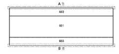
도 6은 수직구조 발광다이오드 소자를 제조하는 단계로서, 샌드위치 복합체를 형성하기 전에 준비된 기계 가공된 전기전도성 히트씽크 지지대부를 보인 단면도이다.6 is a cross-sectional view of a machined electro-conductive heat sink support lobe prepared prior to forming a sandwich composite, the step of fabricating a vertically structured light emitting diode device.
이에 도시된 바와 같이, 도 6은 기계 가공된 전기전도성 히트씽크 지지대(601)의 상하면에 전도성 웨이퍼 결합층(602, 603)이 형성된다. 여기서, 기계 가공된 전기전도성 상기 히트씽크 지지대(601)의 상면인 A면은 발광구조체가 성장된 성장기판이 결합되는 면이고, 대향하는 하면인 B면은 임시 기판인 웨이퍼 플레이트가 결합하는 면이다.6, the conductive wafer bonding layers 602 and 603 are formed on the upper and lower surfaces of the machined electro-conductive
상기 기계 가공된 전기전도성 히트씽크 지지대(601)는 5 μm 내지 1 mm 이하의 두께를 갖는 판(sheet), 디스크(disk), 또는 호일(foil) 형상을 갖는다.The machined electro-conductive
또한, 상기 기계 가공된 전기전도성 히트씽크 지지대(601)는 우수한 열 및 전기전도도를 갖는 물질이면 어떠한 물질이라도 사용에 제한하지 않는다. 특히, 상하면이 기계 가공된 Si, SiGe, ZnO, GaN, AlSiC, GaAs 기판, 그리고 Cu, Ni, Ag, Al, Nb, Ta, Ti, Au, Pd, Pd, W 성분들 중 적어도 하나 이상으로 이루어지는 금속, 합금, 또는 고용체를 사용하는 바람직하다.Further, the machined electro-conductive
상기 제1 전도성 웨이퍼 결합층(602), 제2 전도성 웨이퍼 결합층(603)은 일정 압력과 최소 300℃ 이상의 온도 조건하에서 치밀한 접착력을 형성하는 Au, Ni, Cu, Ti, Ag, Al, Si, Ge, Pt, Pd, Rh, W, Mo, V, Sc, Hf, Ir, Re, Co, Zr, Ru, Ta, Nb, Mn, Mn, Cr, 희토류금속 중 적어도 하나 이상을 포함하고 있는 금속, 합금, 고용체, 화합물이 사용되며, 특히 단층 또는 이중층 이상의 다층 구조로 이루어진다.The first conductive
도 7은 수직구조 발광다이오드 소자를 제조하는 단계로서, 샌드위치 복합체를 형성하기 전에 준비된 임시 기판인 웨이퍼 플레이트부를 보인 단면도이다.7 is a cross-sectional view showing a wafer plate portion which is a temporary substrate prepared before forming the sandwich composite, in the step of producing a vertically-structured light-emitting diode device.
이에 도시된 바와 같이, 도 7은 임시 기판인 웨이퍼 플레이트(701) 상면에 희생분리층(702)과 제2 전도성 웨이퍼 결합층(703)이 순차적으로 형성된다. 여기서, 상기 웨이퍼 플레이트(701)는 상기 발광구조체의 성정기판(501)과 동일 물질을 우선적으로 사용하되, 상기 성장기판(501)과의 열팽창계수 차이가 2ppm/℃ 이하를 갖는 물질계이면 어떠한 물질이라도 사용에 제한하지 않는다.7, the
또한, 상기 웨이퍼 플레이트(701) 상면에 형성되는 희생분리층(702)은 ZnO을 포함한 2-6족 화합물, GaN을 포함한 3-5족 화합물, Al, Au, Ag, Cr, Ti, ITO, PZT, SU-8 등을 포함한 각종 금속, 합금, 유기물로 구성된다.The
상기 제2 전도성 웨이퍼 결합층(703)은 일정 압력과 300℃ 이상의 온도 조건하에서 치밀한 접착력을 형성하는 Au, Ni, Cu, Ti, Ag, Al, Si, Ge, Pt, Pd, Rh, W, Mo, V, Sc, Hf, Ir, Re, Co, Zr, Ru, Ta, Nb, Mn, Mn, Cr, 희토류금속 중 적어도 하나 이상을 포함하고 있는 금속, 합금, 고용체, 화합물이 사용되며, 특히 단층 또는 이중층 이상의 다층 구조로 이루어진다.The second conductive
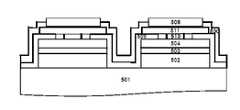
도 8은 수직구조 발광다이오드 소자를 제조하는 단계로서, 성장기판부, 히트씽크 지지대부, 및 웨이퍼 플레이트부를 동시에 웨이퍼 결합시킨 샌드위치 복합체의 단면도이다.8 is a cross-sectional view of a sandwich composite in which a growth plate, a heat sink support, and a wafer plate are simultaneously wafer bonded to produce a vertical structure light emitting diode device.
상기 성장기판부(A)는 성장기판(501) 상면에 n형 질화물계 클래드층(502), 질화물계 활성층(503), p형 질화물계 클래드층(504), p형 오믹접촉 전극층(510), 제1 소자 패시베이션층(509), 반사성 오믹접촉 전극층(511), 제1 전도성 웨이퍼 결합층(508) 적층되어 있다.The growth substrate portion A includes an n-type nitride-based
상기 히트씽크 지지대부(B)는 히트씽크 지지대(601)의 상하면에 각각 제1 및 제2 전도성 웨이퍼 결합층(602, 603)이 적층되어 있다.First and second conductive wafer bonding layers 602 and 603 are stacked on the upper and lower surfaces of the
상기 웨이퍼 플레이트부(C)는 임시 기판인 웨이퍼 플레이트(701) 상면에 희생분리층(702) 및 제2 전도성 웨이퍼 결합층(703)이 순차적으로 적층되어 있다.The wafer plate portion C includes a
상기 성장기판부(A), 히트씽크 지지대부(B), 및 웨이퍼 플레이트부(C)의 결합은 각각 제1 전도성 웨이퍼 결합층 간(508/602) 및 제2 전도성 웨이퍼 결합층 간(603/703)의 접합을 통해 일정 압력과 300℃ 이상의 온도에서 수행한다.The bonding of the growth plate portion A, the heat sink support portion B and the wafer plate portion C is performed between the first conductive
여기서, 웨이퍼 결합의 공정 개스 분위기는 진공, 질소(N2), 아르곤(Ar) 기체가 바람직하나, 경우에 따라서는 산소(O2) 기체가 첨가될 수도 있다.Here, the atmosphere of the process gas for wafer bonding is preferably vacuum, nitrogen (N 2), or argon (Ar) gas, but oxygen (O 2) gas may be added in some cases.
도 9는 수직구조 발광다이오드 소자를 제조하는 단계로서, 웨이퍼 결합된 샌드위치 복합체로부터 성장기판을 분리시키는 공정을 보인 단면도이다.9 is a cross-sectional view illustrating a process of separating a growth substrate from a wafer bonded sandwich composite, in the manufacture of a vertical structure light emitting diode device.
상기 성장기판(501)을 발광구조체로부터 분리하는 공정 기술은 엑사이머 레이저(excimer laser) 등을 이용한 레이저 리프트 오프(laser lift-off)의 방식으로 할 수도 있으며, 건식 및 습식 식각 방법으로 할 수도 있다. 특히, 상기 성장기판(501)이 사파이어와 SiC인 경우는 레이저 리프트 오프 방식으로 수행하는 것이 바람직하다. 즉, 상기 성장기판(501)에 일정 영역의 파장을 가지는 엑사이머 레이 저빔을 포커싱(focusing)하여 조사하면, 상기 성장기판(501)과 상기 완충층을 포함한 n형 질화물계 클래드층(502)의 경계면에 열에너지가 집중되어 상기 완충층을 포함한 n형 질화물 반도체(502)의 계면이 갈륨(gallium, Ga)과 질소(nitrogen, N) 분자로 열-화학적 분해가 발생하면서 레이저빔이 지나가는 부분에서 순간적으로 성장기판(501)의 분리가 일어난다.The process for separating the
도 10은 수직구조 발광다이오드 소자를 제조하는 단계로서, 성장기판이 분리된 후에 제2 소자 패시베이션층을 형성하는 공정을 보인 단면도이다.10 is a cross-sectional view showing a step of forming a second device passivation layer after a growth substrate is separated, in the step of manufacturing a vertical structure light emitting diode device.
상기 제2 소자 패시베이션층(512)은 대기에 노출된 n형 질화물계 클래드층(502) 상면과 제1 소자 패시베이션층(509), p형 오믹접촉 전극층(510), 반사성 오믹접촉 전극층(511), 및 제1 전도성 웨이퍼 결합층(508)의 측면 또는 상면에 형성된다.The second passivation layer 512 includes a
또한, 상기 제2 소자 패시베이션층(512)으로는 실리콘 산화박막(SiO2), 실리콘 질화박막(SiNx), 알루미늄 산화박막(Al2O3) 등이 사용되며, 상기 제2 소자 패시베이션층(512)은 100 ~ 1000㎚의 두께로 형성하는 것이 바람직하다.The second passivation layer 512 may be formed of a silicon oxide thin film (SiO2), a silicon nitride thin film (SiNx), an aluminum oxide thin film (Al2O3) It is preferable to form it to a thickness of 1000 nm.
도 11은 수직구조 발광다이오드 소자를 제조하는 단계로서, 제2 소자 패시베이션층의 일부 영역을 제거한 후에 대기에 노출된 n형 질화물계 클래드층 상면에 표면 요철을 형성하는 공정을 보인 단면도이다.11 is a cross-sectional view showing a step of forming surface irregularities on the upper surface of the n-type nitride-based clad layer exposed to the atmosphere after removing a part of the second device passivation layer, in the step of producing a vertical structure light emitting diode device.
상기 n형 질화물계 클래드층(502) 상면에 존재하는 소자 패시베이션층(800) 일부 영역을 제거시킨 후, 상기 n형 질화물계 클래드층(502) 상면에 구조적인 모양을 만드는 표면 요철(900)을 도입한다. 이러한 표면 요철(900) 도입은 상기 질화물 계 활성층(503)에서 생성된 빛을 외부로 방출시키는데 큰 도움을 주어, 수직구조 발광다이오드 소자의 외부 발광 효율을 상당히 개선할 수 있다.A part of the
여기서, 표면 요철(900) 도입은 습식 용액을 이용하여 일정한 규칙성이 없는 패턴을 형성하거나, 각종 리소그래피(lithography) 공정으로 패턴을 형성한 후에 식각 공정을 통하여 칩의 표면에 굴곡을 형성하는 방법을 사용하고 있다.Here, the introduction of the
도 12는 수직구조 발광다이오드 소자를 제조하는 단계로서, 표면 요철이 형성된 n형 질화물계 클래드층 상면에 n형 오믹접촉 전극구조체을 형성하는 공정을 보인 단면도이다.12 is a cross-sectional view showing a step of forming an n-type ohmic contact electrode structure on the upper surface of an n-type nitride-based clad layer on which surface irregularities are formed, in the step of producing a vertical structure light emitting diode device.
상기 표면 요철(900)이 도입된 n형 질화물계 클래드층(502) 상면에 n형 오믹접촉 전극구조체(1000)를 형성한다. 여기서, n형 오믹접촉 전극구조체(1000) 형성은 마스크를 이용하여 일부 영역 또는 전체 영역에 형성된다. 특히, 상기 n형 질화물계 클래드층(502) 상면에 형성된 n형 오믹접촉 전극구조체(1000)의 위치는 상기 p형 오믹접촉 전극층(510) 내의 커런트 블라킹 영역에 대향 되게 한다.The n-type ohmic
도 13은 수직구조 발광다이오드 소자를 제조하는 단계로서, 수직방향으로 절단하는 공정을 보인 단면도이다.FIG. 13 is a cross-sectional view showing a step of vertically cutting a step of manufacturing a vertically-structured light-emitting diode device.
완전하게 단일화시킨 수직구조 발광다이오드 소자를 제조하기 위해서 제1 전도성 웨이퍼 결합층(602), 히트씽크 지지대(601), 제2 전도성 웨이퍼 결합층(603, 703), 희생분리층(702)을 수직방향으로 모두 절단(1100) 한다. 여기서, 상기 임시 기판인 웨이퍼 플레이트(701)가 대기에 노출될 때까지 수행한다.The first conductive
도 14는 수직구조 발광다이오드 소자를 제조하는 마지막 단계로서, 상기 임 시 기판인 웨이퍼 플레이트로부터 수직구조 발광다이오드 소자를 분리한 후, 히트씽크 지지대 후면에 p형 오믹접촉 전극구체 및 다이 결합층을 형성시킨 단면도이다.FIG. 14 is a final step of manufacturing a vertical structure light emitting diode device. Referring to FIG. 14, a vertically-structured light emitting diode device is separated from a wafer plate as a temporary substrate, and a p-type ohmic contact electrode is formed on the back surface of the heat sink support. Respectively.
상기 임시 기판인 웨이퍼 플레이트(701)로부터 단일화시킨 다수개의 수직구조 발광다이오드 소자를 분리(lift-off)한 후, 상기 임시 기판인 히트씽크 지지대(601) 후면에 p형 오믹접촉 전극구체(1200)와 다이 결합층(1300)을 형성한다. 상기 임시 기판인 웨이퍼 플레이트(701)를 분리하는 공정은 강한 에너지를 갖춘 레이저빔을 이용한 열-화학 분해, 습식 식각, 또는 화학-기계적 폴리싱(CMP), 기계적 연마(polishing) 등을 이용한다.The p-type ohmic
도 15 내지 23은 본 발명에 따른 제2 실시예로서, 수직구조 발광다이오드 소자 제조 공정을 보인 단면도이다.15 to 23 are cross-sectional views illustrating a vertical structure light emitting diode device manufacturing process according to a second embodiment of the present invention.
도 15는 수직구조 발광다이오드 소자를 제조하는 첫 번째 단계로서, 샌드위치 복합체를 형성하기 전에 준비된 성장기판부를 보인 단면도이다.15 is a cross-sectional view showing a growth plate prepared before the formation of the sandwich composite, as a first step in fabricating the vertical structure light emitting diode device.
이에 도시된 바와 같이, 성장기판(501) 상면에 완충층을 포함한 n형 질화물계 클래드층(502), 질화물계 활성층(503), p형 질화물계 클래드층(504)을 순차적으로 성장한 다음에 섬화 공정을 수행하고, 상기 p형 질화물계 클래드층(504) 상면에 p형 오믹접촉 전극층(510)과 제1 소자 패시베이션층(509) 적층한다. 다음으로, 상기 p형 오믹접촉 전극층(510)과 제1 소자 패시베이션층(509) 상면에 반사성 오믹접촉 전극층(511)을 적층한 다음, 연이어 상기 제1 소자 패시베이션층(509)과 반사성 오믹접촉 전극층(511) 상면 또는 측면에 제2 소자 패시베이션층(800)을 형성한다.As shown, an n-type nitride-based
그런 후, 상기 제2 소자 패시베이션층(800)의 일부 영역을 제거한 후에 상기 반사성 오믹접촉 전극층(511) 상면에 제1 전도성 웨이퍼 결합층(508)을 형성한다.Thereafter, a first conductive
여기서, 상기 성장기판(501)으로는 사파이어(Al2O3), 실리콘 카바이드(SiC), 실리콘(Si), 갈륨아세나이드(GaAs), 질화알루미늄(AlN), 질화갈륨(GaN), 질화알루미늄갈륨(AlGaN), 유리(glass) 등을 사용하며, 특히 사파이어 기판이 대표적으로 사용되는데, 이는 상기 성장기판(501)상면에 성장되는 그룹 3족 질화물계 반도체 물질의 결정 구조와 동일하면서 격자 정합을 이루는 상업적인 기판이 존재하지 않기 때문이다.The
상기 성장기판(501) 상면에 성장된 n형 질화물계 클래드층(502)은 AlxInyGa(1-x-y)N 조성식 (여기서, 0≤x≤1, 0≤y≤1, 0≤x+y≤1)을 갖는 n형 도판트(dopant)가 첨가된 그룹 3족 질화물계 반도체 물질로 이루어질 수 있으며, 특히 GaN가 널리 사용된다. 또한 상기 n형 질화물계 클래드층(502)을 성장하기에 앞서 불일치한 격자 정합 및 열팽창 계수 차이로 발생되는 스트레스를 완화시키는 물질층(“완충층” 으로 지칭)을 삽입될 수 있으며, 특히 GaN, AlN, InGaN, AlGaN, SiC, SiCN가 널리 사용된다.The n-type nitride-based
상기 n형 질화물계 클래드층(502) 상면에 형성되는 질화물계 활성층(503)은 양자 우물(Quantum Well) 구조를 가지며, AlxInyGa(1-x-y)N 조성식 (여기서, 0≤x≤1, 0≤y≤1, 0≤x+y≤1)을 갖는 그룹 3족 질화물계 반도체 물질계로 이루어진다.The nitride-based
상기 질화물계 활성층(503) 상면에 형성되는 p형 질화물계 클래드층(504)은 상기 n형 질화물계 클래드층(502)과 마찬가지로, AlxInyGa(1-x-y)N 조성식 (여기 서, 0≤x≤1, 0≤y≤1, 0≤x+y≤1)을 갖는 그룹 3족 질화물계 반도체 물질로 이루어지며, p형 도판트가 첨가된다.The p-type nitride-based
상기 p형 질화물계 클래드층(504)은 표면 개질층(interface modification layer)을 별도로 포함할 있다. 상기 표면 개질층은 슈퍼래티스 구조(spuerlattice structure), n형 도전성의 InGaN, GaN, AlInN, AlN, InN, AlGaN, p형 도전성의 InGaN, AlInN, InN, AlGaN, 또는 질소 극성으로 형성된 표면(nitrogen-polar surface)을 갖는 그룹 3족 질화물계이다. 특히, 상기 슈퍼래티스 구조의 표면 개질층은 그룹 2족, 3족, 또는 4족 원소 성분을 포함하고 있는 질화물(nitride) 또는 탄소질화물(carbon nitride)로 구성된다.The p-type nitride-based
여기서, 상기 n형 질화물계 클래드층(502), 질화물계 활성층(503), p형 질화물계 클래드층(504)은 MOCVD(Metal Organic Chemical Vapor Deposition)법 또는 MBE(Molecular Beam Epitaxy)법 등과 같은 증착 공정을 사용하여 성장시키되, 특히 MOCVD법으로 성장시키는 것이 바람직하다.The n-type nitride-based
상기 p형 오믹접촉 전극층(510)은 p형 질화물계 클래드층(504) 상면에서 오믹접촉 계면을 형성하고 있는 동시에 커런트 브라킹 영역을 포함하고 있다. 여기서, 상기 커런트 블라킹 영역은 대기(air) 상태 또는 전기절연성 물질, 또는 상기 p형 질화물계 클래드층과 쇼키접촉 계면을 형성하는 물질로 구성된다.The p-type ohmic
상기 제1 소자 패시베이션층(509)은 상기 p형 질화물계 클래드층(402) 상면과 메사 식각된 측면에 형성한다.The
또한, 상기 제1 소자 패시베이션층(509)으로는 실리콘 산화박막(SiO2), 실리 콘 질화박막(SiNx), 알루미늄 산화박막(Al2O3) 등이 사용되며, 상기 제1 소자 패시베이션층(509)은 10 ~ 100㎚의 두께로 형성하는 것이 바람직하다.The
상기 반사성 오믹접촉 전극층(511)은 p형 오믹접촉 전극층(510)과 상기 제1 소자 패시베이션층(509) 상면에 형성되며, 이를 구성하는 물질은 니켈(Ni), Ni 관련 합금 및 고용체, 은(Ag), Ag 관련 합금 및 고용체, 알루미늄(Al), Al 관련 합금 및 고용체, 로듐(Rh), Rh 관련 합금 및 고용체, 백금(Pt), Pt 관련 합금 및 고용체, 팔라듐(Pd), Pd 관련 합금 및 고용체, 금(Au), Au 관련 합금 및 고용체, Ag-Si, Al-Si, Rh-Si, Pd-Si, Ni-Si, Cr-Si, Pt-Si 등의 각종 실리사이드(silicide)이다.The reflective ohmic
또한, 상기 반사성 오믹접촉 전극층(511)은 소정의 면적을 갖는 p형 오믹접촉 전극층(510)보다 더 넓게 형성한다.In addition, the reflective ohmic
상기 제2 소자 패시베이션층(800)은 제1 소자 패시베이션층(509)과 반사성 오믹접촉 전극층(511) 상면 또는 측면에 형성한다.The
또한, 상기 제2 소자 패시베이션층(800)으로는 실리콘 산화박막(SiO2), 실리콘 질화박막(SiNx), 알루미늄 산화박막(Al2O3) 등이 사용되며, 상기 제2 소자 패시베이션층(800)은 100 ~ 1000㎚의 두께로 형성하는 것이 바람직하다.The
상기 제1 전도성 웨이퍼 결합층(508)은 상기 반사성 오믹접촉 전극층(511) 상면의 일부 영역에 일정 압력과 최소 300℃ 이상의 온도 조건하에서 치밀한 접착력을 형성하는 Au, Ni, Cu, Ti, Ag, Al, Si, Ge, Pt, Pd, Rh, W, Mo, V, Sc, Hf, Ir, Re, Co, Zr, Ru, Ta, Nb, Mn, Mn, Cr, 희토류금속 중 적어도 하나 이상을 포함 하고 있는 금속, 합금, 고용체, 화합물이 사용되며, 특히 단층 또는 이중층 이상의 다층 구조로 이루어진다.The first conductive
도 16은 수직구조 발광다이오드 소자를 제조하는 단계로서, 샌드위치 복합체를 형성하기 전에 준비된 기계 가공된 전기전도성 히트씽크 지지대부를 보인 단면도이다.16 is a cross-sectional view of a machined electroconductive heat sink support prepared prior to forming a sandwich composite, the step of fabricating a vertically structured light emitting diode device.
이에 도시된 바와 같이, 도 16은 기계 가공된 전기전도성 히트씽크 지지대(601)의 상하면에 전도성 웨이퍼 결합층(602, 603)이 형성된다. 여기서, 기계 가공된 전기전도성 상기 히트씽크 지지대(601)의 상면인 A면은 발광구조체가 성장된 성장기판이 결합되는 면이고, 대향하는 하면인 B면은 임시 기판인 웨이퍼 플레이트가 결합하는 면이다.16, the conductive wafer bonding layers 602 and 603 are formed on the upper and lower surfaces of the machined electro-conductive
상기 기계 가공된 전기전도성 히트씽크 지지대(601)는 5 μm 내지 1 mm 이하의 두께를 갖는 판(sheet), 디스크(disk), 또는 호일(foil) 형상을 갖는다.The machined electro-conductive
또한, 상기 기계 가공된 전기전도성 지지대(601)는 우수한 열 및 전기전도도를 갖는 물질이면 어떠한 물질이라도 사용에 제한하지 않는다. 특히, 상하면이 기계 가공된 Si, SiGe, ZnO, GaN, AlSiC, GaAs 기판, 그리고 Cu, Ni, Ag, Al, Nb, Ta, Ti, Au, Pd, Pd, W 성분들 중 적어도 하나 이상으로 이루어지는 금속, 합금, 또는 고용체를 사용하는 바람직하다.In addition, the machined
상기 제1 전도성 웨이퍼 결합층(602), 제2 전도성 웨이퍼 결합층(603)은 일정 압력과 최소 300℃ 이상의 온도 조건하에서 치밀한 접착력을 형성하는 Au, Ni, Cu, Ti, Ag, Al, Si, Ge, Pt, Pd, Rh, W, Mo, V, Sc, Hf, Ir, Re, Co, Zr, Ru, Ta, Nb, Mn, Mn, Cr, 희토류금속 중 적어도 하나 이상을 포함하고 있는 금속, 합금, 고용체, 화합물이 사용되며, 특히 단층 또는 이중층 이상의 다층 구조로 이루어진다.The first conductive
도 17은 수직구조 발광다이오드 소자를 제조하는 단계로서, 샌드위치 복합체를 형성하기 전에 준비된 임시 기판인 웨이퍼 플레이트부를 보인 단면도이다.17 is a cross-sectional view showing a wafer plate portion which is a provisional substrate prepared before forming the sandwich composite, which is a step of manufacturing a vertical structure light emitting diode device.
이에 도시된 바와 같이, 도 17은 임시 기판인 웨이퍼 플레이트(701) 상면에 희생분리층(702)과 제2 전도성 웨이퍼 결합층(703)이 순차적으로 형성된다. 여기서, 상기 웨이퍼 플레이트(701)는 상기 발광구조체의 성정기판(501)과 동일 물질을 우선적으로 사용하되, 상기 성장기판(501)과의 열팽창계수 차이가 2ppm/℃ 이하를 갖는 물질계이면 어떠한 물질이라도 사용에 제한하지 않는다.17, a
또한, 상기 웨이퍼 플레이트(701) 상면에 형성되는 희생분리층(702)은 ZnO을 포함한 2-6족 화합물, GaN을 포함한 3-5족 화합물, Al, Au, Ag, Cr, Ti, ITO, PZT, SU-8 등을 포함한 각종 금속, 합금, 유기물로 구성된다.The
상기 제2 전도성 웨이퍼 결합층(703)은 일정 압력과 300℃ 이상의 온도 조건하에서 치밀한 접착력을 형성하는 Au, Ni, Cu, Ti, Ag, Al, Si, Ge, Pt, Pd, Rh, W, Mo, V, Sc, Hf, Ir, Re, Co, Zr, Ru, Ta, Nb, Mn, Mn, Cr, 희토류금속 중 적어도 하나 이상을 포함하고 있는 금속, 합금, 고용체, 화합물이 사용되며, 특히 단층 또는 이중층 이상의 다층 구조로 이루어진다.The second conductive
도 18은 수직구조 발광다이오드 소자를 제조하는 단계로서, 성장기판부, 히트씽크 지지대부, 및 웨이퍼 플레이트부를 동시에 웨이퍼 결합시킨 샌드위치 복합체의 단면도이다.18 is a cross-sectional view of a sandwich composite in which a growth substrate, a heat sink support, and a wafer plate are simultaneously wafer bonded to produce a vertical structure light emitting diode device.
상기 성장기판부(D)는 성장기판(501) 상면에 n형 질화물계 클래드층(502), 질화물계 활성층(503), p형 질화물계 클래드층(504), p형 오믹접촉 전극층(510), 제1 소자 패시베이션층(509), 반사성 오믹접촉 전극층(511), 제1 전도성 웨이퍼 결합층(508) 적층되어 있다.The growth substrate section D includes an n-type nitride-based
상기 히트씽크 지지대부(E)는 히트씽크 지지대(601)의 상하면에 각각 제1 및 제2 전도성 웨이퍼 결합층(602, 603)이 적층되어 있다.First and second conductive wafer bonding layers 602 and 603 are stacked on the top and bottom surfaces of the
상기 웨이퍼 플레이트부(F)는 임시 기판인 웨이퍼 플레이트(701) 상면에 희생분리층(702) 및 제2 전도성 웨이퍼 결합층(703)이 순차적으로 적층되어 있다.The wafer plate portion F includes a
상기 성장기판부(D), 히트씽크 지지대부(E), 및 웨이퍼 플레이트부(F)의 결합은 각각 제1 전도성 웨이퍼 결합층 간(508/602) 및 제2 전도성 웨이퍼 결합층 간(603/703)의 접합을 통해 일정 압력과 300℃ 이상의 온도에서 수행한다.The bonding of the growth plate portion D, the heat sink support portion E and the wafer plate portion F is performed between the first conductive
여기서, 웨이퍼 결합의 공정 개스 분위기는 진공, 질소(N2), 아르곤(Ar) 기체가 바람직하나, 경우에 따라서는 산소(O2) 기체가 첨가될 수도 있다.Here, the atmosphere of the process gas for wafer bonding is preferably vacuum, nitrogen (N 2), or argon (Ar) gas, but oxygen (O 2) gas may be added in some cases.
도 19는 수직구조 발광다이오드 소자를 제조하는 단계로서, 웨이퍼 결합된 샌드위치 복합체로부터 성장기판을 분리시키는 공정을 보인 단면도이다.19 is a cross-sectional view illustrating a process of separating a growth substrate from a wafer bonded sandwich composite, which is a step of fabricating a vertically structured light emitting diode device.
상기 성장기판(501)을 발광구조체로부터 분리하는 공정 기술은 엑사이머 레이저(excimer laser) 등을 이용한 레이저 리프트 오프(laser lift-off)의 방식으로 할 수도 있으며, 건식 및 습식 식각의 방법으로 할 수도 있다. 특히, 상기 성장기판(501)이 사파이어와 SiC인 경우는 레이저 리프트 오프 방식으로 수행하는 것이 바람직하다. 즉, 상기 성장기판(501)에 일정 영역의 파장을 가지는 엑사이머 레이 저빔을 포커싱(focusing)하여 조사하면, 상기 성장기판(501)과 상기 완충층을 포함한 n형 질화물계 클래드층(502)의 경계면에 열에너지가 집중되어 상기 완충층을 포함한 n형 질화물 반도체(502)의 계면이 갈륨(gallium, Ga)과 질소(nitrogen, N) 분자로 열-화학적 분해가 발생하면서 레이저빔이 지나가는 부분에서 순간적으로 성장기판(501)의 분리가 일어난다.The process for separating the
도 20은 수직구조 발광다이오드 소자를 제조하는 단계로서, 대기에 노출된 n형 질화물계 클래드층 상면에 표면 요철을 형성하는 공정을 보인 단면도이다.20 is a cross-sectional view showing a step of forming surface irregularities on the upper surface of the n-type nitride-based clad layer exposed to the atmosphere, in the step of producing a vertically-structured light-emitting diode device.
상기 대기에 노출된 n형 질화물계 클래드층(502) 상면에 구조적인 모양을 만드는 표면 요철(900)을 도입한다. 이러한 표면 요철(900) 도입은 상기 질화물계 활성층(503)에서 생성된 빛을 외부로 방출시키는데 큰 도움을 주어, 수직구조 발광다이오드 소자의 외부 발광 효율을 상당히 개선할 수 있다.The
여기서, 표면 요철(900) 도입은 습식 용액을 이용하여 일정한 규칙성이 없는 패턴을 형성하거나, 각종 리소그래피(lithography) 공정으로 패턴을 형성한 후에 식각 공정을 통하여 칩의 표면에 굴곡을 형성하는 방법을 사용하고 있다.Here, the introduction of the
도 21은 수직구조 발광다이오드 소자를 제조하는 단계로서, 표면 요철이 형성된 n형 질화물계 클래드층 상면에 n형 오믹접촉 전극구조체을 형성하는 공정을 보인 단면도이다.21 is a cross-sectional view showing a step of forming an n-type ohmic contact electrode structure on the top surface of an n-type nitride-based clad layer on which surface irregularities are formed, in the step of producing a vertical structure light emitting diode device.
상기 표면 요철(900)이 도입된 n형 질화물계 클래드층(502) 상면에 n형 오믹접촉 전극구조체(1000)를 형성한다. 여기서, n형 오믹접촉 전극구조체(1000) 형성은 마스크를 이용하여 일부 영역 또는 전체 영역에 형성된다. 특히, 상기 n형 질화 물계 클래드층(502) 상면에 형성된 n형 오믹접촉 전극구조체(1000)의 위치는 상기 p형 오믹접촉 전극층(510) 내의 커런트 블라킹 영역에 대향 되게 한다.The n-type ohmic
도 22는 수직구조 발광다이오드 소자를 제조하는 단계로서, 수직방향으로 절단하는 공정을 보인 단면도이다.22 is a cross-sectional view showing a step of cutting in a vertical direction in a step of manufacturing a vertically-structured light-emitting diode device.
완전하게 단일화시킨 수직구조 발광다이오드 소자를 제조하기 위해서 제1 전도성 웨이퍼 결합층(602), 히트씽크 지지대(601), 제2 전도성 웨이퍼 결합층(603, 703), 희생분리층(702)을 수직방향으로 모두 절단(1100) 한다. 여기서, 상기 임시 기판인 웨이퍼 플레이트(701)가 대기에 노출될 때까지 수행한다.The first conductive
도 23은 수직구조 발광다이오드 소자를 제조하는 마지막 단계로서, 상기 임시 기판인 웨이퍼 플레이트로부터 수직구조 발광다이오드 소자를 분리한 후, 히트씽크 지지대 후면에 p형 오믹접촉 전극구체 및 다이 결합층을 형성시킨 단면도이다.FIG. 23 is a final step of manufacturing a vertical structure light emitting diode device. Referring to FIG. 23, a vertical structure light emitting diode device is separated from a wafer plate serving as the temporary substrate, and then a p-type ohmic contact electrode and a die bonding layer are formed on the back surface of the heat sink support Sectional view.
상기 임시 기판인 웨이퍼 플레이트(701)로부터 단일화시킨 다수개의 수직구조 발광다이오드 소자를 분리(lift-off)한 후, 상기 임시 기판인 히트씽크 지지대(601) 후면에 p형 오믹접촉 전극구체(1200)와 다이 결합층(1300)을 형성한다. 상기 임시 기판인 웨이퍼 플레이트(701)를 분리하는 공정은 강한 에너지를 갖춘 레이저빔을 이용한 열-화학 분해, 습식 식각, 또는 화학-기계적 폴리싱(CMP), 기계적 연마(polishing) 등을 이용한다.The p-type ohmic
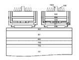
도 24는 본 발명에 따라 제조된 단결정 그룹 3족 질화물계 반도체을 이용한 수직구조 발광다이오드 소자를 보인 단면도이다.24 is a cross-sectional view showing a vertical structure light emitting diode device using a single crystal group III nitride based semiconductor manufactured according to the present invention.
도 24A를 참조하면, 기계 가공된 전기전도성 히트씽크 지지대(601) 상면에 두층의 전도성 웨이퍼 결합층(508, 602)에 의해 구조적 및 전기적으로 연결된 발광다이오드 소자용 발광구조체가 형성되어 되어 있다. 여기서, 상기 발광구조체의 p형 질화물계 클래드층(504)과 두층의 전도성 웨이퍼 결합층(508, 602) 사이에 p형 오믹접촉 전극층(510)과 반사성 오믹접촉 전극층(511)을 형성하고 있어, 전기 및 광학적으로 우수한 수직구조 발광다이오드 소자를 제조할 수 있다. 더 나아가서, 상기 p형 오믹접촉 전극층(410)은 커런트 블라킹 영역을 포함하고 있어, n형 오믹접촉 전극구조체(1000)와, 다이 결합층(1300)과 연결된 p형 오믹접촉 전극구조체(1200)를 통해서 외부 전류 주입 시에 상기 n형 오익접촉 전극구조체(1000) 주위에 전류 집중 현상을 회피할 수 있다.Referring to FIG. 24A, a light emitting structure for a light emitting diode device structured and electrically connected by two layers of conductive wafer bonding layers 508 and 602 is formed on the upper surface of a machined electro-conductive
또한, 두층의 소자 패시베이션층(509, 800)에 의해서 상기 발광구조체를 외부의 도전성 물질 및 수분으로부터 완전하게 보호하기 때문에 높은 소자 신뢰성을 확보할 수 있다. 특히, 상기 제2 소자 패시베이션층(800)은 히트씽크 지지대(601) 상면에 있는 제1 전도성 웨이퍼 결합층(602)과 접촉하고 있는 것이 특징이다.In addition, since the light emitting structure is completely protected from the external conductive material and moisture by the two device passivation layers 509 and 800, high device reliability can be ensured. Particularly, the second
또 다른 본 발명에 의해 제조된 수직구조 발광다이오드 소자로서, 도 24B를 참조하면, 기계 가공된 전기전도성 히트씽크 지지대(601) 상면에 두층의 전도성 웨이퍼 결합층(508, 602)에 의해 구조적 및 전기적으로 연결된 발광다이오드 소자용 발광구조체가 형성되어 되어 있다. 여기서, 상기 발광구조체의 p형 질화물계 클래드층(504)과 두층의 전도성 웨이퍼 결합층(508, 602) 사이에 p형 오믹접촉 전극층(510)과 반사성 오믹접촉 전극층(511)을 형성하고 있어, 전기 및 광학적으로 우 수한 수직구조 발광다이오드 소자를 제조할 수 있다. 더 나아가서, 상기 p형 오믹접촉 전극층(410)은 커런트 블라킹 영역을 포함하고 있어, n형 오믹접촉 전극구조체(1000)와, 다이 결합층(1300)과 연결된 p형 오믹접촉 전극구조체(1200)를 통해서 외부 전류 주입 시에 상기 n형 오익접촉 전극구조체(1000) 주위에 전류 집중 현상을 회피할 수 있다.Referring to Fig. 24B, a vertically structured light emitting diode device manufactured according to another embodiment of the present invention includes two electrically conductive wafer bonding layers 508 and 602 on the upper surface of a machined electroconductive
또한, 두층의 소자 패시베이션층(509, 800)에 의해서 상기 발광구조체를 외부의 도전성 물질 및 수분으로부터 완전하게 보호하기 때문에 높은 소자 신뢰성을 확보할 수 있다. 특히, 상기 제2 소자 패시베이션층(800)은 히트씽크 지지대(601) 상면에 있는 제1 전도성 웨이퍼 결합층(602)과 덜어져 있는 것이 특징이다.In addition, since the light emitting structure is completely protected from the external conductive material and moisture by the two device passivation layers 509 and 800, high device reliability can be ensured. Particularly, the second
한편, 상기에서는 본 발명을 특정의 바람직한 실시예에 관련하여 도시하고 설명하였지만, 이하의 특허청구범위에 의해 마련되는 본 발명의 정신이나 분야를 이탈하지 않는 한도 내에서 본 발명이 다양하게 개조 및 변화될 수 있다는 것을 당업계에서 통상의 지식을 가진 자는 용이하게 알 수 있다.While the present invention has been particularly shown and described with reference to preferred embodiments thereof, it will be understood by those of ordinary skill in the art that various changes in form and details may be made therein without departing from the spirit and scope of the invention, It will be readily apparent to those skilled in the art.
도 1은 종래기술에 따라 단일화된 단위칩 형태의 그룹 3족 질화물계 수평구조의 발광다이오드 소자 도시한 단면도이고,FIG. 1 is a cross-sectional view of a group III nitride-based horizontal structure light emitting diode device in a unit chip form unified according to the prior art,
도 2는 종래기술에 따라 단일화된 단위칩 형태의 그룹 3족 질화물계 수직구조 발광다이오드 소자를 제조하는 공정을 도시한 도면도이고,FIG. 2 is a view showing a process for manufacturing a group III nitride-based vertical-structured light-emitting diode device in the unit chip form unified according to the related art,
도 3은 종래기술에 따라 단일화된 단위칩 형태의 그룹 3족 질화물계 수직구조 발광다이오드 소자를 제조하는 공정을 도시한 도면도이고,FIG. 3 is a view showing a process for manufacturing a group III nitride-based vertical-structured light-emitting diode device in the form of a single unit chip according to the related art,
도 4는 본 발명에 의해 제안된 웨이퍼 결합 공정을 통한 그룹 3족 질화물계 반도체를 이용한 수직구조 발광소자 제조에 관한 공정을 보인 개략적인 단면도이고,FIG. 4 is a schematic cross-sectional view showing a process for manufacturing a vertical structure light-emitting device using a group III nitride-based semiconductor through a wafer bonding process proposed by the present invention,
도 5 내지 14는 본 발명에 따른 제1 실시예로서, 수직구조 발광다이오드 소자 제조 공정을 보인 단면도이고,5 to 14 are cross-sectional views illustrating a vertical-type LED device manufacturing process according to a first embodiment of the present invention,
도 15 내지 23은 본 발명에 따른 제2 실시예로서, 수직구조 발광다이오드 소자 제조 공정을 보인 단면도이고,15 to 23 are cross-sectional views illustrating a vertical structure light emitting diode device manufacturing process according to a second embodiment of the present invention,
도 24는 본 발명에 따라 제조된 단결정 그룹 3족 질화물계 반도체를 이용한 수직구조 발광다이오드 소자를 보인 단면도이다.24 is a sectional view showing a vertical structure light emitting diode device using a single crystal group III nitride based semiconductor manufactured according to the present invention.
Claims (26)
Translated fromKoreanPriority Applications (6)
| Application Number | Priority Date | Filing Date | Title |
|---|---|---|---|
| KR1020080030919AKR101428066B1 (en) | 2008-04-02 | 2008-04-02 | vertical structured group 3 nitride-based light emitting diode and its fabrication methods |
| EP09754948.9AEP2262012B1 (en) | 2008-04-02 | 2009-04-02 | Light-emitting diode and a method of manufacturing thereof |
| CN200980119150.1ACN102106001B (en) | 2008-04-02 | 2009-04-02 | Light emitting device and manufacturing method thereof |
| JP2011502858AJP5220916B2 (en) | 2008-04-02 | 2009-04-02 | Light emitting device and manufacturing method thereof |
| PCT/KR2009/001710WO2009145483A2 (en) | 2008-04-02 | 2009-04-02 | Light-emitting element and a production method therefor |
| US12/936,090US8829554B2 (en) | 2008-04-02 | 2009-04-02 | Light emitting element and a production method therefor |
Applications Claiming Priority (1)
| Application Number | Priority Date | Filing Date | Title |
|---|---|---|---|
| KR1020080030919AKR101428066B1 (en) | 2008-04-02 | 2008-04-02 | vertical structured group 3 nitride-based light emitting diode and its fabrication methods |
Publications (2)
| Publication Number | Publication Date |
|---|---|
| KR20090105462A KR20090105462A (en) | 2009-10-07 |
| KR101428066B1true KR101428066B1 (en) | 2014-08-07 |
Family
ID=41535163
Family Applications (1)
| Application Number | Title | Priority Date | Filing Date |
|---|---|---|---|
| KR1020080030919AExpired - Fee RelatedKR101428066B1 (en) | 2008-04-02 | 2008-04-02 | vertical structured group 3 nitride-based light emitting diode and its fabrication methods |
Country Status (1)
| Country | Link |
|---|---|
| KR (1) | KR101428066B1 (en) |
Families Citing this family (7)
| Publication number | Priority date | Publication date | Assignee | Title |
|---|---|---|---|---|
| KR101658838B1 (en) | 2010-02-04 | 2016-10-04 | 엘지이노텍 주식회사 | Light emitting device and method for fabricating the same |
| KR101007137B1 (en) | 2010-03-08 | 2011-01-10 | 엘지이노텍 주식회사 | Light emitting device, light emitting device manufacturing method and light emitting device package |
| US11398581B2 (en) | 2017-11-02 | 2022-07-26 | Lg Innotek Co., Ltd. | Semiconductor device |
| KR102483533B1 (en)* | 2017-11-02 | 2023-01-02 | 엘지이노텍 주식회사 | Semiconductor device array and method of manufacturing semiconductor device array using the same |
| KR102051477B1 (en)* | 2018-02-26 | 2019-12-04 | 주식회사 세미콘라이트 | Method of manufacturing semiconductor light emitting device |
| KR20220057128A (en)* | 2020-10-29 | 2022-05-09 | 웨이브로드 주식회사 | Light emitting device and method of manufacturing the same |
| CN117790659B (en)* | 2024-02-26 | 2024-07-12 | 诺视科技(苏州)有限公司 | Micro-display luminous pixel with omnibearing reflecting mirror structure and its making method |
Citations (4)
| Publication number | Priority date | Publication date | Assignee | Title |
|---|---|---|---|---|
| JP2004281863A (en) | 2003-03-18 | 2004-10-07 | Nichia Chem Ind Ltd | Nitride semiconductor device and method of manufacturing the same |
| JP2006100500A (en) | 2004-09-29 | 2006-04-13 | Sanken Electric Co Ltd | Semiconductor light emitting device and manufacturing method thereof |
| KR20070038272A (en)* | 2005-10-05 | 2007-04-10 | 삼성전기주식회사 | Manufacturing method of vertical structure light emitting diode |
| JP2007335793A (en) | 2006-06-19 | 2007-12-27 | Sanken Electric Co Ltd | Semiconductor light emitting device and manufacturing method thereof |
- 2008
- 2008-04-02KRKR1020080030919Apatent/KR101428066B1/ennot_activeExpired - Fee Related
Patent Citations (4)
| Publication number | Priority date | Publication date | Assignee | Title |
|---|---|---|---|---|
| JP2004281863A (en) | 2003-03-18 | 2004-10-07 | Nichia Chem Ind Ltd | Nitride semiconductor device and method of manufacturing the same |
| JP2006100500A (en) | 2004-09-29 | 2006-04-13 | Sanken Electric Co Ltd | Semiconductor light emitting device and manufacturing method thereof |
| KR20070038272A (en)* | 2005-10-05 | 2007-04-10 | 삼성전기주식회사 | Manufacturing method of vertical structure light emitting diode |
| JP2007335793A (en) | 2006-06-19 | 2007-12-27 | Sanken Electric Co Ltd | Semiconductor light emitting device and manufacturing method thereof |
Also Published As
| Publication number | Publication date |
|---|---|
| KR20090105462A (en) | 2009-10-07 |
Similar Documents
| Publication | Publication Date | Title |
|---|---|---|
| KR101438818B1 (en) | light emitting diode | |
| JP5220916B2 (en) | Light emitting device and manufacturing method thereof | |
| US8946745B2 (en) | Supporting substrate for manufacturing vertically-structured semiconductor light-emitting device and semiconductor light-emitting device using the supporting substrate | |
| CN102047454B (en) | Light emitting device and manufacturing method thereof | |
| CN102106006B (en) | Support substrate for manufacturing semiconductor light emitting device and semiconductor light emitting device using support substrate | |
| KR101198758B1 (en) | Vertical structured semiconductor light emitting device and method for producing thereof | |
| US8791480B2 (en) | Light emitting device and manufacturing method thereof | |
| KR101470020B1 (en) | epitaxial semiconductor thin-film transfer using sandwich-structured wafer bonding and photon-beam | |
| KR101428066B1 (en) | vertical structured group 3 nitride-based light emitting diode and its fabrication methods | |
| KR100999548B1 (en) | A support substrate for manufacturing a semiconductor light emitting device having a vertical structure, a method for manufacturing a semiconductor light emitting device having a vertical structure and a semiconductor light emitting device having a vertical structure | |
| KR101510382B1 (en) | fabrication of vertical structured light emitting diodes using group 3 nitride-based semiconductors and its related methods | |
| KR101480551B1 (en) | vertical structured group 3 nitride-based light emitting diode and its fabrication methods | |
| KR100886110B1 (en) | Support substrate for semiconductor light emitting device and method for manufacturing semiconductor light emitting device having vertical structure using same | |
| KR20090116410A (en) | Light emitting device having vertical electrode structure and manufacturing method thereof | |
| KR101499954B1 (en) | fabrication of vertical structured light emitting diodes using group 3 nitride-based semiconductors and its related methods | |
| KR101231118B1 (en) | Supporting substrates for semiconductor light emitting device and high-performance vertical structured semiconductor light emitting devices using supporting substrates | |
| KR101534846B1 (en) | Group III nitride-based semiconductor light-emitting diode device with vertical structure and manufacturing method | |
| KR20070044099A (en) | Nitride Semiconductor Light Emitting Diode and Manufacturing Method Thereof | |
| KR20090115631A (en) | Group III-nitride semiconductor light emitting diode device of vertical structure and manufacturing method | |
| KR101526566B1 (en) | fabrication of vertical structured light emitting diodes using group 3 nitride-based semiconductors and its related methods | |
| KR101171855B1 (en) | Supporting substrates for semiconductor light emitting device and high-performance vertical structured semiconductor light emitting devices using supporting substrates | |
| KR20090112854A (en) | Group 3 nitride-based semiconductor light emitting diodes and methods to fabricate them | |
| KR101499953B1 (en) | Vertical structure group III nitride-based semiconductor light-emitting diode device and manufacturing method | |
| KR101550913B1 (en) | 3 fabrication of vertical structured light emitting diodes using group 3 nitride-based semiconductors and its related methods | |
| KR101681573B1 (en) | Method of manufacturing Light emitting device |
Legal Events
| Date | Code | Title | Description |
|---|---|---|---|
| PA0109 | Patent application | St.27 status event code:A-0-1-A10-A12-nap-PA0109 | |
| P22-X000 | Classification modified | St.27 status event code:A-2-2-P10-P22-nap-X000 | |
| PN2301 | Change of applicant | St.27 status event code:A-3-3-R10-R13-asn-PN2301 St.27 status event code:A-3-3-R10-R11-asn-PN2301 | |
| PG1501 | Laying open of application | St.27 status event code:A-1-1-Q10-Q12-nap-PG1501 | |
| N231 | Notification of change of applicant | ||
| PN2301 | Change of applicant | St.27 status event code:A-3-3-R10-R13-asn-PN2301 St.27 status event code:A-3-3-R10-R11-asn-PN2301 | |
| R17-X000 | Change to representative recorded | St.27 status event code:A-3-3-R10-R17-oth-X000 | |
| A201 | Request for examination | ||
| PA0201 | Request for examination | St.27 status event code:A-1-2-D10-D11-exm-PA0201 | |
| E902 | Notification of reason for refusal | ||
| PE0902 | Notice of grounds for rejection | St.27 status event code:A-1-2-D10-D21-exm-PE0902 | |
| E13-X000 | Pre-grant limitation requested | St.27 status event code:A-2-3-E10-E13-lim-X000 | |
| P11-X000 | Amendment of application requested | St.27 status event code:A-2-2-P10-P11-nap-X000 | |
| P13-X000 | Application amended | St.27 status event code:A-2-2-P10-P13-nap-X000 | |
| P22-X000 | Classification modified | St.27 status event code:A-2-2-P10-P22-nap-X000 | |
| E701 | Decision to grant or registration of patent right | ||
| PE0701 | Decision of registration | St.27 status event code:A-1-2-D10-D22-exm-PE0701 | |
| GRNT | Written decision to grant | ||
| PR0701 | Registration of establishment | St.27 status event code:A-2-4-F10-F11-exm-PR0701 | |
| PR1002 | Payment of registration fee | St.27 status event code:A-2-2-U10-U11-oth-PR1002 Fee payment year number:1 | |
| PG1601 | Publication of registration | St.27 status event code:A-4-4-Q10-Q13-nap-PG1601 | |
| PN2301 | Change of applicant | St.27 status event code:A-5-5-R10-R13-asn-PN2301 St.27 status event code:A-5-5-R10-R11-asn-PN2301 | |
| R18-X000 | Changes to party contact information recorded | St.27 status event code:A-5-5-R10-R18-oth-X000 | |
| P22-X000 | Classification modified | St.27 status event code:A-4-4-P10-P22-nap-X000 | |
| FPAY | Annual fee payment | Payment date:20170704 Year of fee payment:4 | |
| PR1001 | Payment of annual fee | St.27 status event code:A-4-4-U10-U11-oth-PR1001 Fee payment year number:4 | |
| FPAY | Annual fee payment | Payment date:20180710 Year of fee payment:5 | |
| PR1001 | Payment of annual fee | St.27 status event code:A-4-4-U10-U11-oth-PR1001 Fee payment year number:5 | |
| R18-X000 | Changes to party contact information recorded | St.27 status event code:A-5-5-R10-R18-oth-X000 | |
| FPAY | Annual fee payment | Payment date:20190711 Year of fee payment:6 | |
| PR1001 | Payment of annual fee | St.27 status event code:A-4-4-U10-U11-oth-PR1001 Fee payment year number:6 | |
| R18-X000 | Changes to party contact information recorded | St.27 status event code:A-5-5-R10-R18-oth-X000 | |
| PR1001 | Payment of annual fee | St.27 status event code:A-4-4-U10-U11-oth-PR1001 Fee payment year number:7 | |
| PN2301 | Change of applicant | St.27 status event code:A-5-5-R10-R13-asn-PN2301 St.27 status event code:A-5-5-R10-R11-asn-PN2301 | |
| PN2301 | Change of applicant | St.27 status event code:A-5-5-R10-R11-asn-PN2301 | |
| PN2301 | Change of applicant | St.27 status event code:A-5-5-R10-R14-asn-PN2301 | |
| PR1001 | Payment of annual fee | St.27 status event code:A-4-4-U10-U11-oth-PR1001 Fee payment year number:8 | |
| PR1001 | Payment of annual fee | St.27 status event code:A-4-4-U10-U11-oth-PR1001 Fee payment year number:9 | |
| PR1001 | Payment of annual fee | St.27 status event code:A-4-4-U10-U11-oth-PR1001 Fee payment year number:10 | |
| PC1903 | Unpaid annual fee | St.27 status event code:A-4-4-U10-U13-oth-PC1903 Not in force date:20240802 Payment event data comment text:Termination Category : DEFAULT_OF_REGISTRATION_FEE | |
| P22-X000 | Classification modified | St.27 status event code:A-4-4-P10-P22-nap-X000 | |
| PC1903 | Unpaid annual fee | St.27 status event code:N-4-6-H10-H13-oth-PC1903 Ip right cessation event data comment text:Termination Category : DEFAULT_OF_REGISTRATION_FEE Not in force date:20240802 |