KR101427896B1 - A flash memory device for reducing noise in a common source line and a memory system including the same - Google Patents
A flash memory device for reducing noise in a common source line and a memory system including the sameDownload PDFInfo
- Publication number
- KR101427896B1 KR101427896B1KR1020080077033AKR20080077033AKR101427896B1KR 101427896 B1KR101427896 B1KR 101427896B1KR 1020080077033 AKR1020080077033 AKR 1020080077033AKR 20080077033 AKR20080077033 AKR 20080077033AKR 101427896 B1KR101427896 B1KR 101427896B1
- Authority
- KR
- South Korea
- Prior art keywords
- program
- data
- data input
- common source
- memory cell
- Prior art date
- Legal status (The legal status is an assumption and is not a legal conclusion. Google has not performed a legal analysis and makes no representation as to the accuracy of the status listed.)
- Active
Links
Images


Classifications
- G—PHYSICS
- G11—INFORMATION STORAGE
- G11C—STATIC STORES
- G11C16/00—Erasable programmable read-only memories
- G11C16/02—Erasable programmable read-only memories electrically programmable
- G11C16/06—Auxiliary circuits, e.g. for writing into memory
- G11C16/08—Address circuits; Decoders; Word-line control circuits
- G—PHYSICS
- G11—INFORMATION STORAGE
- G11C—STATIC STORES
- G11C16/00—Erasable programmable read-only memories
- G11C16/02—Erasable programmable read-only memories electrically programmable
- G11C16/06—Auxiliary circuits, e.g. for writing into memory
- G11C16/24—Bit-line control circuits
- G—PHYSICS
- G11—INFORMATION STORAGE
- G11C—STATIC STORES
- G11C11/00—Digital stores characterised by the use of particular electric or magnetic storage elements; Storage elements therefor
- G11C11/56—Digital stores characterised by the use of particular electric or magnetic storage elements; Storage elements therefor using storage elements with more than two stable states represented by steps, e.g. of voltage, current, phase, frequency
- G11C11/5621—Digital stores characterised by the use of particular electric or magnetic storage elements; Storage elements therefor using storage elements with more than two stable states represented by steps, e.g. of voltage, current, phase, frequency using charge storage in a floating gate
- G11C11/5628—Programming or writing circuits; Data input circuits
- G—PHYSICS
- G11—INFORMATION STORAGE
- G11C—STATIC STORES
- G11C16/00—Erasable programmable read-only memories
- G11C16/02—Erasable programmable read-only memories electrically programmable
- G11C16/06—Auxiliary circuits, e.g. for writing into memory
- G11C16/34—Determination of programming status, e.g. threshold voltage, overprogramming or underprogramming, retention
- G11C16/3436—Arrangements for verifying correct programming or erasure
- G11C16/3454—Arrangements for verifying correct programming or for detecting overprogrammed cells
- G—PHYSICS
- G11—INFORMATION STORAGE
- G11C—STATIC STORES
- G11C2211/00—Indexing scheme relating to digital stores characterized by the use of particular electric or magnetic storage elements; Storage elements therefor
- G11C2211/56—Indexing scheme relating to G11C11/56 and sub-groups for features not covered by these groups
- G11C2211/562—Multilevel memory programming aspects
- G11C2211/5621—Multilevel programming verification
Landscapes
- Engineering & Computer Science (AREA)
- Computer Hardware Design (AREA)
- Read Only Memory (AREA)
Abstract
Translated fromKoreanDescription
Translated fromKorean본 발명은 플래시 메모리 장치에 관한 것으로, 더욱 상세하게는 공통 소스 라인의 노이즈를 줄이는 플래시 메모리 장치 및 그것을 포함하는 메모리 시스템에 관한 것이다.FIELD OF THE INVENTION The present invention relates to flash memory devices, and more particularly, to a flash memory device that reduces noise on a common source line and a memory system including the same.
반도체 메모리 장치는 일반적으로 DRAM, SRAM 등과 같은 휘발성 메모리와 EEPROM, FRAM, PRAM, MRAM, Flash Memory 등과 같은 불휘발성 메모리로 분류된다. 휘발성 메모리는 전원이 차단될 때 저장된 데이터를 잃지만, 불휘발성 메모리는 전원이 차단되더라도 저장된 데이터를 보존한다. 특히, 플래시 메모리는 높은 프로그래밍 속도, 낮은 전력 소비, 대용량 데이터 저장 등의 장점을 가지므로, 컴퓨터 시스템 등에서 저장 매체로 광범위하게 사용되고 있다.Semiconductor memory devices are generally classified into volatile memories such as DRAMs and SRAMs and nonvolatile memories such as EEPROMs, FRAMs, PRAMs, MRAMs, and Flash memories. The volatile memory loses the stored data when the power is turned off, but the nonvolatile memory preserves the stored data even when the power is turned off. In particular, flash memory has advantages such as high programming speed, low power consumption, and large data storage, and is widely used as a storage medium in computer systems and the like.
플래시 메모리는 데이터를 저장하는 메모리 셀 어레이를 포함한다. 메모리 셀 어레이는 복수의 메모리 블록(memory block)으로 구성된다. 각각의 메모리 블록은 복수의 페이지(page)로 구성된다. 각각의 페이지는 복수의 메모리 셀로 구성된 다. 각각의 메모리 셀은 문턱 전압 분포에 따라 온 셀(on cell)과 오프 셀(off cell)로 구분된다. 온 셀은 소거된 셀(erased cell)이고, 오프 셀은 프로그램된 셀(programmed cell)이다. 플래시 메모리는 메모리 블록 단위로 소거 동작을 수행하고, 페이지 단위로 쓰기 또는 읽기 동작을 수행한다.The flash memory includes a memory cell array for storing data. The memory cell array is composed of a plurality of memory blocks. Each memory block is composed of a plurality of pages. Each page consists of a plurality of memory cells. Each memory cell is divided into an on cell and an off cell according to a threshold voltage distribution. The on-cell is an erased cell and the off-cell is a programmed cell. The flash memory performs an erase operation in units of memory blocks and performs a write or read operation in page units.
플래시 메모리는 셀 스트링 구조(cell string structure)로 되어 있다. 셀 스트링은 스트링 선택 라인(SSL; String Selection Line))에 연결되는 스트링 선택 트랜지스터, 복수의 워드 라인(WLs)에 연결되는 복수의 메모리 셀, 그리고 접지 선택 라인(GSL; Ground Selection Line)에 연결되는 접지 선택 트랜지스터를 포함한다. 스트링 선택 트랜지스터는 비트 라인(BL)에 연결되고, 접지 선택 트랜지스터는 공통 소스 라인(CSL; Common Source Line)에 연결된다.The flash memory has a cell string structure. The cell string includes a string selection transistor connected to a string selection line (SSL), a plurality of memory cells connected to a plurality of word lines (WLs), and a plurality of memory cells connected to a ground selection line (GSL) And a ground selection transistor. The string selection transistor is connected to the bit line (BL), and the ground selection transistor is connected to a common source line (CSL).
한편, 플래시 메모리는 하나의 메모리 셀에 하나의 비트 데이터를 저장할 수도 있고, 두 비트 이상의 데이터를 저장할 수 있다. 일반적으로, 하나의 비트 데이터를 저장하는 메모리 셀을 싱글 레벨 셀(SLC; Single Level Cell)이라 하고, 두 비트 이상의 데이터를 저장하는 메모리 셀을 멀티 레벨 셀(MLC; Multi Level Cell)이라 한다. 싱글 레벨 셀은 문턱 전압에 따라 소거 상태와 프로그램 상태를 갖는다. 멀티 레벨 셀은 문턱 전압에 따라 소거 상태와 복수의 프로그램 상태를 갖는다.Meanwhile, the flash memory may store one bit of data in one memory cell or two or more bits of data. In general, a memory cell storing one bit data is called a single level cell (SLC), and a memory cell storing two or more bits is called a multi level cell (MLC). The single-level cell has an erase state and a program state depending on the threshold voltage. The multi-level cell has an erase state and a plurality of program states depending on the threshold voltage.
멀티 레벨 셀을 갖는 플래시 메모리(이하, MCL 플래시 메모리라 함)는 프로그램 상태의 문턱 전압 분포의 폭을 좁혀서, 각 프로그램 상태들 간의 마진을 확보하는 것이 중요하다. 각 프로그램 상태의 문턱 전압 분포의 폭이 넓어지는 요인 중 에 한가지는, 공통 소스 라인(CSL)에서 발생하는 노이즈(noise)에 기인한다. 여기에서, 노이즈(noise)란 공통 소스 라인(CSL)의 저항 성분 등에 의해 전압 강하가 발생하는 것을 말한다.It is important that a flash memory having a multi-level cell (hereinafter referred to as MCL flash memory) narrows the threshold voltage distribution of the program state to secure a margin between each program state. One of the factors causing the width of the threshold voltage distribution of each program state to widen is due to the noise generated in the common source line CSL. Here, the noise refers to a voltage drop caused by a resistance component of the common source line CSL or the like.
공통 소스 라인(CSL)은 일반적으로 메탈(metal) 라인을 통해 접지 단자에 연결된다. 메탈 라인에는 저항 성분이 존재하기 때문에, 공통 소스 라인(CSL)에 전류가 흐르면 전압 강하(voltage drop)가 발생한다. 공통 소스 라인(CSL)의 전압 강하는 공통 소스 라인(CSL)에 흐르는 전류량에 비례한다. 즉, 공통 소스 라인(CSL)에 흐르는 전류량이 증가하면 전압 강하도 증가하고, 전류량이 감소하면 전압 강하도 감소한다. 공통 소스 라인(CSL)의 전압 강하로 인해 공통 소스 라인 전압(Vcsl)이 발생하면, 메모리 셀의 문턱 전압 분포가 넓어지는 결과를 초래할 수 있다.The common source line (CSL) is typically connected to the ground terminal through a metal line. Since a metal line has a resistance component, a voltage drop occurs when current flows through the common source line CSL. The voltage drop of the common source line CSL is proportional to the amount of current flowing in the common source line CSL. That is, as the amount of current flowing in the common source line CSL increases, the voltage drop increases. When the amount of current decreases, the voltage drop also decreases. If the common source line voltage Vcsl is generated due to the voltage drop of the common source line CSL, the threshold voltage distribution of the memory cell may be widened.
본 발명은 상술한 문제점을 해결하기 위하여 제안된 것으로, 본 발명의 목적은 공통 소스 라인의 노이즈로 인해 문턱 전압 분포의 폭이 넓어지는 것을 방지할 수 있는 플래시 메모리 장치 및 그것의 프로그램 방법을 제공하는 데 있다.SUMMARY OF THE INVENTION The present invention has been proposed in order to solve the above-mentioned problems, and an object of the present invention is to provide a flash memory device and a program method thereof that can prevent a width of a threshold voltage distribution from being widened due to noise of a common source line There is.
본 발명에 따른 플래시 메모리 장치는 공통 소스 라인과 비트 라인 사이에 연결되는 복수의 메모리 셀을 갖고, 각각의 메모리 셀은 복수의 프로그램 상태를 갖는 메모리 셀 어레이; 및 상기 메모리 셀 어레이에 프로그램된 데이터(이하, 프로그램 데이터라 함)에 대한 프로그램 검증 동작을 수행하기 위한 데이터 입출력 제어 회로를 포함한다. 여기에서, 상기 데이터 입출력 제어 회로는 프로그램 검증 동작 시에 각각의 프로그램 상태에 해당하는 프로그램 데이터의 수를 카운트하고, 상기 프로그램 데이터의 수에 따라 상기 복수의 메모리 셀을 영역 분할하여 프로그램 검증 동작을 수행한다.A flash memory device according to the present invention includes a memory cell array having a plurality of memory cells connected between a common source line and a bit line, each memory cell having a plurality of program states; And a data input / output control circuit for performing a program verify operation on data programmed into the memory cell array (hereinafter, referred to as program data). Here, the data input / output control circuit counts the number of program data corresponding to each program state in a program verify operation, performs the program verify operation by dividing the plurality of memory cells according to the number of program data do.
실시 예로서, 상기 데이터 입출력 제어 회로는 상기 프로그램 데이터를 입력받기 위한 데이터 입출력 회로; 및 상기 데이터 입출력 회로로부터 입력된 프로그램 데이터의 수를 카운트하기 위한 카운터를 포함한다. 상기 데이터 입출력 제어 회로는 상기 메모리 셀 어레이에 프로그램될 데이터를 저장하기 위한 페이지 버퍼를 더 포함한다.As an embodiment, the data input / output control circuit may include: a data input / output circuit for receiving the program data; And a counter for counting the number of program data input from the data input / output circuit. The data input / output control circuit further includes a page buffer for storing data to be programmed into the memory cell array.
다른 실시 예로서, 상기 카운터로는 상기 데이터 입출력 회로로부터 입력된 데이터를 이용하여, 상기 프로그램 데이터의 수를 카운트한다. 또는 상기 카운터는 상기 데이터 입출력 회로로부터 입력된 MSB 데이터 및 상기 페이지 버퍼에 저장된 LSB 데이터를 이용하여, 상기 프로그램 데이터의 수를 카운트한다.In another embodiment, the counter counts the number of program data using data input from the data input / output circuit. Alternatively, the counter counts the number of program data by using the MSB data input from the data input / output circuit and the LSB data stored in the page buffer.
또 다른 실시 예로서, 상기 복수의 메모리 셀은 멀티 레벨 셀(MLC)인 것을 특징으로 한다. 상기 데이터 입출력 제어 회로는 각각 프로그램 상태마다 영역 분할의 수를 달리한다. 또는 상기 데이터 입출력 제어 회로는 프로그램 루프를 진행하면서, 각각의 프로그램 상태에 대한 영역 분할의 수를 가변한다.In yet another embodiment, the plurality of memory cells is a multi-level cell (MLC). The data input / output control circuit varies the number of area divisions for each program state. Alternatively, the data input / output control circuit may vary the number of region divisions for each program state while proceeding with a program loop.
본 발명의 다른 일면은 플래시 메모리 장치; 및 상기 플래시 메모리 장치를 제어하기 위한 메모리 컨트롤러를 포함하는 메모리 시스템에 관한 것이다. 상기 플래시 메모리 장치는 공통 소스 라인과 비트 라인 사이에 연결되는 복수의 메모리 셀을 갖고, 각각의 메모리 셀은 복수의 프로그램 상태를 갖는 메모리 셀 어레이; 및 상기 메모리 셀 어레이에 프로그램된 데이터(이하, 프로그램 데이터라 함)에 대한 프로그램 검증 동작을 수행하기 위한 데이터 입출력 제어 회로를 포함한다. 여기에서, 상기 데이터 입출력 제어 회로는 프로그램 검증 동작 시에 각각의 프로그램 상태에 해당하는 프로그램 데이터의 수를 카운트하고, 상기 프로그램 데이터의 수에 따라 상기 복수의 메모리 셀을 영역 분할하여 프로그램 검증 동작을 수행한다.Another aspect of the present invention relates to a flash memory device; And a memory controller for controlling the flash memory device. The flash memory device having a plurality of memory cells connected between a common source line and a bit line, each memory cell having a plurality of program states; And a data input / output control circuit for performing a program verify operation on data programmed into the memory cell array (hereinafter, referred to as program data). Here, the data input / output control circuit counts the number of program data corresponding to each program state in a program verify operation, performs the program verify operation by dividing the plurality of memory cells according to the number of program data do.
본 발명에 따른 플래시 메모리 장치는 프로그램 검증 동작 시의 공통 소스 라인의 노이즈를 줄일 수 있다. 본 발명에 의하면, 프로그램 동작 시에 공통 소스 라인의 노이즈로 인해 메모리 셀의 문턱 전압 분포의 폭이 넓어지는 것을 줄일 수 있다.The flash memory device according to the present invention can reduce the noise of the common source line in the program verify operation. According to the present invention, it is possible to reduce the width of the threshold voltage distribution of the memory cell due to the noise of the common source line during the program operation.
이하, 본 발명이 속하는 기술분야에서 통상의 지식을 가진 자가 본 발명의 기술적 사상을 용이하게 실시할 수 있을 정도로 상세히 설명하기 위하여, 본 발명의 실시 예를 첨부된 도면을 참조하여 설명한다.Hereinafter, embodiments of the present invention will be described in detail with reference to the accompanying drawings, so that those skilled in the art can easily carry out the technical idea of the present invention.
도 1은 본 발명에 따른 플래시 메모리 장치를 예시적으로 보여주는 블록도이다. 도 1을 참조하면, 플래시 메모리 장치(100)는 메모리 셀 어레이(110), 데이터 입출력 제어 회로(120), 어드레스 디코더(130), 제어 로직(140), 그리고 CSL 드라이버(150)를 포함한다.1 is a block diagram illustrating an exemplary flash memory device according to the present invention. Referring to FIG. 1, a
메모리 셀 어레이(110)는 복수의 메모리 블록(memory block)을 포함한다. 도 1에는 하나의 메모리 블록이 도시되어 있다. 각각의 메모리 블록은 복수의 페이지(page)로 구성된다. 각각의 페이지는 복수의 메모리 셀(memory cell)로 구성된다. 각각의 메모리 셀은 멀티 비트 데이터(multi bit data)를 저장할 수 있고, 싱글 비트 데이터(single bit data)를 저장할 수도 있다. 플래시 메모리는 메모리 블록 단위로 소거 동작을 수행하고, 페이지 단위로 읽기 또는 쓰기 동작을 수행한다.The
한편, 각각의 메모리 블록은 복수의 셀 스트링(cell string)으로 구성된다. 도 1을 참조하면, 각각의 셀 스트링은 스트링 선택 라인(SSL)에 연결되는 스트링 선택 트랜지스터, 복수의 워드 라인(WL0~WL31)에 연결되는 복수의 메모리 셀, 그리고 접지 선택 라인(GSL)에 연결되는 접지 선택 트랜지스터를 포함한다. 스트링 선택 트랜지스터는 비트 라인(BL0~BLm)에 연결되고, 접지 선택 트랜지스터는 공통 소스 라인(CSL)에 연결된다.On the other hand, each memory block is composed of a plurality of cell strings. Referring to FIG. 1, each cell string includes a string selection transistor connected to a string selection line SSL, a plurality of memory cells connected to a plurality of word lines WL0 to WL31, and a ground selection line GSL And a ground selection transistor. The string selection transistors are connected to the bit lines (BL0 to BLm), and the ground selection transistors are connected to the common source line (CSL).
일반적으로 플래시 메모리 장치(100)는 읽기 동작 시에, 스트링 선택 라인(SSL) 및 접지 선택 라인(GSL)에 전원 전압(Vcc)을 인가하고, 선택 워드 라인(예를 들면, WL0)에 선택 읽기 전압(Vrd)을 인가하며, 비선택 워드 라인(예를 들면, WL1~WL31)에 비선택 읽기 전압(Vread)을 인가한다. 여기에서, 비선택 읽기 압(Vread)은 비선택 워드 라인(WL1~WL31)에 연결되어 있는 메모리 셀을 턴 온(turn on) 하기에 충분한 전압이다.Generally, the
데이터 입출력 제어 회로(120)는 복수의 비트 라인(BL0~BLm)을 통해 메모리 셀 어레이(110)와 연결된다. 데이터 입출력 제어 회로(120)는 데이터 입출력 라인 (도시되지 않음)을 통해 데이터(DATA)를 입력받는다. 데이터 입출력 제어 회로(120)는 복수의 메모리 셀 중 선택 메모리 셀에 프로그램될 데이터를 임시로 저장한다. 데이터 입출력 제어 회로(120)에 저장된 데이터는 프로그램 동작 시에 해당 메모리 셀에 프로그램된다. 또한, 데이터 입출력 제어 회로(120)는 선택 메모리 셀에 저장된 데이터를 비트 라인(BL)을 통해 읽어낸다. 읽은 데이터는 데이터 입출력 라인을 통해 외부로 출력된다.The data input /
한편, 데이터 입출력 제어 회로(120)는 프로그램 검증 동작 시에, 프로그램 루프마다 영역 분할(region split)하여 프로그램 검증 동작을 수행함으로, 공통 소스 라인(CSL)의 노이즈(noise)를 줄인다. 여기에서, 노이즈(noise)란 공통 소스 라인(CSL)의 저항 성분 등에 의해 전압 강하가 발생하는 것을 말한다. 공통 소스 라인(CSL)은 일반적으로 메탈(metal) 라인을 통해 접지 단자에 연결된다. 메탈 라인에는 저항 성분이 존재하기 때문에, 공통 소스 라인(CSL)에 전류가 흐르면 전압 강하(voltage drop)가 발생한다. 공통 소스 라인(CSL)의 전압 강하는 메모리 셀의 문턱 전압 분포의 폭을 넓어지게 할 수 있다.On the other hand, in the program verify operation, the data input /
계속해서 도 1을 참조하면, 어드레스 디코더(130)는 복수의 워드 라인(WL0~WL31)을 통해 메모리 셀 어레이(110)와 연결된다. 어드레스 디코더(130)는 어드레스(ADDR)를 입력받고 메모리 블록 또는 페이지를 선택한다. 여기에서, 메모리 블록을 선택하기 위한 어드레스를 블록 어드레스(block address)라고, 페이지를 선택하기 위한 어드레스를 페이지 어드레스(page address)라 한다.Referring to FIG. 1, the
제어 로직(140)은 커맨드(CMD) 및 제어 신호(CTRL)에 응답하여 데이터 입출 력 제어 회로(120), 어드레스 디코더(130), 그리고 CSL 드라이버(150)를 제어한다. 여기에서, 제어 신호(CTRL)는 메모리 인터페이스(도 16 참조, 210) 또는 메모리 컨트롤러(도 17 참조, 712)로부터 제공된다. 한편, 제어 로직(140)은 쓰기, 읽기, 소거 동작 시에 워드 라인으로 제공될 바이어스 전압(bias voltage)을 발생한다.The
읽기 동작 시에, 제어 로직(140)은 선택 워드 라인으로 제공되는 선택 읽기 전압(Vrd)과 비선택 워드 라인으로 제공되는 비선택 읽기 전압(Vread)을 발생한다. 일반적으로, 비선택 읽기 전압(Vread)은 선택 읽기 전압(Vrd)보다 높은 전압 레벨을 갖는다. 또한, 프로그램 검증 동작 시에, 제어 로직(140)은 선택 워드 라인으로 제공되는 프로그램 검증 전압(Vvfy)을 발생한다.In a read operation, the
CSL 드라이버(150)는 공통 소스 라인(CSL)에 연결되어 있다. CSL 드라이버(150)의 구성 및 동작 원리는 도 2를 참조하여 상세히 설명된다. 종래의 플래시 메모리 장치는 공통 소스 라인(CSL)에 존재하는 저항 성분으로 인해, 노이즈(noise)가 발생하고, 메모리 셀의 문턱 전압 분포의 폭이 넓어지는 문제가 있다. 본 발명에 따른 플래시 메모리 장치(100)는 영역 분할(region split) 방법을 사용하여 공통 소스 라인(CSL)의 노이즈를 줄임으로, 문턱 전압 분포의 폭이 넓어지는 문제를 해결할 수 있다.The
도 2는 도 1에 도시된 CSL 드라이버를 예시적으로 보여주기 위한 회로도이다. 도 2를 참조하면, CSL 드라이버(150)는 공핍형 MOS 트랜지스터(151)와 NMOS 트랜지스터(152)를 포함한다.2 is a circuit diagram illustrating an exemplary CSL driver shown in FIG. Referring to FIG. 2, the
도 2에서, Rc는 공통 소스 라인(CSL)에 존재하는 기생 저항 또는 기생 커패 시턴스(이하, 기생 저항 등이라 함)를 나타낸다. 공통 소스 라인(CSL)에 전류가 흐를 때, 기생 저항 등으로 인해 공통 소스 라인(CSL)에서 전압 강하(voltage drop)가 발생할 수 있다. 이때 공통 소스 라인(CSL)은 소정의 전압 레벨 (이하, 공통 소스 라인 전압 Vcsl 이라 함)을 갖는다. 공통 소스 라인 전압(Vcsl)이 존재하면, 프로그램 동작 시에 메모리 셀의 문턱 전압 분포의 폭이 넓어질 수 있다.In Fig. 2, Rc denotes parasitic resistance or parasitic capacitance (hereinafter referred to as parasitic resistance or the like) existing in the common source line CSL. When a current flows in the common source line CSL, a voltage drop may occur in the common source line CSL due to parasitic resistance or the like. At this time, the common source line CSL has a predetermined voltage level (hereinafter referred to as a common source line voltage Vcsl). When the common source line voltage Vcsl is present, the width of the threshold voltage distribution of the memory cell during the program operation can be widened.
계속해서 도 2를 참조하면, CSL 드라이버(150)의 트랜지스터들(151, 152)은 공통 소스 라인(CSL)과 접지 단자 사이에 직렬로 연결되어 있다. 공핍형 MOS 트랜지스터(151)의 게이트에는 전원 전압(VDD)이 인가되고, NMOS 트랜지스터(152)의 게이트에는 제어 신호(READ)가 인가된다. 제어 신호(READ)는 읽기 동작 시에 활성화되고 나머지 동작들에서는 비활성화된다. 여기서, 읽기 동작은 일반적인 읽기 동작뿐만 아니라, 프로그램 검증 동작을 포함한다. 공핍형 MOS 트랜지스터(151)는 공통 소스 라인(CSL)에 고전압이 전달될 때 NMOS 트랜지스터(152)가 파괴되는 것을 방지하기 위한 것이다.2, the
계속해서 도 2를 참조하면, CSL 드라이버(150)에는 복수의 셀 스트링이 연결된다. 각각의 셀 스트링은 비트 라인(BL)과 공통 소스 라인(CSL) 사이에 연결되어 있다. 도 2에서는 예시적으로, 비트 라인(BLi; i=0, 1, 2, 3)과 공통 소스 라인(CSL) 사이에는 네 개의 셀 스트링이 연결되어 있는 것을 보여준다. 공통 소스 라인 전압(Vcsl)은 셀 스트링에 흐르는 전류량에 따라 달라진다. 그리고 읽기 동작이나 프로그램 검증 동작 시에, 셀 스트링에 흐르는 전류량은 온 셀(on cell)의 수에 따라 달라진다.Referring to FIG. 2, a plurality of cell strings are connected to the
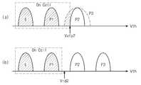
온 셀(on cell)의 수에 따른 공통 소스 라인 전압(Vcsl)의 변화를 살펴보기 위해, 다음과 같은 두 가지 가정을 한다. 첫째로, 선택 워드 라인(WL0)에 연결되어 있는 메모리 셀들은 각각 E, P1, P2, P3 상태로 프로그램된다고 가정한다. 여기에서, E 상태는 소거 상태를 의미하고, P3 상태에 있는 메모리 셀은 가장 높은 문턱 전압을 갖는다. P1과 P2 상태에 있는 메모리 셀은 E 상태와 P3 상태의 중간 레벨에 해당하는 문턱 전압을 갖는다. 둘째로, 선택 워드 라인(WL0)에 연결되어 있는 메모리 셀들이 온 셀일 때, 각각의 셀 스트링을 통해 흐르는 전류는 I0, I1, I2, I3라고 가정한다.To examine the variation of the common source line voltage (Vcsl) according to the number of on-cells, the following two assumptions are made. First, it is assumed that the memory cells connected to the selected word line WL0 are programmed to E, P1, P2, and P3 states, respectively. Here, the E state means an erase state, and the memory cell in the P3 state has the highest threshold voltage. The memory cell in the P1 and P2 states has a threshold voltage corresponding to the intermediate level between the E state and the P3 state. Second, when the memory cells connected to the selected word line WL0 are on-cells, it is assumed that the currents flowing through the respective cell strings are I0, I1, I2, I3.
이러한 가정에 따르면, 온 셀의 수의 따라 공통 소스 라인 전압(Vcsl)은 달라진다. 예를 들어, E 상태에 있는 메모리 셀만 온 셀이고 나머지 메모리 셀이 오프 셀이면, 공통 소스 라인 전압(Vcsl)은 I0*Rc가 된다. E와 P1 상태에 있는 메모리 셀이 온 셀이면, 공통 소스 라인 전압(Vcsl)은 (I0+I1)*Rc가 된다. 마찬가지로, E, P1, P2 상태에 있는 메모리 셀이 온 셀이면, 공통 소스 라인 전압(Vcsl)은 (I0+I1+I2)*Rc가 된다. 이는 프로그램 검증 동작과 읽기 동작 시에, 온 셀의 수가 달라지면 공통 소스 라인 전압(Vcsl)도 달라질 수 있음을 의미한다.According to this assumption, the common source line voltage Vcsl varies depending on the number of on-cells. For example, if only the memory cell in the E state is on-cell and the remaining memory cells are off-cell, the common source line voltage Vcsl becomes I0 * Rc. If the memory cells in the E and P1 states are on cells, the common source line voltage Vcsl is (I0 + I1) * Rc. Similarly, when the memory cells in the states E, P1 and P2 are on cells, the common source line voltage Vcsl is (I0 + I1 + I2) * Rc. This means that the common source line voltage (Vcsl) can also be changed when the number of on-cells is changed in the program verify operation and the read operation.
도 3은 도 2에 도시된 메모리 셀의 문턱 전압 분포를 보여주는 다이어그램이다. 도 3을 참조하면, 메모리 셀은 네 개의 상태(E, P1, P2, P3) 중에서 어느 하나를 갖는다.FIG. 3 is a diagram showing a threshold voltage distribution of the memory cell shown in FIG. 2. FIG. Referring to FIG. 3, the memory cell has one of four states (E, P1, P2, P3).
읽기 동작 시에 선택 워드 라인(WL0)으로 선택 읽기 전압(Vrd1, Vrd2, Vrd3)이 제공되고, 비선택 워드 라인(WL1~WL31)으로 비선택 읽기 전압(Vread)이 제공된 다. 제 1 선택 읽기 전압(Vrd1)은 소거 상태(E)와 제 1 프로그램 상태(P1) 사이의 전압 레벨을 갖고, 제 2 선택 읽기 전압(Vrd2)은 제 1 및 제 2 프로그램 상태(P1, P2) 사이의 전압 레벨을 갖고, 제 3 선택 읽기 전압(Vrd3)은 제 2 및 제 3 프로그램 상태(P2, P3) 사이의 전압 레벨을 갖는다.Selected read voltages Vrd1, Vrd2 and Vrd3 are provided to the selected word line WL0 and unselected read voltages Vread are provided to the unselected word lines WL1 to WL31 in the read operation. The first selected read voltage Vrd1 has a voltage level between the erased state E and the first programmed state P1 and the second selected read voltage Vrd2 has a voltage level between the first and second programmed states P1 and P2. And the third selected read voltage Vrd3 has a voltage level between the second and third programmed states P2 and P3.
제 1 선택 읽기 전압(Vrd1)을 인가할 때, 소거 상태(E)를 갖는 메모리 셀은 온 셀(on cell)이 되고 제 1 내지 제 3 프로그램 상태(P1, P2, P3)를 갖는 메모리 셀은 오프 셀(off cell)이 된다. 제 2 선택 읽기 전압(Vrd2)을 인가할 때, 소거 상태(E) 및 제 1 프로그램 상태(P1)를 갖는 메모리 셀은 온 셀(on cell)이 되고 제 2 및 제 3 프로그램 상태(P2, P3)를 갖는 메모리 셀은 오프 셀(off cell)이 된다. 제 3 선택 읽기 전압(Vrd3)을 인가할 때, 소거 상태(E), 제 1 및 제 2 프로그램 상태(P1, P2)를 갖는 메모리 셀은 온 셀(on cell)이 되고 제 3 프로그램 상태(P3)를 갖는 메모리 셀은 오프 셀(off cell)이 된다.The memory cell having the erase state E becomes on cell and the memory cell having the first to third program states P1, P2, and P3 is turned on when the first selected read voltage Vrd1 is applied Off cell. The memory cell having the erase state E and the first program state P1 becomes the on cell and the second and third program states P2 and P3 ) Is an off cell. The memory cell having the erase state E and the first and second programmed states P1 and P2 becomes on cell and the third programmed state P3 ) Is an off cell.
한편, 프로그램 검증 동작 시에 선택 워드 라인으로 프로그램 검증 전압(Vvfy1, Vvfy2, Vvfy3)이 제공된다. 제 1 프로그램 검증 전압(Vvfy1)은 메모리 셀을 제 1 프로그램 상태(P1)로 프로그램하기 위한 전압이고, 제 2 프로그램 검증 전압(Vvfy2)은 제 2 프로그램 상태(P2)로 프로그램하기 위한 전압이고, 제 3 프로그램 검증 전압(Vvfy3)은 제 3 프로그램 상태(P3)로 프로그램하기 위한 전압이다.On the other hand, the program verify voltages Vvfy1, Vvfy2, and Vvfy3 are supplied to the selected word line during the program verify operation. The first program verify voltage Vvfy1 is a voltage for programming the memory cell into the first program state P1 and the second program verify voltage Vvfy2 is a voltage for programming the second program state P2, 3 program verify voltage Vvfy3 is a voltage for programming into the third program state P3.
도 4 내지 도 6은 선택 워드 라인에 프로그램 검증 전압과 읽기 전압이 인가될 때 온 셀의 수를 보여주기 위한 다이어그램이다. 도 4 내지 도 6은 프로그램 검증 동작 시와 읽기 동작 시에 온 셀의 수가 달라질 수 있음을 보여준다. 도 2에서 설명한 바와 같이, 선택 워드 라인에 연결되어 있는 메모리 셀들의 온 셀의 수가 달라지면, 공통 소스 라인 전압(Vcsl)도 달라질 수 있다.4 to 6 are diagrams for illustrating the number of on-cells when a program verify voltage and a read voltage are applied to a selected word line. FIGS. 4 to 6 show that the number of on-cells can be varied during the program verify operation and the read operation. As described with reference to FIG. 2, if the number of on-cells of the memory cells connected to the selected word line is different, the common source line voltage Vcsl may also vary.
도 4는 선택 메모리 셀을 제 1 프로그램 상태(P1)로 프로그램하기 위한 프로그램 검증 동작과, 제 1 프로그램 상태(P1)에 있는 선택 메모리 셀을 읽기 위한 읽기 동작 시의 문턱 전압 분포를 각각 보여주는 다이어그램이다.4 is a diagram showing a program verify operation for programming the selected memory cell into the first program state P1 and a threshold voltage distribution in the read operation for reading the selected memory cell in the first program state P1 .
도 4(a)는 제 1 프로그램 검증 전압(Vvfy1)이 인가되는 경우에 온 셀(on cell)의 분포를 보여준다. 도 4(a)를 참조하면, 제 1 프로그램 검증 전압(Vvfy1) 인가 시에 온 셀로 되는 경우는 빗금 친 부분이다. 즉, 소거 상태(E)에 있는 메모리 셀과, 제 2 또는 제 3 프로그램 상태(P2 or P3)로 프로그램될 셀 중에서 문턱 전압이 아직 제 1 프로그램 검증 전압(Vvfy1)에 도달하지 못한 셀이 온 셀로 될 수 있다.4 (a) shows the distribution of on-cells when the first program verify voltage Vvfy1 is applied. Referring to FIG. 4 (a), when the first program verify voltage (Vvfy1) is applied to the on-cell, it is a hatched portion. That is, a cell in which the threshold voltage has not yet reached the first program verify voltage (Vvfy1) among the memory cells in the erase state E and the cells to be programmed in the second or third program state (P2 or P3) .
도 4(b)는 제 1 읽기 전압(Vrd1)이 인가되는 경우에 온 셀(on cell)의 분포를 보여준다. 도 4(b)를 참조하면, 제 1 읽기 전압(Vrd1) 인가 시에 온 셀로 되는 경우는 빗금 친 부분이다. 즉, 소거 상태(E)에 있는 메모리 셀만이 온 셀이다. 읽기 동작은 프로그램 검증 동작과는 달리, 모든 프로그램 동작이 종료된 다음에 수행되기 때문에, 제 2 또는 제 3 프로그램 상태(P2 or P3)로 프로그램될 셀들은 이미 제 2 또는 제 3 프로그램 상태에 도달해 있다. 따라서 제 1 읽기 전압(Vrd1) 인가 시에 온 셀로 되는 것은 소거 상태(E)에 있는 메모리 셀 뿐이다.FIG. 4 (b) shows the distribution of on-cells when the first read voltage Vrd1 is applied. Referring to FIG. 4 (b), when the first read voltage Vrd1 is applied, the cell is shaded. That is, only the memory cells in the erase state E are on-cells. Since the read operation is performed after all the program operations are completed, unlike the program verify operation, the cells to be programmed in the second or third program state (P2 or P3) have already reached the second or third program state have. Therefore, only the memory cell in the erase state E becomes the on-cell when the first read voltage Vrd1 is applied.
도 4(a)와 도 4(b)를 비교해 보면, 제 1 프로그램 상태(P1)를 읽기 위한 동작임에도 불구하고, 프로그램 검증 동작 시와 읽기 동작 시에 온 셀의 수가 달라짐 을 알 수 있다. 즉, 프로그램 검증 동작 시에 온 셀의 수가 읽기 동작 시의 온 셀의 수보다 더 많다. 온 셀 수의 차이는 제 2 또는 제 3 프로그램 상태(P2 or P3)로 프로그램될 셀 중에서 문턱 전압이 아직 제 1 프로그램 검증 전압(Vvfy1)에 도달하지 못한 메모리 셀 때문이다.Comparing FIG. 4A and FIG. 4B, it can be seen that the number of on-cells differs between the program verify operation and the read operation, despite the operation for reading the first program state P1. That is, the number of on-cells in the program verify operation is larger than the number of on-cells in the read operation. The difference in the on-cell number is due to the memory cell whose threshold voltage has not yet reached the first program verify voltage (Vvfy1) among the cells to be programmed in the second or third program state (P2 or P3).
도 5는 선택 메모리 셀을 제 2 프로그램 상태(P2)로 프로그램하기 위한 프로그램 검증 동작과, 제 2 프로그램 상태(P2)에 있는 선택 메모리 셀을 읽기 위한 읽기 동작 시의 문턱 전압 분포를 각각 보여주는 다이어그램이다.5 is a diagram showing a program verify operation for programming the selected memory cell to the second programmed state P2 and a threshold voltage distribution for the read operation for reading the selected memory cell in the second programmed state P2 .
도 5(a)는 제 2 프로그램 검증 전압(Vvfy2)이 인가되는 경우에 온 셀(on cell)의 분포를 보여준다. 제 2 프로그램 검증 전압(Vvfy2) 인가 시에 온 셀은 소거 상태(E) 및 제 1 프로그램 상태(P1)에 있는 메모리 셀과, 제 3 프로그램 상태(P3)로 프로그램될 셀 중에서 문턱 전압이 아직 제 2 프로그램 검증 전압(Vvfy2)에 도달하지 못한 메모리 셀이다.5 (a) shows the distribution of on-cells when the second program verify voltage Vvfy2 is applied. When the second program verify voltage Vvfy2 is applied, the on-cell is in the erased state E and the memory cell in the first programmed state P1 and the cell to be programmed in the third programmed state P3, 2 program verify voltage (Vvfy2).
도 5(b)는 제 2 읽기 전압(Vrd2)이 인가되는 경우에 온 셀(on cell)의 분포를 보여준다. 도 5(b)를 참조하면, 제 2 읽기 전압(Vrd2) 인가 시에 온 셀은 소거 상태(E) 및 제 1 프로그램 상태(P1)에 있는 메모리 셀이다. 이는 제 3 프로그램 상태(P3)로 프로그램될 셀들은 이미 제 3 프로그램 상태(P3)에 도달해 있기 때문이다.5 (b) shows the distribution of on-cells when the second read voltage Vrd2 is applied. Referring to FIG. 5 (b), the on-cell is a memory cell in the erased state E and the first programmed state P1 when the second read voltage Vrd2 is applied. This is because the cells to be programmed in the third program state P3 have already reached the third program state P3.
도 5(a)와 도 5(b)를 비교해 보면, 제 2 프로그램 상태(P2)를 읽기 위한 동작임에도 불구하고, 프로그램 검증 동작 시와 읽기 동작 시에 온 셀의 수가 달라질 수 있다. 즉, 프로그램 검증 동작 시에 온 셀의 수가 읽기 동작 시의 온 셀의 수보 다 더 많다. 온 셀 수의 차이는 제 3 프로그램 상태(P3)로 프로그램될 셀 중에서 문턱 전압이 아직 제 2 프로그램 검증 전압(Vvfy2)에 도달하지 못한 메모리 셀 때문이다.5A and 5B, although the operation for reading the second program state P2 is performed, the number of on-cells in the program verify operation and the read operation can be varied. That is, the number of on-cells in the program verify operation is more than the number of on-cells in the read operation. The difference in the on-cell number is due to the memory cell whose threshold voltage has not yet reached the second program verify voltage Vvfy2 among the cells to be programmed in the third program state P3.
도 6은 선택 메모리 셀을 제 3 프로그램 상태(P3)로 프로그램하기 위한 프로그램 검증 동작과, 제 3 프로그램 상태(P3)에 있는 선택 메모리 셀을 읽기 위한 읽기 동작 시의 문턱 전압 분포를 각각 보여주는 다이어그램이다.6 is a diagram showing a program verify operation for programming the selected memory cell into the third program state P3 and a threshold voltage distribution in the read operation for reading the selected memory cell in the third program state P3 .
도 6(a)는 제 3 프로그램 검증 전압(Vvfy3)이 인가되는 경우에 온 셀(on cell)의 분포를 보여준다. 제 3 프로그램 검증 전압(Vvfy3) 인가 시에 온 셀은 소거 상태(E), 제 1 및 제 2 프로그램 상태(P1, P2)에 있는 메모리 셀이다. 도 6(b)는 제 3 읽기 전압(Vrd3)이 인가되는 경우에 온 셀(on cell)의 분포를 보여준다. 도 6(b)를 참조하면, 제 3 읽기 전압(Vrd3) 인가 시에 온 셀은 소거 상태(E), 제 1 및 제 2 프로그램 상태(P1, P2)에 있는 메모리 셀이다.6 (a) shows the distribution of on-cells when the third program verify voltage Vvfy3 is applied. The on-cell at the time of applying the third program verify voltage Vvfy3 is a memory cell in the erase state E, the first and second program states P1 and P2. 6 (b) shows the distribution of on-cells when the third read voltage Vrd3 is applied. Referring to FIG. 6 (b), the on-cell at the time of applying the third read voltage Vrd3 is a memory cell in the erase state E and the first and second program states P1 and P2.
도 6(a)와 도 6(b)를 비교해 보면, 제 3 프로그램 상태(P3)를 읽기 위한 동작 시에는 프로그램 검증 동작과 읽기 동작에서의 온 셀의 수가 같아진다. 이는 제 3 프로그램 상태(P3)로 프로그램될 셀이 모두 제 3 프로그램 검증 전압(Vvfy3)에 도달하기 때문이다.6 (a) and 6 (b), in the operation for reading the third program state P3, the number of on-cells in the program verify operation and the read operation becomes equal. This is because all the cells to be programmed in the third program state P3 reach the third program verify voltage Vvfy3.
도 4 내지 도 6을 참조하면, P1 또는 P2 상태로 프로그램하기 위한 프로그램 검증 동작과, P1 또는 P2 상태를 읽기 위한 읽기 동작 시에 온 셀의 수가 달라질 수도 있다. 동일 상태에 대해 프로그램 검증 동작과 읽기 동작 시에 온 셀의 수가 달라지면, 앞에서 설명한 바와 같이 공통 소스 라인 전압(Vcsl)이 달라진다. 이와 같이 공통 소스 라인(CSL)에 존재하는 노이즈(noise)로 인해, 메모리 셀의 문턱 전압 분포 폭이 넓어질 수 있다. 이것은 도 7에서 상세하게 설명된다.Referring to FIGS. 4 to 6, the number of on-cells may be varied during a program verify operation for programming into the P1 or P2 state and a read operation for reading the P1 or P2 state. When the number of on-cells differs between the program verify operation and the read operation with respect to the same state, the common source line voltage Vcsl varies as described above. As described above, due to the noise existing in the common source line CSL, the threshold voltage distribution width of the memory cell can be widened. This is explained in detail in Fig.
도 7은 공통 소스 라인 전압에 존재하는 노이즈로 인해 메모리 셀의 문턱 전압 분포 폭이 넓어지는 것을 보여주는 다이어그램이다. 도 7에서는 제 1 프로그램 상태(P1)만을 보여주고 있으나, 제 2 프로그램 상태(P2)에서도 문턱 전압 분포의 변화는 동일하게 나타난다.7 is a diagram showing that the threshold voltage distribution width of a memory cell is widened due to noise existing in a common source line voltage. Although only the first program state P1 is shown in Fig. 7, the change in the threshold voltage distribution is the same even in the second program state P2.
위에서 설명한 바와 같이, 온 셀의 수는 프로그램 검증 동작 시가 읽기 동작 시보다 많아질 수 있다. 프로그램 검증 동작 시에 온 셀의 수가 많아지면, 공통 소스 라인에 흐르는 전류량이 증가한다. 공통 소스 라인에 흐르는 전류량이 증가하면, 기생 저항 등의 영향으로 인해 공통 소스 라인 전압(Vcsl)이 높아진다. 공통 소스 라인 전압(Vcsl)이 높아지면, 도 7의 점선(P1')에서 보는 바와 같이 메모리 셀들의 문턱 전압 분포가 넓어지게 된다.As described above, the number of on-cells can be larger during the program verify operation than during the read operation. When the number of on-cells increases in the program verify operation, the amount of current flowing in the common source line increases. When the amount of current flowing in the common source line increases, the common source line voltage Vcsl increases due to the influence of parasitic resistance or the like. As the common source line voltage Vcsl increases, the threshold voltage distribution of the memory cells becomes wider as shown by the dotted line P1 'in FIG.
도 8은 본 발명에 따른 플래시 메모리 장치의 프로그램 방법을 보여주는 그래프이다. 도 8에서, 가로축은 프로그램 루프(program loop)에 따른 프로그램 진행 시간을 나타내고, 세로축은 워드 라인으로 제공되는 프로그램 전압(Vpgm) 및 프로그램 검증 전압(Vvfy)을 나타낸다.8 is a graph showing a programming method of a flash memory device according to the present invention. 8, the horizontal axis represents the program progress time according to a program loop, and the vertical axis represents the program voltage Vpgm and the program verify voltage Vvfy provided on the word line.
일반적으로 플래시 메모리 장치는 프로그램 동작 시에 메모리 셀의 문턱 전압(threshold voltage) 분포의 폭을 좁게 만들기 위해서 "증가형 스텝 펄스 프로그램" (Incremental Step Pulse Program; ISPP) 방법을 사용한다. 증가형 스텝 펄스 프로그램 방법에 의하면, 선택 워드 라인으로 인가되는 프로그램 전압은 프로그램 루프(program loop)에 따라 단계적으로 증가한다.Generally, a flash memory device uses an " Incremental Step Pulse Program "(ISPP) method to narrow the width of the threshold voltage distribution of memory cells during program operation. According to the incremental step pulse programming method, the program voltage applied to the selected word line increases stepwise in accordance with the program loop.
플래시 메모리 장치의 프로그램 동작은 각각의 프로그램 루프(program loop)에서, 프로그램 실행(program execution) 및 프로그램 검증(progam verify)을 수행한다. 프로그램 실행 동작에서는 선택 워드 라인으로 프로그램 전압(Vpgm)이 제공되고, 프로그램 검증 동작에서는 프로그램 검증 전압(Vvfy)이 제공된다.The program operation of the flash memory device performs program execution and program verification in each program loop. In the program execution operation, the program voltage Vpgm is provided as the selected word line, and the program verification voltage Vvfy is provided in the program verification operation.
플래시 메모리 장치는 페이지 단위로 프로그램 동작을 수행한다. 종래의 플래시 메모리 장치는 각각의 프로그램 루프마다, 하나의 페이지에 대해서 프로그램 실행 또는 프로그램 검증 동작이 수행된다. 반면에, 본 발명에 따른 플래시 메모리 장치는 하나의 페이지를 복수의 영역(region)으로 분할(split)한다. 본 발명은 하나의 페이지에 대해 프로그램 실행이 동시에 수행되고, 각각의 분할 영역(split region)에 대해 프로그램 검증 동작이 순차적으로 수행된다. 본 발명에 의하면, 프로그램 검증 동작이 분할 영역에 따라 순차적으로 수행되기 때문에, 공통 소스 라인의 노이즈를 줄일 수 있다.The flash memory device performs a program operation on a page basis. In the conventional flash memory device, program execution or program verification operation is performed for one page for each program loop. On the other hand, the flash memory device according to the present invention divides one page into a plurality of regions. In the present invention, program execution is performed simultaneously for one page, and a program verification operation is sequentially performed for each split region. According to the present invention, since the program verify operation is sequentially performed in accordance with the divided regions, the noise of the common source line can be reduced.
도 8에 도시된 프로그램 동작은 4 스텝 검증 루프, 2 스텝 검증 루프, 그리고 1 스텝 검증 루프로 구성된다. 프로그램 루프 초반(예를 들면, PGM LOOP A)에는 4 스텝 검증 루프가 수행되고, 프로그램 루프 중반(예를 들면, PGM LOOP B)에는 2 스텝 검증 루프가 수행되고, 프로그램 루프 후반(예를 들면, PGM LOOP C)에는 1 스텝 검증 루프가 수행된다.The program operation shown in Fig. 8 consists of a 4-step verification loop, a 2-step verification loop, and a 1-step verification loop. A four step verification loop is performed at the beginning of the program loop (e.g., PGM LOOP A), a two step verification loop is performed at the middle of the program loop (e.g., PGM LOOP B) PGM LOOP C) performs a one step verification loop.
4 스텝 검증 루프에서는 하나의 페이지가 4개의 영역으로 분할된다. 하나의 페이지에 대해 프로그램 실행 동작이 동시에 수행되고, 각각의 분할 영역에 대해 프로그램 검증 동작이 순차적으로 수행된다. 2 스텝 검증 루프에서는 하나의 페이지가 2개의 영역으로 분할되고, 각각의 분할 영역에 대해 프로그램 검증 동작이 순차적으로 수행된다. 1 스텝 검증 루프에서는 영역 분할(region split) 없이 하나의 페이지에 프로그램 실행 또는 프로그램 검증 동작이 동시에 수행된다.In a four-step verification loop, one page is divided into four regions. A program execution operation is simultaneously performed for one page, and a program verification operation is sequentially performed for each of the divided areas. In a two-step verification loop, one page is divided into two areas, and a program verification operation is sequentially performed for each of the divided areas. In a one-step verification loop, program execution or program verification operations are performed simultaneously on one page without region splitting (region split).
도 9는 본 발명의 프로그램 방법에 따른 영역 분할 방식의 제 1 실시 예를 보여주는 다이어그램이다. 도 9에서, 플래시 메모리 장치는 하나의 페이지가 16개의 메모리 셀(MC1~16)로 구성된다고 가정한다. 각각의 메모리 셀(MC1~MC16)은 해당하는 비트 라인(BL1~BL16)과 공통 소스 라인(CSL) 사이에 연결되어 있다.FIG. 9 is a diagram illustrating a first embodiment of a region partitioning method according to the program method of the present invention. In Fig. 9, it is assumed that one page is composed of sixteen memory cells MC1 to MC16 in the flash memory device. Each of the memory cells MC1 to MC16 is connected between the corresponding bit line BL1 to BL16 and the common source line CSL.
도 9(a)는 4 스텝 검증 방식을 보여준다. 도 9(a)를 참조하면, 하나의 페이지는 4개의 영역으로 분할된다. 제 1 영역은 제 1 내지 제 4 메모리 셀(MC1~MC4)에 해당하고, 제 2 영역은 제 5 내지 제 8 메모리 셀(MC5~MC8)에 해당하고, 제 3 영역은 제 9 내지 제 12 메모리 셀(MC9~MC12)에 해당하고, 제 4 영역은 제 13 내지 제 16 메모리 셀(MC13~MC16)에 해당한다.Figure 9 (a) shows a four-step verification scheme. Referring to Fig. 9 (a), one page is divided into four regions. The first area corresponds to the first to fourth memory cells MC1 to MC4, the second area corresponds to the fifth to eighth memory cells MC5 to MC8, the third area corresponds to the ninth to twelfth memory cells MC5 to MC8, Cells MC9 to MC12, and the fourth region corresponds to the thirteenth to sixteenth memory cells MC13 to MC16.
다시 도 8을 참조하면, 프로그램 루프 A에서, 프로그램 실행 동작은 하나의 페이지에 대해 동시에 수행된다. 즉, 모든 메모리 셀(MC1~MC16)에 프로그램 실행 동작이 동시에 수행된다. 그러나 프로그램 검증 동작은 제 1 영역에서 제 4 영역까지 4 번에 걸쳐서 순차적으로 수행된다. 즉, 제 1 영역에 해당하는 메모리 셀(MC1~MC4)에 대해 1차적으로 프로그램 검증 동작이 수행되고, 다음으로 제 2 내지 제 4 영역에 해당하는 메모리 셀에 대해 순차적으로 프로그램 검증 동작이 수행된다.Referring again to Fig. 8, in the program loop A, the program execution operation is performed simultaneously for one page. That is, program execution operations are simultaneously performed on all the memory cells MC1 to MC16. However, the program verification operation is performed sequentially from the first area to the fourth area four times. That is, a program verify operation is primarily performed on the memory cells MC1 to MC4 corresponding to the first region, and a program verify operation is sequentially performed on the memory cells corresponding to the second to fourth regions .
도 9(b)는 2 스텝 검증 방식을 보여준다. 도 9(b)를 참조하면, 하나의 페이지는 2개의 영역으로 분할된다. 제 1 영역은 제 1 내지 제 8 메모리 셀(MC1~MC8)에 해당하고, 제 2 영역은 제 9 내지 제 16 메모리 셀(MC9~MC16)에 해당한다. 도 8에 도시된 프로그램 루프 B에서, 프로그램 실행 동작은 하나의 페이지에 대해 동시에 수행된다. 그러나 프로그램 검증 동작은 제 1 영역에서 제 2 영역까지 2 번에 걸쳐서 순차적으로 수행된다.9 (b) shows a two-step verification method. Referring to Fig. 9 (b), one page is divided into two regions. The first area corresponds to the first to eighth memory cells MC1 to MC8, and the second area corresponds to the ninth to sixteenth memory cells MC9 to MC16. In the program loop B shown in Fig. 8, the program execution operation is performed simultaneously for one page. However, the program verification operation is sequentially performed twice from the first area to the second area.
도 9(c)는 1 스텝 검증 방식을 보여준다. 도 9(c)를 참조하면, 플래시 메모리 장치는 영역 분할 없이 하나의 페이지에 대해 프로그램 실행 또는 프로그램 검증 동작을 수행한다.Fig. 9 (c) shows a one-step verification method. Referring to FIG. 9 (c), the flash memory device performs a program execution or program verification operation for one page without area division.
도 9에 도시된 영역 분할 방식은 이웃하는 메모리 셀을 하나의 영역으로 분할한다. 예를 들면, 도 9에서 보는 바와 같이 하나의 페이지를 4개의 영역으로 분할하는 경우에, 제 1 내지 제 4 메모리 셀(MC1~MC4)은 하나의 영역에 속한다. 하나의 페이지를 4개의 영역으로 분할하는 경우에, 제 1 내지 제 4 메모리 셀(MC1~MC4)은 하나의 영역에 속한다.The area division scheme shown in FIG. 9 divides the neighboring memory cells into one area. For example, as shown in FIG. 9, when one page is divided into four regions, the first to fourth memory cells MC1 to MC4 belong to one region. In the case of dividing one page into four regions, the first to fourth memory cells MC1 to MC4 belong to one region.
도 10은 본 발명의 프로그램 방법에 따른 영역 분할 방식의 제 2 실시 예를 보여주는 다이어그램이다. 도 10에서, 플래시 메모리 장치는 하나의 페이지가 16개의 메모리 셀(MC1~16)로 구성된다고 가정한다. 각각의 메모리 셀(MC1~MC16)은 해당하는 비트 라인(BL1~BL16)과 공통 소스 라인(CSL) 사이에 연결되어 있다.FIG. 10 is a diagram showing a second embodiment of the area division method according to the programming method of the present invention. In Fig. 10, it is assumed that one page is composed of sixteen memory cells MC1 to MC16 in the flash memory device. Each of the memory cells MC1 to MC16 is connected between the corresponding bit line BL1 to BL16 and the common source line CSL.
도 10(a)은 4 스텝 검증 방식을 보여준다. 도 10(a)를 참조하면, 하나의 페이지는 4개의 영역으로 분할된다. 제 1 영역은 제 1, 5, 9, 13 메모리 셀(MC1, MC5, MC9, MC13)에 해당하고, 제 2 영역은 제 2, 6, 10, 14 메모리 셀(MC2, MC6, MC10, MC14)에 해당하고, 제 3 영역은 제 3, 7, 11, 15 메모리 셀(MC3, MC7, MC11, MC15)에 해당하고, 제 4 영역은 제 4, 8, 12, 16 메모리 셀(MC4, MC8, MC12, MC16)에 해당한다. 도 9(a)와 마찬가지로, 프로그램 검증 동작은 제 1 영역에서 제 4 영역까지 4 번에 걸쳐서 순차적으로 수행된다.10 (a) shows a four-step verification method. Referring to Fig. 10 (a), one page is divided into four regions. The first region corresponds to the first, fifth, ninth and thirteenth memory cells MC1, MC5, MC9 and MC13 and the second region corresponds to the second, sixth, tenth and fourteenth memory cells MC2, MC6, MC10 and MC14. And the fourth region corresponds to the fourth, eighth, twelfth, and sixteenth memory cells MC4, MC8, MC15, MC15, and the third region corresponds to the third, seventh, MC12, MC16). As in Fig. 9A, the program verify operation is sequentially performed four times from the first region to the fourth region.
도 10(b)는 2 스텝 검증 방식을 보여준다. 도 10(b)를 참조하면, 하나의 페이지는 2개의 영역으로 분할된다. 제 1 영역은 홀수 번째 메모리 셀(MCi; i=1, 3, 5, 7, 9, 11, 13, 15)에 해당하고, 제 2 영역은 짝수 번째 메모리 셀(MCj; j=2, 4, 6, 8, 10, 12, 14, 16)에 해당한다. 도 9(b)와 마찬가지로, 프로그램 검증 동작은 제 1 영역에서 제 2 영역까지 2 번에 걸쳐서 순차적으로 수행된다.10 (b) shows a two-step verification method. Referring to Fig. 10 (b), one page is divided into two regions. The first region corresponds to the odd-numbered memory cells MCi (i = 1, 3, 5, 7, 9, 11, 13, 15), the second region corresponds to the even- 6, 8, 10, 12, 14, 16). As in FIG. 9 (b), the program verify operation is sequentially performed twice from the first area to the second area.
도 10(c)는 1 스텝 검증 방식을 보여준다. 도 10(c)를 참조하면, 플래시 메모리 장치는 영역 분할 없이 하나의 페이지에 대해 프로그램 실행 또는 프로그램 검증 동작을 수행한다.10 (c) shows a one-step verification method. Referring to FIG. 10 (c), the flash memory device performs a program execution or program verification operation for one page without area division.
도 10에 도시된 영역 분할 방식은 이웃하지 않는 메모리 셀을 하나의 영역으로 분할한다. 예를 들면, 도 10에서 보는 바와 같이 하나의 페이지를 2개의 영역으로 분할하는 경우에, 홀수 번째 메모리 셀과 짝수 번째 메모리 셀은 서로 다른 영역에 속한다. 본 발명에 따른 플래시 메모리 장치의 영역 분할 방식은 도 9 및 도 10 도시된 방식 이외의 여러 가지 다른 형태로 구현될 수 있다.The area division scheme shown in FIG. 10 divides non-neighboring memory cells into one area. For example, as shown in FIG. 10, when one page is divided into two regions, odd-numbered memory cells and even-numbered memory cells belong to different regions. The area division method of the flash memory device according to the present invention can be implemented in various other forms other than the method shown in FIGS.
다시 도 8을 참조하면, 본 발명에 따른 플래시 메모리 장치는 프로그램 루프를 진행하면서 영역 분할 수를 가변한다. 프로그램 루프 초반(예를 들면, PGM LOOP A)에는 대부분의 메모리 셀이 온 셀이기 때문에, 공통 소스 라인(CSL)은 큰 노이즈(noise)를 갖는다. 본 발명은 공통 소스 라인(CSL)의 노이즈를 줄이기 위해서, 하나의 페이지를 복수의 영역으로 분할하고, 분할된 영역 단위로 프로그램 검증 동작을 수행한다. 프로그램 루프 초반의 4 스텝 검증 루프 단계에서는 하나의 페이지를 4개의 영역으로 분할하고, 4 번의 프로그램 검증 동작이 수행된다.Referring again to FIG. 8, the flash memory device according to the present invention varies the number of area divisions while performing a program loop. In the early part of the program loop (for example, PGM LOOP A), since most of the memory cells are on-cells, the common source line CSL has a large noise. In order to reduce the noise of the common source line (CSL), the present invention divides one page into a plurality of regions and performs a program verification operation in units of divided regions. In the 4 step verification loop phase in the beginning of the program loop, one page is divided into four regions and four program verification operations are performed.
프로그램 루프 중반(예를 들면, PGM LOOP B)에는 프로그램 완료된 셀이 증가하기 때문에, 프로그램 검증 동작 시에 온 셀의 수가 줄어든다. 따라서 프로그램 루프 중반에는 프로그램 루프 초기보다 영역 분할의 수를 줄여서, 프로그램 속도를 빠르게 할 수 있다. 프로그램 루프 중반의 2 스텝 검증 루프 단계에서는 하나의 페이지를 2개의 영역으로 분할하고, 2 번의 프로그램 검증 동작이 수행된다.In the middle of the program loop (for example, PGM LOOP B), since the number of programmed cells increases, the number of on-cells decreases in the program verify operation. Therefore, in the middle of the program loop, the program speed can be increased by reducing the number of area divisions more than at the beginning of the program loop. In the two step verification loop phase of the middle of the program loop, one page is divided into two regions and two program verification operations are performed.
프로그램 루프 후반(예를 들면, PGM LOOP C)에는 대부분의 메모리 셀이 프로그램 완료된다. 따라서 프로그램 루프 후반에는 영역 분할 없이 프로그램 검증 동작을 한 번에 수행함으로, 프로그램 속도를 빠르게 할 수 있다. 프로그램 루프 후반의 1 스텝 검증 루프 단계에서는 하나의 페이지를 영역 분할하지 않고, 1 번의 프로그램 검증 동작이 수행된다.In the latter part of the program loop (for example, PGM LOOP C), most of the memory cells are programmed. Therefore, in the latter part of the program loop, the program verification operation is performed at once without performing the area division, thereby making it possible to speed up the program. In the one step verification loop step of the latter half of the program loop, one program verification operation is performed without dividing one page into regions.
본 발명에 따른 플래시 메모리 장치는 도 8에 도시된 바와 같이, 프로그램 루프에 따라 영역 분할 수를 조절함으로, CSL 노이즈를 줄임과 동시에 프로그램 속도를 빠르게 할 수 있다. 프로그램 루프에 따라 영역 분할 수를 가변하는 방법은 도 11 내지 도 13에서 상세하게 설명된다. 영역 분할 수의 가변은 공통 소스 라인 전압(Vcsl)을 검출함으로 수행된다.As shown in FIG. 8, the flash memory device according to the present invention adjusts the number of area divisions according to a program loop, thereby reducing the CSL noise and speeding up the program. The method of varying the number of region divisions according to the program loop will be described in detail in Figs. 11 to 13. Fig. The variable of the number of divided regions is performed by detecting the common source line voltage Vcsl.
도 11은 각각의 프로그램 루프마다 공통 소스 라인 전압(Vcsl)을 검출함으로,영역 분할 수를 조절하는 방법을 보여주는 그래프이다. 도 11을 참조하면, 플래시 메모리 장치는 공통 소스 라인 전압(Vcsl)에 따라 4 스텝 검증 루프, 2 스텝 검증 루프, 그리고 1 스텝 검증 루프를 갖는다.11 is a graph showing a method of adjusting the number of region divisions by detecting the common source line voltage Vcsl for each program loop. Referring to FIG. 11, the flash memory device has a 4-step verification loop, a 2-step verification loop, and a 1-step verification loop according to the common source line voltage Vcsl.
도 11에 도시된 영역 분할 수를 조절하는 방법은 각각의 프로그램 루프마다 공통 소스 라인 전압(Vcsl)을 검출한다. 예를 들어, 이전 프로그램 루프(pervious progam loop)에서 4 스텝 검증 동작이 수행되었다고 가정하자. 현재 프로그램 루프(now program loop)에서 공통 소스 라인 전압(Vcsl)이 4 스텝 검증 루프 구간에 있으면 다음 프로그램 루프(next program loop)에서는 4 스텝 검증 동작이 수행되고, 2 스텝 검증 루프 구간에 있으면 다음 프로그램 루프에서는 2 스텝 검증 동작이 수행된다.The method of adjusting the number of region divisions shown in Fig. 11 detects the common source line voltage Vcsl for each program loop. For example, suppose that a four step verification operation was performed in a previous program loop (pervious progam loop). If the common source line voltage (Vcsl) in the current program loop (current program loop) is in the 4-step verification loop section, the 4-step verification operation is performed in the next program loop. In the loop, a two step verification operation is performed.
마찬가지로, 이전 프로그램 루프에서 2 스텝 검증 동작이 수행되었다고 가정하자. 현재 프로그램 루프에서 공통 소스 라인 전압(Vcsl)이 2 스텝 검증 루프 구간에 있으면 다음 프로그램 루프에서는 2 스텝 검증 동작이 수행되고, 1 스텝 검증 루프 구간에 있으면 다음 프로그램 루프에서는 1 스텝 검증 동작이 수행된다.Likewise, assume that a two step verification operation has been performed in the previous program loop. If the common source line voltage (Vcsl) in the current program loop is in the 2-step verification loop section, a 2-step verification operation is performed in the next program loop.
도 11을 참조하면, 4 스텝 검증 루프의 마지막 프로그램 루프에서 2 스텝 검증 루프에 해당하는 공통 소스 라인 전압(Vcsl)이 검출되면, 다음 프로그램 루프에서는 2 스텝 검증 동작이 수행된다. 마찬가지로 2 스텝 검증 루프의 마지막 프로그램 루프에서 1 스텝 검증 루프에 해당하는 공통 소스 라인 전압(Vcsl)이 검출되면, 다음 프로그램 루프에서는 1 스텝 검증 동작이 수행된다.Referring to FIG. 11, when the common source line voltage Vcsl corresponding to the two-step verification loop in the last program loop of the four-step verification loop is detected, a two-step verification operation is performed in the next program loop. Similarly, when the common source line voltage Vcsl corresponding to the one-step verification loop in the last program loop of the two-step verification loop is detected, a one-step verification operation is performed in the next program loop.
도 11에 도시된 영역 분할 수를 조절하는 방법은 별도로 공통 소스 라인 전압(Vcsl)을 검출하는 구간을 두지 않는다. 현재 프로그램 루프가 진행되는 동안에 공통 소스 라인 전압(Vcsl)이 검출되고, 다음 프로그램 루프의 영역 분할 수가 결정된다.The method of adjusting the number of divided regions shown in Fig. 11 does not have a section for detecting the common source line voltage Vcsl separately. During the current program loop, the common source line voltage Vcsl is detected, and the number of region divisions of the next program loop is determined.
도 12는 더미 프리차지 구간에서 공통 소스 라인 전압(Vcsl)을 검출함으로, 영역 분할 수를 조절하는 방법을 보여주는 그래프이다. 더미 프리차지 동작(dummy precharge operation)은 프로그램 루프 이전 또는 이후에 수행될 수 있다. 더미 프리차지 구간에서, 모든 비트 라인을 프리차지 한 상태에서 공통 소스 라인 전압(Vcsl)을 검출한다.12 is a graph showing a method of adjusting the number of region divisions by detecting the common source line voltage Vcsl in the dummy precharge period. The dummy precharge operation may be performed before or after the program loop. In the dummy precharge period, the common source line voltage Vcsl is detected in a state in which all the bit lines are precharged.
도 12에 도시된 영역 분할 가변 방법은 모든 비트 라인을 프리차지 하기 때문에, 공통 소스 라인 전압(Vcsl)의 검출 레벨을 높일 수 있다는 장점을 갖는다. 그러나 도 12에 도시된 영역 분할 가변 방법은 다수의 더미 프리차지 구간으로 인하여 프로그램 시간이 증가하는 단점을 갖는다.The region dividing variable method shown in Fig. 12 has an advantage that the detection level of the common source line voltage Vcsl can be raised because all the bit lines are precharged. However, the area division variable method shown in FIG. 12 has a disadvantage in that the program time increases due to a plurality of dummy precharge periods.
도 13은 프로그램 초기에 공통 소스 라인 전압(Vcsl)을 검출함으로, 영역 분할 수를 조절하는 방법을 보여주는 그래프이다. 더미 프리차지 동작(dummy precharge operation)은 프로그램 초기에 한 번 수행된다. 더미 프리차지 구간에서 플래시 메모리 장치는 모든 비트 라인을 프리차지 하고, 공통 소스 라인 전압(Vcsl)을 검출한다. 플래시 메모리 장치는 검출된 공통 소스 라인 전압(Vcsl)에 따라, 이후의 프로그램 루프의 영역 분할 수를 결정한다. 프로그램 루프의 영역 분할 수는 공통 소스 라인 전압(Vcsl)을 검출한 다음에, 미리 정의된 데이터에 따라 영역 분할 수를 결정할 수 있다.13 is a graph showing a method of adjusting the number of region divisions by detecting the common source line voltage Vcsl at the beginning of a program. The dummy precharge operation is performed once at the beginning of the program. In the dummy precharge period, the flash memory device precharges all the bit lines and detects the common source line voltage Vcsl. The flash memory device determines the number of area divisions of the subsequent program loop in accordance with the detected common source line voltage Vcsl. The number of region divisions of the program loop can be determined based on the predefined data after detecting the common source line voltage Vcsl.
도 11 내지 도 13에 도시된 영역 분할 수를 조절하는 방법은 공통 소스 라인 전압(Vcsl)을 검출하고, 그 결과에 따라 이후 프로그램 루프에서의 영역 분할 수를 결정한다. 그러나 본 발명에 따른 플래시 메모리 장치는 공통 소스 라인 전압(Vcsl)을 검출하지 않고, 각각의 프로그램 루프에서 영역 분할 수를 정할 수 있다.11 to 13 detects the common source line voltage Vcsl and determines the number of area divisions in the program loop thereafter in accordance with the result. However, the flash memory device according to the present invention can determine the number of area divisions in each program loop without detecting the common source line voltage Vcsl.
예를 들어, 프로그램 루프 수가 10회라고 가정하자. 제 1 내지 제 4 프로그램 루프에서는 4 스텝 검증 동작이 수행되도록 정하고, 제 5 내지 제 7 프로그램 루프에서는 2 스텝 검증 동작이 수행되도록 정하고, 제 8 내지 제 10 프로그램 루프에서는 1 스텝 검증 동작이 수행되도록 정할 수 있다. 또한, 본 발명에 따른 플래시 메모리 장치는 프로그램 데이터의 수를 카운트함으로 영역 분할 수를 조절할 수 있다.For example, suppose the number of program loops is ten. In the first to fourth program loops, the four-step verification operation is performed. In the fifth to seventh program loops, the two-step verification operation is performed. In the eighth to tenth program loops, . In addition, the flash memory device according to the present invention can adjust the number of area divisions by counting the number of program data.
도 14 내지 도 16은 프로그램 데이터의 수에 따라 영역 분할 수를 조절하는 방법을 보여준다. 이하에서, 플래시 메모리 장치(도 1 참조, 100)는 메모리 셀 어레이(도 1 참조, 110) 및 데이터 입출력 제어 회로(도 1 참조, 120)를 포함하고, 각각의 메모리 셀은 4개의 프로그램 상태(E, P1, P2, P3)를 갖는다고 가정한다.FIGS. 14 to 16 show a method of adjusting the number of area divisions according to the number of program data. Hereinafter, a flash memory device (see FIG. 1) 100 includes a memory cell array (see FIG. 1) 110 and a data input / output control circuit (see FIG. 1) 120, E, P1, P2, P3).
도 14는 각각의 프로그램 상태에 해당하는 프로그램 데이터의 수를 예시적으로 보여주는 그래프이다. 도 14를 참조하면, 가로축은 메모리 셀의 프로그램 상태(program state)를 나타내고, 세로축은 프로그램 데이터의 수를 나타낸다. 도 14에서, P1 프로그램 데이터의 수는 1 스텝 검증 구간에 해당한다. P2 프로그램 데이 터의 수는 4 스텝 검증 구간에 해당한다. 그리고 P3 프로그램 데이터의 수는 2 스텝 검증 구간에 해당한다. 따라서 프로그램 초반에 P1 프로그램 동작은 1 스텝 검증 동작을 수행하고, P2 프로그램 동작은 4 스텝 검증 동작을 수행하고, P3 프로그램 동작은 2 스텝 검증 동작을 수행한다.14 is a graph showing an example of the number of program data corresponding to each program state. Referring to FIG. 14, the horizontal axis represents a program state of a memory cell, and the vertical axis represents the number of program data. In Fig. 14, the number of P1 program data corresponds to one step verification period. The number of P2 program data corresponds to the 4 step verification period. And the number of P3 program data corresponds to a two-step verification period. Therefore, at the beginning of the program, the P1 program operation performs one step verification operation, the P2 program operation performs four step verification operation, and the P3 program operation performs two step verification operation.
도 15는 각각의 프로그램 상태에 해당하는 프로그램 루프를 보여주는 다이어그램이다. 도 15(a)는 P1 프로그램 루프를 보여주고, 도 15(b)는 P2 프로그램 루프를 보여주고, 도 15(c)는 P3 프로그램 루프를 보여준다. 프로그램 초반부에, P1 프로그램 루프는 1 스텝 검증 동작이 수행되고, P2 프로그램 루프는 4 스텝 검증 동작이 수행되고, P3 프로그램 루프는 2 스텝 검증 동작이 수행된다.15 is a diagram showing a program loop corresponding to each program state. Fig. 15 (a) shows a P1 program loop, Fig. 15 (b) shows a P2 program loop and Fig. 15 (c) shows a P3 program loop. At the beginning of the program, the P1 program loop performs a one step verification operation, the P2 program loop performs a four step verification operation, and the P3 program loop performs a two step verification operation.
프로그램 동작이 진행되다가, P2 프로그램 데이터 수가 2 스텝 검증 구간까지 줄어들면, P2 프로그램 루프는 2 스텝 검증 동작으로 바뀌게 된다. 그리고 P3 프로그램 데이터 수가 1 스텝 검증 구간까지 줄어들면, P3 프로그램 루프는 1 스텝 검증 동작으로 바뀌게 된다. P1 프로그램 데이터 수는 1 스텝 검증 구간에 있기 때문에, 1 스텝 검증 동작을 그대로 유지한다.If the number of P2 program data decreases to 2 step verification period after the program operation is progressed, the P2 program loop is changed to the 2 step verification operation. If the number of P3 program data is reduced to one step verification period, the P3 program loop is changed to a one step verification operation. Since the number of P1 program data is in the one-step verification period, the one-step verification operation is maintained.
계속해서 프로그램 동작이 진행되다가, P2 프로그램 데이터 수가 1 스텝 검증 구간까지 줄어들면, P2 프로그램 루프는 1 스텝 검증 동작을 수행한다. P1 및 P3 프로그램 데이터 수는 1 스텝 검증 구간에 있기 때문에, 1 스텝 검증 동작을 그대로 유지한다.When the program operation continues and the number of P2 program data is reduced to one step verification period, the P2 program loop performs one step verification operation. Since the number of program data of P1 and P3 is in the one-step verification period, the one-step verification operation is maintained as it is.
도 16은 도 1에 도시된 플래시 메모리 장치의 프로그램 루프를 보여주는 그래프이다. 도 16에서, 가로축은 프로그램 루프(program loop)에 따른 프로그램 진 행 시간을 나타내고, 세로축은 워드 라인으로 제공되는 프로그램 전압(Vpgm) 및 프로그램 검증 전압(Vvfy)을 나타낸다. 도 16에서, V1, V2, V3는 각각 Vvfy1, Vvfy2, Vvfy3를 나타낸다.16 is a graph showing a program loop of the flash memory device shown in FIG. In Fig. 16, the horizontal axis represents the program progress time in accordance with a program loop, and the vertical axis represents the program voltage Vpgm and the program verify voltage Vvfy provided in the word line. 16, V1, V2, and V3 denote Vvfy1, Vvfy2, and Vvfy3, respectively.
MLC 플래시 메모리 장치의 프로그램 동작은 각각의 프로그램 루프(program loop)에서, 한 번의 프로그램 실행(program execution) 및 복수의 프로그램 검증(progam verify)을 수행한다. 프로그램 실행 동작에서는 선택 워드 라인으로 프로그램 전압(Vpgm)이 제공된다. 그리고 프로그램 검증 동작에서는 프로그램 검증 전압(V1, V2, V3)이 제공된다. 제 1 프로그램 검증 전압(V1)은 메모리 셀을 제 1 프로그램 상태(P1)로 프로그램하기 위한 전압이고, 제 2 프로그램 검증 전압(V2)은 제 2 프로그램 상태(P2)로 프로그램하기 위한 전압이고, 제 3 프로그램 검증 전압(V3)은 제 3 프로그램 상태(P3)로 프로그램하기 위한 전압이다.The program operation of the MLC flash memory device performs one program execution and a plurality of program verifications in each program loop. In the program execution operation, the program voltage Vpgm is provided as the selected word line. In the program verify operation, the program verify voltages V1, V2, and V3 are provided. The first program verify voltage V1 is a voltage for programming the memory cell into the first program state P1 and the second program verify voltage V2 is a voltage for programming the second program state P2, 3 program verify voltage V3 is a voltage for programming into the third program state P3.
본 발명에 따른 플래시 메모리 장치는 각각의 프로그램 루프에서, 각각의 프로그램 검증 동작마다 영역 분할 수를 다르게 할 수 있다. 도 16을 참조하면, 프로그램 루프 X에서, P1 프로그램 검증 동작은 영역 분할 없이 1 스텝 검증 동작을 수행한다. P2 프로그램 검증 동작은 4 스텝 검증 동작을 수행한다. 그리고 P3 프로그램 검증 동작은 2 스텝 검증 동작을 수행한다.In the flash memory device according to the present invention, in each program loop, the number of area divisions may be different for each program verify operation. Referring to FIG. 16, in the program loop X, the P1 program verify operation performs one step verify operation without area division. The P2 program verify operation performs a 4 step verification operation. The P3 program verify operation performs a two-step verify operation.
프로그램 루프 Y에서, P1 프로그램 검증 동작은 계속해서 1 스텝 검증 동작을 수행한다. P2 프로그램 검증 동작은 4 스텝 검증 동작에서 2 스텝 검증 동작을 바뀌게 된다. 그리고 P3 프로그램 검증 동작은 2 스텝 검증 동작에서 1 스텝 검증 동작으로 바뀌게 된다. 프로그램 검증 루프가 바뀌는 이유는 프로그램 동작이 진행 되면서 프로그램 완료된 데이터 수가 증가하기 때문이다.In program loop Y, the P1 program verify operation continues to perform a one step verify operation. The P2 program verify operation changes the 2 step verify operation in the 4 step verification operation. Then, the P3 program verify operation is changed from the two-step verify operation to the one-step verify operation. The program verification loop is changed because the number of program completed data increases as the program operation proceeds.
프로그램 루프 Z에서, P1 프로그램 검증 동작은 계속해서 1 스텝 검증 동작을 수행한다. P2 프로그램 검증 동작은 2 스텝 검증 동작에서 1 스텝 검증 동작으로 바뀌게 된다. 그리고 P3 프로그램 검증 동작은 1 스텝 검증 동작을 유지한다. In the program loop Z, the P1 program verify operation continues to perform a one step verify operation. The P2 program verification operation is changed from the two-step verification operation to the one-step verification operation. And the P3 program verify operation maintains a one-step verify operation.
도 17 및 도 18은 프로그램 데이터에 따라 영역 분할 수를 조절하는 플래시 메모리 장치를 예시적으로 보여주는 블록도이다. 도 17을 참조하면, 플래시 메모리 장치(200)는 메모리 셀 어레이(210), 페이지 버퍼(220), 카운터(230), 그리고 데이터 입출력 회로(240)를 포함한다. 도 17에서, 페이지 버퍼(220), 카운터(230), 그리고 데이터 입출력 회로(240)는 데이터 입출력 제어 회로(도 1 참조, 120)에 포함된다.17 and 18 are block diagrams illustrating a flash memory device that adjusts the number of area divisions according to program data. Referring to FIG. 17, the
데이터 입출력 제어 회로는 메모리 셀 어레이(210)에 프로그램된 데이터에 대한 프로그램 검증 동작을 수행한다. 데이터 입출력 제어 회로는 프로그램 검증 동작 시에 각각의 프로그램 상태에 해당하는 프로그램 데이터의 수를 카운트하고, 프로그램 데이터의 수에 따라 복수의 메모리 셀을 영역 분할하여 프로그램 검증 동작을 수행한다.The data input / output control circuit performs a program verify operation on the data programmed into the
페이지 버퍼(220)는 메모리 셀에 저장될 데이터를 임시로 저장하거나, 메모리 셀로부터 읽은 데이터를 임시로 저장한다. 페이지 버퍼(220)는 데이터를 저장하기 위하여 하나 또는 그 이상의 래치 회로(도시되지 않음)를 포함한다.The
카운터(230)는 데이터 입출력 회로(240)를 통해 입력되는 데이터의 수를 카운트한다. 예를 들면, 카운터(230)는 도 14에 보는 바와 같이 E, P1, P2, P3 프로 그램 데이터의 수를 카운트한다. 카운터(230)는 프로그램 데이터의 수에 따라 영역 분할 수를 조절하기 위한 신호를 페이지 버퍼(220)로 제공한다. 페이지 버퍼(220)는 카운터(230)의 신호에 응답하여, 각각의 프로그램 루프마다 영역 분할 수의 조절한다.The
도 18을 참조하면, 플래시 메모리 장치(300)는 메모리 셀 어레이(310), 페이지 버퍼(320), 카운터(330), 그리고 데이터 입출력 회로(340)를 포함한다. 카운터(330)는 데이터 입출력 회로(340) 및 페이지 버퍼(320)를 통해 입력되는 데이터를 이용하여, 영역 분할 수를 조절하기 위한 신호를 발생할 수 있다. 도 18에서, 페이지 버퍼(320), 카운터(330), 그리고 데이터 입출력 회로(340)는 데이터 입출력 제어 회로(도 1 참조, 120)에 포함된다.Referring to FIG. 18, the
도 18에 도시된 플래시 메모리 장치(300)는 하나의 메모리 셀에 2 비트 데이터를 저장한다고 가정한다. 플래시 메모리 장치(300)에 먼저 입력되는 데이터를 LSB 데이터라 하고, 나중에 입력되는 데이터를 MSB 데이터라고 한다. 플래시 메모리 장치(300)는 LSB 데이터 및 MSB 데이터를 동시에 프로그램할 수도 있고, LSB 데이터를 프로그램한 다음에 MSB 데이터를 프로그램할 수도 있다.It is assumed that the
LSB 데이터와 MSB 데이터를 동시에 프로그램하는 경우에, LSB 데이터는 먼저 페이지 버퍼(320)에 저장된다. LSB 데이터를 프로그램한 다음에 MSB 데이터를 프로그램하는 경우에, 메모리 셀 어레이(310)로부터 읽은 LSB 데이터는 페이지 버퍼(320)에 저장된다. 카운터(320)는 페이지 버퍼(320)에 저장된 LSB 데이터 및 데이터 입출력 회로(340)로부터 입력된 MSB 데이터를 이용하여, 각각의 프로그램 상 태(program state)에 해당하는 프로그램 데이터 수를 카운트한다.When LSB data and MSB data are programmed at the same time, the LSB data is first stored in the
도 19는 본 발명에 따른 메모리 시스템을 예시적으로 보여주는 블록도이다. 도 19를 참조하면, 반도체 메모리 장치(400)는 플래시 메모리 장치(410) 및 메모리 컨트롤러(420)를 포함한다. 여기에서, 플래시 메모리 장치(410)는 불휘발성 메모리로서, 메모리 컨트롤러(420)에 제어에 따라 쓰기, 읽기, 소거 등의 동작을 수행한다.19 is a block diagram illustrating an exemplary memory system in accordance with the present invention. 19, the
메모리 컨트롤러(420)는 읽기 동작 시에 읽기 커맨드(RD_CMD), 어드레스(ADDR), 그리고 제어 신호(CTRL)를 제공한다. 플래시 메모리 장치(410)는 메모리 컨트롤러(420)로부터 읽기 커맨드 및 어드레스 등을 입력받고, 해당 워드 라인으로 읽기 전압을 제공한다.The
메모리 컨트롤러(420)는 메모리 인터페이스(421), 호스트 인터페이스(422), ECC 회로(423), 중앙처리장치(CPU, 424), 그리고 랜덤 액세스 메모리(RAM, 425)를 포함한다. RAM(425)은 중앙처리장치(424)의 워킹 메모리(working memory)로써 사용된다. 호스트 인터페이스(422)는 호스트와 데이터를 교환하는 데 필요한 프로토콜을 구비한다.The
ECC 회로(423)는 플래시 메모리 장치(410)에 저장된 데이터의 비트 에러를 분석하거나 정정하는데 사용된다. 메모리 인터페이스(421)는 플래시 메모리 장치(410)와 직접 연결되며 커맨드, 어드레스, 데이터, 그리고 제어신호를 주고 받는데 사용된다. 중앙처리장치(424)는 메모리 컨트롤러(420)의 데이터 교환을 위한 제반 제어 동작을 수행한다. 비록 도면에는 도시되지 않았지만, 반도체 메모리 장 치(400)는 호스트(Host)와의 인터페이싱을 위한 코드 데이터를 저장하는 ROM(미도시됨) 등이 더 제공될 수 있음은 이 분야의 통상적인 지식을 습득한 자들에게 자명하다.The
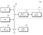
도 20은 본 발명에 따른 반도체 메모리 장치를 포함하는 메모리 시스템을 보여주는 블록도이다. 도 20을 참조하면, 메모리 시스템(700)은 반도체 메모리 장치(710), 전원 장치(720), 중앙처리장치(730), 램(740), 사용자 인터페이스(750), 그리고 시스템 버스(760)를 포함한다.20 is a block diagram showing a memory system including a semiconductor memory device according to the present invention. 20, a
반도체 메모리 장치(710)는 플래시 메모리(711) 및 메모리 컨트롤러(712)를 포함한다. 반도체 메모리 장치(710)는 플래시 메모리 단품을 사용하여 설계될 수도 있고, 원낸드(One NANDTM)와 같이 하나의 집적 회로로 구현될 수도 있다.The
반도체 메모리 장치(710)는 시스템 버스(760)를 통해, 전원 장치(720), 중앙처리장치(730), 램(740), 그리고 유저 인터페이스(750)에 전기적으로 연결된다. 플래시 메모리(711)에는 유저 인터페이스(750)를 통해서 제공되거나 또는 중앙처리장치(730)에 의해서 처리된 데이터가 메모리 컨트롤러(712)를 통해 저장된다.The
만일 반도체 메모리 장치(710)가 반도체 디스크 장치(SSD)로 장착되는 경우, 메모리 시스템(700)의 부팅 속도가 획기적으로 빨라질 것이다. 비록 도면에는 도시되지 않았지만, 도 20에 도시된 메모리 시스템은 응용 칩셋(Application Chipset), 카메라 이미지 프로세서(Camera Image Processor) 등에 사용될 수 있다.If the
본 발명에 따른 반도체 메모리 장치는 다양한 형태들의 패키지를 이용하여 실장될 수 있다. 예를 들면, 본 발명에 따른 플래시 메모리 및/또는 메모리 컨트롤러는 PoP(Package on Package), Ball grid arrays(BGAs), Chip scale packages(CSPs), Plastic Leaded Chip Carrier(PLCC), Plastic Dual In-Line Package(PDIP), Die in Waffle Pack, Die in Wafer Form, Chip On Board(COB), Ceramic Dual In-Line Package(CERDIP), Plastic Metric Quad Flat Pack(MQFP), Thin Quad Flatpack(TQFP), Small Outline(SOIC), Shrink Small Outline Package(SSOP), Thin Small Outline(TSOP), Thin Quad Flatpack(TQFP), System In Package(SIP), Multi Chip Package(MCP), Wafer-level Fabricated Package(WFP), Wafer-Level Processed Stack Package(WSP), 등과 같은 패키지들을 이용하여 실장될 수 있다.The semiconductor memory device according to the present invention can be mounted using various types of packages. For example, the flash memory and / or memory controller according to the present invention can be implemented as a package on package (PoP), ball grid arrays (BGAs), chip scale packages (CSPs), plastic leaded chip carriers Die in Wafer Form, Chip On Board (COB), Ceramic Dual In-Line Package (CERDIP), Plastic Metric Quad Flat Pack (MQFP), Thin Quad Flatpack (TQFP), Small Outline (SOIC), Shrink Small Outline Package (SSOP), Thin Small Outline (TSOP), Thin Quad Flatpack (TQFP), System In Package (SIP), Multi Chip Package (MCP), Wafer-level Fabricated Package -Level Processed Stack Package (WSP), and the like.
한편, 본 발명의 상세한 설명에서는 구체적인 실시 예에 관하여 설명하였으나, 본 발명의 범위에서 벗어나지 않는 한도 내에서 여러 가지 변형이 가능함은 물론이다. 그러므로 본 발명의 범위는 상술한 실시 예에 국한되어 정해져서는 안되며 후술하는 특허청구범위 뿐만 아니라 이 발명의 특허청구범위와 균등한 것들에 의해 정해져야 한다.While the invention has been shown and described with reference to certain preferred embodiments thereof, it will be understood by those skilled in the art that various changes and modifications may be made therein without departing from the spirit and scope of the invention. Therefore, the scope of the present invention should not be limited to the above-described embodiments, but should be determined by the equivalents of the claims of the present invention as well as the claims of the following.
도 1은 본 발명에 따른 플래시 메모리 장치를 예시적으로 보여주는 블록도이다.1 is a block diagram illustrating an exemplary flash memory device according to the present invention.
도 2는 도 1에 도시된 CSL 드라이버를 예시적으로 보여주는 회로도이다.2 is a circuit diagram illustrating an exemplary CSL driver shown in FIG.
도 3은 도 2에 도시된 메모리 셀의 문턱 전압 분포를 보여주는 다이어그램이다.FIG. 3 is a diagram showing a threshold voltage distribution of the memory cell shown in FIG. 2. FIG.
도 4는 제 1 프로그램 상태(P1)의 프로그램 검증 동작과 읽기 동작 시의 문턱 전압 분포를 보여주는 다이어그램이다.4 is a diagram showing a program verify operation in the first program state P1 and a threshold voltage distribution in a read operation.
도 5는 제 2 프로그램 상태(P2)의 프로그램 검증 동작과 읽기 동작 시의 문턱 전압 분포를 보여주는 다이어그램이다.Fig. 5 is a diagram showing the program verify operation in the second program state P2 and the threshold voltage distribution in the read operation.
도 6은 제 3 프로그램 상태(P3)의 프로그램 검증 동작과 읽기 동작 시의 문턱 전압 분포를 보여주는 다이어그램이다.6 is a diagram showing a program verify operation in the third program state P3 and a threshold voltage distribution in a read operation.
도 7은 프로그램 검증 동작과 읽기 동작 시의 공통 소스 라인 전압의 차이로 인한 문턱 전압 분포의 변화를 보여주는 다이어그램이다.7 is a diagram showing a change in a threshold voltage distribution due to a difference between common source line voltages during a program verify operation and a read operation.
도 8은 본 발명에 따른 플래시 메모리 장치의 프로그램 방법을 보여주는 그래프이다.8 is a graph showing a programming method of a flash memory device according to the present invention.
도 9 및 도 10은 본 발명의 프로그램 방법에 따른 영역 분할 방식을 예시적으로 보여주는 다이어그램이다.FIG. 9 and FIG. 10 are diagrams illustrating a method of dividing a region according to the programming method of the present invention.
도 11 내지 도 13은 프로그램 루프에 따라 영역 분할 수를 가변하는 방법을 설명하기 위한 그래프이다.11 to 13 are graphs for explaining a method of varying the number of region divisions according to a program loop.
도 14는 각각의 프로그램 상태에 해당하는 프로그램 데이터의 수를 예시적으로 보여주는 그래프이다.14 is a graph showing an example of the number of program data corresponding to each program state.
도 15는 각각의 프로그램 상태에 해당하는 프로그램 루프를 보여주는 다이어그램이다.15 is a diagram showing a program loop corresponding to each program state.
도 16은 도 1에 도시된 플래시 메모리 장치의 프로그램 루프를 보여주는 그래프이다.16 is a graph showing a program loop of the flash memory device shown in FIG.
도 17 및 도 18은 프로그램 데이터에 따라 영역 분할 수를 조절하는 플래시 메모리 장치를 예시적으로 보여주는 블록도이다.17 and 18 are block diagrams illustrating a flash memory device that adjusts the number of area divisions according to program data.
도 19는 본 발명에 따른 메모리 시스템을 예시적으로 보여주는 블록도이다.19 is a block diagram illustrating an exemplary memory system in accordance with the present invention.
도 20은 본 발명에 따른 반도체 메모리 장치를 포함하는 메모리 시스템을 보여주는 블록도이다.20 is a block diagram showing a memory system including a semiconductor memory device according to the present invention.
Claims (13)
Translated fromKoreanPriority Applications (2)
| Application Number | Priority Date | Filing Date | Title |
|---|---|---|---|
| KR1020080077033AKR101427896B1 (en) | 2008-08-06 | 2008-08-06 | A flash memory device for reducing noise in a common source line and a memory system including the same |
| US12/533,720US8068361B2 (en) | 2008-08-06 | 2009-07-31 | Systems and methods for performing a program-verify process on a nonvolatile memory by selectively pre-charging bit lines associated with memory cells during the verify operations |
Applications Claiming Priority (1)
| Application Number | Priority Date | Filing Date | Title |
|---|---|---|---|
| KR1020080077033AKR101427896B1 (en) | 2008-08-06 | 2008-08-06 | A flash memory device for reducing noise in a common source line and a memory system including the same |
Publications (2)
| Publication Number | Publication Date |
|---|---|
| KR20100018318A KR20100018318A (en) | 2010-02-17 |
| KR101427896B1true KR101427896B1 (en) | 2014-08-11 |
Family
ID=41652812
Family Applications (1)
| Application Number | Title | Priority Date | Filing Date |
|---|---|---|---|
| KR1020080077033AActiveKR101427896B1 (en) | 2008-08-06 | 2008-08-06 | A flash memory device for reducing noise in a common source line and a memory system including the same |
Country Status (2)
| Country | Link |
|---|---|
| US (1) | US8068361B2 (en) |
| KR (1) | KR101427896B1 (en) |
Families Citing this family (26)
| Publication number | Priority date | Publication date | Assignee | Title |
|---|---|---|---|---|
| KR20110131648A (en) | 2010-05-31 | 2011-12-07 | 삼성전자주식회사 | Non-volatile memory device, memory system and memory card including it and program method thereof |
| US8274838B2 (en) | 2010-07-19 | 2012-09-25 | Sandisk Technologies Inc. | Programming non-volatile memory with bit line voltage step up |
| TW201225088A (en)* | 2010-07-21 | 2012-06-16 | Mosaid Technologies Inc | Multipage program scheme for flash memory |
| KR20120030281A (en) | 2010-09-20 | 2012-03-28 | 삼성전자주식회사 | Flash memory device and program verification method thereof |
| KR101752168B1 (en) | 2010-11-24 | 2017-06-30 | 삼성전자주식회사 | Nonvolatile memory device, method of operating the same, and electronic device having the same |
| KR101861084B1 (en) | 2011-07-11 | 2018-05-28 | 삼성전자주식회사 | Nonvolatile memory device, method of operating the same, and electronic device having the same |
| KR101775660B1 (en) | 2011-09-29 | 2017-09-07 | 삼성전자주식회사 | Method of reading memory cells with different threshold voltages without variation of word line voltage and nonvolatile memory device using the same |
| US8711619B2 (en) | 2011-10-18 | 2014-04-29 | Seagate Technology Llc | Categorizing bit errors of solid-state, non-volatile memory |
| US8737133B2 (en) | 2011-10-18 | 2014-05-27 | Seagate Technology Llc | Shifting cell voltage based on grouping of solid-state, non-volatile memory cells |
| US8693257B2 (en) | 2011-10-18 | 2014-04-08 | Seagate Technology Llc | Determining optimal read reference and programming voltages for non-volatile memory using mutual information |
| US8760932B2 (en)* | 2011-10-18 | 2014-06-24 | Seagate Technology Llc | Determination of memory read reference and programming voltages |
| US8842476B2 (en) | 2011-11-09 | 2014-09-23 | Sandisk Technologies Inc. | Erratic program detection for non-volatile storage |
| US8630118B2 (en) | 2011-11-09 | 2014-01-14 | Sandisk Technologies Inc. | Defective word line detection |
| US10170187B2 (en) | 2012-04-02 | 2019-01-01 | Micron Technology, Inc. | Apparatuses and methods using negative voltages in part of memory write read, and erase operations |
| DE102013105356A1 (en) | 2012-05-29 | 2013-12-05 | Samsung Electronics Co., Ltd. | Method for operating non-volatile memory device for use in smart-TV system, involves detecting errors generated during programming operation for programming portion of non-volatile multi-bit memory cells in non-volatile memory device |
| KR101996004B1 (en) | 2012-05-29 | 2019-07-03 | 삼성전자주식회사 | Programming method of nonvolatile memory device and memory system having the same |
| CN103019616B (en)* | 2012-11-23 | 2015-11-25 | 记忆科技(深圳)有限公司 | The charge/discharge control method of a kind of solid state hard disc and flash chip |
| KR102030326B1 (en) | 2013-01-21 | 2019-10-10 | 삼성전자 주식회사 | Nonvolatile memory device and driving method thereof |
| US9135109B2 (en) | 2013-03-11 | 2015-09-15 | Seagate Technology Llc | Determination of optimum threshold voltage to read data values in memory cells |
| US9064569B1 (en)* | 2014-07-03 | 2015-06-23 | Sandisk Technologies Inc. | Memory controller with resistive random access memory (ReRAM) |
| KR102238579B1 (en)* | 2014-08-06 | 2021-04-09 | 삼성전자주식회사 | Method of programming memory device |
| KR20160060917A (en)* | 2014-11-21 | 2016-05-31 | 에스케이하이닉스 주식회사 | Non-volatile memory device and method of programing the same |
| KR20160108770A (en)* | 2015-03-06 | 2016-09-20 | 에스케이하이닉스 주식회사 | Semiconductor memory device and operating method thereof |
| KR20170026831A (en)* | 2015-08-28 | 2017-03-09 | 에스케이하이닉스 주식회사 | Nonvolatile memory device, data storage device including thereof and operating method for data storage device |
| KR20210024916A (en)* | 2019-08-26 | 2021-03-08 | 에스케이하이닉스 주식회사 | Memory device and operating method thereof |
| JP2021047953A (en) | 2019-09-19 | 2021-03-25 | キオクシア株式会社 | Semiconductor storage device |
Citations (4)
| Publication number | Priority date | Publication date | Assignee | Title |
|---|---|---|---|---|
| US6125052A (en) | 1997-09-18 | 2000-09-26 | Kabushiki Kaisha Toshiba | Semiconductor memory device |
| KR20040057536A (en)* | 2002-12-26 | 2004-07-02 | 주식회사 하이닉스반도체 | Method of programing a flash memory device |
| US20060221688A1 (en) | 1999-02-01 | 2006-10-05 | Shoji Shukuri | Semiconductor integrated circuit and nonvolatile memory element |
| KR20080009073A (en)* | 2005-04-01 | 2008-01-24 | 쌘디스크 코포레이션 | Nonvolatile Memory and Source Line Bias Errors Compensation Method |
Family Cites Families (5)
| Publication number | Priority date | Publication date | Assignee | Title |
|---|---|---|---|---|
| JPH11176182A (en) | 1997-12-09 | 1999-07-02 | Toshiba Corp | Nonvolatile semiconductor memory device |
| KR19990048771A (en) | 1997-12-10 | 1999-07-05 | 김영환 | Programming method in word mode in flash memory |
| JP2000048582A (en) | 1998-07-28 | 2000-02-18 | Toshiba Corp | Semiconductor storage device |
| US7362084B2 (en)* | 2005-03-14 | 2008-04-22 | Silicon Storage Technology, Inc. | Fast voltage regulators for charge pumps |
| US7330376B1 (en)* | 2006-07-27 | 2008-02-12 | Macronix International Co., Ltd. | Method for memory data storage by partition into narrower threshold voltage distribution regions |
- 2008
- 2008-08-06KRKR1020080077033Apatent/KR101427896B1/enactiveActive
- 2009
- 2009-07-31USUS12/533,720patent/US8068361B2/ennot_activeExpired - Fee Related
Patent Citations (4)
| Publication number | Priority date | Publication date | Assignee | Title |
|---|---|---|---|---|
| US6125052A (en) | 1997-09-18 | 2000-09-26 | Kabushiki Kaisha Toshiba | Semiconductor memory device |
| US20060221688A1 (en) | 1999-02-01 | 2006-10-05 | Shoji Shukuri | Semiconductor integrated circuit and nonvolatile memory element |
| KR20040057536A (en)* | 2002-12-26 | 2004-07-02 | 주식회사 하이닉스반도체 | Method of programing a flash memory device |
| KR20080009073A (en)* | 2005-04-01 | 2008-01-24 | 쌘디스크 코포레이션 | Nonvolatile Memory and Source Line Bias Errors Compensation Method |
Also Published As
| Publication number | Publication date |
|---|---|
| KR20100018318A (en) | 2010-02-17 |
| US8068361B2 (en) | 2011-11-29 |
| US20100034019A1 (en) | 2010-02-11 |
Similar Documents
| Publication | Publication Date | Title |
|---|---|---|
| KR101427896B1 (en) | A flash memory device for reducing noise in a common source line and a memory system including the same | |
| KR101434399B1 (en) | Flash memory device reducing noise of common source line, program verify method thereof, and memory system including that | |
| US10573378B2 (en) | Methods of programming memory devices | |
| US9064581B2 (en) | Method of programming non-volatile memory device and non-volatile memory device using the same | |
| KR101669550B1 (en) | Flash memory device reducing noise of common source line, operating method thereof, and memory system including that | |
| JP5780824B2 (en) | Nonvolatile memory device and program method thereof | |
| KR102336661B1 (en) | Non-volatile memory device and sensing method thereof | |
| KR102122239B1 (en) | Non-volatile memory device and program method of the same | |
| KR101980676B1 (en) | Memory and method for verifying the same | |
| KR100882206B1 (en) | Nonvolatile Memory Device and Its Operation Method | |
| US9564227B2 (en) | Memory device having a different source line coupled to each of a plurality of layers of memory cell arrays | |
| KR101462489B1 (en) | Program method and initial charging method of nonvolatile memory device | |
| KR20100013189A (en) | Nonvolatile memory device and programmming method teherof | |
| US9251901B2 (en) | Semiconductor memory device with high threshold voltage distribution reliability method | |
| KR101435889B1 (en) | Flash memory device controlling common source line voltage, program verify method thereof, and memory system including that | |
| JP2002133888A (en) | Nonvolatile semiconductor memory device | |
| KR20170056254A (en) | Nonvolatile memory device | |
| KR20140021909A (en) | Semiconductor memory device and operating method thereof | |
| KR20240075511A (en) | Semiconductor device performing program operation and operating method thereof | |
| KR20230073066A (en) | Memory device for individually applying voltages to word lines adjacent to a selected word line, and method of operating the same |
Legal Events
| Date | Code | Title | Description |
|---|---|---|---|
| PA0109 | Patent application | St.27 status event code:A-0-1-A10-A12-nap-PA0109 | |
| P11-X000 | Amendment of application requested | St.27 status event code:A-2-2-P10-P11-nap-X000 | |
| P13-X000 | Application amended | St.27 status event code:A-2-2-P10-P13-nap-X000 | |
| R15-X000 | Change to inventor requested | St.27 status event code:A-3-3-R10-R15-oth-X000 | |
| R16-X000 | Change to inventor recorded | St.27 status event code:A-3-3-R10-R16-oth-X000 | |
| PG1501 | Laying open of application | St.27 status event code:A-1-1-Q10-Q12-nap-PG1501 | |
| R18-X000 | Changes to party contact information recorded | St.27 status event code:A-3-3-R10-R18-oth-X000 | |
| A201 | Request for examination | ||
| PA0201 | Request for examination | St.27 status event code:A-1-2-D10-D11-exm-PA0201 | |
| E701 | Decision to grant or registration of patent right | ||
| PE0701 | Decision of registration | St.27 status event code:A-1-2-D10-D22-exm-PE0701 | |
| GRNT | Written decision to grant | ||
| PR0701 | Registration of establishment | St.27 status event code:A-2-4-F10-F11-exm-PR0701 | |
| PR1002 | Payment of registration fee | St.27 status event code:A-2-2-U10-U11-oth-PR1002 Fee payment year number:1 | |
| PG1601 | Publication of registration | St.27 status event code:A-4-4-Q10-Q13-nap-PG1601 | |
| PR1001 | Payment of annual fee | St.27 status event code:A-4-4-U10-U11-oth-PR1001 Fee payment year number:4 | |
| FPAY | Annual fee payment | Payment date:20180731 Year of fee payment:5 | |
| PR1001 | Payment of annual fee | St.27 status event code:A-4-4-U10-U11-oth-PR1001 Fee payment year number:5 | |
| FPAY | Annual fee payment | Payment date:20190731 Year of fee payment:6 | |
| PR1001 | Payment of annual fee | St.27 status event code:A-4-4-U10-U11-oth-PR1001 Fee payment year number:6 | |
| PR1001 | Payment of annual fee | St.27 status event code:A-4-4-U10-U11-oth-PR1001 Fee payment year number:7 | |
| PR1001 | Payment of annual fee | St.27 status event code:A-4-4-U10-U11-oth-PR1001 Fee payment year number:8 | |
| PR1001 | Payment of annual fee | St.27 status event code:A-4-4-U10-U11-oth-PR1001 Fee payment year number:9 | |
| PR1001 | Payment of annual fee | St.27 status event code:A-4-4-U10-U11-oth-PR1001 Fee payment year number:10 | |
| PR1001 | Payment of annual fee | St.27 status event code:A-4-4-U10-U11-oth-PR1001 Fee payment year number:11 | |
| PR1001 | Payment of annual fee | St.27 status event code:A-4-4-U10-U11-oth-PR1001 Fee payment year number:12 |