KR101427502B1 - Method for manufacturing a metal oxide semiconductor - Google Patents
Method for manufacturing a metal oxide semiconductorDownload PDFInfo
- Publication number
- KR101427502B1 KR101427502B1KR1020127026567AKR20127026567AKR101427502B1KR 101427502 B1KR101427502 B1KR 101427502B1KR 1020127026567 AKR1020127026567 AKR 1020127026567AKR 20127026567 AKR20127026567 AKR 20127026567AKR 101427502 B1KR101427502 B1KR 101427502B1
- Authority
- KR
- South Korea
- Prior art keywords
- alkoxide
- thin film
- oxide semiconductor
- metal oxide
- film transistor
- Prior art date
- Legal status (The legal status is an assumption and is not a legal conclusion. Google has not performed a legal analysis and makes no representation as to the accuracy of the status listed.)
- Expired - Fee Related
Links
Images


Classifications
- C—CHEMISTRY; METALLURGY
- C23—COATING METALLIC MATERIAL; COATING MATERIAL WITH METALLIC MATERIAL; CHEMICAL SURFACE TREATMENT; DIFFUSION TREATMENT OF METALLIC MATERIAL; COATING BY VACUUM EVAPORATION, BY SPUTTERING, BY ION IMPLANTATION OR BY CHEMICAL VAPOUR DEPOSITION, IN GENERAL; INHIBITING CORROSION OF METALLIC MATERIAL OR INCRUSTATION IN GENERAL
- C23C—COATING METALLIC MATERIAL; COATING MATERIAL WITH METALLIC MATERIAL; SURFACE TREATMENT OF METALLIC MATERIAL BY DIFFUSION INTO THE SURFACE, BY CHEMICAL CONVERSION OR SUBSTITUTION; COATING BY VACUUM EVAPORATION, BY SPUTTERING, BY ION IMPLANTATION OR BY CHEMICAL VAPOUR DEPOSITION, IN GENERAL
- C23C18/00—Chemical coating by decomposition of either liquid compounds or solutions of the coating forming compounds, without leaving reaction products of surface material in the coating; Contact plating
- C23C18/02—Chemical coating by decomposition of either liquid compounds or solutions of the coating forming compounds, without leaving reaction products of surface material in the coating; Contact plating by thermal decomposition
- C23C18/12—Chemical coating by decomposition of either liquid compounds or solutions of the coating forming compounds, without leaving reaction products of surface material in the coating; Contact plating by thermal decomposition characterised by the deposition of inorganic material other than metallic material
- C23C18/1204—Chemical coating by decomposition of either liquid compounds or solutions of the coating forming compounds, without leaving reaction products of surface material in the coating; Contact plating by thermal decomposition characterised by the deposition of inorganic material other than metallic material inorganic material, e.g. non-oxide and non-metallic such as sulfides, nitrides based compounds
- C23C18/1208—Oxides, e.g. ceramics
- C23C18/1216—Metal oxides
- C—CHEMISTRY; METALLURGY
- C23—COATING METALLIC MATERIAL; COATING MATERIAL WITH METALLIC MATERIAL; CHEMICAL SURFACE TREATMENT; DIFFUSION TREATMENT OF METALLIC MATERIAL; COATING BY VACUUM EVAPORATION, BY SPUTTERING, BY ION IMPLANTATION OR BY CHEMICAL VAPOUR DEPOSITION, IN GENERAL; INHIBITING CORROSION OF METALLIC MATERIAL OR INCRUSTATION IN GENERAL
- C23C—COATING METALLIC MATERIAL; COATING MATERIAL WITH METALLIC MATERIAL; SURFACE TREATMENT OF METALLIC MATERIAL BY DIFFUSION INTO THE SURFACE, BY CHEMICAL CONVERSION OR SUBSTITUTION; COATING BY VACUUM EVAPORATION, BY SPUTTERING, BY ION IMPLANTATION OR BY CHEMICAL VAPOUR DEPOSITION, IN GENERAL
- C23C18/00—Chemical coating by decomposition of either liquid compounds or solutions of the coating forming compounds, without leaving reaction products of surface material in the coating; Contact plating
- C23C18/02—Chemical coating by decomposition of either liquid compounds or solutions of the coating forming compounds, without leaving reaction products of surface material in the coating; Contact plating by thermal decomposition
- C23C18/12—Chemical coating by decomposition of either liquid compounds or solutions of the coating forming compounds, without leaving reaction products of surface material in the coating; Contact plating by thermal decomposition characterised by the deposition of inorganic material other than metallic material
- C23C18/125—Process of deposition of the inorganic material
- C23C18/1283—Control of temperature, e.g. gradual temperature increase, modulation of temperature
- H—ELECTRICITY
- H01—ELECTRIC ELEMENTS
- H01L—SEMICONDUCTOR DEVICES NOT COVERED BY CLASS H10
- H01L21/00—Processes or apparatus adapted for the manufacture or treatment of semiconductor or solid state devices or of parts thereof
- H01L21/02—Manufacture or treatment of semiconductor devices or of parts thereof
- H01L21/02104—Forming layers
- H01L21/02365—Forming inorganic semiconducting materials on a substrate
- H01L21/02518—Deposited layers
- H01L21/02521—Materials
- H01L21/02551—Group 12/16 materials
- H01L21/02554—Oxides
- H—ELECTRICITY
- H01—ELECTRIC ELEMENTS
- H01L—SEMICONDUCTOR DEVICES NOT COVERED BY CLASS H10
- H01L21/00—Processes or apparatus adapted for the manufacture or treatment of semiconductor or solid state devices or of parts thereof
- H01L21/02—Manufacture or treatment of semiconductor devices or of parts thereof
- H01L21/02104—Forming layers
- H01L21/02365—Forming inorganic semiconducting materials on a substrate
- H01L21/02518—Deposited layers
- H01L21/02521—Materials
- H01L21/02565—Oxide semiconducting materials not being Group 12/16 materials, e.g. ternary compounds
- H—ELECTRICITY
- H01—ELECTRIC ELEMENTS
- H01L—SEMICONDUCTOR DEVICES NOT COVERED BY CLASS H10
- H01L21/00—Processes or apparatus adapted for the manufacture or treatment of semiconductor or solid state devices or of parts thereof
- H01L21/02—Manufacture or treatment of semiconductor devices or of parts thereof
- H01L21/02104—Forming layers
- H01L21/02365—Forming inorganic semiconducting materials on a substrate
- H01L21/02612—Formation types
- H01L21/02617—Deposition types
- H01L21/02623—Liquid deposition
- H01L21/02628—Liquid deposition using solutions
- H—ELECTRICITY
- H01—ELECTRIC ELEMENTS
- H01L—SEMICONDUCTOR DEVICES NOT COVERED BY CLASS H10
- H01L21/00—Processes or apparatus adapted for the manufacture or treatment of semiconductor or solid state devices or of parts thereof
- H01L21/02—Manufacture or treatment of semiconductor devices or of parts thereof
- H01L21/04—Manufacture or treatment of semiconductor devices or of parts thereof the devices having potential barriers, e.g. a PN junction, depletion layer or carrier concentration layer
- H01L21/18—Manufacture or treatment of semiconductor devices or of parts thereof the devices having potential barriers, e.g. a PN junction, depletion layer or carrier concentration layer the devices having semiconductor bodies comprising elements of Group IV of the Periodic Table or AIIIBV compounds with or without impurities, e.g. doping materials
- H01L21/30—Treatment of semiconductor bodies using processes or apparatus not provided for in groups H01L21/20 - H01L21/26
- H01L21/324—Thermal treatment for modifying the properties of semiconductor bodies, e.g. annealing, sintering
- H—ELECTRICITY
- H10—SEMICONDUCTOR DEVICES; ELECTRIC SOLID-STATE DEVICES NOT OTHERWISE PROVIDED FOR
- H10D—INORGANIC ELECTRIC SEMICONDUCTOR DEVICES
- H10D30/00—Field-effect transistors [FET]
- H10D30/01—Manufacture or treatment
- H10D30/021—Manufacture or treatment of FETs having insulated gates [IGFET]
- H10D30/031—Manufacture or treatment of FETs having insulated gates [IGFET] of thin-film transistors [TFT]
- H—ELECTRICITY
- H10—SEMICONDUCTOR DEVICES; ELECTRIC SOLID-STATE DEVICES NOT OTHERWISE PROVIDED FOR
- H10D—INORGANIC ELECTRIC SEMICONDUCTOR DEVICES
- H10D30/00—Field-effect transistors [FET]
- H10D30/60—Insulated-gate field-effect transistors [IGFET]
- H10D30/67—Thin-film transistors [TFT]
- H10D30/674—Thin-film transistors [TFT] characterised by the active materials
- H10D30/6755—Oxide semiconductors, e.g. zinc oxide, copper aluminium oxide or cadmium stannate
- H—ELECTRICITY
- H10—SEMICONDUCTOR DEVICES; ELECTRIC SOLID-STATE DEVICES NOT OTHERWISE PROVIDED FOR
- H10D—INORGANIC ELECTRIC SEMICONDUCTOR DEVICES
- H10D99/00—Subject matter not provided for in other groups of this subclass
- H—ELECTRICITY
- H10—SEMICONDUCTOR DEVICES; ELECTRIC SOLID-STATE DEVICES NOT OTHERWISE PROVIDED FOR
- H10D—INORGANIC ELECTRIC SEMICONDUCTOR DEVICES
- H10D86/00—Integrated devices formed in or on insulating or conducting substrates, e.g. formed in silicon-on-insulator [SOI] substrates or on stainless steel or glass substrates
- H10D86/01—Manufacture or treatment
- H10D86/021—Manufacture or treatment of multiple TFTs
- H10D86/0241—Manufacture or treatment of multiple TFTs using liquid deposition, e.g. printing
Landscapes
- Chemical & Material Sciences (AREA)
- Engineering & Computer Science (AREA)
- Physics & Mathematics (AREA)
- Condensed Matter Physics & Semiconductors (AREA)
- General Physics & Mathematics (AREA)
- Manufacturing & Machinery (AREA)
- Computer Hardware Design (AREA)
- Microelectronics & Electronic Packaging (AREA)
- Power Engineering (AREA)
- Thermal Sciences (AREA)
- Inorganic Chemistry (AREA)
- General Chemical & Material Sciences (AREA)
- Chemical Kinetics & Catalysis (AREA)
- Materials Engineering (AREA)
- Mechanical Engineering (AREA)
- Metallurgy (AREA)
- Organic Chemistry (AREA)
- Ceramic Engineering (AREA)
- Thin Film Transistor (AREA)
- Liquid Deposition Of Substances Of Which Semiconductor Devices Are Composed (AREA)
Abstract
Translated fromKoreanDescription
Translated fromKorean본 발명은 금속 산화물 반도체 및, 상세하게는, 금속 산화물 반도체 제조 방법에 관한 것이다.The present invention relates to a metal oxide semiconductor and, more particularly, to a method for manufacturing a metal oxide semiconductor.
종래의 박막 트랜지스터(TFT)는, 반도체 층에서, 비정질 실리콘 박막 및, 엑시머 레이저 등을 이용하여 비정질 실리콘 박막의 다결정화를 통해 형성된 다결정 실리콘 박막과 같은 실리콘을 주로 이용한다.A conventional thin film transistor (TFT) mainly uses silicon such as a polycrystalline silicon thin film formed through polycrystallization of an amorphous silicon thin film by using an amorphous silicon thin film and an excimer laser in the semiconductor layer.
최근, 비정질 금속 산화물 반도체는 차세대 TFT를 위한 반도체 층으로 주목받고 있다. 투명도에 있어서, 이러한 반도체는, 디스플레이, 전자 종이 등에 대한 적용 가능성을 보여준다. 심지어 이동도에 있어서, 이러한 반도체는, 또한, 고성능 액정 및 유기 전계 발광(EL)에 의해 요구되는 3cm2/Vs 내지 20cm2/Vs를 실현할 수 있는 재료이다.In recent years, amorphous metal oxide semiconductors have attracted attention as semiconductor layers for next generation TFTs. In terms of transparency, such semiconductors show applicability to displays, electronic paper, and the like. Even in the mobility, such a semiconductor is, also, a material that can realize a 3cm2 / Vs to about 20cm2 / Vs required by high-performance liquid crystal and organic electroluminescent (EL).
인듐(In) 및 아연(Zn)을 함유하는 비정질 인듐 아연 산화물 반도체(a-InZnO), 갈륨(Ga)을 금속 성분의 추가 형태로 더 포함하는 비정질 인듐 갈륨 아연 산화물 반도체(a-InGaZnO) 등은 비정질 금속 산화물 반도체들의 대표격으로 알려져 있다.An amorphous indium zinc oxide semiconductor (a-InZnO) containing indium (In) and zinc (Zn) and an amorphous indium gallium zinc oxide semiconductor (a-InGaZnO) further including gallium (Ga) Amorphous metal oxide semiconductors.
한편, 증기로부터 막을 형성하는 스퍼터링(sputtering) 방법 및 용액으로부터 막을 형성하는 졸겔 방법은 반도체 층을 제조하는 대표적인 방법이다(예컨대, 특허문헌 1, 2 및 3을 참조). 졸겔 방법은 넓은 표면적을 가지는 기판 및 복합 형상을 가지는 기판에 적용가능한 것을 특징으로 한다.On the other hand, a sputtering method of forming a film from a vapor and a sol-gel method of forming a film from a solution are representative methods of manufacturing a semiconductor layer (see, for example,
졸겔 방법은 용액이 금속 산화물의 각 금속 성분에 대한 가수분해성 유기 화합물인 전구체를 함유하도록 제조되는 방법이며, 이 용액은 가수분해 반응 및 축중합 반응을 겪어서 유동성을 잃은 겔을 형성하고, 이 겔은 열 어닐링되어 고체 금속 산화물을 얻는다. 금속 알콕사이드 및 이와 같은 것은 전구체로서 주어진다. 가수분해 반응을 위한 물 및 가수분해 반응과 축중합 반응을 제어하기 위한 산, 염기 등과 같은 촉매가 전구체 용액에 또한 추가된다.The sol-gel process is a process wherein the solution is prepared to contain a precursor which is a hydrolyzable organic compound for each metal component of the metal oxide, which undergoes hydrolysis and polycondensation reactions to form a gel that has lost flowability, Heat-annealed to obtain a solid metal oxide. Metal alkoxides and the like are given as precursors. Water for the hydrolysis reaction and catalysts such as acids, bases and the like for controlling the hydrolysis and condensation reactions are also added to the precursor solution.
[인용목록][Citation List]
[특허문헌][Patent Literature]
[특허문헌 1] 일본 공개 특허 공보 No. 2006-165529[Patent Document 1] Japanese Unexamined Patent Publication No. Hei. 2006-165529
[특허문헌 2] 일본 공개 특허 공보 No. 2003-179242[Patent Document 2] Japanese Unexamined Patent Publication No. Hei. 2003-179242
[특허문헌 3] 일본 공개 특허 공보 No. 2005-223231[Patent Document 3] Japanese Unexamined Patent Publication No. Hei. 2005-223231
그러나 전구체 용액이 기판에 증착되고 이 전구체 용액이 대기에서 열 어닐링되어 졸겔 방법을 사용하여 비정질 금속 산화물 반도체의 박막을 형성하는 경우 이하의 문제점들이 존재한다.However, the following problems exist when a precursor solution is deposited on a substrate and the precursor solution is thermally annealed in the atmosphere to form a thin film of an amorphous metal oxide semiconductor using a sol-gel method.
먼저, 기판에 전구체 용액이 증착되기 전 저장용기의 전구체 용액에 물이 추가되는 경우, 물과 전구체는 전구체 용액이 저장용기에 있는 동안 반응을 시작한다. 저장 용기에서 가수분해 반응 및 축중합 반응을 겪은 뒤, 전구체 용액은 유동성은 잃고 높은 점도를 갖는 겔로 변한다. 이처럼, 증착에 의해서 기판상에 박막을 형성하는 것은 어렵다. 게다가, 연장된 시간 기간 동안 전구체 용액을 저장하는 경우, 축중합 반응이 추가로 진행되고 고체 금속 산화물이 전구체 용액에서 생성된다. 그러므로 전구체 용액의 저장을 연장하는 것은 어렵다.First, when water is added to the precursor solution of the storage vessel before the precursor solution is deposited on the substrate, the water and the precursor begin to react while the precursor solution is in the storage vessel. After experiencing the hydrolysis and polycondensation reactions in the storage vessel, the precursor solution turns into a gel that has lost its fluidity and has a high viscosity. As described above, it is difficult to form a thin film on a substrate by vapor deposition. In addition, when storing the precursor solution for an extended period of time, the condensation polymerization proceeds further and a solid metal oxide is produced in the precursor solution. It is therefore difficult to extend the storage of the precursor solution.
게다가, 전구체 용액에 물을 추가하지 않고 막을 형성하는 경우, 전구체의 가수분해는 대기에 포함된 습기로 인해 일어나지만, 부족한 양의 물이 공급되어서 충분히 일어나지 않는다. 전구체는 가열에 의해 분해될 수 있으나, 약 400℃ 이상에서의 고온 처리가 요구된다. 이러한 경우, 플라스틱 기판처럼 비교적 낮은 내열성을 가지는 기판을 사용하는 것은 불가능하다.Furthermore, when forming a film without adding water to the precursor solution, the hydrolysis of the precursor takes place due to the moisture contained in the atmosphere, but a sufficient amount of water is not supplied sufficiently. Precursors can be decomposed by heating, but high temperature treatment at about 400 캜 or higher is required. In this case, it is impossible to use a substrate having a relatively low heat resistance such as a plastic substrate.
결과적으로, 상술한 문제점들의 관점에서, 본 발명의 목적은 저온에서 금속 산화물 반도체의 박막을 형성하는 방법을 제공하는 것이다.Consequently, in view of the above-mentioned problems, it is an object of the present invention to provide a method of forming a thin film of a metal oxide semiconductor at a low temperature.
상기 언급된 목적을 달성하기 위해, 본 발명의 측면에 따른 금속 산화물 반도체를 제조하는 방법은: 용매 내의 적어도 하나는 금속 알콕사이드인 적어도 2개의 전구체들의 혼합 용액으로부터 막을 기판에 증착하는 단계, 및 혼합 용액으로부터 금속 산화물 반도체를 형성하기 위해, 수성 촉매가 존재하는 경우에 이를 포함하여 기판상에 증착된 막을 경화(curing)하는 단계를 포함한다.In order to achieve the above-mentioned object, a method of manufacturing a metal-oxide semiconductor according to aspects of the present invention includes: depositing a film from a mixed solution of at least two precursors in a solvent, the at least one being a metal alkoxide, And curing the film deposited on the substrate, if any, in the presence of an aqueous catalyst to form a metal oxide semiconductor from the substrate.
본 발명의 측면에 따르면, 금속 산화물의 박막은 저온에서 형성될 수 있다.According to aspects of the present invention, a thin film of a metal oxide can be formed at a low temperature.
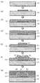
도 1은 본 발명의 일 실시예에 따른 박막 트랜지스터 디바이스를 제조하는 방법을 도식적으로 설명하기 위한 단면도이다.
도 2는 실시예에 따른 박막 트랜지스터 디바이스를 제조하기 위한 방법에서 비정질 금속 산화물 반도체 층을 형성하는 처리(도 1의 (d)에 도시된 처리)의 세부사항을 도시하는 단면도이다.
도 3a는 비정질 금속 산화물 반도체 층의 깊이방향으로의 탄소 및 수소의 농도 분포를 도시하는 그래프이다.
도 3b는 비정질 금속 산화물 반도체 층의 투과율의 파장 의존성을 도시하는 그래프이다.
도 3c는 인듐 알콕사이드 용액 질량의 시간 변화(생성된 가스의 양에 대한 시간변화)를 도시하는 그래프이다.
도 3d는 아연 알콕사이드 용액 질량의 시간 변화(생성된 가스의 양에 대한 시간변화)를 도시하는 그래프이다.
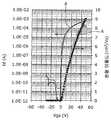
도 4a는 실시예에 따른 박막 트랜지스터 디바이스의 이동도와 드레인 전류의 게이트 전압 의존성을 도시하는 그래프이다.
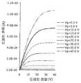
도 4b는 각각의 상이한 게이트 전압에 대한 박막 트랜지스터 디바이스의 드레인 전류의 드레인 전압 의존성을 도시하는 그래프이다.
도 4c는 비교 예시로서 박막 트랜지스터 디바이스의 이동도 및 드레인 전류의 게이트 전압 의존성을 도시하는 그래프이다.
도 4d는 비교 예시로서 박막 트랜지스터 디바이스의 이동도 및 드레인 전류의 게이트 전압 의존성을 도시하는 그래프이다.
도 4e는 비교 예시로서 박막 트랜지스터 디바이스의 이동도 및 드레인 전류의 게이트 전압 의존성을 도시하는 그래프이다.
도 5a는 실시예에 따른 박막 트랜지스터 디바이스의 이동도 및 드레인 전류의 게이트 전압 의존성을 도시하는 그래프이다.
도 5b는 실시예에 따른 박막 트랜지스터 디바이스의 이동도 및 드레인 전류의 게이트 전압 의존성을 도시하는 그래프이다.
도 5c는 실시예에 따른 박막 트랜지스터 디바이스의 이동도 및 드레인 전류의 게이트 전압 의존성을 도시하는 그래프이다.
도 5d는 실시예에 따른 박막 트랜지스터 디바이스의 이동도 및 드레인 전류의 게이트 전압 의존성을 도시하는 그래프이다.
도 5e는 실시예에 따른 박막 트랜지스터 디바이스의 이동도 및 드레인 전류의 게이트 전압 의존성을 도시하는 그래프이다.
도 5f는 실시예에 따른 박막 트랜지스터 디바이스의 이동도 및 드레인 전류의 게이트 전압 의존성을 도시하는 그래프이다.
도 6a는 실시예에 따른 박막 트랜지스터 디바이스의 이동도의 열 어닐링 온도 의존성을 도시하는 그래프이다.
도 6b는 실시예에 따른 박막 트랜지스터 디바이스의 히스테리시스의 열 어닐링 온도 의존성을 도시하는 그래프이다.
도 6c는 실시예에 따른 박막 트랜지스터 디바이스의 턴온 전압의 열 어닐링 온도 의존성을 도시하는 그래프이다.
도 7a는 실시예에 따른 박막 트랜지스터 디바이스의 이동도 및 드레인 전류의 게이트 전압 의존성을 도시하는 그래프이다.
도 7b는 실시예에 따른 박막 트랜지스터 디바이스의 이동도 및 드레인 전류의 게이트 전압 의존성을 도시하는 그래프이다.
도 7c는 실시예에 따른 박막 트랜지스터 디바이스의 이동도 및 드레인 전류의 게이트 전압 의존성을 도시하는 그래프이다.
도 7d는 실시예에 따른 박막 트랜지스터 디바이스의 이동도 및 드레인 전류의 게이트 전압 의존성을 도시하는 그래프이다.
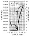
도 8은 실시예에 따른 졸겔 반응에서의 열 어닐링 온도에 대한 시간변화를 도시하는 그래프이다.
도 9a는 실시예에 따른 박막 트랜지스터 디바이스의 이동도 및 드레인 전류의 게이트 전압 의존성을 도시하는 그래프이다.
도 9b는 실시예에 따른 박막 트랜지스터 디바이스의 이동도 및 드레인 전류의 게이트 전압 의존성을 도시하는 그래프이다.
도 9c는 실시예에 따른 박막 트랜지스터 디바이스의 이동도 및 드레인 전류의 게이트 전압 의존성을 도시하는 그래프이다.
도 9d는 실시예에 따른 박막 트랜지스터 디바이스의 이동도 및 드레인 전류의 게이트 전압 의존성을 도시하는 그래프이다.
도 9e는 실시예에 따른 박막 트랜지스터 디바이스의 이동도 및 드레인 전류의 게이트 전압 의존성을 도시하는 그래프이다.
도 9f는 실시예에 따른 박막 트랜지스터 디바이스의 이동도 및 드레인 전류의 게이트 전압 의존성을 도시하는 그래프이다.
도 10은 실시예에 따른 졸겔 반응에서의 열 어닐링 온도에 대한 시간변화를 도시하는 그래프이다.
도 11a는 실시예에 따른 박막 트랜지스터 디바이스의 이동도 및 드레인 전류의 게이트 전압 의존성을 도시하는 그래프이다.
도 11b는 실시예에 따른 박막 트랜지스터 디바이스의 이동도 및 드레인 전류의 게이트 전압 의존성을 도시하는 그래프이다.
도 11c는 실시예에 따른 박막 트랜지스터 디바이스의 이동도 및 드레인 전류의 게이트 전압 의존성을 도시하는 그래프이다.
도 11d는 실시예에 따른 박막 트랜지스터 디바이스의 이동도 및 드레인 전류의 게이트 전압 의존성을 도시하는 그래프이다.
도 11e는 실시예에 따른 박막 트랜지스터 디바이스의 이동도 및 드레인 전류의 게이트 전압 의존성을 도시하는 그래프이다.
도 12는 실시예에 따른 졸겔 반응에서의 열 어닐링 온도에 대한 시간변화를 도시하는 그래프이다.
도 13a는 실시예에 따른 박막 트랜지스터 디바이스의 이동도의 건식 어닐링 시간 의존성을 도시하는 그래프이다.
도 13b는 실시예에 따른 박막 트랜지스터 디바이스의 히스테리시스의 건식 어닐링 시간 의존성을 도시하는 그래프이다.
도 13c는 실시예에 따른 박막 트랜지스터 디바이스의 턴온 전압의 건식 어닐링 시간 의존성을 도시하는 그래프이다.
도 14a는 실시예에 따른 박막 트랜지스터 디바이스의 이동도 및 드레인 전류의 게이트 전압 의존성을 도시하는 그래프이다.
도 14b는 실시예에 따른 박막 트랜지스터 디바이스의 이동도 및 드레인 전류의 게이트 전압 의존성을 도시하는 그래프이다.
도 14c는 실시예에 따른 박막 트랜지스터 디바이스의 이동도 및 드레인 전류의 게이트 전압 의존성을 도시하는 그래프이다.
도 15는 실시예에 따른 졸겔 반응에서의 열 어닐링 온도에 대한 시간변화를 도시하는 그래프이다.
도 16a는 실시예에 따른 박막 트랜지스터 디바이스의 이동도 및 드레인 전류의 게이트 전압 의존성을 도시하는 그래프이다.
도 16b는 각각의 상이한 게이트 전압에 대한 박막 트랜지스터의 드레인 전류의 드레인 전압 의존성을 도시하는 그래프이다.
도 17a는 본 발명의 제 2 변형에 따른 박막 트랜지스터 디바이스의 이동도 및 드레인 전류의 게이트 전압 의존성을 도시하는 그래프이다.
도 17b는 본 발명의 제 2 변형에 따른 박막 트랜지스터 디바이스의 이동도 및 드레인 전류의 게이트 전압 의존성을 도시하는 그래프이다.
도 17c는 본 발명의 제 2 변형에 따른 박막 트랜지스터 디바이스의 이동도 및 드레인 전류의 게이트 전압 의존성을 도시하는 그래프이다.
도 18a는 본 발명의 제 2 변형에 따른 박막 트랜지스터 디바이스의 이동도 및 드레인 전류의 게이트 전압 의존성을 도시하는 그래프이다.
도 18b는 본 발명의 제 2 변형에 따른 박막 트랜지스터 디바이스의 이동도 및 드레인 전류의 게이트 전압 의존성을 도시하는 그래프이다.
도 19는 본 발명의 제 2 변형에 따른 박막 트랜지스터 디바이스의 이동도 및 드레인 전류의 게이트 전압 의존성을 도시하는 그래프이다.1 is a cross-sectional view schematically illustrating a method of manufacturing a thin film transistor device according to an embodiment of the present invention.
Fig. 2 is a cross-sectional view showing the details of the process (the process shown in Fig. 1 (d)) of forming the amorphous metal oxide semiconductor layer in the method for manufacturing the thin film transistor device according to the embodiment.
3A is a graph showing the concentration distribution of carbon and hydrogen in the depth direction of the amorphous metal oxide semiconductor layer.
3B is a graph showing the wavelength dependency of the transmittance of the amorphous metal oxide semiconductor layer.
3C is a graph showing the time variation of the indium alkoxide solution mass (time variation with respect to the amount of generated gas).
Fig. 3d is a graph showing the time variation of the zinc alkoxide solution mass (time variation with respect to the amount of generated gas).
4A is a graph showing the mobility and the gate voltage dependency of the drain current of the thin film transistor device according to the embodiment.
4B is a graph showing the drain voltage dependence of the drain current of the thin film transistor device for each different gate voltage.
4C is a graph showing the mobility of the thin film transistor device and the gate voltage dependence of the drain current as a comparative example.
4D is a graph showing the mobility of the thin film transistor device and the gate voltage dependency of the drain current as a comparative example.
4E is a graph showing the mobility of the thin film transistor device and the gate voltage dependency of the drain current as a comparative example.
5A is a graph showing the mobility of the thin film transistor device according to the embodiment and the gate voltage dependency of the drain current.
5B is a graph showing the mobility of the thin film transistor device according to the embodiment and the gate voltage dependency of the drain current.
5C is a graph showing the mobility of the thin film transistor device according to the embodiment and the gate voltage dependency of the drain current.
5D is a graph showing the mobility of the thin film transistor device according to the embodiment and the gate voltage dependency of the drain current.
5E is a graph showing the mobility of the thin film transistor device according to the embodiment and the gate voltage dependency of the drain current.
5F is a graph showing the mobility of the thin film transistor device according to the embodiment and the gate voltage dependency of the drain current.
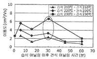
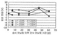
6A is a graph showing the thermal annealing temperature dependency of the mobility of the thin film transistor device according to the embodiment.
6B is a graph showing the thermal annealing temperature dependence of the hysteresis of the thin film transistor device according to the embodiment.
6C is a graph showing the thermal annealing temperature dependency of the turn-on voltage of the thin film transistor device according to the embodiment.
7A is a graph showing the mobility of the thin film transistor device and the gate voltage dependency of the drain current according to the embodiment.
7B is a graph showing the mobility of the thin film transistor device and the gate voltage dependency of the drain current according to the embodiment.
7C is a graph showing the mobility and the gate voltage dependency of the drain current of the thin film transistor device according to the embodiment.
7D is a graph showing the mobility and the gate voltage dependency of the drain current of the thin film transistor device according to the embodiment.
8 is a graph showing the time change with respect to the thermal annealing temperature in the sol-gel reaction according to the embodiment.
9A is a graph showing the mobility of the thin film transistor device according to the embodiment and the gate voltage dependence of the drain current.
9B is a graph showing the mobility of the thin film transistor device according to the embodiment and the gate voltage dependency of the drain current.
9C is a graph showing the mobility of the thin film transistor device according to the embodiment and the gate voltage dependency of the drain current.
9D is a graph showing the mobility of the thin film transistor device according to the embodiment and the gate voltage dependency of the drain current.
9E is a graph showing the mobility of the thin film transistor device according to the embodiment and the gate voltage dependence of the drain current.
9F is a graph showing the mobility of the thin film transistor device according to the embodiment and the gate voltage dependence of the drain current.
10 is a graph showing the time variation with respect to the thermal annealing temperature in the sol-gel reaction according to the embodiment.
11A is a graph showing the mobility and the gate voltage dependence of the drain current of the thin film transistor device according to the embodiment.
11B is a graph showing the mobility of the thin film transistor device according to the embodiment and the gate voltage dependency of the drain current.
11C is a graph showing the mobility of the thin film transistor device according to the embodiment and the gate voltage dependency of the drain current.
11D is a graph showing the mobility of the thin film transistor device according to the embodiment and the gate voltage dependence of the drain current.
11E is a graph showing the mobility of the thin film transistor device according to the embodiment and the gate voltage dependency of the drain current.
12 is a graph showing the time variation with respect to the thermal annealing temperature in the sol-gel reaction according to the embodiment.
13A is a graph showing the dry annealing time dependency of the mobility of the thin film transistor device according to the embodiment.
13B is a graph showing dry annealing time dependency of the hysteresis of the thin film transistor device according to the embodiment.
13C is a graph showing the dry annealing time dependency of the turn-on voltage of the thin film transistor device according to the embodiment.
14A is a graph showing the mobility of the thin film transistor device and the gate voltage dependence of the drain current according to the embodiment.
14B is a graph showing the mobility of the thin film transistor device according to the embodiment and the gate voltage dependency of the drain current.
14C is a graph showing the mobility of the thin film transistor device and the gate voltage dependence of the drain current according to the embodiment.
15 is a graph showing the time variation with respect to the thermal annealing temperature in the sol-gel reaction according to the embodiment.
16A is a graph showing the mobility of the thin film transistor device according to the embodiment and the gate voltage dependency of the drain current.
16B is a graph showing the drain voltage dependence of the drain current of the thin film transistor with respect to each of the different gate voltages.
17A is a graph showing the mobility and the gate voltage dependency of the drain current of the thin film transistor device according to the second modification of the present invention.
17B is a graph showing the mobility and the gate voltage dependency of the drain current of the thin film transistor device according to the second modification of the present invention.
17C is a graph showing the mobility and the gate voltage dependency of the drain current of the thin film transistor device according to the second modification of the present invention.
18A is a graph showing the mobility and the gate voltage dependency of the drain current of the thin film transistor device according to the second modification of the present invention.
18B is a graph showing the mobility of the thin film transistor device according to the second modification of the present invention and the gate voltage dependency of the drain current.
19 is a graph showing the mobility and the gate voltage dependency of the drain current of the thin film transistor device according to the second modification of the present invention.
상기 언급된 목적을 달성하기 위해, 본 발명의 한 측면에 따른 금속 산화물 반도체를 제조하는 방법은: 용매 내 적어도 하나는 금속 알콕사이드인 적어도 2개의 전구체들의 혼합 용액으로부터 막을 기판에 증착하는 단계 및 혼합 용액으로부터 금속 산화물 반도체를 형성하기 위해, 수성 촉매가 존재하는 경우에 이를 포함하여 기판상에 증착된 막을 경화하는 단계를 포함한다.According to an aspect of the present invention, there is provided a method for fabricating a metal oxide semiconductor, the method comprising: depositing a film from a mixed solution of at least two precursors in a solvent, the at least one being a metal alkoxide, And curing the deposited film on the substrate, if any, in the presence of an aqueous catalyst to form a metal oxide semiconductor from the substrate.
본 발명의 또 다른 측면에 따른 비정질 금속 산화물 반도체를 제조하는 방법은: 용매 내 하나는 예컨대 인듐 알콕사이드이고, 다른 하나는 예컨대 아연 알콕사이드이며, 반대의 경우도 포함하는 적어도 2개의 전구체들의 혼합 용액으로부터 막을 기판에 증착하는 단계 및 혼합 용액으로부터 비정질 금속 산화물 반도체를 형성하기 위해 수증기 분위기에서 180 내지 275℃의 온도 범위(경계값 포함)에서 기판에 증착된 막을 열 어닐링하는 단계를 포함한다.A process for producing an amorphous metal oxide semiconductor according to another aspect of the present invention comprises: forming a film from a mixed solution of at least two precursors, one in a solvent being, for example, an indium alkoxide and the other being a zinc alkoxide, Annealing the film deposited on the substrate at a temperature in the range of 180 to 275 DEG C (including the boundary value) in a water vapor atmosphere to form an amorphous metal oxide semiconductor from the mixed solution.
상기 측면에서, 막은, 용매 내 적어도 인듐 알콕사이드와 아연 알콕사이드의 혼합 용액으로부터 기판상에 증착된다. 기판은 수증기 분위기에 배치된다. 그러므로 습기가 혼합 용액에서 만들어진 막에 활발하게 주입되면 이 막이 겔로 변한다. 혼합 용액에서 만들어진 막이 겔로 변하는 단계에 있어서, 400℃ 이상의 고온을 사용하여 수증기를 생성해 습기를 막에 주입하는 것 대신, 막이 증착되는 기판이 수증기 분위기에 배치된다. 게다가, 400℃ 이상의 고온을 사용하지 않아도 혼합 용액에서 만들어진 막에 습기를 활발히 주입할 수 있다. 혼합 용액에서 만들어진 막으로 습기가 주입된 이후 열 어닐링 단계가 수행되므로, 400℃ 이상의 고온에서 전구체의 열 분해를 수행할 필요가 없다. 심지어, 180℃ 내지 275℃ 사이의 저온(경계값 포함)으로, 반응 시스템 내의 이탈기(leaving group) 성분은 충분히 제거될 수 있다. 그러므로 혼합 용액에서 만들어진 막에 대한 열 어닐링 온도는 수증기 분위기에서 막이 증착되는 기판을 위치시키는 것에 의해 낮춰질 수 있어서, 혼합 용액에 습기를 활발히 주입하고 혼합 용액에서 만들어진 박막을 겔로 변화시킬 수 있다. 결과적으로, 비정질 금속 산화물 반도체는 플라스틱 기판처럼 비교적 낮은 내열성을 가지는 기판을 사용하여 형성될 수 있다.In this aspect, the film is deposited on a substrate from a mixed solution of at least an indium alkoxide and a zinc alkoxide in a solvent. The substrate is placed in a water vapor atmosphere. Therefore, when the moisture is actively injected into the membrane made in the mixed solution, the membrane becomes gel. In the step of changing the film made in the mixed solution into the gel, instead of generating steam by using a high temperature of 400 DEG C or higher to inject moisture into the film, the substrate on which the film is deposited is placed in a water vapor atmosphere. In addition, moisture can be actively injected into a film made in a mixed solution without using a high temperature of 400 DEG C or higher. It is not necessary to perform the thermal decomposition of the precursor at a high temperature of 400 DEG C or more since the thermal annealing step is performed after the moisture is injected into the film made in the mixed solution. Even at low temperatures (including boundary values) between 180 ° C and 275 ° C, the leaving group components in the reaction system can be sufficiently removed. Therefore, the thermal annealing temperature for the film made in the mixed solution can be lowered by placing the substrate on which the film is deposited in the water vapor atmosphere, so that moisture can be actively injected into the mixed solution and the thin film made in the mixed solution can be converted into gel. As a result, the amorphous metal oxide semiconductor can be formed using a substrate having a relatively low heat resistance, such as a plastic substrate.
예컨대, 열 어닐링 단계는 수증기 분위기에서의 180℃ 내지 275℃의 온도 범위(경계값 포함)에서의 열 어닐링 단계(이하에서 제 1 처리로도 지칭됨); 및 수증기 분위기에서의 열 어닐링 단계 이후 비수증기 분위기에서의 180℃ 내지 275℃의 온도 범위(경계값 포함)에서의 열 어닐링 단계(이하에서 제 2 처리로도 지칭됨)를 포함할 수 있다.For example, the thermal annealing step may include a thermal annealing step (hereinafter also referred to as a first treatment) at a temperature range of 180 DEG C to 275 DEG C (including a boundary value) in a water vapor atmosphere; And a thermal annealing step at a temperature range of 180 ° C to 275 ° C (inclusive of the boundary value) (hereinafter also referred to as a second treatment) in a non-aqueous atmosphere after the thermal annealing step in the water vapor atmosphere.
상기 측면에 있어서, 겔링 단계는 이탈기 성분을 활발하게 제거하기 위하여 열 어닐링 단계에서 분리된다. 먼저, 혼합 용액에서 만들어진 막은 수증기 대기에 배치됨으로써 겔로 변화되고, 그 후 열 어닐링 단계가 수행된다. 그러므로 열 어닐링 단계에서 겔링 단계를 분리함으로써, 혼합 용액에 대한 열 어닐링 온도는 낮춰질 수 있다. 결과적으로, 플라스틱 기판처럼 비교적 낮은 내열성을 가지는 기판을 사용하는 것이 가능하다.In this aspect, the gelling step is separated in the thermal annealing step to actively remove the leaving group components. First, the membrane made in the mixed solution is converted into a gel by being placed in a water vapor atmosphere, and then a thermal annealing step is performed. Therefore, by separating the gelling step in the thermal annealing step, the thermal annealing temperature for the mixed solution can be lowered. As a result, it is possible to use a substrate having a relatively low heat resistance such as a plastic substrate.
예컨대, 비수증기 분위기에서의 열 어닐링 단계(제 2 처리)는 수증기 분위기에서의 열 어닐링 단계(제 1 처리)가 완료된 후에 연속해서 수행될 수 있다.For example, the thermal annealing step (second treatment) in a non-aqueous steam atmosphere can be performed continuously after the thermal annealing step (first treatment) in the steam atmosphere is completed.
상기 측면에 따르면, 제 1 처리 및 제 2 처리를 연달아 수행함으로써, 금속 산화물의 메쉬 구조는 충분한 산소를 공급하는 동안 비수증기 분위기에서 이탈기 성분을 제거함으로써 양호하게 형성될 수 있어서 적은 양의 잔여 불순물 및 산소 결함을 갖는 비정질 금속 산화물 반도체를 형성하는 것이 가능하다. 결과적으로, 비정질 금속 산화물의 반도체성을 크게 개선하고 안정화하는 것이 가능하다.According to this aspect, by performing the first treatment and the second treatment sequentially, the mesh structure of the metal oxide can be preferably formed by removing the leaving component in a non-aqueous atmosphere while supplying sufficient oxygen, so that a small amount of residual impurities And an amorphous metal oxide semiconductor having oxygen defects can be formed. As a result, it is possible to significantly improve and stabilize the semiconducting property of the amorphous metal oxide.
예컨대, 수증기 분위기에서의 열 어닐링 단계(제 1 처리) 및 비수증기 분위기에서의 열 어닐링 단계(제 2 처리)는 동일한 온도에서 수행될 수 있다.For example, the thermal annealing step (first treatment) in a steam atmosphere and the thermal annealing step (second treatment) in a non-steam atmosphere can be performed at the same temperature.
상기 측면에 따라, 열 어닐링 온도가 제 1 처리와 제 2 처리 사이에서 동일해지므로 처리가 간소화될 수 있다.According to this aspect, the thermal annealing temperature is the same between the first process and the second process, so that the process can be simplified.
예컨대, 금속 전구체들 중 하나는 제 1 온도 범위 내에 속하는 분해 온도(decomposition temperature)를 갖는 인듐 알콕사이드가 될 수 있으며, 제 2 전구체는 제 2 온도 범위 내에 속하는 분해 온도를 갖는 아연 알콕사이드가 될 수 있고, 제 2 온도는 제 1 온도 범위와 중첩된다.For example, one of the metal precursors may be an indium alkoxide having a decomposition temperature falling within a first temperature range, the second precursor may be a zinc alkoxide having a decomposition temperature falling within a second temperature range, The second temperature overlaps the first temperature range.
상기 측면에 따라, 인듐 알콕사이드의 분해 온도의 온도 범위와 아연 알콕사이드의 분해 온도의 온도 범위는 중첩된다. 따라서, 인듐 및 아연이 동시에 분해되므로, 두 금속 성분의 본딩(bonding)은 더욱 효과적으로 촉진된다. 결과적으로, 비정질 상태는 안정적으로 형성될 수 있으며 최종 산물로서 비정질 금속 산화물 반도체를 안정적으로 형성하는 것이 가능하다.According to this aspect, the temperature range of the decomposition temperature of the indium alkoxide and the decomposition temperature of the zinc alkoxide are overlapped. Therefore, since indium and zinc are decomposed at the same time, the bonding of the two metal components is more effectively promoted. As a result, the amorphous state can be stably formed, and it is possible to stably form an amorphous metal oxide semiconductor as a final product.
상기 측면에 따라, 인듐 알콕사이드는 예컨대 팬타메릭 인듐 알콕사이드 클러스터를 포함하고, 아연 알콕사이드는 예컨대 아연 비스 메톡시에톡사이드를 포함하며, 기판에 증착된 막은 210℃ 내지 275℃의 온도 범위(경계값 포함)에서 수증기 분위기에서 열 어닐링된다.According to this aspect, the indium alkoxide includes, for example, a pantameric indium alkoxide cluster, the zinc alkoxide includes, for example, zinc bismethoxyethoxide, and the film deposited on the substrate has a temperature in the range of 210 DEG C to 275 DEG C Lt; / RTI > in a steam atmosphere.
상기 측면에 따라, 인듐 알콕사이드는 예컨대 팬타메릭 인듐 알콕사이드 클러스터를 포함하고, 아연 알콕사이드는 예컨대 알킬 성분, 아릴 성분, 퍼플루오르아릴 성분, 퍼플루오르알킬 성분 또는 플루오르탄화수소 성분을 포함할 수 있다.According to this aspect, the indium alkoxide includes, for example, a pantameric indium alkoxide cluster, and the zinc alkoxide may include, for example, an alkyl component, an aryl component, a perfluoroaryl component, a perfluoroalkyl component, or a fluorohydrocarbon component.
상기 측면에 따라, 아연 알콕사이드는 예컨대 에틸징크 프로폭사이드, 에틸징크 부톡사이드 또는 에틸징크 메톡시에톡사이드를 포함한다.According to this aspect, the zinc alkoxide includes, for example, ethyl zinc propoxide, ethyl zinc butoxide or ethyl zinc methoxyethoxide.
상기 측면에 따라, 혼합 용액은, 예컨대 I, II or III족 금속 알콕사이드 전구체에 포함된 다른 금속 알콕사이드 전구체들을 추가로 포함한다.According to this aspect, the mixed solution further comprises other metal alkoxide precursors included, for example, in the I, II or Group III metal alkoxide precursors.
상기 측면에 따라, 다른 금속 알콕사이드 전구체는 예컨대 갈륨, 바륨 또는 스트론튬을 포함한다.According to this aspect, the other metal alkoxide precursor includes, for example, gallium, barium or strontium.
본 발명의 발명자들은 금속 알콕사이드를 출발 물질로 사용하고 졸겔 반응을 사용하여 비정질 금속 산화물 반도체를 최종 산물로서 형성하고자 한다. 본 발명의 발명자들은 가수분해 반응을 나타내는 이하의 식 1에서의 물의 역할과 축중합 반응을 나타내는 식 2 또는 식 3에 초점을 맞추었다. 졸겔 반응에서, 금속 알콕사이드의 가수분해 반응은 추가된 물의 양에 비례하여 진행되어서, 식 1의 공통식 M(OR)x-y(OH)에 의해 제시되는 중간 산물이 생성된다. 식 2 또는 식 3에 의해 제시되는 축중합 반응은 생성된 중간 산물의 양에 비례하여 진행되어서, 비정질 금속 산화물 반도체를 생성한다. 그러므로 충분한 물이 공급되는 환경에서, 비교적 저온에서 열 어닐링 단계를 이용하여 졸겔 반응을 촉진하는 것이 가능하다. 식 1에서 식 3까지, M은 금속을, OR은 알킬기를 의미한다는 점이 주목된다.The inventors of the present invention intend to form amorphous metal oxide semiconductors as final products by using a metal alkoxide as a starting material and using a sol-gel reaction. The inventors of the present invention focused on the role of water in the following
M(OR)x+yH2O→M(OR)x-y(OH)+(x-y)H-OR(식 1)M (OR) x + yH 2 O → M (OR) xy (OH) + (xy) H-OR ( formula 1)
(RO)2M-OH+HO-M(OR)2→M-O-M+H2O(식 2)(RO) 2 M-OH + HO-M (OR) 2 → MO-M + H 2 O ( Equation 2)
(RO)2M-OH+RO-M(OR)2→M-O-M+R-OH(식 3)(RO)2 M-OH + RO-M (OR)2 - ???????? MO-M +
충분한 물을 공급받는 환경에서, 열 어닐링 단계는 온도를 이용하여 수행될 수 있고, 이 온도는 공통식 RH-O에 의해 제시되고 졸겔 반응의 부산물인 (i) 유기 물질 또는 (ii) H2O를 분산시키기(반응 시스템 이내의 이탈기를 제거해 반응의 균형을 산물의 측면에 바이어스 하여)에 충분하다. 이 온도는, 또한, 오로지 가열만을 사용하는 전구체의 열 분해에서의 온도에 비해 상당히 낮다. 본 발명의 발명자들은 물 추가 없이 용액의 유동성이 유지된 채로 기판에 금속 알콕사이드 용액을 출발물질로서 증착함으로써 박막을 쉽게 증착하고 형성하는 것에 이르렀다. 이후 금속 알콕사이드의 졸겔 반응은 그 뒤에 노출에 의해 촉진되고, 이 금속 알콕사이드 용액은 수증기 분위기에서 기판에 적층되고, 비정질 금속 산화물 반도체는 낮은 온도에서 얻어진다. 상기 설명대로, 본 발명의 발명자들은 본 발명에 이르렀다.In an environment where sufficient water is supplied, the thermal annealing step can be carried out using temperature, which is a byproduct of the sol-gel reaction, represented by the common formula RH-O, (i) organic material or (ii) H2 O (By removing the leaving group within the reaction system to bias the reaction to the side of the product). This temperature is also significantly lower than the temperature in the thermal decomposition of the precursor using only heating. The inventors of the present invention have succeeded in easily depositing and forming a thin film by depositing a metal alkoxide solution as a starting material on a substrate while maintaining the fluidity of the solution without adding water. The sol-gel reaction of the metal alkoxide is then promoted by exposure, and the metal alkoxide solution is deposited on the substrate in a water vapor atmosphere, and the amorphous metal oxide semiconductor is obtained at low temperatures. As described above, the inventors of the present invention have reached the present invention.
이것으로, 본 발명은 용매 내 적어도 인듐 알콕사이드 및 아연 알콕사이드의 혼합 용액을 출발 물질로 사용함으로써 우수한 막 성질을 가진 비정질 금속 산화물 반도체를 최종 산물로서 형성하고, 증착에 의해 기판에 박막을 형성한 후 수증기 분위기에서 210℃와 275℃ 사이의 온도(경계값 포함)로 중간 처리로서 열 어닐링 단계를 수행하는 것에 성공한다.Accordingly, the present invention provides an amorphous metal oxide semiconductor having excellent film properties as a final product by using a mixed solution of at least indium alkoxide and zinc alkoxide in a solvent as a starting material, forming a thin film on the substrate by vapor deposition, Lt; RTI ID = 0.0 > 210 C < / RTI > and 275 C (including boundary values) in the atmosphere.
예컨대, 중간 처리는 제 1 처리 및 제 2 처리로 나뉠 수 있다. 열 어닐링 단계는 제 1 처리에서 수증기 분위기에서의 210℃와 275℃ 사이의 온도(경계값 포함)로 수행되며, 열 어닐링 단계는 제 2 처리에서 비수증기 분위기에서의 210℃와 275℃ 사이의 온도(경계값 포함)로 수행된다.For example, the intermediate processing may be divided into a first processing and a second processing. The thermal annealing step is carried out at a temperature between 210 [deg.] C and 275 [deg.] C in the water vapor atmosphere in the first treatment (inclusive) and the thermal annealing step is carried out at a temperature between 210 [deg.] C and 275 [ (Including boundary values).
이러한 특성은 다음과 같다:These characteristics are as follows:
(1) 수증기 분위기에서의 210℃와 275℃ 사이의 온도(경계값 포함)로 열 어닐링 단계를 수행; 및(1) performing a thermal annealing step at a temperature between 210 < 0 > C and 275 < 0 > C (including a boundary value) in a water vapor atmosphere; And
(2) 수증기 분위기에서의 제 1 처리 및 비수증기 분위기에서의 제 2 처리 양방을 결합하고, 제 1 처리 및 제 2 처리를 연이어 수행.(2) Combining both the first treatment in a steam atmosphere and the second treatment in a non-steam atmosphere, followed by the first treatment and the second treatment successively.
특성(1)에 따라, 물은 용매에서의 인듐 알콕사이드 및 아연 알콕사이드의 혼합 용액으로부터 만들어진 박막에 활발히 공급된다. 이것으로, 박막은 겔로 변화하고 열 어닐링 단계는 물이 활발히 공급된 상태에서 연이어 수행된다.According to characteristic (1), water is actively supplied to a thin film made from a mixed solution of indium alkoxide and zinc alkoxide in a solvent. With this, the thin film changes to gel and the thermal annealing step is carried out successively with water being actively supplied.
이러한 점에 있어서, 종래에는, 용매 내 인듐 알콕사이드 및 아연 알콕사이드의 혼합 용액으로부터 만들어진 박막은 400℃의 고온에서 열 어닐링되며 전구체의 분해는 주로 열 분해에 의해 촉진되어서 박막을 겔로 변화시킨다. 다시 말해서, 이탈기를 활발히 제거하기 위한 겔링 단계 및 열 어닐링 단계 양방은 고온을 활용함으로써 수행된다.In this regard, conventionally, a thin film made from a mixed solution of indium alkoxide and zinc alkoxide in a solvent is thermally annealed at a high temperature of 400 DEG C, and decomposition of the precursor is mainly promoted by thermal decomposition, thereby changing the thin film to gel. In other words, both the gelling step and the thermal annealing step for actively removing the leaving group are performed by utilizing the high temperature.
반대로, 본 발명에서는, 혼합 용액에서 만들어진 막이 증착된 기판이 수증기 분위기에 위치되므로, 습기를 혼합 용액에 활발히 주입하여 혼합 용액에서 만들어진 박막을 겔로 변화시킨다.In contrast, in the present invention, since the substrate on which the film made of the mixed solution is deposited is placed in the water vapor atmosphere, moisture is actively injected into the mixed solution to change the thin film made of the mixed solution into gel.
이 시점에서, 400℃ 이상 고온에서의 열 어닐링 처리에서 수증기를 생성하고 이러한 수증기를 통해 혼합 용액에서 만들어진 박막을 겔로 변화시키는 대신, 혼합 용액에서 만들어진 막이 증착되는 기판을 수증기 분위기에 위치시켜서 습기가 혼합 용액에 활발히 주입된다. 열 어닐링 단계가 습기가 활발히 주입되는 상태에서 수행되므로, 400℃ 이상 고온에서의 전구체의 열 분해를 수행할 필요가 없다. 이처럼, 겔링 단계는 210℃와 275℃ 사이의 저온(경계값 포함)으로도 충분히 진행될 수 있다. 혼합 용액을 위한 열 어닐링 온도는 혼합 용액으로부터 만들어지는 막이 증착되는 기판을 수증기 분위기에 위치시킴으로써 낮춰질 수 있어서, 혼합 용액에 습기를 활발히 주입하고 혼합 용액으로부터 만들어진 박막을 겔로 변화시킨다.At this point, instead of changing the thin film made in the mixed solution into gel by generating steam in the thermal annealing treatment at a temperature higher than 400 DEG C and placing the substrate on which the film made from the mixed solution is deposited in the steam atmosphere through the water vapor, It is actively injected into the solution. Since the thermal annealing step is carried out in a state where moisture is actively injected, it is not necessary to perform the thermal decomposition of the precursor at a temperature higher than 400 캜. As such, the gelling step can proceed well at low temperatures (including boundary values) between 210 캜 and 275 캜. The thermal annealing temperature for the mixed solution can be lowered by placing the substrate on which the film made from the mixed solution is deposited in a steam atmosphere, actively injecting moisture into the mixed solution and changing the thin film made from the mixed solution into gel.
게다가, 본 발명의 실시예에서, 겔링 단계는 이탈기 성분을 활발히 제거하기 위하여 열 어닐링 단계에서 분리된다. 다시 말해, 먼저, 혼합 용액으로부터 만들어진 박막은 수증기 분위기에 박막을 위치시킴으로써 겔로 변화하고 그 후 열 어닐링 단계가 수행된다. 이처럼, 210℃ 내지 275℃ 사이의 저온(경계값 포함)으로도, 반응 시스템 내의 이탈기 성분은 충분히 제거될 수 있다. 다시 말해서, 열 어닐링 단계에서 겔링 단계를 분리함으로써, 혼합 용액을 위한 열 어닐링 온도는 낮춰질 수 있다.In addition, in an embodiment of the present invention, the gelling step is separated in the thermal annealing step to actively remove the leaving group component. In other words, first, a thin film made from a mixed solution is converted into a gel by placing the thin film in a water vapor atmosphere, and then a thermal annealing step is performed. As such, even at low temperatures (including boundary values) between 210 ° C and 275 ° C, the leaving group components in the reaction system can be sufficiently removed. In other words, by separating the gelling step in the thermal annealing step, the thermal annealing temperature for the mixed solution can be lowered.
게다가, 특성(2)에 따르면, 제 1 처리 및 제 2 처리를 연이어 수행함으로써, 충분한 산소를 공급하는 동안 비 수증기 분위기에서 이탈기 성분을 제거함으로써 금속 산화물의 메쉬 구조는 충분히 형성되어서, 극소량의 잔여 불순물 및 산소 결함을 가지는 비정질 금속 산화물 반도체를 형성하는 것이 가능하다. 결과적으로 이동도, 히스테리시스 등과 같은 반도체성을 크게 개선하고 안정화하는 것 또한 가능하다.Further, according to the characteristic (2), by performing the first treatment and the second treatment successively, the mesh structure of the metal oxide is sufficiently formed by removing the leaving component in the non-aqueous atmosphere while supplying sufficient oxygen, It is possible to form an amorphous metal oxide semiconductor having impurities and oxygen defects. As a result, it is also possible to largely improve and stabilize semiconducting properties such as mobility, hysteresis and the like.
이후에서, 본 발명의 실시예의 비정질 금속 산화물 반도체를 제조하는 방법이 도면을 참조하여 기재될 것이다. 후속 도면에서, 기재를 간소화하기 위해, 사실상 동일한 기능을 가지는 구성 요소들에는 동일한 참조 부호가 주어진다.Hereinafter, a method of manufacturing an amorphous metal oxide semiconductor of an embodiment of the present invention will be described with reference to the drawings. In the following figures, to simplify the description, elements having substantially the same function are given the same reference numerals.
도 1은 본 발명의 실시예에 따른 박막 트랜지스터 디바이스를 제조하기 위한 방법을 도식적으로 설명하는 단면도이다.1 is a cross-sectional view schematically illustrating a method for manufacturing a thin film transistor device according to an embodiment of the present invention.
먼저, 도 1의 (a)에서 도시된 바에 따르면, 예컨대 실리카 글라스, 플라스틱 등으로부터 만들어진 기판(10)이 준비된다.First, as shown in Fig. 1 (a), a
다음으로, 도 1의 (b)에 도시된 바에 따르면, 게이트 전극(11)이 기판(10)에 형성된다. 예컨대, 몰리브덴 텅스텐(MoW) 및 이와 유사한 것과 같은 금속으로부터 만들어진 금속 막이 스퍼터링 및 이와 유사한 것에 의해 기판(10)상에 형성된 이후, (도시되지 않은) 포토레지스트 마스크를 사용하는 습식 에칭이 수행되며 이 금속 막은 미리 결정된 형상으로 패터닝된다. 패터닝이 수행되는 금속 막이 게이트 전극(11)으로서 형성된다.Next, as shown in Fig. 1 (b), a
다음으로, 도 1의 (c)에 도시된 바에 따르면, 실리콘 산화물(SiOx), 실리콘 질화물(SiNy), 이것들의 적층된 층들 등으로부터 만들어지는 게이트 절연막(12)이 게이트 전극(11)에 형성된다.Next, as shown in Fig. 1 (c), a
다음으로, 도 1의(d)에 도시된 바에 따르면, 비정질 금속 산화물 반도체 층(13)은 졸겔 방법을 사용하여 채널 층으로서 게이트 절연막(12)에 형성된다. 비정질 금속 산화물 반도체 층(13)을 형성하는 방법은 이후에서 상세하게 기재된다.Next, as shown in FIG. 1 (d), the amorphous metal
다음으로, 도 1의 (e)에 도시된 바에 따르면, 포토레지스트 마스크 등을 사용하는 습식 에칭은 비정질 금속 산화물 반도체 층(13)에 수행되며, 비정질 금속 산화물 반도체 층(13)은 미리 결정된 형상으로 패터닝된다.Next, as shown in FIG. 1 (e), wet etching using a photoresist mask or the like is performed on the amorphous metal
다음으로, 도 1의 (f)에 도시된 바에 따르면, 소스 전극(14) 및 드레인 전극(15)은 채널 방향으로 스퍼터링 등에 의해 비정질 금속 산화물 반도체 층(13)의 반대쪽 단부에 각각 이격되어 형성된다. 각각의 소스 전극(14) 및 드레인 전극(15)는 단층 구조 또는 전도성 물질, 합금(alloy) 등의 다층 구조이며, 예컨대 알루미늄(Al), 몰리브덴(Mo), 텅스텐(W), 구리(Cu), 몰리브덴 텅스텐(MoW), 티타늄(Ti), 크롬(Cr) 등을 포함한다.1 (f), the
마지막으로, 도 1의 (g)에 도시된 바에 따라, 패시베이션 막(16)이 형성되어 박막 트랜지스터 디바이스의 전체를 커버한다.Finally, as shown in Fig. 1 (g), a
도 2는 박막 트랜지스터 디바이스를 제조하는 상기 기재된 방법의 비정질 금속 산화물 반도체 층(13)을 형성하는 처리(도 1의 (d)에 도시된 처리)의 세부사항을 도시하는 단면도이다.Fig. 2 is a cross-sectional view showing the details of the process (the process shown in Fig. 1 (d)) of forming the amorphous metal
먼저, 도 2의 (a)에서 도시된 바에 따르면, 적어도 인듐 알콕사이드 및 아연 알콕사이드를 포함하는 혼합 용액 역할을 하는 금속 알콕사이드 용액(20)이 기판(10)(특히, 게이트 절연막(12)에)에 증착된다.2 (a), a
다음으로, 도 2의 (b)에 도시된 바에 따르면, 열 어닐링 단계는 210℃ 내지 275℃ 사이의 온도 범위(경계값 포함)에서 수증기 분위기에서 기판(10)상에 증착되는 금속 알콕사이드 용액(20)에 수행되며, 졸겔 반응의 가수분해 반응은 습기를 금속 알콕사이드 용액(20) 내에 활발히 주입하여 촉진된다. 이것으로, 가수분해된 박막(21)이 형성된다. 게다가, 도 2의 (c)에 도시된 대로, 수증기 분위기에서의 210℃와 275℃ 사이의 온도(경계값 포함)로 열 어닐링 단계를 지속함으로써, 졸겔 반응의 축중합 반응이 진행되고 축중합되고 겔링된 박막(22)이 형성된다.Next, as shown in FIG. 2 (b), the thermal annealing step is performed to remove the metal alkoxide solution 20 (FIG. 2 (b)) deposited on the
여기서, "수증기 분위기에서"는 습기가 금속 알콕사이드 용액(20)에 활발히 더해지는(주입되는) 상태를 지칭하며, 예컨대, 비정질 금속 산화물 반도체 층의 형성 처리가 수행되는 분위기의 습도보다 더 높은 습도를 의미한다. 이러한 상태는 비정질 금속 산화물 반도체 층(13)이 형성되는 용기의 습도를 지속적으로 제어하여 분위기의 습도보다 더 높아지도록, 즉, 예컨대 습도를 100%까지 증가시킴으로써 실현되거나, 또는 기판(10)에 증착되는 금속 알콕사이드 용액(20)에 수증기를 분사함으로써 실현된다.Refers to a state in which moisture is actively added (injected) to the
다음으로, 도 2의 (d)에 도시된 바에 따르면, 도 2의 (b)와 (c)에서의 처리 이후 잇따라서 비수증기 분위기에서 210℃ 내지 275℃ 사이의 온도(경계값 포함)로 겔링된 박막(21)(기판(10)에 증착되는 금속 알콕사이드 용액(20))에 열 어닐링이 수행된다. 이것으로, 유기 화합물, H20등과 같은 이탈기 성분이 활발히 제거되어 축중합 반응 또한 촉진되어서, 비정질 금속 산화물 반도체 층(13)은 졸겔 반응의 최종 산물로서 혼합 용액으로부터 생성된다.Next, as shown in Fig. 2 (d), after the processing in Figs. 2 (b) and 2 (c), the gelling is performed at a temperature of between 210 [deg.] C and 275 [deg.] C The annealed thin film 21 (
여기서, "비수증기 분위기에서"는 습기가 금속 알콕사이드 용액(20)에 활발히 더해지지 않은 상태를 지칭하며, 예컨대, 비정질 금속 산화물 반도체 층의 형성 처리가 수행되는 분위기의 습도를 의미한다. 이러한 상태는 비정질 금속 산화물 반도체 층(13)의 형성이 수행되는 용기의 습도를 지속적으로 제어하여 분위기의 습도와 동일해짐에 따라 실현되거나 공기에서 기판(10)에 증착되는 금속 알콕사이드 용액(20)에 열 어닐링을 수행함으로써 실현된다.Here, "in a non-aqueous vapor atmosphere" refers to a state in which moisture is not actively added to the
졸겔 반응의 가수분해 반응 및 축중합 반응은 도 2의 (b) 및 도 2의 (c)에서 도시된, 상이한 처리로 분리됨으로써 도시된다는 것이 주목된다. 그러나 가수분해 반응 및 축중합 반응이 졸겔 반응에서 연속적으로 진행되므로, 도 2의 (b) 및 도 2의 (c)의 처리는 수증기 분위기에서 210℃와 275℃ 사이의 온도(경계값 포함)로, 기판(10)에 증착된 금속 알콕사이드 용액(20)에 열 어닐링을 수행하는 단일 처리에서 통합될 수 있다.It is noted that the hydrolysis reaction and the polycondensation reaction of the sol-gel reaction are shown by separating into different treatments shown in Figs. 2 (b) and 2 (c). However, since the hydrolysis reaction and the condensation polymerization reaction proceed continuously in the sol-gel reaction, the treatments of FIGS. 2 (b) and 2 (c) are carried out in a steam atmosphere at a temperature between 210 ° C. and 275 ° C. , In a single process that performs thermal annealing to the
더욱이, 도 2의 (b) 및 도 2의 (c)에서 도시된 처리에서, 210℃와 275℃의 온도 범위(경계값 포함)에서의 열 어닐링에 의해 비정질 금속 산화물 반도체 층(13)이 최종 산물로서 생성되는 경우, 도 2의 (d)에서 도시된 비수증기 분위기에서의 열 어닐링의 처리는 수행될 필요가 없다. 그러므로 이하에서, 열 어닐링이 단독으로 언급될 경우, 이것은 도 2의 (b)와 도 2의 (c)에 도시된 수증기 분위기에서의 열 어닐링(이후 습식 어닐링으로 표시됨)과 도 2의 (d)에 도시된 비수증기 분위기에서의 열 어닐링(이후에서 건식 어닐링으로 표시됨)의 구분없이, 금속 알콕사이드 용액(20)으로부터 비정질 금속 산화물 반도체 층(10)을 얻기 위한 열 어닐링을 뜻하는 것이다.2B and 2C, the amorphous metal
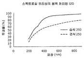
도 3a는 박막 트랜지스터 디바이스의 비정질 금속 산화물 반도체 층의 이차이온질량분석기(SIMS)에 의해 얻어지는 깊이 방향(두께 방향)으로의 탄소(C)와 수소(H)의 농도 분포를 도시하는 그래프이다. 도 3b는 비정질 금속 산화물 반도체 층의 투과율의 파장 의존성을 도시하는 그래프이다.3A is a graph showing concentration distributions of carbon (C) and hydrogen (H) in a depth direction (thickness direction) obtained by a secondary ion mass spectrometer (SIMS) of an amorphous metal oxide semiconductor layer of a thin film transistor device. 3B is a graph showing the wavelength dependency of the transmittance of the amorphous metal oxide semiconductor layer.
도 3a 및 도 3b에서, 실선은 본 실시예에 따라 250℃의 열 어닐링 온도에서 도 1의 (a) 내지 (g)의 방법에 따라 제조되는 박막 트랜지스터 디바이스에서의 농도 분포를 뜻하며, 점선은 250℃의 열 어닐링 온도에서의 종래의 박막 트랜지스터 디바이스의 농도 분포를 뜻한다는 점이 주목된다. 3A and 3B, the solid line represents the concentration distribution in the thin film transistor device manufactured according to the method of FIGS. 1 (a) to (g) at a thermal annealing temperature of 250 DEG C according to the present embodiment, Quot; refers to the concentration distribution of a conventional thin film transistor device at a thermal annealing temperature of < RTI ID = 0.0 > 200 C. < / RTI >
더욱이, 도 3a에서, 수평축인 시간은 비정질 금속 산화물 반도체 층의 깊이에 해당하므로, 0분은 비정질 금속 산화물 반도체 층의 표면을 뜻하고 300분은 게이트 절연막을 가지는 계면(interface)을 뜻한다.3A, the horizontal axis corresponds to the depth of the amorphous metal oxide semiconductor layer, so 0 min means the surface of the amorphous metal oxide semiconductor layer and 300 min means the interface having the gate insulating film.
종래의 비정질 금속 산화물 반도체 층에 비해, 본 실시예에 따른 비정질 금속 산화물 반도체 층에서, 게이트 절연막과의 계면에서의 탄소 농도는 낮으며 불순물 농도도 낮다는 것을 도 3a를 통해 확인할 수 있다. 더욱이, 종래의 비정질 금속 산화물 반도체 층에 비해, 본 실시예에 따른 비정질 금속 산화물 반도체 층에서, 투과율이 전체적으로 높아서 불순물 농도가 낮다는 것을 도 3b를 통해 확인할 수 있다. 그러므로 본 실시예에 따른 비정질 금속 산화물 반도체 층이 높은 온(on) 전류를 실현할 수 있는 구성을 구비한다는 점을 확인할 수 있다.It can be seen from FIG. 3A that the carbon concentration at the interface with the gate insulating film is low and the impurity concentration is low in the amorphous metal oxide semiconductor layer according to the present embodiment as compared with the conventional amorphous metal oxide semiconductor layer. Further, it can be confirmed from FIG. 3B that the transmittance of the amorphous metal oxide semiconductor layer according to the present embodiment is higher than that of the conventional amorphous metal oxide semiconductor layer, so that the impurity concentration is low. Therefore, it can be seen that the amorphous metal oxide semiconductor layer according to the present embodiment has a structure capable of realizing a high on current.
도 3c는, 금속 알콕사이드 용액(20)에 포함된 인듐 알콕사이드 용액의 분해 온도를 유도하기 위해, 10℃/분의 시간 변화를 뜻하는 퍼니스(furnace) 내 인듐 알콕사이드 용액의 5mg에서 생성되는 가스의 질량에 대한 상대 시간 변화를 도시하는 그래프이다. 도 3d는, 금속 알콕사이드 용액(20)에 포함된 아연 알콕사이드 용액의 분해 온도를 유도하기 위해, 10℃/분의 시간 변화를 뜻하는 퍼니스 내 아연 알콕사이드 용액의 5mg에서 생성되는 가스의 질량에 대한 상대 시간 변화를 도시하는 그래프이다.3C shows the mass of the gas produced in 5 mg of the indium alkoxide solution in the furnace, which means a time change of 10 DEG C / min, to induce the decomposition temperature of the indium alkoxide solution contained in the
금속 알콕사이드 용액(20)에 포함된 인듐 알콕사이드 용액으로, 인듐 알콕사이드 용액이 분해될 경우 생성되는 가스가 190℃와 325℃ 사이의 온도(경계값 포함)에서 생성되어서, 인듐 알콕사이드 용액은 190℃ 내지 325℃의 분해 온도 범위(경계값 포함)를 구비한 인듐 알콕사이드의 무수 알콜 용액이라는 것을 도 3c 통해 확인할 수 있다. 더욱이, 금속 알콕사이드 용액(20)에 포함된 아연 알콕사이드 용액으로, 아연 알콕사이드 용액이 분해될 경우 생성되는 가스가 190℃와 325℃ 사이의 온도(경계값 포함)에서 생성되어서, 아연 알콕사이드 용액은 제 1 온도 범위와 중첩되는 190℃ 내지 325℃의 분해 온도 범위(경계값 포함)(제 2 온도 범위)를 구비한 아연 알콕사이드의 무수 알콜 용액이라는 것을 도 3c 통해 확인할 수 있다. 그러므로 인듐 알콕사이드 용액 및 아연 알콕사이드 용액이 유사한 반응성을 갖고 거의 동시시에 분해되고, 인듐과 아연 사이의 본딩은 졸겔 반응으로 촉진된다는 것을 추론할 수 있다.With the indium alkoxide solution contained in the
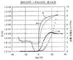
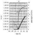
이하에서, 도 1의 방법에 따라 제조되는 본 실시예에 따른 박막 트랜지스터 디바이스의 특성에 대한 평가 결과는 도 4a 및 도 4b, 도 5a 내지 도 5f, 도 6a 내지 도6c, 도 7a 내지 도 7d, 도 9a 내지 도 9f, 도 11a 내지 도 11e, 도 13a 내지 도 13c 및 도 14a 내지 도 14c에 도시된다. 더욱이, 도 4c 내지 도 4e는, 비수증기성 분위기에서 고온으로 졸겔 반응을 촉진시켜서 비정질 금속 산화물 반도체 층이 형성되는 경우에 대한 비교예의 역할을 하는 박막 트랜지스터 디바이스의 특성에 대한 평가 결과를 도시한다.Hereinafter, the evaluation results of the characteristics of the thin film transistor device according to the present embodiment, which is manufactured in accordance with the method of FIG. 1, are shown in FIGS. 4A and 4B, 5A to 5F, 6A to 6C, 7A to 7D, 9A to 9F, 11A to 11E, 13A to 13C, and 14A to 14C. 4C to 4E show evaluation results of the characteristics of the thin film transistor device serving as a comparative example in the case where the amorphous metal oxide semiconductor layer is formed by promoting the sol-gel reaction at a high temperature in a non-aqueous vapor atmosphere.
본 실시예의 박막 트랜지스터의 특성은 이동도, 히스테리시스 및 턴온 전압의 파라미터를 사용하여 나타날 수 있다. 이동도는 드레인 전류 (ID)-게이트 전류 (VGS) 특성의 슬로프로부터 추출될 수 있다. 히스테리시스는, 게이트 전압이 음에서 양으로 바뀌는 경우 드레인 전류의 게이트 전압 의존성과 게이트 전압이 양에서 음으로 바뀌는 경우 드레인 전류의 게이트 전압 의존성 양방에서의 10nA 드레인 전류에서 2개의 전압 사이의 차이이다. 더욱이, 턴온 전압은 온 특성의 상승 전압을 나타내며 로그(ID)-VGS의 슬로프가 최대인 게이트 전압으로서 한정된다.The characteristics of the thin film transistor of this embodiment can be shown using parameters of mobility, hysteresis and turn-on voltage. The mobility can be extracted from the slope of the drain current (ID ) -gate current (VGS ) characteristic. Hysteresis is the difference between the gate voltage of the drain current when the gate voltage changes from negative to positive and the difference between the two voltages at the 10 nA drain current both in the gate voltage dependence of the drain current when the gate voltage changes from positive to negative. Furthermore, the turn-on voltage is defined as the gate voltage at which the slope of the log (ID ) -VGS is the maximum indicating the rising voltage of the on characteristic.
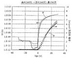
도 4a는 열 어닐링 온도가 275℃로 세팅될 경우 박막 트랜지스터 디바이스의 이동도 및 드레인 전류의 게이트 전압 의존성을 도시하는 그래프이다. 도 4a에서 이동도의 게이트 전압 의존성(도 4a의 A)은 흑백 정사각형("■", "□")으로 도시되며, 드레인 전류의 게이트 전류 의존성(도 4a의 B)은 실선으로 도시된다. 도 4b는 각각의 상이한 게이트 전압에 대한 박막 트랜지스터 디바이스의 드레인 전류의 드레인 전압 의존성을 도시하는 그래프이다.4A is a graph showing the gate voltage dependence of the mobility and drain current of the thin film transistor device when the thermal annealing temperature is set to 275 DEG C. FIG. In FIG. 4A, the gate voltage dependence (A in FIG. 4A) of the mobility is shown in black and white squares ("■", "□") and the gate current dependency of the drain current (FIG. 4B is a graph showing the drain voltage dependence of the drain current of the thin film transistor device for each different gate voltage.
여기서, 도 4a에 따른 박막 트랜지스터 디바이스의 제조에 있어서, 열 어닐링이 수증기 분위기에서 수행되어서 상기 언급된 습식 어닐링이 수행된다. 도 4a에 있어서, 상기 기재된 정의에 기초한 턴온 전압 및 이동도를 추출한 결과, 턴온 전압 Von은 0V며, 최대 이동도는 12.09cm2/Vs임을 주목해야 한다.Here, in the manufacture of the thin film transistor device according to Fig. 4A, thermal annealing is performed in a water vapor atmosphere to perform the above-mentioned wet annealing. In FIG. 4A, the turn-on voltage and mobility based on the above-described definition are extracted and it should be noted that the turn-on voltage Von is 0 V and the maximum mobility is 12.09 cm2 / Vs.
반대로, 도 4c 내지 도 4e는 도 4a 및 도 4b에 대한 비교 예시에 해당하며, 열 어닐링 온도가 275℃, 350℃ 및 450℃에 세팅될 경우 박막 트랜지스터 디바이스의 이동도 및 드레인 전류의 게이트 전압 의존성을 각각 도시하는 그래프이다. 도 4c 내지 도 4e에서, 이동도의 게이트 전압 의존성(도 4a 내지 도 4e의 A)이 흑백 정사각형("■", "□")으로 도시되며, 드레인 전류의 게이트 전압 의존성은 실선으로 도시된다. 여기서, 도 4a의 경우와 달리, 도 4c 내지 도 4e에 따른 박막 트랜지스터 디바이스의 제조 시에, 열 어닐링은 수증기 분위기에서는 수행되지 않아서, 건식 어닐링이 수행된다. 이때, 건식 어닐링 시간은 2시간이다.4C to 4E correspond to comparative examples of FIGS. 4A and 4B. When the thermal annealing temperature is set to 275 DEG C, 350 DEG C and 450 DEG C, the mobility of the thin film transistor device and the gate voltage dependence of the drain current Respectively. In FIGS. 4C to 4E, the gate voltage dependence of the mobility (FIGS. 4A to 4E) is shown as black and white squares ("■", "□") and the gate voltage dependence of the drain current is shown by the solid line. Here, unlike the case of FIG. 4A, in manufacturing the thin film transistor device according to FIGS. 4C to 4E, thermal annealing is not performed in a steam atmosphere, and dry annealing is performed. At this time, the dry annealing time is 2 hours.
도 4c 내지 도 4e에 있어서, 상기 기재된 한정에 기초한 턴온 전압 및 이동도 축출의 결과, 도 4c의 박막 트랜지스터 디바이스의 턴온 전압 Von은 -4V이며 최대 이동도는 0.06cm2/Vs이다. 도 4d의 박막 트랜지스터 디바이스에서, 턴온 전압 Von은 -1V이며, 최대 이동도는 1.4cm2/Vs 이다. 도 4e의 박막 트랜지스터 디바이스에서, 턴온 전압 Von은 -12V이며, 최대 이동도는 13.8cm2/Vs이다.In FIGS. 4C-4E, as a result of the turn-on voltage and mobility evolutions based on the above described limitations, the turn-on voltage Von of the thin film transistor device of FIG. 4C is -4 V and the maximum mobility is 0.06 cm2 / Vs. In the thin film transistor device of Figure 4d, it is a turn-on voltage Von is -1V, the maximum mobility is 1.4cm2 / Vs. In the thin film transistor device of FIG. 4E, the turn-on voltage Von is -12 V and the maximum mobility is 13.8 cm2 / Vs.
본 발명에 따른 박막 트랜지스터 디바이스에서, 비정질 실리콘을 사용하는 종래의 박막 트랜지스터 디바이스의 이동도를 능가하는 이동도, 즉, 1cm2/Vs 이상의 이동도는 275℃의 낮은 열 어닐링 온도로 실현한다는 것을 도 4a 및 도 4b를 통해 알 수 있다.In the thin film transistor device according to the present invention, the mobility exceeding the mobility of a conventional thin film transistor device using amorphous silicon, that is, mobility of 1 cm2 / Vs or more is realized at a low thermal annealing temperature of 275 ° C 4a and 4b.
더욱이, 건식 어닐링 처리만을 이용하는 졸겔 방법을 이용하여 제조된 박막트렌지스터 장치(도 4c 내지 도 4e)에 비해, 턴온 전압, 히스테리시스 및 이동도에 관한 양호한 특성은 본 실시예에 따른 박막 트랜지스터 디바이스에서 실현됨을 알 수 있다.Furthermore, compared with the thin film transistor device (Figs. 4C to 4E) manufactured using the sol-gel method using only the dry annealing process, good characteristics regarding the turn-on voltage, hysteresis and mobility are realized in the thin film transistor device according to this embodiment Able to know.
비록 습식 어닐링만이 어닐링 처리로서 수행되고 어닐링 온도는 도 4a 및 도 4b에 따라 본 실시예에서 275℃이지만, 습식 어닐링 온도는 심지어 275℃ 미만의, 예컨대, 230℃가 될 수 있음을 주목해야 한다. 이후에 기재될 도 11a에 도시될 바에 따르면 본 실시예에서, 비정질 실리콘을 사용하는 종래의 박막 트랜지스터에서의 이동도를 능가하는, 즉, 도 4c 내지 도 4e와 비교하여 1cm2/Vs 이상의 이동도가 실현되며 턴온 전압, 히스테리시스 및 이동도에 관한 양호한 특성이 실현된다.It should be noted that although only wet annealing is performed as an annealing process and the annealing temperature is 275 占 폚 in this embodiment according to Figs. 4a and 4b, the wet annealing temperature may even be less than 275 占 폚, e.g., 230 占 폚 . 11A to be described later, in this embodiment, the mobility exceeding the mobility in the conventional thin film transistor using amorphous silicon, that is, the mobility of 1 cm2 / Vs or more as compared with FIGS. 4C to 4E And good characteristics regarding turn-on voltage, hysteresis and mobility are realized.
이처럼, 습식 어닐링만이 어닐링 처리로서 수행되는 구현(implementation)에서, 습식 어닐링 온도가 적어도 230℃와 275℃ 사이(경계값 포함)일 경우에 양호 특성을 얻을 수 있다. 이후에 기재될 타 구현들을 고려했을 때, 양호 특성은 어닐링 온도에 대한 하한(lower limit)이 210℃이면 얻을 수 있을 것으로 간주된다는 점이 주목된다.As such, in an implementation where only wet annealing is performed as an annealing process, good properties can be obtained when the wet annealing temperature is between at least 230 캜 and 275 캜 (including boundary values). Considering other implementations to be described hereinafter, it is noted that good properties are considered to be obtainable if the lower limit for the annealing temperature is 210 占 폚.
도 5a는 열 어닐링이 260℃의 온도에서 2시간 동안 수행될 경우 박막 트랜지스터 디바이스의 이동도 및 드레인 전류의 게이트 전압 의존성을 도시하는 그래프이다. 비슷하게, 도 5b 내지 도 5f는 열 어닐링이 245℃, 230℃, 220℃, 210℃ 및 200℃의 온도에서 2시간 동안 수행되는 경우 박막 트랜지스터 디바이스의 이동도 및 드레인 전류의 게이트 전압 의존성을 각각 도시하는 그래프들이다. 도 5a 내지 도 5f는 이동도의 게이트 전압 의존성(도 5a 내지 도 5f의 A)은 흑백 정사각형("■", "□")으로 도시되며, 드레인 전류의 게이트 전압 의존성(도 5a 내지 도 5f의 B)은 실선으로 도시된다.5A is a graph showing gate voltage dependence of mobility and drain current of a thin film transistor device when thermal annealing is performed at a temperature of 260 DEG C for 2 hours. Similarly, FIGS. 5B to 5F show the mobility of the thin film transistor device and the gate voltage dependence of the drain current when the thermal annealing is performed for 2 hours at the temperatures of 245 DEG C, 230 DEG C, 220 DEG C, 210 DEG C and 200 DEG C . 5A to 5F show the gate voltage dependence of the mobility (FIG. 5A to FIG. 5F) as black and white squares (" B) is shown by a solid line.
개별 특성의 상기 기재된 한정에 기초한 추출의 결과, 도 5a의 박막 트랜지스터 디바이스에서, 턴온 전압 Von은 -1V, 히스테리시스는 0.7V이고 최대 이동도는 9.6cm2/Vs인 점이 주목된다. 도 5b의 박막 트랜지스터 디바이스에서, 턴온 전압 Von은 0V, 히스테리시스는 0.8V이며 최대 이동도는 6.2cm2/Vs이다. 도 5c의 박막 트랜지스터 디바이스에서, 턴온 전압 Von은 0V, 히스테리시스는 1.9V이며 최대 이동도는 4.6cm2/Vs이다. 도 5d의 박막 트랜지스터 디바이스에서, 턴온 전압 Von은 1V, 히스테리시스는 4.1V이며 최대 이동도는 3.9cm2/Vs이다. 도 5e의 박막 트랜지스터 디바이스에서, 턴온 전압 Von은 1V, 히스테리시스는 2.4V이며 최대 이동도는 4.3cm2/Vs이다. 도 5f의 박막 트랜지스터 디바이스에서, 턴온 전압 Von은 -2V, 히스테리시스는 21V이며 최대 이동도는 0.1cm2/Vs이다.In the result, the thin film transistor device of Figure 5a in the extract, based on the limitation set forth in the individual attributes, the turn-on voltage Von is -1V, the hysteresis is 0.7V and the maximum mobility is noted in 9.6cm2 / Vs. In the thin film transistor device of Figure 5b, turn-on voltage Von is 0V, hysteresis is 0.8V and the maximum mobility of 6.2cm2 / Vs. 5C, the turn-on voltage Von is 0 V, the hysteresis is 1.9 V, and the maximum mobility is 4.6 cm2 / Vs. In the thin film transistor device of Fig. 5D, the turn-on voltage Von is 1 V, the hysteresis is 4.1 V, and the maximum mobility is 3.9 cm2 / Vs. In the thin film transistor device of Fig. 5E, the turn-on voltage Von is 1 V, the hysteresis is 2.4 V, and the maximum mobility is 4.3 cm2 / Vs. In the thin film transistor device of Fig. 5F, the turn-on voltage Von is -2 V, hysteresis is 21 V, and the maximum mobility is 0.1 cm2 / Vs.
도 6a는 도 5a 내지 도 5f에서 얻은 결과의 컴필레이션(각각 흑색 삼각형 "▲"으로 표시됨)이며 이동도의 열 어닐링 온도 의존성을 도시하는 그래프이다. 여기서, 도 5a 내지 도 5e에 해당하는 이동도에 비해, 도 5f에 해당하는 이동도는 아주 작은 값을 나타내므로 특성에 있어서 적합하지 않은 것으로 간주된다.Fig. 6A is a graph showing the compilation of the results obtained in Figs. 5A to 5F (each represented by a black triangle "a") and thermal annealing temperature dependence of mobility. Here, the mobility corresponding to FIG. 5F shows a very small value compared to the mobility corresponding to FIG. 5A to FIG. 5E, so that it is regarded as not suitable for the characteristic.
유사하게, 도 6b는 도 5a 내지 도 5f에서 얻은 결과의 컴필레이션(각각 흑색 삼각형 "▲"으로 표시됨)이며 히스테리시스의 열 어닐링 온도 의존성을 도시하는 그래프이다. 도 5f에서 히스테리시스가 21V이므로, 도 6b의 그래프 밖에 위치하여, 도시되지 않았다는 점이 주목된다.Similarly, FIG. 6B is a graph showing the compilation of the results obtained in FIGS. 5A-5F (each represented by a black triangle "?") And the thermal annealing temperature dependence of the hysteresis. It is noted that since hysteresis is 21 V in Fig. 5F, it is located outside the graph of Fig. 6B and is not shown.
더욱이, 도 6c는 도 5a 내지 도 5f에서 얻은 결과의 컴필레이션(각각 흑색 삼각형 "▲"으로 표시됨)이며 턴온 전압 Von의 열 어닐링 온도 의존성을 도시하는 그래프이다. 여기서, 비록 흑색 원형 "●"이 도 6a 내지 도 6c에서 흑색 삼각형 "▲"과 함께 예시되더라도, 흑색 원형"●"은 도 14a 내지 14c에 기초한 데이터를 표시하며 이후에 도시될 것이다.6C is a graph showing the thermal annealing temperature dependence of the turn-on voltage Von, which is the compilation of the results obtained in Figs. 5A to 5F (each represented by the black triangle " Here, although the black circle "" is illustrated together with the black triangle "" in Figs. 6A to 6C, the black circle "" indicates the data based on Figs. 14A to 14C and will be shown later.
열 어닐링에 있어서, 높은 온 전류와 상당한 온오프 특성을 구비하는 박막 트랜지스터 디바이스는 210℃ 내지 275℃의 온도 범위(경계값 포함)에서 실현된다는 점을 도 4a 및 도 4b, 도 5a 내지 도 5f 및 도 6a 내지 도 6c를 통해 알 수 있다.It should be noted that, in thermal annealing, a thin film transistor device having a high on current and a considerable on-off characteristic is realized in a temperature range of 210 DEG C to 275 DEG C (inclusive of the boundary value), Figs. 4A and 4B, Figs. 5A to 5F, 6A to 6C.
도 7a는, 20분간 습식 어닐링이 수행된 후 건식 어닐링이 230℃의 온도에서 100분간 수행되는 경우 박막 트랜지스터 디바이스의 이동도와 드레인 전류의 게이트 전압 의존성을 도시하는 그래프이다. 특히, 도 7a는, 230℃의 건식 어닐링 온도로 도 8의 (a)의 조건하에 열 어닐링이 수행되는 경우 박막 트랜지스터 디바이스의 이동도 및 드레인 전류의 게이트 전압 의존성을 도시하는 그래프이다.7A is a graph showing the gate voltage dependence of the mobility and drain current of a thin film transistor device when dry annealing is performed for 100 minutes at a temperature of 230 DEG C after wet annealing is performed for 20 minutes. In particular, FIG. 7A is a graph showing the gate voltage dependency of the mobility and the drain current of the thin film transistor device when thermal annealing is performed under the condition of FIG. 8A at a dry annealing temperature of 230.degree.
도 7b는, 15분간 습식 어닐링이 수행된 후 건식 어닐링이 230℃의 온도에서 105분간 수행되는 경우 박막 트랜지스터 디바이스의 이동도와 드레인 전류의 게이트 전압 의존성을 도시하는 그래프이다. 특히, 도 7b는, 230℃의 건식 어닐링 온도로 도 8의 (b)의 조건하에 열 어닐링이 수행되는 경우 박막 트랜지스터 디바이스의 이동도 및 드레인 전류의 게이트 전압 의존성을 도시하는 그래프이다.7B is a graph showing the gate voltage dependence of the mobility and drain current of the thin film transistor device when dry annealing is performed for 105 minutes at a temperature of 230 DEG C after 15 minutes of wet annealing is performed. In particular, FIG. 7B is a graph showing the gate voltage dependence of the mobility and drain current of a thin film transistor device when thermal annealing is performed under the conditions of FIG. 8B at a dry annealing temperature of 230.degree.
도 7c는, 21분간 습식 어닐링이 수행된 후 건식 어닐링이 230℃의 온도에서 99분간 수행되는 경우 박막 트랜지스터 디바이스의 이동도와 드레인 전류의 게이트 전압 의존성을 도시하는 그래프이다. 특히, 도 7c는, 220℃의 건식 어닐링 온도로 도 8의 (a)의 조건하에 열 어닐링이 수행되는 경우, 박막 트랜지스터 디바이스의 이동도 및 드레인 전류의 게이트 전압 의존성을 도시하는 그래프이다.7C is a graph showing the gate voltage dependence of the mobility and drain current of the thin film transistor device when wet annealing is performed for 21 minutes followed by dry annealing at a temperature of 230 DEG C for 99 minutes. Particularly, FIG. 7C is a graph showing the mobility of the thin film transistor device and the gate voltage dependence of the drain current when thermal annealing is performed under the condition of FIG. 8A at a dry annealing temperature of 220.degree.
도 7d는, 15분간 습식 어닐링이 수행된 후 건식 어닐링이 220℃의 온도에서 105분간 수행되는 경우 박막 트랜지스터 디바이스의 이동도와 드레인 전류의 게이트 전압 의존성을 도시하는 그래프이다. 특히, 도 7d는, 220℃의 건식 어닐링 온도로 도 8의 (b)의 조건하에 열 어닐링이 수행되는 경우, 박막 트랜지스터 디바이스의 이동도 및 드레인 전류의 게이트 전압 의존성을 도시하는 그래프이다. 도 7a 내지 도 7d에서, 이동도의 게이트 전압 의존성(도 7a 내지 도 7d의 A)는 흑백 정사각형("■", "□")으로 도시되며 드레인 전류의 게이트 전압 의존성(도 7a 내지 도 7d의 B)은 실선으로 도시된다.7D is a graph showing the gate voltage dependence of the mobility and drain current of the thin film transistor device when the dry annealing is performed at a temperature of 220 DEG C for 105 minutes after 15 minutes of wet annealing is performed. In particular, FIG. 7D is a graph showing the mobility of the thin film transistor device and the gate voltage dependence of the drain current when thermal annealing is performed under the condition of FIG. 8 (b) at a dry annealing temperature of 220.degree. 7A to 7D, the gate voltage dependence of the mobility (Figs. 7A to 7D) is shown in black and white squares (" B) is shown by a solid line.
개별 특성의 상기 기재된 한정에 기초한 추출의 결과, 도 7a의 박막 트랜지스터 디바이스에서, 턴온 전압 Von은 0V, 히스테리시스는 1.9V이고 최대 이동도는 4.6cm2/Vs인 점이 주목된다. 도 7b의 박막 트랜지스터 디바이스에서, 턴온 전압 Von은 1V, 히스테리시스는 0.9V이며 최대 이동도는 6.5cm2/Vs이다. 도 7c의 박막 트랜지스터 디바이스에서, 턴온 전압 Von은 1V, 히스테리시스는 4.1V이며 최대 이동도는 3.9cm2/Vs이다. 도 7d의 박막 트랜지스터 디바이스에서, 턴온 전압 Von은 0V, 히스테리시스는 1.5V이며 최대 이동도는 9.0cm2/Vs이다.As a result of the extraction based on the described limitations of the individual characteristics, it is noted that in the thin film transistor device of Fig. 7A, the turn-on voltage Von is 0 V, hysteresis is 1.9 V and maximum mobility is 4.6 cm2 / Vs. In the thin film transistor device of Fig. 7B, the turn-on voltage Von is 1 V, the hysteresis is 0.9 V, and the maximum mobility is 6.5 cm2 / Vs. In the thin film transistor device of Fig. 7C, the turn-on voltage Von is 1 V, the hysteresis is 4.1 V, and the maximum mobility is 3.9 cm2 / Vs. In the thin film transistor device of Figure 7d, turn-on voltage Von is 0V, hysteresis is 1.5V and the maximum mobility of 9.0cm2 / Vs.
턴온 전압, 히스테리시스 및 이동도의 관점에서, 습식 어닐링 시간이 15분인것이 바람직하다는 점을 도 7a에서 도 7d를 통해 알 수 있다.It can be seen from FIGS. 7A to 7D that the wet annealing time is preferably 15 minutes in terms of turn-on voltage, hysteresis and mobility.
도 9a 내지 도 9f는, 2시간 동안의 열 어닐링에 있어서 습식 어닐링은 230℃에서 건식 어닐링은 210℃, 230℃, 245℃, 260℃, 190℃ 및 200℃에서 수행되는 경우, 박막 트랜지스터 디바이스의 이동도 및 드레인 전류의 게이트 전압 의존성을 각각 도시하는 그래프이다. 특히, 도 9a 내지 도 9f는, 230℃에서의 습식 어닐링온도와 210℃, 230℃, 245℃, 260℃, 190℃ 및 200℃에서의 건식 어닐링 온도로, 열 어닐링이 도 10에서의 조건하에 수행되는 경우, 박막 트랜지스터 디바이스의 이동도 및 드레인 전류의 게이트 전압 의존성을 각각 도시하는 그래프이다. 도 9a 내지 도 9f에서 이동도의 게이트 전압 의존성(도 9a 내지 도 9f의 A)은 흑백 정사각형("■", "□")으로 도시되며, 드레인 전류의 게이트 전압 의존성(도 9a 내지 도 9f의 B)은 실선으로 도시된다는 점이 주목된다.9A to 9F show that wet annealing for 2 hours of thermal annealing is performed at 230 DEG C when the dry annealing is performed at 210 DEG C, 230 DEG C, 245 DEG C, 260 DEG C, 190 DEG C and 200 DEG C, And the gate voltage dependency of the drain current. In particular, FIGS. 9A-9F show that the thermal annealing is performed at a dry annealing temperature of 230 DEG C and a dry annealing temperature of 210 DEG C, 230 DEG C, 245 DEG C, 260 DEG C, 190 DEG C and 200 DEG C, Is a graph showing the mobility of the thin film transistor device and the gate voltage dependence of the drain current, respectively, when performed. 9A to 9F are shown in black and white squares ("" and " ") and the gate voltage dependence of the drain current B) is shown by a solid line.
비록, 처리 간소화의 관점에 있어서, 습식 어닐링 온도와 건식 어닐링 온도가 동일한 것이 바람직하며, 양호한 턴온 전압, 히스테리시스 및 이동도는 습식 어닐링 온도 및 건식 어닐링 온도가 동일하지않을 때 얻어진다는 것을 도 9a 내지 도 9를 통해 알 수 있다. 특히, 도 9a 내지 도 9f에서 도시된 바와 같이, 230℃의 습식 어닐링 온도로, 건식 어닐링 온도가 210℃, 230℃, 245℃ 또는 260℃일 때가 건식 어닐링 온도가 190℃ 또는 200℃일 때보다 더욱 양호한 특성을 얻을 수 있다.It is noted from the viewpoint of process simplification that the wet annealing temperature and the dry annealing temperature are preferably the same, and the good turn-on voltage, hysteresis and mobility are obtained when the wet annealing temperature and the dry annealing temperature are not the same. 9. In particular, as shown in Figs. 9A to 9F, when the dry annealing temperature is 210 DEG C, 230 DEG C, 245 DEG C, or 260 DEG C at a wet annealing temperature of 230 DEG C, or when the dry annealing temperature is 190 DEG C or 200 DEG C More excellent characteristics can be obtained.
도 11a 내지 도 11e는 230℃에서의 열 어닐링 수행에 있어서 습식 어닐링이 20분간 수행된 후 건식 어닐링이 0분, 5분, 15분, 30분 및 60분간 수행되는 경우, 박막 트랜지스터 디바이스의 이동도 및 드레인 전류의 게이트 전압 의존성을 각각 도시하는 그래프이다. 특히, 도 11a 내지 도 11e는, 도 12의 조건 하에서, 230℃의 건식 어닐링 온도와 0분, 5분, 15분, 30분 및 60분간의 건식 어닐링 시간으로, 열 어닐링이 수행될 경우 박막 트랜지스터 디바이스의 이동도 및 드레인 전류의 게이트 전압 의존성을 각각 도시하는 그래프이다. 도 11a 내지 도 11e에서 이동도의 게이트 전압 의존성(도 11a 내지 도 11e의 A)은 흑백 정사각형("■", "□")으로 도시되며, 드레인 전류의 게이트 전압 의존성(도 11a 내지 도 11e의 B)은 실선으로 도시된다는 점이 주목된다.11A through 11E are schematic diagrams showing the mobility of the thin film transistor device when dry annealing is performed for 0 minute, 5 minutes, 15 minutes, 30 minutes, and 60 minutes after wet annealing is performed for 20 minutes in performing thermal annealing at 230 deg. And the gate voltage dependence of the drain current, respectively. In particular, Figs. 11A to 11E show that, under the conditions of Fig. 12, when thermal annealing is performed at a dry annealing temperature of 230 DEG C and dry annealing time of 0 minute, 5 minutes, 15 minutes, 30 minutes and 60 minutes, The mobility of the device, and the gate voltage dependence of the drain current, respectively. 11A to 11E are shown in black and white squares ("" and " ") and the gate voltage dependence of the drain current B) is shown by a solid line.
도 13a는 건식 어닐링 온도가 210℃, 220℃ 및 230℃인 경우에 대한 건식 어닐링 시간에 대한 이동도의 의존성을 도시하는 그래프이다. 유사하게, 도 13b는 건식 어닐링 온도가 210℃, 220℃ 및 230℃인 경우에 대한 건식 어닐링 시간에 대한 히스테리시스의 의존성을 도시하는 그래프이다. 더욱이, 도 13c는 건식 어닐링 온도가 210℃, 220℃ 및 230℃인 경우에 대한 건식 어닐링 시간에 대한 턴온 전압 Von의 의존성을 도시하는 그래프이다.13A is a graph showing the dependency of mobility on dry annealing time for dry annealing temperatures of 210 DEG C, 220 DEG C and 230 DEG C. FIG. Similarly, Figure 13b is a graph showing the dependence of hysteresis on dry annealing time for dry annealing temperatures of 210 占 폚, 220 占 폚 and 230 占 폚. Furthermore, FIG. 13C is a graph showing the dependence of the turn-on voltage Von on the dry annealing time for dry annealing temperatures of 210 DEG C, 220 DEG C, and 230 DEG C, respectively.
습식 어닐링 온도와 건식 어닐링 온도가 동일한 경우, 턴온 전압, 히스테리시스 및 이동도의 관점에서, 습식 어닐링 시간이 20분일 때 건식 어닐링 시간은 30분인 것이 바람직하다는 것을 도 11a 내지 도 11e 및 도 13a 내지 도 13c로부터 알 수 있다. 더욱이, 양호한 턴온 전압, 히스테리시스 및 이동도는 건식 어닐링이 수행되지 않고 오로지 습식 어닐링이 수행되었을 경우에 조차 얻어질 수 있다는 것을 도 11a를 통해 알 수 있다.From the viewpoint of turn-on voltage, hysteresis and mobility, when the wet annealing temperature and the dry annealing temperature are the same, it is preferable that the dry annealing time is 30 minutes when the wet annealing time is 20 minutes. Figs. 11A to 11E and Figs. 13A to 13C . Furthermore, it can be seen from FIG. 11A that good turn-on voltage, hysteresis and mobility can be obtained even when dry annealing is not performed and only wet annealing is performed.
도 14a 내지 도 14c는 15분간의 습식 어닐링 및 30분간의 건식 어닐링의 수행에 있어서 습식 어닐링 온도가 230℃, 220℃ 및 210℃에 설정된 경우, 박막 트랜지스터 디바이스의 이동도 및 드레인 전류의 게이트 전압 의존성을 각각 도시하는 그래프이다. 특히, 도 14a 내지 도 14c는 도 15의 조건하에, 230℃, 220℃ 및 210℃의 건식 어닐링 온도와 습식 어닐링 온도로 열 어닐링이 수행될 경우 박막 트랜지스터 디바이스의 이동도 및 드레인 전류의 게이트 전압 의존성을 각각 도시하는 그래프이다. 도 14a 내지 도 14c에서 이동도의 게이트 전압 의존성(도 14a 내지 도 14c의 A)은 흑백 정사각형("■", "□")으로 도시되며, 드레인 전류의 게이트 전압 의존성(도 14a 내지 도 14c B)은 실선으로 도시된다는 점이 주목된다.14A to 14C show the mobility of the thin film transistor device and the gate voltage dependence of the drain current when the wet annealing temperature was set at 230 DEG C, 220 DEG C and 210 DEG C in the performance of the wet annealing for 15 minutes and the dry annealing for 30 minutes Respectively. Particularly, FIGS. 14A to 14C show the mobility of the thin film transistor device and the gate voltage dependency of the drain current when the thermal annealing is performed at the dry annealing temperature of 230 DEG C, 220 DEG C, and 210 DEG C and the wet annealing temperature, Respectively. 14A to 14C are shown in black and white squares ("" and " ") and the gate voltage dependence of the drain current (Figs. 14A to 14C ) Is shown by a solid line.
개별 특성의 상기 기재된 한정에 기초한 추출의 결과, 도 14a의 박막 트랜지스터 디바이스에서, 턴온 전압 Von은 -1V, 히스테리시스는 0.9V이고 최대 이동도는 7.7cm2/Vs인 점이 주목된다. 도 14b의 박막 트랜지스터 디바이스에서, 턴온 전압 Von은 0V, 히스테리시스는 1.6V이며 최대 이동도는 6.5cm2/Vs이다. 도 14c의 박막 트랜지스터 디바이스에서, 턴온 전압 Von은 1V, 히스테리시스는 1.7V이며 최대 이동도는 6.3cm2/Vs이다.As a result of the extraction based on the described limitations of the individual characteristics, it is noted that in the thin film transistor device of Fig. 14A, the turn-on voltage Von is -1 V, the hysteresis is 0.9 V and the maximum mobility is 7.7 cm2 / V s. In the thin film transistor device of FIG. 14b, turn-on voltage Von is 0V, hysteresis is 1.6V and the maximum mobility of 6.5cm2 / Vs. In the thin film transistor device of Fig. 14C, the turn-on voltage Von is 1 V, the hysteresis is 1.7 V, and the maximum mobility is 6.3 cm2 / Vs.
상기 기재된 도 6a는 도 14a 내지 도 14c로부터 얻은 결과의 컴필레이션(각각은 흑색 원형 "●"으로 표시됨)이며 이동도의 열 어닐링 온도 의존성을 도시하는 그래프이다. 유사하게, 도 6b는 도 14a 내지 도 14c로부터 얻은 결과의 컴필레이션(각각은 흑색 원형 "●"으로 표시됨)이며 히스테리시스의 열 어닐링 온도 의존성을 도시하는 그래프이다. 더욱이, 도 6c는 도 14a 내지 도 14c로부터 얻은 결과의 컴필레이션(각각은 흑색 원형 "●"으로 표시됨)이며 턴온 전압의 열 어닐링 온도 의존성을 도시하는 그래프이다.Figure 6a described above is a graph showing the compilation of the results obtained from Figures 14A-14C (each represented by a black circle "") and the thermal annealing temperature dependence of mobility. Similarly, Figure 6b is a graph showing the compilation of the results obtained from Figures 14a-14c (each represented by a black circle "•") and thermal annealing temperature dependence of hysteresis. Furthermore, FIG. 6C is a graph showing the thermal annealing temperature dependence of the turn-on voltage and the compilation of the results (each indicated by the black circle "•") obtained from FIGS. 14A to 14C.
도 6a 내지 도 6c 및 도 14a 내지 도 14c에 따르면, 턴온 전압, 히스테리시스 및 이동도의 관점에 있어서, 습식 어닐링 및 건식 어닐링이 연속적으로 수행되고, 두 어닐링 온도가 210℃ 내지 230℃ 사이의 온도(경계값 포함)인 구현에서 더욱 바람직하다. 게다가, 두 어닐링 온도가 210℃ 내지 230℃ 사이의 온도(경계값 포함)이며 습식 어닐링 시간이 15분이며, 건식 어닐링 시간이 30분인 것이 더욱 바람직하다는 것을 알 수 있다.6A to 6C and Figs. 14A to 14C, wet annealing and dry annealing are successively performed in terms of turn-on voltage, hysteresis and mobility, and both annealing temperatures are set to a temperature between 210 DEG C and 230 DEG C Boundary value). In addition, it can be seen that the two annealing temperatures are between 210 ° C and 230 ° C (inclusive), the wet annealing time is 15 minutes, and the dry annealing time is more preferably 30 minutes.
지금까지 기술된 대로, 본 실시예에서 박막 트랜지스터 디바이스를 제조하는 방법에 따라, 210℃와 275℃ 사이의 저온(경계값 포함)에서의 졸 겔 반응을 촉진함으로써 비정질 금속 산화물 반도체의 박막을 형성하는 것이 가능하다.As described so far, according to the method of manufacturing a thin film transistor device in this embodiment, a thin film of an amorphous metal oxide semiconductor is formed by promoting a sol gel reaction at a low temperature (including a boundary value) between 210 캜 and 275 캜 It is possible.
(변형 1)(Variation 1)
다음으로, 본 실시예의 박막 트랜지스터 디바이스를 제조하는 방법의 변형이 개시될 것이다. 본 변형은 본 실시예와의 차이점들을 중심으로 기재될 것이다. 나머지 구성요소 등은 본 실시예의 구성요소와 동일하여 이것에 대한 설명은 생략된다.Next, a modification of the method for manufacturing the thin film transistor device of this embodiment will be disclosed. This modification will be described mainly on the differences from this embodiment. The remaining components and the like are the same as those of the present embodiment, and a description thereof will be omitted.
본 실시예의 박막 트랜지스터 디바이스를 제조하는 방법에 있어서, 비정질 금속 산화물 반도체 층(13)은 인듐 알콕사이드 및 아연 알콕사이드를 포함하는 금속 알콕사이드 용액(20)을 사용하는 졸겔 방법을 통해 형성된다. 본 변형의 박막 트랜지스터 디바이스를 제조하는 방법은 비정질 금속 산화물 반도체 층(13)이 인듐 알콕사이드, 아연 알콕사이드 및 갈륨 알콕사이드를 포함하는 금속 알콕사이드 용액(20)을 사용하는 졸겔 방법을 통해 형성된다는 점에 있어서 본 실시예의 박막 트랜지스터 디바이스를 제조하는 방법과 상이하다.In the method of manufacturing the thin film transistor device of this embodiment, the amorphous metal
도 16a 및 도 16b는 본 변형에 따른 박막 트랜지스터 디바이스 특성의 평가 결과를 도시하는 그래프이다.16A and 16B are graphs showing evaluation results of characteristics of the thin film transistor device according to the present modification.
도 16a는, 열 어닐링 온도가 275℃로 설정될 경우 박막 트랜지스터 디바이스의 이동도 및 드레인 전류의 게이트 전압 의존성을 도시하는 그래프이다. 도 16b는 각각의 서로 상이한 게이트 전압에 대한, 박막 트랜지스터 디바이스의 드레인 전류의 드레인 전압 의존성을 도시하는 그래프이다.16A is a graph showing the gate voltage dependence of the mobility and the drain current of the thin film transistor device when the thermal annealing temperature is set to 275 deg. 16B is a graph showing the drain voltage dependence of the drain current of the thin film transistor device for each of the different gate voltages.
본 변형에 따른 박막 트랜지스터 디바이스에서, 비정질 실리콘을 사용하는 종래의 박막 트랜지스터 디바이스의 이동도를 능가하는 이동도, 즉, 1cm2/Vs 이상의 이동도는 275℃의 낮은 열 어닐링 온도로 실현된다는 것을 도 16a 및 도 16b를 통해 알 수 있다. 더욱이, 오직 건식 어닐링 처리만을 사용하는 졸겔 방법을 사용하여 제조되는 박막 트랜지스터 디바이스에 비해(도 4c 내지 도 4e), 턴온 전압, 히스테리시스 및 이동도에 관한 양호한 특성은 본 변형에 따른 박막 트랜지스터 디바이스에서 실현됨을 알 수 있다.In the thin film transistor device according to the present modification, the mobility exceeding the mobility of the conventional thin film transistor device using amorphous silicon, that is, the mobility of 1 cm2 / Vs or more is realized at a low thermal annealing temperature of 275 ° C 16a and 16b. Furthermore, compared to thin film transistor devices manufactured using sol-gel methods using only a dry annealing process (Figs. 4C-4E), good characteristics regarding turn-on voltage, hysteresis and mobility are realized in the thin film transistor device according to this variation .
비록 본 발명에 따른 비정질 금속 산화물 반도체 장치를 제조하는 방법이, 지금까지 본 실시예에 기초해 기재되었으나, 본 발명은 상기 기재된 실시예에 한정되지 않는다. 본 발명의 핵심에서 벗어나지 않는 기술 분야의 당업자가 이해할 수 있는 다양한 변형이 본 발명의 권리범위 이내에 포함되도록 의도되었다.Although a method for manufacturing an amorphous metal oxide semiconductor device according to the present invention has been described based on this embodiment up to now, the present invention is not limited to the above described embodiments. It is intended that various modifications as would be understood by those skilled in the art without departing from the spirit of the present invention are intended to be included within the scope of the present invention.
예컨대, 제 1 처리 및 제 2 처리가 본 실시예에서 연속적으로 수행되지만, 시간적 연속성을 지칭하는것 이외에, '연속적'이라는 단어는 제 1 처리 및 제 2 처리가 이 순서로 수행되는것과 같은 처리 순서상의 연속성을 의미할 수 있어서, 처리 순서상의 이러한 연속성은 제외되어서는 안 된다.For example, the first process and the second process are successively performed in this embodiment, but in addition to referring to temporal continuity, the word " continuous " means that the first process and the second process are performed in this order, It can mean continuity, so this continuity in the processing sequence should not be excluded.
더욱이, 비록 금속 알콕사이드 용액은 본 실시예의 상기 기재된 변형의 갈륨 알콕사이드를 포함하지만, 금속 알콕사이드 용액은 스트론튬 또는 바륨같은 Ⅰ,Ⅱ 또는 Ⅲ족 금속 알콕사이드 전구체와 같은 갈륨 알콕사이드 대신 다른 금속 알콕사이드 전구체를 포함할 수 있다.Moreover, although the metal alkoxide solution comprises the gallium alkoxide of the variants described above in this embodiment, the metal alkoxide solution may include other metal alkoxide precursors instead of gallium alkoxide such as the I, II or III metal alkoxide precursors such as strontium or barium have.
더욱이, 상기 기재된 본 실시예에서, 표 1에 도시된 대로 팬타메릭 인듐 알콕사이드 클러스터 [In5(μ5-O)(μ3-OPri)4(μ2-OPri)4(OPri)5], 갈륨 트리스 이소프로폭사이드 [Ga(OPri)3]2및 아연 비스 메톡시에톡사이드 [Zn(OC2H4OCH3)2]는 인듐 아연 산화물(InZnO)과 인듐 갈륨 아연 산화물(InGaZnO)에 대한 분자 전구체로 선택된다.Furthermore, in this embodiment described above, the pantameric indium alkoxide cluster [In5 (μ5 -O) (μ3 -OPri)4 (μ2 -OPri )4 (OPri )5 ] , Gallium tris isopropoxide [Ga (OPri)3 ]2 and zinc bismethoxyethoxide [Zn (OC2 H4 OCH3 )2 ] are indium zinc oxide (InZnO) and indium gallium zinc oxide (InGaZnO) ≪ / RTI >
[표 1][Table 1]

(변형 2)(Variation 2)
본 변형은 상기 기재된 실시예와의 차이점들 중심으로 기재될 것이다. 구성요소 등의 나머지는 상기 기재된 실시예의 구성요소와 동일하여 이것의 기재는 생략된다.This modification will be described mainly on the differences from the embodiments described above. The remainder of the components and the like are the same as those of the embodiments described above, and the description thereof is omitted.
본 변형의 박막 트랜지스터 디바이스를 제조하는 방법은, 비정질 금속 산화물 반도체 층(13)이 금속 알콕사이드 용액(20)을 사용하는 졸겔 방법을 통해 형성된다는 점, 즉, 비정질 금속 산화물 반도체 층(13)이 알킬 성분, 아릴 성분, 퍼플루오르아릴 성분, 퍼플루오르알킬 성분 또는 플루오르탄화수소 성분으로부터 선택된 적어도 하나의 형태의 성분을 포함하는 금속 알콕사이드를 전구체로서 포함하는 금속 알콕사이드 용액(20)을 사용하는 졸겔 방법을 통해 형성된다는 점에 있어서, 상기 기재된 실시예의 박막 트랜지스터 디바이스를 제조하는 방법과 상이하다.The method of manufacturing the thin film transistor device of this modification is advantageous in that the amorphous metal
도 17a 내지 도 17c 및 도 18a 및 도 18b는 본 변형에 따른 박막 트랜지스터 디바이스의 특성의 평가 결과를 각각 도시하는 그래프이다. 표 2는 알킬아연 알콕사이드의 화합물을 도시한다.Figs. 17A to 17C and Figs. 18A and 18B are graphs respectively showing evaluation results of the characteristics of the thin film transistor device according to the present modification. Table 2 shows the compounds of the alkyl zinc alkoxide.
[표 2][Table 2]

도 17a는, 알킬아연 알콕사이드로서 표 2에 도시된 에틸아연 프로폭사이드[PriOZnEt] 및 인듐 알콕사이드로서의 팬타메릭 인듐 알콕사이드 클러스터[In5(μ5-O)(μ3-OPri)4(μ2-OPri)4(OPri)5]를 사용하여 230℃의 온도에서 2시간 동안 열 어닐링이 수행되는 경우, 박막 트랜지스터 디바이스의 이동도 및 드레인 전류의 게이트 전압 의존성을 도시하는 그래프이다. 유사하게, 도 17b 및 도 17c는, 도 17b에서 아연 알콕사이드로서 사용되는 에틸아연 부톡사이드[ButOZnEt]와 도 17c에서 알킬아연 알콕사이드로 사용되는 에틸아연 메톡시에톡사이드[MeOC2H4OZnEt]를 사용하여 230℃의 온도에서 2시간 동안 열 어닐링이 수행되는 경우, 박막 트랜지스터 디바이스의 이동도 및 드레인 전류의 게이트 전압 의존성을 각각 도시하는 그래프이다. 도 17a 내지 도 17c에서, 이동도의 게이트 전압 의존성은(도 17a 내지 도 17c의 A)은 흑백 정사각형("■", "□")으로 도시되며, 드레인 전류의 게이트 전압 의존성(도 17a 내지 도 17c B)은 실선으로 도시된다.17A is a graph showing the results of a comparison between the ethyl zinc propoxide [Pri OZnEt] shown in Table 2 as an alkyl zinc alkoxide and the pantameric indium alkoxide cluster [In5 (μ5 -O) (μ3 -OPri)42 -OPri )4 (OPri )5 ] at 230 ° C for 2 hours, the gate voltage dependence of the mobility and the drain current of the thin film transistor device is shown. Similarly, Figures 17b and 17c illustrate the use of ethyl zinc butoxide [But OZnEt] used as the zinc alkoxide in Figure 17b and ethyl zinc methoxyethoxide [MeOC2 H4 OZnEt used as the alkyl zinc alkoxide in Figure 17c Is a graph showing the mobility of the thin film transistor device and the gate voltage dependence of the drain current, respectively, when thermal annealing is performed at a temperature of 230 캜 for 2 hours. 17A to 17C, the gate voltage dependence of the mobility (Figs. 17A to 17C) is shown in black and white squares ("" 17c B) are shown by solid lines.
도 17a 내지 도 17c의 박막 트랜지스터 디바이스에 있어서, 턴온 전압 Von, 히스테리시스 및 최대 이동도는 상기 기재된 실시예에 개시된 개별 특성의 한정에 기초하여 추출된다. 결과적으로, 도 17a의 박막 트랜지스터 디바이스에서, 턴온 전압 Von은 -1V, 히스테리시스는 0.9V이며 최대 이동도는 9.0cm2/Vs이다. 더욱이, 도 17b의 박막 트랜지스터 디바이스에서, 턴온 전압 Von은 -1V, 히스테리시스는 1.0V이며 최대 이동도는 4.6cm2/Vs이다. 게다가, 도 17c의 박막 트랜지스터 디바이스에서, 턴온 전압 Von은 -1V, 히스테리시스는 1.1V이며 최대 이동도는 4.8cm2/Vs이다.In the thin film transistor devices of Figs. 17A to 17C, the turn-on voltage Von, hysteresis and maximum mobility are extracted based on the limitation of the individual characteristics disclosed in the above-described embodiment. As a result, in the thin film transistor device of Figure 17a, turn-on voltage Von is -1V, the hysteresis is 0.9V and the maximum mobility is 9.0cm2 / Vs. Further, in the thin film transistor device of Fig. 17B, the turn-on voltage Von is -1 V, the hysteresis is 1.0 V, and the maximum mobility is 4.6 cm2 / Vs. In addition, in the thin film transistor device of Fig. 17C, the turn-on voltage Von is -1 V, the hysteresis is 1.1 V, and the maximum mobility is 4.8 cm2 / Vs.
본 변형에 따른 박막 트랜지스터 디바이스에 있어서 비정질 실리콘을 사용하는 종래의 박막 트랜지스터 디바이스의 이동도를 능가하는 이동도, 즉, 1cm2/Vs 이상의 이동도가 230℃의 낮은 열 어닐링 온도로 실현된다는 점을 도 17a 내지 도 17c를 통해 알 수 있다. 더욱이, 건식 어닐링 처리만을 사용하는 졸겔 방법을 사용하여 제조된 박막 트랜지스터 디바이스(도 4c 내지 도 4e)에 비해, 턴온 전압, 히스테리시스 및 이동도에 관한 양호한 특성은 본 변형에 따른 박막 트랜지스터에서 실현됨을 알 수 있다.The mobility exceeding the mobility of the conventional thin film transistor device using amorphous silicon in the thin film transistor device according to the present modification, that is, the mobility of 1 cm2 / Vs or more is realized at a low thermal annealing temperature of 230 캜 17A to 17C. Moreover, compared to the thin film transistor device (Figs. 4C to 4E) manufactured using the sol-gel method using only the dry annealing process, it is known that the good characteristics regarding the turn-on voltage, hysteresis and mobility are realized in the thin film transistor according to this variation .
도 18a는, 알킬아연 알콕사이드로서 에틸아연 프로폭사이드[PriOZnEt] 및 인듐 알콕사이드로서 팬타메릭 인듐 알콕사이드 클러스터[In5(μ5-O)(μ3-OPri)4(μ2-OPri)4(OPri)5]를 사용하여 200℃의 온도에서 2시간 동안 열 어닐링이 수행되는 경우, 박막 트랜지스터 디바이스의 이동도 및 드레인 전류의 게이트 전압 의존성을 도시하는 그래프이다. 유사하게, 도 18b는, 동일한 금속 알콕사이드 용액을 사용하여 180℃의 온도에서 2시간 동안 열 어닐링이 수행되는 경우, 박막 트랜지스터 디바이스의 이동도 및 드레인 전류의 게이트 전압 의존성을 각각 도시하는 그래프이다. 도 18a 및 도 18b에서, 이동도의 게이트 전압 의존성(도 18a 및 도 18b의 A)은 흑백 정사각형("■", "□")으로 도시되며, 드레인 전류의 게이트 전압 의존성(도 18a 및 도 18b의 B)은 실선으로 도시된다.18A is a graph showing the results of a comparison between the ethyl zinc propoxide [Pri OZnEt] as an alkyl zinc alkoxide and the pantameric indium alkoxide cluster [In5 (μ5 -O) (μ3 -OPri)4 (μ2 -OPri )4 is a graph showing the mobility of the thin film transistor device and the gate voltage dependency of the drain current when the thermal annealing is performed at a temperature of 200 DEG C for 2 hours by using (OPri )5 . Similarly, FIG. 18B is a graph showing the mobility of the thin film transistor device and the gate voltage dependence of the drain current, respectively, when thermal annealing is performed at a temperature of 180 DEG C for 2 hours using the same metal alkoxide solution. 18A and 18B), the gate voltage dependence of the mobility (FIG. 18A and FIG. 18B) is shown in black and white squares (" Of B) is shown by a solid line.
도 18a 및 도 18b의 박막 트랜지스터 디바이스에 있어서, 턴온 전압 Von, 히스테리시스 및 최대 이동도는 상기 기재된 실시예에 개시된 개별 특성의 한정에 기초하여 추출된다. 결과적으로, 도 18a의 박막 트랜지스터 디바이스에서, 턴온 전압 Von은 -2V, 히스테리시스는 0.8V이며 최대 이동도는 4.8cm2/Vs이다. 더욱이, 도 18b의 박막 트랜지스터 디바이스에서, 턴온 전압 Von은 0V, 히스테리시스는 2.2V이며 최대 이동도는 1.4cm2/Vs이다.In the thin film transistor device of Figs. 18A and 18B, the turn-on voltage Von, hysteresis, and maximum mobility are extracted based on the limitation of the individual characteristics disclosed in the above-described embodiment. Consequently, in the thin film transistor device of Fig. 18A, the turn-on voltage Von is -2 V, the hysteresis is 0.8 V, and the maximum mobility is 4.8 cm2 / Vs. Further, in the thin film transistor device of Fig. 18B, the turn-on voltage Von is 0 V, the hysteresis is 2.2 V, and the maximum mobility is 1.4 cm2 / Vs.
도 18a 및 도 18b를 통해 확인되는 바와 같이, 본 변형에서의 박막 트랜지스터 디바이스를 제조하는 방법에 따르면, 200℃ 또는 180℃의 저온에서의 졸겔 반응을 촉진함으로써 비정질 금속 산화물 반도체를 형성하는 것이 가능하다.18A and 18B, it is possible to form an amorphous metal oxide semiconductor by promoting a sol-gel reaction at a low temperature of 200 DEG C or 180 DEG C, according to the method of manufacturing a thin film transistor device in this variation .
본 변형에 따르면, 미리 결정된 특성 값은 상기 기재된 실시예에 비해 낮은 온도 영역에서의 열 어닐링을 통해 박막 트랜지스터에 대하여 얻어질 수 있다. 이를 위한 요소들은 아래와 같다.According to this variant, the predetermined characteristic value can be obtained for the thin film transistor through thermal annealing in the lower temperature region as compared to the embodiment described above. The elements for this are as follows.
특히 비록 Zn(OR)n으로 표시되는 화학 구조가 아연 알콕사이드로서 상기 기재된 실시예에서 사용되나, 본 변형에서 RZnOR'에 의해 표시된 화학 구조를 사용함으로써, 전구체의 분해 온도는 낮춰질 수 있고, 그 결과, 양호한 박막 트랜지스터가 열 어닐링 온도가 낮춰지는 경우에서조차 얻어질 수 있다는 점을 알 수 있다.In particular, although the chemical structure represented by Zn (OR) n is used in the embodiment described above as the zinc alkoxide, by using the chemical structure indicated by RZnOR 'in this variation, the decomposition temperature of the precursor can be lowered, , It can be seen that a good thin film transistor can be obtained even when the thermal annealing temperature is lowered.
게다가, 본 변형의 박막 트랜지스터를 제조하는 방법에 있어서, TFT 특성들은, 금속 알콕사이드 용액(20)에서 비정질 금속 산화물 반도체 층(13)을 얻기 위해 수증기 분위기에서 수행된 열 어닐링 처리에서의 분위기에 포함된 산소의 농도를 더 증가시킴으로써 개선된다. 본 측면에 따르면, 금속 산화물의 메쉬 구조는 충분한 산소를 공급하면서 양호하게 형성될 수 있어서 극소량의 산소 결함을 갖는 비정질 금속 산화물 반도체를 형성하는 것이 가능하다. 예컨대, 이러한 상태는 (ⅰ)비정질 금속 산화물 반도체 층(13)의 형성이 일어나는 용기 속에 수증기를 포함하는 가스를 공급하여 분위기 습도보다 용기의 습도가 더 높아짐으로써, 동시에, (ⅱ)비교적 높은 산소 농도를 포함하는 가스를 공급하여 용기의 산소 농도가 분위기 산소 농도보다 높아짐으로써 실현된다. 비록 수증기는 가열에 의한 물의 증발을 통해 얻어질 수 있으며, 여기서, 과산화수소(H2O2)를 포함하는 물을 사용하는 것이 유용하다. 이것은 가열이 식 4의 반응에 기초하여 과산화수소수를 물과 산소로 분해하여 수증기와 산소를 포함한 가스를 생성하여 수증기의 공급과 동시에 산소의 공급도 가능하다는 장점이 있기 때문이다.In addition, in the method of manufacturing the thin film transistor of the present modification, the TFT characteristics are selected so as to be included in the atmosphere in the thermal annealing treatment performed in the water vapor atmosphere to obtain the amorphous metal
2H2O2→2H2O + O2 (식 4)2H2 O2 ? 2H2 O + O2 (Equation 4)
도 19는 본 변형에 따른 박막 트랜지스터 디바이스의 특성의 평가 결과를 도시하는 그래프이다. 도 19는 인듐 알콕사이드로 사용되는 팬타메릭 인듐 알콕사이드 클러스터[In5(μ5-O)(μ3-OPri)4(μ2-OPri)4(OPri)5] 및 알킬아연 알콕사이드로서 사용되는 에틸아연 프로폭사이드[PriOZnEt]로, 과산화 수소(H2O2)를 포함하는 물을 가열하여 생성된 수증기 및 산소를 포함하는 혼합된 가스 분위기에서 열 어닐링이 180℃의 온도에서 2시간 동안 수행될 경우 박막 트랜지스터 디바이스의 이동도 및 드레인 전류의 게이트 전압 의존성을 도시하는 그래프이다. 도 19에서, 이동도의 게이트 전압 의존성(도 19의 A)은 흑백 정사각형("■", "□")으로 도시되며, 드레인 전류의 게이트 전압 의존성(도 19의 B)은 실선으로 도시된다.FIG. 19 is a graph showing the evaluation result of characteristics of the thin film transistor device according to the present modification. Fig. 19 is a schematic view showing the use of a pantameric indium alkoxide cluster [In5 (μ5 -O) (μ3 -OPri )4 (μ2 -OPri )4 (OPri )5 ] used as an indium alkoxide and an alkyl zinc alkoxide In a mixed gas atmosphere containing water vapor and oxygen produced by heating water containing hydrogen peroxide (H2 O2 ) with ethyl zinc propoxide [Pri OZnEt], thermal annealing was carried out at a temperature of 180 ° C for 2 The gate voltage dependence of the mobility and the drain current of the thin film transistor device when the device is operated for a predetermined period of time. 19, the gate voltage dependence of the mobility (FIG. 19A) is shown in black and white squares ("","") and the gate voltage dependence of the drain current (FIG. 19B) is shown by the solid line.
도 19의 박막 트랜지스터 디바이스에 있어서, 턴온 전압 Von, 히스테리시스 및 최대 이동도는 상기 기재된 실시예에 개시된 개별 특성의 한정에 기초하여 추출된다. 결과적으로, 도 19의 박막 트랜지스터 디바이스에서, 턴온 전압 Von은 -1V, 히스테리시스는 1.4V이며 최대 이동도는 1.7cm2/Vs이다. 도 19에서 보여지는 바와 같이, 본 변형의 박막 트랜지스터 디바이스를 제조하는 방법에 따르면, 180℃의 저온에서 졸겔 반응을 촉진함으로써 비정형 금속 산화물 반도체를 형성하는 것이 가능하다.In the thin film transistor device of FIG. 19, the turn-on voltage Von, hysteresis and maximum mobility are extracted based on the limitation of the individual characteristics disclosed in the above-described embodiment. As a result, the thin film transistor device of Figure 19, the turn-on voltage Von is -1V, the hysteresis is 1.4V and the maximum mobility of 1.7cm2 / Vs. As shown in Fig. 19, according to the method of manufacturing the thin film transistor device of this modification, it is possible to form an amorphous metal oxide semiconductor by promoting the sol-gel reaction at a low temperature of 180 캜.
더욱이, 상기 기재된 실시예에서, 막은, 전구체로서 적어도 인듐 알콕사이드와 아연 알콕사이드 용액을 포함하는 혼합 용액으로부터 기판(10)에 증착된다. 그러나 전구체들 중 적어도 하나가 금속 알콕사이드가 되는 용매의 적어도 2개의 전구체의 혼합 용액으로부터 막이 기판(10)에 증착되는 한, 전구체는 인듐 알콕사이드 용액 및 아연 알콕사이드 용액으로 제한될 필요가 없다.Moreover, in the embodiments described above, the film is deposited on the
더욱이, 금속 산화물 반도체가 형성되는 한, 비정형 금속 산화물 반도체가 상기 기재된 실시예에서 형성되지만, 비정형일 필요는 없다.Moreover, as long as the metal oxide semiconductor is formed, the amorphous metal oxide semiconductor is formed in the above-described embodiment, but it is not necessarily the irregular shape.
더욱이, 상기 기재된 실시예에서, 금속 산화물 반도체는 수증기 분위기에서의 열 어닐링에 의해 기판에 증착되고 혼합된 용액으로부터 만들어진 막을 경화하여 형성된다. 그러나 금속 산화물 반도체는 수성 촉매가 존재하는 가운데서 기판에 증착되는 막을 경화함으로써 형성될 수 있다.Moreover, in the above-described embodiment, the metal oxide semiconductor is formed by curing a film made from a mixed solution deposited on a substrate by thermal annealing in a water vapor atmosphere. However, metal oxide semiconductors can be formed by curing a film deposited on a substrate in the presence of an aqueous catalyst.
이때, 경화하는 단계는 금속 알콕사이드 전구체의 열 분해 온도 미만의 온도로, 기판에 증착된 막을 열 어닐링하는 단계를 포함하는 것이 바람직하다. 혼합된 용액이 전구체로서 인듐 알콕사이드 용액 및 아연 알콕사이드 용액을 포함하는 경우, 인듐 알콕사이드는 제 1 온도 범위 내에 포함되는 분해 온도를 가지며 아연 알콕사이드는 제 1 온도 범위와 중첩되는 제 2 온도 범위에 포함되는 분해 온도를 갖는다. 제 1 온도 범위는 190℃ 내지 325℃(경계값 포함)이며, 제 2 온도 범위는 190℃ 내지 325℃(경계값 포함)이다.Wherein the step of curing preferably comprises thermally annealing the film deposited on the substrate to a temperature below the thermal decomposition temperature of the metal alkoxide precursor. When the mixed solution comprises an indium alkoxide solution and a zinc alkoxide solution as precursors, the indium alkoxide has a decomposition temperature contained within a first temperature range, and the zinc alkoxide has a decomposition temperature in a second temperature range overlapping the first temperature range Temperature. The first temperature range is 190 ° C to 325 ° C (inclusive) and the second temperature range is 190 ° C to 325 ° C (inclusive).
예컨대, 기판에 증착된 막의 열 어닐링은 300℃ 미만의 온도에서 수행된다.For example, thermal annealing of a film deposited on a substrate is performed at a temperature less than 300 캜.
특히, 기판에 증착된 막의 열 어닐링은 180℃ 내지 275℃의 온도 범위(경계값 포함)에서 수증기 분위기에서 수행된다.In particular, thermal annealing of a film deposited on a substrate is performed in a water vapor atmosphere at a temperature ranging from 180 ° C to 275 ° C (including boundary values).
[산업상 이용가능성][Industrial applicability]
본 발명은 산화물 반도체에서 사용될 수 있으며 전계 효과 트랜지스터(FET) 등에서 특히 사용될 수 있다.The present invention can be used in oxide semiconductors and can be used especially in field effect transistors (FETs) and the like.
10: 기판11: 게이트 전극
12: 게이트 절연막13: 비정질 금속 산화물 반도체 층
14: 소스 전극15: 드레인 전극
16: 패시베이션막 20: 금속 알콕사이드 용액
21, 22: 박막10: substrate 11: gate electrode
12: gate insulating film 13: amorphous metal oxide semiconductor layer
14: source electrode 15: drain electrode
16: Passivation film 20: Metal alkoxide solution
21, 22: Thin film
Claims (21)
Translated fromKorean용매 내 적어도 하나가 금속 알콕사이드인 적어도 2개의 전구체들의 혼합 용액으로부터 기판에 막을 증착하는 단계; 및
상기 혼합 용액으로부터 금속 산화물 반도체를 형성하기 위하여, 수성 환경(aqueous environment) 하에서, 상기 기판에 증착된 상기 막을 경화(curing)하는 단계를 포함하고,
상기 적어도 2개의 전구체들 중 하나는 인듐 알콕사이드이고, 상기 적어도 2개의 전구체들 중 다른 하나는 아연 알콕사이드이며,
상기 인듐 알콕사이드는 팬타메릭 인듐 알콕사이드 클러스터를 포함하는, 금속 산화물 반도체 제조 방법.A method for manufacturing a metal oxide semiconductor,
Depositing a film on a substrate from a mixed solution of at least two precursors in which at least one of the solvents is a metal alkoxide; And
Curing the film deposited on the substrate under an aqueous environment to form a metal oxide semiconductor from the mixed solution,
Wherein one of the at least two precursors is an indium alkoxide and the other of the at least two precursors is a zinc alkoxide,
Wherein the indium alkoxide comprises a pantameric indium alkoxide cluster.
상기 경화하는 단계는, 상기 금속 알콕사이드 전구체의 열 분해 온도보다 낮은 온도에서, 상기 기판에 증착된 상기 막을 열 어닐링(thermal annealing)하는 단계를 포함하는, 금속 산화물 반도체 제조 방법.The method according to claim 1,
Wherein the curing step comprises thermal annealing the film deposited on the substrate at a temperature lower than the thermal decomposition temperature of the metal alkoxide precursor.
상기 기판에 증착된 상기 막을 열 어닐링하는 단계는 300℃ 미만의 온도에서 수행되는, 금속 산화물 반도체 제조 방법.The method according to claim 1,
Wherein the step of thermal annealing the film deposited on the substrate is performed at a temperature less than 300 < 0 > C.
상기 기판에 증착된 상기 막을 열 어닐링하는 단계는 수증기 분위기에서 180℃ 내지 275℃의 온도 범위(경계값 포함)에서 수행되는, 금속 산화물 반도체 제조 방법.The method of claim 3,
Wherein the step of thermally annealing the film deposited on the substrate is performed in a temperature range of 180 DEG C to 275 DEG C (including a boundary value) in a water vapor atmosphere.
비정질 금속 산화물 반도체가 상기 증착된 막을 열 어닐링하는 단계에 기초하여 상기 증착된 막으로부터 형성되는, 금속 산화물 반도체 제조 방법.The method of claim 2,
Wherein an amorphous metal oxide semiconductor is formed from the deposited film based on the step of thermally annealing the deposited film.
상기 인듐 알콕사이드는 제 1 온도 범위에 속하는 분해 온도를 가지며,
상기 아연 알콕사이드는, 상기 제 1 온도 범위와 중첩되는 제 2 온도 범위에 속하는 분해 온도를 가지는, 금속 산화물 반도체 제조 방법.The method according to claim 1,
The indium alkoxide has a decomposition temperature falling within a first temperature range,
Wherein the zinc alkoxide has a decomposition temperature belonging to a second temperature range overlapping with the first temperature range.
상기 제 1 온도 범위는 190℃ 내지 325℃(경계값 포함)이며, 상기 제 2 온도 범위는 190℃ 내지 325℃(경계값 포함)인, 금속 산화물 반도체 제조 방법.The method of claim 7,
Wherein the first temperature range is between 190 DEG C and 325 DEG C (inclusive) and the second temperature range is between 190 DEG C and 325 DEG C (inclusive).
비정질 금속 산화물 반도체를 포함하는 채널층을 형성하는 단계를 포함하며,
상기 채널층을 형성하는 단계는:
용매 내 적어도 하나가 금속 알콕사이드인 적어도 2개의 전구체들의 혼합 용액으로부터 기판에 막을 증착하는 단계;
상기 혼합 용액으로부터 금속 산화물 반도체를 형성하기 위해, 수성 환경(aqueous environment) 하에서, 상기 기판에 증착된 상기 막을 경화하는 단계를 포함하며,
상기 적어도 2개의 전구체들 중 하나는 인듐 알콕사이드이고, 상기 적어도 2개의 전구체들 중 다른 하나는 아연 알콕사이드이며,
상기 인듐 알콕사이드는 팬타메릭 인듐 알콕사이드 클러스터를 포함하는, 박막 트랜지스터 제조 방법.A thin film transistor manufacturing method,
Forming a channel layer comprising an amorphous metal oxide semiconductor,
Wherein forming the channel layer comprises:
Depositing a film on a substrate from a mixed solution of at least two precursors in which at least one of the solvents is a metal alkoxide;
Curing the film deposited on the substrate under an aqueous environment to form a metal oxide semiconductor from the mixed solution,
Wherein one of the at least two precursors is an indium alkoxide and the other of the at least two precursors is a zinc alkoxide,
Wherein the indium alkoxide comprises a pantameric indium alkoxide cluster.
용매 내 하나는 인듐 알콕사이드이고, 다른 하나는 아연 알콕사이드이며, 반대의 경우도 포함하는 적어도 2개의 전구체들의 혼합 용액으로부터 기판에 막을 증착하는 단계; 및
상기 혼합 용액으로부터 비정질 금속 산화물 반도체를 형성하기 위해 수증기 분위기에서 180℃ 내지 275℃의 온도 범위(경계값 포함)에서 상기 기판에 증착된 상기 막을 열 어닐링하는 단계를 포함하는, 비정질 금속 산화물 반도체 제조 방법.A method of manufacturing an amorphous metal oxide semiconductor,
Depositing a film on the substrate from a mixed solution of at least two precursors, one in the solvent being indium alkoxide and the other being zinc alkoxide, and vice versa; And
And thermally annealing the film deposited on the substrate in a temperature range of 180 ° C to 275 ° C (inclusive of the boundary value) in a water vapor atmosphere to form an amorphous metal oxide semiconductor from the mixed solution. .
상기 열 어닐링하는 단계는:
수증기 분위기에서 180℃ 내지 275℃의 온도 범위(경계값 포함)에서 열 어닐링하는 단계; 및
상기 수증기 분위기에서 열 어닐링하는 단계 후, 비수증기 분위기에서 180℃ 내지 275℃의 온도 범위(경계값 포함)에서 열 어닐링하는 단계를 포함하는, 비정질 금속 산화물 반도체 제조 방법.The method of claim 10,
Wherein the thermal annealing comprises:
Thermal annealing in a water vapor atmosphere at a temperature range of 180 DEG C to 275 DEG C (including a boundary value); And
Annealing at a temperature range of 180 DEG C to 275 DEG C (including a boundary value) in a non-aqueous steam atmosphere after the step of thermal annealing in the water vapor atmosphere.
상기 비수증기 분위기에서 열 어닐링하는 단계는 상기 수증기 분위기에서 열 어닐링하는 단계가 완료된 후 연속해서 수행되는, 비정질 금속 산화물 반도체 제조 방법.The method of claim 11,
Wherein the thermal annealing in the non-aqueous steam atmosphere is performed continuously after the thermal annealing in the steam atmosphere is completed.
상기 수증기 분위기에서 열 어닐링하는 단계 및 상기 비수증기 분위기에서 열 어닐링하는 단계는 동일한 온도에서 수행되는, 비정질 금속 산화물 반도체 제조 방법.The method of claim 11,
Wherein the thermal annealing in the steam atmosphere and the thermal annealing in the non-aqueous steam atmosphere are performed at the same temperature.
상기 인듐 알콕사이드는 제 1 온도 범위에 속하는 분해 온도를 가지며,
상기 아연 알콕사이드는, 상기 제 1 온도 범위와 중첩되는 제 2 온도 범위에 속하는 분해 온도를 가지는, 비정질 금속 산화물 반도체 제조 방법.The method of claim 10,
The indium alkoxide has a decomposition temperature falling within a first temperature range,
Wherein the zinc alkoxide has a decomposition temperature belonging to a second temperature range overlapping with the first temperature range.
상기 제 1 온도 범위는 190℃ 내지 325℃(경계값 포함)이며, 상기 제 2 온도 범위는 190℃ 내지 325℃(경계값 포함)인, 비정질 금속 산화물 반도체 제조 방법.15. The method of claim 14,
Wherein the first temperature range is between 190 DEG C and 325 DEG C (inclusive) and the second temperature range is between 190 DEG C and 325 DEG C (inclusive).
상기 인듐 알콕사이드는 팬타메릭 인듐 알콕사이드 클러스터(pantameric indium alkoxide cluster)를 포함하고,
상기 아연 알콕사이드는 아연 비스 메톡시에톡사이드(zinc bis methoxyethoxide)를 포함하며, 상기 기판에 증착된 상기 막은 수증기 분위기에서 210℃ 내지 275℃의 온도 범위(경계값 포함)에서 열 어닐링되는, 비정질 금속 산화물 반도체 제조 방법.The method of claim 10,
The indium alkoxide includes a pantameric indium alkoxide cluster,
Wherein the zinc alkoxide comprises zinc bis methoxyethoxide and wherein the film deposited on the substrate is an amorphous metal that is thermally annealed in a water vapor atmosphere at a temperature ranging from 210 < 0 > C to 275 & Oxide semiconductor.
상기 인듐 알콕사이드는 팬타메릭 인듐 알콕사이드 클러스터를 포함하고,
상기 아연 알콕사이드는 알킬 성분, 아릴 성분, 퍼플루오르알킬(perfluoroalkyl) 성분, 퍼플루오르아릴(perfluoroaryl) 성분 또는 플루오르하이드로카본(fluorohydrocarbon) 성분을 포함하는, 비정질 금속 산화물 반도체 제조 방법.The method of claim 10,
Wherein the indium alkoxide comprises a pantameric indium alkoxide cluster,
Wherein the zinc alkoxide comprises an alkyl component, an aryl component, a perfluoroalkyl component, a perfluoroaryl component, or a fluorohydrocarbon component.
상기 아연 알콕사이드는 에틸아연 프로폭사이드(Etylzinc propoxide), 에틸아연 부톡사이드(Etylzinc butoxide) 또는 에틸아연 메톡시에톡사이드(Etylzinc methoxyethoxide)를 포함하는, 비정질 금속 산화물 반도체 제조 방법.18. The method of claim 17,
Wherein the zinc alkoxide comprises ethylzinc propoxide, ethylzinc butoxide or ethylzinc methoxyethoxide. ≪ RTI ID = 0.0 > 11. < / RTI >
상기 혼합 용액은 I, II or III족 금속 알콕사이드 전구체에 포함되는 다른 금속 알콕사이드 전구체들을 더 포함하는, 금속 산화물 반도체 제조 방법.The method according to any one of claims 1 to 5, 7, and 8,
Wherein the mixed solution further comprises other metal alkoxide precursors included in the I, II or Group III metal alkoxide precursors.
상기 다른 금속 알콕사이드 전구체는 갈륨, 바륨 또는 스트론튬을 포함하는, 금속 산화물 반도체 제조 방법.The method of claim 19,
Wherein said another metal alkoxide precursor comprises gallium, barium or strontium.
비정질 금속 산화물 반도체를 포함하는 채널층을 형성하는 단계를 포함하며,
상기 채널층을 형성하는 단계는:
용매 내, 하나는 인듐 알콕사이드이고, 제2 전구체는 아연 알콕사이드이며, 반대의 경우도 포함하는 적어도 2개의 전구체들의 혼합 용액으로부터 기판에 막을 증착하는 단계; 및
상기 혼합 용액으로부터 비정질 금속 산화물 반도체를 형성하기 위해 수증기 분위기에서 180℃ 내지 275℃의 온도 범위(경계값 포함)에서 상기 기판에 증착된 상기 막을 열 어닐링하는 단계를 포함하는, 박막 트랜지스터 제조 방법.A thin film transistor manufacturing method,
Forming a channel layer comprising an amorphous metal oxide semiconductor,
Wherein forming the channel layer comprises:
Depositing a film on a substrate from a mixed solution of at least two precursors in a solvent, one is an indium alkoxide, the second precursor is a zinc alkoxide, and vice versa; And
And thermally annealing the film deposited on the substrate in a temperature range of 180 DEG C to 275 DEG C (including a boundary value) in a water vapor atmosphere to form an amorphous metal oxide semiconductor from the mixed solution.
Applications Claiming Priority (1)
| Application Number | Priority Date | Filing Date | Title |
|---|---|---|---|
| PCT/GB2010/001730WO2012035281A1 (en) | 2010-09-13 | 2010-09-13 | Method for manufacturing a metal oxide semiconductor |
Publications (2)
| Publication Number | Publication Date |
|---|---|
| KR20120135316A KR20120135316A (en) | 2012-12-12 |
| KR101427502B1true KR101427502B1 (en) | 2014-08-07 |
Family
ID=43858139
Family Applications (1)
| Application Number | Title | Priority Date | Filing Date |
|---|---|---|---|
| KR1020127026567AExpired - Fee RelatedKR101427502B1 (en) | 2010-09-13 | 2010-09-13 | Method for manufacturing a metal oxide semiconductor |
Country Status (6)
| Country | Link |
|---|---|
| US (1) | US8883617B2 (en) |
| EP (1) | EP2534673B1 (en) |
| JP (1) | JP5552547B2 (en) |
| KR (1) | KR101427502B1 (en) |
| CN (1) | CN102893368B (en) |
| WO (1) | WO2012035281A1 (en) |
Families Citing this family (13)
| Publication number | Priority date | Publication date | Assignee | Title |
|---|---|---|---|---|
| US20120298998A1 (en) | 2011-05-25 | 2012-11-29 | Semiconductor Energy Laboratory Co., Ltd. | Method for forming oxide semiconductor film, semiconductor device, and method for manufacturing semiconductor device |
| JP5806309B2 (en) | 2011-06-21 | 2015-11-10 | パナソニック株式会社 | Thin film transistor element and manufacturing method thereof, organic EL display element and manufacturing method thereof, and organic EL display device |
| WO2012176231A1 (en) | 2011-06-21 | 2012-12-27 | パナソニック株式会社 | Thin-film transistor element and method for producing same, organic el display element, and organic el display device |
| JPWO2013073087A1 (en) | 2011-11-14 | 2015-04-02 | パナソニック株式会社 | THIN FILM TRANSISTOR ELEMENT AND ITS MANUFACTURING METHOD, ORGANIC EL DISPLAY ELEMENT, AND ORGANIC EL DISPLAY DEVICE |
| JPWO2013073089A1 (en) | 2011-11-14 | 2015-04-02 | パナソニック株式会社 | THIN FILM TRANSISTOR DEVICE AND ITS MANUFACTURING METHOD, ORGANIC EL DISPLAY ELEMENT, AND ORGANIC EL DISPLAY DEVICE |
| WO2013073088A1 (en) | 2011-11-14 | 2013-05-23 | パナソニック株式会社 | Thin-film transistor device and method for manufacturing same, organic electroluminescent display element, and organic electroluminescent display device |
| CN103370775B (en) | 2011-11-14 | 2016-03-23 | 松下电器产业株式会社 | Film transistor device and manufacture method, organic EL display element and organic EL display |
| WO2013073086A1 (en) | 2011-11-14 | 2013-05-23 | パナソニック株式会社 | Thin-film transistor device and method for manufacturing same, organic electroluminescent display elements and organic electroluminescent display device |
| KR20150012874A (en)* | 2013-07-26 | 2015-02-04 | 삼성디스플레이 주식회사 | Thin-film transistor, and method of manufacturing thereof, and method of manufacturing back plane of flat panel display |
| GB201418610D0 (en)* | 2014-10-20 | 2014-12-03 | Cambridge Entpr Ltd | Transistor devices |
| CN109121438B (en)* | 2016-02-12 | 2022-02-18 | 株式会社半导体能源研究所 | Semiconductor device and display device including the same |
| SG11202008256WA (en)* | 2018-03-09 | 2020-09-29 | Applied Materials Inc | High pressure annealing process for metal containing materials |
| CN115241071B (en)* | 2022-07-21 | 2023-04-18 | 西安工业大学 | Metal oxide thin film, preparation method thereof and thin film transistor |
Citations (3)
| Publication number | Priority date | Publication date | Assignee | Title |
|---|---|---|---|---|
| JP2007141892A (en) | 2005-11-14 | 2007-06-07 | Seiko Epson Corp | Film forming method, substrate for electronic device, electronic device and electronic apparatus |
| US20070166872A1 (en)* | 2004-04-22 | 2007-07-19 | Philippe Prene | Process for producing thin photosensitized semiconducting films |
| KR20100095328A (en)* | 2009-02-20 | 2010-08-30 | 연세대학교 산학협력단 | Inzno thin film and fabrication method thereof |
Family Cites Families (13)
| Publication number | Priority date | Publication date | Assignee | Title |
|---|---|---|---|---|
| JP3164849B2 (en) | 1990-10-18 | 2001-05-14 | 日本電気株式会社 | Method for producing lead zirconate titanate thin film |
| JPH1087304A (en) | 1996-09-12 | 1998-04-07 | Kansai Shin Gijutsu Kenkyusho:Kk | Method for producing metal oxide thin film |
| JP3944917B2 (en) | 1998-01-19 | 2007-07-18 | セイコーエプソン株式会社 | Method for forming oxide ceramic thin film |
| JP2003179242A (en) | 2001-12-12 | 2003-06-27 | National Institute Of Advanced Industrial & Technology | Metal oxide semiconductor thin film and method for producing the same |
| JP2005223231A (en) | 2004-02-09 | 2005-08-18 | Kojundo Chem Lab Co Ltd | Method for producing metal oxide semiconductor thin film and metal oxide semiconductor thin film |
| JP5138163B2 (en) | 2004-11-10 | 2013-02-06 | キヤノン株式会社 | Field effect transistor |
| EP2453481B1 (en) | 2004-11-10 | 2017-01-11 | Canon Kabushiki Kaisha | Field effect transistor with amorphous oxide |
| KR101236081B1 (en)* | 2007-10-17 | 2013-02-21 | 프린스턴 유니버시티 | Functionalized substrates with thin Metal oxide adhesion layer |
| JP5250322B2 (en)* | 2008-07-10 | 2013-07-31 | 富士フイルム株式会社 | Metal oxide film, method for manufacturing the same, and semiconductor device |
| EP2304802B8 (en) | 2008-07-18 | 2013-12-04 | Panasonic Corporation | Semiconductor material |
| US8529802B2 (en)* | 2009-02-13 | 2013-09-10 | Samsung Electronics Co., Ltd. | Solution composition and method of forming thin film and method of manufacturing thin film transistor using the solution composition |
| JP2010258057A (en)* | 2009-04-22 | 2010-11-11 | Konica Minolta Holdings Inc | Metal oxide semiconductor, method of manufacturing the same, and thin film transistor using the same |
| WO2010122274A1 (en) | 2009-04-24 | 2010-10-28 | Panasonic Corporation | Oxide semiconductor |
- 2010
- 2010-09-13KRKR1020127026567Apatent/KR101427502B1/ennot_activeExpired - Fee Related
- 2010-09-13CNCN201080066799.4Apatent/CN102893368B/ennot_activeExpired - Fee Related
- 2010-09-13WOPCT/GB2010/001730patent/WO2012035281A1/enactiveApplication Filing
- 2010-09-13JPJP2012555476Apatent/JP5552547B2/ennot_activeExpired - Fee Related
- 2010-09-13EPEP10759947.4Apatent/EP2534673B1/ennot_activeNot-in-force
- 2012
- 2012-09-11USUS13/609,959patent/US8883617B2/ennot_activeExpired - Fee Related
Patent Citations (4)
| Publication number | Priority date | Publication date | Assignee | Title |
|---|---|---|---|---|
| US20070166872A1 (en)* | 2004-04-22 | 2007-07-19 | Philippe Prene | Process for producing thin photosensitized semiconducting films |
| JP2007534169A (en) | 2004-04-22 | 2007-11-22 | コミツサリア タ レネルジー アトミーク | Method for producing photosensitive semiconductor thin film |
| JP2007141892A (en) | 2005-11-14 | 2007-06-07 | Seiko Epson Corp | Film forming method, substrate for electronic device, electronic device and electronic apparatus |
| KR20100095328A (en)* | 2009-02-20 | 2010-08-30 | 연세대학교 산학협력단 | Inzno thin film and fabrication method thereof |
Also Published As
| Publication number | Publication date |
|---|---|
| CN102893368B (en) | 2016-01-27 |
| US20130005124A1 (en) | 2013-01-03 |
| CN102893368A (en) | 2013-01-23 |
| EP2534673A1 (en) | 2012-12-19 |
| JP5552547B2 (en) | 2014-07-16 |
| JP2013521643A (en) | 2013-06-10 |
| KR20120135316A (en) | 2012-12-12 |
| EP2534673B1 (en) | 2015-02-18 |
| US8883617B2 (en) | 2014-11-11 |
| WO2012035281A1 (en) | 2012-03-22 |
Similar Documents
| Publication | Publication Date | Title |
|---|---|---|
| KR101427502B1 (en) | Method for manufacturing a metal oxide semiconductor | |
| JP7573668B2 (en) | High pressure annealing process for metal-containing materials | |
| JP4977478B2 (en) | ZnO film and method of manufacturing TFT using the same | |
| KR101212626B1 (en) | Metal oxide thin film, preparation method thereof, and solution for the same | |
| JP6192646B2 (en) | Method for producing high performance electrically stable semiconductive metal oxide layer, layer produced by the method and use of the layer | |
| KR101284587B1 (en) | P-type transparent oxide semiconductor, transistor having the same, and manufacture method of the same | |
| TWI489634B (en) | Thin film transistor, manufacturing method thereof and display device | |
| Jo et al. | Ultralow-temperature solution-processed aluminum oxide dielectrics via local structure control of nanoclusters | |
| CN102956683B (en) | Thin-film device and preparation method thereof | |
| JP2015520716A (en) | Manufacturing method of oxide thin film using low temperature process, oxide thin film and electronic device thereof | |
| US20120181488A1 (en) | Method for the production of metal oxide-containing layers | |
| Xu et al. | Solution-processed yttrium oxide dielectric for high-performance IZO thin-film transistors | |
| KR101361054B1 (en) | A material for forming oxide thin film, a forming method for oxide thin film and a making method for a thim film transistor | |
| US9293326B2 (en) | Method for producing indium oxide-containing layers | |
| JP6426177B2 (en) | Method of manufacturing metal oxide semiconductor thin film transistor | |
| CN109716532A (en) | Oxide semiconductor devices and its manufacturing method | |
| CN106298880B (en) | Oxide thin film and preparation method, transistor and preparation method, display backplane | |
| Chae et al. | Investigation of low-temperature processed amorphous ZnO TFTs using a sol-gel method | |
| KR101715083B1 (en) | Thin film transistor gate insulator comprising polysilazane compound and the thin film transistor using the same | |
| CN116324019B (en) | Method for manufacturing thin film transistor | |
| KR20150000125U (en) | Reduced zinc showerhead | |
| JP6252904B2 (en) | Oxide semiconductor and its production method | |
| Corsino | Elucidation of photoinduced structural modification in oxide semiconductors for fully solution-processed thin-film transistors | |
| Zhao et al. | ZnO-Based Transparent Thin-Film Transistors with MgO Gate Dielectric Grown by in-situ MOCVD | |
| Izquierdo | Thin Film Growth of Black Phosphorus and Black Arsenic Phosphorus |
Legal Events
| Date | Code | Title | Description |
|---|---|---|---|
| A201 | Request for examination | ||
| AMND | Amendment | ||
| P11-X000 | Amendment of application requested | St.27 status event code:A-2-2-P10-P11-nap-X000 | |
| P13-X000 | Application amended | St.27 status event code:A-2-2-P10-P13-nap-X000 | |
| PA0105 | International application | St.27 status event code:A-0-1-A10-A15-nap-PA0105 | |
| PA0201 | Request for examination | St.27 status event code:A-1-2-D10-D11-exm-PA0201 | |
| PG1501 | Laying open of application | St.27 status event code:A-1-1-Q10-Q12-nap-PG1501 | |
| E902 | Notification of reason for refusal | ||
| PE0902 | Notice of grounds for rejection | St.27 status event code:A-1-2-D10-D21-exm-PE0902 | |
| T11-X000 | Administrative time limit extension requested | St.27 status event code:U-3-3-T10-T11-oth-X000 | |
| AMND | Amendment | ||
| P11-X000 | Amendment of application requested | St.27 status event code:A-2-2-P10-P11-nap-X000 | |
| P13-X000 | Application amended | St.27 status event code:A-2-2-P10-P13-nap-X000 | |
| E601 | Decision to refuse application | ||
| PE0601 | Decision on rejection of patent | St.27 status event code:N-2-6-B10-B15-exm-PE0601 | |
| AMND | Amendment | ||
| E13-X000 | Pre-grant limitation requested | St.27 status event code:A-2-3-E10-E13-lim-X000 | |
| P11-X000 | Amendment of application requested | St.27 status event code:A-2-2-P10-P11-nap-X000 | |
| P13-X000 | Application amended | St.27 status event code:A-2-2-P10-P13-nap-X000 | |
| PX0901 | Re-examination | St.27 status event code:A-2-3-E10-E12-rex-PX0901 | |
| AMND | Amendment | ||
| P11-X000 | Amendment of application requested | St.27 status event code:A-2-2-P10-P11-nap-X000 | |
| P13-X000 | Application amended | St.27 status event code:A-2-2-P10-P13-nap-X000 | |
| PX0701 | Decision of registration after re-examination | St.27 status event code:A-3-4-F10-F13-rex-PX0701 | |
| X701 | Decision to grant (after re-examination) | ||
| GRNT | Written decision to grant | ||
| PR0701 | Registration of establishment | St.27 status event code:A-2-4-F10-F11-exm-PR0701 | |
| PR1002 | Payment of registration fee | St.27 status event code:A-2-2-U10-U12-oth-PR1002 Fee payment year number:1 | |
| PG1601 | Publication of registration | St.27 status event code:A-4-4-Q10-Q13-nap-PG1601 | |
| FPAY | Annual fee payment | Payment date:20170621 Year of fee payment:4 | |
| PR1001 | Payment of annual fee | St.27 status event code:A-4-4-U10-U11-oth-PR1001 Fee payment year number:4 | |
| FPAY | Annual fee payment | Payment date:20180524 Year of fee payment:5 | |
| PR1001 | Payment of annual fee | St.27 status event code:A-4-4-U10-U11-oth-PR1001 Fee payment year number:5 | |
| FPAY | Annual fee payment | Payment date:20190611 Year of fee payment:6 | |
| PR1001 | Payment of annual fee | St.27 status event code:A-4-4-U10-U11-oth-PR1001 Fee payment year number:6 | |
| PR1001 | Payment of annual fee | St.27 status event code:A-4-4-U10-U11-oth-PR1001 Fee payment year number:7 | |
| PC1903 | Unpaid annual fee | St.27 status event code:A-4-4-U10-U13-oth-PC1903 Not in force date:20210801 Payment event data comment text:Termination Category : DEFAULT_OF_REGISTRATION_FEE | |
| PN2301 | Change of applicant | St.27 status event code:A-5-5-R10-R13-asn-PN2301 St.27 status event code:A-5-5-R10-R11-asn-PN2301 | |
| PN2301 | Change of applicant | St.27 status event code:A-5-5-R10-R13-asn-PN2301 St.27 status event code:A-5-5-R10-R11-asn-PN2301 | |
| PC1903 | Unpaid annual fee | St.27 status event code:N-4-6-H10-H13-oth-PC1903 Ip right cessation event data comment text:Termination Category : DEFAULT_OF_REGISTRATION_FEE Not in force date:20210801 | |
| P22-X000 | Classification modified | St.27 status event code:A-4-4-P10-P22-nap-X000 |