KR101426376B1 - Touch Screen Panel With Electro Static Discharge - Google Patents
Touch Screen Panel With Electro Static DischargeDownload PDFInfo
- Publication number
- KR101426376B1 KR101426376B1KR1020110070605AKR20110070605AKR101426376B1KR 101426376 B1KR101426376 B1KR 101426376B1KR 1020110070605 AKR1020110070605 AKR 1020110070605AKR 20110070605 AKR20110070605 AKR 20110070605AKR 101426376 B1KR101426376 B1KR 101426376B1
- Authority
- KR
- South Korea
- Prior art keywords
- touch
- drive
- touch drive
- master
- signal line
- Prior art date
- Legal status (The legal status is an assumption and is not a legal conclusion. Google has not performed a legal analysis and makes no representation as to the accuracy of the status listed.)
- Active
Links
Images


Classifications
- G—PHYSICS
- G06—COMPUTING OR CALCULATING; COUNTING
- G06F—ELECTRIC DIGITAL DATA PROCESSING
- G06F3/00—Input arrangements for transferring data to be processed into a form capable of being handled by the computer; Output arrangements for transferring data from processing unit to output unit, e.g. interface arrangements
- G06F3/01—Input arrangements or combined input and output arrangements for interaction between user and computer
- G06F3/03—Arrangements for converting the position or the displacement of a member into a coded form
- G06F3/041—Digitisers, e.g. for touch screens or touch pads, characterised by the transducing means
- G06F3/0416—Control or interface arrangements specially adapted for digitisers
- G06F3/04164—Connections between sensors and controllers, e.g. routing lines between electrodes and connection pads
- G—PHYSICS
- G06—COMPUTING OR CALCULATING; COUNTING
- G06F—ELECTRIC DIGITAL DATA PROCESSING
- G06F3/00—Input arrangements for transferring data to be processed into a form capable of being handled by the computer; Output arrangements for transferring data from processing unit to output unit, e.g. interface arrangements
- G06F3/01—Input arrangements or combined input and output arrangements for interaction between user and computer
- G06F3/03—Arrangements for converting the position or the displacement of a member into a coded form
- G06F3/041—Digitisers, e.g. for touch screens or touch pads, characterised by the transducing means
- G06F3/0416—Control or interface arrangements specially adapted for digitisers
- G06F3/04166—Details of scanning methods, e.g. sampling time, grouping of sub areas or time sharing with display driving
- G—PHYSICS
- G06—COMPUTING OR CALCULATING; COUNTING
- G06F—ELECTRIC DIGITAL DATA PROCESSING
- G06F3/00—Input arrangements for transferring data to be processed into a form capable of being handled by the computer; Output arrangements for transferring data from processing unit to output unit, e.g. interface arrangements
- G06F3/01—Input arrangements or combined input and output arrangements for interaction between user and computer
- G06F3/03—Arrangements for converting the position or the displacement of a member into a coded form
- G06F3/041—Digitisers, e.g. for touch screens or touch pads, characterised by the transducing means
- G06F3/0416—Control or interface arrangements specially adapted for digitisers
- G06F3/0418—Control or interface arrangements specially adapted for digitisers for error correction or compensation, e.g. based on parallax, calibration or alignment
- G—PHYSICS
- G06—COMPUTING OR CALCULATING; COUNTING
- G06F—ELECTRIC DIGITAL DATA PROCESSING
- G06F3/00—Input arrangements for transferring data to be processed into a form capable of being handled by the computer; Output arrangements for transferring data from processing unit to output unit, e.g. interface arrangements
- G06F3/01—Input arrangements or combined input and output arrangements for interaction between user and computer
- G06F3/03—Arrangements for converting the position or the displacement of a member into a coded form
- G06F3/041—Digitisers, e.g. for touch screens or touch pads, characterised by the transducing means
- G06F3/044—Digitisers, e.g. for touch screens or touch pads, characterised by the transducing means by capacitive means
- G06F3/0446—Digitisers, e.g. for touch screens or touch pads, characterised by the transducing means by capacitive means using a grid-like structure of electrodes in at least two directions, e.g. using row and column electrodes
- G—PHYSICS
- G09—EDUCATION; CRYPTOGRAPHY; DISPLAY; ADVERTISING; SEALS
- G09G—ARRANGEMENTS OR CIRCUITS FOR CONTROL OF INDICATING DEVICES USING STATIC MEANS TO PRESENT VARIABLE INFORMATION
- G09G3/00—Control arrangements or circuits, of interest only in connection with visual indicators other than cathode-ray tubes
- G09G3/20—Control arrangements or circuits, of interest only in connection with visual indicators other than cathode-ray tubes for presentation of an assembly of a number of characters, e.g. a page, by composing the assembly by combination of individual elements arranged in a matrix no fixed position being assigned to or needed to be assigned to the individual characters or partial characters
- G09G3/2003—Display of colours
Landscapes
- Engineering & Computer Science (AREA)
- Theoretical Computer Science (AREA)
- General Engineering & Computer Science (AREA)
- Physics & Mathematics (AREA)
- General Physics & Mathematics (AREA)
- Human Computer Interaction (AREA)
- Computer Networks & Wireless Communication (AREA)
- Computer Hardware Design (AREA)
- Position Input By Displaying (AREA)
Abstract
Translated fromKoreanDescription
Translated fromKorean본 발명은 ESD 기능이 구비된 터치스크린 패널에 관한 것으로, 보다 상세하게는 외부로부터 터치패널에 방사된 정전기를 흡수하여 외부로 방전되도록 구비되어, 상기 정전기에 의한 터치 드라이브IC의 오작동 및 고장을 사전에 방지하며, 복수 개의 터치 드라이브IC 중 하나에 마스터 기능을 부여하여 나머지 슬레이브 터치 드라이브IC의 기능을 통제하기 위한 제어설계가 간소화되고 시스템 구축비용이 상대적으로 저렴한 ESD 기능이 구비된 터치스크린 패널에 관한 것이다.
The present invention relates to a touch screen panel having an ESD function. More particularly, the present invention relates to a touch screen panel having an ESD function, and more particularly, And a touch screen panel having an ESD function with a simpler control design for controlling the functions of the remaining slave touch drive ICs by providing a master function to one of the plurality of touch drive ICs and a relatively low system construction cost will be.
일반적으로, 터치스크린 패널(Touch Screen Panel)은, LCD(Liquid Crystal Display), PDP(Plasma Display Panel), OLED(Organic Light Emitting Diode), AMOLED(Active Matrix Organic Light Emitting Diode) 등의 표시장치 위에 부착되는 것으로서, 손가락이나 펜 등의 물체가 터치될 때 해당 위치에 대응하는 신호를 발생시키는 입력장치의 하나이다. 이러한 터치스크린 패널은 소형 휴대단말기, 산업용 단말기, 타블렛 PC 등 매우 폭넓은 분야에서 이용되고 있다.In general, a touch screen panel is mounted on a display device such as a liquid crystal display (LCD), a plasma display panel (PDP), an organic light emitting diode (OLED), or an active matrix organic light emitting diode (AMOLED) And is an input device that generates a signal corresponding to a position when an object such as a finger or a pen is touched. Such a touch screen panel is used in a wide variety of fields such as a small portable terminal, an industrial terminal, and a tablet PC.
이러한 터치스크린 패널이 LCD 등의 표시장치의 상면에 부착되는 경우, 터치패널의 파손을 방지하기 위해 장착되는 보호유리나 보호플라스틱 등의 보호판이 투과성양면 테잎에 의해 상기 터치스크린 패널의 하부에 부착된다.When such a touch screen panel is attached to a top surface of a display device such as an LCD, a protective glass such as a protective glass or a protective plastic is attached to the bottom of the touch screen panel by a transparent double-sided tape to prevent breakage of the touch panel.
여기서, 사용자의 옷이나 주변환경에서 유발되거나, 또는 실험용 기기에서 유발된 정전기가 상기 보호판의 표면에 방사되면, 정전기는 유리, 플라스틱 재질의 보호파늘 관통하지 못하므로 보호판과 터치스크린 패널이 접합되어 있는 테두리 둘레부분으로 침투하게 될 것이다.Here, when a static electricity generated in the user's clothes or the surrounding environment or emitted from the laboratory equipment is radiated on the surface of the protection plate, the static electricity can not pass through the protective glass or plastic material, so that the protection plate and the touch screen panel are bonded It will penetrate the periphery of the rim.
이러한 정전기가 터치스크린 패널 내부의 센서패턴 및 센서신호선을 통하여 터치 드라이브IC에 전달되면 상기 터치 드라이브IC의 오작동 및 고장을 유발시키는 문제점이 있다.
If the static electricity is transmitted to the touch drive IC through the sensor pattern and the sensor signal line in the touch screen panel, the touch drive IC may malfunction or fail.
한편, 종래 터치스크린 패널은 다양한 유형이 개시되어 있으나, 제조공정이 간단하고 제조코스트가 저렴한 저항방식의 터치스크린 패널이 가장 널리 이용되고 있다. 그러나 저항방식의 터치스크린 패널은 투과율이 낮고 압력을 인가해야 하므로 사용이 불편하고 멀티터치 및 제스처 인식이 어렵고 검출오류가 발생하는 등의 문제점을 안고 있다.Meanwhile, although various types of conventional touch screen panels have been disclosed, resistive touch screen panels having a simple manufacturing process and a low manufacturing cost have been widely used. However, since the resistance type touch screen panel is low in transmittance and requires pressure to be applied, it is inconvenient to use, and it is difficult to recognize multitouch and gesture, and detection error occurs.
이에 반해, 정전식 터치스크린 패널은 투과율이 높고 소프트 터치를 인식할 수 있고 멀티터치 및 제스처 인식이 양호한 장점을 갖고 있어 점차 시장을 넓혀가고 있다.On the other hand, capacitive touch screen panels are increasingly penetrating the market because of their high transmittance, soft touch recognition, and good multi-touch and gesture recognition.
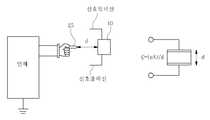
도 1은 종래 정전식 터치스크린 패널의 일예를 보여준다. 도 1을 참조하면, 플라스틱 또는 유리 등으로 제조된 투명기판(2)의 상하면에 투명도전막이 형성되며, 투명기판(2)의 네 모서리 각각에 전압인가용 금속전극(4)이 형성되어 있다. 상기 투명도전막은 ITO(Indium Tin Oxide) 등의 투명한 금속으로 형성된다. 그리고 상기 투명도전막의 네 모서리에 형성되는 금속전극(4)들은 은(Ag) 등의 저항률이 낮은 도전성 금속으로 프린팅하여 형성한다. 상기 금속전극(4)들의 주변에는 저항 네트워크가 형성된다.1 shows an example of a conventional capacitive touch screen panel. 1, a transparent conductive film is formed on the upper and lower surfaces of a
상기 저항 네트워크는 상기 투명도전막의 표면 전체에 균등하게 컨트롤신호를 송출하기 위하여 선형성 패턴(Linearization Pattern)으로 형성된다. 그리고 금속전극(4)을 포함한 투명도전막의 상부에는 보호막이 코팅된다.The resistance network is formed with a linearization pattern for uniformly transmitting a control signal to the entire surface of the transparent conductive film. A protective film is coated on the transparent conductive film including the
위와 같은 정전식 터치스크린 패널은 상기 금속전극(4)에 고주파의 교류 전압을 인가하면 이는 투명기판(2)의 전면에 퍼지게 된다. 이때 손가락(8)이나 도전성 터치입력도구로 투명기판(2) 상면의 투명도전막을 가볍게 터치하면, 일정량의 전류가 체내로 흡수되면서 컨트롤러(6)에 내장된 전류센서에서 전류의 변화를 감지하고 4개의 금속전극(4) 각각에서의 전류의 변화량을 연산하여 터치 지점을 인식하게 된다.When a high frequency AC voltage is applied to the
그런데, 도 1과 같은 정전식 터치스크린 패널은 미소 전류의 크기를 검출하는 방식으로서 검출 시스템이 고가이며, 하나의 터치드라이브IC로 터치스크린 패널의 전체 면적에 대해 터치신호를 검출할 수 있지만 복수 개의 터치를 인식하는 멀티터치가 어려운 문제점이 있다.The electrostatic touch screen panel as shown in FIG. 1 is a method of detecting the magnitude of the minute current, and the detection system is expensive. Although one touch drive IC can detect the touch signal with respect to the entire area of the touch screen panel, There is a problem that multi-touch which recognizes a touch is difficult.
이러한 문제점을 극복하기 위하여 근래에는 도 2와 같은 정전식 터치스크린 패널이 주로 사용되고 있다. 도 2의 터치스크린 패널은 횡방향의 선형센서패턴(5a) 및 종방향의 선형센서패턴(5b), 터치신호를 분석하는 터치드라이브IC(7a,7b)로 이루어져 있다. 이러한 터치스크린 패널은 선형센서패턴(5)과 손가락(8) 사이에 형성되는 커패시턴스의 크기를 검출하는 방식으로서, 횡방향의 선형센서패턴(5a)과 종방향의 선형센서패턴(5b)을 스캔하여 신호를 검출하므로 복수 개의 터치지점을 인식할 수 있다.In order to overcome such a problem, a capacitive touch screen panel as shown in FIG. 2 has been used in recent years. The touch screen panel of Fig. 2 comprises a
그러나, 터치스크린 패널이 큰 경우, 하나의 터치드라이브IC로 터치스크린 패널의 전 영역에서 터치 신호를 검출하는 것이 불가능하다. 예를 들어, 단일 터치드라이브IC를 사용하는 경우 터치스크린 패널이 넓어지면 선형센서패턴(5)의 면적도 넓어지므로 손가락과 대향하는 센서패턴(5)의 수가 적어지고 극단적인 경우, 손가락에 하나의 선형센서패턴(5)만이 접촉된다면 손가락 위치의 검출에 오류가 발생하는 선형성(linearity)이 불량한 현상이 발생하게 된다.However, when the touch screen panel is large, it is impossible to detect the touch signal in the entire area of the touch screen panel with one touch drive IC. For example, when a single touch-sensitive drive IC is used, the area of the
이러한 문제점을 극복하기 위해, 기존에는 도 3과 같이 복수 개의 터치드라이브IC(7a,7b)로 터치스크린 패널의 화면을 분할하여 터치를 검출하는 방법이 사용된다. 도 3을 참조하면, 터치패널(50) 상단부의“영역A"에서 터치를 검출하는 터치드라이브IC(7a)와, 하단부의 "영역B"를 검출하는 터치드라이브IC(7b)가 있으며, 복수 개의 터치드라이브IC(7a, 7b)를 제어하는 통합콘트롤러(11)가 구비된다.In order to overcome such a problem, a method of detecting a touch by dividing a screen of a touch screen panel by a plurality of
상기 통합콘트롤러(11)는 제어 및 통신선(8)을 통하여 터치드라이브IC(7a, 7b)들과 통신을 하거나 제어신호를 보내어, 터치드라이브IC(7a,7b)의 터치신호 검출에 관한 모든 동작을 제어하고, 터치드라이브IC(7a,7b)로 부터 터치 데이터를 전송받아 터치 좌표를 추출하는 역할을 한다.The integrated
그러나 이러한 구성은 별도의 통합 콘트롤러(11)를 사용해야 하므로 전류의 소모가 많고, 가격이 상승하게 되고, 통합 콘트롤러(11)의 실장을 위한 별도의 공간이 필요하다는 문제점이 있다.
However, this configuration requires a separate integrated
본 발명은 상술한 문제점을 해결하기 위하여 창출된 것으로, 본 발명의 목적은 외부로부터 터치패널에 방사된 정전기를 흡수하여 외부로 방전되도록 구비되어, 상기 정전기에 의한 터치 드라이브IC의 오작동 및 고장을 사전에 방지하며, 복수 개의 터치 드라이브IC 중 하나에 마스터 기능을 부여하여 나머지 슬레이브 터치 드라이브IC의 기능을 통제하기 위한 제어설계가 간소화되고 시스템 구축비용이 상대적으로 저렴한 ESD 기능이 구비된 터치스크린 패널을 제공하는 것에 있다.
SUMMARY OF THE INVENTION The present invention has been made in order to solve the above-mentioned problems, and it is an object of the present invention to provide a touch driver IC capable of absorbing static electricity radiated to the touch panel from the outside, And a touch screen panel having an ESD function that simplifies the control design for controlling the functions of the remaining slave touch driver ICs by providing the master function to one of the plurality of touch drive ICs and the system construction cost is relatively low .
본 발명의 특징에 따르면, 신체의 일부 또는 도전성 터치수단의 접근 또는 접촉을 감지하기 위한 소정의 센서패턴(10)이 형성되며, 경계부에 의해 복수 개의 개별영역으로 구획되는 터치패널(50); 및 상기 터치패널(50)의 각 개별영역별로 센서신호선(22)에 의해 신호연결되어 감지된 터치신호를 전달받으며, 그라운드 또는 소정의 전위에 접속되어 방전경로를 갖는 복수 개의 터치 드라이브IC(7a,7b);를 포함하되, 각 터치 드라이브IC(7a,7b)는, 스캔 시점(時點)과 스캔 지점(地點)을 동기화하기 위한 동기신호 및 상기 동기신호에 대한 피드백신호가 전송되는 동기신호선(17)과, 감지된 터치신호가 전송되는 터치신호선(15)에 의해 상호 신호연결되며, 상기 동기신호선(17) 및 터치신호선(15)은, 상기 터치패널(50) 상에서 정전기 유입의 시점에 해당하는 테두리 둘레에 배치되어 외부로부터 유입되는 정전기를 흡수하여 상기 방전경로를 통해 방전시키는 것을 특징으로 하는 ESD 기능이 구비된 터치스크린 패널이 제공된다.
According to an aspect of the present invention, there is provided a touch panel, comprising: a touch panel (50) formed with a predetermined sensor pattern (10) for sensing the approach or contact of a part of the body or conductive touch means and partitioned into a plurality of discrete regions by a boundary; And a plurality of touch drive ICs (7a, 7b) connected to the ground or to a predetermined potential and having a discharge path, wherein the plurality of touch drive ICs (7a, 7b) are connected to the touch panel (50) Each of the
본 발명의 다른 특징에 따르면, 신체의 일부 또는 도전성 터치수단의 접근 또는 접촉을 감지하기 위한 소정의 센서패턴(10)이 형성되며, 경계부에 의해 복수 개의 개별영역으로 구획되는 터치패널(50); 상기 터치패널(50)의 각 개별영역별로 센서신호선(22)에 의해 신호연결되어 감지된 터치신호를 전달받는 복수 개의 터치 드라이브IC(7a,7b); 및 상기 터치패널(50)에 접속되는 연성회로기판(19)을 통해 외부의 그라운드 또는 소정의 전위에 접속되며, 상기 터치패널(50) 상에서 정전기 유입의 시점에 해당하는 테두리 둘레에 배치되어 외부로부터 유입되는 정전기를 흡수하여 상기 연성회로기판(19)을 통해 방전시키는 ESD 흡수선(62);을 포함하는 ESD 기능이 구비된 터치스크린 패널이 제공된다.
According to another aspect of the present invention, there is provided a touch panel, comprising: a touch panel formed with a predetermined sensor pattern for detecting approach or contact of a body or a conductive touch means and partitioned into a plurality of individual regions by a boundary; A plurality of touch drive ICs (7a, 7b) receiving signals sensed by sensor signal lines (22) for each individual region of the touch panel (50) and receiving sensed touch signals; And a flexible circuit board (19) connected to the touch panel (50). The touch panel (50) is connected to an external ground or a predetermined electric potential, and is arranged around a rim And an ESD absorption line (62) for absorbing the introduced static electricity and discharging the static electricity through the flexible circuit board (19).
본 발명의 또 다른 특징에 따르면, 신체의 일부 또는 도전성 터치수단의 접근 또는 접촉을 감지하기 위한 소정의 센서패턴(10)이 형성되며, 경계부에 의해 복수 개의 개별영역으로 구획되는 터치패널(50); 상기 터치패널(50)의 각 개별영역별로 센서신호선(22)에 의해 신호연결되어 감지된 터치신호를 전달받으며, 그라운드 또는 소정의 전위에 접속되어 방전경로를 갖는 복수 개의 터치 드라이브IC(7a,7b);를 포함하되, 상기 복수 개의 터치 드라이브IC(7a,7b)에 접속되며, 상기 터치패널(50) 상에서 정전기 유입의 시점에 해당하는 테두리 둘레에 배치되어 외부로부터 유입되는 정전기를 흡수하여 상기 방전경로를 통해 방전시키는 ESD 흡수선(62);를 포함하는 ESD 기능이 구비된 터치스크린 패널이 제공된다.
According to another aspect of the present invention, there is provided a touch panel (50) formed with a predetermined sensor pattern (10) for detecting the approach or contact of a part of the body or conductive touch means, ; A plurality of
본 발명의 또 다른 특징에 따르면, 신체의 일부 또는 도전성 터치수단의 접근 또는 접촉을 감지하기 위한 소정의 센서패턴이 형성된 터치패널(50); 터치패널(50)과 센서신호선(22)에 의해 신호연결되어 감지된 터치신호를 전달받는 터치 드라이브IC(7); 및 상기 터치패널(50)에 접속되는 연성회로기판(19)을 통해 외부의 그라운드 또는 소정의 전위에 접속되며, 상기 터치패널(50) 상에서 정전기 유입의 시점에 해당하는 테두리 둘레에 배치되어 외부로부터 유입되는 정전기를 흡수하여 상기 연성회로기판(19)을 통해 방전시키는 ESD 흡수선(62);을 포함하는 ESD 기능이 구비된 터치스크린 패널이 제공된다.
According to another aspect of the present invention, there is provided a touch panel including: a touch panel having a sensor pattern formed thereon to detect a portion of a body or an approach or contact of a conductive touch means; A
본 발명의 또 다른 특징에 따르면, 신체의 일부 또는 도전성 터치수단의 접근 또는 접촉을 감지하기 위한 소정의 센서패턴이 형성된 터치패널(50); 상기 터치패널(50)과 센서신호선(22)에 의해 신호연결되어 감지된 터치신호를 전달받으며, 그라운드 또는 소정의 전위에 접속되어 방전경로를 갖는 터치 드라이브IC(7); 및 상기 터치 드라이브IC(7)에 접속되며, 상기 터치패널(50) 상에서 정전기 유입의 시점에 해당하는 테두리 둘레에 배치되어 외부로부터 유입되는 정전기를 흡수하여 상기 방전경로를 통해 방전시키는 ESD 흡수선(62);를 포함하는 ESD 기능이 구비된 터치스크린 패널이 제공된다.
According to another aspect of the present invention, there is provided a touch panel including: a touch panel having a sensor pattern formed thereon to detect a portion of a body or an approach or contact of a conductive touch means; A
이상에서와 같이, 외부로부터 터치패널에 방사된 정전기를 흡수하여 외부로 방전되도록 구비되어, 상기 정전기에 의한 터치 드라이브IC의 오작동 및 고장이 사전에 방지되는 효과를 구현할 수 있다.As described above, it is possible to absorb the static electricity radiated to the touch panel from the outside and to discharge it to the outside, so that malfunction and failure of the touch drive IC by the static electricity can be prevented in advance.
또한, 복수 개의 터치 드라이브IC 중 하나에 마스터 기능을 부여하여 나머지 슬레이브 터치 드라이브IC의 기능을 통제하기 위한 제어설계가 간소화되고 시스템 구축비용이 상대적으로 저렴한 장점이 있다.
In addition, a control function for controlling the functions of the remaining slave touch driver ICs is simplified by providing a master function to one of the plurality of touch drive ICs, and the system construction cost is relatively low.
도 1은 종래 정전식 터치스크린 패널의 일예를 보인 사시도
도 2는 종래 정전식 터치스크린 패널의 다른 예를 보인 평면구성도
도 3은 종래 복수의 IC를 사용하여 단일 터치스크린 패널의 터치신호를 검출하는 구성도
도 4는 본 발명의 바람직한 실시예에 따른 ESD 기능이 구비된 터치스크린 패널의 터치패널과 터치 드라이브IC의 구성을 나타낸 구성도,
도 5는 종래 정전식 터치스크린 패널의 일예를 보인 구성도,
도 6은 본 발명의 바람직한 실시예에 따른 터치스크린 패널의 터치신호 검출 시스템의 터치입력을 검출하는 원리를 예시한 개략도,
도 7은 본 발명의 바람직한 실시예에 따른 ESD 기능이 구비된 터치스크린 패널의 터치패널과 터치 드라이브IC의 다른 구성을 나타낸 구성도,
도 8은 본 발명의 바람직한 실시예에 따른 마스터 터치드라이브IC와 슬레이브 터치드라이브IC 간의 송수되는 신호의 예시를 나타낸 파형도,
도 9는 본 발명의 바람직한 실시예에 따른 ESD 기능이 구비된 터치스크린 패널과 과 표시장치의 결합된 상태를 나타낸 측면도,
도 11 내지 도 13은 본 발명의 바람직한 실시예에 따른 ESD 기능이 구비된 터치스크린 패널의 ESD 흡수선의 구성을 나타낸 구성도이다.1 is a perspective view showing an example of a conventional electrostatic touch screen panel.
2 is a plan view showing another example of a conventional capacitive touch screen panel
FIG. 3 is a configuration diagram of a conventional touch sensing device for detecting touch signals of a single touch screen panel using a plurality of ICs
FIG. 4 is a view illustrating a configuration of a touch panel and a touch drive IC of a touch screen panel having an ESD function according to a preferred embodiment of the present invention.
5 is a view showing an example of a conventional electrostatic touch screen panel,
6 is a schematic view illustrating a principle of detecting a touch input of a touch signal detection system of a touch screen panel according to a preferred embodiment of the present invention.
FIG. 7 is a view illustrating another structure of a touch panel and a touch drive IC of a touch screen panel having an ESD function according to a preferred embodiment of the present invention.
8 is a waveform diagram illustrating an example of a signal transmitted between a master touch drive IC and a slave touch drive IC according to a preferred embodiment of the present invention.
FIG. 9 is a side view illustrating a combined state of a touch screen panel having an ESD function and an overlay display device according to a preferred embodiment of the present invention. FIG.
FIGS. 11 to 13 are views illustrating a configuration of an ESD absorption line of a touch screen panel having an ESD function according to a preferred embodiment of the present invention.
상술한 본 발명의 목적, 특징들 및 장점은 다음의 상세한 설명을 통하여 보다 분명해질 것이다. 이하, 본 발명의 바람직한 실시예를 첨부한 도면에 의거하여 설명하면 다음과 같다.The objects, features and advantages of the present invention will become more apparent from the following detailed description. Hereinafter, preferred embodiments of the present invention will be described with reference to the accompanying drawings.
도 4는 본 발명의 바람직한 실시예에 따른 ESD 기능이 구비된 터치스크린 패널의 터치패널과 터치 드라이브IC의 구성을 나타낸 구성도, 도 6은 본 발명의 바람직한 실시예에 따른 터치스크린 패널의 터치신호 검출 시스템의 터치입력을 검출하는 원리를 예시한 개략도, 도 7은 본 발명의 바람직한 실시예에 따른 ESD 기능이 구비된 터치스크린 패널의 터치패널과 터치 드라이브IC의 다른 구성을 나타낸 구성도, 도 8은 본 발명의 바람직한 실시예에 따른 마스터 터치드라이브IC와 슬레이브 터치드라이브IC 간의 송수되는 신호의 예시를 나타낸 파형도, 도 9는 본 발명의 바람직한 실시예에 따른 ESD 기능이 구비된 터치스크린 패널과 과 표시장치의 결합된 상태를 나타낸 측면도, 도 11 내지 도 13은 본 발명의 바람직한 실시예에 따른 ESD 기능이 구비된 터치스크린 패널의 ESD 흡수선의 구성을 나타낸 구성도이다.
FIG. 4 is a configuration diagram of a touch panel and a touch drive IC of a touch screen panel having an ESD function according to a preferred embodiment of the present invention. FIG. 7 is a block diagram showing another configuration of a touch panel and a touch drive IC of a touch screen panel having an ESD function according to a preferred embodiment of the present invention. FIG. FIG. 9 is a waveform diagram illustrating an example of a signal transmitted between a master touch drive IC and a slave touch drive IC according to a preferred embodiment of the present invention. FIG. 9 is a diagram illustrating a touch screen panel having an ESD function according to a preferred embodiment of the present invention. FIG. 11 is a side view illustrating a combined state of the display device, FIG. 11 is a perspective view of a touch screen having an ESD function according to a preferred embodiment of the present invention, FIG. 2 is a configuration diagram showing a configuration of an ESD absorption line of a panel. FIG.
이하, 본 발명의 바람직한 실시예를 첨부된 도면 및 실시예를 참조하여 상세히 설명한다. 본 발명은 손가락이나 이와 유사한 전기적 특성을 갖는 도전성 터치수단의 비접촉 터치입력을 검출한다. 여기서 “비접촉 터치입력”이라 함은 손가락 등의 터치입력 수단이 터치스크린 패널에 의해 센서패턴과 소정 거리 이격된 상태에서 터치입력을 하는 것을 의미한다. 터치입력 수단이 터치스크린 패널의 외면에 대하여는 접촉될 수 있다. 하지만 이 경우에도 터치입력 수단과 센서패턴은 비접촉 상태를 유지한다. 따라서, 센서패턴에 대한 손가락의 터치 행위는 “접근”이라는 용어로 표현될 수 있다. 한편, 기판의 외면에 대하여는 손가락이 접촉된 상태일 수 있으므로, 기판에 대한 손가락의 터치 행위는 “접촉”이라는 용어로 표현될 수 있다. 본 명세서에서 “접근”과 “접촉”은 위와 같은 의미로 통용된다.Hereinafter, preferred embodiments of the present invention will be described in detail with reference to the accompanying drawings and embodiments. The present invention detects a noncontact touch input of a finger or a conductive touch means having similar electrical characteristics. Here, the term " noncontact touch input " means that a touch input means such as a finger or the like touches the touch panel while the touch input means is spaced apart from the sensor pattern by a predetermined distance. The touch input means can be brought into contact with the outer surface of the touch screen panel. In this case, however, the touch input means and the sensor pattern maintain the non-contact state. Thus, the touch behavior of a finger with respect to a sensor pattern can be expressed in terms of " approach ". On the other hand, since the finger may be in contact with the outer surface of the substrate, the touching action of the finger with respect to the substrate may be expressed by the term " contact ". As used herein, the terms " approach " and " contact "
또한 명세서 전체에서 터치신호선(15) 및 동기신호선(17)은 하나의 실선으로 표시되었으나, 터치신호선(15)의 경우에는 clock 및 in/out signal line 등 복수 개의 통신선이 사용될 수 있으며, 동기신호선(17)도 clock 또는 in/out 신호선 등 복수 개의 신호선이 사용될 수 있다.Although the
또한 명세서 전체에서 단지 두 개의 터치드라이브IC(7a,7b)를 사용하여 하나에는 마스터 기능을 부여하고 또 다른 하나에는 슬레이브 기능을 부여하였으나, 이는 도면을 간편하게 하기 위한 일 실시예일 뿐이며, 실제로는 세 개 이상되는 복수 개의 터치드라이브IC가 사용되어 하나에는 마스터 기능을 부여하고 나머지 터치드라이브IC에는 슬레이브 기능을 부여된 상태로 사용될 수 있다.In addition, in the entire specification, only two touch-
우선, 본 발명은 복수의 터치드라이브IC(7a,7b)로 단일 터치패널(50)의 터치신호를 검출하기 위한 ESD 기능이 구비된 터치스크린 패널에 관한 것으로, 종래에는 터치패널이 커서 하나의 터치드라이브IC로 터치 검출이 불가능할 때, 터치패널(50)의 감지영역을 복수 개로 분할하고 복수 개의 터치드라이브IC(7a,7b)로 각각의 감지 개별영역의 터치를 검출하며, 복수의 터치드라이브IC(7a,7b)를 제어하는 통합콘트롤러(11)를 필요로 하던 것을 복수의 터치드라이브IC(7a,7b) 중 하나는 마스터 기능을 갖고 나머지 터치드라이브IC(7b)는 슬레이브 기능을 갖도록 하여, 마스터 터치드라이브IC(7a)의 제어에 의해 슬레이브 터치드라이브IC(7b)가 터치 검출을 진행하고 마스터 터치드라이브IC(7a)와 슬레이브 터치드라이브IC(7b)간에 터치 검출을 위한 동기를 가능하게 해준다.The present invention relates to a touch screen panel having an ESD function for detecting a touch signal of a
최근에는 휴대용 기기가 보편화 되고 화면도 7인치 이상 대형화되면서, 하나의 터치드라이브IC로 7인치 이상되는 터치패널의 터치신호를 검출하기가 쉽지 않게 되었다. 이로 인해, 7인치 이상되는 터치패널에는 통상 서너 개의 터치드라이브IC를 사용하고, 터치패널의 화면을 복수 개의 감지영역으로 분할하여 분할된 터치패널의 감지영역별로 개별 터치드라브IC를 사용하고 통합콘트롤러(11)가 이들의 동작을 제어하고 또한 개별 터치드라이브IC가 검출한 터치신호를 모두 받아들여, 터치좌표를 연산하는 기능을 하게 된다.In recent years, with portable devices becoming commonplace and the screen becoming larger than 7 inches, it is not easy to detect a touch signal of a touch panel of 7 inches or more with a single touch drive IC. Therefore, a touch panel of seven or more inches usually uses three or four touch drive ICs, and the touch panel is divided into a plurality of sensing areas, and a separate touch driver IC is used for each sensing area of the divided touch panel, The
그러나, 통합 컨트롤러(11)는 터치제품에 적용하기 위한 전용제품이 아닌 경우가 대부분이며, 전용제품을 설계 및 제조하는 경우에도 사업규모가 작은 중소기업들은 이러한 전용의 통합콘트롤러(11)를 설계 및 제조하기가 어려우므로, 범용의 마이컴이나 CPU 등을 사용할 수 밖에 없다. 이러한 범용의 마이컴이나 CPU들은 소비전류가 과하기 때문에 이러한 통합콘트롤러(11)를 휴대용기기의 터치스크린 패널에 사용하는 경우 휴대용기기의 사용시간이 단축되어 휴대성이 저하된다는 문제점이 있다.However, in most cases, the
또한 휴대용 기기는 경박단소하므로, 작은 부품이라도 실장공간을 확보하기가 쉽지 않다. 더욱이 통합콘트롤러(11)는 연산을 위한 CPU가 포함되어야 하므로 통상 5mm x 5mm 이상 되는 패키지로 구성되어 있으며, 이러한 크기의 부품을 실장하기 위해서는 상당히 넓은 실장면적을 필요로 하며 실장위치 선정도 어려워진다.In addition, since portable equipment is light and thin, it is not easy to secure mounting space even for small parts. Further, since the
따라서, 상기와 같은 통합콘트롤러(11)를 사용하지 않고 복수의 터치드라이브IC(7a,7b)만으로 분할된 터치패널(50)의 터치검출을 가능하게 하는 수단을 제공함으로써, 소비전류가 감소하고 부품의 실장면적을 줄이고 제조원가가 절감되는 효과를 구현할 수 있다.Therefore, by providing means for enabling touch detection of the
도 4는 본 발명의 바람직한 실시예에 따른 ESD 기능이 구비된 터치스크린 패널의 터치패널과 터치 드라이브IC의 구성을 나타낸 구성도로서, Bar 타입의 단일 터치패널(50)의 경계부를 사이로 두 개의 터치드라이브IC(7a, 7b)가 사용된 경우이다. 터치패널(50)의 좌측에 위치한 마스터 터치드라이브IC(7a)는 터치패널(50)의 경계부 좌측 감지영역의 터치 신호를 검출하며, 터치패널(50)의 우측에 위치한 슬레이브 터치드라이브IC(7b)는 터치패널(50)의 경계부 우측 감지영역의 터치 신호를 검출한다.FIG. 4 is a diagram illustrating the configuration of a touch panel and a touch drive IC of a touch screen panel having an ESD function according to a preferred embodiment of the present invention. Referring to FIG. 4, Drive
여기서, 터치패널(50)의 경계부에서는 터치를 검출하기 위한 횡방향 센서패턴(10b)이 단절되어 있으며, 터치패널(50) 좌측의 센서패턴(10)은 마스터 터치드라이브IC(7a)에 접속되고, 터치패널(50) 우측의 센서패턴(10)은 슬레이브 터치드라이브IC(7b)에 접속되어 있다. 도 4의 센서신호선(22)은 센서패턴(10)과 터치드라이브IC(7a,7b)을 연결하는 수단이며, 센서패턴(10)에서 검출된 터치신호를 마스터 터치드라이브IC(7a) 및 슬레이브 터치드라이브IC(7b)로 전달하는 역할을 한다.The
도 5를 참조하면, 포인트방식의 터치검출부가 센서신호선(22)을 통해 터치드라이브IC(7a,7b)로 연결되어 있다. 도 2나 도 4의 실시예가 라인(line) 터치검출 방식인 것에 비해, 도 5의 센서패턴(10)은 포인트방식으로 되어 있으며, 이는 상용화된 정전식 터치방식의 또 다른 실시예이다.Referring to FIG. 5, a point-based touch detection unit is connected to the
한편, 도 6은 센서패턴(10)에서 정전식 터치를 검출하기 위한 터치스크린 패널의 터치신호 검출 시스템에 관한 실시예이다. 도 6의 실시예에서, 센서패턴(10)에 손가락(25) 또는 이와 유사한 도전성 터치수단이 접근했을 때, 센서패턴(10)과 손가락(25)이 "d"의 간격으로 이격되며, "A"라는 대향면적을 갖는다고 가정하면, 도 6의 우측 등가회로 및 수식에서 보여지듯이 손가락(25)과 센서패턴(10) 사이에는 정전용량 "C"가 형성된다. 정전용량 "C"를 가지는 센서패턴(10)의 신호입력선에 전압이나 전류의 신호를 공급하여 전하량 "Q"의 크기를 갖는 전하가 축적되면, V=Q/C라는 관계식이 형성되어 정전용량 "C"는 전하를 축적할 수 있다. 수식을 참조하면, 센서패턴(10)과 손가락 등의 터치수단(25)과의 접촉면적에 따라 정전용량의 차이가 발생하며, 정전용량의 차이는 축적되는 전하량의 차이를 유발하므로, 결국은 센서패턴(10)과 터치수단(25)과의 대향면적의 차이는 정전용량에서 검출되는 전압의 차이를 발생시킨다. 터치드라이브IC(7a,7b)는 이러한 전압의 차이를 검출하여 터치여부를 검출하게 된다.FIG. 6 is an embodiment of a touch signal detection system of a touch screen panel for detecting a capacitive touch in the
도 7은 도 5의 포인트 터치검출 방식의 터치드라이브IC(7a,7b)를 복수 개 사용하여, 단일 터치패널(50)에서 터치를 검출하기 위한 일 실시예이다. 도 7을 참조하면, 터치패널(50)은 경계부를 기준으로 2개의 감지 개별영역으로 분할되어 있으며, 좌측 감지영역의 터치신호를 검출하는 마스터 터치드라이브IC(7a)와 우측 감지영역의 터치신호를 검출하는 슬레이브 터치드라이브IC(7b)가 터치신호선(15) 및 동기신호선(17)에 의해 신호연결되도록 상호 접속되어 있다.7 is an embodiment for detecting a touch on a
도 4 또는 도 7을 참조하여 마스터와 슬레이브의 기능 및 터치 검출방법을 설명하면 다음과 같다. 우선, 도 4 또는 도 7의 복수 개의 터치드라이브IC는 사전에 마스터 터치드라이브IC(7a) 또는 슬레이브 터치드라이브IC(7b)로 정의되어야 한다. 이를 수행하기 위한 다양한 수단이 있겠으나 가장 손쉬운 방법은 터치드라이브IC(7a,7b) 내부에 레지스터 영역에서 마스터 터치드라이브IC(7a)와 슬레이브 터치드라이브IC(7b)를 설정하는 수단을 갖는 것이다. 예를 들면, 터치 드리이브 IC(7a,7b)의 레지스터의 특정영역에, “M/S”라고 하는 bit가 있다고 가정해 보자.The functions of the master and the slave and the touch detection method will be described with reference to FIG. 4 or FIG. First, the plurality of touch driver ICs shown in FIG. 4 or 7 should be defined as a master
이 bit가 “HI”면 마스터 터치드라이브IC(7a)로 동작하고 "LO"면 슬레이브 터치드라이브IC(7b)로 동작한다고 할 때, 이 bit를 사전에 HI나 LO로 설정하면 복수 개의 터치드라이브IC(7a,7b)에 개별적으로 마스터 터치드라이브IC(7a) 및 슬레이브 터치드라이브IC(7b)의 기능을 부여하도록 설정할 수 있는 것이다. 또 다른 방법의 실시예로서, 터치드라이브IC에 특정 pin을 할당하여 이들의 전위를 달리하는 방법이다. 만일 두 개의 pin을 이러한 용도로 사용하고자 할때, pin이 "00"로 설정된 경우에는 마스터 터치드라이브IC(7a)로 설정될 것이며, "01"인 경우에는 슬레이브 터치드라이브IC(7b)이면서 첫번째 드라이브IC로 설정될 수 있을 것이다. 또한 "10"인 경우에는 슬레이브드라이브IC이면서 두번째 드라이브IC로 자리매김될 수 있으며, "11"로 설정된 경우에는 세번째 슬레이브드라이브IC로 설정될 수 있다.If this bit is set to HI or LO when the bit is "HI" and the master
복수 개의 슬레이브 드라이브IC(7a,7b)가 사용되는 경우, 분할된 터치스크린패널(50)에서 각자의 위치가 정해져 있으므로 슬레이브 터치드라이브IC(7b)도 위치별로 번호가 다르게 할당되어야 한다. 후술하는 터치 신호선(15)을 통해 마스터 드라이브IC(7a)로 터치신호를 전송할 때, 통신 프로토콜에 슬레이브 드라이브IC(7b)의 위치를 삽입할 수 있으므로, 마스터 드라이브IC(7a)는 자신에게 전송된 신호를 분석할 때 분할된 터치스크린패널(50)의 어느 영역에서 전송된 신호인지를 판단하는 것이 가능하다.When a plurality of
도 4 또는 도 7에 실시예에 도시되어 있지는 않으나, 터치드라이브IC(7a,7b)는 CPU(40)와 연결되어야 한다. CPU(40)는 터치드라이브IC(7a,7b)로부터 터치좌표를 전송받아 터치패널(50)이 적용된 임의의 기기의 MP3 Palyer 기능을 동작시키거나 화면을 움직이거나 하는 등의 각종 실행동작을 시행하게 된다. 이러한 터치드라이브IC(7a,7b)와 CPU(40)와의 연결은 PCB나 연성회로기판(19)등을 이용하여 이루어지며 통상은 연성회로기판(19)을 이용하여 이루어진다. 이때 CPU(40)는 마스터 터치드라이브IC(7a)와 슬레이브 터치드라이브IC(7b) 각각에 접속될 수도 있겠으나, 연성회로기판(19)의 사용을 최소화하기 위하여 CPU(40)는 마스터 터치드라이브IC(7a)에만 접속될 수 있다. 이러한 경우 슬레이브 터치드라이브IC(7b)로 전달되는 정보는 마스터 터치드라이브IC(7a)를 경유하여 전달되어야 하므로, 마스터 터치드라이브IC(7a)와 슬레이브 터치드라이브IC(7b) 사이에는 터치신호선(15)이 존재하여야 한다. 상기 터치신호선(15)은 I2C나 SPI등의 serial통신이 사용되기도 하며 USB나 parallel 통신등 다양한 통신방법이 사용될 수 있으나 신호선의 개수를 줄이기 위하여 serial 통신을 사용하는 것이 바람직하다.Although not shown in the embodiment of FIG. 4 or 7, the touch-
상기 CPU(40)가 마스터 터치드라이브IC(7a)나 슬레이브 터치드라이브IC(7b)로 전송하는 데이터는 터치드라이브IC(7a,7b)의 동작에 필요한 레지스터 값들이거나 터치드라이브IC(7a,7b) 동작에 필요한 프로그램 등이다. 만일 마스터 터치드라이브IC(7a)의 레지스터 영역에 슬레이브 터치드라이브IC(7b)를 위한 레지스터 영역이 별도로 존재한다면, 마스터 터치드라이브IC(7a)는 이를 참조하여 슬레이브 터치드라이브IC(7b)가 필요로 하는 레지스터 값들을 터치신호선(15)을 통하여 슬레이브 터치드라이브IC(7b)로 전송할 수 있다.The data sent by the
또는 사전에 지정한 통신 프로토콜에 따라 CPU(40)로부터 마스터 드라이브IC(7a)로 전송된 data는 슬레이브 터치드라이브IC(7b)로 by-pass 될 수도 있다.Alternatively, the data transferred from the
만일 두 개 이상의 슬레이브 터치드라이브IC(7b)가 마스터 터치드라이브IC(7a)에 접속되어 있고, 각 슬레이브 터치드라이브IC(7b)마다 서로 다른 데이터를 기입하는 경우라고 하면, 각 슬레이브 터치드라이브IC(7b)에 ID를 부여하고 통신 프로토콜에 ID를 기입하면 슬레이브 터치드라이브IC(7b)는 자신과 동일한 ID의 데이터만 수납하도록 할 수도 있을 것이다.If two or more slave
이러한 터치신호선(15)은 터치패널(50) 내에 설치되어 마스터 터치드라이브IC(7a)와 슬레이브 터치드라이브IC(7b)롤 연결할 수도 있으며, 터치패널(50)의 외부를 통하여 마스터 터치드라이브IC(7a)와 슬레이브 터치드라이브IC(7b)를 연결할 수도 있다.The
후술하겠지만, 이러한 터치신호선(15)을 통하여 슬레이브 터치드라이브IC(7b)는 경계부의 터치데이터를 마스터 터치드라이브IC(7a)로 전송하고, 경계부에서도 마치 하나의 터치드라이브IC로 동작되는 것처럼 유연하게 터치동작이 될 수 있도록 터치데이터를 연산하여 터치좌표를 추출한다. 이러한 경계부에서의 데이터 처리를 위해서, 마스터 터치드라이브IC(7a)와 슬레이브 터치드라이브IC(7b)는 상호 동기되어야 하는데, 도 4를 참조하여 터치드라이브IC(7a,7b)간에 동기신호가 필요한 이유를 설명하면 다음과 같다.As will be described later, the slave
만일 복수의 터치드라이브IC(7a, 7b)가 현재 서로 동기가 되지 않은 상태라고 가정하고, 왼쪽의 마스터 드라이브IC(7a)는 C1에서 신호를 검출하고 있으며, 우측의 슬레이브 터치드라이브IC(7b)는 C11에서 터치신호를 검출하고 있다고 가정하자. 이때 손가락이 C11 ~ C12 에 터치된 상태이고 소정 시간 후에 터치패널(50)의 상단부로 이동하여 C9 ~ C10에 터치된 상태라고 가정한다. 우측의 슬레이브 터치드라이브IC(7b)는 C11 → C12 → C13의 경로를 스캔하고 있으므로 손가락에 의한 터치 신호를 검출하였으나, 좌측의 마스터 드라이브IC(7a)는 C1부터 스캔하여 C2 → C3 → C4...등의 경로를 스캔하고 있으므로 아직 손가락이 걸쳐진 C11을 스캔하지 못하여 터치 신호를 검출하지 못한 상태이다. 좌측의 마스터 터치드라이브IC(7a)가 C1부터 순차적으로 스캔하여 C9를 스캔하는 시간까지 소정의 시간이 필요하므로 이 시간동안 손가락은 터치패널(50)의 상방향으로 이동하여 C9와 C10에 위치하게 되었다. 이후 슬레이브 터치드라이브IC(7b)는 검출된 터치 데이터를 터치신호선(15)을 이용하여 마스터 드라이브IC(7a)로 전송하게 되고 마스터 드라이브IC(7a)는 경계부에서 검출된 자신의 터치 데이터와 슬레이브 터치드라이브IC(7b)의 터치 데이터를 분석하여 터치 좌표를 연산하게 된다.Assuming that the plurality of
이때, 마스터 드라이브IC(7a)는 C9에서 터치가 발생한 것을 검출하였고, 우측의 슬레이브 터치드라이브IC(7b)는 C11에서 터치가 발생한 것을 검출하였으므로, 마스터 드라이브IC(7a) C9와 C11의 양방향에서 마치 두 개의 터치가 발생한 것처럼 인식하게 된다.At this time, since the
도 7과 같은 포인트방식에서도 마스터 드라이브IC(7a)와 슬레이브 터치드라이브IC(7b)가 서로 동기되지 않으면 경계부에서 터치좌표 인식의 오류가 발생하는 것은 도 4의 실시예와 동일하며, 상세 설명은 생략한다.In the point system as shown in FIG. 7, if the
경계부에서, 하나의 터치에 대해 두 개의 멀티터치처럼 인식되는 이러한 문제점을 해결하기 위하여, 마스터 터치드라이브IC(7a)와 슬레이브 터치드라이브IC(7b)는 스캔 시점과 스캔 지점을 동일하게 일치시키는 과정인 동기화 과정을 필요로 한다. 만일 상술한 바와 같이, 마스터 터치드라이브IC(7a)와 슬레이브 터치드라이브IC(7b)가 C1부터(스캔지점의 동일화) 동일시점에(스캔시점의 동일화) 스캔을 시작한다면, 마스터 터치드라이브IC(7a)와 슬레이브 터치드라이브IC(7b) 모두 동일 시점 및 동일지점에서 손가락에 의한 터치를 검출하게 되므로 하나의 터치로 인식하게 되고 이를 시간의 추이에 따라 분석하면, 하나의 손가락이 터치패널(50)의 하부에서 상부로 이동하고 있음을 알아차릴 수 있다.In order to solve this problem, which is perceived as two multi-touches for one touch at the boundary, the master
마스터 터치드라이브IC(7a)와 슬레이브 터치드라이브IC(7b)가 동기되기 위해서는 동기 신호가 필요하며, 동기 신호는 마스터 터치드라이브IC(7a)가 생성하거나 슬레이브 터치드라이브IC(7b)가 생성할 수 있으며 통상은 마스터 터치드라이브IC(7a)가 생성한다. 생성된 동기신호는 터치신호선(15)을 통하여 슬레이브 터치드라이브IC(7b)로 전달되어 동기될 수도 있으나, 통상의 시리얼 통신이 빠르지 않음을 감안하면 별도의 동기신호선(17)을 사용하여 슬레이브 터치드라이브IC(7b)로 동기신호를 전송하는 것이 바람직하다.A synchronization signal is required for the master
동기신호는 특별한 규약을 필요로 하는 것은 아니나, 한 가지 실시예를 설명하면 도 8과 같다. 도 8을 참조하면, 마스터 드라이브IC(7a)의 스캔 시작점(도 4 또는 도 7의 실시예에서는 C1)에 대한 정보인 동기신호를 동기신호선(17)을 통하여 슬레이브 터치드라이브IC(7b)로 전송한다(start_master). 도 8에서 스캔 시작점은 두 개의 펄스로 표시되어 있으며, 이는 실시예에 불과하며 시작점임을 알리는 다양한 방법들이 사용될 수 있다. 예를 들면, 세 개의 펄스가 올 수도 있고 펄수 폭이 길어질수도 있고 또는 펄스 폭의 변조와 펄스 개수의 조합에 의해서도 달성될 수 있다.The synchronizing signal does not require a special protocol, but one embodiment will be described with reference to FIG. 8, a sync signal, which is information on the scan start point (C1 in the embodiment of FIG. 4 or FIG. 7) of the
슬레이브 터치드라이브IC(7b)는 마스터 터치드라이브IC(7a)로부터 받은 동기신호인 “start_master"에 대응하여 자신이 스캔 시작점을 인지했음을, 마스터 터치드라이브IC(7a)가 보낸 동일한 신호나 또는 사전에 규정된 임의의 신호인 피드백 신호를 동기신호선(17)을 통해 마스터 터치드라이브IC(7a)로 전송한다(start_slave). 이러한 이유는 노이즈에 의해 마스터 터치드라이브IC(7a)에서 슬레이브 터치드라이브IC(7b)로 전송되는 신호의 왜곡이 발생할 수 있으므로, 슬레이브 터치드라이브IC(7b)가 마스터 터치드라이브IC(7a)로 부터 전송된 신호를 정확히 받았는지를 확인하여 피드백(feedback)받은 신호의 유효성을 판단한다. The slave
한편, 스캔 시작점 이후의 각 라인별 스캔 시점도 마스터 드라이브IC(7a)는 슬레이브 터치드라이브IC(7b)로 동기신호선(17)을 통하여 전송할 수 있다. 도 8을 참조하면, 스캔 시작점 이후부터 순차적으로 발생하는 펄스는 C2 → C3...등을 순차적으로 스캔하는 동기신호이다. 이러한 동기신호를 마스터 터치드라이브IC(7a)로 부터 받은 슬레이브 터치드라이브IC(7b)는 동일한 신호나 사전에 규정된 신호를 마스터 터치드라이브IC(7a)로 전송하여 자신이 이상 없이 신호를 받았음을 마스터에게 고지한다. 마스터 터치드라이브IC(7a)와 슬레이브 터치드라이브IC(7b)는 서로의 통신이 완료된 후, 일정시점부터 동일하게 해당 라인에 대해 터치를 검출하면 앞의 실시예에서 스캔 신호의 비동기로 인해 발생했던 경계부에서의 검출에러가 발생하지 않게 된다.On the other hand, the scan time of each line after the scan start point can also be transmitted through the
이와 같이 마스터 드라이브IC(7a)와 슬레이브 터치드라이브IC(7b)가 상호 동기 된 후 경계부에서 검출된 슬레이브 터치드라이브IC(7b)의 데이터는 터치신호선(15)을 통하여 마스터 터치드라이브IC(7a)로 전송된다. 도 9는 슬레이브 터치드라이브IC(7b)가 경계부에서 검출된 데이터를 마스터 터치드라이브IC(7a)로 전송하는 데이터 형식에 관한 일 실시예이다. 도 9를 참조하면, 경계부에 터치수단인 손가락(25)이 접촉되었을 때 도 6의 수식에 따른 정전용량이 형성되고, 정전용량은 V=Q/C라고 하는 고전적인 수식에 의해 전압으로 환산되어, 터치드라이브IC(7a,7b) 내부의 신호처리부는 터치드라이브IC(7a,7b) 내부의 터치검출부에 포함된 ADC를 통해 전압을 읽는다. ADC를 통해 읽어 들인 각 센서패턴(10)의 전압은 정전용량으로 환산될 수도 있으며, 도 6의 수식에 의해 면적값으로 환산될 수 있다.After the
다시 도 9을 참조하면, 도 9는 도 7의 실시예에서 손가락이 센서패턴(10)을 터치했을 때, 각 단위 센서패턴(10)의 ADC 값이거나 또는 ADC 값을 면적으로 환산한 값 중의 하나이다. 경계부를 중심으로 좌측은 마스터 드라이브IC(7a)가 검출한 값이며 우측은 슬레이브 터치드라이브IC(7b)가 검출한 값이다.Referring again to FIG. 9, FIG. 9 is one of the ADC values of the
경계부에서 검출된 값을 이용하여 마스터 드라이브IC(7a) 또는 슬레이브 터치드라이브IC(7b)는 터치좌표를 추출해야 하며, 그러기 위해서 마스터 드라이브IC(7a)는 경계부에서의 모든 데이터를 필요로 한다. 본 발명에서는 이러한 통합 연산을 마스터 터치드라이브IC(7a)가 실시하므로 경계부에서의 데이터를 마스터 터치드라이브IC(7a)가 취합하는 것으로 가정하였으나 슬레이브 터치드라이브IC(7b)가 통합연산을 실시할 수도 있다.The
통합연산을 실시하기 위해 마스터 터치드라이브IC(7a)가 필요로 하는 데이터의 형태가 어떤 것인지 사전에 정의될 수 있다. 예컨대, 각 단위 센서패턴(10)의 ADC 값이나 면적값 또는 검출된 단위 센서패턴(10)들의 값을 종과 횡으로 모두 더한 값일 수도 있다.The type of data required by the master
다시 도 9를 참조하면, 경계부에서 마스터 드라이브IC(7a)와 슬레이브 터치드라이브IC(7b)에 의해 검출된 단위 센서패턴(10)의 ADC 값 또는 면적값이 표시되어 있다. 만일 마스터 드라이브IC(7a)가 이러한 단위 센서패턴(10)의 데이터를 필요로 한다면, 슬레이브 터치드라이브IC(7b)는 이들 데이터를 마스터 터치드라이브IC(7a)에게 터치신호선(15)을 통해 전송하면 된다. 마스터 드라이브IC(7a)는 전송받은 데이터와 자신이 가지고 있는 데이터가 이미 동기되어 있는 데이터이므로, 도 9와 같이 마스터 터치드라이브IC(7a)의 데이터와 슬레이브 터치드라이브IC(7b)의 데이터를 동일한 평면에 놓고 연산을 하면, 마치 하나의 드라이브 IC로 터치를 검출하는 것과 동일하게 터치를 검출하는 것이 가능하다.Referring again to FIG. 9, the ADC value or area value of the
한편, 단위 센서패턴(10)의 모든 데이터를 마스터 터치드라이브IC(7a)에게 전송하는 것은 데이터의 정확도가 향상된다는 장점은 있으나, 터치의 개수가 많아지면 데이터 양이 많아져서 마스터 터치드라이브IC(7a)로 전달되는 데어터의 전송 지연이 발생할 수 있다. 이는 연산속도의 저하를 유발하여 터치 속도가 저하되는 문제를 일으킨다.However, when the number of touches is increased, the amount of data increases, and the master
이러한 문제를 극복하기 위하여, 마스터 드라이브IC(7a)는 센서패턴(10)의 데이터를 종이나 횡의 합으로 받아들이고 이들 데이터를 기본으로 터치 중심점을 연산할 수도 있다. 이러한 방법은 슬레이브 터치드라이브IC(7b)가 마스터 터치드라이브IC(7a)로 전송하는 데이터의 양을 감소시켜 통신 지연으로 인한 터치속도 저하문제를 발생시키지 않는다. 도 9의 우측의 “60”과 “62”는 슬레이브 터치드라이브IC(7b)가 검출한 센서패턴(10)의 데이터를 횡방향으로 더한 것이며 “100”과 “17”은 슬레이브 터치드라이브IC(7b)가 검출하 센서패턴(10)의 데이터를 종방향으로 합산한 것이다. 도 9의 실시예에서는 슬레이브 터치드라이브IC(7b)에 의해 검출된 데이터의 개수가 4개 밖에 안되어 합산한 데이터의 양과 동일하게 보이지만 터치의 개수가 많을수록 종방향과 횡방향으로 합산한 데이터의 양은 적어지게 된다.In order to overcome such a problem, the
즉, 좌표가 많아질수록 좌표 data를 모두 보내는 것은 데이터가 많아서 속도저하문제가 발생하지만, 종과 횡으로 더한 양은 좌표가 많아질수록 상대적으로 갯수가 줄어든다는 의미한다.In other words, as the number of coordinates increases, the sending of all the coordinate data causes a problem of speed reduction due to a lot of data. However, the amount of the sum of the length and the width means that the number of the coordinates decreases relative to the number of the coordinates.
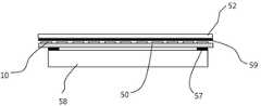
한편, 도 10은 터치패널(50)이 표시장치(58)의 상면에 부착된 실시예이다. 도10을 참조하면, 본 발명의 바람직한 실시예에 따른 터치패널(50)이 LCD 등의 표시장치(58)의 상면에 부착되는 경우, 터치패널(50)의 파손을 방지하는 보호유리 및 보호플라스틱 등의 보호판(52)이 터치패널(50)과 투과성양면 테잎(59)으로 접합된다. 이러한 구성에서, 사용자의 옷이나 주변환경에서 유발되거나, 또는 실험용 기기에서 유발된 정전기(ESD, Electro Static Discharge)가 상기 보호판(52) 등의 표면에 방사되면, 정전기는 유리 및 플라스틱 재질을 관통하지 못하므로 보호판(52)과 터치패널(50)이 접합되어 있는 에지(edge) 즉, 터치패널(50)의 테두리 둘레부터 침투하게 될 것이다. 침투가 시작되는 테두리 둘레부터 중심으로 정전기가 전달되므로 본 명세서에서는 터치패널(50)의 테두리 둘레부분을 정전기 유입의 시점(start point)이라고 정의한다. 만일 이러한 정전기가 센서패턴(10) 및 센서신호선(22)을 통하여 터치드라이브IC(7a,7b)로 유입되면 터치드라이브IC(7a,7b)의 오작동이나 고장을 유발하게 된다.On the other hand, Fig. 10 shows an embodiment in which the
이러한 정전기로 인한 터치드라이브IC(7a,7b)의 오작동이나 고장을 방지하기 위해, 정전기가 유입되는 경로의 시점에, 그라운드나 또는 임의의 DC나 AC 전위등 소정의 전위를 가진 배선이 존재한다면, 정전기는 배선을 통해 방전되고 배선 안쪽으로 유입되지 않을 것이다.In order to prevent malfunction or failure of the
도 11은 마스터 드라이브IC(7a)와 슬레이브 터치드라이브IC(7b) 간의 터치신호선(15)이나 동기신호선(17)을 이용하여 정전기의 유입을 방지하는 본 발명의 또 다른 실시예이다. 도 11을 참조하면, 터치신호선(15)이나 동기신호선(17)이 소기의 목적인 통신이나 제어신호선으로 사용되지 않는 휴지기에는, 터치신호선(15)이나 동기신호선(17)은 터치드라이브IC(7a,7b) 내부에서 그라운드 또는 DC나 AC 전압을 갖는 소정의 전위에 접속되며 방전경로를 갖고 있다. 예를 들어 DC는 0 ~ 수십 볼트 사이가 될 것이며 AC도 0 ~ 수십 볼트를 교번하는 교번전압이 될 것이다. 일반적으로 터치드라이브IC(7a,7b)에는 AC 전압이 없으므로, 그라운드나 DC 전압에 접속되는 것이 바람직하다.11 is another embodiment of the present invention for preventing the flow of static electricity by using the
터치신호선(15)이나 동기신호선(17)이 그라운드나 소정의 전위에 접속되어 있고 방전경로를 가진 상태에서, 정전기의 유입경로 시점에서 부터 터치패널(50) 전체를 감싸고 있으므로, 정전기가 터치장치의 유입되는 경우 이들 터치신호선(15)이나 동기신호선(17)에 의해 흡수되어 그라운드나 소정의 전위를 통해 방전되므로 터치패널(50)은 안전하게 보호된다.Since the
한편, 터치신호선(15)이나 동기신호선(17)을 이용한 정전기 방지방식에 있어서, 적어도 터치신호선(15)과 동기신호선(17) 둘 중에 하나는 통신동작이나 제어신호를 수반하는 동작을 하지 않아야 하며, 동작을 하지 않는 터치신호선(15) 또는 동기신호선(17)은 그라운드나 소정 전위를 가지는 전압에 접속되어야 한다.On the other hand, in the static electricity prevention system using the
도 4 또는 도 7의 실시예와 같이 터치신호선(15)이나 동기신호선(17)이 터치패널(50) 전체를 감싸지 못하는 경우, 또는 터치신호선(15)이나 동기신호선(17)이 지속적으로 마스터 터치드라이브IC(7a)와 슬레이브 터치드라이브IC(7b) 간의 통신에 할당되는 경우에는 터치신호선(15)이나 동기신호선(17)으로 정전기를 방지하는 기능을 구현하기가 어렵게 될 수 있다. 도 12는 이러한 문제점을 극복하기 위한 본 발명의 또 다른 실시예이다.When the
도 12를 참조하면, ESD 기능을 구현하기 위한 ESD 흡수선(62)이 별도로 배치되어 있으며 ESD 흡수선(62)은 연성회로기판(19)을 통하여 도시되지 않은 외부의 그라운드나 소정의 전위에 접속된다는 점이다. 도 12에는 ESD 흡수선(62)이 외부의 전위와 접속되는 것으로 표시되었으나, 터치드라이브IC(7a,7b)와 접속되어 터치드라이브IC(7a,7b)가 제공하는 그라운드나 소정의 전위에 접속될 수도 있다.12, an
다시 도 12를 참조하면. ESD 흡수선(62)은 터치패널(50)의 외곽인 정전기의 침투경로의 시점이 테두리 둘레의 침투경로 시점에 위치하는 것이 바람직하다. 도 11의 실시예인 터치신호선(15) 및 동기신호선(17) 들이 간헐적으로 그라운드나 소정의 전위에 접속되어 정전기가 침투될 수 있는 확률이 높은 것에 비해, 전용의 ESD 흡수선(62)은 항상 그라운드나 소정의 전위에 접속되어 있으므로 항상 정전기에 대한 방전대책이 가능하다.Referring back to FIG. It is preferable that the
도 13은 단일 터치드라이브IC(7)를 사용할 때 ESD 흡수선(62)이 적용된 경우의 실시예이다. 도 13을 참조하면 ESD 흡수선(62)이 연성회로기판(19)을 통하여 외부의 그라운드나 소정의 전위에 접속되었으며, 하나의 전위로 접속되거나 두 개의 서로 다른 외부 전위로 접속될 수 있다. 만일 서로 다른 외부의 전위로 접속된다면 ESD 흡수선(62)은 서로 분리되어야 할 것이며 하나의 전위로 접속되어도 폐루프(roop)를 형성하여 안테나 역할을 할 수 있으므로 서로 분리될 수도 있다. 도 13의 실시예는 ESD 흡수선(62)이 연성회로기판(19)을 통하여 외부의 전위와 연결되는 실시예를 설명하였으나, ESD 흡수선(62)은 터치드라이브IC(7a,7b)와 접속되어 터치드라이브IC(7a,7b)가 제공하는 그라운드 등의 전위에 접속될 수도 있다.13 shows an embodiment in which an
이상에서 설명한 본 발명은 전술한 실시예 및 첨부된 도면에 의해 한정되는 것이 아니고, 본 발명의 기술적 사상을 벗어나지 않는 범위 내에서 여러 가지 치환, 변형 및 변경이 가능함은 본 발명이 속하는 기술분야에서 통상의 지식을 가진 자에게 명백할 것이다.
It will be apparent to those skilled in the art that various modifications and variations can be made in the present invention without departing from the spirit or scope of the inventions. It will be apparent to those of ordinary skill in the art.
7 : 터치 드라이브IC7a : 마스터 터치드라이브IC
7b : 슬레이브 터치드라이브IC10 : 센서패턴
10a : 종방향 센서패턴10b : 횡방향 센서패턴
11 : 통합콘트롤러15 : 터치 신호선
17 : 동기신호선19 : 연성회로 기판
22 : 센서신호선25 : 손가락
40: CPU50 : 터치스크린 패널
52 : 보호유리 또는 보호플라스틱57 : 양면테잎
58 : 표시장치59 : 투과성양면 테잎
60 : 연성회로 기판62 : ESD 흡수선7:
7b: Slave touch drive IC 10: Sensor pattern
10a:
11: Integrated controller 15: Touch signal line
17: Synchronization signal line 19: Flexible circuit board
22: sensor signal line 25: finger
40: CPU 50: Touch screen panel
52: Protective glass or protective plastic 57: Double-sided tape
58: display device 59: transparent double-sided tape
60: flexible circuit board 62: ESD absorption line
Claims (6)
Translated fromKorean상기 터치패널(50)의 각 개별영역별로 센서신호선(22)에 의해 신호연결되어 감지된 터치신호를 전달받으며, 그라운드 또는 소정의 전위에 접속되어 방전경로를 갖는 복수 개의 터치 드라이브IC(7a,7b);를 포함하되,
상기 복수 개의 터치 드라이브IC(7a,7b)는, 마스터 터치드라이브IC(7a)의 동기 신호가 전송되는 동기신호선(17)과, 슬레이브 터치드라이브IC(7b)에서 감지된 터치신호가 전송되는 터치신호선(15)에 의해 상호 신호연결되며,
상기 동기신호선(17) 및 터치신호선(15)은, 상기 터치패널(50) 상에서 정전기 유입의 시점에 해당하는 테두리 둘레에 배치되어 외부로부터 유입되는 정전기를 흡수하여 상기 방전경로를 통해 방전시키는 것을 특징으로 하는 ESD 기능이 구비된 터치스크린 패널.
A touch panel (50) formed with a predetermined sensor pattern (10) for sensing the approach or contact of a part of the body or the conductive touch means and partitioned into a plurality of individual regions by a boundary portion; And
A plurality of touch drive ICs 7a and 7b (not shown) connected to the ground or to a predetermined potential to receive a touch signal sensed by the sensor signal line 22 for each individual region of the touch panel 50, ), ≪ / RTI >
The plurality of touch drive ICs 7a and 7b are connected to a synchronous signal line 17 through which a synchronous signal of the master touch drive IC 7a is transmitted and a touch signal line 17 through which a touch signal sensed by the slave touch- (15), respectively,
The synchronizing signal line 17 and the touch signal line 15 are disposed around the rim corresponding to the time point of the static charge on the touch panel 50 so as to absorb static electricity flowing from the outside and discharge the static electricity through the discharge path A touch screen panel having an ESD function.
상기 동기 신호선(17)은,
상기 마스터 터치드라이브IC(7a)와 슬레이브 터치드라이브IC(7b)의 스캔 시점(時點)과 스캔 지점(地點)을 동기화하기 위한 마스터 터치드라이브IC(7a)의 동기 신호가 전송되는 신호선인 것을 특징으로 하는 ESD 기능이 구비된 터치스크린 패널.
The method according to claim 1,
The synchronizing signal line (17)
Is a signal line through which a synchronization signal of a master touch drive IC 7a for synchronizing a scan point and a scan point of the master touch drive IC 7a and the slave touch drive IC 7b is transmitted A touch screen panel with ESD function.
상기 터치패널(50)의 각 개별영역별로 센서신호선(22)에 의해 신호연결되어 감지된 터치신호를 전달받는 복수 개의 터치 드라이브IC(7a,7b); 및
상기 터치패널(50)에 접속되는 연성회로기판(19)을 통해 외부의 그라운드 또는 소정의 전위에 접속되며, 상기 터치패널(50) 상에서 정전기 유입의 시점에 해당하는 테두리 둘레에 배치되어 외부로부터 유입되는 정전기를 흡수하여 상기 연성회로기판(19)을 통해 방전시키는 ESD 흡수선(62);을 포함하되,
상기 복수 개의 터치 드라이브IC(7a,7b)는, 마스터 터치드라이브IC(7a)의 동기 신호가 전송되는 동기신호선(17)과, 슬레이브 터치드라이브IC(7b)에서 감지된 터치신호가 전송되는 터치신호선(15)에 의해 상호 신호연결되어, 하나의 터치 드라이브IC(7a)는 마스터 기능을 갖고 나머지 터치 드라이브IC(7b)는 슬레이브 기능을 가지며, 마스터 터치 드라이브IC(7a)의 제어에 의해 슬레이브 터치 드라이브IC(7b)가 터치 검출을 진행하고 마스터 터치 드라이브IC(7a)와 슬레이브 터치 드라이브IC(7b) 간에 터치검출을 위한 동기가 구현되는 것을 특징으로 하는 ESD 기능이 구비된 터치스크린 패널.
A touch panel (50) formed with a predetermined sensor pattern (10) for sensing the approach or contact of a part of the body or the conductive touch means and partitioned into a plurality of individual regions by a boundary portion;
A plurality of touch drive ICs (7a, 7b) receiving signals sensed by sensor signal lines (22) for each individual region of the touch panel (50) and receiving sensed touch signals; And
Is connected to an external ground or a predetermined potential via a flexible circuit board (19) connected to the touch panel (50), and is arranged around a rim corresponding to a time point of static electricity inflow on the touch panel (50) And an ESD absorption line (62) for absorbing static electricity and discharging the static electricity through the flexible circuit board (19)
The plurality of touch drive ICs 7a and 7b are connected to a synchronous signal line 17 through which a synchronous signal of the master touch drive IC 7a is transmitted and a touch signal line 17 through which a touch signal sensed by the slave touch- One touch drive IC 7a has a master function and the remaining touch drive IC 7b has a slave function and the slave touch drive IC 7a is controlled by the master touch drive IC 7a, The IC 7b performs touch detection and the synchronization for touch detection is implemented between the master touch drive IC 7a and the slave touch drive IC 7b.
상기 터치패널(50)의 각 개별영역별로 센서신호선(22)에 의해 신호연결되어 감지된 터치신호를 전달받으며, 그라운드 또는 소정의 전위에 접속되어 방전경로를 갖는 복수 개의 터치 드라이브IC(7a,7b); 및
상기 복수 개의 터치 드라이브IC(7a,7b)에 접속되며, 상기 터치패널(50) 상에서 정전기 유입의 시점에 해당하는 테두리 둘레에 배치되어 외부로부터 유입되는 정전기를 흡수하여 상기 방전경로를 통해 방전시키는 ESD 흡수선(62);를 포함하되,
상기 복수 개의 터치 드라이브IC(7a,7b)는, 마스터 터치드라이브IC(7a)의 동기 신호가 전송되는 동기신호선(17)과, 슬레이브 터치드라이브IC(7b)에서 감지된 터치신호가 전송되는 터치신호선(15)에 의해 상호 신호연결되어, 하나의 터치 드라이브IC(7a)는 마스터 기능을 갖고 나머지 터치 드라이브IC(7b)는 슬레이브 기능을 가지며, 마스터 터치 드라이브IC(7a)의 제어에 의해 슬레이브 터치 드라이브IC(7b)가 터치 검출을 진행하고 마스터 터치 드라이브IC(7a)와 슬레이브 터치 드라이브IC(7b) 간에 터치검출을 위한 동기가 구현되는 것을 특징으로 하는 ESD 기능이 구비된 터치스크린 패널.
A touch panel (50) formed with a predetermined sensor pattern (10) for sensing the approach or contact of a part of the body or the conductive touch means and partitioned into a plurality of individual regions by a boundary portion;
A plurality of touch drive ICs 7a and 7b (not shown) connected to the ground or to a predetermined potential to receive a touch signal sensed by the sensor signal line 22 for each individual region of the touch panel 50, ); And
An ESD (Electrostatic Discharge) device which is connected to the plurality of touch drive ICs 7a and 7b and is disposed around a rim corresponding to a time point of the static electricity on the touch panel 50, discharges static electricity from the outside, And an absorption line (62)
The plurality of touch drive ICs 7a and 7b are connected to a synchronous signal line 17 through which a synchronous signal of the master touch drive IC 7a is transmitted and a touch signal line 17 through which a touch signal sensed by the slave touch- One touch drive IC 7a has a master function and the remaining touch drive IC 7b has a slave function and the slave touch drive IC 7a is controlled by the master touch drive IC 7a, The IC 7b performs touch detection and the synchronization for touch detection is implemented between the master touch drive IC 7a and the slave touch drive IC 7b.
Priority Applications (2)
| Application Number | Priority Date | Filing Date | Title |
|---|---|---|---|
| KR1020110070605AKR101426376B1 (en) | 2011-07-15 | 2011-07-15 | Touch Screen Panel With Electro Static Discharge |
| PCT/KR2012/005613WO2013012216A2 (en) | 2011-07-15 | 2012-07-13 | Touch screen panel having esd function |
Applications Claiming Priority (1)
| Application Number | Priority Date | Filing Date | Title |
|---|---|---|---|
| KR1020110070605AKR101426376B1 (en) | 2011-07-15 | 2011-07-15 | Touch Screen Panel With Electro Static Discharge |
Publications (2)
| Publication Number | Publication Date |
|---|---|
| KR20130009466A KR20130009466A (en) | 2013-01-23 |
| KR101426376B1true KR101426376B1 (en) | 2014-08-05 |
Family
ID=47558587
Family Applications (1)
| Application Number | Title | Priority Date | Filing Date |
|---|---|---|---|
| KR1020110070605AActiveKR101426376B1 (en) | 2011-07-15 | 2011-07-15 | Touch Screen Panel With Electro Static Discharge |
Country Status (2)
| Country | Link |
|---|---|
| KR (1) | KR101426376B1 (en) |
| WO (1) | WO2013012216A2 (en) |
Cited By (2)
| Publication number | Priority date | Publication date | Assignee | Title |
|---|---|---|---|---|
| US10282003B2 (en) | 2015-04-09 | 2019-05-07 | Samsung Display Co., Ltd. | Display device with touch sensor |
| CN108984023B (en)* | 2018-06-22 | 2021-08-10 | 武汉天马微电子有限公司 | Touch display panel and touch display device |
Families Citing this family (14)
| Publication number | Priority date | Publication date | Assignee | Title |
|---|---|---|---|---|
| KR102114329B1 (en)* | 2013-09-02 | 2020-05-25 | 엘지디스플레이 주식회사 | Touch sensing system and data compensation method thereof |
| CN103941908B (en)* | 2013-12-23 | 2017-03-08 | 上海天马微电子有限公司 | Touch screen display panel and touch screen display device |
| KR102175787B1 (en)* | 2013-12-27 | 2020-11-06 | 엘지디스플레이 주식회사 | Touch screen and display device including the same |
| KR102291466B1 (en) | 2015-01-20 | 2021-08-19 | 삼성디스플레이 주식회사 | Touch screen panel |
| KR102383821B1 (en)* | 2015-04-17 | 2022-04-06 | 주식회사 엘엑스세미콘 | Touch system and touch ic for sharing data, and control method thereof |
| CN104850270B (en) | 2015-06-11 | 2017-10-03 | 京东方科技集团股份有限公司 | Driving method, drive circuit, touch module, panel and the device of touch module |
| KR102625980B1 (en)* | 2016-10-04 | 2024-01-16 | 엘지디스플레이 주식회사 | Display device |
| KR102690479B1 (en)* | 2016-12-26 | 2024-07-31 | 엘지디스플레이 주식회사 | Touch panel liquid crystal display device |
| CN109917942A (en)* | 2017-12-13 | 2019-06-21 | 南昌欧菲显示科技有限公司 | Pressure sensing assembly, touch screen and mobile terminal |
| KR102513752B1 (en)* | 2018-04-11 | 2023-03-24 | 삼성전자 주식회사 | Electronic apparatus and controlling method thereof |
| CN109377933B (en)* | 2018-12-26 | 2022-01-14 | 厦门天马微电子有限公司 | Display panel driving method, display panel and display device |
| KR102371033B1 (en)* | 2020-07-22 | 2022-03-04 | 동우 화인켐 주식회사 | Antenna-inserted electrode structure and image display device including the same |
| CN112051936B (en)* | 2020-08-21 | 2024-05-28 | 维信诺科技股份有限公司 | Display device |
| KR20220106892A (en) | 2021-01-22 | 2022-08-01 | 삼성디스플레이 주식회사 | Display device |
Citations (2)
| Publication number | Priority date | Publication date | Assignee | Title |
|---|---|---|---|---|
| KR20110041109A (en)* | 2009-10-15 | 2011-04-21 | 엘지디스플레이 주식회사 | Touch panel |
| KR20110066450A (en)* | 2009-12-11 | 2011-06-17 | 엘지디스플레이 주식회사 | Touch panel and touch panel integrated liquid crystal display |
Family Cites Families (2)
| Publication number | Priority date | Publication date | Assignee | Title |
|---|---|---|---|---|
| JP5031797B2 (en)* | 2009-06-18 | 2012-09-26 | 株式会社デジタル | Touch panel drive device and touch panel device |
| KR101076236B1 (en)* | 2009-06-29 | 2011-10-26 | 주식회사 포인칩스 | Capacitance type touch panel |
- 2011
- 2011-07-15KRKR1020110070605Apatent/KR101426376B1/enactiveActive
- 2012
- 2012-07-13WOPCT/KR2012/005613patent/WO2013012216A2/enactiveApplication Filing
Patent Citations (2)
| Publication number | Priority date | Publication date | Assignee | Title |
|---|---|---|---|---|
| KR20110041109A (en)* | 2009-10-15 | 2011-04-21 | 엘지디스플레이 주식회사 | Touch panel |
| KR20110066450A (en)* | 2009-12-11 | 2011-06-17 | 엘지디스플레이 주식회사 | Touch panel and touch panel integrated liquid crystal display |
Cited By (3)
| Publication number | Priority date | Publication date | Assignee | Title |
|---|---|---|---|---|
| US10282003B2 (en) | 2015-04-09 | 2019-05-07 | Samsung Display Co., Ltd. | Display device with touch sensor |
| US11226693B2 (en) | 2015-04-09 | 2022-01-18 | Samsung Display Co., Ltd. | Display device with touch sensor |
| CN108984023B (en)* | 2018-06-22 | 2021-08-10 | 武汉天马微电子有限公司 | Touch display panel and touch display device |
Also Published As
| Publication number | Publication date |
|---|---|
| WO2013012216A2 (en) | 2013-01-24 |
| KR20130009466A (en) | 2013-01-23 |
| WO2013012216A3 (en) | 2013-04-11 |
Similar Documents
| Publication | Publication Date | Title |
|---|---|---|
| KR101426376B1 (en) | Touch Screen Panel With Electro Static Discharge | |
| KR102023841B1 (en) | Electrical device having multi-functional human interface | |
| US8130202B2 (en) | Infrared touch screen gated by touch force | |
| US8994687B2 (en) | Mutual-capacitance touch sensing device and electronic system including the same | |
| KR100628265B1 (en) | Resistive Touch Panel | |
| CN104571748B (en) | Touch controller, electronic device and display device, and touch sensing method | |
| KR101637422B1 (en) | Touch screen panel | |
| US20140362034A1 (en) | Touch display device | |
| KR20160000100A (en) | Touch panel and apparatus for driving thereof | |
| KR20110111192A (en) | Method and apparatus for forming electrode pattern in touch panel | |
| US20140145978A1 (en) | Touch panel having virtual function button, method of manufacturing the same, and method of identifying touch conflict on the same | |
| KR20130124084A (en) | Sensor for detecting proximity/motion and touch and display device having the same | |
| CN102402326A (en) | Touch tracking across multiple touch screens | |
| KR102133453B1 (en) | Touch sensor including electrostatic discharge pattern | |
| CN104345998A (en) | Drive induction method of single layer multipoint mutual capacitive touch screen | |
| KR101310744B1 (en) | System To Detect Touch Signal Of Touch Screen Panel | |
| US11614839B2 (en) | Balanced mutual capacitance systems and methods | |
| US9372587B2 (en) | Methods and apparatus for arranging electrode layers and associated routing traces in a sensor device | |
| KR101403421B1 (en) | System To Detect Touch Signal Of Touch Screen Panel | |
| KR20170069022A (en) | Display Device | |
| KR102320770B1 (en) | Touch recognition mehtod for display device and display device using the same | |
| KR101119386B1 (en) | Touch screen | |
| KR20190034942A (en) | Self-capacitance Touch Screen | |
| KR20170138160A (en) | Display apparatus | |
| KR20160047682A (en) | Touch screen device and method for driving thereof |
Legal Events
| Date | Code | Title | Description |
|---|---|---|---|
| A201 | Request for examination | ||
| PA0109 | Patent application | St.27 status event code:A-0-1-A10-A12-nap-PA0109 | |
| PA0201 | Request for examination | St.27 status event code:A-1-2-D10-D11-exm-PA0201 | |
| R18-X000 | Changes to party contact information recorded | St.27 status event code:A-3-3-R10-R18-oth-X000 | |
| R18-X000 | Changes to party contact information recorded | St.27 status event code:A-3-3-R10-R18-oth-X000 | |
| E902 | Notification of reason for refusal | ||
| PE0902 | Notice of grounds for rejection | St.27 status event code:A-1-2-D10-D21-exm-PE0902 | |
| PG1501 | Laying open of application | St.27 status event code:A-1-1-Q10-Q12-nap-PG1501 | |
| T11-X000 | Administrative time limit extension requested | St.27 status event code:U-3-3-T10-T11-oth-X000 | |
| AMND | Amendment | ||
| P11-X000 | Amendment of application requested | St.27 status event code:A-2-2-P10-P11-nap-X000 | |
| P13-X000 | Application amended | St.27 status event code:A-2-2-P10-P13-nap-X000 | |
| E601 | Decision to refuse application | ||
| PE0601 | Decision on rejection of patent | St.27 status event code:N-2-6-B10-B15-exm-PE0601 | |
| AMND | Amendment | ||
| E13-X000 | Pre-grant limitation requested | St.27 status event code:A-2-3-E10-E13-lim-X000 | |
| P11-X000 | Amendment of application requested | St.27 status event code:A-2-2-P10-P11-nap-X000 | |
| P13-X000 | Application amended | St.27 status event code:A-2-2-P10-P13-nap-X000 | |
| PX0901 | Re-examination | St.27 status event code:A-2-3-E10-E12-rex-PX0901 | |
| E902 | Notification of reason for refusal | ||
| PE0902 | Notice of grounds for rejection | St.27 status event code:A-1-2-D10-D21-exm-PE0902 | |
| AMND | Amendment | ||
| P11-X000 | Amendment of application requested | St.27 status event code:A-2-2-P10-P11-nap-X000 | |
| P13-X000 | Application amended | St.27 status event code:A-2-2-P10-P13-nap-X000 | |
| PX0701 | Decision of registration after re-examination | St.27 status event code:A-3-4-F10-F13-rex-PX0701 | |
| X701 | Decision to grant (after re-examination) | ||
| GRNT | Written decision to grant | ||
| PR0701 | Registration of establishment | St.27 status event code:A-2-4-F10-F11-exm-PR0701 | |
| PR1002 | Payment of registration fee | Fee payment year number:1 St.27 status event code:A-2-2-U10-U11-oth-PR1002 | |
| PG1601 | Publication of registration | St.27 status event code:A-4-4-Q10-Q13-nap-PG1601 | |
| PC1903 | Unpaid annual fee | Not in force date:20170730 Payment event data comment text:Termination Category : DEFAULT_OF_REGISTRATION_FEE St.27 status event code:A-4-4-U10-U13-oth-PC1903 | |
| FPAY | Annual fee payment | Payment date:20180426 Year of fee payment:4 | |
| K11-X000 | Ip right revival requested | St.27 status event code:A-6-4-K10-K11-oth-X000 | |
| PC1903 | Unpaid annual fee | Ip right cessation event data comment text:Termination Category : DEFAULT_OF_REGISTRATION_FEE Not in force date:20170730 St.27 status event code:N-4-6-H10-H13-oth-PC1903 | |
| PR0401 | Registration of restoration | St.27 status event code:A-6-4-K10-K13-oth-PR0401 | |
| R401 | Registration of restoration | ||
| PR1001 | Payment of annual fee | Fee payment year number:4 St.27 status event code:A-4-4-U10-U11-oth-PR1001 | |
| FPAY | Annual fee payment | Payment date:20180625 Year of fee payment:5 | |
| PR1001 | Payment of annual fee | Fee payment year number:5 St.27 status event code:A-4-4-U10-U11-oth-PR1001 | |
| FPAY | Annual fee payment | Payment date:20190729 Year of fee payment:6 | |
| PR1001 | Payment of annual fee | Fee payment year number:6 St.27 status event code:A-4-4-U10-U11-oth-PR1001 | |
| PR1001 | Payment of annual fee | Fee payment year number:7 St.27 status event code:A-4-4-U10-U11-oth-PR1001 | |
| PR1001 | Payment of annual fee | Fee payment year number:8 St.27 status event code:A-4-4-U10-U11-oth-PR1001 | |
| P22-X000 | Classification modified | St.27 status event code:A-4-4-P10-P22-nap-X000 | |
| PR1001 | Payment of annual fee | Fee payment year number:9 St.27 status event code:A-4-4-U10-U11-oth-PR1001 | |
| PR1001 | Payment of annual fee | Fee payment year number:10 St.27 status event code:A-4-4-U10-U11-oth-PR1001 | |
| PR1001 | Payment of annual fee | Fee payment year number:11 St.27 status event code:A-4-4-U10-U11-oth-PR1001 | |
| PR1001 | Payment of annual fee | Fee payment year number:12 St.27 status event code:A-4-4-U10-U11-oth-PR1001 |