KR101426285B1 - Optical Transmission / Reception Device and Manufacturing Method Thereof - Google Patents
Optical Transmission / Reception Device and Manufacturing Method ThereofDownload PDFInfo
- Publication number
- KR101426285B1 KR101426285B1KR1020080002640AKR20080002640AKR101426285B1KR 101426285 B1KR101426285 B1KR 101426285B1KR 1020080002640 AKR1020080002640 AKR 1020080002640AKR 20080002640 AKR20080002640 AKR 20080002640AKR 101426285 B1KR101426285 B1KR 101426285B1
- Authority
- KR
- South Korea
- Prior art keywords
- laser diode
- layer
- photodiode
- substrate
- forming
- Prior art date
- Legal status (The legal status is an assumption and is not a legal conclusion. Google has not performed a legal analysis and makes no representation as to the accuracy of the status listed.)
- Active
Links
Images


Classifications
- H—ELECTRICITY
- H10—SEMICONDUCTOR DEVICES; ELECTRIC SOLID-STATE DEVICES NOT OTHERWISE PROVIDED FOR
- H10F—INORGANIC SEMICONDUCTOR DEVICES SENSITIVE TO INFRARED RADIATION, LIGHT, ELECTROMAGNETIC RADIATION OF SHORTER WAVELENGTH OR CORPUSCULAR RADIATION
- H10F55/00—Radiation-sensitive semiconductor devices covered by groups H10F10/00, H10F19/00 or H10F30/00 being structurally associated with electric light sources and electrically or optically coupled thereto
- H10F55/18—Radiation-sensitive semiconductor devices covered by groups H10F10/00, H10F19/00 or H10F30/00 being structurally associated with electric light sources and electrically or optically coupled thereto wherein the radiation-sensitive semiconductor devices and the electric light source share a common body having dual-functionality of light emission and light detection
- H—ELECTRICITY
- H01—ELECTRIC ELEMENTS
- H01S—DEVICES USING THE PROCESS OF LIGHT AMPLIFICATION BY STIMULATED EMISSION OF RADIATION [LASER] TO AMPLIFY OR GENERATE LIGHT; DEVICES USING STIMULATED EMISSION OF ELECTROMAGNETIC RADIATION IN WAVE RANGES OTHER THAN OPTICAL
- H01S5/00—Semiconductor lasers
- H01S5/10—Construction or shape of the optical resonator, e.g. extended or external cavity, coupled cavities, bent-guide, varying width, thickness or composition of the active region
- H01S5/18—Surface-emitting [SE] lasers, e.g. having both horizontal and vertical cavities
- H01S5/183—Surface-emitting [SE] lasers, e.g. having both horizontal and vertical cavities having only vertical cavities, e.g. vertical cavity surface-emitting lasers [VCSEL]
- H—ELECTRICITY
- H01—ELECTRIC ELEMENTS
- H01L—SEMICONDUCTOR DEVICES NOT COVERED BY CLASS H10
- H01L24/00—Arrangements for connecting or disconnecting semiconductor or solid-state bodies; Methods or apparatus related thereto
- H01L24/01—Means for bonding being attached to, or being formed on, the surface to be connected, e.g. chip-to-package, die-attach, "first-level" interconnects; Manufacturing methods related thereto
- H01L24/10—Bump connectors ; Manufacturing methods related thereto
- H01L24/12—Structure, shape, material or disposition of the bump connectors prior to the connecting process
- H01L24/14—Structure, shape, material or disposition of the bump connectors prior to the connecting process of a plurality of bump connectors
- H—ELECTRICITY
- H01—ELECTRIC ELEMENTS
- H01S—DEVICES USING THE PROCESS OF LIGHT AMPLIFICATION BY STIMULATED EMISSION OF RADIATION [LASER] TO AMPLIFY OR GENERATE LIGHT; DEVICES USING STIMULATED EMISSION OF ELECTROMAGNETIC RADIATION IN WAVE RANGES OTHER THAN OPTICAL
- H01S5/00—Semiconductor lasers
- H01S5/02—Structural details or components not essential to laser action
- H01S5/026—Monolithically integrated components, e.g. waveguides, monitoring photo-detectors, drivers
- H01S5/0262—Photo-diodes, e.g. transceiver devices, bidirectional devices
- H—ELECTRICITY
- H01—ELECTRIC ELEMENTS
- H01S—DEVICES USING THE PROCESS OF LIGHT AMPLIFICATION BY STIMULATED EMISSION OF RADIATION [LASER] TO AMPLIFY OR GENERATE LIGHT; DEVICES USING STIMULATED EMISSION OF ELECTROMAGNETIC RADIATION IN WAVE RANGES OTHER THAN OPTICAL
- H01S5/00—Semiconductor lasers
- H01S5/10—Construction or shape of the optical resonator, e.g. extended or external cavity, coupled cavities, bent-guide, varying width, thickness or composition of the active region
- H01S5/18—Surface-emitting [SE] lasers, e.g. having both horizontal and vertical cavities
- H01S5/183—Surface-emitting [SE] lasers, e.g. having both horizontal and vertical cavities having only vertical cavities, e.g. vertical cavity surface-emitting lasers [VCSEL]
- H01S5/18305—Surface-emitting [SE] lasers, e.g. having both horizontal and vertical cavities having only vertical cavities, e.g. vertical cavity surface-emitting lasers [VCSEL] with emission through the substrate, i.e. bottom emission
- H—ELECTRICITY
- H10—SEMICONDUCTOR DEVICES; ELECTRIC SOLID-STATE DEVICES NOT OTHERWISE PROVIDED FOR
- H10F—INORGANIC SEMICONDUCTOR DEVICES SENSITIVE TO INFRARED RADIATION, LIGHT, ELECTROMAGNETIC RADIATION OF SHORTER WAVELENGTH OR CORPUSCULAR RADIATION
- H10F30/00—Individual radiation-sensitive semiconductor devices in which radiation controls the flow of current through the devices, e.g. photodetectors
- H10F30/20—Individual radiation-sensitive semiconductor devices in which radiation controls the flow of current through the devices, e.g. photodetectors the devices having potential barriers, e.g. phototransistors
- H—ELECTRICITY
- H10—SEMICONDUCTOR DEVICES; ELECTRIC SOLID-STATE DEVICES NOT OTHERWISE PROVIDED FOR
- H10F—INORGANIC SEMICONDUCTOR DEVICES SENSITIVE TO INFRARED RADIATION, LIGHT, ELECTROMAGNETIC RADIATION OF SHORTER WAVELENGTH OR CORPUSCULAR RADIATION
- H10F71/00—Manufacture or treatment of devices covered by this subclass
- H10F71/127—The active layers comprising only Group III-V materials, e.g. GaAs or InP
- H—ELECTRICITY
- H01—ELECTRIC ELEMENTS
- H01L—SEMICONDUCTOR DEVICES NOT COVERED BY CLASS H10
- H01L2224/00—Indexing scheme for arrangements for connecting or disconnecting semiconductor or solid-state bodies and methods related thereto as covered by H01L24/00
- H01L2224/01—Means for bonding being attached to, or being formed on, the surface to be connected, e.g. chip-to-package, die-attach, "first-level" interconnects; Manufacturing methods related thereto
- H01L2224/10—Bump connectors; Manufacturing methods related thereto
- H01L2224/15—Structure, shape, material or disposition of the bump connectors after the connecting process
- H01L2224/16—Structure, shape, material or disposition of the bump connectors after the connecting process of an individual bump connector
- H01L2224/161—Disposition
- H01L2224/16151—Disposition the bump connector connecting between a semiconductor or solid-state body and an item not being a semiconductor or solid-state body, e.g. chip-to-substrate, chip-to-passive
- H01L2224/16221—Disposition the bump connector connecting between a semiconductor or solid-state body and an item not being a semiconductor or solid-state body, e.g. chip-to-substrate, chip-to-passive the body and the item being stacked
- H01L2224/16225—Disposition the bump connector connecting between a semiconductor or solid-state body and an item not being a semiconductor or solid-state body, e.g. chip-to-substrate, chip-to-passive the body and the item being stacked the item being non-metallic, e.g. insulating substrate with or without metallisation
- H—ELECTRICITY
- H01—ELECTRIC ELEMENTS
- H01L—SEMICONDUCTOR DEVICES NOT COVERED BY CLASS H10
- H01L2924/00—Indexing scheme for arrangements or methods for connecting or disconnecting semiconductor or solid-state bodies as covered by H01L24/00
- H01L2924/10—Details of semiconductor or other solid state devices to be connected
- H01L2924/11—Device type
- H01L2924/12—Passive devices, e.g. 2 terminal devices
- H01L2924/1204—Optical Diode
- H01L2924/12043—Photo diode
- H—ELECTRICITY
- H01—ELECTRIC ELEMENTS
- H01S—DEVICES USING THE PROCESS OF LIGHT AMPLIFICATION BY STIMULATED EMISSION OF RADIATION [LASER] TO AMPLIFY OR GENERATE LIGHT; DEVICES USING STIMULATED EMISSION OF ELECTROMAGNETIC RADIATION IN WAVE RANGES OTHER THAN OPTICAL
- H01S2301/00—Functional characteristics
- H01S2301/17—Semiconductor lasers comprising special layers
- H01S2301/176—Specific passivation layers on surfaces other than the emission facet
- H—ELECTRICITY
- H01—ELECTRIC ELEMENTS
- H01S—DEVICES USING THE PROCESS OF LIGHT AMPLIFICATION BY STIMULATED EMISSION OF RADIATION [LASER] TO AMPLIFY OR GENERATE LIGHT; DEVICES USING STIMULATED EMISSION OF ELECTROMAGNETIC RADIATION IN WAVE RANGES OTHER THAN OPTICAL
- H01S5/00—Semiconductor lasers
- H01S5/02—Structural details or components not essential to laser action
- H01S5/0206—Substrates, e.g. growth, shape, material, removal or bonding
- H01S5/0217—Removal of the substrate
- H—ELECTRICITY
- H01—ELECTRIC ELEMENTS
- H01S—DEVICES USING THE PROCESS OF LIGHT AMPLIFICATION BY STIMULATED EMISSION OF RADIATION [LASER] TO AMPLIFY OR GENERATE LIGHT; DEVICES USING STIMULATED EMISSION OF ELECTROMAGNETIC RADIATION IN WAVE RANGES OTHER THAN OPTICAL
- H01S5/00—Semiconductor lasers
- H01S5/02—Structural details or components not essential to laser action
- H01S5/022—Mountings; Housings
- H01S5/0225—Out-coupling of light
- H01S5/02251—Out-coupling of light using optical fibres
- H—ELECTRICITY
- H01—ELECTRIC ELEMENTS
- H01S—DEVICES USING THE PROCESS OF LIGHT AMPLIFICATION BY STIMULATED EMISSION OF RADIATION [LASER] TO AMPLIFY OR GENERATE LIGHT; DEVICES USING STIMULATED EMISSION OF ELECTROMAGNETIC RADIATION IN WAVE RANGES OTHER THAN OPTICAL
- H01S5/00—Semiconductor lasers
- H01S5/02—Structural details or components not essential to laser action
- H01S5/022—Mountings; Housings
- H01S5/0233—Mounting configuration of laser chips
- H01S5/0234—Up-side down mountings, e.g. Flip-chip, epi-side down mountings or junction down mountings
- H—ELECTRICITY
- H01—ELECTRIC ELEMENTS
- H01S—DEVICES USING THE PROCESS OF LIGHT AMPLIFICATION BY STIMULATED EMISSION OF RADIATION [LASER] TO AMPLIFY OR GENERATE LIGHT; DEVICES USING STIMULATED EMISSION OF ELECTROMAGNETIC RADIATION IN WAVE RANGES OTHER THAN OPTICAL
- H01S5/00—Semiconductor lasers
- H01S5/02—Structural details or components not essential to laser action
- H01S5/022—Mountings; Housings
- H01S5/0233—Mounting configuration of laser chips
- H01S5/02345—Wire-bonding
- H—ELECTRICITY
- H01—ELECTRIC ELEMENTS
- H01S—DEVICES USING THE PROCESS OF LIGHT AMPLIFICATION BY STIMULATED EMISSION OF RADIATION [LASER] TO AMPLIFY OR GENERATE LIGHT; DEVICES USING STIMULATED EMISSION OF ELECTROMAGNETIC RADIATION IN WAVE RANGES OTHER THAN OPTICAL
- H01S5/00—Semiconductor lasers
- H01S5/02—Structural details or components not essential to laser action
- H01S5/022—Mountings; Housings
- H01S5/0235—Method for mounting laser chips
- H01S5/02355—Fixing laser chips on mounts
- H01S5/0237—Fixing laser chips on mounts by soldering
- H—ELECTRICITY
- H10—SEMICONDUCTOR DEVICES; ELECTRIC SOLID-STATE DEVICES NOT OTHERWISE PROVIDED FOR
- H10F—INORGANIC SEMICONDUCTOR DEVICES SENSITIVE TO INFRARED RADIATION, LIGHT, ELECTROMAGNETIC RADIATION OF SHORTER WAVELENGTH OR CORPUSCULAR RADIATION
- H10F30/00—Individual radiation-sensitive semiconductor devices in which radiation controls the flow of current through the devices, e.g. photodetectors
- H10F30/20—Individual radiation-sensitive semiconductor devices in which radiation controls the flow of current through the devices, e.g. photodetectors the devices having potential barriers, e.g. phototransistors
- H10F30/21—Individual radiation-sensitive semiconductor devices in which radiation controls the flow of current through the devices, e.g. photodetectors the devices having potential barriers, e.g. phototransistors the devices being sensitive to infrared, visible or ultraviolet radiation
- H10F30/22—Individual radiation-sensitive semiconductor devices in which radiation controls the flow of current through the devices, e.g. photodetectors the devices having potential barriers, e.g. phototransistors the devices being sensitive to infrared, visible or ultraviolet radiation the devices having only one potential barrier, e.g. photodiodes
- H10F30/223—Individual radiation-sensitive semiconductor devices in which radiation controls the flow of current through the devices, e.g. photodetectors the devices having potential barriers, e.g. phototransistors the devices being sensitive to infrared, visible or ultraviolet radiation the devices having only one potential barrier, e.g. photodiodes the potential barrier being a PIN barrier
- H—ELECTRICITY
- H10—SEMICONDUCTOR DEVICES; ELECTRIC SOLID-STATE DEVICES NOT OTHERWISE PROVIDED FOR
- H10F—INORGANIC SEMICONDUCTOR DEVICES SENSITIVE TO INFRARED RADIATION, LIGHT, ELECTROMAGNETIC RADIATION OF SHORTER WAVELENGTH OR CORPUSCULAR RADIATION
- H10F77/00—Constructional details of devices covered by this subclass
- H10F77/10—Semiconductor bodies
- H10F77/12—Active materials
- H10F77/124—Active materials comprising only Group III-V materials, e.g. GaAs
- H—ELECTRICITY
- H10—SEMICONDUCTOR DEVICES; ELECTRIC SOLID-STATE DEVICES NOT OTHERWISE PROVIDED FOR
- H10F—INORGANIC SEMICONDUCTOR DEVICES SENSITIVE TO INFRARED RADIATION, LIGHT, ELECTROMAGNETIC RADIATION OF SHORTER WAVELENGTH OR CORPUSCULAR RADIATION
- H10F77/00—Constructional details of devices covered by this subclass
- H10F77/50—Encapsulations or containers
- Y—GENERAL TAGGING OF NEW TECHNOLOGICAL DEVELOPMENTS; GENERAL TAGGING OF CROSS-SECTIONAL TECHNOLOGIES SPANNING OVER SEVERAL SECTIONS OF THE IPC; TECHNICAL SUBJECTS COVERED BY FORMER USPC CROSS-REFERENCE ART COLLECTIONS [XRACs] AND DIGESTS
- Y02—TECHNOLOGIES OR APPLICATIONS FOR MITIGATION OR ADAPTATION AGAINST CLIMATE CHANGE
- Y02E—REDUCTION OF GREENHOUSE GAS [GHG] EMISSIONS, RELATED TO ENERGY GENERATION, TRANSMISSION OR DISTRIBUTION
- Y02E10/00—Energy generation through renewable energy sources
- Y02E10/50—Photovoltaic [PV] energy
- Y02E10/544—Solar cells from Group III-V materials
- Y—GENERAL TAGGING OF NEW TECHNOLOGICAL DEVELOPMENTS; GENERAL TAGGING OF CROSS-SECTIONAL TECHNOLOGIES SPANNING OVER SEVERAL SECTIONS OF THE IPC; TECHNICAL SUBJECTS COVERED BY FORMER USPC CROSS-REFERENCE ART COLLECTIONS [XRACs] AND DIGESTS
- Y02—TECHNOLOGIES OR APPLICATIONS FOR MITIGATION OR ADAPTATION AGAINST CLIMATE CHANGE
- Y02P—CLIMATE CHANGE MITIGATION TECHNOLOGIES IN THE PRODUCTION OR PROCESSING OF GOODS
- Y02P70/00—Climate change mitigation technologies in the production process for final industrial or consumer products
- Y02P70/50—Manufacturing or production processes characterised by the final manufactured product
Landscapes
- Physics & Mathematics (AREA)
- Condensed Matter Physics & Semiconductors (AREA)
- General Physics & Mathematics (AREA)
- Electromagnetism (AREA)
- Optics & Photonics (AREA)
- Engineering & Computer Science (AREA)
- Computer Hardware Design (AREA)
- Microelectronics & Electronic Packaging (AREA)
- Power Engineering (AREA)
- Semiconductor Lasers (AREA)
- Optical Couplings Of Light Guides (AREA)
Abstract
Translated fromKoreanDescription
Translated fromKorean본 발명은 광 송수신 소자 및 그 제조방법에 관한 것으로서, 더욱 상세하게는, 레이저 다이오드와 포토다이오드가 동일칩 내에 포함된 광 송수신 소자 및 그 제조방법에 관한 것이다.BACKGROUND OF THE INVENTION 1. Field of the Invention The present invention relates to an optical transceiver and a manufacturing method thereof, and more particularly, to an optical transceiver having a laser diode and a photodiode in the same chip, and a manufacturing method thereof.
고속 반도체 소자에서는 전기 배선에서의 신호 전송 속도의 한계와 복잡한 배선에 따른 누화(crosstalk) 및 실장 밀도의 제약, 전기적 간섭(EMI) 등의 영향으로 대용량 고속 전송에 한계를 갖고 있다. 이러한 신호 전송에 있어서의 문제를 해결하기 위한 수단으로 광을 반도체 소자 간의 신호 전송에 이용하는 광 접속(optical interconnection) 기술이 주목 받고 있다.In high-speed semiconductor devices, there are limitations on high-speed and high-speed transmission due to limitations of signal transmission speed in electrical wiring, restriction of crosstalk and mounting density due to complicated wiring, and electrical interference (EMI). As a means for solving such a problem in signal transmission, an optical interconnection technique using light for signal transmission between semiconductor devices has been attracting attention.
일반적으로 신호의 전송에는 신호를 보내는 송신부(transmitter)와 신호를 받는 수신부(receiver)가 있는데, 이러한 신호의 송수신이 양방향(bi-direction)으로 이루어져야 하는 경우가 많이 있다. 예를 들어, 반도체 메모리의 입출력 단자는 '쓰기 데이터(write data)'가 들어오거나 '읽기 데이터(read data)'가 출력되어 나가는 bi-directional 단자로서 기능을 하게 된다. Generally, there are a transmitter for transmitting a signal and a receiver for receiving a signal. In many cases, the transmission and reception of the signal must be bi-directional. For example, the input / output terminal of the semiconductor memory functions as a bi-directional terminal in which 'write data' is input or 'read data' is output.
일반적으로 광신호의 송신을 위한 소자로는 반도체 레이저다이오드(LD: laser diode)가 사용되고 수신을 위한 소자로는 포토다이오드(PD: photodiode)가 사용된다. LD로는 전력소비가 적고 기판의 수직 방향으로 발진하며, 다채널 배열이 용이한 수직공진 표면 레이저(VCSEL: vertical-cavity surface-emitting laser)가 주로 이용되고 있다. 대부분의 양방향 광 송수신 모듈에서는 LD와 PD가 분리되어 있어서 데이터의 송신과 수신이 따로 이루어지게 된다.In general, a semiconductor laser diode (LD) is used as an element for transmitting an optical signal, and a photodiode (PD) is used as an element for receiving an optical signal. LD is a vertical-cavity surface-emitting laser (VCSEL) which has low power consumption, oscillates in the vertical direction of the substrate, and is easy to arrange in multiple channels. In most bi-directional optical transceiver modules, the LD and the PD are separated so that data transmission and reception are performed separately.
따라서, 종래에는 LD와 PD를 따로 사용하여 두 개의 광섬유를 통해 양방향 광송수신이 이루어져 시스템 구성이 복잡해지고 제조 비용이 높다.Therefore, conventionally, bidirectional optical transmission and reception is performed through two optical fibers using LD and PD separately, which complicates the system configuration and increases manufacturing cost.
본 발명은 레이저 다이오드와 포토 다이오드가 하나의 칩에 형성되어 양방향으로 송신 및 수신이 가능한 광 송수신 소자 및 그 제조방법을 제공한다.The present invention provides an optical transceiver capable of transmitting and receiving bi-directionally a laser diode and a photodiode formed on a single chip, and a method of manufacturing the same.
본 발명의 일 실시예에 따른 광 송수신 소자는:An optical transceiver according to an embodiment of the present invention includes:
기판 상에 형성된 레이저 다이오드;A laser diode formed on a substrate;
상기 레이저 다이오드 상에 형성되며 상기 레이저 다이오드로부터의 광의 출구인 애퍼처가 형성된 포토 다이오드; 및A photodiode formed on the laser diode and having an aperture serving as an exit of light from the laser diode; And
상기 기판 상에서, 상기 레이저 다이오드 및 상기 포토 다이오드를 위한 전극과 연결된 복수의 전극 패드들;을 구비하며,And a plurality of electrode pads connected to the electrodes for the laser diode and the photodiode on the substrate,
상기 레이저 다이오드의 광 출력방향과, 상기 레이저 다이오드 및 상기 기 판의 본딩 방향이 서로 다르다.The light output direction of the laser diode and the bonding direction of the laser diode and the substrate are different from each other.
본 발명에 따른 레이저 다이오드는 바텀 에미팅 구조이다.The laser diode according to the present invention is a bottom emitter structure.
상기 레이저 다이오드는 수직공진표면광레이저(VCSEL)일 수 있다.The laser diode may be a vertical resonant surface light laser (VCSEL).
본 발명에 따르면, 상기 포토 다이오드에서, 상기 레이저 다이오드로부터의 광이 방출되는 애퍼처가 형성된다.According to the present invention, in the photodiode, an aperture is formed in which light from the laser diode is emitted.
상기 레이저 다이오드와 상기 포토 다이오드는 상기 전극 패드와 플립칩 본딩되어 있다.The laser diode and the photodiode are flip-chip bonded to the electrode pad.
본 발명의 다른 실시예에 따른 광 송수신 소자의 제조방법은:A method of manufacturing an optical transceiver according to another embodiment of the present invention includes the steps of:
제1기판 상에 포토다이오드층을 형성하는 단계;Forming a photodiode layer on the first substrate;
상기 포토다이오드층 상에 레이저 다이오드층을 형성하는 단계;Forming a laser diode layer on the photodiode layer;
상기 레이저 다이오드층을 식각하여 레이저 다이오드 구조를 형성하는 단계;Etching the laser diode layer to form a laser diode structure;
상기 제1기판 상에 상기 레이저 다이오드 구조의 측면을 덮는 패드층을 형성하는 단계;Forming a pad layer covering a side surface of the laser diode structure on the first substrate;
상기 패드층 내에 상기 레이저 다이오드의 하부전극과 연결되는 제1 금속 포스트와, 상기 포토다이오드층에 형성되는 전극과 연결되는 제2 금속 포스트를 형성하는 단계;Forming a first metal post in the pad layer to be connected to a lower electrode of the laser diode and a second metal post to be connected to an electrode formed in the photodiode layer;
상기 금속 포스트들과, 상기 레이저 다이오드의 상부전극과 연결되는 전극패드가 형성된 제2기판을 플립칩 본딩하는 단계; 및Flip-chip bonding a second substrate on which the metal posts and an electrode pad connected to the upper electrode of the laser diode are formed; And
상기 레이저 다이오드의 소정 영역의 하부가 노출되도록 상기 포토 다이오드층을 식각하여 레이저 방출용 어퍼쳐를 형성하는 단계;를 구비한다.And forming a laser emission aperture by etching the photodiode layer so that a lower portion of a predetermined region of the laser diode is exposed.
상기 금속 포스트를 형성하는 단계는, 상기 패드층에 상기 금속 포스트가 형성될 영역을 식각하는 단계; 및The forming of the metal posts may include: etching the pad layer to form the metal posts; And
상기 식각된 영역에 전기도금법으로 상기 금속 포스트를 형성하는 단계;를 구비할 수 있다.And forming the metal posts on the etched regions by electroplating.
상기 패드층은 폴리이미드(polyimide) 또는 에폭시(epoxy)로 형성될 수 있다.The pad layer may be formed of polyimide or epoxy.
상기 금속 포스트는 금(Au)으로 형성될 수 있다.The metal posts may be formed of gold (Au).
본 발명에 따르면, 상기 포토다이오드층 형성 전에 상기 제1기판 상에 식각 저지층을 더 형성한다.According to the present invention, an etch stop layer is further formed on the first substrate before the photodiode layer is formed.
상기 어퍼쳐 형성 단계 전에, 상기 제1기판을 제거하는 단계를 더 포함할 수 있다.The method may further include removing the first substrate before the aperture forming step.
본 발명에 따르면, 상기 어퍼쳐 형성 단계는,According to the present invention, in the aperture formation step,
상기 제2 금속포스트와 대응되는 영역의 상기 포토다이오드층 및 상기 레이저 다이오드층을 패터닝하여 제1관통홀을 형성하는 단계;Patterning the photodiode layer and the laser diode layer in a region corresponding to the second metal post to form a first through hole;
상기 관통홀의 측벽에 제2관통홀이 형성되도록 절연층을 형성하는 단계; 및Forming an insulating layer such that a second through hole is formed in a side wall of the through hole; And
상기 제2관통홀에 금속물질을 채워서 상기 제2 금속포스트와 연결된 전극을 상기 포토다이오드 상에 형성하는 단계;를 더 구비한다.And filling the second through hole with a metal material to form an electrode connected to the second metal post on the photodiode.
이하, 첨부된 도면을 참조하면서 본 발명의 바람직한 실시예에 따른 광 송수신 소자 및 그 제조방법을 상세히 설명한다. 이하의 도면들에서 동일한 참조부호는 동일한 구성요소를 가리킨다. 도면들에서, 층들 및 영역들의 두께는 명료성을 위해 과장되어 있다. 그리고, 층, 영역 또는 기판과 같은 요소가 다른 요소 '상'에 있는 것으로 언급될 때, 이것은 다른 요소 위에 직접 있거나, 그 요소 사이에 중간 요소가 개입될 수도 있다.Hereinafter, an optical transceiver according to a preferred embodiment of the present invention and a method of manufacturing the same will be described in detail with reference to the accompanying drawings. In the drawings, the same reference numerals denote the same elements. In the drawings, the thicknesses of the layers and regions are exaggerated for clarity. And, when an element such as a layer, region or substrate is referred to as being on another element, it may be directly on the other element, or an intermediate element may be interposed between the elements.
도 1은 본 발명에 따른 광 송수신 소자(100)의 구조를 보여주는 개략적 단면도이다.1 is a schematic cross-sectional view showing the structure of an optical transmitter /
도 1을 참조하면, 광 송수신 소자(100)는 기판(110) 상에 순차적으로 형성된 레이저 다이오드(120)와 포토다이오드(130)를 구비한다. 기판(110) 상에는 전극패드들(113,114,115)이 형성되어 있으며, 전극패드들(113,114,115)과 레이저 다이오드(120)의 p전극(129) 및 n전극(124)과 포토 다이오드 전극(138)이 인듐(In) 범프(116)로 플립칩 본딩되어 있다.1, an
레이저 다이오드(120)는 수직공진 표면 레이저(vertical cavity surface laser: VCSEL)일 수 있다. 레이저 다이오드(120)는 GaAs 기판에 형성된 n 미러(122)와 n 미러(122) 상에 순차적으로 형성된 활성층(127)을 포함하는 캐버티(126), p 미러(128) 및 p전극(129)과, 기판(121)에 형성된 n 전극(124)을 구비한다.The
n 미러(122)의 반사율이 p 미러(128)의 반사율 보다 낮게 형성되며, 이에 따라 활성층(127)에서 발진된 광은 n 미러(122)를 통해서 발진된다. 따라서 레이저 다이오드(120)는 바텀형 레이저 다이오드이다. 레이저 다이오드(120)는 일반적으로 optical interconnection에서 사용되는 표준파장인 850nm 파장의 광을 방출한다. 이렇게 방출된 광은 도 1에서 보면 상방으로 방출하게 된다.the reflectance of the
포토다이오드(130)는 n 미러(122)에 상당하는 영역에 에퍼처(132)가 형성되어서 레이저 다이오드(120)로부터의 광이 포토다이오드(130)에 흡수되지 않는다.The
기판(110)이 실리콘 기판인 경우, 기판(110)과 전극패드들(113,114,115) 사이에 절연층(112), 예컨대 실리콘 옥사이드층이 더 형성된다.When the
레이저 다이오드(120)의 n전극(124)과 전극패드(114) 사이에는 전기도금되어 형성된 금속 포스트(141)가 배치되어서 이들을 전기적으로 연결한다. 그리고 포토다이오드(130)와 연결된 p전극(138)은 전극패드(115)와 다른 금속포스트(142)으로 연결된다. 기판(110) 및 포토다이오드(130)에는 이를 위한 관통홀(131)이 형성되어 있으며, 상기 금속 포스트(142)는 상기 관통홀(131)에서 절연층(133)을 매개로 관통홀(133)으로부터 이격되게 배치된다.A metal post 141 formed by electroplating is disposed between the n-
참조번호 150은 식각저지층으로 제조공정 과정에서 필요한 구성요소이며, 후술된다.
본 발명의 구조는 다음의 제조방법을 통해서 보다 상세히 알 수 있다.The structure of the present invention can be seen in more detail through the following production methods.
도 2a 내지 도 2e는 도 1의 구조의 광 송수신 소자의 제조방법을 단계별로 설명하는 단면도들이다.FIGS. 2A to 2E are cross-sectional views for explaining the manufacturing method of the optical transceiver of FIG. 1 step by step.
도 2a를 참조하면, 먼저 GaAs 기판(210) 상에 PD 층(220)과 VCSEL 층을 순차적으로 성장한다. PD 층(220)과 GaAs 기판(210) 사이에는 추후에 기판(210) 제거에 이용할 식각 저지층(212)을 더 형성할 수 있다.Referring to FIG. 2A, a
PD층(220)은 850nm 파장의 빛이 충분히 흡수될 수 있도록, 예를 들어 두께 1 ㎛ 정도의 GaAs 층으로 형성할 수 있다. PD층(220)은 p 도핑층(미도시)과 인트린식층(미도시)으로 구성될 수 있으며, 후술되는 하부미러층(230)인 n 도핑층과 P-I-N 구조가 될 수 있다.The
식각저지층(212)으로는 GaAs와 선택적 식각이 이루어질 수 있도록 AlxGa1-xAs로 형성될 수 있다(x > 0.5).The
VCSEL 층은 PD층(220) 위에 순차적으로 형성된 하부 미러층(230), 캐버티층(240) 및 상부 미러층(250)으로 형성된다.The VCSEL layer is formed of a
하부 미러층(230)은 AlxGa1-xAs/AlyGa1-yAs와 같이 조성이 다른 두 물질을 반복적으로 성장시키면서 n-type 불순물로 도핑하여 형성할 수 있다. 이러한 하부 미러층(230)은 DBR(distributed Bragg reflector) 구조로 형성된다. 하부미러층(230)은 n 미러가 형성되는 층이다.The
캐버티층(240)은 GaAs/AlxGa1-xAs로된 다중우물(multiple-quantum-well: MQW)층인 활성층(242)을 구비할 수 있다. 활성층(242)의 상부 및 하부에는 배리어층으로 AlGaAs로 형성될 수 있다. 활성층(242)은 적외선 표준파장인 850nm 파장의 광을 방출한다.The
상부 미러층(250)은 AlxGa1-xAs/AlyGa1-yAs와 같이 조성이 다른 두 물질을 반복적으로 성장시키면서 p-type 불순물로 도핑하여 형성할 수 있다. 이러한 상부 미러층(250)은 DBR(distributed Bragg reflector) 구조로 형성된다. 상부 미러층(250)은 p 미러가 형성되는 층이다. 상부미러층(250)의 반사율은 하부미러층(230)의 반 사율 보다 높게 형성되어 활성층(242)으로부터의 광이 하부미러층(230) 방향으로 방출되게 할 수 있다.The
도 2b를 참조하면, VCSEL의 발진 영역을 형성하기 위하여 VCSEL층을 식각하여 메사 구조를 형성한다. 상부미러층(250)은 식각되어 상부미러(p-미러)(252)가 되고, 캐버티층(240)은 활성층(243)을 포함하는 캐버티(241)가 되며, 하부미러층(230)은 하부미러(n-미러)(232)를 포함하는 구조로 식각될 수 있다.Referring to FIG. 2B, the VCSEL layer is etched to form a mesa structure to form the oscillation region of the VCSEL. The
도 2c를 참조하면, p-미러(252) 상에 p전극(254), 하부미러층(230) 상에 n전극(234), 그리고, 하부미러층(230)에 PD 용으로 전극 시드층(236)을 형성한다. n전극(234)는 PD의 전류측정으로 사용되는 n전극으로도 사용되는 공통전극이며, 그라운드 전압이 인가될 수 있다.Referring to FIG. 2C, a p-
그리고, 기판(210) 상에 플립칩 본딩용 패드 형성을 위해 메사 식각된 부분의 측면을 덮는 패드층(260)을 형성한다. 패드층(260)은 폴리이미드 또는 에폭시로 형성될 수 있다.Then, a
패드층(260)의 n전극(234) 및 전극시드층(236)에 대응하는 영역을 시각한다. 이어서, 전기도금 방법을 사용하여 n전극(234) 및 전극시드층(236) 상에 각각 금속 포스트(261)(262)를 형성한다. 금속 포스트(261)(262)는 Au로 형성할 수 있다.The area corresponding to the n-
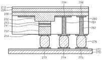
도 2d를 참조하면, 상술한 구조를 다른 기판(270), 예컨대 실리콘 기판(270)과 플립칩 본딩한다. 기판(270) 상에는 실리콘 절연층(272)이 형성되어 있으며, 실리콘 절연층(272) 상에는 p전극(234), 및 금속 포스트들(261)(262)과 각각 대응되는 전극패드들(273,274,275)를 형성한다. 플립칩 본딩을 위해서 인듐 범프(276)를 사용한다. 상기 실리콘 기판(270) 대신에 인쇄회로기판 등이 사용될 수 있다.Referring to FIG. 2D, the above structure is flip-chip bonded to another
플립칩 본딩 후 GaAs 기판(210)을 제거한다. GaAs를 선택적으로 식각하는 용액을 이용하면 GaAs 기판(210)이 제거되고 AlGaAs 식각저지층(212)은 제거되지 않고 남게 된다.After the flip chip bonding, the
도 2e를 참조하면, 식각 저지층(212)와 PD층(220)의 일부를 식각하여 VCSEL의 레이저 광이 출력되는 애퍼처(aperture)(222)를 형성한다. 그리고 식각저지층(212) 및 PD 층(220)에 금속포스트(262)와 대응되는 영역에 관통홀(224)을 형성한다. 이어서, 상기 관통홀(224)을 절연층(226)으로 채운 다음, 상기 절연층(226)을 식각하여 다른 관통홀(미도시)을 형성한다. 이어서, 상기 다른 관통홀을 전극물질을 채워서 PD(220) 상에 전극패드(228)를 형성한다. 이 전극패드(228)는 금속 포스트(262)와 통전된다.Referring to FIG. 2E, an
도 3은 본 발명의 광 송수신 소자의 작동원리를 설명하기 위한 도면이다. 도 2의 구성요소와 실질적으로 동일한 구성요소에는 동일한 참조번호를 사용하고 상세한 설명은 생략한다.3 is a view for explaining the operation principle of the optical transceiver of the present invention. The same reference numerals are used for components substantially the same as those of FIG. 2, and a detailed description thereof will be omitted.
도 3을 참조하면, 본 발명의 광 송수신 소자(200) 상에는 광통신에 사용되는 광 파이버(280)가 배치된다. VCSEL에서 발진한 레이저 광은 애퍼처(222)를 통해 광파이버(280)로 결합(coupling)된다. 일반적으로 VCSEL의 애퍼처(222) 직경(D1)은 10~30um, 광섬유의 코어(core)(282) 직경(D2)은 50~100um 이고 VCSEL 애퍼처(222)와 광섬유 사이의 거리(L)는 50~200um 정도이므로 VCSEL의 레이저 광 대부분이 광섬유로 결합(coupling)되게 된다. 그리고, 광섬유(280)에서 나온 광은 PD(220)에 흡수되는데, PD(220)의 직경(D3)이 대략 50~100um 정도이므로 광섬유(280)와 PD(220) 간의 거리에 따라서 결합(coupling) 효율이 감소할 수 있다. 본 발명에 따른 광 송수신 소자(200)는 광의 입출력이 이루어지는 방향과 전기 신호의 입출력이 이루어지는 방향, 즉 플립칩 본딩 방향이 서로 반대이므로, PD(220)와 광섬유(280) 사이에 본딩 와이어와 같은 방해물이 없다. 따라서, PD(220)와 광섬유(280)를 대략 50um 이내까지 근접시기는 것이 가능하므로, 와이어 본딩 구조에 비해 결합효율이 향상될 것으로 예상된다. 그리고, 광섬유(280)에서 PD(220)로 입사하는 광 중에서 VCSEL 애퍼처(222) 부분에 해당하는 영역은 PD(220)에서 제외된 부분이며, 이는 결합(coupling) 효율을 감소시키는 영향을 주게 된다. 하지만, 전체 PD(220) 면적 중에서 이 애퍼처(222) 부분의 면적은 상당히 작으므로 결합 효율 감소의 영향은 작다고 할 수 있다. 예를 들어, 애퍼처(222)의 직경이 15um, PD(220)의 직경이 70um인 경우 애퍼처(222)가 차지하는 면적은 5% 미만이다.Referring to FIG. 3, an
본 발명에 따르면, 플립 칩 본딩구조를 가지므로, 일반적인 와이어 본딩 구조에서 나타나는 여러 가지 문제점들을 극복할 수 있다. 플립 칩 본딩 구조에서는 와이어 본딩 구조에 비해 전기 배선의 길이가 짧고 wire loop에 의한 인덕턴스(inductance)를 줄일 수 있어서 10 GHz 이상의 고속 data 전송이 가능하다. 그리고, 광의 입출력이 이루어지는 방향과 전기 신호의 입출력이 이루어지는 방향이 서로 반대 방향으로 분리되어 있어서 광 송수신 소자(chip)이 차지하는 공간이 와이어 본딩 방식에 비해 훨씬 간편하다. 따라서, 효율적인 공간 활용이 이루어져서 비용 절감을 기대할 수 있으며, 2차원 배열 형태와 같은 다채널의 VCSEL/PD array의 형성도 용이하다. 또한, 본딩의 내구성이나 신뢰성에 있어서도 와이어 본딩에 비해 훨씬 유리하며, 대량으로 제조 시 양산에 있어서도 유리하다. According to the present invention, since the flip-chip bonding structure is provided, various problems occurring in a general wire bonding structure can be overcome. In the flip-chip bonding structure, the length of the electric wiring is shorter than that of the wire bonding structure, and the inductance due to the wire loop can be reduced, thereby enabling high-speed data transmission of 10 GHz or more. In addition, the direction in which the input / output of light is performed and the direction in which the input / output of the electric signal is performed are separated in opposite directions, so that the space occupied by the optical transceiver is much simpler than the wire bonding method. Therefore, efficient space utilization can be expected and cost reduction can be expected, and it is easy to form a multi-channel VCSEL / PD array such as a two-dimensional array type. In addition, durability and reliability of bonding are much more advantageous than that of wire bonding, and it is advantageous in mass production and mass production.
본 발명에 따르면, LD와 PD를 하나의 소자로 제작함으로써 양방향 광 송수신을 할 수 있으며, 웨이브가이드(waveguide)도 1개만 있으면 되므로 비용 및 공간의 감소를 기대할 수 있다.According to the present invention, bidirectional optical transmission and reception can be performed by fabricating an LD and a PD as a single device, and only one waveguide is required, thereby reducing cost and space.
본 발명은 도면을 참조하여 실시예를 참고로 설명되었으나, 이는 예시적인 것에 불과하며, 당해 분야에서 통상의 지식을 가진 자라면 이로부터 다양한 변형 및 균등한 실시예가 가능하다는 점을 이해할 것이다. 따라서, 본 발명의 진정한 기술적 보호범위는 첨부된 특허청구범위에 한해서 정해져야 할 것이다.While the present invention has been particularly shown and described with reference to exemplary embodiments thereof, it is evident that many alternatives, modifications and variations will be apparent to those skilled in the art. Accordingly, the true scope of the present invention should be determined within the scope of the appended claims.
도 1은 본 발명의 광 송수신 소자를 나타내는 단면도이다.1 is a cross-sectional view showing an optical transmitter / receiver of the present invention.
도 2a 내지 도 2e는 본 발명에 따른 광 송수신 소자의 제조공정을 나타내는 공정도이다.2A to 2E are process drawings showing a manufacturing process of an optical transceiver according to the present invention.
도 3은 본 발명에 의한 광 송수신 소자의 구동방법을 설명하기 위한 도면이다.3 is a view for explaining a driving method of an optical transceiver according to the present invention.
Claims (12)
Translated fromKoreanPriority Applications (2)
| Application Number | Priority Date | Filing Date | Title |
|---|---|---|---|
| KR1020080002640AKR101426285B1 (en) | 2008-01-09 | 2008-01-09 | Optical Transmission / Reception Device and Manufacturing Method Thereof |
| US12/153,650US7656926B2 (en) | 2008-01-09 | 2008-05-22 | Optical connection device and method of fabricating the same |
Applications Claiming Priority (1)
| Application Number | Priority Date | Filing Date | Title |
|---|---|---|---|
| KR1020080002640AKR101426285B1 (en) | 2008-01-09 | 2008-01-09 | Optical Transmission / Reception Device and Manufacturing Method Thereof |
Publications (2)
| Publication Number | Publication Date |
|---|---|
| KR20090076601A KR20090076601A (en) | 2009-07-13 |
| KR101426285B1true KR101426285B1 (en) | 2014-08-05 |
Family
ID=40844510
Family Applications (1)
| Application Number | Title | Priority Date | Filing Date |
|---|---|---|---|
| KR1020080002640AActiveKR101426285B1 (en) | 2008-01-09 | 2008-01-09 | Optical Transmission / Reception Device and Manufacturing Method Thereof |
Country Status (2)
| Country | Link |
|---|---|
| US (1) | US7656926B2 (en) |
| KR (1) | KR101426285B1 (en) |
Families Citing this family (15)
| Publication number | Priority date | Publication date | Assignee | Title |
|---|---|---|---|---|
| JP5659903B2 (en)* | 2011-03-29 | 2015-01-28 | ソニー株式会社 | Light emitting element / light receiving element assembly and manufacturing method thereof |
| US8675706B2 (en)* | 2011-12-24 | 2014-03-18 | Princeton Optronics Inc. | Optical illuminator |
| US9275969B2 (en) | 2012-12-17 | 2016-03-01 | Intel Corporation | Optical interconnect on bumpless build-up layer package |
| KR20140133250A (en)* | 2013-05-10 | 2014-11-19 | 한국전자통신연구원 | distributed feedback laser diode and manufacturing method of the same |
| US9726841B1 (en)* | 2016-07-12 | 2017-08-08 | Inphi Corporation | Integrated photo detector, method of making the same |
| JP6380512B2 (en)* | 2016-11-16 | 2018-08-29 | 富士ゼロックス株式会社 | Light emitting element array and optical transmission device |
| DE102017127920A1 (en) | 2017-01-26 | 2018-07-26 | Taiwan Semiconductor Manufacturing Company, Ltd. | Increased through-hole for connections on different levels |
| US11264780B2 (en)* | 2018-01-26 | 2022-03-01 | Oepic Semiconductors, Inc. | Flip chip backside emitting VCSEL package |
| US10622302B2 (en) | 2018-02-14 | 2020-04-14 | Taiwan Semiconductor Manufacturing Company, Ltd. | Via for semiconductor device connection and methods of forming the same |
| DE102018126130B4 (en) | 2018-06-08 | 2023-08-10 | Taiwan Semiconductor Manufacturing Co., Ltd. | semiconductor device and method |
| US10992100B2 (en) | 2018-07-06 | 2021-04-27 | Taiwan Semiconductor Manufacturing Company, Ltd. | Semiconductor device and method |
| JP7021618B2 (en)* | 2018-08-10 | 2022-02-17 | オムロン株式会社 | Manufacturing method of laser diode array device, laser emission circuit and ranging device |
| TWI701882B (en)* | 2018-11-08 | 2020-08-11 | 晶智達光電股份有限公司 | Laser element |
| CN114498303A (en)* | 2020-11-12 | 2022-05-13 | 常州纵慧芯光半导体科技有限公司 | Laser chip and manufacturing method and application thereof |
| FI130884B1 (en)* | 2021-07-06 | 2024-05-08 | Teknologian Tutkimuskeskus Vtt Oy | Bonding structure |
Citations (3)
| Publication number | Priority date | Publication date | Assignee | Title |
|---|---|---|---|---|
| KR20070061621A (en)* | 2005-12-10 | 2007-06-14 | 한국전자통신연구원 | Optical Transceiver Module |
| KR20070114084A (en)* | 2007-10-09 | 2007-11-29 | 정경희 | Optical module and its manufacturing method |
| KR20080087904A (en)* | 2006-02-28 | 2008-10-01 | 가부시키가이샤후지쿠라 | One-way bidirectional optical module |
Family Cites Families (1)
| Publication number | Priority date | Publication date | Assignee | Title |
|---|---|---|---|---|
| US6780661B1 (en)* | 2000-04-12 | 2004-08-24 | Finisar Corporation | Integration of top-emitting and top-illuminated optoelectronic devices with micro-optic and electronic integrated circuits |
- 2008
- 2008-01-09KRKR1020080002640Apatent/KR101426285B1/enactiveActive
- 2008-05-22USUS12/153,650patent/US7656926B2/enactiveActive
Patent Citations (3)
| Publication number | Priority date | Publication date | Assignee | Title |
|---|---|---|---|---|
| KR20070061621A (en)* | 2005-12-10 | 2007-06-14 | 한국전자통신연구원 | Optical Transceiver Module |
| KR20080087904A (en)* | 2006-02-28 | 2008-10-01 | 가부시키가이샤후지쿠라 | One-way bidirectional optical module |
| KR20070114084A (en)* | 2007-10-09 | 2007-11-29 | 정경희 | Optical module and its manufacturing method |
Also Published As
| Publication number | Publication date |
|---|---|
| KR20090076601A (en) | 2009-07-13 |
| US20090175307A1 (en) | 2009-07-09 |
| US7656926B2 (en) | 2010-02-02 |
Similar Documents
| Publication | Publication Date | Title |
|---|---|---|
| KR101426285B1 (en) | Optical Transmission / Reception Device and Manufacturing Method Thereof | |
| US6597713B2 (en) | Apparatus with an optical functional device having a special wiring electrode and method for fabricating the same | |
| US6953291B2 (en) | Compact package design for vertical cavity surface emitting laser array to optical fiber cable connection | |
| JP3990846B2 (en) | Planar optical element, method for manufacturing the same, and apparatus using the same | |
| US6392256B1 (en) | Closely-spaced VCSEL and photodetector for applications requiring their independent operation | |
| JP2023522559A (en) | 3D and LiDAR sensing module | |
| US7196357B2 (en) | Optical semiconductor apparatus | |
| US7804875B2 (en) | Vertical cavity surface emitting laser module having monitoring photodiode and method of fabricating the same | |
| US8965149B2 (en) | Optoelectronic integrated package module and method of manufacturing the same | |
| EP1919046A2 (en) | Surface-emitting semiconductor array device, module, light source device, data processing apparatus, light transmitting device, light spatial transmitting apparatus, and light spatial tansmitting system | |
| JP2001036197A (en) | Optoelectronic integrated device, method of driving the same, optical wiring system using the device, and arithmetic processing device having the device | |
| JP2000049414A (en) | Optical function element device, optical transmitting / receiving device using the same, optical interconnection device, and optical recording device | |
| EP4062459A1 (en) | High speed and multi-contact leds for data communication | |
| JP3610235B2 (en) | Surface light emitting device | |
| KR100631359B1 (en) | Surface light-emitting type semiconductor laser, light module and light transfer device | |
| JPH1051078A (en) | Semiconductor laser array and method of manufacturing the same | |
| KR20040015283A (en) | Topside active optical device apparatus and method | |
| KR102388885B1 (en) | Optical semiconductor device, optical module and manufacturing method of optical semiconductor device | |
| KR101246137B1 (en) | Light emitting device and optical coupling module | |
| JP2009086539A (en) | Optical module | |
| US20030122142A1 (en) | Submount for vertical cavity surface emitting lasers and detectors | |
| JP2004031455A (en) | Optical interconnection device | |
| KR100327106B1 (en) | Semiconductor laser module | |
| JP4054958B2 (en) | Light emitting device, optical module, display device, optical transmission device | |
| CN119944430A (en) | Package assembly for vertical cavity surface emitting laser on driver IC |
Legal Events
| Date | Code | Title | Description |
|---|---|---|---|
| PA0109 | Patent application | Patent event code:PA01091R01D Comment text:Patent Application Patent event date:20080109 | |
| PG1501 | Laying open of application | ||
| A201 | Request for examination | ||
| PA0201 | Request for examination | Patent event code:PA02012R01D Patent event date:20130109 Comment text:Request for Examination of Application Patent event code:PA02011R01I Patent event date:20080109 Comment text:Patent Application | |
| E902 | Notification of reason for refusal | ||
| PE0902 | Notice of grounds for rejection | Comment text:Notification of reason for refusal Patent event date:20140221 Patent event code:PE09021S01D | |
| E701 | Decision to grant or registration of patent right | ||
| PE0701 | Decision of registration | Patent event code:PE07011S01D Comment text:Decision to Grant Registration Patent event date:20140429 | |
| GRNT | Written decision to grant | ||
| PR0701 | Registration of establishment | Comment text:Registration of Establishment Patent event date:20140729 Patent event code:PR07011E01D | |
| PR1002 | Payment of registration fee | Payment date:20140730 End annual number:3 Start annual number:1 | |
| PG1601 | Publication of registration | ||
| FPAY | Annual fee payment | Payment date:20170630 Year of fee payment:4 | |
| PR1001 | Payment of annual fee | Payment date:20170630 Start annual number:4 End annual number:4 | |
| FPAY | Annual fee payment | Payment date:20180629 Year of fee payment:5 | |
| PR1001 | Payment of annual fee | Payment date:20180629 Start annual number:5 End annual number:5 | |
| PR1001 | Payment of annual fee | Payment date:20200630 Start annual number:7 End annual number:7 | |
| PR1001 | Payment of annual fee | Payment date:20210628 Start annual number:8 End annual number:8 | |
| PR1001 | Payment of annual fee | Payment date:20220622 Start annual number:9 End annual number:9 | |
| PR1001 | Payment of annual fee | Payment date:20230621 Start annual number:10 End annual number:10 | |
| PR1001 | Payment of annual fee | Payment date:20240626 Start annual number:11 End annual number:11 |