KR101421112B1 - Method of manufacturing plasma resistant member by electrostatic slurry spray deposition and method of manufacturing lift pin by the same - Google Patents
Method of manufacturing plasma resistant member by electrostatic slurry spray deposition and method of manufacturing lift pin by the sameDownload PDFInfo
- Publication number
- KR101421112B1 KR101421112B1KR1020120119555AKR20120119555AKR101421112B1KR 101421112 B1KR101421112 B1KR 101421112B1KR 1020120119555 AKR1020120119555 AKR 1020120119555AKR 20120119555 AKR20120119555 AKR 20120119555AKR 101421112 B1KR101421112 B1KR 101421112B1
- Authority
- KR
- South Korea
- Prior art keywords
- alumina
- lift pin
- manufacturing
- wafer
- yttria
- Prior art date
- Legal status (The legal status is an assumption and is not a legal conclusion. Google has not performed a legal analysis and makes no representation as to the accuracy of the status listed.)
- Expired - Fee Related
Links
Images


Classifications
- C—CHEMISTRY; METALLURGY
- C04—CEMENTS; CONCRETE; ARTIFICIAL STONE; CERAMICS; REFRACTORIES
- C04B—LIME, MAGNESIA; SLAG; CEMENTS; COMPOSITIONS THEREOF, e.g. MORTARS, CONCRETE OR LIKE BUILDING MATERIALS; ARTIFICIAL STONE; CERAMICS; REFRACTORIES; TREATMENT OF NATURAL STONE
- C04B35/00—Shaped ceramic products characterised by their composition; Ceramics compositions; Processing powders of inorganic compounds preparatory to the manufacturing of ceramic products
- C04B35/01—Shaped ceramic products characterised by their composition; Ceramics compositions; Processing powders of inorganic compounds preparatory to the manufacturing of ceramic products based on oxide ceramics
- C04B35/10—Shaped ceramic products characterised by their composition; Ceramics compositions; Processing powders of inorganic compounds preparatory to the manufacturing of ceramic products based on oxide ceramics based on aluminium oxide
- C—CHEMISTRY; METALLURGY
- C04—CEMENTS; CONCRETE; ARTIFICIAL STONE; CERAMICS; REFRACTORIES
- C04B—LIME, MAGNESIA; SLAG; CEMENTS; COMPOSITIONS THEREOF, e.g. MORTARS, CONCRETE OR LIKE BUILDING MATERIALS; ARTIFICIAL STONE; CERAMICS; REFRACTORIES; TREATMENT OF NATURAL STONE
- C04B35/00—Shaped ceramic products characterised by their composition; Ceramics compositions; Processing powders of inorganic compounds preparatory to the manufacturing of ceramic products
- C04B35/622—Forming processes; Processing powders of inorganic compounds preparatory to the manufacturing of ceramic products
- C04B35/64—Burning or sintering processes
- C04B35/645—Pressure sintering
- C—CHEMISTRY; METALLURGY
- C04—CEMENTS; CONCRETE; ARTIFICIAL STONE; CERAMICS; REFRACTORIES
- C04B—LIME, MAGNESIA; SLAG; CEMENTS; COMPOSITIONS THEREOF, e.g. MORTARS, CONCRETE OR LIKE BUILDING MATERIALS; ARTIFICIAL STONE; CERAMICS; REFRACTORIES; TREATMENT OF NATURAL STONE
- C04B41/00—After-treatment of mortars, concrete, artificial stone or ceramics; Treatment of natural stone
- C04B41/80—After-treatment of mortars, concrete, artificial stone or ceramics; Treatment of natural stone of only ceramics
- C04B41/81—Coating or impregnation
- C04B41/85—Coating or impregnation with inorganic materials
- C04B41/87—Ceramics
- C—CHEMISTRY; METALLURGY
- C04—CEMENTS; CONCRETE; ARTIFICIAL STONE; CERAMICS; REFRACTORIES
- C04B—LIME, MAGNESIA; SLAG; CEMENTS; COMPOSITIONS THEREOF, e.g. MORTARS, CONCRETE OR LIKE BUILDING MATERIALS; ARTIFICIAL STONE; CERAMICS; REFRACTORIES; TREATMENT OF NATURAL STONE
- C04B2235/00—Aspects relating to ceramic starting mixtures or sintered ceramic products
- C04B2235/02—Composition of constituents of the starting material or of secondary phases of the final product
- C04B2235/30—Constituents and secondary phases not being of a fibrous nature
- C04B2235/32—Metal oxides, mixed metal oxides, or oxide-forming salts thereof, e.g. carbonates, nitrates, (oxy)hydroxides, chlorides
- C04B2235/3217—Aluminum oxide or oxide forming salts thereof, e.g. bauxite, alpha-alumina
- H—ELECTRICITY
- H01—ELECTRIC ELEMENTS
- H01L—SEMICONDUCTOR DEVICES NOT COVERED BY CLASS H10
- H01L21/00—Processes or apparatus adapted for the manufacture or treatment of semiconductor or solid state devices or of parts thereof
- H01L21/02—Manufacture or treatment of semiconductor devices or of parts thereof
- H01L21/02104—Forming layers
- H—ELECTRICITY
- H01—ELECTRIC ELEMENTS
- H01L—SEMICONDUCTOR DEVICES NOT COVERED BY CLASS H10
- H01L21/00—Processes or apparatus adapted for the manufacture or treatment of semiconductor or solid state devices or of parts thereof
- H01L21/02—Manufacture or treatment of semiconductor devices or of parts thereof
- H01L21/04—Manufacture or treatment of semiconductor devices or of parts thereof the devices having potential barriers, e.g. a PN junction, depletion layer or carrier concentration layer
- H01L21/18—Manufacture or treatment of semiconductor devices or of parts thereof the devices having potential barriers, e.g. a PN junction, depletion layer or carrier concentration layer the devices having semiconductor bodies comprising elements of Group IV of the Periodic Table or AIIIBV compounds with or without impurities, e.g. doping materials
- H01L21/30—Treatment of semiconductor bodies using processes or apparatus not provided for in groups H01L21/20 - H01L21/26
- H01L21/302—Treatment of semiconductor bodies using processes or apparatus not provided for in groups H01L21/20 - H01L21/26 to change their surface-physical characteristics or shape, e.g. etching, polishing, cutting
- H01L21/306—Chemical or electrical treatment, e.g. electrolytic etching
- H01L21/3065—Plasma etching; Reactive-ion etching
Landscapes
- Chemical & Material Sciences (AREA)
- Engineering & Computer Science (AREA)
- Ceramic Engineering (AREA)
- Manufacturing & Machinery (AREA)
- Materials Engineering (AREA)
- Structural Engineering (AREA)
- Organic Chemistry (AREA)
- Inorganic Chemistry (AREA)
- Container, Conveyance, Adherence, Positioning, Of Wafer (AREA)
- Drying Of Semiconductors (AREA)
Abstract
Translated fromKoreanDescription
Translated fromKorean본 발명은 정전 분무 슬러리 공정을 이용한 내플라즈마 부재의 제조방법에 관한 것으로서, 더욱 상세하게는 알루미나 성형체에 내플라즈마성이 우수한 세라믹 층을 형성한 후 동시 소성 공정을 진행하여 종래 대기압 플라즈마 용사 코팅막보다 고밀도이고 내플라즈마성이 우수한 내플라즈마 부재를 제조하는 방법 및 이를 이용한 웨이퍼 처리 장치의 리프트 핀을 제조하는 방법에 관한 것이다.More particularly, the present invention relates to a method of manufacturing an internal plasma member using an electrostatic spray slurry process. More particularly, the present invention relates to a method of manufacturing an internal plasma member using an electrostatic spray slurry process, And to a method of manufacturing a lift pin of a wafer processing apparatus using the plasma processing apparatus.
반도체 소자 등과 같은 집적회로 소자의 제조에서는 고밀도 플라즈마 환경의 식각 공정을 수행하므로 내플라즈마 부재를 구비한 식각 장치를 사용한다. 특히, 최근의 반도체 소자 제조용 장비는 소자패턴기술의 미세화로 선폭이 20 nm 이내가 되고, 고밀도 플라즈마 환경에서 사용을 위하여 희토류계 세라믹 재료들을 대기압 플라즈마 용사로 코팅하여 사용하거나 소결용 세라믹 재료를 사용하고 있다. 그러나, 플라즈마에 노출된 반도체 장비 내의 세라믹 및 메탈 부품에서 오염 입자가 발생하여 공정 수율을 감소시키는 것이 반도체 공정의 큰 문제로 대두되고 있고, 향우 반도체 공정의 경우에 웨이퍼 사이즈의 대구경화, 공정의 미세화가 심화될수록 보다 가속화될 것이다.BACKGROUND OF THE INVENTION [0002] In the manufacture of integrated circuit devices such as semiconductor devices, etch processes are performed in a high-density plasma environment, so that an etch apparatus having internal plasma members is used. Particularly, in recent semiconductor device manufacturing equipment, line width is less than 20 nm due to miniaturization of device pattern technology. In order to use in a high density plasma environment, rare earth-based ceramic materials are coated with atmospheric pressure plasma spray or used for sintering ceramic material have. However, the generation of contaminating particles in ceramics and metal parts in semiconductor equipment exposed to plasma has led to a great problem in the semiconductor process. In the case of the sputtering semiconductor process, Will accelerate more.
또한, 반도체 소자 제조에 있어서 실리콘 재질의 웨이퍼(wafer)에 박막을 증착하는 공정을 포함하는데, 상기 박막을 증착하는 공정으로 최근에는 저온에서 상기 박막의 두께를 얇게 하면서 증착률도 우수한 플라즈마 처리 방식이 널리 사용되고 있다. 대표적으로 플라즈마 강화 기상 증착장치(Plasma-Enhanced Chemical Vapor Deposition; 이하, PE-CVD)를 이용하고 있다.The present invention also relates to a process for depositing a thin film on a wafer made of silicon in the manufacture of a semiconductor device. The process for depositing the thin film includes a plasma processing method which has a thin film thickness at a low temperature and a high deposition rate Widely used. Plasma-Enhanced Chemical Vapor Deposition (hereinafter referred to as PE-CVD) is typically used.
상기 PE-CVD 장치는 반응 가스가 주입되는 반응 챔버, 상기 반응 챔버 내에 배치되어 상기 웨이퍼가 놓여지는 서셉터, 상기 반응 가스를 상기 웨이퍼에 균일하게 제공하기 위한 샤워 헤드 및 상기 반응 가스로부터 플라즈마를 형성하기 위하여 고주파 전원(RF)이 인가되는 고주파 전극을 포함한다. 이러한 PE-CVD 장치를 통하여 상기 웨이퍼에 박막을 증착하게 되면, 상기 웨이퍼는 상기 서셉터로부터 분리되어 상기 반응 챔버의 외부로 이송된다. 여기서, 상기 웨이퍼는 상기 서셉터에 수직 방향으로 이동이 가능하도록 삽입된 다수의 리프트 핀들을 통해 상기 서셉터로부터 이격 분리된다.The PE-CVD apparatus includes a reaction chamber into which a reaction gas is injected, a susceptor disposed in the reaction chamber and in which the wafer is placed, a showerhead for uniformly supplying the reaction gas to the wafer, And a high-frequency electrode to which a high-frequency power source RF is applied. When a thin film is deposited on the wafer through the PE-CVD apparatus, the wafer is separated from the susceptor and transferred to the outside of the reaction chamber. Here, the wafer is separated from the susceptor through a plurality of lift pins inserted to be vertically movable to the susceptor.
그러나, 상기 리프트 핀들은 실리콘 재질인 상기 웨이퍼보다 경도가 높은 알루미나(Al2O3) 또는 아노다이징(anodizing) 처리된 알루미늄(Al) 재질로 이루어져 있기 때문에, 공정 진행 시 웨이퍼 뒷면에 스크래치(Scratch) 문제를 야기하는 주원인으로 작용하고 있다. 또한 알루미나(Al2O3) 소재의 경우 공정 시 사용되는 플로린(Fluorine)계 가스와 반응하여 AlFx 부산물(By-product)이 형성되어 웨이퍼 접촉시 웨이퍼 뒷면에 마크(Mark) 스크래치를 남기는 현상을 초래하고 있는 실정이다.However, since the lift pins are made of alumina (Al2 O3 ) or anodized aluminum (Al), which is harder than the wafer made of silicon, a scratch problem As well. In the case of alumina (Al2 O3 ), AlFx by-product is formed by reacting with the fluorine gas used in the process, resulting in a mark scratch on the back side of the wafer during wafer contact .
이러한 마크(Mark) 문제 및 스크래치(Scratch) 현상들은 반도체의 후 공정인 포토(Photo) 공정 진행 시 광학 장비의 정렬(Align)에 영향을 주어 패턴(pattern)에 왜곡(Distortion) 문제를 일으키는 등 공정 시 웨이퍼 수율를 저하시키는 주요 요인으로 작용하고 있다.These mark problems and scratch phenomena affect the alignment of the optical equipment during the photo process, which is the post-process of the semiconductor, to cause a distortion problem in the pattern, Which is a major factor for lowering the wafer yield.
따라서, 본 발명이 해결하고자 하는 과제는 반도체 공정 장비 중 플라즈마 에칭 공정에 사용되고, 반도체 칩의 생산수율에 직접적 영향을 미치는 부품을 알루미나 성형체에 정전 분무 슬러리 증착 공정을 통하여 세라믹층을 코팅한 후 동시 소결 공정을 통하여 우수한 내플라즈마 부재로 제조하는 방법을 제공하는 것이다.Therefore, a problem to be solved by the present invention is to coat a ceramic layer on an alumina compact body through electrostatic spray slurry deposition, which is used in a plasma etching process of a semiconductor process equipment and has a direct effect on the yield of a semiconductor chip, And to provide a method of manufacturing a plasma reactor with excellent plasma resistance.
또한, 상기 내플라즈마 부재의 제조방법을 이용하여 웨이퍼 처리 장치 내의 리프트 핀을 제조하는 방법을 제공하는 것이다.It is another object of the present invention to provide a method of manufacturing a lift pin in a wafer processing apparatus by using the manufacturing method of the inner plasma member.
본 발명은 상기 과제를 해결하기 위하여,In order to solve the above problems,
(a) 세라믹 분말을 포함하는 슬러리 조성물을 제조하는 단계;(a) preparing a slurry composition comprising a ceramic powder;
(b) 상기 슬러리 조성물을 알루미나 가압 성형체 상에 정전 분무 방법으로 분무하여 세라믹 층을 코팅하는 단계; 및(b) spraying the slurry composition onto an alumina pressed body by electrostatic spraying to coat the ceramic layer; And
(c) 상기 세라믹 층이 코팅된 알루미나 가압 성형체를 동시 소결하는 단계;를 포함하는 내플라즈마 부재의 제조방법을 제공한다.(c) co-sintering the alumina press-molded body coated with the ceramic layer.
본 발명의 일 실시예에 의하면, 상기 세라믹 분말은 이트리아(Y2O3), 지르코니아(ZrO2), YSZ(yittria stabilized zirconia), 실리콘 카바이드(SiC), 질화 규소(Si3N4) 및 질화 알루미늄(AlN) 중에서 선택되는 1종 이상일 수 있다.According to one embodiment of the invention, the ceramic powder is yttria (Y2 O3), zirconia(ZrO 2), YSZ (yittria stabilized zirconia), silicon carbide (SiC), silicon nitride (Si3 N4), and And aluminum nitride (AlN).
본 발명의 다른 일 실시예에 의하면, 상기 슬러리 조성물은 알콜과 유기 용매의 혼합 용매와 상기 세라믹 분말과 폴리비닐부티랄을 혼합하여 제조한 것일 수 있다.According to another embodiment of the present invention, the slurry composition may be prepared by mixing a mixed solvent of an alcohol and an organic solvent with the ceramic powder and polyvinyl butyral.
본 발명의 다른 일 실시예에 의하면, 상기 정전 분무 방법은 상기 슬러리 조성물을 시린지 펌프를 이용하여 노즐로 이송한 후 분문하여 수행할 수 있으며, 상기 슬러리 유량은 1-20 mL/h으로 하고, 상기 알루미나 가압 성형체와 노즐간의 이격거리는 2-15 cm이며, 증착 시간은 5-100 분이고, 인가 전압은 2-20 kV일 수 있다.According to another embodiment of the present invention, the electrostatic spraying method may be performed by transferring the slurry composition to a nozzle using a syringe pump and pulverizing the slurry composition. The flow rate of the slurry may be 1-20 mL / h, The separation distance between the alumina pressed body and the nozzle is 2-15 cm, the deposition time is 5-100 minutes, and the applied voltage may be 2-20 kV.
본 발명의 다른 일 실시예에 의하면, 상기 세라믹 층과 알루미나 가압 성형체를 동시 소결하는 온도는 1600-1700 ℃일 수 있다.According to another embodiment of the present invention, the temperature for co-sintering the ceramic layer and alumina press-molded body may be 1600-1700 ° C.
본 발명의 다른 일 실시예에 의하면, 상기 알루미나 가압 성형체는 80-90 ㎛ 크기의 알루미나 분말을 30-50 MPa의 압력으로 가압 프레스하여 제조할 수 있다.According to another embodiment of the present invention, the alumina press-molded body can be produced by press-pressing alumina powder having a size of 80-90 mu m at a pressure of 30-50 MPa.
본 발명의 다른 일 실시예에 의하면, 상기 세라믹 분말은 입자 크기가 10 nm - 1 ㎛일 수 있다.
According to another embodiment of the present invention, the ceramic powder may have a particle size of 10 nm - 1 탆.
본 발명은 상기 내플라즈마 부재의 제조방법을 이용한 리프트 핀의 제조방법에 있어서, 상기 내플라즈마 부재는 웨이퍼 처리 장치의 리프트 핀이고, 상기 (a) 단계의 알루미나 가압 성형체는 상기 리프트 핀의 몸통부이며, 상기 (b) 단계에서 코팅되는 세라믹 층은 웨이퍼를 지지하는 리프트 핀 상부에만 코팅되는 것을 특징으로 하는 리프트 핀의 제조방법을 제공한다.In the method of manufacturing a lift pin using the method of manufacturing the plasma member, the inner plasma member is a lift pin of the wafer processing apparatus, and the alumina press-molded body of the step (a) And the ceramic layer coated in the step (b) is coated only on the upper part of the lift pin supporting the wafer.
또한, 본 발명은 상기 제조방법에 따라 제조된 리프트 핀 및 이를 포함하는 웨이퍼 처리 장치를 제공한다.The present invention also provides a lift pin manufactured according to the above manufacturing method and a wafer processing apparatus including the lift pin.
본 발명에 따르면 정전 분무 슬러리 증착 공정에 의해서 내플라즈마성이 우수한 이트리아 등의 세라믹 소결체를 제공할 수 있어 고밀도 플라즈마 공정이 요구되는 반도체 공정 장비의 부품에 활용할 수 있다.According to the present invention, ceramic sintered bodies such as yttria having excellent plasma resistance can be provided by the electrostatic spray slurry deposition process, and the present invention can be applied to parts of semiconductor processing equipment requiring a high-density plasma process.
또한, 본 발명에 따라 코팅된 세라믹 층은 세라믹 소결체로서의 물성을 나타내므로 종래 세라믹 층을 대기압 플라즈마 용사 코팅으로 형성시 세라믹 분말이 모재에 충돌하면서 발생되는 기공에 의한 파티클 발생과 아킹으로 인한 문제점을 해결할 수 있다.In addition, since the ceramic layer coated according to the present invention exhibits physical properties as a ceramic sintered body, when the conventional ceramic layer is formed by atmospheric pressure plasma spray coating, problems caused by particle generation and arcing due to pores generated when ceramic powder collides with the base material are solved .
또한, 알루미나 소결체를 완제품으로 가공한 후에 대기압 플라즈마 용사 코팅을 진행하는 것이 아니라 알루미나 성형체 상태에서 세라믹 층을 증착한 후에 동시 소결하여 이종 세라믹 소결체를 형성하므로 공정이 간단하고 공정 비용이 저렴한 장점을 갖는다.Further, the present invention is advantageous in that the process is simple and the process cost is low, since the sintered alumina is processed into a finished product and then the atmospheric plasma spray coating is not performed but the ceramic layer is deposited in the form of an alumina compact and simultaneously sintered to form a heterogeneous ceramic sintered body.
또한, 종래의 대기압 플라즈마 용사 코팅법에 비하여 증착층의 수명이 연장되고, 파티클 제어, 수율 향상, 희토류 저감 등의 효과를 가져올 수 있다.Further, the lifetime of the vapor deposition layer is prolonged as compared with the conventional atmospheric pressure plasma spray coating method, and the effect of particle control, yield improvement, rare earth reduction and the like can be brought about.
또한, 본 발명에 따라 제조된 웨이퍼 처리 장치의 리프트 핀은 종래 몸통부와 웨이퍼 지지부를 각각 체결하거나 접합하여 제조한 것이 아니라 몸통부 상에 세라믹 층인 웨이퍼 지지부를 증착하여 일체형으로 제조하여 지지부의 탈리를 방지할 수 있고, 지지부가 웨이퍼보다 경도가 낮은 세라믹 층으로 코팅되어 있어 웨이퍼에 가해지는 손상을 방지할 수 있다.In addition, the lift pins of the wafer processing apparatus manufactured according to the present invention are not manufactured by fastening or bonding the conventional body portion and the wafer supporting portion, but are manufactured by integrally manufacturing the wafer supporting portions, which are ceramic layers, on the body portion, And the support portion is coated with a ceramic layer having a hardness lower than that of the wafer, so that damage to the wafer can be prevented.
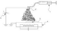
도 1은 본 발명에 따른 내플라즈마 부재의 제조방법을 적용하기 위하여 구현된 정전 분무 슬러리 증착 공정 장비를 나타낸 개념도이다.
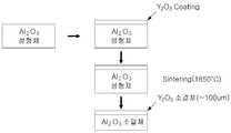
도 2는 본 발명에 따른 내플라즈마 부재의 제조공정 순서도이다.
도 3은 본 발명에 따른 내플라즈마 부재의 제조공정에 따른 증착 구조를 나타낸 개념도이다.
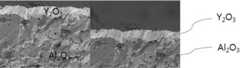
도 4는 본 발명의 일 실시예에 따라 이트리아 소결체가 증착된 알루미나 소결체(이종 세라믹 소결체)의 단면에 대한 주사전자현미경 사진이다.
도 5는 본 발명에 따라 제조된 내플라즈마 부재에 대한 부식특성을 평가한 결과를 나타낸 그래프이다.
도 6은 본 발명의 내플라즈마 부재의 제조방법에 의해서 제조될 수 있는 웨이퍼 처리 장치 내의 리프트 핀 및 이를 포함하는 웨이퍼 처리 장치의 구조도이다.
도 7은 본 발명에 따른 리프트 핀의 제조공정 순서도이다.
도 8은 본 발명에 따라 제조된 리프트 핀의 나타낸 개념도이다.FIG. 1 is a conceptual diagram showing an electrostatic spray slurry deposition processing apparatus implemented to apply the method of manufacturing a plasma member according to the present invention.
Fig. 2 is a flow chart of the manufacturing process of the inner plasma member according to the present invention.
3 is a conceptual view showing a deposition structure according to a manufacturing process of an inner plasma member according to the present invention.
4 is a scanning electron micrograph of an alumina sintered body (heterogeneous ceramic sintered body) on which an yttria sintered body is deposited according to an embodiment of the present invention.
5 is a graph showing a result of evaluating corrosion characteristics of an inner plasma member manufactured according to the present invention.
6 is a structural view of a lift pin and a wafer processing apparatus including the lift pin in a wafer processing apparatus that can be manufactured by the method of manufacturing an inner plasma member of the present invention.
7 is a flowchart of a manufacturing process of a lift pin according to the present invention.
8 is a conceptual view showing a lift pin manufactured according to the present invention.
이하, 본 발명을 더욱 상세하게 설명한다.Hereinafter, the present invention will be described in more detail.
본 발명은 정전 분무 슬러리 증착 공정을 이용하여 반도체 공정 장비 중 에칭 공정에 사용되는 부품을 제조하는 방법에 관한 것으로서, 알루미나 성형체에 내플라즈마성이 우수한 세라믹 층을 코팅한 후에 동시 소성을 진행하여 고밀도의 이종 세라믹 소결체를 제조하는 것을 특징으로 한다.The present invention relates to a method of manufacturing components used in an etching process in semiconductor processing equipment using an electrostatic spray slurry deposition process, in which a ceramic layer having excellent plasma resistance is coated on an alumina compact, Thereby producing a heterogeneous ceramic sintered body.
즉, 알루미나 가압 성형체를 제조하고, 알루미나와 상이한 이종의 세라믹을 정전 분무 슬러리 공정으로 증착한 후에 동시 소성을 진행하여 알루미나 소결체 상에 이트리아 소결체가 고밀도로 형성된 이종 세라믹체를 제조한다.That is, an alumina press molded product is prepared, a heterogeneous ceramic different from alumina is deposited by an electrostatic spray slurry process, and co-firing is carried out to produce a heterogeneous ceramic body in which the yttria sintered body is formed at high density on the alumina sintered body.
본 발명에 따른 내플라즈마 부재의 제조방법은 하기의 단계를 포함하는 것을 특징으로 한다.A method of manufacturing an inner plasma member according to the present invention includes the following steps.
(a) 세라믹 분말을 포함하는 슬러리 조성물을 제조하는 단계,(a) preparing a slurry composition comprising a ceramic powder,
(b) 상기 슬러리 조성물을 알루미나 가압 성형체 상에 정전 분무 방법으로 분무하여 세라믹 층을 코팅하는 단계,(b) spraying the slurry composition onto an alumina pressed body by an electrostatic spraying method to coat the ceramic layer,
(c) 상기 세라믹 층이 코팅된 알루미나 가압 성형체를 동시 소결하는 단계.(c) simultaneously sintering the alumina press-molded body coated with the ceramic layer.
상기 (a) 단계에서 제조되는 슬러리 조성물은 이후 정전 분무 과정에서 액적의 크기를 보다 작게 하여 치밀한 세라믹 층을 형성하기 위하여, 우수한 분산성 확보가 요구된다. 따라서, 세라믹 분말을 유기 용매에 분산시 바인더 및 분산제의 역할을 동시에 수행하는 폴리비닐부티랄을 첨가하여 혼합한다.The slurry composition prepared in the step (a) is required to have good dispersibility in order to form a dense ceramic layer by reducing the size of droplets in the electrostatic spraying process. Therefore, when the ceramic powder is dispersed in an organic solvent, polyvinyl butyral, which simultaneously acts as a binder and a dispersant, is added and mixed.
또한, 이후 소결과정에서 빠른 휘발을 위하여 유기용매에 일정비로 알콜이 혼합된 혼합용매를 사용한다. 알콜로는 메탄올, 에탄올, 프로판올, 부탄올 등의 저급 알콜을 사용하고, 유기용매로는 폴리비닐부티랄의 용해를 위하여 톨루엔, 벤젠, 클로로포름, 테트라하이드로퓨란, 에틸렌글리콜, 디에틸렌글리콜, 에틸에테르아세테이트, 벤질알코올 등을 사용하고, 혼합비는 유기용매와 알콜을 7:3으로 혼합하는 것이 바람직하다.Also, for rapid volatilization in the subsequent sintering process, a mixed solvent in which alcohol is mixed with organic solvent at a certain ratio is used. Examples of the alcohol include lower alcohols such as methanol, ethanol, propanol and butanol, and organic solvents include toluene, benzene, chloroform, tetrahydrofuran, ethylene glycol, diethylene glycol, ethyl ether acetate , Benzyl alcohol and the like are used, and it is preferable to mix an organic solvent and an alcohol at a mixing ratio of 7: 3.
상기 (b) 단계에서 정전 분무 방법으로 알루미나 가압체에 세라믹층을 코팅하는 방법은 하기 도 1에 나타낸 장치를 이용한다.A method of coating the ceramic layer on the alumina press body by the electrostatic spraying method in the step (b) is as shown in FIG.
알루미나 가압 성형체를 기판 홀더(3)에 장착하고, 상기 슬러리 조성물을 시린지 펌프(1)에 투입한 후, 시린지 펌프(1)에 연결된 노즐(2)을 사용하고, 전압 인가 장치(5)를 이용하여 고전압을 인가하여 상기 슬러리 조성물을 액적 형태로 분무하여 알루미나 가압 성형체 상에 세라믹층을 형성한다.The slurry composition is put into the syringe pump 1 and then the nozzle 2 connected to the syringe pump 1 is used and the
이때, 상기 슬러리 유량은 1-20 mL/h으로 하고, 상기 알루미나 가압 성형체와 노즐간의 이격거리는 2-15 cm로 하고, 증착 시간은 5-100 분이고, 인가 전압은 2-20 kV로 하여 수행한다.
At this time, the slurry flow rate is set to 1-20 mL / h, the distance between the alumina press molded body and the nozzle is 2-15 cm, the deposition time is 5-100 minutes, and the applied voltage is 2-20 kV .
상기 (c) 단계에서 세라믹이 코팅된 알루미나 가압 성형체의 동시 소결온도는 1600-1700 ℃일 수 있고, 보다 바람직하게는 1650 ℃일 수 있다. 1600 ℃ 이하인 경우에는 세라믹층이 충분한 밀도를 보여주지 못하고 알루미나 소결체와의 계면에서 분리되는 현상이 발생한다. 또한, 1700 ℃ 이상인 경우에는 입성장이 과하게 진행되어 강도값이 떨어지고 수축율을 제어하기가 곤란한 문제점이 발생한다.
The simultaneous sintering temperature of the ceramic-coated alumina press-molded body in the step (c) may be 1600-1700 ° C, more preferably 1650 ° C. When the temperature is lower than 1600 DEG C, the ceramic layer does not exhibit a sufficient density and is separated from the interface with the alumina sintered body. If the temperature is higher than 1700 占 폚, there is a problem that the grain growth is excessively advanced, the strength value is lowered and it is difficult to control the shrinkage ratio.
본 발명에 있어서, 세라믹 분말은 이트리아(Y2O3), 지르코니아(ZrO2), YSZ(yittria stabilized zirconia), 실리콘 카바이드(SiC), 질화 규소(Si3N4) 및 질화 알루미늄(AlN) 중에서 선택되는 1종 이상일 수 있으며, 입자 크기는 10 nm - 1 ㎛일 수 있다. 10 nm 보다 작은 경우에는 분산이 용이하지 않으며, 1 ㎛ 이상일 경우에는 세라믹 층 코팅 후에 동시소결시 알루미나 가압 성형체와 세라믹 층의 계면에서 입성장 차이 속도에 따라 계면 분리 현상이 심해진다.
In the present invention, the ceramic powder is selected from the group consisting of yttria (Y2 O3 ), zirconia (ZrO2 ), yttria stabilized zirconia, silicon carbide (SiC), silicon nitride (Si3 N4 ) And the particle size may be 10 nm - 1 占 퐉. When the thickness is less than 10 nm, the dispersion is not easy. If the thickness is more than 1 탆, the interface separation phenomenon becomes more severe at the interface between the alumina pressed body and the ceramic layer due to the difference in the grain growth rate during simultaneous sintering after the ceramic layer coating.
본 발명은 상기 내플라즈마 부재의 제조방법에 있어서, 상기 내플라즈마 부재가 리프트 핀인 것을 특징으로 하는 내플라즈마 부재의 제조방법을 제공한다.The present invention provides a method of manufacturing an inner plasma member characterized in that the inner plasma member is a lift pin.
즉, 본 발명은 상기 내플라즈마 부재의 제조방법에 있어서, 상기 내플라즈마 부재는 웨이퍼 처리 장치의 리프트 핀이고, 상기 (a) 단계의 알루미나 가압 성형체는 상기 리프트 핀의 몸통부이며, 상기 (b) 단계에서 코팅되는 세라믹 층은 웨이퍼를 지지하는 리프트 핀 상부에만 코팅되는 것을 특징으로 하는 내플라즈마 부재의 제조방법을 제공한다.That is, in the method of manufacturing the inner plasma member, the inner plasma member is a lift pin of the wafer processing apparatus, the alumina press-molded body of the step (a) is the body portion of the lift pin, Wherein the ceramic layer to be coated in the step is coated only on the upper portion of the lift pin supporting the wafer.
웨이퍼 처리장치를 통하여 웨이퍼에 박막을 증착하게 되면, 웨이퍼는 서셉터로부터 분리되어 여러 반응 챔버의 외부로 이송된다. 여기서 증착된 웨이퍼는 장비 내 수직 방향으로 이동이 가능하도록 삽입된 다수의 리프트 핀들을 통해서 서셉터로부터 이격 분리된다.When a thin film is deposited on the wafer through the wafer processing apparatus, the wafer is separated from the susceptor and transferred to the outside of the various reaction chambers. Wherein the deposited wafer is separated from the susceptor through a plurality of lift pins inserted therein for vertical movement in the apparatus.
일반적으로 상기 리프트 핀들은 실리콘 재질인 상기 웨이퍼보다 경도가 높은 알루미나 또는 아노다이징(anodizing) 처리된 알루미늄(Al) 재질로 이루어져 있기 때문에, 상기 웨이퍼를 지지하는 지지면에 스크래치(scratch) 불량을 발생시킬 수 있는 문제점이 있다.Generally, since the lift pins are made of alumina or anodized aluminum (Al) material having a hardness higher than that of the wafer made of a silicon material, it is possible to cause a scratch defect on a supporting surface for supporting the wafer There is a problem.
따라서, 리프트 핀에서 웨이퍼를 지지하는 부분만을 따라 실리콘 웨이퍼보다 경도가 낮은 세라믹 물질로 제작하여 리프트 핀의 몸통부에 체결하거나 접착하는 방식으로 개선하고 있으나, 세라믹층이 탈리되는 문제점이 여전히 있다.Therefore, although the lift pin is made of a ceramic material having a hardness lower than that of the silicon wafer only by the portion supporting the wafer, the lift pin is fastened or bonded to the body of the lift pin, but the ceramic layer is still detached.
본 발명은 리프트 핀의 몸통부와 그 위의 웨이퍼 지지부에 세라믹층이 코팅된 리프트 핀을 일체형으로 제조할 수 있어 상기와 같은 문제점을 해결할 수 있다.
The present invention can solve the above problems by integrally manufacturing a lift pin coated with a ceramic layer on the body portion of the lift pin and the wafer supporting portion thereon.
이하, 바람직한 실시예를 들어 본 발명을 더욱 상세하게 설명한다. 그러나, 이들 실시예는 본 발명을 보다 구체적으로 설명하기 위한 것으로, 본 발명의 범위가 이에 의하여 제한되지 않고, 본 발명의 범주 및 기술사상 범위 내에서 다양한 변경 및 수정이 가능함은 당업계의 통상의 지식을 가진 자에게 자명할 것이다.
Hereinafter, the present invention will be described in more detail with reference to preferred embodiments. It will be understood by those skilled in the art that various changes in form and details may be made therein without departing from the spirit and scope of the invention as defined by the appended claims. It will be clear to those who have knowledge.
<실시예><Examples>
실시예 1. 이트리아가 코팅된 내플라즈마 부재의 제조Example 1. Preparation of yttria coated inner plasma member
(1) 이트리아 나노 분말 슬러리의 제조(1) Preparation of yttrian powder slurry
슬러리 혼합기 내부에 이소프로필 알콜/톨루엔(7:3) 50 mL, 폴리비닐부티랄(PVB) 0.2 g을 첨가하여 300 분 동안 혼합시켰다. 이후, 폴리비닐부티랄이 용매에 잘 용해된 상태에서 50 nm 크기의 이트리아 나노분말 4 g을 첨가하고, 마그네틱 바를 이용하여 균일하게 혼합하여 이트리아 나노 분말 슬러리를 제조하였다.
50 mL of isopropyl alcohol / toluene (7: 3) and 0.2 g of polyvinyl butyral (PVB) were added into the slurry mixer and mixed for 300 minutes. Thereafter, 4 g of yttria nanoparticles having a size of 50 nm was added in a state where the polyvinyl butyral was well dissolved in a solvent, and the mixture was homogeneously mixed using a magnetic bar to prepare an yttrian powder slurry.
(2) 알루미나 성형체 제조(2) Production of alumina compacted body
순도 99.7% 이상, 평균입도는 80-90 ㎛인 알루미나 분말을 30 mm 금형몰드에 5 g을 칭량하여 장입한 후 일축가압 프레스를 이용하여 약 40 MPa의 압력을 가하여 알루미나 성형체를 제조하였다.
Alumina powders having a purity of 99.7% or more and an average particle size of 80-90 μm were weighed into a mold of 30 mm mold and weighed, and a pressure of about 40 MPa was applied using a uniaxial pressing press to produce an alumina compact.
(3) 정전분무 슬러리 증착 공정을 이용한 알루미나 성형체 상에 이트리아 증착(3) Yttria deposition on an alumina compact using an electrostatic spray slurry deposition process
상기 이트리아 나노 분말 슬러리를 시린지 펌프를 이용하여 내경 0.03 mm 및 외경 0.64 mm 스테인리스 노즐로 이송하였고, 시린지 펌프로부터의 슬러리 공급 유량을 10 mL/h로 공급하고, 이때 노즐에 인가된 DC 전압은 12 kV, 알루미나 성형체와 노즐 거리는 7 cm로 유지하였다. 이때 알루미나 성형체에 증착하는 시간은 30 분으로 고정하여 분사하였다.
The yttria powder slurry was transferred to a stainless steel nozzle having an inner diameter of 0.03 mm and an outer diameter of 0.64 mm using a syringe pump, and a slurry supply flow rate of 10 mL / h was supplied from the syringe pump. The DC voltage applied to the nozzle was 12 kV, the distance between the alumina compact and the nozzle was maintained at 7 cm. At this time, the deposition time of the alumina compact was fixed to 30 minutes.
(4) 알루미나 성형체 및 이트리아 층의 동시 소결(4) simultaneous sintering of alumina compact and yttria layer
알루미나 성형체에 정전분무 슬러리 증착 공정을 통하여 이트리아 나노 분말 슬러리를 증착한 후, 일반 대기 분위기 산화로를 이용하여 1650 ℃에서 2 시간 동안 동시소결을 진행하여 알루미나 소결체 위에 계면이 보이지 않는 안정적인 이트리아 소결체인 이종 세라믹을 제조하였다.
The yttria powder slurry was deposited on the alumina compact by electrostatic spray slurry deposition and then sintered at 1650 ° C for 2 hours using a normal atmospheric oxidation furnace to obtain a stable yttria sintered body having no interface on the alumina sintered body Were prepared.
실시예 2 내지 6.Examples 2-6.
상기 실시예 1과 동일한 방법으로 제조하고, 다만 상기 실시예 1-(3) 및 1-(4)에서의 증착 시간과 소결온도를 달리하여 제조하였고, 증착시간 및 소결온도는 하기 [표 1]에 나타내었다.
The sintering time and sintering temperature were determined in the same manner as in Example 1, except that the deposition time and sintering temperature in Examples 1- (3) and 1- (4) Respectively.
비교예 1 내지 4.Comparative Examples 1 to 4.
상기 실시예 1과 동일한 방법으로 제조하고, 다만 1.5 ㎛ 크기의 이트리아 나노 분말을 사용하였으며, 상기 실시예 1-(3) 및 1-(4)에서의 증착 시간과 소결온도를 달리하여 제조하였고, 증착시간 및 소결온도는 하기 [표 1]에 나타내었다.
Was prepared in the same manner as in Example 1, except that yttria powder having a size of 1.5 탆 was used. The sintering time and sintering temperature were different in Examples 1- (3) and 1- (4) , The deposition time and the sintering temperature are shown in Table 1 below.
실험예 1.Experimental Example 1
상기 실시예 1 내지 6 및 비교예 1 내지 4에 따라 제조된 내플라즈마 부재(이종 세라믹)에 대해서 주사전자현미경 사진으로 파단면을 확인하여 계면 상태를 분석하였고, 그 결과를 하기 [표 1]에 나타내었다.
The interfacial states of the inner plasma member (heterogeneous ceramic) produced according to Examples 1 to 6 and Comparative Examples 1 to 4 were analyzed by scanning electron microscopy to analyze the interfacial states. The results are shown in Table 1 below Respectively.
실험예 2.Experimental Example 2
상기 실시예 1 내지 6 및 비교예 1 내지 4에 따라 제조된 내플라즈마 부재(이종 세라믹)에 대해서 소결 후의 상대 밀도 및 수축율을 조사하였고, 그 결과를 하기 [표 1]에 나타내었다. 밀도의 측정 방법은 일반적인 방법인 아르키메데스 방법을 사용하였고 수축율의 경우에는 성형체 상태에서의 사이즈(두께, 길이 등) 측정치와 소결한 후의 측정치를 비교하여 그 결과를 나타내었다.The relative density and shrinkage ratio after sintering were measured for the inner plasma member (heterogeneous ceramic) produced according to Examples 1 to 6 and Comparative Examples 1 to 4, and the results are shown in Table 1 below. The density was measured by the Archimedes method. The shrinkage ratio was compared with the measured size (thickness, length, etc.) and the measured value after sintering.
입자크기Y2 O3
Particle size
(mL/h)flux
(mL / h)
(cm)Separation distance
(cm)
(분)Deposition time
(minute)
/
시간
(℃/h)Sintering temperature
/
time
(° C / h)
상태Interface
condition
(%)Contraction ratio
(%)
밀도
(%)opponent
density
(%)
현상
없음detach
phenomenon
none
분리slightly
detach
분리slightly
detach
현상
없음detach
phenomenon
none
현상
없음detach
phenomenon
none
현상
없음detach
phenomenon
none
하기 도 4는 상기 실시예 1에 따라 정전분무 슬러리 증착 공정을 통하여 제조된 알루미나 소결체 위에 증착된 이트리아 소결체의 단면에 대한 주사전자현미경 사진이다.4 is a scanning electron microscope (SEM) image of the cross section of the yttria sintered body deposited on the alumina sintered body manufactured through the electrostatic spray slurry deposition process according to the first embodiment.
하기 도 4는 상기 실시예 1에 따른 소결체의 미세구조를 보여주는 것으로서, 좌측 이미지는 소결체의 중앙부, 우축 이미지는 소결체의 가장자리에 대한 파단면을 보여주는 것으로서, 하기 도 4를 참조하면 알루미나 소결체 상에 이트리아 층이 안정적으로 증착되어 계면분리 현상 없이 접합강도가 우수한 이종 세라믹(알루미나/이트리아)이 형성되었음을 알 수 있다. 또한, 밀도 및 수축율에 있어서 상대밀도 99% 이상을 보여주고, 수축율 역시 15-16%을 나타내었다.
4 shows the microstructure of the sintered body according to the first embodiment. The left side image shows the center part of the sintered body, and the right axis image shows the fractured surface with respect to the edge of the sintered body. Referring to FIG. 4, (Alumina / yttria) was formed with good bonding strength without interfacial separation phenomenon. The density and shrinkage showed a relative density of more than 99%, and the shrinkage rate was 15-16%.
실험예 3.Experimental Example 3.
상기 실시예 1(본 발명에 따른 이트리아 소결체, 시료 2), 이트리아 벌크(bulk) 소결체(시료 1), 대기압 플라즈마로 코팅된 이트리아(시료 3), 알루미나 벌크 소결체(시료 4), 대기압 플라즈마로 코팅된 알루미나(시료 5), 실리콘 카바이드(SiC)(시료 6) 및 석영(시료 7)에 대해서 플라즈마 장비를 이용하여 가스 flow rate를 CF4/Ar/O2=100/100/10 sccm으로 하고 RF power 1500 W에서 에칭 테스트를 실시한 결과를 하기 도 5에 나타내었다. 하기 도 5를 참조하면 본 발명에 따른 이트리아 소결체의 경우 이트리아 벌크 소결체와 거의 동일한 두께를 나타내었다. 즉, 내플라즈마성이 가장 우수한 이트리아 벌크 소결체와 동일한 효과를 나타냄을 알 수 있다.(Yttria sintered body according to the present invention, sample 2), yttria bulk sintered body (sample 1), yttria coated with atmospheric pressure plasma (sample 3), alumina bulk sintered body (sample 4) Plasma-coated alumina (Sample 5), Silicon Carbide (SiC) (Sample 6) and Quartz (Sample 7) were subjected to gas flow rate CF4 / Ar / O2 = 100/100/10 sccm And an etching test was carried out at 1500 W of RF power. The results are shown in FIG. Referring to FIG. 5, the yttria sintered body according to the present invention has substantially the same thickness as the yttria bulk sintered body. That is, it can be seen that the same effects as those of the yttria bulk sintered body having the best plasma resistance are exhibited.
시료 2는 본 발명의 실시예 1에 따른 것이고, 나머지 시료 1, 3, 4, 5, 6, 7 모두 현재 반도체 공정 중에 사용되고 있는 제품을 구하여 테스트 시편에 맞게 가공하였다.Sample 2 was according to Example 1 of the present invention, and the remaining
구체적으로 시료 1은 이트리아 분말을 이용하여 일축가압 또는 CIP 성형 후 1650 ℃에서 소결한 이트리아 소결체이고, 시료 3은 대기압 플라즈마로 코팅된 이트리아로서, 알루미나 소결체 위에 내플라즈마성이 우수한 이트리아 분말을 대기압에서 플라즈마 건에 용사용 분말로 제조된 이트리아 분말을 투입하여 대기압에서 녹인 후 분사하여 코팅한 제품이며, 시료 4는 알루미나 분말을 이용하여 일축가압 또는 CIP 성형한 후 1650 ℃에서 소결한 알루미나 소결체이고, 시료 5는 대기압 플라즈마로 코팅된 알루미나로서, 알루미나 소결체 위에 알루미나 분말을 대기압에서 플라즈마 건에 용사용 분말로 제조된 알루미나 분말을 투입하여 대기압에서 녹인 후 분사하여 코팅한 제품이고, 시료 6은 실리콘 카바이드 분말을 이용해서 일축가압 또는 1800 ℃에서 반응소결을 이용하여 소결한 실리콘 카바이드 제품이며, 시료 7은 쿼츠(석영)이다.
Specifically, Sample 1 is a yttria sintered body obtained by sintering at 1650 ° C. after uniaxial pressing or CIP molding using yttria powder.
실시예 7. 웨이퍼가 접촉하는 웨이퍼 지지 부분에 이트리아가 코팅된 리프트 핀의 제조Example 7. Manufacture of yttria-coated lift pins on a wafer support portion where the wafer contacts
(1) 이트리아 나노 분말 슬러리의 제조(1) Preparation of yttrian powder slurry
슬러리 혼합기 내부에 이소프로필 알콜/톨루엔(7:3) 50 mL, 폴리비닐부티랄(PVB) 0.2 g을 첨가하여 300 분 동안 혼합시켰다. 이후, 폴리비닐부티랄이 용매에 잘 용해된 상태에서 50 nm 크기의 이트리아 나노분말 4 g을 첨가하고, 마그네틱 바를 이용하여 균일하게 혼합하여 이트리아 나노 분말 슬러리를 제조하였다.
50 mL of isopropyl alcohol / toluene (7: 3) and 0.2 g of polyvinyl butyral (PVB) were added into the slurry mixer and mixed for 300 minutes. Thereafter, 4 g of yttria nanoparticles having a size of 50 nm was added in a state where the polyvinyl butyral was well dissolved in a solvent, and the mixture was homogeneously mixed using a magnetic bar to prepare an yttrian powder slurry.
(2) 알루미나 리프트 핀 성형체의 제조(2) Production of Alumina Lift Pin Molded Body
리프트 핀은 현재 반도체 장비 내에서 사용되고 있는 것과 동일하게 순도 99.7% 이상의 알루미나 분말을 이용하여 제조하였으며, 성형체의 사이즈는 100 mm × 20 Φ로 제조하였다.
The lift pins were manufactured using alumina powders having a purity of 99.7% or more as in the current semiconductor equipment, and the size of the formed bodies was 100 mm × 20 Φ.
(3) 정전분무 슬러리 증착 공정(3) Electrostatic spray slurry deposition process
상기 알루미나 리프트 핀 성형체의 웨이퍼 지지면 부위를 마스킹 하여 지지면 부위에만 이트리아 나노분말 슬러리 조성물을 시린지 펌프를 이용하여 내경 0.03 mm 및 외경 0.64 mm 스테인리스 노즐로 이송하였고, 시린지 펌프로부터의 슬러리 공급 유량을 10 mL/h로 공급하고, 이때 노즐에 인가된 DC 전압은 12 kV, 알루미나 리프트 핀 성형체와 노즐 거리는 7 cm로 유지하였다. 이때, 알루미나 리프트 핀 성형체에 증착하는 시간은 40분으로 고정하여 분사하였다.
The portion of the wafer supporting surface of the alumina lift pin formed body was masked, and the yttria powder slurry composition was transferred to a stainless steel nozzle having an inner diameter of 0.03 mm and an outer diameter of 0.64 mm using a syringe pump only at the supporting surface portion. 10 mL / h. The DC voltage applied to the nozzle was maintained at 12 kV, and the distance between the alumina lift pin and the nozzle was maintained at 7 cm. At this time, the deposition time of the alumina lift pin formed body was fixed at 40 minutes and sprayed.
(4) 알루미나 리프트 핀 성형체 및 이트리아 층의 동시 소결(4) simultaneous sintering of alumina lift pin mold and yttria layer
알루미나 리프트 핀 성형체에 정전분무 슬러리 증착 공정을 통하여 이트리아 나노 분말 슬러리를 증착한 후, 일반 대기 분위기 산화로를 이용하여 1650 ℃에서 2 시간 동안 동시소결을 진행하여 알루미나 리프트 핀 소결체 위에 계면이 보이지 않는 안정적인 이트리아 소결체인 이종 세라믹을 제조하였다. 따라서, 리프트 핀의 몸통부는 알루미나 소결체의 재질로 형성되고, 리프트 핀 상부의 웨이퍼 지지면 부위는 웨이퍼보다 경도가 낮은 이트리아 재질로 코팅되어 있는 리프트 핀을 제조하였다.
The yttria powder slurry was deposited on the alumina lift pin formed body through the electrostatic spray slurry deposition process and then sintered at 1650 ° C for 2 hours using an oxidizing furnace in a normal atmospheric environment to remove the interface between the alumina- A heterogeneous ceramics which is a stable yttria sintered body was produced. Thus, the body of the lift pin was made of alumina sintered material, and the part of the wafer supporting surface above the lift pin was coated with a yttria material having a hardness lower than that of the wafer.
본 발명에 따른 리프트 핀의 몸통부 재질인 알루미나 소결체, 웨이퍼 지지부의 이트리아 소결체 및 실리콘 웨이퍼의 경도 물성 데이터는 아래 [표 2]와 같다.The hardness property data of the alumina sintered body, the yttria sintered body of the wafer support, and the silicon wafer, which are the body parts of the lift pin according to the present invention, are shown in Table 2 below.
웨이퍼 처리 장치에서 리프트 핀은 웨이퍼가 놓여지는 서셉터의 관통홀에 수직 방향으로 이동이 가능하도록 삽입되어지며, 리프트 핀이 상승할 경우에 웨이퍼를 지지하게 된다. 상기와 같이 본 발명에 따른 리프트 핀은 상부의 웨이퍼를 지지하는 부분이 웨이퍼보다 경도가 낮은 이트리아 층(세라믹 층)으로 코팅되어 있어 웨이퍼가 리프트 핀에 의해서 발생하는 스크래치 불량을 방지할 수 있다.In the wafer processing apparatus, the lift pins are inserted so as to be vertically movable in the through holes of the susceptor in which the wafers are placed, and support the wafers when the lift pins are lifted. As described above, the lift pin according to the present invention is coated with the yttria layer (ceramic layer) having a hardness lower than that of the wafer, so that the wafer can prevent scratch defects caused by the lift pins.
Claims (9)
Translated fromKorean(b) 상기 슬러리 조성물을 알루미나 가압 성형체 상에 정전 분무 방법으로 분무하여 세라믹 층을 코팅하는 단계; 및
(c) 상기 세라믹 층이 코팅된 알루미나 가압 성형체를 1,600 내지 1,700 ℃에서 동시 소결하는 단계;를 포함하고,
상기 세라믹 분말은 이트리아(Y2O3), 지르코니아(ZrO2), YSZ(yittria stabilized zirconia), 실리콘 카바이드(SiC), 질화 규소(Si3N4) 및 질화 알루미늄(AlN) 중에서 선택되는 1종 이상이고,
상기 세라믹 분말은 입자 크기가 10 nm 내지 1 ㎛인 것을 특징으로 하는 내플라즈마 부재의 제조방법.(a) preparing a slurry composition comprising a ceramic powder;
(b) spraying the slurry composition onto an alumina pressed body by electrostatic spraying to coat the ceramic layer; And
(c) simultaneously sintering the alumina press-molded body coated with the ceramic layer at 1,600 to 1,700 ° C,
Wherein the ceramic powder is one selected from the group consisting of yttria (Y2 O3 ), zirconia (ZrO2 ), yttria stabilized zirconia (YSZ), silicon carbide (SiC), silicon nitride (Si3 N4 ) More than species,
Wherein the ceramic powder has a particle size of 10 nm to 1 占 퐉.
상기 슬러리 조성물은 알콜과 유기 용매의 혼합 용매에 상기 세라믹 분말과 폴리비닐부티랄을 혼합하여 제조한 것을 특징으로 하는 내플라즈마 부재의 제조방법.The method according to claim 1,
Wherein the slurry composition is prepared by mixing the ceramic powder and polyvinyl butyral in a mixed solvent of an alcohol and an organic solvent.
상기 정전 분무 방법은 상기 슬러리 조성물을 시린지 펌프를 이용하여 노즐로 이송한 후 분무하여 수행하고,
상기 슬러리 유량은 1-20 mL/h으로 하고, 상기 알루미나 가압 성형체와 노즐간의 이격거리는 2-15 cm이며, 증착 시간은 5-100 분이고, 인가 전압은 2-20 kV인 것을 특징으로 하는 내플라즈마 부재의 제조방법.The method according to claim 1,
In the electrostatic spraying method, the slurry composition is transferred to a nozzle using a syringe pump and sprayed,
Wherein the slurry flow rate is 1 to 20 mL / h, the distance between the alumina press-molded body and the nozzle is 2 to 15 cm, the deposition time is 5 to 100 minutes, and the applied voltage is 2 to 20 kV. A method of manufacturing a member.
상기 알루미나 가압 성형체는 80-90 ㎛ 크기의 알루미나 분말을 30-50 MPa의 압력으로 가압 프레스하여 제조한 것을 특징으로 하는 내플라즈마 부재의 제조방법.The method according to claim 1,
Wherein the alumina compact is produced by press-pressing alumina powders having a size of 80 to 90 mu m at a pressure of 30 to 50 MPa.
상기 내플라즈마 부재는 웨이퍼 처리 장치의 리프트 핀이고,
상기 (b) 단계의 알루미나 가압 성형체는 상기 리프트 핀의 몸통부이며, 상기 (b) 단계에서 코팅되는 세라믹 층은 웨이퍼를 지지하는 리프트 핀 상부에만 코팅되는 것을 특징으로 하는 리프트 핀의 제조방법.A manufacturing method of a lift pin using the method of manufacturing an inner plasma member according to any one of claims 1, 3, 4, and 6,
Wherein the inner plasma member is a lift pin of the wafer processing apparatus,
Wherein the alumina press-molded body in step (b) is a body of the lift pin, and the ceramic layer coated in step (b) is coated only on an upper portion of the lift pin supporting the wafer.
Priority Applications (1)
| Application Number | Priority Date | Filing Date | Title |
|---|---|---|---|
| KR1020120119555AKR101421112B1 (en) | 2012-10-26 | 2012-10-26 | Method of manufacturing plasma resistant member by electrostatic slurry spray deposition and method of manufacturing lift pin by the same |
Applications Claiming Priority (1)
| Application Number | Priority Date | Filing Date | Title |
|---|---|---|---|
| KR1020120119555AKR101421112B1 (en) | 2012-10-26 | 2012-10-26 | Method of manufacturing plasma resistant member by electrostatic slurry spray deposition and method of manufacturing lift pin by the same |
Publications (2)
| Publication Number | Publication Date |
|---|---|
| KR20140053525A KR20140053525A (en) | 2014-05-08 |
| KR101421112B1true KR101421112B1 (en) | 2014-07-21 |
Family
ID=50886125
Family Applications (1)
| Application Number | Title | Priority Date | Filing Date |
|---|---|---|---|
| KR1020120119555AExpired - Fee RelatedKR101421112B1 (en) | 2012-10-26 | 2012-10-26 | Method of manufacturing plasma resistant member by electrostatic slurry spray deposition and method of manufacturing lift pin by the same |
Country Status (1)
| Country | Link |
|---|---|
| KR (1) | KR101421112B1 (en) |
Citations (3)
| Publication number | Priority date | Publication date | Assignee | Title |
|---|---|---|---|---|
| US20090036292A1 (en)* | 2007-08-02 | 2009-02-05 | Applied Materials, Inc. | Plasma-resistant ceramics with controlled electrical resistivity |
| KR20100100269A (en)* | 2009-03-06 | 2010-09-15 | 주식회사 코미코 | Lift pin and apparatus for processing a wafer including the same |
| KR20120054513A (en)* | 2010-11-19 | 2012-05-30 | 한양대학교 산학협력단 | Preparation method of ball-type porous ceramic granule |
- 2012
- 2012-10-26KRKR1020120119555Apatent/KR101421112B1/ennot_activeExpired - Fee Related
Patent Citations (3)
| Publication number | Priority date | Publication date | Assignee | Title |
|---|---|---|---|---|
| US20090036292A1 (en)* | 2007-08-02 | 2009-02-05 | Applied Materials, Inc. | Plasma-resistant ceramics with controlled electrical resistivity |
| KR20100100269A (en)* | 2009-03-06 | 2010-09-15 | 주식회사 코미코 | Lift pin and apparatus for processing a wafer including the same |
| KR20120054513A (en)* | 2010-11-19 | 2012-05-30 | 한양대학교 산학협력단 | Preparation method of ball-type porous ceramic granule |
Non-Patent Citations (1)
| Title |
|---|
| J. Korean Ind. Eng. Chem., Vol. 19, No. 1, 2008, pp. 117-121* |
Also Published As
| Publication number | Publication date |
|---|---|
| KR20140053525A (en) | 2014-05-08 |
Similar Documents
| Publication | Publication Date | Title |
|---|---|---|
| KR102095159B1 (en) | ceramic part for apparatus manufacturing a semiconductor device and method for manufacturing thereof | |
| US11667577B2 (en) | Y2O3—ZrO2 erosion resistant material for chamber components in plasma environments | |
| KR101757793B1 (en) | Dielectric material and electrostatic chucking device | |
| KR100618530B1 (en) | Electrostatic chucks and process for producing the same, and alumina sintered member and process for producing the same | |
| KR20170141340A (en) | Sintered ceramics for electrostatic chuck and manufacturing method of the same | |
| CN114180943B (en) | Composite sintered body, semiconductor manufacturing device member, and method for manufacturing composite sintered body | |
| KR102687816B1 (en) | Manufacturing method for edge ring for semiconductor manufacturing process | |
| EP3919463A1 (en) | Plasma resistant ceramic body formed from multiple pieces | |
| KR101692219B1 (en) | Composite for vacuum-chuck and manufacturing method of the same | |
| KR101421112B1 (en) | Method of manufacturing plasma resistant member by electrostatic slurry spray deposition and method of manufacturing lift pin by the same | |
| US20090284893A1 (en) | Electrostatic chuck | |
| KR20220066778A (en) | Low temperature sintered Y2O3 ceramics and the manufacturing method of the same | |
| KR101419707B1 (en) | Method of depositing plasma resistant ceramic layer by electrostatic slurry spray deposition and method of manufacturing lift pin by the same | |
| KR102659099B1 (en) | Plasma etching device parts for semiconductor manufacturing including yttrium-based composite sintered body and manufacturing method thereof | |
| KR101475860B1 (en) | Ceramic electrostatic chuck for applications of co-fired by direct bonding and method for manufacturing the same | |
| KR102419533B1 (en) | Edge ring for semiconductor manufacturing process with dense boron carbide layer advantageous for minimizing particle generation, and the manufacturing method for the same | |
| KR20150082148A (en) | Method of manufacturing high hardness and plasma resistant member by electrostatic slurry spray deposition | |
| KR20090093819A (en) | Sintered body and member used in plasma treatment device | |
| KR20140110188A (en) | Method of manufacturing high hardness and plasma resistant member by electrostatic slurry spray deposition | |
| KR20230042679A (en) | Composite sintered body and method of manufacturing composite sintered body | |
| KR100961279B1 (en) | Method for manufacturing internal material of plasma processing container using coating method and internal material manufactured by the method | |
| KR101782032B1 (en) | method of manufacturing plasma resistant ceramic sintered body and ceramic sintered body thereby | |
| JP2023511102A (en) | Yttrium aluminum coating for plasma processing chamber components | |
| JP7727808B1 (en) | Ceramic susceptor with hybrid coating | |
| KR102870014B1 (en) | Ceramic formation body and process for producing the same |
Legal Events
| Date | Code | Title | Description |
|---|---|---|---|
| A201 | Request for examination | ||
| PA0109 | Patent application | St.27 status event code:A-0-1-A10-A12-nap-PA0109 | |
| PA0201 | Request for examination | St.27 status event code:A-1-2-D10-D11-exm-PA0201 | |
| D13-X000 | Search requested | St.27 status event code:A-1-2-D10-D13-srh-X000 | |
| D14-X000 | Search report completed | St.27 status event code:A-1-2-D10-D14-srh-X000 | |
| E902 | Notification of reason for refusal | ||
| PE0902 | Notice of grounds for rejection | St.27 status event code:A-1-2-D10-D21-exm-PE0902 | |
| T11-X000 | Administrative time limit extension requested | St.27 status event code:U-3-3-T10-T11-oth-X000 | |
| E13-X000 | Pre-grant limitation requested | St.27 status event code:A-2-3-E10-E13-lim-X000 | |
| P11-X000 | Amendment of application requested | St.27 status event code:A-2-2-P10-P11-nap-X000 | |
| P13-X000 | Application amended | St.27 status event code:A-2-2-P10-P13-nap-X000 | |
| PG1501 | Laying open of application | St.27 status event code:A-1-1-Q10-Q12-nap-PG1501 | |
| R18-X000 | Changes to party contact information recorded | St.27 status event code:A-3-3-R10-R18-oth-X000 | |
| E701 | Decision to grant or registration of patent right | ||
| PE0701 | Decision of registration | St.27 status event code:A-1-2-D10-D22-exm-PE0701 | |
| GRNT | Written decision to grant | ||
| PR0701 | Registration of establishment | St.27 status event code:A-2-4-F10-F11-exm-PR0701 | |
| PR1002 | Payment of registration fee | St.27 status event code:A-2-2-U10-U11-oth-PR1002 Fee payment year number:1 | |
| PG1601 | Publication of registration | St.27 status event code:A-4-4-Q10-Q13-nap-PG1601 | |
| R18-X000 | Changes to party contact information recorded | St.27 status event code:A-5-5-R10-R18-oth-X000 | |
| FPAY | Annual fee payment | Payment date:20170629 Year of fee payment:4 | |
| PR1001 | Payment of annual fee | St.27 status event code:A-4-4-U10-U11-oth-PR1001 Fee payment year number:4 | |
| P22-X000 | Classification modified | St.27 status event code:A-4-4-P10-P22-nap-X000 | |
| FPAY | Annual fee payment | Payment date:20180702 Year of fee payment:5 | |
| PR1001 | Payment of annual fee | St.27 status event code:A-4-4-U10-U11-oth-PR1001 Fee payment year number:5 | |
| FPAY | Annual fee payment | Payment date:20190624 Year of fee payment:6 | |
| PR1001 | Payment of annual fee | St.27 status event code:A-4-4-U10-U11-oth-PR1001 Fee payment year number:6 | |
| R18-X000 | Changes to party contact information recorded | St.27 status event code:A-5-5-R10-R18-oth-X000 | |
| R18-X000 | Changes to party contact information recorded | St.27 status event code:A-5-5-R10-R18-oth-X000 | |
| PR1001 | Payment of annual fee | St.27 status event code:A-4-4-U10-U11-oth-PR1001 Fee payment year number:7 | |
| PC1903 | Unpaid annual fee | St.27 status event code:A-4-4-U10-U13-oth-PC1903 Not in force date:20210715 Payment event data comment text:Termination Category : DEFAULT_OF_REGISTRATION_FEE | |
| PC1903 | Unpaid annual fee | St.27 status event code:N-4-6-H10-H13-oth-PC1903 Ip right cessation event data comment text:Termination Category : DEFAULT_OF_REGISTRATION_FEE Not in force date:20210715 |