KR101415509B1 - MEMORY DEVICE, METHOD OF MANUFACTURING THE SAME - Google Patents
MEMORY DEVICE, METHOD OF MANUFACTURING THE SAMEDownload PDFInfo
- Publication number
- KR101415509B1 KR101415509B1KR1020080071995AKR20080071995AKR101415509B1KR 101415509 B1KR101415509 B1KR 101415509B1KR 1020080071995 AKR1020080071995 AKR 1020080071995AKR 20080071995 AKR20080071995 AKR 20080071995AKR 101415509 B1KR101415509 B1KR 101415509B1
- Authority
- KR
- South Korea
- Prior art keywords
- source
- memory device
- volatile
- floating body
- drain
- Prior art date
- Legal status (The legal status is an assumption and is not a legal conclusion. Google has not performed a legal analysis and makes no representation as to the accuracy of the status listed.)
- Active
Links
Images


Classifications
- H—ELECTRICITY
- H10—SEMICONDUCTOR DEVICES; ELECTRIC SOLID-STATE DEVICES NOT OTHERWISE PROVIDED FOR
- H10B—ELECTRONIC MEMORY DEVICES
- H10B12/00—Dynamic random access memory [DRAM] devices
- H10B12/20—DRAM devices comprising floating-body transistors, e.g. floating-body cells
- H—ELECTRICITY
- H10—SEMICONDUCTOR DEVICES; ELECTRIC SOLID-STATE DEVICES NOT OTHERWISE PROVIDED FOR
- H10B—ELECTRONIC MEMORY DEVICES
- H10B53/00—Ferroelectric RAM [FeRAM] devices comprising ferroelectric memory capacitors
- H10B53/30—Ferroelectric RAM [FeRAM] devices comprising ferroelectric memory capacitors characterised by the memory core region
- H—ELECTRICITY
- H10—SEMICONDUCTOR DEVICES; ELECTRIC SOLID-STATE DEVICES NOT OTHERWISE PROVIDED FOR
- H10B—ELECTRONIC MEMORY DEVICES
- H10B63/00—Resistance change memory devices, e.g. resistive RAM [ReRAM] devices
- H10B63/30—Resistance change memory devices, e.g. resistive RAM [ReRAM] devices comprising selection components having three or more electrodes, e.g. transistors
- H—ELECTRICITY
- H10—SEMICONDUCTOR DEVICES; ELECTRIC SOLID-STATE DEVICES NOT OTHERWISE PROVIDED FOR
- H10D—INORGANIC ELECTRIC SEMICONDUCTOR DEVICES
- H10D86/00—Integrated devices formed in or on insulating or conducting substrates, e.g. formed in silicon-on-insulator [SOI] substrates or on stainless steel or glass substrates
- H10D86/01—Manufacture or treatment
- H—ELECTRICITY
- H10—SEMICONDUCTOR DEVICES; ELECTRIC SOLID-STATE DEVICES NOT OTHERWISE PROVIDED FOR
- H10D—INORGANIC ELECTRIC SEMICONDUCTOR DEVICES
- H10D86/00—Integrated devices formed in or on insulating or conducting substrates, e.g. formed in silicon-on-insulator [SOI] substrates or on stainless steel or glass substrates
- H10D86/201—Integrated devices formed in or on insulating or conducting substrates, e.g. formed in silicon-on-insulator [SOI] substrates or on stainless steel or glass substrates the substrates comprising an insulating layer on a semiconductor body, e.g. SOI
- H—ELECTRICITY
- H10—SEMICONDUCTOR DEVICES; ELECTRIC SOLID-STATE DEVICES NOT OTHERWISE PROVIDED FOR
- H10N—ELECTRIC SOLID-STATE DEVICES NOT OTHERWISE PROVIDED FOR
- H10N70/00—Solid-state devices having no potential barriers, and specially adapted for rectifying, amplifying, oscillating or switching
- H10N70/20—Multistable switching devices, e.g. memristors
- H10N70/231—Multistable switching devices, e.g. memristors based on solid-state phase change, e.g. between amorphous and crystalline phases, Ovshinsky effect
- H—ELECTRICITY
- H10—SEMICONDUCTOR DEVICES; ELECTRIC SOLID-STATE DEVICES NOT OTHERWISE PROVIDED FOR
- H10N—ELECTRIC SOLID-STATE DEVICES NOT OTHERWISE PROVIDED FOR
- H10N70/00—Solid-state devices having no potential barriers, and specially adapted for rectifying, amplifying, oscillating or switching
- H10N70/801—Constructional details of multistable switching devices
- H10N70/821—Device geometry
- H10N70/826—Device geometry adapted for essentially vertical current flow, e.g. sandwich or pillar type devices
- H—ELECTRICITY
- H10—SEMICONDUCTOR DEVICES; ELECTRIC SOLID-STATE DEVICES NOT OTHERWISE PROVIDED FOR
- H10N—ELECTRIC SOLID-STATE DEVICES NOT OTHERWISE PROVIDED FOR
- H10N70/00—Solid-state devices having no potential barriers, and specially adapted for rectifying, amplifying, oscillating or switching
- H10N70/801—Constructional details of multistable switching devices
- H10N70/881—Switching materials
- H10N70/882—Compounds of sulfur, selenium or tellurium, e.g. chalcogenides
- H10N70/8828—Tellurides, e.g. GeSbTe
Landscapes
- Semiconductor Memories (AREA)
- Dram (AREA)
Abstract
Translated fromKoreanDescription
Translated fromKorean본 발명은 메모리 소자, 그 제조 방법 및 동작 방법에 관한 것이다. 보다 상세하게는, 동작 조건에 따라 비휘발성 메모리 동작되거나 또는 휘발성 메모리로 동작되는 메모리 소자, 그 제조 방법 및 동작 방법에 관한 것이다.BACKGROUND OF THE INVENTION 1. Field of the Invention The present invention relates to a memory device, a manufacturing method thereof, and a method of operation. More particularly, the present invention relates to a memory device operated in a non-volatile memory or a volatile memory according to operating conditions, a method of manufacturing the same, and an operating method thereof.
반도체 메모리 소자들은 플래시 메모리(flash memory) 같은 비휘발성 메모리 소자와 디램(DRAM), 에스램(SRAM)과 같은 휘발성 메모리 소자로 구분될 수 있다.Semiconductor memory devices can be classified into nonvolatile memory devices such as flash memory and volatile memory devices such as DRAM (DRAM) and SRAM (SRAM).
상기 비휘발성 메모리 소자는 전원 공급이 차단(turned off)되더라도 메모리 셀에 저장된 데이터가 그대로 유지된다. 그러나, 상기 비휘발성 메모리 소자는 데이터를 쓰거나 지우는(writing or erasing) 데 많은 시간이 소모되기 때문에, 빈번한 재쓰기(frequently rewriting)를 수행하여야 하는 제품에 적용되는 것은 적합하지 않다. 따라서, 상기 비휘발성 메모리 소자는 데이터를 쓰거나 지우는 횟수가 제한된다.Even if the power supply is turned off, the data stored in the memory cell is maintained as it is in the nonvolatile memory device. However, since the nonvolatile memory device consumes a lot of time for writing or erasing data, it is not suitable to be applied to products requiring frequent rewriting. Therefore, the nonvolatile memory element has a limited number of times of writing or erasing data.
반면에, 디램은 전원 공급이 차단된 경우에 기억 셀에 저장된 데이터를 유지할 수 없다. 그러나, 상기 디램은 데이터를 재쓰기하고 읽는데에 짧은 시간이 소모 되기 때문에, 데이터를 재쓰는 횟수에 제한이 없다.On the other hand, the DRAM can not keep the data stored in the memory cell when the power supply is interrupted. However, since the DRAM consumes a short time for rewriting and reading data, there is no limit to the number of times of rewriting data.
따라서, 전자 제품 또는 통신 제품의 특성에 따라 비휘발성 메모리 소자 또는 휘발성 메모리 소자가 각각 요구되고 있다.Therefore, a non-volatile memory device or a volatile memory device is required depending on the characteristics of an electronic product or a communication product.
본 발명의 목적은 동작 조건에 따라 비휘발성 메모리 및 휘발성 메모리 중 어느 하나의 선택된 모드로 동작되는 메모리 소자를 제공하는데 있다.It is an object of the present invention to provide a memory device which is operated in a selected mode of either a non-volatile memory or a volatile memory according to operating conditions.
본 발명의 다른 목적은 상기한 메모리 소자의 제조 방법을 제공하는데 있다.It is another object of the present invention to provide a method of manufacturing the memory device.
본 발명의 다른 목적은 상기한 메모리 소자의 동작 방법을 제공하는데 있다.It is another object of the present invention to provide a method of operating the memory device.
상기한 목적을 달성하기 위한 본 발명의 일 실시예에 따른 메모리 소자는, 매립 산화막을 포함하는 기판에 게이트, 소오스/드레인 및 상기 소오스/드레인 사이에 플로팅 바디를 포함하는 MOS 트랜지스터가 구비된다. 또한, 상기 MOS 트랜지스터의 소오스와 전기적으로 연결되는 비휘발성 메모리의 전하 축적용 구조물을 포함한다.According to an aspect of the present invention, there is provided a memory device including a substrate including a buried oxide film, a MOS transistor including a gate, a source and a drain, and a floating body between the source and the drain. And a charge accumulating structure of a nonvolatile memory electrically connected to a source of the MOS transistor.
본 발명의 일 실시예에서, 상기 전하 축적용 구조물은 하부 전극, 강유전체 패턴 및 상부 전극을 포함하는 커패시터일 수 있다.In an embodiment of the present invention, the charge accumulating structure may be a capacitor including a lower electrode, a ferroelectric pattern, and an upper electrode.
상기 하부 전극과 소오스 사이에는 콘택 플러그가 더 구비될 수 있다. 상기 상부 전극 상에는 플레이트 라인이 구비될 수 있다.A contact plug may be further provided between the lower electrode and the source. Plate lines may be provided on the upper electrode.
본 발명의 일 실시예에서, 상기 전하 축적용 구조물은 하부 전극, 상전이 패 턴 및 상부 전극을 포함하는 커패시터일 수 있다.In an embodiment of the present invention, the charge accumulating structure may be a capacitor including a lower electrode, a phase change pattern, and an upper electrode.
상기 하부 전극은 콘택 플러그 형상을 가질 수 있다.The lower electrode may have a contact plug shape.
본 발명의 일 실시예에서, 상기 드레인에는 비트 라인이 전기적으로 연결될 수 있다.In one embodiment of the present invention, the bit line may be electrically connected to the drain.
본 발명의 일 실시예에서, 상기 소오스 및 드레인의 저면은 상기 기판의 매립 산화막 상부면과 접하고, 상기 플로팅 바디는 상기 소오스, 드레인 및 매립 산화막에 의해 둘러싸여 있다.In one embodiment of the present invention, the bottom surfaces of the source and drain contact the upper surface of the buried oxide film of the substrate, and the floating body is surrounded by the source, the drain and the buried oxide film.
본 발명의 일 실시예에서, 상기 게이트에 포함되는 전극은 워드 라인과 공통으로 사용된다.In one embodiment of the present invention, the electrodes included in the gate are used in common with the word lines.
상기한 목적을 달성하기 위한 본 발명의 일 실시예에 따른 메모리 소자의 제조 방법으로, 매립 산화막을 포함하는 기판 상에 게이트를 형성한다. 상기 게이트 양측의 기판 양측으로 불순물을 주입시켜, 소오스/드레인 및 상기 소오스/드레인 사이에 플로팅 바디를 각각 형성한다. 다음에, 상기 소오스와 전기적으로 연결되는 비휘발성 메모리의 전하 축적용 구조물을 형성한다.According to an aspect of the present invention, a method of fabricating a memory device includes forming a gate on a substrate including a buried oxide layer. Impurities are implanted into both sides of the substrate on both sides of the gate to form a floating body between the source / drain and the source / drain. Next, a charge shrinking structure of a nonvolatile memory electrically connected to the source is formed.
본 발명의 일 실시예에서, 상기 전하 축적용 구조물을 형성하기 위하여, 상기 소오스와 접촉하는 콘택 플러그 형상의 하부 전극을 형성한다. 다음에, 상기 하부 전극 상에 고립된 패턴 형상을 가지면서 적층되는 강유전체 패턴 및 상부 전극을 형성한다.In one embodiment of the present invention, a contact plug-shaped lower electrode is formed in contact with the source to form the charge accumulating structure. Next, a ferroelectric pattern and an upper electrode are formed on the lower electrode in a pattern having an isolated pattern.
상기 상부 전극 상에 플레이트 라인을 형성한다.A plate line is formed on the upper electrode.
본 발명의 일 실시예에서, 상기 전하 축적용 구조물을 형성하기 위하여, 상 기 소오스와 접촉하는 콘택 플러그 형상의 하부 전극을 형성한다. 다음에, 상기 하부 전극 상에 고립된 패턴 형상을 가지면서 적층되는 상전이 물질 및 상부 전극을 형성한다.In one embodiment of the present invention, a contact plug-shaped lower electrode is formed in contact with the source to form the charge accumulating structure. Next, a phase transition material and an upper electrode are formed on the lower electrode in a pattern having an isolated pattern.
상기한 목적을 달성하기 위한 본 발명의 일 실시예에 따라, 게이트,소오스/드레인, 상기 소오스/드레인 사이에 플로팅 바디를 포함하는 MOS 트랜지스터 및 상기 MOS 트랜지스터의 소오스와 전기적으로 연결되는 비휘발성 메모리의 전하 축적용 구조물을 포함하는 메모리 소자의 동작 방법에서, 비휘발성 모드 및 휘발성 모드 중 어느 하나의 모드를 선택한다. 상기 비휘발성 모드가 선택되었을 때 상기 전하 축적용 구조물에 데이터를 기록한다. 다음에, 상기 휘발성 모드가 선택되었을 때 상기 플로팅 바디에 데이터를 기록한다.According to an aspect of the present invention, there is provided a semiconductor memory device including a gate, a source / drain, a MOS transistor including a floating body between the source and the drain, and a nonvolatile memory electrically connected to a source of the MOS transistor. In a method of operating a memory device including a charge shunt structure, either a non-volatile mode or a volatile mode is selected. When the non-volatile mode is selected, data is written to the charge accumulating structure. Next, data is written to the floating body when the volatile mode is selected.
본 발명의 일 실시예에서, 상기 휘발성 모드가 선택되었을 때 상기 플로팅 바디에 홀을 저장하거나 방출시켜 데이터를 기록한다.In one embodiment of the present invention, when the volatile mode is selected, holes are stored in or discharged from the floating body to record data.
본 발명의 일 실시예에서, 상기 휘발성 모드가 선택되었을 때, 상기 전하 축적용 구조물을 통해 상기 소오스가 접지되도록 상기 전하 축적용 구조물을 접지시킨다.In one embodiment of the present invention, when the volatile mode is selected, the charge accumulating structure is grounded such that the source is grounded through the charge accumulating structure.
상기 휘발성 모드가 선택되었을 때, 상기 기판 저면을 통해 네거티브 바이어스의 백 게이트 전압을 인가한다.When the volatile mode is selected, a back-gate voltage of negative bias is applied through the bottom surface of the substrate.
본 발명의 일 실시예에서, 상기 비휘발성 모드가 선택되었을 때, 상기 플로팅 바디에 데이터가 유지되도록 기판 저면을 통해 백 게이트 전압이 인가된다.In one embodiment of the present invention, when the non-volatile mode is selected, a back gate voltage is applied through the bottom surface of the substrate so that data is held in the floating body.
본 발명의 일 실시예에서, 상기 전하 축적용 구조물이 하부 전극, 강유전체 패턴 및 상부 전극을 포함하는 커패시터이고, 상기 비휘발성 모드에서는 상기 전하 축적용 구조물의 상, 하부 전극의 극성을 변경하여 데이터를 기록한다.In an embodiment of the present invention, the charge accumulating structure is a capacitor including a lower electrode, a ferroelectric pattern, and an upper electrode. In the nonvolatile mode, the polarities of the upper and lower electrodes of the charge accumulating structure are changed, Record.
본 발명의 일 실시예에서, 상기 전하 축적용 구조물이 하부 전극, 상전이 패턴 및 상부 전극을 포함하는 커패시터이고, 상기 비휘발성 모드에서는 상기 전하 축적용 구조물의 상전이 패턴의 저항을 변경하여 데이터를 기록한다.In one embodiment of the present invention, the charge axis applying structure is a capacitor including a lower electrode, a phase change pattern and an upper electrode, and in the nonvolatile mode, data is written by changing a resistance of a phase change pattern of the charge accumulation structure .
상기한 목적을 달성하기 위한 본 발명의 일 실시예에 따라, 게이트,소오스/드레인, 상기 소오스/드레인 사이에 플로팅 바디를 포함하는 MOS 트랜지스터 및 상기 MOS 트랜지스터의 소오스와 전기적으로 연결되고 하부 전극, 강유전체 패턴 및 상부 전극이 적층된 커패시터를 포함하는 메모리 소자에서, 비휘발성 모드 및 휘발성 모드 중 어느 하나의 모드를 선택한다. 상기 비휘발성 모드가 선택되었을 때 상기 커패시터에 데이터를 기록한다. 다음에, 상기 휘발성 모드가 선택되었을 때 상기 플로팅 바디에 데이터를 기록한다.According to an aspect of the present invention, there is provided a semiconductor device including a MOS transistor including a gate, a source and a drain, a floating body between the source and the drain, a lower electrode electrically connected to a source of the MOS transistor, In a memory device including a capacitor in which a pattern and an upper electrode are stacked, either a non-volatile mode or a volatile mode is selected. And writes data to the capacitor when the non-volatile mode is selected. Next, data is written to the floating body when the volatile mode is selected.
본 발명의 일 실시예에서, 상기 휘발성 모드가 선택되었을 때, 상기 커패시터에 저장된 데이터가 유지되도록, 상기 소오스 영역, 커패시터 하부 및 상부 전극이 동일한 전위차를 갖도록 한다.In one embodiment of the present invention, when the volatile mode is selected, the source region, the capacitor lower electrode and the upper electrode have the same potential difference so that the data stored in the capacitor is held.
본 발명의 일 실시예에서, 상기 휘발성 모드가 선택되었을 때, 상기 드레인 영역으로 인가되는 전압과 상기 커패시터의 상부 전극에 인가되는 전압이 동일하게 되도록 한다.In one embodiment of the present invention, when the volatile mode is selected, the voltage applied to the drain region and the voltage applied to the upper electrode of the capacitor are made equal.
본 발명의 일 실시예에서, 상기 비휘발성 모드가 선택되었을 때, 상기 기판 저면을 통해 양 전압이 인가되거나 상기 기판이 접지 상태가 되도록 한다.In one embodiment of the present invention, when the non-volatile mode is selected, a positive voltage is applied through the substrate bottom or the substrate is grounded.
본 발명의 일 실시예에서, 상기 비휘발성 모드가 선택되었을 때, 상기 MOS 트랜지스터는 스위칭 소자로 사용된다.In one embodiment of the present invention, when the non-volatile mode is selected, the MOS transistor is used as a switching element.
본 발명의 일 실시예에서, 상기 전하 축적용 구조물이 하부 전극, 상전이 패턴 및 상부 전극을 포함하는 커패시터이고, 상기 비휘발성 모드에서는 상기 전하 축적용 구조물의 상전이 패턴의 저항을 변경하여 데이터를 기록한다.In one embodiment of the present invention, the charge axis applying structure is a capacitor including a lower electrode, a phase change pattern and an upper electrode, and in the nonvolatile mode, data is written by changing a resistance of a phase change pattern of the charge accumulation structure .
본 발명의 일 실시예에서, 상기 비휘발성 모드가 선택되어 상기 커패시터에 데이터를 쓰는 동작에서만, 상기 비트 라인을 통해 인가되는 전압을 상승시키는 전압 펌프가 생성된다.In one embodiment of the present invention, a voltage pump is generated that raises the voltage applied across the bit line only in the operation of selecting the non-volatile mode and writing data to the capacitor.
설명한 것과 같이 본 발명에 다른 메모리 소자는 비휘발성 메모리 및 휘발성 메모리 중 어느 하나의 선택된 모드로 동작시킬 수 있다. 상기 메모리 소자는 제조하는데 추가 비용이 거의 발생되지 않는다. 이와같이, 상기 메모리 소자는 각 사용 모드별로 서로 다른 특성을 가질 수 있다. 그러므로, 비휘발성 메모리 또는 휘발성 메모리를 요구하는 전자 제품 및 통신 제품에 각각 응용될 수 있다.As described, the memory device according to the present invention can operate in a selected mode of either the non-volatile memory or the volatile memory. The memory element has little additional cost to manufacture. In this way, the memory device may have different characteristics for each use mode. Therefore, it can be applied to electronic products and communication products that require nonvolatile memory or volatile memory, respectively.
이하, 첨부한 도면을 참조하여 본 발명의 바람직한 실시예를 상세히 설명하고자 한다.Hereinafter, preferred embodiments of the present invention will be described in detail with reference to the accompanying drawings.
본문에 개시되어 있는 본 발명의 실시예들에 대해서, 특정한 구조적 내지 기능적 설명들은 단지 본 발명의 실시예를 설명하기 위한 목적으로 예시된 것으로, 본 발명의 실시예들은 다양한 형태로 실시될 수 있으며 본문에 설명된 실시예들에 한정되는 것으로 해석되어서는 안된다.For the embodiments of the invention disclosed herein, specific structural and functional descriptions are set forth for the purpose of describing an embodiment of the invention only, and it is to be understood that the embodiments of the invention may be practiced in various forms, But should not be construed as limited to the embodiments set forth in the claims.
본 발명은 다양한 변경을 가할 수 있고 여러 가지 형태를 가질 수 있는 바, 특정 실시예들을 도면에 예시하고 본문에 상세하게 설명하고자 한다. 그러나, 이는 본 발명을 특정한 개시 형태에 대해 한정하려는 것이 아니며, 본 발명의 사상 및 기술 범위에 포함되는 모든 변경, 균등물 내지 대체물을 포함하는 것으로 이해되어야 한다.The present invention is capable of various modifications and various forms, and specific embodiments are illustrated in the drawings and described in detail in the text. It should be understood, however, that the invention is not intended to be limited to the particular forms disclosed, but includes all modifications, equivalents, and alternatives falling within the spirit and scope of the invention.
실시예 1Example 1
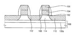
도 1은 본 발명의 실시예 1에 따른 메모리 소자를 나타내는 단면도이다.1 is a cross-sectional view showing a memory device according to a first embodiment of the present invention.
도 1을 참조하면, 매립 산화막(100a, Buried oxide layer)을 포함하는 반도체 기판(100)이 마련된다. 즉, 상기 반도체 기판(100)은 하부 반도체막, 매립 산화막 및 상부 반도체막이 적층된 구조를 가질 수 있다. 상기 반도체 기판(100)은 SOI 기판일 수 있다.Referring to FIG. 1, a
도시되지는 않았지만, 상기 상부 반도체막이 패터닝된 형상을 가짐으로써 소자 분리 영역 및 액티브 영역으로 구분될 수 있다. 상기 소자 분리 영역에는 소자 분리막이 구비된다.Although not shown, the upper semiconductor film may have a patterned shape, so that it can be divided into an element isolation region and an active region. The element isolation region is provided with an element isolation film.
상기 반도체 기판(100) 상에는 게이트 절연막 패턴(102) 및 게이트 전극(104)이 적층된 게이트가 구비된다. 상기 게이트의 양측벽에는 게이트 스페이서(108)가 구비될 수 있다. 상기 게이트 전극(104) 상에는 하드 마스크 패턴(106)이 구비될 수 있다. 상기 게이트 전극(104)은 제1 방향으로 연장되는 라인 형상을 가짐으로써, 워드 라인으로 제공된다.On the
또한, 상기 게이트 양측의 반도체 기판(100) 표면 아래에는 불순물이 도핑된 소오스/드레인(110, 112)이 구비된다.In addition, impurity-doped source /
상기 소오스/드레인(110, 112)의 저면은 상기 매립 산화막(100a) 상부면과 접촉된다. 그러므로, 상기 소오스/드레인(110, 112) 사이의 채널 영역은 상기 매립 산화막(100a), 소오스(110) 및 드레인(112)에 의해 한정된다. 상기 소오스/드레인(110, 112) 사이의 채널 영역은 전기적으로 플로팅되어 있으므로 플로팅 바디(114)가 된다.The bottom surfaces of the source /
상기 소오스/드레인(110, 112)에는 제1 도전형의 불순물이 도핑되어 있으며, 상기 플로팅 바디(114)에는 상기 제1 도전형과 다른 제2 도전형의 불순물이 도핑되어 있다.The source /
설명한 것과 같이, 상기 매립 산화막(100a)을 포함하는 반도체 기판(100) 상에 MOS 트랜지스터가 구비된다.As described above, a MOS transistor is provided on the
상기 MOS 트랜지스터의 플로팅 바디(114)에 홀을 저장하거나 방출함으로써, 상기 MOS 트랜지스터에 데이터를 기록할 수 있다. 또한, 상기 플로팅 바디(114)에 홀이 저장되었는지 여부에 따라 상기 MOS 트랜지스터의 문턱 전압이 변하는 것을 이용하여 상기 MOS 트랜지스터에 저장된 데이터를 읽을 수 있다. 따라서, 상기 MOS 트랜지스터는 휘발성 메모리 소자, 즉 1T 디램 소자로써 기능하게 된다.By storing or discharging holes in the floating
상기 MOS 트랜지스터의 소오스(110)에는 비트 라인 구조물이 전기적으로 연결된다. 상기 비트 라인 구조물은 상기 소오스(110)와 전기적으로 접촉하는 비트 라인 콘택(118) 및 상기 비트 라인 콘택(118)과 전기적으로 연결되는 비트 라인(120)을 포함한다. 상기 비트 라인(120)은 상기 워드 라인의 연장 방향과 수직한 제2 방향으로 연장된다.The bit line structure is electrically connected to the
상기 MOS 트랜지스터의 드레인(112)에는 하부 전극(126), 강유전체 패턴(128) 및 상부 전극(130)을 포함하는 커패시터(132)가 연결된다.A
구체적으로, 상기 드레인(112)과 접촉하는 콘택 플러그(124)를 포함하고, 상기 콘택 플러그(124) 상에 하부 전극(126)이 구비된다. 상기 강유전체 패턴(128)은 PZT[Pb(Zr, Ti)O3], SBT[Sr(Bi, Ta)O3] 또는 BLT[Bi(La, Ti)O3]로 이루어질 수 있다. 상기 커패시터(132)는 상기 비트 라인(120)보다 높게 위치하는 것이 바람직하다. 그러나, 상기 커패시터(132)가 상기 비트 라인(120)보다 낮게 위치할 수도 있다.Specifically, a
상기 상부 전극(130) 상에는 플레이트 라인(134)이 구비된다. 상기 플레이트 라인(134)은 상기 워드 라인과 동일한 방향인 제1 방향으로 연장된다.A
상기 MOS 트랜지스터의 드레인(112)에 연결되는 커패시터(132)의 강유전체 패턴(128)의 극성을 변화시킴으로써 상기 커패시터(132)에 데이터를 저장할 수 있다. 상기 커패시터(132)에 포함된 강유전체 패턴(128)의 극성에 따른 상기 비트 라인(120)의 전압 차이를 이용하여 상기 커패시터(132)에 저장된 데이터를 읽을 수 있다. 따라서, 상기 커패시터(132)는 비휘발성 메모리 소자, 즉 FRAM 소자로써 기능하게 된다.Data can be stored in the
이와같이, 본 실시예에 따른 메모리 소자는 동작 조건에 따라 비휘발성 메모리 소자로 작동되거나 또는 휘발성 메모리 소자로 작동된다. 그러므로, 빠른 재 쓰기가 요구되는 데이터의 경우에는 휘발성 모드로 동작시켜 데이터를 저장하고, 전원 공급 없이도 데이터가 유지하여야 하는 경우에는 비휘발성 모드로 동작시켜 데이터를 저장할 수 있다.Thus, the memory device according to the present embodiment operates as a non-volatile memory device or as a volatile memory device according to operating conditions. Therefore, in the case of data requiring fast rewriting, the data is stored in a volatile mode, and data can be stored in a nonvolatile mode when data is to be maintained without power supply.
이하에서는, 실시예 1의 메모리 소자의 제조 방법을 설명한다.Hereinafter, a method of manufacturing the memory element of the first embodiment will be described.
도 2 내지 도 4는 본 발명의 실시예 1에 따른 메모리 소자의 제조 방법을 설명하기 위한 단면도들이다.FIGS. 2 to 4 are cross-sectional views illustrating a method of manufacturing a memory device according to a first embodiment of the present invention.
도 2를 참조하면, 매립 산화막(100a, Buried oxide layer)을 포함하는 반도체 기판(100)이 마련된다. 즉, 상기 반도체 기판(100)은 하부 반도체막, 매립 산화막 및 상부 반도체막이 적층된 구조를 가질 수 있다. 상기 반도체 기판은 SOI(silicon on insulator) 기판일 수 있다. 도시하지는 않았지만, 소자 분리 공정을 수행하여 상기 반도체 기판(100)을 액티브 영역 및 소자 분리 영역으로 구분할 수 있다.Referring to FIG. 2, a
상기 반도체 기판(100) 표면에 불순물을 도핑시켜 채널 도핑 영역을 형성한다.Impurities are doped on the surface of the
상기 반도체 기판(100) 상에, 게이트 절연막, 게이트 전극막 및 하드 마스크 패턴(106)을 형성하고, 상기 하드 마스크 패턴(106)을 식각 마스크로 사용하여 상기 게이트 전극막 및 게이트 절연막을 식각함으로써 게이트 전극(104) 및 게이트 절연막 패턴(102)을 형성한다.A gate insulating film, a gate electrode film and a
상기 게이트 전극(104)은 제1 방향으로 연장되는 라인 형상을 갖도록 형성된다. 상기 게이트 전극(104)은 워드 라인으로 사용된다.The
다음에, 상기 게이트 전극(104) 및 반도체 기판(100) 표면에 스페이서용 절연막을 형성하고, 상기 스페이서용 절연막을 이방성 식각하여 스페이서(108)를 형성한다.Next, an insulating film for a spacer is formed on the surface of the
상기 게이트 전극(104) 양측의 반도체 기판(100) 표면 아래로 상기 채널 도핑 영역의 불순물과 다른 도전형을 갖는 불순물을 주입시켜 소오스 및 드레인(110, 112)을 형성한다. 상기 소오스(110) 및 드레인(112)의 저면은 상기 매립 산화막(100a) 상부면과 접하도록 한다.The source and drain
상기 소오스/드레인을 형성하면, 상기 소오스/드레인 및 매립 산화막에 의해 한정되는 영역이 플로팅 바디가 된다.When the source / drain is formed, a region defined by the source / drain and the buried oxide film becomes a floating body.
상기 설명한 공정들을 수행함으로써, 휘발성 메모리 소자로 사용되는 MOS 트랜지스터를 완성한다. 본 실시예에서는, 도시된 것과 같이, 상기 소오스(110)를 공통으로 사용하는 2개의 MOS 트랜지스터를 형성하는 것으로 설명한다.By performing the above-described processes, a MOS transistor used as a volatile memory device is completed. In the present embodiment, it is assumed that two MOS transistors commonly using the
도 3을 참조하면, 상기 MOS 트랜지스터를 덮는 제1 층간 절연막(116)을 형성한다.Referring to FIG. 3, a first
상기 제1 층간 절연막(116)의 일 부분을 식각하여 상기 MOS 트랜지스터의 소오스를 노출시키는 제1 콘택홀을 형성한다. 상기 제1 콘택홀 내부에 도전물질을 채워넣음으로써 비트 라인 콘택(118)을 형성한다. 상기 제1 층간 절연막(116) 상에는 상기 비트 라인 콘택(118)과 접하면서 상기 제1 방향과 수직한 제2 방향으로 연장되는 비트 라인(120)을 형성한다.A portion of the first
상기 비트 라인 콘택(118) 및 비트 라인(120)은 각각의 형성 공정들을 순차적으로 수행하여 형성될 수 있다. 이와는 달리, 상기 비트 라인 콘택(118) 및 비트 라인(120)은 도전 물질 증착 및 1회의 패터닝 공정을 통해 동시에 형성될 수도 있다.The
도시하지는 않았지만, 다른 실시예로, 상기 비트 라인 콘택(116)을 형성하는 공정에서, 상기 커패시터와 연결되는 패드 콘택을 함께 형성할 수도 있다.Although not shown, in another embodiment, in the process of forming the
도 4를 참조하면, 상기 제1 층간 절연막(116) 및 비트 라인(120) 상에 제2 층간 절연막(122)을 형성한다.Referring to FIG. 4, a second
상기 제2 층간 절연막(122) 및 제1 층간 절연막(116)의 일부 영역을 순차적으로 식각함으로써 상기 MOS 트랜지스터의 드레인(112)을 노출시키는 제2 콘택홀을 형성한다.A second contact hole exposing the
이와는 다른 실시예로, 상기 비트 라인 콘택(118)을 형성하는 공정에서 패드 콘택을 형성한 경우에는 상기 패드 콘택의 상부면을 노출시키는 제2 콘택홀을 형성한다.In another embodiment, when the pad contact is formed in the process of forming the
상기 제2 콘택홀 내부에 도전 물질을 채워넣음으로써 콘택 플러그(124)를 형성한다.A
다음에, 상기 제2 층간 절연막(122) 및 콘택 플러그(124)를 덮는 하부 전극막을 형성한다. 상기 하부 전극막은 이리듐, 이리듐 산화물, 백금 , 스트론튬 루테 늄 산화물(SRO) 등으로 이루어질 수 있다. 이들은 단독으로 사용되거나 또는 2 이상을 적층시켜 사용할 수 있다. 예를들어, 상기 이리듐, 이리듐 산화물 및 백금을 순차적으로 적층시켜 상기 하부 전극막을 형성할 수 있다.Next, a lower electrode film covering the second
상기 하부 전극막 상에 강유전체막을 형성한다. 상기 강유전체막은 PZT[Pb(Zr, Ti)O3], SBT[Sr(Bi, Ta)O3] 또는 BLT[Bi(La, Ti)O3]로 이루어질 수 있다.A ferroelectric film is formed on the lower electrode film. The ferroelectric film may be made of PZT [Pb (Zr, Ti) O3 ], SBT [Sr (Bi, Ta) O3 ], or BLT [Bi (La, Ti) O3 ].
상기 강유전체막 상에 상부 전극막을 형성한다. 상기 상부 전극막은 이리듐 산화물, 이리듐, 트론튬 루테늄 산화물(SRO) 등으로 이루어질 수 있다. 이들은 단독으로 사용되거나 또는 이들을 적층시켜 사용할 수 있다. 예를들어, 상기 이리듐 산화물 및 이리듐을 순차적으로 적층시켜 상기 상부 전극막을 형성할 수 있다.And an upper electrode film is formed on the ferroelectric film. The upper electrode layer may be formed of iridium oxide, iridium, tronium ruthenium oxide (SRO), or the like. These may be used alone or may be used by laminating them. For example, the upper electrode film may be formed by sequentially laminating the iridium oxide and iridium.
상기 하부 전극막, 강유전체막 및 상부 전극막을 패터닝함으로써 하부 전극(126), 강유전체 패턴(128) 및 상부 전극(130)이 적층된 커패시터(132)를 형성한다.The lower electrode film, the ferroelectric film, and the upper electrode film are patterned to form a
이 후, 상기 커패시터(132)의 상부 전극(130)과 전기적으로 접촉하는 플레이트 라인(134)을 형성한다. 상기 플레이트 라인(134)은 상기 워드 라인과 동일한 방향으로 연장되는 라인 형상을 갖는다. 상기 플레이트 라인(134)은 금속 물질로 형성될 수 있다. 상기 플레이트 라인(134)으로 사용될 수 있는 금속 물질의 예로는 알루미늄을 들 수 있다.Thereafter, a
이하에서는, 실시예 1의 메모리 소자의 동작 방법을 설명한다.Hereinafter, an operation method of the memory element of the first embodiment will be described.
플로팅 바디에 데이터를 저장하는 방법How to store data in a floating body
상기 메모리 소자를 휘발성 모드로 동작할 때, 메모리 소자의 플로팅 바디에 데이터를 저장하는 방법을 설명한다.A method of storing data in a floating body of a memory element when the memory element operates in a volatile mode will be described.
상기 휘발성 모드로 동작시킬 때에는 상기 커패시터는 데이터를 저장하는 기능을 하지 않는다. 즉, 상기 휘발성 모드로 동작되는 경우에는 1T DRAM으로만 사용된다. 따라서, 상기 커패시터에 의하여 상기 플로팅 바디에 저장되는 데이터가 변경되지 않도록 한다.When operating in the volatile mode, the capacitor does not function to store data. That is, when operated in the volatile mode, it is used only as a 1T DRAM. Thus, the data stored in the floating body is not changed by the capacitor.
<휘발성 모드의 데이터 1 기록>≪ Recording of volatile mode data 1 >
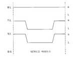
도 5는 상기 휘발성 모드로 데이터 1을 쓸 때의 전압 신호를 나타낸다.5 shows voltage signals when data 1 is written in the volatile mode.
도 1 및 도 5를 참조하여 상기 플로팅 바디(114)에 홀을 저장시켜 데이터 1을 쓰는 경우를 설명하면, 우선 채널 영역 아래의 기판에 백 게이트 전압을 인가한다. 상기 백 게이트 전압은 네거티브 바이어스이며, 예를들어 -20 내지 -40V 로 인가될 수 있다. 상기 플레이트 라인(134)은 접지 상태가 되도록 함으로써 커플링에 의해 상기 소오스(110)가 접지 상태가 되도록 한다.Referring to FIGS. 1 and 5, a case where data is written in the floating
상기 워드 라인(104)에 하이 신호를 인가하여 MOS 트랜지스터를 턴 온 시킨다. 또한, 상기 비트 라인(120)은 대기 상태에서 하이 신호로 변화시킨다.A high signal is applied to the
이 경우, 상기 드레인(112) 근처의 플로팅 바디(114)에는 전자-홀 쌍들이 발생된다. 그리고, 상기 전자들은 상기 소오스(110) 및 드레인(112)을 통해 소거되며, 상기 홀들은 상기 플로팅 바디(114)에 축적된다. 상기 플로팅 바디(114)에 축 적된 전하에 의해 상기 플로팅 바디(114)의 전위가 상승되고, 이로인해 상기 MOS 트랜지스터의 문턱 전압이 낮아지게 된다. 상기와 같은 홀 주입을 충격 이온화 방식이라 한다.In this case, electron-hole pairs are generated in the floating
이와같이, 상기 백 게이트 전압에 의해 상기 홀이 축적되기 때문에, 상기 커패시터에는 데이터가 기록되지 않는다.Thus, since the holes are accumulated by the back gate voltage, no data is written to the capacitor.
도시하지는 않았지만, 상기 설명한 것과 다른 방법으로 데이터 1을 쓸 수 있다.Although not shown, data 1 can be written in a manner different from that described above.
구체적으로, 상기 도 5를 참조로 설명한 것과 동일하게, 채널 영역 아래의 기판에 네거티브 바이어스로써 백 게이트 전압을 인가한다. 상기 플레이트 라인은 접지 상태가 되도록 함으로써 커플링에 의해 상기 소오스가 접지 상태가 되도록 한다. 또한, 상기 비트 라인(120)에는 하이 신호를 인가한다.Specifically, as described with reference to FIG. 5, a back gate voltage is applied to the substrate under the channel region with a negative bias. The plate line is grounded so that the source is grounded by coupling. In addition, a high signal is applied to the
상기 도 5를 참조로 설명한 것과 다르게, 상기 워드 라인(104)에 음 전압의 신호를 인가한다.A negative voltage signal is applied to the
이 경우, 상기 소오스(110) 및 드레인(112) 근처의 플로팅 바디(114)에는 전자 홀 쌍들이 발생된다. 상기 전자들은 상기 소오스(110) 및 상기 드레인(112)을 통하여 소거된다. 반면, 상기 홀들은 상기 플로팅 바디(114) 내에 축적된다. 상기 축적된 홀들은 상기 플로팅 바디(114)의 전위를 상승시킨다. 상기 플로팅 바디(114)의 전위 상승에 의하여 상기 MOS 트랜지스터의 문턱 전압은 낮아지게 된다. 상기와 같은 홀 주입을 GIDL을 이용한 주입 방식이라 한다.In this case, pairs of electron holes are generated in the floating
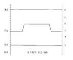
<휘발성 모드의 데이터 0 기록>≪ Recording data 0 in volatile mode >
도 6은 상기 휘발성 모드로 데이터 0을 쓸 때의 전압 신호를 나타낸다.6 shows a voltage signal when data 0 is written in the volatile mode.
도 1 도 6을 참조하여 상기 플로팅 바디(114)에 홀을 방출시켜 데이터 0을 쓰는 경우를 설명하면, 우선 채널 영역 아래의 기판에 백 게이트 전압을 인가한다. 상기 백 게이트 전압은 네거티브 바이어스이며, 예를들어 -20 내지 -40V 로 인가될 수 있다. 상기 플레이트 라인은 접지 상태가 되도록 함으로써 커플링에 의해 상기 소오스가 접지 상태가 되도록 한다.Referring to FIG. 1, a case where data 0 is written to the floating
상기 워드 라인(104)에 하이 신호를 인가하여 MOS 트랜지스터를 턴 온 시킨다. 또한, 상기 비트 라인(120)은 대기 상태에서 로우 신호가 되도록 변화시킨다. 즉, 상기 비트 라인(120)은 접지되도록 하거나 또는 음 전압을 인가시킬 수 있다.A high signal is applied to the
이 경우, 상기 플로팅 바디(114)에 축적된 홀들은 드레인(112)을 통해 소거된다.In this case, the holes accumulated in the floating
커패시터에 데이터를 저장하는 방법How to Store Data on a Capacitor
비휘발성 모드로 동작할 때, 메모리 소자의 커패시터에 데이터를 저장하는 방법을 설명한다. 상기 비휘발성 모드로 동작시킬 때에는 상기 플로팅 바디에는 데이터를 저장하는 역할을 하지 않는다. 즉, 상기 메모리 소자는 FRAM 소자로만 사용된다.A method of storing data in a capacitor of a memory element when operating in a non-volatile mode will be described. And does not store data in the floating body when operating in the nonvolatile mode. That is, the memory device is used only as an FRAM device.
<비휘발성 모드의 데이터 1 기록>≪ Recording data 1 in nonvolatile mode >
도 7은 상기 비휘발성 모드로 데이터 1을 쓸 때의 전압 신호를 나타낸다.7 shows a voltage signal when data 1 is written in the nonvolatile mode.
도 1 및 도 7을 참조하여 상기 커패시터(132)에 데이터 1을 쓰는 경우를 설 명하면, 우선 채널 영역 아래의 기판에 양 전압을 인가하거나 또는 접지 상태가 되도록 한다. 상기 커패시터에는 플레이트 라인과 비트 라인의 전압 차이를 통해 분극 상태가 결정되어 데이터가 기록되므로, 상기 기판이 양 전압 또는 접지 상태가 되더라도 데이터 기록에는 영향이 없다.Referring to FIGS. 1 and 7, when data 1 is written to the
이와같이, 상기 비휘발성 모드로 동작되는 경우에는 네거티브 바이어스인 백 게이트 전압이 인가되지 않는다. 때문에, 상기 플로팅 바디에는 홀이 축적되지 않으므로, 상기 메모리 소자에 포함되어 있는 트랜지스터는 단지 스위칭 소자로만 사용된다. 이와같이, 상기 메모리 소자는 백 게이트 전압의 레벨에 따라 비휘발성 모드 또는 휘발성 모드로 각각 구분될 수 있다.In this way, when the nonvolatile mode is operated, a back gate voltage which is a negative bias is not applied. Therefore, since no holes are accumulated in the floating body, the transistor included in the memory element is used only as a switching element. In this way, the memory device can be divided into a non-volatile mode or a volatile mode, respectively, depending on the level of the back gate voltage.
상기 워드 라인(104)에 하이 신호를 인가하여 상기 MOS 트랜지스터를 턴 온 시킨다. 상기 비트 라인(120)은 대기 상태에서 하이 상태로 변화시킨다. 또한, 상기 플레이트 라인(134)에는 계속하여 로우 신호를 인가한다. 즉, 상기 플레이트 라인(134)은 접지시킬 수 있다. 이 경우, 상기 커패시터(132)는 데이터 1의 분극 상태(polarization state)를 갖게 된다.A high signal is applied to the
<비휘발성 모드의 데이터 0 기록>≪ Data 0 recording in nonvolatile mode >
도 8은 상기 비휘발성 모드로 데이터 0을 쓸 때의 전압 신호를 나타낸다.8 shows a voltage signal when data 0 is written in the nonvolatile mode.
도 1 및 도 8을 참조하여 상기 커패시터(132)에 데이터 0을 쓰는 경우를 설명하면, 우선 채널 영역 아래의 기판에 양 전압을 인가하거나 또는 접지 상태가 되도록 한다.Referring to FIGS. 1 and 8, a case where data 0 is written to the
상기 워드 라인(104)에 하이 신호를 인가하여 상기 MOS 트랜지스터를 턴 온 시킨다. 상기 비트 라인(120)에도 계속하여 로우 신호를 인가한다. 즉, 상기 비트 라인(120)은 접지시킬 수 있다. 또한, 상기 플레이트 라인(134)은 대기 상태에서 하이 상태로 변화시킨다.A high signal is applied to the
이 경우, 상기 커패시터(132)는 데이터 1과 반대인 데이터 0의 분극 상태(polarization state)를 갖게 된다.In this case, the
이와같이, 본 실시예에 따른 메모리 소자에 데이터를 기록할 수 있다.Thus, data can be recorded in the memory device according to the present embodiment.
상기에서 설명한 것과 같이, 상기 설명한 메모리 소자는 선택된 동작 모드에 따라 휘발성 메모리 소자 및 비휘발성 메모리 소자 중 어느 하나의 소자로만 동작된다. 때문에, 상기 메모리 소자에 기록되어 있는 데이터를 읽는 방법은 상기 메모리 소자의 동작 모드별로 달라지게 된다.As described above, the above-described memory element operates only as an element of either the volatile memory element or the non-volatile memory element in accordance with the selected operation mode. Therefore, the method of reading data recorded in the memory device varies depending on the operation mode of the memory device.
본 실시예의 메모리 소자가 휘발성 모드로 동작하는 경우에는, 1T DRAM의 읽기 동작이 수행된다. 반면에, 본 실시예의 메모리 소자가 비휘발성 모드로 동작하는 경우에는, FRAM의 읽기 동작이 수행된다.When the memory device of this embodiment operates in the volatile mode, the read operation of the 1T DRAM is performed. On the other hand, when the memory device of this embodiment operates in the nonvolatile mode, the read operation of the FRAM is performed.
실시예 2Example 2
도 9는 본 발명의 실시예 2에 따른 메모리 소자를 나타내는 단면도이다.9 is a cross-sectional view showing a memory device according to a second embodiment of the present invention.
도 9를 참조하면, 매립 산화막(100a, Buried oxide layer)을 포함하는 반도체 기판(100)이 마련된다.Referring to FIG. 9, a
상기 반도체 기판(100) 상에는 게이트 절연막 패턴(102) 및 게이트 전극(104)이 적층된 게이트가 구비된다. 상기 게이트의 양측벽에는 게이트 스페이 서(108)가 구비될 수 있다. 상기 게이트 전극(104)은 제1 방향으로 연장되는 라인 형상을 가짐으로써, 워드 라인으로 제공된다.On the
또한, 상기 게이트 양측의 반도체 기판(100) 표면 아래에는 불순물이 도핑된 소오스/드레인(110, 112)이 구비된다. 상기 소오스/드레인(110, 112)의 저면은 상기 매립 산화막(100a) 상부면과 접촉된다. 그러므로, 상기 소오스/드레인(110, 112) 사이의 채널 영역은 상기 매립 산화막(100a), 소오스 및 드레인(110, 112)에 의해 한정된다. 상기 소오스/드레인(110, 112) 사이의 채널 영역은 전기적으로 플로팅되어 있으므로 플로팅 바디(114)가 된다.In addition, impurity-doped source /
즉, 도시된 것과 같이, 상기 매립 산화막(100a)을 포함하는 기판(100) 상에 실시예 1과 동일한 구조의 MOS 트랜지스터가 구비된다.That is, as shown in the figure, a MOS transistor having the same structure as that of the first embodiment is provided on the
상기 MOS 트랜지스터의 플로팅 바디(114)에 홀을 저장하거나 방출함으로써, 상기 MOS 트랜지스터에 데이터를 기록할 수 있다. 또한, 상기 플로팅 바디(114)에 홀이 저장되었는지 여부에 따라 상기 MOS 트랜지스터의 문턱 전압이 변하는 것을 이용하여 상기 MOS 트랜지스터에 저장된 데이터를 읽을 수 있다. 따라서, 상기 MOS 트랜지스터는 휘발성 메모리 소자 즉, 1TDRAM으로써 기능하게 된다.By storing or discharging holes in the floating
상기 MOS 트랜지스터의 소오스(110)에는 비트 라인 콘택(118)이 연결된다. 또한, 상기 비트 라인 콘택(118) 상부면에는 비트 라인(120)이 구비된다. 상기 비트 라인(120)은 상기 워드 라인의 연장 방향과 수직한 제2 방향으로 연장된다.A
상기 MOS 트랜지스터의 드레인(112)에는 하부 전극, 상전이 패턴(142) 및 상부 전극(146)을 포함하는 전하 저장용 구조물이 연결된다. 상기 하부 전극은 상기 드레인(112)과 접촉하는 콘택 플러그(140)의 형상을 가질 수 있다. 상기 상전이 패턴(142)은 칼코겐 물질로 이루어질 수 있다. 상기 상부 전극(146)은 라인 형상을 갖고 있어 이웃하는 상전이 패턴(142)과 동시에 연결될 수 있다.A charge storage structure including a lower electrode, a
상기 전하 저장용 구조물은 상기 비트 라인(120)보다 높게 위치하는 것이 바람직하다. 그러나, 상기 전하 저장용 구조물이 상기 비트 라인(120)보다 낮게 위치할 수도 있다.The charge storage structure is preferably located higher than the
상기 전하 저장용 구조물에 포함된 상전이 패턴(142)의 상을 변화시킴으로써 데이터를 저장할 수 있다. 즉, 상기 상전이 패턴(142)의 상이 결정상인 경우에는 저저항을 갖게되어 상기 상전이 패턴(142) 양단에 전류가 흐르는 데이터 0 상태가 된다. 반면에, 상기 상전이 패턴(142)의 상이 비정질상인 경우에는 고저항을 갖게되어 상기 상전이 패턴(142) 양단에 전류가 흐르지 않는 1 상태가 된다. 따라서, 상기 전하 저장용 구조물은 비휘발성 메모리 소자, 즉 PRAM 소자로써 기능하게 된다.Data can be stored by changing the phase of the
즉, 본 실시예에 따른 메모리 소자는 동작 조건에 따라 비휘발성 메모리 소자로 작동되거나 또는 휘발성 메모리 소자로 작동된다.That is, the memory device according to the present embodiment operates as a non-volatile memory device or as a volatile memory device depending on operating conditions.
그러므로, 빠른 재쓰기가 요구되는 메모리 소자가 요구되는 경우에는 휘발성 메모리 소자로 동작시킬 수 있다. 또한, 전원 공급 없이도 데이터가 유지되어야 하는 메모리 소자가 요구되는 경우에는 비휘발성 메모리 소자 로 동작시킬 수 있다.Therefore, when a memory element requiring fast rewriting is required, it can be operated as a volatile memory element. In addition, when a memory element requiring data to be held without power supply is required, it can be operated as a nonvolatile memory element.
이하에서는, 실시예 2의 메모리 소자의 제조 방법을 설명한다.Hereinafter, a method of manufacturing the memory element of the second embodiment will be described.
도 10 및 도 11은 본 발명의 실시예 2에 따른 메모리 소자의 제조 방법을 설명하기 위한 단면도들이다.10 and 11 are cross-sectional views illustrating a method of manufacturing a memory device according to a second embodiment of the present invention.
도 10을 참조하면, 매립 산화막(100a, Buried oxide layer)을 포함하는 반도체 기판(100)에 MOS 트랜지스터를 형성한다. 상기 MOS 트랜지스터를 형성하는 공정은 도 2를 참조로 설명한 것과 동일하다.Referring to FIG. 10, a MOS transistor is formed on a
상기 MOS 트랜지스터를 덮는 제1 층간 절연막(116)을 형성한다. 상기 제1 층간 절연막(116)을 관통하여 상기 MOS 트랜지스터의 소오스(110)와 접촉하는 비트 라인 콘택(118) 및 상기 제1 층간 절연막(116) 상에 비트 라인 콘택(118)과 접하는 비트 라인(120)을 각각 형성한다. 상기 제1 층간 절연막(116), 비트 라인 콘택(118) 및 비트 라인(120)을 형성하는 공정은 도 3을 참조로 설명한 것과 동일하다.A first
상기 제1 층간 절연막(116) 및 비트 라인(120) 상에 제2 층간 절연막(122)을 형성한다. 상기 제2 층간 절연막(122) 및 제1 층간 절연막(116)의 일부 영역을 순차적으로 식각함으로써 상기 MOS 트랜지스터의 드레인(112)을 노출시키는 제2 콘택홀을 형성한다. 상기 제2 콘택홀 내부에 도전 물질을 채워넣음으로써 콘택 플러그(140)를 형성한다. 상기 콘택 플러그(140)는 전하 저장 구조물의 하부 전극으로 제공된다.A second
도 11을 참조하면, 상기 콘택 플러그(140) 및 제2 층간 절연막(122) 상에 상전이막을 형성한다. 상기 상전이막은 칼코겐 합금 물질을 포함한다. 즉, 상기 상전 이막은 게르마늄, 안티몬, 텔루르를 포함한다.Referring to FIG. 11, a phase change film is formed on the
이 후, 상기 상전이막을 패터닝함으로써 상전이 패턴(142)을 형성한다. 상기 상전이 패턴(142)은 상기 콘택 플러그(140) 상부면을 완전히 덮도록 형성한다. 그러므로, 상기 상전이 패턴(142)은 상기 콘택 플러그(140)의 상부면 보다 더 넓은 저면을 갖게된다.Thereafter, the
다음에, 상기 상전이 패턴(142)들 사이에 절연막 패턴(144)을 형성한다. 상기 상전이 패턴(142)들 상에는 상부 전극(146)을 형성한다. 상기 상부 전극(146)은 이웃하는 상전이 패턴들과 함께 연결되도록 형성된다.Next, an insulating
이하에서는, 실시예 2의 메모리 소자의 동작 방법을 설명한다.Hereinafter, an operation method of the memory element of the second embodiment will be described.
플로팅 바디에 데이터를 저장하는 방법How to store data in a floating body
도 9를 참조로 하여, 휘발성 모드로 동작할 때, 메모리 소자의 플로팅 바디에 데이터를 저장하는 방법을 설명한다.Referring to FIG. 9, a method of storing data in a floating body of a memory element when operating in a volatile mode will be described.
상기 휘발성 모드로 동작시킬 때에는 상기 전하 저장용 구조물에 데이터가 저장되지 않는다. 그러므로, 1T DRAM과 동일하게 동작된다.When operating in the volatile mode, no data is stored in the charge storage structure. Therefore, it operates in the same manner as a 1T DRAM.
실시예 2의 메모리 소자에서 플로팅 바디에 1을 쓰는 방법에 대해 먼저 설명한다. 상기 플로팅 바디에 1을 쓰는 방법은 충격 이온화 방법 및 GIDL을 이용한 방법이 있다.The method of writing 1 to the floating body in the memory element of the second embodiment will be described first. A method of writing 1 to the floating body is a shock ionization method and a method using GIDL.
상기 충격 이온화 방법에 의하면, 워드 라인, 비트 라인 및 기판에 인가되는 바이어스는 도 5를 참조로 설명한 휘발성 모드의 데이터 1 기록 방법과 동일하게 되도록 한다. 구체적으로, 상기 채널 영역이 되는 기판에는 음 전압을 인가한다. 상기 워드 라인(104)에 하이 신호를 인가하여 MOS 트랜지스터를 턴 온 시킨다. 또한, 상기 비트 라인(120)은 하이 신호로 변화시킨다.According to the impact ionization method, the bias applied to the word line, the bit line, and the substrate is made to be the same as the data 1 recording method of the volatile mode described with reference to FIG. Specifically, a negative voltage is applied to the substrate serving as the channel region. A high signal is applied to the
또한, 상부 전극이 접지 상태가 되도록 한다. 상기 상부 전극을 접지시키면, 상기 상전이 패턴 및 하부 전극이 저항으로 작용하여 상기 소오스가 접지된다.Further, the upper electrode is grounded. When the upper electrode is grounded, the phase change pattern and the lower electrode act as resistors, and the source is grounded.
상기 GIDL을 이용한 방법에 의하면, 상기 채널 영역이 되는 기판에는 음 전압을 인가한다. 상기 워드 라인(104)에 음 전압의 신호를 인가한다. 상기 비트 라인(120)은 하이 신호로 변화시킨다. 또한, 상부 전극이 접지 상태가 되도록 함으로써 상기 소오스가 접지 상태가 되도록 한다.According to the method using the GIDL, a negative voltage is applied to the substrate serving as the channel region. And a negative voltage signal is applied to the
상기와 같이 전기적 신호를 인가하면, 상기 플로팅 바디(114)에 홀이 주입되어 상기 MOS 트랜지스터의 문턱 전압은 낮아지게 된다.When an electrical signal is applied as described above, holes are injected into the floating
전하 저장 구조물에 데이터를 저장하는 방법Method for storing data in a charge storage structure
비휘발성 모드로 동작할 때, 메모리 소자의 전하 저장 구조물에 데이터를 저장하는 방법을 설명한다. 상기 비휘발성 모드로 동작시키는 경우, 상기 플로팅 바디에는 데이터가 저장되지 않는다. 즉, 상기 메모리 소자에 포함된 트랜지스터는 스위칭 소자로만 사용된다. 따라서, 상기 트랜지스터의 플로팅 바디에 홀이 축적되지 않도록 상기 채널 영역에 해당하는 기판은 접지되거나 양 전압이 인가되어야 한다.A method of storing data in a charge storage structure of a memory device when operating in a non-volatile mode is described. When operating in the non-volatile mode, no data is stored in the floating body. That is, the transistor included in the memory element is used only as a switching element. Therefore, the substrate corresponding to the channel region must be grounded or a positive voltage must be applied so that holes are not accumulated in the floating body of the transistor.
상기 전하 저장 구조물에 데이터 1을 쓰는 경우, 상기 상전이 패턴(142)에 대하여 단시간에 높은 전류 펄스를 가하여야 한다. 즉, 상전이 패턴(142)이 용융 온도보다 높은 온도로 가열된 후 (전류 펄스에 의한 저항 가열) 아주 짧은 시간동안 냉각되면 상전이 패턴(142)은 비정질 상태가 된다.When data 1 is written to the charge storage structure, a high current pulse should be applied to the
이를 위하여, 상기 워드 라인(104)을 턴 온시킨 후 상기 비트 라인(120)에 높은 전압이 인가되어야 한다. 즉, 상기 비트 라인(120)으로 인가되는 전압을 쓰기 구간동안 펌프시켜 상기 상전이 패턴(142)에 높은 전류가 가해지도록 하여야 한다. 따라서, 상기 쓰기 구간동안에는 상기 비트 라인(120)에서 인가되는 전압을 펌프시킬 수 있는 구동회로를 작동시켜야 한다.For this, a high voltage must be applied to the
반면에, 상기 전하 저장 구조물에 데이터 0을 쓰는 경우, 상대적으로 상기 상전이 패턴(142)에 긴 시간동안 낮은 전류 펄스를 가해야 한다. 그러므로, 상기 상전이 패턴(142)의 용융 온도보다 낮고 결정화 온도보다는 높은 온도로 가열된 후 긴 시간동안 유지된 후 냉각되면 결정 상태가 된다.On the other hand, when data 0 is written to the charge storage structure, a relatively low current pulse should be applied to the
이를 위하여, 상기 워드 라인(104)을 턴 온시킨 후 상기 비트 라인(120)에 상기 데이터 1을 쓰는 동작보다 낮은 전압이 인가되어야 한다. 즉, 상기 쓰기 구간 동안 비트 라인(120)의 전압을 펌프시키는 동작이 요구되지 않는다.For this, a lower voltage than the operation of writing the data 1 to the
설명한 것과 같이, 본 실시예에 따른 메모리 소자는 전압 펌프 동작의 유무에 따라 비휘발성 메모리 또는 휘발성 메모리로 동작될 수 있다.As described, the memory device according to the present embodiment can be operated as a nonvolatile memory or a volatile memory depending on the presence or absence of a voltage pump operation.
이와같이, 본 실시예에 따른 메모리 소자는 하나의 동작 모드가 선택됨으로써 휘발성 메모리 소자 및 비휘발성 메모리 소자 중 어느 하나의 소자로만 동작된다. 때문에, 상기 메모리 소자에 기록되어 있는 데이터를 읽는 방법은 상기 메모리 소자의 동작 모드별로 달라지게 된다.Thus, the memory device according to the present embodiment operates only as one of the volatile memory device and the non-volatile memory device by selecting one operation mode. Therefore, the method of reading data recorded in the memory device varies depending on the operation mode of the memory device.
본 실시예의 메모리 소자가 휘발성 모드로 동작하는 경우에는, 1T DRAM의 읽기 동작이 수행된다. 반면에, 본 실시예의 메모리 소자가 비휘발성 모드로 동작하는 경우에는, PRAM의 읽기 동작이 수행된다.When the memory device of this embodiment operates in the volatile mode, the read operation of the 1T DRAM is performed. On the other hand, when the memory element of this embodiment operates in the nonvolatile mode, the read operation of the PRAM is performed.
상기 설명한 것과 같이, 본 발명은 비휘발성 메모리 및 휘발성 메모리를 모두 요구하는 다양한 전자제품 및 통신 제품에 적용할 수 있다. 또한, 하나의 메모리 소자에서 상기 비휘발성 메모리 및 휘발성 메모리 특성을 가지므로, 고집적화된 소자를 요구하는 전자 제품에 적용될 수 있다.As described above, the present invention can be applied to various electronic products and communication products requiring both non-volatile memory and volatile memory. In addition, since the nonvolatile memory and the volatile memory characteristics are provided in one memory element, the present invention can be applied to an electronic product requiring a highly integrated device.
도 1은 본 발명의 실시예 1에 따른 메모리 소자를 나타내는 단면도이다.1 is a cross-sectional view showing a memory device according to a first embodiment of the present invention.
도 2 내지 도 4는 본 발명의 실시예 1에 따른 메모리 소자의 제조 방법을 설명하기 위한 단면도들이다.FIGS. 2 to 4 are cross-sectional views illustrating a method of manufacturing a memory device according to a first embodiment of the present invention.
도 5는 휘발성 모드로 데이터 1을 쓸 때의 전압 신호를 나타낸다.5 shows the voltage signal when data 1 is written in the volatile mode.
도 6은 휘발성 모드로 데이터 0을 쓸 때의 전압 신호를 나타낸다.6 shows a voltage signal when data 0 is written in the volatile mode.
도 7은 비휘발성 모드로 데이터 1을 쓸 때의 전압 신호를 나타낸다.7 shows a voltage signal when data 1 is written in a nonvolatile mode.
도 8은 비휘발성 모드로 데이터 0을 쓸 때의 전압 신호를 나타낸다.8 shows a voltage signal when data 0 is written in the nonvolatile mode.
도 9는 본 발명의 실시예 2에 따른 메모리 소자를 나타내는 단면도이다.9 is a cross-sectional view showing a memory device according to a second embodiment of the present invention.
도 10 및 도 11은 본 발명의 실시예 2에 따른 메모리 소자의 제조 방법을 설명하기 위한 단면도들이다.10 and 11 are cross-sectional views illustrating a method of manufacturing a memory device according to a second embodiment of the present invention.
Claims (20)
Translated fromKoreanPriority Applications (3)
| Application Number | Priority Date | Filing Date | Title |
|---|---|---|---|
| KR1020080071995AKR101415509B1 (en) | 2008-07-24 | 2008-07-24 | MEMORY DEVICE, METHOD OF MANUFACTURING THE SAME |
| US12/458,800US8253201B2 (en) | 2008-07-24 | 2009-07-23 | Memory device |
| TW098125065ATWI532147B (en) | 2008-07-24 | 2009-07-24 | Memory device and method of operating same |
Applications Claiming Priority (1)
| Application Number | Priority Date | Filing Date | Title |
|---|---|---|---|
| KR1020080071995AKR101415509B1 (en) | 2008-07-24 | 2008-07-24 | MEMORY DEVICE, METHOD OF MANUFACTURING THE SAME |
Publications (2)
| Publication Number | Publication Date |
|---|---|
| KR20100010977A KR20100010977A (en) | 2010-02-03 |
| KR101415509B1true KR101415509B1 (en) | 2014-07-04 |
Family
ID=41567853
Family Applications (1)
| Application Number | Title | Priority Date | Filing Date |
|---|---|---|---|
| KR1020080071995AActiveKR101415509B1 (en) | 2008-07-24 | 2008-07-24 | MEMORY DEVICE, METHOD OF MANUFACTURING THE SAME |
Country Status (3)
| Country | Link |
|---|---|
| US (1) | US8253201B2 (en) |
| KR (1) | KR101415509B1 (en) |
| TW (1) | TWI532147B (en) |
Families Citing this family (5)
| Publication number | Priority date | Publication date | Assignee | Title |
|---|---|---|---|---|
| FR3001333B1 (en)* | 2013-01-22 | 2016-05-06 | Soitec Silicon On Insulator | REAR GRID IN SELECTION TRANSISTOR FOR EMBEDDED DRAM |
| TWI503964B (en)* | 2013-03-13 | 2015-10-11 | Winbond Electronics Corp | Resistive random access memory device |
| FR3038132B1 (en) | 2015-06-23 | 2017-08-11 | St Microelectronics Crolles 2 Sas | RESISTIVE MEMORY CELL HAVING A COMPACT STRUCTURE |
| FR3038133B1 (en)* | 2015-06-23 | 2017-08-25 | St Microelectronics Crolles 2 Sas | PHASE CHANGE MEMORY CELL HAVING A COMPACT STRUCTURE |
| US11411123B2 (en)* | 2019-08-30 | 2022-08-09 | Taiwan Semiconductor Manufacturing Company Limited | Semiconductor device and method of formation |
Citations (2)
| Publication number | Priority date | Publication date | Assignee | Title |
|---|---|---|---|---|
| JPH1065115A (en)* | 1996-08-13 | 1998-03-06 | Hitachi Ltd | Semiconductor integrated circuit device |
| JP2008153633A (en)* | 2006-11-16 | 2008-07-03 | Samsung Electronics Co Ltd | Resistive memory device and manufacturing method thereof |
Family Cites Families (11)
| Publication number | Priority date | Publication date | Assignee | Title |
|---|---|---|---|---|
| JPH09139480A (en)* | 1995-01-27 | 1997-05-27 | Toshiba Corp | Thin film capacitor and semiconductor memory device using the same |
| US6441436B1 (en)* | 2000-11-29 | 2002-08-27 | United Microelectronics Corp. | SOI device and method of fabrication |
| JP2003100907A (en)* | 2001-09-26 | 2003-04-04 | Mitsubishi Electric Corp | Semiconductor storage device and method of manufacturing the same |
| JP2003308691A (en) | 2002-04-11 | 2003-10-31 | Elpida Memory Inc | Semiconductor memory |
| US6876021B2 (en)* | 2002-11-25 | 2005-04-05 | Texas Instruments Incorporated | Use of amorphous aluminum oxide on a capacitor sidewall for use as a hydrogen barrier |
| JP4427259B2 (en)* | 2003-02-28 | 2010-03-03 | 株式会社東芝 | Semiconductor device and manufacturing method thereof |
| US20050018526A1 (en)* | 2003-07-21 | 2005-01-27 | Heon Lee | Phase-change memory device and manufacturing method thereof |
| US20050199924A1 (en)* | 2004-03-10 | 2005-09-15 | Fox Glen R. | Optimized ferroelectric material crystallographic texture for enhanced high density feram |
| US7158410B2 (en) | 2004-08-27 | 2007-01-02 | Micron Technology, Inc. | Integrated DRAM-NVRAM multi-level memory |
| JP2007129040A (en) | 2005-11-02 | 2007-05-24 | Nec Electronics Corp | Semiconductor device comprising dram and non-volatile memory |
| KR100810614B1 (en) | 2006-08-23 | 2008-03-06 | 삼성전자주식회사 | Semiconductor memory device having DRAM cell mode and nonvolatile memory cell mode and method of operating same |
- 2008
- 2008-07-24KRKR1020080071995Apatent/KR101415509B1/enactiveActive
- 2009
- 2009-07-23USUS12/458,800patent/US8253201B2/enactiveActive
- 2009-07-24TWTW098125065Apatent/TWI532147B/enactive
Patent Citations (2)
| Publication number | Priority date | Publication date | Assignee | Title |
|---|---|---|---|---|
| JPH1065115A (en)* | 1996-08-13 | 1998-03-06 | Hitachi Ltd | Semiconductor integrated circuit device |
| JP2008153633A (en)* | 2006-11-16 | 2008-07-03 | Samsung Electronics Co Ltd | Resistive memory device and manufacturing method thereof |
Also Published As
| Publication number | Publication date |
|---|---|
| TW201007929A (en) | 2010-02-16 |
| KR20100010977A (en) | 2010-02-03 |
| TWI532147B (en) | 2016-05-01 |
| US20100019299A1 (en) | 2010-01-28 |
| US8253201B2 (en) | 2012-08-28 |
Similar Documents
| Publication | Publication Date | Title |
|---|---|---|
| US11600691B2 (en) | Memory cells comprising ferroelectric material and including current leakage paths having different total resistances | |
| US9336858B2 (en) | Semiconductor memory device and driving method thereof | |
| KR100720899B1 (en) | Semiconductor storage device, its operating method, and portable electronic apparatus | |
| TWI441319B (en) | Single transistor dynamic random access memory cell structure and forming method thereof | |
| KR100707181B1 (en) | Semiconductor memory device having a dual storage node and its manufacturing and operation method | |
| KR100692398B1 (en) | Memory cells with electric field programmable storage and how to operate them | |
| KR101415509B1 (en) | MEMORY DEVICE, METHOD OF MANUFACTURING THE SAME | |
| JP2007110068A (en) | Semiconductor memory device and manufacturing method thereof | |
| JP3802809B2 (en) | Storage cell array | |
| US6362502B1 (en) | DRAM cell circuit | |
| US6459110B1 (en) | Semiconductor storage element | |
| KR100979235B1 (en) | Phase change memory device and manufacturing method thereof | |
| US6449185B2 (en) | Semiconductor memory and method for driving the same | |
| KR19990033623A (en) | Nonvolatile memory device and manufacturing method thereof | |
| KR101155093B1 (en) | Semiconductor memory device | |
| KR20090001193A (en) | Phase change memory device and manufacturing method thereof | |
| KR20040040691A (en) | Semiconductor memory device having staircase vertical transistor and method of fabricating the same | |
| JP2003109376A (en) | Semiconductor memory device | |
| KR19990015719A (en) | Nondestructive read thin film transistor ferroelectric random access memory, manufacturing method and driving method thereof | |
| KR20000014807A (en) | Double thin film transistor nondestructive readout ferro-electrics random access memory and operating method of the same | |
| KR19990019531A (en) | Nondestructive read ferroelectric memory unit cell structure, manufacturing method and driving method thereof |
Legal Events
| Date | Code | Title | Description |
|---|---|---|---|
| PA0109 | Patent application | Patent event code:PA01091R01D Comment text:Patent Application Patent event date:20080724 | |
| PG1501 | Laying open of application | ||
| A201 | Request for examination | ||
| PA0201 | Request for examination | Patent event code:PA02012R01D Patent event date:20130322 Comment text:Request for Examination of Application Patent event code:PA02011R01I Patent event date:20080724 Comment text:Patent Application | |
| E902 | Notification of reason for refusal | ||
| PE0902 | Notice of grounds for rejection | Comment text:Notification of reason for refusal Patent event date:20140122 Patent event code:PE09021S01D | |
| E701 | Decision to grant or registration of patent right | ||
| PE0701 | Decision of registration | Patent event code:PE07011S01D Comment text:Decision to Grant Registration Patent event date:20140624 | |
| GRNT | Written decision to grant | ||
| PR0701 | Registration of establishment | Comment text:Registration of Establishment Patent event date:20140630 Patent event code:PR07011E01D | |
| PR1002 | Payment of registration fee | Payment date:20140630 End annual number:3 Start annual number:1 | |
| PG1601 | Publication of registration | ||
| FPAY | Annual fee payment | Payment date:20190530 Year of fee payment:6 | |
| PR1001 | Payment of annual fee | Payment date:20190530 Start annual number:6 End annual number:6 | |
| PR1001 | Payment of annual fee | Payment date:20200529 Start annual number:7 End annual number:7 | |
| PR1001 | Payment of annual fee | Payment date:20220525 Start annual number:9 End annual number:9 | |
| PR1001 | Payment of annual fee | Payment date:20240527 Start annual number:11 End annual number:11 |