KR101414043B1 - Thin film transistor substrate - Google Patents
Thin film transistor substrateDownload PDFInfo
- Publication number
- KR101414043B1 KR101414043B1KR1020070124739AKR20070124739AKR101414043B1KR 101414043 B1KR101414043 B1KR 101414043B1KR 1020070124739 AKR1020070124739 AKR 1020070124739AKR 20070124739 AKR20070124739 AKR 20070124739AKR 101414043 B1KR101414043 B1KR 101414043B1
- Authority
- KR
- South Korea
- Prior art keywords
- electrode
- thin film
- sub
- gate
- pixel
- Prior art date
- Legal status (The legal status is an assumption and is not a legal conclusion. Google has not performed a legal analysis and makes no representation as to the accuracy of the status listed.)
- Active
Links
- 239000010409thin filmSubstances0.000titleclaimsabstractdescription72
- 239000000758substrateSubstances0.000titleabstractdescription42
- 239000004065semiconductorSubstances0.000claimsabstractdescription26
- 239000010408filmSubstances0.000claimsdescription55
- 238000000034methodMethods0.000claimsdescription53
- 239000003990capacitorSubstances0.000claimsdescription34
- 238000003860storageMethods0.000claimsdescription25
- 239000010410layerSubstances0.000description86
- 230000001681protective effectEffects0.000description39
- 229910021417amorphous siliconInorganic materials0.000description16
- 229910052751metalInorganic materials0.000description14
- 239000002184metalSubstances0.000description14
- 238000005530etchingMethods0.000description11
- 238000000206photolithographyMethods0.000description10
- 229920002120photoresistant polymerPolymers0.000description10
- 239000004973liquid crystal related substanceSubstances0.000description8
- 238000000151depositionMethods0.000description6
- 238000004519manufacturing processMethods0.000description6
- 238000000623plasma-assisted chemical vapour depositionMethods0.000description6
- 229910010272inorganic materialInorganic materials0.000description5
- 239000011147inorganic materialSubstances0.000description5
- 238000004544sputter depositionMethods0.000description5
- 239000004020conductorSubstances0.000description4
- 239000010949copperSubstances0.000description4
- 238000002161passivationMethods0.000description4
- 239000011651chromiumSubstances0.000description3
- 230000005684electric fieldEffects0.000description3
- 239000012535impuritySubstances0.000description3
- 239000011368organic materialSubstances0.000description3
- VYZAMTAEIAYCRO-UHFFFAOYSA-NChromiumChemical compound[Cr]VYZAMTAEIAYCRO-UHFFFAOYSA-N0.000description2
- RYGMFSIKBFXOCR-UHFFFAOYSA-NCopperChemical compound[Cu]RYGMFSIKBFXOCR-UHFFFAOYSA-N0.000description2
- ZOKXTWBITQBERF-UHFFFAOYSA-NMolybdenumChemical compound[Mo]ZOKXTWBITQBERF-UHFFFAOYSA-N0.000description2
- VYPSYNLAJGMNEJ-UHFFFAOYSA-NSilicium dioxideChemical compoundO=[Si]=OVYPSYNLAJGMNEJ-UHFFFAOYSA-N0.000description2
- 229910045601alloyInorganic materials0.000description2
- 239000000956alloySubstances0.000description2
- 229910052782aluminiumInorganic materials0.000description2
- XAGFODPZIPBFFR-UHFFFAOYSA-NaluminiumChemical compound[Al]XAGFODPZIPBFFR-UHFFFAOYSA-N0.000description2
- 229910052802copperInorganic materials0.000description2
- 238000010586diagramMethods0.000description2
- 229910052750molybdenumInorganic materials0.000description2
- 239000011733molybdenumSubstances0.000description2
- 229910021420polycrystalline siliconInorganic materials0.000description2
- 229920005591polysiliconPolymers0.000description2
- 229910052814silicon oxideInorganic materials0.000description2
- 239000002356single layerSubstances0.000description2
- 229910052581Si3N4Inorganic materials0.000description1
- 229910004205SiNXInorganic materials0.000description1
- 238000004380ashingMethods0.000description1
- 230000015572biosynthetic processEffects0.000description1
- 238000005229chemical vapour depositionMethods0.000description1
- 229910052804chromiumInorganic materials0.000description1
- 239000011521glassSubstances0.000description1
- AMGQUBHHOARCQH-UHFFFAOYSA-Nindium;oxotinChemical compound[In].[Sn]=OAMGQUBHHOARCQH-UHFFFAOYSA-N0.000description1
- 239000011810insulating materialSubstances0.000description1
- 239000007788liquidSubstances0.000description1
- 238000010295mobile communicationMethods0.000description1
- 239000011241protective layerSubstances0.000description1
- HQVNEWCFYHHQES-UHFFFAOYSA-Nsilicon nitrideChemical compoundN12[Si]34N5[Si]62N3[Si]51N64HQVNEWCFYHHQES-UHFFFAOYSA-N0.000description1
- 238000002834transmittanceMethods0.000description1
- YVTHLONGBIQYBO-UHFFFAOYSA-Nzinc indium(3+) oxygen(2-)Chemical compound[O--].[Zn++].[In+3]YVTHLONGBIQYBO-UHFFFAOYSA-N0.000description1
- TYHJXGDMRRJCRY-UHFFFAOYSA-Nzinc indium(3+) oxygen(2-) tin(4+)Chemical compound[O-2].[Zn+2].[Sn+4].[In+3]TYHJXGDMRRJCRY-UHFFFAOYSA-N0.000description1
Images


Classifications
- G—PHYSICS
- G02—OPTICS
- G02F—OPTICAL DEVICES OR ARRANGEMENTS FOR THE CONTROL OF LIGHT BY MODIFICATION OF THE OPTICAL PROPERTIES OF THE MEDIA OF THE ELEMENTS INVOLVED THEREIN; NON-LINEAR OPTICS; FREQUENCY-CHANGING OF LIGHT; OPTICAL LOGIC ELEMENTS; OPTICAL ANALOGUE/DIGITAL CONVERTERS
- G02F1/00—Devices or arrangements for the control of the intensity, colour, phase, polarisation or direction of light arriving from an independent light source, e.g. switching, gating or modulating; Non-linear optics
- G02F1/01—Devices or arrangements for the control of the intensity, colour, phase, polarisation or direction of light arriving from an independent light source, e.g. switching, gating or modulating; Non-linear optics for the control of the intensity, phase, polarisation or colour
- G02F1/13—Devices or arrangements for the control of the intensity, colour, phase, polarisation or direction of light arriving from an independent light source, e.g. switching, gating or modulating; Non-linear optics for the control of the intensity, phase, polarisation or colour based on liquid crystals, e.g. single liquid crystal display cells
- G02F1/133—Constructional arrangements; Operation of liquid crystal cells; Circuit arrangements
- G02F1/136—Liquid crystal cells structurally associated with a semi-conducting layer or substrate, e.g. cells forming part of an integrated circuit
- G02F1/1362—Active matrix addressed cells
- G02F1/13624—Active matrix addressed cells having more than one switching element per pixel
- G—PHYSICS
- G02—OPTICS
- G02F—OPTICAL DEVICES OR ARRANGEMENTS FOR THE CONTROL OF LIGHT BY MODIFICATION OF THE OPTICAL PROPERTIES OF THE MEDIA OF THE ELEMENTS INVOLVED THEREIN; NON-LINEAR OPTICS; FREQUENCY-CHANGING OF LIGHT; OPTICAL LOGIC ELEMENTS; OPTICAL ANALOGUE/DIGITAL CONVERTERS
- G02F1/00—Devices or arrangements for the control of the intensity, colour, phase, polarisation or direction of light arriving from an independent light source, e.g. switching, gating or modulating; Non-linear optics
- G02F1/01—Devices or arrangements for the control of the intensity, colour, phase, polarisation or direction of light arriving from an independent light source, e.g. switching, gating or modulating; Non-linear optics for the control of the intensity, phase, polarisation or colour
- G02F1/13—Devices or arrangements for the control of the intensity, colour, phase, polarisation or direction of light arriving from an independent light source, e.g. switching, gating or modulating; Non-linear optics for the control of the intensity, phase, polarisation or colour based on liquid crystals, e.g. single liquid crystal display cells
- G02F1/133—Constructional arrangements; Operation of liquid crystal cells; Circuit arrangements
- G02F1/1333—Constructional arrangements; Manufacturing methods
- G02F1/1343—Electrodes
- G02F1/134309—Electrodes characterised by their geometrical arrangement
- G02F1/134345—Subdivided pixels, e.g. for grey scale or redundancy
- H—ELECTRICITY
- H10—SEMICONDUCTOR DEVICES; ELECTRIC SOLID-STATE DEVICES NOT OTHERWISE PROVIDED FOR
- H10D—INORGANIC ELECTRIC SEMICONDUCTOR DEVICES
- H10D30/00—Field-effect transistors [FET]
- H10D30/01—Manufacture or treatment
- H10D30/021—Manufacture or treatment of FETs having insulated gates [IGFET]
- H10D30/031—Manufacture or treatment of FETs having insulated gates [IGFET] of thin-film transistors [TFT]
- H10D30/0321—Manufacture or treatment of FETs having insulated gates [IGFET] of thin-film transistors [TFT] comprising silicon, e.g. amorphous silicon or polysilicon
- H—ELECTRICITY
- H10—SEMICONDUCTOR DEVICES; ELECTRIC SOLID-STATE DEVICES NOT OTHERWISE PROVIDED FOR
- H10D—INORGANIC ELECTRIC SEMICONDUCTOR DEVICES
- H10D86/00—Integrated devices formed in or on insulating or conducting substrates, e.g. formed in silicon-on-insulator [SOI] substrates or on stainless steel or glass substrates
- H10D86/40—Integrated devices formed in or on insulating or conducting substrates, e.g. formed in silicon-on-insulator [SOI] substrates or on stainless steel or glass substrates characterised by multiple TFTs
- H—ELECTRICITY
- H10—SEMICONDUCTOR DEVICES; ELECTRIC SOLID-STATE DEVICES NOT OTHERWISE PROVIDED FOR
- H10D—INORGANIC ELECTRIC SEMICONDUCTOR DEVICES
- H10D86/00—Integrated devices formed in or on insulating or conducting substrates, e.g. formed in silicon-on-insulator [SOI] substrates or on stainless steel or glass substrates
- H10D86/01—Manufacture or treatment
- H10D86/021—Manufacture or treatment of multiple TFTs
- H10D86/0231—Manufacture or treatment of multiple TFTs using masks, e.g. half-tone masks
Landscapes
- Physics & Mathematics (AREA)
- Nonlinear Science (AREA)
- Mathematical Physics (AREA)
- Chemical & Material Sciences (AREA)
- Crystallography & Structural Chemistry (AREA)
- General Physics & Mathematics (AREA)
- Optics & Photonics (AREA)
- Engineering & Computer Science (AREA)
- Microelectronics & Electronic Packaging (AREA)
- Geometry (AREA)
- Liquid Crystal (AREA)
Abstract
Translated fromKoreanDescription
Translated fromKorean본 발명은 박막 트랜지스터 기판에 관한 것으로서, 더욱 상세하게는 측면 시인성을 개선하기 위한 박막 트랜지스터 기판에 관한 것이다.The present invention relates to a thin film transistor substrate, and more particularly, to a thin film transistor substrate for improving lateral visibility.
이동통신 단말기, 텔레비전, 노트북, 모니터 등 여러 가지 전자 기기들은 영상을 표시하기 위한 표시 장치를 포함한다. 표시 장치에는 다양한 종류가 사용될 수 있으나 전자 기기의 특성상 평판 형상을 갖는 평판 표시 장치가 주로 사용된다.Various electronic devices such as a mobile communication terminal, a television, a notebook, and a monitor include a display device for displaying an image. Various types of display devices can be used, but flat panel display devices having a flat plate shape are mainly used due to the characteristics of electronic devices.
액정 표시 장치는 현재 가장 널리 사용되고 있는 평판 표시 장치 중 하나로서, 화소 전극과 공통 전극 등 전계 생성 전극이 형성되어 있는 두 장의 기판과 그 사이에 삽입되어 있는 액정층을 포함한다. 이러한 액정 표시 장치는 화면을 바라보는 위치에 따라 이미지가 왜곡되어 보이는 측면 시인성의 한계점을 극복하기 위해 광시야각 기술이 발전하고 있다.2. Description of the Related Art [0002] A liquid crystal display device is one of the most widely used flat panel display devices and includes two substrates on which electric field generating electrodes such as pixel electrodes and common electrodes are formed and a liquid crystal layer interposed therebetween. In such a liquid crystal display device, a wide viewing angle technique has been developed to overcome the limit of the side visibility in which the image is distorted according to the position where the screen is viewed.
액정 표시 장치의 대표적인 광시야각 기술로는 수직 배향(Vertical Alignment: 이하 VA) 모드가 이용된다. VA 모드는 음의 유전율 이방성을 갖는 액 정 분자들이 수직으로 배향되고 전계 방향에 수직하게 구동되어 광투과율을 조절한다. VA 모드는 액정 패널의 상/하판의 공통 전극 및 화소 전극에 슬릿 또는 돌기 등을 형성하여 슬릿 또는 돌기 등에 의해 발생된 프린지 전계(Fringe Electric Field)를 이용하여 액정 분자들이 대칭적으로 구동되게 함으로써 넓은 광시야각을 구현한다.Vertical alignment (VA) mode is used as a typical wide viewing angle technique of a liquid crystal display device. In the VA mode, liquid molecules having negative dielectric anisotropy are vertically oriented and driven perpendicular to the electric field direction to control the light transmittance. In the VA mode, slits or protrusions are formed on the common electrode and the pixel electrode of the upper and lower plates of the liquid crystal panel, and the liquid crystal molecules are symmetrically driven by using a fringe electric field generated by a slit, Thereby realizing a wide viewing angle.
한편, 측면 시인성을 개선하기 위하여 하나의 화소 전극을 두 개의 부화소 전극으로 분할하고, 서로 다른 계조의 전압을 인가하는 구조가 사용되고 있다. 이때, 각 부화소 전극에 서로 다른 계조의 전압을 인가하는 구조는 공정 감소 및 원가 절감을 위한 다양한 방법으로 제조하기 위해 활발한 연구가 진행되고 있다.On the other hand, in order to improve the lateral visibility, a structure is employed in which one pixel electrode is divided into two sub-pixel electrodes and voltages of different gradations are applied. At this time, a structure in which voltages of different gradations are applied to each sub-pixel electrode has been actively studied for manufacturing by various methods for reducing the process and reducing the cost.
본 발명이 해결하고자 하는 과제는 측면 시인성을 개선하며 원가를 절감하기 위한 박막 트랜지스터 기판을 제공하는 것이다.A problem to be solved by the present invention is to provide a thin film transistor substrate for improving side visibility and reducing cost.
본 발명에서 해결하고자 하는 과제는 상기 언급된 해결 과제로 제한되지 않으며, 언급되지 않은 다른 해결 과제들은 아래의 기재로부터 당업자에게 명확하게 이해될 수 있을 것이다.The problems to be solved by the present invention are not limited to the above-mentioned problems, and other problems not mentioned can be clearly understood by those skilled in the art from the following description.
상술한 과제를 달성하기 위하여, 본 발명에 따른 박막 트랜지스터 기판은 제n 게이트 라인 및 데이터 라인과 접속된 제1 및 제2 박막 트랜지스터; 상기 제1 및 제2 박막 트랜지스터와 각각 접속된 제1 및 제2 부화소 전극; 상기 제n+1 게이트 라인과 연결된 게이트 전극, 상기 게이트 전극과 중첩된 반도체층, 상기 게이트 전극과 일부분이 중첩되며, 상기 제2 부화소 전극에 접속된 소스 전극 및 상기 소스 전극과 마주하는 드레인 전극을 포함하는 제3 박막 트랜지스터; 상기 제1 및 제2 부화소 전극과 동일층에 형성되며, 상기 드레인 전극과 접속된 제1 보조 전극; 및 상기 게이트 라인과 동일층에 형성되며, 적어도 하나 이상의 절연층을 사이에 두고 상기 제1 보조 전극과 적어도 일부분이 중첩되는 대향 전극을 포함한다.According to an aspect of the present invention, there is provided a thin film transistor substrate including first and second thin film transistors connected to an n-th gate line and a data line, First and second sub-pixel electrodes connected to the first and second thin film transistors, respectively; A gate electrode connected to the (n + 1) th gate line, a semiconductor layer overlapping the gate electrode, a source electrode connected to the second sub-pixel electrode and a drain electrode partially overlapping the gate electrode, A third thin film transistor including a second thin film transistor; A first auxiliary electrode formed on the same layer as the first and second sub-pixel electrodes and connected to the drain electrode; And an opposing electrode formed on the same layer as the gate line, the opposing electrode overlapping at least a part of the first auxiliary electrode with at least one insulating layer interposed therebetween.
여기서, 상기 대향 전극은 스토리지 라인과 전기적으로 연결될 수 있다.Here, the counter electrode may be electrically connected to the storage line.
그리고, 상기 드레인 전극과 전기적으로 연결되며, 적어도 하나의 절연층을 사이에 두고 상기 제1 부화소 전극과 적어도 일부분이 중첩되어 형성되는 제2 보조 전극을 더 포함할 수 있다. 이때, 상기 제2 보조 전극은 상기 드레인 전극과 동일층에 형성될 수 있다.The organic light emitting display may further include a second auxiliary electrode electrically connected to the drain electrode, the second auxiliary electrode being overlapped with at least a portion of the first sub-pixel electrode via at least one insulating layer. At this time, the second auxiliary electrode may be formed on the same layer as the drain electrode.
여기서, 상기 게이트 라인과 동일층에 형성되어 상기 드레인 전극과 전기적으로 연결되며, 적어도 하나의 절연층을 사이에 두고 상기 제1 부화소 전극과 적어도 일부분이 중첩되는 제3 보조 전극을 더 포함할 수 있다.The display device may further include a third auxiliary electrode formed on the same layer as the gate line and electrically connected to the drain electrode, the third auxiliary electrode overlapping at least a portion of the first sub-pixel electrode with at least one insulating layer interposed therebetween have.
이때, 상기 절연층은 무기막과 유기막으로 이중층일 수 있다.At this time, the insulating layer may be a double layer composed of an inorganic film and an organic film.
한편, 상기 제1 내지 제3 박막 트랜지스터는 채널 영역을 제외한 나머지 영역에서 상기 반도체층과, 상기 소스 및 드레인 전극이 중첩되어 형성될 수 있다.Meanwhile, the first to third thin film transistors may be formed by overlapping the semiconductor layer and the source and drain electrodes in regions other than the channel region.
상술한 과제를 달성하기 위하여, 본 발명에 따른 박막 트랜지스터 기판은 제n 게이트 라인 및 데이터 라인과 접속된 제1 및 제2 박막 트랜지스터; 상기 제1 및 제2 박막 트랜지스터와 각각 접속된 제1 및 제2 부화소 전극; 상기 제n+1 게이트 라인과 연결된 게이트 전극, 상기 게이트 전극과 중첩된 반도체층, 상기 게이트 전극과 일부분이 중첩되며, 상기 제2 부화소 전극에 접속된 소스 전극 및 상기 소스 전극과 마주하는 드레인 전극을 포함하는 제3 박막 트랜지스터; 상기 제1 및 제2 부화소 전극과 동일층에 형성되며, 상기 드레인 전극과 접속된 제1 보조 전극; 및 상기 게이트 라인과 동일층에 형성되며, 적어도 하나 이상의 절연층을 사이에 두고 상기 제1 부화소 전극과 적어도 일부분이 중첩되는 제2 보조 전극을 포함한다.According to an aspect of the present invention, there is provided a thin film transistor substrate including first and second thin film transistors connected to an n-th gate line and a data line, First and second sub-pixel electrodes connected to the first and second thin film transistors, respectively; A gate electrode connected to the (n + 1) th gate line, a semiconductor layer overlapping the gate electrode, a source electrode connected to the second sub-pixel electrode and a drain electrode partially overlapping the gate electrode, A third thin film transistor including a second thin film transistor; A first auxiliary electrode formed on the same layer as the first and second sub-pixel electrodes and connected to the drain electrode; And a second auxiliary electrode formed on the same layer as the gate line and overlapping at least part of the first sub-pixel electrode with at least one insulating layer interposed therebetween.
여기서, 상기 제2 보조 전극은 상기 드레인 전극과 전기적으로 연결될 수 있다.Here, the second auxiliary electrode may be electrically connected to the drain electrode.
그리고, 상기 제1 보조 전극은 상기 게이트 라인과 동일층에 형성된 대향 전극과 적어도 하나 이상의 절연층을 사이에 두고 적어도 일부분이 중첩될 수 있다.The first auxiliary electrode may overlap at least a part of the counter electrode formed on the same layer as the gate line with at least one insulating layer interposed therebetween.
이때, 상기 절연층은 무기막과 유기막의 이중층일 수 있다.At this time, the insulating layer may be a double layer of an inorganic film and an organic film.
한편, 상기 제1 내지 제3 박막 트랜지스터는 채널 영역을 제외한 나머지 영역에서 상기 반도체층과, 상기 소스 및 드레인 전극이 중첩되어 형성될 수 있다.Meanwhile, the first to third thin film transistors may be formed by overlapping the semiconductor layer and the source and drain electrodes in regions other than the channel region.
상기 목적 외에 본 발명의 다른 목적 및 특징들은 첨부한 도면들을 참조한 설명을 통하여 명백하게 드러나게 될 것이다.Other objects and features of the present invention will become apparent from the following description with reference to the accompanying drawings.
본 발명에 따른 박막 트랜지스터 기판은 스토리지 라인을 보조 전극 및 제1 부화소 전극과 중첩되게 형성함으로써 4 마스크 공정으로 전압 다운 커패시터 및 전압 업 커패시터를 형성할 수 있다.The thin film transistor substrate according to the present invention may form a voltage down capacitor and a voltage up capacitor in a four mask process by forming the storage line to overlap with the auxiliary electrode and the first sub pixel electrode.
이처럼, 공정을 감소시킴으로써 제조 시간을 줄일 수 있고, 원가를 절감할 수 있다. 그리고, 생산성을 향상시킬 수 있다.Thus, by reducing the process, the manufacturing time can be reduced and the cost can be reduced. In addition, productivity can be improved.
본 발명이 속하는 기술 분야에서 통상의 지식을 가진 자가 용이하게 실시할 수 있도록 본 발명에 따른 박막 트랜지스터 기판 및 이의 제조 방법에 대한 실시 예를 첨부된 도면들을 참조하여 상세하게 설명한다. 도면에서는 여러 층 및 영역을 명확하게 표현하기 위하여 두께를 확대하여 나타내었다. 그리고, 명세서 전체 에 걸쳐 유사한 부분에 대해서는 동일한 도면 부호를 붙였다.FIG. 1 is a cross-sectional view of a thin film transistor substrate according to an embodiment of the present invention; FIG. 2 is a cross-sectional view of a thin film transistor substrate according to an embodiment of the present invention; FIG. In the drawings, the thickness is enlarged in order to clearly represent layers and regions. Like parts are denoted by the same reference numerals throughout the specification.
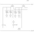
도 1은 본 발명의 실시 예에 따른 박막 트랜지스터 기판의 제n 화소 영역을 표시한 등가 회로도이다.1 is an equivalent circuit diagram illustrating an n-th pixel region of a TFT substrate according to an exemplary embodiment of the present invention.
도 1을 참조하면, 화소 영역은 제1 부화소 영역(P1), 제2 부화소 영역(P2), 제n 게이트 라인(GLn)과 제m 데이터 라인(DLm)에 연결된 제1 및 제2 박막 트랜지스터(Tn1,Tn2)를 포함한다. 그리고, 화소 영역은 제n+1 게이트 라인(GLn+1)과 접속된 제3 박막 트랜지스터(Tn3)와, 제3 박막 트랜지스터(Tn3)에 연결되어 제1 부화소 영역(P1)에 충전되는 전압과 제2 부화소 영역(P2)에 충전되는 전압을 조절하는 전압 업 커패시터(Cup)와 전압 다운 커패시터(Cdown)를 포함한다.1, the pixel region includes a first and a second thin film connected to the first sub-pixel region P1, the second sub-pixel region P2, the n-th gate line GLn and the m-th data line DLm, And transistors Tn1 and Tn2. The pixel region includes a third thin film transistor Tn3 connected to the (n + 1) th gate line GLn + 1 and a third thin film transistor Tn2 connected to the third thin film transistor Tn3, And a voltage down capacitor Cdown for adjusting a voltage charged in the second sub pixel area P2 and a voltage up capacitor Cup and a voltage down capacitor Cdown.
제1 부화소 영역(P1)은 제1 박막 트랜지스터(Tn1)와 연결된 제1 액정 커패시터(H_Clc) 및 제1 스토리지 커패시터(H_Cst)를 포함한다. 제2 부화소 영역(P2)은 제2 박막 트랜지스터(Tn2)와 연결된 제2 액정 커패시터(L_Clc) 및 제2 스토리지 커패시터(H_Cst)를 포함한다.The first sub-pixel region P1 includes a first liquid crystal capacitor H_Clc and a first storage capacitor H_Cst connected to the first thin film transistor Tn1. The second sub-pixel region P2 includes a second liquid crystal capacitor L_Clc and a second storage capacitor H_Cst connected to the second thin film transistor Tn2.
제1 및 제2 박막 트랜지스터(Tn1,Tn2)는 제n 게이트 라인(GLn) 및 제m 데이터 라인(DLm)에 공통으로 연결된다. 이를 통해, 제1 및 제2 박막 트랜지스터(Tn1,Tn2)는 제n 게이트 라인(GLn)에 게이트 온 전압이 인가되면 동시에 턴-온되고, 제m 데이터 라인(DLm)으로 공급되는 데이터 전압을 동시에 제1 및 제2 부화소 영역(P1,P2)에 공급한다. 이때, 제1 및 제2 부화소 영역(P1,P2)에는 동일한 데이터 전압이 충전된다.The first and second thin film transistors Tn1 and Tn2 are commonly connected to the n-th gate line GLn and the m-th data line DLm. The first and second thin film transistors Tn1 and Tn2 are turned on at the same time when the gate-on voltage is applied to the nth gate line GLn, and the data voltages supplied to the mth data line DLm are simultaneously To the first and second sub-pixel regions P1 and P2. At this time, the same data voltage is charged in the first and second sub-pixel regions P1 and P2.
제3 박막 트랜지스터(Tn3)는 제n+1 게이트 라인(GLn+1)과 제2 박막 트랜지스터(Tn2) 및 전압 다운 커패시터(Cdown)에 연결된다. 이를 통해, 제3 박막 트랜지스터(Tn3)는 제n+1 게이트 라인(GLn+1)에 게이트 온 전압이 인가되면 턴-온되어 전압 다운 커패시터(Cdown)과 차지 쉐어(charge share)를 통해 제2 부화소 영역(P2)의 충전 전압의 레벨을 강하시킨다.The third thin film transistor Tn3 is connected to the (n + 1) th gate line GLn + 1, the second thin film transistor Tn2, and the voltage down capacitor Cdown. Accordingly, when the gate-on voltage is applied to the (n + 1) -th gate line GLn + 1, the third thin film transistor Tn3 is turned on so that the voltage of the second thin film transistor Tn3 through the voltage down capacitor Cdown and the charge share The level of the charging voltage of the sub pixel region P2 is lowered.
이를 통해, 제1 부화소 영역(P1)에 충전된 전압과 제2 부화소 영역(P2)에 충전된 전압은 서로 다른 값을 갖게 된다. 여기서, 제2 부화소 영역(P2)에 충전되는 전압은 제1 부화소 영역(P1)에 충전되는 전압보다 더 낮은 레벨의 전압 실효값을 갖는다. 이때, 화소 영역의 측면 시인성을 더욱 향상시키기 위해 제1 부화소 영역(P1)에 충전되는 전압의 레벨을 상승시킬 수 있다. 이를 위해, 제1 부화소 영역(P1)에 충전되는 전압 레벨을 상승시키는 전압 업 커패시터(Cup)가 형성된다.Accordingly, the voltage charged in the first sub-pixel region P1 and the voltage charged in the second sub-pixel region P2 have different values. Here, the voltage charged in the second sub-pixel region P2 has a voltage effective value lower than the voltage charged in the first sub-pixel region P1. At this time, the level of the voltage charged in the first sub-pixel region P1 can be raised to further improve the lateral visibility of the pixel region. To this end, a voltage up capacitor Cup for raising the voltage level charged in the first sub-pixel region P1 is formed.
전압 업 커패시터(Cup)는 전압 다운 커패시터(Cdown)와 제1 박막 트랜지스터(Tn1)와 연결된다. 여기서, 전압 업 커패시터(Cup)는 전압 다운 커패시터(Cdown)와의 차지 쉐어를 통해 제1 부화소 영역(P1)의 충전 전압의 레벨을 상승시킨다.The voltage up capacitor Cup is connected to the voltage down capacitor Cdown and the first thin film transistor Tn1. Here, the voltage up capacitor Cup raises the level of the charge voltage of the first sub-pixel region P1 through the charge sharing with the voltage down capacitor Cdown.
이하에서는 도 2 및 도 3을 참조하여 본 발명의 일 실시 예에 따른 박막 트랜지스터 기판을 상세하게 설명한다.Hereinafter, the thin film transistor substrate according to one embodiment of the present invention will be described in detail with reference to FIGS. 2 and 3. FIG.
도 2는 본 발명의 일 실시 예에 따른 박막 트랜지스터 기판의 화소 영역을 설명하기 위해 도시한 평면도이고, 도 3은 도 2에 도시된 지시선 I-I'선을 따라 박 막 트랜지스터 기판을 절단한 단면을 도시한 단면도이다.FIG. 2 is a plan view illustrating a pixel region of a thin film transistor substrate according to an embodiment of the present invention. FIG. 3 is a cross-sectional view taken along the leader line I-I ' Fig.
도 2 및 도 3을 참조하면, 본 발명의 실시 예에 따른 박막 트랜지스터 기판(100)은 절연 기판(110), 게이트 라인(120a,120b), 스토리지 라인(125), 대향 전극(126), 데이터 라인(160), 제1 및 제2 박막 트랜지스터(Tn1,Tn2), 제1 및 제2 부화소 전극(191,192), 제3 박막 트랜지스터(Tn3) 및 제1 보조 전극(193)을 포함한다.2 and 3, a thin
구체적으로, 절연 기판(110)은 투명한 유리 또는 플라스틱 등의 절연 재질로 형성된다.Specifically, the
상기 게이트 라인(120a,120b)은 절연 기판(110)의 가로 방향으로 연장되어 복수개가 형성된다.The
상기 스토리지 라인(125)은 게이트 라인(120a,120b) 사이에서 게이트 라인(120a,120b)과 동일층에 형성된다. 여기서, 스토리지 라인(125)은 화소 영역에서 다양한 형태로 형성될 수 있다. 예를 들어, 스토리지 라인(125)은 데이터 라인(160)에 인접하여 평행하게 형성되는 세로부와, 세로부를 연결하는 "<" 형태의 사선부와, 게이트 라인(120a,120b)에 인접하여 세로부를 연결하는 확장부를 포함할 수 있다.The
상기 대향 전극(126)은 스토리지 라인(125)과 전기적으로 연결도록 스토리지 라인(125)의 일부분에 형성된다.The
상기 데이터 라인(160)은 게이트 라인(120a,120b)과 수직하게 형성되며, 게이트 절연막(130)에 의해 절연된다.The
상기 제1 박막 트랜지스터(Tn1)는 제1 게이트 전극(121), 제1 반도체층(141), 제1 오믹 접촉층(151), 제1 소스 전극(161) 및 제1 드레인 전극(162)을 포함한다. 상기 제2 박막 트랜지스터(Tn2)는 제2 게이트 전극(122), 제2 반도체층(142), 제2 오믹 접촉층(152), 제2 소스 전극(163) 및 제2 드레인 전극(164)을 포함한다.The first thin film transistor Tn1 includes a
여기서, 제1 게이트 전극(121)과 제2 게이트 전극(122)은 공통으로 게이트 라인(120a)과 연결될 수 있다. 그리고, 게이트 절연막(130)의 상부에 제1 및 제2 게이트 전극(122) 각각과 중첩되게 제1 및 제2 반도체층(141,142)이 형성된다. 이때, 제1 및 제2 반도체층(141,142)은 아몰포스 실리콘(a-Si)으로 형성될 수 있다. 그리고, 제1 및 제2 반도체층(141,142)은 폴리 실리콘(p-Si)으로 형성될 수도 있다. 제1 및 제2 오믹 접촉층(151,152)은 제1 및 제2 반도체층(141,142)의 위에 도핑된 아몰포스 실리콘으로 형성될 수 있다.Here, the
제1 및 제2 소스 전극(161,163)은 제1 및 제2 반도체층(141,142) 위에 데이터 라인(160)과 연결되게 형성된다. 이때, 제2 소스 전극(163)은 제1 소스 전극(161)과 서로 인접하게 형성될 수 있다. 제1 및 제2 소스 전극(161,163) 각각은 제1 및 제2 게이트 전극(122)과 중첩되도록 형성될 수 있다.The first and
제1 드레인 전극(162)은 제1 소스 전극(161)과 마주하여 형성되고, 제1 오믹 접촉층(151)을 통해 제1 반도체층(141)과 연결된다. 그리고, 제1 드레인 전극(162)은 제1 컨택홀(181)을 통해 제1 부화소 전극(191)과 연결된다. 제2 드레인 전극(164)은 제2 소스 전극(163)과 마주하여 형성되고, 제2 오믹 접촉층(152)을 통 해 제2 반도체층(142)과 연결된다. 그리고, 제2 드레인 전극(164)은 제2 컨택홀(182)을 통해 제2 부화소 전극(192)과 연결된다.The
상기 제3 박막 트랜지스터(Tn3)는 제3 게이트 전극(123), 제3 반도체층(143), 제3 오믹 접촉층(153), 제3 소스 전극(165) 및 제3 드레인 전극(166)을 포함한다.The third thin film transistor Tn3 includes a
제3 게이트 전극(123)은 다음단 게이트 라인(120b)에 연결된다. 이때, 제3 게이트 전극(123)은 개구율의 저하를 방지하기 위하여 다음단 게이트 라인(120b)을 직접 사용할 수 있다. 제3 반도체층(143)은 게이트 절연막(130) 위에 제3 게이트 전극(123)과 중첩되게 형성된다. 제3 반도체층(143)은 아몰포스 실리콘(a-Si) 또는 폴리 실리콘(p-Si)을 사용할 수 있다.The
제3 소스 전극(165)은 제3 게이트 전극(123) 및 제3 반도체층(143)과 중첩되게 형성된다. 그리고, 제3 소스 전극(165)은 제3 오믹 접촉층(153)을 통해 제3 반도체층(143)과 연결되며, 제3 컨택홀(183)을 통해 제2 부화소 전극(192)과 접속된다. 제3 드레인 전극(166)은 제3 소스 전극(165)과 마주하여 형성되며, 제3 게이트 전극(123) 및 제3 반도체층(143)과 중첩되게 형선된다. 그리고, 제3 드레인 전극(166)은 제1 부화소 전극(191)과 중첩되게 형성된다. 그리고, 제3 드레인 전극(166)은 제4 컨택홀(184)을 통해 제1 보조 전극(193)과 접속된다.The
보호막(171,172)은 게이트 절연막(130), 데이터 라인(160), 제1 내지 제3 소스 전극(165) 및 제1 내지 제3 드레인 전극(166) 위에 형성된다. 여기서, 보호막(171,172)은 무기 물질로 형성된 무기 보호막(171)과, 유기 물질로 형성된 유기 보호막(172)을 포함한다. 이와 같은 보호막(171,172)은 무기 보호막(171)과 유기 보호막(172)을 적층시켜 제1 내지 제3 박막 트랜지스터(Tn1,Tn2,Tn3)를 보호하고, 오프 특성을 향상시키며 개구율을 향상시킬 수 있다. 이때, 보호막(171,172)은 무기 보호막(171)만으로 형성될 수도 있다.The
상기 제1 부화소 전극(191)은 보호막(171,172) 위에 형성되며, 제1 컨택홀(181)을 통해 제1 드레인 전극(162)과 연결된다. 그리고, 제1 부화소 전극(191)은 스토리지 라인(125)과 적어도 일부분이 중첩되게 형성되어 제1 스토리지 커패시터(H_Cst)를 형성한다. 제1 부화소 전극(191)은 투명한 도전 물질인 인듐 주석 산화물(Indium Tin Oxide: 이하 ITO), 인듐 아연 산화물(Indium Zinc Oxide: 이하 IZO), 인듐 주석 아연 산화물(Indium Tin Zinc Oxide: 이하 ITZO) 등을 사용하여 형성될 수 있다. 이때, 제1 부화소 전극(191)은 화소 영역 내에서 "<" 형태로 형성될 수 있다.The first
여기서, 제1 부화소 전극(191)은 보호막(171,172)을 사이에 두고 제3 드레인 전극(166)과 적어도 일부분이 중첩되어 전압 업 커패시터(Cup)를 형성한다. 이때, 제1 부화소 전극(191)은 제3 드레인 전극(166)과 전기적으로 연결되고 제3 드레인 전극(166)과 동일층에 형성되는 드레인 전극 패턴과 적어도 일부분이 중첩되어 전압 업 커패시터(Cup)를 형성할 수도 있다.Here, the first
상기 제2 부화소 전극(192)은 보호막(171,172) 위에 형성되며, 제2 컨택홀(182)을 통해 제2 드레인 전극(164)과 연결되고, 제3 컨택홀(183)을 통해 제3 소스 전극(165)과 연결된다. 그리고, 제2 부화소 전극(192)은 스토리지 라인(125)과 적어도 일부분이 중첩되게 형성되어 제2 스토리지 커패시터(L_Cst)를 형성한다. 여기서, 제2 부화소 전극(192)은 제1 부화소 전극(191)과 마찬가지로 투명한 도전 물질인 ITO, IZO, ITZO 등으로 형성될 수 있다. 이때, 제2 부화소 전극(192)은 화소 영역 내에서 "<" 형태로 형성될 수 있다.The second
여기서, 제1 및 제2 부화소 전극(191,192)은 절개부(194)를 통해 분할된다. 이때, 절개부(194)는 스토리지 라인(125)과 중첩되게 형성됨으로써 절개부(194)에서 발생되는 빛샘을 방지할 수 있다. 그리고, 제1 및 제2 부화소 전극(191,192)은 도 2에 도시된 바와 같이 "<" 형태의 쉐브론(Chevron) 형태로 형성되는 것에 한정되지 않고, "+" 형태, "X" 형태 등 다양하게 형성될 수 있다.Here, the first and second
상기 제1 보조 전극(193)은 보호막(171,172) 위에 형성되며, 제4 컨택홀(184)을 통해 제3 드레인 전극(166)과 연결된다. 그리고, 제1 보조 전극(193)은 대향 전극(126)과 적어도 일부분이 중첩되게 형성되어, 전압 다운 커패시터(Cdown)를 형성할 수 있다.The first
한편, 도 3에 도시된 박막 트랜지스터 기판에서 제1 내지 제3 반도체층(141,142,143) 및 제1 내지 제3 오믹 접촉층(151,152,153)은 데이터 라인(160), 제1 내지 제3 소스 전극(161,163,165) 및 제1 내지 제3 드레인 전극(162,164,166)과 한 마스크를 통해 형성되므로 채널 영역을 제외한 나머지 영역에서 이들의 하부에 중첩되어 형성된다.3, the first to third semiconductor layers 141, 142, and 143 and the first to third ohmic contact layers 151, 152, and 153 are formed on the
이하에서는 도 4 및 도 5를 참조하여 본 발명의 다른 실시 예에 따른 박막 트랜지스터 기판을 상세하게 설명한다.Hereinafter, a thin film transistor substrate according to another embodiment of the present invention will be described in detail with reference to FIGS. 4 and 5. FIG.
도 4는 본 발명의 다른 실시 예에 따른 박막 트랜지스터 기판의 화소 영역을 설명하기 위해 도시한 평면도이고, 도 5는 도 4에 도시된 지시선 I-I'선을 따라 박막 트랜지스터 기판을 절단한 단면을 도시한 단면도이다.FIG. 4 is a plan view illustrating a pixel region of a thin film transistor substrate according to another embodiment of the present invention, FIG. 5 is a cross-sectional view of a thin film transistor substrate taken along a leader line I-I ' Fig.
도 4 및 도 5를 참조하면, 본 발명의 다른 실시 예에 따른 박막 트랜지스터 기판(100)은 절연 기판(110), 게이트 라인(120a,120b), 스토리지 라인(125), 대향 전극(126), 데이터 라인(160), 제1 및 제2 박막 트랜지스터(Tn1,Tn2), 제1 및 제2 부화소 전극(191,192), 제3 박막 트랜지스터(Tn3), 제1 보조 전극(193) 및 제2 보조 전극(127)을 포함한다.4 and 5, a thin
상기 대향 전극(126)은 스토리지 라인(125)과 전기적으로 연결되도록 스토리지 라인(125)의 일부분에 형성된다.The
상기 제1 부화소 전극(191)은 보호막(171,172) 위에 형성되며, 제1 컨택홀(181)을 통해 제1 드레인 전극(162)과 연결된다.The first
상기 제1 보조 전극(193)은 제4 컨택홀(184)을 통해 제3 드레인 전극(166)과 연결되며, 제5 컨택홀(185)을 통해 제2 보조 전극(127)과 연결된다. 여기서, 제1 보조 전극(193)은 적어도 하나 이상의 절연층을 사이에 두고 대향 전극(126)과 적어도 일부분이 중첩되게 형성된다. 예를 들어, 제1 보조 전극(193)은 게이트 절연막(130) 및 보호막(171,172)을 사이에 두고 대향 전극(126)과 적어도 일부분이 중첩되어 전압 다운 커패시터(Cdown)를 형성한다.The first
상기 제2 보조 전극(127)은 스토리지 라인(125)과 동일층에 제1 보조 전 극(193)과 전기적으로 연결되어 형성된다. 그리고, 제2 보조 전극(127)은 게이트 절연막(130) 및 보호막(171,172)을 사이에 두고 제1 부화소 전극(191)과 적어도 일부분이 중첩되어 전압 업 커패시터(Cup)을 형성한다. 이에 따라, 제2 보조 전극(127)은 전압 다운 커패시터(Cdown)의 충전 전압과 전압 업 커패시터(Cup)의 충전 전압 간의 차지 쉐어를 유도할 수 있다.The second
여기서, 도 5에 도시된 박막 트랜지스터 기판에서 제1 내지 제3 반도체층(141,142,143) 및 제1 내지 제3 오믹 접촉층(151,152,153)은 데이터 라인(160), 제1 내지 제3 소스 전극(161,163,165) 및 제1 내지 제3 드레인 전극(162,164,166)과 한 마스크를 통해 형성되므로 채널 영역을 제외한 나머지 영역에서 이들의 하부에 중첩되어 형성된다.5, the first to third semiconductor layers 141, 142 and 143 and the first to third ohmic contact layers 151, 152 and 153 are formed on the
한편, 도 4 및 도 5에 도시된 구성 요소 중 도 2 및 도 3에 도시된 구성 요소와 동일한 구성 요소는 중복된 설명을 생략한다.4 and FIG. 5, the same elements as those shown in FIGS. 2 and 3 are not described again.
이하에서는 도 6 내지 도 9b를 참조하여 본 발명의 일 실시 예에 따른 박막 트랜지스터 기판의 제조 방법에 대해 상세하게 설명한다.Hereinafter, a method for fabricating a thin film transistor substrate according to an embodiment of the present invention will be described in detail with reference to FIGS. 6 to 9B.
도 6 내지 도 9b는 도 3에 도시된 박막 트랜지스터 기판의 제조 방법을 마스크 공정별로 도시한 단면도이다.6 to 9B are cross-sectional views illustrating a method of manufacturing the thin film transistor substrate shown in FIG. 3 according to a mask process.
도 6은 제1 마스크 공정으로 제1 패턴군이 형성된 것을 도시한 단면도이다.6 is a cross-sectional view showing the first pattern group formed by the first mask process.
도 6을 참조하면, 제1 마스크 공정으로 게이트 라인, 제1 내지 제3 게이트 전극(123), 스토리지 라인(125) 및 대향 전극(126)을 포함하는 게이트 패턴을 형성 한다.Referring to FIG. 6, a gate pattern including a gate line, first to
구체적으로, 절연 기판(110) 위에 스퍼터링 방법 등을 통해 게이트 금속층을 형성한다. 여기서, 게이트 금속층은 몰리브덴(Mo), 알루미늄(Al), 크롬(Cr), 구리(Cu) 등의 단일 금속 또는 이들의 합금을 사용할 수 있다. 이때, 게이트 금속층은 단일층 또는 복층 구조로 형성할 수 있다.Specifically, a gate metal layer is formed on the insulating
다음으로, 제1 마스크를 이용한 포토리소그래피 공정 및 식각 공정으로 게이트 금속층을 패터닝하여 게이트 라인, 제1 내지 제3 게이트 전극(121,122,123), 스토리지 라인(125) 및 대향 전극(126)을 포함하는 게이트 패턴을 형성한다.Next, a gate metal layer is patterned by a photolithography process and an etching process using the first mask to form a gate pattern including a gate line, first to
도 7은 제2 마스크 공정으로 데이터 패턴이 형성된 것을 도시한 단면도이다.7 is a cross-sectional view showing a data pattern formed by the second mask process.
도 7을 참조하면, 게이트 패턴이 형성된 절연 기판(110) 위에 게이트 절연막(130), 아몰포스 실리콘 및 불순물 도핑된 아몰포스 실리콘층을 플라즈마 강화 화학 기상 증착(Plasma Enhanced Chemical Vapor Deposition: 이하 PECVD), 화학 기상 증착(Chemical Vapor Deposition: 이하 CVD) 등의 증착 방법 등을 통해 순차적으로 적층시킨다. 다음으로, 불순물 도핑된 아몰포스 실리콘층 위에 스퍼터링 등의 증착 방법 등을 통해 데이터 금속층을 형성한다.7, a
여기서, 게이트 절연막(130)은 질화 실리콘(SiNx) 또는 산화 실리콘(SiOx) 등을 사용한다. 그리고 데이터 금속층은 몰리브덴(Mo), 알루미늄(Al), 크롬(Cr), 구리(Cu) 등의 단일 금속 또는 이들의 합금을 사용한다. 이때, 데이터 금속층은 단일층 또는 복층 구조로 형성할 수 있다.Here, the
다음으로, 포토레지스트를 도포한 후 제2 마스크를 이용한 포토리소그라피 공정으로 단차를 이루는 포토레지스트 패턴을 형성한다. 여기서, 포토레지스트 패턴은 제1 내지 제3 박막 트랜지스터(Tn1,Tn2,Tn3)의 채널이 형성될 영역에 포토레지스트의 일부가 남겨지고, 데이터 패턴이 형성될 영역에는 포토레지스트의 전량이 남겨지며, 나머지 부분은 포토레지스트가 제거된다.Next, after the photoresist is applied, a photoresist pattern forming a step is formed by a photolithography process using a second mask. Here, in the photoresist pattern, a part of the photoresist is left in the region where the channels of the first to third thin film transistors Tn1, Tn2, and Tn3 are to be formed, the entire amount of the photoresist is left in the region where the data pattern is to be formed, The remaining portion of the photoresist is removed.
다음으로, 제1 식각 공정을 통해 화소 영역의 데이터 금속층을 식각하고, 제2 식각 공정으로 불순물 도핑된 아몰포스 실리콘층 및 아몰포스 실리콘층을 식각한다. 그리고, 애싱 공정을 통해 동일한 깊이로 포토레지스트를 제거한다. 그리고, 제3 식각 공정을 통해 채널 영역의 불순물 도핑된 아몰포스 실리콘을 제거하고, 남겨진 포토 레지스트를 제거하여 데이터 라인, 제1 내지 제3 소스 전극(161,163,165) 및 제1 내지 제3 드레인 전극(162,164,166)을 포함하는 데이터 패턴을 형성한다. 이때, 데이터 패턴의 하부에는 제1 내지 제3 반도체층(141,142,143) 및 제1 내지 제3 오믹 콘택층(151,152,153)이 형성된다.Next, the data metal layer of the pixel region is etched through the first etching process, and the impurity-doped amorphous silicon layer and the amorphous silicon layer are etched by the second etching process. Then, the photoresist is removed to the same depth through an ashing process. Then, the impurity-doped amorphous silicon in the channel region is removed through the third etching process and the remaining photoresist is removed to remove the data line, the first to
도 8a 및 도 8b는 제3 마스크 공정으로 보호막이 형성된 것을 도시한 단면도이다.8A and 8B are cross-sectional views showing a protective film formed in the third mask process.
도 8a 및 도 8b를 참조하면, 두 가지 방법으로 제3 마스크 공정을 통해 제1 내지 제4 컨택홀(181,182,183,184)을 포함하는 보호막(171,172)을 형성한다.Referring to FIGS. 8A and 8B, the
우선, 첫번째 방법은 도 8a에 도시된 바와 같이 데이터 패턴이 형성된 절연 기판(110) 위에 무기 물질을 PECVD, CVD 등의 증착 방법을 통해 증착한다. 그리 고, 제3 마스크를 이용한 포토리소그라피 공정 및 식각 공정으로 제1 내지 제4 컨택홀(181,182,183,184)을 포함하는 무기 보호막(171)을 형성한다.First, as shown in FIG. 8A, an inorganic material is deposited on an insulating
다음으로, 두번째 방법은 도 8b에 도시된 바와 같이 무기 물질을 증착한 뒤 유기 물질을 더 증착한다. 그리고, 제3 마스크를 이용한 포토리소그라피 공정 및 식각 공정으로 제1 내지 제4 컨택홀(181,182,183,184)을 포함하는 무기 보호막(171) 및 유기 보호막(172)을 형성한다.Next, the second method deposits an inorganic material as shown in FIG. 8B and further deposits an organic material. Then, the inorganic
도 9a 및 도 9b는 제4 마스크 공정으로 제1 및 제2 부화소 전극과 보조 전극이 형성된 것을 도시한 단면도이다.9A and 9B are cross-sectional views showing the first and second sub-pixel electrodes and the auxiliary electrode formed in the fourth mask process.
도 9a 및 도 9b를 참조하면, 제4 마스크 공정을 통해 제1 부화소 전극(191), 제2 부화소 전극(192) 및 제1 보조 전극(193)을 포함하는 화소 전극 패턴을 형성한다.Referring to FIGS. 9A and 9B, a pixel electrode pattern including the first
우선, 도 9a 및 도 9b에 도시된 바와 같이 무기 보호막(171) 또는 유기 보호막(172) 위에 ITO, IZO, ITZO 등의 투명 도전 물질을 스퍼터링 등의 증착 방법을 통해 증착한다. 그리고, 제4 마스크를 이용한 포토리소그라피 공정 및 식각 공정을 통해 제1 및 제2 부화소 전극(191,192)과 제1 보조 전극(193)을 패터닝한다. 이때, 제1 및 제2 부화소 전극(191,192)은 절개부(194)에 의해 서로 분리되도록 형성한다.First, as shown in FIGS. 9A and 9B, a transparent conductive material such as ITO, IZO, or ITZO is deposited on the inorganic
구체적으로, 제1 부화소 전극(191)은 도 9a에 도시된 바와 같이 무기 보호막(171)을 사이에 두고 제3 드레인 전극(166)과 중첩되게 형성한다. 이에 따라, 제1 부화소 전극(191)은 제3 드레인 전극(166)과 전압 업 커패시터(Cup)를 형성한다. 한편, 제1 부화소 전극(191)은 도 9b에 도시된 바와 같이 무기 보호막(171) 및 유기 보호막(172)을 사이에 두고 제3 드레인 전극(166)과 적어도 일부분이 중첩되게 형성하여 전압 업 커패시터(Cup)을 형성할 수도 있다.Specifically, the first
제2 부화소 전극(192)은 제2 및 제3 컨택홀(182,183)을 통해 제2 드레인 전극(164) 전극과 제3 소스 전극(165)을 전기적으로 연결하도록 형성한다.The second
제1 보조 전극(193)은 제4 컨택홀(184)을 통해 제3 드레인 전극(166)에 접속되게 형성한다. 여기서, 제1 보조 전극(193)은 도 9a에 도시된 바와 같이 게이트 절연막(130) 및 무기 보호막(171)을 사이에 두고 대향 전극(126)과 적어도 일부분이 중첩되게 형성한다. 이에 따라, 제1 보조 전극(193)은 대향 전극(126)과 전압 다운 커패시터(Cdown)를 형성한다. 그리고, 제1 보조 전극(193)은 도 9b에 도시된 바와 같이 게이트 절연막(130), 무기 보호막(171) 및 유기 보호막(172)을 사이에 두고 대향 전극(126)과 적어도 일부분이 중첩되게 형성하여 전압 다운 커패시터(Cdown)를 형성할 수도 있다.The first
이하에서는 도 10 내지 도 13b를 참조하여 본 발명의 다른 실시 예에 따른 박막 트랜지스터 기판의 제조 방법에 대해 설명한다.Hereinafter, a method for fabricating a thin film transistor substrate according to another embodiment of the present invention will be described with reference to FIGS. 10 to 13B.
도 10 내지 도 13b는 도 5에 도시된 박막 트랜지스터 기판의 제조 방법을 마스크 공정별로 도시한 단면도이다.FIGS. 10 to 13B are cross-sectional views illustrating the method of manufacturing the thin film transistor substrate shown in FIG.
도 10은 제1 마스크 공정으로 제1 패턴군이 형성된 것을 도시한 단면도이다.10 is a cross-sectional view showing the first pattern group formed by the first mask process.
도 10을 참조하면, 제1 마스크 공정으로 게이트 라인, 제1 내지 제3 게이트 전극(121,122,123), 스토리지 라인(125), 대향 전극(126) 및 제2 보조 전극(127)을 포함하는 게이트 패턴을 형성한다.10, a gate pattern including gate lines, first to
구체적으로, 절연 기판(110) 위에 스퍼터링 방법 등을 통해 게이트 금속층을 형성한다. 그리고, 제1 마스크를 이용한 포토리소그래피 공정 및 식각 공정으로 게이트 금속층을 패터닝하여 게이트 라인, 제1 내지 제3 게이트 전극(121,122,123), 스토리지 라인(125), 대향 전극(126) 및 제2 보조 전극(127)을 포함하는 게이트 패턴을 형성한다.Specifically, a gate metal layer is formed on the insulating
도 11은 제2 마스크 공정으로 데이터 패턴이 형성된 것을 도시한 단면도이다.11 is a cross-sectional view showing a data pattern formed in the second mask process.
도 11을 참조하면, 게이트 패턴이 형성된 절연 기판(110) 위에 게이트 절연막(130), 아몰포스 실리콘 및 불순물 도핑된 아몰포스 실리콘층을 순차적으로 적층시킨다. 다음으로, 불순물 도핑된 아몰포스 실리콘층 위에 데이터 금속층을 적층한다. 다음으로, 포토레지스트를 도포한 후 제2 마스크를 이용한 포토리소그라피 공정으로 단차를 이루는 포토레지스트 패턴을 형성한다. 다음으로, 데이터 금속층, 불순물 도핑된 아몰포스 실리콘층 및 아몰포스 실리콘층을 식각하여 데이터 라인, 제1 내지 제3 소스 전극(161,163,165) 및 제1 내지 제3 드레인 전극(162,164,166)을 포함하는 데이터 패턴을 형성한다. 여기서, 제3 드레인 전극(166)은 후술될 제1 부화소 전극과 중첩되지 않도록 형성한다.Referring to FIG. 11, a
도 12a 및 도 12b는 제3 마스크 공정으로 보호막이 형성된 것을 도시한 단면도이다.12A and 12B are cross-sectional views showing a protective film formed by a third mask process.
도 12a 및 도 12b를 참조하면, 두 가지 방법으로 제3 마스크 공정을 통해 제1 내지 제5 콘택홀(181,182,183,184,185)을 포함하는 보호막(171,172)을 형성한다.Referring to FIGS. 12A and 12B,
우선, 첫번째 방법은 도 12a에 도시된 바와 같이 데이터 패턴이 형성된 절연 기판(110) 위에 무기 물질을 PECVD, CVD 등의 증착 방법을 통해 증착한다. 그리고, 제3 마스크를 이용한 포토리소그라피 공정 및 식각 공정으로 제1 내지 제5 콘택홀(181,182,183,184,185)을 포함하는 무기 보호막(171)을 형성한다.First, as shown in FIG. 12A, an inorganic material is deposited on an insulating
다음으로, 두번째 방법은 도 12b에 도시된 바와 같이 무기 물질을 증착한 뒤 유기 물질을 더 증착한다. 그리고, 제3 마스크를 이용한 포토리소그라피 공정 및 식각 공정으로 제1 내지 제5 콘택홀(181,182,183,184,185)을 포함하는 무기 보호막(171) 및 유기 보호막(172)을 형성한다.Next, the second method deposits an inorganic material as shown in FIG. 12B and further deposits an organic material. Then, the inorganic
도 13a 및 도 13b는 제4 마스크 공정으로 제1 및 제2 부화소 전극과 보조 전극이 형성된 것을 도시한 단면도이다.13A and 13B are cross-sectional views illustrating formation of first and second sub-pixel electrodes and an auxiliary electrode in a fourth mask process.
도 13a 및 도 13b를 참조하면, 제4 마스크 공정을 통해 제1 부화소 전극(191), 제2 부화소 전극(192) 및 제1 보조 전극(193)을 포함하는 화소 전극 패턴을 형성한다.Referring to FIGS. 13A and 13B, a pixel electrode pattern including a first
우선, 도 13a 및 도 13b에 도시된 바와 같이 무기 보호막(171) 또는 유기 보 호막(172) 위에 ITO, IZO, ITZO 등의 투명 도전 물질을 스퍼터링 등의 증착 방법을 통해 증착한다. 그리고, 제4 마스크를 이용한 포토리소그라피 공정 및 식각 공정을 통해 제1 및 제2 부화소 전극(191,192)과 제1 보조 전극(193)을 패터닝한다. 이때, 제1 및 제2 부화소 전극(191,192)은 절개부(194)에 의해 서로 분리되도록 형성한다.First, as shown in FIGS. 13A and 13B, a transparent conductive material such as ITO, IZO or ITZO is deposited on the inorganic
구체적으로, 제1 부화소 전극(191)은 도 13a에 도시된 바와 같이 무기 보호막(171)을 사이에 두고 제2 보조 전극(127)과 적어도 일부분이 중첩되게 형성한다. 이에 따라, 제1 부화소 전극(191)은 제2 보조 전극(127)과 전압 업 커패시터(Cup)를 형성한다. 한편, 제1 부화소 전극(191)은 도 9b에 도시된 바와 같이 무기 보호막(171) 및 유기 보호막(172)을 사이에 두고 제2 보조 전극(127)과 적어도 일부분이 중첩되게 형성하여 전압 업 커패시터(Cup)을 형성할 수도 있다.Specifically, the first
제2 부화소 전극(192)은 제2 및 제3 컨택홀(182,183)을 통해 제2 드레인 전극(164) 전극과 제3 소스 전극(165)을 전기적으로 연결하도록 형성한다.The second
제1 보조 전극(193)은 도 13a에 도시된 바와 같이 제4 및 제5 컨택홀(184,185)을 통해 제3 드레인 전극(166) 및 제2 보조 전극(127)에 접속되게 형성한다. 여기서, 제1 보조 전극(193)은 도 13a에 도시된 바와 같이 게이트 절연막(130) 및 무기 보호막(171)을 사이에 두고 대향 전극(126)과 중첩되게 형성한다. 이에 따라, 제1 보조 전극(193)은 대향 전극(126)과 전압 다운 커패시터(Cdown)를 형성한다. 그리고, 제1 보조 전극(193)은 도 13b에 도시된 바와 같이 게이트 절연막(130), 무기 보호막(171) 및 유기 보호막(172)을 사이에 두고 대향 전극(126)과 중첩되게 형성하여 전압 다운 커패시터(Cdown)를 형성할 수도 있다.The first
이상에서 상술한 본 발명은 실시 예를 참조하여 설명하였지만, 해당 기술 분야의 숙련된 당업자 또는 해당 기술 분야에 통상의 지식을 갖는 자라면 후술될 특허 청구 범위에 기재된 본 발명의 사상 및 기술 영역으로부터 벗어나지 않는 범위 내에서 본 발명을 다양하게 수정 및 변경시킬 수 있을 것이다. 따라서, 본 발명의 기술적 범위는 명세서의 상세한 설명에 기재된 내용으로 한정되는 것이 아니라 특허청구범위에 의해 정하여져야만 할 것이다.While the present invention has been described in connection with what is presently considered to be practical exemplary embodiments, it is to be understood that the invention is not limited to the disclosed embodiments, but, on the contrary, It will be understood by those skilled in the art that various changes in form and details may be made therein without departing from the spirit and scope of the invention. Therefore, the technical scope of the present invention should not be limited to the contents described in the detailed description of the specification, but should be defined by the claims.
도 1은 본 발명의 실시 예에 따른 박막 트랜지스터 기판의 제n 화소 영역을 표시한 등가 회로도,FIG. 1 is an equivalent circuit diagram showing an n-th pixel region of a thin film transistor substrate according to an embodiment of the present invention,
도 2는 본 발명의 일 실시 예에 따른 박막 트랜지스터 기판의 화소 영역을 설명하기 위해 도시한 평면도,FIG. 2 is a plan view illustrating a pixel region of a thin film transistor substrate according to an exemplary embodiment of the present invention. FIG.
도 3은 도 2에 도시된 지시선 I-I'선을 따라 박막 트랜지스터 기판을 절단한 단면을 도시한 단면도,FIG. 3 is a sectional view showing a cross section of the thin film transistor substrate taken along the leader line I-I 'shown in FIG. 2,
도 4는 본 발명의 다른 실시 예에 따른 박막 트랜지스터 기판의 화소 영역을 설명하기 위해 도시한 평면도,FIG. 4 is a plan view illustrating a pixel region of a TFT according to another embodiment of the present invention. FIG.
도 5는 도 4에 도시된 지시선 I-I'선을 따라 박막 트랜지스터 기판을 절단한 단면을 도시한 단면도,FIG. 5 is a cross-sectional view showing a cross section of the thin film transistor substrate taken along the leader line I-I 'shown in FIG. 4,
도 6 내지 도 9b는 도 3에 도시된 박막 트랜지스터 기판의 제조 방법을 마스크 공정별로 도시한 단면도 및FIGS. 6 to 9B are cross-sectional views illustrating the manufacturing method of the thin film transistor substrate shown in FIG. 3,
도 10 내지 도 13b는 도 5에 도시된 박막 트랜지스터 기판의 제조 방법을 마스크 공정별로 도시한 단면도이다.FIGS. 10 to 13B are cross-sectional views illustrating the method of manufacturing the thin film transistor substrate shown in FIG.
<도면 부호의 간단한 설명>≪ Brief Description of Drawings &
100: 박막 트랜지스터 기판 110: 절연 기판100: thin film transistor substrate 110: insulating substrate
121,122,123: 제1 내지 제3 게이트 전극121, 122, 123: first to third gate electrodes
125: 스토리지 라인 126: 대향 전극125: storage line 126: opposing electrode
127: 독립 전극 130: 게이트 절연막127: independent electrode 130: gate insulating film
141,142,143: 제1 내지 제3 반도체층141, 142, 143: first to third semiconductor layers
151,152,153: 제1 내지 제3 오믹 접촉층151, 152, 153: first to third ohmic contact layers
161,163,165: 제1 내지 제3 소스 전극161, 163, 165: first to third source electrodes
162,164,166: 제1 내지 제3 드레인 전극162, 164, and 166: first to third drain electrodes
171: 무기 보호막 172: 유기 보호막171: inorganic protective film 172: organic protective film
181,182,183,184,185: 제1 내지 제5 콘택홀181, 182, 183, 184, 185: first to fifth contact holes
191,192: 제1 및 제3 부화소 전극191, 192: first and third sub-pixel electrodes
193: 보조 전극 194: 절개부193: auxiliary electrode 194: incision part
Tn1,Tn2,Tn3: 제1 내지 제3 박막 트랜지스터Tn1, Tn2, Tn3: first to third thin film transistors
P1, P2 : 제1 및 제2 부화소 영역P1, P2: first and second sub-pixel regions
Claims (12)
Translated fromKoreanPriority Applications (6)
| Application Number | Priority Date | Filing Date | Title |
|---|---|---|---|
| KR1020070124739AKR101414043B1 (en) | 2007-12-04 | 2007-12-04 | Thin film transistor substrate |
| JP2008265105AJP5329169B2 (en) | 2007-12-04 | 2008-10-14 | Thin film transistor substrate and liquid crystal display device including the same |
| US12/255,908US8026991B2 (en) | 2007-12-04 | 2008-10-22 | Thin film transistor substrate |
| CN2008101778185ACN101452941B (en) | 2007-12-04 | 2008-12-01 | Thin film transistor substrate, LCD containing same and manufacturing method thereof |
| US13/217,054US8330889B2 (en) | 2007-12-04 | 2011-08-24 | Thin film transistor substrate, liquid crystal display having the same, and method of manufacturing the same |
| US13/709,707US8551826B2 (en) | 2007-12-04 | 2012-12-10 | Thin film transistor substrate, liquid crystal display having the same, and method of manufacturing the same |
Applications Claiming Priority (1)
| Application Number | Priority Date | Filing Date | Title |
|---|---|---|---|
| KR1020070124739AKR101414043B1 (en) | 2007-12-04 | 2007-12-04 | Thin film transistor substrate |
Publications (2)
| Publication Number | Publication Date |
|---|---|
| KR20090058099A KR20090058099A (en) | 2009-06-09 |
| KR101414043B1true KR101414043B1 (en) | 2014-07-21 |
Family
ID=40675344
Family Applications (1)
| Application Number | Title | Priority Date | Filing Date |
|---|---|---|---|
| KR1020070124739AActiveKR101414043B1 (en) | 2007-12-04 | 2007-12-04 | Thin film transistor substrate |
Country Status (4)
| Country | Link |
|---|---|
| US (3) | US8026991B2 (en) |
| JP (1) | JP5329169B2 (en) |
| KR (1) | KR101414043B1 (en) |
| CN (1) | CN101452941B (en) |
Families Citing this family (19)
| Publication number | Priority date | Publication date | Assignee | Title |
|---|---|---|---|---|
| KR101542840B1 (en)* | 2008-09-09 | 2015-08-07 | 삼성디스플레이 주식회사 | Thin film transistor substrate and method of fabricating thereof |
| KR101609727B1 (en)* | 2008-12-17 | 2016-04-07 | 삼성디스플레이 주식회사 | Thin film transistor substrate and method of fabricating thereof |
| KR101600887B1 (en)* | 2009-07-06 | 2016-03-09 | 삼성디스플레이 주식회사 | Thin film transistor substrate and method of fabricating thereof |
| US8373814B2 (en)* | 2009-07-14 | 2013-02-12 | Samsung Display Co., Ltd. | Display panel and display panel device including the transistor connected to storage capacitor |
| KR101739574B1 (en)* | 2009-07-14 | 2017-05-25 | 삼성디스플레이 주식회사 | Display panel and display panel device inclduing the same |
| CN102472939A (en)* | 2009-10-21 | 2012-05-23 | 夏普株式会社 | Liquid crystal display device circuit, liquid crystal display device board, and liquid crystal display device |
| JP5852793B2 (en)* | 2010-05-21 | 2016-02-03 | 株式会社半導体エネルギー研究所 | Method for manufacturing liquid crystal display device |
| TWI457674B (en)* | 2011-04-13 | 2014-10-21 | Au Optronics Corp | Pixel array, pixel structure and pixel structure driving method |
| KR101423907B1 (en)* | 2011-11-22 | 2014-07-29 | 엘지디스플레이 주식회사 | Oxide thin film transistor and method of manufacturing the same |
| KR101973584B1 (en)* | 2012-02-10 | 2019-04-30 | 삼성디스플레이 주식회사 | Thin film transistor display panel and liquid crystal display device comprising thereof |
| CN103091923B (en)* | 2013-01-31 | 2015-02-18 | 深圳市华星光电技术有限公司 | Array substrate and liquid crystal display device |
| CN103268048B (en)* | 2013-04-27 | 2015-12-02 | 合肥京东方光电科技有限公司 | A kind of array base palte, display device and driving method |
| CN103558721A (en)* | 2013-11-18 | 2014-02-05 | 京东方科技集团股份有限公司 | Array substrate, display device and drive method of display device |
| TWI526760B (en) | 2014-07-17 | 2016-03-21 | 友達光電股份有限公司 | Liquid-crystal pixel circuit and driving method therefor |
| KR102267126B1 (en)* | 2014-12-19 | 2021-06-21 | 삼성디스플레이 주식회사 | Display panel and method for fabricating the same |
| KR102523911B1 (en)* | 2016-02-05 | 2023-04-20 | 삼성디스플레이 주식회사 | Display device |
| KR102544323B1 (en)* | 2016-11-08 | 2023-06-19 | 삼성디스플레이 주식회사 | Display device |
| KR102263122B1 (en) | 2017-10-19 | 2021-06-09 | 삼성디스플레이 주식회사 | Transistor panel |
| US11435638B2 (en)* | 2018-09-13 | 2022-09-06 | Sakai Display Products Corporation | Liquid crystal display device |
Citations (3)
| Publication number | Priority date | Publication date | Assignee | Title |
|---|---|---|---|---|
| KR20050017371A (en)* | 2003-08-13 | 2005-02-22 | 삼성전자주식회사 | Liquid crystal display having multi domain and panel for the same |
| JP2006276411A (en) | 2005-03-29 | 2006-10-12 | Sharp Corp | Liquid crystal display |
| KR20070079614A (en)* | 2006-02-03 | 2007-08-08 | 삼성전자주식회사 | Liquid Crystal Display and Manufacturing Method Thereof |
Family Cites Families (14)
| Publication number | Priority date | Publication date | Assignee | Title |
|---|---|---|---|---|
| JPH06102537A (en)* | 1992-09-22 | 1994-04-15 | Toshiba Corp | Active matrix liquid crystal display device |
| DE19712233C2 (en)* | 1996-03-26 | 2003-12-11 | Lg Philips Lcd Co | Liquid crystal display and manufacturing method therefor |
| JP3891846B2 (en)* | 2002-01-15 | 2007-03-14 | 株式会社日立製作所 | Liquid crystal display |
| US7205570B2 (en)* | 2002-07-19 | 2007-04-17 | Samsung Electronics Co., Ltd. | Thin film transistor array panel |
| US7206048B2 (en)* | 2003-08-13 | 2007-04-17 | Samsung Electronics Co., Ltd. | Liquid crystal display and panel therefor |
| KR101086477B1 (en)* | 2004-05-27 | 2011-11-25 | 엘지디스플레이 주식회사 | Method for manufacturing thin film transistor substrate for display element |
| JP4571845B2 (en)* | 2004-11-08 | 2010-10-27 | シャープ株式会社 | Substrate for liquid crystal display device, liquid crystal display device including the same, and driving method thereof |
| KR101168728B1 (en)* | 2005-07-15 | 2012-07-26 | 삼성전자주식회사 | Wire and method for fabricating interconnection line and thin film transistor substrate and method for fabricating the same |
| KR20070012081A (en)* | 2005-07-22 | 2007-01-25 | 삼성전자주식회사 | Method of manufacturing thin film transistor substrate |
| KR101171187B1 (en)* | 2005-11-07 | 2012-08-06 | 삼성전자주식회사 | Thin film transistor array panel, manufacturing method thereof, and liquid crystal display including the same |
| KR101295298B1 (en)* | 2006-07-28 | 2013-08-08 | 삼성디스플레이 주식회사 | Liquid crystal display |
| KR20080056493A (en)* | 2006-12-18 | 2008-06-23 | 삼성전자주식회사 | Thin film transistor substrate and manufacturing method thereof |
| US8542227B2 (en)* | 2007-02-05 | 2013-09-24 | Samsung Display Co., Ltd. | Display apparatus and method for driving the same |
| KR101402913B1 (en)* | 2007-07-04 | 2014-06-03 | 삼성디스플레이 주식회사 | Thin film transistor array panel and display appratus having the same |
- 2007
- 2007-12-04KRKR1020070124739Apatent/KR101414043B1/enactiveActive
- 2008
- 2008-10-14JPJP2008265105Apatent/JP5329169B2/enactiveActive
- 2008-10-22USUS12/255,908patent/US8026991B2/enactiveActive
- 2008-12-01CNCN2008101778185Apatent/CN101452941B/enactiveActive
- 2011
- 2011-08-24USUS13/217,054patent/US8330889B2/enactiveActive
- 2012
- 2012-12-10USUS13/709,707patent/US8551826B2/enactiveActive
Patent Citations (3)
| Publication number | Priority date | Publication date | Assignee | Title |
|---|---|---|---|---|
| KR20050017371A (en)* | 2003-08-13 | 2005-02-22 | 삼성전자주식회사 | Liquid crystal display having multi domain and panel for the same |
| JP2006276411A (en) | 2005-03-29 | 2006-10-12 | Sharp Corp | Liquid crystal display |
| KR20070079614A (en)* | 2006-02-03 | 2007-08-08 | 삼성전자주식회사 | Liquid Crystal Display and Manufacturing Method Thereof |
Also Published As
| Publication number | Publication date |
|---|---|
| KR20090058099A (en) | 2009-06-09 |
| JP2009139929A (en) | 2009-06-25 |
| US20090141207A1 (en) | 2009-06-04 |
| JP5329169B2 (en) | 2013-10-30 |
| US8026991B2 (en) | 2011-09-27 |
| US8551826B2 (en) | 2013-10-08 |
| CN101452941B (en) | 2012-07-04 |
| US20130095618A1 (en) | 2013-04-18 |
| US20110310323A1 (en) | 2011-12-22 |
| US8330889B2 (en) | 2012-12-11 |
| CN101452941A (en) | 2009-06-10 |
Similar Documents
| Publication | Publication Date | Title |
|---|---|---|
| KR101414043B1 (en) | Thin film transistor substrate | |
| US8203662B2 (en) | Vertical channel thin-film transistor and method of manufacturing the same | |
| US7212255B2 (en) | Liquid crystal display device and fabricating method thereof | |
| US8035108B2 (en) | Thin film transistor substrate, liquid crystal display panel including the same, and method of manufacturing liquid crystal display panel | |
| US20070170504A1 (en) | Thin film transistor substrate and method of fabricating the same and liquid crystal display having the thin film transistor substrate | |
| US20120161140A1 (en) | Tft array substrate and manufacturing method thereof | |
| US7119368B2 (en) | Thin film transistor array panel and manufacturing method thereof | |
| US20080197356A1 (en) | Thin film transistor substrate and method of manufacturing the same | |
| EP3118675B1 (en) | Ultra high density thin film transistor substrate having low line resistance structure and method for manufacturing the same | |
| KR20170117261A (en) | Liquid crystal display device and method for fabricating the same | |
| US20140131718A1 (en) | Tft array substrate and manufacturing method thereof | |
| JP4703258B2 (en) | Thin film transistor substrate and liquid crystal display panel | |
| US20140078436A1 (en) | Pixel structure for liquid crystal display, array substrate and liquid crystal display | |
| CN100422830C (en) | Thin film transistor array panel | |
| CN114779547B (en) | Display substrate, preparation method thereof and display device | |
| US6861671B2 (en) | Thin film transistor liquid crystal display and fabrication method thereof | |
| US8488093B2 (en) | Array substrate for liquid crystal display and manufacturing method thereof | |
| KR101429921B1 (en) | Liquid crystal display device | |
| KR20090060082A (en) | Liquid crystal display device and manufacturing method thereof | |
| US20050001944A1 (en) | Method of stabilizing parasitic capacitance in an LCD device | |
| KR101136269B1 (en) | Array substrate of liquid crystal display device and manufacturing method therof | |
| KR102000053B1 (en) | Thin film transistor substrate and method for fabricating the same | |
| KR20090070174A (en) | LCD panel and manufacturing method | |
| KR20080014243A (en) | LCD and its manufacturing method | |
| KR20080034603A (en) | Method of manufacturing thin film transistor substrate and liquid crystal display panel having same |
Legal Events
| Date | Code | Title | Description |
|---|---|---|---|
| PA0109 | Patent application | Patent event code:PA01091R01D Comment text:Patent Application Patent event date:20071204 | |
| PG1501 | Laying open of application | ||
| N231 | Notification of change of applicant | ||
| PN2301 | Change of applicant | Patent event date:20120912 Comment text:Notification of Change of Applicant Patent event code:PN23011R01D | |
| A201 | Request for examination | ||
| PA0201 | Request for examination | Patent event code:PA02012R01D Patent event date:20121204 Comment text:Request for Examination of Application Patent event code:PA02011R01I Patent event date:20071204 Comment text:Patent Application | |
| E902 | Notification of reason for refusal | ||
| PE0902 | Notice of grounds for rejection | Comment text:Notification of reason for refusal Patent event date:20131030 Patent event code:PE09021S01D | |
| E701 | Decision to grant or registration of patent right | ||
| PE0701 | Decision of registration | Patent event code:PE07011S01D Comment text:Decision to Grant Registration Patent event date:20140428 | |
| GRNT | Written decision to grant | ||
| PR0701 | Registration of establishment | Comment text:Registration of Establishment Patent event date:20140625 Patent event code:PR07011E01D | |
| PR1002 | Payment of registration fee | Payment date:20140626 End annual number:3 Start annual number:1 | |
| PG1601 | Publication of registration | ||
| FPAY | Annual fee payment | Payment date:20170601 Year of fee payment:4 | |
| PR1001 | Payment of annual fee | Payment date:20170601 Start annual number:4 End annual number:4 | |
| FPAY | Annual fee payment | Payment date:20190529 Year of fee payment:6 | |
| PR1001 | Payment of annual fee | Payment date:20190529 Start annual number:6 End annual number:6 | |
| PR1001 | Payment of annual fee | Payment date:20200527 Start annual number:7 End annual number:7 | |
| PR1001 | Payment of annual fee | Payment date:20210601 Start annual number:8 End annual number:8 | |
| PR1001 | Payment of annual fee | Payment date:20230524 Start annual number:10 End annual number:10 | |
| PR1001 | Payment of annual fee | Payment date:20240523 Start annual number:11 End annual number:11 |