KR101413651B1 - Semiconductor device having transistor and method for manufacturing the same - Google Patents
Semiconductor device having transistor and method for manufacturing the sameDownload PDFInfo
- Publication number
- KR101413651B1 KR101413651B1KR1020080049674AKR20080049674AKR101413651B1KR 101413651 B1KR101413651 B1KR 101413651B1KR 1020080049674 AKR1020080049674 AKR 1020080049674AKR 20080049674 AKR20080049674 AKR 20080049674AKR 101413651 B1KR101413651 B1KR 101413651B1
- Authority
- KR
- South Korea
- Prior art keywords
- region
- gate
- edge
- active region
- delete delete
- Prior art date
- Legal status (The legal status is an assumption and is not a legal conclusion. Google has not performed a legal analysis and makes no representation as to the accuracy of the status listed.)
- Active
Links
Images


Classifications
- H—ELECTRICITY
- H10—SEMICONDUCTOR DEVICES; ELECTRIC SOLID-STATE DEVICES NOT OTHERWISE PROVIDED FOR
- H10D—INORGANIC ELECTRIC SEMICONDUCTOR DEVICES
- H10D64/00—Electrodes of devices having potential barriers
- H10D64/60—Electrodes characterised by their materials
- H10D64/66—Electrodes having a conductor capacitively coupled to a semiconductor by an insulator, e.g. MIS electrodes
- H10D64/671—Electrodes having a conductor capacitively coupled to a semiconductor by an insulator, e.g. MIS electrodes the conductor having lateral variation in doping or structure
- H—ELECTRICITY
- H01—ELECTRIC ELEMENTS
- H01L—SEMICONDUCTOR DEVICES NOT COVERED BY CLASS H10
- H01L21/00—Processes or apparatus adapted for the manufacture or treatment of semiconductor or solid state devices or of parts thereof
- H01L21/02—Manufacture or treatment of semiconductor devices or of parts thereof
- H01L21/04—Manufacture or treatment of semiconductor devices or of parts thereof the devices having potential barriers, e.g. a PN junction, depletion layer or carrier concentration layer
- H01L21/18—Manufacture or treatment of semiconductor devices or of parts thereof the devices having potential barriers, e.g. a PN junction, depletion layer or carrier concentration layer the devices having semiconductor bodies comprising elements of Group IV of the Periodic Table or AIIIBV compounds with or without impurities, e.g. doping materials
- H01L21/28—Manufacture of electrodes on semiconductor bodies using processes or apparatus not provided for in groups H01L21/20 - H01L21/268
- H01L21/28008—Making conductor-insulator-semiconductor electrodes
- H01L21/28017—Making conductor-insulator-semiconductor electrodes the insulator being formed after the semiconductor body, the semiconductor being silicon
- H01L21/28026—Making conductor-insulator-semiconductor electrodes the insulator being formed after the semiconductor body, the semiconductor being silicon characterised by the conductor
- H01L21/28105—Making conductor-insulator-semiconductor electrodes the insulator being formed after the semiconductor body, the semiconductor being silicon characterised by the conductor the final conductor next to the insulator having a lateral composition or doping variation, or being formed laterally by more than one deposition step
- H—ELECTRICITY
- H10—SEMICONDUCTOR DEVICES; ELECTRIC SOLID-STATE DEVICES NOT OTHERWISE PROVIDED FOR
- H10D—INORGANIC ELECTRIC SEMICONDUCTOR DEVICES
- H10D30/00—Field-effect transistors [FET]
- H10D30/01—Manufacture or treatment
- H10D30/021—Manufacture or treatment of FETs having insulated gates [IGFET]
- H10D30/0221—Manufacture or treatment of FETs having insulated gates [IGFET] having asymmetry in the channel direction, e.g. lateral high-voltage MISFETs having drain offset region or extended-drain MOSFETs [EDMOS]
- H—ELECTRICITY
- H10—SEMICONDUCTOR DEVICES; ELECTRIC SOLID-STATE DEVICES NOT OTHERWISE PROVIDED FOR
- H10D—INORGANIC ELECTRIC SEMICONDUCTOR DEVICES
- H10D30/00—Field-effect transistors [FET]
- H10D30/60—Insulated-gate field-effect transistors [IGFET]
- H10D30/601—Insulated-gate field-effect transistors [IGFET] having lightly-doped drain or source extensions, e.g. LDD IGFETs or DDD IGFETs
- H10D30/603—Insulated-gate field-effect transistors [IGFET] having lightly-doped drain or source extensions, e.g. LDD IGFETs or DDD IGFETs having asymmetry in the channel direction, e.g. lateral high-voltage MISFETs having drain offset region or extended drain IGFETs [EDMOS]
- H—ELECTRICITY
- H10—SEMICONDUCTOR DEVICES; ELECTRIC SOLID-STATE DEVICES NOT OTHERWISE PROVIDED FOR
- H10D—INORGANIC ELECTRIC SEMICONDUCTOR DEVICES
- H10D30/00—Field-effect transistors [FET]
- H10D30/60—Insulated-gate field-effect transistors [IGFET]
- H10D30/601—Insulated-gate field-effect transistors [IGFET] having lightly-doped drain or source extensions, e.g. LDD IGFETs or DDD IGFETs
- H10D30/605—Insulated-gate field-effect transistors [IGFET] having lightly-doped drain or source extensions, e.g. LDD IGFETs or DDD IGFETs having significant overlap between the lightly-doped extensions and the gate electrode
- H—ELECTRICITY
- H10—SEMICONDUCTOR DEVICES; ELECTRIC SOLID-STATE DEVICES NOT OTHERWISE PROVIDED FOR
- H10D—INORGANIC ELECTRIC SEMICONDUCTOR DEVICES
- H10D64/00—Electrodes of devices having potential barriers
- H10D64/20—Electrodes characterised by their shapes, relative sizes or dispositions
- H10D64/27—Electrodes not carrying the current to be rectified, amplified, oscillated or switched, e.g. gates
- H10D64/311—Gate electrodes for field-effect devices
- H10D64/411—Gate electrodes for field-effect devices for FETs
- H10D64/511—Gate electrodes for field-effect devices for FETs for IGFETs
- H10D64/517—Gate electrodes for field-effect devices for FETs for IGFETs characterised by the conducting layers
- H10D64/519—Gate electrodes for field-effect devices for FETs for IGFETs characterised by the conducting layers characterised by their top-view geometrical layouts
Landscapes
- Engineering & Computer Science (AREA)
- Physics & Mathematics (AREA)
- Condensed Matter Physics & Semiconductors (AREA)
- General Physics & Mathematics (AREA)
- Manufacturing & Machinery (AREA)
- Computer Hardware Design (AREA)
- Microelectronics & Electronic Packaging (AREA)
- Power Engineering (AREA)
- Insulated Gate Type Field-Effect Transistor (AREA)
- Electrodes Of Semiconductors (AREA)
Abstract
Translated fromKoreanDescription
Translated fromKorean본 발명은 트랜지스터를 구비한 반도체 소자 및 그 제조 방법에 관한 것으로, 특히 소자분리 영역 및 활성 영역에 걸쳐서 연장되는 게이트 전극을 포함하는 트랜지스터를 구비한 반도체 소자 및 그 제조 방법에 관한 것이다.The present invention relates to a semiconductor device having a transistor and a method of manufacturing the same, and more particularly, to a semiconductor device including a transistor including a gate electrode extending over an isolation region and an active region, and a method of manufacturing the same.
액정 디스플레이 장치 (liquid crystal display device: LCD), 플라즈마 디스플레이 장치 (plasma display panel: PDP) 등과 같은 평판 표시장치가 널리 보급됨에 따라, LCD 또는 PDP를 구동하기 위한 디스플레이 구동 집적회로 (display driver IC: DDI)가 활발하게 개발되고 있다. DDI는 약 8 ∼ 200 V 의 높은 전압에서 동작하는 고전압 트랜지스터와 약 5 V 이하의 낮은 전압에서 동작하는 일반 트랜지스터를 구비한다.2. Description of the Related Art Flat panel display devices such as liquid crystal display devices (LCDs) and plasma display panels (PDPs) have become widely popular. Accordingly, display driver ICs (DDI ) Are being actively developed. DDI has a high voltage transistor operating at a high voltage of about 8 to 200 V and a general transistor operating at a low voltage of about 5 V or less.
상기 고전압 트랜지스터는 고전압에서의 접합 항복 전압 (junction breakdown voltage)을 높이기 위해 활성 영역에 형성되는 웰 영역의 불순물 도핑 농도를 일반 트랜지스터에 비해 낮게 한다. 따라서, 활성 영역과 소자분리막과의 계면에 인접한 활성 영역의 에지 부분에서는 웰 영역으로부터 소자분리 영역으로의 도판트 확산으로 인해 웰 영역 내에서의 불순물 농도가 더 낮아진다. 이와 같이 불순물 농도가 낮아진 활성 영역의 에지 부분에서는 활성 영역의 센터 부분에서보다 낮은 전압에서 약한 반전 (weak inversion)이 일어나 기생 (parasitic) 트랜지스터가 형성되고, 이로 인해 게이트 전압 (Vg)에 따른 드레인 전류 (Id)의 응답에서 원하지 않는 험프 (hump) 현상이 나타나는 문제가 있다. 소자분리 영역과 활성 영역과의 계면에 인접한 활성 영역의 에지 부분에서 발생되는 험프 현상으로 인해 누설 전류가 증가하고, 트랜지스터의 컷오프 (cut-off) 특성이 저하된다.The high voltage transistor lowers the impurity doping concentration of the well region formed in the active region compared to a general transistor to increase the junction breakdown voltage at a high voltage. Therefore, the impurity concentration in the well region becomes lower due to dopant diffusion from the well region to the device isolation region at the edge portion of the active region adjacent to the interface between the active region and the device isolation film. In the edge portion of the active region where the impurity concentration is lowered, a weak inversion occurs at a lower voltage in the center portion of the active region, and a parasitic transistor is formed. As a result, a drain current There is a problem that an undesired hump phenomenon appears in the response of Id . The leakage current is increased due to the hump phenomenon occurring at the edge portion of the active region adjacent to the interface between the device isolation region and the active region, and the cut-off characteristic of the transistor is degraded.
본 발명의 목적은 상기한 종래 기술에서의 문제점들을 해결하고자 하는 것으로, 소자분리 영역과 활성 영역과의 계면에 인접한 활성 영역의 에지 부분에서의 기생 트랜지스터로 인해 게이트 전압 (Vg)에 따른 드레인 전류 (Id)의 응답에서 원하지 않는 험프가 발생되는 것을 방지할 수 있는 트랜지스터를 구비한 반도체 소자를 제공하는 것이다.SUMMARY OF THE INVENTION It is an object of the present invention to solve the problems in the prior art described above and to solve the problems in the prior art by providing a semiconductor device having a drain current (Vg) according to a gate voltage (Vg) due to a parasitic transistor at an edge portion of an active region, Id ) which can prevent unwanted hump from occurring in the response of the semiconductor device.
본 발명의 다른 목적은 소자분리 영역과 활성 영역과의 계면에 인접한 활성 영역의 에지 부분에서의 기생 트랜지스터로 인해 게이트 전압 (Vg)에 따른 드레인 전류 (Id)의 응답에서 원하지 않는 험프가 발생되는 것을 방지할 수 있는 트랜지스터를 구비한 반도체 소자의 제조 방법을 제공하는 것이다.Another object of the present invention is that unwanted hump occurs in the response of the drain current (Id) according to the gate voltage (Vg) due to the parasitic transistor at the edge of the active area adjacent to the interface between the device isolation region and the active region And a method of manufacturing a semiconductor device having a transistor capable of preventing a semiconductor device from being deteriorated.
상기 목적을 달성하기 위하며, 본 발명에 따른 반도체 소자는 기판에서 소자분리 영역에 의해 정의되어 있고, 상기 소자분리 영역과의 계면에 인접한 에지 부분과 상기 에지 부분에 의해 포위되는 센터 부분을 포함하는 활성 영역을 포함한다. 상기 활성 영역 및 상기 소자분리 영역 위에 게이트 전극이 형성되어 있으며, 상기 게이트 전극은 상기 활성 영역의 센터 부분을 덮는 센터 게이트 부분과 상기 활성 영역의 에지 부분을 덮는 에지 게이트 부분을 포함한다. 제1 도전형의 제1 불순물 도핑 영역이 상기 센터 게이트 부분에만 형성되어 있다. 상기 활성 영역과 상 기 게이트 전극과의 사이에는 게이트 절연막이 개재되어 있다.In order to achieve the above object, a semiconductor device according to the present invention is defined by an element isolation region in a substrate, and includes an edge portion adjacent to the interface with the element isolation region and a center portion surrounded by the edge portion Active region. A gate electrode is formed on the active region and the device isolation region, and the gate electrode includes a center gate portion covering the center portion of the active region and an edge gate portion covering the edge portion of the active region. A first impurity doped region of the first conductivity type is formed only in the center gate portion. A gate insulating film is interposed between the active region and the gate electrode.
상기 에지 게이트 부분은 불순물로 도핑되어 있지 않을 수 있다. 또는, 상기 에지 게이트 부분은 상기 제1 도전형과 반대인 제2 도전형의 제2 불순물 도핑 영역을 포함할 수 있다.The edge gate portion may not be doped with an impurity. Alternatively, the edge gate portion may include a second impurity doped region of a second conductivity type opposite to the first conductivity type.
본 발명에 따른 반도체 소자는 상기 게이트 전극의 양 측에서 상기 활성 영역에 각각 형성된 소스 영역 및 드레인 영역을 더 포함할 수 있다. 상기 소스 영역 및 드레인 영역은 상기 제1 도전형의 불순물이 도핑되어 있을 수 있다.The semiconductor device according to the present invention may further include a source region and a drain region which are respectively formed in the active region on both sides of the gate electrode. The source region and the drain region may be doped with an impurity of the first conductivity type.
상기 게이트 전극은 상기 제1 불순물 도핑 영역을 사이에 두고 그 양 측에 상기 소자분리 영역까지 각각 연장되어 있는 제1 단부 및 제2 단부를 포함할 수 있다. 상기 에지 게이트 부분은 상기 제1 단부에 형성된 제1 에지 게이트 부분과, 상기 제2 단부에 형성된 제2 에지 게이트 부분을 포함할 수 있다.The gate electrode may include a first end and a second end extending to the element isolation region on both sides of the first impurity doped region. The edge gate portion may include a first edge gate portion formed at the first end and a second edge gate portion formed at the second end.
상기 제1 에지 게이트 부분 및 제2 에지 게이트 부분은 각각 불순물로 도핑되어 있지 않을 수 있다. 또는, 상기 제1 에지 게이트 부분 및 제2 에지 게이트 부분은 각각 상기 제1 도전형과 반대인 제2 도전형의 제2 불순물 도핑 영역을 포함할 수 있다. 이 때, 상기 제1 에지 게이트 부분 및 제2 에지 게이트 부분은 서로 다른 불순물 도핑 농도를 가질 수 있다.The first edge gate portion and the second edge gate portion may not be doped with an impurity, respectively. Alternatively, the first edge gate portion and the second edge gate portion may each include a second impurity doped region of a second conductivity type opposite to the first conductivity type. At this time, the first edge gate portion and the second edge gate portion may have different impurity doping concentrations.
본 발명에 따른 반도체 소자에서, 상기 제1 에지 게이트 부분 및 제2 에지 게이트 부분 중 어느 하나는 불순물로 도핑되어 있지 않고, 상기 제1 에지 게이트 부분 및 제2 에지 게이트 부분 중 다른 하나는 상기 제1 도전형과 반대인 제2 도전형의 제2 불순물 도핑 영역을 포함할 수 있다.In the semiconductor device according to the present invention, one of the first edge gate portion and the second edge gate portion is not doped with an impurity, and the other of the first edge gate portion and the second edge gate portion is the first And a second impurity doped region of the second conductivity type opposite to the conductive type.
본 발명에 따른 반도체 소자의 게이트 전극은 제1 방향에서 상기 제1 불순물 도핑 영역을 사이에 두고 그 양 측에서 상기 소자분리 영역 위에 위치되는 1 쌍의 제1 측벽과, 상기 제1 방향에 수직인 제2 방향에서 상기 제1 불순물 도핑 영역을 사이에 두고 그 양 측에서 상기 활성 영역 위에 위치되는 1 쌍의 제2 측벽을 포함할 수 있다.The gate electrode of the semiconductor device according to the present invention includes a pair of first sidewalls located on the device isolation region on both sides of the first impurity doped region in the first direction, And a pair of second sidewalls located on the active region on both sides of the first impurity doped region in the second direction.
상기 제1 불순물 도핑 영역은 상기 1 쌍의 제1 측벽 및 상기 1 쌍의 제2 측벽으로부터 각각 이격된 위치에 형성될 수 있다.The first impurity doped region may be formed at a position spaced apart from the pair of first sidewalls and the pair of second sidewalls.
상기 다른 목적을 달성하기 위하여, 본 발명에 따른 반도체 소자의 제조 방법에서는 기판에 소자분리 영역을 형성하여 상기 소자분리 영역과의 계면에 인접한 에지 부분과 상기 에지 부분에 의해 포위되는 센터 부분을 포함하는 활성 영역을 정의한다. 상기 활성 영역 위에 게이트 절연막을 형성한다. 상기 활성 영역의 센터 부분 및 에지 부분 위에 연장되고 상기 소자분리막 위에 위치되는 제1 단부를 포함하는 게이트 패턴을 상기 게이트 절연막 위에 형성한다. 상기 게이트 패턴 중 상기 제1 단부를 포함하지 않는 일부 영역에만 제1 도전형의 불순물을 주입하여 상기 활성 영역의 센터 부분 위에서 상기 게이트 패턴 내에 제1 도전형의 제1 불순물 도핑 영역을 형성한다.According to another aspect of the present invention, there is provided a method for fabricating a semiconductor device, comprising: forming a device isolation region on a substrate and including an edge portion adjacent to the interface with the device isolation region and a center portion surrounded by the edge portion; Define the active area. A gate insulating film is formed on the active region. A gate pattern is formed on the gate insulating film, the gate pattern including a center portion and an edge portion of the active region, and a first end located on the isolation film. Impurity of the first conductivity type is implanted only in a part of the gate pattern not including the first end to form a first impurity doped region of the first conductivity type in the gate pattern on the center portion of the active region.
상기 게이트 패턴은 상기 활성 영역 위에 위치되는 제2 단부를 더 포함할 수 있다. 그리고, 상기 제1 불순물 도핑 영역은 상기 제2 단부로부터 이격된 위치에 형성될 수 있다.The gate pattern may further include a second end located above the active region. The first impurity doped region may be formed at a position spaced apart from the second end.
본 발명에 따른 반도체 소자의 제조 방법에서, 상기 게이트 절연막을 형성하 기 전에 상기 활성 영역에 저농도의 제1 도전형 불순물 영역을 형성할 수 있다. 또한, 상기 제1 불순물 도핑 영역 형성과 동시에 상기 저농도의 제1 도전형 불순물 영역 내에 고농도의 제1 도전형 불순물 영역을 형성할 수 있다.In the method of manufacturing a semiconductor device according to the present invention, a low concentration first conductivity type impurity region may be formed in the active region before forming the gate insulating film. In addition, it is possible to form the first conductivity type impurity region at a high concentration in the low concentration first conductivity type impurity region simultaneously with the formation of the first impurity doping region.
본 발명에 따른 반도체 소자의 제조 방법에서, 상기 게이트 패턴의 제1 단부에 상기 제1 도전형과 반대인 제2 도전형의 제2 불순물 도핑 영역을 형성할 수 있다. 상기 제2 불순물 도핑 영역은 상기 제1 불순물 도핑 영역 형성 단계 전에 형성될 수도 있고 상기 제1 불순물 도핑 영역 형성 단계 후에 형성될 수도 있다.In the method of manufacturing a semiconductor device according to the present invention, a second impurity doped region of the second conductivity type opposite to the first conductivity type may be formed at a first end of the gate pattern. The second impurity doped region may be formed before the first impurity doped region forming step or may be formed after the first impurity doped region forming step.
본 발명에 따른 반도체 소자는 게이트 전극의 에지 게이트 부분에는 불순물이 도핑되지 않거나 상기 게이트 전극의 센터 게이트 부분 보다 낮은 농도의 불순물, 또는 센터 게이트 부분과 반대 도전형의 불순물이 도핑되어 있다. 따라서, 소자분리 영역과 활성 영역과의 계면에 인접한 활성 영역의 에지 부분 위에 있는 에지 게이트 부분에서 등가산화막 두께가 증가하는 결과가 얻어지고, 게이트 전극과 기판과의 일함수 (work function) 전위차 (Φms)가 줄어들어, 게이트 전극의 에지 게이트 부분 아래에 있는 활성 영역의 에지 부분에서 한계 전압(Vth)이 커지게 된다. 따라서, 소자분리 영역과 활성 영역과의 계면에 인접한 활성 영역의 에지 부분에서의 기생 트랜지스터로 인해 게이트 전압 (Vg)에 따른 드레인 전류 (Id)의 응답에서 원하지 않는 험프가 발생되는 것을 방지할 수 있다.In the semiconductor device according to the present invention, the edge gate portion of the gate electrode is doped with impurities at a concentration lower than that of the center gate portion of the gate electrode, or an impurity of the opposite conductivity type to the center gate portion. Therefore, the result of the equivalent oxide film thickness increase at the edge gate portion above the edge portion of the active region adjacent to the interface between the element isolation region and the active region is obtained, and the work function potential difference (Φms ) Is reduced, and the threshold voltage (Vth) at the edge portion of the active region below the edge gate portion of the gate electrode becomes large. Therefore, the parasitic transistor at the edge portion of the active region adjacent to the interface between the element isolation region and the active region can prevent the undesired hump from occurring in the response of the drain current Id with respect to the gate voltage Vg have.
다음에, 본 발명의 바람직한 실시예들에 대하여 첨부 도면을 참조하여 상세히 설명한다.Next, preferred embodiments of the present invention will be described in detail with reference to the accompanying drawings.
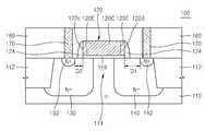
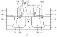
도 1a는 본 발명의 바람직한 실시예에 따른 반도체 소자의 요부 구성을 도시한 레이아웃이다. 도 1b는 도 1a의 Ib - Ib'선 단면도이고, 도 1c는 도 1a의 Ic - Ic'선 단면도이다.BRIEF DESCRIPTION OF THE DRAWINGS FIG. 1A is a layout showing a configuration of a semiconductor device according to a preferred embodiment of the present invention. FIG. 1B is a cross-sectional view taken along the line Ib-Ib 'of FIG. 1A, and FIG. 1C is a cross-sectional view taken along line Ic-Ic' of FIG. 1A.
도 1a, 도 1b, 및 도 1c를 참조하면, 본 발명에 따른 반도체 소자(100)는 기판(110)에 형성된 소자분리 영역(112)에 의해 활성 영역(114)이 정의되어 있다.1A, 1B and 1C, an
상기 활성 영역(114)은 상기 소자분리 영역(112)과의 계면에 인접한 에지 부분(114E)과 상기 에지 부분(114E)에 의해 포위되는 센터 부분(114C)을 포함한다.The
상기 기판(110)의 활성 영역(114) 및 소자분리 영역(112) 위에는 게이트 전극(120)이 형성되어 있다. 상기 활성 영역(114)과 상기 게이트 전극(120)과의 사이에는 게이트 절연막(118)이 개재되어 있다.A
상기 게이트 전극(120)의 양 측에서 상기 활성 영역(114)에 각각 고농도의 불순물로 도핑된 소스 영역(132) 및 드레인 영역(142)이 형성되어 있다. 또한, 상기 활성 영역(114)에는 상기 소스 영역(132) 및 드레인 영역(142)을 각각 감싸도록 소스 드리프트 영역(130) 및 드레인 드리프트 영역(140)이 형성되어 있다. 상기 소스 드리프트 영역(130) 및 드레인 드리프트 영역(140)은 상기 소스 영역(132) 및 드레인 영역(142)에 비해 저농도의 불순물로 도핑되어 있다. 상기 소스 드리프트 영역(130) 및 드레인 드리프트 영역(140)은 각각 상기 소스 영역(132) 및 드레인 영역(142)에 높은 전압이 인가될 때 완충 영역 (buffer region)으로 작용하여 접합 항복 전압을 높이는 역할을 할 수 있다. 또한, 상기 드레인 영역(142)과 기판(110)과의 사이의 항복 전압이 상기 드레인 영역(142)에 인가되는 고전압보다 크게 되도록 하기 위하여, 상기 게이트 전극(120)과 드레인 영역(142)과의 사이의 이격 거리(D1)를 상기 게이트 전극(120)과 소스 영역(132)과의 사이의 이격 거리(D2) 보다 더 크게 할 수 있다.A
상기 게이트 전극(120)의 측벽에는 절연 스페이서(124)가 형성되어 있다. 상기 게이트 전극(120)을 덮는 층간절연막(160)을 관통하여 형성된 콘택 플러그(170)는 상기 소스 영역(132) 및 드레인 영역(142)에 각각 전기적으로 연결되어 있다.
상기 게이트 전극(120)은 폴리실리콘으로 이루어질 수 있다.The
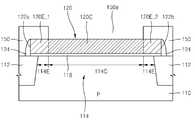
상기 게이트 전극(120)은 소정의 길이(GL) 및 폭(GW)을 가지도록 형성될 수 있다. 상기 게이트 전극(120)은 그 길이(GL) 방향에 수직인 방향, 즉 게이트 전극(120)의 폭(GW) 방향을 따라 활성 영역(114)으로부터 소자분리 영역(112) 까지 연장되어 있다. 상기 게이트 전극(120)은 그 폭(GW) 방향에서 양 단부에 각각 제1 측벽(122a) 및 제2 측벽(122b)이 있다. 상기 제1 측벽(122a) 및 제2 측벽(122b)은 각각 소자분리 영역(112) 위에 위치된다. 또한, 상기 게이트 전극(120)은 그 길이(GL) 방향에서 양 단부에 각각 제3 측벽(122c) 및 제4 측벽(122d)이 있다. 상기 제3 측벽(122c) 및 제4 측벽(122d)은 각각 활성 영역(114) 위에 위치된다.The
상기 게이트 전극(120)은 활성 영역(114)의 센터 부분(114C)을 덮는 센터 게 이트 부분(120C)과, 상기 센터 게이트 부분(120C)을 포위하는 에지 게이트 부분(120E)을 포함한다. 상기 에지 게이트 부분(120E)은 상기 제1 측벽(122a) 및 제2 측벽(122b)에 각각 인접한 양 단부에서 활성 영역(114)의 에지 부분(114E)을 덮는 제1 에지 게이트 부분(120E_1) 및 제2 에지 게이트 부분(120E_2)을 포함한다. 도 1a 및 도 1b에는 각각 에지 게이트 부분(120E)이 상기 제1 측벽(122a) 및 제2 측벽(122b)과, 상기 제3 측벽(122c) 및 제4 측벽(122d)에 걸쳐서 링(ring) 형상으로 연장되어 상기 센터 게이트 부분(120C)을 포위하도록 형성된 예가 도시되어 있다. 그러나, 본 발명은 이에 한정되지 않는다. 예를 들면, 상기 에지 게이트 부분(120E)은 상기 제1 측벽(122a) 및 제2 측벽(122b)에 각각 인접한 양 단부에 형성된 제1 에지 게이트 부분(120E_1) 및 제2 에지 게이트 부분(120E_2) 만을 포함할 수도 있다.The
일 예에서, 상기 게이트 전극(120)의 센터 게이트 부분(120C)은 불순물로 도핑되고, 상기 에지 게이트 부분(120E)은 불순물도 도핑되지 않을 수 있다. 이 때, 상기 게이트 전극(120)의 센터 게이트 부분(120C)은 상기 소스 영역(132) 및 드레인 영역(142)의 도전형과 동일한 제1 도전형, 예를 들면 N+형의 불순물이 도핑될 수 있다.In one example, the
다른 예에서, 상기 게이트 전극(120)의 센터 게이트 부분(120C)은 소스 영역(132) 및 드레인 영역(142)의 도전형과 동일한 제1 도전형의 불순물로 도핑되고, 상기 에지 게이트 부분(120E)은 상기 제1 도전형과 반대인 제2 도전형의 불순물도 도핑될 수 있다. 그러나, 본 발명의 범위 내에서 그 역도 가능하다. 또한, 상기 에 지 게이트 부분(120E)에서, 제1 에지 게이트 부분(120E_1) 및 제2 에지 게이트 부분(120E_2)에서의 도핑 농도가 동일할 수도 있고 서로 다를 수도 있다.In another example, the
또 다른 예에서, 상기 게이트 전극(120)의 센터 게이트 부분(120C) 및 에지 게이트 부분(120E)이 각각 동일한 도전형의 불순물로 도핑될 수 있다. 여기서, 상기 센터 게이트 부분(120C)의 도핑 농도와 상기 에지 게이트 부분(120E)의 도핑 농도는 상호 다를 수 있다. 예를 들면, 상기 센터 게이트 부분(120C)은 상기 소스 영역(132) 및 드레인 영역(142)의 도전형과 동일한 제1 도전형의 불순물이 비교적 고농도로 도핑되고, 상기 에지 게이트 부분(120E)은 상기 제1 도전형의 불순물이 비교적 저농도로 도핑될 수 있다.In another example, the
또 다른 예에서, 상기 게이트 전극(120)의 센터 게이트 부분(120C)은 상기 소스 영역(132) 및 드레인 영역(142)의 도전형과 동일한 제1 도전형의 불순물로 도핑되고, 상기 제1 에지 게이트 부분(120E_1) 및 제1 에지 게이트 부분(120E_2) 중 어느 하나는 불순물로 도핑되지 않고, 상기 제1 에지 게이트 부분(120E_1) 및 제2 에지 게이트 부분(120E_2) 중 다른 하나만 상기 제1 도전형과 반대인 제2 도전형의 불순물도 도핑될 수 있다.In another example, the
도 1a, 도 1b, 및 도 1c에는 N+형 불순물로 도핑된 소스 영역(132) 및 드레인 영역(142)을 가지는 N 채널 트랜지스터가 예시되어 있다. 그러나, 본 발명은 이에 한정되는 것은 아니며, P 채널 트랜지스터에 대하여도 유사한 방식으로 적용될 수 있다.1A, 1B, and 1C illustrate an N-channel transistor having a
위에서 설명한 본 발명에 따른 반도체 소자(100)에서, 게이트 전극(120)의 제1 에지 게이트 부분(120E_1) 및 제2 에지 게이트 부분(120E_2)에는 불순물이 도핑되지 않거나 상기 게이트 전극(120)의 센터 게이트 부분(120C) 보다 낮은 농도의 불순물, 또는 센터 게이트 부분(120C)과 반대 도전형의 불순물이 도핑되어 있다. 따라서, 게이트 전극(120)의 제1 에지 게이트 부분(120E_1) 및 제2 에지 게이트 부분(120E_2)이 센터 게이트 부분(120C)과 동일한 조건으로 블순물 도핑된 경우와 비교할 때, 소자분리 영역(112)과 활성 영역(114)과의 계면에 인접한 활성 영역(114)의 에지 부분(114E) 위에 있는 제1 에지 게이트 부분(120E_1) 및 제2 에지 게이트 부분(120E_2)에서 디플리션(depletion) 효과가 발생하여, 등가산화막 두께가 증가하는 결과가 얻어지고, 게이트 전극(120)과 기판(110)과의 일함수 (work function) 전위차 (Φms)가 줄어들게 된다. 그 결과, 게이트 전극(120)의 제1 에지 게이트 부분(120E_1) 및 제2 에지 게이트 부분(120E_2) 아래의 활성 영역(114)의 에지 부분(114E)에서 한계 전압(Vth)이 커지게 되므로, 활성 영역(114)의 에지 부분(114E)에서 원하지 않는 기생 트랜지스터로 인한 험프 현상이 발생되지 않는다.In the
도 2a 및 도 2b 내지 도 4a 및 도 4b는 본 발명의 제1 실시예에 따른 반도체 소자의 제조 방법을 설명하기 위하여 공정 순서에 따라 도시한 단면도들이다. 도 2a, 도 3a, 및 도 4a는 도 1a의 Ib - Ib' 단면에 대응되는 부분의 단면도들이고, 도 2b, 도 3b, 및 도 4b는 도 1a의 Ic - Ic' 단면에 대응되는 부분의 단면도들이다. 도 2a 및 도 2b 내지 도 4a 및 도 4b에 있어서, 도 1a, 도 1b, 및 도 1c에서와 동일한 참조 부호는 동일한 구성 요소를 의미하여, 여기서는 중복을 피하기 위하여 이들에 대한 상세한 설명은 생략한다.FIGS. 2A and 2B to FIGS. 4A and 4B are cross-sectional views illustrating a method of fabricating a semiconductor device according to a first embodiment of the present invention. Figs. 2A, 3A and 4A are sectional views of a portion corresponding to the section Ib-Ib 'of Fig. 1A, and Figs. 2B, 3B and 4B are sectional views of a portion corresponding to a section Ic- admit. In Figs. 2A and 2B to Figs. 4A and 4B, the same reference numerals as in Figs. 1A, 1B, and 1C denote the same elements, and a detailed description thereof will be omitted here to avoid redundancy.
도 2a 및 도 2b를 참조하면, 소정의 도전형의 웰(well)이 형성된 기판(110), 예를 들면 실리콘 기판에 소자분리 영역(112)을 형성하여 활성 영역(114)을 정의한다. 예를 들면, 상기 활성 영역(114)에 N 채널 트랜지스터를 형성하는 경우에는 상기 웰은 P 웰로 이루어지고, P 채널 트랜지스터를 형성하는 경우에는 상기 웰은 N 웰로 이루어질 수 있다. 본 예에서는 N 채널 트랜지스터를 형성하는 경우를 예로 들어 설명한다.2A and 2B, an
그 후, 상기 활성 영역(114)의 일부 영역에 저농도 불순물을 주입하여 N-형의 소스 드리프트 영역(130) 및 드레인 드리프트 영역(140)을 형성한다. 예를 들면, 상기 소스 드리프트 영역(130) 및 드레인 드리프트 영역(140)을 형성하기 위하여, 약 5×10¹¹ ∼ 5×10¹³ atoms/㎠의 도즈량으로 P 도핑을 행할 수 있다.Thereafter, a low concentration impurity is implanted into a part of the
그 후, 상기 기판(110)의 활성 영역(114) 위에 게이트 절연막(118) 및 도핑되지 않은 폴리실리콘층으로 이루어지는 게이트 패턴(120P)을 형성하고, 상기 게이트 패턴(120P)의 측벽에 절연 스페이서(124)를 형성한다. 상기 게이트 패턴(120P)의 폭(GW) 방향에서 양 단부에 있는 제1 측벽(122a) 및 제2 측벽(122b)은 소자분리 영역(112) 위에 위치되도록 상기 폭(GW) 방향에서 활성 영역(114) 및 소자분리 영역(112)에 걸쳐서 연장되어 있다. 따라서, 상기 게이트 패턴(120P)의 폭(GW) 방향에서 양 단부는 소자분리 영역(112)과 활성 영역(114)과의 계면 위를 덮게 된다. 상기 게이트 패턴(120P)의 길이(GL) 방향에서 양 단부에 있는 제3 측벽(122c) 및 제4 측벽(122d)은 활성 영역(114) 위에 위치된다.Thereafter, a
도 3a 및 도 3b를 참조하면, 상기 게이트 패턴(120P) 중 상기 활성 영역(114)의 센터 부분(114C)을 덮고 있는 중앙부를 노출시키는 제1 개구(150a)와, 상기 소스 드리프트 영역(130) 및 드레인 드리프트 영역(140)의 일부 영역들을 노출시키는 복수의 제2 개구(150b)를 포함하는 마스크 패턴(150)을 상기 게이트 패턴(120P) 및 기판(110) 위에 형성한다. 예를 들면, 상기 마스크 패턴(150)은 포토레지스트 패턴으로 이루어질 수 있다.3A and 3B, a
도 4a 및 도 4b를 참조하면, 상기 마스크 패턴(150)에 형성된 제1 개구(150a)와 복수의 제2 개구(150b)를 통해 상기 게이트 패턴(120P) 및 활성 영역(114)에 제1 도전형의 고농도 불순물, 예를 들면 N+ 형의 불순물을 주입하여 N+ 형의 소스 영역(132) 및 드레인 영역(142)을 형성하는 동시에, 상기 게이트 패턴(120P)의 중앙부에 제1 도전형의 불순물로 도핑된 센터 게이트 부분(120C)을 형성한다. 그 결과, 불순물로 도핑된 센터 게이트 부분(120C)과 불순물로 도핑되지 않은 에지 게이트 부분(120E)을 포함하는 게이트 전극(120)이 형성된다. 예를 들면, 상기 N+ 형의 소스 영역(132) 및 드레인 영역(142)과 센터 게이트 부분(120C)을 형성하기 위하여, 약 1×10¹⁵ ∼ 2×10¹⁶ atoms/㎠의 도즈량으로 P 도핑을 행할 수 있다.Referring to FIGS. 4A and 4B, the
그 후, 상기 마스크 패턴(150)을 제거하고, 도 1b 및 도 1c에 예시된 바와 같이, 상기 게이트 전극(120) 및 기판(110) 위에 상기 층간절연막(160)을 형성한 후, 상기 층간절연막(160)의 일부를 제거하여 상기 소스 영역(132) 및 드레인 영역(142)을 노출시키는 복수의 콘택홀을 형성하고, 상기 콘택홀 내에 상기 소스 영역(132) 및 드레인 영역(142)에 각각 전기적으로 연결되는 콘택 플러그(170)를 형성한다.Thereafter, the
그 후, 도시하지는 않았으나, 상기 층간절연막(160) 위에 상기 콘택 플러그(170)에 전기적으로 연결되는 배선용 도전층을 형성할 수 있다.Thereafter, although not shown, a wiring conductive layer electrically connected to the
도 5a 및 도 5b는 본 발명의 제2 실시예에 따른 반도체 소자의 제조 방법을 설명하기 위하여 도시한 단면도들이다. 도 5a는 도 1a의 Ib - Ib' 단면에 대응되는 부분의 단면도이고, 도 5b는 도 1a의 Ic - Ic' 단면에 대응되는 부분의 단면도이다. 도 5a 및 도 5b에 있어서, 도 1a, 도 1b, 및 도 1c, 그리고 도 2a 및 도 2b 내지 도 4a 및 도 4b에서와 동일한 참조 부호는 동일한 구성 요소를 의미하여, 여기서는 중복을 피하기 위하여 이들에 대한 상세한 설명은 생략한다.5A and 5B are cross-sectional views illustrating a method of manufacturing a semiconductor device according to a second embodiment of the present invention. FIG. 5A is a cross-sectional view of a portion corresponding to the section Ib-Ib 'of FIG. 1A, and FIG. 5B is a cross-sectional view of a portion corresponding to a section of the IC-IC' of FIG. In FIGS. 5A and 5B, the same reference numerals as in FIGS. 1A, 1B and 1C and FIGS. 2A and 2B to 4A and 4B denote the same elements. Here, in order to avoid redundancy, A detailed description thereof will be omitted.
도 5a 및 도 5b를 참조하면, 도 2a 및 도 2b 내지 도 4a 및 도 4b를 참조하여 설명한 본 발명의 제1 실시예에 따른 반도체 소자의 제조 방법에 따라 기판(110)상에 불순물로 도핑된 센터 게이트 부분(120C)과 불순물로 도핑되지 않은 에지 게이트 부분(120E)을 포함하는 게이트 전극(120)을 형성한 후, 상기 게이트 전극(120) 중 제1 에지 게이트 부분(120E_1) 및 제2 에지 게이트 부분(120E_2) 만을 노출시키는 개구(250a, 250b)가 형성된 마스크 패턴(250)을 상기 게이트 전극(120) 및 기판(110) 위에 형성한다. 예를 들면, 상기 마스크 패턴(250)은 포토레지스트 패턴으로 이루어질 수 있다.Referring to FIGS. 5A and 5B, a method of manufacturing a semiconductor device according to a first embodiment of the present invention, which has been described with reference to FIGS. 2A and 2B to 4A and 4B, After forming the
그 후, 상기 마스크 패턴(250)에 형성된 개구(250a, 250b)를 통해 상기 게이트 전극(120)의 제1 에지 게이트 부분(120E_1) 및 제2 에지 게이트 부분(120E_2)에 상기 제1 도전형과는 반대인 제2 도전형의 불순물, 예를 들면 P 형 또는 P+형의 불순물을 도핑하여, 제2 도전형의 불순물로 도핑된 제1 에지 게이트 부분(220E_1) 및 제2 에지 게이트 부분(220E_2)을 형성한다. 그 결과, 제1 도전형의 불순물로 도핑된 센터 게이트 부분(120C)과, 제2 도전형의 불순물로 도핑된 제1 에지 게이트 부분(220E_1) 및 제2 에지 게이트 부분(220E_2)을 포함하는 게이트 전극(220)이 형성된다.The first conductive type and the second conductive type are then applied to the first edge gate portion 120E_1 and the second edge gate portion 120E_2 of the
상기 불순물로 도핑된 제1 에지 게이트 부분(220E_1) 및 제2 에지 게이트 부분(220E_2)을 형성하기 위한 이온 주입 공정은 상기 기판(110)의 다른 영역, 예를 들면 PMOS 트랜지스터 영역(도시 생략)에 P 채널 트랜지스터의 소스 영역 및 드레인 영역을 형성하기 위한 이온 주입 공정시 사용되는 마스크 패턴과 동일한 마스크 패턴을 사용하여 그와 동시에 행해질 수 있다.The ion implantation process for forming the first edge gate portion 220E_1 and the second edge gate portion 220E_2 doped with the impurity may be performed in another region of the
필요에 따라, 도 5a 및 도 5b를 참조하여 설명한 제2 도전형의 불순물로 도핑된 제1 에지 게이트 부분(220E_1) 및 제2 에지 게이트 부분(220E_2) 형성 공정을 도 4a 및 도 4b를 참조하여 설명한 제1 도전형의 불순물로 도핑된 센터 게이트 부분(120C) 형성 공정 전에 행할 수도 있다.If necessary, the process of forming the first edge gate portion 220E_1 and the second edge gate portion 220E_2 doped with the impurity of the second conductivity type described with reference to FIGS. 5A and 5B will be described with reference to FIGS. 4A and 4B Or may be performed before the step of forming the
상기 제2 도전형의 불순물로 도핑된 제1 에지 게이트 부분(220E_1) 및 제2 에지 게이트 부분(220E_2)이 각각 동일한 도핑 농도를 가질 수도 있고 서로 다른 도핑 농도를 가질 수도 있다. 상기 제2 도전형의 불순물로 도핑된 제1 에지 게이트 부분(220E_1) 및 제2 에지 게이트 부분(220E_2)이 서로 다른 도핑 농도를 가지는 구조를 형성하기 위하여, 도 5a 및 도 5b에서의 이온 주입 공정시, 상기 마스크 패턴(250) 대신, 상기 제1 에지 게이트 부분(120E_1) 및 제2 에지 게이트 부분(120E_2) 중 어느 하나의 부분 만을 노출시키는 마스크 패턴을 이용한 1차 이온 주입 공정을 행한 후, 다시 상기 제1 에지 게이트 부분(120E_1) 및 제2 에지 게이트 부분(120E_2) 중 다른 하나의 부분 만을 노출시키는 마스크 패턴을 이용한 2차 이온 주입 공정을 행할 수 있다. 여기서, 상기 1차 이온 주입 공정 및 2차 이온 주입 공정시의 도즈량을 다르게 설정할 수 있다.The first edge gate portion 220E_1 and the second edge gate portion 220E_2 doped with the impurity of the second conductivity type may have the same doping concentration or different doping concentrations, respectively. In order to form a structure in which the first edge gate portion 220E_1 and the second edge gate portion 220E_2 doped with the impurity of the second conductivity type have different doping densities, the ion implantation process in FIGS. 5A and 5B A first ion implantation process using a mask pattern that exposes only one of the first edge gate portion 120E_1 and the second edge gate portion 120E_2 is performed in place of the
또한, 도시하지는 않았으나, 도 5a 및 도 5b에서 상기 마스크 패턴(250) 대신, 상기 제1 에지 게이트 부분(120E_1) 및 제2 에지 게이트 부분(120E_2) 중 어느 하나의 부분 만을 노출시키는 개구가 형성된 마스크 패턴(도시 생략)을 형성하여 상기 제1 에지 게이트 부분(120E_1) 및 제2 에지 게이트 부분(120E_2) 중 어느 하나의 부분에만 제2 도전형, 예들 들면 P 형 또는 P+형의 불순물을 도핑하고, 상기 제1 에지 게이트 부분(120E_1) 및 제2 에지 게이트 부분(120E_2) 중 다른 하나의 부분에는 불순물을 도핑하지 않는 공정을 행할 수도 있다.5A and 5B, instead of the
또는, 도시하지는 않았으나, 상기 마스크 패턴(250)의 개구(250a, 250b)를 통해 상기 센터 게이트 부분(120C)의 불순물 농도 보다 더 낮은 농도의 제1 도전형의 불순물을 주입하여 상기 제1 에지 게이트 부분(120E_1) 및 제2 에지 게이트 부분(120E_2)에 각각 낮은 농도의 불순물, 예를 들면 N- 형의 불순물을 주입할 수도 있다.Alternatively, impurities of the first conductivity type may be implanted through the
그 후, 도 4a 및 도 4b를 참조하여 설명한 바와 유사한 방법으로 게이트 전극(120) 및 기판(110) 위에 층간절연막(160) 및 콘택 플러그(170)를 형성한다.Thereafter, an
도 6 내지 도 9는 본 발명에 따른 반도체 소자의 트랜지스터 및 비교예에 따른 반도체 소자의 트랜지스터에서의 전기적 특성들을 비교한 그래프들이다.FIGS. 6 to 9 are graphs comparing electrical characteristics of the transistors of the semiconductor device according to the present invention and the transistors of the semiconductor device according to the comparative example.
도 6 내지 도 9의 평가를 위하여, 본 발명에 따른 반도체 소자로서 게이트 전극의 에지 게이트 부분에는 불순물을 도핑하지 않고 게이트 전극의 센터 게이트 부분만 N+ 형 불순물로 도핑하여 고전압 트랜지스터용 N 채널 트랜지스터를 제조하였다. 비교예로서, 게이트 전극의 에지 게이트 부분이 센터 게이트 부분과 동일한 조건으로 N+ 형 블순물로 도핑된 것을 제외하고 본 발명의 경우와 동일한 조건으로 고전압 트랜지스터용 N 채널 트랜지스터를 제조하였다.For the evaluation of FIGS. 6 to 9, as the semiconductor device according to the present invention, only the center gate portion of the gate electrode is doped with an N + type impurity without doping the edge gate portion of the gate electrode with an impurity to manufacture an N channel transistor for a high voltage transistor Respectively. As a comparative example, an N-channel transistor for a high-voltage transistor was manufactured under the same conditions as in the case of the present invention, except that the edge gate portion of the gate electrode was doped with an N + type compound in the same condition as the center gate portion.
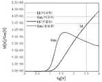
도 6은 본 발명에 따른 반도체 소자의 트랜지스터 및 비교예에 따른 반도체 소자의 트랜지스터에서의 트랜스컨덕턴스(Gm) 특성과, Vd - Vg 특성을 비교한 그래프이다 (Vd = 0.1 V).6 is a graph (Vd = 0.1 V) comparing the transconductance (Gm) characteristic and the Vd-Vg characteristic in the transistor of the semiconductor device according to the present invention and the transistor of the semiconductor device according to the comparative example.
도 6에서, 본 발명에 따른 반도체 소자에서 게이트 전극 중 활성 영역의 센터 부분 위에 있는 센터 게이트 부분에만 트랜지스터 채널의 도전 타입과 동일한 도전형의 도판트를 포함하는 경우에도, 비교예의 경우와 대략 일치하는 트랜스컨덕턴스 (Gm) 특성 및 Vd - Vg 특성이 얻어지는 것을 확인할 수 있다. 도 6에 나타난 Gm - Vg 플롯을 이용하여 Vth를 정의할 때, 본 발명에서와 같이 게이트 전극 중 활성 영역의 중심 영역에 대응하는 부분에만 트랜지스터 채널의 도전 타입과 동일한 도전형의 도판트를 포함하여도 트랜지스터의 Vth 특성에 악영향을 미치지 않음을 알 수 있다.In Fig. 6, even in the semiconductor device according to the present invention, only the center gate portion on the center portion of the active region of the gate electrode includes the dopant of the same conductivity type as the conduction type of the transistor channel, The transconductance (Gm) characteristic and the Vd - Vg characteristic can be obtained. When Vth is defined using the Gm-Vg plot shown in FIG. 6, only a portion of the gate electrode corresponding to the central region of the active region, as in the present invention, includes a dopant of the same conductivity type as that of the transistor channel The Vth characteristic of the transistor is not adversely affected.
도 7은 본 발명에 따른 반도체 소자의 트랜지스터 및 비교예에 따른 반도체 소자의 트랜지스터에서의 Id - Vd 특성을 비교한 그래프이다 (Vg = 30 V).FIG. 7 is a graph comparing the Id-Vd characteristics (Vg = 30 V) in the transistor of the semiconductor device according to the present invention and the transistor of the semiconductor device according to the comparative example.
본 발명에 따른 반도체 소자에서 게이트 전극 중 활성 영역의 센터 부분 위에 있는 센터 게이트 부분에만 트랜지스터 채널의 도전 타입과 동일한 도전형의 도판트를 포함하는 경우에도, 비교예의 경우와 동일한 포화 전류 (saturation current) 특성이 얻어지는 것을 알 수 있다.Even when the semiconductor device according to the present invention includes a dopant of the same conduction type as the conduction type of the transistor channel only in the center gate portion above the center portion of the active region of the gate electrode in the semiconductor device according to the present invention, Characteristics can be obtained.
도 8은 본 발명에 따른 반도체 소자의 트랜지스터 및 비교예에 따른 반도체 소자의 트랜지스터에서 Vg = 0 V일 때의 Ioff (off-current) 특성을 평가하기 위하여 Id - Vd 특성을 비교한 그래프이다.8 is a graph comparing Id-Vd characteristics for evaluating Ioff (off-current) characteristics when Vg = 0 V in the transistors of the semiconductor device according to the present invention and the transistors of the semiconductor device according to the comparative example.
도 9는 본 발명에 따른 반도체 소자의 트랜지스터 및 비교예에 따른 반도체 소자의 트랜지스터에서 Vd = 0.1 V인 조건 하에서 Vb (back bias voltage)를 각각 0 V, -2 V, 및 -4 V로 할 때의 Id - Vg 특성을 비교한 그래프이다.9 is a graph showing the relationship between the Vb (back bias voltage) at 0 V, -2 V, and -4 V under the condition of Vd = 0.1 V in the transistor of the semiconductor device according to the present invention and the transistor of the semiconductor device according to the comparative example And the Id - Vg characteristics of the second embodiment.
도 8 및 도 9로부터, 본 발명에 따른 반도체 소자의 트랜지스터에서 비교예의 경우에 비해 Ioff 가 감소되었으며, 험프 현상이 개선된 것을 알 수 있다.8 and 9, it can be seen that Ioff is reduced and the hump phenomenon is improved in the transistor of the semiconductor device according to the present invention, as compared with the comparative example.
도 1a는 본 발명의 바람직한 실시예에 따른 반도체 소자의 요부 구성을 도시한 레이아웃이다.BRIEF DESCRIPTION OF THE DRAWINGS FIG. 1A is a layout showing a configuration of a semiconductor device according to a preferred embodiment of the present invention. FIG.
도 1b는 도 1a의 Ib - Ib'선 단면도이다.1B is a cross-sectional view taken along line Ib-Ib 'of FIG. 1A.
도 1c는 도 1a의 Ic - Ic'선 단면도이다.1C is a sectional view taken along the line Ic - Ic 'of FIG. 1A.
도 2a 및 도 2b 내지 도 4a 및 도 4b는 본 발명의 제1 실시예에 따른 반도체 소자의 제조 방법을 설명하기 위하여 공정 순서에 따라 도시한 단면도들이다.FIGS. 2A and 2B to FIGS. 4A and 4B are cross-sectional views illustrating a method of fabricating a semiconductor device according to a first embodiment of the present invention.
도 5a 및 도 5b는 본 발명의 제2 실시예에 따른 반도체 소자의 제조 방법을 설명하기 위하여 도시한 단면도들이다.5A and 5B are cross-sectional views illustrating a method of manufacturing a semiconductor device according to a second embodiment of the present invention.
도 6은 본 발명에 따른 반도체 소자의 트랜지스터 및 비교예에 따른 반도체 소자의 트랜지스터에서의 트랜스컨덕턴스(Gm) 특성과 Vd - Vg 특성을 비교한 그래프이다.FIG. 6 is a graph comparing transconductance (Gm) characteristics and Vd - Vg characteristics in the transistors of the semiconductor device according to the present invention and the transistor of the semiconductor device according to the comparative example.
도 7은 본 발명에 따른 반도체 소자의 트랜지스터 및 비교예에 따른 반도체 소자의 트랜지스터에서의 Id - Vd 특성을 비교한 그래프이다.7 is a graph comparing Id-Vd characteristics in the transistors of the semiconductor device according to the present invention and the transistors of the semiconductor device according to the comparative example.
도 8은 본 발명에 따른 반도체 소자의 트랜지스터 및 비교예에 따른 반도체 소자의 트랜지스터에서 Vg = 0 V일 때의 Ioff (off-current) 특성을 평가하기 위하여 Id - Vd 특성을 비교한 그래프이다.8 is a graph comparing Id-Vd characteristics for evaluating Ioff (off-current) characteristics when Vg = 0 V in the transistors of the semiconductor device according to the present invention and the transistors of the semiconductor device according to the comparative example.
도 9는 본 발명에 따른 반도체 소자의 트랜지스터 및 비교예에 따른 반도체 소자의 트랜지스터에서 Id - Vg 특성을 비교한 그래프이다.9 is a graph comparing Id-Vg characteristics in the transistors of the semiconductor device according to the present invention and the transistors of the semiconductor device according to the comparative example.
<도면의 주요 부분에 대한 부호의 설명>Description of the Related Art
100: 반도체 소자, 110: 기판, 112: 소자분리 영역, 114: 활성 영역, 114C: 센터 부분, 114E: 에지 부분, 120: 게이트 전극, 120C: 센터 게이트 부분, 120E: 에지 게이트 부분, 120E_1: 제1 에지 게이트 부분, 120E_2: 제2 에지 게이트 부분, 120P: 게이트 패턴, 122a: 제1 측벽, 122b: 제2 측벽, 122c: 제3 측벽, 122d: 제4 측벽, 124: 절연 스페이서, 130: 소스 드리프트 영역, 132: 소스 영역, 140: 드레인 드리프트 영역, 142: 드레인 영역, 150: 마스크 패턴, 160: 층간절연막, 170: 콘택 플러그, 220: 게이트 전극, 220E_1: 제1 에지 게이트 부분, 220E_2: 제2 에지 게이트 부분, 250: 마스크 패턴.The semiconductor device according to
Claims (30)
Translated fromKoreanPriority Applications (5)
| Application Number | Priority Date | Filing Date | Title |
|---|---|---|---|
| KR1020080049674AKR101413651B1 (en) | 2008-05-28 | 2008-05-28 | Semiconductor device having transistor and method for manufacturing the same |
| US12/268,031US20090294848A1 (en) | 2008-05-28 | 2008-11-10 | Semiconductor device having transistor and method of manufacturing the same |
| TW098111697ATW200950086A (en) | 2008-05-28 | 2009-04-08 | Semiconductor device having transistor and method of manufacturing the same |
| JP2009126207AJP2009290211A (en) | 2008-05-28 | 2009-05-26 | Semiconductor device and method of manufacturing the same |
| US12/712,260US8247286B2 (en) | 2008-05-28 | 2010-02-25 | Semiconductor device having transistor and method of manufacturing the same |
Applications Claiming Priority (1)
| Application Number | Priority Date | Filing Date | Title |
|---|---|---|---|
| KR1020080049674AKR101413651B1 (en) | 2008-05-28 | 2008-05-28 | Semiconductor device having transistor and method for manufacturing the same |
Publications (2)
| Publication Number | Publication Date |
|---|---|
| KR20090123537A KR20090123537A (en) | 2009-12-02 |
| KR101413651B1true KR101413651B1 (en) | 2014-07-01 |
Family
ID=41378701
Family Applications (1)
| Application Number | Title | Priority Date | Filing Date |
|---|---|---|---|
| KR1020080049674AActiveKR101413651B1 (en) | 2008-05-28 | 2008-05-28 | Semiconductor device having transistor and method for manufacturing the same |
Country Status (4)
| Country | Link |
|---|---|
| US (2) | US20090294848A1 (en) |
| JP (1) | JP2009290211A (en) |
| KR (1) | KR101413651B1 (en) |
| TW (1) | TW200950086A (en) |
Families Citing this family (19)
| Publication number | Priority date | Publication date | Assignee | Title |
|---|---|---|---|---|
| US8138051B2 (en)* | 2009-06-19 | 2012-03-20 | Globalfoundries Singapore Pte. Ltd. | Integrated circuit system with high voltage transistor and method of manufacture thereof |
| TWI394278B (en)* | 2009-12-29 | 2013-04-21 | Vanguard Int Semiconduct Corp | Semiconductor structure and fabrication method thereof |
| US9123807B2 (en)* | 2010-12-28 | 2015-09-01 | Broadcom Corporation | Reduction of parasitic capacitance in a semiconductor device |
| JP2012191088A (en)* | 2011-03-13 | 2012-10-04 | Seiko Instruments Inc | Semiconductor device and reference voltage generating circuit |
| FR2981503A1 (en)* | 2011-10-13 | 2013-04-19 | St Microelectronics Rousset | TRANSISTOR MOS NOT SUBJECT TO HUMP EFFECT |
| JP6334370B2 (en)* | 2014-11-13 | 2018-05-30 | ルネサスエレクトロニクス株式会社 | Semiconductor device and manufacturing method thereof |
| CN105990115A (en)* | 2015-02-02 | 2016-10-05 | 无锡华润上华半导体有限公司 | Semiconductor device and manufacturing method thereof, and electronic device |
| US9406771B1 (en)* | 2015-09-15 | 2016-08-02 | United Microelectronics Corp. | Semiconductor structure and manufacturing method thereof |
| TWI571938B (en)* | 2015-10-15 | 2017-02-21 | 力晶科技股份有限公司 | Semiconductor component and method of manufacturing same |
| KR20180052171A (en)* | 2016-11-09 | 2018-05-18 | 삼성전자주식회사 | Design method of semiconductor integrated circuit layout and method for forming semiconductor device using the same |
| CN108039365B (en)* | 2017-09-25 | 2021-01-12 | 中国科学院微电子研究所 | Transistor, clamping circuit and integrated circuit |
| CN108039362B (en)* | 2017-09-25 | 2021-01-12 | 中国科学院微电子研究所 | Transistor, clamping circuit and integrated circuit |
| US10468494B2 (en)* | 2018-02-09 | 2019-11-05 | United Microelectronics Corp. | High-voltage device and method for fabricating the same |
| CN111092112B (en)* | 2018-10-23 | 2020-11-13 | 合肥晶合集成电路有限公司 | MOS field effect transistor and method of making the same |
| CN111048524A (en)* | 2019-11-26 | 2020-04-21 | 深圳市华星光电半导体显示技术有限公司 | Array substrate and preparation method thereof, and display panel |
| US11444169B2 (en) | 2020-02-27 | 2022-09-13 | Taiwan Semiconductor Manufacturing Company, Ltd. | Transistor device with a gate structure having recesses overlying an interface between isolation and device regions |
| CN113314610B (en) | 2020-02-27 | 2024-04-30 | 台湾积体电路制造股份有限公司 | Transistor device and method for manufacturing the same |
| JP2021192416A (en)* | 2020-06-05 | 2021-12-16 | ラピスセミコンダクタ株式会社 | Semiconductor device |
| WO2023189505A1 (en)* | 2022-03-31 | 2023-10-05 | ローム株式会社 | Semiconductor device |
Citations (3)
| Publication number | Priority date | Publication date | Assignee | Title |
|---|---|---|---|---|
| KR20000022709A (en)* | 1998-09-18 | 2000-04-25 | 포만 제프리 엘 | Depleted poly-silicon edged mosfet structure and method |
| KR20010076661A (en)* | 2000-01-27 | 2001-08-16 | 박종섭 | Semiconductor device and method for fabricating thereof |
| JP2007080956A (en) | 2005-09-12 | 2007-03-29 | Seiko Epson Corp | Semiconductor device and manufacturing method of semiconductor device |
Family Cites Families (15)
| Publication number | Priority date | Publication date | Assignee | Title |
|---|---|---|---|---|
| US5028556A (en)* | 1990-02-16 | 1991-07-02 | Hughes Aircraft Company | Process for fabricating radiation hard high voltage devices |
| JPH0496275A (en)* | 1990-08-03 | 1992-03-27 | Nkk Corp | MOS type semiconductor device |
| JPH06275821A (en)* | 1993-03-18 | 1994-09-30 | Seiko Instr Inc | Mos transistor and its manufacture |
| US5650654A (en)* | 1994-12-30 | 1997-07-22 | International Business Machines Corporation | MOSFET device having controlled parasitic isolation threshold voltage |
| JP2904081B2 (en)* | 1995-11-24 | 1999-06-14 | 日本電気株式会社 | Method for manufacturing semiconductor device |
| EP0798785B1 (en)* | 1996-03-29 | 2003-12-03 | STMicroelectronics S.r.l. | High-voltage-resistant MOS transistor, and corresponding manufacturing process |
| US5804496A (en)* | 1997-01-08 | 1998-09-08 | Advanced Micro Devices | Semiconductor device having reduced overlap capacitance and method of manufacture thereof |
| JP2001156290A (en)* | 1999-11-30 | 2001-06-08 | Nec Corp | Semiconductor device |
| US6555446B1 (en)* | 1999-12-10 | 2003-04-29 | Texas Instruments Incorporated | Body contact silicon-on-insulator transistor and method |
| JP2004253765A (en)* | 2002-12-25 | 2004-09-09 | Fuji Electric Holdings Co Ltd | Semiconductor device, method of manufacturing the same, and power converter using the same |
| JP2004281843A (en)* | 2003-03-18 | 2004-10-07 | Toshiba Corp | Electrostatic discharge protection element and semiconductor integrated circuit device having the same |
| KR100645193B1 (en)* | 2004-03-17 | 2006-11-10 | 매그나칩 반도체 유한회사 | Electrostatic discharge protection device and its manufacturing method |
| KR100587605B1 (en) | 2004-04-28 | 2006-06-08 | 매그나칩 반도체 유한회사 | High voltage transistors and manufacturing method thereof |
| KR20060098191A (en) | 2005-03-10 | 2006-09-18 | 삼성전자주식회사 | Method for manufacturing high voltage transistors. |
| US7485925B2 (en)* | 2005-08-30 | 2009-02-03 | United Microelectronics Corp. | High voltage metal oxide semiconductor transistor and fabricating method thereof |
- 2008
- 2008-05-28KRKR1020080049674Apatent/KR101413651B1/enactiveActive
- 2008-11-10USUS12/268,031patent/US20090294848A1/ennot_activeAbandoned
- 2009
- 2009-04-08TWTW098111697Apatent/TW200950086A/enunknown
- 2009-05-26JPJP2009126207Apatent/JP2009290211A/enactivePending
- 2010
- 2010-02-25USUS12/712,260patent/US8247286B2/enactiveActive
Patent Citations (3)
| Publication number | Priority date | Publication date | Assignee | Title |
|---|---|---|---|---|
| KR20000022709A (en)* | 1998-09-18 | 2000-04-25 | 포만 제프리 엘 | Depleted poly-silicon edged mosfet structure and method |
| KR20010076661A (en)* | 2000-01-27 | 2001-08-16 | 박종섭 | Semiconductor device and method for fabricating thereof |
| JP2007080956A (en) | 2005-09-12 | 2007-03-29 | Seiko Epson Corp | Semiconductor device and manufacturing method of semiconductor device |
Also Published As
| Publication number | Publication date |
|---|---|
| US8247286B2 (en) | 2012-08-21 |
| TW200950086A (en) | 2009-12-01 |
| US20090294848A1 (en) | 2009-12-03 |
| KR20090123537A (en) | 2009-12-02 |
| JP2009290211A (en) | 2009-12-10 |
| US20100148252A1 (en) | 2010-06-17 |
Similar Documents
| Publication | Publication Date | Title |
|---|---|---|
| KR101413651B1 (en) | Semiconductor device having transistor and method for manufacturing the same | |
| US4843023A (en) | Process for forming lightly-doped-drain (LDD) without extra masking steps | |
| US7981783B2 (en) | Semiconductor device and method for fabricating the same | |
| US20170062608A1 (en) | Semiconductor device and method of manufacturing semiconductor device | |
| JP2006049628A (en) | Semiconductor device and manufacturing method thereof | |
| US8878310B2 (en) | Flatband shift for improved transistor performance | |
| KR20180110703A (en) | Semiconductor Device Structure having Low Rdson and Manufacturing Method thereof | |
| US20060208300A1 (en) | Finfet-type semiconductor device and method for fabricating the same | |
| KR100690924B1 (en) | Semiconductor integrated circuit device and its manufacturing method | |
| KR20020065839A (en) | Method of fabricating semiconductor device | |
| KR100391959B1 (en) | Semiconductor apparatus and method of manufacture | |
| US20050116265A1 (en) | Semiconductor device | |
| US7994584B2 (en) | Semiconductor device having non-silicide region in which no silicide is formed on diffusion layer | |
| US6667524B1 (en) | Semiconductor device with a plurality of semiconductor elements | |
| JPH11163321A (en) | Semiconductor device and manufacturing method thereof | |
| US7247909B2 (en) | Method for forming an integrated circuit with high voltage and low voltage devices | |
| KR100331844B1 (en) | Complementary metal oxide semiconductor device | |
| US6472712B1 (en) | Semiconductor device with reduced transistor leakage current | |
| KR100223483B1 (en) | Soi mos transistor device and method of manufacturing the same | |
| KR100587605B1 (en) | High voltage transistors and manufacturing method thereof | |
| KR100424414B1 (en) | Method for forming high voltage transistor | |
| US7547592B2 (en) | PMOS depletable drain extension made from NMOS dual depletable drain extensions | |
| US20070090454A1 (en) | Transistor device | |
| JPH06216380A (en) | Semiconductor device and manufacture thereof | |
| US8110468B2 (en) | DMOS-transistor having improved dielectric strength of drain and source voltages |
Legal Events
| Date | Code | Title | Description |
|---|---|---|---|
| PA0109 | Patent application | Patent event code:PA01091R01D Comment text:Patent Application Patent event date:20080528 | |
| PG1501 | Laying open of application | ||
| A201 | Request for examination | ||
| PA0201 | Request for examination | Patent event code:PA02012R01D Patent event date:20130503 Comment text:Request for Examination of Application Patent event code:PA02011R01I Patent event date:20080528 Comment text:Patent Application | |
| E902 | Notification of reason for refusal | ||
| PE0902 | Notice of grounds for rejection | Comment text:Notification of reason for refusal Patent event date:20140129 Patent event code:PE09021S01D | |
| E701 | Decision to grant or registration of patent right | ||
| PE0701 | Decision of registration | Patent event code:PE07011S01D Comment text:Decision to Grant Registration Patent event date:20140617 | |
| GRNT | Written decision to grant | ||
| PR0701 | Registration of establishment | Comment text:Registration of Establishment Patent event date:20140624 Patent event code:PR07011E01D | |
| PR1002 | Payment of registration fee | Payment date:20140625 End annual number:3 Start annual number:1 | |
| PG1601 | Publication of registration | ||
| FPAY | Annual fee payment | Payment date:20190530 Year of fee payment:6 | |
| PR1001 | Payment of annual fee | Payment date:20190530 Start annual number:6 End annual number:6 | |
| PR1001 | Payment of annual fee | Payment date:20200529 Start annual number:7 End annual number:7 | |
| PR1001 | Payment of annual fee | Payment date:20230524 Start annual number:10 End annual number:10 | |
| PR1001 | Payment of annual fee | Payment date:20240527 Start annual number:11 End annual number:11 |