KR101410926B1 - Thin film transistor and manufacturing method thereof - Google Patents
Thin film transistor and manufacturing method thereofDownload PDFInfo
- Publication number
- KR101410926B1 KR101410926B1KR1020070016778AKR20070016778AKR101410926B1KR 101410926 B1KR101410926 B1KR 101410926B1KR 1020070016778 AKR1020070016778 AKR 1020070016778AKR 20070016778 AKR20070016778 AKR 20070016778AKR 101410926 B1KR101410926 B1KR 101410926B1
- Authority
- KR
- South Korea
- Prior art keywords
- layer
- channel layer
- forming
- oxide semiconductor
- protective
- Prior art date
- Legal status (The legal status is an assumption and is not a legal conclusion. Google has not performed a legal analysis and makes no representation as to the accuracy of the status listed.)
- Active
Links
Images


Classifications
- H—ELECTRICITY
- H10—SEMICONDUCTOR DEVICES; ELECTRIC SOLID-STATE DEVICES NOT OTHERWISE PROVIDED FOR
- H10D—INORGANIC ELECTRIC SEMICONDUCTOR DEVICES
- H10D30/00—Field-effect transistors [FET]
- H10D30/60—Insulated-gate field-effect transistors [IGFET]
- H10D30/67—Thin-film transistors [TFT]
- H10D30/674—Thin-film transistors [TFT] characterised by the active materials
- H10D30/6755—Oxide semiconductors, e.g. zinc oxide, copper aluminium oxide or cadmium stannate
- H—ELECTRICITY
- H10—SEMICONDUCTOR DEVICES; ELECTRIC SOLID-STATE DEVICES NOT OTHERWISE PROVIDED FOR
- H10D—INORGANIC ELECTRIC SEMICONDUCTOR DEVICES
- H10D30/00—Field-effect transistors [FET]
- H10D30/60—Insulated-gate field-effect transistors [IGFET]
- H10D30/67—Thin-film transistors [TFT]
- H10D30/6704—Thin-film transistors [TFT] having supplementary regions or layers in the thin films or in the insulated bulk substrates for controlling properties of the device
- H10D30/6706—Thin-film transistors [TFT] having supplementary regions or layers in the thin films or in the insulated bulk substrates for controlling properties of the device for preventing leakage current
Landscapes
- Thin Film Transistor (AREA)
- Dram (AREA)
Abstract
Translated fromKoreanDescription
Translated fromKorean도 1a 및 도 1b는 본 발명의 제1 실시예에 따른 박막 트랜지스터를 보여주는 단면도 및 사시도이다.1A and 1B are a cross-sectional view and a perspective view illustrating a thin film transistor according to a first embodiment of the present invention.
도 2a 및 도 2b는 본 발명의 제2 실시예에 따른 박막 트랜지스터를 보여주는 단면도 및 사시도이다.2A and 2B are a cross-sectional view and a perspective view illustrating a thin film transistor according to a second embodiment of the present invention.
도 3a 내지 도 3e는 본 발명의 제1 실시예에 따른 박막 트랜지스터의 제조방법을 보여주는 단면도이다.3A to 3E are cross-sectional views illustrating a method of manufacturing a thin film transistor according to a first embodiment of the present invention.
도 4a 내지 도 4f는 본 발명의 제2 실시예에 따른 박막 트랜지스터의 제조방법을 보여주는 단면도이다.4A to 4F are cross-sectional views illustrating a method of manufacturing a thin film transistor according to a second embodiment of the present invention.
도 5a 내지 도 5d는 본 발명의 제3 실시예에 따른 박막 트랜지스터의 제조방법을 보여주는 단면도이다.5A to 5D are cross-sectional views illustrating a method of manufacturing a thin film transistor according to a third embodiment of the present invention.
도 6은 본 발명의 제3 실시예에 따라 제조한 박막 트랜지스터의 전압-전류 특성을 보여주는 그래프이다.6 is a graph showing voltage-current characteristics of a thin film transistor manufactured according to a third embodiment of the present invention.
<도면의 주요 부분에 대한 부호의 설명>Description of the Related Art
10 : 감광층 패턴 100, 200 : 기판10:
110, 210 : 채널층 120, 220 : 보호층110, 210:
130 : 금속층 130a, 230a : 소오스 전극130:
130b, 230b : 드레인 전극 140, 240 : 게이트 절연층130b, 230b:
150, 250 : 게이트 전극 160, 260 : 패시베이션층150, 250:
M : 마스크M: Mask
1. 발명의 분야1. Field of the Invention
본 발명은 반도체 소자 및 그 제조방법에 관한 것으로, 보다 상세하게는 박막 트랜지스터 및 그 제조방법에 관한 것이다.The present invention relates to a semiconductor device and a method of manufacturing the same, and more particularly, to a thin film transistor and a manufacturing method thereof.
2. 관련기술의 설명2. Description of Related Technology
박막 트랜지스터(Thin film transistor)는 액정표시장치 또는 유기발광표시장치 등과 같은 평판표시장치에서 스위칭 소자로 사용된다. 박막 트랜지스터의 이동도(mobility) 또는 누설전류 등은 채널층의 재질 및 상태에 크게 좌우된다.Thin film transistors are used as switching devices in flat panel display devices such as liquid crystal display devices and organic light emitting display devices. The mobility or leakage current of the thin film transistor largely depends on the material and state of the channel layer.
현재 상용화되어 있는 액정표시장치에서, 박막 트랜지스터의 채널층은 대부분 비정질 실리콘층이다. 박막 트랜지스터의 채널층이 비정질 실리콘층일 때, 이동도는 0.5㎠/Vs 내외로 매우 낮기 때문에, 액정표시장치의 동작 속도를 증가시키기 어렵다.In the currently commercialized liquid crystal display device, the channel layer of the thin film transistor is mostly an amorphous silicon layer. When the channel layer of the thin film transistor is an amorphous silicon layer, the mobility is very low, about 0.5 cm 2 / Vs, so that it is difficult to increase the operating speed of the liquid crystal display device.
이에, 상기 비정질 실리콘층보다 이동도가 높은 산화물 반도체 물질층, 예컨대 ZnO 계열(based) 물질층을 상기 박막 트랜지스터의 채널층으로 사용하기 위한 연구가 진행되고 있다. ZnO 계열 물질층 중 하나인 Ga-In-Zn-O층의 이동도는 비정질 실리콘층의 이동도의 수십 배 이상이기 때문에, 상기 Ga-In-Zn-O층을 채널층으로 사용한 박막 트랜지스터는 차세대 표시장치의 구동 소자로서 기대를 모으고 있다.Research has been conducted to use an oxide semiconductor material layer having a higher mobility than the amorphous silicon layer, for example, a ZnO based material layer as a channel layer of the thin film transistor. Since the mobility of the Ga-In-Zn-O layer, which is one of the ZnO-based material layers, is several tens times higher than the mobility of the amorphous silicon layer, the thin film transistor using the Ga- And is expected as a driving element of a display device.
그러나 ZnO 계열 물질층을 박막 트랜지스터의 채널층으로 적용하는 경우, 채널층을 형성한 이후의 공정에서 채널층이 손상되고, 그 결과 소자의 전기적 특성이 열화되기 쉽다.However, when the ZnO-based material layer is used as a channel layer of a thin film transistor, the channel layer is damaged in a process after forming the channel layer, and as a result, the electrical characteristics of the device are likely to deteriorate.
본 발명이 이루고자 하는 기술적 과제는 상술한 종래의 문제점을 개선하기 위한 것으로서, 비정질 실리콘보다 이동도가 높고, 플라즈마에 의한 특성 열화가 억제된 채널층을 갖는 박막 트랜지스터를 제공하는데 있다.SUMMARY OF THE INVENTION The present invention provides a thin film transistor having a channel layer having higher mobility than amorphous silicon and suppressing deterioration of characteristics due to plasma.
본 발명이 이루고자 하는 다른 기술적 과제는 상기 박막 트랜지스터의 제조방법을 제공하는데 있다.According to another aspect of the present invention, there is provided a method of manufacturing the thin film transistor.
상기 기술적 과제를 달성하기 위하여, 본 발명은 산화물 반도체 물질로 형성된 채널층과, 상기 채널층 상에 서로 마주보며 위치하는 소오스 전극 및 드레인 전극과, 상기 소오스 전극 및 상기 드레인 전극의 아래에서 상기 채널층을 커버하도록 형성된 보호층과, 상기 채널층에 전계를 인가하기 위한 게이트 전극 및 상기 게이트 전극과 상기 채널층 사이에 개재된 게이트 절연층을 포함하는 것을 특징으로 하는 박막 트랜지스터를 제공한다.According to an aspect of the present invention, there is provided a semiconductor device comprising: a channel layer formed of an oxide semiconductor material; source and drain electrodes facing each other on the channel layer; A gate electrode for applying an electric field to the channel layer, and a gate insulating layer interposed between the gate electrode and the channel layer.
여기서, 상기 채널층은 ZnO 계열 물질층일 수 있다.Here, the channel layer may be a ZnO-based material layer.
상기 채널층은 a(In2O3)·b(Ga2O3)·c(ZnO)층(여기서, a, b, c는 각각 a≥0, b≥0, c>0의 조건을 만족시키는 실수)일 수 있다.Wherein the channel layer is formed of a material selected from the group consisting of a (In2 O3 ) .b (Ga2 O3 ) c (ZnO) layer (where a, b and c satisfy the conditions of a? 0, b? 0, .
상기 채널층은 a(In2O3)·b(Ga2O3)·c(ZnO)층(여기서, a, b, c는 각각 a≥1, b≥1, 0<c≤1의 조건을 만족시키는 실수)일 수 있다.Wherein the channel layer is a layer of a (In2 O3 ) b (Ga2 O3 ) c (ZnO) layer wherein a, b and c satisfy the conditions of a? 1, b? 1, ). ≪ / RTI >
상기 보호층은 상기 채널층과 상기 소오스 전극 및 상기 드레인 전극이 접촉하는 콘택 영역을 제공할 수 있다.The protective layer may provide a contact region in which the channel layer and the source electrode and the drain electrode are in contact with each other.
상기 보호층은 실리콘 산화물층 또는 실리콘 질화물층일 수 있다.The protective layer may be a silicon oxide layer or a silicon nitride layer.
상기 채널층과 상기 소오스 전극 사이 및 상기 채널층과 상기 드레인 전극 사이 각각에 오믹 콘택층이 더 형성될 수 있다.And an ohmic contact layer may be further formed between the channel layer and the source electrode and between the channel layer and the drain electrode.
상기 게이트 전극은 상기 채널층의 위에 형성될 수 있다.The gate electrode may be formed on the channel layer.
상기 게이트 전극은 상기 채널층의 아래에 형성될 수 있다.The gate electrode may be formed under the channel layer.
상기 다른 기술적 과제를 달성하기 위하여, 본 발명은 산화물 반도체 물질로 형성된 채널층과 상기 채널층을 커버하는 보호층을 형성하는 단계, 상기 채널층의 서로 마주보는 두 영역과 각각 접하는 소오스 전극과 드레인 전극을 형성하는 단계, 상기 보호층, 상기 소오스 전극 및 상기 드레인 전극을 덮는 게이트 절연층을 형성하는 단계 및 상기 채널층 위쪽의 상기 게이트 절연층 상에 게이트 전극을 형성하는 단계를 포함하는 것을 특징으로 하는 박막 트랜지스터의 제조방법을 제공한다.According to another aspect of the present invention, there is provided a method for fabricating a semiconductor device, comprising: forming a channel layer formed of an oxide semiconductor material and a protective layer covering the channel layer; forming a source electrode and a drain electrode Forming a gate insulating layer covering the protective layer, the source electrode and the drain electrode, and forming a gate electrode on the gate insulating layer above the channel layer. A method of manufacturing a thin film transistor is provided.
또한 상기 다른 기술적 과제를 달성하기 위하여, 본 발명은 게이트 전극을 형성하는 단계, 상기 게이트 전극을 덮는 게이트 절연층을 형성하는 단계, 상기 게이트 전극 위쪽의 상기 게이트 절연층 상에, 산화물 반도체 물질로 형성된 채널층과 상기 채널층을 커버하는 보호층을 형성하는 단계 및 상기 채널층의 서로 마주보는 두 영역과 각각 접하는 소오스 전극과 드레인 전극을 형성하는 단계를 포함하는 것을 특징으로 하는 박막 트랜지스터의 제조방법을 제공한다.According to another aspect of the present invention, there is provided a method of manufacturing a semiconductor device, including forming a gate electrode, forming a gate insulating layer covering the gate electrode, forming a gate insulating layer on the gate insulating layer, Forming a channel layer and a protective layer covering the channel layer; and forming a source electrode and a drain electrode, which are in contact with two opposed regions of the channel layer, respectively. to provide.
여기서, 상기 채널층은 ZnO 계열 물질층일 수 있다.Here, the channel layer may be a ZnO-based material layer.
상기 보호층은 상기 채널층과 상기 소오스 전극 및 상기 드레인 전극이 접촉하는 콘택 영역을 제공할 수 있다.The protective layer may provide a contact region in which the channel layer and the source electrode and the drain electrode are in contact with each other.
본 발명의 실시예에 따르면, 상기 채널층 및 상기 보호층을 형성하는 단계는 기판 상에 산화물 반도체막을 증착하는 단계, 상기 산화물 반도체막을 패터닝하여 상기 채널층을 형성하는 단계, 상기 기판 및 상기 채널층 상에 보호 물질막을 증착하는 단계 및 상기 보호 물질막을 패터닝하여 상기 보호층을 형성하는 단계를 포함할 수 있다.According to an embodiment of the present invention, the forming of the channel layer and the protective layer includes depositing an oxide semiconductor film on a substrate, patterning the oxide semiconductor film to form the channel layer, And forming the protective layer by patterning the protective material layer.
본 발명의 다른 실시예에 따르면, 상기 채널층 및 상기 보호층을 형성하는 단계는 상기 게이트 절연층 상에 산화물 반도체막을 증착하는 단계, 상기 산화물 반도체막을 패터닝하여 상기 채널층을 형성하는 단계, 상기 게이트 절연층 및 상기 채널층 상에 보호 물질막을 증착하는 단계 및 상기 보호 물질막을 패터닝하여 상기 보호층을 형성하는 단계를 포함할 수 있다.According to another embodiment of the present invention, the forming of the channel layer and the passivation layer includes depositing an oxide semiconductor film on the gate insulating layer, patterning the oxide semiconductor film to form the channel layer, Depositing a protective material layer on the insulating layer and the channel layer, and patterning the protective material layer to form the protective layer.
상기 보호 물질막은 상기 채널층과 상기 소오스 전극 및 상기 드레인 전극이 접촉하는 콘택 영역을 제공하는 형태로 패터닝될 수 있다.The protective material layer may be patterned to provide a contact region in which the channel layer and the source electrode and the drain electrode are in contact with each other.
본 발명의 또 다른 실시예에 따르면, 상기 채널층 및 상기 보호층을 형성하는 단계는 기판 상에 산화물 반도체막을 증착하는 단계, 상기 산화물 반도체막 상에 보호 물질막을 증착하는 단계 및 상기 산화물 반도체막 및 상기 보호 물질막을 패터닝하는 단계를 포함할 수 있다.According to another embodiment of the present invention, the forming of the channel layer and the protective layer includes depositing an oxide semiconductor film on a substrate, depositing a protective material film on the oxide semiconductor film, And patterning the protective material film.
본 발명의 또 다른 실시예에 따르면, 상기 채널층 및 상기 보호층을 형성하는 단계는 상기 게이트 절연층 상에 산화물 반도체막을 증착하는 단계, 상기 산화물 반도체막 상에 보호 물질막을 증착하는 단계 및 상기 산화물 반도체막 및 상기 보호 물질막을 패터닝하는 단계를 포함할 수 있다.According to another embodiment of the present invention, the step of forming the channel layer and the protective layer includes depositing an oxide semiconductor film on the gate insulating layer, depositing a protective material film on the oxide semiconductor film, And patterning the semiconductor film and the protective material film.
상기 보호 물질막은 상기 채널층과 상기 소오스 전극 및 상기 드레인 전극이 접촉하는 콘택 영역을 제공하는 형태로 패터닝될 수 있다.The protective material layer may be patterned to provide a contact region in which the channel layer and the source electrode and the drain electrode are in contact with each other.
상기 산화물 반도체막 및 상기 보호 물질막을 패터닝하는 단계는 하나의 하프톤 포토 마스크 또는 하나의 슬릿 포토 마스크를 사용해서 수행할 수 있다.The patterning of the oxide semiconductor film and the protective material layer may be performed using one halftone photomask or one slit photomask.
상기 채널층을 형성하는 단계와 상기 보호 물질막을 형성하는 단계 사이에 상기 채널층의 표면을 산소 플라즈마로 처리하는 단계를 더 포함할 수 있다.The method may further include treating the surface of the channel layer with an oxygen plasma between the step of forming the channel layer and the step of forming the protective material film.
상기 채널층을 형성하는 단계와 상기 보호 물질막을 형성하는 단계 사이에 상기 채널층의 표면을 습식 세정하는 단계를 더 포함할 수 있다.And wet cleaning the surface of the channel layer between the step of forming the channel layer and the step of forming the protective material film.
상기 산화물 반도체막을 증착하는 단계와 상기 보호 물질막을 증착하는 단계 사이에 상기 산화물 반도체막의 표면을 산소 플라즈마로 처리하는 단계를 더 포함할 수 있다.The method may further include treating the surface of the oxide semiconductor film with oxygen plasma between the step of depositing the oxide semiconductor film and the step of depositing the protective material film.
상기 산화물 반도체막을 증착하는 단계와 상기 보호 물질막을 증착하는 단계 사이에 상기 산화물 반도체막의 표면을 습식 세정하는 단계를 더 포함할 수 있다.And wet-cleaning the surface of the oxide semiconductor film between the step of depositing the oxide semiconductor film and the step of depositing the protective material film.
상기에서 언급된 모든 습식 세정시 세정액으로 IPA(isopropyl alcohol), 탈이온수(deionized water) 및 아세톤(aceton) 중 적어도 어느 하나를 사용할 수 있다.At least any one of IPA (isopropyl alcohol), deionized water, and acetone may be used as the cleaning liquid during the above-mentioned wet cleaning.
상기 소오스 전극 및 상기 드레인 전극과 상기 채널층 사이에 오믹 콘택층을 형성하는 단계를 더 포함할 수 있다.And forming an ohmic contact layer between the source electrode and the drain electrode and the channel layer.
상기 오믹 콘택층은 상기 채널층보다 산소 함량이 적은 전도성 산화물 물질로 형성할 수 있다.The ohmic contact layer may be formed of a conductive oxide material having a lower oxygen content than the channel layer.
이러한 본 발명을 이용하면, 전하 이동도가 높은 박막 트랜지스터를 구현할 수 있다.By using the present invention, a thin film transistor having a high charge mobility can be realized.
이하, 본 발명의 바람직한 실시예에 따른 박막 트랜지스터 및 그 제조방법을 첨부된 도면을 참조하여 상세하게 설명한다. 첨부된 도면에 도시된 층이나 영역들의 폭 및 두께는 명세서의 명확성을 위해 과장되게 도시된 것이다.Hereinafter, a thin film transistor and a method of manufacturing the same according to preferred embodiments of the present invention will be described in detail with reference to the accompanying drawings. The widths and thicknesses of the layers or regions illustrated in the accompanying drawings are exaggerated for clarity of description.
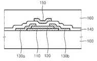
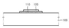
도 1a 및 도 1b는 본 발명의 제1 실시예에 따른 박막 트랜지스터(이하, 본 발명의 제1 박막 트랜지스터)를 보여준다.1A and 1B show a thin film transistor (hereinafter referred to as a first thin film transistor of the present invention) according to the first embodiment of the present invention.
본 발명의 제1 박막 트랜지스터는 게이트 전극(150)이 채널층(110) 위에 형성된 탑(Top) 게이트 구조이다.The first thin film transistor of the present invention is a top gate structure in which a
도 1a 및 도 1b를 참조하면, 기판(100) 상에 채널층(110)이 형성되어 있다. 기판(100)은 실리콘 기판, 유리 기판 및 플라스틱 기판 중 하나일 수 있고, 투명하 거나 불투명할 수 있다. 채널층(110)은 산화물 반도체 물질층, 예컨대 Zn0 계열의 물질층일 수 있다. 상기 ZnO 계열의 물질층은, 예컨대 Ga-In-Zn-O층일 수 있다. 상기 Ga-In-Zn-O층은 a(In2O3)·b(Ga2O3)·c(ZnO)층일 수 있다. 여기서, a, b, c는 각각 a≥0, b≥0, c>0의 조건을 만족하는 실수일 수 있다. 보다 구체적으로, a, b, c는 각각 a≥1, b≥1, 0<c≤1의 조건을 만족하는 실수일 수 있다. 상기 Ga-In-Zn-O층은 스퍼터링(sputtering) 법 및 증발(evaporation) 법을 포함하는 물리 기상 증착(Physical Vapor Deposition)(PVD) 방법으로 형성된 것일 수 있다.Referring to FIGS. 1A and 1B, a
채널층(110) 상에 서로 마주보며 위치하는 소오스 전극(130a) 및 드레인 전극(130b)이 형성되어 있다. 소오스 전극(130a) 및 드레인 전극(130b)은 각각 채널층(110) 둘레의 기판(100) 상으로 연장될 수 있다. 소오스 전극(130a) 및 드레인 전극(130b)은 금속층으로 형성딘 것일 수 있다. 이때 상기 금속층은, 예컨대, Mo 단일 금속층, Mo층을 포함하는 다중 금속층, Ti를 포함하는 금속층 및 Cr을 포함하는 금속층 중 어느 하나일 수 있다.A
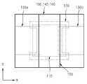
채널층(110) 상에 보호층(120)이 존재한다. 보호층(120)은 채널층(110)에서 소오스/드레인 전극(130a, 130b)과 접촉되는 부분을 제외한 나머지 부분을 덮는다. 보호층(120)의 일부분은 채널층(110) 둘레의 기판(100) 상으로 확장되어 있다. 소오스/드레인 전극(130a, 130b)은 이러한 보호층(120) 상으로 확장되어 있다. 보호층(120)은 채널층(110)과 소오스 전극(130a)이 접촉하는 제1 콘택 영역 및 채널층(110)과 드레인 전극(130b)이 접촉하는 제2 콘택 영역을 제공할 수 있다. 상기 제1 및 제2 콘택 영역은 채널층(110) 상면의 양단일 수 있다. 다시 말해, 보호층(120)은 채널층(110) 상면의 상기 양단을 제외한 나머지 영역을 덮도록 형성될 수 있다. 이에 따라, 도 1b에 도시된 바와 같이, 보호층(120)은 아령 모양이 될 수 있다. 이러한 보호층(120)에 의해 채널층(110)의 상기 양단의 중앙부가 노출된다. 보호층(120)의 모양은 아령 모양으로 제한되지 않고 다양하게 변형될 수 있다. 예컨대, 보호층(120)은 채널층(110)을 Y축 방향으로 가로지르는 사각형일 수도 있다. 또한, 도 1b에 도시된 바와 같이, 보호층(120)은 그 일부가 채널층(110)의 외측으로 연장될 수 있지만, 보호층(120)이 채널층(110)의 외측으로 연장되지 않을 수도 있다. 채널층(110)의 상면은 보호층(120), 소오스 전극(130a) 및 드레인 전극(130b)에 의해 덮여진다.There is a
기판(100) 상에 채널층(110), 보호층(120), 소오스 전극(130a) 및 드레인 전극(130b)을 덮는 게이트 절연층(140)이 형성되어 있다. 게이트 절연층(140)은 실리콘 산화물층이나 실리콘 질화물층일 수 있다. 채널층(110) 위쪽의 게이트 절연층(140) 상에 게이트 전극(150)이 형성되어 있다. 게이트 전극(150)은 소오스 전극(130a)과 동일한 금속으로 형성된 전극일 수 있으나, 다른 금속으로 형성된 것일 수도 있다. 게이트 절연층(140) 상에 게이트 전극(150)을 덮는 패시베이션층(passivation layer)(160)이 형성되어 있다. 패시베이션층(160)은 실리콘 산화물층이나 실리콘 질화물층일 수 있다.A
채널층(110), 소오스 전극(130a), 드레인 전극(130b), 게이트 절연층(140) 및 게이트 전극(150)의 두께는 각각 30∼200nm, 10∼200nm, 10∼200nm, 100∼300nm 및 100∼300nm 정도일 수 있다.The thicknesses of the
도시하지는 않았지만, 채널층(110)과 소오스 전극(130a) 사이 및 채널층(110)과 드레인 전극(130b) 사이에 각각 오믹 콘택층이 더 구비될 수 있다. 상기 오믹 콘택층은 채널층(110)보다 산소 함량이 적은 전도성 산화물층일 수 있다. 상기 오믹 콘택층은 채널층(110)과 소오스 전극(130a) 및 드레인 전극(130b) 간의 접촉 저항을 낮추고, 홀(hole)이 채널층(110) 외부로 빠져나가는 것을 방지하는 역할을 한다.Although not shown, an ohmic contact layer may be further provided between the
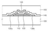
도 2a 및 도 2b는 본 발명의 제2 실시예에 따른 박막 트랜지스터(이하, 본 발명의 제2 박막 트랜지스터)를 보여준다. 본 발명의 제2 박막 트랜지스터는 게이트 전극(250)이 채널층(210) 아래에 형성된 바텀(Bottom) 게이트 구조이다.2A and 2B show a thin film transistor (hereinafter referred to as a second thin film transistor of the present invention) according to a second embodiment of the present invention. The second thin film transistor of the present invention is a bottom gate structure in which the
도 2a 및 도 2b를 참조하면, 기판(200) 상에 게이트 전극(250)이 형성되어 있고, 기판(200) 상에 게이트 전극(250)을 덮는 게이트 절연층(240)이 형성되어 있다. 게이트 전극(250) 위쪽의 게이트 절연층(240) 상에 채널층(210)이 형성되어 있다. X축 방향으로의 채널층(210)의 폭(w1)이 게이트 전극(250)의 폭(w2)보다 큰 것이 바람직하다. 채널층(210)의 일부를 제외한 나머지 영역을 덮는 보호층(220)이 채널층(210) 상에 형성되어 있다. 보호층(220)은 아령 모양으로 형성되어 채널층(210) 양단의 중앙부를 노출시킨다. 보호층(220)의 모양은 다양하게 변형될 수 있다. 보호층(220)의 일부는 채널층(210) 외측의 게이트 절연층(240) 상으로 연장될 수 있다. 소오스 전극(230a) 및 드레인 전극(230b)이 채널층(210)의 상기 양단의 중앙부에 각각 접촉되도록 형성되어 있다. 소오스 전극(230a) 및 드레인 전 극(230b)의 일부는 보호층(220) 상으로 확장되어 있다. 채널층(210)의 상면은 보호층(220), 소오스 전극(230a) 및 드레인 전극(230b)에 의해 덮여져 있다. 게이트 절연층(240) 상에 채널층(210), 보호층(220), 소오스 전극(230a) 및 드레인 전극(230b)을 덮는 패시베이션층(260)이 형성되어 있다.2A and 2B, a
도 2a 및 도 2b의 기판(200), 채널층(210), 보호층(220), 소오스 전극(230a), 드레인 전극(230b), 게이트 절연층(240), 게이트 전극(250) 및 패시베이션층(260) 각각의 재질 및 두께는 도 1a 및 도 1b의 기판(100), 채널층(110), 보호층(120), 소오스 전극(130a), 드레인 전극(130b), 게이트 절연층(140), 게이트 전극(150) 및 패시베이션층(160) 각각의 그것들과 동일할 수 있다.The
도시하지는 않았지만, 채널층(210)과 소오스 전극(230a) 사이 및 채널층(210)과 드레인 전극(230b) 사이에 각각 오믹 콘택층이 더 구비될 수 있다. 상기 오믹 콘택층은 채널층(210)보다 산소 함량이 적은 전도성 산화물층일 수 있다.An ohmic contact layer may be further provided between the
도 3a 내지 도 3e는 본 발명의 제1 실시예에 따른 박막 트랜지스터의 제조방법(이하, 본 발명의 제1 방법)을 보여준다. 본 발명의 제1 방법은 탑 게이트 구조의 박막 트랜지스터의 제조방법이다. 도 1a 및 도 1b와 도 3a 내지 도 3e에서 동일한 참조 번호(부호)는 동일한 구성 요소를 나타낸다.3A to 3E show a method of manufacturing a thin film transistor (hereinafter, a first method of the present invention) according to the first embodiment of the present invention. A first method of the present invention is a method of manufacturing a thin film transistor of a top gate structure. The same reference numerals in Figs. 1A and 1B and Figs. 3A to 3E denote the same elements.
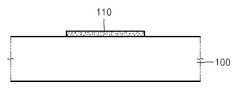
도 3a를 참조하면, 기판(100) 상에 채널층(110)을 형성한다. 채널층(110)은 Ga-In-Zn-O와 같은 산화물 반도체로 형성할 수 있는데, 스퍼터링(sputtering) 법 및 증발(evaporation) 법을 포함하는 물리 기상 증착(Physical Vapor Deposition)(PVD) 방법으로 형성할 수 있다. 상기 PVD 방법을 이용한 채널층(110) 의 형성에 한 개 이상의 타겟이 사용될 수 있다. 상기 한 개 이상의 타겟은 In2O3, Ga2O3 및 ZnO 중 적어도 하나를 포함할 수 있다. 채널층(110) 형성 후, 채널층(110)의 표면을 산소 플라즈마로 처리할 수 있다. 이렇게 함으로써, 채널층(110) 표면의 산소 농도가 증가하여 채널층(110) 표면부의 전기 저항이 증가할 수 있다. 채널층(110) 표면부의 전기 저항이 증가되면, 후속 공정에서 채널층(110) 표면부의 특성이 열화되는 것을 줄일 수 있다. 상기 산소 플라즈마 처리 후, 기판(100) 및 채널층(110)의 상면에 존재하는 식각 부산물들을 제거하기 위한 습식 세정을 수행할 수 있다. 상기 습식 세정에서 세정액으로는 IPA(isopropyl alcohol)와 탈이온수(deionized water) 및 아세톤(aceton) 중 적어도 어느 하나를 사용할 수 있다.Referring to FIG. 3A, a
도 3b를 참조하면, 채널층(110) 상에 채널층(110)의 마주하는 두 영역을 제외한 나머지 부분을 덮는 보호층(120)을 형성한다. 보호층(120)은 그 일부가 기판(100) 상으로 확장되게 형성할 수 있다. 이러한 보호층(120)은 기판(100) 상에 보호 물질막(미도시)을 형성한 후, 채널층(110)의 마주하는 두 영역, 예컨대 채널층(110) 상면의 양단을 제외한 나머지 부분이 노출되도록 상기 보호 물질층을 패터닝하여 형성할 수 있다. 보호층(120)은 CVD(chemical vapor deposition) 또는 PVD 방법을 이용해서 실리콘 산화물층 또는 실리콘 질화물층으로 형성할 수 있다.Referring to FIG. 3B, a
본 발명의 제1 방법에서 상술한 채널층(110)과 보호층(120)의 형성방법을 채널층(110)과 보호층(120)의 제1 형성방법이라고 한다.The method of forming the
도 3c를 참조하면, 기판(100) 상에 채널층(110) 및 보호층(120)을 덮는 금속 층(130)을 형성한다. 금속층(130) 상에 소오스/드레인 영역을 한정하는 마스크(M)를 형성한다. 마스크(M) 둘레의 금속층(130)을 제거한다. 이때, 금속층(130)은 습식 또는 건식 식각 방법으로 제거할 수 있다. 이후 마스크(M)를 제거한다. 이렇게 해서, 도 3d에 도시한 바와 같이, 채널층(110)의 상기 양단과 각각 접촉된 소오스 전극(130a)과 드레인 전극(130b)이 형성된다. 금속층(130)은 Mo 단일 금속층, Mo층을 포함하는 다중 금속층, Ti를 포함하는 금속층 및 Cr을 포함하는 금속층 중 어느 하나일 수 있다. 금속층(130)은 PVD 방법으로 형성할 수 있다. 금속층(130)을 습식 식각 방법으로 제거할 때, 에천트(etchant)로서 인산(H3PO4), 초산(CH3COOH), 질산(HNO3) 및 탈이온수의 혼합액을 사용할 수 있다.Referring to FIG. 3C, a
보호층(120)이 형성되어 있기 때문에, 소오스 전극(130a) 및 드레인 전극(130b)을 형성하기 위한 식각 공정시 채널층(110)의 손상 및 특성 열화가 방지된다. 보다 구체적으로 설명하면, 소오스 전극(130a) 및 드레인 전극(130b)용 금속층을 습식 식각 방법으로 식각하는 경우, 상기 금속층과 채널층(110) 간의 식각 선택비가 없어도 상기 금속층의 패터닝이 가능하다. 또한 소오스 전극(130a) 및 드레인 전극(130b)용 금속층을 건식 식각 방법으로 식각하는 경우, 상기 건식 식각시 사용되는 플라즈마에 의한 채널층(110)의 특성 열화가 방지된다.Since the
소오스 전극(130a)과 드레인 전극(130b)을 고온에서 형성하면, 소오스 전극(130a)과 드레인 전극(130b)을 형성하는 과정에서 채널층(110)과 소오스 전극(130a) 및 드레인 전극(130b) 사이에 채널층(110)보다 산소 함량이 적은 오믹 콘 택층(미도시)을 형성할 수 있다. 소오스 전극(130a)과 드레인 전극(130b)을 형성하는 과정에서 상기 오믹 콘택층이 형성되지 않을 때, 후속으로 어닐링 공정을 실시할 수 있다. 상기 어닐링 공정에 의해 채널층(110)과 소오스 전극(130a) 및 드레인 전극(130b) 사이에 반응이 일어나고, 그 결과 상기 오믹 콘택층이 형성될 수 있다. 상기 어닐링 공정은 퍼니스 어닐링(furnace annealing) 또는 급속 가열 어닐링(rapid thermal annealing : RTA)일 수 있는데, 산소 또는 질소 분위기에서 200∼400℃의 온도로 10분∼2시간 동안 수행할 수 있다.When the source and
소오스 전극(130a)과 드레인 전극(130b)을 형성하는 과정에서 상기 오믹 콘택층을 형성하지 않고, 다른 시점에서 다른 방법으로 오믹 콘택층(미도시)을 형성할 수도 있다. 예를 들어, 금속층(130)을 형성하기 전에, 기판(100) 상에 채널층(110)과 보호층(120)을 덮는 오믹 콘택 물질층(미도시)을 형성할 수 있다. 상기 오믹 콘택 물질층은 채널층(110)보다 산소 함량이 적은 Ga-In-Zn-O층일 수 있는데, 산소 가스를 사용하지 않는 PVD 방법으로 형성할 수 있다. 상기 오믹 콘택 물질층은 금속층(130)과 동일한 형태로 패터닝될 수 있다.In the process of forming the source and
도 3e를 참조하면, 기판(100) 상에 보호층(120), 소오스 전극(130a) 및 드레인 전극(130b)을 덮는 게이트 절연층(140)을 형성한다. 게이트 절연층(140)은 PECVD(plasma enhanced chemical vapor deposition) 방법으로 형성할 수 있다. 게이트 절연층(140)은 실리콘 산화물층 또는 실리콘 질화물층으로 형성할 수 있다. 계속해서, 게이트 절연층(140) 상에 게이트 전극(150)을 형성한다. 게이트 전극(150)은 채널층(110) 위에 위치하도록 형성한다. 게이트 전극(150)은 소오스 전 극(130a) 및 드레인 전극(130b)과 동일한 금속 또는 다른 금속으로 형성할 수 있다. 그 다음, 게이트 절연층(140) 상에 게이트 전극(150)을 덮는 패시베이션층(160)을 형성한다.패시베이션층(160)은 실리콘 산화물층 또는 실리콘 질화물층으로 형성할 수 있다.Referring to FIG. 3E, a
도 4a 내지 도 4f는 본 발명의 제2 실시예에 따른 박막 트랜지스터의 제조방법(이하, 본 발명의 제2 방법)을 보여준다.4A to 4F show a method of manufacturing a thin film transistor (hereinafter, a second method of the present invention) according to a second embodiment of the present invention.
본 발명의 제1 방법과 본 발명의 제2 방법의 차이는 채널층(110) 및 보호층(120)의 형성방법에 있다.The difference between the first method of the present invention and the second method of the present invention lies in the method of forming the
본 발명의 제1 방법에서는 채널층(110)과 보호층(120)을 별개의 포토 마스크를 사용하여 형성하였지만, 본 발명의 제2 방법에서는 채널층(110)과 보호층(120)을 하나의 포토 마스크, 예컨대, 하나의 하프톤 포토 마스크 또는 하나의 슬릿 포토 마스크를 사용하여 형성할 수 있다.In the first method of the present invention, the
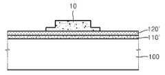
도 4a를 참조하면, 기판(100) 상에 산화물 반도체막(110')을 형성한다. 산화물 반도체막(110') 상에 보호 물질막(120')을 형성한다. 산화물 반도체막(110')과 보호 물질막(120')은 PVD 방법으로 연속해서 증착할 수 있다. 다른 방법으로는 PVD 방법으로 산화물 반도체막(110')을 형성한 후, CVD 방법으로 보호 물질막(120')을 형성할 수도 있다. 산화물 반도체막(110')의 형성 후, 보호 물질막(120')을 형성하기 전에, 산화물 반도체막(110')의 표면을 산소 플라즈마로 처리할 수 있다.Referring to FIG. 4A, an oxide semiconductor film 110 'is formed on a
그 다음, 보호 물질막(120') 상에 감광층을 도포한 후, 상기 감광층을 하프톤 포토 마스크 또는 슬릿 포토 마스크를 사용해서 패터닝한다. 그 결과, 도 4a에 도시된 바와 같은, 채널층 형성 영역을 한정하는 감광층 패턴(10)이 형성된다. 감광층 패턴(10)은 영역에 따라 서로 다른 두께를 갖는다. 감광층 패턴(10)의 중앙부의 두께가 두꺼운 영역은 제1 영역이라 하고, 양측 가장자리의 두께가 얇은 영역은 제2 영역이라 한다.Next, a photosensitive layer is coated on the protective material film 120 ', and then the photosensitive layer is patterned using a halftone photomask or a slit photomask. As a result, the
도 4b를 참조하면, 감광층 패턴(10)을 식각 마스크로 이용해서 보호 물질막(120')과 산화물 반도체막(110')을 순차로 식각한다. 이러한 식각 후에 남은 산화물 반도체막(110)은 채널층이 된다.Referring to FIG. 4B, the protective material layer 120 'and the oxide semiconductor layer 110' are sequentially etched using the
계속해서, 감광층 패턴(10)을 산소 에싱(ashing)과 같은 방법으로 등방성 식각하여 상기 제2 영역을 제거한다. 이 결과, 도 4c에 도시한 바와 같이, 감광막 패턴(10)의 제1 영역 둘레의 보호 물질막(120')이 노출된다. 상기 제2 영역이 제거되는 동안 상기 제1 영역의 일부 두께도 제거된다.Subsequently, the
도 4c를 참조하면, 감광층 패턴(10)을 식각 마스크로 이용해서 보호 물질막(120')의 노출된 부분을 식각한다. 이후, 감광층 패턴(10)을 제거한다. 이 결과, 도 4d에 도시된 바와 같이 채널층(110) 상에 채널층(110)의 마주하는 두 영역을 노출시키는 보호층(120)이 형성된다. 보호층(120)의 이러한 형태는 상기 제2 영역이 제거된 감광막 패턴(10)에 의해 결정된다. 그러므로 도 4a의 감광막 패턴(10)을 이점을 고려하여 형성한다.Referring to FIG. 4C, the exposed portion of the protective material layer 120 'is etched using the
보호층(120)은 채널층(110) 상면의 양단, 또는 상기 양단의 중앙부를 노출시키지만, 채널층(110)의 외측으로 연장되지 않는다.The
본 발명의 제2 방법에서 기재된 채널층(110)과 보호층(120)의 형성방법을 채 널층과 보호층의 제2 형성방법이라고 한다.The method of forming the
도 4e를 참조하면, 기판(100) 상에 채널층(110)의 상기 노출된 두 영역을 각각 덮는 소오스/드레인 전극(130a, 130b)을 형성한다. 소오스/드레인 전극(130a, 130b)은 도 3c에서 설명한 공정과 동일한 공정으로 형성할 수 있다. 단, 도 4e의 경우, 채널층(110)의 측면 일부가 노출되어 있기 때문에, 소오스 전극(130a) 및 드레인 전극(130b)을 형성하는 과정에서 채널층(110)의 측면 방향으로 손실이 발생할 수 있다. 하지만 상기 손실은 무시할 수 있을 정도로 적다. 또한 도 4a 단계에서 채널층(110) 측면의 손실을 감안하여 감광층 패턴(10)을 형성할 수도 있기 때문에, 상기 손실은 나타나지 않을 수도 있다.Referring to FIG. 4E, source /
도 4f를 참조하면, 도 3d를 참조하여 설명한 공정과 동일한 공정을 수행하여 게이트 절연층(140), 게이트 전극(150) 및 패시베이션층(160)을 차례로 형성한다.Referring to FIG. 4F, the
도 5a 내지 도 5d는 본 발명의 제3 실시예에 따른 박막 트랜지스터의 제조방법(이하, 본 발명의 제3 방법)을 보여준다.5A to 5D show a method of manufacturing a thin film transistor (hereinafter, a third method of the present invention) according to a third embodiment of the present invention.
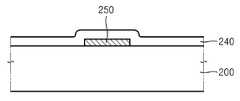
본 발명의 제3 방법은 바텀 게이트 구조의 박막 트랜지스터의 제조방법이다. 도 2a 및 도 2b와 도 5a 내지 도 5d에서 동일한 참조 번호(부호)는 동일한 구성 요소를 나타낸다.A third method of the present invention is a method of manufacturing a thin film transistor of a bottom gate structure. The same reference numerals in FIGS. 2A and 2B and FIGS. 5A to 5D denote the same components.
도 5a를 참조하면, 기판(200) 상에 게이트 전극(250)을 형성하고, 기판(200) 상에 게이트 전극(250)을 덮는 게이트 절연층(240)을 형성한다. 게이트 절연층(240) 형성 후, 게이트 절연층(240) 상면에 존재하는 불순물들을 제거하기 위한 습식 세정을 수행할 수 있다. 상기 습식 세정에서 세정액으로는 IPA(isopropyl alcohol)와 탈이온수(deionized water) 및 아세톤(aceton) 중 적어도 어느 하나를 사용할 수 있다.5A, a
도 5b를 참조하면, 게이트 절연층(240) 상에 순차로 적층된 채널층(210)과 보호층(220)을 형성한다. 채널층(210)은 게이트 전극(250) 위쪽의 게이트 절연층(240) 상에 위치한다. 채널층(210)과 보호층(220)은 상기 채널층과 보호층의 제1 형성방법 또는 상기 채널층과 보호층의 제2 형성방법으로 형성할 수 있다.Referring to FIG. 5B, a
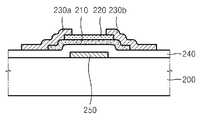
도 5c를 참조하면, 게이트 절연층(240) 및 보호층(220) 상에 채널층(210)의 양단과 각각 접하는 소오스 전극(230a) 및 드레인 전극(230b)을 형성한다. 소오스 전극(230a) 및 드레인 전극(230b)은 도 3c에서 설명한 공정으로 형성할 수 있다. 또한 채널층(210)과 소오스 전극(230a) 및 드레인 전극(230b) 사이에 채널층(210)보다 산소 함량이 적은 오믹 콘택층(미도시)을 형성하는 공정도 상술한 바와 같을 수 있다.5C, a
도 5d를 참조하면, 게이트 절연층(240) 상에 보호층(220), 소오스 전극(230a) 및 드레인 전극(230b)을 덮는 패시베이션층(260)을 형성한다.Referring to FIG. 5D, a
도 6은 본 발명의 제3 방법으로 제조한 박막 트랜지스터의 드레인 전압(Vd)별(0.1V, 5.1V, 10.1V) 게이트 전압(Vg)-드레인 전류(Id)의 특성을 보여준다.6 shows characteristics of the gate voltage (Vg ) -drain current (Id ) according to the drain voltage (Vd ) (0.1 V, 5.1 V, 10.1 V) of the thin film transistor manufactured by the third method of the present invention.
도 6을 참조하면, 본 발명의 방법으로 제조한 박막 트랜지스터는 10.1V 정도의 높은 Vd에서도 우수한 스위칭 특성을 나타내는 것을 확인할 수 있다. 이것은 본 발명의 박막 트랜지스터 제조시 채널층(210)의 손상 및 특성 열화가 방지되었음을 의미한다.Referring to FIG. 6, it can be seen that the thin film transistor manufactured by the method of the present invention exhibits excellent switching characteristics even at a high Vd of about 10.1 V. This means that the damage and characteristic deterioration of the
상기한 설명에서 많은 사항이 구체적으로 기재되어 있으나, 그들은 발명의 범위를 한정하는 것이라기보다, 바람직한 실시예의 예시로서 해석되어야 한다. 예들 들어, 본 발명이 속하는 기술 분야에서 통상의 지식을 가진 자라면, 본 발명의 박막 트랜지스터의 구성 요소는 다양화할 수 있을 것이고, 구조 또한 다양한 형태로 변형할 수 있을 것이다. 또한, 본 발명의 박막 트랜지스터는 액정표시장치나 유기발광표시장치뿐만 아니라 메모리 소자 및 논리 소자 분야에도 적용될 수 있음을 알 수 있을 것이다. 때문에 본 발명의 범위는 설명된 실시예에 의하여 정하여 질 것이 아니고 특허 청구범위에 기재된 기술적 사상에 의해 정하여져야 한다.Although a number of matters have been specifically described in the above description, they should be interpreted as examples of preferred embodiments rather than limiting the scope of the invention. For example, those skilled in the art will appreciate that the elements of the thin film transistor of the present invention can be varied and the structure can be modified into various forms. It will also be understood that the thin film transistor of the present invention can be applied not only to liquid crystal display devices and organic light emitting display devices but also to memory devices and logic devices. Therefore, the scope of the present invention is not to be determined by the described embodiments but should be determined by the technical idea described in the claims.
이상에서 설명한 바와 같이, 본 발명의 박막 트랜지스터의 산화물 반도체 물질로 형성된 채널층은 소오스/드레인 전극과 접촉되는 영역을 제외한 나머지 부분이 보호층으로 덮여 있기 때문에, 소오스 전극 및 드레인 전극을 형성하기 위한 식각 공정에서 채널층의 손상 및 특성 열화를 방지할 수 있다. 따라서, 본 발명을 이용하면 이동도가 높은 산화물 반도체 물질, 예컨대, Ga-In-Zn-O로 형성된 채널층을 갖는 박막 트랜지스터를 구현할 수 있다.As described above, since the channel layer formed of the oxide semiconductor material of the thin film transistor of the present invention is covered with the protective layer except the region in contact with the source / drain electrode, the etching for forming the source electrode and the drain electrode It is possible to prevent damage and deterioration of the channel layer in the process. Therefore, the present invention can realize a thin film transistor having a channel layer formed of an oxide semiconductor material having high mobility, for example, Ga-In-Zn-O.
Claims (29)
Translated fromKoreanPriority Applications (5)
| Application Number | Priority Date | Filing Date | Title |
|---|---|---|---|
| KR1020070016778AKR101410926B1 (en) | 2007-02-16 | 2007-02-16 | Thin film transistor and manufacturing method thereof |
| US12/005,395US7910920B2 (en) | 2007-02-16 | 2007-12-27 | Thin film transistor and method of forming the same |
| JP2008034171AJP5572290B2 (en) | 2007-02-16 | 2008-02-15 | Thin film transistor and manufacturing method thereof |
| CN200810074302.8ACN101246909B (en) | 2007-02-16 | 2008-02-15 | Thin film transistor and method of forming the same |
| US12/929,818US8614442B2 (en) | 2007-02-16 | 2011-02-17 | Thin film transistor and method of forming the same |
Applications Claiming Priority (1)
| Application Number | Priority Date | Filing Date | Title |
|---|---|---|---|
| KR1020070016778AKR101410926B1 (en) | 2007-02-16 | 2007-02-16 | Thin film transistor and manufacturing method thereof |
Related Child Applications (1)
| Application Number | Title | Priority Date | Filing Date |
|---|---|---|---|
| KR1020130133002ADivisionKR101438642B1 (en) | 2013-11-04 | 2013-11-04 | Thin film transistor and method for forming the same |
Publications (2)
| Publication Number | Publication Date |
|---|---|
| KR20080076608A KR20080076608A (en) | 2008-08-20 |
| KR101410926B1true KR101410926B1 (en) | 2014-06-24 |
Family
ID=39705862
Family Applications (1)
| Application Number | Title | Priority Date | Filing Date |
|---|---|---|---|
| KR1020070016778AActiveKR101410926B1 (en) | 2007-02-16 | 2007-02-16 | Thin film transistor and manufacturing method thereof |
Country Status (4)
| Country | Link |
|---|---|
| US (2) | US7910920B2 (en) |
| JP (1) | JP5572290B2 (en) |
| KR (1) | KR101410926B1 (en) |
| CN (1) | CN101246909B (en) |
Families Citing this family (137)
| Publication number | Priority date | Publication date | Assignee | Title |
|---|---|---|---|---|
| JP2008277326A (en)* | 2007-04-25 | 2008-11-13 | Canon Inc | Amorphous oxide semiconductor, semiconductor device and thin film transistor |
| EP2183780A4 (en)* | 2007-08-02 | 2010-07-28 | Applied Materials Inc | THIN FILM TRANSISTORS USING THIN FILM SEMICONDUCTOR MATERIALS |
| JP4759598B2 (en)* | 2007-09-28 | 2011-08-31 | キヤノン株式会社 | THIN FILM TRANSISTOR, MANUFACTURING METHOD THEREOF, AND DISPLAY DEVICE USING THE SAME |
| JP5325446B2 (en)* | 2008-04-16 | 2013-10-23 | 株式会社日立製作所 | Semiconductor device and manufacturing method thereof |
| JP2010056541A (en) | 2008-07-31 | 2010-03-11 | Semiconductor Energy Lab Co Ltd | Semiconductor device and manufacturing method thereof |
| TWI627757B (en) | 2008-07-31 | 2018-06-21 | 半導體能源研究所股份有限公司 | Semiconductor device |
| TWI469354B (en) | 2008-07-31 | 2015-01-11 | Semiconductor Energy Lab | Semiconductor device and method of manufacturing same |
| JP5616038B2 (en) | 2008-07-31 | 2014-10-29 | 株式会社半導体エネルギー研究所 | Method for manufacturing semiconductor device |
| KR101516050B1 (en) | 2008-08-27 | 2015-05-04 | 이데미쓰 고산 가부시키가이샤 | Field-effect transistor, method for manufacturing same, and sputtering target |
| US9082857B2 (en) | 2008-09-01 | 2015-07-14 | Semiconductor Energy Laboratory Co., Ltd. | Semiconductor device comprising an oxide semiconductor layer |
| WO2010029865A1 (en)* | 2008-09-12 | 2010-03-18 | Semiconductor Energy Laboratory Co., Ltd. | Display device |
| KR101767864B1 (en)* | 2008-09-12 | 2017-08-11 | 가부시키가이샤 한도오따이 에네루기 켄큐쇼 | Semiconductor device and manufacturing method thereof |
| KR101657957B1 (en)* | 2008-09-12 | 2016-09-20 | 가부시키가이샤 한도오따이 에네루기 켄큐쇼 | Display device |
| JP4623179B2 (en)* | 2008-09-18 | 2011-02-02 | ソニー株式会社 | Thin film transistor and manufacturing method thereof |
| CN102160184B (en) | 2008-09-19 | 2014-07-09 | 株式会社半导体能源研究所 | Display device |
| CN102160103B (en) | 2008-09-19 | 2013-09-11 | 株式会社半导体能源研究所 | Display device |
| KR101670695B1 (en) | 2008-09-19 | 2016-10-31 | 가부시키가이샤 한도오따이 에네루기 켄큐쇼 | Semiconductor device |
| KR101803264B1 (en)* | 2008-09-19 | 2017-12-28 | 가부시키가이샤 한도오따이 에네루기 켄큐쇼 | Semiconductor device |
| CN102160105B (en)* | 2008-09-19 | 2014-06-11 | 株式会社半导体能源研究所 | Display device and manufacturing method thereof |
| JPWO2010038566A1 (en)* | 2008-09-30 | 2012-03-01 | コニカミノルタホールディングス株式会社 | Thin film transistor and manufacturing method thereof |
| EP2172977A1 (en)* | 2008-10-03 | 2010-04-07 | Semiconductor Energy Laboratory Co., Ltd. | Display device |
| CN101714546B (en) | 2008-10-03 | 2014-05-14 | 株式会社半导体能源研究所 | Display device and manufacturing method thereof |
| KR101435501B1 (en) | 2008-10-03 | 2014-08-29 | 가부시키가이샤 한도오따이 에네루기 켄큐쇼 | Display device |
| JP5552753B2 (en)* | 2008-10-08 | 2014-07-16 | ソニー株式会社 | Thin film transistor and display device |
| US8106400B2 (en) | 2008-10-24 | 2012-01-31 | Semiconductor Energy Laboratory Co., Ltd. | Semiconductor device and method for manufacturing the same |
| EP2180518B1 (en)* | 2008-10-24 | 2018-04-25 | Semiconductor Energy Laboratory Co, Ltd. | Method for manufacturing semiconductor device |
| KR20160072845A (en) | 2008-10-24 | 2016-06-23 | 가부시키가이샤 한도오따이 에네루기 켄큐쇼 | Semiconductor device and method for manufacturing the same |
| US8741702B2 (en)* | 2008-10-24 | 2014-06-03 | Semiconductor Energy Laboratory Co., Ltd. | Method for manufacturing semiconductor device |
| KR101586674B1 (en)* | 2008-10-28 | 2016-01-20 | 엘지디스플레이 주식회사 | Manufacturing method of oxide thin film transistor |
| TWI467663B (en)* | 2008-11-07 | 2015-01-01 | Semiconductor Energy Lab | Semiconductor device and method of manufacturing the same |
| TWI656645B (en)* | 2008-11-13 | 2019-04-11 | 日商半導體能源研究所股份有限公司 | Semiconductor device and method of manufacturing same |
| KR101432764B1 (en)* | 2008-11-13 | 2014-08-21 | 가부시키가이샤 한도오따이 에네루기 켄큐쇼 | Method for manufacturing semiconductor device |
| JP5123141B2 (en) | 2008-11-19 | 2013-01-16 | 株式会社東芝 | Display device |
| JP2010153802A (en) | 2008-11-20 | 2010-07-08 | Semiconductor Energy Lab Co Ltd | Semiconductor device and method of manufacturing the same |
| KR101914404B1 (en) | 2008-11-21 | 2018-11-01 | 가부시키가이샤 한도오따이 에네루기 켄큐쇼 | Semiconductor device |
| JP2010140919A (en)* | 2008-12-09 | 2010-06-24 | Hitachi Ltd | Oxide semiconductor device, manufacturing method thereof, and active matrix substrate |
| WO2010071183A1 (en)* | 2008-12-19 | 2010-06-24 | Semiconductor Energy Laboratory Co., Ltd. | Method for manufacturing semiconductor device |
| TWI501319B (en) | 2008-12-26 | 2015-09-21 | Semiconductor Energy Lab | Semiconductor device and manufacturing method thereof |
| JP2010182819A (en)* | 2009-02-04 | 2010-08-19 | Sony Corp | Thin-film transistor, and display device |
| CN101840936B (en)* | 2009-02-13 | 2014-10-08 | 株式会社半导体能源研究所 | Semiconductor device including a transistor, and manufacturing method of the semiconductor device |
| US8278657B2 (en)* | 2009-02-13 | 2012-10-02 | Semiconductor Energy Laboratory Co., Ltd. | Transistor, semiconductor device including the transistor, and manufacturing method of the transistor and the semiconductor device |
| US8247812B2 (en) | 2009-02-13 | 2012-08-21 | Semiconductor Energy Laboratory Co., Ltd. | Transistor, semiconductor device including the transistor, and manufacturing method of the transistor and the semiconductor device |
| US8461582B2 (en)* | 2009-03-05 | 2013-06-11 | Semiconductor Energy Laboratory Co., Ltd. | Semiconductor device and method for manufacturing the same |
| JP5504008B2 (en) | 2009-03-06 | 2014-05-28 | 株式会社半導体エネルギー研究所 | Semiconductor device |
| JP2010263182A (en) | 2009-04-10 | 2010-11-18 | Toppan Printing Co Ltd | Thin film transistor and image display device |
| KR101579453B1 (en)* | 2009-04-29 | 2015-12-24 | 삼성디스플레이 주식회사 | Thin film transistor substrate and method of fabricating thereof |
| EP2256795B1 (en)* | 2009-05-29 | 2014-11-19 | Semiconductor Energy Laboratory Co., Ltd. | Manufacturing method for oxide semiconductor device |
| EP2256814B1 (en) | 2009-05-29 | 2019-01-16 | Semiconductor Energy Laboratory Co, Ltd. | Oxide semiconductor device and method for manufacturing the same |
| JP5564331B2 (en)* | 2009-05-29 | 2014-07-30 | 株式会社半導体エネルギー研究所 | Method for manufacturing semiconductor device |
| KR102503687B1 (en) | 2009-07-03 | 2023-02-27 | 가부시키가이샤 한도오따이 에네루기 켄큐쇼 | Method for manufacturing semiconductor device |
| KR102798889B1 (en)* | 2009-07-10 | 2025-04-23 | 가부시키가이샤 한도오따이 에네루기 켄큐쇼 | Method for manufacturing liquid crystal display device |
| KR101739154B1 (en)* | 2009-07-17 | 2017-05-23 | 가부시키가이샤 한도오따이 에네루기 켄큐쇼 | Semiconductor device and manufacturing method thereof |
| WO2011027649A1 (en) | 2009-09-02 | 2011-03-10 | Semiconductor Energy Laboratory Co., Ltd. | Semiconductor device including a transistor, and manufacturing method of semiconductor device |
| JP5458102B2 (en)* | 2009-09-04 | 2014-04-02 | 株式会社東芝 | Thin film transistor manufacturing method |
| CN102498570B (en) | 2009-09-04 | 2016-02-10 | 株式会社半导体能源研究所 | Light emitting device and manufacturing method thereof |
| WO2011034012A1 (en)* | 2009-09-16 | 2011-03-24 | Semiconductor Energy Laboratory Co., Ltd. | Logic circuit, light emitting device, semiconductor device, and electronic device |
| JP5532803B2 (en)* | 2009-09-30 | 2014-06-25 | ソニー株式会社 | Semiconductor device and display device |
| KR102246127B1 (en) | 2009-10-08 | 2021-04-29 | 가부시키가이샤 한도오따이 에네루기 켄큐쇼 | Semiconductor device |
| JPWO2011043300A1 (en)* | 2009-10-09 | 2013-03-04 | シャープ株式会社 | Semiconductor device and manufacturing method thereof |
| CN102598278B (en)* | 2009-10-09 | 2015-04-08 | 株式会社半导体能源研究所 | Semiconductor device |
| WO2011043194A1 (en)* | 2009-10-09 | 2011-04-14 | Semiconductor Energy Laboratory Co., Ltd. | Semiconductor device and method for manufacturing the same |
| KR102329380B1 (en)* | 2009-10-09 | 2021-11-22 | 가부시키가이샤 한도오따이 에네루기 켄큐쇼 | Semiconductor device |
| KR101056229B1 (en) | 2009-10-12 | 2011-08-11 | 삼성모바일디스플레이주식회사 | An organic light emitting display device comprising a thin film transistor, a method of manufacturing the same, and a thin film transistor |
| EP2491585B1 (en)* | 2009-10-21 | 2020-01-22 | Semiconductor Energy Laboratory Co. Ltd. | Semiconductor device |
| KR101812683B1 (en)* | 2009-10-21 | 2017-12-27 | 가부시키가이샤 한도오따이 에네루기 켄큐쇼 | Method for manufacturing semiconductor device |
| KR101652790B1 (en) | 2009-11-09 | 2016-08-31 | 삼성전자주식회사 | Transistor, method of manufacturing the same and electronic device comprising transistor |
| KR102393447B1 (en) | 2009-11-13 | 2022-05-03 | 가부시키가이샤 한도오따이 에네루기 켄큐쇼 | Semiconductor device and manufacturing method thereof |
| KR101945660B1 (en) | 2009-11-20 | 2019-02-07 | 가부시키가이샤 한도오따이 에네루기 켄큐쇼 | Transistor |
| KR101370301B1 (en)* | 2009-11-20 | 2014-03-05 | 가부시키가이샤 한도오따이 에네루기 켄큐쇼 | Method for manufacturing semiconductor device |
| TWI395334B (en)* | 2009-11-20 | 2013-05-01 | Au Optronics Corp | Thin film transistor element and manufacturing method thereof |
| KR101802406B1 (en) | 2009-11-27 | 2017-11-28 | 가부시키가이샤 한도오따이 에네루기 켄큐쇼 | Semiconductor device and method for manufacturing the same |
| KR101623961B1 (en)* | 2009-12-02 | 2016-05-26 | 삼성전자주식회사 | Transistor, method of manufacturing the same and electronic device comprising transistor |
| KR101511076B1 (en)* | 2009-12-08 | 2015-04-10 | 가부시키가이샤 한도오따이 에네루기 켄큐쇼 | Semiconductor device and manufacturing method thereof |
| KR101615636B1 (en)* | 2009-12-08 | 2016-04-27 | 삼성전자주식회사 | Transistor and electronic device comprising the transistor |
| KR20110066370A (en) | 2009-12-11 | 2011-06-17 | 한국전자통신연구원 | Thin film transistor and its manufacturing method |
| KR101117727B1 (en) | 2009-12-16 | 2012-03-07 | 삼성모바일디스플레이주식회사 | Organic light emitting display and manufacturing method thereof |
| WO2011074590A1 (en)* | 2009-12-17 | 2011-06-23 | Semiconductor Energy Laboratory Co., Ltd. | Semiconductor device, measurement apparatus, and measurement method of relative permittivity |
| KR101117730B1 (en) | 2009-12-23 | 2012-03-07 | 삼성모바일디스플레이주식회사 | Organic light emitting display and manufacturing method thereof |
| KR101035358B1 (en) | 2010-01-07 | 2011-05-20 | 삼성모바일디스플레이주식회사 | Touch sensor and organic light emitting display |
| US9391209B2 (en) | 2010-02-05 | 2016-07-12 | Semiconductor Energy Laboratory Co., Ltd. | Semiconductor device |
| CN105590964B (en)* | 2010-02-05 | 2019-01-04 | 株式会社半导体能源研究所 | Semiconductor device |
| US8436403B2 (en)* | 2010-02-05 | 2013-05-07 | Semiconductor Energy Laboratory Co., Ltd. | Semiconductor device including transistor provided with sidewall and electronic appliance |
| KR101084192B1 (en) | 2010-02-16 | 2011-11-17 | 삼성모바일디스플레이주식회사 | Organic light emitting display |
| WO2011102233A1 (en)* | 2010-02-19 | 2011-08-25 | Semiconductor Energy Laboratory Co., Ltd. | Semiconductor device |
| KR102838177B1 (en)* | 2010-02-26 | 2025-07-23 | 가부시키가이샤 한도오따이 에네루기 켄큐쇼 | Liquid crystal display device |
| JP5708910B2 (en) | 2010-03-30 | 2015-04-30 | ソニー株式会社 | THIN FILM TRANSISTOR, MANUFACTURING METHOD THEREOF, AND DISPLAY DEVICE |
| CN102208406B (en)* | 2010-03-30 | 2013-07-24 | 元太科技工业股份有限公司 | A pixel structure and its manufacturing method |
| US9190522B2 (en)* | 2010-04-02 | 2015-11-17 | Semiconductor Energy Laboratory Co., Ltd. | Semiconductor device having an oxide semiconductor |
| KR101803730B1 (en) | 2010-04-09 | 2017-12-01 | 가부시키가이샤 한도오따이 에네루기 켄큐쇼 | Semiconductor device |
| WO2011126076A1 (en)* | 2010-04-09 | 2011-10-13 | 大日本印刷株式会社 | Thin-film transistor substrate |
| KR102434906B1 (en)* | 2010-04-23 | 2022-08-23 | 가부시키가이샤 한도오따이 에네루기 켄큐쇼 | Method for manufacturing semiconductor device |
| US9490368B2 (en) | 2010-05-20 | 2016-11-08 | Semiconductor Energy Laboratory Co., Ltd. | Semiconductor device and manufacturing method of the same |
| KR20120000499A (en) | 2010-06-25 | 2012-01-02 | 가부시키가이샤 한도오따이 에네루기 켄큐쇼 | Transistors and Semiconductor Devices |
| KR20250021395A (en) | 2010-07-02 | 2025-02-12 | 가부시키가이샤 한도오따이 에네루기 켄큐쇼 | Semiconductor device and manufacturing method thereof |
| JP5403527B2 (en)* | 2010-07-02 | 2014-01-29 | 合同会社先端配線材料研究所 | Semiconductor device |
| US20120032172A1 (en)* | 2010-08-06 | 2012-02-09 | Semiconductor Energy Laboratory Co., Ltd. | Semiconductor device |
| WO2012029644A1 (en)* | 2010-08-30 | 2012-03-08 | シャープ株式会社 | Semiconductor device and process for production thereof |
| WO2012029596A1 (en) | 2010-09-03 | 2012-03-08 | Semiconductor Energy Laboratory Co., Ltd. | Method for manufacturing semiconductor device |
| KR101932576B1 (en) | 2010-09-13 | 2018-12-26 | 가부시키가이샤 한도오따이 에네루기 켄큐쇼 | Semiconductor device and method for manufacturing the same |
| KR101789236B1 (en) | 2010-12-24 | 2017-10-24 | 삼성디스플레이 주식회사 | Thin film transistor and flat display device |
| TWI535032B (en)* | 2011-01-12 | 2016-05-21 | 半導體能源研究所股份有限公司 | Semiconductor device manufacturing method |
| CN102122620A (en)* | 2011-01-18 | 2011-07-13 | 北京大学深圳研究生院 | Method for manufacturing self-aligned thin film transistor |
| CN102157565A (en)* | 2011-01-18 | 2011-08-17 | 北京大学深圳研究生院 | Manufacturing method of thin-film transistor |
| TWI866652B (en)* | 2011-01-26 | 2024-12-11 | 日商半導體能源研究所股份有限公司 | Semiconductor device and manufacturing method thereof |
| KR101555113B1 (en)* | 2011-02-28 | 2015-09-22 | 샤프 가부시키가이샤 | Semiconductor device and process of producing same, and display device |
| JP5404963B2 (en)* | 2011-03-01 | 2014-02-05 | シャープ株式会社 | Thin film transistor and display device |
| JP5766467B2 (en) | 2011-03-02 | 2015-08-19 | 株式会社東芝 | THIN FILM TRANSISTOR, MANUFACTURING METHOD THEREOF, AND DISPLAY DEVICE |
| US8797303B2 (en)* | 2011-03-21 | 2014-08-05 | Qualcomm Mems Technologies, Inc. | Amorphous oxide semiconductor thin film transistor fabrication method |
| JP2012204548A (en) | 2011-03-24 | 2012-10-22 | Sony Corp | Display device and manufacturing method therefor |
| CN102655165B (en)* | 2011-03-28 | 2015-04-29 | 京东方科技集团股份有限公司 | Amorphous-oxide thin-film transistor, manufacturing method thereof, and display panel |
| JP6053098B2 (en) | 2011-03-28 | 2016-12-27 | 株式会社半導体エネルギー研究所 | Semiconductor device |
| JP2013084333A (en) | 2011-09-28 | 2013-05-09 | Semiconductor Energy Lab Co Ltd | Shift register circuit |
| KR102504604B1 (en) | 2011-09-29 | 2023-02-27 | 가부시키가이샤 한도오따이 에네루기 켄큐쇼 | Semiconductor device |
| US9018629B2 (en) | 2011-10-13 | 2015-04-28 | Semiconductor Energy Laboratory Co., Ltd. | Semiconductor device and method for manufacturing semiconductor device |
| KR101976212B1 (en)* | 2011-10-24 | 2019-05-07 | 가부시키가이샤 한도오따이 에네루기 켄큐쇼 | Semiconductor device and method for manufacturing the same |
| CN102646676B (en)* | 2011-11-03 | 2015-06-10 | 京东方科技集团股份有限公司 | TFT (thin film transistor) array substrate |
| US9379254B2 (en) | 2011-11-18 | 2016-06-28 | Qualcomm Mems Technologies, Inc. | Amorphous oxide semiconductor thin film transistor fabrication method |
| KR101423907B1 (en)* | 2011-11-22 | 2014-07-29 | 엘지디스플레이 주식회사 | Oxide thin film transistor and method of manufacturing the same |
| CN102646715A (en)* | 2011-12-29 | 2012-08-22 | 京东方科技集团股份有限公司 | Thin film transistor and manufacturing method thereof |
| CN102651341B (en)* | 2012-01-13 | 2014-06-11 | 京东方科技集团股份有限公司 | Manufacturing method of TFT (Thin Film Transistor) array substrate |
| US8969867B2 (en)* | 2012-01-18 | 2015-03-03 | Semiconductor Energy Laboratory Co., Ltd. | Semiconductor device |
| CN103296064A (en)* | 2012-02-29 | 2013-09-11 | 鸿富锦精密工业(深圳)有限公司 | Thin-film transistor |
| JP6110693B2 (en)* | 2012-03-14 | 2017-04-05 | 株式会社半導体エネルギー研究所 | Semiconductor device |
| KR101951260B1 (en) | 2012-03-15 | 2019-02-25 | 삼성디스플레이 주식회사 | Thin Film Transistor, display apparatus comprising the thin film transistor, and organic light emitting display apparatus comprising the thin film transistor |
| KR101980195B1 (en)* | 2012-05-16 | 2019-05-21 | 삼성전자주식회사 | Transistor having sulfur doped zinc oxynitride and method of manufacturing the same |
| KR101987985B1 (en)* | 2012-05-21 | 2019-10-01 | 삼성디스플레이 주식회사 | Thin film transistor array panel and method for manufacturing the same |
| JP5330585B2 (en)* | 2012-10-19 | 2013-10-30 | 株式会社東芝 | Display device |
| KR101682320B1 (en)* | 2012-10-31 | 2016-12-05 | 샤프 가부시키가이샤 | Electroluminescent substrate, method for producing same, electroluminescent display panel, and electroluminescent display device |
| JP6015389B2 (en) | 2012-11-30 | 2016-10-26 | 株式会社リコー | Field effect transistor, display element, image display device, and system |
| KR101987041B1 (en)* | 2013-06-26 | 2019-09-30 | 엘지디스플레이 주식회사 | Method for fabricating oxide thin film transistor for display device |
| US9147607B1 (en) | 2014-04-10 | 2015-09-29 | The United States Of America As Represented By The Secretary Of The Air Force | Method of fabricating ultra short gate length thin film transistors using optical lithography |
| US9082794B1 (en) | 2014-04-10 | 2015-07-14 | The United States Of America As Represented By The Secretary Of The Air Force | Metal oxide thin film transistor fabrication method |
| KR102266700B1 (en)* | 2014-07-09 | 2021-06-22 | 삼성디스플레이 주식회사 | Method of manufacturing thin film transistor and method of manufacturing a display substrate having the thin film transistor |
| CN105261636B (en)* | 2015-11-05 | 2018-04-27 | 京东方科技集团股份有限公司 | A kind of thin film transistor (TFT), its preparation method, array base palte and display device |
| JP6240692B2 (en)* | 2016-02-15 | 2017-11-29 | 株式会社ジャパンディスプレイ | Display device and manufacturing method of display device |
| CN107810556B (en)* | 2016-10-28 | 2021-12-28 | 深圳市柔宇科技股份有限公司 | Array substrate and manufacturing method thereof |
| CN107093582A (en)* | 2017-04-28 | 2017-08-25 | 京东方科技集团股份有限公司 | The manufacture method and display panel of display panel |
Citations (4)
| Publication number | Priority date | Publication date | Assignee | Title |
|---|---|---|---|---|
| JP2006100807A (en)* | 2004-08-30 | 2006-04-13 | Semiconductor Energy Lab Co Ltd | Method of manufacturing display device |
| JP2006165531A (en)* | 2004-11-10 | 2006-06-22 | Canon Inc | Method for manufacturing field effect transistor |
| JP2006186119A (en)* | 2004-12-28 | 2006-07-13 | Casio Comput Co Ltd | Thin film transistor and manufacturing method thereof |
| JP2006269469A (en) | 2005-03-22 | 2006-10-05 | Casio Comput Co Ltd | Thin film transistor and manufacturing method thereof |
Family Cites Families (23)
| Publication number | Priority date | Publication date | Assignee | Title |
|---|---|---|---|---|
| JPH03201540A (en)* | 1989-12-28 | 1991-09-03 | Casio Comput Co Ltd | Manufacturing method of thin film transistor |
| CN1542929B (en)* | 1993-03-12 | 2012-05-30 | 株式会社半导体能源研究所 | Manufacturing method of semiconductor device |
| JPH0774358A (en)* | 1993-06-30 | 1995-03-17 | Fujitsu Ltd | Method of forming perovskite oxide film, thin film transistor using perovskite oxide film, and method of manufacturing the same |
| JP3373620B2 (en)* | 1993-10-21 | 2003-02-04 | 株式会社東芝 | Liquid crystal display |
| JPH098311A (en) | 1995-06-21 | 1997-01-10 | Hitachi Ltd | Method of manufacturing thin film semiconductor device and its structure |
| KR100196336B1 (en) | 1996-07-27 | 1999-06-15 | Lg Electronics Inc | Method of manufacturing thin film transistor |
| KR100212284B1 (en)* | 1996-11-13 | 1999-08-02 | 윤종용 | Channel protection type thin film transistor substrate |
| JPH10150198A (en)* | 1996-11-18 | 1998-06-02 | Mitsubishi Electric Corp | Thin film transistor and method of manufacturing the same |
| KR100272272B1 (en)* | 1997-06-30 | 2000-11-15 | 김영환 | Thin film transistor and method of manufacturing same |
| KR100542307B1 (en) | 1998-12-17 | 2006-04-14 | 비오이 하이디스 테크놀로지 주식회사 | TFT-LCD Manufacturing Method |
| JP2004006686A (en)* | 2002-03-26 | 2004-01-08 | Sanyo Electric Co Ltd | Method of forming zinc oxide semiconductor layer, method of manufacturing semiconductor device, and semiconductor device |
| JP2004022625A (en)* | 2002-06-13 | 2004-01-22 | Murata Mfg Co Ltd | Semiconductor device and method of manufacturing the semiconductor device |
| US20040110326A1 (en)* | 2002-11-20 | 2004-06-10 | Charles Forbes | Active matrix thin film transistor array backplane |
| JP2006100760A (en)* | 2004-09-02 | 2006-04-13 | Casio Comput Co Ltd | Thin film transistor and manufacturing method thereof |
| US7374984B2 (en)* | 2004-10-29 | 2008-05-20 | Randy Hoffman | Method of forming a thin film component |
| US7791072B2 (en)* | 2004-11-10 | 2010-09-07 | Canon Kabushiki Kaisha | Display |
| EP2453481B1 (en) | 2004-11-10 | 2017-01-11 | Canon Kabushiki Kaisha | Field effect transistor with amorphous oxide |
| AU2005302964B2 (en)* | 2004-11-10 | 2010-11-04 | Canon Kabushiki Kaisha | Field effect transistor employing an amorphous oxide |
| KR100612872B1 (en)* | 2004-11-16 | 2006-08-14 | 삼성전자주식회사 | Transistors whose physical properties of the channel are variable according to the applied voltage and their manufacturing and operation methods |
| KR100654569B1 (en) | 2004-12-30 | 2006-12-05 | 엘지.필립스 엘시디 주식회사 | Thin film transistor array substrate and manufacturing method thereof |
| JP2006344849A (en)* | 2005-06-10 | 2006-12-21 | Casio Comput Co Ltd | Thin film transistor |
| JP4958253B2 (en) | 2005-09-02 | 2012-06-20 | 財団法人高知県産業振興センター | Thin film transistor |
| KR101345376B1 (en)* | 2007-05-29 | 2013-12-24 | 삼성전자주식회사 | Fabrication method of ZnO family Thin film transistor |
- 2007
- 2007-02-16KRKR1020070016778Apatent/KR101410926B1/enactiveActive
- 2007-12-27USUS12/005,395patent/US7910920B2/enactiveActive
- 2008
- 2008-02-15JPJP2008034171Apatent/JP5572290B2/enactiveActive
- 2008-02-15CNCN200810074302.8Apatent/CN101246909B/enactiveActive
- 2011
- 2011-02-17USUS12/929,818patent/US8614442B2/enactiveActive
Patent Citations (4)
| Publication number | Priority date | Publication date | Assignee | Title |
|---|---|---|---|---|
| JP2006100807A (en)* | 2004-08-30 | 2006-04-13 | Semiconductor Energy Lab Co Ltd | Method of manufacturing display device |
| JP2006165531A (en)* | 2004-11-10 | 2006-06-22 | Canon Inc | Method for manufacturing field effect transistor |
| JP2006186119A (en)* | 2004-12-28 | 2006-07-13 | Casio Comput Co Ltd | Thin film transistor and manufacturing method thereof |
| JP2006269469A (en) | 2005-03-22 | 2006-10-05 | Casio Comput Co Ltd | Thin film transistor and manufacturing method thereof |
Also Published As
| Publication number | Publication date |
|---|---|
| CN101246909B (en) | 2014-03-26 |
| CN101246909A (en) | 2008-08-20 |
| KR20080076608A (en) | 2008-08-20 |
| JP2008205469A (en) | 2008-09-04 |
| US20110141100A1 (en) | 2011-06-16 |
| JP5572290B2 (en) | 2014-08-13 |
| US7910920B2 (en) | 2011-03-22 |
| US20080197350A1 (en) | 2008-08-21 |
| US8614442B2 (en) | 2013-12-24 |
Similar Documents
| Publication | Publication Date | Title |
|---|---|---|
| KR101410926B1 (en) | Thin film transistor and manufacturing method thereof | |
| KR101413655B1 (en) | Method for manufacturing oxide semiconductor thin film transistor | |
| KR101312259B1 (en) | Thin film transistor and method for forming the same | |
| US8895376B2 (en) | Thin film transistor, method for manufacturing same, display device, and method for manufacturing same | |
| CN104733543B (en) | Thin film transistor array panel and method of manufacturing the same | |
| JP5889791B2 (en) | Method of manufacturing metal oxide or metal oxynitride TFT using wet process for source / drain metal etching | |
| CN101064345B (en) | Thin film transistor and manufacturing method thereof | |
| KR20100023151A (en) | Thin film transistor and fabricating method thereof | |
| EP1536482A1 (en) | Thin film transistor with tapered edges | |
| KR20150004536A (en) | Display substrate having a thin film transistor and method of manufacturing the same | |
| US20170200747A1 (en) | Display device including thin film transistor array panel and manufacturing method thereof | |
| KR100248119B1 (en) | Thin-film transistor and method for manufacturing thereof | |
| KR20150068746A (en) | Thin film transistor and method of manufacturing the same and display including the same | |
| KR101438642B1 (en) | Thin film transistor and method for forming the same | |
| US20200035709A1 (en) | Method for manufacturing thin-film transistor array substrate and thin-film transistor array substrate | |
| KR20160089592A (en) | Method for manufacturing oxide thin film transistor | |
| KR101475411B1 (en) | Polysilicon thin film transistor and manufacturing method thereof | |
| US20210210516A1 (en) | Thin film transistor and method for fabricating the same, array substrate and display device | |
| KR101825410B1 (en) | Thin film transistor substrate and display device and method of manufacturing the sames | |
| KR100753635B1 (en) | Fabrication Method of Thin Film Transistor with Ldd Structure Using Metal-Induced Lateral Crystallization | |
| KR102197263B1 (en) | Display substrate having a thin film transistor and method of manufacturing the same | |
| KR102091500B1 (en) | Thin film transistor substrate and Method of manufacturing the same | |
| CN107564820B (en) | Oxide thin film transistor and preparation method thereof | |
| CN106952827A (en) | Thin film transistor, manufacturing method thereof, and display panel | |
| KR20050105870A (en) | Method of fabricating tft |
Legal Events
| Date | Code | Title | Description |
|---|---|---|---|
| PA0109 | Patent application | Patent event code:PA01091R01D Comment text:Patent Application Patent event date:20070216 | |
| PG1501 | Laying open of application | ||
| A201 | Request for examination | ||
| PA0201 | Request for examination | Patent event code:PA02012R01D Patent event date:20120209 Comment text:Request for Examination of Application Patent event code:PA02011R01I Patent event date:20070216 Comment text:Patent Application | |
| E902 | Notification of reason for refusal | ||
| PE0902 | Notice of grounds for rejection | Comment text:Notification of reason for refusal Patent event date:20130320 Patent event code:PE09021S01D | |
| E90F | Notification of reason for final refusal | ||
| PE0902 | Notice of grounds for rejection | Comment text:Final Notice of Reason for Refusal Patent event date:20130904 Patent event code:PE09021S02D | |
| A107 | Divisional application of patent | ||
| PA0107 | Divisional application | Comment text:Divisional Application of Patent Patent event date:20131104 Patent event code:PA01071R01D | |
| E701 | Decision to grant or registration of patent right | ||
| PE0701 | Decision of registration | Patent event code:PE07011S01D Comment text:Decision to Grant Registration Patent event date:20140326 | |
| GRNT | Written decision to grant | ||
| PR0701 | Registration of establishment | Comment text:Registration of Establishment Patent event date:20140617 Patent event code:PR07011E01D | |
| PR1002 | Payment of registration fee | Payment date:20140618 End annual number:3 Start annual number:1 | |
| PG1601 | Publication of registration | ||
| FPAY | Annual fee payment | Payment date:20170522 Year of fee payment:4 | |
| PR1001 | Payment of annual fee | Payment date:20170522 Start annual number:4 End annual number:4 | |
| FPAY | Annual fee payment | Payment date:20180518 Year of fee payment:5 | |
| PR1001 | Payment of annual fee | Payment date:20180518 Start annual number:5 End annual number:5 | |
| PR1001 | Payment of annual fee | Payment date:20200519 Start annual number:7 End annual number:7 | |
| PR1001 | Payment of annual fee | Payment date:20210517 Start annual number:8 End annual number:8 | |
| PR1001 | Payment of annual fee | Payment date:20220518 Start annual number:9 End annual number:9 | |
| PR1001 | Payment of annual fee | Payment date:20230518 Start annual number:10 End annual number:10 |