KR101408782B1 - manufacturing method for semiconductor device - Google Patents
manufacturing method for semiconductor deviceDownload PDFInfo
- Publication number
- KR101408782B1 KR101408782B1KR1020080013988AKR20080013988AKR101408782B1KR 101408782 B1KR101408782 B1KR 101408782B1KR 1020080013988 AKR1020080013988 AKR 1020080013988AKR 20080013988 AKR20080013988 AKR 20080013988AKR 101408782 B1KR101408782 B1KR 101408782B1
- Authority
- KR
- South Korea
- Prior art keywords
- forming
- pattern
- film
- hard mask
- mask pattern
- Prior art date
- Legal status (The legal status is an assumption and is not a legal conclusion. Google has not performed a legal analysis and makes no representation as to the accuracy of the status listed.)
- Active
Links
Images


Classifications
- H—ELECTRICITY
- H01—ELECTRIC ELEMENTS
- H01L—SEMICONDUCTOR DEVICES NOT COVERED BY CLASS H10
- H01L21/00—Processes or apparatus adapted for the manufacture or treatment of semiconductor or solid state devices or of parts thereof
- H01L21/02—Manufacture or treatment of semiconductor devices or of parts thereof
- H01L21/04—Manufacture or treatment of semiconductor devices or of parts thereof the devices having potential barriers, e.g. a PN junction, depletion layer or carrier concentration layer
- H01L21/18—Manufacture or treatment of semiconductor devices or of parts thereof the devices having potential barriers, e.g. a PN junction, depletion layer or carrier concentration layer the devices having semiconductor bodies comprising elements of Group IV of the Periodic Table or AIIIBV compounds with or without impurities, e.g. doping materials
- H01L21/28—Manufacture of electrodes on semiconductor bodies using processes or apparatus not provided for in groups H01L21/20 - H01L21/268
- H01L21/28008—Making conductor-insulator-semiconductor electrodes
- H01L21/28017—Making conductor-insulator-semiconductor electrodes the insulator being formed after the semiconductor body, the semiconductor being silicon
- H01L21/28026—Making conductor-insulator-semiconductor electrodes the insulator being formed after the semiconductor body, the semiconductor being silicon characterised by the conductor
- H01L21/28035—Making conductor-insulator-semiconductor electrodes the insulator being formed after the semiconductor body, the semiconductor being silicon characterised by the conductor the final conductor layer next to the insulator being silicon, e.g. polysilicon, with or without impurities
- H01L21/28044—Making conductor-insulator-semiconductor electrodes the insulator being formed after the semiconductor body, the semiconductor being silicon characterised by the conductor the final conductor layer next to the insulator being silicon, e.g. polysilicon, with or without impurities the conductor comprising at least another non-silicon conductive layer
- H01L21/28052—Making conductor-insulator-semiconductor electrodes the insulator being formed after the semiconductor body, the semiconductor being silicon characterised by the conductor the final conductor layer next to the insulator being silicon, e.g. polysilicon, with or without impurities the conductor comprising at least another non-silicon conductive layer the conductor comprising a silicide layer formed by the silicidation reaction of silicon with a metal layer
- H—ELECTRICITY
- H10—SEMICONDUCTOR DEVICES; ELECTRIC SOLID-STATE DEVICES NOT OTHERWISE PROVIDED FOR
- H10B—ELECTRONIC MEMORY DEVICES
- H10B41/00—Electrically erasable-and-programmable ROM [EEPROM] devices comprising floating gates
- H10B41/30—Electrically erasable-and-programmable ROM [EEPROM] devices comprising floating gates characterised by the memory core region
- H10B41/35—Electrically erasable-and-programmable ROM [EEPROM] devices comprising floating gates characterised by the memory core region with a cell select transistor, e.g. NAND
- H—ELECTRICITY
- H10—SEMICONDUCTOR DEVICES; ELECTRIC SOLID-STATE DEVICES NOT OTHERWISE PROVIDED FOR
- H10D—INORGANIC ELECTRIC SEMICONDUCTOR DEVICES
- H10D64/00—Electrodes of devices having potential barriers
- H10D64/01—Manufacture or treatment
- H10D64/017—Manufacture or treatment using dummy gates in processes wherein at least parts of the final gates are self-aligned to the dummy gates, i.e. replacement gate processes
Landscapes
- Engineering & Computer Science (AREA)
- Physics & Mathematics (AREA)
- Condensed Matter Physics & Semiconductors (AREA)
- General Physics & Mathematics (AREA)
- Manufacturing & Machinery (AREA)
- Computer Hardware Design (AREA)
- Microelectronics & Electronic Packaging (AREA)
- Power Engineering (AREA)
- Chemical & Material Sciences (AREA)
- Chemical Kinetics & Catalysis (AREA)
- Semiconductor Memories (AREA)
- Electrodes Of Semiconductors (AREA)
Abstract
Translated fromKoreanDescription
Translated fromKorean본 발명은 반도체 소자 제조 방법에 관한 것으로, 보다 상세하게는 보이드에 의한 스트링거 발생을 방지하는 반도체 소자 제조 방법에 관한 것이다.BACKGROUND OF THE
일반적으로 금속 실리사이드는 낮은 저항, 높은 열적 안정성, 그리고 현 실리콘 공정과의 적용 등이 용이하여 VLSI 배선 공정에 널리 사용되고 있다. 특히, 게이트전극 및 소스/드레인 접합 표면에 형성되는 실리사이드막은 각각 게이트 전극의 저항과 소스/드레인의 접촉저항을 감소시키므로 배선 저항을 크게 낮출 수 있다.In general, metal silicides are widely used in VLSI wiring processes because of their low resistance, high thermal stability, and ease of application to existing silicon processes. Particularly, since the silicide film formed on the gate electrode and the source / drain junction surfaces reduces the resistance of the gate electrode and the contact resistance of the source / drain, respectively, the wiring resistance can be greatly reduced.
그러나, 최근 디자인룰이 감소하여 워드라인들 사이의 간격이 좁아지는 경우에는 워드라인들 사이에 절연막이 완전히 채워지지 않아 워드라인들 사이에 보이드가 형성될 수 있다. 워드라인들 사이에 보이드가 형성되면, 후속 공정으로 실리사이드막 형성을 위해 반도체 기판 상에 금속막을 증착할 때 보이드 내부에 금속막이 유입될 수 있다. 보이드 내부에 유입된 금속막은 후속 공정으로 세정 공정을 수행하여도 잘 제거되지 않아 보이드 내부에 잔류하게 되므로, 스트링거(stringer) 문제를 발생시킨다.However, if the spacing between the word lines is reduced due to a decrease in the design rule, voids may be formed between the word lines because the insulating film is not completely filled between the word lines. If voids are formed between the word lines, a metal film may be introduced into the voids when a metal film is deposited on a semiconductor substrate for forming a silicide film in a subsequent process. The metal film introduced into the voids is not easily removed even if a cleaning process is performed in a subsequent process, and the metal film remains in the void, thereby causing a stringer problem.
본 발명은 보이드에 의한 스트링거 현상을 방지하는 반도체 소자 제조 방법을 제공한다.The present invention provides a method for manufacturing a semiconductor device that prevents a stringer phenomenon by voids.
본 발명에 따른 반도체 소자 제조 방법은 기판 상에 차례로 적층된 게이트 도전 패턴 및 하드 마스크 패턴을 구비하는 게이트 구조물들을 형성하는 단계, 상기 게이트 구조물들 사이에 배치되어 상기 하드 마스크 패턴을 노출시키는 절연막 패턴을 형성하는 단계, 상기 노출된 하드 마스크 패턴을 선택적으로 제거하여 상기 게이트 도전 패턴의 상부면을 노출시키는 트렌치를 형성하는 단계, 그리고 상기 노출된 게이트 도전 패턴 상에 실리사이드막을 형성하는 단계를 포함하되,상기 절연막 패턴을 형성하는 단계는 상기 게이트 구조물들이 형성된 결과물 상에 절연막을 형성하는 단계 및 상기 절연막을 식각하여 상기 하드 마스크 패턴의 상부면을 노출시키는 단계를 포함하되, 상기 게이트 구조물들 중 어느 하나의 게이트 구조물을 덮는 상기 절연막의 일 부분은 상기 어느 하나의 게이트 구조물과 인접하는 다른 게이트 구조물을 덮는 상기 절연막의 다른 부분과 상기 하드 마스크 패턴의 상부면보다 낮은 위치에서 연결(overhang)되는 연결점을 형성하되, 상기 연결점은 상기 게이트 구조물의 하부면보다 높은 위치에서 형성됨으로써, 상기 절연막은 상기 게이트 구조물들 사이에 형성되는 보이드를 정의하고 상기 하드 마스크 패턴의 상부면은 상기 연결점보다 높은 것을 포함한다.The method for fabricating a semiconductor device according to the present invention includes the steps of forming gate structures having a gate conductive pattern and a hard mask pattern sequentially stacked on a substrate, forming an insulating film pattern disposed between the gate structures to expose the hard mask pattern Forming a trench for exposing an upper surface of the gate conductive pattern by selectively removing the exposed hard mask pattern and forming a silicide film on the exposed gate conductive pattern, The step of forming the insulating film pattern includes forming an insulating film on the resultant structure of the gate structures and etching the insulating film to expose the upper surface of the hard mask pattern, The insulating film And a connection point is formed at one portion of the gate structure overhanging another portion of the insulating film that covers another gate structure adjacent to the one gate structure at a position lower than an upper surface of the hard mask pattern, Wherein the insulating film defines voids formed between the gate structures and the upper surface of the hard mask pattern includes a higher surface than the connection point.
삭제delete
본 발명의 실시예에 따르면, 상기 게이트 구조물들을 형성하는 단계는 상기 절연막을 형성하는 단계 전에, 상기 게이트 도전 패턴 및 상기 하드 마스크 패턴의 측벽에 스페이서를 형성하는 단계를 더 포함한다.According to an embodiment of the present invention, the step of forming the gate structures further includes the step of forming spacers on the sidewalls of the gate conductive pattern and the hard mask pattern before forming the insulating film.
본 발명의 실시예에 따르면, 상기 절연막 패턴을 형성하는 단계는 상기 하드 마스크 패턴을 식각 저지막으로 하여 상기 절연막을 화학기계적으로 연마하는 공정을 수행하는 단계를 포함한다.According to an embodiment of the present invention, the step of forming the insulating film pattern includes a step of chemically mechanically polishing the insulating film using the hard mask pattern as an etching stopper film.
삭제delete
본 발명의 실시예에 따르면, 상기 절연막을 식각하는 단계는 상기 보이드가 노출되지 않도록 실시된다.According to the embodiment of the present invention, etching the insulating film is performed so that the void is not exposed.
본 발명의 실시예에 따르면, 상기 실리사이드막을 형성하는 단계는 상기 하드 마스크 패턴이 제거된 결과물 상에, 상기 노출된 게이트 도전 패턴에 접촉하는 금속막을 형성하는 단계 및 상기 금속막이 형성된 결과물을 열처리하는 단계를 포함하되, 상기 게이트 도전 패턴은 실리콘을 포함하는 물질로 형성된다.According to an embodiment of the present invention, the step of forming the silicide film may include forming a metal film on the exposed resultant of the hard mask pattern, the metal film contacting the exposed gate conductive pattern, and heat- Wherein the gate conductive pattern is formed of a material containing silicon.
본 발명의 실시예에 따르면, 상기 금속막은 코발트, 니켈, 텅스텐, 탄탈륨, 그리고 몰리브덴 중 적어도 어느 하나로 형성된다.According to an embodiment of the present invention, the metal film is formed of at least one of cobalt, nickel, tungsten, tantalum, and molybdenum.
본 발명의 실시예에 따르면, 상기 열처리하는 단계 전에 상기 금속막이 형성된 결과물 상에 산화방지막을 형성하는 단계를 더 포함한다.According to an embodiment of the present invention, the method further includes forming an oxidation-preventive film on the metal film-formed product before the heat-treating step.
본 발명의 실시예에 따르면, 상기 금속막은 상기 하드 마스크 패턴이 제거된 결과물을 콘포멀하게 덮도록 형성되되, 상기 금속막의 두께는 상기 트렌치의 폭의 절반보다 얇다.According to an embodiment of the present invention, the metal film is formed so as to conformally cover the result of removing the hard mask pattern, and the thickness of the metal film is thinner than half of the width of the trench.
본 발명의 실시예에 따르면, 상기 열처리하는 단계 전에, 상기 금속막이 형성된 결과물 상에 실리콘막을 형성하는 단계를 더 포함하고, 상기 금속막은 그 상부의 상기 실리콘막 및 그 하부의 상기 게이트 도전 패턴과 실리사이드화 반응한다.According to an embodiment of the present invention, there is provided a method of manufacturing a semiconductor device, comprising the steps of: forming a silicon film on a resultant of a metal film formed on the silicon film; It reacts.
삭제delete
삭제delete
삭제delete
본 발명에 따른 반도체 소자 제조 방법은 기판 상에 차례로 게이트 도전 패턴 및 하드 마스크 패턴을 구비하는 게이트 구조물들을 형성하고, 상기 게이트 구조물들 사이에 배치되어 상기 하드 마스크 패턴을 노출시키는 절연막 패턴을 형성하고, 상기 노출된 하드 마스크 패턴을 선택적으로 제거하여 상기 게이트 도전 패 턴의 상부면을 노출시키는 트렌치를 형성하고, 상기 트렌치가 형성된 결과물 상에 금속막을 형성시킨 후 열처리하여 상기 게이트 도전 패턴 상에 실리사이드막을 형성하되, 상기 절연막 패턴 및 상기 트렌치를 형성하는 단계는 상기 게이트 구조물들 사이에 형성되는 보이드가 노출되지 않도록 실시됨으로써, 상기 보이드 내에 상기 금속막이 잔류하는 것을 방지한다.A method of fabricating a semiconductor device according to the present invention includes forming gate structures having a gate conductive pattern and a hard mask pattern sequentially on a substrate, forming an insulating film pattern disposed between the gate structures to expose the hard mask pattern, Forming a trench for exposing an upper surface of the gate conductive pattern by selectively removing the exposed hard mask pattern, forming a metal film on the resultant trench, and then performing a heat treatment to form a silicide film on the gate conductive pattern The forming of the insulating film pattern and the trench may be performed such that voids formed between the gate structures are not exposed, thereby preventing the metal film from remaining in the void.
삭제delete
삭제delete
삭제delete
본 발명에 따른 반도체 소자 제조 방법은 게이트 구조물들 사이에 형성된 보이드 내부에 실리사이드막 형성을 위한 금속막이 형성되는 것을 방지하여 보이드에 의한 스트링거 현상을 방지한다.The method for fabricating a semiconductor device according to the present invention prevents a metal film for forming a silicide film from being formed inside a void formed between gate structures, thereby preventing a stringer phenomenon due to voids.
이하, 본 발명의 실시예에 따른 반도체 소자 제조 방법을 첨부한 도면을 참조하여 상세히 설명한다. 본 발명은 여기서 설명되는 실시예에 한정되지 않고 다른 형태로 구체화될 수 있다. 오히려, 여기서 소개되는 실시예는 개시된 내용이 철저하고 완전해질 수 있도록 그리고 당업자에게 본 발명의 사상이 충분히 전달될 수 있도록 하기 위해 제공되는 것이다.Hereinafter, a method of manufacturing a semiconductor device according to an embodiment of the present invention will be described in detail with reference to the accompanying drawings. The present invention is not limited to the embodiments described herein but may be embodied in other forms. Rather, the embodiments disclosed herein are provided so that the disclosure can be thorough and complete, and will fully convey the scope of the invention to those skilled in the art.
도면들에 있어서, 층 및 영역들의 두께는 명확성을 기하기 위하여 과장된 것이다. 또한, 층이 다른 층 또는 기판 "상"에 있다고 언급되는 경우에 그것은 다른 층 또는 기판 상에 직접 형성될 수 있거나 또는 그들 사이에 제3의 층이 개재될 수도 있다. 명세서 전체에 걸쳐서 동일한 참조번호들은 동일한 구성요소들을 나타낸다.In the drawings, the thicknesses of layers and regions are exaggerated for clarity. Also, when a layer is referred to as being "on" another layer or substrate, it may be formed directly on another layer or substrate, or a third layer may be interposed therebetween. Like reference numerals designate like elements throughout the specification.
(실시예1)(Example 1)
도 1은 본 발명에 따른 반도체 소자의 셀 어레이를 도시하는 회로도이다. 본 실시예에서는 상기 반도체 소자가 낸드 플래시 메모리 장치인 경우를 예로 들어 설명한다. 1 is a circuit diagram showing a cell array of semiconductor devices according to the present invention. In this embodiment, the semiconductor device is a NAND flash memory device.
도 1을 참조하면, 반도체 기판(미도시됨)의 활성영역 상에는 접지 선택 라인(GSL), 스트링 선택 라인(SSL) 및 복수개의 워드라인들(WL0~WLn-1)이 배치된다. 상기 워드라인들(WL0~WLn-1)은 상기 접지 및 스트링 선택 라인들(GSL 및 SSL) 사이에 배치되고, 상기 워드라인들(WL0~WLn-1)의 상부에는 이들을 가로지르는 비트라인들(BL0~BLm-1)이 배치된다. 상기 비트라인(BL0~BLm-1)은 상기 스트링 선택 라인(SSL) 일 측의 활성영역에 연결되고, 상기 접지 선택 라인(GSL)의 일 측의 활성영역에는 상기 워드라인(WL0~WLn-1)에 평행한 공통 소오스 라인(CSL)이 배치된다.Referring to FIG. 1, a ground selection line GSL, a string selection line SSL and a plurality of word lines WL0 to WLn-1 are disposed on an active region of a semiconductor substrate (not shown). The word lines WL0 to WLn-1 are disposed between the ground and string selection lines GSL and SSL, and the word lines WL0 to WLn-1 are arranged on the word lines WL0 to WLn- And bit lines BL0 to BLm-1 are arranged. The bit lines BL0 to BLm-1 are connected to the active region on one side of the string selection line SSL and the active regions on one side of the ground selection line GSL are connected to the word lines WL0- A common source line CSL parallel to WLn-1 is arranged.
도 2는 본 발명에 따른 반도체 소자의 구성을 개략적으로 설명하기 위한 블록도이다.2 is a block diagram schematically illustrating a configuration of a semiconductor device according to the present invention.
도 2를 참조하면, 본 발명에 따른 낸드 플래시 메모리 장치(999)는 메모리 셀 어레이(990), 디코더(981), 동작 전압 생성 회로(982), 페이지 버퍼(983), 비트라인 선택 회로(984), 데이터 버퍼(985) 및 제어 유닛(980)을 구비한다.2, a NAND
상기 메모리 셀 어레이(990)는 복수의 메모리 블록들을 포함하며, 각각의 메모리 블록은 복수의 페이지들(예를 들면, 32 pages 또는 64 pages)로 구성되고, 각각의 페이지는 하나의 워드 라인을 공유하는 복수의 메모리 셀들(예를 들면, 512Byte, 2K Byte)로 구성될 수 있다. 낸드 플래시 메모리의 경우에, 소거 동작은 메모리 블록 단위로 수행되며, 읽기 및 쓰기 동작은 페이지 단위로 수행될 수 있다.The
상기 디코더(981)는 워드 라인들(WL0~WLn-1)을 통해 메모리 셀 어레이(990)에 연결되며, 상기 제어 유닛(980)에 의해 제어된다. 상기 디코더(981)는 메모리 컨트롤러(도시되지 않음)로부터 어드레스(ADDR)를 입력 받고, 소정의 워드 라인을 선택하거나, 소정의 비트 라인을 선택하도록 선택 신호(Yi)를 발생한다.The
상기 페이지 버퍼(983)는 비트 라인(BL0~BLm-1)을 통해 상기 메모리 셀 어레이(990)에 연결되며, 상기 데이터 버퍼(985)로부터 로드(load)된 데이터를 저장할 수 있다. 상기 페이지 버퍼(983)에는 한 페이지 분량의 데이터가 로드되며, 로드된 데이터는 프로그램 동작 시에 선택된 페이지(예를 들면, page1)에 동시에 프로그램 될 수 있다. 한편, 상기 페이지 버퍼(983)는 읽기 동작 시에 선택된 페이지(예를 들면, page1)로부터 데이터를 읽고, 읽은 데이터를 임시로 저장할 수 있다. 상기 페이지 버퍼(983)에 저장된 데이터는 읽기 인에이블 신호(nRE, 도시되지 않음)에 응답하여 메모리 컨트롤러(도시되지 않음)로 전송될 수 있다.The
상기 비트 라인 선택회로(984)는 선택 신호(Yi)에 응답하여 비트 라인을 선택하기 위한 회로이다. 상기 데이터 버퍼(985)는 메모리 컨트롤러(도시되지 않음)와 낸드 플래시 메모리(999) 사이의 데이터 전송에 사용되는 입출력용 버퍼이다. 상기 제어 유닛(980)은 메모리 컨트롤러(도시되지 않음)로부터 제어 신호(CTRL)를 입력 받고, 낸드 플래시 메모리(999)의 내부 동작을 제어하기 위한 회로이다. 상기 동작 전압 생성 회로(982)는 상기 제어 유닛(980)의 제어에 응답하여 상기 메모리 셀 어레이(990)의 동작을 위해 사용되는 다양한 전압들(예를 들면, 프로그램전압(VPGM), 패스전압(VPASS), 읽기 전압(VREAD) 및 소거전압(VERS))을 생성할 수 있다.The bit
도 3a 내지 도 3g는 본 발명에 일 실시예에 따른 반도체 소자 제조 방법을 설명하기 위한 도면들이다.3A to 3G are views for explaining a method of manufacturing a semiconductor device according to an embodiment of the present invention.
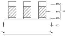
도 3a를 참조하면, 반도체 기판(100) 상에 게이트 절연막(112), 게이트 도전막(114), 그리고 하드 마스크 패턴(116a)을 순차적으로 형성한다.Referring to FIG. 3A, a
상기 반도체 기판(100)은 단결정의 벌크 실리콘 기판일 수 있다. 예컨대, 상기 반도체 기판(100)은 붕소(B)와 같은 피(p)형 불순물이 주입된 피형 반도체 기판일 수 있다.The
상기 게이트 절연막(112)을 형성하는 공정은 열산화 공정 또는 화학적 기상증착(CVD) 공정을 포함할 수 있다. 상기 게이트 절연막(112)은 실리콘 산화막, 하프늄산화막, 하프늄실리케이트막, 지르코늄산화막, 지르코늄실리케이트막, 알루미늄산화막, 그리고 알루미늄실리케이트막 중 어느 하나의 재질로 형성될 수 있다.The step of forming the
상기 게이트 도전막(114)을 형성하는 단계는 화학적 기상증착(CVD) 공정을 포함할 수 있다. 상기 게이트 도전막(114)은 다결정 실리콘 등으로 형성될 수 있다. 이때, 상기 게이트 도전막(114)의 두께는 후속 공정에서 형성되는 게이트 전극의 두께를 고려하여 조절될 수 있다.The step of forming the gate
상기 하드 마스크 패턴(116a)을 형성하는 단계는 상기 게이트 도전막(114) 상에 하드마스크막 및 포토레지스트막을 순차적으로 형성하는 단계, 그리고 상기 포토레지스트막을 마스크로 상기 하드 마스크막을 패터닝하는 단계를 포함할 수 있다. 상기 하드 마스크 패턴(116a)은 상기 게이트 절연막(112) 및 상기 게이트 도전막(114), 그리고 후술할 절연막(120)에 대해 식각 선택성을 가질 수 있는 물질들 중 하나로 형성될 수 있다. 예컨대, 상기 하드 마스크 패턴(116a)은 실리콘질화막 및 실리콘산화질화막 중 적어도 어느 하나를 포함할 수 있다.The step of forming the
그리고, 상기 하드 마스크 패턴(116a)은 상기 게이트 절연막(112) 및 상기 게이트 도전막(114)을 패턴하기 위한 패터닝 공정에서 식각 마스크로 사용될 수 있 다. 이에 더하여, 상기 하드 마스크 패턴(116a)은 후속 공정에서 상기 반도체 기판(100) 전면에 절연막(120)을 형성한 후 평탄화 식각 공정을 진행할 때 식각 저지막으로 사용될 수 있다.The
여기서, 상기 하드 마스크 패턴(116a)의 두께는 후술할 트렌치(trench)(T)의 깊이를 결정하므로, 상기 하드 마스크 패턴(116a)의 두께는 트렌치(T)를 형성하는 후속 공정을 고려하여 조절될 수 있다. 이에 더하여, 상기 하드 마스크 패턴(116a)의 두께는 보이드(V)의 노출을 방지하기 위해 조절될 수 있다. 상기 하드 마스크 패턴(116a)의 두께를 조절하여 보이드(V)의 노출을 방지하는 과정은 후술된다.Since the thickness of the
도 3b를 참조하면, 상기 하드 마스크 패턴(116a)을 마스크로 사용하는 패터닝 공정을 실시하여 게이트 구조물들(110)을 형성한다. 그리고, 상기 게이트 구조물들(110)이 형성된 결과물 전면에 절연막(120)을 형성한다.Referring to FIG. 3B, the
상기 게이트 구조물(110)들을 형성하는 공정은 상기 하드 마스크 패턴(116a)을 식각 마스크로 사용하여 상기 게이트 도전막(114) 및 게이트 절연막(112)을 패터닝함으로써, 상기 반도체 기판(100) 상에 게이트 절연 패턴(112a) 및 게이트 도전 패턴(114a)을 형성하는 단계를 포함할 수 있다. 일 실시예에 따르면, 상기 게이트 도전 패턴(114a)은 부유 게이트 전극패턴, 게이트 층간 절연막, 그리고 컨트롤 게이트 전극을 포함할 수 있다.The
상기 절연막(120)은 상기 마스크 패턴(116a)과 식각 선택성을 가지는 막(예들 들면, 산화막)일 수 있다. 상기 절연막(120)을 형성하는 단계는 화학적 기상증착(CVD) 공정을 사용하는 단계를 포함할 수 있다.The insulating
한편, 상기 보이드(V)의 형성 여부는 상기 절연막(120)을 형성하는 방법 및 상기 게이트 구조물들(110) 사이의 종횡비(aspect ratio) 등에 의해 결정될 수 있다. 예를 들면, 저압 화학적 기상증착(LP-CVD) 공정 또는 물리적 기상증착(PVD) 공정 등과 같이, 단차 도포성(step coverage)이 불량한 증착 기술을 사용하여 절연막(120)을 형성하는 경우에는 알려진 것처럼 게이트 구조물들(110) 사이에 보이드(V)가 생성될 수 있다. 또한, 상기 종횡비가 큰 경우, 상기 절연막(120)이 게이트 구조물들(110) 사이 공간을 완전하게 채우기 어려우므로, 상기 게이트 구조물들(110) 사이에는 보이드(V)가 생성될 가능성이 증가한다. 이때, 상기 종횡비는 게이트 구조물(110)의 높이(h)와 인접한 게이트 구조물들(110) 사이의 간격(w)의 비율(h/w)로 정의될 수 있다.The formation of the voids V may be determined by the method of forming the insulating
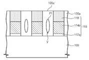
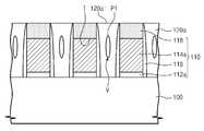
상기와 같은 이유로 형성되는 보이드(V)는 통상적으로 상기 게이트 구조물들(110) 사이에서 상기 절연막(120)에 의해 둘러싸여 노출되지 않는다. 예를 들면, 상기 게이트 구조물들(110)이 형성된 결과물 상에 상기 절연막(120)을 형성하는 경우, 상기 절연막(120)은 서로 인접하는 게이트 구조물들(110)의 사이의 게이트 구조물들(110)의 상부면보다 낮은 위치에서 오버행(overhang)을 형성할 수 있다. 즉, 상기 절연막(120) 형성시 게이트 구조물들(110) 중 어느 하나의 게이트 구조물을 덮는 상기 절연막(120)의 일 부분은 상기 어느 하나의 게이트 구조물과 인접하는 다른 게이트 구조물을 덮는 상기 절연막(120)의 다른 부분과 상기 하드 마스크 패턴(116a)의 상부면보다 낮은 위치에서 연결되는 연결점(connecting point)(P1)을 형성한다. 따라서, 상기 보이드(V)는 통상적으로 상기 게이트 구조물들(110) 사이 에서 상기 절연막(120)에 의해 완전히 매립되어 비노출된 상태로 형성될 수 있다.The voids V formed for the above reasons are not normally surrounded by the insulating
도 3c를 참조하면, 상기 절연막(120)을 식각하여 상기 하드 마스크 패턴(116a)의 상부면(116a')을 노출시키는 절연막 패턴(120a)을 형성한다. 이때, 형성된 상기 절연막 패턴(120a)은 인접한 상기 게이트 구조물들(110) 사이에 배치될 수 있다. 상기 절연막(120)을 식각하는 공정은 상기 하드 마스크 패턴(116a)에 대해 식각 선택성을 갖는 식각 레서피를 사용하는 평탄화 식각 공정을 포함할 수 있다. 그 결과, 상기 절연막 패턴(120a)의 상부면(120a')과 상기 하드 마스크 패턴(116a)의 상부면(116a')은 실질적으로 동일한 높이를 가질 수 있다. 상기 평탄화 식각 공정은 전면 식각(etch-back) 공정 또는 화학적 기계적 연마(CMP) 공정을 포함할 수 있다.Referring to FIG. 3C, the insulating
한편, 상기 평탄화 식각 공정으로 인해 상기 게이트 구조물들(110) 사이에 형성된 보이드(V)가 노출되는 경우에는 앞서 종래 기술에서 설명한 스트링거(stringer) 문제가 발생할 수 있다. 그러나, 본 발명에 따르면, 상기 평탄화 식각 공정은 상기 하드 마스크 패턴(116a)을 식각 저지막으로 사용하므로, 상기 보이드(V)가 노출되는 것을 방지할 수 있다. 즉, 앞서 설명한 바와 같이 상기 보이드(V)는 상기 하드 마스크 패턴(116a)의 상부면(116a')보다 낮은 위치에 형성된다. 따라서, 상기 절연막 패턴(120a)의 상부면(120a')과 상기 하드 마스크 패턴(116a)의 상부면(116a')이 동일한 경우에는 상기 평탄화 식각 공정을 수행하여도 상기 하드 마스크 패턴(116a)의 상부면(116a) 높이에서 상기 평탄화 식각 공정이 중단되므로, 상기 절연막 패턴(120a) 내부에 형성된 상기 보이드(V)의 노출을 방지할 수 있 다.On the other hand, when the voids V formed between the
도 3d를 참조하면, 노출된 상기 하드 마스크 패턴(116a)을 선택적으로 제거하여, 상기 게이트 도전 패턴(114a)의 상부면(114a')을 노출시키는 트렌치(Trench)(T)를 형성한다. 상기 하드 마스크 패턴(116a)을 제거하는 단계는 상기 하드 마스크 패턴(116a)의 식각 속도에 비해 상기 절연막 패턴(120a)와 상기 게이트 도전 패턴(114a)의 식각 속도가 느린 식각 레서피를 사용하여 상기 하드 마스크 패턴(116a)을 선택적으로 식각하는 단계를 포함할 수 있다. 이러한 식각 단계는 습식 또는 건식 식각 등의 방법으로 실시될 수 있다.Referring to FIG. 3D, the exposed
도 3e를 참조하면, 상기 트렌치(T)가 형성된 결과물에 금속막(130) 및 산화방지막(150)을 순차적으로 형성한다.Referring to FIG. 3E, a
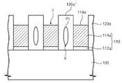
상기 금속막(130)은 트렌치(T)가 형성된 결과물을 콘포멀하게 덮도록 형성될 수 있다. 이를 위해, 상기 금속막(130)은 화학적 기상증착(CVD) 공정 또는 무전해 증착 공정 등을 사용하여 형성될 수 있다. 또는, 다른 실시예로서, 상기 금속막(130)은 물리적 기상증착 공정을 사용하여 형성될 수도 있다. 여기서, 상기 금속막(130)의 두께(t)는 상기 트렌치(T)의 폭(w)의 절반보다 얇게 형성될 수 있다. 이는 후속 공정으로 상기 산화방지막(150)을 형성할 때, 상기 트렌치(T) 내부에 상기 산화방지막(150)이 효과적으로 매립되도록 하기 위함이다. 상기 금속막(130)은 다결정 실리콘으로 이루어진 상기 게이트 도전 패턴(114a)과 반응하여 실리사이드 화합물을 형성할 수 있는 물질들 중 적어도 하나일 수 있다. 예를 들면, 상기 금속막(130)은 코발트(Co), 니켈(Ni), 탄탈늄(Ta), 텅스텐(W), 그리고 몰리브덴(Mo) 중 적어도 어느 하나를 포함할 수 있다.The
상기 산화방지막(150)은 상기 금속막(130)이 형성된 결과물 전면을 덮도록 형성될 수 있다. 이때, 상기 산화방지막(150)은 도시된 것처럼, 상기 금속막(130)에 의해 채워지지 않는 상기 트렌치(T) 내 공간을 완전히 채우도록 형성될 수 있다. 상기 산화방지막(150)을 형성하는 단계는 화학적 기상증착(CVD) 공정 또는 물리적 기상 증착 공정 등을 사용하여 형성될 수 있다. 상기 산화방지막(150)은 상기 금속막(130)의 산화를 방지할 수 있는 물질들 중 어느 하나일 수 있다. 예를 들면, 상기 산화방지막(150)은 티타늄질화물(TiN), 티타늄텅스텐(TiW), 그리고 실리콘 질화막 중 적어도 어느 하나일 수 있다.The
한편, 상기 금속막(130)의 두께는 얇게 형성될 수 있다. 일반적으로 상기 금속막(130)이 코발트(Co)인 경우에는 코발트(Co)의 두께의 대략 3.2 내지 4.0배에 해당되는 실리사이드가 형성될 수 있다. 따라서, 코발트(Co)의 두께가 증가하면, 실리사이드막으로 바뀌는 상기 게이트 도전 패턴(114a)의 영역이 증가하므로, 상기 트렌치(T) 상에 형성되는 상기 금속막(130)의 두께(t)를 얇게하여 실리사이드화 공정시 실리사이드막으로 바뀌는 상기 게이트 도전 패턴(114a)의 영역을 감소시킬 수 있다.On the other hand, the thickness of the
도 3f를 참조하면, 실리사이드화 공정을 실시하여, 상기 금속막(130)과 상기 게이트 도전 패턴(114a)을 반응시킴으로써, 상기 게이트 도전 패턴(114a)의 상부에 실리사이드막(118)을 형성한다. 상기 실리사이드화 공정은 급속열처리(RTA:Rapid Thermal Anneal) 공정 또는 가열로 열처리(Furnace anneal) 공정을 포함할 수 있 다. 상기 실리사이드막(118)은 코발트실리사이드(CoSi2), 니켈실리사이드(NiSi2), 탄탈늄실리사이드(TaSi2), 텅스텐실리사이드(WSi2), 그리고 몰리브덴실리사이드(MoSi2)들 중 어느 하나일 수 있다.Referring to FIG. 3F, a
도 3g를 참조하면, 상기 실리사이드막(118) 형성 공정이 완료되면, 미반응된 금속막(130) 및 상기 산화방지막(150)을 제거한다. 상기 미반응된 금속막(130) 및 상기 산화방지막(150) 제거 공정은 습식 식각 공정, 화학기계적 연마 공정, 그리고 에치백 공정 등을 포함할 수 있다. 그리고, 후속 공정을 위해, 상기 미반응된 금속막(130) 및 상기 산화방지막(150) 제거 공정이 수행된 결과물 상에 층간 절연막(160)을 형성할 수도 있다.Referring to FIG. 3G, when the
상술한 바와 같이, 본 발명의 일 실시예에 따르면, 상기 절연막(120)을 형성하는 공정을 수행할 때 상기 게이트 구조물들(110) 사이에 상기 보이드(V)가 형성되더라도, 상기 실리사이드화 공정을 실시할 때까지 상기 보이드(V)가 노출되지 않으므로, 상기 보이드(V)에 상기 금속막(130)이 유입됨으로써 발생되는 스트링거 현상을 방지할 수 있다.As described above, according to an embodiment of the present invention, even if the voids V are formed between the
(실시예2)(Example 2)
도 4a 내지 도 4e는 본 발명의 다른 실시예에 따른 반도체 소자 제조 방법을 설명하기 위한 도면들이다. 여기서, 본 실시예는 상술한 상기 실시예1과 상이한 점을 중심으로 설명하며, 상기 실시예1과 동일한 내용에 대해서는 개략적으로 설명하거나 생략한다.4A to 4E are views for explaining a method of manufacturing a semiconductor device according to another embodiment of the present invention. Here, the present embodiment will be described mainly focusing on the differences from the above-described first embodiment, and the same contents as those of the first embodiment will be schematically explained or omitted.
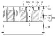
도 4a를 참조하면, 상기 도 3d를 참조하여 설명된 구조물에 금속막(130) 및 실리콘막(140)을 순차적으로 형성한다. 상기 금속막(130)을 형성하는 단계는 실시예1에서 설명한 방법과 동일하게 수행될 수 있다. 이때, 상기 금속막(130)의 두께(t)는 상기 트렌치(T)의 폭(w)의 절반보다 얇게 형성될 수 있다. 이는 상기 실리콘막(140)이 상기 트렌치(T) 내부에 효과적으로 매립되도록 하기 위함이다.Referring to FIG. 4A, a
상기 실리콘막(140)을 형성하는 단계는 상기 금속막(130)이 형성된 결과물의 전면을 덮도록 형성될 수 있다. 상기 실리콘막(140)은 상기 금속막(130)과 반응하여 실리사이드 화합물을 형성할 수 있는 물질을 포함할 수 있다. 상기 실리콘막(140)은 도시된 것처럼, 상기 금속막(130)에 의해 채워지지 않는 상기 트렌치(T) 내 공간을 완전히 채우도록 형성될 수 있다. 또는, 다른 실시예로서, 실리콘막(140)은 상기 트렌치(T)가 형성된 결과물 전면에 콘포멀하게 형성될 수도 있다. 상기 실리콘막(140)은 화학적 기상증착(CVD) 공정을 사용하여 형성될 수 있다. 또는, 다른 실시예로서 상기 실리콘막(140)은 물리적 기상증착(PVD) 공정 등을 사용하여 형성될 수 있다.The step of forming the
도 4b를 참조하면, 상기 실리콘막(140)이 형성된 결과물을 식각하여 상기 절연막 패턴(120a)을 노출시킨다. 상기 실리콘막(140)을 식각하는 공정은 상기 절연막 패턴(120a)을 식각 저지막으로 사용하는 평탄화 식각 공정을 포함할 수 있다. 이러한 평탄화 식각 공정은 화학기계적 연마 공정 및 에치백 공정 등을 포함할 수 있다. 그 결과, 트렌치(T) 내 공간에 형성된 실리콘막(140a)의 상부면(140a')은 상기 절연막 패턴(120a)의 상부면(120a')의 높이와 동일할 수 있다.Referring to FIG. 4B, the insulating
도 4c 및 도 4d를 참조하면, 상기 절연막 패턴(120a)이 노출된 결과물 전면에 산화방지막(150)을 형성한다. 상기 산화방지막(150)은 상기 절연막 패턴(120a)이 노출된 결과물을 콘포멀하게 덮도록 형성될 수 있다. 상기 산화방지막(150)은 화학적 기상증착(CVD) 공정을 사용하여 형성될 수 있다. 또는, 상기 산화방지막(150)은 무전해 증착 공정 또는 물리적 기상증착(PVD) 공정 등을 사용하여 형성될 수 있다. 상기 산화방지막(150)은 티타늄질화물(TiN), 티타늄텅스텐(TiW), 그리고 실리콘 질화막 중 적어도 어느 하나일 수 있다.Referring to FIGS. 4C and 4D, the
상기 산화방지막(150)이 형성된 결과물 상에 실리사이드화 공정을 수행하여, 상기 게이트 도전 패턴(114a)의 상부에 실리사이드막(118)을 형성한다. 여기서, 상기 실리사이드화 공정은 상기 금속막(130)을 상기 게이드 도전 패턴(114a) 및 상기 실리콘막(150)과 동시에 반응시켜, 상기 게이드 도전패턴(114a)의 상부에 상기 실리사이드막(118)을 형성한다. 즉, 상기 실리사이드화 공정시 상기 트렌치(T)의 하부면과 접촉되는 금속막(130)은 상기 게이트 도전 패턴(114a) 및 상기 실리콘막(150)과 동시에 실리사이드화 반응한다. 따라서, 본 실시예에 따른 상기 실리사이드화 공정은 실시예1과 같이 상기 금속막(130)이 상기 게이트 도전 패턴(114a)하고만 상기 실리사이드화 반응이 수행되는 경우에 비해, 상기 실리사이드막(118)으로 바뀌는 상기 게이트 도전 패턴(114a)의 영역을 감소시킬 수 있다.A silicidation process is performed on the resultant product in which the
한편, 앞서 설명한 바와 같이, 일반적으로 상기 금속막(130)이 코발트(Co)인 경우에는 코발트(Co)의 두께의 대략 3.2 내지 4.0배에 해당되는 실리사이드가 형성될 수 있으므로, 상기 금속막(130)의 두께(t)는 이를 고려하여 조절될 수 있다. 예 를 들면, 상기 금속막(130)의 두께(t)(특히, 게이트 도전 패턴(114a)의 상부면(114a') 상에 형성되는 금속막(130)의 두께)는 상기 트렌치(T)의 폭(w)의 1/8 내지 1/6의 두께로 형성될 수 있다. 바람직하게는 상기 금속막(130)의 두께(t)는 상기 트렌치(T)의 폭(w)의 1/7.2의 두께로 형성될 수 있다.As described above, generally, when the
도 4e를 참조하면, 상기 실리사이드막(118) 형성 공정이 완료되면, 산화방지막(150)을 제거하는 공정이 수행된다. 상기 산화방지막(150) 제거 공정은 습식 식각 공정, 화학기계적 연마 공정, 그리고 에치백 공정 등을 포함할 수 있다.Referring to FIG. 4E, when the
상술한 바와 같이, 본 발명의 다른 실시예에 따른 반도체 소자 제조 방법은 상술한 실시예1에 비해, 실리사이드막(118)으로 바뀌는 상기 게이트 도전 패턴(114a)의 영역을 감소시킬 수 있다.As described above, the method for fabricating a semiconductor device according to another embodiment of the present invention can reduce the area of the gate
또한, 본 실시예의 다른 실시예에 따른 반도체 소자 제조 방법은 상술한 실시예1에 비해, 상기 트렌치(T)에 상기 실리콘막(140)을 형성한 후 상기 절연막(120)을 식각 저지막으로 사용하는 평탄화 공정을 더 포함함으로써, 콘포멀한 산화방지막(150)을 형성할 수 있다.The method of manufacturing a semiconductor device according to another embodiment of the present invention is different from the first embodiment in that the
(실시예3)(Example 3)
도 5a 내지 도 5i는 본 발명의 또 다른 실시예에 따른 반도체 소자 제조 방법을 설명하기 위한 도면들이다. 여기서, 본 실시예는 상술한 실시예1 및 실시예2와 상이한 점을 중심으로 설명하며, 상술한 실시예1 및 실시예2와 동일한 내용에 대해서는 개략적으로 설명하거나 생략한다.5A to 5I are views for explaining a method of manufacturing a semiconductor device according to another embodiment of the present invention. Here, the present embodiment will be described mainly focusing on the points different from the above-described first and second embodiments, and the same contents as those of the above-described first and second embodiments will be schematically explained or omitted.
도 5a 및 도 5b를 참조하면, 상기 도 3a를 참조하여 설명된 구조물의 상기 하드 마스크 패턴(116a)을 마스크로 사용하는 패터닝 공정을 실시하여 상기 게이트 구조물들(110)을 형성한다. 이때, 상기 게이트 구조물들(110)을 형성하는 공정은 상술한 실시예1 및 실시예2에서 설명한 게이트 구조물들(110) 형성 공정들에 비해 스페이서(119)를 형성하는 공정을 더 포함한다. 상기 스페이서(119)는 게이트 절연 패턴(112a), 게이트 도전 패턴(114a), 그리고 하드 마스크 패턴(116a)이 형성된 결과물 전면에 콘포멀하게 스페이서 형성을 위한 막을 형성한 후 전면 이방성 식각 공정을 수행하여 형성될 수 있다. 상기 스페이서(119)는 실리콘산화막일 수 있다.5A and 5B, the
여기서, 본 실시예에서는 게이트 구조물들(110) 사이의 반도체 기판(100) 영역에 불순물 영역(미도시됨)을 형성시키는 공정을 더 포함할 수 있다. 예컨대, 게이트 구조물들(110)이 형성된 반도체 기판(100)에 대해 불순물 주입 공정을 수행하여, 게이트 구조물들(110) 사이의 반도체 기판(100) 영역에 불순물 영역을 형성한다. 상기 불순물 영역은 소오스/드레인 영역일 수 있다. 상기 소오스/드레인 영역은 저농도 소오스/드레인 영역 및 고농도 소오스/드레인 영역을 포함할 수 있다.Here, in this embodiment, a process of forming an impurity region (not shown) in the region of the
도 5c 및 도 5d를 참조하면, 게이트 구조물(110)들 각각의 측부에 스페이서(119)가 형성된 결과물 상에 절연막(120)을 형성한다. 상기 절연막(120)은 산화막일 수 있다. 그리고, 절연막(120)이 형성된 결과물을 식각하는 평탄화 식각공정을 통해 하드 마스크 패턴(116a)의 상부면(116a')을 노출시킨다.5C and 5D, an insulating
도 5e를 참조하면, 상기 노출된 하드 마스크 패턴(116a)을 선택적으로 제거하여, 상기 게이드 도전패턴(114a)의 상부면(114a')을 노출시키는 트렌치(T)를 형 성한다. 상기 트렌치(T)를 형성하는 단계는 상기 하드 마스크 패턴(116a)에 대해 식각 선택성을 갖는 식각 레서피를 사용하는 식각 공정을 포함할 수 있다. 상기 하드 마스크 패턴(116a)을 식각하는 공정은 등방성 습식 식각 공정을 포함할 수 있다. 여기서, 상기 하드 마스크 패턴(116a)을 식각하는 공정은 상기 하드 마스크 패턴(116a) 제거시 상기 스페이서(119)가 손상되지 않도록 상기 하드 마스크 패턴(116a)에 대해 우수한 식각 선택성을 가지는 공정을 사용할 수 있다.Referring to FIG. 5E, the exposed
도 5f를 참조하면, 상기 트렌치(T)가 형성된 결과물에 금속막(130) 및 실리콘막(140)을 순차적으로 형성한다. 상기 금속막(130) 및 상기 실리콘막(140)을 형성하는 단계는 상술한 실시예2의 상기 금속막(130) 형성 공정 및 상기 실리콘막(140) 형성 공정과 동일한 방법으로 진행될 수 있다.Referring to FIG. 5F, a
도 5g를 참조하면, 상기 실리콘막(140)이 형성된 결과물을 식각하여 상기 절연막 패턴(120a)을 노출시킨다. 그리고, 상기 절연막 패턴(120a)이 노출된 결과물 전면에 산화방지막(150)을 형성한다.Referring to FIG. 5G, the insulating
상기 실리콘막(140)을 식각하는 공정은 상기 절연막 패턴(120a)을 식각 저지막으로 사용하는 평탄화 식각 공정을 포함할 수 있다. 그 결과, 트렌치(T) 내 공간에 형성된 실리콘막(140a)의 상부면은 상기 절연막 패턴(120a)의 상부면(120a')의 높이와 동일할 수 있다.The step of etching the
상기 산화방지막(150)은 상기 절연막 패턴(120a)이 노출된 결과물을 콘포멀하게 덮도록 형성될 수 있다. 상기 산화방지막(150)은 화학적 기상증착(CVD) 공정 또는 무전해 증착 공정 등을 사용하여 형성될 수 있다.The
도 5h 및 도 5i를 참조하면, 상기 산화방지막(150)이 형성된 결과물 상에 실리사이드화 공정을 수행하여, 상기 게이트 도전 패턴(114a)의 상부에 실리사이드막(118)을 형성한 후 산화방지막(150)을 제거한다.5H and 5I, a silicidation process is performed on the resultant product having the
상술한 본 발명의 또 다른 실시예에 따른 반도체 소자 제조 방법은 상술한 실시예1 및 실시예2에 비해 스페이서(119)를 구비하는 게이트 구조물들(110)을 형성할 수 있다.The method of fabricating a semiconductor device according to another embodiment of the present invention described above can form the
도 6은 본 발명에 따른 반도체 소자를 구비하는 메모리 카드의 일 예를 간략히 도시한 블록도이다. 상기 반도체 소자는 플래시 메모리 장치일 수 있다. 도 6을 참조하면, 고용량의 데이터 저장 능력을 지원하기 위한 메모리 카드(200)는 본 발명에 따른 플래시 메모리 장치(210)를 장착한다. 본 발명에 따른 메모리 카드(200)는 호스트(Host)와 플래시 메모리 장치(210) 간의 제반 데이터 교환을 제어하는 메모리 컨트롤러(220)를 포함한다.6 is a block diagram briefly showing an example of a memory card having a semiconductor device according to the present invention. The semiconductor device may be a flash memory device. Referring to FIG. 6, a
프로세싱 유닛(222)의 동작 메모리로써 SRAM(221)이 사용될 수 있다. 호스트 인터페이스(223)는 메모리 카드(200)와 접속되는 호스트의 데이터 교환 프로토콜을 구비한다. 에러 정정 블록(224)은 멀티 비트 플래시 메모리 장치(210)로부터 독출된 데이터에 포함되는 에러를 검출 및 정정한다. 메모리 인터페이스(225)는 본 발명의 플래시 메모리 장치(210)와 인터페이싱 한다. 프로세싱 유닛(222)은 메모리 컨트롤러(220)의 데이터 교환을 위한 제반 제어 동작을 수행한다. 비록 도면에는 도시되지 않았지만, 본 발명에 따른 메모리 카드(200)는 호스트(Host)와의 인터페 이싱을 위한 코드 데이터를 저장하는 ROM(미도시됨) 등이 더 제공될 수 있음은 이 분야의 통상적인 지식을 습득한 자들에게 자명하다. 특히, 반도체 디스크 장치(Solid State Disk:이하 SSD) 장치와 같은 메모리 시스템에서 본 발명의 플래시 메모리 장치가 제공될 수 있다.The
도 7은 본 발명에 따른 반도체 소자를 장착하는 정보 처리 시스템을 간략히 보여주는 블록도이다. 상기 반도체 소자는 플래시 메모리 시스템(310)일 수 있다. 도 7을 참조하면, 모바일 기기나 데스크 톱 컴퓨터와 같은 정보 처리 시스템에 본 발명의 플래시 메모리 시스템(310)이 장착될 수 있다. 플래시 메모리 시스템(310)은 앞서 도 1 내지 도 5i를 참조하여 설명한 본 발명의 기술적 특징을 포함하는 플래시 메모리 장치(311) 및 상기 플래시 메모리 장치(311)를 제어하는 메모리 컨트롤러(312)를 포함할 수 있다.7 is a block diagram briefly showing an information processing system for mounting a semiconductor device according to the present invention. The semiconductor device may be a
본 발명에 따른 정보 처리 시스템(300)은 플래시 메모리 시스템(310) 및 각각 시스템 버스(360)에 전기적으로 연결된 모뎀(320), 중앙처리장치(330), 램(340), 유저 인터페이스(350)를 포함할 수 있다. 플래시 메모리 시스템(310)은 앞서 언급된 플래시 메모리 장치와 실질적으로 동일하게 구성될 것이다. 플래시 메모리 시스템(310)에는 중앙처리장치(330)에 의해서 처리된 데이터 또는 외부에서 입력된 데이터가 저장될 수 있다. 여기서, 상술한 플래시 메모리 시스템(310)이 반도체 디스크 장치(SSD)로 구성될 수 있으며, 이 경우 정보 처리 시스템(300)은 대용량의 데이터를 플래시 메모리 시스템(310)에 안정적으로 저장할 수 있다. 그리고 신뢰성의 증대에 따라, 플래시 메모리 시스템(310)은 에러 정정에 소요되는 자원을 절감할 수 있어 고속의 데이터 교환 기능을 정보 처리 시스템(300)에 제공할 것이다. 도시되지 않았지만, 본 발명에 따른 정보 처리 시스템(300)에는 응용 칩셋(Application Chipset), 카메라 이미지 프로세서(Camera Image Processor:CIS), 입출력 장치 등이 더 제공될 수 있음은 이 분야의 통상적인 지식을 습득한 자들에게 자명하다.The
또한, 본 발명에 따른 반도체 소자는 다양한 형태들의 패키지로 실장 될 수 있다. 예를 들면, 본 발명에 따른 반도체 소자(예컨대, 플래시 메모리 장치 또는 메모리 시스템)은 PoP(Package on Package), Ball grid arrays(BGAs), Chip scale packages(CSPs), Plastic Leaded Chip Carrier(PLCC), Plastic Dual In-Line Package(PDIP), Die in Waffle Pack, Die in Wafer Form, Chip On Board(COB), Ceramic Dual In-Line Package(CERDIP), Plastic Metric Quad Flat Pack(MQFP), Thin Quad Flatpack(TQFP), Small Outline(SOIC), Shrink Small Outline Package(SSOP), Thin Small Outline(TSOP), Thin Quad Flatpack(TQFP), System In Package(SIP), Multi Chip Package(MCP), Wafer-level Fabricated Package(WFP), Wafer-Level Processed Stack Package(WSP) 등과 같은 방식으로 패키지화되어 설치될 수 있다.Further, the semiconductor device according to the present invention can be mounted in various types of packages. For example, a semiconductor device (e.g., a flash memory device or a memory system) according to the present invention may be implemented as a package on package (PoP), ball grid arrays (BGAs), chip scale packages (CSPs), plastic leaded chip carriers Plastic In-Line Package (PDIP), Die in Waffle Pack, Die in Wafer Form, Chip On Board (COB), Ceramic Dual In-Line Package (CERDIP), Plastic Metric Quad Flat Pack (MQFP) TQFP), Small Outline (SOIC), Shrink Small Outline Package (SSOP), Thin Small Outline (TSOP), Thin Quad Flatpack (TQFP), System In Package (SIP), Multi Chip Package (WFP), a Wafer-Level Processed Stack Package (WSP), and the like.
한편, 소오스/드레인 전극을 게이트 전압을 이용하여 형성하는 기술을 개시하는 "semiconductor Device Having A Field Effect Source/Drain Region"라는 제목의 미국공개특허번호 US 2007/0205445 및 절연성 기판 상에 3차원적으로 비휘발 성 메모리 셀들을 형성하는 기술을 개시하는 "thin Film Transistor With Metal Oxide Layer And Method Of Making Same"라는 제목의 미국특허번호 US 6,858,899 에서 설명되는 발명들은 상술한 본 발명의 기술적 특징들과 결합되어 본 발명의 또다른 실시예들을 구성할 수 있다. 이에 더하여, "non-Volatile Semiconductor Memory Devices"라는 제목의 미국특허번호 US 7,253,467, "non-Volatile Memory Devices And Methods Of Operating The Same"라는 제목의 미국공개특허번호 US 2006/0180851, "nonvolatile Semiconductor Memory"라는 제목의 미국특허번호 US 5,473,563 및 "memory Devices With Page Buffer Having Dual Legisters And Method Of Using The Same"라는 제목의 미국특허번호 US 7,042,770에서 설명되는 발명들 역시 상술한 본 발명의 기술적 특징들과 결합되어 본 발명의 또 다른 실시예들을 구성할 수 있다.On the other hand, US Patent Application No. US 2007/0205445 entitled " semiconductor Device Having A Field Source / Drain Region ", which discloses a technique for forming a source / drain electrode using a gate voltage, The invention described in U.S. Patent No. 6,858,899 entitled " Thin Film Transistor With Metal Oxide Layer And Method Of Making Same ", which discloses a technique for forming nonvolatile memory cells, is combined with the technical features of the present invention described above Other embodiments of the present invention may be configured. In addition, U.S. Patent No. 7,253,467 entitled "Non-Volatile Semiconductor Memory Devices", U.S. Published Patent Application No. 2006/0180851 entitled "Non-Volatile Memory Devices and Methods of Operating The Same" And US Patent No. 7,042,770 entitled " Memory Devices With Dual Legisces And Method Of Using The Same ", also incorporated herein by reference in its entirety, Other embodiments of the present invention may be configured.
이상의 상세한 설명은 본 발명을 예시하는 것이다. 또한 전술한 내용은 본 발명의 바람직한 실시 형태를 나타내고 설명하는 것에 불과하며, 본 발명은 다양한 다른 조합, 변경 및 환경에서 사용할 수 있다. 즉, 본 명세서에 개시된 발명의 개념의 범위, 저술한 개시 내용과 균등한 범위 및/또는 당업계의 기술 또는 지식의 범위 내에서 변경 또는 수정이 가능하다. 전술한 실시예들은 본 발명을 실시하는데 있어 최선의 상태를 설명하기 위한 것이며, 본 발명과 같은 다른 발명을 이용하는데 당업계에 알려진 다른 상태로의 실시, 그리고 발명의 구체적인 적용 분야 및 용도에서 요구되는 다양한 변경도 가능하다. 따라서, 이상의 발명의 상세한 설명은 개시된 실시 상태로 본 발명을 제한하려는 의도가 아니다. 또한 첨부된 청구범위는 다른 실시 상태도 포함하는 것으로 해석되어야 한다.The foregoing detailed description is illustrative of the present invention. It is also to be understood that the foregoing is illustrative and explanatory of preferred embodiments of the invention only, and that the invention may be used in various other combinations, modifications and environments. That is, it is possible to make changes or modifications within the scope of the concept of the invention disclosed in this specification, the disclosure and the equivalents of the disclosure and / or the scope of the art or knowledge of the present invention. The foregoing embodiments are intended to illustrate the best mode contemplated for carrying out the invention and are not intended to limit the scope of the present invention to other modes of operation known in the art for utilizing other inventions such as the present invention, Various changes are possible. Accordingly, the foregoing description of the invention is not intended to limit the invention to the precise embodiments disclosed. It is also to be understood that the appended claims are intended to cover such other embodiments.
도 1은 본 발명에 따른 반도체 소자의 셀 어레이를 도시하는 회로도이다.1 is a circuit diagram showing a cell array of semiconductor devices according to the present invention.
도 2는 본 발명에 따른 반도체 소자의 구성을 개략적으로 설명하기 위한 블록도이다.2 is a block diagram schematically illustrating a configuration of a semiconductor device according to the present invention.
도 3a 내지 도 3g는 본 발명의 일 실시예에 따른 반도체 소자 제조 방법을 설명하기 위한 도면들이다.3A to 3G are views for explaining a method of manufacturing a semiconductor device according to an embodiment of the present invention.
도 4a 내지 도 4e는 본 발명의 다른 실시예에 따른 반도체 소자 제조 방법을 설명하기 위한 도면들이다.4A to 4E are views for explaining a method of manufacturing a semiconductor device according to another embodiment of the present invention.
도 5a 내지 도 5i는 본 발명의 또 다른 실시예에 따른 반도체 소자 제조 방법을 설명하기 위한 도면들이다.5A to 5I are views for explaining a method of manufacturing a semiconductor device according to another embodiment of the present invention.
도 6은 본 발명에 따른 반도체 소자를 구비하는 메모리 카드의 일 예를 간략히 도시한 블록도이다.6 is a block diagram briefly showing an example of a memory card having a semiconductor device according to the present invention.
도 7은 본 발명에 따른 반도체 소자를 장착하는 정보 처리 시스템을 간략히 보여주는 블록도이다.7 is a block diagram briefly showing an information processing system for mounting a semiconductor device according to the present invention.
*도면의 주요 부분에 대한 부호 설명*Description of the Related Art [0002]
100 : 반도체 기판100: semiconductor substrate
110 : 게이트 구조물110: gate structure
120 : 절연막120: insulating film
130 : 금속막130: metal film
140 : 실리콘막140: silicon film
150 : 산화방지막150: oxidation prevention film
Claims (18)
Translated fromKoreanPriority Applications (2)
| Application Number | Priority Date | Filing Date | Title |
|---|---|---|---|
| KR1020080013988AKR101408782B1 (en) | 2008-02-15 | 2008-02-15 | manufacturing method for semiconductor device |
| US12/379,190US8053347B2 (en) | 2008-02-15 | 2009-02-13 | Method of manufacturing semiconductor device |
Applications Claiming Priority (1)
| Application Number | Priority Date | Filing Date | Title |
|---|---|---|---|
| KR1020080013988AKR101408782B1 (en) | 2008-02-15 | 2008-02-15 | manufacturing method for semiconductor device |
Publications (2)
| Publication Number | Publication Date |
|---|---|
| KR20090088603A KR20090088603A (en) | 2009-08-20 |
| KR101408782B1true KR101408782B1 (en) | 2014-06-19 |
Family
ID=41013508
Family Applications (1)
| Application Number | Title | Priority Date | Filing Date |
|---|---|---|---|
| KR1020080013988AActiveKR101408782B1 (en) | 2008-02-15 | 2008-02-15 | manufacturing method for semiconductor device |
Country Status (2)
| Country | Link |
|---|---|
| US (1) | US8053347B2 (en) |
| KR (1) | KR101408782B1 (en) |
Families Citing this family (19)
| Publication number | Priority date | Publication date | Assignee | Title |
|---|---|---|---|---|
| US8546239B2 (en) | 2010-06-11 | 2013-10-01 | Sandisk Technologies Inc. | Methods of fabricating non-volatile memory with air gaps |
| US8946048B2 (en) | 2010-06-19 | 2015-02-03 | Sandisk Technologies Inc. | Method of fabricating non-volatile memory with flat cell structures and air gap isolation |
| US8603890B2 (en) | 2010-06-19 | 2013-12-10 | Sandisk Technologies Inc. | Air gap isolation in non-volatile memory |
| US8492224B2 (en)* | 2010-06-20 | 2013-07-23 | Sandisk Technologies Inc. | Metal control gate structures and air gap isolation in non-volatile memory |
| KR101559345B1 (en)* | 2010-08-26 | 2015-10-15 | 삼성전자주식회사 | Non volatile memory device and method for manufacturing the same |
| US8778749B2 (en) | 2011-01-12 | 2014-07-15 | Sandisk Technologies Inc. | Air isolation in high density non-volatile memory |
| US9123714B2 (en) | 2012-02-16 | 2015-09-01 | Sandisk Technologies Inc. | Metal layer air gap formation |
| US9123577B2 (en) | 2012-12-12 | 2015-09-01 | Sandisk Technologies Inc. | Air gap isolation in non-volatile memory using sacrificial films |
| US9349740B2 (en) | 2014-01-24 | 2016-05-24 | Sandisk Technologies Inc. | Non-volatile storage element with suspended charge storage region |
| US9177853B1 (en) | 2014-05-14 | 2015-11-03 | Sandisk Technologies Inc. | Barrier layer stack for bit line air gap formation |
| US9478461B2 (en) | 2014-09-24 | 2016-10-25 | Sandisk Technologies Llc | Conductive line structure with openings |
| US9524904B2 (en) | 2014-10-21 | 2016-12-20 | Sandisk Technologies Llc | Early bit line air gap formation |
| US9847249B2 (en) | 2014-11-05 | 2017-12-19 | Sandisk Technologies Llc | Buried etch stop layer for damascene bit line formation |
| US9401305B2 (en) | 2014-11-05 | 2016-07-26 | Sandisk Technologies Llc | Air gaps structures for damascene metal patterning |
| KR102302231B1 (en) | 2015-03-05 | 2021-09-14 | 삼성전자주식회사 | Non volatile memory devices and methods of manufacturing the same |
| US9524973B1 (en) | 2015-06-30 | 2016-12-20 | Sandisk Technologies Llc | Shallow trench air gaps and their formation |
| US9524974B1 (en) | 2015-07-22 | 2016-12-20 | Sandisk Technologies Llc | Alternating sidewall assisted patterning |
| US9607997B1 (en) | 2015-09-08 | 2017-03-28 | Sandisk Technologies Inc. | Metal line with increased inter-metal breakdown voltage |
| US9391081B1 (en) | 2015-09-08 | 2016-07-12 | Sandisk Technologies Llc | Metal indentation to increase inter-metal breakdown voltage |
Citations (4)
| Publication number | Priority date | Publication date | Assignee | Title |
|---|---|---|---|---|
| KR19980068057A (en)* | 1997-02-14 | 1998-10-15 | 김광호 | Trench element isolation |
| US20070040225A1 (en)* | 2005-08-22 | 2007-02-22 | Yang Haining S | High performance MOSFET comprising a stressed gate metal silicide layer and method of fabricating the same |
| KR100706225B1 (en) | 2001-04-20 | 2007-04-11 | 삼성전자주식회사 | Gate insulation structure and its formation method |
| KR100794085B1 (en) | 2006-06-28 | 2008-01-10 | 주식회사 하이닉스반도체 | Manufacturing Method of Flash Memory Device |
Family Cites Families (10)
| Publication number | Priority date | Publication date | Assignee | Title |
|---|---|---|---|---|
| US6015752A (en)* | 1998-06-30 | 2000-01-18 | Advanced Micro Devices, Inc. | Elevated salicide technology |
| US20060180851A1 (en)* | 2001-06-28 | 2006-08-17 | Samsung Electronics Co., Ltd. | Non-volatile memory devices and methods of operating the same |
| US7253467B2 (en)* | 2001-06-28 | 2007-08-07 | Samsung Electronics Co., Ltd. | Non-volatile semiconductor memory devices |
| US7042770B2 (en)* | 2001-07-23 | 2006-05-09 | Samsung Electronics Co., Ltd. | Memory devices with page buffer having dual registers and method of using the same |
| US6858899B2 (en)* | 2002-10-15 | 2005-02-22 | Matrix Semiconductor, Inc. | Thin film transistor with metal oxide layer and method of making same |
| TWI270180B (en)* | 2004-06-21 | 2007-01-01 | Powerchip Semiconductor Corp | Flash memory cell and manufacturing method thereof |
| US7348618B2 (en)* | 2005-03-30 | 2008-03-25 | Intel Corporation | Flash memory cell having reduced floating gate to floating gate coupling |
| KR100673020B1 (en)* | 2005-12-20 | 2007-01-24 | 삼성전자주식회사 | Semiconductor device having field effect source / drain regions |
| JP4868864B2 (en)* | 2006-01-31 | 2012-02-01 | 株式会社東芝 | Manufacturing method of semiconductor device |
| US7642153B2 (en)* | 2007-10-23 | 2010-01-05 | Texas Instruments Incorporated | Methods for forming gate electrodes for integrated circuits |
- 2008
- 2008-02-15KRKR1020080013988Apatent/KR101408782B1/enactiveActive
- 2009
- 2009-02-13USUS12/379,190patent/US8053347B2/enactiveActive
Patent Citations (4)
| Publication number | Priority date | Publication date | Assignee | Title |
|---|---|---|---|---|
| KR19980068057A (en)* | 1997-02-14 | 1998-10-15 | 김광호 | Trench element isolation |
| KR100706225B1 (en) | 2001-04-20 | 2007-04-11 | 삼성전자주식회사 | Gate insulation structure and its formation method |
| US20070040225A1 (en)* | 2005-08-22 | 2007-02-22 | Yang Haining S | High performance MOSFET comprising a stressed gate metal silicide layer and method of fabricating the same |
| KR100794085B1 (en) | 2006-06-28 | 2008-01-10 | 주식회사 하이닉스반도체 | Manufacturing Method of Flash Memory Device |
Also Published As
| Publication number | Publication date |
|---|---|
| US20090221138A1 (en) | 2009-09-03 |
| US8053347B2 (en) | 2011-11-08 |
| KR20090088603A (en) | 2009-08-20 |
Similar Documents
| Publication | Publication Date | Title |
|---|---|---|
| KR101408782B1 (en) | manufacturing method for semiconductor device | |
| US10199390B2 (en) | Nonvolatile memory device and method of manufacturing the same | |
| US10332902B2 (en) | Three-dimensional semiconductor memory device including vertically stacked electrodes | |
| US8120089B2 (en) | Non-volatile memory device and method for fabricating non-volatile memory device | |
| KR102015578B1 (en) | Nonvolatile memory device and manufactureing the same | |
| CN102544017B (en) | Nonvolatile memory and manufacture method thereof | |
| KR101725446B1 (en) | Semiconductor Devices and Methods of Fabricating the Same | |
| KR20160024087A (en) | Semiconductor device, manufacturing method of semiconductor device and method of forming epitaxial layer | |
| KR20150083319A (en) | Nonvolatile memory device and manufactureing the same | |
| US20110275197A1 (en) | Semiconductor memory device, method of forming the same, and memory system | |
| US20130228843A1 (en) | Nonvolatile memory device and method of fabricating the same | |
| KR101577718B1 (en) | Semiconductor devices and methods of forming the same | |
| US8772855B2 (en) | Semiconductor device including resistor and method of fabricating the same | |
| US20110207304A1 (en) | Method of Fabricating Semiconductor Devices | |
| US8716093B2 (en) | Methods of manufacturing a semiconductor device | |
| CN103378167A (en) | Semiconductor devices and methods for fabricating the same | |
| US20130009239A1 (en) | 3-d non-volatile memory device and method of manufacturing the same | |
| KR102427647B1 (en) | Semiconductor devices and manufacturing methods of the same |
Legal Events
| Date | Code | Title | Description |
|---|---|---|---|
| PA0109 | Patent application | Patent event code:PA01091R01D Comment text:Patent Application Patent event date:20080215 | |
| PG1501 | Laying open of application | ||
| A201 | Request for examination | ||
| PA0201 | Request for examination | Patent event code:PA02012R01D Patent event date:20130124 Comment text:Request for Examination of Application Patent event code:PA02011R01I Patent event date:20080215 Comment text:Patent Application | |
| E902 | Notification of reason for refusal | ||
| PE0902 | Notice of grounds for rejection | Comment text:Notification of reason for refusal Patent event date:20131213 Patent event code:PE09021S01D | |
| E701 | Decision to grant or registration of patent right | ||
| PE0701 | Decision of registration | Patent event code:PE07011S01D Comment text:Decision to Grant Registration Patent event date:20140519 | |
| GRNT | Written decision to grant | ||
| PR0701 | Registration of establishment | Comment text:Registration of Establishment Patent event date:20140611 Patent event code:PR07011E01D | |
| PR1002 | Payment of registration fee | Payment date:20140612 End annual number:3 Start annual number:1 | |
| PG1601 | Publication of registration | ||
| FPAY | Annual fee payment | Payment date:20190530 Year of fee payment:6 | |
| PR1001 | Payment of annual fee | Payment date:20190530 Start annual number:6 End annual number:6 | |
| PR1001 | Payment of annual fee | Payment date:20220525 Start annual number:9 End annual number:9 | |
| PR1001 | Payment of annual fee | Payment date:20230524 Start annual number:10 End annual number:10 | |
| PR1001 | Payment of annual fee | Payment date:20240527 Start annual number:11 End annual number:11 |