KR101407587B1 - Organic light emitting display device and manufacturing method thereof - Google Patents
Organic light emitting display device and manufacturing method thereofDownload PDFInfo
- Publication number
- KR101407587B1 KR101407587B1KR1020110053375AKR20110053375AKR101407587B1KR 101407587 B1KR101407587 B1KR 101407587B1KR 1020110053375 AKR1020110053375 AKR 1020110053375AKR 20110053375 AKR20110053375 AKR 20110053375AKR 101407587 B1KR101407587 B1KR 101407587B1
- Authority
- KR
- South Korea
- Prior art keywords
- electrode
- capping layer
- region
- phenyl
- thin film
- Prior art date
- Legal status (The legal status is an assumption and is not a legal conclusion. Google has not performed a legal analysis and makes no representation as to the accuracy of the status listed.)
- Active
Links
- 238000004519manufacturing processMethods0.000titleabstractdescription9
- 239000010409thin filmSubstances0.000claimsabstractdescription56
- 239000010408filmSubstances0.000claimsabstractdescription48
- 239000000758substrateSubstances0.000claimsabstractdescription16
- 238000000034methodMethods0.000claimsdescription45
- -19-phenyl-9H-carbazol-3-ylChemical group0.000claimsdescription14
- 229910052751metalInorganic materials0.000claimsdescription12
- 239000002184metalSubstances0.000claimsdescription12
- 230000005540biological transmissionEffects0.000claimsdescription8
- WHXSMMKQMYFTQS-UHFFFAOYSA-NLithiumChemical compound[Li]WHXSMMKQMYFTQS-UHFFFAOYSA-N0.000claimsdescription7
- PJXISJQVUVHSOJ-UHFFFAOYSA-Nindium(III) oxideInorganic materials[O-2].[O-2].[O-2].[In+3].[In+3]PJXISJQVUVHSOJ-UHFFFAOYSA-N0.000claimsdescription7
- 229910052744lithiumInorganic materials0.000claimsdescription7
- 238000000151depositionMethods0.000claimsdescription6
- 239000010410layerSubstances0.000description107
- 239000000463materialSubstances0.000description18
- 238000007789sealingMethods0.000description13
- 239000000872bufferSubstances0.000description9
- 239000004065semiconductorSubstances0.000description7
- 238000002347injectionMethods0.000description6
- 239000007924injectionSubstances0.000description6
- 238000000059patterningMethods0.000description6
- 239000003990capacitorSubstances0.000description5
- 239000012044organic layerSubstances0.000description5
- 239000011368organic materialSubstances0.000description5
- 230000008569processEffects0.000description5
- 238000002834transmittanceMethods0.000description5
- 239000000853adhesiveSubstances0.000description4
- 230000001070adhesive effectEffects0.000description4
- 229910052782aluminiumInorganic materials0.000description4
- 239000011229interlayerSubstances0.000description4
- ZLGVZKQXZYQJSM-UHFFFAOYSA-N1,2-diphenylbenzimidazoleChemical compoundC1=CC=CC=C1C1=NC2=CC=CC=C2N1C1=CC=CC=C1ZLGVZKQXZYQJSM-UHFFFAOYSA-N0.000description3
- 235000010290biphenylNutrition0.000description3
- 239000004305biphenylSubstances0.000description3
- 125000006267biphenyl groupChemical group0.000description3
- 230000000052comparative effectEffects0.000description3
- 230000005525hole transportEffects0.000description3
- 229910010272inorganic materialInorganic materials0.000description3
- 239000011147inorganic materialSubstances0.000description3
- 239000004973liquid crystal related substanceSubstances0.000description3
- ZUOUZKKEUPVFJK-UHFFFAOYSA-NphenylbenzeneNatural productsC1=CC=CC=C1C1=CC=CC=C1ZUOUZKKEUPVFJK-UHFFFAOYSA-N0.000description3
- 229910052709silverInorganic materials0.000description3
- BIXGISJFDUHZEB-UHFFFAOYSA-N2-[9,9-bis(4-methylphenyl)fluoren-2-yl]-9,9-bis(4-methylphenyl)fluoreneChemical compoundC1=CC(C)=CC=C1C1(C=2C=CC(C)=CC=2)C2=CC(C=3C=C4C(C5=CC=CC=C5C4=CC=3)(C=3C=CC(C)=CC=3)C=3C=CC(C)=CC=3)=CC=C2C2=CC=CC=C21BIXGISJFDUHZEB-UHFFFAOYSA-N0.000description2
- OGGKVJMNFFSDEV-UHFFFAOYSA-N3-methyl-n-[4-[4-(n-(3-methylphenyl)anilino)phenyl]phenyl]-n-phenylanilineChemical compoundCC1=CC=CC(N(C=2C=CC=CC=2)C=2C=CC(=CC=2)C=2C=CC(=CC=2)N(C=2C=CC=CC=2)C=2C=C(C)C=CC=2)=C1OGGKVJMNFFSDEV-UHFFFAOYSA-N0.000description2
- OSQXTXTYKAEHQV-WXUKJITCSA-N4-methyl-n-[4-[(e)-2-[4-[4-[(e)-2-[4-(4-methyl-n-(4-methylphenyl)anilino)phenyl]ethenyl]phenyl]phenyl]ethenyl]phenyl]-n-(4-methylphenyl)anilineChemical compoundC1=CC(C)=CC=C1N(C=1C=CC(\C=C\C=2C=CC(=CC=2)C=2C=CC(\C=C\C=3C=CC(=CC=3)N(C=3C=CC(C)=CC=3)C=3C=CC(C)=CC=3)=CC=2)=CC=1)C1=CC=C(C)C=C1OSQXTXTYKAEHQV-WXUKJITCSA-N0.000description2
- IGKHPUYVLQGBIT-UHFFFAOYSA-N9H-fluorene 9-phenylcarbazoleChemical compoundC1=CC=CC=2C3=CC=CC=C3CC12.C1(=CC=CC=C1)N1C2=CC=CC=C2C=2C=CC=CC12IGKHPUYVLQGBIT-UHFFFAOYSA-N0.000description2
- HFPKZKXVTHRNFZ-UHFFFAOYSA-NC1=CC(C)=CC=C1C1(C=2C=CC(C)=CC=2)C2=CC(C=3C=C4C(C5=CC(=CC=C5C4=CC=3)C=3C=C4C(C5=CC=CC=C5C4=CC=3)(C=3C=CC(C)=CC=3)C=3C=CC(C)=CC=3)(C=3C=CC(C)=CC=3)C=3C=CC(C)=CC=3)=CC=C2C2=CC=CC=C21Chemical compoundC1=CC(C)=CC=C1C1(C=2C=CC(C)=CC=2)C2=CC(C=3C=C4C(C5=CC(=CC=C5C4=CC=3)C=3C=C4C(C5=CC=CC=C5C4=CC=3)(C=3C=CC(C)=CC=3)C=3C=CC(C)=CC=3)(C=3C=CC(C)=CC=3)C=3C=CC(C)=CC=3)=CC=C2C2=CC=CC=C21HFPKZKXVTHRNFZ-UHFFFAOYSA-N0.000description2
- 229910052779NeodymiumInorganic materials0.000description2
- 239000004642PolyimideSubstances0.000description2
- 229910052581Si3N4Inorganic materials0.000description2
- VYPSYNLAJGMNEJ-UHFFFAOYSA-NSilicium dioxideChemical compoundO=[Si]=OVYPSYNLAJGMNEJ-UHFFFAOYSA-N0.000description2
- FAPWRFPIFSIZLT-UHFFFAOYSA-MSodium chlorideChemical compound[Na+].[Cl-]FAPWRFPIFSIZLT-UHFFFAOYSA-M0.000description2
- MWPLVEDNUUSJAV-UHFFFAOYSA-NanthraceneChemical compoundC1=CC=CC2=CC3=CC=CC=C3C=C21MWPLVEDNUUSJAV-UHFFFAOYSA-N0.000description2
- 229910052804chromiumInorganic materials0.000description2
- 239000003086colorantSubstances0.000description2
- 239000002019doping agentSubstances0.000description2
- 230000000694effectsEffects0.000description2
- 229910052737goldInorganic materials0.000description2
- 229910052741iridiumInorganic materials0.000description2
- 229910052749magnesiumInorganic materials0.000description2
- 229910044991metal oxideInorganic materials0.000description2
- 150000004706metal oxidesChemical class0.000description2
- 230000004048modificationEffects0.000description2
- 238000012986modificationMethods0.000description2
- 229910052759nickelInorganic materials0.000description2
- 229910052763palladiumInorganic materials0.000description2
- 125000001997phenyl groupChemical group[H]C1=C([H])C([H])=C(*)C([H])=C1[H]0.000description2
- 229910052697platinumInorganic materials0.000description2
- 229920001721polyimidePolymers0.000description2
- 230000009467reductionEffects0.000description2
- HQVNEWCFYHHQES-UHFFFAOYSA-Nsilicon nitrideChemical compoundN12[Si]34N5[Si]62N3[Si]51N64HQVNEWCFYHHQES-UHFFFAOYSA-N0.000description2
- 229910052814silicon oxideInorganic materials0.000description2
- TVIVIEFSHFOWTE-UHFFFAOYSA-Ktri(quinolin-8-yloxy)alumaneChemical compound[Al+3].C1=CN=C2C([O-])=CC=CC2=C1.C1=CN=C2C([O-])=CC=CC2=C1.C1=CN=C2C([O-])=CC=CC2=C1TVIVIEFSHFOWTE-UHFFFAOYSA-K0.000description2
- KFYWNSLHQJLKGZ-UHFFFAOYSA-N1'-(9,9'-spirobi[fluorene]-2-yl)-9,9'-spirobi[fluorene]Chemical compoundc1ccc2c(c1)-c1ccccc1C21c2ccccc2-c2ccc(cc12)-c1cccc2-c3ccccc3C3(c4ccccc4-c4ccccc34)c12KFYWNSLHQJLKGZ-UHFFFAOYSA-N0.000description1
- UHXOHPVVEHBKKT-UHFFFAOYSA-N1-(2,2-diphenylethenyl)-4-[4-(2,2-diphenylethenyl)phenyl]benzeneChemical compoundC=1C=C(C=2C=CC(C=C(C=3C=CC=CC=3)C=3C=CC=CC=3)=CC=2)C=CC=1C=C(C=1C=CC=CC=1)C1=CC=CC=C1UHXOHPVVEHBKKT-UHFFFAOYSA-N0.000description1
- LKQSEFCGKYFESN-UHFFFAOYSA-N2-(2-methylphenoxy)-4h-1,3,2$l^{5}-benzodioxaphosphinine 2-oxideChemical compoundCC1=CC=CC=C1OP1(=O)OC2=CC=CC=C2CO1LKQSEFCGKYFESN-UHFFFAOYSA-N0.000description1
- OBAJPWYDYFEBTF-UHFFFAOYSA-N2-tert-butyl-9,10-dinaphthalen-2-ylanthraceneChemical compoundC1=CC=CC2=CC(C3=C4C=CC=CC4=C(C=4C=C5C=CC=CC5=CC=4)C4=CC=C(C=C43)C(C)(C)C)=CC=C21OBAJPWYDYFEBTF-UHFFFAOYSA-N0.000description1
- YOZHUJDVYMRYDM-UHFFFAOYSA-N4-(4-anilinophenyl)-3-naphthalen-1-yl-n-phenylanilineChemical compoundC=1C=C(C=2C(=CC(NC=3C=CC=CC=3)=CC=2)C=2C3=CC=CC=C3C=CC=2)C=CC=1NC1=CC=CC=C1YOZHUJDVYMRYDM-UHFFFAOYSA-N0.000description1
- AWXGSYPUMWKTBR-UHFFFAOYSA-N4-carbazol-9-yl-n,n-bis(4-carbazol-9-ylphenyl)anilineChemical compoundC12=CC=CC=C2C2=CC=CC=C2N1C1=CC=C(N(C=2C=CC(=CC=2)N2C3=CC=CC=C3C3=CC=CC=C32)C=2C=CC(=CC=2)N2C3=CC=CC=C3C3=CC=CC=C32)C=C1AWXGSYPUMWKTBR-UHFFFAOYSA-N0.000description1
- DIVZFUBWFAOMCW-UHFFFAOYSA-N4-n-(3-methylphenyl)-1-n,1-n-bis[4-(n-(3-methylphenyl)anilino)phenyl]-4-n-phenylbenzene-1,4-diamineChemical compoundCC1=CC=CC(N(C=2C=CC=CC=2)C=2C=CC(=CC=2)N(C=2C=CC(=CC=2)N(C=2C=CC=CC=2)C=2C=C(C)C=CC=2)C=2C=CC(=CC=2)N(C=2C=CC=CC=2)C=2C=C(C)C=CC=2)=C1DIVZFUBWFAOMCW-UHFFFAOYSA-N0.000description1
- MZYDBGLUVPLRKR-UHFFFAOYSA-N9-(3-carbazol-9-ylphenyl)carbazoleChemical compoundC12=CC=CC=C2C2=CC=CC=C2N1C1=CC(N2C3=CC=CC=C3C3=CC=CC=C32)=CC=C1MZYDBGLUVPLRKR-UHFFFAOYSA-N0.000description1
- HKVWXKBTDNFMNP-UHFFFAOYSA-N9-[2-carbazol-9-yl-3-methyl-4-(2-methylphenyl)phenyl]carbazoleChemical groupCC1=CC=CC=C1C1=CC=C(N2C3=CC=CC=C3C3=CC=CC=C32)C(N2C3=CC=CC=C3C3=CC=CC=C32)=C1CHKVWXKBTDNFMNP-UHFFFAOYSA-N0.000description1
- FAXIBVQNHSURLH-UHFFFAOYSA-N9-[3-[4-carbazol-9-yl-9-(2-methylphenyl)fluoren-9-yl]-4-methylphenyl]carbazoleChemical compoundCC1=CC=CC=C1C1(C=2C(=CC=C(C=2)N2C3=CC=CC=C3C3=CC=CC=C32)C)C(C=CC=C2N3C4=CC=CC=C4C4=CC=CC=C43)=C2C2=CC=CC=C21FAXIBVQNHSURLH-UHFFFAOYSA-N0.000description1
- LPTOIMVKODFWTB-UHFFFAOYSA-NC1=CC=CC=2C3=CC=CC=C3N(C12)C1=C(C=CC=C1)C1=CC=CC=C1.C1=CC=CC=2C3=CC=CC=C3N(C12)C1=CC(=CC(=C1)N1C2=CC=CC=C2C=2C=CC=CC12)N1C2=CC=CC=C2C=2C=CC=CC12Chemical groupC1=CC=CC=2C3=CC=CC=C3N(C12)C1=C(C=CC=C1)C1=CC=CC=C1.C1=CC=CC=2C3=CC=CC=C3N(C12)C1=CC(=CC(=C1)N1C2=CC=CC=C2C=2C=CC=CC12)N1C2=CC=CC=C2C=2C=CC=CC12LPTOIMVKODFWTB-UHFFFAOYSA-N0.000description1
- 241000284156Clerodendrum quadriloculareSpecies0.000description1
- 239000004593EpoxySubstances0.000description1
- 101000837344Homo sapiens T-cell leukemia translocation-altered gene proteinProteins0.000description1
- FUJCRWPEOMXPAD-UHFFFAOYSA-NLi2OInorganic materials[Li+].[Li+].[O-2]FUJCRWPEOMXPAD-UHFFFAOYSA-N0.000description1
- XUIMIQQOPSSXEZ-UHFFFAOYSA-NSiliconChemical compound[Si]XUIMIQQOPSSXEZ-UHFFFAOYSA-N0.000description1
- 102100028692T-cell leukemia translocation-altered gene proteinHuman genes0.000description1
- GWEVSGVZZGPLCZ-UHFFFAOYSA-NTitan oxideChemical compoundO=[Ti]=OGWEVSGVZZGPLCZ-UHFFFAOYSA-N0.000description1
- NRTOMJZYCJJWKI-UHFFFAOYSA-NTitanium nitrideChemical compound[Ti]#NNRTOMJZYCJJWKI-UHFFFAOYSA-N0.000description1
- 239000007983Tris bufferSubstances0.000description1
- 230000002745absorbentEffects0.000description1
- 239000002250absorbentSubstances0.000description1
- XAGFODPZIPBFFR-UHFFFAOYSA-NaluminiumChemical compound[Al]XAGFODPZIPBFFR-UHFFFAOYSA-N0.000description1
- 150000001412aminesChemical class0.000description1
- 238000000149argon plasma sinteringMethods0.000description1
- 229910052785arsenicInorganic materials0.000description1
- QVGXLLKOCUKJST-UHFFFAOYSA-Natomic oxygenChemical compound[O]QVGXLLKOCUKJST-UHFFFAOYSA-N0.000description1
- QVQLCTNNEUAWMS-UHFFFAOYSA-Nbarium oxideInorganic materials[Ba]=OQVQLCTNNEUAWMS-UHFFFAOYSA-N0.000description1
- HFACYLZERDEVSX-UHFFFAOYSA-NbenzidineChemical compoundC1=CC(N)=CC=C1C1=CC=C(N)C=C1HFACYLZERDEVSX-UHFFFAOYSA-N0.000description1
- XJHCXCQVJFPJIK-UHFFFAOYSA-Mcaesium fluorideInorganic materials[F-].[Cs+]XJHCXCQVJFPJIK-UHFFFAOYSA-M0.000description1
- 229910052791calciumInorganic materials0.000description1
- 239000002131composite materialSubstances0.000description1
- PMHQVHHXPFUNSP-UHFFFAOYSA-Mcopper(1+);methylsulfanylmethane;bromideChemical compoundBr[Cu].CSCPMHQVHHXPFUNSP-UHFFFAOYSA-M0.000description1
- XUCJHNOBJLKZNU-UHFFFAOYSA-Mdilithium;hydroxideChemical compound[Li+].[Li+].[OH-]XUCJHNOBJLKZNU-UHFFFAOYSA-M0.000description1
- 238000005538encapsulationMethods0.000description1
- 238000002474experimental methodMethods0.000description1
- 239000000945fillerSubstances0.000description1
- QZQVBEXLDFYHSR-UHFFFAOYSA-Ngallium(III) oxideInorganic materialsO=[Ga]O[Ga]=OQZQVBEXLDFYHSR-UHFFFAOYSA-N0.000description1
- RBTKNAXYKSUFRK-UHFFFAOYSA-Nheliogen blueChemical compound[Cu].[N-]1C2=C(C=CC=C3)C3=C1N=C([N-]1)C3=CC=CC=C3C1=NC([N-]1)=C(C=CC=C3)C3=C1N=C([N-]1)C3=CC=CC=C3C1=N2RBTKNAXYKSUFRK-UHFFFAOYSA-N0.000description1
- 239000012535impuritySubstances0.000description1
- PQXKHYXIUOZZFA-UHFFFAOYSA-Mlithium fluorideInorganic materials[Li+].[F-]PQXKHYXIUOZZFA-UHFFFAOYSA-M0.000description1
- 150000002894organic compoundsChemical class0.000description1
- TWNQGVIAIRXVLR-UHFFFAOYSA-Noxo(oxoalumanyloxy)alumaneChemical compoundO=[Al]O[Al]=OTWNQGVIAIRXVLR-UHFFFAOYSA-N0.000description1
- 229910052760oxygenInorganic materials0.000description1
- 239000001301oxygenSubstances0.000description1
- 230000035515penetrationEffects0.000description1
- 239000012466permeateSubstances0.000description1
- 238000000206photolithographyMethods0.000description1
- 229910021420polycrystalline siliconInorganic materials0.000description1
- 229920000728polyesterPolymers0.000description1
- 229920000642polymerPolymers0.000description1
- 230000004044responseEffects0.000description1
- 239000003566sealing materialSubstances0.000description1
- 238000000926separation methodMethods0.000description1
- 229910052710siliconInorganic materials0.000description1
- 239000010703siliconSubstances0.000description1
- 239000002356single layerSubstances0.000description1
- 239000011780sodium chlorideSubstances0.000description1
- 238000002207thermal evaporationMethods0.000description1
- OGIDPMRJRNCKJF-UHFFFAOYSA-Ntitanium oxideInorganic materials[Ti]=OOGIDPMRJRNCKJF-UHFFFAOYSA-N0.000description1
- 238000001771vacuum depositionMethods0.000description1
- XLYOFNOQVPJJNP-UHFFFAOYSA-NwaterSubstancesOXLYOFNOQVPJJNP-UHFFFAOYSA-N0.000description1
Images


Classifications
- H—ELECTRICITY
- H10—SEMICONDUCTOR DEVICES; ELECTRIC SOLID-STATE DEVICES NOT OTHERWISE PROVIDED FOR
- H10K—ORGANIC ELECTRIC SOLID-STATE DEVICES
- H10K59/00—Integrated devices, or assemblies of multiple devices, comprising at least one organic light-emitting element covered by group H10K50/00
- H10K59/10—OLED displays
- H10K59/12—Active-matrix OLED [AMOLED] displays
- H10K59/131—Interconnections, e.g. wiring lines or terminals
- H—ELECTRICITY
- H10—SEMICONDUCTOR DEVICES; ELECTRIC SOLID-STATE DEVICES NOT OTHERWISE PROVIDED FOR
- H10K—ORGANIC ELECTRIC SOLID-STATE DEVICES
- H10K50/00—Organic light-emitting devices
- H10K50/80—Constructional details
- H10K50/805—Electrodes
- H—ELECTRICITY
- H10—SEMICONDUCTOR DEVICES; ELECTRIC SOLID-STATE DEVICES NOT OTHERWISE PROVIDED FOR
- H10K—ORGANIC ELECTRIC SOLID-STATE DEVICES
- H10K59/00—Integrated devices, or assemblies of multiple devices, comprising at least one organic light-emitting element covered by group H10K50/00
- H10K59/10—OLED displays
- H10K59/12—Active-matrix OLED [AMOLED] displays
- H10K59/131—Interconnections, e.g. wiring lines or terminals
- H10K59/1315—Interconnections, e.g. wiring lines or terminals comprising structures specially adapted for lowering the resistance
- H—ELECTRICITY
- H10—SEMICONDUCTOR DEVICES; ELECTRIC SOLID-STATE DEVICES NOT OTHERWISE PROVIDED FOR
- H10K—ORGANIC ELECTRIC SOLID-STATE DEVICES
- H10K2102/00—Constructional details relating to the organic devices covered by this subclass
- H10K2102/301—Details of OLEDs
- H—ELECTRICITY
- H10—SEMICONDUCTOR DEVICES; ELECTRIC SOLID-STATE DEVICES NOT OTHERWISE PROVIDED FOR
- H10K—ORGANIC ELECTRIC SOLID-STATE DEVICES
- H10K59/00—Integrated devices, or assemblies of multiple devices, comprising at least one organic light-emitting element covered by group H10K50/00
- H10K59/10—OLED displays
- H10K59/12—Active-matrix OLED [AMOLED] displays
- H10K59/1201—Manufacture or treatment
- H—ELECTRICITY
- H10—SEMICONDUCTOR DEVICES; ELECTRIC SOLID-STATE DEVICES NOT OTHERWISE PROVIDED FOR
- H10K—ORGANIC ELECTRIC SOLID-STATE DEVICES
- H10K59/00—Integrated devices, or assemblies of multiple devices, comprising at least one organic light-emitting element covered by group H10K50/00
- H10K59/80—Constructional details
- H10K59/805—Electrodes
- H—ELECTRICITY
- H10—SEMICONDUCTOR DEVICES; ELECTRIC SOLID-STATE DEVICES NOT OTHERWISE PROVIDED FOR
- H10K—ORGANIC ELECTRIC SOLID-STATE DEVICES
- H10K71/00—Manufacture or treatment specially adapted for the organic devices covered by this subclass
- H10K71/80—Manufacture or treatment specially adapted for the organic devices covered by this subclass using temporary substrates
Landscapes
- Engineering & Computer Science (AREA)
- Microelectronics & Electronic Packaging (AREA)
- Manufacturing & Machinery (AREA)
- Physics & Mathematics (AREA)
- Optics & Photonics (AREA)
- Electroluminescent Light Sources (AREA)
- Devices For Indicating Variable Information By Combining Individual Elements (AREA)
Abstract
Translated fromKoreanDescription
Translated fromKorean본 발명은 유기 발광 표시 장치 및 그 제조방법에 관한 것으로, 더 상세하게는 패널 대형화가 가능한 유기 발광 표시장치 및 그 제조방법에 관한 것이다.BACKGROUND OF THE
유기 발광 표시장치는 유기 화합물을 전기적으로 여기시켜 발광시키는 자발광형 디스플레이로 낮은 전압에서 구동이 가능하고, 박형화가 용이하며 광시야각, 빠른 응답속도 등 액정표지 장치에 있어서 문제점으로 지적된 결점을 해결할 수 있는 차세대 디스플레이로 주목받고 있다.The organic light emitting display device is a self-luminous display that can emit light by electrically exciting an organic compound, can be driven at a low voltage, is easy to be thinned, and solves the drawbacks pointed out as problems in a liquid crystal display device such as a wide viewing angle and a fast response speed It is attracting attention as a next-generation display capable.
최근에는 이러한 유기 발광 표시장치를 이용해 대형 디스플레이를 구현하려는 시도가 많아지고 있다. 그런데 이 경우에는 모든 픽셀들을 덮는 공통 전극의 배선 저항이 높아지는 문제가 있다.In recent years, attempts have been made to implement a large-sized display using such an organic light emitting display. In this case, however, there is a problem that the wiring resistance of the common electrode covering all the pixels increases.
또한, 상기 유기 발광 표시장치는 사용 중 또는 제조 과정에서 상기 공통 전극이 그 상부의 인캡(encapsulation) 부재에 의해 손상될 우려가 있어, 이 인캡 부재로부터 공통 전극을 보호할 필요가 있다.In addition, the organic light emitting display device may be damaged during use or during manufacturing by the encapsulation member on the common electrode, and it is necessary to protect the common electrode from the in-cap member.
본 발명은 상기와 같은 문제점을 해결하기 위한 것으로, 공통 전극의 배선 저항을 낮추고, 공통 전극을 보호할 수 있는 유기 발광 표시장치 및 그 제조방법을 제공하는 데에 그 목적이 있다.An object of the present invention is to provide an organic light emitting display device and a method of manufacturing the same that can reduce the wiring resistance of the common electrode and protect the common electrode.
상기와 같은 목적을 달성하기 위하여, 본 발명은, 기판과, 상기 기판 상에 구비된 박막 트랜지스터와, 상기 박막 트랜지스터를 덮는 제1절연막과, 상기 제1절연막 상에 형성되고, 상기 박막 트랜지스터와 전기적으로 연결된 제1전극과, 상기 제1전극을 덮도록 상기 제1절연막 상에 형성되고 상기 제1전극의 일부를 노출시키는 개구를 갖는 제2절연막과, 상기 제2절연막 상의 일부 및 상기 제1전극 상에 형성된 유기 발광층과, 상기 제2절연막 및 유기 발광층 상에 형성된 제2전극과, 상기 제2전극 상의 제1영역 상에 형성되고 제1가장자리를 갖는 캐핑층과, 상기 제2전극 상의 상기 제1영역 이외의 영역인 제2영역 상에 형성되고, 상기 캐핑층의 제1가장자리의 측면과 그 측면이 서로 맞닿은 제2가장자리를 갖는 제3전극을 포함하는 유기 발광 표시장치를 제공한다.According to an aspect of the present invention, there is provided a thin film transistor comprising: a substrate; a thin film transistor provided on the substrate; a first insulating film covering the thin film transistor; A second insulating film formed on the first insulating film so as to cover the first electrode and having an opening exposing a part of the first electrode, and a second insulating film formed on the first insulating film, A second electrode formed on the second insulating film and the organic light emitting layer; a capping layer formed on the first region on the second electrode and having a first edge; and a second electrode formed on the second electrode, And a third electrode formed on a second region which is a region other than the first region and having a side edge of the first edge of the capping layer and a second edge of the side edge of the capping layer being in contact with each other, .
본 발명의 다른 특징에 따르면, 상기 제2전극은 광투과가 가능하도록 구비될 수 있다.According to another aspect of the present invention, the second electrode may be provided to transmit light.
본 발명의 또 다른 특징에 따르면, 상기 제2전극은 Ag를 포함할 수 있다.According to another aspect of the present invention, the second electrode may include Ag.
본 발명의 또 다른 특징에 따르면, 상기 제2전극은 ITO, IZO, ZnO 또는 In2O3를 포함할 수 있다.According to another aspect of the present invention, the second electrode may include ITO, IZO, ZnO, or In2O3.
본 발명의 또 다른 특징에 따르면, 상기 제3전극의 두께는 상기 제2전극의 두께보다 두꺼울 수 있다.According to another aspect of the present invention, the thickness of the third electrode may be greater than the thickness of the second electrode.
본 발명의 또 다른 특징에 따르면, 외광이 투과 가능한 투과 영역과 상기 투과 영역에 인접하고 발광이 이뤄지는 픽셀 영역을 포함하고, 상기 투과 영역과 픽셀 영역은 상기 제1영역에 위치하며, 상기 제1전극은 픽셀 영역과 중첩되고, 상기 제1전극은 상기 박막 트랜지스터를 가리도록 위치할 수 있다.According to another aspect of the present invention, there is provided a liquid crystal display device including a transmissive region through which external light is transmissive and a pixel region adjacent to the transmissive region and emitting light, wherein the transmissive region and the pixel region are located in the first region, May overlap the pixel region, and the first electrode may be positioned to cover the thin film transistor.
본 발명의 또 다른 특징에 따르면, 상기 캐핑층은 광투과가 가능하도록 구비될 수 있다.According to another aspect of the present invention, the capping layer may be provided to allow light transmission.
본 발명의 또 다른 특징에 따르면, 상기 제3전극과 상기 캐핑층 간의 접착력은 상기 제3전극과 상기 제2전극 간의 접착력보다 약할 수 있다.According to another aspect of the present invention, an adhesion force between the third electrode and the capping layer may be weaker than an adhesion force between the third electrode and the second electrode.
본 발명의 또 다른 특징에 따르면, 상기 캐핑층은 8-퀴놀리나토리튬(8-Quinolinolato Lithium), N,N-디페닐-N,N-비스(9-페닐-9H-카바졸-3-일)비페닐-4,4'-디아민(N,N-diphenyl-N,N-bis(9-phenyl-9H-carbazol-3-yl)biphenyl-4,4'-diamine), N(디페닐-4-일)9,9-디메틸-N-(4(9-페닐-9H-카바졸-3-일)페닐)-9H-플루오렌-2-아민(N(diphenyl-4-yl)9,9-dimethyl-N-(4(9-phenyl-9H-carbazol-3-yl)phenyl)-9H-fluorene-2-amine), 또는 2-(4-(9,10-디(나프탈렌-2-일)안트라센-2-일)페닐)-1-페닐-1H-벤조-[D]이미다졸(2-(4-(9,10-di(naphthalene-2-yl)anthracene-2-yl)phenyl)-1-phenyl-1H-benzo-[D]imidazole)을 포함할 수 있다.According to another feature of the present invention, the capping layer comprises at least one selected from the group consisting of 8-quinolinolato Lithium, N, N-diphenyl-N, N-bis (9- (9-phenyl-9H-carbazol-3-yl) biphenyl-4,4'-diamine, N (diphenyl 4-yl) 9,9-dimethyl-N- (4 (9-phenyl-9H-carbazol-3-yl) phenyl) -9H- Phenyl-9H-fluorene-2-amine, or 2- (4- (9,10-di (naphthalene-2-yl) 2-yl) anthracene-2-yl) phenyl) -1-phenyl-1H- benzo [ phenyl-1-phenyl-1H-benzo- [D] imidazole.
본 발명의 또 다른 특징에 따르면, 상기 제3전극은 Mg를 포함할 수 있다.According to another aspect of the present invention, the third electrode may include Mg.
본 발명은 또한 전술한 목적을 달성하기 위하여, 복수의 픽셀과, 상기 각 픽셀에 위치하는 복수의 박막 트랜지스터와, 상기 각 픽셀에 위치하고 상기 각 박막 트랜지스터와 전기적으로 연결된 복수의 제1전극과, 상기 복수의 픽셀을 덮는 제2전극과, 상기 각 제1전극과 상기 제2전극의 사이에 개재된 유기 발광층과, 상기 픽셀들 중 적어도 하나에 대응되게 위치하는 복수의 캐핑층과, 상기 각 픽셀들 사이에 위치하고 상기 각 캐핑층에 인접하며 상기 제2전극과 전기적으로 연결된 제3전극을 포함하는 유기 발광 표시장치를 제공한다.According to another aspect of the present invention, there is provided a liquid crystal display comprising: a plurality of pixels; a plurality of thin film transistors located in the pixels; a plurality of first electrodes located in the pixels and electrically connected to the thin film transistors; An organic light emitting layer interposed between each of the first electrodes and the second electrode; a plurality of capping layers corresponding to at least one of the pixels; And a third electrode adjacent to each of the capping layers and electrically connected to the second electrode.
본 발명의 다른 특징에 따르면, 상기 제2전극은 광투과가 가능하도록 구비될수 있다.According to another aspect of the present invention, the second electrode may be provided to transmit light.
본 발명의 또 다른 특징에 따르면, 상기 제2전극은 Ag를 포함할 수 있다.According to another aspect of the present invention, the second electrode may include Ag.
본 발명의 또 다른 특징에 따르면, 상기 제2전극은 ITO, IZO, ZnO 또는 In2O3를 포함할 수 있다.According to another aspect of the present invention, the second electrode may include ITO, IZO, ZnO, or In2O3.
본 발명의 또 다른 특징에 따르면, 상기 제3전극의 두께는 상기 제2전극의 두께보다 두꺼울 수 있다.According to another aspect of the present invention, the thickness of the third electrode may be greater than the thickness of the second electrode.
본 발명의 또 다른 특징에 따르면, 상기 각 픽셀은 외광이 투과 가능한 투과 영역과 상기 투과 영역에 인접하고 발광이 이뤄지는 픽셀 영역을 포함하고, 상기 제1전극은 픽셀 영역과 중첩되며, 상기 제1전극은 상기 박막 트랜지스터를 가리도록 위치할 수 있다.According to another aspect of the present invention, each of the pixels includes a transmissive region through which external light is transmissive and a pixel region adjacent to the transmissive region and emits light, the first electrode overlaps with the pixel region, May be positioned to cover the thin film transistor.
본 발명의 또 다른 특징에 따르면, 상기 캐핑층은 광투과가 가능하도록 구비될 수 있다.According to another aspect of the present invention, the capping layer may be provided to allow light transmission.
본 발명의 또 다른 특징에 따르면, 상기 제3전극과 상기 캐핑층 간의 접착력은 상기 제3전극과 상기 제2전극 간의 접착력보다 약할 수 있다.According to another aspect of the present invention, an adhesion force between the third electrode and the capping layer may be weaker than an adhesion force between the third electrode and the second electrode.
본 발명의 또 다른 특징에 따르면, 상기 캐핑층은 8-퀴놀리나토리튬(8-Quinolinolato Lithium), N,N-디페닐-N,N-비스(9-페닐-9H-카바졸-3-일)비페닐-4,4'-디아민(N,N-diphenyl-N,N-bis(9-phenyl-9H-carbazol-3-yl)biphenyl-4,4'-diamine), N(디페닐-4-일)9,9-디메틸-N-(4(9-페닐-9H-카바졸-3-일)페닐)-9H-플루오렌-2-아민(N(diphenyl-4-yl)9,9-dimethyl-N-(4(9-phenyl-9H-carbazol-3-yl)phenyl)-9H-fluorene-2-amine), 또는 2-(4-(9,10-디(나프탈렌-2-일)안트라센-2-일)페닐)-1-페닐-1H-벤조-[D]이미다졸(2-(4-(9,10-di(naphthalene-2-yl)anthracene-2-yl)phenyl)-1-phenyl-1H-benzo-[D]imidazole)을 포함할 수 있다.According to another feature of the present invention, the capping layer comprises at least one selected from the group consisting of 8-quinolinolato Lithium, N, N-diphenyl-N, N-bis (9- (9-phenyl-9H-carbazol-3-yl) biphenyl-4,4'-diamine, N (diphenyl 4-yl) 9,9-dimethyl-N- (4 (9-phenyl-9H-carbazol-3-yl) phenyl) -9H- Phenyl-9H-fluorene-2-amine, or 2- (4- (9,10-di (naphthalene-2-yl) 2-yl) anthracene-2-yl) phenyl) -1-phenyl-1H- benzo [ phenyl-1-phenyl-1H-benzo- [D] imidazole.
본 발명의 또 다른 특징에 따르면, 상기 제3전극은 Mg를 포함할 수 있다.According to another aspect of the present invention, the third electrode may include Mg.
본 발명의 또 다른 특징에 따르면, 상기 캐핑층의 모든 가장자리와 상기 제3전극의 가장자리가 서로 맞닿은 것일 수 있다.According to another aspect of the present invention, all the edges of the capping layer and the edges of the third electrode may be in contact with each other.
본 발명의 또 다른 특징에 따르면, 상기 캐핑층의 면적은 적어도 한 픽셀의 발광이 일어나는 영역의 면적보다 넓을 수 있다.According to another aspect of the present invention, the area of the capping layer may be larger than the area of the region where light emission of at least one pixel occurs.
본 발명은 또한 전술한 목적을 달성하기 위하여, 복수의 픽셀에 각각 위치하는 복수의 박막 트랜지스터를 형성하는 단계와, 상기 각 박막 트랜지스터와 전기적으로 연결되고, 상기 복수의 픽셀에 각각 위치하며, 제1전극, 유기 발광층 및 제2전극을 포함하는 복수의 유기 발광 소자를 형성하는 단계와, 상기 픽셀들 중 적어도 하나에 대응되게 위치하는 복수의 캐핑층을 형성하는 단계와, 상기 픽셀들 상에 금속을 증착해, 상기 각 캐핑층에 인접하며 상기 제2전극과 전기적으로 연결된 제3전극을 형성하는 단계를 포함하는 유기 발광 표시장치의 제조방법을 제공한다.According to another aspect of the present invention, there is provided a method of manufacturing a thin film transistor comprising the steps of: forming a plurality of thin film transistors each located in a plurality of pixels; electrically connecting each of the thin film transistors; A method of manufacturing a light emitting device, comprising: forming a plurality of organic light emitting devices including an electrode, an organic light emitting layer, and a second electrode; forming a plurality of capping layers corresponding to at least one of the pixels; And forming a third electrode adjacent to each of the capping layers and electrically connected to the second electrode.
본 발명의 다른 특징에 따르면, 상기 제2전극은 광투과가 가능하게 형성되도록 할 수 있다.According to another aspect of the present invention, the second electrode may be formed to be capable of transmitting light.
본 발명의 또 다른 특징에 따르면, 상기 제2전극은 Ag를 포함할 수 있다.According to another aspect of the present invention, the second electrode may include Ag.
본 발명의 또 다른 특징에 따르면, 상기 제2전극은 ITO, IZO, ZnO 또는 In2O3를 포함할 수 있다.According to another aspect of the present invention, the second electrode may include ITO, IZO, ZnO, or In2O3.
본 발명의 또 다른 특징에 따르면, 상기 제3전극은 상기 제2전극보다 두껍게 형성되도록 할 수 있다.According to another aspect of the present invention, the third electrode may be thicker than the second electrode.
본 발명의 또 다른 특징에 따르면, 상기 각 픽셀은 외광이 투과 가능한 투과 영역과 상기 투과 영역에 인접하고 발광이 이뤄지는 픽셀 영역을 포함하고, 상기 제1전극은 픽셀 영역과 중첩되며, 상기 제1전극은 상기 박막 트랜지스터를 가리도록 위치할 수 있다.According to another aspect of the present invention, each of the pixels includes a transmissive region through which external light is transmissive and a pixel region adjacent to the transmissive region and emits light, the first electrode overlaps with the pixel region, May be positioned to cover the thin film transistor.
본 발명의 또 다른 특징에 따르면, 상기 캐핑층은 광투과가 가능하게 형성되도록 할 수 있다.According to another aspect of the present invention, the capping layer may be formed to be capable of transmitting light.
본 발명의 또 다른 특징에 따르면, 상기 제3전극을 형성하는 금속과 상기 캐핑층 간의 접착력은 상기 제3전극을형성하는 금속과 상기 제2전극 간의 접착력보다 약한 것일 수 있다.According to another aspect of the present invention, the adhesion between the metal forming the third electrode and the capping layer may be weaker than the adhesion between the metal forming the third electrode and the second electrode.
본 발명의 또 다른 특징에 따르면, 상기 캐핑층은 8-퀴놀리나토리튬(8-Quinolinolato Lithium), N,N-디페닐-N,N-비스(9-페닐-9H-카바졸-3-일)비페닐-4,4'-디아민(N,N-diphenyl-N,N-bis(9-phenyl-9H-carbazol-3-yl)biphenyl-4,4'-diamine), N(디페닐-4-일)9,9-디메틸-N-(4(9-페닐-9H-카바졸-3-일)페닐)-9H-플루오렌-2-아민(N(diphenyl-4-yl)9,9-dimethyl-N-(4(9-phenyl-9H-carbazol-3-yl)phenyl)-9H-fluorene-2-amine), 또는 2-(4-(9,10-디(나프탈렌-2-일)안트라센-2-일)페닐)-1-페닐-1H-벤조-[D]이미다졸(2-(4-(9,10-di(naphthalene-2-yl)anthracene-2-yl)phenyl)-1-phenyl-1H-benzo-[D]imidazole)을 포함할 수 있다.According to another feature of the present invention, the capping layer comprises at least one selected from the group consisting of 8-quinolinolato Lithium, N, N-diphenyl-N, N-bis (9- (9-phenyl-9H-carbazol-3-yl) biphenyl-4,4'-diamine, N (diphenyl 4-yl) 9,9-dimethyl-N- (4 (9-phenyl-9H-carbazol-3-yl) phenyl) -9H- Phenyl-9H-fluorene-2-amine, or 2- (4- (9,10-di (naphthalene-2-yl) 2-yl) anthracene-2-yl) phenyl) -1-phenyl-1H- benzo [ phenyl-1-phenyl-1H-benzo- [D] imidazole.
본 발명의 또 다른 특징에 따르면, 상기 제3전극은 Mg를 포함할 수 있다.According to another aspect of the present invention, the third electrode may include Mg.
본 발명의 또 다른 특징에 따르면, 상기 캐핑층을 형성하는 단계는, 상기 캐핑층에 대응되는 패턴의 개구를 갖는 마스크를 이용하여 이루어질 수 있다.According to another aspect of the present invention, the step of forming the capping layer may be performed using a mask having an opening of a pattern corresponding to the capping layer.
본 발명의 또 다른 특징에 따르면, 상기 제3전극을 형성하는 단계는, 상기 캐핑층 위 및 상기 캐핑층에 인접한 영역에 상기 금속을 증착하는 단계를 포함할 수 있다.According to still another aspect of the present invention, the step of forming the third electrode may include depositing the metal on the capping layer and in an area adjacent to the capping layer.
본 발명의 또 다른 특징에 따르면, 상기 캐핑층의 면적은 적어도 한 픽셀의 발광이 일어나는 영역의 면적보다 넓게 형성될 수 있다.According to still another aspect of the present invention, the area of the capping layer may be larger than the area of the region where light emission of at least one pixel occurs.
상기한 바와 같이 이루어진 본 발명에 따르면, 다음과 같은 효과를 얻을 수 있다.According to the present invention as described above, the following effects can be obtained.
제3전극의 패터닝 공정을 별도로 가져갈 필요 없이, 캐핑층에 의해 자연스럽게 패터닝 가능하도록 형성될 수 있다. 따라서 제3전극을 패터닝함에 따른 제2전극의 손상 등의 위험을 방지할 수 있다.The patterning process of the third electrode can be formed so as to be naturally patternable by the capping layer without having to take it separately. Therefore, the risk of damaging the second electrode due to the patterning of the third electrode can be prevented.
캐핑층에 의해 제2전극을 보호할 수 있다.The capping layer can protect the second electrode.
제3전극으로 인해 제2전극의 전압 강하를 방지할 수 있다.The voltage drop of the second electrode can be prevented by the third electrode.
도 1은 본 발명의 바람직한 일 실시예에 따른 유기 발광 표시장치를 도시한 단면도,
도 2는 본 발명의 바람직한 다른 일 실시예에 따른 유기 발광 표시장치를 도시한 단면도,
도 3은 도 1 또는 도 2의 유기 발광부를 도시한 단면도,
도 4 내지 도 6은 본 발명의 바람직한 일 실시예에 따른 유기 발광 표시장치를 제조하는 방법을 순차로 도시한 단면도들,
도 7은 본 발명의 바람직한 일 실시예에 따른 유기 발광부의 평면도,
도 8은 본 발명의 바람직한 다른 일 실시예에 따른 유기 발광부의 평면도,
도 9는 본 발명의 바람직한 또 다른 일 실시예에 따른 유기 발광부의 평면도,
도 10은 본 발명의 바람직한 또 다른 일 실시예에 따른 유기 발광부의 단면도,
도 11은 본 발명의 바람직한 또 다른 일 실시예에 따른 유기 발광부의 평면도,
도 12는 도 11의 일 픽셀을 도시한 단면도,
도 13은 본 발명의 바람직한 또 다른 일 실시예에 따른 유기 발광부의 평면도,
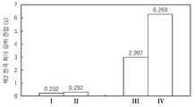
도 14는 본 발명의 일 실시예에 따른 방법으로 캐핑층 및 제3전극을 형성했을 때의 픽셀 발광 영역에서의 광투과율을 나타낸 그래프,
도 15는 본 발명의 일 실시예에 따른 방법에 따라 제3전극을 형성한 경우의 제2전극의 최대 전압 강하량을 나타낸 그래프.FIG. 1 is a cross-sectional view illustrating an organic light emitting diode display according to a preferred embodiment of the present invention,
FIG. 2 is a cross-sectional view illustrating an organic light emitting display according to another embodiment of the present invention,
FIG. 3 is a sectional view showing the organic light emitting portion of FIG. 1 or FIG. 2,
FIGS. 4 to 6 are cross-sectional views sequentially illustrating a method of manufacturing an organic light emitting display according to an embodiment of the present invention,
7 is a plan view of an organic light emitting unit according to a preferred embodiment of the present invention,
8 is a plan view of an organic light emitting unit according to another preferred embodiment of the present invention,
9 is a plan view of an organic light emitting unit according to another embodiment of the present invention,
10 is a sectional view of an organic light emitting part according to another embodiment of the present invention,
11 is a plan view of an organic light emitting part according to another preferred embodiment of the present invention,
12 is a cross-sectional view showing one pixel of Fig. 11,
13 is a plan view of an organic light emitting unit according to another embodiment of the present invention,
14 is a graph showing the light transmittance in the pixel emission region when the capping layer and the third electrode are formed by the method according to an embodiment of the present invention,
15 is a graph showing a maximum voltage drop of a second electrode when a third electrode is formed according to a method according to an embodiment of the present invention.
이하, 첨부도면을 참조하여 본 발명의 바람직한 실시예를 상세히 설명하면 다음과 같다.Hereinafter, preferred embodiments of the present invention will be described in detail with reference to the accompanying drawings.
도 1은 본 발명의 바람직한 일 실시예에 따른 유기 발광 표시장치를 도시한 단면도이다.1 is a cross-sectional view illustrating an organic light emitting display according to an embodiment of the present invention.
도 1을 참조하면, 본 발명의 바람직한 일 실시예에 따른 유기 발광 표시장치는 기판(1) 상에 형성된 유기 발광부(21)와 이 유기 발광부(21)를 밀봉하는 밀봉기판(23)을 포함한다.1, an organic light emitting display according to an embodiment of the present invention includes an organic
상기 밀봉기판(23)은 투명한 부재로 형성되어 유기 발광부(21)로부터의 화상이 구현될 수 있도록 하고, 유기 발광부(21)로 외기 및 수분이 침투하는 것을 차한다.The sealing
상기 기판(1)과 상기 밀봉기판(23)은 그 가장자리가 밀봉재(24)에 의해 결합되어 상기 기판(1)과 밀봉기판(23)의 사이 공간(25)이 밀봉된다. 상기 공간(25)에는 흡습제나 충진재 등이 위치할 수 있다.The edges of the
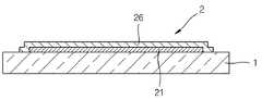
상기 밀봉기판(23) 대신에 도 2에서 볼 수 있듯이 박막의 밀봉필름(26)을 유기 발광부(21) 상에 형성함으로써 유기 발광부(21)를 외기로부터 보호할 수 있다. 상기 밀봉필름(26)은 실리콘옥사이드 또는 실리콘나이트라이드와 같은 무기물로 이루어진 막과 에폭시, 폴리이미드와 같은 유기물로 이루어진 막이 교대로 성막된 구조를 취할 수 있는 데, 반드시 이에 한정되는 것은 아니며, 투명한 박막 상의 밀봉구조이면 어떠한 것이든 적용 가능하다.As shown in FIG. 2, a sealing
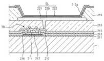
도 3은 상기 도 1 및 도 2에 도시된 유기 발광부(21)의 일 실시예를 도시한 단면도이다. 도 3에는 상기 유기 발광부(21)의 일 픽셀을 나타내었으며, 상기 유기 발광부(21)는 이러한 픽셀이 복수개 구비되어 있다.FIG. 3 is a cross-sectional view illustrating one embodiment of the organic
도 3에 따른 본 발명의 바람직한 일 실시예에 따르면, 상기 기판(1) 의 제1면(11) 상에 버퍼막(211)이 형성되고, 이 버퍼막(211) 상에 박막 트랜지스터(TR)가 형성된다.3, a
도 3에는 하나의 박막 트랜지스터(TR)만이 도시되어 있으나, 상기 픽셀은 이외에도 다른 적어도 하나의 박막 트랜지스터와 커패시터를 구비하여 픽셀 회로를 구성할 수 있다.Although only one thin film transistor TR is shown in FIG. 3, the pixel may include at least one thin film transistor and a capacitor to constitute a pixel circuit.
상기 버퍼막(211) 상에는 반도체 활성층(212)이 형성된다.A semiconductor
상기 버퍼막(211)은 불순 원소의 침투를 방지하며 표면을 평탄화하는 역할을 하는 것으로, 이러한 역할을 수행할 수 있는 다양한 물질로 형성될 수 있다. 일례로, 상기 버퍼막(211)은 실리콘 옥사이드, 실리콘 나이트라이드, 실리콘 옥시나이트라이드, 알루미늄옥사이드, 알루미늄나이트라이드, 티타늄옥사이드 또는 티타늄나이트라이드 등의 무기물이나, 폴리이미드, 폴리에스테르, 아크릴 등의 유기물 또는 이들의 적층체로 형성될 수 있다. 상기 버퍼막(211)은 필수 구성요소는 아니며, 필요에 따라서는 구비되지 않을 수도 있다.The
상기 반도체 활성층(212)은 다결정 실리콘으로 형성될 수 있는 데, 반드시 이에 한정되는 것은 아니며, 산화물 반도체로 형성될 수 있다. 예를 들면 G-I-Z-O층[(In2O3)a(Ga2O3)b(ZnO)c층](a, b, c는 각각 a≥0, b≥0, c>0의 조건을 만족시키는 실수)일 수 있다.The semiconductor
상기 반도체 활성층(212)을 덮도록 게이트 절연막(213)이 버퍼막(211) 상에 형성되고, 게이트 절연막(213) 상에 게이트 전극(214)이 형성된다.A
게이트 전극(214)을 덮도록 게이트 절연막(213) 상에 층간 절연막(215)이 형성되고, 이 층간 절연막(215) 상에 소스 전극(216)과 드레인 전극(217)이 형성되어 각각 반도체 활성층(212)과 콘택 홀을 통해 콘택된다.An interlayer insulating
상기와 같은 박막 트랜지스터(TR)의 구조는 반드시 이에 한정되는 것은 아니며, 다양한 형태의 박막 트랜지스터의 구조가 적용 가능함은 물론이다. 예컨대, 상기 박막 트랜지스터(TR)는 탑 게이트 구조로 형성된 것이나, 게이트 전극(214)이 반도체 활성층(212) 하부에 배치된 바텀 게이트 구조로 형성될 수도 있다. 물론 이 밖에도 적용 가능한 모든 박막 트랜지스터의 구조가 적용될 수 있음은 물론이다.The structure of the thin film transistor TR is not limited thereto, and various structures of the thin film transistor may be applied. For example, the thin film transistor TR may be formed in a top gate structure, or may be formed in a bottom gate structure in which a
상기 박막 트랜지스터(TR)와 함께 커패시터를 포함하는 픽셀 회로(미도시)가 형성될 수 있다.A pixel circuit (not shown) including a capacitor together with the thin film transistor TR may be formed.
이러한 박막 트랜지스터(TR)를 포함하는 픽셀 회로를 덮도록 제1절연막(218)이 형성된다. 상기 제1절연막(218)은 상면이 평탄화된 단일 또는 복수층의 절연막이 될 수 있다. 이 제1절연막(218)은 무기물 및/또는 유기물로 형성될 수 있다.A first insulating
상기 제1절연막(218) 상에는 도 3에서 볼 수 있듯이, 박막 트랜지스터(TR)를 포함하는 픽셀 회로와 전기적으로 연결된 제1전극(221)이 형성된다. 상기 제1전극(221)은 각 픽셀마다 서로 독립된 아일랜드 형태로 형성된다.As shown in FIG. 3, a
상기 제1절연막(218) 상에는 상기 제1전극(221)의 가장자리를 덮도록 제2절연막(219)이 형성된다. 상기 제2절연막(219)에는 개구(219a)가 형성되어 제1전극(221)의 가장자리를 제외한 중앙부를 노출시킨다.A second insulating
개구(219a)를 통해 노출된 제1전극(221) 상에는 유기막(220)이 형성되고 상기 유기막(220)을 덮도록 제2전극(222)이 형성되어 유기 발광 소자(EL)를 형성한다.An
상기 유기막(220)은 저분자 또는 고분자 유기막이 사용될 수 있다. 저분자 유기막을 사용할 경우, 홀 주입층(HIL: Hole Injection Layer), 홀 수송층(HTL: Hole Transport Layer), 발광층(EML: Emission Layer), 전자 수송층(ETL: Electron Transport Layer), 전자 주입층(EIL: Electron Injection Layer) 등이 단일 혹은 복합의 구조로 적층되어 형성될 수 있다. 이들 저분자 유기막은 진공증착의 방법으로 형성될 수 있다. 이 때, 상기 발광층은 적, 녹, 청색의 픽셀마다 독립되게 형성되고, 홀 주입층, 홀 수송층, 전자 수송층, 및 전자 주입층 등은 공통층으로서, 적, 녹, 청색의 픽셀에 공통으로 적용될 수 있다.The
상기 정공주입층(HIL)은 구리프탈로시아닌 등의 프탈로시아닌 화합물 또는 스타버스트(Starburst)형 아민류인 TCTA, m-MTDATA, m-MTDAPB 등으로 형성할 수 있다.The hole injection layer (HIL) may be formed of a phthalocyanine compound such as copper phthalocyanine or starburst type amines such as TCTA, m-MTDATA, m-MTDAPB and the like.
상기 정공 수송층(HTL)은 N,N'-비스(3-메틸페닐)- N,N'-디페닐-[1,1-비페닐]-4,4'-디아민(TPD), N,N'-디(나프탈렌-1-일)-N,N'-디페닐 벤지딘(α-NPD)등으로 형성될 수 있다.The hole transport layer (HTL) may be formed by a combination of N, N'-bis (3-methylphenyl) -N, N'-diphenyl- [1,1- biphenyl] -4,4'- diamine (TPD) -Di (naphthalene-1-yl) -N, N'-diphenylbenzidine (? -NPD).
상기 전자 주입층(EIL)은 LiF, NaCl, CsF, Li2O, BaO, Liq 등의 물질을 이용하여 형성할 수 있다.The electron injection layer (EIL) may be formed using a material such as LiF, NaCl, CsF, Li2O, BaO, Liq, or the like.
상기 전자 수송층(ETL)은 Alq3를 이용하여 형성할 수 있다.The electron transport layer (ETL) can be formed using Alq3.
상기 발광층(EML)은 호스트 물질과 도판트 물질을 포함할 수 있다.The light emitting layer (EML) may include a host material and a dopant material.
상기 호스트 물질로는 트리스(8-히드록시-퀴놀리나토)알루미늄 (Alq3), 9,10-디(나프티-2-일)안트라센 (AND), 3-Tert-부틸-9,10-디(나프티-2-일)안트라센 (TBADN), 4,4'-비스(2,2-디페닐-에텐-1-일)-4,4'-디메틸페닐 (DPVBi), 4,4'-비스Bis(2,2-디페닐-에텐-1-일)-4,4'-디메틸페닐 (p-DMDPVBi), Tert(9,9-디아릴플루오렌)s (TDAF), 2-(9,9'-스피로비플루오렌-2-일)-9,9'-스피로비플루오렌 (BSDF), 2,7-비스(9,9'-스피로비플루오렌-2-일)-9,9'-스피로비플루오렌 (TSDF), 비스(9,9-디아릴플루오렌)s (BDAF), 4,4'-비스(2,2-디페닐-에텐-1-일)-4,4'-디-(tert-부틸)페닐 (p-TDPVBi), 1,3-비스(카바졸-9-일)벤젠 (mCP), 1,3,5-트리스(카바졸-9-일)벤젠 (tCP), 4,4',4"-트리스(카바졸-9-일)트리페닐아민 (TcTa), 4,4'-비스(카바졸-9-일)비페닐 (CBP), 4,4'-비스Bis(9-카바졸일)-2,2'-디메틸-비페닐 (CBDP), 4,4'-비스(카바졸-9-일)-9,9-디메틸-플루오렌 (DMFL-CBP), 4,4'-비스(카바졸-9-일)-9,9-비스bis(9-페닐-9H-카바졸)플루오렌 (FL-4CBP), 4,4'-비스(카바졸-9-일)-9,9-디-톨일-플루오렌 (DPFL-CBP), 9,9-비스(9-페닐-9H-카바졸)플루오렌 (FL-2CBP) 등이 사용될 수 있다.Examples of the host material include tris (8-hydroxy-quinolinato) aluminum (Alq3), 9,10-di (naphthyl-2-yl) anthracene (AND), 3-tert- Bis (2,2-diphenyl-ethen-1-yl) -4,4'-dimethylphenyl (DPVBi), 4,4'-bis Bis (P-DMDPVBi), Tert (9,9-diarylfluorene) s (TDAF), 2- (9,9 (9,9'-spirobifluoren-2-yl) -9,9'-spirobifluorene (BSDF), 2,7- (TSDF), bis (9,9-diarylfluorene) s (BDAF), 4,4'-bis (2,2- (P-TDPVBi), 1,3-bis (carbazol-9-yl) benzene (mCP), 1,3,5-tris (carbazol-9-yl) benzene (carbazole-9-yl) biphenyl (CBP), 4,4'-bis (carbazole-9-yl) -Bis Bis (9-carbazolyl) -2,2'-dimethyl-biphenyl (CBDP), 4,4'-bis (carbazol- CBP), (9-phenyl-9H-carbazole) fluorene (FL-4CBP), 4,4'-bis (carbazole-9-yl) -9,9-di-tolyl-fluorene (DPFL-CBP) and 9,9-bis (9-phenyl-9H-carbazol) fluorene (FL-2CBP).
상기 도판트 물질로는 DPAVBi (4,4'-비스[4-(디-p-톨일아미노)스티릴]비페닐), ADN (9,10-디(나프-2-틸)안트라센), TBADN (3-터트-부틸-9,10-디(나프-2-틸)안트라센) 등이 사용될 수 있다.Examples of the dopant material include DPAVBi (4,4'-bis [4- (di-p-tolylamino) styryl] biphenyl), ADN (9,10- (3-tert-butyl-9,10-di (naphth-2-yl) anthracene).
상기 제1전극(221)은 애노우드 전극의 기능을 하고, 상기 제2전극(222)은 캐소오드 전극의 기능을 할 수 있는 데, 물론, 이들 제1전극(221)과 제2전극(222)의 극성은 서로 반대로 되어도 무방하다.The
상기 제1전극(221)이 애노드 전극의 기능을 할 경우, 상기 제1전극(221)은 일함수가 높은 ITO, IZO, ZnO, 또는 In2O3 등을 포함하여 구비될 수 있다. 만일 도 3에서 기판(1)의 반대 방향으로 화상이 구현되는 전면 발광형일 경우 상기 제1전극(221)은 Ag, Mg, Al, Pt, Pd, Au, Ni, Nd, Ir, Cr, Li, Yb 또는 Ca 등으로 형성된 반사막을 더 포함할 수 있다.When the
상기 제2전극(222)이 캐소드 전극의 기능을 할 경우, 상기 제2전극(222)은 Ag, Mg, Al, Pt, Pd, Au, Ni, Nd, Ir, Cr, Li, 또는 Ca의 금속으로 형성될 수 있다. 만일 도 3에서 전면 발광형일 경우, 상기 제2전극(222)은 광투과가 가능하도록 구비되어야 한다. 이를 위해, 상기 제2전극(222)은 투명한 금속산화물인 ITO, IZO, ZnO, 또는 In2O3 등을 포함하여 구비될 수 있다. 또는 상기 제2전극(222)은 Al, Ag 및/또는 Mg를 이용하여 박막으로 형성할 수 있다. 예컨대 Mg:Ag 및/또는 Ag가 단일층 또는 적층 구조로 형성될 수 있다. 상기 제2전극(222)은 제1전극(221)과 달리 모든 픽셀들에 걸쳐 공통된 전압이 인가되도록 형성되는 데, 이를 위해 픽셀 마다 패터닝되지 않은 공통 전극으로 형성된다. 물론 공통 전극인 상기 제2전극(222)을 발광 영역에 대응되는 영역 이외의 영역이 제거된 메쉬(Mesh) 형태로 패터닝할 수도 있다.When the
전술한 전면 발광형일 경우, 상기 제2전극(222)이 투명한 금속산화물 또는 박막의 금속을 포함하기 때문에, 제2전극(222)이 공통 전극으로 형성될 경우, 제2전극(222)의 면저항이 커지게 되어 전압 강하 현상이 발생되게 된다. 본 발명은 이러한 문제를 해결하기 위하여 상기 제2전극(222)과 전기적으로 연결되도록 제3전극(223)을 더 형성하였다.When the
그리고 제2전극(222)의 상면이 도 1에서의 밀봉 기판(23)에 의해 손상될 우려가 있다. 뿐만 아니라, 도 2와 같이 밀봉필름(26)을 형성하는 경우에도 밀봉필름(26)의 형성 시에 제2전극(222)이 손상받기 쉽다. 본 발명은 이러한 문제를 해결하기 위하여, 상기 제2전극(222) 상에 캐핑층(224)을 형성하였다.And the upper surface of the
상기 캐핑층(224)은 제2전극(222) 상의 제1영역(R1) 상에 형성되고, 제1가장자리(224a)를 갖는다.The
상기 제3전극(223)은 상기 제2전극(222) 상의 제2영역(R2) 상에 형성되고, 제2가장자리(223a)를 갖는다. 상기 제3전극(223)은 상기 캐핑층(224)과 수평인 상태로 서로 인접하게 배치된다.The
상기 제1영역(R1)은 적어도 하나의 픽셀에서 발광이 일어나는 면적보다 넓으며, 상기 하나의 픽셀에서 발광이 일어나는 영역을 덮는 영역에 해당한다. 상기 제1영역(R1) 전체에 캐핑층(224)이 형성되며, 제1영역(R1)의 가장자리는 캐핑층(224)의 제1가장자리(224a)가 된다. 그리고 상기 제2영역(R2)은 상기 제2전극(222) 중 제1영역(R1) 이외의 영역에 해당하는 데, 상기 제2영역(R2) 전체에 제3전극(223)이 형성되며, 제2영역(R2)의 가장자리는 제3전극(223)의 제2가장자리(223a)가 된다. 상기 제2영역(R2)은 발광이 일어나는 영역을 제외한 영역이 된다.The first region R1 is larger than an area where light emission occurs in at least one pixel, and corresponds to an area covering an area where light emission occurs in the one pixel. A
상기 캐핑층(224)의 제1가장자리(224a)의 측면과 상기 제3전극(223)의 제2가장자리(223a)의 측면은 서로 맞닿은 상태가 된다.The side of the
상기 제3전극(223)은 제2전극(222)의 면저항을 줄일 수 있도록 상기 제2전극(222)의 두께보다 두껍게 형성하는 것이 바람직하다.The
그리고 상기 캐핑층(224)은 픽셀에서 발광이 일어나는 영역을 덮는 것이므로, 광투과가 가능하도록 형성되는 것이 바람직하다. 상기 캐핑층(224)은 상기 제3전극(223)보다 얇게 박막으로 형성될 수 있으나, 반드시 이에 한정되는 것은 아니다.Since the
본 발명의 일 실시예에 있어, 상기 제3전극(223)과 상기 캐핑층(224) 간의 접착력은 상기 제3전극(223)과 상기 제2전극(222) 간의 접착력보다 약한 것이 되도록 물질을 선택한다.The adhesion between the
이를 위해, 상기 캐핑층(224)은 8-퀴놀리나토리튬(Liq: 8-Quinolinolato Lithium), N,N-디페닐-N,N-비스(9-페닐-9H-카바졸-3-일)비페닐-4,4'-디아민(HT01: N,N-diphenyl-N,N-bis(9-phenyl-9H-carbazol-3-yl)biphenyl-4,4'-diamine), N(디페닐-4-일)9,9-디메틸-N-(4(9-페닐-9H-카바졸-3-일)페닐)-9H-플루오렌-2-아민(HT211: N(diphenyl-4-yl)9,9-dimethyl-N-(4(9-phenyl-9H-carbazol-3-yl)phenyl)-9H-fluorene-2-amine), 또는 2-(4-(9,10-디(나프탈렌-2-일)안트라센-2-일)페닐)-1-페닐-1H-벤조-[D]이미다졸(LG201: 2-(4-(9,10-di(naphthalene-2-yl)anthracene-2-yl)phenyl)-1-phenyl-1H-benzo-[D]imidazole)을 포함하는 물질로 형성될 수 있다.To this end, the
그리고 상기 제3전극(223)은 Mg로 형성될 수 있다.The
제3전극(223)이 되는 Mg는 제2전극(222)과는 같은 금속이므로, 접착성이 좋다. 그러나, Mg는 전술한 캐핑층(224)의 물질과는 접착이 잘 되지 않는다. 따라서 이러한 제3전극(223) 및 캐핑층(224) 간의 접착력 특성을 이용하여 제3전극(223)을 간단하게 패터닝할 수 있다.The Mg that becomes the
전술한 바와 같이 제3전극(223)은 제2영역(R2)에만 형성되도록 패터닝되어야 한다. 그런데, 유기 발광 소자(EL)의 유기막(220)을 형성한 후에는 통상의 금속막의 패터닝 방법으로 많이 사용되는 포토 리소그래피와 같은 습식 공정을 이용하여 상기 제3전극(223)을 패터닝할 수 없다. 이는 습식 공정으로 유기막(220)에 수분 및/또는 산소가 침투되면 유기 발광 소자(EL)의 수명이 급격히 저하되기 때문이다.The
이 때문에, 실제 공정에서는 상기 제3전극(223)의 패터닝이 매우 어렵게 된다.Therefore, in the actual process, patterning of the
본 발명은 제3전극(223) 및 캐핑층(224) 간의 접착력 특성을 이용하여 제3전극(223)을 간단하게 패터닝할 수 있다. 이하 그 방법을 보다 상세히 설명한다.The present invention can easily pattern the
먼저, 도 4에서 볼 수 있듯이, 제2전극(222)까지 형성한 다음, 여기에 도 5에서 볼 수 있듯이, 마스크(3)를 이용하여 캐핑층(224)을 형성한다. 상기 캐핑층(224)은 전술한 유기물로 형성될 수 있기 때문에, 마스크(3)를 이용한 열증착(thermal evaporation) 방법으로 형성할 수 있다. 상기 마스크(3)에는 캐핑층(224)의 패턴에 대응되도록 개구(31)가 형성되어 있고, 이 개구(31)를 통해 캐핑층(224)을 형성하게 될 물질(M1)이 증착되어 캐핑층(224)을 형성하게 된다.First, as shown in FIG. 4, a
다음으로, 도 6에서 볼 수 있듯이, 제3전극(223) 형성용 물질(M2)을 전체적으로 성막한다. 이 때에는 도면에 도시하지는 않았지만 모든 픽셀들에 대해 개방된 오픈 마스크를 이용하여 상기 물질(M2)을 성막하거나, 마스크 없이 물질(M2)을 성막할 수 있다.Next, as shown in FIG. 6, the material M2 for forming the
이 경우, 제3전극(223) 형성용 물질(M2)은 캐핑층(224)과 접착력이 나쁘기 때문에 캐핑층(224) 상에는 성막되지 않으며, 상대적으로 접착력이 좋은 제2전극(222) 위에만 성막된다.In this case, the material M2 for forming the
따라서 제3전극(223)은 별도의 마스크나 패터닝 공정 없이도 자연스럽게 패터닝이 될 수 있다.Therefore, the
상기 캐핑층(224)은 도 7에서 볼 수 있듯이, 하나의 픽셀(P)당 하나씩 존재하는 아일랜드 형태로 구비될 수 있다. 도 7에는 캐핑층(224)이 하나의 픽셀(P) 전체를 덮는 면적으로 되어 있으나, 반드시 이에 한정되는 것은 아니고 전술한 바와 같이 하나의 픽셀(P)의 발광이 일어나는 면적을 덮도록 하면 무방하다.As shown in FIG. 7, the
이 경우 제3전극(223)은 각 픽셀(P)들 사이로 격자 패턴을 이루게 된다.In this case, the
상기 캐핑층(224)은 도 8에서 볼 수 있듯이, 복수의 픽셀(P) 당 하나씩 존재하는 아일랜드 형태로 구비될 수 있다. 이 경우 제3전극(223)은 복수 픽셀(P)들 사이로 지나가는 격자 패턴을 이루게 된다.As shown in FIG. 8, the
상기 캐핑층(224)은 도 9에서 볼 수 있듯이, 일렬로 배치된 복수의 픽셀(P)들을 덮을 수 있도록 스트라이프 형태로 구비될 수 있다. 이 경우 제3전극(223)은 각 픽셀 열 사이로 지나가는 스트라이프 패턴을 이루게 된다.As shown in FIG. 9, the
도 9의 변형예로서, 비록 도시하지는 않았지만, 상기 캐핑층(224)이 가로 방향으로 복수의 픽셀(P)들을 더 덮도록 스트라이프 형태로 구비될 수 있다.As a modification of FIG. 9, although not shown, the
한편, 도 6에서와 같이 제3전극(223) 형성용 물질(M2)을 증착할 경우, 상기 제3전극(223)은 캐핑층(224) 이외의 영역에만 성막되는 것 뿐 아니라, 도 10에서 볼 수 있듯이, 캐핑층(224) 상에도 캐핑층 이외의 영역에 형성된 제3전극(223)의 제1두께(t1)보다 얇은 제2두께(t2)를 갖는 박막(223')이 형성될 수 있다. 이는 비록 제3전극(223) 형성용 물질(M2)이 캐핑층(224)과 접착력이 나쁘기 때문에, 이론적으로는 캐핑층(224) 상에는 성막되지 않고, 상대적으로 접착력이 좋은 제2전극(222) 위에만 성막된다고 하더라도, 도 6과 같은 공정은 별도의 패터닝 마스크를 이용하지 않고 오픈 마스크를 이용하여 증착하는 것이기 때문에 상기 캐핑층(224) 위에 제2두께(t2)를 갖는 박막(223')이 얇게 물리적으로 얹혀져 형성될 수는 있기 때문이다.6, when the material M2 for forming the
상기 제2두께(t2)는 제1두께(t1)보다 얇기 때문에 제1영역(R1)에서 유기 발광 소자(EL)의 휘도에 큰 영향을 미치지 않을 수 있다.Since the second thickness t2 is thinner than the first thickness t1, the brightness of the organic light emitting diode EL in the first region R1 may not be significantly affected.
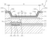
도 11은 본 발명의 바람직한 또 다른 일 실시예에 따른 유기 발광 표시장치의 유기 발광부(21)의 평면도이고, 도 12는 도 11의 일 픽셀을 도시한 단면도이다.FIG. 11 is a plan view of an organic
도 11 및 도 12에서 볼 때, 본 발명의 바람직한 또 다른 일 실시예에 따르면, 상기 유기 발광부(21)는 외광이 투과되도록 구비된 투과 영역(TA)과, 이 투과 영역(TA)을 사이에 두고 서로 이격된 복수의 픽셀 영역(PA)들로 구획된다.11 and 12, according to another preferred embodiment of the present invention, the organic
도 11에서 볼 수 있듯이, 각 픽셀 영역(PA) 내에는 픽셀 회로부(PC)가 위치하며, 스캔 라인(S), 데이터 라인(D) 및 Vdd 라인(V)과 같은 복수의 도전 라인들이 이 픽셀 회로부(PC)에 전기적으로 연결된다. 도면에 도시하지는 않았지만 상기 픽셀 회로부(PC)의 구성에 따라 상기 스캔 라인(S), 데이터 라인(D) 및 구동전원인 Vdd 라인(V) 외에도 더 다양한 도전 라인들이 구비되어 있을 수 있다.11, a pixel circuit portion PC is located in each pixel region PA, and a plurality of conductive lines, such as a scan line S, a data line D, and a Vdd line V, And is electrically connected to the circuit portion PC. Although not shown in the drawing, according to the configuration of the pixel circuit part PC, more various conductive lines may be provided in addition to the scan line S, the data line D, and the Vdd line V as a driving power source.
도 11에서 볼 수 있듯이, 상기 픽셀 회로부(PC)는, 스캔 라인(S)과 데이터 라인(D)에 연결된 제1박막 트랜지스터(T1)와, 제1박막 트랜지스터(T1)와 Vdd 라인(V)에 연결된 제2박막 트랜지스터(T2)와, 제1박막 트랜지스터(T1)와 제2박막 트랜지스터(T2)에 연결된 커패시터(Cst)를 포함한다. 이 때, 제1박막 트랜지스터(T1)는 스위칭 트랜지스터가 되고, 제2박막 트랜지스터(T2)는 구동 트랜지스터가 된다. 상기 제2박막 트랜지스터(T2)는 제1전극(221)과 전기적으로 연결되어 있다. 도 10에서 제1박막 트랜지스터(T1)와 제2박막 트랜지스터(T2)는 P형으로 형성될 수 있는 데, 반드시 이에 한정되는 것은 아니며 적어도 하나가 N형으로 형성될 수도 있다. 상기와 같은 박막 트랜지스터 및 커패시터의 개수는 반드시 도시된 실시예에 한정되는 것은 아니며, 픽셀 회로부(PC)에 따라 2 이상의 박막 트랜지스터, 1 이상의 커패시터가 조합될 수 있다.11, the pixel circuit part PC includes a first thin film transistor T1 connected to the scan line S and the data line D, a first thin film transistor T1 connected to the first thin film transistor T1 and a Vdd line V, A second thin film transistor T2 connected to the first thin film transistor T1 and a capacitor Cst connected to the second thin film transistor T2. At this time, the first thin film transistor T1 becomes a switching transistor and the second thin film transistor T2 becomes a driving transistor. The second thin film transistor T2 is electrically connected to the
도 11에 따르면, 스캔 라인(S)이 제1전극(221)과 중첩되게 배치된다. 그러나, 본 발명은 반드시 이에 한정되는 것은 아니며, 스캔 라인(S), 데이터 라인(D) 및 Vdd 라인(V)을 포함한 복수의 도전 라인들 중 적어도 어느 하나가 상기 제1전극(221)과 중첩되도록 배치시킬 수 있으며, 경우에 따라서는 스캔 라인(S), 데이터 라인(D) 및 Vdd 라인(V)을 포함한 복수의 도전 라인들 모두 제1전극(221)과 중첩되거나 제1전극(221) 옆에 배치시킬 수 있다.Referring to FIG. 11, the scan line S overlaps with the
본 실시예는 이처럼 픽셀 영역(PA)과 투과 영역(TA)의 분리에 따라 투과 영역(TA)을 통해 외부를 관찰할 때에, 외부광이 픽셀 회로부(PC) 내의 소자들의 패턴과 관련하여 산란함에 따라 발생되는 외부 이미지 왜곡 현상을 방지할 수 있다.This embodiment differs from the first embodiment in that external light is scattered in relation to the pattern of the elements in the pixel circuit portion PC when the outside is observed through the transmission region TA in accordance with the separation of the pixel region PA and the transmission region TA It is possible to prevent an external image distortion phenomenon that is generated.
이러한 픽셀 영역(PA)과 투과 영역(TA)의 전체 면적 대비 투과 영역(TA)의 면적의 비율이 5% 내지 90% 범위에 속하도록 픽셀 영역(PA)과 투과 영역(TA)이 형성된다.The pixel area PA and the transmissive area TA are formed such that the ratio of the area of the transmissive area TA to the total area of the pixel area PA and the transmissive area TA falls within the range of 5% to 90%.
픽셀 영역(PA)과 투과 영역(TA)의 전체 면적 대비 투과 영역(TA)의 면적의 비율이 5% 보다 작으면, 유기 발광부(21)를 투과할 수 있는 빛이 적어 사용자가 반대 측에 위치한 사물 또는 이미지를 보기 어렵다. 즉, 유기 발광부(21)가 투명하다고 표현하기는 어렵다. 그러나 투과 영역(TA)의 면적이 픽셀 영역(PA)과 투과 영역(TA)의 전체 면적 대비 5% 정도라 하더라도 실제로는 외부광의 세기가 강하면 사용자가 디스플레이를 투과하여 반대측에 위치한 사물 또는 이미지를 충분히 인식할 수 있으므로 사용자는 투명 디스플레이로서 인식이 가능하게 된다. 그리고, 후술하는 바와 같이 픽셀 회로부(PC)에 구비되는 박막 트랜지스터를 산화물 반도체와 같이 투명 박막 트랜지스터로 형성하고, 유기 발광 소자도 투명 소자로 형성할 경우에는 더욱 투명 디스플레이로서의 인식이 커질 수 있다.If the ratio of the area of the transmissive area TA to the total area of the pixel area PA and the transmissive area TA is less than 5%, there is less light that can be transmitted through the organic
픽셀 영역(PA)과 투명 영역(TA)의 전체 면적 대비 투명 영역(TA)의 면적의 비율이 90% 보다 크면 유기 발광부(21)의 픽셀 집적도가 지나치게 낮아져 픽셀 영역(PA)에서의 발광을 통해 안정적인 화상을 구현하기 어렵다. 즉, 픽셀 영역(PA)의 면적이 작아질수록, 화상을 구현하기 위해서는 유기막(220)에서 발광하는 빛의 휘도가 높아져야 한다. 이와 같이, 유기 발광 소자를 고휘도 상태로 작동시키면 수명이 급격히 저하되는 문제점이 생긴다.If the ratio of the area of the transparent area TA to the total area of the pixel area PA and the transparent area TA is greater than 90%, the pixel density of the organic
상기 픽셀 영역(PA)과 투과 영역(TA)의 전체 면적 대비 투과 영역(TA)의 면적의 비율은 20% 내지 70%의 범위에 속하도록 하는 것이 바람직하다.The ratio of the area of the transmissive area TA to the total area of the pixel area PA and the transmissive area TA is preferably in the range of 20% to 70%.
20% 미만에서는 투과 영역(TA)에 비해 상기 픽셀 영역(PA)의 면적이 지나치게 크므로, 사용자가 투과 영역(TA)을 통해 외부 이미지를 관찰하는 데에 한계가 있다. 70%를 초과할 경우 픽셀 영역(PA) 내에 배치할 픽셀 회로부(PC) 설계에 많은 제약이 따르게 된다.If the area is less than 20%, the area of the pixel area PA is excessively larger than the transmissive area TA, which limits the user's ability to observe the external image through the transmissive area TA. If it exceeds 70%, there are many restrictions on the design of the pixel circuit portion (PC) to be disposed in the pixel region PA.
상기 픽셀 영역(PA)에는 픽셀 회로부(PC)와 전기적으로 연결된 제1전극(221)이 구비되며, 상기 픽셀 회로부(PC)는 상기 픽셀 전극(221)에 가리워지도록 상기 제1전극(221)과 중첩된다. 그리고, 전술한 스캔 라인(S), 데이터 라인(D) 및 Vdd 라인(V)을 포함하는 도전 라인들 중 적어도 하나가 이 픽셀 전극(221)을 지나가도록 배치될 수 있다. 물론, 이들 도전 라인들은 픽셀 회로부(PC)에 비해 투과율을 저해하는 비율이 적기 때문에 설계 조건에 따라서는 모두 제1전극(221)에 인접하게 배치시킬 수 있다.The pixel region PA is provided with a
전술한 바와 같이, 만일 제1전극(221)은 광 반사가 가능한 도전성 금속으로 이루어진 반사막을 포함하는 경우, 제1전극(221)이 픽셀 회로부(PC)를 가려주고, 픽셀 영역(PA)에서의 픽셀 회로부(PC)에 의한 외부 이미지 왜곡 등을 차단한다.As described above, if the
도 12에서 볼 수 있듯이, 제1영역(R1) 내에 픽셀 영역(PA)과 투과 영역(TA)이 위치한다.As can be seen from Fig. 12, the pixel region PA and the transmissive region TA are located in the first region R1.
이 때, 상기 캐핑층(224)은 제1영역(R1) 내에 위치하므로, 픽셀 영역(PA)과 투과 영역(TA)을 모두 덮게 된다. 그리고, 상기 제3전극(223)은 제1영역(R1) 외측의 제2영역(R2)에 구비된다.At this time, since the
이러한 실시예에 있어서, 상기 캐핑층(224)은 전술한 바와 같이 투명한 유기물을 사용하므로 투과 영역(TA)에서의 광투과도에 영향을 미치지 않을 수 있다. 캐핑층(224) 및 제3전극(223)의 재질 및 형성 방법 등은 전술한 실시예들과 동일하다.In this embodiment, since the
한편, 비록 도면으로 도시하지는 않았지만, 상기 투과 영역(TA)에는 적어도 제2전극(222)의 일부가 제거된 투과창이 형성되어, 투과 영역(TA)에서의 광투과도를 더욱 높일 수 있다. 이 때, 투과창은 반드시 제2전극(222)만 제거되는 것에 그치지 않고, 제2절연막(219), 제1절연막(218), 층간 절연막(215), 게이트 절연막(213) 및 버퍼막(211) 중 적어도 하나의 막에 더 형성될 수 있다.Although not shown in the drawing, a transmissive window in which at least a portion of the
도 13은 도 11 및 도 12를 참조로 설명한 투명형 유기 발광 표시장치의 또 다른 일 실시예를 도시한 것이다.FIG. 13 shows another embodiment of the transparent organic light emitting display device described with reference to FIGS. 11 and 12. FIG.
도 13의 실시예는 적, 녹, 청색의 세 개의 서브 픽셀에 의해 하나의 픽셀이 구현되어 백색 광을 낼 수 있는 경우를 나타낸다. 물론, 적, 녹, 청색 이외에도 다른 색상에 의해 백색 광을 내는 경우를 포함한다.13 shows a case where one pixel is implemented by three subpixels of red, green, and blue to emit white light. Of course, other than red, green, and blue colors, white light is emitted by different colors.
이 경우, 세 개의 서브 픽셀들의 제1전극들(221a)(221b)(221c) 당 하나의 투과 영역(TA)이 형성된다. 제1데이터 라인(D1) 내지 제3데이터 라인(D3)은 각각 상기 세 개의 서브 픽셀들의 제1전극들(221a)(221b)(221c)에 전기적으로 연결된다. 그리고 제1Vdd라인(V1)은 첫번째 제1전극(221a) 및 두번째 제1전극(221b)에 전기적으로 연결되고, 제2Vdd라인(V2)은 세번째 제1전극(221c)에 전기적으로 연결된다.In this case, one transmission region TA is formed for each of the
이러한 구조의 경우 복수의 서브픽셀에 대하여 하나의 큰 투과 영역(TA)을 구비하고 있으므로, 전체 디스플레이의 투과율을 더욱 높일 수 있고, 광산란에 의한 이미지 왜곡 효과도 더욱 줄일 수 있다.In this structure, since one large transmissive area TA is provided for a plurality of subpixels, the transmissivity of the entire display can be further increased, and the image distortion effect due to light scattering can be further reduced.
도 13에는 도시하지 않았지만, 상기 투과 영역(TA)에도 전술한 바와 같이 적어도 제2전극의 일부가 제거된 하나의 큰 투과창이 형성될 수 있다. 이 때, 투과창은 반드시 제2전극만 제거되는 것에 그치지 않고, 제2절연막, 제1절연막, 층간 절연막, 게이트 절연막 및 버퍼막 중 적어도 하나의 막에 더 형성될 수 있다.Although not shown in FIG. 13, a single large transmissive window in which at least a portion of the second electrode is removed may be formed in the transmissive region TA as described above. At this time, the transmission window may be formed not only on the second electrode but also on at least one of the second insulating film, the first insulating film, the interlayer insulating film, the gate insulating film, and the buffer film.
도 11 내지 도 13에 따른 실시예에서도 도 10에서와 같이 제1영역(R1)의 캐핑층(224) 상에도 제3전극 형성용 물질로 이루어진 보다 얇은 두께의 박막이 형성될 수도 있다. 이 경우에도 전술한 바와 같이 상기 박막의 두께가 매우 얇기 때문에 투과 영역(TA)에서의 광투과율 등에 큰 영향을 미치지 않을 수 있다.In the embodiment according to FIGS. 11 to 13, a thinner thin film made of the third electrode forming material may also be formed on the
도 14는 도 4 내지 도 7의 방법으로 캐핑층(224) 및 제3전극(223)을 형성했을 때의 픽셀 발광 영역에서의 광투과율을 나타낸 것이다.FIG. 14 shows the light transmittance in the pixel emission region when the
캐핑층(224)으로는 전술한 각 캐핑층 물질을 사용하였으며, 30Å의 두께로 증착하였다. 제3전극(223)은 오픈 마스크를 이용하여 Mg을 전 픽셀 영역에 증착하여 형성하였는 데, Mg 1,000Å을 증착하였다.As the
도 14에서 볼 수 있듯이, 가시광 전 파장 영역에서 거의 100% 에 가까운 광투과율을 나타냄을 알 수 있다. 이는 전술한 바와 같이 캐핑층(224)이 형성된 영역에는 Mg이 거의 증착되지 않았다는 것을 알 수 있다.As can be seen from FIG. 14, it can be seen that the light transmittance is close to 100% in the visible light wavelength region. As described above, it can be seen that almost no Mg is deposited in the region where the
따라서 본 발명의 경우, 광 손실 없이도 캐핑층(224)과 제3전극(223)을 효과적으로 형성할 수 있게 된다.Therefore, in the present invention, the
도 15는 본 발명에 따라 제3전극(223)을 형성한 경우의 제2전극의 최대 전압 강하량을 나타낸 것이다. 각 예에서 제2전극(222)은 Mg:Ag/Ag로, 면저항이 20ohm/sq가 되도록 형성하였다.15 shows the maximum voltage drop amount of the second electrode when the
실험예 Ⅰ은 19inch 크기의 디스플레이에서 도 3 및 도 7과 같은 형태로 캐핑층(224) 및 제3전극(223)을 형성한 것이다. 이 때의 제3전극(223)은 Mg 3,500Å을 증착한 것이다.Experimental Example I shows a
실험예 Ⅱ는 40inch 크기의 디스플레이에서 도 3 및 도 7과 같은 형태로 캐핑층(224) 및 제3전극(223)을 형성한 것이다. 이 때의 제3전극(223)은 Mg 3,500Å을 증착한 것이다.Experimental Example II shows a
비교예 Ⅲ은 19inch 크기의 디스플레이에서 캐핑층(224) 및 제3전극(223)을 형성하지 않은 것이다.Comparative Example III does not form the
비교예 Ⅳ은 40inch 크기의 디스플레이에서 캐핑층(224) 및 제3전극(223)을 형성하지 않은 것이다.Comparative Example IV does not form the
위 14에서 볼 수 있듯이, 본 발명에 따른 실험예 Ⅰ 및 Ⅱ의 제2전극 전압 감소량이 비교예 Ⅲ 및 Ⅳ의 제2전극 전압 감소량에 비해 현격히 낮음을 알 수 있다.As shown in the above 14, it can be seen that the second electrode voltage reduction amount in Experiments I and II according to the present invention is significantly lower than the second electrode voltage reduction amount in Comparative Examples III and IV.
이상은 전면 발광형을 중심으로 설명한 것이나, 본 발명은 반드시 이에 한정되는 것은 아니고, 기판(1)의 방향으로 화상이 구현되는 배면 발광형 및 양 방향으로 화상이 구현되는 양면 발광형에도 동일하게 적용 가능하다.However, the present invention is not necessarily limited to this. The same applies also to a back light emitting type in which an image is realized in the direction of the
본 발명은 도면에 도시된 일 실시예를 참고로 하여 설명하였으나 이는 예시적인 것에 불과하며 당해 분야에서 통상의 지식을 가진 자라면 이로부터 다양한 변형 및 실시예의 변형이 가능하다는 점을 이해할 것이다.While the present invention has been particularly shown and described with reference to exemplary embodiments thereof, it will be understood by those skilled in the art that various changes and modifications may be made therein without departing from the scope of the present invention.
Claims (35)
Translated fromKorean상기 기판 상에 구비된 박막 트랜지스터;
상기 박막 트랜지스터를 덮는 제1절연막;
상기 제1절연막 상에 형성되고, 상기 박막 트랜지스터와 전기적으로 연결된 제1전극;
상기 제1전극을 덮도록 상기 제1절연막 상에 형성되고 상기 제1전극의 일부를 노출시키는 개구를 갖는 제2절연막;
상기 제2절연막 상의 일부 및 상기 제1전극 상에 형성된 유기 발광층;
상기 제2절연막 및 유기 발광층 상에 형성된 제2전극;
상기 제2전극 상의 제1영역 상에 형성되고 제1가장자리를 갖는 캐핑층; 및
상기 제2전극 상의 상기 제1영역 이외의 영역인 제2영역 상에 형성되고, 상기 캐핑층의 제1가장자리의 측면과 그 측면이 서로 맞닿은 제2가장자리를 갖는 제3전극;을 포함하고,
상기 캐핑층은 상기 제2전극 상의 제2영역에는 형성되지 않고, 상기 제3전극은상기 제1영역에서는 상기 제2전극과 접하지 않고 제2영역에서 상기 제2전극과 접하는 유기 발광 표시장치.Board;
A thin film transistor provided on the substrate;
A first insulating film covering the thin film transistor;
A first electrode formed on the first insulating film and electrically connected to the thin film transistor;
A second insulating film formed on the first insulating film so as to cover the first electrode and having an opening exposing a part of the first electrode;
An organic light emitting layer formed on a part of the second insulating film and on the first electrode;
A second electrode formed on the second insulating layer and the organic light emitting layer;
A capping layer formed on the first region on the second electrode and having a first edge; And
And a third electrode formed on a second region that is an area other than the first region on the second electrode, the third electrode having a side of the first edge of the capping layer and a second edge of which side faces thereof are in contact with each other,
Wherein the capping layer is not formed in the second region on the second electrode and the third electrode is in contact with the second electrode in the second region without contacting the second electrode in the first region.
상기 제2전극은 광투과가 가능하도록 구비된 것을 특징으로 하는 유기 발광 표시장치.The method according to claim 1,
Wherein the second electrode is provided to transmit light.
상기 제2전극은 Ag를 포함하는 것을 특징으로 하는 유기 발광 표시장치.The method according to claim 1,
And the second electrode includes Ag.
상기 제2전극은 ITO, IZO, ZnO 또는 In2O3를 포함하는 것을 특징으로 하는 유기 발광 표시장치.The method according to claim 1,
Wherein the second electrode comprises ITO, IZO, ZnO, or In2O3.
상기 제3전극의 두께는 상기 제2전극의 두께보다 두꺼운 것을 특징으로 하는 유기 발광 표시장치.The method according to claim 1,
Wherein the thickness of the third electrode is greater than the thickness of the second electrode.
외광이 투과 가능한 투과 영역과 상기 투과 영역에 인접하고 발광이 이뤄지는 픽셀 영역을 포함하고,
상기 투과 영역과 픽셀 영역은 상기 제1영역에 위치하며,
상기 제1전극은 픽셀 영역과 중첩되고,
상기 제1전극은 상기 박막 트랜지스터를 가리도록 위치하는 것을 특징으로 하는 유기 발광 표시장치.The method according to claim 1,
A transmissive region through which external light is transmissive, and a pixel region adjacent to the transmissive region and emitting light,
Wherein the transmissive region and the pixel region are located in the first region,
Wherein the first electrode overlaps the pixel region,
Wherein the first electrode is positioned to cover the thin film transistor.
상기 캐핑층은 광투과가 가능하도록 구비된 것을 특징으로 하는 유기 발광 표시장치.The method according to claim 1,
Wherein the capping layer is optically transmissive.
상기 제3전극과 상기 캐핑층 간의 접착력은 상기 제3전극과 상기 제2전극 간의 접착력보다 약한 것을 특징으로 하는 유기 발광 표시장치.The method according to claim 1,
Wherein an adhesion force between the third electrode and the capping layer is weaker than an adhesion force between the third electrode and the second electrode.
상기 캐핑층은 8-퀴놀리나토리튬(8-Quinolinolato Lithium), N,N-디페닐-N,N-비스(9-페닐-9H-카바졸-3-일)비페닐-4,4'-디아민(N,N-diphenyl-N,N-bis(9-phenyl-9H-carbazol-3-yl)biphenyl-4,4'-diamine), N(디페닐-4-일)9,9-디메틸-N-(4(9-페닐-9H-카바졸-3-일)페닐)-9H-플루오렌-2-아민(N(diphenyl-4-yl)9,9-dimethyl-N-(4(9-phenyl-9H-carbazol-3-yl)phenyl)-9H-fluorene-2-amine), 또는 2-(4-(9,10-디(나프탈렌-2-일)안트라센-2-일)페닐)-1-페닐-1H-벤조-[D]이미다졸(2-(4-(9,10-di(naphthalene-2-yl)anthracene-2-yl)phenyl)-1-phenyl-1H-benzo-[D]imidazole)을 포함하는 것을 특징으로 하는 유기 발광 표시장치.9. The method of claim 8,
The capping layer may comprise at least one of 8-quinolinolato Lithium, N, N-diphenyl-N, N-bis (9- Diamine (N-diphenyl-N-bis (9-phenyl-9H-carbazol-3-yl) biphenyl-4,4'- Dimethyl-N- (4 (9-phenyl-9H-carbazol-3-yl) phenyl) -9H-fluorene- (9-phenyl-9H-carbazol-3-yl) phenyl) -9H-fluorene- Phenyl-1-phenyl-lH-benzo [D] imidazole (2- (4- benzo [D] imidazole).
상기 제3전극은 Mg를 포함하는 것을 특징으로 하는 유기 발광 표시장치.9. The method of claim 8,
And the third electrode comprises Mg.
상기 각 픽셀에 위치하는 복수의 박막 트랜지스터;
상기 각 픽셀에 위치하고 상기 각 박막 트랜지스터와 전기적으로 연결된 복수의 제1전극;
상기 복수의 픽셀을 덮는 제2전극;
상기 각 제1전극과 상기 제2전극의 사이에 개재된 유기 발광층;
상기 픽셀들 중 적어도 하나에 대응되게 위치하는 복수의 캐핑층; 및
상기 각 픽셀들 사이에 위치하고 상기 각 캐핑층에 인접하며 상기 제2전극과 전기적으로 연결된 제3전극;을 포함하고,
상기 제3전극은 상기 캐핑층이 형성되지 않은 영역에서 상기 제2전극과 접하는 유기 발광 표시장치.A plurality of pixels;
A plurality of thin film transistors located in the respective pixels;
A plurality of first electrodes located in the respective pixels and electrically connected to the thin film transistors;
A second electrode covering the plurality of pixels;
An organic light emitting layer sandwiched between the first electrode and the second electrode;
A plurality of capping layers corresponding to at least one of the pixels; And
And a third electrode located between each of the pixels and adjacent to each of the capping layers and electrically connected to the second electrode,
And the third electrode is in contact with the second electrode in a region where the capping layer is not formed.
상기 제2전극은 광투과가 가능하도록 구비된 것을 특징으로 하는 유기 발광 표시장치.12. The method of claim 11,
Wherein the second electrode is provided to transmit light.
상기 제2전극은 Ag를 포함하는 것을 특징으로 하는 유기 발광 표시장치.12. The method of claim 11,
And the second electrode includes Ag.
상기 제2전극은 ITO, IZO, ZnO 또는 In2O3를 포함하는 것을 특징으로 하는 유기 발광 표시장치.12. The method of claim 11,
Wherein the second electrode comprises ITO, IZO, ZnO, or In2O3.
상기 제3전극의 두께는 상기 제2전극의 두께보다 두꺼운 것을 특징으로 하는 유기 발광 표시장치.12. The method of claim 11,
Wherein the thickness of the third electrode is greater than the thickness of the second electrode.
상기 각 픽셀은 외광이 투과 가능한 투과 영역과 상기 투과 영역에 인접하고 발광이 이뤄지는 픽셀 영역을 포함하고,
상기 제1전극은 픽셀 영역과 중첩되며,
상기 제1전극은 상기 박막 트랜지스터를 가리도록 위치하는 것을 특징으로 하는 유기 발광 표시장치.12. The method of claim 11,
Wherein each pixel includes a transmissive region through which external light is transmissive and a pixel region adjacent to the transmissive region and in which light is emitted,
The first electrode overlaps the pixel region,
Wherein the first electrode is positioned to cover the thin film transistor.
상기 캐핑층은 광투과가 가능하도록 구비된 것을 특징으로 하는 유기 발광 표시장치.12. The method of claim 11,
Wherein the capping layer is optically transmissive.
상기 제3전극과 상기 캐핑층 간의 접착력은 상기 제3전극과 상기 제2전극 간의 접착력보다 약한 것을 특징으로 하는 유기 발광 표시장치.12. The method of claim 11,
Wherein an adhesion force between the third electrode and the capping layer is weaker than an adhesion force between the third electrode and the second electrode.
상기 캐핑층은 8-퀴놀리나토리튬(8-Quinolinolato Lithium), N,N-디페닐-N,N-비스(9-페닐-9H-카바졸-3-일)비페닐-4,4'-디아민(N,N-diphenyl-N,N-bis(9-phenyl-9H-carbazol-3-yl)biphenyl-4,4'-diamine), N(디페닐-4-일)9,9-디메틸-N-(4(9-페닐-9H-카바졸-3-일)페닐)-9H-플루오렌-2-아민(N(diphenyl-4-yl)9,9-dimethyl-N-(4(9-phenyl-9H-carbazol-3-yl)phenyl)-9H-fluorene-2-amine), 또는 2-(4-(9,10-디(나프탈렌-2-일)안트라센-2-일)페닐)-1-페닐-1H-벤조-[D]이미다졸(2-(4-(9,10-di(naphthalene-2-yl)anthracene-2-yl)phenyl)-1-phenyl-1H-benzo-[D]imidazole)을 포함하는 것을 특징으로 하는 유기 발광 표시장치.19. The method of claim 18,
The capping layer may comprise at least one of 8-quinolinolato Lithium, N, N-diphenyl-N, N-bis (9- Diamine (N-diphenyl-N-bis (9-phenyl-9H-carbazol-3-yl) biphenyl-4,4'- Dimethyl-N- (4 (9-phenyl-9H-carbazol-3-yl) phenyl) -9H-fluorene- (9-phenyl-9H-carbazol-3-yl) phenyl) -9H-fluorene- Phenyl-1-phenyl-lH-benzo [D] imidazole (2- (4- benzo [D] imidazole).
상기 제3전극은 Mg를 포함하는 것을 특징으로 하는 유기 발광 표시장치.19. The method of claim 18,
And the third electrode comprises Mg.
상기 캐핑층의 모든 가장자리와 상기 제3전극의 가장자리가 서로 맞닿은 것을 특징으로 하는 유기 발광 표시장치.12. The method of claim 11,
Wherein all the edges of the capping layer and the edges of the third electrode are in contact with each other.
상기 캐핑층의 면적은 적어도 한 픽셀의 발광이 일어나는 영역의 면적보다 넓은 것을 특징으로 하는 유기 발광 표시장치.12. The method of claim 11,
Wherein an area of the capping layer is larger than an area of a region where light emission of at least one pixel occurs.
상기 각 박막 트랜지스터와 전기적으로 연결되고, 상기 복수의 픽셀에 각각 위치하며, 제1전극, 유기 발광층 및 제2전극을 포함하는 복수의 유기 발광 소자를 형성하는 단계;
상기 픽셀들 중 적어도 하나에 대응되게 위치하도록 패터닝된 복수의 캐핑층을 형성하는 단계; 및
상기 픽셀들 상에 금속을 증착해, 상기 각 캐핑층에 인접하며 상기 제2전극과 전기적으로 연결된 제3전극을 형성하는 단계;를 포함하고,
상기 제3전극은 상기 캐핑층이 형성되지 않은 영역에서 상기 제2전극과 접하도록 형성되는 유기 발광 표시장치의 제조방법.Forming a plurality of thin film transistors each located in a plurality of pixels;
Forming a plurality of organic light emitting devices, each organic light emitting device including a first electrode, an organic light emitting layer, and a second electrode, the organic light emitting layer being electrically connected to the thin film transistors;
Forming a plurality of patterned capping layers to correspond to at least one of the pixels; And
Depositing a metal on the pixels to form a third electrode adjacent to each capping layer and electrically connected to the second electrode,
Wherein the third electrode is formed in contact with the second electrode in a region where the capping layer is not formed.
상기 제2전극은 광투과가 가능하게 형성되도록 하는 것을 특징으로 하는 유기 발광 표시장치의 제조방법.24. The method of claim 23,
Wherein the second electrode is formed to be capable of transmitting light.
상기 제2전극은 Ag를 포함하는 것을 특징으로 하는 유기 발광 표시장치의 제조방법.24. The method of claim 23,
Wherein the second electrode comprises Ag. ≪ RTI ID = 0.0 > 18. < / RTI >
상기 제2전극은 ITO, IZO, ZnO 또는 In2O3를 포함하는 것을 특징으로 하는 유기 발광 표시장치의 제조방법.24. The method of claim 23,
Wherein the second electrode comprises ITO, IZO, ZnO, or In2O3.
상기 제3전극은 상기 제2전극보다 두껍게 형성되도록 하는 것을 특징으로 하는 유기 발광 표시장치의 제조방법.24. The method of claim 23,
Wherein the third electrode is formed to be thicker than the second electrode.
상기 각 픽셀은 외광이 투과 가능한 투과 영역과 상기 투과 영역에 인접하고 발광이 이뤄지는 픽셀 영역을 포함하고,
상기 제1전극은 픽셀 영역과 중첩되며,
상기 제1전극은 상기 박막 트랜지스터를 가리도록 위치하는 것을 특징으로 하는 유기 발광 표시장치의 제조방법.24. The method of claim 23,
Wherein each pixel includes a transmissive region through which external light is transmissive and a pixel region adjacent to the transmissive region and in which light is emitted,
The first electrode overlaps the pixel region,
Wherein the first electrode is positioned to cover the thin film transistor.
상기 캐핑층은 광투과가 가능하게 형성되도록 하는 것을 특징으로 하는 유기 발광 표시장치의 제조방법.24. The method of claim 23,
Wherein the capping layer is formed to allow light transmission.
상기 제3전극을 형성하는 금속과 상기 캐핑층 간의 접착력은 상기 제3전극을형성하는 금속과 상기 제2전극 간의 접착력보다 약한 것을 특징으로 하는 유기 발광 표시장치의 제조방법.24. The method of claim 23,
Wherein the adhesion between the metal forming the third electrode and the capping layer is weaker than the adhesion between the metal forming the third electrode and the second electrode.
상기 캐핑층은 8-퀴놀리나토리튬(8-Quinolinolato Lithium), N,N-디페닐-N,N-비스(9-페닐-9H-카바졸-3-일)비페닐-4,4'-디아민(N,N-diphenyl-N,N-bis(9-phenyl-9H-carbazol-3-yl)biphenyl-4,4'-diamine), N(디페닐-4-일)9,9-디메틸-N-(4(9-페닐-9H-카바졸-3-일)페닐)-9H-플루오렌-2-아민(N(diphenyl-4-yl)9,9-dimethyl-N-(4(9-phenyl-9H-carbazol-3-yl)phenyl)-9H-fluorene-2-amine), 또는 2-(4-(9,10-디(나프탈렌-2-일)안트라센-2-일)페닐)-1-페닐-1H-벤조-[D]이미다졸(2-(4-(9,10-di(naphthalene-2-yl)anthracene-2-yl)phenyl)-1-phenyl-1H-benzo-[D]imidazole)을 포함하는 것을 특징으로 하는 유기 발광 표시장치의 제조방법.31. The method of claim 30,
The capping layer may comprise at least one of 8-quinolinolato Lithium, N, N-diphenyl-N, N-bis (9- Diamine (N-diphenyl-N-bis (9-phenyl-9H-carbazol-3-yl) biphenyl-4,4'- Dimethyl-N- (4 (9-phenyl-9H-carbazol-3-yl) phenyl) -9H-fluorene- (9-phenyl-9H-carbazol-3-yl) phenyl) -9H-fluorene- Phenyl-1-phenyl-lH-benzo [D] imidazole (2- (4- benzo [D] imidazole). < / RTI >
상기 제3전극은 Mg를 포함하는 것을 특징으로 하는 유기 발광 표시장치의 제조방법.31. The method of claim 30,
Wherein the third electrode comprises Mg. ≪ RTI ID = 0.0 > 31. < / RTI >
상기 캐핑층을 형성하는 단계는, 상기 캐핑층에 대응되는 패턴의 개구를 갖는 마스크를 이용하여 이루어지는 것을 특징으로 하는 유기 발광 표시장치의 제조방법.24. The method of claim 23,
Wherein the forming of the capping layer comprises using a mask having an opening of a pattern corresponding to the capping layer.
상기 제3전극을 형성하는 단계는, 상기 캐핑층 위 및 상기 캐핑층에 인접한 영역에 상기 금속을 증착하는 단계를 포함하는 것을 특징으로 하는 유기 발광 표시장치의 제조방법.24. The method of claim 23,
Wherein the forming of the third electrode comprises depositing the metal on the capping layer and in an area adjacent to the capping layer.
상기 캐핑층의 면적은 적어도 한 픽셀의 발광이 일어나는 영역의 면적보다 넓게 형성되는 것을 특징으로 하는 유기 발광 표시장치의 제조방법.24. The method of claim 23,
Wherein an area of the capping layer is larger than an area of at least one pixel where light is emitted.
Priority Applications (6)
| Application Number | Priority Date | Filing Date | Title |
|---|---|---|---|
| KR1020110053375AKR101407587B1 (en) | 2011-06-02 | 2011-06-02 | Organic light emitting display device and manufacturing method thereof |
| US13/316,673US8872206B2 (en) | 2011-06-02 | 2011-12-12 | Organic light emitting display device and method of manufacturing the same |
| TW100149365ATWI565047B (en) | 2011-06-02 | 2011-12-28 | Organic light emitting display device and method of manufacturing same |
| CN201210024984.8ACN102856505B (en) | 2011-06-02 | 2012-02-01 | Organic light emitting display device and method of manufacturing the same |
| EP12154001.7AEP2530717A3 (en) | 2011-06-02 | 2012-02-06 | Organic light emitting display device and method of manufacturing the same |
| JP2012114604AJP6084781B2 (en) | 2011-06-02 | 2012-05-18 | Organic light-emitting display device and method for manufacturing the same |
Applications Claiming Priority (1)
| Application Number | Priority Date | Filing Date | Title |
|---|---|---|---|
| KR1020110053375AKR101407587B1 (en) | 2011-06-02 | 2011-06-02 | Organic light emitting display device and manufacturing method thereof |
Publications (2)
| Publication Number | Publication Date |
|---|---|
| KR20120134464A KR20120134464A (en) | 2012-12-12 |
| KR101407587B1true KR101407587B1 (en) | 2014-06-13 |
Family
ID=45566886
Family Applications (1)
| Application Number | Title | Priority Date | Filing Date |
|---|---|---|---|
| KR1020110053375AActiveKR101407587B1 (en) | 2011-06-02 | 2011-06-02 | Organic light emitting display device and manufacturing method thereof |
Country Status (6)
| Country | Link |
|---|---|
| US (1) | US8872206B2 (en) |
| EP (1) | EP2530717A3 (en) |
| JP (1) | JP6084781B2 (en) |
| KR (1) | KR101407587B1 (en) |
| CN (1) | CN102856505B (en) |
| TW (1) | TWI565047B (en) |
Families Citing this family (67)
| Publication number | Priority date | Publication date | Assignee | Title |
|---|---|---|---|---|
| KR101829890B1 (en)* | 2011-12-23 | 2018-02-20 | 삼성디스플레이 주식회사 | Organic light emitting display apparatus and method of manufacturing the same |
| KR101931176B1 (en) | 2012-06-11 | 2018-12-21 | 삼성디스플레이 주식회사 | Organic light emitting display device and manufacturing method thereof |
| KR102000709B1 (en) | 2012-08-31 | 2019-09-30 | 삼성디스플레이 주식회사 | Manufacturing method of a display panel |
| WO2014071518A1 (en) | 2012-11-06 | 2014-05-15 | Oti Lumionics Inc. | Method for depositing a conductive coating on a surface |
| KR20140067527A (en) | 2012-11-26 | 2014-06-05 | 삼성디스플레이 주식회사 | Display device and organic light emitting display device |
| KR102059940B1 (en) | 2012-11-29 | 2019-12-30 | 삼성디스플레이 주식회사 | Organic light emitting display device and manufacturing method thereof |
| KR102020805B1 (en)* | 2012-12-28 | 2019-09-11 | 엘지디스플레이 주식회사 | Transparent organic light emitting display device and method for manufacturing the same |
| KR20140088369A (en)* | 2013-01-02 | 2014-07-10 | 삼성디스플레이 주식회사 | Organic light emitting diode display |
| KR102017118B1 (en)* | 2013-01-03 | 2019-09-03 | 삼성디스플레이 주식회사 | Organic light emitting device and method of manufacturing the same |
| KR102056865B1 (en)* | 2013-05-29 | 2020-01-15 | 삼성디스플레이 주식회사 | The film for a display apparatus, The organic light emitting display device comprising the film and the manufacturing method thereof |
| KR102083983B1 (en)* | 2013-05-29 | 2020-03-04 | 삼성디스플레이 주식회사 | Organic light emitting display apparatus and method of manufacturing the same |
| KR102085320B1 (en)* | 2013-06-18 | 2020-03-06 | 삼성디스플레이 주식회사 | Organic light emitting display apparatus |
| KR102381427B1 (en)* | 2013-07-23 | 2022-04-01 | 삼성디스플레이 주식회사 | Organic light emitting display device |
| KR102117607B1 (en)* | 2013-07-23 | 2020-06-02 | 삼성디스플레이 주식회사 | Organic light emitting display device and manufacturing method thereof |
| KR102092705B1 (en) | 2013-08-16 | 2020-03-25 | 삼성디스플레이 주식회사 | Organic light emitting display device and manufacturing method thereof |
| KR102155736B1 (en) | 2013-09-13 | 2020-09-15 | 삼성디스플레이 주식회사 | Organic light emitting display device and manufacturing method thereof |
| KR102169016B1 (en)* | 2014-02-13 | 2020-10-23 | 삼성디스플레이 주식회사 | Organic light emitting display apparatus |
| KR102136789B1 (en) | 2014-06-17 | 2020-07-23 | 삼성디스플레이 주식회사 | Organic light emitting diode |
| KR102242078B1 (en)* | 2014-08-05 | 2021-04-21 | 삼성디스플레이 주식회사 | Oranic light emitting display devices and methods of manufacturing the same |
| CN104253148B (en)* | 2014-09-23 | 2017-08-25 | 京东方科技集团股份有限公司 | A kind of organic LED array substrate and preparation method thereof, display device |
| KR102290785B1 (en)* | 2014-11-18 | 2021-08-19 | 삼성디스플레이 주식회사 | Organic light emitting display device |
| KR102355605B1 (en)* | 2014-11-20 | 2022-01-26 | 엘지디스플레이 주식회사 | Organic Light Emitting Diode Display Device and Method of Fabricating the Same |
| KR101788366B1 (en) | 2014-11-24 | 2017-10-20 | 삼성디스플레이 주식회사 | Organic light emitting diode display compring capping layer having high refractive index |
| KR102362091B1 (en)* | 2015-03-19 | 2022-02-11 | 삼성디스플레이 주식회사 | Display device, optical mask and manufacturing of display device usinh the same |
| KR102500270B1 (en)* | 2015-04-16 | 2023-02-16 | 삼성디스플레이 주식회사 | Organic light-emitting display apparatus and method for manufacturing the same |
| KR20170029037A (en)* | 2015-09-04 | 2017-03-15 | 삼성디스플레이 주식회사 | Transparent display devices and methods of manufacturing transparent display devices |
| KR20180075589A (en) | 2015-10-26 | 2018-07-04 | 오티아이 루미오닉스 인크. | A method of patterning a coating on a surface and a device comprising a patterned coating |
| CN108431981B (en) | 2015-12-16 | 2022-05-24 | Oti领英有限公司 | Barrier coatings for optoelectronic devices |
| KR102562627B1 (en) | 2016-03-21 | 2023-08-03 | 삼성디스플레이 주식회사 | Display device |
| US9911942B2 (en)* | 2016-05-04 | 2018-03-06 | Samsung Display Co., Ltd. | Electronic device and display module provided therein |
| KR102519420B1 (en) | 2016-05-16 | 2023-04-10 | 삼성디스플레이 주식회사 | Transparent display device and method of manufacturing a transparent display device |
| WO2018033860A1 (en) | 2016-08-15 | 2018-02-22 | Oti Lumionics Inc. | Light transmissive electrode for light emitting devices |
| JP7056964B2 (en) | 2016-12-02 | 2022-04-19 | オーティーアイ ルミオニクス インコーポレーテッド | Devices with conductive coatings placed over the radiating region and methods for them |
| KR102671369B1 (en)* | 2016-12-02 | 2024-06-04 | 삼성디스플레이 주식회사 | Flexible organic light emitting display apparatus and the manufacturing method thereof |
| JP2020518107A (en)* | 2017-04-26 | 2020-06-18 | オーティーアイ ルミオニクス インコーポレーテッドOti Lumionics Inc. | Method for patterning a coating on a surface and device containing the patterned coating |
| CN110832660B (en) | 2017-05-17 | 2023-07-28 | Oti照明公司 | Method for selectively depositing conductive coating on patterned coating and device comprising conductive coating |
| US11329122B2 (en) | 2017-08-04 | 2022-05-10 | Semiconductor Energy Laboratory Co., Ltd. | Display panel, display device, display module, and electronic device having auxiliary wiring connected to common electrode |
| US11302898B2 (en) | 2017-08-25 | 2022-04-12 | Semiconductor Energy Laboratory Co., Ltd. | Display panel having multiple common electrodes |
| KR102540135B1 (en) | 2017-12-19 | 2023-06-02 | 엘지디스플레이 주식회사 | Organic light emitting diodes display |
| US11751415B2 (en) | 2018-02-02 | 2023-09-05 | Oti Lumionics Inc. | Materials for forming a nucleation-inhibiting coating and devices incorporating same |
| CN112074966A (en)* | 2018-05-07 | 2020-12-11 | Oti照明公司 | Method for providing an auxiliary electrode and device comprising an auxiliary electrode |
| KR102578841B1 (en)* | 2018-08-31 | 2023-09-14 | 엘지디스플레이 주식회사 | Light Emitting Device And Transparent Display Device Applying the Same |
| KR20240134065A (en) | 2018-11-23 | 2024-09-05 | 오티아이 루미오닉스 인크. | Optoelectronic device including a light transmissive region |
| CN116456753A (en) | 2019-03-07 | 2023-07-18 | Oti照明公司 | an optoelectronic device |
| KR102831863B1 (en) | 2019-04-18 | 2025-07-10 | 오티아이 루미오닉스 인크. | Material for forming a nucleation-inhibiting coating and device comprising the same |
| JP2020181190A (en) | 2019-04-24 | 2020-11-05 | 三星ディスプレイ株式會社Samsung Display Co.,Ltd. | Display device and its manufacturing method |
| CN114072705A (en) | 2019-05-08 | 2022-02-18 | Oti照明公司 | Material for forming nucleation inhibiting coatings and apparatus incorporating the same |
| US11832473B2 (en) | 2019-06-26 | 2023-11-28 | Oti Lumionics Inc. | Optoelectronic device including light transmissive regions, with light diffraction characteristics |
| JP7386556B2 (en) | 2019-06-26 | 2023-11-27 | オーティーアイ ルミオニクス インコーポレーテッド | Optoelectronic devices containing optically transparent regions with applications related to optical diffraction properties |
| CN114342068A (en)* | 2019-08-09 | 2022-04-12 | Oti照明公司 | Optoelectronic device containing auxiliary electrodes and partitions |
| KR102650716B1 (en)* | 2019-10-21 | 2024-03-25 | 삼성디스플레이 주식회사 | Display device and method for manufacturing the same |
| JP2021082733A (en)* | 2019-11-20 | 2021-05-27 | 株式会社デンソー | Display device |
| CN111063711A (en)* | 2019-12-10 | 2020-04-24 | 深圳市华星光电半导体显示技术有限公司 | Double-sided display panel and preparation method thereof |
| KR102721988B1 (en)* | 2019-12-17 | 2024-10-28 | 삼성디스플레이 주식회사 | Display panel |
| KR20220131245A (en) | 2019-12-24 | 2022-09-27 | 오티아이 루미오닉스 인크. | Light emitting device including capping layer and manufacturing method thereof |
| KR20210082316A (en) | 2019-12-24 | 2021-07-05 | 삼성디스플레이 주식회사 | Display panel and display device including the same |
| CN111211242B (en)* | 2020-01-07 | 2021-08-03 | 深圳市华星光电半导体显示技术有限公司 | A display panel and its manufacturing method |
| KR102651057B1 (en)* | 2020-05-26 | 2024-03-26 | 삼성디스플레이 주식회사 | Organic light emitting display device |
| US20230301160A1 (en)* | 2020-07-24 | 2023-09-21 | Oti Lumionics Inc. | Opto-electronic device including a low-index layer |
| KR20220031796A (en) | 2020-09-03 | 2022-03-14 | 삼성디스플레이 주식회사 | Display panel and display apparatus including the same |
| CN112366279A (en)* | 2020-10-27 | 2021-02-12 | 合肥京东方卓印科技有限公司 | Display panel, display device and manufacturing method of display panel |
| KR20220065139A (en) | 2020-11-12 | 2022-05-20 | 삼성디스플레이 주식회사 | Display apparatus |
| KR20250139404A (en) | 2020-12-07 | 2025-09-23 | 오티아이 루미오닉스 인크. | Patterning a conductive deposited layer using a nucleation inhibiting coating and an underlying metallic coating |
| KR20230004090A (en)* | 2021-06-30 | 2023-01-06 | 엘지디스플레이 주식회사 | Organic Light Emitting Display Apparatus |
| KR20230016731A (en) | 2021-07-26 | 2023-02-03 | 삼성디스플레이 주식회사 | Display device |
| KR102781326B1 (en)* | 2021-09-01 | 2025-03-18 | 삼성디스플레이 주식회사 | Display device and electronic device having the same |
| US20250294998A1 (en)* | 2023-04-25 | 2025-09-18 | Beijing Boe Technology Development Co., Ltd. | Display substrate, display panel, and display device |
Citations (4)
| Publication number | Priority date | Publication date | Assignee | Title |
|---|---|---|---|---|
| KR20060062556A (en)* | 2004-12-03 | 2006-06-12 | 삼성에스디아이 주식회사 | An organic light emitting display device having a cathode, which is a magnesium-calcium film, and a manufacturing method thereof |
| KR20080074738A (en)* | 2007-02-08 | 2008-08-13 | 세이코 엡슨 가부시키가이샤 | Light emitting device and electronic device |
| KR20090094639A (en)* | 2008-03-03 | 2009-09-08 | 삼성전자주식회사 | Method of manufacturing electro luminescence and method of manufacturing display substrate using the same |
| KR20090105208A (en)* | 2008-04-01 | 2009-10-07 | 엘지디스플레이 주식회사 | Organic light emitting display device |
Family Cites Families (19)
| Publication number | Priority date | Publication date | Assignee | Title |
|---|---|---|---|---|
| JPH09260064A (en)* | 1996-03-15 | 1997-10-03 | Sony Corp | Optical element and method of manufacturing the same |
| JP3763769B2 (en)* | 2000-10-17 | 2006-04-05 | 三星エスディアイ株式会社 | Organic electroluminescence device |
| SG143063A1 (en)* | 2002-01-24 | 2008-06-27 | Semiconductor Energy Lab | Light emitting device and method of manufacturing the same |
| US7026658B2 (en) | 2003-03-13 | 2006-04-11 | Samsung Sdi, Co., Ltd. | Electrical conductors in an electroluminescent display device |
| KR100528911B1 (en) | 2003-03-13 | 2005-11-16 | 삼성에스디아이 주식회사 | Organic electro luminescence display device |
| JP3915734B2 (en)* | 2003-05-12 | 2007-05-16 | ソニー株式会社 | Vapor deposition mask, display device manufacturing method using the same, and display device |
| JP4016144B2 (en) | 2003-09-19 | 2007-12-05 | ソニー株式会社 | ORGANIC LIGHT-EMITTING ELEMENT, MANUFACTURING METHOD THEREOF, AND DISPLAY DEVICE |
| KR100692091B1 (en)* | 2005-05-11 | 2007-03-12 | 엘지전자 주식회사 | Top-Emission Organic Electroluminescent Device and Manufacturing Method Thereof |
| JP2006318910A (en)* | 2005-05-11 | 2006-11-24 | Lg Electronics Inc | Electroluminescent device and manufacturing method thereof, electroluminescent display device and manufacturing method thereof |
| JP4736757B2 (en) | 2005-12-01 | 2011-07-27 | セイコーエプソン株式会社 | LIGHT EMITTING DEVICE AND ELECTRONIC DEVICE |
| JP2007165215A (en) | 2005-12-16 | 2007-06-28 | Seiko Epson Corp | Method for manufacturing electroluminescence device |
| JP2008098148A (en)* | 2006-09-14 | 2008-04-24 | Canon Inc | Organic light emitting device |
| US7839083B2 (en)* | 2007-02-08 | 2010-11-23 | Seiko Epson Corporation | Light emitting device and electronic apparatus |
| TWI385613B (en)* | 2008-03-19 | 2013-02-11 | Teco Nanotech Co Ltd | Perspective display device |
| KR100963075B1 (en) | 2008-10-29 | 2010-06-14 | 삼성모바일디스플레이주식회사 | Organic light emitting display device |
| KR100989133B1 (en) | 2009-01-07 | 2010-10-20 | 삼성모바일디스플레이주식회사 | Organic light emitting display |
| KR101552985B1 (en) | 2009-05-29 | 2015-09-15 | 엘지디스플레이 주식회사 | Organic electroluminescence display device and manufacturing method thereof |
| US9095033B2 (en)* | 2009-10-09 | 2015-07-28 | Idemitsu Kosan Co., Ltd. | Organic electroluminescence element |
| KR101097338B1 (en)* | 2010-03-05 | 2011-12-21 | 삼성모바일디스플레이주식회사 | Organic light emitting display |
- 2011
- 2011-06-02KRKR1020110053375Apatent/KR101407587B1/enactiveActive
- 2011-12-12USUS13/316,673patent/US8872206B2/enactiveActive
- 2011-12-28TWTW100149365Apatent/TWI565047B/enactive
- 2012
- 2012-02-01CNCN201210024984.8Apatent/CN102856505B/enactiveActive
- 2012-02-06EPEP12154001.7Apatent/EP2530717A3/ennot_activeWithdrawn
- 2012-05-18JPJP2012114604Apatent/JP6084781B2/enactiveActive
Patent Citations (4)
| Publication number | Priority date | Publication date | Assignee | Title |
|---|---|---|---|---|
| KR20060062556A (en)* | 2004-12-03 | 2006-06-12 | 삼성에스디아이 주식회사 | An organic light emitting display device having a cathode, which is a magnesium-calcium film, and a manufacturing method thereof |
| KR20080074738A (en)* | 2007-02-08 | 2008-08-13 | 세이코 엡슨 가부시키가이샤 | Light emitting device and electronic device |
| KR20090094639A (en)* | 2008-03-03 | 2009-09-08 | 삼성전자주식회사 | Method of manufacturing electro luminescence and method of manufacturing display substrate using the same |
| KR20090105208A (en)* | 2008-04-01 | 2009-10-07 | 엘지디스플레이 주식회사 | Organic light emitting display device |
Also Published As
| Publication number | Publication date |
|---|---|
| CN102856505A (en) | 2013-01-02 |
| JP6084781B2 (en) | 2017-02-22 |
| JP2012253015A (en) | 2012-12-20 |
| KR20120134464A (en) | 2012-12-12 |
| EP2530717A2 (en) | 2012-12-05 |
| TWI565047B (en) | 2017-01-01 |
| US8872206B2 (en) | 2014-10-28 |
| US20120313099A1 (en) | 2012-12-13 |
| CN102856505B (en) | 2017-05-03 |
| EP2530717A3 (en) | 2013-06-05 |
| TW201251003A (en) | 2012-12-16 |
Similar Documents
| Publication | Publication Date | Title |
|---|---|---|
| KR101407587B1 (en) | Organic light emitting display device and manufacturing method thereof | |
| US11394015B2 (en) | Organic light-emitting display apparatus and method of manufacturing the same | |
| JP6289877B2 (en) | Organic light-emitting display device and method for manufacturing the same | |
| KR102092705B1 (en) | Organic light emitting display device and manufacturing method thereof | |
| KR101931176B1 (en) | Organic light emitting display device and manufacturing method thereof | |
| KR102117607B1 (en) | Organic light emitting display device and manufacturing method thereof | |
| KR102155736B1 (en) | Organic light emitting display device and manufacturing method thereof | |
| US9502692B2 (en) | Organic light-emitting diode (OLED) display | |
| KR20140067527A (en) | Display device and organic light emitting display device | |
| KR20140140411A (en) | Organic light emitting display apparatus and method of manufacturing the same | |
| KR20200063123A (en) | Organic light emitting display device |
Legal Events
| Date | Code | Title | Description |
|---|---|---|---|
| PA0109 | Patent application | Patent event code:PA01091R01D Comment text:Patent Application Patent event date:20110602 | |
| N231 | Notification of change of applicant | ||
| PN2301 | Change of applicant | Patent event date:20120725 Comment text:Notification of Change of Applicant Patent event code:PN23011R01D | |
| A201 | Request for examination | ||
| PA0201 | Request for examination | Patent event code:PA02012R01D Patent event date:20120803 Comment text:Request for Examination of Application Patent event code:PA02011R01I Patent event date:20110602 Comment text:Patent Application | |
| PG1501 | Laying open of application | ||
| E902 | Notification of reason for refusal | ||
| PE0902 | Notice of grounds for rejection | Comment text:Notification of reason for refusal Patent event date:20131017 Patent event code:PE09021S01D | |
| E701 | Decision to grant or registration of patent right | ||
| PE0701 | Decision of registration | Patent event code:PE07011S01D Comment text:Decision to Grant Registration Patent event date:20140423 | |
| GRNT | Written decision to grant | ||
| PR0701 | Registration of establishment | Comment text:Registration of Establishment Patent event date:20140609 Patent event code:PR07011E01D | |
| PR1002 | Payment of registration fee | Payment date:20140610 End annual number:3 Start annual number:1 | |
| PG1601 | Publication of registration | ||
| FPAY | Annual fee payment | Payment date:20170601 Year of fee payment:4 | |
| PR1001 | Payment of annual fee | Payment date:20170601 Start annual number:4 End annual number:4 | |
| FPAY | Annual fee payment | Payment date:20190529 Year of fee payment:6 | |
| PR1001 | Payment of annual fee | Payment date:20190529 Start annual number:6 End annual number:6 | |
| PR1001 | Payment of annual fee | Payment date:20200527 Start annual number:7 End annual number:7 | |
| PR1001 | Payment of annual fee | Payment date:20210601 Start annual number:8 End annual number:8 | |
| PR1001 | Payment of annual fee | Payment date:20230524 Start annual number:10 End annual number:10 | |
| PR1001 | Payment of annual fee | Payment date:20240523 Start annual number:11 End annual number:11 |