KR101399030B1 - Probe Assembly, Probe Card Including the Same, and Methods for Manufacturing These - Google Patents
Probe Assembly, Probe Card Including the Same, and Methods for Manufacturing TheseDownload PDFInfo
- Publication number
- KR101399030B1 KR101399030B1KR1020120140973AKR20120140973AKR101399030B1KR 101399030 B1KR101399030 B1KR 101399030B1KR 1020120140973 AKR1020120140973 AKR 1020120140973AKR 20120140973 AKR20120140973 AKR 20120140973AKR 101399030 B1KR101399030 B1KR 101399030B1
- Authority
- KR
- South Korea
- Prior art keywords
- probe
- substrate
- jig
- conductive
- holes
- Prior art date
- Legal status (The legal status is an assumption and is not a legal conclusion. Google has not performed a legal analysis and makes no representation as to the accuracy of the status listed.)
- Active
Links
Images


Classifications
- G—PHYSICS
- G01—MEASURING; TESTING
- G01R—MEASURING ELECTRIC VARIABLES; MEASURING MAGNETIC VARIABLES
- G01R1/00—Details of instruments or arrangements of the types included in groups G01R5/00 - G01R13/00 and G01R31/00
- G01R1/02—General constructional details
- G01R1/06—Measuring leads; Measuring probes
- G01R1/067—Measuring probes
- G01R1/073—Multiple probes
- G01R1/07307—Multiple probes with individual probe elements, e.g. needles, cantilever beams or bump contacts, fixed in relation to each other, e.g. bed of nails fixture or probe card
- G01R1/07342—Multiple probes with individual probe elements, e.g. needles, cantilever beams or bump contacts, fixed in relation to each other, e.g. bed of nails fixture or probe card the body of the probe being at an angle other than perpendicular to test object, e.g. probe card
- G—PHYSICS
- G01—MEASURING; TESTING
- G01R—MEASURING ELECTRIC VARIABLES; MEASURING MAGNETIC VARIABLES
- G01R31/00—Arrangements for testing electric properties; Arrangements for locating electric faults; Arrangements for electrical testing characterised by what is being tested not provided for elsewhere
- G01R31/26—Testing of individual semiconductor devices
- H—ELECTRICITY
- H01—ELECTRIC ELEMENTS
- H01L—SEMICONDUCTOR DEVICES NOT COVERED BY CLASS H10
- H01L22/00—Testing or measuring during manufacture or treatment; Reliability measurements, i.e. testing of parts without further processing to modify the parts as such; Structural arrangements therefor
- H—ELECTRICITY
- H05—ELECTRIC TECHNIQUES NOT OTHERWISE PROVIDED FOR
- H05K—PRINTED CIRCUITS; CASINGS OR CONSTRUCTIONAL DETAILS OF ELECTRIC APPARATUS; MANUFACTURE OF ASSEMBLAGES OF ELECTRICAL COMPONENTS
- H05K13/00—Apparatus or processes specially adapted for manufacturing or adjusting assemblages of electric components
- Y—GENERAL TAGGING OF NEW TECHNOLOGICAL DEVELOPMENTS; GENERAL TAGGING OF CROSS-SECTIONAL TECHNOLOGIES SPANNING OVER SEVERAL SECTIONS OF THE IPC; TECHNICAL SUBJECTS COVERED BY FORMER USPC CROSS-REFERENCE ART COLLECTIONS [XRACs] AND DIGESTS
- Y10—TECHNICAL SUBJECTS COVERED BY FORMER USPC
- Y10T—TECHNICAL SUBJECTS COVERED BY FORMER US CLASSIFICATION
- Y10T29/00—Metal working
- Y10T29/49—Method of mechanical manufacture
- Y10T29/49002—Electrical device making
- Y10T29/49117—Conductor or circuit manufacturing
Landscapes
- Physics & Mathematics (AREA)
- General Physics & Mathematics (AREA)
- Engineering & Computer Science (AREA)
- Manufacturing & Machinery (AREA)
- Microelectronics & Electronic Packaging (AREA)
- Computer Hardware Design (AREA)
- Power Engineering (AREA)
- Measuring Leads Or Probes (AREA)
- Testing Or Measuring Of Semiconductors Or The Like (AREA)
- Testing Of Individual Semiconductor Devices (AREA)
Abstract
Translated fromKoreanDescription
Translated fromKorean본 발명은 프로브 카드 및 상기 프로브 카드의 주요한 구성 부품인 프로브 조립체와, 이들의 제조 방법에 관한 것이다.BACKGROUND OF THE INVENTION 1. Field of the Invention [0002] The present invention relates to a probe card and a probe assembly, which are major components of the probe card, and a method of manufacturing the same.
제조 후의 반도체 집적 회로에 대해 그 기능 테스트를 수행하기 위해, 상기 반도체 집적 회로를 피검사체로 하여, 상기 피검사체와 이를 검사하기 위한 검사 장치를 전기적으로 연결하는 전기적 기계적 접속 지그인 프로브 카드가 사용되고 있다.A probe card which is an electrical and mechanical connection jig for electrically connecting the inspection object and the inspection device for inspecting the inspection object is used with the semiconductor integrated circuit as an inspection object in order to perform a functional test on the semiconductor integrated circuit after manufacturing .
종래의 프로브 카드는, 기판과 상기 기판에 부착된 기간 부품인 프로브 조립체를 포함한다. 프로브 조립체는, 서로 대향하는 2개의 면을 갖는 전기 절연성의 기재(基材)와, 상기 기재에 그 일측 면에서 지지된 복수 개의 프로브와, 각 프로브에 각각 전기적으로 접속된 배선으로서 상기 기재에 설치된 구멍을 거쳐 상기 기재의 일측 면으로부터 그 타측 면 상으로 뻗는 배선을 구비한다(후기 특허문헌1 참조).A conventional probe card includes a substrate and a probe assembly that is a periodic part attached to the substrate. The probe assembly comprises an electrically insulating base material having two surfaces facing each other, a plurality of probes supported on one side of the base material, and wires electrically connected to the probes, respectively, And wiring extending from one side of the base material to the other side of the base material through the hole (refer to the latter patent document 1).
상기 피검사체의 기능 테스트를 함에 있어서, 피검사체가 상기 검사 장치 내에 배치되고, 또한 상기 프로브 카드가 상기 검사 장치에 부착된다. 이 때, 상기 프로브 카드를 구성하는 프로브 조립체의 각 배선이 상기 검사 장치에 전기적으로 접속되고, 또한, 상기 프로브 조립체의 각 프로브가 그 첨단부 즉 침선부에 있어서 상기 피검사체의 각 전극에 접촉하도록 강제된다. 이에 따라, 상기 검사 장치와 상기 피검사체가 상기 프로브와 상기 배선을 통하여 전기적으로 접속된다.In performing the function test of the object to be inspected, the inspection object is placed in the inspection apparatus, and the probe card is attached to the inspection apparatus. At this time, each of the wirings of the probe assembly constituting the probe card is electrically connected to the inspection apparatus, and each probe of the probe assembly is brought into contact with each electrode of the object to be inspected at its tip end, that is, It is forced. Thereby, the inspection apparatus and the inspection object are electrically connected through the probe and the wiring.
상기 종래의 프로브 카드에 있어서는, 각 프로브와 각 배선이 납땜에 의해 접속되어 있는 바, 납땜은 그 작업의 대부분을 인력에 맡기고 있다. 따라서, 상기 프로브와 상기 배선과의 접속부의 품질이 작업자의 기술력이나 경험에 좌우된다는 문제가 있었다. 또한, 상기 피검사체의 전극의 수량, 따라서 상기 전극의 수량에 대응하는 상기 프로브의 수량이 많을수록 상기 프로브와 상기 배선과의 접속을 위한 상기 납땜 작업에 많은 시간을 필요로 한다는 문제가 있으며, 혹은 상기 프로브와 상기 배선과의 사이의 오접속을 유발한다는 문제가 있었다.In the above-mentioned conventional probe card, since each probe and each wiring are connected by soldering, the soldering leaves most of the work to the human. Therefore, there is a problem that the quality of the connection portion between the probe and the wiring depends on the skill or experience of the operator. Further, there is a problem that a larger amount of probes corresponding to the number of electrodes of the object to be inspected, and therefore the number of electrodes, requires a longer time for the soldering work for connection between the probes and the wires, There has been a problem of causing an erroneous connection between the probe and the wiring.
따라서, 본 발명의 목적은, 프로브 카드에 있어서 프로브와 배선과의 접속부의 품질의 향상을 도모하는 것에 있다. 또한, 본 발명의 다른 목적은, 상기 프로브와 상기 배선과의 접속을 위한 작업에 소요되는 시간을 단축하는 것에 있다. 나아가, 본 발명의 다른 목적은 상기 프로브와 상기 배선과의 사이의 오접속을 없애는 데 있다.Therefore, it is an object of the present invention to improve the quality of the connection portion between the probe and the wiring in the probe card. It is another object of the present invention to shorten the time required for the connection between the probe and the wiring. Furthermore, another object of the present invention is to eliminate the erroneous connection between the probe and the wiring.
본 발명은 프로브 조립체 및 이를 포함하는 프로브 카드와 이들의 제조 방법에 관한 것이다.The present invention relates to a probe assembly, a probe card including the probe assembly, and a method of manufacturing the same.
[프로브 조립체][Probe assembly]
본 발명에 따른 프로브 조립체는, 서로 대향하는 2개의 면을 갖는 전기 절연성의 기재와, 상기 기재에 그 일측 면에 있어서 지지된 복수 개의 프로브와, 상기 기재에 상기 복수 개의 프로브에 각각 대응하여 설치되며 도전성 재료로 채워진 복수 개의 관통홀로서, 각 관통홀의 도전성 재료가 각 프로브에 접착되어 있는 복수 개의 관통홀과, 상기 기재의 타측 면 상에 형성되며 상기 복수 개의 관통홀의 도전성 재료에 각각 접착된 복수 개의 도전성 피막을 포함한다.A probe assembly according to the present invention includes: an electrically insulating substrate having two surfaces facing each other; a plurality of probes supported on one side of the substrate; and a plurality of probes A plurality of through holes filled with a conductive material and having conductive material of each through hole adhered to each probe; a plurality of through holes formed on the other surface of the substrate, each of the plurality of through holes being bonded to the conductive material of the plurality of through holes Conductive film.
[프로브 카드][Probe Card]
또한, 본 발명에 따른 프로브 카드는, 기판과 상기 기판에 부착된 상기 프로브 조립체를 포함하며, 상기 프로브 조립체는 그 기재의 타측 면이 상기 기판에 대향하고, 그 복수 개의 도전성 피막이 각각 상기 기판에 설치된 복수 개의 랜드에 접촉하도록 배치되어 있다. 상기 프로브 카드의 일 실시 형태로서, 상기 프로브 조립체는 그 기재에 있어서 누름 금구를 통하여 상기 기판에 고정되고, 또한 상기 기재와 상기 기판과의 사이에 배치된 플랫폼을 통하여 상기 기판에 고정 장착되어 있다.A probe card according to the present invention includes a substrate and the probe assembly attached to the substrate, wherein the probe assembly has the other surface of the substrate facing the substrate, and the plurality of conductive coatings are mounted on the substrate And are arranged so as to be in contact with a plurality of lands. In one embodiment of the probe card, the probe assembly is fixed to the substrate through a press fitting in the substrate, and is fixedly mounted on the substrate through a platform disposed between the substrate and the substrate.
상기 프로브 조립체의 기재는, 예컨대 플렉시블 프린트 기판으로 이루어진다. 상기 기재에 지지되는 각 프로브는, 예컨대 가늘고 긴 본체와, 상기 본체의 양 끝에 각각 연속되는 첨단부(침선부) 및 베이스 단부를 갖는다. 상기 관통홀을 채우는 도전성 재료는, 예컨대 도금층, 바람직하게는 구리의 도금층으로 이루어진다. 각 관통홀의 도금층은, 예컨대, 각 프로브의 베이스 단부에 있어서 여기에 접착된다. 또한, 상기 기재의 타측 면 상에 형성된 도전성 피막은 예컨대 도금층, 바람직하게는 구리의 도금층으로 이루어진다.The substrate of the probe assembly is made of, for example, a flexible printed substrate. Each of the probes supported on the substrate has, for example, an elongated main body and a tip portion (needle point portion) and a base end which are respectively continuous at both ends of the main body. The conductive material filling the through holes is made of, for example, a plating layer, preferably a plating layer of copper. The plated layer of each through hole is bonded to the base end of each probe, for example. The conductive film formed on the other side of the substrate is made of, for example, a plating layer, preferably a plating layer of copper.
[프로브 조립체의 제조 방법][Method of manufacturing probe assembly]
상기 프로브 조립체를 위한 본 발명에 따른 제조 방법은, 표면 및 상기 표면에 개방하는 복수 개의 홈을 갖는 지그를 준비하고, 베이스 단부를 갖는 복수 개의 프로브를, 각 프로브가 각 홈을 따라 뻗으며 각 프로브의 베이스 단부의 일부분이 각 홈 바깥에 있도록, 상기 지그의 복수 개의 홈 내에 각각 배치하고, 상기 지그의 표면 상에 상기 표면과 상기 프로브를 덮는 피복층을 형성하고, 상기 프로브의 베이스 단부가 노출되는 상기 지그의 표면과 평행한 노출면을 형성하기 위해, 상기 피복층의 일부 또는 상기 피복층의 일부에 더하여 상기 프로브의 베이스 단부의 일부분을 제거하고, 상기 노출면에, 서로 대향하는 2개의 면을 갖는 전기 절연성의 기재를 그 일측 면에 있어서 접착하고, 상기 기재에, 각 프로브의 베이스 단부에 대향하는 관통홀을 설치하고, 각 관통홀을 도전성 재료로 채우고, 상기 기재의 타측 면 상에, 각 관통홀 내의 도전성 재료에 접착하는 도전성 피막을 형성하고, 상기 피복층을 제거하고, 그 후, 상기 지그를 철거하는 것을 포함한다.A method for manufacturing a probe assembly according to the present invention comprises the steps of: preparing a jig having a surface and a plurality of grooves opening on the surface; and preparing a plurality of probes having a base end, each probe extending along each of the grooves, And a cover layer covering the surface and the probe is formed on the surface of the jig so that a portion of the base end of the probe is outside the groove, Removing a part of the base end of the probe in addition to a part of the coating layer or a part of the coating layer so as to form an exposed surface parallel to the surface of the jig, Is bonded to one side of the base, and through holes corresponding to the base ends of the respective probes are provided on the base Filling each of the through holes with a conductive material and forming a conductive film on the other surface of the substrate in a manner to be bonded to the conductive material in each of the through holes and removing the coating layer and then removing the jig do.
[프로브 카드의 제조 방법][Method of manufacturing probe card]
또한, 상기 프로브 조립체를 포함하는 프로브 카드를 위한 본 발명에 따른 제조 방법은, 기판에, 제조된 상기 프로브 조립체의 기재를 그 타측 면이 대향하고, 또한 그 복수 개의 도전성 피막이 각각 상기 기판에 설치된 복수 개의 랜드에 접촉하도록 배치하고, 여기에 부착하는 것을 포함한다.In addition, a manufacturing method according to the present invention for a probe card including the probe assembly is characterized in that the substrate of the probe assembly manufactured on the substrate faces the other surface thereof, and a plurality of the conductive coatings And placing them in contact with the land.
상기 지그는, 예컨대 세라믹으로 된 블록으로 이루어지며, 상기 홈이 개방하는 표면은, 바람직하게는 평탄면으로 이루어진다. 상기 프로브는, 또한, 그 침선부가 상기 홈으로부터 돌출하도록 상기 홈 내에 배치할 수 있다. 상기 지그의 표면 및 상기 프로브를 덮는 상기 피복층은, 예컨대 도금층, 바람직하게는 구리의 도금층으로 이루어진다. 이 도금층은, 나중에 에칭에 의해 제거할 수 있다. 상기 프로브의 베이스 단부가 규정하는 평탄면은, 상기 피복층 또는 상기 피복층과 상기 프로브의 베이스 단부에 연삭 가공을 실시함으로써 형성할 수 있다. 상기 평탄면을 규정하는 상기 프로브의 베이스 단부에 접착되는 전기 절연성 기판은, 예컨대 플렉시블 프린트 기판으로 이루어진다. 상기 기재에 대한 관통홀의 형성은, 예컨대 엑시머 레이저 가공기를 이용하여 수행할 수 있다. 상기 도전성 재료에 의한 상기 관통홀의 충전은, 예컨대 상기 관통홀 내에 도금층, 바람직하게는 구리의 도금층을 형성함으로써 수행할 수 있다. 상기 기재의 타측 면 상에 형성되는 상기 도전성 피막은, 예컨대 도금층, 바람직하게는 구리의 도금층으로 이루어지는 것(배선 패턴)으로 할 수 있다.The jig is made of, for example, a ceramic block, and the surface on which the groove is opened preferably has a flat surface. The probe may also be disposed in the groove such that the needle bar portion protrudes from the groove. The surface of the jig and the coating layer covering the probe are made of, for example, a plating layer, preferably a plating layer of copper. This plating layer can be removed later by etching. The flat surface defined by the base end of the probe can be formed by subjecting the coating layer or the coating layer and the base end of the probe to grinding. The electrically insulating substrate bonded to the base end of the probe defining the flat surface is, for example, a flexible printed substrate. The formation of the through hole in the base material can be carried out, for example, by using an excimer laser processing machine. The filling of the through holes with the conductive material can be performed, for example, by forming a plating layer, preferably a plating layer of copper, in the through holes. The conductive film formed on the other side of the substrate may be a plating layer, preferably a plating layer of copper (wiring pattern).
[다른 프로브 조립체][Other probe assemblies]
본 발명에 따른 다른 프로브 조립체는, 서로 대향하는 2개의 면을 갖는 전기 절연성의 제1 기재와, 상기 제1 기재에 그 일측 면에 있어서 지지된 복수 개의 프로브와, 상기 제1 기재에 상기 복수 개의 프로브에 각각 대응하여 설치되며 도전성 재료로 채워진 복수 개의 제1 관통홀로서, 각 제1 관통홀의 도전성 재료가 각 프로브에 접착되어 있는 복수 개의 제1 관통홀과, 상기 제1 기재의 타측 면 상에 형성되며 상기 복수 개의 제1 관통홀의 도전성 재료에 각각 접착된 복수 개의 제1 도전성 피막과, 서로 대향하는 2개의 면을 갖는 전기 절연성의 제2 기재로서 그 일면이 상기 제1 기재를 향하게 하여 상기 제1 기재 상에 포개진 제2 기재와, 상기 제2 기재에 상기 복수 개의 제1 도전성 피막에 각각 대응하여 설치되며 도전성 재료로 채워진 복수 개의 제2 관통홀로서, 각 제2 관통홀의 도전성 재료가 각 제1 도전성 피막에 접착된 복수 개의 제2 관통홀과, 상기 제2 기재의 다른 면 상에 형성되며 상기 복수 개의 제2 관통홀의 도전성 재료에 각각 접착된 복수 개의 제2 도전성 피막을 포함한다.Another probe assembly according to the present invention includes: a first substrate having an electrically insulating surface having two surfaces facing each other; a plurality of probes supported on one surface of the first substrate; and a plurality of probes A plurality of first through holes provided corresponding to the probes and filled with a conductive material and each having a plurality of first through holes in which conductive materials of the first through holes are bonded to the respective probes; A plurality of first conductive coatings formed on the first conductive coatings of the plurality of first through holes and each of the first conductive coatings being bonded to the conductive material of the plurality of first through holes, A plurality of second through holes provided in the second substrate in correspondence with the plurality of first conductive films and filled with a conductive material, A plurality of second through holes in which a conductive material of each of the second through holes is bonded to each of the first conductive films and a plurality of second through holes formed on the other side of the second base and bonded to the conductive material of the plurality of second through holes And a plurality of second conductive coatings.
[다른 프로브 카드][Other probe cards]
또한, 본 발명에 따른 다른 프로브 카드는, 기판과, 상기 기판에 부착된 상기 프로브 조립체를 포함하며, 상기 프로브 조립체는 그 제2 기재의 타측 면이 상기 기판에 대향하고, 또한 그 복수 개의 제2 도전성 피막이 각각 상기 기판에 설치된 복수 개의 랜드에 접촉하도록 배치되어 있다. 상기 다른 프로브 카드의 일 실시 형태로서, 상기 프로브 조립체는 그 제1 및 제2의 두 기재에 있어서 누름 금구를 통하여 상기 기판에 고정되고, 또한, 상기 제2 기재와 상기 기판과의 사이에 배치된 플랫폼을 통하여 상기 기판에 고정 장착된다.Another probe card according to the present invention includes a substrate and the probe assembly attached to the substrate, wherein the probe assembly has the other surface of the second substrate facing the substrate, and the plurality of second probes And the conductive films are disposed so as to contact a plurality of lands provided on the substrate, respectively. In another embodiment of the probe card, the probe assembly is fixed to the substrate through the press fittings on the first and second substrates, and the probe assembly is disposed between the second substrate and the substrate And fixedly mounted to the substrate through a platform.
[다른 프로브 조립체의 제조 방법][Other probe assembly manufacturing method]
본 발명에 따른 상기 다른 프로브 조립체의 제조 방법은, 표면 및 상기 표면에 개방하는 복수 개의 홈을 갖는 지그를 준비하고, 베이스 단부를 갖는 복수 개의 프로브를, 각 프로브가 각 홈을 따라 뻗으며 각 프로브의 베이스 단부의 일부분이 각 홈 바깥에 있도록, 상기 지그의 복수 개의 홈 내에 각각 배치하고, 상기 지그의 표면 상에 상기 표면과 상기 프로브를 덮는 피복층을 형성하고, 상기 프로브의 베이스 단부가 노출되는 상기 지그의 표면과 평행한 노출면을 형성하기 위해, 상기 피복층의 일부 또는 상기 피복층의 일부에 더하여 상기 프로브의 베이스 단부의 일부분을 제거하고, 상기 노출면에, 서로 대향하는 2개의 면을 갖는 전기 절연성의 제1 기재를 그 일측 면에 있어서 접착하고, 상기 제1 기재에, 각 프로브의 베이스 단부에 대향하는 관통홀을 설치하고, 상기 제1 기재에 설치된 각 관통홀을 도전성 재료로 채우고, 상기 제1 기재의 타측 면 상에, 각 관통홀 내의 도전성 재료에 접착하는 도전성 피막을 형성하고, 상기 제1 기재 상에, 서로 대향하는 2개의 면을 갖는 전기 절연성의 제2 기재를 그 일면이 상기 제1 기재의 다른 면을 향하게 하여 포개고, 상기 제2 기재에, 각 제1 도전성 피막에 대향하는 제2 관통홀을 설치하고, 상기 제2 기재에 설치된 각 제2 관통홀을 도전성 재료로 채우고, 상기 제2 기재의 타측 면 상에, 각 제2 관통홀 내의 도전성 재료에 접착하는 도전성 피막을 형성하고, 상기 피복층을 제거하고, 그 후, 상기 지그를 철거하는 것을 포함한다.A method of manufacturing the probe assembly according to the present invention includes the steps of: preparing a jig having a surface and a plurality of grooves opening on the surface, the plurality of probes having a base end, each probe extending along each groove, And a cover layer covering the surface and the probe is formed on the surface of the jig so that a portion of the base end of the probe is outside the groove, Removing a part of the base end of the probe in addition to a part of the coating layer or a part of the coating layer so as to form an exposed surface in parallel with the surface of the jig, The first base material of each probe is bonded to one side of the first base material, A conductive film to be adhered to the conductive material in each of the through holes is formed on the other surface of the first base material, and a conductive film is formed on the other surface of the first base material, , A second substrate having an electrically insulating second substrate having two surfaces facing each other is superimposed on one surface of the first substrate so as to face the other surface of the first substrate and a second through hole opposed to each of the first electroconductive films The second through hole provided in the second substrate is filled with a conductive material and a conductive film to be adhered to the conductive material in each second through hole is formed on the other surface of the second substrate, Removing the jig, and then removing the jig.
[다른 프로브 카드의 제조 방법][Method of manufacturing another probe card]
본 발명에 따른 상기 다른 프로브 카드의 제조 방법은, 기판에, 제조된 상기 다른 프로브 조립체의 제2 기재를 그 타측 면이 대향하고, 또한 그 복수 개의 제2 도전성 피막이 각각 상기 기판에 설치된 복수 개의 랜드에 접촉하도록 배치하고, 여기에 부착하는 것을 포함한다.The other method of manufacturing a probe card according to the present invention is characterized in that the second substrate of the other probe assembly manufactured on the substrate is opposed to the other surface thereof and the plurality of second conductive coatings are provided on a plurality of lands And then attaching to it.
종래에 있어서는 프로브 카드에 있어서 각 프로브와 각 배선이 납땜에 의해 접속되어 있는 바, 본 발명에 따른 프로브 조립체 및 이를 포함하는 프로브 카드 및 이들의 제조 방법에 있어서는 상기 납땜에 의하지 않으므로, 상기 프로브와 상기 배선과의 접속부에 대한 품질을 불균일이 없는 일정한 것으로 할 수 있다. 또한, 상기 피검사체의 전극, 따라서 상기 전극에 대응하는 상기 프로브가 다수에 걸친 것이라도, 상기 프로브와 상기 배선과의 접속에 소요되는 시간을 종래에 비해 현저하게 저감할 수 있다. 나아가, 상기 프로브와 상기 배선과의 사이의 오접속을 거의 없앨 수 있다.Conventionally, in a probe card, each probe and each wiring are connected by soldering. In the probe assembly according to the present invention, a probe card including the probe card, and a method of manufacturing the probe card according to the present invention, The quality with respect to the connection portion with the wiring can be made uniform without any unevenness. Further, even when the electrodes of the object to be inspected, and thus the probes corresponding to the electrodes, are provided over a large number, the time required for connection between the probes and the wirings can be remarkably reduced. Furthermore, it is possible to substantially eliminate the erroneous connection between the probe and the wiring.
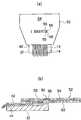
도 1은 본 발명에 따른 프로브 카드의 사시도이다.
도 2는 도 1에 도시한 프로브 카드의 측면도이다.
도 3은 본 발명에 따른 프로브 조립체 및 프로브 카드의 제조에 사용되는 프로브의 사시도이다.
도 4는 본 발명에 따른 프로브 조립체의 제조에 사용되는 지그의 사시도이다.
도 5의 (a), (b) 및 (c)는 각각 지그의 복수 개의 홈에 각각 배치된 복수 개의 프로브를 도시한 평면도, 종단면도 및 측면도이다.
도 6의 (a), (b) 및 (c)는 각각 지그의 표면 및 복수 개의 프로브가 피복층으로 덮인 상태를 도시한 평면도, 종단면도 및 측면도이다.
도 7의 (a), (b) 및 (c)는 각각 복수 개의 프로브의 베이스 단부가 규정하는 평탄면이 노출된 상태를 도시한 평면도, 종단면도 및 측면도이다.
도 8의 (a), (b) 및 (c)는 각각 평탄면에 기재가 접합된 상태를 도시한 평면도, 종단면도 및 측면도이다.
도 9의 (a) 및 (b)는 각각 기재에 관통홀이 설치된 상태를 도시한 평면도 및 종단면도이다.
도 10은 기재의 관통홀에 도전성 재료가 채워진 상태를 도시한 종단면도이다.
도 11의 (a), (b) 및 (c)는 각각 기재의 타측 면 상에 도전성 피막이 형성된 상태를 도시한 평면도, 종단면도 및 측면도이다.
도 12의 (a), (b) 및 (c)는 각각 피복층 및 지그를 제거한 후에 남는 본 발명에 따른 프로브 조립체의 평면도, 종단면도 및 측면도이다.
도 13은 본 발명에 따른, 제조 도중에 있는 다른 프로브 조립체에 대한 도 11(a)에 도시한 것과 동일한 상태를 도시한 평면도이다.
도 14의 (a), (b) 및 (c)는 각각 제1 기재 상에 제2 기재가 접합된 상태를 도시한 평면도, 종단면도 및 측면도이다.
도 15의 (a) 및 (b)는 각각 제2 기재에 관통홀이 설치된 상태를 도시한 평면도 및 종단면도이다.
도 16의 (a) 및 (b)는 각각 제2 기재의 관통홀에 도전성 재료가 채워진 상태를 도시한 평면도 및 종단면도이다.
도 17의 (a) 및 (b)는 각각 제2 기재의 타측 면 상에 도전성 피막이 형성된 상태를 도시한 평면도 및 종단면도이다.
도 18의 (a) 및 (b)는 각각 피복층 및 지그을 제거한 후에 남는 본 발명에 따른 다른 프로브 조립체의 평면도 및 종단면도이다.1 is a perspective view of a probe card according to the present invention.
2 is a side view of the probe card shown in Fig.
3 is a perspective view of a probe used in the manufacture of the probe assembly and the probe card according to the present invention.
4 is a perspective view of a jig used in the manufacture of a probe assembly according to the present invention.
5 (a), 5 (b) and 5 (c) are a plan view, a longitudinal sectional view, and a side view, respectively, of a plurality of probes respectively arranged in a plurality of grooves of a jig.
6 (a), 6 (b) and 6 (c) are a plan view, a vertical sectional view, and a side view, respectively, showing a surface of a jig and a plurality of probes covered with a coating layer.
7 (a), 7 (b) and 7 (c) are a plan view, a longitudinal sectional view and a side view, respectively, showing a state in which a flat surface defined by base ends of a plurality of probes are exposed.
8 (a), 8 (b) and 8 (c) are a plan view, a vertical sectional view, and a side view, respectively, showing a state in which a base material is bonded to a flat surface.
9 (a) and 9 (b) are a plan view and a longitudinal sectional view showing a state in which a through hole is formed in a substrate, respectively.
10 is a longitudinal sectional view showing a state in which a through hole of a substrate is filled with a conductive material.
11 (a), 11 (b) and 11 (c) are a plan view, a longitudinal sectional view and a side view, respectively, showing a state in which a conductive film is formed on the other side of the substrate.
12 (a), 12 (b) and 12 (c) are a plan view, a longitudinal sectional view and a side view, respectively, of a probe assembly according to the present invention, which remains after removing the coating layer and the jig.
Fig. 13 is a plan view showing the same state as that shown in Fig. 11 (a) for another probe assembly in the middle of manufacturing according to the present invention. Fig.
14 (a), 14 (b) and 14 (c) are a plan view, a vertical sectional view and a side view, respectively, showing a state in which the second base material is bonded to the first base material.
15 (a) and 15 (b) are a plan view and a longitudinal sectional view showing a state in which a through hole is provided in the second substrate, respectively.
16 (a) and 16 (b) are a plan view and a longitudinal sectional view showing a state in which a conductive material is filled in the through-hole of the second substrate.
17 (a) and 17 (b) are a plan view and a longitudinal sectional view, respectively, showing a state in which a conductive film is formed on the other side of the second substrate.
18 (a) and 18 (b) are a plan view and a longitudinal sectional view, respectively, of another probe assembly according to the present invention, which remains after removing the coating layer and the jig.
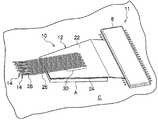
도 1 및 도 2를 참조하면, 본 발명에 따른 프로브 조립체 및 프로브 카드가 각각 전체에 부호 10 및 11로 도시되어 있다.1 and 2, a probe assembly and a probe card according to the present invention are shown generally at 10 and 11, respectively.
프로브 조립체(10)는, 전기 절연성을 갖는 기재(12)와, 캔틸레버 프로브라고 칭해질 수 있는 금속으로 된 복수 개의 프로브(14)와, 기재(12)에 설치되며 도전성 재료(16)로 채워진, 프로브(14)와 같은 수의 관통홀(18)(도 12(b))과, 기재(12)에 설치된, 프로브(14)와 같은 수의 도전성 피막(20)(도 12(a) 내지 (c))을 포함한다.The
프로브 카드(11)는, 기판(C)과, 상기 기판에 부착된 프로브 조립체(10)로 이루어진다. 프로브 조립체(10)는, 이를 구성하는 기재(12)의 후기(後記) 면(24)이 기판(C)에 대향하도록 배치되어 있다. 보다 상세하게는, 프로브 조립체(10)는 그 기재(12)에 있어서 누름 금구(B)를 통하여 기판(C)에 고정되고, 또한, 기재(12)와 기판(C)과의 사이에 배치된 플랫폼(A)을 통하여 기판(C)에 고정 장착되어 있다. 여기서 프로브 조립체(10)의 복수 개의 도전성 피막(20)이 이들의 선단에 형성된 범프(46)(도 12(a))에 있어서, 각각, 기판(C)에 형성된, 범프(46)와 같은 수의 복수 개의 랜드(도시하지 않음)에 접촉해 있다.The
프로브 조립체(10)의 기재(12)는 플렉시블 프린트 배선 기판과 같은 판체로 이루어지며, 서로 대향하는 2개의 면(평탄면)(22, 24)을 갖는다. 기재(12)는, 도시한 예에서는 사다리꼴의 평면 형상을 갖는 사다리꼴 부분과 상기 사다리꼴 부분에 연속되는, 직사각형의 평면 형상을 갖는 직사각형 부분으로 이루어진다. 기재(12)는, 도시한 예 대신, 상기 평면 형상 이외의 임의의 평면 형상을 갖는 것으로 할 수 있다. 또한, 도 1을 참조하여 설명한 플랫폼(A)은 기재(12)의 면(24)의 측에 있어서 상기 사다리꼴 부분 상에 위치하고, 또한, 누름 금구(B)는 기재(12)의 면(22)의 측에 있어서 상기 직사각형 부분 상에 위치한다. 플랫폼(A)은, 바람직하게는 프로브(14)보다 열팽창률이 낮은 것이 선택된다.The
복수 개의 프로브(14)는, 각각 기재(12)의 일측 면(22) 상에 서로 간격을 두고 평행하게 배치되고, 또한 기재(12)에 지지되어 있다. 각 프로브(14)는 도 1 및 도 2에 더하여 도 3에 추가로 도시한 바와 같이, 가늘고 긴 본체(26)와, 상기 본체의 일단부 및 타단부에 각각 연속되는 침선부(28) 및 베이스 단부(30)를 갖는다.The plurality of
각 프로브(14)의 침선부(28)는 본체(26)의 일단부로부터 이와 각도를 이루어 끝이 가늘어지게 뻗으며, 베이스 단부(30)는 본체(26)의 타단부에 고정된 직사각 형상의 판체로 이루어진다. 또한, 각 프로브(14)의 베이스 단부(30)는, 기재(12)의 일측 면(22)에 접착된 평탄한 접합면(31)을 갖는다(도 2 참조). 이것에 의해, 각 프로브(14)는 그 베이스 단부(30)를 통하여, 그 가늘고 긴 본체(26)와 침선부(28)가 기재(12)의 일측 면(22)과의 사이에 빈틈이 있는 상태로, 즉 외팔보 상태로 기재(12)에 지지되어 있다. 외팔보 지지된 각 프로브(14)는, 그 침선부(28)에 있어서, 기능 테스트를 위해 피검사체(반도체 집적 회로)의 전극에 압박될 때, 그 본체(26)에 있어서 휘는 것이 가능하다.The
도시한 복수 개의 프로브(14)는, 이들 본체(26)가 기재(12)의 일측 면(22)에 대해 이것과 평행하게 뻗도록 배치되어 있다. 이 대신, 본체(26)가 기재(12)의 일측 면(22)에 대해 이것과 각도를 이루어 뻗도록, 예컨대 상기 각도가 베이스 단부(30)로부터 침선부(28)를 향해 점진적으로 증가하도록 배치하는 것이 가능하다. 또한, 도시한 복수 개의 프로브(14)는 서로 평행하게 그리고 이들 침선부(28)가 가지런해지지 않도록 배열되어 있는데, 이 배열은 상기 피검사체의 전극의 배치 위치에 따라 결정된다. 따라서, 프로브(14)의 배열은 도시한 예에 한정되지 않는다.The illustrated plurality of
도 12(b)에 도시한 바와 같이, 기재(12)에 설치되며 그 양면(22, 24)에 개방하는 각 관통홀(18)을 채우는 도전성 재료(16)는, 기재(12)의 일측 면(22)의 측에 있어서 각 프로브(14)의 일부인 베이스부(30), 보다 상세하게는 베이스부(30)의 접합면(31)에 접착되어 있다. 또한, 기재(12)에 설치된 각 도전성 피막(20)은, 기재(12)의 타측 면(24) 상을 각 프로브(14)와 반대 방향으로 뻗으며 기재(12)의 타측 면(24)의 측에 있어서 각 관통홀(18)을 채우는 도전성 재료(16)에 접착되어 있다. 이에 따라, 각 프로브(14)와 상기 프로브에 대응하는 각 도전성 피막(20)이 각 관통홀(18) 중의 도전성 재료(16)를 통하여 전기적으로 접속되어 있다.The
각 관통홀(18) 속으로의 도전성 재료(16)의 충전 및 도전성 피막(20)의 형성 및 도전성 재료(16)와 각 프로브(14) 및 각 도전성 피막(20)과의 접착은 후술하는 본 발명에 따른 제조 방법을 이용하여 인력에 의하지 않고 기계적으로 수행하는 것이 가능하다. 각 관통홀(18)을 채우는 도전성 재료(16)와 각 프로브(14) 및 각 도전성 피막(배선)(20)과의 상호 접착의 구조는 프로브 조립체(10)에 있어서 각 프로브(14)와 각 도전성 피막(16)과의 접속부의 품질의 향상을 가져온다. 또한, 각 프로브(14)와 각 도전성 피막(16)과의 접속부의 형성에 소요되는 시간의 단축도 가능하게 하며, 나아가 이들 사이의 오접속을 없앤다.Filling of the
다음, 본 발명에 따른 프로브 조립체(10)의 제조 방법에 대해 설명한다.Next, a method of manufacturing the
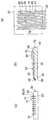
먼저, 도 4에 도시한 바와 같은 지그(32)를 준비한다. 지그(32)는, 표면(34)과, 서로 등간격으로 배치되며 표면(34)에 개방하는, 복수 개의 프로브(14)와 같은 수의 홈(36)을 갖는다. 지그(32)는, 프로브 조립체(10)의 제조를 위해 복수 개의 프로브(14)를 각각 복수 개의 홈(36)에 수용하고, 정렬한 상태로 홀딩하는 기능을 담당한다.First, a
지그(32)는, 예컨대 직육면체 형상을 이루는 세라믹으로 된 블록으로 이루어지며, 서로 직교하는 평탄한 6개의 면을 갖는다. 상기 블록은 그 표면(34)에 연속되는, 서로 대향하는 평탄한 두 측면(38, 40)을 갖는다. 지그(32)는 다른 형상 또는 다른 재료로 이루어지는 것으로 할 수 있다. 또한, 지그의 표면(34)은, 도시한 예 대신, 만곡면이나 요철면으로 이루어지는 것일 수도 있다.The
복수 개의 홈(36)은, 지그(32)의 표면(34) 상을 상기 지그의 일측의 측면(38)으로부터 타측의 측면(40)을 향해 서로 평행하게 뻗으며, 타측의 측면(40)에 이르기 바로 앞의 위치에서 종단해 있다. 이 예 대신, 각 홈(36)은, 표면(34)에만 개방하는 것으로 할 수 있다.The plurality of
각 홈(36)은, 각 프로브(14)가 각 홈(36)을 따라 뻗으며 각 프로브(14)의 베이스 단부(30)가 각 홈(36)의 외부에 있도록 수용 가능한 치수를 갖는다. 도시한 예에서는, 각 홈(36)은 각 프로브(14)의 길이 치수보다 작은 길이 치수, 보다 상세하게는 대략 침선부(28)를 제외한 길이 치수와, 각 프로브(14)의 본체(26)의 높이 치수(도 2에서 보아 상하 방향에서의 치수)와 대략 동일한 깊이 치수 및 본체(26)의 폭 치수(도 2에서 보아 종이 뒷면 방향에서의 치수)보다 약간 큰 폭 치수를 갖는다. 이에 따르면, 각 프로브(14)가 각 홈(36)에 배치될 때(도 5(a) 내지 (c) 참조), 그 침선부(28) 및 그에 연속되는 본체(26)의 일부분이 각 홈(36)을 그 일단 즉 지그(32)의 측면(38)으로부터 돌출하고, 또한, 그 베이스 단부(30)의 일부분이 지그(32)의 표면(34)의 상방으로 돌출한다.Each
또한, 복수 개의 홈(36)의 타단은 교대로 가지런하지 않도록, 즉, 서로 인접하는 2개의 홈(36)의 타단과 지그(32)의 타측의 측면(40)과의 사이의 거리(a 및 b)가 각각 a>b의 관계가 되도록 설정되어 있다. 따라서, 서로 인접하는 2개의 홈(36) 중 하나의 홈은 그 다른 홈보다 긴(또는 짧은) 길이 치수를 갖는다. 거리(a) 및 거리(b)의 차(a-b)는, 도 1에서 보아, 서로 인접하는 2개의 프로브(14)의 침선부(28)의 자유단 상호의 상기 프로브의 길이 방향에서의 차와 같다.The distance a between the other end of the two
지그(32)는, 상기한 바와 같이, 복수 개의 프로브(14)를 서로 정렬한 상태로 홀딩하는 작용을 이루며, 최종적으로 이들 프로브(14)로부터 분리된다. 이 관점에서는, 지그(32)의 각 홈(36)은 그 일단이 지그(32)의 일측의 측면(38)에 개방하지 않는 것, 즉 각 프로브(14)의 전체 길이를 수용 가능한 길이 치수를 갖는 것으로 하고, 혹은 이에 더하여, 각 프로브(14)의 베이스 단부(30)의 전부를 수용 가능한 깊이 치수를 갖는 것으로 하는 것이 가능하다.As described above, the
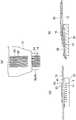
다음, 도 5(a), (b) 및 (c)에 도시한 바와 같이, 지그(32)의 복수 개의 홈(36)에 복수 개의 프로브(14)를 배치한다. 그 결과, 그 침선부(28) 및 그에 연속되는 본체(26)의 일부분이 각 홈(36)의 상기 일단으로부터 돌출하고, 그 베이스 단부(30)의 일부분이 각 홈(36)으로부터 지그(32)의 표면(34)의 상방으로 돌출한다.Next, as shown in Figs. 5 (a), (b) and (c), a plurality of
다음, 도 6(a), (b) 및 (c)에 도시한 바와 같이, 지그(32)의 표면(34) 상에 상기 표면과 복수 개의 프로브(14)를 덮는 피복층(42)을 형성한다.Next, a
피복층(42)의 형성에 의해, 홈(36) 내의 모든 프로브(14)가 지그(32)의 표면(34)에 고정되고, 모든 프로브(14)의 정렬 상태가 유지된다. 피복층(42)은, 예컨대 공지의 전기 도금 기술을 이용하여 얻어지는 도금층, 바람직하게는 구리의 도금층으로 이루어진다.All the
피복층(42)의 형성후, 피복층(42)의 일부와 복수 개의 프로브(14)의 베이스 단부(30)의 일부분를 제거하고, 지그(32)의 표면(34)과 평행한 평탄면(44)을 형성한다. 평탄면(44)은, 각 베이스 단부(30)의 일부분의 제거에 의해 생긴 상기 베이스 단부의 노출면을 포함한다. 상기 노출면은, 도 2를 참조하여 설명한 복수 개의 프로브(14)의 베이스 단부(30)의 접합면(31)을 이룬다(도 7(a), (b) 및 (c) 참조). 이 예 대신, 베이스 단부(30)가 나타날 때까지 피복층(42)의 일부를 제거함으로써 상기 평탄면을 형성할 수도 있다.After forming the
평탄면(44)의 형성은, 예컨대 평면 연삭기의 연삭기 바이트(46)(도 6(b))를 화살표(48)의 방향으로 이동시키고, 피복층(42)과 상기 피복층의 내부의 베이스 단부(30)에 연삭 가공을 실시함으로써 수행할 수 있다.The
그 후, 도 8(a), (b) 및 (c)에 도시한 바와 같이, 형성된 평탄면(44) 상에 전기 절연성의 기재(12)를 올리고, 그 일측 면(22)에 있어서 평탄면(44)에 접착한다. 이에 따라, 복수의 프로브(14)의 베이스 단부(30)의 접합면(31)이 기재(12)에 의해 덮인다.Thereafter, as shown in Figs. 8 (a), 8 (b) and 8 (c), an electrically insulating
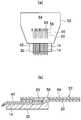
다음, 도 9(a) 및 (b)에 도시한 바와 같이, 기재(12)에, 복수 개의 프로브(14)의 베이스 단부(30)에 각각 대응하며 또한 대향하는 복수 개의 관통홀(18)을 설치한다. 각 관통홀(18)은, 기재(12)의 일측 면(22) 및 타측 면(24)에 개방해 있다. 기재(12)의 일측 면(22)에 개방하는 각 관통홀(18)의 단면(端面)은, 각 프로브(14)의 베이스 단부(30)의 접합면(31)에 의해 폐쇄되고, 접합면(31)이 폐쇄 단면면을 규정한다. 관통홀(18)은, 예컨대 공지의 엑시머 레이저 가공기(도시하지 않음)를 이용한 구멍뚫기 가공에 의해 설치할 수 있다.Next, as shown in Figs. 9 (a) and 9 (b), a plurality of through
이어서, 도 10에 도시한 바와 같이, 기재(12)에 설치된 각 관통홀(18)을 도전성 재료(16)로 채운다. 도전성 재료(16)는, 예컨대 공지의 전기 도금 기술을 이용하여 얻어지는 도금층, 바람직하게는 구리의 도금층으로 이루어지는 것으로 할 수 있다.Then, as shown in Fig. 10, the through
각 관통홀(18)이 도전성 재료(16)로 채워질 때, 각 프로브(14)의 베이스 단부(30)의 접합면(31)이 각 관통홀(18)의 상기 폐쇄 단면을 규정하고 있으므로, 도전성 재료(16)가 접합면(31)에 접하고, 여기에 접착된다.Since the connecting
각 관통홀(18)에 대한 도전성 재료(16)의 충전 후, 기재(12)의 타측 면(24) 상에, 각 관통홀(18) 내의 도전성 재료(16)에 접착하는 도전성 피막(20)을 형성한다. 이들 도전성 피막(20)은 배선 패턴을 이룬다(도 11(a), (b) 및 (c)).A
그 후, 피복층(42)을 제거하고, 이어서 지그(32)를 철거한다. 피복층(42)의 제거는, 피복층(42)이 상기 구리의 도금층으로 이루어질 때에는, 구리의 선택 에칭액을 이용한 에칭에 의해 수행할 수 있다. 피복층(42)의 제거에 의해 피복층(42)에 접착되어 있던 지그(32)를 개방할 수 있고, 이에 따라 철거할 수 있다.Thereafter, the
피복층(42)의 제거 및 지그(32)의 철거에 의해 각 관통홀(18) 내의 도전성 재료(16)를 각 프로브(14)와 각 도전성 피막(20)과의 접속부로 하는 본 발명에 따른 프로브 조립체(10)를 얻을 수 있다.A probe according to the present invention in which the
그런데, 얻어진 프로브 조립체(10)는, 상기 피검사체의 각 전극에 대응하는 각 도전성 피막(20)의 선단부(범프)(46)의 상호 간격이 비교적 좁은 것으로 이루어진다. 이에 반해, 본 발명의 다른 프로브 조립체(50)(도 18 (a) 참조) 및 이를 포함하는 프로브 카드(도시하지 않음)에서는 상기 상호 간격이 보다 넓은 것으로 되어 있다.The obtained
프로브 조립체(50)는, 도 5 내지 도 12 및 도 13 내지 도 18에 도시한 공정을 통해 제조할 수 있다.The
프로브 조립체(50)는, 도 18 (b)에 도시한 바와 같이, 프로브 조립체(10)와, 여기에 겹쳐 배치된 후기 다른 기재(52)를 포함한다. 프로브 조립체(10)는, 상기한 바와 같이, 서로 대향하는 2개의 면(22, 24)을 갖는 전기 절연성의 기재(제1 기재)(12)와, 복수 개의 프로브(14)와, 도전성 재료(16)가 채워지며, 상기 도전성 재료가 각 프로브에 접착된 각 관통홀(제1 관통홀)(18)과, 제1 기재(12)의 타측 면 상에 형성되며 또한 복수 개의 제1 관통홀(18)의 도전성 재료(16)에 각각 접착된 복수 개의 도전 피막(제1 도전성 피막)(20)을 포함한다. 다른 프로브 조립체(50)는, 추가로, 서로 대향하는 2개의 면(62, 64)을 갖는 전기 절연성의 제2 기재(52)로서 그 일면(62)이 제1 기재(12)를 향하게 하여 상기 제1 기재 상에 포개진 제2 기재(52)와, 상기 제2 기재에 복수 개의 제1 도전성 피막(20)에 각각 대응하여 설치되며 도전성 재료(56)로 채워진 복수 개의 제2 관통홀(58)로서, 각 제2 관통홀(58)의 도전성 재료(56)가 각 제1 도전성 피막(20)에 접착된 복수 개의 제2 관통홀(58)과, 제2 기재(52)의 다른 면(64) 상에 형성되며 복수 개의 제2 관통홀(58)의 도전성 재료(56)에 각각 접착된 복수 개의 제2 도전성 피막(60)을 포함한다. 복수 개의 제2 도전성 피막(60)은 각각 상기 피검사체의 복수 개의 전극에 대응하는 단부(端部)(범프)(66)를 갖는다.The
프로브 조립체(50)의 제조를 위해, 먼저, 도 5 내지 도 12에 도시한 공정을 통해 상기한 바와 동일한 프로브 조립체(10)(도 13)를 제조한다. 도 13에 도시한 프로브 조립체(10)는, 복수 개의 제1 도전성 피막(20) 중 하나(도 13에서 보아 왼쪽 끝에 위치하는 하나)가 갈고리 형태로 뻗는 점에 있어서, 모든 도전성 피막(20)이 직선형으로 뻗는 도 12에 도시한 프로브 조립체(10)와 다르다. 이는, 좌우 배선 교체를 위해, 즉, (도 13에서 보아) 왼쪽 끝에 위치하는 제1 도전성 피막이 (도 18(a)에서 보아) 오른쪽 끝을 향해 뻗는 제2 도전성 피막(60)에 연속되고, (도 13에서 보아) 오른쪽 끝에 위치하는 제1 도전성 피막(20)이 (도 18에서 보아) 왼쪽 끝을 향해 뻗는 제2 도전성 피막(60)에 연속되도록 하기 위한 조치이다.For the manufacture of the
다음, 도 14(a), (b) 및 (c)에 도시한 바와 같이, 제1 도전성 피막(20)이 형성된 제1 기재(12) 상에 전기 절연성의 제2 기재(52)를 올리고, 그 일측 면(62)에 있어서 제1 기재(12)에 접착한다. 이에 따라, 복수 개의 제1 도전성 피막(20)이 제2 기재(52)에 의해 덮인다. 여기서, 미리 제1 기재(12)의 면(24)에 제1 도전성 피막(20)을 제외하고 필름(예컨대 드라이 필름, 폴리이미드 필름 등)(68)을 붙여 면(24)을 덮어 둘 수 있다. 이에 따라, 면(24)과 제1 도전성 피막(20)이 형성하는 요철면을 비교적 평탄한 것으로 할 수 있다. 또한, 이에 따라, 절연성이나 인덕턴스와 같은 전기적 특성을 향상시킬 수 있다. 필름(68)을 사용할 때에는 제2 기재(52)는 면(24)을 덮는 필름(68)에 접착된다.Next, as shown in Figs. 14A, 14B and 14C, the electrically insulating
다음, 도 15(a) 및 (b)에 도시한 바와 같이, 제2 기재(52)에, 복수 개의 제1 도전성 피막(20)에 각각 대응하며 또한 대향하는 복수 개의 제2 관통홀(58)을 설치한다. 각 제2 관통홀(58)은, 제2 기재(52)의 일측 면(62) 및 타측 면(64)에 개방해 있다. 제2 기재(52)의 일측 면(62)에 개방하는 각 제2 관통홀(58)의 단면은 각 제1 도전성 피막(20)에 의해 폐쇄되고, 상기 제1 도전성 피막이 폐쇄 단면을 규정한다. 제2 관통홀(58)은, 제1 관통홀(18)과 동일하게, 예컨대 공지의 엑시머 레이저 가공기(도시하지 않음)를 이용한 구멍뚫기 가공에 의해 설치할 수 있다.Next, as shown in Figs. 15 (a) and 15 (b), the
이어서, 도 16(a) 및 (b)에 도시한 바와 같이, 제2 기재(52)에 설치된 각 제2 관통홀(58)을 제2 도전성 재료(56)로 채운다. 제2 도전성 재료(56)는, 제1 도전성 재료(16)와 마찬가지로, 예컨대 공지의 전기 도금 기술을 이용하여 얻어지는 도금층, 바람직하게는 구리의 도금층으로 이루어지는 것으로 할 수 있다.Then, as shown in Figs. 16A and 16B, the second through
각 제2 관통홀(58)이 제2 도전성 재료(56)로 채워질 때, 각 제1 도전성 피막(20)이 각 제2 관통홀(58)의 상기 폐쇄 단면을 규정하고 있으므로, 제2 도전성 재료(56)가 제1 도전성 피막(20)에 접하고, 여기에 접착한다.Since each first
각 제2 관통홀(58)에 대한 제2 도전성 재료(56)의 충전 후, 제2 기재(52)의 타측 면(64) 상에, 각 제2 관통홀(58) 내의 제2 도전성 재료(56)에 접착하는 제2 도전성 피막(60)을 형성한다. 이들 제2 도전성 피막(60)은 배선 패턴을 이룬다(도 17(a) 및 (b)).The second
그 후, 피복층(42)을 제거하고, 이어서 지그(32)를 철거한다(도 18(a) 및 (b)). 피복층(42)의 제거는, 상기한 바와 동일하게, 피복층(42)이 상기 구리의 도금층으로 이루어질 때에는, 구리의 선택 에칭액을 이용한 에칭에 의해 수행할 수 있다. 피복층(42)의 제거에 의해 피복층(42)에 접착되어 있던 지그(32)를 개방할 수 있고, 이에 따라 철거할 수 있다.Thereafter, the
피복층(42)의 제거 및 지그(32)의 철거에 의해, 각 제1 관통홀(18) 내의 도전성 재료(16)를 각 프로브(14)와 각 제1 도전성 피막(20)과의 접속부로 하고, 또한, 각 제2 관통홀(58) 내의 도전성 재료(56)를 각 제1 도전성 피막(20)과 각 제2 도전성 피막(60)과의 접속부로 하는 프로브 조립체(50)를 얻을 수 있다.The
프로브 조립체(50)를 포함하는 프로브 카드(도시하지 않음)는, 상기한 프로브 조립체(10)를 포함하는 상기 프로브 카드에서와 동일하게, 기판(C)에 프로브 조립체(50)를 부착하여 이루어진다. 프로브 조립체(50)는, 이를 구성하는 제2 기재(52)의 타측 면(64)이 기판(C)에 대향하도록 배치된다. 보다 상세하게는, 프로브 조립체(50)는 그 제1 및 제2의 두 기재(12, 52)에 있어서 누름 금구(B)를 통하여 기판(C)에 고정되고, 또한 제2 기재(52)와 기판(C)과의 사이에 배치된 플랫폼(A)을 통하여 기판(C)에 고정 장착된다. 여기서, 마찬가지로, 프로브 조립체(50)의 복수 개의 제2 도전성 피막(60)이 이들의 선단에 형성된 범프(66)에 있어서, 각각 기판(C)에 형성된, 범프(66)와 같은 수의 복수 개의 랜드(도시하지 않음)에 접촉해 있다.A probe card (not shown) including the
10, 50…프로브 조립체
12, 52…기재
14…프로브
16, 56…도전성 재료
18, 58…관통홀
20, 60…도전성 피막
22, 62…기재의 일측 면
24, 64…기재의 타측 면
26, 28, 30…프로브의 본체, 침선부 및 베이스 단부
31…베이스 단부의 접합면
32…지그
34…지그의 표면
36…홈
42…피복층
44…평탄면10, 50 ... Probe assembly
12, 52 ... materials
14 ... Probe
16, 56 ... Conductive material
18, 58 ... Through hole
20, 60 ... Conductive film
22, 62 ... One side of the substrate
24, 64 ... The other side of the substrate
26, 28, 30 ... The body of the probe, the needle bar portion and the base end
31 ... The joint surface of the base end
32 ... Jig
34 ... Surface of jig
36 ... home
42 ... Coating layer
44 ... Flat face
Claims (10)
Translated fromKorean베이스 단부를 갖는 복수 개의 프로브를, 각 프로브가 각 홈을 따라 뻗으며 각 프로브의 베이스 단부의 일부분이 각 홈 바깥에 있도록 상기 지그의 복수 개의 홈 내에 각각 배치하는 것,
상기 지그의 표면 상에 상기 표면과 상기 프로브를 덮는 피복층을 형성하는 것,
상기 프로브의 베이스 단부가 노출되는 상기 지그의 표면과 평행한 노출면을 형성하기 위해, 상기 피복층의 일부 또는 상기 피복층의 일부에 더하여 상기 프로브의 베이스 단부의 일부분을 제거하는 것,
상기 노출면에, 서로 대향하는 2개의 면을 갖는 전기 절연성의 기재를 그 일측 면에 있어서 접착하는 것,
상기 기재에, 각 프로브의 베이스 단부에 대향하는 관통홀을 설치하는 것,
각 관통홀을 도전성 재료로 채우는 것,
상기 기재의 타측 면 상에, 각 관통홀 내의 도전성 재료에 접착하는 도전성 피막을 형성하는 것,
상기 피복층을 제거하는 것,
상기 지그를 철거하는 것을 포함하는 프로브 조립체의 제조 방법.Preparing a jig having a surface and a plurality of grooves opening on the surface,
Placing a plurality of probes having a base end in respective ones of the plurality of grooves of the jig such that each probe extends along each groove and a portion of the base end of each probe is outside each groove,
Forming a coating layer covering the surface and the probe on the surface of the jig,
Removing a portion of the base end of the probe in addition to a portion of the coating layer or a portion of the coating layer to form an exposed surface parallel to the surface of the jig to which the base end of the probe is exposed;
An electrically insulating substrate having two faces opposite to each other is bonded to the exposed surface on one side thereof,
It is possible to provide a penetrating hole opposed to the base end of each probe on the substrate,
Filling each through hole with a conductive material,
Forming a conductive film to be adhered to the conductive material in each of the through holes on the other side of the substrate,
Removing the coating layer,
And removing the jig.
베이스 단부를 갖는 복수 개의 프로브를, 각 프로브가 각 홈을 따라 뻗으며 각 프로브의 베이스 단부의 일부분이 각 홈 바깥에 있도록 상기 지그의 복수 개의 홈 내에 각각 배치하는 것,
상기 지그의 표면 상에 상기 표면과 상기 프로브를 덮는 피복층을 형성하는 것,
상기 프로브의 베이스 단부가 노출되는 상기 지그의 표면과 평행한 노출면을 형성하기 위해, 상기 피복층의 일부 또는 상기 피복층의 일부에 더하여 상기 프로브의 베이스 단부의 일부분을 제거하는 것,
상기 노출면에, 서로 대향하는 2개의 면을 갖는 전기 절연성의 제1 기재를 그 일측 면에 있어서 접착하는 것,
상기 제1 기재에, 각 프로브의 베이스 단부에 대향하는 제1 관통홀을 설치하는 것,
상기 제1 기재에 설치된 각 제1 관통홀을 도전성 재료로 채우는 것,
상기 제1 기재의 타측 면 상에, 각 제1 관통홀 내의 도전성 재료에 접착하는 제1 도전성 피막을 형성하는 것,
상기 제1 기재 상에, 서로 대향하는 2개의 면을 갖는 전기 절연성의 제2 기재를 그 일면이 상기 제1 기재의 다른 면을 향하게 하여 포개는 것,
상기 제2 기재에, 각 제1 도전성 피막에 대향하는 제2 관통홀을 설치하는 것,
상기 제2 기재에 설치된 각 제2 관통홀을 도전성 재료로 채우는 것,
상기 제2 기재의 타측 면 상에, 각 제2 관통홀 내의 도전성 재료에 접착하는 제2 도전성 피막을 형성하는 것,
상기 피복층을 제거하는 것,
상기 지그를 철거하는 것을 포함하는 프로브 조립체의 제조 방법.Preparing a jig having a surface and a plurality of grooves opening on the surface,
Placing a plurality of probes having a base end in respective ones of the plurality of grooves of the jig such that each probe extends along each groove and a portion of the base end of each probe is outside each groove,
Forming a coating layer covering the surface and the probe on the surface of the jig,
Removing a portion of the base end of the probe in addition to a portion of the coating layer or a portion of the coating layer to form an exposed surface parallel to the surface of the jig to which the base end of the probe is exposed;
Bonding the first electrically-insulating base material having two surfaces opposed to each other on the exposed surface,
Providing a first through hole opposed to the base end of each probe on the first base,
Filling each of the first through holes provided in the first base material with a conductive material,
Forming a first conductive film to be adhered to the conductive material in each of the first through holes on the other side of the first base material;
An electrically insulating second base material having two surfaces opposed to each other on the first base material, the one surface of the second base material facing the other surface of the first base material,
Providing a second through hole opposed to each of the first conductive coatings on the second base,
Filling each of the second through holes provided in the second substrate with a conductive material,
Forming a second conductive film to be adhered to the conductive material in each of the second through holes on the other side of the second substrate,
Removing the coating layer,
And removing the jig.
Applications Claiming Priority (2)
| Application Number | Priority Date | Filing Date | Title |
|---|---|---|---|
| JPJP-P-2011-278018 | 2011-12-20 | ||
| JP2011278018AJP2013130400A (en) | 2011-12-20 | 2011-12-20 | Probe assembly, probe card including the same and manufacturing method thereof |
Publications (2)
| Publication Number | Publication Date |
|---|---|
| KR20130071363A KR20130071363A (en) | 2013-06-28 |
| KR101399030B1true KR101399030B1 (en) | 2014-05-30 |
Family
ID=48609504
Family Applications (1)
| Application Number | Title | Priority Date | Filing Date |
|---|---|---|---|
| KR1020120140973AActiveKR101399030B1 (en) | 2011-12-20 | 2012-12-06 | Probe Assembly, Probe Card Including the Same, and Methods for Manufacturing These |
Country Status (4)
| Country | Link |
|---|---|
| US (1) | US9121869B2 (en) |
| JP (1) | JP2013130400A (en) |
| KR (1) | KR101399030B1 (en) |
| TW (1) | TWI491886B (en) |
Families Citing this family (7)
| Publication number | Priority date | Publication date | Assignee | Title |
|---|---|---|---|---|
| KR101646771B1 (en)* | 2015-01-27 | 2016-08-08 | 한국기술교육대학교 산학협력단 | A probe pin manufacturing method using a jig |
| TWI572868B (en)* | 2015-07-03 | 2017-03-01 | Mpi Corp | Detection device and its probe module |
| KR101849988B1 (en) | 2018-01-17 | 2018-04-18 | 주식회사 제다온 | Probe assembly for display panel inspection |
| CN111141938B (en)* | 2018-11-02 | 2021-10-29 | 旺矽科技股份有限公司 | Probe module for multiple units under test with inclined conductive contacts |
| JP2020134216A (en)* | 2019-02-15 | 2020-08-31 | 株式会社サンケイエンジニアリング | Inspection jig |
| JP7292921B2 (en)* | 2019-03-29 | 2023-06-19 | 株式会社日本マイクロニクス | Multi-pin structure probe body and probe card |
| TWI704355B (en)* | 2019-07-22 | 2020-09-11 | 旺矽科技股份有限公司 | Suitable for probe modules with multiple units to be tested with inclined conductive contacts |
Citations (4)
| Publication number | Priority date | Publication date | Assignee | Title |
|---|---|---|---|---|
| JP2001153885A (en) | 1999-11-26 | 2001-06-08 | Micronics Japan Co Ltd | Probe card |
| JP2007285801A (en)* | 2006-04-14 | 2007-11-01 | Micronics Japan Co Ltd | Probe seat and electrical connection device |
| JP2007285802A (en) | 2006-04-14 | 2007-11-01 | Micronics Japan Co Ltd | Probe sheet manufacturing method |
| KR20100137240A (en)* | 2009-06-22 | 2010-12-30 | (주)티에스이 | Probe assembly for accurate soldering |
Family Cites Families (2)
| Publication number | Priority date | Publication date | Assignee | Title |
|---|---|---|---|---|
| JP3781480B2 (en)* | 1996-06-10 | 2006-05-31 | 株式会社日本マイクロニクス | Probe card |
| JP4902248B2 (en)* | 2006-04-07 | 2012-03-21 | 株式会社日本マイクロニクス | Electrical connection device |
- 2011
- 2011-12-20JPJP2011278018Apatent/JP2013130400A/enactivePending
- 2012
- 2012-12-06KRKR1020120140973Apatent/KR101399030B1/enactiveActive
- 2012-12-17TWTW101147767Apatent/TWI491886B/enactive
- 2012-12-18USUS13/719,161patent/US9121869B2/enactiveActive
Patent Citations (4)
| Publication number | Priority date | Publication date | Assignee | Title |
|---|---|---|---|---|
| JP2001153885A (en) | 1999-11-26 | 2001-06-08 | Micronics Japan Co Ltd | Probe card |
| JP2007285801A (en)* | 2006-04-14 | 2007-11-01 | Micronics Japan Co Ltd | Probe seat and electrical connection device |
| JP2007285802A (en) | 2006-04-14 | 2007-11-01 | Micronics Japan Co Ltd | Probe sheet manufacturing method |
| KR20100137240A (en)* | 2009-06-22 | 2010-12-30 | (주)티에스이 | Probe assembly for accurate soldering |
Also Published As
| Publication number | Publication date |
|---|---|
| US9121869B2 (en) | 2015-09-01 |
| JP2013130400A (en) | 2013-07-04 |
| KR20130071363A (en) | 2013-06-28 |
| US20130154682A1 (en) | 2013-06-20 |
| TWI491886B (en) | 2015-07-11 |
| TW201333479A (en) | 2013-08-16 |
Similar Documents
| Publication | Publication Date | Title |
|---|---|---|
| KR101399030B1 (en) | Probe Assembly, Probe Card Including the Same, and Methods for Manufacturing These | |
| US20150233973A1 (en) | Method of Manufacturing a Test Socket Body of an Impedance-Matched Test Socket | |
| TW200905204A (en) | Probe assembly for probe card | |
| TWI454710B (en) | Probe card and its manufacturing method | |
| JP2014112046A (en) | Probe, probe assembly, and probe card | |
| JP2012198189A5 (en) | Wiring board for electronic component inspection apparatus and manufacturing method thereof | |
| JP5079806B2 (en) | Inspection structure | |
| JP3558298B2 (en) | Electrode assembly, IC socket, IC tester, and method of manufacturing electrode assembly | |
| JP4209696B2 (en) | Electrical connection device | |
| JP2002124319A (en) | Anisotropic conductive film and method for inspecting semiconductor element or electronic component using the same | |
| JP4195588B2 (en) | Contactor manufacturing method and contactor | |
| TW200819755A (en) | Electronic component inspection probe | |
| JP3891343B2 (en) | Vertical probe card | |
| KR20160116185A (en) | Semiconductor test socket and manufacturing method thereof | |
| JP4102571B2 (en) | Contactor and electrical connection device | |
| KR20090070017A (en) | Interposer of Probe Card and Manufacturing Method Thereof | |
| JP2002031646A (en) | Conductive sheet for electrical inspection and method of manufacturing the same | |
| KR101531767B1 (en) | Probe card | |
| US20090219045A1 (en) | Testbed for testing electronic circuits and components | |
| US10096958B2 (en) | Interface apparatus for semiconductor testing and method of manufacturing same | |
| JP4906521B2 (en) | Multi-piece wiring board and manufacturing method thereof | |
| JPH01295185A (en) | Inspection device | |
| EP2096449B1 (en) | Testbed for testing electronic circuits and components | |
| JP2012004328A (en) | Printed wiring board and inspection method | |
| KR101081209B1 (en) | A test device for printed circuit board and making method the same |
Legal Events
| Date | Code | Title | Description |
|---|---|---|---|
| A201 | Request for examination | ||
| PA0109 | Patent application | Patent event code:PA01091R01D Comment text:Patent Application Patent event date:20121206 | |
| PA0201 | Request for examination | ||
| PG1501 | Laying open of application | ||
| E902 | Notification of reason for refusal | ||
| PE0902 | Notice of grounds for rejection | Comment text:Notification of reason for refusal Patent event date:20131105 Patent event code:PE09021S01D | |
| E701 | Decision to grant or registration of patent right | ||
| PE0701 | Decision of registration | Patent event code:PE07011S01D Comment text:Decision to Grant Registration Patent event date:20140425 | |
| GRNT | Written decision to grant | ||
| PR0701 | Registration of establishment | Comment text:Registration of Establishment Patent event date:20140519 Patent event code:PR07011E01D | |
| PR1002 | Payment of registration fee | Payment date:20140520 End annual number:3 Start annual number:1 | |
| PG1601 | Publication of registration | ||
| FPAY | Annual fee payment | Payment date:20170404 Year of fee payment:6 | |
| PR1001 | Payment of annual fee | Payment date:20170404 Start annual number:4 End annual number:6 | |
| PR1001 | Payment of annual fee | Payment date:20240513 Start annual number:11 End annual number:11 |