KR101397567B1 - Method of crystallizing semiconductor film and method of manufacturing semiconductor device - Google Patents
Method of crystallizing semiconductor film and method of manufacturing semiconductor deviceDownload PDFInfo
- Publication number
- KR101397567B1 KR101397567B1KR1020080002260AKR20080002260AKR101397567B1KR 101397567 B1KR101397567 B1KR 101397567B1KR 1020080002260 AKR1020080002260 AKR 1020080002260AKR 20080002260 AKR20080002260 AKR 20080002260AKR 101397567 B1KR101397567 B1KR 101397567B1
- Authority
- KR
- South Korea
- Prior art keywords
- laser beam
- film
- semiconductor film
- linear laser
- semiconductor
- Prior art date
- Legal status (The legal status is an assumption and is not a legal conclusion. Google has not performed a legal analysis and makes no representation as to the accuracy of the status listed.)
- Expired - Fee Related
Links
Images


Classifications
- H—ELECTRICITY
- H10—SEMICONDUCTOR DEVICES; ELECTRIC SOLID-STATE DEVICES NOT OTHERWISE PROVIDED FOR
- H10D—INORGANIC ELECTRIC SEMICONDUCTOR DEVICES
- H10D62/00—Semiconductor bodies, or regions thereof, of devices having potential barriers
- H10D62/40—Crystalline structures
- H10D62/405—Orientations of crystalline planes
- H—ELECTRICITY
- H01—ELECTRIC ELEMENTS
- H01L—SEMICONDUCTOR DEVICES NOT COVERED BY CLASS H10
- H01L21/00—Processes or apparatus adapted for the manufacture or treatment of semiconductor or solid state devices or of parts thereof
- H01L21/02—Manufacture or treatment of semiconductor devices or of parts thereof
- H01L21/04—Manufacture or treatment of semiconductor devices or of parts thereof the devices having potential barriers, e.g. a PN junction, depletion layer or carrier concentration layer
- H01L21/34—Manufacture or treatment of semiconductor devices or of parts thereof the devices having potential barriers, e.g. a PN junction, depletion layer or carrier concentration layer the devices having semiconductor bodies not provided for in groups H01L21/18, H10D48/04 and H10D48/07, with or without impurities, e.g. doping materials
- H01L21/46—Treatment of semiconductor bodies using processes or apparatus not provided for in groups H01L21/428
- H01L21/477—Thermal treatment for modifying the properties of semiconductor bodies, e.g. annealing, sintering
- H—ELECTRICITY
- H01—ELECTRIC ELEMENTS
- H01L—SEMICONDUCTOR DEVICES NOT COVERED BY CLASS H10
- H01L21/00—Processes or apparatus adapted for the manufacture or treatment of semiconductor or solid state devices or of parts thereof
- H01L21/02—Manufacture or treatment of semiconductor devices or of parts thereof
- H01L21/02104—Forming layers
- H01L21/02365—Forming inorganic semiconducting materials on a substrate
- H01L21/02367—Substrates
- H01L21/0237—Materials
- H01L21/02422—Non-crystalline insulating materials, e.g. glass, polymers
- H—ELECTRICITY
- H01—ELECTRIC ELEMENTS
- H01L—SEMICONDUCTOR DEVICES NOT COVERED BY CLASS H10
- H01L21/00—Processes or apparatus adapted for the manufacture or treatment of semiconductor or solid state devices or of parts thereof
- H01L21/02—Manufacture or treatment of semiconductor devices or of parts thereof
- H01L21/02104—Forming layers
- H01L21/02365—Forming inorganic semiconducting materials on a substrate
- H01L21/02518—Deposited layers
- H01L21/02521—Materials
- H01L21/02524—Group 14 semiconducting materials
- H01L21/02529—Silicon carbide
- H—ELECTRICITY
- H01—ELECTRIC ELEMENTS
- H01L—SEMICONDUCTOR DEVICES NOT COVERED BY CLASS H10
- H01L21/00—Processes or apparatus adapted for the manufacture or treatment of semiconductor or solid state devices or of parts thereof
- H01L21/02—Manufacture or treatment of semiconductor devices or of parts thereof
- H01L21/02104—Forming layers
- H01L21/02365—Forming inorganic semiconducting materials on a substrate
- H01L21/02518—Deposited layers
- H01L21/02521—Materials
- H01L21/02524—Group 14 semiconducting materials
- H01L21/02532—Silicon, silicon germanium, germanium
- H—ELECTRICITY
- H01—ELECTRIC ELEMENTS
- H01L—SEMICONDUCTOR DEVICES NOT COVERED BY CLASS H10
- H01L21/00—Processes or apparatus adapted for the manufacture or treatment of semiconductor or solid state devices or of parts thereof
- H01L21/02—Manufacture or treatment of semiconductor devices or of parts thereof
- H01L21/02104—Forming layers
- H01L21/02365—Forming inorganic semiconducting materials on a substrate
- H01L21/02656—Special treatments
- H01L21/02664—Aftertreatments
- H01L21/02667—Crystallisation or recrystallisation of non-monocrystalline semiconductor materials, e.g. regrowth
- H01L21/02675—Crystallisation or recrystallisation of non-monocrystalline semiconductor materials, e.g. regrowth using laser beams
- H01L21/02678—Beam shaping, e.g. using a mask
- H—ELECTRICITY
- H01—ELECTRIC ELEMENTS
- H01L—SEMICONDUCTOR DEVICES NOT COVERED BY CLASS H10
- H01L21/00—Processes or apparatus adapted for the manufacture or treatment of semiconductor or solid state devices or of parts thereof
- H01L21/02—Manufacture or treatment of semiconductor devices or of parts thereof
- H01L21/02104—Forming layers
- H01L21/02365—Forming inorganic semiconducting materials on a substrate
- H01L21/02656—Special treatments
- H01L21/02664—Aftertreatments
- H01L21/02667—Crystallisation or recrystallisation of non-monocrystalline semiconductor materials, e.g. regrowth
- H01L21/02691—Scanning of a beam
- H—ELECTRICITY
- H01—ELECTRIC ELEMENTS
- H01L—SEMICONDUCTOR DEVICES NOT COVERED BY CLASS H10
- H01L21/00—Processes or apparatus adapted for the manufacture or treatment of semiconductor or solid state devices or of parts thereof
- H01L21/02—Manufacture or treatment of semiconductor devices or of parts thereof
- H01L21/04—Manufacture or treatment of semiconductor devices or of parts thereof the devices having potential barriers, e.g. a PN junction, depletion layer or carrier concentration layer
- H01L21/18—Manufacture or treatment of semiconductor devices or of parts thereof the devices having potential barriers, e.g. a PN junction, depletion layer or carrier concentration layer the devices having semiconductor bodies comprising elements of Group IV of the Periodic Table or AIIIBV compounds with or without impurities, e.g. doping materials
- H01L21/30—Treatment of semiconductor bodies using processes or apparatus not provided for in groups H01L21/20 - H01L21/26
- H01L21/324—Thermal treatment for modifying the properties of semiconductor bodies, e.g. annealing, sintering
- H—ELECTRICITY
- H10—SEMICONDUCTOR DEVICES; ELECTRIC SOLID-STATE DEVICES NOT OTHERWISE PROVIDED FOR
- H10D—INORGANIC ELECTRIC SEMICONDUCTOR DEVICES
- H10D86/00—Integrated devices formed in or on insulating or conducting substrates, e.g. formed in silicon-on-insulator [SOI] substrates or on stainless steel or glass substrates
- H10D86/01—Manufacture or treatment
- H10D86/021—Manufacture or treatment of multiple TFTs
- H10D86/0214—Manufacture or treatment of multiple TFTs using temporary substrates
- H—ELECTRICITY
- H10—SEMICONDUCTOR DEVICES; ELECTRIC SOLID-STATE DEVICES NOT OTHERWISE PROVIDED FOR
- H10D—INORGANIC ELECTRIC SEMICONDUCTOR DEVICES
- H10D86/00—Integrated devices formed in or on insulating or conducting substrates, e.g. formed in silicon-on-insulator [SOI] substrates or on stainless steel or glass substrates
- H10D86/01—Manufacture or treatment
- H10D86/021—Manufacture or treatment of multiple TFTs
- H10D86/0221—Manufacture or treatment of multiple TFTs comprising manufacture, treatment or patterning of TFT semiconductor bodies
- H10D86/0223—Manufacture or treatment of multiple TFTs comprising manufacture, treatment or patterning of TFT semiconductor bodies comprising crystallisation of amorphous, microcrystalline or polycrystalline semiconductor materials
- H10D86/0229—Manufacture or treatment of multiple TFTs comprising manufacture, treatment or patterning of TFT semiconductor bodies comprising crystallisation of amorphous, microcrystalline or polycrystalline semiconductor materials characterised by control of the annealing or irradiation parameters
- H—ELECTRICITY
- H01—ELECTRIC ELEMENTS
- H01L—SEMICONDUCTOR DEVICES NOT COVERED BY CLASS H10
- H01L21/00—Processes or apparatus adapted for the manufacture or treatment of semiconductor or solid state devices or of parts thereof
- H01L21/02—Manufacture or treatment of semiconductor devices or of parts thereof
- H01L21/02104—Forming layers
- H01L21/02365—Forming inorganic semiconducting materials on a substrate
- H01L21/02367—Substrates
- H01L21/0237—Materials
- H01L21/0242—Crystalline insulating materials
- H—ELECTRICITY
- H01—ELECTRIC ELEMENTS
- H01L—SEMICONDUCTOR DEVICES NOT COVERED BY CLASS H10
- H01L21/00—Processes or apparatus adapted for the manufacture or treatment of semiconductor or solid state devices or of parts thereof
- H01L21/02—Manufacture or treatment of semiconductor devices or of parts thereof
- H01L21/02104—Forming layers
- H01L21/02365—Forming inorganic semiconducting materials on a substrate
- H01L21/02656—Special treatments
- H01L21/02664—Aftertreatments
- H01L21/02667—Crystallisation or recrystallisation of non-monocrystalline semiconductor materials, e.g. regrowth
- H01L21/02675—Crystallisation or recrystallisation of non-monocrystalline semiconductor materials, e.g. regrowth using laser beams
- H01L21/02683—Continuous wave laser beam
- H—ELECTRICITY
- H01—ELECTRIC ELEMENTS
- H01L—SEMICONDUCTOR DEVICES NOT COVERED BY CLASS H10
- H01L21/00—Processes or apparatus adapted for the manufacture or treatment of semiconductor or solid state devices or of parts thereof
- H01L21/02—Manufacture or treatment of semiconductor devices or of parts thereof
- H01L21/02104—Forming layers
- H01L21/02365—Forming inorganic semiconducting materials on a substrate
- H01L21/02656—Special treatments
- H01L21/02664—Aftertreatments
- H01L21/02667—Crystallisation or recrystallisation of non-monocrystalline semiconductor materials, e.g. regrowth
- H01L21/02675—Crystallisation or recrystallisation of non-monocrystalline semiconductor materials, e.g. regrowth using laser beams
- H01L21/02686—Pulsed laser beam
Landscapes
- Engineering & Computer Science (AREA)
- Physics & Mathematics (AREA)
- Computer Hardware Design (AREA)
- Microelectronics & Electronic Packaging (AREA)
- Power Engineering (AREA)
- Condensed Matter Physics & Semiconductors (AREA)
- General Physics & Mathematics (AREA)
- Manufacturing & Machinery (AREA)
- Chemical & Material Sciences (AREA)
- Crystallography & Structural Chemistry (AREA)
- Optics & Photonics (AREA)
- Materials Engineering (AREA)
- Recrystallisation Techniques (AREA)
- Thin Film Transistor (AREA)
- Liquid Crystal (AREA)
- Metal-Oxide And Bipolar Metal-Oxide Semiconductor Integrated Circuits (AREA)
- Electroluminescent Light Sources (AREA)
Abstract
Translated fromKoreanDescription
Translated fromKorean본 발명은, 레이저 빔을 조사하여 반도체막을 결정화하는 기술에 관한 것이다. 또한, 본 발명은 결정화된 반도체막을 사용하여 반도체장치를 제작하는 방법에 관한 것이다.The present invention relates to a technique for crystallizing a semiconductor film by irradiating a laser beam. The present invention also relates to a method of manufacturing a semiconductor device using a crystallized semiconductor film.
비정질 규소막에 레이저 빔을 조사하여, 결정화하여 결정성 규소막을 형성하는 기술이 널리 연구되고, 많이 제안되어 있다. 엑시머 레이저로 비정질 규소막을 결정화하여 얻어지는 다결정 규소막이 사용된 액티브 매트릭스형 액정표시장치가 휴대 전화기 등의 고정세 패널로서 이미 제품화되고 있다.A technique of forming a crystalline silicon film by irradiating a laser beam onto an amorphous silicon film and crystallizing it has been extensively researched and widely proposed. An active matrix type liquid crystal display device using a polycrystalline silicon film obtained by crystallizing an amorphous silicon film with an excimer laser has already been commercialized as a fixed three panel such as a mobile phone.
레이저 어닐에 사용되는 레이저는 그의 발진 방법에 따라 펄스 발진 레이저와 연속 발진 레이저의 2 종류로 대별된다. 엑시머 레이저는 펄스 발진 레이저이다. 근년에는, 엑시머 레이저와 같은 펄스 발진 레이저보다도 Nd:YVO4 레이저와 같은 연속 발진 레이저를 사용하는 것이 대입경의 결정성 규소를 형성할 수 있다고 보고되어 있다. 예를 들면, 문헌 1에는, 결정성 규소는, 입계가 레이저 빔의 주사 방향과 평행하게 되고, 3 ㎛×20 ㎛라는 매우 큰 입경이 된다는 것, (100) 배향이 지배적이라는 것, 전계효과 이동도가 532 cm2/Vs인 박막트랜지스터를 제작할 수 있다는 것이 기재되어 있다.The laser used for the laser annealing is roughly classified into two types, a pulse oscillation laser and a continuous oscillation laser, depending on the oscillation method thereof. The excimer laser is a pulse oscillation laser. In recent years, it has been reported that a continuous oscillation laser such as an Nd: YVO4 laser is used rather than a pulse oscillation laser such as an excimer laser to form crystalline silicon at a large diameter. For example, in
[문헌 1] Akito Hara 외 5명, AM-LCD'1 DIGEST OF TECHNICAL PAPERS, 2001년, 221 페이지 내지 230 페이지.[Document 1] Akito Hara et al 5, AM-LCD'1 DIGEST OF TECHNICAL PAPERS, 2001, pages 221-230.
본 발명자들은, 레이저 빔의 조사에 의해, 특성이 뛰어난 결정성 반도체막, 궁극적으로는, 비(非)단결정 반도체막으로부터 단결정 반도체막을 제작하기 위하여 연구를 행하고 있다. 그 연구의 성과로서, 비단결정 반도체막으로부터, 직교하는 3면에서 결정의 면 방위가 일정 비율 이상으로 일치된 결정성 반도체막을 형성할 수 있는 방법을 찾아냈다. 이하에, 도 22를 사용하여 그 결정화 방법을 설명한다.The present inventors have conducted research to produce a single crystal semiconductor film from a crystalline semiconductor film excellent in characteristics, ultimately from a non-single crystal semiconductor film, by irradiation with a laser beam. As a result of the research, a method has been found that can form a crystalline semiconductor film in which the plane orientations of crystals coincide with each other at a certain ratio or more on three orthogonal planes from a single crystal semiconductor film. Hereinafter, the crystallization method will be described with reference to Fig.
결정화하는 비단결정 반도체막을 준비한다. 여기서는 비정질 규소막을 결정화하는 예를 나타낸다. 도 22에 나타내는 바와 같이, 유리 기판(1) 위에, 막 두께 50 nm∼150 nm의 하지가 되는 절연막(2)을 형성하고, 하지가 되는 절연막(2) 위에, 막 두께 20 nm 이상 100 nm 이하의 비정질 규소막(3)을 형성한다. 비정질 규소막(3) 위에 캡(cap)막(4)을 형성한다. 캡막(4)은 막 두께 200 nm 이상 1000 nm 이하의 레이저 빔을 투과하는 막으로 형성된다. 예를 들면, 캡막(4)은 산화규소나 질화규소로 형성할 수 있다. 캡막(4)을 투과시켜 선형 레이저 빔(5)을 비정질 규소막(3)에 조사함으로써, 비정질 규소막(3)을 결정화하여, 결정성 반도체(6)를 형성한다. 선형 레이저 빔(5)은, 도면 중의 화살표로 나타내는 바와 같이, 그의 단축 방향으로 주사된다.Thereby preparing a non-single crystal semiconductor film to be crystallized. Here, an example of crystallizing an amorphous silicon film is shown. An
선형 레이저 빔(5)은 다음과 같은 빔이 선택된다. 출력이 수십 W 내지 수백 W 정도이고, 파장이 가시광으로부터 자외광까지이고, 싱글 모드(single mode)이거나 또는 싱글 모드로 간주될 수 있는 빔이며, 연속 발진 레이저(Continuous Wave Laser, 이하, "CW 레이저"라고도 기재한다) 또는 의사(擬似) 연속 발진 레이저(이하, "의사 CW 레이저"라고도 기재한다)로부터 사출된 빔을 선택한다. 이러한 레이저 빔의 빔 스폿을, 실린드리컬(cylindrical) 렌즈 등을 포함하는 광학계에 의해 선 형상으로 정형한다. 예를 들면, 정형 전의 빔 스폿이 2 mm 직경의 원 형상인 경우, 초점거리 f = 20 mm의 실린드리컬 렌즈로 정형하면, 단축 방향의 길이가 10 ㎛ 정도의 선 형상의 빔 스폿으로 할 수 있다.The following beam is selected for the linear laser beam (5). A continuous wave laser (hereinafter referred to as "CW laser ") laser beam having a power of about several tens W to several hundreds of W, whose wavelength ranges from visible light to ultraviolet light and can be regarded as a single mode or a single mode, Quot;) or a pseudo continuous oscillation laser (hereinafter also referred to as "pseudo CW laser"). The beam spot of the laser beam is linearly shaped by an optical system including a cylindrical lens or the like. For example, when the beam spot before shaping is a circular shape with a diameter of 2 mm, shaping with a cylindrical lens having a focal length f = 20 mm can be used to form a linear beam spot having a length in the minor axis direction of about 10 탆 have.
또한, 본 발명자들의 연구에 의하면, 레이저 빔의 조사에 의해 결정화되어 얻어지는 결정성 반도체막의 결정 구조가 레이저 빔의 에너지에 의해 결정되는 것이 알려졌다. 도 23을 사용하여, 레이저 빔의 에너지와 결정 구조의 관계를 설명한다. 레이저 빔의 에너지 E가 E0보다도 낮은 경우에는, 용융하지 않기 때문에, 결정 구조는 변화하지 않는다. 에너지 E가 E0보다 높을 수록, 결정성 반도체의 결정립이 커진다. E0이상 E1 미만이면, 미(微)결정이 되고, E1이상 E2 미만이면, 소입경 결정이 되고, E2 이상 E4 미만이면, 대입경 결정이 된다. E4 이상이 되면, 반도체막이 어블레이션(ablation)하거나 또는 스플릿(split)한다.Further, according to the studies of the present inventors, it has been known that the crystal structure of the crystalline semiconductor film obtained by crystallization by irradiation with a laser beam is determined by the energy of the laser beam. The relationship between the energy of the laser beam and the crystal structure will be described with reference to Fig. When the energy E of the laser beam is lower than E0 , the crystal structure does not change because it does not melt. The higher the energy E is than E0 , the larger the crystal grain of the crystalline semiconductor becomes. E0 If it is less than E1, it becomes a microcrystal, and E1 If E2 is less than E2 , small particle size is determined, and if E2 or more and less than E4, larger particle diameter is determined. E4 or more, the semiconductor film ablates or splits.
대입경 결정으로 성장시키기 위해서는, 레이저 빔의 에너지 E를, 반도체막을 완전 용융시키는 에너지 E2 이상으로 할 필요가 있다는 것을 알았다. 또한, 반도체막이 완전 용융하고 대입경 결정이 얻어지는 에너지 E의 범위(E2 ≤ E < E4)에서, 각 결정립의 결정의 면 방위가 일치된 결정성 반도체가 형성될 수 있는 에너지 E의 범위(E2 ≤ E < E3)가 있는 것을 알았다.It has been found that the energy E of the laser beam needs to be made equal to or higher than the energy E2 for completely melting the semiconductor film. In the range of the energy E (E2 ? E <E4 ) in which the semiconductor film is completely melted and the large crystal grain size is obtained, the range of the energy E capable of forming the crystalline semiconductor in which the crystal orientations of the crystal grains of the respective crystal grains coincide E2 < E < E3 ).
또한, 막이 완전 용융하는 상태란, 막이 상면으로부터 피형성면과의 계면까지 용융하는 상태, 액체가 되어 있는 상태를 의미한다.The state in which the film is completely melted means a state in which the film melts from the top surface to the interface with the surface to be formed, or a state in which the film is in a liquid state.
도 22에서는, 선형 레이저 빔(5)의 조사에 의해 대입경 결정의 결정성 반도체(6)가 형성된 상태를 나타내고 있다. 선형 레이저 빔(5)에, 연속 발진 레이저 또는 의사 연속 발진 레이저로부터 사출된 빔을 선택함으로써, 선형 레이저 빔(5)의 주사 방향으로 고액 계면이 이동하고, 결정이 측면 성장(lateral grow)한다. 그 결과, 주사 방향으로 긴 대입경 결정으로 이루어지는 결정성 반도체(6)를 형성할 수 있다. 도한, 도 22에서, 결정성 반도체(6)의 점선이 입계를 나타낸다.Fig. 22 shows a state in which a
본 발명자들의 연구에서는, 레이저 빔의 조사에 의해 결정의 면 방위가 일치된 결정성 반도체를 형성하기 위해서는, 완전 용융한 반도체 내에 필요 이상으로 결정핵이 발생하는 것을 억제하기 위하여, 비정질 규소막에 주는 열량을 필요 최소한으로 하도록 레이저 빔 프로파일을 최적화하는 것이 요구된다는 것을 알았다. 캡막에는, 용융한 비정질 규소의 점성(粘性)이 저하하는 것을 억제하는 효과, 반사 방지 효과나 축열 효과 등이 있으므로, 캡막을 형성함으로써, 비정질 규소막에 주는 열량의 최적화에 유효하다고 간주된다.In order to suppress the generation of crystal nuclei more than necessary in the completely melted semiconductor, in order to form a crystalline semiconductor in which the plane orientation of the crystal is matched by the irradiation of the laser beam, It has been found that it is required to optimize the laser beam profile so as to minimize the amount of heat required. The cap film is considered to be effective in optimizing the amount of heat applied to the amorphous silicon film by forming a cap film because it has an effect of suppressing the decrease in the viscosity (viscosity) of the molten amorphous silicon, an antireflection effect and a heat storage effect.
그러나, 싱글 모드의 레이저 빔은, 레이저로부터 사출됐을 때의 빔 프로파일이 가우스 분포(Gaussian distribution)인 것, 또한, 실용화되고 있는 레이저의 출력이 작다는 것 등의 요인에 의하여, 결정의 면 방위가 일치된 결정성 반도체막이 형성되는 레이저의 출력의 범위는 매우 좁고, 이러한 결정성 반도체를 높은 수율로 형성하는 것이 어렵다.However, in the single mode laser beam, due to factors such as the fact that the beam profile at the time of being emitted from the laser is Gaussian distribution and the output of the laser being used is small, The range of the output of the laser in which the matched crystalline semiconductor film is formed is very narrow and it is difficult to form such a crystalline semiconductor with a high yield.
본 발명은, 본 발명자들이 여태까지 해왔던 연구에 의하여 찾아낸 것이며, 본 발명이 해결하고자 하는 과제는, 결정의 면 방위가 일치된 결정성 반도체를 수율 좋게 형성하는 수단을 제공하는 것이다.The present invention has been made by the inventors of the present invention so far, and a problem to be solved by the present invention is to provide a means for forming a crystalline semiconductor having a consistent crystal orientation in a good yield.
도 22를 사용하여 설명한 바와 같이, 완전 용융시키도록 레이저 빔을 조사하여, 반도체막을 측면 성장시킴으로써, 입계가 레이저 빔의 주사 방향으로 연장하는 대입경 결정을 형성할 수 있다. 본 발명자들의 연구에서, 선형 레이저 빔의 폭이 클 수록, 대입경 결정의 배향이 흐트러지는 경향이 있다는 것을 알았다.As described with reference to Fig. 22, by irradiating a laser beam so as to melt completely, the semiconductor film is laterally grown, whereby a large-diameter crystal in which the grain boundary extends in the scanning direction of the laser beam can be formed. In the study by the inventors of the present invention, it has been found that the larger the width of the linear laser beam, the more the alignment of the large-diameter laser crystal tends to be disturbed.
그래서, 본 발명자들은, 서로 인접하는 결정립의 면 방위가 일치하지 않는 원인으로서, 액체 상태의 반도체에 난류가 생긴다는 견해에 도달하였다. 용융 상태의 반도체막에 난류가 생기면, 위치에 따라 배향하기 쉬운 방위가 달라지고, 응고했을 때 배향하는 방위가 변하기 때문이다. 따라서, 선형 레이저 빔이 굵을 수록, 완전 용융하는 영역이 넓어, 용융 반도체에 난류가 생기기 쉽고, 그 결과, 서로 인접하는 결정립의 면 방위가 달라진다.Thus, the present inventors have reached the view that turbulence is generated in a liquid-state semiconductor as a cause of inconsistency in the plane orientations of adjacent crystal grains. When a turbulent flow occurs in the semiconductor film in a molten state, the orientation which is easy to be oriented varies depending on the position, and the orientation to be oriented when solidified changes. Therefore, the thicker the linear laser beam, the wider the area to be completely melted, the more likely the turbulent flow is generated in the molten semiconductor, and as a result, the plane orientation of adjacent crystal grains changes.
본 발명은 이러한 지견으로부터 얻어진 것이며, 선형 레이저 빔의 폭(선형 레이저 빔의 단축 방향의 길이)을 가늘게 하여, 완전 용융된 반도체에 난류가 발생하는 것을 억제하는 것이다. 본 발명은, 기판 위에 비단결정 반도체막을 형성하고, 선형 레이저 빔을 주사하면서, 선형 레이저 빔을 비단결정 반도체막에 조사하 여, 비단결정 반도체막을 완전히 용융시킴으로써, 결정성 반도체를 형성하는 반도체막 결정화 방법이며, 피조사면에서의 선형 레이저 빔의 폭을 2 ㎛ 미만으로 함으로써, 용융된 반도체에 난류가 발생하는 것을 억제하여, 레이저 빔의 조사 영역 내에서 무질서한 결정 성장을 억제하고, 서로 인접하는 결정립의 배향을 일치시키는 것이다.The present invention is based on this finding, and is intended to reduce the width of the linear laser beam (the length in the minor axis direction of the linear laser beam), thereby suppressing the occurrence of turbulence in the completely melted semiconductor. A non-single crystal semiconductor film is formed by forming a non-single crystal semiconductor film on a substrate and irradiating a non-single crystal semiconductor film with a linear laser beam while scanning a linear laser beam to completely melt the non-single crystal semiconductor film, By making the width of the linear laser beam less than 2 mu m on the surface to be irradiated, it is possible to suppress turbulence in the molten semiconductor to suppress disordered crystal growth in the irradiation region of the laser beam, Alignment.
본 발명은, 선형 레이저 빔의 폭이 2 ㎛를 넘지 않도록 함으로써, 용융한 반도체막에 난류가 발생하는 것을 억제하고, 결정의 면 방위가 일치된 결정성 반도체막을 수율 좋게 형성하는 것이다. 또한, 선형 레이저 빔의 폭은 0.2 ㎛ 이상 2 ㎛ 미만의 범위로 한다.The present invention prevents the occurrence of turbulence in the molten semiconductor film by preventing the width of the linear laser beam from exceeding 2 占 퐉, thereby forming a crystalline semiconductor film having a uniform plane orientation of crystals with good yield. Further, the width of the linear laser beam is set in a range of 0.2 탆 or more and less than 2 탆.
또한, 도 22에 나타내는 바와 같이, 캡막을 비단경정 반도체막의 상면에 형성하는 경우에는, 캡막에 의하여, 용융한 반도체막에 난류가 발생하는 것을 억제하는 효과가 있으므로, 선형 레이저 빔의 폭을 2.0 ㎛ 이상으로 확장하여도 좋고, 선형 레이저 빔의 폭의 상한을 5 ㎛로 할 수 있다.As shown in FIG. 22, when the cap film is formed on the upper surface of the non-aligned semiconductor film, the effect of suppressing the turbulence in the molten semiconductor film due to the cap film is suppressed. Or more, and the upper limit of the width of the linear laser beam can be 5 占 퐉.
레이저 빔의 형상이 선형이란, 피조사면에서의 빔 스폿의 어스펙트 비(장축의 길이/단축의 길이)가 10 이상인 가늘고 긴 형상인 것을 의미하고, 이상적인 선이 아니라도 좋다. 예를 들면, 장원 형상이라도 좋다. 피조사면에서의 선형 레이저 빔의 폭은 피조사면에서의 빔 스폿의 단축의 길이를 가리키고, 선형 레이저 빔의 길이는 피조사면에서의 빔 스폿의 장축의 길이를 가리킨다.The linear shape of the laser beam means that the aspect ratio of the beam spot on the surface to be irradiated (the length of the major axis / the length of the minor axis) is 10 or more, and may not be an ideal line. For example, it may be a rectangular shape. The width of the linear laser beam on the surface to be irradiated indicates the length of the minor axis of the beam spot on the surface to be irradiated and the length of the linear laser beam indicates the length of the long axis of the beam spot on the irradiated surface.
또한, 선형 레이저 빔의 폭은, 형성되는 결정성 반도체의 결정립의 폭에 의해 결정될 수도 있다. 본 발명은, 선형 레이저 빔의 폭을 결정립의 폭과 같은 정 도 또는 그 이하로 함으로써, 용융된 반도체에 난류가 발생하는 것을 억제하여, 레이저 빔의 조사 영역 내에서 무질서한 결정 성장을 억제하고, 서로 인접하는 결정립의 결정의 면 방위를 일치시키는 것이다.Further, the width of the linear laser beam may be determined by the width of the crystal grain of the crystalline semiconductor to be formed. SUMMARY OF THE INVENTION It is an object of the present invention to suppress the generation of turbulence in a molten semiconductor by suppressing the disordered crystal growth in the irradiation region of the laser beam, And the plane orientations of the crystals of adjacent crystal grains coincide with each other.
또한, 결정성 반도체의 결정립의 폭이란, 선형 레이저 빔의 장축 방향에서의 결정립의 길이이고, 그 방향의 결정립계의 간격이다. 결정립의 길이란, 선형 레이저 빔의 주사방향의 결정립의 길이이고, 선형 레이저 빔의 단축 방향의 결정립의 길이이다. 결정립의 폭 및 길이는, 광학 현미경 또는 전자 현미경을 사용하여 결정성 반도체막을 관찰함으로써 측정할 수 있다. 또한, 결정성 반도체막의 EBSP(Electron Backscatter Diffraction Pattern; 전자 후방 산란 회절상)으로 측정할 수도 있다.The width of the crystal grains of the crystalline semiconductor is the length of the crystal grains in the long axis direction of the linear laser beam and is the interval of the grain boundaries in the direction. The length of the crystal grain is the length of the crystal grain in the scanning direction of the linear laser beam and the length of the crystal grain in the minor axis direction of the linear laser beam. The width and length of the crystal grains can be measured by observing the crystalline semiconductor film using an optical microscope or an electron microscope. It can also be measured by an EBSP (Electron Backscatter Diffraction Pattern; electron backscattering diffraction pattern) of the crystalline semiconductor film.
본 발명에서, 선형 레이저 빔의 폭을 가늘게 하기 위한 집광 렌즈에는, 비구면 실린드리컬 렌즈를 사용하는 것이 바람직하다. 비구면 실린드리컬 렌즈로 구면 수차(收差)를 억제함으로써, 폭 방향으로 선형 레이저 빔을 극히 가늘게 집광할 수 있다. 또한, 비구면 실린드리컬 렌즈 대신에, 같은 기능을 가지는 굴절률 분포형 렌즈(gradient index lens)를 사용할 수도 있다. 또한, 굴절률 분포형 렌즈는 그린(GRIN) 렌즈라고도 불린다.In the present invention, it is preferable to use an aspherical cylindrical lens as the condensing lens for narrowing the width of the linear laser beam. By suppressing the spherical aberration with the aspherical cylindrical lens, the linear laser beam can be extremely narrowly condensed in the width direction. In place of the aspherical cylindrical lens, a gradient index lens having the same function may be used. The refractive index distribution type lens is also called a green (GRIN) lens.
레이저 빔이 조사되는 반도체막의 결정 구조는 비(非)단결정이면 좋다. 예를 들면, 비정질, 미(微)결정, 또는 다결정 구조이다. 반도체막은, 대표적으로는, 규소를 주성분으로 하는 반도체막, 또는 게르마늄을 주성분으로 하는 막이며, 예를 들면, 규소막, 규소와 게르마늄의 화합물막(Si1-xGex), 탄화규소막(SiC)이다. 이들 반도체막은 CVD법이나 스퍼터링법을 사용하여 형성할 수 있다. 또한, 반도체막은 P(인), As(비소) 등의 n형 불순물, B(붕소)와 같은 p형 불순물을 함유하여도 좋다. 결정화되기 전의 반도체막의 두께는 10 nm∼200 nm의 범위이다.The crystal structure of the semiconductor film irradiated with the laser beam may be a non-single crystal. For example, an amorphous, microcrystalline, or polycrystalline structure. Typically, the semiconductor film is a semiconductor film containing silicon as a main component or a film containing germanium as a main component, for example, a silicon film, a compound film of silicon and germanium (Si1-x Gex ), a silicon carbide film SiC). These semiconductor films can be formed by a CVD method or a sputtering method. The semiconductor film may contain an n-type impurity such as P (phosphorus) or As (arsenic), or a p-type impurity such as B (boron). The thickness of the semiconductor film before crystallization is in the range of 10 nm to 200 nm.
레이저 빔의 파장은 250 nm∼600 nm의 범위로 할 수 있다. 반도체막의 상면 또는 하면에, 레이저 빔을 열로서 흡수하는, 금속과 같은 광 흡수층을 형성한 경우에는, 파장의 범위를 250 nm∼1.2 ㎛로 할 수 있다. 또한, 레이저 빔에는, 레이저의 기본파뿐만 아니라, 고조파(대표적으로는, 제2 고조파, 제3 고조파)도 사용할 수 있다.The wavelength of the laser beam can be in the range of 250 nm to 600 nm. In the case where a light absorbing layer such as a metal is formed on the upper or lower surface of the semiconductor film so as to absorb the laser beam as heat, the wavelength range can be set to 250 nm to 1.2 mu m. Further, not only the fundamental wave of the laser but also harmonics (typically, the second harmonic wave and the third harmonic wave) can be used for the laser beam.
레이저 빔은 횡 싱글 모드가 바람직하다. 횡 싱글 모드가 멀티 모드보다도 레이저 빔의 빔 프로파일을 균일화하기 쉽고, 또한 빔 스폿을 좁히기 쉽기 때문이다.The laser beam is preferably in the transverse single mode. This is because the lateral single mode is easier to equalize the beam profile of the laser beam than the multimode, and also makes it easier to narrow the beam spot.
레이저 빔을 발진하는 레이저는 연속 발진 레이저, 의사(擬似) 연속 발진 레이저 및 펄스 발진 레이저 중 어느 것이라도 좋다. 펄스 발진 레이저를 사용하는 경우는, 완전 용융시킨 반도체가 횡 성장하도록, 선형 레이저 빔의 조사 영역이 연결되도록 한다.The laser that oscillates the laser beam may be a continuous oscillation laser, a pseudo continuous oscillation laser, or a pulse oscillation laser. When a pulse oscillation laser is used, the irradiation region of the linear laser beam is connected so that the completely melted semiconductor is grown laterally.
본 발명에 사용되는 레이저에는, 예를 들면, KrF 레이저 등의 엑시머 레이저, Ar 레이저, Kr 레이저 등의 기체 레이저가 있다. 그 이외에, 고체 레이저로서, YAG 레이저, YVO4 레이저, YLF 레이저, YAlO3 레이저, GdVO4 레이저, KGW 레이 저, KYW 레이저, 알렉산드라이트 레이저, Ti:사파이어 레이저, Y2O3 레이저 등이 있다. 또한, 엑시머 레이저는 펄스 발진 레이저이지만, YAG 레이저 등의 고체 레이저에는, 연속 발진 레이저, 의사 연속 발진 레이저, 펄스 발진 레이저 중 어느 것이라도 될 수 있는 레이저가 있다.Examples of the laser used in the present invention include a gas laser such as an excimer laser such as a KrF laser, an Ar laser, or a Kr laser. Other solid-state lasers include YAG laser, YVO4 laser, YLF laser, YAlO3 laser, GdVO4 laser, KGW laser, KYW laser, alexandrite laser, Ti: sapphire laser and Y2 O3 laser. The excimer laser is a pulse oscillation laser, but a solid laser such as a YAG laser may be a continuous oscillation laser, a pseudo continuous oscillation laser, or a pulse oscillation laser.
선형 레이저 빔의 폭을 가늘게 함으로써, 용융 상태의 반도체에 난류가 발생하는 것을 억제할 수 있으므로, 결정의 면 방위가 일치된 결정성 반도체를 높은 수율로 형성할 수 있다.By reducing the width of the linear laser beam, the occurrence of turbulence in the semiconductor in the molten state can be suppressed, so that the crystalline semiconductor having the matching plane orientation of the crystal can be formed with a high yield.
결정의 면 방위가 일치된 결정성 반도체를 채널 형성 영역으로 함으로써, 전계효과 이동도가 높고, 서브스레시홀드(subthreshold)값(S값)이 낮다는 등의 뛰어난 전기적 특성을 가지는 반도체 소자를 형성할 수 있다. 또한, 동일 기판 위에, 뛰어난 전기적 특성을 가지는 복수의 반도체 소자를 전기적 특성의 편차없이 형성할 수 있게 된다.By forming the crystalline semiconductor in which the plane orientation of crystals coincides with each other as a channel forming region, a semiconductor element having excellent electric characteristics such as high field effect mobility and low subthreshold value (S value) is formed can do. In addition, a plurality of semiconductor elements having excellent electrical characteristics can be formed on the same substrate without any variation in electrical characteristics.
비구면 실린드리컬 렌즈 또는 굴절률 분포형 렌즈를 사용하여 선형 레이저 빔의 폭을 가늘게 함으로써, 선형 레이저 빔을 조사하는 광학계를 매우 간단한 구성으로 할 수 있다.An optical system for irradiating a linear laser beam can be made into a very simple structure by making the width of the linear laser beam narrow by using an aspherical cylindrical lens or a refractive index distribution type lens.
이하에, 도면을 사용하여, 본 발명의 반도체막 결정화 방법 및 반도체장치 제작방법을 설명한다. 그러나, 본 발명은 많은 다른 양태로 실시하는 것이 가능하 고, 본 발명의 취지 및 범위에서 벗어남이 없이 그의 형태 및 상세한 사항을 다양하게 변경할 수 있다는 것은 당업자라면 용이하게 이해할 수 있다. 따라서, 본 발명은 하기 실시형태의 기재 내용에 한정하여 해석되는 것은 아니다.Hereinafter, the semiconductor film crystallization method and the semiconductor device manufacturing method of the present invention will be described with reference to the drawings. It will be apparent, however, to one skilled in the art that the present invention may be embodied in many different forms and that various changes in form and detail thereof may be made without departing from the spirit and scope of the invention. Therefore, the present invention is not construed as being limited to the contents of the following embodiments.
[실시형태 1][Embodiment 1]
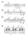
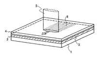
본 실시형태에서는, 비(非)단결정 반도체막을 결정화하는 방법, 및 결정화된 반도체막을 사용하여 반도체장치를 제작하는 방법을 설명한다. 도 1(A)∼도 1(C)는 비단결정 반도체막을 결정화하는 방법을 설명하기 위한 단면도이다.In this embodiment, a method of crystallizing a non-singlecrystalline semiconductor film and a method of manufacturing a semiconductor device using the crystallized semiconductor film are described. 1 (A) to 1 (C) are cross-sectional views for explaining a method for crystallizing a non-single crystal semiconductor film.
먼저, 도 1(A)에 나타내는 바와 같이, 기판(100)을 준비한다. 기판(100)으로서, 예를 들면, 유리 기판, 석영 기판, 사파이어 기판, 및 수지 기판 등의 절연 재료로 이루어지는 기판, 스테인리스 기판 등의 도전성 기판, 및 반도체 기판 등을 사용할 수 있다. 또한, 반도체장치의 제작공정의 가열 온도에 견딜 수 있는 경우에는, PET(폴리에틸렌 테레프탈레이트), PEN(폴리에틸렌 나프탈레이트), PES(폴리에테르 술폰), 폴리프로필렌으로 대표되는 플라스틱으로 이루어지는 기판이나, 아크릴 수지 등으로 대표되는 합성수지로 이루어지는 기판을 사용할 수 있다.First, as shown in Fig. 1 (A), a
스테인리스 기판 등의 도전성 기판 또는 반도체 기판을 사용하는 경우에는, 그 기판 표면에, 하지막으로서 기능하는 절연막을 형성하고, 이 절연막 위에 반도체막을 형성하여도 좋다. 또한, 유리 기판이나 수지 기판 등, 반도체막을 오염시키는 물질을 함유하는 기판을 사용하는 경우에도, 하지막으로서 기능하는 절연막으로 표면을 덮어, 반도체막이 오염되지 않게 하는 것이 바람직하다. 또한, 절연막을 두껍게 형성함으로써, 기판에 열이 전달되기 어렵게 하는 효과가 있고, 유리 기 판이나 플라스틱 기판과 같은 내열성이 낮은 기판의 사용을 가능하게 한다. 기판의 표면에 형성되는 절연막에는, 산화규소(SiOx), 질화규소(SiNx), 산화질화규소(SiOxNy, x > y > 0), 질화산화규소(SiOxNy, 0 < x < y) 등의 단층막 또는 적층막을 사용할 수 있다. 이들 절연막은 CVD법이나 스퍼터링법을 사용하여 형성할 수 있다.When a conductive substrate such as a stainless steel substrate or a semiconductor substrate is used, an insulating film serving as a base film may be formed on the substrate surface, and a semiconductor film may be formed on the insulating film. Further, even in the case of using a substrate containing a substance contaminating a semiconductor film such as a glass substrate or a resin substrate, it is preferable to cover the surface with an insulating film functioning as a base film to prevent the semiconductor film from being contaminated. Further, by forming the insulating film thick, it is possible to make it difficult to transfer heat to the substrate, and it is possible to use a substrate having low heat resistance such as a glass substrate or a plastic substrate. In the insulating film formed on a surface of a substrate, a silicon oxide (SiOx), silicon nitride (SiNx), silicon oxynitride(SiO x N y, x> y> 0), silicon oxynitride(SiO x N y, 0 < x < y) or the like can be used. These insulating films can be formed by a CVD method or a sputtering method.
본 실시형태에서는, 기판(100)에 유리 기판을 사용하고, 기판(100)의 표면에 하지막이 되는 절연막(101)을 막 두께 50 nm∼300 nm로 형성한다. 예를 들면, 절연막(101)으로서 막 두께 50 nm∼150 nm의 질화산화규소막과, 막 두께 50 nm∼150 nm의 산화질화규소막의 적층막을 CVD법으로 형성한다. 이 경우, 하층의 질화산화규소막은 상층의 산화질화규소막보다도 질소의 함유량이 많게 되도록 형성하는 것이 바람직하다. 하층의 질화산화규소막은, 질소의 함유량을 많게 함으로써, 오염 방지의 효과(패시베이션 효과)가 높아지도록 하고, 상층의 산화질화규소막은, 질소의 함유량을 억제하여, 결정성 반도체막과의 계면 준위 밀도가 높게 되지 않도록 한다. 또한, 하층의 질화산화규소막 대신에 질화규소막을 형성할 수도 있다. 또한, 상층의 산화질화규소막 대신에 산화규소막을 형성할 수도 있다.In this embodiment mode, a glass substrate is used for the
다음에, 결정화의 대상이 되는 반도체막(102)을 절연막(101) 위에 형성한다. 반도체막(102)은, 규소 또는 게르마늄을 주성분으로 하는 반도체로 형성할 수 있다. 예를 들면, 규소, 게르마늄, 규소게르마늄(Si1-xGex, 0 < x <1), 및 탄화규소(SiC) 등의 반도체이다. 이들 반도체로 이루어지는 막은 CVD법 또는 스퍼터링법 으로 형성할 수 있다. 또한, 반도체막(102)은, P(인), As(비소)와 같은 n형 불순물, 또는 B(붕소)와 같은 p형 불순물을 포함하여도 좋다.Next, a
레이저 빔을 조사하기 전의 반도체막(102)의 결정 구조는 비단결정이면 좋다. 예를 들면, 비정질, 미결정, 또는 다결정 구조이다.The crystal structure of the
반도체막(102)의 막 두께는 5 nm 이상 200 nm 이하로 할 수 있다. 반도체막(102)의 막 두께는, 바람직하게는 10 nm 이상 100 nm 이하, 보다 바람직하게는 10 nm 이상 80 nm 이하로 한다.The film thickness of the
또한, 하지막으로서 기능하는 절연막(101)은 필요에 따라 형성하면 좋고, 기판(100)이 유리인 경우에는, 유리로부터의 불순물이 반도체막(102)으로 확산하는 것을 방지하는 것이지만, 기판(100)으로서 석영 기판을 사용한 경우에는, 하지막으로서 기능하는 절연막(101)을 형성할 필요는 없다. 또한, 절연막(101)과 기판(100) 사이에 박리층을 형성하고, 기판(100) 위에 반도체 소자 등을 형성한 후에, 박리층에 박리를 발생시켜, 기판(100)으로부터 반도체 소자를 분리할 수도 있다.The insulating
다음에, 반도체막(102) 위에 캡(cap)막(103)을 형성한다. 캡막(103)에는, 레이저 빔의 파장에 대하여 충분한 투과율을 가지고, 열팽창 계수나 탄성률 등의 물성 값이 반도체막(102)의 것에 가까운 막을 사용하는 것이 바람직하다. 예를 들면, 캡막(103)은, 산화규소(SiOx), 질화규소(SiNx), 산화질화규소(SiOxNy, x > y > 0), 질화산화규소(SiOxNy, 0 < x < y)로부터 선택된 절연막의 단층막 또는 적층막으 로 형성할 수 있다. 캡막(103)을 적층막으로 한 경우, 박막에 의한 광 간섭 효과를 이용하여 반도체막(102)의 광 흡수 효율을 높일 수 있다. 이러한 적층 구조의 캡막(103)을 사용함으로써, 레이저 빔을 효율 좋게 흡수시킬 수 있기 때문에, 레이저의 사용 가능한 출력 범위를 넓힐 수 있다.Next, a
캡막(103)에는, 완전 용융한 반도체막(102)의 점성이 저하하는 것을 억제하는 효과, 축열 효과 등에 의하여, 완전 용융한 반도체막(102)에 난류가 발생하는 것을 억제하는 효과가 있다고 간주된다. 난류 억제 효과를 얻기 위하여, 캡막(103)의 막 두께는 100 nm 이상 1000 nm 이하, 보다 바람직하게는 200 nm 이상 600 nm 이하로 한다.It is considered that the
캡막(103)에, 상기 산화규소 등의 절연막을 사용하는 경우에는, 게이트 절연막과 동등한 강하고 치밀한 막인 것이 바람직하다. 이러한 강하고 치밀한 절연막은, 예를 들면, 성막 속도를 느리게 함으로써 형성할 수 있다. 성막 속도는 1 nm/min 이상 400 nm/min 이하, 바람직하게는 1 nm/min 이상 100 nm/min 이하로 한다.When an insulating film such as silicon oxide is used for the
다음에, 도 1(B)에 나타내는 바와 같이, 캡막(103)을 통하여, 선형 레이저 빔(105)을 주사하면서 선형 레이저 빔(105)을 반도체막(102)에 조사한다. 또한, 화살표 120은 선형 레이저 빔(105)의 주사 방향을 나타낸다. 반도체막(102)에서 선형 레이저 빔(105)이 조사되는 부분은 완전히 용융되고, 액체 상태의 반도체(106)가 된다. 선형 레이저 빔(105)이 기판에 대하여 상대적으로 이동함으로써, 반도체막(102)의 그 때까지 용융 상태이었던 부분이 냉각되고, 고화된 결과, 도 1(C)에 나타내는 바와 같이 결정성 반도체(107)가 형성된다.Next, as shown in Fig. 1B, the
도 2는 도 1(B)의 단면도에 대응하는 사시도이다. 선형 레이저 빔(105)을 주사함으로써, 반도체막(102) 내에서 고액 계면이 주사 방향으로 이동하기 때문에, 선형 레이저 빔(105)의 주사 방향으로 결정이 횡 성장하여, 도 2에 나타내는 바와 같이 주사 방향으로 긴 복수의 대입경 결정으로 이루어지는 결정성 반도체(107)가 형성된다. 그 결과, 결정성 반도체(107)에는, 주사 방향을 따라 복수의 입계가 형성된다. 결정립의 폭(입계의 간격)은, 액체 상태의 반도체(106)가 냉각되고 고화되는 시간에 의해 결정되고, 0.01 ㎛ 이상 10 ㎛ 이하가 된다.Fig. 2 is a perspective view corresponding to the sectional view of Fig. 1 (B). Fig. Since the solid-liquid interface moves in the scanning direction in the
본 발명은, 선형 레이저 빔(105)의 폭 W0를 가늘게 함으로써, 액체 형태의 반도체(106)에 온도 구배가 발생하는 것을 억제하고, 액체 상태의 반도체(106)에 난류가 발생하는 것을 억제하는 결정화 방법이다. 액체 상태의 반도체(106)에 난류를 발생하지 않게 함으로써, 서로 인접하는 결정립의 성장 방향, 성장 거리 등이 균일화되고, 그 결과, 결정성 반도체(107)의 각 결정립의 결정의 면 방위를 일치시킬 수 있다.The present invention can suppress the temperature gradient in the
따라서, 본 발명에서, 선형 레이저 빔(105)에 의하여 완전 용융된 반도체에 난류가 발생하지 않게 하기 위하여, 피조사면에서 선형 레이저 빔(105)의 폭 W0는, 결정성 반도체(107)의 결정립의 폭(입계의 간격)과 같은 정도로 하는 것이 바람직하다. 도 1에 나타내는 결정화 방법에서는, 캡막(103)에 난류 억제 효과가 있으므로, 선형 레이저 빔(105)의 폭 W0는 5 ㎛를 넘지 않도록 하면 좋고, 선형 레이저 빔(105)의 폭 W0의 바람직한 범위는 0.2 ㎛ 이상 5 ㎛ 이하이고, 보다 바람직한 범위는 0.2 ㎛ 이상 2 ㎛ 미만이다.Therefore, in the present invention, in order to prevent turbulence from being generated in the semiconductor completely melted by the
본 발명에서는, 캡막(103)을 형성하지 않고, 선형 레이저 빔(105)을 조사함으로써, 반도체막(102)을 측면 성장시킬 수도 있다. 이 경우는, 완전 용융한 반도체막(102)에 난류가 발생하는 것을 억제하기 위하여, 선형 레이저 빔(105)의 폭 W0는 2 ㎛를 넘지 않는 것이 바람직하고, 그 폭 W0는 0.2 ㎛ 이상 2 ㎛ 미만으로 하는 것이 바람직하다. 선형 레이저 빔(105)의 폭 W0를 2 ㎛ 미만의 매우 가는 폭으로 함으로써, 반도체막을 완전 용융시킬 수 있는 레이저 출력의 범위가 확장되고, 측면 성장한 결정성 반도체의 수율을 향상시킬 수 있다. 또한, 완전 용융한 반도체에 난류가 발생하는 것이 억제되기 때문에, 결정화된 반도체의 결정의 면 방위를 일치시킬 수 있다.In the present invention, the
다음에, 도 3을 사용하여, 폭 5 ㎛ 이하의 선형 레이저 빔을 조사하기 위한 레이저 조사 장치의 구성을 설명한다. 도 3은 본 발명의 레이저 조사 장치의 구성예를 나타낸다. 도 3에서, x 방향이 선형 레이저 빔의 장축 방향이고, 반도체막을 결정화하기 위해서는 y 방향으로 선형 레이저 빔을 주사한다.Next, the configuration of a laser irradiation apparatus for irradiating a linear laser beam with a width of 5 mu m or less will be described with reference to Fig. Fig. 3 shows a structural example of the laser irradiation apparatus of the present invention. In Fig. 3, the x direction is the long axis direction of the linear laser beam, and in order to crystallize the semiconductor film, a linear laser beam is scanned in the y direction.
도 3에 나타내는 바와 같이, 레이저 조사 장치는, 레이저 빔을 발진하는 레이저(151), 기판 고정용 스테이지(152), X 스테이지(153), Y 스테이지(154)를 가진다. 레이저(151)에는, 싱글 모드(보다 구체적으로는 횡 싱글 모드 TEM00) 또는 그 것에 가까운 레이저가, 멀티 모드보다도 반도체의 결정화에 적합하다. 싱글 모드의 레이저 빔의 프로파일이 가우스 분포이고, 멀티 모드의 레이저보다도 빔 프로 파일을 제어하기 쉽기 때문이다.3, the laser irradiation apparatus has a
레이저(151)에는, CW 레이저, 의사 CW 레이저 또는 펄스 발진 레이저 중 어느 종류의 레이저라도 사용할 수 있다. 레이저(151)에는, 예를 들면, KrF 레이저 등의 엑시머 레이저, Ar 레이저, Kr 레이저 등의 기체 레이저가 있다. 그 이외에, 고체 레이저로서, YAG 레이저, YVO4 레이저, YLF 레이저, YAlO3 레이저, GdVO4 레이저, KGW 레이저, KYW 레이저, 알렉산드라이트 레이저, Ti:사파이어 레이저, Y2O3 레이저 등이 있다.As the
레이저(151)의 레이저 매질로부터 발진되는 빔의 고조파를 사용하는 경우에는, 레이저(151)의 기본파를 고조파로 변환하는 비선형 광학 소자를 사용한다. 이 비선형 광학 소자는 레이저(151)에 내장되어 있어도 좋고, 레이저(151)에서 독립한 부품으로서 레이저 조사 장치에 설치되어도 좋다.When a harmonic of a beam emitted from the laser medium of the
기판 고정용 스테이지(152)는, 선형 레이저 빔이 조사되는 피처리물(Ob)을 흡착하여 고정하기 위한 장치이다. 기판 고정용 스테이지(152)는 X 스테이지(153)에 의하여 x 방향으로 이동되고, Y 스테이지(154)에 의하여 y 방향으로 이동된다. X 스테이지(153) 및 Y 스테이지(154)에 의하여 피조사물(Ob)을 이동시킴으로써, 피처리물(Ob)의 피조사면에서의 선형 레이저 빔 스폿(150)을 xy 평면에서 주사한다.The
또한, 도 3의 레이저 조사 장치는, 빔 스폿(150)을 고정시키고, X 스테이 지(153) 및 Y 스테이지(154)에 의하여 피처리물(Ob)을 이동시킴으로써, 선형 레이저 빔을 주사하는 구조이지만, 선형 레이저 빔의 주사는, 피처리물(Ob)을 고정시키고, 빔 스폿(150)을 이동시키는 구조라도 좋고, 양쪽 구조를 조합하여도 좋다.The laser irradiation apparatus shown in Fig. 3 has a structure for scanning a linear laser beam by fixing the
도 3의 레이저 조사 장치의 광학계는, 레이저(151)의 사출측으로부터, 슬릿(155), 편향 미러(156), 투영 렌즈(157), 집광 렌즈(158)가 순차로 배치되어 구성된다.3 includes a
편향 미러(156)는 광로를 편향시킬 필요가 있는 개소에 적절히 배치된다. 따라서, 편향 미러(156)의 위치 및 개수는 도 3에 한정되지 않고, 또한 편향 미러(156)를 설치하지 않아도 좋다.The
슬릿(155)은 레이저 빔의 프로파일을 균일화하기 위한 광학부재이다. 슬릿(155)은 빔 스폿(150)의 선형 레이저 빔의 x 방향의 양 끝을 차폐하도록 배치된다. 싱글 모드의 레이저 빔의 프로파일은 가우스 분포이고, 빔의 단부는, 반도체를 완전 용융시키기에는 강도가 부족하다. 슬릿(155)을 통과시킴으로써, 레이저 빔의 강도가 약한 부분이 피처리물(Ob)에 조사되지 않도록 한다. 또한, 레이저 빔의 조사 영역의 끝에 소입경 결정 또는 미(微)결정이 형성되는 것이 허용되는 경우에는, 슬릿(155)을 설치하지 않아도 좋다.The
투영 렌즈(157)는 슬릿(155)의 상(像)을 피조사물(Ob)에 투영하기 위한 렌즈이다. 그래서, 슬릿(155)이 피조사면과 공역 관계가 되도록, 투영 렌즈(157)가 배치된다. 도 3의 레이저 조사 장치에는, 투영 렌즈(157)에 볼록형 실린드리컬 렌즈를 사용하고, 빔 스폿(150)을 x 방향으로 집광하도록 이 실린드리컬 렌즈가 배치된 다. 볼록형 실린드리컬 렌즈 대신에, 볼록형 구면 렌즈라도 좋다. 또한, 투영 렌즈(157)를 집광 렌즈(158)의 사출측에 배치할 수도 있고, 투영 렌즈(157)를 생략하여도 좋다.The
집광 렌즈(158)는, 빔 스폿(150)을 폭 방향으로 집광하고, 폭 5 ㎛ 이하의 선 형상으로 가공하기 위한 렌즈이다. 도 3의 레이저 조사 장치에는, 집광 렌즈(158)에 볼록형 비구면 실린드리컬 렌즈가 사용되고, 빔 스폿(150)을 y 방향으로 집광하도록 이 비구면 실린드리컬 렌즈를 배치한다. 비구면 실린드리컬 렌즈를 사용함으로써, 종래의 실린드리컬 렌즈로는 어려웠던, 폭 5 ㎛ 이하의 선형 레이저 빔을 형성할 수 있고, 또한, 2 ㎛ 미만의 매우 가는 레이저 빔을 형성할 수도 있다. 비구면 실린드리컬 렌즈로 매우 가는 선형 레이저 빔을 형성할 수 있다는 점에 대하여는 후술한다.The
상기한 바와 같이, 집광 렌즈(158) 이외의 광학 부재는 필요에 따라 설치할 수 있는 부재이고, 도 3의 레이저 조사 장치는 집광 렌즈(158)를 가지면 좋고, 매우 단순한 구조의 광학계로 할 수 있다.As described above, the optical member other than the
또한, 도 3의 광학계에서, 피처리물(Ob)의 표면의 요철의 고저차(高低差)(표면 거치름)보다도, 집광 렌즈(158)의 초점 심도(深度)가 얕은 경우에는, 레이저 조사 장치에 오트포커스(autofocus) 장치를 설치하고, 선형 레이저 빔을 주사하면서 집광 렌즈(158)의 초점 위치를 조절할 수 있도록 한다. 집광 렌즈(158)의 초점 위치의 조절은 집광 렌즈(158)의 위치를 이동시켜 행한다(도 3의 경우에는, 집광 렌즈(158)를 z 방향으로 이동시킨다), 또는, 기판 고정용 스테이지(152)를 상하(z축 방향)으로 이동시킴으로써 행할 수 있다. 집광 렌즈(158)를 이동시키는 타입의 장치가, 이동되는 대상이 가볍기 때문에, 오트포커스 장치로서 바람직하다.3, when the depth of focus of the
도 3의 레이저 조사 장치를 사용하여 반도체막을 결정화하기 위해서는, 도 1(A)에 나타내는, 절연막(101), 반도체막(102) 및 캡막(103)을 형성한 기판(100)을 피처리물(Ob)로 하여 기판 고정용 스테이지(152)에 고정한다. 기판(100)을 이동시킴으로써, 선형 레이저 빔을 주사하면서, 그 레이저 빔을 반도체막(102)에 조사할 수 있다. 주사 속도는, 사용하는 레이저(151)의 발진 방식, 레이저(151)의 출력, 반도체막(102)의 재료 및 막 두께, 캡막(103)의 유무(有無), 및 구조와 막 두께 등을 고려하여 결정할 수 있다. 특히, 레이저(151)에 펄스 발진 레이저를 사용하는 경우에는, 선형 레이저 빔의 조사 영역을 주사 방향으로 겹쳐, 반도체막(102)이 측면 성장하도록 주사 속도를 제어한다.In order to crystallize the semiconductor film using the laser irradiation apparatus of Fig. 3, the
기판(100)의 한 변으로부터 그의 대변(對邊)까지 y 방향으로 소정의 거리에서 선형 레이저 빔을 주사한 후, 선형 레이저 빔의 길이 또는 그 길이 이상, X 스테이지(153)에 의하여 기판(100)을 x 방향으로 이동시켜, 반도체막(102)의 결정화되지 않는 부분에 빔 스폿(150)이 조사되도록 위치맞춤을 행한다. 다시, Y 스테이지(154)에 의하여 기판(100)을 y 방향으로 이동시키면서, 선형 레이저 빔을 조사한다. 이상의 일련의 동작을 반복함으로써, 반도체막(102)의 소망의 부분을 결정화하여 결정성 반도체(107)를 형성할 수 있다.A linear laser beam is scanned at a predetermined distance in the y direction from one side of the
다음에, 도 4를 사용하여, 본 발명의 결정화 방법으로 형성된 결정성 반도체(107)로부터 반도체장치를 제작하는 방법을 설명한다.Next, a method of manufacturing a semiconductor device from the
결정화 공정을 완료함으로써, 도 1(C)에 나타내는 바와 같이, 기판(100) 위에 결정성 반도체(107)가 형성된다. 다음에, 반도체장치를 제조하기 위하여, 도 4(A)에 나타내는 바와 같이, 에칭 처리에 의하여 캡막(103)을 제거한다.By completing the crystallization process, the
다음에, 결정성 반도체(107) 위에 레지스트를 도포한다. 레지스트를 노광하고 현상함으로써 소망의 형상으로 레지스트를 형성한다. 이 레지스트를 마스크로 하여 에칭을 행하여, 결정성 반도체(107)를 부분적으로 제거한다. 이 공정에 의하여, 도 4(B)에 나타내는 바와 같이, 절연막(101) 위에 섬 형상의 결정성 반도체막(108)을 형성한다. 형성된 결정의 면 방위가 일치된 결정성 반도체(107)를 보호하기 위하여, 레지스트의 형성을 행하기 전에, 결정성 반도체(107)의 표면을 산화하면 좋다. 이 산화막은 레지스트의 습윤성을 향상시키는 효과도 있다. 여기서의 산화 처리에는, 예를 들면, 오존 함유 수용액의 도포, 또는 산소 분위기에서 UV 조사함으로써 얻어진 오존에 의한 처리가 사용된다.Next, a resist is applied on the
섬 형상의 결정성 반도체막(108)을 사용하여 박막트랜지스터, 다이오드, 저항 소자, 콘덴서, 광전 변환 소자, 전하 결합 소자 등의 반도체장치를 구성하는 반도체 소자를 형성한다. 여기서는, 반도체장치 제작방법의 일 형태로서 박막트랜지스터(이하, TFT라고 약기(略記)한다)를 제작한다.A semiconductor element constituting a semiconductor device such as a thin film transistor, a diode, a resistance element, a capacitor, a photoelectric conversion element, or a charge coupled device is formed by using the island-shaped
또한, TFT를 제작하는 경우, 섬 형상의 결정성 반도체막(108)을 형성하기 위한 레지스터를 형성하기 전에, TFT의 스레시홀드 전압을 제어하기 위하여 미량의 불순물 원소(붕소 또는 인)를 결정성 반도체(107)에 도핑한다. 또한, 이 도핑은 필요에 따라 행하면 좋다.Further, in the case of manufacturing the TFT, before forming the resistor for forming the island-shaped
도 4(C)에 나타내는 바와 같이, 결정성 반도체막(108) 위에 절연막(109)을 형성한다. 절연막(109)은 TFT의 게이트 절연막으로서 기능한다. 예를 들면, 절연막(109)으로서 산화규소막을 형성한다.The insulating
다음에, 절연막(109) 위에 도전막을 형성한다. 이 도전막에는, 힐록(hillock)의 발생이 적은, W, Mo, Ti, Ta, Co 등으로부터 선택되는 고융점 금속, 및 질화텅스텐, 질화몰리브덴, 질화티탄, 질화탄탈 등의 고융점 금속의 화합물을 사용하는 것이 바람직하다. 도전막은 단층이라도 좋고, 적층이라도 좋다. 에칭 처리에 의하여 도전막을 소망의 형상으로 가공하여 게이트 배선(110)을 형성한다.Next, a conductive film is formed on the insulating
다음에, 게이트 배선(110)을 형성할 때 사용한 레지스트를 마스크로 사용하여, 결정성 반도체막(108)에 도전형을 부여하는 불순물 원소(P, As 등)를 도핑한다. 여기서는, n채널형 TFT를 제작하기 위하여, 인, 비소와 같은, n형을 부여하는 불순물 원소를 첨가하여, n형 불순물 영역(112)을 형성한다. n형 불순물 영역(112)은 소스 영역 또는 드레인 영역으로서 기능한다. 또한, p채널형 TFT를 제작하는 경우에는, 붕소와 같은, p형을 부여하는 불순물 원소를 도입한다.Next, the
도전형을 부여하는 불순물 원소를 결정성 반도체막(108)에 첨가함으로써, 결정성 반도체막(108)의 게이트 배선(110)과 겹치는 영역에 채널 형성 영역(113)이 형성된다.The
불순물 원소를 첨가한 후, 불순물 원소를 활성화하기 위하여 가열 처리 또는 레이저 빔 조사를 행한다. 이 처리에 의하여, 불순물 원소의 활성화와 동시에 절연막(109)에의 플라즈마 손상(damage)이나, 절연막(109)과 결정성 반도체막(108)과 의 계면에 발생한 플라즈마 손상을 회복시킬 수 있다.After adding the impurity element, heat treatment or laser beam irradiation is performed to activate the impurity element. By this treatment, plasma damage to the insulating
다음에, 도 4(D)에 나타내는 바와 같이, 절연막(114)을 형성한다. 그리고, 절연막(114) 및 절연막(109)을 에칭하여, n형 불순물 영역(112)에 도달하는 콘택트 홀을 형성한다. 절연막(114) 위에 도전막을 형성한다. 도전막을 에칭에 의하여 소망의 형상으로 가공하여 배선(115)을 형성한다. 여기서는, 배선(115)은 소스 배선 또는 드레인 배선으로서 기능한다.Next, as shown in Fig. 4 (D), an insulating
배선(115)을 구성하는 도전막은, 예를 들면, W, Mo, Ti, Al, Cu로부터 선택된 금속, 또는 이들 금속을 주성분으로 하는 합금, 및 이들 금속을 주성분으로 하는 화합물에서 선택되는 재료로 형성할 수 있다. 또한, 도전막은 단층이라도 좋고, 다층이라도 좋다. 도전막을 다층막으로 하기 위해서는, 예를 들면, Ti 막, Al 막, Ti 막의 순서로 적층하여 형성한다.The conductive film constituting the
이상의 공정에 의하여, 도 4(D)에 나타내는 바와 같이 기판(100) 위에 TFT가 형성된다. 결정성 반도체막(108)은, 결정의 면 방위가 일치된 결정성 반도체막이기 때문에, 기판(100) 위의 복수의 TFT의 전기적 특성의 편차를 억제할 수 있다. 또한, 서브스레시홀드 값이 적고, 온(ON) 전류가 크고, 전계효과 이동도가 높다는 뛰어난 전기적 특성의 TFT를 제작할 수 있다. 따라서, 이러한 TFT에 의하여, 저소비전력으로 고속으로 동작하는 집적회로를 제작할 수 있다.Through the above steps, a TFT is formed on the
본 발명의 결정화 방법을 사용하여 형성된 결정성 반도체막을 사용하여 각종의 반도체장치를 제작할 수 있다. 이하의 실시형태에서, 각종의 반도체장치의 제작방법을 설명한다.Various semiconductor devices can be manufactured using the crystalline semiconductor film formed using the crystallization method of the present invention. In the following embodiments, various semiconductor device manufacturing methods will be described.
[실시형태 2][Embodiment 2]
본 실시형태에서는, 반도체장치의 일례인 액정 표시장치의 제작방법에 대하여 도 5 및 도 6을 사용하여 설명한다.In this embodiment, a method of manufacturing a liquid crystal display device, which is an example of a semiconductor device, will be described with reference to Figs. 5 and 6. Fig.
도 5(A)에 나타내는 바와 같이, 실시형태 1과 마찬가지로, 기판(100) 위에 하지막으로서 기능하는 절연막(101)을 형성하고, 이 절연막(101) 위에 비단결정 구조의 반도체막(102)을 형성하고, 이 반도체막(102) 위에 캡막(103)을 형성한다.An insulating
여기서는, 기판(100)으로서 유리 기판을 사용한다. 절연막(101)으로서는, 막 두께 40 nm∼60 nm의 질화산화규소막(SiOxNy, 0 < x < y)을 플라즈마 CVD법에 의하여 형성한다. 또한, 반도체막(102)으로서 플라즈마 CVD법에 의하여, 가스에 SiH4 및 H2를 사용하여, 막 두께 10 nm∼80 nm의 비정질 규소막을 형성한다. 캡막(103)으로서는, 플라즈마 CVD법에 의하여 막 두께 200 nm∼1000 nm의 질화산화규소막(SiOxNy, 0 < x < y)을 형성한다. 예를 들면, 가스에 SiH4(유량 10 sccm), NH3(유량 100 sccm), N2O(유량 20 sccm), H2(유량 400 sccm)를 사용함으로써, 산소를 10 원자% 이하 함유하고, 규소에 대한 질소의 조성비가 1.3 이상 1.5 이하인 질소산화규소막이 형성된다.Here, a glass substrate is used as the
다음에, 선형 레이저 빔(105)을 주사하면서, 도 5(B)에 나타내는 바와 같이, 캡막(103)을 통하여 반도체막(102)에 선형 레이저 빔(105)을 조사한다. 선형 레이저 빔(105)을 조사함으로써, 반도체막(102)이 완전 용융하여, 액체 상태의 반도 체(106)가 된다. 선형 레이저 빔(105)을 주사함으로써, 완전 용융한 반도체막(102)이 측면 성장하여, 절연막(101) 위에 대입경 결정으로 이루어지는 결정성 반도체(107)가 형성된다. 본 발명에서는, 선형 레이저 빔(105)의 폭을 5 ㎛ 이하로 함으로써, 완전 용융된 반도체막(102)에 난류가 발생하는 것이 억제되기 때문에, 결정성 반도체(107)를 결정의 면 방위가 일치된 결정성 반도체로 할 수 있다.Next, while scanning the
또한, 반도체막(102)이나 캡막(103)에 수소가 함유되어 있는 경우, 선형 레이저 빔의 조사에 의하여 수소의 분출을 방지하기 위하여, 선형 레이저 빔(105)의 조사 전에 가열 처리를 행하여, 수소 농도를 낮춘다.In the case where hydrogen is contained in the
결정성 반도체(107)를 형성한 후, 캡막(103)을 제거한다. 캡막(103)의 제거 방법으로서는, 건식 에칭, 습식 에칭, 연마 등의 각종 제거 방법을 사용할 수 있다. 여기서는 건식 에칭법에 의하여 캡막(103)을 제거한다.After the
다음에, 도 5(C)에 나타내는 바와 같이, 결정성 반도체(107)를 선택적으로 에칭하여 반도체층(201∼203)을 형성한다. 결정성 반도체(107)의 에칭 방법으로서는, 건식 에칭, 습식 에칭 등을 사용할 수 있지만, 여기서는 결정성 반도체(107) 위에 레지스트를 도포한 후, 노광 및 현상을 행하여 레지스트 마스크를 형성한다. 그 형성된 레지스트 마스크를 사용하여, SF6: O2의 유량비를 4 : 15로 한 건식 에칭법에 의하여 결정성 반도체(107)(결정성 규소)를 선택적으로 에칭하고, 그 후, 레지스트 마스크를 제거한다.Next, as shown in Fig. 5C, the
다음에, 도 5(D)에 나타내는 바와 같이, 반도체층(201∼203) 위에 절연 막(204)을 형성한다. 이 절연막(204)은 박막트랜지스터의 게이트 절연막으로서 기능한다. 이 절연막(204)은 산화규소(SiOx), 질화규소(SiNx), 산화질화규소(SiOxNy, x > y > 0), 질화산화규소(SiOxNy, 0 < x < y) 등의 단층막 또는 적층막으로 형성한다. 여기서는, 절연막(204)으로서 막 두께 115 nm의 산화질화규소를 플라즈마 CVD법에 의하여 형성한다.Next, as shown in Fig. 5 (D), an insulating
다음에, 절연막(204)을 사이에 두고 반도체층(201∼203) 위에 게이트 전극(205∼208)을 형성한다. 게이트 전극(205∼208)은, 금속, 합금, 금속 화합물 또는 일 도전형의 불순물을 첨가한 다결정 반도체로 형성할 수 있다.Next,
금속을 사용하는 경우에는, 텅스텐(W), 몰리브덴(Mo), 티탄(Ti), 탄탈(Ta), 알루미늄(Al) 등을 사용할 수 있다. 또한, 금속을 질화시킨 금속 질화물을 사용할 수도 있고, 그 외에, 상기 금속 질화물로 이루어지는 제1 층과 상기 금속으로 이루어지는 제2 층을 적층시킨 구조로 하여도 좋다. 이들 재료는 스퍼터링법, 증착법 등으로 형성할 수 있다.In the case of using a metal, tungsten (W), molybdenum (Mo), titanium (Ti), tantalum (Ta), aluminum (Al) and the like can be used. Alternatively, a metal nitride obtained by nitriding a metal may be used, or a first layer made of the metal nitride and a second layer made of the metal may be laminated. These materials can be formed by a sputtering method, a vapor deposition method, or the like.
또한, 액적 토출법을 사용하여, 미립자를 함유하는 페이스트를 게이트 절연막 위에 토출하고, 건조·소성을 함으로써, 게이트 전극(205∼208)을 형성할 수 있다. 또한, 절연막(204) 위에, 미립자를 함유하는 페이스트를 인쇄하고 건조시킨 후, 페이스트를 소성함으로써, 게이트 전극(205∼208)을 형성할 수도 있다. 대표적인 미립자에는, 금, 구리, 금과 은의 합금, 금과 구리의 합금, 은과 구리의 합금, 금과 은과 구리의 합금 등이 있다.Further, the
여기서는, 절연막(204) 위에, 스퍼터링법에 의하여, 막 두께 30 nm의 질화탄탈막 및 막 두께 370 nm의 텅스텐막의 적층막을 형성한다. 그 후, 포토리소그래피 공정에 의하여 형성한 레지스트 마스크를 사용하여 상기 적층막을 에칭하여, 질화탄탈막의 단부가 텅스텐막의 단부보다 외측으로 돌출한 구조의 게이트 전극(205∼208)을 형성한다.Here, a lamination film of a tantalum nitride film with a thickness of 30 nm and a tungsten film with a thickness of 370 nm is formed on the insulating
다음에, 게이트 전극(205∼208)을 마스크로 하여 반도체층(201∼203)에 n형을 부여하는 불순물 원소 또는 p형을 부여하는 불순물 원소를 첨가하여, 고농도 불순물 영역(209∼215)을 형성한다. 또한, 게이트 전극(205∼208)의 일부와 겹치는 저농도 불순물 영역(216∼223)을 형성한다.Next, an impurity element imparting n-type or p-type impurity element is added to the semiconductor layers 201-203 using the gate electrodes 205-208 as a mask to form high concentration impurity regions 209-215 . In addition, low-
또한, 여기서는, 고농도 불순물 영역(209, 210, 213, 214, 215) 및 저농도 불순물 영역(216, 217, 220∼223)에, p형을 부여하는 불순물 원소인 붕소를 도핑한다. 또한, 고농도 불순물 영역(211, 212) 및 저농도 불순물 영역(218, 219)에, n형을 부여하는 불순물 원소인 인을 도핑한다. 반도체층(201∼203)에 불순물 원소를 도핑함으로써, 자기정합적으로 채널 형성 영역(201c∼203c)이 형성된다.Here, boron, which is an impurity element that imparts p-type conductivity, is doped into the high-
그 후, 반도체층(201∼203)에 첨가된 불순물 원소를 활성화하기 위하여 가열 처리를 행하는데, 여기서는 질소 분위기에서 550℃, 4시간의 가열을 행한다. 이상의 공정에 의하여, 박막트랜지스터(225∼227)이 형성된다.Thereafter, heat treatment is performed to activate the impurity element added to the semiconductor layers 201 to 203. Here, heating is performed at 550 DEG C for 4 hours in a nitrogen atmosphere. Through the above process, the
또한, 박막트랜지스터(225, 227)는 p채널형 박막트랜지스터이고, 박막트랜지스터(226)는 n채널형 박막트랜지스터이다. p채널형 박막트랜지스터(225) 및 n채널형 박막트랜지스터(226)에 의하여 구동회로를 구성하고, p채널형 박막트랜지스 터(227)는 화소의 전극에 전압을 인가하는 스위칭 소자로서 기능한다. 또한, 화소의 박막트랜지스터(227)는 n채널형 트랜지스터로 하여도 좋다. 여기서는, 구동회로에는, n채널형 및 p채널형 양쪽의 트랜지스터를 형성하였지만, n채널형만 또는 p채널형만을 형성할 수도 있다.The
다음에, 도 6(A)에 나타내는 바와 같이, 박막트랜지스터(225∼227) 위에 제1 층간절연막을 형성한다. 여기서는, 제1 층간절연막으로서, 산화규소막(231), 질화규소막(232) 및 산화규소막(233)을 적층하여 형성한다.Next, as shown in FIG. 6A, a first interlayer insulating film is formed on the
다음에, 제1 층간절연막의 일부인 산화규소막(233) 위에 박막트랜지스터(225∼227)의 고농도 불순물 영역에 접속되는 배선(234∼239), 및 접속 단자(240)를 형성한다. 여기서는, 스퍼터링법에 의하여, Ti막 100 nm, Al막 700 nm, Ti막 100 nm를 연속적으로 성막하여 적층막을 형성한다. 다음에, 포토리소그래피 공정에 의하여 형성한 레지스트 마스크를 사용하여, 상기 적층막을 에칭하여, 배선(234∼239) 및 접속 단자(240)를 형성한다.Next, wirings 234 to 233 connected to the high concentration impurity regions of the
다음에, 배선(234∼239) 및 접속 단자(240) 위에 제2 층간절연막(241)을 형성한다. 제2 층간절연막(241)은, 산화규소, 질화규소 또는 산화질화규소(질소를 함유하는 산화규소 또는 산소를 함유하는 질화규소) 등의 무기 절연 재료의 단층막 또는 적층막으로 형성하면 좋다. 이러한 무기 절연 재료로 이루어지는 막을 형성하는 방법으로서는, 스퍼터링법, LPCVD법, 또는 플라즈마 CVD법 등을 사용하면 좋다.Next, a second
여기서는, 플라즈마 CVD법을 사용하여 막 두께 100 nm∼150 nm의 산소를 함 유하는 질화규소막을 형성한 후, 포토리소그래피 공정에 의하여 형성한 레지스트 마스크를 사용하여, 산소를 함유하는 질화규소막을 선택적으로 에칭하여, 박막트랜지스터(227)의 배선(239) 및 접속 단자(240)에 달하는 콘택트 홀을 형성함과 함께, 제2 층간절연막(241)을 형성하고, 그 후, 레지스트 마스크를 제거한다. 본 실시형태와 같이, 제2 층간절연막(241)을 형성함으로써, 구동회로부의 TFT나 배선 등의 노출을 방지할 수 있어, 오염을 회피할 수 있다.Here, a silicon nitride film containing oxygen in a thickness of 100 nm to 150 nm is formed by a plasma CVD method, and then a silicon nitride film containing oxygen is selectively etched by using a resist mask formed by a photolithography process A contact hole reaching the
다음에, 박막트랜지스터(227)의 배선(239)에 접속하는 제1 화소 전극(242), 및 접속 단자(240)와 접속하는 도전층(244)을 형성한다. 액정 표시장치가 투광형 액정 표시장치인 경우에는, 제1 화소 전극(242)을 투광성을 가지는 도전막으로 형성한다. 또한, 액정 표시장치가 반사형 액정 표시장치인 경우에는, 제1 화소 전극(242)을 반사성을 가지는 도전막으로 형성한다. 또한, 반투광형으로 하는 경우에는, 제1 화소 전극(242)의 일부를 투광성을 가지는 도전막으로 형성하고, 나머지 부분을 반사성을 가지는 도전막으로 형성한다.Next, the
여기서는, 액정 표지장치를 투과형으로 한다. 스퍼터링법에 의하여 막 두께 125 nm의 산화규소를 함유하는 ITO를 성막한다. 포토리소그래피 공정에 의하여 형성한 레지스트 마스크를 사용하여 상기 ITO막을 에칭하여, 제1 화소 전극(242) 및 도전층(244)을 형성한다.Here, the liquid crystal labeling apparatus is of the transmission type. ITO containing silicon oxide with a film thickness of 125 nm is formed by a sputtering method. The ITO film is etched using a resist mask formed by a photolithography process to form a
다음에, 배향막으로서 기능하는 절연막(243)을 형성한다. 또한, 배향막은 필요에 따라 형성하면 좋다. 절연막(243)은 폴리이미드나 폴리비닐 알코올 등의 고분자 화합물층을 롤 코팅법, 인쇄법 등에 의하여 형성한 후, 러빙 처리함으로써 형성할 수 있다. 또한, 기판에 대하여 비스듬한 각도에서 SiO2를 증착함으로써 절연막(243)을 형성할 수 있다. 또한, 광 반응형 고분자 화합물에 편광된 UV광을 조사하여 광 반응형 고분자 화합물을 중합시킴으로써 절연막(243)을 형성할 수도 있다. 여기서는, 폴리이미드나 폴리비닐 알코올 등의 고분자 화합물층을 인쇄하고, 소성한 후, 러빙 처리함으로써 형성한다.Next, an insulating
다음에, 도 6(B)에 나타내는 바와 같이, 대향 기판(251)에 투광성을 가지는 도전막으로 이루어지는 제2 화소 전극(253)을 형성하고, 제2 화소 전극(253) 위에 배향막으로서 기능하는 절연막(254)을 형성한다. 대향 기판(251)으로서는, 기판(100)과 같은 재료를 적절히 선택할 수 있다. 또한, 제2 화소 전극(253)은 제1 화소 전극(242)과 같은 방식으로 형성할 수 있고, 배향막으로서 기능하는 절연막(254)은 절연막(243)과 같은 방식으로 형성할 수 있다. 또한, 대향 기판(251) 및 제2 화소 전극(253) 사이에, 컬러 필터로서 기능하는 착색층(252)은 필요에 따라 형성하면 좋다. RGB 방식의 컬러 표시를 행하는 경우에는, 착색층(252)으로서, 적색, 녹색, 청색의 각 색에 대응한 염료나 안료가 분산된 착색층을 각 화소에 대응하여 형성한다.Next, as shown in Fig. 6B, a
다음에, 기판(100)과 대향 기판(251)을 시일(seal)재(257)로 접합시키고, 기판(100)과 대향 기판(251) 사이에 액정층(255)을 형성한다. 그 액정층(255)은, 모세관 현상을 이용한 진공 주입법에 의하여, 배향막으로서 기능하는 절연막(243, 254) 및 시일재(257)로 둘러싸인 영역에 액정 재료를 주입함으로써 형성할 수 있 다. 또한, 대향 기판(251)의 한쪽 표면에 시일재(257)를 형성하고, 그 시일재(257)로 둘러싸인 영역에 액정 재료를 적하한 후, 감압 하에서 기판(100)과 대향 기판(251)을 압착시켜, 시일재(257)로 2장의 기판의 틈을 봉지(封止)함으로써, 액정층(255)을 형성할 수도 있다.Next, the
시일재(257)로서는, 열 경화형 에폭시 수지, UV 경화형 아크릴 수지, 열 가소형 나일론 수지 및 폴리에스테르 수지 등을 사용할 수 있다. 또한, 기판(100)과 대향 기판(251) 사이의 간격을 유지하기 위하여, 시일재(257)에 충전제(filler)를 함유시키는 것이 바람직하다.As the sealing
또한, 기판(100)과 대향 기판(251) 사이의 간격을 유지하기 위하여, 배향막으로서 기능하는 절연막(243, 254)들 사이에 스페이서(256)를 형성하여도 좋고, 그 스페이서(256)로서는, 유기 수지를 도포하고, 그 유기 수지를 소망의 형상, 대표적으로는 기둥 형상 또는 원주 형상으로 에칭하여 형성할 수 있다. 또한, 스페이서(256)로서, 비드(bead) 스페이서를 사용하여도 좋으므로, 여기서는 스페이서(256)로서 비드 스페이서를 사용한다. 또한, 도시하지 않았지만, 기판(100)과 대향 기판(251) 중의 어느 한쪽 또는 양쪽에 편광판을 설치한다.A
다음에, 도 6(C)에 나타내는 바와 같이, 단자부(263)에서는, 박막트랜지스터의 게이트 배선, 소스 배선에 접속되는 접속 단자(도 6(C)에서는, 소스 배선 또는 드레인 배선에 접속되는 접속 단자(240)를 나타낸다)가 형성된다. 그 접속 단자(240)에, 도전층(244) 및 이방성 도전막(261)을 통하여 FPC(flexible printed circuit)(262)가 접속되고, 접속 단자(240)에는 도전층(244) 및 이방성 도전 막(261)을 통하여 비디오 신호나 클록 신호가 입력된다.Next, as shown in Fig. 6 (C), in the
구동회로부(264)에는, 소스 드라이버나 게이트 드라이버 등의, 화소를 구동하는 회로가 형성되고, 여기서는 n채널형 박막트랜지스터(226) 및 p채널형 박막트랜지스터(225)에 의하여 CMOS 회로가 형성되어 있다.A circuit for driving pixels such as a source driver and a gate driver is formed in the
화소부(265)에는, 복수의 화소가 형성되고, 각 화소에는 액정소자(258)가 형성되고, 그 액정소자(258)는, 제1 화소 전극(242), 제2 화소 전극(253) 및 그 전극들 사이에 충전되는 액정층(255)이 겹치는 부분이다. 또한, 그 액정소자(258)가 가지는 제1 화소 전극(242)은 박막트랜지스터(227)와 전기적으로 접속되어 있다.A plurality of pixels are formed in the
이상의 공정에 의하여 액정 표시장치가 제작될 수 있고, 본 실시형태에서 나타내는 액정 표시장치는, 구동회로부(264)나 화소부(265)에 형성되는 박막트랜지스터의 반도체층에서, 결정의 면 방위가 일정 방향으로 일치하여 있다. 따라서, 복수의 박막트랜지스터의 전기 특성의 편차를 억제할 수 있고, 그 결과, 색 불균일이나 결함이 없는 액정 표시장치를 제작할 수 있다.The liquid crystal display device shown in this embodiment can be manufactured in the same manner as the liquid crystal display device of this embodiment except that the plane orientation of the crystal is constant in the semiconductor layer of the thin film transistor formed in the
또한, 상기와 같은 전기적 특성이 뛰어난 박막트랜지스터를 형성할 수 있기 때문에, 액티브 매트릭스형의 액정 표시장치의 저소비전력화, 고정세화를 실현할 수 있다.In addition, since a thin film transistor having excellent electrical characteristics as described above can be formed, low power consumption and high definition can be realized in an active matrix type liquid crystal display device.
[실시형태 3][Embodiment 3]
본 실시형태에서는, 반도체장치의 일례인 발광소자를 가지는 발광장치의 제작공정에 대하여 설명한다.In this embodiment, a manufacturing process of a light emitting device having a light emitting element which is an example of a semiconductor device will be described.
실시형태 1과 같은 공정에 의하여, 기판(100) 위에 절연막(101)을 사이에 두 고 결정성 반도체를 형성한다. 그리고, 도 7(A)에 나타내는 바와 같이, 실시형태 2와 같은 공정에 의하여, 이 결정성 반도체를 사용하여 박막트랜지스터(225∼227)를 형성한다.A crystalline semiconductor is formed by depositing the insulating
그 박막트랜지스터(225∼227)의 게이트 전극 위에, 제1 층간절연막으로서, 산화규소막(231), 질화규소막(232) 및 산화규소막(233)을 적층하여 형성한다. 또한, 제1 층간절연막의 일부인 산화규소막(233) 위에 박막트랜지스터(225∼227)의 반도체층에 접속하는 배선(308∼313), 및 접속 단자(314)를 형성한다.A
다음에, 제1 층간절연막, 배선(308∼313), 및 접속 단자(314) 위에 제2 층간절연막(315)을 형성한다. 그 후, 박막트랜지스터(227)의 배선(313)에 접속하는 제1 전극층(316), 및 접속 단자(314)와 접속하는 도전층(320)을 형성한다. 그 제1 전극층(316) 및 도전층(320)은, 스퍼터링법에 의하여 막 두께 125 nm의 산화규소를 포함하는 ITO를 성막한 후, 포토리소그래피 공정에 의하여 형성한 레지스트 마스크를 사용하여 ITO를 선택적으로 에칭하여 형성한다. 본 실시형태와 같이, 제2 층간절연막(315)을 형성함으로써, 구동회로부의 TFT나 배선 등의 노출을 방지하여, 오염 물질로부터 구동회로를 보호할 수 있다.Next, a second
다음에, 제1 전극층(316)의 단부를 덮는 유기 절연물막(317)을 형성한다. 여기서는, 감광성 폴리이미드를 도포하고 소성한 후, 노광 및 현상을 행하여, 구동회로부, 화소부의 제1 전극층(316), 및 화소부의 주변부의 제2 층간절연막(315)이 노출되도록 유기 절연물막(317)을 형성한다.Next, an organic
다음에, 제1 전극층(316) 및 유기 절연물막(317)의 일부 위에 증착법에 의하 여 발광물질을 함유하는 층(318)을 형성하는데, 그 발광물질을 함유하는 층(318)은 발광성을 가지는 유기 화합물, 또는 발광성을 가지는 무기 화합물로 형성한다. 또한, 발광물질을 함유하는 층(318)은 발광성을 가지는 유기 화합물 및 발광성을 가지는 무기 화합물로 형성하여도 좋다. 또한, 발광물질을 함유하는 층(318)을 적색 발광성의 발광물질, 청색 발광성의 발광물질, 및 녹색 발광성의 발광물질을 사용하여, 각각 적색 발광성의 화소, 청색 발광성의 화소, 및 녹색 발광성의 화소를 형성할 수 있다.Next, a
여기서는, 적색 발광성의 발광물질을 함유하는 층으로서, DNTPD를 50 nm, NPB를 10 nm, 비스[2,3-비스(4-플루오로페닐)퀴녹살리나토]이리듐(아세틸아세토네이트)(약칭 : Ir(Fdpq)2(acac))가 첨가된 NPB를 30 nm, Alq3를 60 nm, 및 LiF를 1 nm 적층하여 형성한다. 또한, 녹색 발광성의 발광물질을 함유하는 층으로서, DNTPD를 50 nm, NPB를 10 nm, 쿠마린 545T(C545T)가 첨가된 Alq3를 40 nm, Alq3를 60 nm, 및 LiF를 1 nm를 적층하여 형성한다.Here, as a layer containing a red light-emitting luminescent material, DNTPD of 50 nm, NPB of 10 nm, bis [2,3-bis (4-fluorophenyl) quinoxalinato] iridium (acetylacetonate) 30 nm of NPB doped with Ir (Fdpq)2 (acac)), 60 nm of Alq3 , and 1 nm of LiF. As the layer containing the luminescent material of green luminescence, 50 nm of DNTPD, 10 nm of NPB, 40 nm of Alq3 to which coumarin 545T (C545T) was added, 60 nm of Alq3 and 1 nm of LiF were laminated .
또한, 청색 발광성의 발광물질을 함유하는 층으로서, DNTPD를 50 nm, NPB를 10 nm, 2,5,8,11-테트라(tert-부틸)페릴렌(약칭 : TBP)이 첨가된 9-[4-(N-카르바졸일)]페닐-10-페닐안트라센(약칭 : CzPA)을 30 nm, Alq3를 60 nm, 및 LiF를 1 nm 적층하여 형성한다. 또한, 백색 발광성의 발광물질을 사용하여 발광물질을 함유하는 층을 형성함으로써, 적색 발광성의 화소, 청색 발광성의 화소, 및 녹색 발광성의 화소 외에, 백색 발광성의 화소를 형성하여도 좋다. 또한, 백색 발광성의 화소를 형성함으로써 소비전력을 삭감할 수 있다.As a layer containing a blue light emitting luminescent material, DNTPD was doped to 50 nm, NPB was doped to 10 nm, and 9- [(tert -butyl) perylene (TBP) (Abbreviation: CzPA) of 30 nm, Alq3 of 60 nm, and LiF of 1 nm are laminated on the substrate. Further, by forming a layer containing a luminescent material by using a luminescent material of white luminescence, a pixel of luminescent white color may be formed in addition to a pixel of red luminescent color, a pixel of blue luminescent color, and a pixel of green luminescent color. Further, by forming pixels of white luminescent property, power consumption can be reduced.
다음에, 발광물질을 함유하는 층(318) 및 유기 절연물 막(317) 위에 제2 전극층(319)을 형성하는데, 여기서는, 막 두께 200 nm의 Al막을 증착법에 의하여 형성한다. 그 결과, 제1 전극층(316), 발광물질을 함유하는 층(318), 및 제2 전극층(319)에 의하여 발광소자(321)가 구성된다.Next, a
발광물질을 함유하는 층(318)에, 유기 화합물로 이루어지는 발광층을 형성하는 경우에는, 이 발광층 이외에, 정공 주입성 재료로 형성되는 정공 주입층, 정공 수송성 재료로 형성되는 정공 수송층, 전자 수송성 재료로 형성되는 전자 수송층, 전자 주입성 재료로 형성되는 전자 주입층을 적절히 형성할 수 있다.In the case of forming a light emitting layer composed of an organic compound in the
또한, 발광물질을 함유하는 층(318)으로서, 무기 화합물을 사용한 발광층을 형성할 수도 있다. 이 경우에는, 발광소자(321)는 무기 EL 소자로서 기능한다. 이 경우, 발광층과 전극층(316, 319) 사이에 버퍼층을 형성하여도 좋고, 이 버퍼층은 캐리어의 주입을 용이하게 하고, 또한 양 층의 혼합을 억제하는 역할을 가진다.Further, as the
상기 무기 EL 소자는, 그의 소자 구성에 따라, 분산형 무기 EL 소자와 박막형 무기 EL 소자로 분류되고, 전자는, 발광재료의 입자를 바인더 중에 분산시킨 발광물질을 함유하는 층을 가지고, 후자는, 발광재료의 박막으로 이루어지는 발광물질을 함유하는 층을 가지는 점에 차이는 있지만, 고전계에서 가속된 전자를 필요로 하는 점에서는 공통이다. 본 발명에서는, 무기 EL 소자의 구성은 특별히 한정되지 않는다.The inorganic EL element is classified into a dispersion type inorganic EL element and a thin film type inorganic EL element in accordance with the element structure thereof and the former has a layer containing a luminescent material in which particles of a luminescent material are dispersed in a binder, There is a difference in that a layer containing a light emitting material composed of a thin film of a light emitting material is provided, but it is common in that electrons accelerated in a high electric field are required. In the present invention, the constitution of the inorganic EL element is not particularly limited.
발광소자(321)를 형성한 후, 도 7(B)에 나타내는 바와 같이, 제2 전극 층(319) 위에 보호막(322)을 형성한다. 그 보호막(322)은, 발광소자(321)에 수분이나 산소 등이 침입하는 것을 방지하기 위한 것이다. 보호막(322)은, 플라즈마 CVD법 또는 스퍼터링법 등의 박막 형성법을 사용하여, 질화규소, 산화규소, 질화산화규소, 산화질화규소, 산화질화알루미늄, 또는 산화알루미늄, 다이아몬드 라이크 카본(DLC), 질소 함유 탄소(CN), 그 외의 절연성 재료를 사용하여 형성하는 것이 바람직하다.After the
또한, 시일재(323)로 봉지(封止) 기판(324)을 기판(100) 위에 형성되는 제2 층간절연막(315)과 접합시킴으로써, 기판(100), 봉지 기판(324), 및 시일재(323)로 둘러싸인 공간(325)에 발광소자(321)가 구비된 구조가 된다. 공간(325)에는, 충전재가 충전되고, 불활성 기체(질소나 아르곤 등)가 충전되는 경우 이외에, 시일재(323) 등의 수지 재료로 충전할 수도 있다.The sealing
또한, 시일재(323)에는, 에폭시계 수지를 사용하는 것이 바람직하고, 이들 재료는 수분이나 산소를 가능한 한 투과시키지 않는 재료인 것이 바람직하다. 또한, 봉지 기판(324)으로서, 유리 기판, 석영 기판 또는 수지 기판을 사용할 수 있다. 예를 들면, 수지 기판으로서는, FRP(Fiberglass-Reinforced Plastics), PVF(폴리비닐 플로라이드), PET(폴리에틸렌 테레프탈레이트), PEN(폴리에틸렌 나프탈레이트), PES(폴리에테르 술폰), 폴리에스테르계 수지 또는 아크릴계 수지 등으로 이루어지는 기판이 있다.An epoxy resin is preferably used for the sealing
다음에, 도 7(C)에 나타내는 바와 같이, 실시형태 2와 마찬가지로 이방성 도전층(326)을 사용하여 FPC(327)를 접속 단자(314)에 접하는 도전층(320)에 부착시 킨다. 이상의 공정에 의하여, 액티브 매트릭스형의 발광장치가 제작될 수 있다.Next, as shown in Fig. 7 (C), the
본 실시형태에서 나타내는 발광장치는, 구동회로부나 화소부에 형성되는 박막트랜지스터의 반도체층(특히 채널 형성 영역)은 결정의 면 방위가 일정한 방향으로 일치되어 있다. 그래서, 발광소자를 구동시키는 박막트랜지스터의 전기 특성의 편차를 억제할 수 있고, 그 결과, 발광소자의 휘도의 편차가 저감되고, 색 불균일이나 결함이 적은 고정세한 표시가 가능한 발광장치를 제작할 수 있다.In the light emitting device shown in this embodiment mode, the semiconductor layers (particularly the channel forming regions) of the thin film transistors formed in the driver circuit portion and the pixel portion are aligned in a direction in which the plane orientation of the crystal is constant. As a result, it is possible to manufacture a light-emitting device capable of reducing variations in the luminance of the light-emitting elements and capable of displaying a high-definition display with few color irregularities and defects have.
또한, 결정의 면 방위가 일정한 방향으로 일치되어 있기 때문에, S값이 낮고, 전계효과 이동도가 높다는 등, 전기적 특성이 뛰어난 박막트랜지스터를 형성할 수 있으므로, 표시장치를 저소비전력화, 고정세화할 수 있다.In addition, since the plane orientation of crystals coincides in a constant direction, a thin film transistor having excellent electrical characteristics can be formed, such that the S value is low and the field effect mobility is high. Thus, the display device can be reduced in power consumption, have.
[실시형태 4][Embodiment 4]
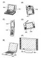
본 실시형태에서는, 본 발명의 반도체장치를 가지는 전자기기의 구체예에 대하여 설명한다. 본 실시형태에서는, 실시형태 2 및 실시형태 3에서 나타내는 표시장치를 표시부에 가지는 전자기기에 대하여 설명한다. 이러한 전자기기로서, 예를 들면, 텔레비전 장치(간단히 텔레비전 또는 텔레비전 수상기라고도 부른다), 디지털 카메라, 디지털 비디오 카메라 등의 카메라, 휴대 전화장치(간단히 휴대 전화기 또는 휴대 전화라고도 부른다), PDA 등의 휴대형 정보 단말기, 휴대형 게임기, 컴퓨터용 모니터, 컴퓨터, 카 오디오 등의 음향 재생 장치, 가정용 게임기 등의 기록 매체를 구비한 화상 재생 장치 등을 들 수 있다. 또한, 철도 역이나 공항 등의 정보 표시판이나, 거리에 있는 광고 표시판 등도 들 수 있다.In this embodiment, a specific example of an electronic apparatus having the semiconductor device of the present invention will be described. In this embodiment, an electronic apparatus having a display unit according to the second embodiment and the third embodiment in the display unit will be described. Examples of such electronic devices include portable devices such as a television device (simply referred to as a television or a television receiver), a camera such as a digital camera and a digital video camera, a mobile phone device (simply referred to as a mobile phone or a mobile phone) A portable game machine, a monitor for a computer, a sound reproduction device such as a computer and a car audio, and an image reproduction device having a recording medium such as a home game machine. In addition, information boards such as railway stations and airports, and advertising signs on the street are also included.
이하, 도 8(A)∼도 8(F)를 참조하여, 전자기기의 구체예에 대하여 설명한다. 도 8(A)∼도 8(F)는 전자기기의 외관도이다.Hereinafter, specific examples of the electronic apparatus will be described with reference to Figs. 8 (A) to 8 (F). 8 (A) to 8 (F) are external views of electronic equipment.
도 8(A)에 나타내는 휴대형 정보 단말기는 본체(9201), 표시부(9202) 등을 구비하고 있다. 표시부(9202)에, 실시형태 2 및 실시형태 3에서 나타내는 표시장치를 적용함으로써, 고정세한 표시가 가능한 휴대형 정보 단말기를 싼값으로 제공할 수 있다.The portable information terminal shown in Fig. 8A includes a
도 8(B)에 나타내는 디지털 비디오 카메라는 표시부(9701), 표시부(9702) 등을 구비하고 있다. 표시부(9701)에 실시형태 2 및 실시형태 3에서 나타내는 표시장치를 적용함으로써, 고정세한 표시가 가능한 디지털 비디오 카메라를 싼값으로 제공할 수 있다.The digital video camera shown in Fig. 8B includes a
도 8(C)에 나타내는 휴대 전화기는 본체(9101), 표시부(9102) 등을 구비하고 있다. 표시부(9102)에 실시형태 2 및 실시형태 3에서 나타내는 표시장치를 적용함으로써, 신뢰성이 높은 휴대 전화기를 싼값으로 제공할 수 있다.The cellular phone shown in Fig. 8 (C) has a
도 8(D)에 나타내는 휴대형 텔레비전 장치는 본체(9301), 표시부(9302) 등을 구비하고 있다. 표시부(9302)에 실시형태 2 및 실시형태 3에서 나타내는 표시장치를 적용함으로써, 고정세한 표시가 가능한 휴대형 텔레비전 장치를 싼값으로 제공할 수 있다.A portable television apparatus shown in Fig. 8D includes a
도 8(E)에 나타내는 휴대형 컴퓨터는 본체(9401), 표시부(9402) 등을 구비하고 있다. 그 표시부(9402)에, 실시형태 2 및 실시형태 3에서 나타내는 표시장치를 적용함으로써, 고화질의 표시가 가능한 휴대형 컴퓨터를 싼값으로 제공할 수 있다.The portable computer shown in Fig. 8 (E) has a
도 8(F)에 나타내는 텔레비전 장치는 본체(9501), 표시부(9502) 등을 구비하 고 있다. 표시부(9502)에 실시형태 2 및 실시형태 3에서 나타내는 표시장치를 적용함으로써, 고정세한 표시가 가능한 텔레비전 장치를 싼값으로 제공할 수 있다.A television device shown in Fig. 8 (F) has a
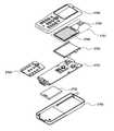
여기서, 도 8(C)의 휴대 전화기의 보다 구체적인 구성을 도 9를 사용하여 설명한다. 도 9는 휴대 전화기의 분해도이다.Here, a more specific configuration of the cellular phone of Fig. 8 (C) will be described with reference to Fig. 9 is an exploded view of a mobile phone.
도 9에 나타내는 바와 같이, 휴대 전화기는, 케이스(2700, 2706), 패널(2701), 하우징(2702), 프린트 배선 기판(2703), 조작 버튼(2704), 배터리(2705)를 가진다. 패널(2701)은 하우징(2702)에 탈착할 수 있도록 조립되고, 하우징(2702)은 프린트 배선 기판(2703)에 설치된다. 하우징(2702)은 패널(2701)이 내장되는 전자기기에 맞추어, 형상이나 치수가 적절히 변경된다.As shown in Fig. 9, the mobile phone has a
프린트 배선 기판(2703)에는 패키징된 복수의 반도체장치가 실장되어 있고, 이들 중 하나로서 본 발명의 반도체장치를 사용할 수 있다. 프린트 배선 기판(2703)에 실장되는 복수의 반도체장치는 콘트롤러, 중앙 처리 유닛(CPU : Central Processing Unit), 메모리, 전원 회로, 음성 처리 회로, 송수신 회로 등의 어느 기능을 가진다.A plurality of packaged semiconductor devices are mounted on the printed
패널(2701)은 접속 필름(2708)을 통하여 프린트 배선 기판(2703)에 접속된다. 상기 패널(2701), 하우징(2702), 프린트 배선 기판(2703)은, 조작 버튼(2704) 및 배터리(2705)와 함께 케이스(2700, 2706) 내부에 수납되고, 패널(2701)이 포함하는 화소 영역(2709)은, 케이스(2700)에 형성된 개구창을 통하여 시인(視認)할 수 있도록 배치된다. 패널(2701)에 실시형태 2 및 실시형태 3의 표시장치가 사용된다.The
다음에, 도 10을 사용하여, 도 8(D) 및 도 8(F)에 나타내는 텔레비전 장치의 구성예를 설명한다. 도 10은 텔레비전 장치의 주요한 구성을 나타내는 블록도이다.Next, a configuration example of the television apparatus shown in Figs. 8 (D) and 8 (F) will be described with reference to Fig. 10 is a block diagram showing the main configuration of the television apparatus.
튜너(9511)는 영상 신호와 음성 신호를 수신한다. 영상 신호는 영상 검파 회로(9512)와, 그 영상 검파 회로(9512)로부터 출력되는 신호를 적색, 녹색, 청색의 각 색에 대응한 색 신호로 변환하는 영상 신호 처리 회로(9513)와, 그 영상 신호를 드라이버 IC의 입력 사양으로 변환하는 제어 회로(9514)에 의하여 처리된다.The
제어 회로(9514)는, 표시 패널(9515)의 주사선 구동회로(9516) 및 신호선 구동회로(9517) 각각에 신호를 출력하는 회로이다. 또한, 디지털 구동하는 경우에는, 제어 회로(9514)의 신호선 구동회로(9517)에의 출력측에 신호 분할 회로(9518)를 마련하여, 입력 디지털 신호를 m개로 분할하여 공급하는 구성으로 할 수 있다.The
튜너(9511)에서 수신한 음성 신호는 음성 검파 회로(9521)로 보내지고, 그의 출력은 음성 신호 처리회로(9522)를 거쳐 스피커(9523)에 공급된다. 제어 회로(9524)는 수신국(수신 주파수)이나 음량 등의 제어 정보를 입력부(9525)로부터 받아서, 튜너(9511)나 음성 신호 처리 회로(9522)에 그 신호를 출력한다.The audio signal received by the
[실시형태 5][Embodiment 5]
본 실시형태에서는, 비접촉으로 데이터의 전송이 가능한 반도체장치에 대하여 설명한다.In the present embodiment, a semiconductor device capable of data transmission in a noncontact manner will be described.
먼저, 도 11를 참조하여, 비접촉으로 데이터의 전송이 가능한 반도체장치의 구성을 설명한다. 도 11은, 비접촉으로 데이터의 전송이 가능한 반도체장치의 구 성예를 나타내는 블록도이다. 본 실시형태의 반도체장치는, 크게 나눠서, 안테나부(2001), 전원부(2002), 로직(logic)부(2003)로 구성된다.First, the structure of a semiconductor device capable of data transmission in a noncontact manner will be described with reference to FIG. 11 is a block diagram showing a configuration example of a semiconductor device capable of data transmission in a noncontact manner. The semiconductor device of the present embodiment is largely divided into an
안테나부(2001)는 외부 신호의 수신과 데이터의 송신을 행하기 위한 안테나(2011)로 이루어지고, 또한, 반도체장치에서의 신호 전송 방식은 전자(電磁) 결합 방식, 전자 유도 방식, 또는 마이크로파 방식 등을 사용할 수 있다. 또한, 그 전송 방식은 실시자가 사용 용도를 고려하여 적절히 선택하고, 전송 방식에 최적인 안테나가 마련된다.The
전원부(2002)는 정류 화로(2021), 보유 용량(2022), 및 정전압 회로(2023)로 이루어진다. 정류 회로(2021)는 안테나부(2001)에서 수신된 전파로부터 전압을 만드는 회로이다. 보유 용량(2022)은 정류 회로(2021)에서 생성된 전압을 보유하기 위한 회로이다. 정전압 회로(2023)은 정류 회로(2021)에서 생성된 전압을 일정한 크기로 하기 위한 회로이다.The
로직부(2003)는, 수신한 신호를 복조하는 복조 회로(2031)와, 클록 신호를 생성하는 클록 생성/보정 회로(2032)와, 각 코드 인식 및 판정 회로(2033)와, 메모리로부터 데이터를 판독하기 위한 신호를 수신 신호에 의거하여 만들어 내는 메모리 컨트롤러(2034)와, 부호화된 신호를 수신 신호로 변환하기 위한 변조 회로(2035)와, 판독한 데이터를 부호화하는 부호화 회로(2037)와, 데이터를 보유하는 마스크 ROM(2038)을 포함한다. 또한, 변조 회로(2035)는 변조용 저항(2036)을 가진다.The
각 코드 인식 및 판정 회로(2033)가 인식 및 판정하는 코드는 프레임 종료 신호(EOF : End Of Frame), 프레임 개시 신호(SOF : Start Of Frame), 플래그(flag), 코맨드 코드, 마스크 길이(mask length), 마스크 값(mask value) 등이다. 또한, 각 코드 인식 및 판정 회로(2033)는 송신 에러를 식별하는 순회 용장 검사(CRC : Cyclic Redundancy Check) 기능도 포함한다.The codes that are recognized and determined by each code recognition and
다음에, 도 12∼도 15를 참조하여, 안테나부(2001), 전원부(2002), 및 로직부(2003)를 가지는 반도체장치의 제작방법을 설명한다. 도 12∼도 15는 본 실시형태의 반도체장치의 제작방법을 설명하기 위한 단면도이다. 또한, 도 12∼도 15에서, 전원부(2002) 및 로직부(2003)로서 대표적으로 박막트랜지스터를 도시한다. 전원부(2002) 및 로직부(2003)에는, 박막트렌지스터 이외에, 다이오드, 저항 소자, 용량 소자 또는 기억 소자 등 회로의 기능에 따라 각종의 반도체 소자가 형성된다.Next, a method of manufacturing a semiconductor device having the
또한, 본 실시형태에서는, 반도체장치의 제작방법으로서, 반도체 소자를 기판 위에 제작한 후, 제작시에 사용한 기판을 반도체 소자로부터 박리하고, 반도체 소자를 다른 기판에 전치(轉置)하는 기술에 대하여 설명한다. 이 기술을 적용함으로써, 본 실시형태의 반도체장치뿐만 아니라, 실시형태 2 및 실시형태 3에서 설명한 표시장치 등 다른 반도체장치를 제작할 수도 있다.In the present embodiment, as a method of manufacturing a semiconductor device, there is a technique of manufacturing a semiconductor element on a substrate, peeling the substrate used in the manufacture from the semiconductor element, and transferring the semiconductor element to another substrate Explain. By applying this technique, not only the semiconductor device of the present embodiment but also other semiconductor devices such as the display device described in
먼저, 도 12(A)에 나타내는 바와 같이, 기판(400)을 준비한다. 기판(400)에는 금속 기판이나 스테인리스 기판의 일 표면에 절연막을 형성한 기판, 본 공정의 처리 온도에 견딜 수 있는 내열성이 있는 플라스틱 기판 등을 사용할 수 있지만, 여기서는, 기판(400)으로서 유리 기판을 사용한다.First, as shown in Fig. 12 (A), a
다음에, 하지가 되는 절연막(401)을 형성하기 전에, 기판(400) 위에 박리 막(402)을 형성한다. 박리막(402)에 박리를 생기게 함으로써, 기판(400)을 반도체 소자로부터 분리한다.Next, a
박리막(402)은, 텅스텐(W), 몰리브덴(Mo), 티탄(Ti), 탄탈(Ta), 니오브(Nb), 니켈(Ni), 코발트(Co), 지르코늄(Zr), 아연(Zn), 루테늄(Ru), 로듐(Rh), 팔라듐(Pd), 오스뮴(Os), 이리듐(Ir), 규소(Si)로부터 선택된 원소로 이루어지는 재료, 이들 원소를 주성분으로 하는 합금 재료, 및 이들 원소를 주성분으로 하는 화합물 재료로부터 선택된 재료로 이루어지는 단층막 또는 적층막으로 형성된다. 또한, 규소를 함유하는 층의 결정 구조는 비정질, 미(微)결정, 다결정의 어느 경우라도 좋다. 이들 재료로 이루어지는 막은 스퍼터링법이나 플라즈마 CVD법, 도포법, 인쇄법 등에 의하여 형성할 수 있다.The
상기 박리막(402)이 단층 구조인 경우에는, 바람직하게는, 텅스텐층, 몰리브덴층, 또는 텅스텐과 몰리브덴의 혼합물을 포함하는 층을 형성한다. 또는 텅스텐과 몰리브덴의 혼합물이란, 예를 들면, 텅스텐과 몰리브덴의 합금에 상당하다. 또는, 단층의 박리막(402)에 화합물 재료를 사용하는 경우에는, 텅스텐 산화물, 텅스텐 산화질화물, 몰리브덴 산화물, 몰리브덴 산화질화물, 텅스텐 산화물과 몰리브덴 산화물의 혼합물, 또는 텅스텐 산화질화물과 몰리브덴 산화질화물의 혼합물이 바람직하다.When the
상기 박리막(402)이 적층 구조인 경우에는, 바람직하게는, 첫번째 층에, 텅스텐층, 몰리브덴층, 또는 텅스텐과 몰리브덴의 혼합물로 이루어지는 층 중의 어느 것을 형성한다. 두번째 층에, 텅스텐층, 몰리브덴층, 텅스텐 또는 몰리브덴의 산 화물층, 텅스텐 또는 몰리브덴의 질화물층, 텅스텐 또는 몰리브덴의 산화질화물층, 텅스텐 산화물과 몰리브덴 산화물의 혼합물로 이루어지는 층 중의 어느 것을 형성한다.When the
상기 박리막(402)으로서, 텅스텐층과 텅스텐 산화물층의 적층막을 형성하기 위해서는, 텅스텐층을 형성하고, 그의 상층에 산화물로 이루어지는 절연막(대표적으로는, 산화규소막)을 형성함으로써, 텅스텐층과 절연층과의 계면에, 텅스텐의 산화물을 함유하는 층이 형성되는 것을 이용할 수 있다. 이 방법을 이용하여, 두번째 층에 질화물 또는 산화질화물을 형성하는 경우에는, 텅스텐을 함유하는 층을 형성한 후, 그의 상층에 질화규소층, 산화질화규소층 또는 질화산화규소층을 형성하면 좋다.In order to form a laminated film of the tungsten layer and the tungsten oxide layer as the
또는, 텅스텐층의 표면에, 열산화 처리, 산소 플라즈마 처리, N2O 플라즈마 처리, 오존수 등의 산화력이 강한 용액을 사용한 처리, 수소가 첨가된 물을 사용한 처리 등을 행하여, 텅스텐 산화물층을 형성할 수도 있다.Alternatively, a tungsten oxide layer is formed on the surface of the tungsten layer by a thermal oxidation treatment, an oxygen plasma treatment, an N2 O plasma treatment, a treatment using a strong oxidizing power such as ozone water, a treatment using hydrogenated water, You may.
이상의 형성 방법은, 박리막(402)으로서, 몰리브덴층과, 산화물 등의 몰리브덴 화합물로 이루어지는 층의 적층막을 형성하는 경우에도 적용할 수 있다.The above-described forming method can also be applied to a case where a laminated film of a molybdenum layer and a layer of a molybdenum compound such as an oxide is formed as the
또한, 텅스텐의 산화물은 WOx로 표시된다. 본 실시형태의 경우, x는 2 ≤ x ≤ 3의 범위내이며, x가 2인 경우(WO2), x가 2.5인 경우(W2O5), x가 2.75인 경우(W4O11), x가 3인 경우(WO3) 등이 있다.Further, the oxide of tungsten is represented by WOx . In the case of this embodiment, x is 2 ≤ x ≤ 3 range and the, when x is2 (WO 2), if (W2 O5), x is 2.75 when x is 2.5 (W4 O11 ), x is 3 (WO3 ), and the like.
본 실시형태의 박리막(402) 및 절연막(401)의 형성방법으로서, 여기서는, 스 퍼터링법에 의하여 두께 20 nm∼100 nm, 바람직하게는 40 nm∼80 nm의 텅스텐막을 형성한다. 그 후, N2O 가스를 흘리면서 플라즈마를 발생시켜 박리막(402)의 표면을 산화시키고, 산화텅스텐막을 형성한다. 그 후, 플라즈마 CVD법에 의하여 질화산화규소막과 산화질화규소막의 적층막을 형성한다. 이 적층막이 하지 절연막(401)이다.As a method of forming the
다음에, 실시형태 1 및 실시형태 2와 미찬가지로, 박리막(402) 위에 절연막(401)을 형성하고, 이 절연막(401) 위에 박막트랜지스터(404)를 형성한다. 박막트랜지스터(404)는 실시형태 2에서 설명한 박막트랜지스터 제작방법을 사용할 수 있고, 실시형태 2의 박막트랜지스터(225∼227)와 마찬가지로 형성할 수 있다.Next, an insulating
이어서, 그 박막트랜지스터(404)를 덮는 층간절연막(405)을 형성하고, 층간절연막(405) 위에 박막트랜지스터(404)에 전기적으로 접속하는 배선(406)을 형성한다. 배선(406)은, 예를 들면, 실시형태 2에서 나타내는 배선(234∼239)과 마찬가지로 형성할 수 있다. 다음에, 배선(406)을 덮는 절연막(407)을 형성하고, 이 절연막(407) 위에 배선(406)에 접속하는 도전막(408)을 형성한다.Next, an
층간절연막(405) 및 절연막(407)은 수지 재료로 형성할 수 있다. 예를 들면, 폴리이미드, 아크릴, 또는 실록산 폴리머를 도포하고 소성하여 형성할 수 있다. 또한, 스퍼터링법이나 플라즈마 CVD법, 도포법, 인쇄법 등에 의하여, 무기 화합물을 사용하여 단층 또는 적층으로 형성하여도 좋다. 그 무기 화합물의 대표예로서는, 산화규소, 질화규소, 산화질화규소, 질화산화규소가 있다.The
다음에, 도 12(B)에 나타내는 바와 같이, 도전막(408) 위에 도전막(411)을 적층하여 형성한다. 여기서는, 인쇄법에 의하여 금 입자를 함유하는 조성물을 인쇄하고, 200℃에서 30분간 가열함으로써 조성물을 소성하여 도전막(411)을 형성한다. 또한, 증착법이나 스퍼터링법을 사용하여 도전막을 형성하고, 에칭에 의하여 소망의 형상으로 가공함으로써, 도전막(411)을 형성할 수도 있다.Next, as shown in Fig. 12B, a
이어서, 도 12(C)에 나타내는 바와 같이, 절연막(407) 위에 막 두께 1 ㎛∼20 ㎛, 바람직하게는 5 ㎛∼10 ㎛의 절연막(412)을 형성한다. 여기서는, 절연막(412)을 에폭시 수지를 사용하여 형성한다. 그 형성시에는, 에폭시 수지의 조성물을 함유하는 용액을 스핀 코팅법에 의하여 도포하고, 160℃에서 30분간 가열하여 용액을 경화시켜 에폭시 수지를 경화시킨다. 그 후, 도전막(411)을 덮는 부분의 에폭시 수지를 제거하여, 도전막(411)의 상면을 노출시키는데, 도전막(408) 및 도전막(411)의 주위가 에폭시 수지에 덮여 있도록 한다.Then, as shown in Fig. 12 (C), an insulating
여기서는, 절연막(401)으로부터 절연막(412)까지의 적층체를 소자 형성층(410)으로 한다.Here, a layered body from the insulating
다음에, 도 12(D)에 나타내는 바와 같이, 후의 박리 공정을 용이하게 행하기 위하여, 레이저 빔(413)을 절연막(401, 405, 407, 412)에 조사하여, 도 12(E)에 나타내는 바와 같은 개구부(414)를 형성한다. 레이저 빔(413)을 조사함으로써, 절연막(401, 405, 407, 412)이 레이저 빔(413)을 흡수하여 용융하여 개구부(414)가 형성된다. 개구부(414)는 기판(400)의 주위를 둘러싸도록 형성된다. 개구부(414)를 형성한 후, 절연막(412)에 점착 부재(415)를 부착시킨다. 또한, 개구부(414)를 형 성하지 않아도, 소자 형성층(410)을 기판(400)으로부터 용이하게 분리할 수 있는 경우에는, 레이저 빔(413)의 조사를 생략할 수 있다.12 (D), the
다음에, 박리막(402) 및 절연막(401)의 계면에 형성되어 있는 금속 산화물층(여기서는, 텅스텐 산화물층)에서 박리를 생기게 하고, 도 13(A)에 나타내는 바와 같이, 기판(400)으로부터 소자 형성층(410)을 분리한다. 이 공정에서, 점착 부재(415)는, 기판(400)으로부터 분리된 소자 형성층(410)을 지지하기 위한 지지부재로서 기능한다.Next, peeling is caused in the metal oxide layer (here, tungsten oxide layer) formed at the interface between the
박리층(402)에 형성되어 있는 텅스텐 산화물층은 깨지기 쉽기 때문에, 역학적인 힘을 가함으로써 박리가 생기고, 소자 형성층(410)을 기판(400)으로부터 분리할 수 있다. 소자 형성층(410)을 기판(400)으로부터 분리하는 방법으로서, 대표적으로는, 사람의 손이나 그립 툴(grip tool)를 사용하여 소자 형성층(410)을 박리하는 방법, 롤러를 가지는 박리 장치를 사용하는 방법 등이 있다.Since the tungsten oxide layer formed on the
또한, 본 실시형태에서는, 소자 형성층(410)과 기판(400)을 분리하기 위하여, 박리막(402)을 형성하는 방법을 사용하였지만, 박리막(402)을 형성하지 않는 방법을 사용할 수도 있다. 예를 들면, 도 12(E)의 공정 후, 기판(400)을 기계적으로 연삭 및 연마하여 제거하는 방법이나, 기판(400)을 HF 등의 용액을 사용하여 용해하는 방법을 사용할 수도 있다.Although the method of forming the
다음에, 도 13(B)에 나타내는 바와 같이, 소자 형성층(410)의 절연막(401)에 가요성 기판(422)을 부착한 후, 점착 부재(415)를 소자 형성층(410)으로부터 박리한다. 여기서는, 가요성 기판(422)으로서, 캐스트(cast)법에 의하여 폴리아닐린으 로 형성된 필름을 사용한다.13B, after the
그 후, 도 13(C)에 나타내는 바와 같이, 가요성 기판(422)을 다이싱(dicing) 프레임(432)의 UV 시트(431)에 부착한다. UV 시트(431)는 점착성을 가지기 때문에, UV 시트(431) 위에 가요성 기판(422)이 고정된다. 그 후, 도전막(411)에 레이저 빔을 조사하여, 도전막(411)과 도전막(408) 사이의 밀착성을 높여도 좋다.13 (C), the
이어서, 도 13(D)에 나타내는 바와 같이, 도전막(411) 위에 접속 단자(433)를 형성한다. 이 접속 단자(433)를 형성함으로써, 후에 안테나로서 기능하는 도전막과의 위치맞춤 및 소자 형성층(410)과의 전기적 접속을 용이하게 행할 수 있다.Then, as shown in Fig. 13D, a
다음에, 도 14(A)에 나타내는 바와 같이, 소자 형성층(410) 및 가요성 기판(422)에 레이저 빔(434)을 조사하여, 도 14(B)에 나타내는 바와 같이, 소자 형성층(410)을 복수로 분단한다. 이것은, 1장의 기판(400) 위에, 반도체장치를 구성하는 복수의 회로가 형성되어 있기 때문에, 소자 형성층(410)을 하나의 장치마다 분할하기 위한 공정이다. 또한, 소자 형성층(410)의 분할에 레이저 컷법을 사용하였지만, 다이싱법, 스크라이빙법 등을 사용할 수 있다. 또한, 여기서는, 장치마다 분단된 소자 형성층(410)을 박막 집적회로라고 한다. 또한, 도 14(B)에는, 소자 형성층(410)을 2개의 박막 집적회로(442a, 442b)로 분할한 예를 나타내고 있지만, 박막 집적회로의 개수는 2개로 한정되지 않는다.14A, the element-formed
다음에, 다이싱 프레임(432)의 UV 시트(431)에 UV광을 조사하여, UV 시트(431)의 점착력을 저하시킨 후, UV 시트(431)를 익스팬더(expander) 프레임(444)으로 지지한다. 이 때, UV 시트(431)를 늘린 상태로 익스팬더 프레임(444)으로 지 지한다. 그 결과, 도 14(C)에 나타내는 바와 같이, 박막 집적회로(442a, 442b)들 사이에 형성된 홈(441)의 폭을 확대할 수 있다. 또한, 확대된 홈(446)은, 후에 박막 집적회로(442a, 442b)에 부착되는 안테나 기판의 크기에 맞추는 것이 바람직하다.The
다음에, 안테나 기판(457)을 준비한다. 안테나 기판(457)은, 가요성 기판(456)과, 가요성 기판(456) 위에 형성된 안테나로서 기능하는 도전막(452a, 452b)과, 이 도전막(452a, 452b)을 봉지(封止)하는 절연막(453)으로 된다. 또한, 가요성 기판(456)에는, 박막 집적회로에 대응하여, 안테나로서 기능하는 도전막이 형성되어 있고, 또한 안테나로서 기능하는 도전막의 일부가 노출하도록, 개구부가 형성되어 있다.Next, the
그리고, 이방성 도전 접착제(455a, 455b)를 사용하여, 안테나 기판(457)을 박막 집적회로(442a, 442b)에 부착시킨다. 이 결과, 도 15(A)에 나타내는 바와 같이, 도전막(452a, 452b)이 각각, 박막 집적회로(442a, 442b)의 접속 단자(433)에, 이방성 도전 접착제(455a, 455b)에 함유되는 도전성 입자(454a, 454b)에 의하여 전기적으로 접속된다.Then, the
다음에, 도 15(B)에 나타내는 바와 같이, 도전막(452a, 452b), 및 박막 집적회로(442a, 442b)가 형성되어 있지 않은 영역에서, 안테나 기판(457)을 분단한다. 여기서는, 레이저 빔(461)을 사용한 레이저 컷법에 의하여 분단을 행한다. 이상의 공정에 의하여, 도 15(C)에 나타내는 바와 같이, 비접촉으로 데이터의 전송이 가능한 반도체장치(462a, 462b)를 제작할 수 있다.Next, as shown in Fig. 15B, the
또한, 소자 형성층(410) 및 안테나 기판(457)의 분할은 다음과 같이 행하여도 좋다. 이방성 도전 접착제(455a, 455b)를 사용하여 안테나 기판(457)을 박막 집적회로(442a, 442b)에 부착시킨 상태에서(도 15(A)의 상태에서), 박막 집적회로(442a, 442b)를 봉지하도록 가요성 기판(463)을 설치한다. 이어서, 레이저 컷법을 사용하여 안테나 기판(457)을 분할함으로써, 도 15(D)에 나타내는 바와 같은 박막 집적회로가 가요성 기판(463)에 봉지되어 있는 반도체장치(464)가 제작될 수 있다. 도 15(D)의 반도체장치(464)에서는, 가요성 기판(463)과 안테나 기판(457)의 가요성 기판(456)에 의하여, 박막 집적회로가 봉지되기 때문에, 도 15(C)의 반도체장치(462a, 462b)보다도 박막 집적회로의 열화를 억제하는 효과가 높다.Further, the element-formed
이상의 공정에 의하여, 박형 및 경량이며, 휠 수 있는 반도체장치를 제작할 수 있다. 또한, 반도체장치의 박막트랜지스터의 반도체층(특히, 채널 형성 영역)의 결정의 면 방위가 일치되어 있기 때문에, 박막트랜지스터의 전기 특성의 편차를 억제할 수 있다. 따라서, 고성능이며 신뢰성이 높은 반도체장치를 제작할 수 있다.By the above process, a semiconductor device which is thin and light in weight and can be manufactured can be manufactured. Further, since the plane orientations of the crystals of the semiconductor layer (particularly, the channel forming region) of the thin film transistor of the semiconductor device are matched, deviation of the electric characteristics of the thin film transistor can be suppressed. Therefore, a semiconductor device having high performance and high reliability can be manufactured.
다음에, 비접촉으로 데이터 전송이 가능한 상기 반도체장치의 용도에 대하여 도 16(A)∼도 16(F)를 사용하여 설명한다.Next, the use of the semiconductor device capable of data transmission in a noncontact manner will be described with reference to Figs. 16 (A) to 16 (F).
본 실시형태의 반도체장치(500)는 물품의 표면에 고정하거나 물픔에 묻는 등의 방법으로 사용된다. 예를 들면, 책 등의 종이가 사용되는 물품이라면, 반도체장치(500)를 종이에 묻거나, 섞어서 뜬다. 유기 수지로 이루어지는 패키지라면, 그 유기 수지에 반도체장치(500)를 묻어서, 전자기기 등의 프린트 기판에 실장한 다.The
도 16(A)는 본 실시형태의 반도체장치(500)를 사용한 ID 라벨의 구성예를 나타내는 도면이다. 라벨 대지(501)(세퍼레이트지) 위에 복수의 ID 라벨(502)이 형성되어 있다. 각 ID 라벨(502)은, 무선통신이 가능한 안테나와 박막 집적회로를 가지는 반도체장치(500)를 내포하고 있다. ID 라벨(502)은 박스(503)에 수납된다. ID 라벨(502)에는 그 상품이나 역무에 관한 정보(상품명, 브랜드, 상표, 상표권자, 판매자, 제조자 등)가 기재된다. 한편, 내장되어 있는 반도체장치(500)의 박막 집적회로에는, 그 상품(또는 상품의 종류) 고유의 ID 넘버가 기억된다. 반도체장치(500)의 집적회로에는, ID 라벨(502)의 표면에 명기할 수 없는 막대한 정보, 예를 들면, 상품의 산지, 판매지, 품질, 원재료, 효능, 용도, 수량, 형상, 가격, 생산방법, 사용방법, 생산 시기, 사용 시기, 상미(賞味) 기한, 취급 설명, 상품에 관한 지적재산 정보 등이 기억된다.16A is a diagram showing a configuration example of an ID label using the
도 16(B)는 ID 태그(tag)(504)의 구성예를 나타내는 도면이다. ID 태그(504)에는, 종이나 플라스틱의 태그에 반도체장치(500)를 내장하고 있다. 무선 통신이 가능한 ID 태그(504)를 상품에 설치함으로써, 상품의 유통 경로를 더듬을 수 있기 때문에 상품관리가 용이해진다.Fig. 16B is a diagram showing an example of the configuration of an ID tag (tag) 504. Fig. In the
도 16(C)는 ID 카드(505)의 구성예를 나타내는 도면이다. ID 카드(505)는, 2장의 플라스틱 카드 사이에 반도체장치(500)가 끼워져 있다. ID 카드(505)로서는, 캐시 카드, 크레디트 카드, 프리페이드 카드, 전자승차권, 전자 머니, 전화 카드, 회원 카드 등의 모든 카드류가 포함된다.Fig. 16C is a diagram showing an example of the configuration of the
도 16(D)에는, 종이에 반도체장치(500)를 내포한 물품의 구성예를 나타내고, 그 물품의 구체예로서, 무기명 채권(506)을 나타낸다. 무기명 채권(506)에는, 반도체장치(500)가 매립되어 있다. 무기명 채권류(507)에는, 우표, 차표, 티킷, 입장권, 상품권, 도서권, 문구권, 맥주권, 쌀상품권, 각종 기프트권, 각종 서비스권 등이 포함된다.Fig. 16D shows a structural example of an article containing a
또한, 도 16(B)에 나타내는 ID 태그(504)를 물품에 설치하는 대신에, 물품에 반도체장치(500)를 설치할 수도 있다. 포장지, 포장 박스, 병 등의 포장용 자재 또는 곤포(梱包)용 자재(예를 들면, 도 16(E)의 병(507) 참조), 자전거, 자동 이륜차 등의 탈 것류(도 16(F)의 자전거(508) 참조), 신변용품, 식품류, 의류, 생활용품류, 전자기기 등에 본 실시형태의 반도체장치(500)를 설치함으로써, 검품 시스템 등의 효율을 높일 수 있다.Instead of providing the
[실시예 1][Example 1]
본 실시예에서는, 폭이 2 ㎛ 이하인 선형 레이저 빔을 얻기 위한 비구면 실린드리컬 렌즈에 대하여 설명한다.In this embodiment, an aspherical cylindrical lens for obtaining a linear laser beam having a width of 2 m or less will be described.
비구면 실린드리컬 렌즈를 설계하기 위하여, 빔 스폿을 직경 2 ㎛의 원 형상으로 집광할 수 있는 회전 대칭 비구면 렌즈를 설계하였다. 회전 대칭 비구면 렌즈의 광학 설계에는, 범용적인 광학 설계 소프트웨어의 하나인 "ZEMAX"(ZEMAX Development Corporation사제)를 사용하였다. 렌즈의 서피스 타입(surface type)은, ZEMAX를 사용하여 준비된 우수차(偶數次)(even-ordered) 비구면(even surface)을 사용하였다. 우수차 비구면은, 코닉 상수(conic constant)를 사용하여 기술되 는 비구면을 베이스로 사용하여, 반경 좌표(r)의 우수차 다항식으로 기술된다. 그 면의 새그(sag)(d)는 하기의 식 (1)로 기술된다.In order to design an aspherical cylindrical lens, a rotationally symmetric aspherical lens which can focus the beam spot into a circular shape with a diameter of 2 ㎛ is designed. In optical design of rotationally symmetric aspherical lens, "ZEMAX" (manufactured by ZEMAX Development Corporation), which is one of general optical design software, was used. The surface type of the lens used an even-ordered even surface prepared using ZEMAX. The asymmetric aspheric surface is described by an excellent difference polynomial of the radial coordinate (r) using an aspheric surface described using a conic constant as a base. The sag (d) of the surface is described by the following equation (1).

상기 식 (1)에서, c는 곡률반경의 역수이고, k는 코닉 정수이고, r는 구면의 반경이고, α1, α2, α3, ....,α8은 비구면 계수이다.Where c is a reciprocal of the radius of curvature, k is a conic constant, r is the radius of the spherical surface, and?1 ,?2 ,?3, ..., ?8 are aspheric coefficients.
본 실시예에서는, 상기 식 (1)에서, r의 6차 이상의 비구면 계수 α3, α4, α5, ..., α8을 제로(0)로 하고, 다항식의 제1항 내지 제3항만을 사용하였다.In this embodiment, it is assumed that the aspheric coefficients?3 ,?4 ,?5, ...,?8 of the sixth or higher order of r in the formula (1) The port was used.
도 17∼도 21은 회전 대칭 비구면 렌즈를 설계하였을 때의 ZEMAX의 윈도 화면이다. 도 17은 상기 식 (1)의 파라미터의 입력 화면이고, 회전 대칭 비구면 렌즈의 렌즈 데이터가 나타내어져 있다. 도 18은 회전 대칭 비구면 렌즈의 회전 중심축을 포함하는 면에서 절단한 단면도를 나타내는 화면이다. 도 18에 나타내는 바와 같이, 설계한 회전 대칭 비구면 렌즈는 평볼록 렌즈이다.17 to 21 are ZEMAX window screens when a rotationally symmetric aspheric lens is designed. 17 is an input screen of the parameters of the above equation (1), and lens data of a rotationally symmetric aspheric lens is shown. Fig. 18 is a view showing a cross-sectional view taken along the plane including the rotation center axis of the rotationally symmetric aspherical lens. Fig. As shown in Fig. 18, the designed rotationally symmetric aspheric lens is a flat convex lens.
도 19∼도 21은 스폿 다이어그램(Spot diagram)을 나타내는 화면이다. 도 19∼도 21의 스폿 다이어그램을 보면, 도 17의 렌즈 데이터에 의거하여 설계된 회전 대칭 비구면 렌즈에 의하여, 빔 스폿을 직경 2 ㎛ 이하로 집광할 수 있다는 것을 알 수 있다.19 to 21 are screens showing a spot diagram. It can be seen from the spot diagrams of Figs. 19 to 21 that the beam spot can be condensed to a diameter of 2 mu m or less by the rotationally symmetric aspherical lens designed based on the lens data of Fig.
도 17의 렌즈 데이터로 기술되는 곡면을 가지는 회전 대칭 비구면 렌즈는 구 면 수차가 매우 작기 때문에, 빔 스폿을 직경 2 ㎛ 이하로 집광할 수 있다. 따라서, 도 17의 렌즈 데이터로 기술되는 회전 대칭 비구면을 기초로, 한축 방향만으로 굴절률을 가지는 회전 대칭 비구면 실린드리컬 렌즈를 설계함으로써, 빔 스폿을 폭 2 ㎛ 정도의 매우 가는 선 형상으로 집광하는 렌즈를 제작할 수 있다.Since the rotationally symmetric aspherical lens having a curved surface described by the lens data in Fig. 17 has a very small spherical aberration, the beam spot can be condensed to a diameter of 2 mu m or less. Therefore, by designing a rotationally symmetric aspherical cylindrical lens having a refractive index only in one axial direction on the basis of the rotationally symmetric aspheric surface described by the lens data in Fig. 17, it is possible to provide a lens for condensing the beam spot into a very thin linear shape with a width of about 2 [ .
또한, 도 17의 렌즈 데이터에 의거하여 설계되는 회전 대칭 비구면 실린드리컬 렌즈는 초점 심도가 ±2 ㎛ 정도가 된다. 그래서, 이 초점 심도의 범위보다도 표면 거치름(roughness)이 큰 반도체막을 결정화하는 경우에는, 오토포커스 장치를 사용하여, 초점을 조절하면서 레이저 빔을 조사하는 것이 바람직하다.Further, the rotation symmetric aspherical cylindrical lens designed on the basis of the lens data in Fig. 17 has a depth of focus of about 占 퐉. Therefore, when crystallizing a semiconductor film having a larger surface roughness than the range of the depth of focus, it is preferable to irradiate the laser beam while adjusting the focus using an autofocusing apparatus.
비구면 실린드리컬 렌즈는 구면 수차가 작기 때문에, 도 19∼도 21에 나타내는 바와 같이, 비구면 실린드리컬 렌즈에 의하여 빔 폭이 2 ㎛ 이하인 매우 가는 선 형상으로 집광할 수 있다. 또한, 본 실시예의 비구면 실린드리컬 렌즈와 마찬가지로 통과하는 빔을 굴절하여, 빔을 폭이 2 ㎛ 이하인 매우 가는 선 형상으로 집광하는 굴절률 분포형 렌즈를 설계할 수도 있다. 굴절률 분포형 렌즈의 설계는 렌즈 매질의 굴절률의 구배를 결정함으로써 가능하다.Since the spherical aberration of the aspherical cylindrical lens is small, as shown in Figs. 19 to 21, the aspherical cylindrical lens can condense the light into a very thin linear shape having a beam width of 2 탆 or less. Further, as in the case of the aspherical cylindrical lens of this embodiment, it is also possible to design a refractive index distribution type lens which refracts a passing beam to condense the beam into a very thin line shape having a width of 2 m or less. The design of the refractive index distribution type lens is possible by determining the gradient of the refractive index of the lens medium.
도 1(A)∼도 1(C)는 본 발명의 반도체막 결정화 방법을 설명하는 단면도.1 (A) to 1 (C) are cross-sectional views illustrating a semiconductor film crystallization method of the present invention.
도 2는 도 1(B)에 대응하는 사시도.Fig. 2 is a perspective view corresponding to Fig. 1 (B). Fig.
도 3은 본 발명의 반도체막 결정화 방법에 사용되는 레이저 조사 장치의 구성을 나타내는 도면.3 is a view showing a configuration of a laser irradiation apparatus used in a semiconductor film crystallization method of the present invention.
도 4(A)∼도 4(D)는 본 발명에 의하여 형성된 결정성 반도체막을 사용하여 박막트랜지스터를 제작하는 방법을 성명하기 위한 단면도.4A to 4D are cross-sectional views for describing a method of manufacturing a thin film transistor using a crystalline semiconductor film formed by the present invention.
도 5(A)∼도 5(D)는 본 발명의 반도체장치 제작방법을 설명하기 위한 단면도로서, 액티브 매트릭스형 액정표시장치의 제작방법을 설명하는 단면도.5A to 5D are cross-sectional views for explaining a method for manufacturing a semiconductor device of the present invention, and are cross-sectional views for explaining a method of manufacturing an active matrix type liquid crystal display device.
도 6(A)∼도 6(C)는 도 5(D)에 계속되는 공정을 설명하기 위한 단면도.6 (A) to 6 (C) are cross-sectional views for explaining a process subsequent to that of Fig. 5 (D).
도 7(A)∼도 7(C)는 본 발명의 반도체장치 제작방법을 설명하기 위한 단면도로서, 액티브 매트릭스형 액정표시장치의 제작방법을 설명하는 단면도.FIGS. 7A to 7C are cross-sectional views for explaining a method for manufacturing a semiconductor device of the present invention, and are cross-sectional views for explaining a manufacturing method of an active matrix type liquid crystal display device. FIG.
도 8(A)∼도 8(F)는 본 발명의 반도체장치를 표시부에 가지는 전자기기의 외관도로서, 도 8(A)는 휴대형 정보 단말기, 도 8(B)는 디지털 비디오 카메라, 도 8(C)는 휴대 전화기, 도 8(D)는 휴대형 텔레비전 장치, 도 8(E)는 휴대형 컴퓨터, 도 8(F)는 텔레비전 장치.8 (A) to 8 (F) are external views of an electronic device having a semiconductor device of the present invention in a display portion. Fig. 8 (A) is a portable information terminal, Fig. 8 (C) is a portable telephone, Fig. 8 (D) is a portable television device, Fig. 8 (E) is a portable computer, and Fig. 8 (F) is a television device.
도 9는 도 8(C)의 휴대 전화기의 분해도.Fig. 9 is an exploded view of the cellular phone of Fig. 8 (C). Fig.
도 10은 도 8(D) 및 도 8(F)의 텔레비전 장치의 구성예를 나타내는 블록도.Fig. 10 is a block diagram showing a configuration example of the television apparatus of Fig. 8 (D) and Fig. 8 (F); Fig.
도 11은 본 발명의 비접촉으로 데이터 전송이 가능한 반도체장치의 블록도.11 is a block diagram of a semiconductor device capable of data transmission in a noncontact manner according to the present invention.
도 12(A)∼도 12(E)는 본 발명의 반도체장치 제작방법을 설명하기 위한 단면 도로서, 비접촉으로 데이터 전송이 가능한 반도체장치의 제작방법을 설명하는 단면도.12A to 12E are cross-sectional views illustrating a method of manufacturing a semiconductor device capable of data transmission in a noncontact manner, for explaining a method of manufacturing the semiconductor device of the present invention.
도 13(A)∼도 13(D)는 도 12(E)에 계속되는 공정을 설명하기 위한 단면도.13 (A) to 13 (D) are cross-sectional views for explaining a process subsequent to that of Fig. 12 (E).
도 14(A)∼도 14(C)는 도 13(D)에 계속되는 공정을 설명하기 위한 단면도.Figs. 14A to 14C are cross-sectional views for explaining the steps subsequent to Fig. 13D. Fig.
도 15(A)∼도 15(D)는 도 14(C)에 계속되는 공정을 설명하기 위한 단면도.Figs. 15A to 15D are cross-sectional views for explaining the steps subsequent to Fig. 14C. Fig.
도 16(A)∼도 16(F)는 본 발명의 비접촉으로 데이터 전송이 가능한 반도체장치의 용도를 설명하는 도면.16A to 16F are diagrams for explaining the use of the semiconductor device capable of data transmission in a noncontact manner according to the present invention.
도 17은 회전 대칭 비구면 렌즈의 설계에 사용하는 소프트웨어의 윈도 화면으로서, 렌즈 데이터가 나타내어진 윈도 화면.17 is a window screen of software used for designing a rotationally symmetric aspheric lens, in which lens data is shown.
도 18은 회전 대칭 비구면 렌즈의 설계에 사용하는 소프트웨어의 윈도 화면으로서, 회전 대칭 비구면 렌즈의 단면이 나타내어진 윈도 화면.Fig. 18 is a window screen of software used for designing a rotationally symmetric aspherical lens, in which a section of a rotationally symmetric aspherical lens is shown. Fig.
도 19는 회전 대칭 비구면 렌즈의 설계에 사용하는 소프트웨어의 윈도 화면으로서, 회전 대칭 비구면 렌즈의 스폿 다이어그램이 나타내어진 윈도 화면.19 is a window screen of software used for designing a rotationally symmetric aspheric lens, in which a spot diagram of a rotationally symmetric aspherical lens is shown.
도 20은 회전 대칭 비구면 렌즈의 설계에 사용하는 소프트웨어의 윈도 화면으로서, 회전 대칭 비구면 렌즈의 스폿 다이어그램이 나타내어진 윈도 화면.20 is a window screen of software used for designing a rotationally symmetric aspheric lens, in which a spot diagram of a rotationally symmetric aspherical lens is shown.
도 21은 회전 대칭 비구면 렌즈의 설계에 사용하는 소프트웨어의 윈도 화면으로서, 회전 대칭 비구면 렌즈의 스폿 다이어그램이 나타내어진 윈도 화면.21 is a window screen of a software used for designing a rotationally symmetric aspherical lens, in which a spot diagram of a rotationally symmetric aspherical lens is shown.
도 22는 본 발명자들이 개발한 반도체막 결정화 방법을 설명하기 위한 사시도.22 is a perspective view for explaining a semiconductor film crystallization method developed by the present inventors;
도 23은 본 발명자들이 개발한 반도체막 결정화 방법에서 레이저 빔의 에너 지와 반도체막의 결정 구조의 관계를 나타내는 도면.23 is a view showing the relationship between the energy of a laser beam and the crystal structure of a semiconductor film in a semiconductor film crystallization method developed by the present inventors;
<도면의 주요 부분에 대한 부호의 설명>Description of the Related Art
W0: 선형 레이저 빔의 폭 100: 기판W0 : width of linear laser beam 100: substrate
101: 절연막102: 반도체막101: insulating film 102: semiconductor film
103: 캡막105: 선형 레이저 빔103: Cap film 105: Linear laser beam
107: 결정성 반도체107: crystalline semiconductor
Claims (20)
Translated fromKoreanApplications Claiming Priority (2)
| Application Number | Priority Date | Filing Date | Title |
|---|---|---|---|
| JP2007013868 | 2007-01-24 | ||
| JPJP-P-2007-00013868 | 2007-01-24 |
Publications (2)
| Publication Number | Publication Date |
|---|---|
| KR20080069906A KR20080069906A (en) | 2008-07-29 |
| KR101397567B1true KR101397567B1 (en) | 2014-05-22 |
Family
ID=39733415
Family Applications (1)
| Application Number | Title | Priority Date | Filing Date |
|---|---|---|---|
| KR1020080002260AExpired - Fee RelatedKR101397567B1 (en) | 2007-01-24 | 2008-01-08 | Method of crystallizing semiconductor film and method of manufacturing semiconductor device |
Country Status (3)
| Country | Link |
|---|---|
| US (1) | US8349714B2 (en) |
| JP (1) | JP5377859B2 (en) |
| KR (1) | KR101397567B1 (en) |
Families Citing this family (10)
| Publication number | Priority date | Publication date | Assignee | Title |
|---|---|---|---|---|
| CN101930096B (en)* | 2009-06-26 | 2014-07-23 | Jds尤尼弗思公司 | Optical subassembly for coupling light into an optical waveguide |
| US8442365B2 (en)* | 2009-06-26 | 2013-05-14 | Jds Uniphase Corporation | Optical subassembly for coupling light into an optical waveguide |
| US8772627B2 (en)* | 2009-08-07 | 2014-07-08 | Semiconductor Energy Laboratory Co., Ltd. | Photoelectric conversion device and manufacturing method thereof |
| KR101243920B1 (en)* | 2010-01-07 | 2013-03-14 | 삼성디스플레이 주식회사 | Laser beam irradiation apparatus for substrate sealing, substrate sealing method, and manufacturing method of organic light emitting display device using the same |
| KR102034136B1 (en)* | 2011-12-20 | 2019-10-21 | 엘지디스플레이 주식회사 | Method for manufacturing thin film transistor substrate |
| FR2993702B1 (en)* | 2012-07-17 | 2015-03-13 | Commissariat Energie Atomique | PROCESS FOR PRODUCING A MONOCRYSTALLINE LAYER |
| DE102016111998B4 (en) | 2016-06-30 | 2024-01-18 | Infineon Technologies Ag | Forming electrode trenches using a directed ion beam and semiconductor device with trench electrode structures |
| KR102364708B1 (en)* | 2017-07-12 | 2022-02-21 | 삼성디스플레이 주식회사 | Manufacturing method of display device |
| JP7120833B2 (en)* | 2018-07-10 | 2022-08-17 | Jswアクティナシステム株式会社 | Laser processing equipment |
| US20220051905A1 (en)* | 2020-08-12 | 2022-02-17 | Tokyo Electron Limited | Formation of low-temperature and high-temperature in-situ doped source and drain epitaxy using selective heating for wrap-around contact and vertically stacked device architectures |
Citations (4)
| Publication number | Priority date | Publication date | Assignee | Title |
|---|---|---|---|---|
| JPH11274096A (en)* | 1998-03-25 | 1999-10-08 | Toshiba Corp | Method for manufacturing semiconductor device |
| JP2004281577A (en)* | 2003-03-13 | 2004-10-07 | Seiko Epson Corp | Semiconductor element manufacturing method, electro-optical device, and electronic equipment |
| JP2004311488A (en)* | 2003-04-02 | 2004-11-04 | Sharp Corp | Method for producing crystalline semiconductor thin film, crystalline semiconductor thin film produced by the method, and semiconductor device and display device provided with the crystalline semiconductor thin film |
| JP2004363130A (en)* | 2003-05-30 | 2004-12-24 | Nec Corp | Semiconductor thin film manufacturing method and manufacturing apparatus, and thin film transistor |
Family Cites Families (100)
| Publication number | Priority date | Publication date | Assignee | Title |
|---|---|---|---|---|
| JPS58206163A (en)* | 1982-05-27 | 1983-12-01 | Toshiba Corp | Manufacture of thin film semiconductor device |
| US5962869A (en) | 1988-09-28 | 1999-10-05 | Semiconductor Energy Laboratory Co., Ltd. | Semiconductor material and method for forming the same and thin film transistor |
| NZ235320A (en)* | 1989-09-26 | 1994-01-26 | Sigma Inc | Fruit machine: win by character substitution adjusts payout. |
| JPH0824104B2 (en)* | 1991-03-18 | 1996-03-06 | 株式会社半導体エネルギー研究所 | Semiconductor material and manufacturing method thereof |
| US5116055A (en)* | 1991-07-02 | 1992-05-26 | Mikohn, Inc. | Progressive jackpot gaming system linking gaming machines with different hit frequencies and denominations |
| US5324035A (en)* | 1991-12-02 | 1994-06-28 | Infinational Technologies, Inc. | Video gaming system with fixed pool of winning plays and global pool access |
| US5280909A (en)* | 1992-02-06 | 1994-01-25 | Mikohn, Inc. | Gaming system with progressive jackpot |
| USRE35864E (en)* | 1992-06-11 | 1998-07-28 | Weingardt; Gary | Pari-mutuel electronic and live table gaming |
| US5275400A (en)* | 1992-06-11 | 1994-01-04 | Gary Weingardt | Pari-mutuel electronic gaming |
| US5292127C1 (en)* | 1992-10-02 | 2001-05-22 | Arcade Planet Inc | Arcade game |
| US6012982A (en)* | 1994-02-22 | 2000-01-11 | Sigma Game Inc. | Bonus award feature in linked gaming machines having a common feature controller |
| US5770533A (en)* | 1994-05-02 | 1998-06-23 | Franchi; John Franco | Open architecture casino operating system |
| US5536016A (en)* | 1994-09-26 | 1996-07-16 | Mikohn Gaming Corporation | Progressive system for a match number game and method therefor |
| JP3942651B2 (en)* | 1994-10-07 | 2007-07-11 | 株式会社半導体エネルギー研究所 | Method for manufacturing semiconductor device |
| US5655961A (en)* | 1994-10-12 | 1997-08-12 | Acres Gaming, Inc. | Method for operating networked gaming devices |
| JP3778456B2 (en)* | 1995-02-21 | 2006-05-24 | 株式会社半導体エネルギー研究所 | Method for manufacturing insulated gate thin film semiconductor device |
| US5613912A (en)* | 1995-04-05 | 1997-03-25 | Harrah's Club | Bet tracking system for gaming tables |
| US5611730A (en)* | 1995-04-25 | 1997-03-18 | Casino Data Systems | Progressive gaming system tailored for use in multiple remote sites: apparatus and method |
| US5779549A (en)* | 1996-04-22 | 1998-07-14 | Walker Assest Management Limited Parnership | Database driven online distributed tournament system |
| CA2158523A1 (en)* | 1995-07-10 | 1997-01-11 | Lyle L. Bell | Cash gaming machine |
| US5885158A (en)* | 1996-02-13 | 1999-03-23 | International Game Technology | Gaming system for multiple progressive games |
| US5766076A (en)* | 1996-02-13 | 1998-06-16 | International Game Technology | Progressive gaming system and method for wide applicability |
| US5788573A (en)* | 1996-03-22 | 1998-08-04 | International Game Technology | Electronic game method and apparatus with hierarchy of simulated wheels |
| US5876284A (en)* | 1996-05-13 | 1999-03-02 | Acres Gaming Incorporated | Method and apparatus for implementing a jackpot bonus on a network of gaming devices |
| US5761647A (en)* | 1996-05-24 | 1998-06-02 | Harrah's Operating Company, Inc. | National customer recognition system and method |
| CA2256699C (en) | 1996-05-28 | 2003-02-25 | The Trustees Of Columbia University In The City Of New York | Crystallization processing of semiconductor film regions on a substrate, and devices made therewith |
| DE19624321A1 (en)* | 1996-06-18 | 1998-01-02 | Atronic Casino Technology Dist | Procedure for determining a proportional jackpot profit |
| US6244958B1 (en)* | 1996-06-25 | 2001-06-12 | Acres Gaming Incorporated | Method for providing incentive to play gaming devices connected by a network to a host computer |
| US5769716A (en)* | 1996-09-30 | 1998-06-23 | International Game Technology | Symbol fall game method and apparatus |
| US6012983A (en)* | 1996-12-30 | 2000-01-11 | Walker Asset Management Limited Partnership | Automated play gaming device |
| US6241608B1 (en)* | 1997-01-15 | 2001-06-05 | Lawrence J. Torango | Progressive wagering system |
| US7077746B2 (en)* | 2001-06-05 | 2006-07-18 | Torango Lawrence J | Progressive wagering system |
| US7384336B2 (en)* | 1997-01-15 | 2008-06-10 | Torango Lawrence J | Progressive system and methods |
| AUPO674197A0 (en)* | 1997-05-09 | 1997-06-05 | I.G.T. (Australia) Pty. Limited | Operation of gaming machines in linked bonus prize winning mode |
| ZA985939B (en)* | 1997-07-08 | 2000-01-10 | Aristocrat Leisure Ind Pty Ltd | Slot machine game and system with improved jackpot feature. |
| WO1999045509A1 (en)* | 1998-03-06 | 1999-09-10 | Mikohn Gaming Corporation | Gaming machines with bonusing |
| US6190255B1 (en)* | 1998-03-24 | 2001-02-20 | Wms Gaming Inc. | Bonus game for a gaming machine |
| US6364768B1 (en)* | 1998-04-28 | 2002-04-02 | Acres Gaming Incorporated | Networked gaming devices that end a bonus and concurrently initiate another bonus |
| US6375567B1 (en)* | 1998-04-28 | 2002-04-23 | Acres Gaming Incorporated | Method and apparatus for implementing in video a secondary game responsive to player interaction with a primary game |
| US6371852B1 (en)* | 1998-04-28 | 2002-04-16 | Acres Gaming Incorporated | Method for crediting a player of an electronic gaming device |
| US6231445B1 (en)* | 1998-06-26 | 2001-05-15 | Acres Gaming Inc. | Method for awarding variable bonus awards to gaming machines over a network |
| US6186894B1 (en)* | 1998-07-08 | 2001-02-13 | Jason Mayeroff | Reel slot machine |
| US6224483B1 (en)* | 1998-07-08 | 2001-05-01 | Battle Born Gaming | Multi-spin rotating wheel bonus for video slot machine |
| US6210276B1 (en)* | 1998-08-25 | 2001-04-03 | Wayne L. Mullins | Game with multiple incentives and multiple levels of game play and combined lottery game with time of purchase win progressive jackpot |
| US6203430B1 (en)* | 1998-10-01 | 2001-03-20 | Walker Digital, Llc | Electronic amusement device and method for enhanced slot machine play |
| US6203010B1 (en)* | 1998-12-30 | 2001-03-20 | Walker Digital, Llc | Method and apparatus for a progressive jackpot determinant |
| US6336857B1 (en)* | 1999-07-20 | 2002-01-08 | Gaming Concepts Inc. | Method for playing two casino games and a method and an apparatus for related progressive jackpot |
| CA2331244C (en)* | 2000-01-21 | 2009-06-30 | Anchor Coin, Inc. | Method and apparatus for awarding and redeeming promotional points at an electronic game |
| US6899625B2 (en)* | 2000-02-14 | 2005-05-31 | Sierra Design Group | Countdown game for a gaming device |
| US6569615B1 (en)* | 2000-04-10 | 2003-05-27 | The United States Of America As Represented By The Department Of Veteran's Affairs | Composition and methods for tissue preservation |
| US7273415B2 (en)* | 2000-09-07 | 2007-09-25 | Igt | Gaming device having a bonus scheme with multiple selection groups |
| US6726563B1 (en)* | 2000-09-08 | 2004-04-27 | Igt | Gaming device having a selectively accessible bonus scheme |
| US6514141B1 (en)* | 2000-10-06 | 2003-02-04 | Igt | Gaming device having value selection bonus |
| US6375187B1 (en)* | 2000-10-06 | 2002-04-23 | Igt | Gaming device having improved offer and acceptance bonus scheme |
| US7127069B2 (en)* | 2000-12-07 | 2006-10-24 | Igt | Secured virtual network in a gaming environment |
| JP4744700B2 (en)* | 2001-01-29 | 2011-08-10 | 株式会社日立製作所 | Thin film semiconductor device and image display device including thin film semiconductor device |
| US6890257B2 (en)* | 2001-04-19 | 2005-05-10 | Igt | Gaming device having offer/acceptance advance threshold and limit bonus scheme |
| US6908387B2 (en)* | 2001-08-03 | 2005-06-21 | Igt | Player tracking communication mechanisms in a gaming machine |
| US20030030211A1 (en)* | 2001-08-03 | 2003-02-13 | Brown Charles E. | Instant progressive game system |
| US6506118B1 (en)* | 2001-08-24 | 2003-01-14 | Igt | Gaming device having improved award offer bonus scheme |
| US7192349B2 (en)* | 2001-08-31 | 2007-03-20 | Igt | Gaming device having multiple round bonus scheme with residual awards |
| CA2428028A1 (en)* | 2001-09-18 | 2003-03-27 | Acres Gaming Incorporated | Gaming system whereby game content is changed based on recorded data ab out different players |
| US7329179B2 (en)* | 2001-09-21 | 2008-02-12 | Igt | Gaming device having wager dependent bonus game play |
| US6733386B2 (en)* | 2001-09-26 | 2004-05-11 | Igt | Gaming device having an adjacent selection bonus scheme |
| US8002624B2 (en)* | 2001-09-27 | 2011-08-23 | Igt | Gaming machine reel having a flexible dynamic display |
| JP3910523B2 (en)* | 2001-11-09 | 2007-04-25 | 株式会社半導体エネルギー研究所 | Laser irradiation device |
| US6869361B2 (en)* | 2001-11-29 | 2005-03-22 | Igt | System, apparatus and method employing controller for play of shared bonus games |
| US7119365B2 (en) | 2002-03-26 | 2006-10-10 | Sharp Kabushiki Kaisha | Semiconductor device and manufacturing method thereof, SOI substrate and display device using the same, and manufacturing method of the SOI substrate |
| US7001273B2 (en)* | 2002-05-31 | 2006-02-21 | Igt | Gaming device having offer and acceptance game with hidden offer |
| US6887154B1 (en)* | 2002-06-04 | 2005-05-03 | Sierra Design Group | Shared progressive gaming system and method |
| US20040048644A1 (en)* | 2002-09-06 | 2004-03-11 | Peter Gerrard | Gaming device having a progressive award funded through skill, strategy or risk gaming event |
| KR100618184B1 (en)* | 2003-03-31 | 2006-08-31 | 비오이 하이디스 테크놀로지 주식회사 | Crystallization method |
| US7040984B2 (en)* | 2003-08-27 | 2006-05-09 | Igt | Gaming device having a selection game with building awards |
| US7109087B2 (en)* | 2003-10-03 | 2006-09-19 | Applied Materials, Inc. | Absorber layer for DSA processing |
| JP2005217209A (en) | 2004-01-30 | 2005-08-11 | Hitachi Ltd | Laser annealing method and laser annealing apparatus |
| JP2005217214A (en)* | 2004-01-30 | 2005-08-11 | Hitachi Ltd | Semiconductor thin film manufacturing method and image display device |
| JP2006041082A (en)* | 2004-07-26 | 2006-02-09 | Sharp Corp | Semiconductor thin film crystallization apparatus and semiconductor thin film crystallization method |
| CA2576506A1 (en)* | 2004-08-03 | 2006-02-16 | Wagerworks, Inc. | Gaming method and device involving progressive wagers |
| US20060035694A1 (en)* | 2004-08-13 | 2006-02-16 | Fuller Robert G | Game including a bonus award funded from a progressive pool and method of determining amount of a bonus award |
| CN101043922A (en)* | 2004-08-19 | 2007-09-26 | Igt公司 | Gaming system having multiple gaming machines providing bonus awards |
| CN100530549C (en)* | 2004-08-23 | 2009-08-19 | 株式会社半导体能源研究所 | Laser irradiation apparatus, irradiation method, and method of manufacturing semiconductor device |
| US7862427B2 (en)* | 2004-10-04 | 2011-01-04 | Igt | Wide area progressive jackpot system and methods |
| US20060142079A1 (en)* | 2004-12-29 | 2006-06-29 | Igt | Universal progressive game pool |
| US8221544B2 (en)* | 2005-04-06 | 2012-07-17 | The Trustees Of Columbia University In The City Of New York | Line scan sequential lateral solidification of thin films |
| US8353761B2 (en)* | 2005-08-19 | 2013-01-15 | Bally Gaming, Inc. | Progressive game and processing system thereof |
| US7500913B2 (en)* | 2005-09-06 | 2009-03-10 | Igt | Gaming system which provides multiple players multiple bonus awards |
| US7819745B2 (en)* | 2005-09-06 | 2010-10-26 | Igt | Gaming system which provides multiple players multiple bonus awards |
| US7597621B2 (en)* | 2005-09-06 | 2009-10-06 | Igt | Gaming device having progressive awards and supplemental awards |
| US7828649B2 (en)* | 2005-09-06 | 2010-11-09 | Igt | Gaming system and method for providing group play with divided bonus features |
| US7841939B2 (en)* | 2005-09-09 | 2010-11-30 | Igt | Server based gaming system having multiple progressive awards |
| US8128491B2 (en)* | 2005-09-09 | 2012-03-06 | Igt | Server based gaming system having multiple progressive awards |
| US20070060375A1 (en)* | 2005-09-10 | 2007-03-15 | Bally Gaming, Inc. | Collection and Redemption Systems and Methods |
| US20070060297A1 (en)* | 2005-09-10 | 2007-03-15 | Bally Gaming, Inc. | Collection and Redemption Gaming Machines and Methods |
| US20070077979A1 (en)* | 2005-09-10 | 2007-04-05 | Bally Gaming, Inc. | Collection and Redemption Games and Methods |
| JP2007088364A (en)* | 2005-09-26 | 2007-04-05 | Hitachi Displays Ltd | Display device |
| WO2007046290A1 (en)* | 2005-10-18 | 2007-04-26 | Semiconductor Energy Laboratory Co., Ltd. | Semiconductor device and manufacturing method thereof |
| JP4956987B2 (en)* | 2005-12-16 | 2012-06-20 | 株式会社島津製作所 | Laser crystallization apparatus and crystallization method |
| US8278739B2 (en) | 2006-03-20 | 2012-10-02 | Semiconductor Energy Laboratory Co., Ltd. | Crystalline semiconductor film, semiconductor device, and method for manufacturing thereof |
| US7935584B2 (en) | 2006-08-31 | 2011-05-03 | Semiconductor Energy Laboratory Co., Ltd. | Method for manufacturing crystalline semiconductor device |
| US7662703B2 (en) | 2006-08-31 | 2010-02-16 | Semiconductor Energy Laboratory Co., Ltd. | Method for manufacturing crystalline semiconductor film and semiconductor device |
- 2008
- 2008-01-08KRKR1020080002260Apatent/KR101397567B1/ennot_activeExpired - Fee Related
- 2008-01-10USUS11/972,029patent/US8349714B2/ennot_activeExpired - Fee Related
- 2008-01-11JPJP2008004842Apatent/JP5377859B2/ennot_activeExpired - Fee Related
Patent Citations (4)
| Publication number | Priority date | Publication date | Assignee | Title |
|---|---|---|---|---|
| JPH11274096A (en)* | 1998-03-25 | 1999-10-08 | Toshiba Corp | Method for manufacturing semiconductor device |
| JP2004281577A (en)* | 2003-03-13 | 2004-10-07 | Seiko Epson Corp | Semiconductor element manufacturing method, electro-optical device, and electronic equipment |
| JP2004311488A (en)* | 2003-04-02 | 2004-11-04 | Sharp Corp | Method for producing crystalline semiconductor thin film, crystalline semiconductor thin film produced by the method, and semiconductor device and display device provided with the crystalline semiconductor thin film |
| JP2004363130A (en)* | 2003-05-30 | 2004-12-24 | Nec Corp | Semiconductor thin film manufacturing method and manufacturing apparatus, and thin film transistor |
Also Published As
| Publication number | Publication date |
|---|---|
| US20080214021A1 (en) | 2008-09-04 |
| KR20080069906A (en) | 2008-07-29 |
| JP2008205443A (en) | 2008-09-04 |
| US8349714B2 (en) | 2013-01-08 |
| JP5377859B2 (en) | 2013-12-25 |
Similar Documents
| Publication | Publication Date | Title |
|---|---|---|
| KR101397567B1 (en) | Method of crystallizing semiconductor film and method of manufacturing semiconductor device | |
| US9941115B2 (en) | Method for manufacturing semiconductor device | |
| JP5433154B2 (en) | Method for manufacturing semiconductor device | |
| KR101354162B1 (en) | Laser irradiation, laser irradiation apparatus and method for manufacturing semiconductor device | |
| KR101380136B1 (en) | Method for manufacturing semiconductor device | |
| KR101380639B1 (en) | Manufacturing method and semiconductor device | |
| US8492246B2 (en) | Method of manufacturing integrated circuit device | |
| CN103779359B (en) | Semiconductor devices and its manufacture method | |
| TW200830556A (en) | Thin film transistor, manufacturing method thereof, and semiconductor device | |
| TW200828410A (en) | Method for manufacturing crystalline semiconductor film and semiconductor device | |
| JP5041686B2 (en) | Method for peeling thin film integrated circuit and method for manufacturing semiconductor device | |
| JP2006310445A (en) | Manufacturing method of semiconductor device | |
| JP5072217B2 (en) | Method for manufacturing semiconductor device |
Legal Events
| Date | Code | Title | Description |
|---|---|---|---|
| PA0109 | Patent application | St.27 status event code:A-0-1-A10-A12-nap-PA0109 | |
| PN2301 | Change of applicant | St.27 status event code:A-3-3-R10-R13-asn-PN2301 St.27 status event code:A-3-3-R10-R11-asn-PN2301 | |
| PG1501 | Laying open of application | St.27 status event code:A-1-1-Q10-Q12-nap-PG1501 | |
| A201 | Request for examination | ||
| E13-X000 | Pre-grant limitation requested | St.27 status event code:A-2-3-E10-E13-lim-X000 | |
| P11-X000 | Amendment of application requested | St.27 status event code:A-2-2-P10-P11-nap-X000 | |
| P13-X000 | Application amended | St.27 status event code:A-2-2-P10-P13-nap-X000 | |
| PA0201 | Request for examination | St.27 status event code:A-1-2-D10-D11-exm-PA0201 | |
| D13-X000 | Search requested | St.27 status event code:A-1-2-D10-D13-srh-X000 | |
| D14-X000 | Search report completed | St.27 status event code:A-1-2-D10-D14-srh-X000 | |
| E902 | Notification of reason for refusal | ||
| PE0902 | Notice of grounds for rejection | St.27 status event code:A-1-2-D10-D21-exm-PE0902 | |
| E13-X000 | Pre-grant limitation requested | St.27 status event code:A-2-3-E10-E13-lim-X000 | |
| P11-X000 | Amendment of application requested | St.27 status event code:A-2-2-P10-P11-nap-X000 | |
| P13-X000 | Application amended | St.27 status event code:A-2-2-P10-P13-nap-X000 | |
| E701 | Decision to grant or registration of patent right | ||
| PE0701 | Decision of registration | St.27 status event code:A-1-2-D10-D22-exm-PE0701 | |
| GRNT | Written decision to grant | ||
| PR0701 | Registration of establishment | St.27 status event code:A-2-4-F10-F11-exm-PR0701 | |
| PR1002 | Payment of registration fee | St.27 status event code:A-2-2-U10-U11-oth-PR1002 Fee payment year number:1 | |
| PG1601 | Publication of registration | St.27 status event code:A-4-4-Q10-Q13-nap-PG1601 | |
| FPAY | Annual fee payment | Payment date:20170420 Year of fee payment:4 | |
| PR1001 | Payment of annual fee | St.27 status event code:A-4-4-U10-U11-oth-PR1001 Fee payment year number:4 | |
| FPAY | Annual fee payment | Payment date:20180417 Year of fee payment:5 | |
| PR1001 | Payment of annual fee | St.27 status event code:A-4-4-U10-U11-oth-PR1001 Fee payment year number:5 | |
| FPAY | Annual fee payment | Payment date:20190417 Year of fee payment:6 | |
| PR1001 | Payment of annual fee | St.27 status event code:A-4-4-U10-U11-oth-PR1001 Fee payment year number:6 | |
| PR1001 | Payment of annual fee | St.27 status event code:A-4-4-U10-U11-oth-PR1001 Fee payment year number:7 | |
| PR1001 | Payment of annual fee | St.27 status event code:A-4-4-U10-U11-oth-PR1001 Fee payment year number:8 | |
| PC1903 | Unpaid annual fee | St.27 status event code:A-4-4-U10-U13-oth-PC1903 Not in force date:20220515 Payment event data comment text:Termination Category : DEFAULT_OF_REGISTRATION_FEE | |
| PC1903 | Unpaid annual fee | St.27 status event code:N-4-6-H10-H13-oth-PC1903 Ip right cessation event data comment text:Termination Category : DEFAULT_OF_REGISTRATION_FEE Not in force date:20220515 |